US7605479B2 - Stacked chip assembly with encapsulant layer - Google Patents
Stacked chip assembly with encapsulant layerDownload PDFInfo
- Publication number
- US7605479B2 US7605479B2US10/487,482US48748204AUS7605479B2US 7605479 B2US7605479 B2US 7605479B2US 48748204 AUS48748204 AUS 48748204AUS 7605479 B2US7605479 B2US 7605479B2
- Authority
- US
- United States
- Prior art keywords
- substrate
- subassembly
- microelectronic
- top surface
- microelectronic element
- Prior art date
- Legal status (The legal status is an assumption and is not a legal conclusion. Google has not performed a legal analysis and makes no representation as to the accuracy of the status listed.)
- Expired - Lifetime
Links
Images


Classifications
- H—ELECTRICITY
- H01—ELECTRIC ELEMENTS
- H01L—SEMICONDUCTOR DEVICES NOT COVERED BY CLASS H10
- H01L23/00—Details of semiconductor or other solid state devices
- H01L23/28—Encapsulations, e.g. encapsulating layers, coatings, e.g. for protection
- H01L23/31—Encapsulations, e.g. encapsulating layers, coatings, e.g. for protection characterised by the arrangement or shape
- H01L23/3107—Encapsulations, e.g. encapsulating layers, coatings, e.g. for protection characterised by the arrangement or shape the device being completely enclosed
- H01L23/3121—Encapsulations, e.g. encapsulating layers, coatings, e.g. for protection characterised by the arrangement or shape the device being completely enclosed a substrate forming part of the encapsulation
- H01L23/3128—Encapsulations, e.g. encapsulating layers, coatings, e.g. for protection characterised by the arrangement or shape the device being completely enclosed a substrate forming part of the encapsulation the substrate having spherical bumps for external connection
- H—ELECTRICITY
- H01—ELECTRIC ELEMENTS
- H01L—SEMICONDUCTOR DEVICES NOT COVERED BY CLASS H10
- H01L21/00—Processes or apparatus adapted for the manufacture or treatment of semiconductor or solid state devices or of parts thereof
- H01L21/02—Manufacture or treatment of semiconductor devices or of parts thereof
- H01L21/04—Manufacture or treatment of semiconductor devices or of parts thereof the devices having potential barriers, e.g. a PN junction, depletion layer or carrier concentration layer
- H01L21/50—Assembly of semiconductor devices using processes or apparatus not provided for in a single one of the groups H01L21/18 - H01L21/326 or H10D48/04 - H10D48/07 e.g. sealing of a cap to a base of a container
- H01L21/56—Encapsulations, e.g. encapsulation layers, coatings
- H01L21/563—Encapsulation of active face of flip-chip device, e.g. underfilling or underencapsulation of flip-chip, encapsulation preform on chip or mounting substrate
- H—ELECTRICITY
- H01—ELECTRIC ELEMENTS
- H01L—SEMICONDUCTOR DEVICES NOT COVERED BY CLASS H10
- H01L23/00—Details of semiconductor or other solid state devices
- H01L23/16—Fillings or auxiliary members in containers or encapsulations, e.g. centering rings
- H—ELECTRICITY
- H01—ELECTRIC ELEMENTS
- H01L—SEMICONDUCTOR DEVICES NOT COVERED BY CLASS H10
- H01L23/00—Details of semiconductor or other solid state devices
- H01L23/48—Arrangements for conducting electric current to or from the solid state body in operation, e.g. leads, terminal arrangements ; Selection of materials therefor
- H01L23/488—Arrangements for conducting electric current to or from the solid state body in operation, e.g. leads, terminal arrangements ; Selection of materials therefor consisting of soldered or bonded constructions
- H01L23/498—Leads, i.e. metallisations or lead-frames on insulating substrates, e.g. chip carriers
- H01L23/49811—Additional leads joined to the metallisation on the insulating substrate, e.g. pins, bumps, wires, flat leads
- H01L23/49816—Spherical bumps on the substrate for external connection, e.g. ball grid arrays [BGA]
- H—ELECTRICITY
- H01—ELECTRIC ELEMENTS
- H01L—SEMICONDUCTOR DEVICES NOT COVERED BY CLASS H10
- H01L23/00—Details of semiconductor or other solid state devices
- H01L23/48—Arrangements for conducting electric current to or from the solid state body in operation, e.g. leads, terminal arrangements ; Selection of materials therefor
- H01L23/488—Arrangements for conducting electric current to or from the solid state body in operation, e.g. leads, terminal arrangements ; Selection of materials therefor consisting of soldered or bonded constructions
- H01L23/498—Leads, i.e. metallisations or lead-frames on insulating substrates, e.g. chip carriers
- H01L23/4985—Flexible insulating substrates
- H—ELECTRICITY
- H01—ELECTRIC ELEMENTS
- H01L—SEMICONDUCTOR DEVICES NOT COVERED BY CLASS H10
- H01L24/00—Arrangements for connecting or disconnecting semiconductor or solid-state bodies; Methods or apparatus related thereto
- H01L24/93—Batch processes
- H01L24/95—Batch processes at chip-level, i.e. with connecting carried out on a plurality of singulated devices, i.e. on diced chips
- H01L24/97—Batch processes at chip-level, i.e. with connecting carried out on a plurality of singulated devices, i.e. on diced chips the devices being connected to a common substrate, e.g. interposer, said common substrate being separable into individual assemblies after connecting
- H—ELECTRICITY
- H01—ELECTRIC ELEMENTS
- H01L—SEMICONDUCTOR DEVICES NOT COVERED BY CLASS H10
- H01L25/00—Assemblies consisting of a plurality of semiconductor or other solid state devices
- H01L25/03—Assemblies consisting of a plurality of semiconductor or other solid state devices all the devices being of a type provided for in a single subclass of subclasses H10B, H10D, H10F, H10H, H10K or H10N, e.g. assemblies of rectifier diodes
- H01L25/10—Assemblies consisting of a plurality of semiconductor or other solid state devices all the devices being of a type provided for in a single subclass of subclasses H10B, H10D, H10F, H10H, H10K or H10N, e.g. assemblies of rectifier diodes the devices having separate containers
- H01L25/105—Assemblies consisting of a plurality of semiconductor or other solid state devices all the devices being of a type provided for in a single subclass of subclasses H10B, H10D, H10F, H10H, H10K or H10N, e.g. assemblies of rectifier diodes the devices having separate containers the devices being integrated devices of class H10
- H—ELECTRICITY
- H01—ELECTRIC ELEMENTS
- H01L—SEMICONDUCTOR DEVICES NOT COVERED BY CLASS H10
- H01L2224/00—Indexing scheme for arrangements for connecting or disconnecting semiconductor or solid-state bodies and methods related thereto as covered by H01L24/00
- H01L2224/01—Means for bonding being attached to, or being formed on, the surface to be connected, e.g. chip-to-package, die-attach, "first-level" interconnects; Manufacturing methods related thereto
- H01L2224/02—Bonding areas; Manufacturing methods related thereto
- H01L2224/04—Structure, shape, material or disposition of the bonding areas prior to the connecting process
- H01L2224/05—Structure, shape, material or disposition of the bonding areas prior to the connecting process of an individual bonding area
- H01L2224/0554—External layer
- H01L2224/05599—Material
- H—ELECTRICITY
- H01—ELECTRIC ELEMENTS
- H01L—SEMICONDUCTOR DEVICES NOT COVERED BY CLASS H10
- H01L2224/00—Indexing scheme for arrangements for connecting or disconnecting semiconductor or solid-state bodies and methods related thereto as covered by H01L24/00
- H01L2224/01—Means for bonding being attached to, or being formed on, the surface to be connected, e.g. chip-to-package, die-attach, "first-level" interconnects; Manufacturing methods related thereto
- H01L2224/10—Bump connectors; Manufacturing methods related thereto
- H01L2224/15—Structure, shape, material or disposition of the bump connectors after the connecting process
- H01L2224/16—Structure, shape, material or disposition of the bump connectors after the connecting process of an individual bump connector
- H—ELECTRICITY
- H01—ELECTRIC ELEMENTS
- H01L—SEMICONDUCTOR DEVICES NOT COVERED BY CLASS H10
- H01L2224/00—Indexing scheme for arrangements for connecting or disconnecting semiconductor or solid-state bodies and methods related thereto as covered by H01L24/00
- H01L2224/01—Means for bonding being attached to, or being formed on, the surface to be connected, e.g. chip-to-package, die-attach, "first-level" interconnects; Manufacturing methods related thereto
- H01L2224/26—Layer connectors, e.g. plate connectors, solder or adhesive layers; Manufacturing methods related thereto
- H01L2224/31—Structure, shape, material or disposition of the layer connectors after the connecting process
- H01L2224/32—Structure, shape, material or disposition of the layer connectors after the connecting process of an individual layer connector
- H01L2224/321—Disposition
- H01L2224/32151—Disposition the layer connector connecting between a semiconductor or solid-state body and an item not being a semiconductor or solid-state body, e.g. chip-to-substrate, chip-to-passive
- H01L2224/32221—Disposition the layer connector connecting between a semiconductor or solid-state body and an item not being a semiconductor or solid-state body, e.g. chip-to-substrate, chip-to-passive the body and the item being stacked
- H01L2224/32225—Disposition the layer connector connecting between a semiconductor or solid-state body and an item not being a semiconductor or solid-state body, e.g. chip-to-substrate, chip-to-passive the body and the item being stacked the item being non-metallic, e.g. insulating substrate with or without metallisation
- H—ELECTRICITY
- H01—ELECTRIC ELEMENTS
- H01L—SEMICONDUCTOR DEVICES NOT COVERED BY CLASS H10
- H01L2224/00—Indexing scheme for arrangements for connecting or disconnecting semiconductor or solid-state bodies and methods related thereto as covered by H01L24/00
- H01L2224/01—Means for bonding being attached to, or being formed on, the surface to be connected, e.g. chip-to-package, die-attach, "first-level" interconnects; Manufacturing methods related thereto
- H01L2224/42—Wire connectors; Manufacturing methods related thereto
- H01L2224/44—Structure, shape, material or disposition of the wire connectors prior to the connecting process
- H01L2224/45—Structure, shape, material or disposition of the wire connectors prior to the connecting process of an individual wire connector
- H01L2224/45001—Core members of the connector
- H01L2224/45099—Material
- H—ELECTRICITY
- H01—ELECTRIC ELEMENTS
- H01L—SEMICONDUCTOR DEVICES NOT COVERED BY CLASS H10
- H01L2224/00—Indexing scheme for arrangements for connecting or disconnecting semiconductor or solid-state bodies and methods related thereto as covered by H01L24/00
- H01L2224/01—Means for bonding being attached to, or being formed on, the surface to be connected, e.g. chip-to-package, die-attach, "first-level" interconnects; Manufacturing methods related thereto
- H01L2224/42—Wire connectors; Manufacturing methods related thereto
- H01L2224/47—Structure, shape, material or disposition of the wire connectors after the connecting process
- H01L2224/48—Structure, shape, material or disposition of the wire connectors after the connecting process of an individual wire connector
- H01L2224/4805—Shape
- H01L2224/4809—Loop shape
- H01L2224/48091—Arched
- H—ELECTRICITY
- H01—ELECTRIC ELEMENTS
- H01L—SEMICONDUCTOR DEVICES NOT COVERED BY CLASS H10
- H01L2224/00—Indexing scheme for arrangements for connecting or disconnecting semiconductor or solid-state bodies and methods related thereto as covered by H01L24/00
- H01L2224/01—Means for bonding being attached to, or being formed on, the surface to be connected, e.g. chip-to-package, die-attach, "first-level" interconnects; Manufacturing methods related thereto
- H01L2224/42—Wire connectors; Manufacturing methods related thereto
- H01L2224/47—Structure, shape, material or disposition of the wire connectors after the connecting process
- H01L2224/48—Structure, shape, material or disposition of the wire connectors after the connecting process of an individual wire connector
- H01L2224/481—Disposition
- H01L2224/48151—Connecting between a semiconductor or solid-state body and an item not being a semiconductor or solid-state body, e.g. chip-to-substrate, chip-to-passive
- H01L2224/48221—Connecting between a semiconductor or solid-state body and an item not being a semiconductor or solid-state body, e.g. chip-to-substrate, chip-to-passive the body and the item being stacked
- H01L2224/48225—Connecting between a semiconductor or solid-state body and an item not being a semiconductor or solid-state body, e.g. chip-to-substrate, chip-to-passive the body and the item being stacked the item being non-metallic, e.g. insulating substrate with or without metallisation
- H01L2224/48227—Connecting between a semiconductor or solid-state body and an item not being a semiconductor or solid-state body, e.g. chip-to-substrate, chip-to-passive the body and the item being stacked the item being non-metallic, e.g. insulating substrate with or without metallisation connecting the wire to a bond pad of the item
- H—ELECTRICITY
- H01—ELECTRIC ELEMENTS
- H01L—SEMICONDUCTOR DEVICES NOT COVERED BY CLASS H10
- H01L2224/00—Indexing scheme for arrangements for connecting or disconnecting semiconductor or solid-state bodies and methods related thereto as covered by H01L24/00
- H01L2224/01—Means for bonding being attached to, or being formed on, the surface to be connected, e.g. chip-to-package, die-attach, "first-level" interconnects; Manufacturing methods related thereto
- H01L2224/50—Tape automated bonding [TAB] connectors, i.e. film carriers; Manufacturing methods related thereto
- H—ELECTRICITY
- H01—ELECTRIC ELEMENTS
- H01L—SEMICONDUCTOR DEVICES NOT COVERED BY CLASS H10
- H01L2224/00—Indexing scheme for arrangements for connecting or disconnecting semiconductor or solid-state bodies and methods related thereto as covered by H01L24/00
- H01L2224/73—Means for bonding being of different types provided for in two or more of groups H01L2224/10, H01L2224/18, H01L2224/26, H01L2224/34, H01L2224/42, H01L2224/50, H01L2224/63, H01L2224/71
- H01L2224/732—Location after the connecting process
- H01L2224/73201—Location after the connecting process on the same surface
- H01L2224/73203—Bump and layer connectors
- H—ELECTRICITY
- H01—ELECTRIC ELEMENTS
- H01L—SEMICONDUCTOR DEVICES NOT COVERED BY CLASS H10
- H01L2224/00—Indexing scheme for arrangements for connecting or disconnecting semiconductor or solid-state bodies and methods related thereto as covered by H01L24/00
- H01L2224/73—Means for bonding being of different types provided for in two or more of groups H01L2224/10, H01L2224/18, H01L2224/26, H01L2224/34, H01L2224/42, H01L2224/50, H01L2224/63, H01L2224/71
- H01L2224/732—Location after the connecting process
- H01L2224/73251—Location after the connecting process on different surfaces
- H01L2224/73265—Layer and wire connectors
- H—ELECTRICITY
- H01—ELECTRIC ELEMENTS
- H01L—SEMICONDUCTOR DEVICES NOT COVERED BY CLASS H10
- H01L2224/00—Indexing scheme for arrangements for connecting or disconnecting semiconductor or solid-state bodies and methods related thereto as covered by H01L24/00
- H01L2224/80—Methods for connecting semiconductor or other solid state bodies using means for bonding being attached to, or being formed on, the surface to be connected
- H01L2224/85—Methods for connecting semiconductor or other solid state bodies using means for bonding being attached to, or being formed on, the surface to be connected using a wire connector
- H01L2224/8538—Bonding interfaces outside the semiconductor or solid-state body
- H01L2224/85399—Material
- H—ELECTRICITY
- H01—ELECTRIC ELEMENTS
- H01L—SEMICONDUCTOR DEVICES NOT COVERED BY CLASS H10
- H01L2224/00—Indexing scheme for arrangements for connecting or disconnecting semiconductor or solid-state bodies and methods related thereto as covered by H01L24/00
- H01L2224/93—Batch processes
- H01L2224/95—Batch processes at chip-level, i.e. with connecting carried out on a plurality of singulated devices, i.e. on diced chips
- H01L2224/97—Batch processes at chip-level, i.e. with connecting carried out on a plurality of singulated devices, i.e. on diced chips the devices being connected to a common substrate, e.g. interposer, said common substrate being separable into individual assemblies after connecting
- H—ELECTRICITY
- H01—ELECTRIC ELEMENTS
- H01L—SEMICONDUCTOR DEVICES NOT COVERED BY CLASS H10
- H01L2225/00—Details relating to assemblies covered by the group H01L25/00 but not provided for in its subgroups
- H01L2225/03—All the devices being of a type provided for in the same main group of the same subclass of class H10, e.g. assemblies of rectifier diodes
- H01L2225/10—All the devices being of a type provided for in the same main group of the same subclass of class H10, e.g. assemblies of rectifier diodes the devices having separate containers
- H01L2225/1005—All the devices being of a type provided for in the same main group of the same subclass of class H10, e.g. assemblies of rectifier diodes the devices having separate containers the devices being integrated devices of class H10
- H01L2225/1011—All the devices being of a type provided for in the same main group of the same subclass of class H10, e.g. assemblies of rectifier diodes the devices having separate containers the devices being integrated devices of class H10 the containers being in a stacked arrangement
- H01L2225/1017—All the devices being of a type provided for in the same main group of the same subclass of class H10, e.g. assemblies of rectifier diodes the devices having separate containers the devices being integrated devices of class H10 the containers being in a stacked arrangement the lowermost container comprising a device support
- H01L2225/1023—All the devices being of a type provided for in the same main group of the same subclass of class H10, e.g. assemblies of rectifier diodes the devices having separate containers the devices being integrated devices of class H10 the containers being in a stacked arrangement the lowermost container comprising a device support the support being an insulating substrate
- H—ELECTRICITY
- H01—ELECTRIC ELEMENTS
- H01L—SEMICONDUCTOR DEVICES NOT COVERED BY CLASS H10
- H01L2225/00—Details relating to assemblies covered by the group H01L25/00 but not provided for in its subgroups
- H01L2225/03—All the devices being of a type provided for in the same main group of the same subclass of class H10, e.g. assemblies of rectifier diodes
- H01L2225/10—All the devices being of a type provided for in the same main group of the same subclass of class H10, e.g. assemblies of rectifier diodes the devices having separate containers
- H01L2225/1005—All the devices being of a type provided for in the same main group of the same subclass of class H10, e.g. assemblies of rectifier diodes the devices having separate containers the devices being integrated devices of class H10
- H01L2225/1011—All the devices being of a type provided for in the same main group of the same subclass of class H10, e.g. assemblies of rectifier diodes the devices having separate containers the devices being integrated devices of class H10 the containers being in a stacked arrangement
- H01L2225/1047—Details of electrical connections between containers
- H01L2225/1058—Bump or bump-like electrical connections, e.g. balls, pillars, posts
- H—ELECTRICITY
- H01—ELECTRIC ELEMENTS
- H01L—SEMICONDUCTOR DEVICES NOT COVERED BY CLASS H10
- H01L24/00—Arrangements for connecting or disconnecting semiconductor or solid-state bodies; Methods or apparatus related thereto
- H01L24/01—Means for bonding being attached to, or being formed on, the surface to be connected, e.g. chip-to-package, die-attach, "first-level" interconnects; Manufacturing methods related thereto
- H01L24/42—Wire connectors; Manufacturing methods related thereto
- H01L24/47—Structure, shape, material or disposition of the wire connectors after the connecting process
- H01L24/48—Structure, shape, material or disposition of the wire connectors after the connecting process of an individual wire connector
- H—ELECTRICITY
- H01—ELECTRIC ELEMENTS
- H01L—SEMICONDUCTOR DEVICES NOT COVERED BY CLASS H10
- H01L24/00—Arrangements for connecting or disconnecting semiconductor or solid-state bodies; Methods or apparatus related thereto
- H01L24/73—Means for bonding being of different types provided for in two or more of groups H01L24/10, H01L24/18, H01L24/26, H01L24/34, H01L24/42, H01L24/50, H01L24/63, H01L24/71
- H—ELECTRICITY
- H01—ELECTRIC ELEMENTS
- H01L—SEMICONDUCTOR DEVICES NOT COVERED BY CLASS H10
- H01L2924/00—Indexing scheme for arrangements or methods for connecting or disconnecting semiconductor or solid-state bodies as covered by H01L24/00
- H01L2924/0001—Technical content checked by a classifier
- H01L2924/00014—Technical content checked by a classifier the subject-matter covered by the group, the symbol of which is combined with the symbol of this group, being disclosed without further technical details
- H—ELECTRICITY
- H01—ELECTRIC ELEMENTS
- H01L—SEMICONDUCTOR DEVICES NOT COVERED BY CLASS H10
- H01L2924/00—Indexing scheme for arrangements or methods for connecting or disconnecting semiconductor or solid-state bodies as covered by H01L24/00
- H01L2924/01—Chemical elements
- H01L2924/01079—Gold [Au]
- H—ELECTRICITY
- H01—ELECTRIC ELEMENTS
- H01L—SEMICONDUCTOR DEVICES NOT COVERED BY CLASS H10
- H01L2924/00—Indexing scheme for arrangements or methods for connecting or disconnecting semiconductor or solid-state bodies as covered by H01L24/00
- H01L2924/013—Alloys
- H01L2924/0132—Binary Alloys
- H01L2924/01322—Eutectic Alloys, i.e. obtained by a liquid transforming into two solid phases
- H—ELECTRICITY
- H01—ELECTRIC ELEMENTS
- H01L—SEMICONDUCTOR DEVICES NOT COVERED BY CLASS H10
- H01L2924/00—Indexing scheme for arrangements or methods for connecting or disconnecting semiconductor or solid-state bodies as covered by H01L24/00
- H01L2924/095—Indexing scheme for arrangements or methods for connecting or disconnecting semiconductor or solid-state bodies as covered by H01L24/00 with a principal constituent of the material being a combination of two or more materials provided in the groups H01L2924/013 - H01L2924/0715
- H01L2924/097—Glass-ceramics, e.g. devitrified glass
- H01L2924/09701—Low temperature co-fired ceramic [LTCC]
- H—ELECTRICITY
- H01—ELECTRIC ELEMENTS
- H01L—SEMICONDUCTOR DEVICES NOT COVERED BY CLASS H10
- H01L2924/00—Indexing scheme for arrangements or methods for connecting or disconnecting semiconductor or solid-state bodies as covered by H01L24/00
- H01L2924/15—Details of package parts other than the semiconductor or other solid state devices to be connected
- H01L2924/151—Die mounting substrate
- H01L2924/153—Connection portion
- H01L2924/1531—Connection portion the connection portion being formed only on the surface of the substrate opposite to the die mounting surface
- H01L2924/15311—Connection portion the connection portion being formed only on the surface of the substrate opposite to the die mounting surface being a ball array, e.g. BGA
- H—ELECTRICITY
- H01—ELECTRIC ELEMENTS
- H01L—SEMICONDUCTOR DEVICES NOT COVERED BY CLASS H10
- H01L2924/00—Indexing scheme for arrangements or methods for connecting or disconnecting semiconductor or solid-state bodies as covered by H01L24/00
- H01L2924/15—Details of package parts other than the semiconductor or other solid state devices to be connected
- H01L2924/151—Die mounting substrate
- H01L2924/153—Connection portion
- H01L2924/1532—Connection portion the connection portion being formed on the die mounting surface of the substrate
- H01L2924/1533—Connection portion the connection portion being formed on the die mounting surface of the substrate the connection portion being formed both on the die mounting surface of the substrate and outside the die mounting surface of the substrate
- H01L2924/15331—Connection portion the connection portion being formed on the die mounting surface of the substrate the connection portion being formed both on the die mounting surface of the substrate and outside the die mounting surface of the substrate being a ball array, e.g. BGA
- H—ELECTRICITY
- H01—ELECTRIC ELEMENTS
- H01L—SEMICONDUCTOR DEVICES NOT COVERED BY CLASS H10
- H01L2924/00—Indexing scheme for arrangements or methods for connecting or disconnecting semiconductor or solid-state bodies as covered by H01L24/00
- H01L2924/15—Details of package parts other than the semiconductor or other solid state devices to be connected
- H01L2924/181—Encapsulation
- H—ELECTRICITY
- H01—ELECTRIC ELEMENTS
- H01L—SEMICONDUCTOR DEVICES NOT COVERED BY CLASS H10
- H01L2924/00—Indexing scheme for arrangements or methods for connecting or disconnecting semiconductor or solid-state bodies as covered by H01L24/00
- H01L2924/30—Technical effects
- H01L2924/301—Electrical effects
- H01L2924/3011—Impedance
Definitions
- the present inventiongenerally relates to stacked microelectronic assemblies, and more particularly relates to stacked microelectronic assemblies having a stiffening layer.
- a stacked microelectronic assemblyincludes a plurality of chip and interposer subassemblies.
- Each subassemblyhas a circuitized interposer and a semiconductor chip, one face of which confronts a surface of the interposer.
- Each interposerhas at least one peripheral region projecting laterally beyond an edge of the chip mounted to the interposer.
- Each interposeralso includes a plurality of leads electrically connected to contacts on the chip face that extend to the peripheral region of the interposer.
- the subassembliesare stacked one atop another in a generally vertical configuration so that the chips overlie one another and so that the projecting portions of the interposers overlie one another.
- the subassembliesare electrically connected one to another by vertical conductors extending alongside the chips and interconnecting the leads of the various interposers at their peripheral regions.
- FIG. 1Ashows a microelectronic assembly 100 disclosed in U.S. Pat. No. 5,861,666 made from a number N of prefabricated subassemblies, comprising N ⁇ 1 subassemblies 110 and base subassembly 120 .
- Subassembly 110comprises a semiconductor chip 101 having opposed surfaces 102 and 103 , one surface having exposed electrical contacts (not shown), and an interposer 115 having a first surface 116 and a second surface 117 .
- Interposer 115is preferably a flexible sheet-like element.
- Chip 101is mounted on first surface 116 of interposer 115 and the contacts are electrically connected to conductors (not shown) on a surface of interposer 115 .
- Fan-out connectors 111such as high-melting temperature solder balls, are affixed to the second surface 117 of the interposer 115 (the side opposite chip 101 ).
- the electrical connections between chip 101 and interposer 115are encapsulated in a material 104 such as an epoxy or elastomer, which fills the gaps between chip 101 and surface 116 and partially surrounds the chip.
- the base subassembly 120comprises an encapsulated microelectronic element 101 , encapsulant 104 and interposer 125 similar to those described above for subassembly 110 .
- a plurality of joining units 121are affixed to second surface 127 (the side opposite from microelectronic element 101 ) of interposer 125 .
- Base subassembly 120is adapted to serve as the bottom-most unit of stack 100 and may be affixed directly to an external element such as a printed circuit board or a second microelectronic assembly.
- fan-out connectors 111electrically interconnect the subassemblies within the stack, thereby acting as vertical conductors.
- fan-out connectors 111 of each subassembly 110must be positioned outside of the region of interposer 115 of the next lower subassembly occupied by chip 101 and encapsulant 104 .
- this requirementresults in fan-out connectors 111 of each subassembly 110 being disposed in a peripheral region of interposer 115 which is not covered by encapsulant 104 on first surface 116 .
- the subassembliescan be made more rigid by dispensing additional encapsulant as shown in FIG. 2A .
- Increasing the area covered by encapsulantreduces the area available for the fan-out connectors, thereby decreasing the number of rows of connectors that may be used and resulting in poor utilization of the interposer.
- the problems arising from excessive flexing of the peripheral regionsare even more pronounced where multiple rows of fan-out connectors or joining units are employed ( FIG. 2B ) and where a differently sized die is used in the upper subassemblies ( FIG. 2C ).
- a microelectronic subassemblyincludes a substrate, such as a flexible dielectric substrate, having a top surface and at least one peripheral region, a microelectronic element mounted over the substrate, and a plurality of leads electrically connected to the microelectronic element having outer ends overlying the at least one peripheral region of the substrate.
- the subassemblyalso desirably includes vertical conductors, such as solder balls, electrically connected with the outer ends of the leads, and an encapsulant layer provided over the top surface of the substrate and around the microelectronic element and the vertical conductors for stiffening the substrate at the at least one peripheral region of the substrate.
- the substratemay be a flexible substrate made of a polymeric material.
- the microelectronic elementis a semiconductor chip having a front face with contacts and a back face remote therefrom.
- the semiconductor chipmay be assembled with the substrate so that the front face of the semiconductor chip faces the top surface of the substrate with the leads connected to the chip contacts.
- the semiconductor chipmay be assembled with the substrate so that the back face of the semiconductor chip confronts the top surface of the substrate and the front face faces away from the substrate.
- the subassemblymay include conductive wires having first ends connected to the chip contacts and second ends connected to the leads.
- the subassemblyalso preferably includes a compliant layer disposed between the microelectronic element and the substrate so as to permit relative movement of the microelectronic element and the substrate during thermal cycling of the subassembly.
- the compliant layermay include a plurality of compliant pads spaced from one another for defining channels or gaps therebetween.
- the stiffening encapsulant layermay be disposed in the channels between the compliant pads.
- the stiffening encapsulant layeris preferably selected from the group consisting of flexibilized epoxies, silicone elastomers, glass sheet, glass-filled epoxies, ceramic materials and plastics.
- the present inventionis not limited by any particular theory of operation, it is believed that providing a stiffening layer that surrounds the vertical conductors in the peripheral region of the substrate will enhance handling and testability of the subassembly by providing sufficient stiffness in the peripheral region of the subassembly. Absent the stiffener layer, the peripheral region of the substrate may flex, bend or flop to an undesirable degree during testing and handling.
- the substrateincludes a plurality of dielectric layers, and a plurality of layers of conductive traces extending through the substrate.
- the substratemay also include a conductive metal layer adapted to function as a power plane.
- the substratemay also include a conductive metal layer adapted to function as a ground plane.
- a microelectronic subassemblyin other preferred embodiments of the present invention, includes a substrate having a top surface, a bottom surface and at least one peripheral region, a microelectronic element mounted over the top surface of the substrate, and a plurality of leads electrically connected to the microelectronic element, the leads having outer ends overlying the at least one peripheral region of the substrate.
- the microelectronic subassemblyalso preferably includes vertical conductors electrically connected with the outer ends of the leads, and an encapsulant layer provided over one of the surfaces of the substrate and around the vertical conductors for stiffening the at least one peripheral region of the substrate.
- the vertical conductorsare disposed over the bottom surface of the substrate and the stiffening encapsulant layer is provided over the bottom surface of the substrate and around the vertical conductors.
- a microelectronic assemblyincludes a plurality of microelectronic subassemblies, each subassembly having a substrate with at least one peripheral region, a microelectronic element mounted over the substrate, a plurality of leads electrically connected to the microelectronic element having outer ends overlying the at least one peripheral region of the substrate, vertical conductors electrically connected with the outer ends of the leads, and an encapsulant layer provided over a surface of the substrate and around the vertical conductors for stiffening the substrate at the least one peripheral region of the substrate.
- the microelectronic subassembliesare stacked one atop another and electrically interconnected through the vertical conductors.
- the vertical conductorspreferably form electrical interconnections between leads of different subassemblies.
- the vertical conductorspreferably include metallic masses, such as solder balls.
- the microelectronic elements of the assemblymay vary in size.
- each of the substrateshas a central region aligned with the microelectronic element mounted thereto and a plurality of peripheral regions extending outwardly at a plurality of edges of the substrate.
- FIG. 1Ashows a conventional stacked microelectronic assembly.
- FIG. 1Bshows an upper layer of the stacked microelectronic assembly of FIG. 1A .
- FIG. 1Cshows a base layer of the stacked microelectronic assembly of FIG. 1A .
- FIG. 2Ashows another conventional stacked microelectronic assembly.
- FIG. 2Bshows still another conventional stacked microelectronic assembly.
- FIG. 2Cshows yet another conventional stacked microelectronic assembly.
- FIG. 3Ashows a stacked microelectronic assembly including stiffening layers, in accordance with certain preferred embodiments of the present invention.
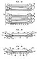
- FIG. 3Bshows an upper layer of the stacked microelectronic assembly of FIG. 3A .
- FIG. 3Cshows a base layer of the stacked microelectronic assembly of FIG. 3A .
- FIG. 4Ashows an enlarged fragmentary view of the stacked microelectronic assembly of FIG. 3A .
- FIG. 4Bshows another enlarged fragmentary view of FIG. 4A in accordance with certain preferred embodiments of the present invention.
- FIG. 4Cshows still another enlarged fragmentary view of FIG. 4A .
- FIG. 5Ashows a stacked microelectronic assembly with stiffening layers, in accordance with yet other preferred embodiments of the present invention.
- FIG. 5Bshows a stacked microelectronic assembly with stiffening layers, in accordance with further preferred embodiments of the present invention.
- FIGS. 6A and 6Bshow perspective views of a stacked microelectronic assembly with stiffening layers during various phases of the assembly process, in accordance with certain preferred embodiments of the present invention.
- FIG. 7Ashows a stacked microelectronic assembly with one or more stiffening layers, in accordance with still other preferred embodiments of the present invention.
- FIG. 7Bshows an upper subassembly layer of the stacked microelectronic assembly of FIG. 7A .
- FIG. 7Cshows a base layer of the stacked microelectronic assembly of FIG. 7A .
- FIG. 8shows a stacked microelectronic assembly with one or more stiffening layers, in accordance with other preferred embodiments of the present invention.
- FIG. 9shows a stacked microelectronic assembly with one or more stiffening layers, in accordance with still other preferred embodiments of the present invention.
- FIG. 10shows a stacked microelectronic assembly with stiffening layers, in accordance with still further preferred embodiments of the present invention.
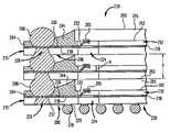
- FIG. 3Aillustrates a preferred embodiment of the stacked assembly of the present invention.
- Stacked assembly 200includes a plurality of N ⁇ 1 subassemblies 210 stacked one atop another with a base subassembly 220 occupying the bottom-most position in the stack.
- each subassembly 210 , 220includes a microelectronic element 201 , such as a semiconductor chip, having a front face 202 , a back face 203 opposite front face 202 and a plurality of contacts 205 exposed at front face 202 .
- contacts 205are exposed in a peripheral region of the chip face.
- Interposer 215is desirably a dielectric element having a first surface 216 , a second surface 217 opposite first surface 216 and a plurality of conductive pads (not shown) disposed on first surface 216 .
- Interposer 215also preferably has conductive elements 218 such as metallic traces thereon, with contacts 205 of chip 201 being electrically connected to conductive elements 218 .
- interposer 215is made of a flexible dielectric material such as polyimide tape.
- Interposer 215may also include one or more additional layers such as a conductive metal layer to serve as a power or ground plane, multiple layers of traces and multiple dielectric layers.
- the electrical connection between the contacts on face surface 202 and the pads on first surface 216may be made by any of the known methods of making electrical connections including, but not limited to, flip-chip bonding, wire bonding, tab bonding and the bonding methods disclosed in commonly assigned U.S. Pat. Nos. 5,148,265; 5,148,266; 5,518,964 and 5,536,909, the disclosures of which are incorporated herein by reference.
- at least one padis movable with respect to at least one contact.
- the preferred embodiments of the present inventionare not limited to the illustrated flip-chip configuration where face surface 202 faces first surface 216 of interposer 215 .
- the present inventionalso contemplates “face-up” configurations, wherein a face surface 202 of a chip faces away from interposer 215 .
- the utilization of lead-bonding methodologies disclosed in the U.S. Patents cited aboveare preferred because the resulting lead structures allow the formation of subassemblies having a very low overall height.
- fan-out connectors 208such as high-melting solder balls, are disposed on first surface 216 of interposer 215 and are electrically connected to at least some of conductive elements 218 on first surface 216 .
- Fan-out connectors 208are located so that, when subassemblies 210 , 220 are stacked one atop another, fan-out connectors 208 electrically interconnect the subassemblies within the stack, acting as vertical conductors.
- Fan-out connectors 208are preferably located around outer edges of chip 201 and adjacent peripheral regions of interposer 215 .
- Subassemblies 210 , 220also include respective stiffening layers 204 .
- Each stiffening layer 204is preferably made of an encapsulating material, such as a flexibilized epoxy or silicone elastomer, which surrounds both microelectronic element 201 and fan-out connectors 208 .
- the encapsulantalso desirably encapsulates the leads or other bonding structures 222 connecting contacts 205 of chip 201 to the conductive elements of interposer 215 .
- subassembly 220also preferably includes joining units 228 that are disposed on second surface 217 of interposer 215 and electrically connected to at least some of the pads on first surface 216 .
- Joining units 228may be used to attach assembly 200 to electrical contacts or pads on an external electronic element, such as those on a printed circuit board, or a second microelectronic assembly.
- a joining unitmay be formed by attaching a eutectic solder ball 228 to a conductive pad 229 affixed to second surface 217 of interposer 215 .
- peripheral region 206 of interposer 215is penetrated by vias 226 .
- Vias 226may be open at both ends or closed at one end to accommodate various methods of making electrical connections, as are known in the art.
- Vias 226may be electrically conductive.
- interposer 235is formed with openings 239 therein, and solder mass 239 is allowed to flow into an opening 238 to establish electrical contact with first surface 236 .
- the embodiment of FIG. 4Ballows interposer 235 to be constructed with a single metallic tape at a substantially lower cost than the embodiment of FIG. 4A , for which a bimetallic tape would more typically be employed.
- each subassemblypreferably includes fan-out connectors 208 , such as high-temperature solder balls, bonded to conductive elements 218 .
- the diameter of each connector 208is greater than the combined thicknesses of compliant layer 212 and microelectronic element 201 so that fan-out connector 208 extends beyond chip 201 to contact via 226 of the subassembly above it.
- back surface 203 of chip 201is in close proximity to second surface 217 of its adjacent subassembly.
- a layer 212 of compliant materialsuch as a gel or an elastomer is disposed between front face 202 of each chip 201 and surface 216 of interposer 215 .
- interposer 215 of each subassembly 210 , 220is mechanically decoupled from chip 201 and free to deform and deflect independent of the chip.
- Fan-out connectors 208may be provided as conventional “solid-core solder balls”, initially having coatings of solder which reflow to bond the connectors 208 to vias 226 and, preferably, to contact conductive elements 218 .
- stiffening layer 204is provided over top surface 216 , preferably surrounding microelectronic element 201 and fan-out connector 208 .
- stiffening layer 204is formed of an encapsulant, more preferably, of a flexibilized epoxy or silicone elastomer.
- the encapsulant of interposer 215fills gaps between the front face 202 of chip 201 and top surface 216 of interposer 215 , and encapsulates leads 222 .
- microelectronic element 201is mounted to surface 206 of interposer 215 in a “face-down” arrangement, that is, where the face surface 202 of element 201 confronts surface 206 .
- Leads 222electrically connect conductive elements 218 to contacts 205 .
- leads 222are flexible leads, preferably formed of copper, gold, alloys thereof and combinations thereof.
- leads 222may be formed according to the methods disclosed in commonly assigned U.S. Pat. Nos. 5,148,265; 5,148,266; 5,787,581 and 5,977,618. Referring to FIG. 4C , lead 222 a initially extends over slot 224 .
- Lead 222 amay have a notch or other weakened portion that provides a fracture point 223 in the lead.
- a toolmay be inserted into slot 224 to break lead 222 a and push it to the position of lead 222 , making contact with a contact 205 on chip face 202 .
- FIG. 4Acan readily be modified for “face-up” configurations, that is, the contact-bearing face of the chip faces away from interposer 215 , and that contacts 205 can be electrically connected to terminals on a surface of interposer 215 by wire bonding, flip-chip bonding, tab bonding, or other means of electrical bonding presently known in the art.
- an interposermay be fabricated without a conductive element 218 and that lead 222 may be fabricated so as to electrically connect a terminal on a surface of the interposer to a contact on chip face 202 .
- each subassembly 210 , 220preferably includes a spacer layer 212 disposed between front face 202 of microelectronic element 201 and interposer 215 .
- Spacer layer 212is preferably compliant. Preferred materials for the spacer layers 212 include epoxies and silicones, with flexibilized epoxies and silicone elastomers being particularly preferred. Spacer layer 212 may comprise a single pad of material, as depicted in FIG. 4A , or a plurality of such pads.
- the spacer layer 212absorbs the stress of differential thermal expansion of interposer 215 and the microelectronic element 201 and inhibits deformation of the flexible dielectric structure during handling and installation of the subassembly.
- Spacer layer 212is preferably positioned to avoid obstructing movement of flexible leads 222 or interfering with contact between lead 222 and electrical contact 205 .
- only the base subassembly 220 of the stacked microelectronic assemblyis provided with a compliant spacer layer 212 , as the effects of differential thermal expansion typically are most critical at the bottom-most subassembly in the stack.
- the individual subassemblies 210 , 220are fabricated as described above. Each subassembly 210 , 220 may be tested separately by engaging vias 226 with contacts of a test socket, or by engaging fan-out connector 208 in a socket. The chip 201 , leads 222 and connections can then be tested by actual operation of the chip. After testing, the individual subassemblies 210 , 220 are stacked one atop another so that chips 201 generally overlie one another in front face to rear face disposition, and so that peripheral regions 206 of the various interposers 215 are aligned with one another.
- vias 226 of the various interposers 215 and the fan-out connectors 208 associated therewithare also aligned one with another.
- the connector 208 associated with its respective via 226 on one interposermakes contact with a corresponding via 226 on the next interposer in the stack.
- joining units 228such as solder balls, are disposed on second surface 217 of the bottom-most interposer 215 and are electrically connected to at least some conductive elements 218 on first surface 216 .
- Joining units 228may be used to attach the stacked microelectronic assembly to electrical circuit contacts or pads on a printed circuit board or a second microelectronic assembly.
- microelectronic elements 601are attached to a strip of interposer 615 and electrically connected to the interposer as described herein, and fan-out connectors 608 are affixed to surface 616 of interposer 615 as described herein.
- an encapsulantsuch as a flexibilized epoxy or silicone elastomer, is provided over top surface 616 of interposer 615 to surround microelectronic element 601 and fan-out connectors 608 .
- fan-out connectors 708are affixed to second surface 717 of interposer 715 .
- Stiffening layer 704is joined to second surface 717 so as to surround fan-out connectors 708 .
- Stiffening layer 704includes a depression or opening 705 formed therein so that when subassemblies 710 , 720 are stacked one atop another, the respective encapsulated chip 711 , 721 of the lower subassembly 711 , 721 fits within the opening 705 of the upper assembly.
- the bottom subassembly 720 in the stack 700is fabricated without fan-out connectors.
- Subassembly 720may be provided with joining units 728 of the types discussed herein for other embodiments of the present invention.
- FIGS. 3A , 4 A and 7 Adepict embodiments wherein the centers of the microelectronic elements are aligned with each other
- the present inventionalso includes embodiments wherein at least one microelectronic element overlies other microelectronic elements in such a way that the centers of such elements are not aligned.
- the microelectronic elements of the present inventionare not limited to single semiconductor chips. Alternatively, a plurality of semiconductor chips may be laid side by side along the first surface of the interposer or stacked one atop another within a subassembly without departing from the invention herein disclosed.
- vias 226may serve as fan-out connectors in embodiments where electrically conductive vias 226 are aligned one with another, with an electrically conductive rod inserted through the aligned vias 226 to provide the electrical interconnection between the subassemblies.
- other methods of establishing vertical electrical connectionssuch as those disclosed in commonly assigned U.S. Pat. No. 5,861,666, may be used without departing from the scope of the invention.
- stiffening layer 204would be modified as needed to allow electrical connections to be formed according to the connection method used.
- the stiffening layer 204may be may be formed from materials other than the encapsulants discussed herein.
- suitable materialsinclude, but are not limited to, glass sheet, glass-filled epoxy, ceramic materials, or a plastic sheet, so long as the stiffening layer surrounds the microelectronic elements in the central region of the interposer and the fan-out connectors in the peripheral regions of the interposer.
- the stiffening layermay be formed from epoxy or elastomer materials that have a modulus different from the modulus of the materials used to encapsulate leads 222 or to form compliant layer 212 .
- the present inventionis not limited by any particular theory of operation, it is believed that providing a stiffening layer on the interposer surface creates a subassembly that is more rigid than those fabricated by methods currently in use, but which still provides some flexibility in the subassembly design.
- a stiffening layer that surrounds the microelectronic element and/or fan-out connectorsfurther increases the rigidity of the resulting structure.
- the methods of the present inventionmay be used to fabricate subassemblies with single or multiple rows of overhung fan-out connectors such as the embodiment of FIG. 5A , or with dies of differing sizes, such as the embodiment of FIG. 5B .
- each subassembly 210 , 220preferably has a height or thickness that is about 1 millimeter or less. In more preferred embodiments, the subassembly has a thickness of about 700 microns or less.
- the preferred lead structures, such as leads 222have a height of 500 microns or less. Such vertically extensive leads allow the contacts on the chip face to move relative to the pads on the first surface of the dielectric element in response to differences in thermal expansion among the elements of the assembly.
- the stiffening layer 204provides the desired stiffness without adding additional height to the subassembly.
- the stacked assembly of the present inventioncan be fabricated using readily available techniques.
- the assemblypreferably provides electrically conductive pathways connecting the chips in the stack to one another and to external circuit elements with low impedance and short circuit path lengths, while minimizing mechanical stresses caused by differences in thermal expansion between the chip and the dielectric elements.
- the presence of stiffening layers in one or more of the subassembliesresult in a more rigid structure than stacked assemblies formed by techniques presently in use.
- a stacked microelectronic assembly 800includes a first subassembly 810 stacked atop and electrically interconnected with a second subassembly 820 .
- the first subassemblyincludes a flexible substrate 815 having a first surface 816 and a bottom surface 818 remote therefrom.
- First subassembly 810also includes conductive elements 818 , such as conductive traces provided over the top surface 816 of flexible substrate 815 .
- First subassembly 810also includes a microelectronic element 801 , such as a semiconductor chip, including a front contact bearing face 802 and back face 803 remote therefrom.
- microelectronic element 801is mounted above the top surface 816 of flexible substrate 815 with back face 803 facing top surface 816 .
- the microelectronic element 801is electrically interconnected with conductive element 818 by wire bonds 822 .
- wire bonds 822have first ends 823 attached to contacts (not shown) on front face 802 of microelectronic element 801 and second ends 824 attached to conductive element 818 .
- Pan-out connectors 808such as high-melting temperature solder balls, are disposed on top surface 816 of flexible substrate 815 and are electrically connected with at least some of the conductive elements 818 extending over top surface 816 .
- the fan-out connectors 808are preferably located atop the surface 816 of flexible substrate 815 so that when the subassemblies 810 , 820 are stacked one atop another, the fan-out connectors 808 electrically interconnect the subassemblies within the stack, thereby acting as vertical conductors.
- the fan-out connectors 808extend beyond the outer edges of the microelectronic element 801 .
- the fan-out connectors 808are located adjacent peripheral regions 825 of the flexible substrate 815 .
- Subassembly 810also preferably includes a stiffening layer 804 made of an encapsulating material.
- the stiffening layer 804is made of an encapsulating material such as flexibilized epoxy or silicone elastomers, which surround both microelectronic element 801 and fan-out connectors 808 .
- the stiffening layer 804may also encapsulate the wire bonds 822 .
- the stiffening layercompletely encapsulates the wire bonds 822 and the microelectronic element 801 . In other embodiments, however, such as the one shown in FIG. 8 , the stiffening layer encapsulates only certain sections of the wire bond 822 .
- Stacked microelectronic assembly 800also includes second subassembly 820 having flexible substrate 815 ′, microelectronic element 801 ′, fan-out connectors 808 ′, wire bonds 822 ′ and stiffening layer 804 ′.
- second subassembly 820is substantially similar to first subassembly 810 .
- the stiffening layer 804 ′ of second subassembly 820adds rigidity to the subassembly in the vicinity of the peripheral region 825 ′ of flexible substrate 815 ′.
- Stacked microelectronic assembly 800also includes one or more joining units 828 ′ provided over second surface 818 ′ of flexible substrate 815 ′.
- the joining units 828 ′are preferably electrically interconnected to at least some of the fan-out connectors 208 and/or microelectronic elements 801 , 801 ′.
- Joining units 828 ′are preferably used to attach the stacked microelectronic assembly to an external element, such as a substrate having electrical contacts or pads.
- FIG. 9shows a stacked microelectronic assembly 900 , in accordance with another preferred embodiment of the present invention, including first subassembly 910 stacked over second subassembly 920 .
- First subassembly 910includes substrate 915 having top surface 716 and microelectronic element 901 having back face 903 facing top surface 716 .
- the front fact 902faces away from top surface 916 and has contacts (not shown) that are electrically interconnected with conductive elements 919 by wire bonds 922 .
- First subassembly 910includes fan-out connectors 909 at peripheral regions 925 of flexible substrate 915 .
- First subassembly 910also includes a stiffening layer 904 that extends around microelectronic element 901 and fan-out connectors 909 .
- Second subassembly 920includes microelectronic element 901 ′ having a contact bearing front face 902 ′ that faces top surface 916 ′ of flexible substrate 915 ′.
- the mounting of the microelectronic element 901 ′ over flexible substrate 915 ′is commonly referred to as a “flip-chip” assembly.
- the microelectronic element 901 ′is electrically interconnected with conductive elements 919 ′ extending over first surface 916 ′ using flexible leads 922 ′.
- FIG. 10shows a stacked microelectronic assembly 1000 including a first subassembly 1010 stacked over a second subassembly 1020 .
- First subassembly 1010includes a microelectronic element 1001 having a contact bearing face 1002 facing away from top surface 1016 of flexible substrate 1015 .
- Microelectronic element 1001is electrically interconnected with conductive elements 1018 by wire bonds 1022 .
- First subassembly 1010includes fan-out connectors 1008 provided in peripheral regions 1025 of flexible substrate 1015 .
- a stiffening layer 1004surrounds microelectronic element 1001 and fan-out connectors 1008 for providing stiffening at peripheral regions 1025 of flexible substrate 1015 , thereby facilitating testing and handling of the subassembly.
- the first subassembly 1010includes a compliant layer disposed between the microelectronic element 1001 and the substrate 1015 to permit relative movement of the microelectronic element and the substrate during thermal cycling of the subassembly.
- the compliant layerincludes a plurality of compliant pads 1030 spaced from one another for defining channels or gaps therebetween.
- the encapsulant layer or stiffening layer 1004is disposed in the channels between the compliant pads 1030 .
- Second subassembly 1020includes generally similar elements as those described above in first subassembly 1010 , however, second subassembly 1020 includes a microelectronic element 1001 ′ that is substantially larger than microelectronic element 1001 of first subassembly 1010 .
- the present inventionhas applicability in the microelectronics industry.
Landscapes
- Engineering & Computer Science (AREA)
- Microelectronics & Electronic Packaging (AREA)
- Power Engineering (AREA)
- Computer Hardware Design (AREA)
- Physics & Mathematics (AREA)
- Condensed Matter Physics & Semiconductors (AREA)
- General Physics & Mathematics (AREA)
- Manufacturing & Machinery (AREA)
- Connecting Device With Holders (AREA)
Abstract
Description
Claims (36)
Priority Applications (1)
| Application Number | Priority Date | Filing Date | Title |
|---|---|---|---|
| US10/487,482US7605479B2 (en) | 2001-08-22 | 2002-08-22 | Stacked chip assembly with encapsulant layer |
Applications Claiming Priority (3)
| Application Number | Priority Date | Filing Date | Title |
|---|---|---|---|
| US31404201P | 2001-08-22 | 2001-08-22 | |
| PCT/US2002/026805WO2003019654A1 (en) | 2001-08-22 | 2002-08-22 | Stacked chip assembly with stiffening layer |
| US10/487,482US7605479B2 (en) | 2001-08-22 | 2002-08-22 | Stacked chip assembly with encapsulant layer |
Publications (2)
| Publication Number | Publication Date |
|---|---|
| US20050035440A1 US20050035440A1 (en) | 2005-02-17 |
| US7605479B2true US7605479B2 (en) | 2009-10-20 |
Family
ID=23218301
Family Applications (1)
| Application Number | Title | Priority Date | Filing Date |
|---|---|---|---|
| US10/487,482Expired - LifetimeUS7605479B2 (en) | 2001-08-22 | 2002-08-22 | Stacked chip assembly with encapsulant layer |
Country Status (2)
| Country | Link |
|---|---|
| US (1) | US7605479B2 (en) |
| WO (1) | WO2003019654A1 (en) |
Cited By (22)
| Publication number | Priority date | Publication date | Assignee | Title |
|---|---|---|---|---|
| US8466545B1 (en)* | 2004-06-08 | 2013-06-18 | Amkor Technology, Inc. | Stackable semiconductor package |
| US9548273B2 (en) | 2014-12-04 | 2017-01-17 | Invensas Corporation | Integrated circuit assemblies with rigid layers used for protection against mechanical thinning and for other purposes, and methods of fabricating such assemblies |
| US9735084B2 (en) | 2014-12-11 | 2017-08-15 | Invensas Corporation | Bond via array for thermal conductivity |
| US9761554B2 (en) | 2015-05-07 | 2017-09-12 | Invensas Corporation | Ball bonding metal wire bond wires to metal pads |
| US9812402B2 (en) | 2015-10-12 | 2017-11-07 | Invensas Corporation | Wire bond wires for interference shielding |
| US9842745B2 (en) | 2012-02-17 | 2017-12-12 | Invensas Corporation | Heat spreading substrate with embedded interconnects |
| US9888579B2 (en) | 2015-03-05 | 2018-02-06 | Invensas Corporation | Pressing of wire bond wire tips to provide bent-over tips |
| US9911718B2 (en) | 2015-11-17 | 2018-03-06 | Invensas Corporation | ‘RDL-First’ packaged microelectronic device for a package-on-package device |
| US9935075B2 (en) | 2016-07-29 | 2018-04-03 | Invensas Corporation | Wire bonding method and apparatus for electromagnetic interference shielding |
| US9947641B2 (en) | 2014-05-30 | 2018-04-17 | Invensas Corporation | Wire bond support structure and microelectronic package including wire bonds therefrom |
| US9984992B2 (en) | 2015-12-30 | 2018-05-29 | Invensas Corporation | Embedded wire bond wires for vertical integration with separate surface mount and wire bond mounting surfaces |
| US10008469B2 (en) | 2015-04-30 | 2018-06-26 | Invensas Corporation | Wafer-level packaging using wire bond wires in place of a redistribution layer |
| US10062661B2 (en) | 2011-05-03 | 2018-08-28 | Tessera, Inc. | Package-on-package assembly with wire bonds to encapsulation surface |
| US10170412B2 (en) | 2012-05-22 | 2019-01-01 | Invensas Corporation | Substrate-less stackable package with wire-bond interconnect |
| US10181457B2 (en) | 2015-10-26 | 2019-01-15 | Invensas Corporation | Microelectronic package for wafer-level chip scale packaging with fan-out |
| US10290613B2 (en) | 2013-11-22 | 2019-05-14 | Invensas Corporation | Multiple bond via arrays of different wire heights on a same substrate |
| US10299368B2 (en) | 2016-12-21 | 2019-05-21 | Invensas Corporation | Surface integrated waveguides and circuit structures therefor |
| US10381326B2 (en) | 2014-05-28 | 2019-08-13 | Invensas Corporation | Structure and method for integrated circuits packaging with increased density |
| US10490528B2 (en) | 2015-10-12 | 2019-11-26 | Invensas Corporation | Embedded wire bond wires |
| US11189595B2 (en) | 2011-10-17 | 2021-11-30 | Invensas Corporation | Package-on-package assembly with wire bond vias |
| US11236012B2 (en) | 2018-03-28 | 2022-02-01 | Corning Incorporated | Boron phosphate glass-ceramics with low dielectric loss |
| US11404338B2 (en) | 2014-01-17 | 2022-08-02 | Invensas Corporation | Fine pitch bva using reconstituted wafer with area array accessible for testing |
Families Citing this family (92)
| Publication number | Priority date | Publication date | Assignee | Title |
|---|---|---|---|---|
| US5484959A (en)* | 1992-12-11 | 1996-01-16 | Staktek Corporation | High density lead-on-package fabrication method and apparatus |
| US6323060B1 (en) | 1999-05-05 | 2001-11-27 | Dense-Pac Microsystems, Inc. | Stackable flex circuit IC package and method of making same |
| US6262895B1 (en) | 2000-01-13 | 2001-07-17 | John A. Forthun | Stackable chip package with flex carrier |
| US7335995B2 (en) | 2001-10-09 | 2008-02-26 | Tessera, Inc. | Microelectronic assembly having array including passive elements and interconnects |
| WO2003032370A2 (en) | 2001-10-09 | 2003-04-17 | Tessera, Inc. | Stacked packages |
| US6940729B2 (en) | 2001-10-26 | 2005-09-06 | Staktek Group L.P. | Integrated circuit stacking system and method |
| US6914324B2 (en)* | 2001-10-26 | 2005-07-05 | Staktek Group L.P. | Memory expansion and chip scale stacking system and method |
| US7310458B2 (en) | 2001-10-26 | 2007-12-18 | Staktek Group L.P. | Stacked module systems and methods |
| US7053478B2 (en)* | 2001-10-26 | 2006-05-30 | Staktek Group L.P. | Pitch change and chip scale stacking system |
| US7485951B2 (en)* | 2001-10-26 | 2009-02-03 | Entorian Technologies, Lp | Modularized die stacking system and method |
| US20050056921A1 (en)* | 2003-09-15 | 2005-03-17 | Staktek Group L.P. | Stacked module systems and methods |
| US6956284B2 (en) | 2001-10-26 | 2005-10-18 | Staktek Group L.P. | Integrated circuit stacking system and method |
| US20030234443A1 (en) | 2001-10-26 | 2003-12-25 | Staktek Group, L.P. | Low profile stacking system and method |
| US6576992B1 (en)* | 2001-10-26 | 2003-06-10 | Staktek Group L.P. | Chip scale stacking system and method |
| US7656678B2 (en) | 2001-10-26 | 2010-02-02 | Entorian Technologies, Lp | Stacked module systems |
| US20040195666A1 (en)* | 2001-10-26 | 2004-10-07 | Julian Partridge | Stacked module systems and methods |
| US7371609B2 (en)* | 2001-10-26 | 2008-05-13 | Staktek Group L.P. | Stacked module systems and methods |
| US7202555B2 (en)* | 2001-10-26 | 2007-04-10 | Staktek Group L.P. | Pitch change and chip scale stacking system and method |
| US20050009234A1 (en)* | 2001-10-26 | 2005-01-13 | Staktek Group, L.P. | Stacked module systems and methods for CSP packages |
| US20060255446A1 (en)* | 2001-10-26 | 2006-11-16 | Staktek Group, L.P. | Stacked modules and method |
| US7026708B2 (en)* | 2001-10-26 | 2006-04-11 | Staktek Group L.P. | Low profile chip scale stacking system and method |
| US7081373B2 (en)* | 2001-12-14 | 2006-07-25 | Staktek Group, L.P. | CSP chip stack with flex circuit |
| WO2004017399A1 (en) | 2002-08-16 | 2004-02-26 | Tessera, Inc. | Microelectronic packages with self-aligning features |
| US7294928B2 (en) | 2002-09-06 | 2007-11-13 | Tessera, Inc. | Components, methods and assemblies for stacked packages |
| US7071547B2 (en) | 2002-09-11 | 2006-07-04 | Tessera, Inc. | Assemblies having stacked semiconductor chips and methods of making same |
| WO2004034434A2 (en) | 2002-10-11 | 2004-04-22 | Tessera, Inc. | Components, methods and assemblies for multi-chip packages |
| US20040245615A1 (en)* | 2003-06-03 | 2004-12-09 | Staktek Group, L.P. | Point to point memory expansion system and method |
| US6991961B2 (en) | 2003-06-18 | 2006-01-31 | Medtronic, Inc. | Method of forming a high-voltage/high-power die package |
| US7542304B2 (en)* | 2003-09-15 | 2009-06-02 | Entorian Technologies, Lp | Memory expansion and integrated circuit stacking system and method |
| US20060033187A1 (en)* | 2004-08-12 | 2006-02-16 | Staktek Group, L.P. | Rugged CSP module system and method |
| US20060043558A1 (en)* | 2004-09-01 | 2006-03-02 | Staktek Group L.P. | Stacked integrated circuit cascade signaling system and method |
| US20060051912A1 (en)* | 2004-09-09 | 2006-03-09 | Ati Technologies Inc. | Method and apparatus for a stacked die configuration |
| US20060055024A1 (en)* | 2004-09-14 | 2006-03-16 | Staktek Group, L.P. | Adapted leaded integrated circuit module |
| US20060072297A1 (en)* | 2004-10-01 | 2006-04-06 | Staktek Group L.P. | Circuit Module Access System and Method |
| KR101313391B1 (en) | 2004-11-03 | 2013-10-01 | 테세라, 인코포레이티드 | Stacked packaging improvements |
| US20060118936A1 (en)* | 2004-12-03 | 2006-06-08 | Staktek Group L.P. | Circuit module component mounting system and method |
| US7183638B2 (en)* | 2004-12-30 | 2007-02-27 | Intel Corporation | Embedded heat spreader |
| US7309914B2 (en)* | 2005-01-20 | 2007-12-18 | Staktek Group L.P. | Inverted CSP stacking system and method |
| US20060175693A1 (en)* | 2005-02-04 | 2006-08-10 | Staktek Group, L.P. | Systems, methods, and apparatus for generating ball-out matrix configuration output for a flex circuit |
| US20080203552A1 (en)* | 2005-02-15 | 2008-08-28 | Unisemicon Co., Ltd. | Stacked Package and Method of Fabricating the Same |
| US7745912B2 (en)* | 2005-03-25 | 2010-06-29 | Intel Corporation | Stress absorption layer and cylinder solder joint method and apparatus |
| US20060244114A1 (en)* | 2005-04-28 | 2006-11-02 | Staktek Group L.P. | Systems, methods, and apparatus for connecting a set of contacts on an integrated circuit to a flex circuit via a contact beam |
| US20060286717A1 (en)* | 2005-05-06 | 2006-12-21 | Tessera, Inc. | Stacked microelectronic assemblies having basal compliant layers |
| US7033861B1 (en) | 2005-05-18 | 2006-04-25 | Staktek Group L.P. | Stacked module systems and method |
| US20070080441A1 (en)* | 2005-08-18 | 2007-04-12 | Scott Kirkman | Thermal expansion compensation graded IC package |
| US7576995B2 (en)* | 2005-11-04 | 2009-08-18 | Entorian Technologies, Lp | Flex circuit apparatus and method for adding capacitance while conserving circuit board surface area |
| US8058101B2 (en) | 2005-12-23 | 2011-11-15 | Tessera, Inc. | Microelectronic packages and methods therefor |
| US7605454B2 (en) | 2006-01-11 | 2009-10-20 | Entorian Technologies, Lp | Memory card and method for devising |
| US7608920B2 (en)* | 2006-01-11 | 2009-10-27 | Entorian Technologies, Lp | Memory card and method for devising |
| US7508069B2 (en) | 2006-01-11 | 2009-03-24 | Entorian Technologies, Lp | Managed memory component |
| US7304382B2 (en) | 2006-01-11 | 2007-12-04 | Staktek Group L.P. | Managed memory component |
| US7508058B2 (en) | 2006-01-11 | 2009-03-24 | Entorian Technologies, Lp | Stacked integrated circuit module |
| US20070158821A1 (en)* | 2006-01-11 | 2007-07-12 | Leland Szewerenko | Managed memory component |
| US20070164416A1 (en)* | 2006-01-17 | 2007-07-19 | James Douglas Wehrly | Managed memory component |
| US20070262429A1 (en)* | 2006-05-15 | 2007-11-15 | Staktek Group, L.P. | Perimeter stacking system and method |
| US7545029B2 (en) | 2006-08-18 | 2009-06-09 | Tessera, Inc. | Stack microelectronic assemblies |
| US20080099910A1 (en)* | 2006-08-31 | 2008-05-01 | Ati Technologies Inc. | Flip-Chip Semiconductor Package with Encapsulant Retaining Structure and Strip |
| US7468553B2 (en)* | 2006-10-20 | 2008-12-23 | Entorian Technologies, Lp | Stackable micropackages and stacked modules |
| US7417310B2 (en) | 2006-11-02 | 2008-08-26 | Entorian Technologies, Lp | Circuit module having force resistant construction |
| US7763983B2 (en) | 2007-07-02 | 2010-07-27 | Tessera, Inc. | Stackable microelectronic device carriers, stacked device carriers and methods of making the same |
| US8217514B2 (en)* | 2008-04-07 | 2012-07-10 | Stats Chippac Ltd. | Integrated circuit packaging system with warpage control system and method of manufacture thereof |
| US8498125B2 (en)* | 2008-06-09 | 2013-07-30 | Schlumberger Technology Corporation | Instrumentation package in a downhole tool string component |
| US8183677B2 (en)* | 2008-11-26 | 2012-05-22 | Infineon Technologies Ag | Device including a semiconductor chip |
| US8482111B2 (en) | 2010-07-19 | 2013-07-09 | Tessera, Inc. | Stackable molded microelectronic packages |
| US9159708B2 (en) | 2010-07-19 | 2015-10-13 | Tessera, Inc. | Stackable molded microelectronic packages with area array unit connectors |
| KR101075241B1 (en) | 2010-11-15 | 2011-11-01 | 테세라, 인코포레이티드 | Microelectronic package with terminals in dielectric member |
| US20120146206A1 (en) | 2010-12-13 | 2012-06-14 | Tessera Research Llc | Pin attachment |
| US8618659B2 (en) | 2011-05-03 | 2013-12-31 | Tessera, Inc. | Package-on-package assembly with wire bonds to encapsulation surface |
| US8872318B2 (en) | 2011-08-24 | 2014-10-28 | Tessera, Inc. | Through interposer wire bond using low CTE interposer with coarse slot apertures |
| US9349706B2 (en) | 2012-02-24 | 2016-05-24 | Invensas Corporation | Method for package-on-package assembly with wire bonds to encapsulation surface |
| US8372741B1 (en) | 2012-02-24 | 2013-02-12 | Invensas Corporation | Method for package-on-package assembly with wire bonds to encapsulation surface |
| US9385006B2 (en)* | 2012-06-21 | 2016-07-05 | STATS ChipPAC Pte. Ltd. | Semiconductor device and method of forming an embedded SOP fan-out package |
| US9391008B2 (en) | 2012-07-31 | 2016-07-12 | Invensas Corporation | Reconstituted wafer-level package DRAM |
| US9502390B2 (en) | 2012-08-03 | 2016-11-22 | Invensas Corporation | BVA interposer |
| US8975738B2 (en) | 2012-11-12 | 2015-03-10 | Invensas Corporation | Structure for microelectronic packaging with terminals on dielectric mass |
| US8878353B2 (en) | 2012-12-20 | 2014-11-04 | Invensas Corporation | Structure for microelectronic packaging with bond elements to encapsulation surface |
| US9136254B2 (en) | 2013-02-01 | 2015-09-15 | Invensas Corporation | Microelectronic package having wire bond vias and stiffening layer |
| US9023691B2 (en) | 2013-07-15 | 2015-05-05 | Invensas Corporation | Microelectronic assemblies with stack terminals coupled by connectors extending through encapsulation |
| US8883563B1 (en) | 2013-07-15 | 2014-11-11 | Invensas Corporation | Fabrication of microelectronic assemblies having stack terminals coupled by connectors extending through encapsulation |
| US9034696B2 (en) | 2013-07-15 | 2015-05-19 | Invensas Corporation | Microelectronic assemblies having reinforcing collars on connectors extending through encapsulation |
| US9167710B2 (en) | 2013-08-07 | 2015-10-20 | Invensas Corporation | Embedded packaging with preformed vias |
| US9685365B2 (en) | 2013-08-08 | 2017-06-20 | Invensas Corporation | Method of forming a wire bond having a free end |
| US20150076714A1 (en) | 2013-09-16 | 2015-03-19 | Invensas Corporation | Microelectronic element with bond elements to encapsulation surface |
| US9082753B2 (en) | 2013-11-12 | 2015-07-14 | Invensas Corporation | Severing bond wire by kinking and twisting |
| US9087815B2 (en) | 2013-11-12 | 2015-07-21 | Invensas Corporation | Off substrate kinking of bond wire |
| US9379074B2 (en) | 2013-11-22 | 2016-06-28 | Invensas Corporation | Die stacks with one or more bond via arrays of wire bond wires and with one or more arrays of bump interconnects |
| US9263394B2 (en) | 2013-11-22 | 2016-02-16 | Invensas Corporation | Multiple bond via arrays of different wire heights on a same substrate |
| US9459288B2 (en)* | 2014-01-16 | 2016-10-04 | Infineon Technologies Ag | Wide interposer for an electronic testing system |
| US9214454B2 (en) | 2014-03-31 | 2015-12-15 | Invensas Corporation | Batch process fabrication of package-on-package microelectronic assemblies |
| US9646917B2 (en) | 2014-05-29 | 2017-05-09 | Invensas Corporation | Low CTE component with wire bond interconnects |
| US10332854B2 (en) | 2015-10-23 | 2019-06-25 | Invensas Corporation | Anchoring structure of fine pitch bva |
| US9659848B1 (en) | 2015-11-18 | 2017-05-23 | Invensas Corporation | Stiffened wires for offset BVA |
Citations (25)
| Publication number | Priority date | Publication date | Assignee | Title |
|---|---|---|---|---|
| US4604644A (en)* | 1985-01-28 | 1986-08-05 | International Business Machines Corporation | Solder interconnection structure for joining semiconductor devices to substrates that have improved fatigue life, and process for making |
| JPS62226307A (en) | 1986-03-28 | 1987-10-05 | Toshiba Corp | robot equipment |
| US5148266A (en) | 1990-09-24 | 1992-09-15 | Ist Associates, Inc. | Semiconductor chip assemblies having interposer and flexible lead |
| US5438224A (en)* | 1992-04-23 | 1995-08-01 | Motorola, Inc. | Integrated circuit package having a face-to-face IC chip arrangement |
| US5518964A (en) | 1994-07-07 | 1996-05-21 | Tessera, Inc. | Microelectronic mounting with multiple lead deformation and bonding |
| US5536909A (en) | 1992-07-24 | 1996-07-16 | Tessera, Inc. | Semiconductor connection components and methods with releasable lead support |
| US5659952A (en)* | 1994-09-20 | 1997-08-26 | Tessera, Inc. | Method of fabricating compliant interface for semiconductor chip |
| US5831836A (en)* | 1992-01-30 | 1998-11-03 | Lsi Logic | Power plane for semiconductor device |
| US5977618A (en) | 1992-07-24 | 1999-11-02 | Tessera, Inc. | Semiconductor connection components and methods with releasable lead support |
| US6121676A (en) | 1996-12-13 | 2000-09-19 | Tessera, Inc. | Stacked microelectronic assembly and method therefor |
| US6157080A (en)* | 1997-11-06 | 2000-12-05 | Sharp Kabushiki Kaisha | Semiconductor device using a chip scale package |
| US6225688B1 (en) | 1997-12-11 | 2001-05-01 | Tessera, Inc. | Stacked microelectronic assembly and method therefor |
| US20010028114A1 (en)* | 2000-03-27 | 2001-10-11 | Kabushiki Kaisha Toshiba | Semiconductor device including memory unit and semiconductor module including memory units |
| US6303997B1 (en)* | 1998-04-08 | 2001-10-16 | Anam Semiconductor, Inc. | Thin, stackable semiconductor packages |
| US6313528B1 (en)* | 1996-12-13 | 2001-11-06 | Tessera, Inc. | Compliant multichip package |
| US6316838B1 (en)* | 1999-10-29 | 2001-11-13 | Fujitsu Limited | Semiconductor device |
| US6388333B1 (en)* | 1999-11-30 | 2002-05-14 | Fujitsu Limited | Semiconductor device having protruding electrodes higher than a sealed portion |
| US6531784B1 (en)* | 2000-06-02 | 2003-03-11 | Amkor Technology, Inc. | Semiconductor package with spacer strips |
| US6630730B2 (en)* | 2000-04-28 | 2003-10-07 | Micron Technology, Inc. | Semiconductor device assemblies including interposers with dams protruding therefrom |
| US6746894B2 (en)* | 2001-03-30 | 2004-06-08 | Micron Technology, Inc. | Ball grid array interposer, packages and methods |
| US6762078B2 (en)* | 1999-05-20 | 2004-07-13 | Amkor Technology, Inc. | Semiconductor package having semiconductor chip within central aperture of substrate |
| US6774473B1 (en)* | 1999-07-30 | 2004-08-10 | Ming-Tung Shen | Semiconductor chip module |
| US6777787B2 (en)* | 2000-03-28 | 2004-08-17 | Rohm Co., Ltd. | Semiconductor device with warp preventing board joined thereto |
| US6844619B2 (en)* | 2000-12-01 | 2005-01-18 | Nec Corporation | Compact semiconductor device capable of mounting a plurality of semiconductor chips with high density and method of manufacturing the same |
| US6867499B1 (en)* | 1999-09-30 | 2005-03-15 | Skyworks Solutions, Inc. | Semiconductor packaging |
Family Cites Families (4)
| Publication number | Priority date | Publication date | Assignee | Title |
|---|---|---|---|---|
| JP2780649B2 (en)* | 1994-09-30 | 1998-07-30 | 日本電気株式会社 | Semiconductor device |
| US5689135A (en)* | 1995-12-19 | 1997-11-18 | Micron Technology, Inc. | Multi-chip device and method of fabrication employing leads over and under processes |
| US5748452A (en)* | 1996-07-23 | 1998-05-05 | International Business Machines Corporation | Multi-electronic device package |
| US6137164A (en)* | 1998-03-16 | 2000-10-24 | Texas Instruments Incorporated | Thin stacked integrated circuit device |
- 2002
- 2002-08-22USUS10/487,482patent/US7605479B2/ennot_activeExpired - Lifetime
- 2002-08-22WOPCT/US2002/026805patent/WO2003019654A1/ennot_activeApplication Discontinuation
Patent Citations (27)
| Publication number | Priority date | Publication date | Assignee | Title |
|---|---|---|---|---|
| US4604644A (en)* | 1985-01-28 | 1986-08-05 | International Business Machines Corporation | Solder interconnection structure for joining semiconductor devices to substrates that have improved fatigue life, and process for making |
| JPS62226307A (en) | 1986-03-28 | 1987-10-05 | Toshiba Corp | robot equipment |
| US5148266A (en) | 1990-09-24 | 1992-09-15 | Ist Associates, Inc. | Semiconductor chip assemblies having interposer and flexible lead |
| US5831836A (en)* | 1992-01-30 | 1998-11-03 | Lsi Logic | Power plane for semiconductor device |
| US5438224A (en)* | 1992-04-23 | 1995-08-01 | Motorola, Inc. | Integrated circuit package having a face-to-face IC chip arrangement |
| US5977618A (en) | 1992-07-24 | 1999-11-02 | Tessera, Inc. | Semiconductor connection components and methods with releasable lead support |
| US5787581A (en) | 1992-07-24 | 1998-08-04 | Tessera, Inc. | Methods of making semiconductor connection components with releasable load support |
| US5536909A (en) | 1992-07-24 | 1996-07-16 | Tessera, Inc. | Semiconductor connection components and methods with releasable lead support |
| US5518964A (en) | 1994-07-07 | 1996-05-21 | Tessera, Inc. | Microelectronic mounting with multiple lead deformation and bonding |
| US5659952A (en)* | 1994-09-20 | 1997-08-26 | Tessera, Inc. | Method of fabricating compliant interface for semiconductor chip |
| US6313528B1 (en)* | 1996-12-13 | 2001-11-06 | Tessera, Inc. | Compliant multichip package |
| US6121676A (en) | 1996-12-13 | 2000-09-19 | Tessera, Inc. | Stacked microelectronic assembly and method therefor |
| US6699730B2 (en) | 1996-12-13 | 2004-03-02 | Tessers, Inc. | Stacked microelectronic assembly and method therefor |
| US6157080A (en)* | 1997-11-06 | 2000-12-05 | Sharp Kabushiki Kaisha | Semiconductor device using a chip scale package |
| US6225688B1 (en) | 1997-12-11 | 2001-05-01 | Tessera, Inc. | Stacked microelectronic assembly and method therefor |
| US6303997B1 (en)* | 1998-04-08 | 2001-10-16 | Anam Semiconductor, Inc. | Thin, stackable semiconductor packages |
| US6762078B2 (en)* | 1999-05-20 | 2004-07-13 | Amkor Technology, Inc. | Semiconductor package having semiconductor chip within central aperture of substrate |
| US6774473B1 (en)* | 1999-07-30 | 2004-08-10 | Ming-Tung Shen | Semiconductor chip module |
| US6867499B1 (en)* | 1999-09-30 | 2005-03-15 | Skyworks Solutions, Inc. | Semiconductor packaging |
| US6316838B1 (en)* | 1999-10-29 | 2001-11-13 | Fujitsu Limited | Semiconductor device |
| US6388333B1 (en)* | 1999-11-30 | 2002-05-14 | Fujitsu Limited | Semiconductor device having protruding electrodes higher than a sealed portion |
| US20010028114A1 (en)* | 2000-03-27 | 2001-10-11 | Kabushiki Kaisha Toshiba | Semiconductor device including memory unit and semiconductor module including memory units |
| US6777787B2 (en)* | 2000-03-28 | 2004-08-17 | Rohm Co., Ltd. | Semiconductor device with warp preventing board joined thereto |
| US6630730B2 (en)* | 2000-04-28 | 2003-10-07 | Micron Technology, Inc. | Semiconductor device assemblies including interposers with dams protruding therefrom |
| US6531784B1 (en)* | 2000-06-02 | 2003-03-11 | Amkor Technology, Inc. | Semiconductor package with spacer strips |
| US6844619B2 (en)* | 2000-12-01 | 2005-01-18 | Nec Corporation | Compact semiconductor device capable of mounting a plurality of semiconductor chips with high density and method of manufacturing the same |
| US6746894B2 (en)* | 2001-03-30 | 2004-06-08 | Micron Technology, Inc. | Ball grid array interposer, packages and methods |
Cited By (36)
| Publication number | Priority date | Publication date | Assignee | Title |
|---|---|---|---|---|
| US8466545B1 (en)* | 2004-06-08 | 2013-06-18 | Amkor Technology, Inc. | Stackable semiconductor package |
| US10062661B2 (en) | 2011-05-03 | 2018-08-28 | Tessera, Inc. | Package-on-package assembly with wire bonds to encapsulation surface |
| US11424211B2 (en) | 2011-05-03 | 2022-08-23 | Tessera Llc | Package-on-package assembly with wire bonds to encapsulation surface |
| US10593643B2 (en) | 2011-05-03 | 2020-03-17 | Tessera, Inc. | Package-on-package assembly with wire bonds to encapsulation surface |
| US11735563B2 (en) | 2011-10-17 | 2023-08-22 | Invensas Llc | Package-on-package assembly with wire bond vias |
| US11189595B2 (en) | 2011-10-17 | 2021-11-30 | Invensas Corporation | Package-on-package assembly with wire bond vias |
| US9842745B2 (en) | 2012-02-17 | 2017-12-12 | Invensas Corporation | Heat spreading substrate with embedded interconnects |
| US10510659B2 (en) | 2012-05-22 | 2019-12-17 | Invensas Corporation | Substrate-less stackable package with wire-bond interconnect |
| US10170412B2 (en) | 2012-05-22 | 2019-01-01 | Invensas Corporation | Substrate-less stackable package with wire-bond interconnect |
| US10290613B2 (en) | 2013-11-22 | 2019-05-14 | Invensas Corporation | Multiple bond via arrays of different wire heights on a same substrate |
| USRE49987E1 (en) | 2013-11-22 | 2024-05-28 | Invensas Llc | Multiple plated via arrays of different wire heights on a same substrate |
| US10629567B2 (en) | 2013-11-22 | 2020-04-21 | Invensas Corporation | Multiple plated via arrays of different wire heights on same substrate |
| US11404338B2 (en) | 2014-01-17 | 2022-08-02 | Invensas Corporation | Fine pitch bva using reconstituted wafer with area array accessible for testing |
| US10381326B2 (en) | 2014-05-28 | 2019-08-13 | Invensas Corporation | Structure and method for integrated circuits packaging with increased density |
| US9947641B2 (en) | 2014-05-30 | 2018-04-17 | Invensas Corporation | Wire bond support structure and microelectronic package including wire bonds therefrom |
| US9824974B2 (en) | 2014-12-04 | 2017-11-21 | Invensas Corporation | Integrated circuit assemblies with rigid layers used for protection against mechanical thinning and for other purposes, and methods of fabricating such assemblies |
| US9548273B2 (en) | 2014-12-04 | 2017-01-17 | Invensas Corporation | Integrated circuit assemblies with rigid layers used for protection against mechanical thinning and for other purposes, and methods of fabricating such assemblies |
| US9735084B2 (en) | 2014-12-11 | 2017-08-15 | Invensas Corporation | Bond via array for thermal conductivity |
| US10806036B2 (en) | 2015-03-05 | 2020-10-13 | Invensas Corporation | Pressing of wire bond wire tips to provide bent-over tips |
| US9888579B2 (en) | 2015-03-05 | 2018-02-06 | Invensas Corporation | Pressing of wire bond wire tips to provide bent-over tips |
| US10008469B2 (en) | 2015-04-30 | 2018-06-26 | Invensas Corporation | Wafer-level packaging using wire bond wires in place of a redistribution layer |
| US9761554B2 (en) | 2015-05-07 | 2017-09-12 | Invensas Corporation | Ball bonding metal wire bond wires to metal pads |
| US10559537B2 (en) | 2015-10-12 | 2020-02-11 | Invensas Corporation | Wire bond wires for interference shielding |
| US10490528B2 (en) | 2015-10-12 | 2019-11-26 | Invensas Corporation | Embedded wire bond wires |
| US10115678B2 (en) | 2015-10-12 | 2018-10-30 | Invensas Corporation | Wire bond wires for interference shielding |
| US11462483B2 (en) | 2015-10-12 | 2022-10-04 | Invensas Llc | Wire bond wires for interference shielding |
| US9812402B2 (en) | 2015-10-12 | 2017-11-07 | Invensas Corporation | Wire bond wires for interference shielding |
| US10181457B2 (en) | 2015-10-26 | 2019-01-15 | Invensas Corporation | Microelectronic package for wafer-level chip scale packaging with fan-out |
| US10043779B2 (en) | 2015-11-17 | 2018-08-07 | Invensas Corporation | Packaged microelectronic device for a package-on-package device |
| US9911718B2 (en) | 2015-11-17 | 2018-03-06 | Invensas Corporation | ‘RDL-First’ packaged microelectronic device for a package-on-package device |
| US10325877B2 (en) | 2015-12-30 | 2019-06-18 | Invensas Corporation | Embedded wire bond wires for vertical integration with separate surface mount and wire bond mounting surfaces |
| US9984992B2 (en) | 2015-12-30 | 2018-05-29 | Invensas Corporation | Embedded wire bond wires for vertical integration with separate surface mount and wire bond mounting surfaces |
| US9935075B2 (en) | 2016-07-29 | 2018-04-03 | Invensas Corporation | Wire bonding method and apparatus for electromagnetic interference shielding |
| US10658302B2 (en) | 2016-07-29 | 2020-05-19 | Invensas Corporation | Wire bonding method and apparatus for electromagnetic interference shielding |
| US10299368B2 (en) | 2016-12-21 | 2019-05-21 | Invensas Corporation | Surface integrated waveguides and circuit structures therefor |
| US11236012B2 (en) | 2018-03-28 | 2022-02-01 | Corning Incorporated | Boron phosphate glass-ceramics with low dielectric loss |
Also Published As
| Publication number | Publication date |
|---|---|
| WO2003019654A1 (en) | 2003-03-06 |
| US20050035440A1 (en) | 2005-02-17 |
Similar Documents
| Publication | Publication Date | Title |
|---|---|---|
| US7605479B2 (en) | Stacked chip assembly with encapsulant layer | |
| US6531337B1 (en) | Method of manufacturing a semiconductor structure having stacked semiconductor devices | |
| US6563217B2 (en) | Module assembly for stacked BGA packages | |
| US6232213B1 (en) | Method of making a semiconductor chip package | |
| US6037665A (en) | Mounting assembly of integrated circuit device and method for production thereof | |
| US20090032913A1 (en) | Component and assemblies with ends offset downwardly | |
| US6208025B1 (en) | Microelectronic component with rigid interposer | |
| US6734552B2 (en) | Enhanced thermal dissipation integrated circuit package | |
| US6080264A (en) | Combination of semiconductor interconnect | |
| CN101268548B (en) | Microelectronic packaging and methods thereof | |
| US5942795A (en) | Leaded substrate carrier for integrated circuit device and leaded substrate carrier device assembly | |
| US6885106B1 (en) | Stacked microelectronic assemblies and methods of making same | |
| US6201707B1 (en) | Wiring substrate used for a resin-sealing type semiconductor device and a resin-sealing type semiconductor device structure using such a wiring substrate | |
| JP2001015679A (en) | Semiconductor device and manufacture thereof | |
| US5808872A (en) | Semiconductor package and method of mounting the same on circuit board | |
| US20030048624A1 (en) | Low-height multi-component assemblies | |
| US20050082658A1 (en) | Simplified stacked chip assemblies | |
| JPH05218295A (en) | Semiconductor device | |
| JPH1167985A (en) | Semiconductor device | |
| KR19990002732U (en) | Ball grid array package |
Legal Events
| Date | Code | Title | Description |
|---|---|---|---|
| AS | Assignment | Owner name:TESSERA, INC., CALIFORNIA Free format text:ASSIGNMENT OF ASSIGNORS INTEREST;ASSIGNOR:MOHAMMED, ILYAS;REEL/FRAME:015148/0240 Effective date:20040329 | |
| STCF | Information on status: patent grant | Free format text:PATENTED CASE | |
| CC | Certificate of correction | ||
| FPAY | Fee payment | Year of fee payment:4 | |
| AS | Assignment | Owner name:ROYAL BANK OF CANADA, AS COLLATERAL AGENT, CANADA Free format text:SECURITY INTEREST;ASSIGNORS:INVENSAS CORPORATION;TESSERA, INC.;TESSERA ADVANCED TECHNOLOGIES, INC.;AND OTHERS;REEL/FRAME:040797/0001 Effective date:20161201 | |
| FPAY | Fee payment | Year of fee payment:8 | |
| AS | Assignment | Owner name:BANK OF AMERICA, N.A., NORTH CAROLINA Free format text:SECURITY INTEREST;ASSIGNORS:ROVI SOLUTIONS CORPORATION;ROVI TECHNOLOGIES CORPORATION;ROVI GUIDES, INC.;AND OTHERS;REEL/FRAME:053468/0001 Effective date:20200601 | |
| AS | Assignment | Owner name:INVENSAS BONDING TECHNOLOGIES, INC. (F/K/A ZIPTRONIX, INC.), CALIFORNIA Free format text:RELEASE BY SECURED PARTY;ASSIGNOR:ROYAL BANK OF CANADA;REEL/FRAME:052920/0001 Effective date:20200601 Owner name:FOTONATION CORPORATION (F/K/A DIGITALOPTICS CORPORATION AND F/K/A DIGITALOPTICS CORPORATION MEMS), CALIFORNIA Free format text:RELEASE BY SECURED PARTY;ASSIGNOR:ROYAL BANK OF CANADA;REEL/FRAME:052920/0001 Effective date:20200601 Owner name:PHORUS, INC., CALIFORNIA Free format text:RELEASE BY SECURED PARTY;ASSIGNOR:ROYAL BANK OF CANADA;REEL/FRAME:052920/0001 Effective date:20200601 Owner name:DTS LLC, CALIFORNIA Free format text:RELEASE BY SECURED PARTY;ASSIGNOR:ROYAL BANK OF CANADA;REEL/FRAME:052920/0001 Effective date:20200601 Owner name:TESSERA, INC., CALIFORNIA Free format text:RELEASE BY SECURED PARTY;ASSIGNOR:ROYAL BANK OF CANADA;REEL/FRAME:052920/0001 Effective date:20200601 Owner name:INVENSAS CORPORATION, CALIFORNIA Free format text:RELEASE BY SECURED PARTY;ASSIGNOR:ROYAL BANK OF CANADA;REEL/FRAME:052920/0001 Effective date:20200601 Owner name:IBIQUITY DIGITAL CORPORATION, MARYLAND Free format text:RELEASE BY SECURED PARTY;ASSIGNOR:ROYAL BANK OF CANADA;REEL/FRAME:052920/0001 Effective date:20200601 Owner name:TESSERA ADVANCED TECHNOLOGIES, INC, CALIFORNIA Free format text:RELEASE BY SECURED PARTY;ASSIGNOR:ROYAL BANK OF CANADA;REEL/FRAME:052920/0001 Effective date:20200601 Owner name:DTS, INC., CALIFORNIA Free format text:RELEASE BY SECURED PARTY;ASSIGNOR:ROYAL BANK OF CANADA;REEL/FRAME:052920/0001 Effective date:20200601 | |
| MAFP | Maintenance fee payment | Free format text:PAYMENT OF MAINTENANCE FEE, 12TH YEAR, LARGE ENTITY (ORIGINAL EVENT CODE: M1553); ENTITY STATUS OF PATENT OWNER: LARGE ENTITY Year of fee payment:12 |