US7605343B2 - Micromachining with short-pulsed, solid-state UV laser - Google Patents
Micromachining with short-pulsed, solid-state UV laserDownload PDFInfo
- Publication number
- US7605343B2 US7605343B2US11/440,697US44069706AUS7605343B2US 7605343 B2US7605343 B2US 7605343B2US 44069706 AUS44069706 AUS 44069706AUS 7605343 B2US7605343 B2US 7605343B2
- Authority
- US
- United States
- Prior art keywords
- laser
- bulk material
- cleaning
- pulses
- laser output
- Prior art date
- Legal status (The legal status is an assumption and is not a legal conclusion. Google has not performed a legal analysis and makes no representation as to the accuracy of the status listed.)
- Active, expires
Links
- 238000005459micromachiningMethods0.000titledescription11
- 238000000034methodMethods0.000claimsabstractdescription91
- 230000008569processEffects0.000claimsabstractdescription37
- 238000004140cleaningMethods0.000claimsdescription45
- 239000000463materialSubstances0.000claimsdescription38
- 229910052751metalInorganic materials0.000claimsdescription37
- 239000002184metalSubstances0.000claimsdescription37
- 238000005553drillingMethods0.000claimsdescription34
- 239000013590bulk materialSubstances0.000claimsdescription33
- 238000012545processingMethods0.000claimsdescription23
- 239000000835fiberSubstances0.000claimsdescription21
- 229920005989resinPolymers0.000claimsdescription15
- 239000011347resinSubstances0.000claimsdescription15
- 238000005253claddingMethods0.000claimsdescription9
- 238000007493shaping processMethods0.000claimsdescription9
- 229920002430Fibre-reinforced plasticPolymers0.000claimsdescription5
- 239000004642PolyimideSubstances0.000claimsdescription5
- 239000011151fibre-reinforced plasticSubstances0.000claimsdescription5
- 230000003993interactionEffects0.000claimsdescription5
- 229920001721polyimidePolymers0.000claimsdescription5
- 238000004080punchingMethods0.000claimsdescription5
- 230000006378damageEffects0.000claimsdescription2
- 239000011538cleaning materialSubstances0.000claims2
- 230000001747exhibiting effectEffects0.000claims1
- 230000003321amplificationEffects0.000abstractdescription18
- 238000003199nucleic acid amplification methodMethods0.000abstractdescription18
- 229910000679solderInorganic materials0.000abstractdescription16
- 230000003287optical effectEffects0.000description16
- VYPSYNLAJGMNEJ-UHFFFAOYSA-NSilicium dioxideChemical compoundO=[Si]=OVYPSYNLAJGMNEJ-UHFFFAOYSA-N0.000description14
- 239000011521glassSubstances0.000description13
- 239000000919ceramicSubstances0.000description12
- 238000009834vaporizationMethods0.000description10
- 230000008016vaporizationEffects0.000description10
- 238000002679ablationMethods0.000description8
- 230000007423decreaseEffects0.000description8
- 238000003754machiningMethods0.000description8
- 239000011230binding agentSubstances0.000description7
- 229920002120photoresistant polymerPolymers0.000description6
- 239000000377silicon dioxideSubstances0.000description6
- RYGMFSIKBFXOCR-UHFFFAOYSA-NCopperChemical compound[Cu]RYGMFSIKBFXOCR-UHFFFAOYSA-N0.000description5
- 239000010949copperSubstances0.000description5
- 229910052802copperInorganic materials0.000description5
- 238000009792diffusion processMethods0.000description5
- 239000003365glass fiberSubstances0.000description5
- 238000002844meltingMethods0.000description5
- 230000008018meltingEffects0.000description5
- 239000011859microparticleSubstances0.000description5
- 239000000758substrateSubstances0.000description5
- 230000003685thermal hair damageEffects0.000description5
- 229910010293ceramic materialInorganic materials0.000description4
- 238000010586diagramMethods0.000description4
- 239000003989dielectric materialSubstances0.000description4
- 230000000694effectsEffects0.000description4
- 238000005286illuminationMethods0.000description4
- TWNQGVIAIRXVLR-UHFFFAOYSA-Noxo(oxoalumanyloxy)alumaneChemical compoundO=[Al]O[Al]=OTWNQGVIAIRXVLR-UHFFFAOYSA-N0.000description4
- 239000002245particleSubstances0.000description4
- 230000002787reinforcementEffects0.000description4
- 230000001960triggered effectEffects0.000description4
- 229910052779NeodymiumInorganic materials0.000description3
- 230000008901benefitEffects0.000description3
- 238000006243chemical reactionMethods0.000description3
- 238000012937correctionMethods0.000description3
- 238000005520cutting processMethods0.000description3
- 238000003384imaging methodMethods0.000description3
- 238000000879optical micrographMethods0.000description3
- 239000004065semiconductorSubstances0.000description3
- CURLTUGMZLYLDI-UHFFFAOYSA-NCarbon dioxideChemical compoundO=C=OCURLTUGMZLYLDI-UHFFFAOYSA-N0.000description2
- 239000004593EpoxySubstances0.000description2
- 229910052691ErbiumInorganic materials0.000description2
- 229910052689HolmiumInorganic materials0.000description2
- 229910017502Nd:YVO4Inorganic materials0.000description2
- PXHVJJICTQNCMI-UHFFFAOYSA-NNickelChemical compound[Ni]PXHVJJICTQNCMI-UHFFFAOYSA-N0.000description2
- KDLHZDBZIXYQEI-UHFFFAOYSA-NPalladiumChemical compound[Pd]KDLHZDBZIXYQEI-UHFFFAOYSA-N0.000description2
- 229910052775ThuliumInorganic materials0.000description2
- 229910052769YtterbiumInorganic materials0.000description2
- UMIVXZPTRXBADB-UHFFFAOYSA-NbenzocyclobuteneChemical compoundC1=CC=C2CCC2=C1UMIVXZPTRXBADB-UHFFFAOYSA-N0.000description2
- 230000003247decreasing effectEffects0.000description2
- 230000032798delaminationEffects0.000description2
- 238000001514detection methodMethods0.000description2
- 239000002019doping agentSubstances0.000description2
- 125000003700epoxy groupChemical group0.000description2
- 239000002360explosiveSubstances0.000description2
- 239000004744fabricSubstances0.000description2
- 239000005350fused silica glassSubstances0.000description2
- 239000007788liquidSubstances0.000description2
- 239000011159matrix materialSubstances0.000description2
- 238000004377microelectronicMethods0.000description2
- BASFCYQUMIYNBI-UHFFFAOYSA-NplatinumChemical compound[Pt]BASFCYQUMIYNBI-UHFFFAOYSA-N0.000description2
- 230000010287polarizationEffects0.000description2
- 229920000647polyepoxidePolymers0.000description2
- 229920000642polymerPolymers0.000description2
- 239000002952polymeric resinSubstances0.000description2
- 229920001343polytetrafluoroethylenePolymers0.000description2
- 239000000843powderSubstances0.000description2
- 229910052761rare earth metalInorganic materials0.000description2
- 150000002910rare earth metalsChemical class0.000description2
- 230000001172regenerating effectEffects0.000description2
- 239000013077target materialSubstances0.000description2
- 238000013519translationMethods0.000description2
- JYEUMXHLPRZUAT-UHFFFAOYSA-N1,2,3-triazineChemical compoundC1=CN=NN=C1JYEUMXHLPRZUAT-UHFFFAOYSA-N0.000description1
- XQUPVDVFXZDTLT-UHFFFAOYSA-N1-[4-[[4-(2,5-dioxopyrrol-1-yl)phenyl]methyl]phenyl]pyrrole-2,5-dioneChemical compoundO=C1C=CC(=O)N1C(C=C1)=CC=C1CC1=CC=C(N2C(C=CC2=O)=O)C=C1XQUPVDVFXZDTLT-UHFFFAOYSA-N0.000description1
- ZRUOTKQBVMWMDK-UHFFFAOYSA-N2-hydroxy-6-methylbenzaldehydeChemical compoundCC1=CC=CC(O)=C1C=OZRUOTKQBVMWMDK-UHFFFAOYSA-N0.000description1
- PIGFYZPCRLYGLF-UHFFFAOYSA-NAluminum nitrideChemical compound[Al]#NPIGFYZPCRLYGLF-UHFFFAOYSA-N0.000description1
- ZOKXTWBITQBERF-UHFFFAOYSA-NMolybdenumChemical compound[Mo]ZOKXTWBITQBERF-UHFFFAOYSA-N0.000description1
- BQCADISMDOOEFD-UHFFFAOYSA-NSilverChemical compound[Ag]BQCADISMDOOEFD-UHFFFAOYSA-N0.000description1
- RTAQQCXQSZGOHL-UHFFFAOYSA-NTitaniumChemical compound[Ti]RTAQQCXQSZGOHL-UHFFFAOYSA-N0.000description1
- 230000002411adverseEffects0.000description1
- 229910045601alloyInorganic materials0.000description1
- 239000000956alloySubstances0.000description1
- 239000004411aluminiumSubstances0.000description1
- 229910052782aluminiumInorganic materials0.000description1
- XAGFODPZIPBFFR-UHFFFAOYSA-NaluminiumChemical compound[Al]XAGFODPZIPBFFR-UHFFFAOYSA-N0.000description1
- 239000004760aramidSubstances0.000description1
- 229920006231aramid fiberPolymers0.000description1
- 230000015572biosynthetic processEffects0.000description1
- 239000001569carbon dioxideSubstances0.000description1
- 229910002092carbon dioxideInorganic materials0.000description1
- 239000011111cardboardSubstances0.000description1
- 230000015556catabolic processEffects0.000description1
- 238000003486chemical etchingMethods0.000description1
- 229910052804chromiumInorganic materials0.000description1
- 239000011248coating agentSubstances0.000description1
- 238000000576coating methodMethods0.000description1
- 238000004891communicationMethods0.000description1
- 239000002131composite materialSubstances0.000description1
- 238000010276constructionMethods0.000description1
- 238000007796conventional methodMethods0.000description1
- 239000004643cyanate esterSubstances0.000description1
- 150000001913cyanatesChemical class0.000description1
- 238000013461designMethods0.000description1
- 239000012776electronic materialSubstances0.000description1
- 238000005530etchingMethods0.000description1
- 238000007429general methodMethods0.000description1
- PCHJSUWPFVWCPO-UHFFFAOYSA-NgoldChemical compound[Au]PCHJSUWPFVWCPO-UHFFFAOYSA-N0.000description1
- 229910052737goldInorganic materials0.000description1
- 239000010931goldSubstances0.000description1
- 238000010438heat treatmentMethods0.000description1
- 150000002576ketonesChemical class0.000description1
- 238000000608laser ablationMethods0.000description1
- 238000004519manufacturing processMethods0.000description1
- 230000007246mechanismEffects0.000description1
- 150000002739metalsChemical class0.000description1
- 229910052750molybdenumInorganic materials0.000description1
- 239000011733molybdenumSubstances0.000description1
- QEFYFXOXNSNQGX-UHFFFAOYSA-Nneodymium atomChemical compound[Nd]QEFYFXOXNSNQGX-UHFFFAOYSA-N0.000description1
- 229910052759nickelInorganic materials0.000description1
- 150000004767nitridesChemical class0.000description1
- 229920003986novolacPolymers0.000description1
- 229920000620organic polymerPolymers0.000description1
- 239000005022packaging materialSubstances0.000description1
- 229910052763palladiumInorganic materials0.000description1
- 230000000737periodic effectEffects0.000description1
- 230000002093peripheral effectEffects0.000description1
- 239000004038photonic crystalSubstances0.000description1
- 239000003504photosensitizing agentSubstances0.000description1
- 229910052697platinumInorganic materials0.000description1
- 229920003192poly(bis maleimide)Polymers0.000description1
- 229920001195polyisoprenePolymers0.000description1
- 235000013824polyphenolsNutrition0.000description1
- -1polytetrafluorethylenePolymers0.000description1
- 238000003825pressingMethods0.000description1
- 230000000644propagated effectEffects0.000description1
- 230000001681protective effectEffects0.000description1
- 238000005086pumpingMethods0.000description1
- 230000003252repetitive effectEffects0.000description1
- 230000004044responseEffects0.000description1
- 229910052594sapphireInorganic materials0.000description1
- 239000010980sapphireSubstances0.000description1
- 235000012239silicon dioxideNutrition0.000description1
- 229910052709silverInorganic materials0.000description1
- 239000004332silverSubstances0.000description1
- 238000005245sinteringMethods0.000description1
- 239000007787solidSubstances0.000description1
- 229920003002synthetic resinPolymers0.000description1
- 230000002123temporal effectEffects0.000description1
- 238000012360testing methodMethods0.000description1
- 239000010936titaniumSubstances0.000description1
- 229910052719titaniumInorganic materials0.000description1
- WFKWXMTUELFFGS-UHFFFAOYSA-NtungstenChemical compound[W]WFKWXMTUELFFGS-UHFFFAOYSA-N0.000description1
- 229910052721tungstenInorganic materials0.000description1
- 239000010937tungstenSubstances0.000description1
- 235000012431wafersNutrition0.000description1
Images


Classifications
- B—PERFORMING OPERATIONS; TRANSPORTING
- B23—MACHINE TOOLS; METAL-WORKING NOT OTHERWISE PROVIDED FOR
- B23K—SOLDERING OR UNSOLDERING; WELDING; CLADDING OR PLATING BY SOLDERING OR WELDING; CUTTING BY APPLYING HEAT LOCALLY, e.g. FLAME CUTTING; WORKING BY LASER BEAM
- B23K26/00—Working by laser beam, e.g. welding, cutting or boring
- B23K26/36—Removing material
- B23K26/40—Removing material taking account of the properties of the material involved
- B—PERFORMING OPERATIONS; TRANSPORTING
- B23—MACHINE TOOLS; METAL-WORKING NOT OTHERWISE PROVIDED FOR
- B23K—SOLDERING OR UNSOLDERING; WELDING; CLADDING OR PLATING BY SOLDERING OR WELDING; CUTTING BY APPLYING HEAT LOCALLY, e.g. FLAME CUTTING; WORKING BY LASER BEAM
- B23K26/00—Working by laser beam, e.g. welding, cutting or boring
- B23K26/36—Removing material
- B23K26/38—Removing material by boring or cutting
- B—PERFORMING OPERATIONS; TRANSPORTING
- B23—MACHINE TOOLS; METAL-WORKING NOT OTHERWISE PROVIDED FOR
- B23K—SOLDERING OR UNSOLDERING; WELDING; CLADDING OR PLATING BY SOLDERING OR WELDING; CUTTING BY APPLYING HEAT LOCALLY, e.g. FLAME CUTTING; WORKING BY LASER BEAM
- B23K26/00—Working by laser beam, e.g. welding, cutting or boring
- B23K26/02—Positioning or observing the workpiece, e.g. with respect to the point of impact; Aligning, aiming or focusing the laser beam
- B23K26/06—Shaping the laser beam, e.g. by masks or multi-focusing
- B23K26/062—Shaping the laser beam, e.g. by masks or multi-focusing by direct control of the laser beam
- B23K26/0622—Shaping the laser beam, e.g. by masks or multi-focusing by direct control of the laser beam by shaping pulses
- B23K26/0624—Shaping the laser beam, e.g. by masks or multi-focusing by direct control of the laser beam by shaping pulses using ultrashort pulses, i.e. pulses of 1ns or less
- B—PERFORMING OPERATIONS; TRANSPORTING
- B23—MACHINE TOOLS; METAL-WORKING NOT OTHERWISE PROVIDED FOR
- B23K—SOLDERING OR UNSOLDERING; WELDING; CLADDING OR PLATING BY SOLDERING OR WELDING; CUTTING BY APPLYING HEAT LOCALLY, e.g. FLAME CUTTING; WORKING BY LASER BEAM
- B23K26/00—Working by laser beam, e.g. welding, cutting or boring
- B23K26/36—Removing material
- B23K26/38—Removing material by boring or cutting
- B23K26/382—Removing material by boring or cutting by boring
- B23K26/389—Removing material by boring or cutting by boring of fluid openings, e.g. nozzles, jets
- H—ELECTRICITY
- H01—ELECTRIC ELEMENTS
- H01S—DEVICES USING THE PROCESS OF LIGHT AMPLIFICATION BY STIMULATED EMISSION OF RADIATION [LASER] TO AMPLIFY OR GENERATE LIGHT; DEVICES USING STIMULATED EMISSION OF ELECTROMAGNETIC RADIATION IN WAVE RANGES OTHER THAN OPTICAL
- H01S3/00—Lasers, i.e. devices using stimulated emission of electromagnetic radiation in the infrared, visible or ultraviolet wave range
- H01S3/10—Controlling the intensity, frequency, phase, polarisation or direction of the emitted radiation, e.g. switching, gating, modulating or demodulating
- H—ELECTRICITY
- H05—ELECTRIC TECHNIQUES NOT OTHERWISE PROVIDED FOR
- H05K—PRINTED CIRCUITS; CASINGS OR CONSTRUCTIONAL DETAILS OF ELECTRIC APPARATUS; MANUFACTURE OF ASSEMBLAGES OF ELECTRICAL COMPONENTS
- H05K3/00—Apparatus or processes for manufacturing printed circuits
- H05K3/0011—Working of insulating substrates or insulating layers
- H05K3/0017—Etching of the substrate by chemical or physical means
- H05K3/0026—Etching of the substrate by chemical or physical means by laser ablation
- H05K3/0032—Etching of the substrate by chemical or physical means by laser ablation of organic insulating material
- H05K3/0035—Etching of the substrate by chemical or physical means by laser ablation of organic insulating material of blind holes, i.e. having a metal layer at the bottom
- B—PERFORMING OPERATIONS; TRANSPORTING
- B23—MACHINE TOOLS; METAL-WORKING NOT OTHERWISE PROVIDED FOR
- B23K—SOLDERING OR UNSOLDERING; WELDING; CLADDING OR PLATING BY SOLDERING OR WELDING; CUTTING BY APPLYING HEAT LOCALLY, e.g. FLAME CUTTING; WORKING BY LASER BEAM
- B23K2101/00—Articles made by soldering, welding or cutting
- B23K2101/34—Coated articles, e.g. plated or painted; Surface treated articles
- B23K2101/35—Surface treated articles
- B—PERFORMING OPERATIONS; TRANSPORTING
- B23—MACHINE TOOLS; METAL-WORKING NOT OTHERWISE PROVIDED FOR
- B23K—SOLDERING OR UNSOLDERING; WELDING; CLADDING OR PLATING BY SOLDERING OR WELDING; CUTTING BY APPLYING HEAT LOCALLY, e.g. FLAME CUTTING; WORKING BY LASER BEAM
- B23K2101/00—Articles made by soldering, welding or cutting
- B23K2101/36—Electric or electronic devices
- B23K2101/40—Semiconductor devices
- B—PERFORMING OPERATIONS; TRANSPORTING
- B23—MACHINE TOOLS; METAL-WORKING NOT OTHERWISE PROVIDED FOR
- B23K—SOLDERING OR UNSOLDERING; WELDING; CLADDING OR PLATING BY SOLDERING OR WELDING; CUTTING BY APPLYING HEAT LOCALLY, e.g. FLAME CUTTING; WORKING BY LASER BEAM
- B23K2103/00—Materials to be soldered, welded or cut
- B23K2103/08—Non-ferrous metals or alloys
- B23K2103/10—Aluminium or alloys thereof
- B—PERFORMING OPERATIONS; TRANSPORTING
- B23—MACHINE TOOLS; METAL-WORKING NOT OTHERWISE PROVIDED FOR
- B23K—SOLDERING OR UNSOLDERING; WELDING; CLADDING OR PLATING BY SOLDERING OR WELDING; CUTTING BY APPLYING HEAT LOCALLY, e.g. FLAME CUTTING; WORKING BY LASER BEAM
- B23K2103/00—Materials to be soldered, welded or cut
- B23K2103/08—Non-ferrous metals or alloys
- B23K2103/12—Copper or alloys thereof
- B—PERFORMING OPERATIONS; TRANSPORTING
- B23—MACHINE TOOLS; METAL-WORKING NOT OTHERWISE PROVIDED FOR
- B23K—SOLDERING OR UNSOLDERING; WELDING; CLADDING OR PLATING BY SOLDERING OR WELDING; CUTTING BY APPLYING HEAT LOCALLY, e.g. FLAME CUTTING; WORKING BY LASER BEAM
- B23K2103/00—Materials to be soldered, welded or cut
- B23K2103/08—Non-ferrous metals or alloys
- B23K2103/14—Titanium or alloys thereof
- B—PERFORMING OPERATIONS; TRANSPORTING
- B23—MACHINE TOOLS; METAL-WORKING NOT OTHERWISE PROVIDED FOR
- B23K—SOLDERING OR UNSOLDERING; WELDING; CLADDING OR PLATING BY SOLDERING OR WELDING; CUTTING BY APPLYING HEAT LOCALLY, e.g. FLAME CUTTING; WORKING BY LASER BEAM
- B23K2103/00—Materials to be soldered, welded or cut
- B23K2103/16—Composite materials, e.g. fibre reinforced
- B23K2103/166—Multilayered materials
- B23K2103/172—Multilayered materials wherein at least one of the layers is non-metallic
- B—PERFORMING OPERATIONS; TRANSPORTING
- B23—MACHINE TOOLS; METAL-WORKING NOT OTHERWISE PROVIDED FOR
- B23K—SOLDERING OR UNSOLDERING; WELDING; CLADDING OR PLATING BY SOLDERING OR WELDING; CUTTING BY APPLYING HEAT LOCALLY, e.g. FLAME CUTTING; WORKING BY LASER BEAM
- B23K2103/00—Materials to be soldered, welded or cut
- B23K2103/18—Dissimilar materials
- B23K2103/26—Alloys of Nickel and Cobalt and Chromium
- B—PERFORMING OPERATIONS; TRANSPORTING
- B23—MACHINE TOOLS; METAL-WORKING NOT OTHERWISE PROVIDED FOR
- B23K—SOLDERING OR UNSOLDERING; WELDING; CLADDING OR PLATING BY SOLDERING OR WELDING; CUTTING BY APPLYING HEAT LOCALLY, e.g. FLAME CUTTING; WORKING BY LASER BEAM
- B23K2103/00—Materials to be soldered, welded or cut
- B23K2103/30—Organic material
- B23K2103/42—Plastics
- B—PERFORMING OPERATIONS; TRANSPORTING
- B23—MACHINE TOOLS; METAL-WORKING NOT OTHERWISE PROVIDED FOR
- B23K—SOLDERING OR UNSOLDERING; WELDING; CLADDING OR PLATING BY SOLDERING OR WELDING; CUTTING BY APPLYING HEAT LOCALLY, e.g. FLAME CUTTING; WORKING BY LASER BEAM
- B23K2103/00—Materials to be soldered, welded or cut
- B23K2103/50—Inorganic material, e.g. metals, not provided for in B23K2103/02 – B23K2103/26
- B23K2103/52—Ceramics
- H—ELECTRICITY
- H05—ELECTRIC TECHNIQUES NOT OTHERWISE PROVIDED FOR
- H05K—PRINTED CIRCUITS; CASINGS OR CONSTRUCTIONAL DETAILS OF ELECTRIC APPARATUS; MANUFACTURE OF ASSEMBLAGES OF ELECTRICAL COMPONENTS
- H05K3/00—Apparatus or processes for manufacturing printed circuits
- H05K3/0011—Working of insulating substrates or insulating layers
- H05K3/0017—Etching of the substrate by chemical or physical means
- H05K3/0026—Etching of the substrate by chemical or physical means by laser ablation
- H05K3/0032—Etching of the substrate by chemical or physical means by laser ablation of organic insulating material
- H05K3/0038—Etching of the substrate by chemical or physical means by laser ablation of organic insulating material combined with laser drilling through a metal layer
- H—ELECTRICITY
- H05—ELECTRIC TECHNIQUES NOT OTHERWISE PROVIDED FOR
- H05K—PRINTED CIRCUITS; CASINGS OR CONSTRUCTIONAL DETAILS OF ELECTRIC APPARATUS; MANUFACTURE OF ASSEMBLAGES OF ELECTRICAL COMPONENTS
- H05K3/00—Apparatus or processes for manufacturing printed circuits
- H05K3/22—Secondary treatment of printed circuits
- H05K3/28—Applying non-metallic protective coatings
Definitions
- the inventionrelates to laser micromachining and, in particular, to laser micromachining applications with a short-pulsed laser.
- Q-switched solid-state lasersare well known and have been demonstrated successfully for many laser micromachining applications.
- micromachining parameters for Q-switched lasersincluding their wavelengths (ranging from near infrared to deep ultraviolet), pulsewidths, pulse energies, and pulse repetition rates, have still not been perfected for certain classes of layered organic, inorganic, and metallic microelectronic material constructions with respect to throughput and machining quality, such as cleanness, sidewall taper, roundness, and repeatability.
- One such class of materialscommonly used in the printed wiring board (PWB) industry, includes glass cloth impregnated with one or more organic polymer resins that is sandwiched between conductive metal layers, typically copper. This material configuration is known as “FR4” or “BT.”
- Another class, commonly used as packaging materials for high-performance integrated circuitsincludes unfired, “green” ceramic materials. These ceramic substrates are formed by high-pressure pressing of powders of common ceramics such as aluminum oxide (Al 2 O 3 ) or aluminum nitride (AlN). The micron- or submicron-scale particles are held together with organic “binders” that provide sufficient mechanical integrity for machining operations such as via drilling. Afterward, the green material is fired at high temperature, driving off the binders and fusing or sintering the microparticles together into an extremely strong, durable, high-temperature substrate.
- common ceramicssuch as aluminum oxide (Al 2 O 3 ) or aluminum nitride (AlN).
- AlNaluminum nitride
- the micron- or submicron-scale particlesare held together with organic “binders” that provide sufficient mechanical integrity for machining operations such as via drilling. Afterward, the green material is fired at high temperature, driving off the binders and fusing or sintering the microparticle
- U.S. Pat. Nos. 5,593,606 and 5,841,099 of Owen et al.describe techniques and advantages for employing Q-switched UV laser systems to generate laser output pulses within advantageous parameters to form through-hole or blind vias through at least two types of layers in multilayer devices, including FR4.
- These patentsdiscuss these devices and the lasers and parameters for machining them.
- These parametersgenerally include nonexcimer output pulses having temporal pulsewidths of shorter than 100 nanoseconds (ns), spot areas with spot diameters of less than 100 microns ( ⁇ m), and average intensities or irradiances of greater than 100 milliwatts (mW) over the spot areas at repetition rates of greater than 200 hertz (Hz).
- U.S. Pat. No. 6,784,399 of Dunsky et al.discloses the use of a Q-switched carbon dioxide laser to produce bursts of laser pulses whose spikes and tails can be controlled to address disparate vaporization temperatures or melting points of the bulk via material.
- U.S. Pat. No. 5,656,186 of Mourou et al.discloses a general method of laser-induced breakdown and ablation at several wavelengths by high-repetition-rate ultrafast laser pulses, typically shorter than 10 picoseconds (ps), and demonstrates creation of machined feature sizes that are smaller than the diffraction limited spot size.
- U.S. Pat. No. 5,742,634 of Rieger et al.discloses a simultaneously Q-switched and mode-locked neodymium laser device with diode pumping.
- the laseremits a series of pulses, each having a duration time of 60 to 300 ps, under a time duration of 100 ns.
- U.S. Pat. No. 6,574,250 of Sun et al.is the first to disclose a method for processing links on-the-fly with at least two laser pulses.
- One embodimentemploys pulses having pulsewidths shorter than 25 picoseconds (ps).
- An object of the present inventionis, therefore, to provide a laser and/or method to increase throughput for laser micromachining of microelectronic manufacturing materials.
- Some preferred embodimentsconcern via drilling and/or ablation of electronic materials such as homogeneous films, particulate-filled resins, polyimides, and fiber-reinforced polymers, with or without metal cladding, using a picosecond pulsewidth solid-state UV laser.
- Some preferred embodimentsconcern the machining of green ceramics, solder pad cleaning, or removal of photoresist material.
- the number of pulses employed to clean an underlying padis significantly reduced, and in most preferred cases only one pulse is employed for cleaning.
- the laser outputis generated by an oscillator module in cooperation with an amplification module.
- the oscillator modulecomprises a diode-pumped, solid-state (DPSS) master oscillator.
- the oscillator modulecomprises a pulsed semiconductor laser emitting picosecond pulses.
- the oscillator modulecomprises a pulsed fiber master oscillator.
- the pulsed fiber master oscillatorcomprises a diode-pumped, rare-earth-doped glass fiber master oscillator employing a semiconductor saturable-absorbing mirror (SESAM).
- the glass fiber master oscillatorcomprises a rare-earth-doped, fused silica fiber.
- the rare-earth dopantspreferably comprise Nd, Yb, Ho, Er, Dy, Pr, Tm, or Cr.
- the amplification modulecomprises a single-pass, multipass, or regenerative DPSS amplifier.
- the amplification modulecomprises an Nd:GdVO 4 , Nd:YVO 4 , Nd:YLF, Nd:glass, or Nd:YAG gain medium.
- the amplification modulecomprises a rare-earth-doped glass fiber power amplifier.
- the rare-earth-doped glass fiber power amplifiercomprises a rare-earth-doped fused silica fiber power amplifier.
- the rare-earth dopantsare preferably selected from Nd, Yb, Ho, Er, Dy, Pr, Tm, and Cr.
- imaged UV laser output having one or more pulses shorter than 1,000 psis employed to perform the pad-cleaning process.
- the laser outputcomprises multiple independently triggered pulses or bursts of pulses selected from a pulse train emitted from the amplification module.
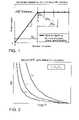
- FIG. 1is a graphical representation of ablation depth versus number of pulses for an exemplary via drilling.
- FIG. 2is a graphical representation of ⁇ N versus F/ ⁇ square root over ( ⁇ ) ⁇ for different values of the parameter L.
- FIGS. 3A and 3Bare optical micrographs that show cross sections of vias drilled in woven reinforced resin that exhibit respective small and large heat-affected zones.
- FIGS. 4A and 4Bare optical micrographs showing the results of processes to remove solder mask from pads that are approximately the same size as the laser beam being used to remove the solder mask.
- FIG. 5is a simplified schematic diagram of an exemplary laser system for processing low-k dielectric material supported on a substrate.
- FIG. 7is a simplified pictorial diagram of an optional imaged optics module that may be used in an exemplary laser system.
- Preferred embodimentsentail the use of a solid-state UV laser to perform via drilling and ablation of electronic circuit materials such as homogenous films, particulate-filled resins, polyimides, and fiber-reinforced polymers, with or without metal cladding.
- electronic circuit materialssuch as homogenous films, particulate-filled resins, polyimides, and fiber-reinforced polymers, with or without metal cladding.
- Some exemplary workpiecesinclude ABF® SH-9K, ABF® GX-3, ABF® GX-13, or similar products manufactured by other companies, but other via drilling target materials (including, but not limited to, multilayered, laminated substrates such as those used in high-density printed wiring boards and integrated circuit chip packages are also suitable for processing in accordance with the exemplary embodiments disclosed herein.
- Workpieces intended for via drillingtypically contain conductive cladding layers that may be positioned on the top or bottom surfaces of the workpiece. These layers may contain, for example, standard metals such as aluminium, copper, gold, molybdenum, nickel, palladium, platinum, silver, titanium, tungsten, metal nitrides, or combinations thereof. Conventional metal layers vary in thickness, typically between 5 and 36 ⁇ m (where 7.8 ⁇ 10 ⁇ 3 kg of metal equals a thickness of about 9 ⁇ m), but may be thinner, or as thick as 72 ⁇ m.
- the top and bottom conductive layersare typically made of the same material.
- a dielectric matrix or layer positioned between the conductive layersmay contain a standard organic dielectric material such as benzocyclobutane (BCB), bismaleimide triazine (BT), cardboard, cyanate esters, epoxies, phenolics, polyimides, polytetrafluorethylene (PTFE), various polymer alloys, or combinations thereof.
- BCBbenzocyclobutane
- BTbismaleimide triazine
- cardboardcyanate esters
- epoxiesphenolics
- polyimidespolyimides
- PTFEpolytetrafluorethylene
- Conventional organic dielectric layersvary considerably in thickness, but are typically much thicker than the conductive layers.
- An exemplary thickness range for the organic dielectric layersis about 30 to 400 ⁇ m.
- the dielectric layermay also contain a standard reinforcement component that may be fiber matte or dispersed particles of, for example, aramid fibers, ceramics, or glass woven or dispersed throughout the organic dielectric layer and that may comprise much of its thickness.
- Conventional reinforcement componentsare typically individual filaments or particles of about 1 to 10 ⁇ m and/or woven bundles of 10 ⁇ m to several hundreds of microns. Skilled persons will appreciate that the reinforcement components may be introduced as powders into the organic dielectrics and can be noncontiguous and nonuniform.
- Such composite or reinforced dielectric layerstypically require laser processing at a higher fluence than is needed to ablate unreinforced layers, but some particle-filled resins can be processed at a fluence similar to unreinforced layers.
- Some exemplary embodimentspertain to drilling blind vias, and particularly drilling blind vias in homogeneous or filled resins.
- Such blind via drillingis commonly done with a punching process, wherein sequential laser pulses are directed at a single target position on a workpiece until a desired depth is achieved such that the bottom copper layer is exposed.
- a total number of pulses N employed to form a qualified viaincludes a bulk number N 0 of bulk removal pulses for bulk material removal and a bottom surface cleaning number ⁇ N of cleaning pulses employed for cleaning off the bottom (metal) surface or pad of the via.
- the number of pulses to clean a bottom metal padcan take the significant portion of the total number of pulses required to drill the blind via if the laser pulsewidth is as long as several tens of nanoseconds.
- the bulk material removal and the bottom cleaninginvolve different laser/material interaction mechanisms. So one efficient way to reduce the via drilling time would be to reduce the bottom surface cleaning number ⁇ N of pulses used for bottom metal pad cleaning by adjusting laser parameters while somehow not adversely affecting the bulk material removal process.
- FIG. 1is a graphical representation of ablation depth versus number of pulses for an exemplary via drilling punching process using an imaged UV beam such that the total number of pulses N is partitioned into the bulk number N 0 of bulk removal pulses and the bottom surface cleaning number ⁇ N of cleaning pulses.
- FIG. 1shows that depending on the applications and the solid-state UV laser sources being used, the cleaning number ⁇ N of pulses for bottom pad cleaning can be significantly different as ⁇ N 1 , ⁇ N 2 , ⁇ N 3 , etc.
- the ratio of ⁇ N to N 0can be more than 1, meaning that more time is spent cleaning the bottom pad than for bulk material removal. So it is desirable to reduce ⁇ N in order to reduce the total drilling time per via. It is also desirable to reduce ⁇ N in order to reduce the amount of energy dumped into a pad to avoid unnecessary thermal damage.
- Conventional methods of controlling a via drilling processentail controlling the pulse energy for the given process.
- the pulse energy, E Pfor use in performing a given process is determined by the fluence, F, desired for the process.
- the fluence, in J/cm 2is calculated as
- Fthe pulse fluence in J/cm 2 and ⁇ is the laser pulsewidth in nanoseconds.
- C 1 and C 2are coefficients related to metal (pad) properties (such as optical, thermal, and/or mechanical properties) and where T m and T 0 are the melting temperature and the initial temperature of metal pad.
- FIG. 2is a graphical representation of ⁇ N versus F/ ⁇ square root over ( ⁇ ) ⁇ for different values of the parameter L for an exemplary via drilling punching process using an imaged UV beam.
- FIG. 2shows that when the term F/ ⁇ square root over ( ⁇ ) ⁇ is large enough, ⁇ N can be minimized to 1.
- ⁇ Ncan be predicted for different laser parameters.
- a solid-state UV laserhaving available laser power of 1.35 watts at the work surface at 50 kilohertz (kHz) to drill a via having a beam diameter of 58 ⁇ m, provides a fluence at the work surface of 1.02 J/cm 2 .
- the lower energy put into the target paddecreases the chances of thermal damage for small isolated target pads, which are not directly attached to a circuit trace and therefore cannot dispense of excess energy through a circuit trace.
- UV laser pulses having a pulsewidth shorter than 1,000 psemploy UV laser pulses having a pulsewidth shorter than 500 ps, and some embodiments employ UV laser pulses having a pulsewidth shorter than 100 ps. Pulsewidths shorter than 1 ps and particularly in the femtosecond regime may also be employed.
- FR4may be difficult to laser-machine for several reasons.
- the materialis highly heterogeneous, particularly with respect to properties governing laser ablation characteristics such as melting and vaporization temperatures.
- the vaporization temperatures of the woven glass reinforcement and the polymer resin matrixdiffer greatly.
- Pure silicon dioxidehas melting and vaporization temperatures of 1,970 Kelvin (K) and 2,503 K, respectively, while typical organic resins such as epoxies vaporize at much lower temperatures, on the order of 500 to 700 K. This disparity makes it difficult to laser-ablate the glass component while avoiding ablation of too much of the resin surrounding individual glass fibers or in regions directly adjacent to fiber bundles.
- FR4 glass clothis also woven from bundles or “yarns” of individual glass filaments. Filaments are typically 4 to 7 ⁇ m in diameter, and yarns range from about 50 ⁇ m to several hundred microns in diameter.
- the yarnsare generally woven in an open-weave pattern, resulting in areas of high glass density where yarns cross each other and areas of low or zero glass density, such as between adjacent bundles. Because the locations of vias cannot be selected a priori with respect to the weave pattern, the desirable via locations will vary with glass density. Thus laser micromachining process parameters that work equally well in both high- and low-glass-density regions of the substrate are desirable.
- the picosecond pulsewidth solid-state UV lasercan process the material with a smaller heat-affected zone and result in vias with better sidewall quality.
- FIGS. 3A and 3Bshow cross sections of through-hole vias drilled in woven reinforced resin that exhibit respective small and large heat-affected zones. Vias drilled with picosecond pulsewidth parameters may exhibit the smaller heat-affected zone similar to that shown in FIG. 3A and have less fiber protrusion on the sidewall of the via. This quality would be expected when drilling both blind vias and through-holes in this material in the picosecond pulsewidth regime.
- the increased fiber protrusion exhibited in FIG. 3Bcan be a consequence of a large heat-affected zone such as may be produced by parameters employing a tens of nanosecond pulsewidth regime.
- the picosecond pulsewidth solid-state UV laser processcan decrease the thermal diffusion of heat into the sidewalls of the via and result in improved via sidewall quality.
- the picosecond pulsewidth solid-state UV lasercan decrease the thermal diffusion of heat into the metal layer and result in better quality cutting and less chance of thermal damage to the metal layer, especially for thin metal layers.
- Laser machining green ceramicsposes concerns similar to those for processing FR4 due to the differences in the thermal properties of the organic binders and the ceramic microparticles.
- the disparity between the vaporization temperature of the binder (again, on the order of 500 K) and the ceramic (3,800 K for Al 2 O 3 )influences the way material is removed during laser drilling. Because ceramic has a high vaporization temperature, it is quite difficult to remove green ceramic through direct melting (at 2,340 K for Al 2 O 3 ) or vaporization of the microparticles.
- the preferred laser micromachining processinstead relies upon the explosive vaporization of the binder material holding the microparticles together.
- the bindervaporizes much more easily than the ceramic, and the organic vapor is driven to a high temperature at extremely high heating rates, creating localized high-pressure gas regions in the spaces between microparticles.
- the high-pressure gasthen expands rapidly, disintegrating the green ceramic material.
- the green ceramic materialcan be removed while in its solid state with each laser pulse, at removal rates much higher than could be obtained by its direct vaporization.
- Material removal by explosive vaporization of the bindercan be either advantageous or disadvantageous in laser micromachining green ceramics. If the organic vapor pressure is too high or spread across too wide an area, undesirable effects such as chipping or microcracking can occur. If the high-pressure regions are too localized or not hot enough, poor material-removal rates will result.
- the picosecond pulsewidth solid-state UV laser processcan decrease the thermal diffusion of heat into the sidewalls of the via and result in improved via sidewall quality in green ceramic materials.
- FIGS. 4A and 4Bare optical micrographs showing the results of processes to remove solder mask from pads that are approximately the same size as the laser beam being used to remove the solder mask.
- Solder maskis typically removed through time-consuming lithographic processes that may suffer from alignment constraints or through chemical etching processes, and can be difficult to process with typical solid-state laser techniques.
- liquid photoimageable solder maskLPISM
- DFSMdry film solder mask
- Typical available liquid photoimageable solder maskinclude, but are not limited to: Coates ImageCure XV501T & XV501TSM, Coates ImageFlex (Flexible Solder Mask) SV 601T, Enthone DSR 3241 and DSR 3241 GM, Rogers Rflex 8080 LP1 and Rflex 8080 LP3 (flexible), Taiyo PSR 4000 BN and 4000 AUS5, Taiyo PSR 9000 (Flexible), or Vantico Probimer 77 LPI Solder Mask.
- Typical available dry film solder maskinclude, but are not limited to: Dupont VACREL 8100, Dupont Flexible Photoimageable Coverlay (PIC) 1000 and 2000, Shipley (Dynachem) DynaMASK 5000, or Shipley ConforMASK 2500.
- the pad of the workpiece shown in FIG. 4Areceived too much energy during processing and delaminated from the panel.
- the pad of the workpiece shown in FIG. 4Bdid not receive excessive energy from the process, so delamination did not occur and the results are acceptable.
- the UV picosecond laser machining techniquecan be employed to remove any resist material with or without photosensitizers.
- Conventional photoresist materialsgenerally comprise positive photoresists that become soluble where exposed to light and negative photoresists that become polymerized (insoluble) where exposed to light.
- Photoresist materialsinclude, but are not limited to, Novolak (M Cresol formaldehyde) or an etch-resistant poly coating, such as polyisoprene or polymethylisopropenyl ketone.
- FIG. 5is a simplified schematic diagram of an exemplary laser system 10 for via formation or solder pad cleaning.
- the laser system 10preferably employs a high-average-power pulsed picosecond laser subsystem 14 that includes a dynamic laser pulse generator or oscillator module 12 and an amplification module 16 , such as a DPSS power amplifier.
- the dynamic laser pulse generator or oscillator module 12preferably employs a diode-pumped master oscillator to emit oscillator output pulses having a pulsewidth that is shorter than about 1,000 ps, preferably shorter than about 500 ps, and more preferably shorter than 100 ps, at a wavelength shorter than about 400 nanometers (nm), such as 266 nm, 351 nm, or 355 nm or other conventionally available solid-state or fiber laser UV harmonic wavelengths.
- the oscillator output pulsesare directed into the amplification module 16 .
- the amplification module 16may be a single-pass, multipass, or regenerative DPSS amplifier.
- the amplification module 16may be a diode-pumped rare-earth-doped silica fiber power amplifier.
- the amplification module 16may be a diode-pumped, rare-earth-doped silica photonic crystal fiber power amplifier.
- the oscillator module 12 and the amplification module 16preferably employ Nd-doped lasants as gain materials.
- a preferred Nd-doped lasantis Nd:GdVO 4 , but alternative Nd-doped lasants include, but are not limited to, Nd:YVO 4 , Nd:YLF, Nd:glass, and Nd:YAG.
- the oscillator module 12 and the amplification module 16may comprise the same or different lasants with the same or different doping concentrations.
- the oscillator module 12 and the amplification module 16also preferably employ frequency-selecting elements, prisms, filters, etalons, and/or other elements well known to skilled practitioners to preferentially produce gain at the desired wavelength.
- an external optical modulator 18such as an acousto-optic modulator (AOM) or an electro-optic modulator (EOM), can be triggered to provide laser output 20 a that may contain a single pulse, multiple independently triggered pulses, or bursts of pulses selected from a pulse train emitted from the amplification module 16 of the picosecond laser subsystem 14 .
- the laser pulses of the laser output 20 ahave high average power.
- the optical modulator 18may be triggered directly or indirectly by a system control computer 22 , subsystem interface electronics 24 , and/or a modulator control supply 26 as known to skilled practitioners.
- the trigger timingmay be coordinated, if desirable, with the control of a laser power supply 28 directly or indirectly by the system control computer 22 and/or the subsystem interface electronics 24 .
- Skilled personswill appreciate that useful AOM modulation techniques are disclosed in U.S. Pat. No. 7,019,891 of Johnson and can be employed in many embodiments. U.S. Pat. No. 7,019,891 is herein incorporated by reference.
- the oscillator module 12may comprise a pulsed semiconductor laser emitting picosecond pulses.
- the oscillator module 12may comprise a pulsed fiber master oscillator.
- An exemplary pulsed fiber master oscillatormay be a diode-pumped, Nd-doped or Yb-doped silica fiber master oscillator employing a SESAM. Skilled persons will appreciate that other rare-earth-doped fibers may alternatively be employed and that other mode-locking elements may alternatively be employed.
- the amplification module 16may be a diode-pumped, Yb-doped silica fiber master amplifier. In yet another exemplary embodiment, the amplification module 16 may be a diode-pumped, Nd-doped silica fiber power amplifier. Skilled persons will appreciate that other rare-earth-doped fibers may alternatively be employed for the amplification module 16 . Skilled persons will appreciate that fibers employing step index profiles, step index profiles incorporating polarization maintaining elements, or air gap profiles may be employed.
- the laser output 20 ais optionally passed through a variety of well-known expansion and/or collimation optics 42 , propagated along an optical path 20 , and directed by a beam-positioning system 30 to impinge laser system output pulse(s) 32 on a desired laser target position 34 on a workpiece 52 such as a PWB.
- An exemplary beam-positioning system 30may include a translation stage positioner that may employ at least two transverse stages 36 and 38 that support, for example, X, Y, and/or Z positioning mirrors 44 and permit quick movement between the target positions 34 on the same or different workpieces 52 .
- the translation stage positioneris a split-axis system in which a Y stage 36 , typically moved by linear motors along rails 46 , supports and moves the workpiece 52 , and an X stage 38 , typically moved by linear motors along rails 48 , supports and moves beam-positioning optics such as a fast positioner 50 and associated focusing lens(es) and/or other optics.
- the Z dimension between the X stage 38 and the Y stage 36may also be adjustable.
- the positioning mirrors 44align the optical path 20 through any turns between the laser subsystem 14 and the fast positioner 50 , which is positioned along the optical path 20 .
- the fast positioner 50may, for example, employ high-resolution linear motors, one or more galvanometer mirrors, fast-steering mirrors, and/or acousto-optic steering techniques that can effect unique or repetitive processing operations based on provided test or design data.
- the Y and X stages 36 and 38 and the fast positioner 50can be controlled and moved independently or coordinated to move together in response to panelized or unpanelized data.
- the fast positioner 50may also include or be associated with a vision system that can be aligned to one or more fiducials on the surface of the workpiece 52 .
- the beam-positioning system 30can employ conventional vision or beam-to-work alignment systems that work through a shared objective lens, or off-axis, with a separate camera, and that are well known to skilled practitioners.
- an HRVX vision boxemploying Freedom Library software in a beam-positioning system 30 sold by Electro Scientific Industries, Inc. of Portland, Oreg. is employed to perform alignment between the laser subsystem 14 and the target positions 34 on the workpiece 52 .
- Other suitable alignment systemsare commercially available.
- An exemplary alignment systemmay employ bright-field, on-axis illumination, particularly for specularly reflecting workpieces such as lapped or polished wafers, but dark-field illumination or a combination of dark-field illumination and bright-field illumination may be employed.
- the beam-positioning system 30may also employ an Abbe error-correction system such as that described in detail in U.S. Pat. No. 6,430,465 of Cutler, the relevant portions of which are herein incorporated by reference.
- beam-positioning system 30Many variations of the beam-positioning system 30 are well known to skilled practitioners, and some embodiments of the beam-positioning system 30 are described in detail in U.S. Pat. No. 5,751,585 of Cutler et al.
- the ESI Model 2700 or 5320 micromachining systems available from Electro Scientific Industries, Inc. of Portland, Oreg.are exemplary implementations of the beam-positioning system 30 .
- Other exemplary positioning systems, such as model series numbers 27xx, 43xx, 44xx, or 53xx, 55xx, 56xx, manufactured by Electro Scientific Industries, Inc. of Portland, Oreg.can also be employed.
- the positioning systemcan be programmed to utilize toolpath files that will dynamically position at high speeds the laser system output pulses 32 to produce a wide variety of useful via drilling patterns, which may be either periodic or nonperiodic. Skilled persons will also appreciate that AOM beam-steering techniques disclosed in U.S. Pat. No. 7,019,891 can be used in combination with or substituted for the fast positioner 50 and/or the beam-positioning system 30 .
- the laser output 20 amay also be directed through additional conventional system optical elements that may include, but are not limited to, nonlinear conversion optics 56 , optional correction optics 58 , and/or optional imaged optics module 62 , which may be employed to control the output power and shape the beam profile of the laser pulses received at the target or workpiece surface.
- Harmonic conversion techniquesemploying conventional nonlinear conversion optics 56 to convert a common fundamental wavelength to a second, third, fourth, or fifth harmonic wavelength are well known to skilled practitioners.
- the optional imaged optics module 62may include an optical element 64 , a lens 66 , and an aperture mask 68 placed at or near the beam waist created by the optical element 64 to block any undesirable side lobes and peripheral portions of the beam so that a precisely shaped spot profile is subsequently imaged onto the work surface.
- the optical element 64is a diffractive device or lens
- the lens 66is a collimating lens to add flexibility to the configuration of the laser system 10 .
- Varying the size of the aperture to match the properties of the optical element 64can control the edge sharpness of the spot profile to produce a size-specified, sharper-edged intensity profile that should enhance the alignment accuracy.
- the shape of the aperturecan be precisely circular or can be changed to rectangular, elliptical, or other noncircular shapes that can be aligned parallel or perpendicular to a cutting direction.
- the aperture mask 68may optionally be flared outwardly at its light-exiting side.
- the aperture mask 68 in the imaged optics module 62preferably comprises sapphire. Skilled persons will appreciate that the aperture mask 68 can be used without the optical element 64 and the lens 66 .
- optical element 64includes one or more beam-shaping components that convert laser pulses having a raw Gaussian irradiance profile into shaped (and focused) pulses that have a near-uniform “top hat” profile, or particularly a super-Gaussian irradiance profile, in proximity to the aperture mask 68 downstream of the optical element 64 .
- beam-shaping componentsmay include aspheric optics or diffractive optics.
- the lens 66comprises imaging optics useful for controlling beam size and divergence. Skilled persons will appreciate that a single imaging lens component or multiple lens components could be employed. Skilled persons will also appreciate, and it is preferred, that shaped laser output can be employed without using the aperture mask 68 .
- the beam-shaping componentsinclude a diffractive optic element (DOE) that can perform complex beam shaping with high efficiency and accuracy.
- DOEdiffractive optic element
- the beam-shaping componentsnot only transform the Gaussian irradiance profile to a near-uniform irradiance profile, but they also focus the shaped output to a determinable or specified spot size.
- the DOEmay include multiple separate elements such as the phase plate, and transform elements disclosed in U.S. Pat. No. 5,864,430 of Dickey et al., which also discloses techniques for designing DOEs for the purpose of beam shaping.
- the shaping and imaging techniques discussed aboveare described in detail in U.S. Pat. No. 6,433,301, the relevant portions of which are herein incorporated by reference.
- a laser power control module 70may be employed to achieve laser pulse power control by using modulation methods including, but not limited to, diode pump modulation or external modulation (such as with an external laser power controller 60 , including, but not limited to, AOMs or EOMs or motorized polarization rotation optics positioned along the optical path 20 ) or a combination thereof.
- one or more beam-detection devices 54such as photodiodes, may be downstream of the laser power controller 60 , such as aligned with a positioning mirror 44 that is adapted to be partly transmissive to the wavelength of the laser output 20 a .
- the beam-detection optics and electronicsmay be associated directly or indirectly with the laser power control module 70 , and/or may be directly or indirectly in communication with the system control computer 22 and/or the subsystem interface electronics 24 , and/or may be used to sample modulated laser output 20 a and generate correction signals to the modulators and/or other system optical elements to produce stable modulated output having parameters desirable for processing the workpiece 52 .
- Conventional power-control techniquesare known to skilled practitioners. Some exemplary AOM power-control techniques are disclosed in U.S. Pat. No. 7,019,891.
- Preferred pulse repetition frequencies employedrange from 50 kHz to 10 megahertz (MHz). In many cases, pulse repetition frequencies smaller than 1 MHz are preferred. Certain applications may, however, employ pulse repetition frequencies in the range from 10 MHz to 100 MHz. Typical focused spot sizes employed range from 10 ⁇ m to 100 ⁇ m. Certain applications may, however, employ spot sizes in the range from 1.5 ⁇ m to 10 ⁇ m.
- the laser parameters employed for pad cleaningmay also be used for bulk processing.
- the laser parameters for pad cleaningmay be different from those used for bulk cleaning.
- the fluence employed for bulk removalis maintained at about the value for pad cleaning, but the pulsewidth for pad cleaning is changed (significantly decreased) to decrease the number of pulses and decrease the amount of time employed for pad cleaning.
- Other laser parametersmay be changed as well between the bulk processing and pad cleaning steps. Such parameters may include, but are not limited to, wavelength, energy per pulse, repetition rate, or spot size.
- U.S. Pat. No. 5,841,099 of Owen et al. and U.S. Pat. No. 6,407,363 of Dunsky et al.which are herein incorporated by reference, disclose techniques for two-step, single-pass processing of blind and through-hole vias by employing a first set of laser parameters to process an overlying metal layer and a second set of laser parameters to process the bulk material.
- U.S. Pat. No. 5,841,099 of Owen et al.discloses changing (increasing) the repetition rate and/or changing (increasing) the spot size after processing the overlying metal layer so that the bulk material effectively receives less energy per pulse than the overlying metal layer.
- U.S. Pat. No. 6,407,363 of Dunsky et al.discloses focus- and spot-size-changing techniques employed to control the irradiance used to form the via in order to enhance via quality as well as to provide a single-pass, two-step method for processing the metal layer and then processing the bulk material. Such techniques can be accomplished with the use of a deformable mirror, but may also be accomplished with the use of an AOM.
- the techniques disclosedmay be employed to implement a three-step via drilling process such that different laser parameters are employed to process the overlying metal layer, to remove the bulk material, and to clean the pad.
- the metal layermay be processed at a first set of parameters, the repetition rate and/or spot size may be changed after the metal layer is removed to provide a second set of parameters, and then the pulsewidth may be decreased to provide a third set of parameters for cleaning the pad material.
- different wavelengthsmay be used for any of the steps. These changes may be implemented in a single laser or by two or more lasers.
- pad cleaning parametersneed not be constrained by typical fluence threshold limitations, because removal of a small amount of the underlying metal layer is acceptable and may be desirable to ensure that the pad surface is completely clean.
- the bulk material removal and the pad-cleaning processmay employ outward- or inward-spiraling or concentric-circle processing techniques or any variation of loop-profile processing techniques, such as those disclosed in U.S. Pat. No. 6,407,363 of Dunsky et al., whenever the via size or pad size is larger than the spot size.
- trepanning techniquescan be employed to create through-holes.
- typical bite sizesmay range from about 1 nm to about 15 ⁇ m.
- Typical scanning velocitiesmay range from about 10 to about 1,000 millimeters per second.
- a picosecond pulsewidth solid-state UV laserproduces steeper thermal gradients requiring less energy for cleaning the last remaining layer of material, solder mask, or resist material on the target pad. The lower energy put into the target pad results in more efficient processing and less chance of thermal damage for small isolated target pads.
- these laser output parameterscan decrease the thermal diffusion of heat into the sidewalls of the via, so sidewall quality is improved.
- the picosecond pulsewidth regimecan decrease the thermal diffusion of heat into the metal layer and result in better quality cutting and less chance of thermal damage to the metal layer, especially for thin metal layers.
Landscapes
- Engineering & Computer Science (AREA)
- Physics & Mathematics (AREA)
- Optics & Photonics (AREA)
- Plasma & Fusion (AREA)
- Mechanical Engineering (AREA)
- Manufacturing & Machinery (AREA)
- Microelectronics & Electronic Packaging (AREA)
- Electromagnetism (AREA)
- Laser Beam Processing (AREA)
- Printing Elements For Providing Electric Connections Between Printed Circuits (AREA)
- Electric Connection Of Electric Components To Printed Circuits (AREA)
Abstract
Description
where EPis the pulse energy in J and D is the beam spot diameter in cm. Applicants have found that drilling the same material at the same fluence level with lasers having different pulsewidths results in different quality for the bottom copper cladding layer of a target specimen. Applicants have determined that a more appropriate parameter for predicting the bottom copper cladding quality for blind vias is
where F is the pulse fluence in J/cm2and τ is the laser pulsewidth in nanoseconds.
where C1and C2are coefficients related to metal (pad) properties (such as optical, thermal, and/or mechanical properties) and where Tmand T0are the melting temperature and the initial temperature of metal pad.
Claims (32)
Priority Applications (9)
| Application Number | Priority Date | Filing Date | Title |
|---|---|---|---|
| US11/440,697US7605343B2 (en) | 2006-05-24 | 2006-05-24 | Micromachining with short-pulsed, solid-state UV laser |
| CN2007800178178ACN101448603B (en) | 2006-05-24 | 2007-05-21 | Method for improving laser through-hole drilling yield and clean surface and system thereof |
| PCT/US2007/069398WO2007140168A1 (en) | 2006-05-24 | 2007-05-21 | Micromachining with short-pulsed, solid-state uv laser |
| GB0822494AGB2452198A (en) | 2006-05-24 | 2007-05-21 | Micromachining with short-pulsed, solid-state UV laser |
| DE112007001246TDE112007001246T5 (en) | 2006-05-24 | 2007-05-21 | Micromachining with solid-state UV laser with short pulses |
| JP2009512248AJP5816409B2 (en) | 2006-05-24 | 2007-05-21 | Method to increase throughput for laser via drilling |
| KR1020087028552AKR101372437B1 (en) | 2006-05-24 | 2007-05-21 | Micromachining with short-pulsed, solid-state uv laser |
| TW096118342ATWI403379B (en) | 2006-05-24 | 2007-05-23 | Micromachining with short-pulsed, solid-state uv laser |
| US12/581,008US8415586B2 (en) | 2006-05-24 | 2009-10-16 | Method for increasing throughput of solder mask removal by minimizing the number of cleaning pulses |
Applications Claiming Priority (1)
| Application Number | Priority Date | Filing Date | Title |
|---|---|---|---|
| US11/440,697US7605343B2 (en) | 2006-05-24 | 2006-05-24 | Micromachining with short-pulsed, solid-state UV laser |
Related Child Applications (1)
| Application Number | Title | Priority Date | Filing Date |
|---|---|---|---|
| US12/581,008DivisionUS8415586B2 (en) | 2006-05-24 | 2009-10-16 | Method for increasing throughput of solder mask removal by minimizing the number of cleaning pulses |
Publications (2)
| Publication Number | Publication Date |
|---|---|
| US20070272667A1 US20070272667A1 (en) | 2007-11-29 |
| US7605343B2true US7605343B2 (en) | 2009-10-20 |
Family
ID=38748590
Family Applications (2)
| Application Number | Title | Priority Date | Filing Date |
|---|---|---|---|
| US11/440,697Active2027-08-17US7605343B2 (en) | 2006-05-24 | 2006-05-24 | Micromachining with short-pulsed, solid-state UV laser |
| US12/581,008Expired - Fee RelatedUS8415586B2 (en) | 2006-05-24 | 2009-10-16 | Method for increasing throughput of solder mask removal by minimizing the number of cleaning pulses |
Family Applications After (1)
| Application Number | Title | Priority Date | Filing Date |
|---|---|---|---|
| US12/581,008Expired - Fee RelatedUS8415586B2 (en) | 2006-05-24 | 2009-10-16 | Method for increasing throughput of solder mask removal by minimizing the number of cleaning pulses |
Country Status (8)
| Country | Link |
|---|---|
| US (2) | US7605343B2 (en) |
| JP (1) | JP5816409B2 (en) |
| KR (1) | KR101372437B1 (en) |
| CN (1) | CN101448603B (en) |
| DE (1) | DE112007001246T5 (en) |
| GB (1) | GB2452198A (en) |
| TW (1) | TWI403379B (en) |
| WO (1) | WO2007140168A1 (en) |
Cited By (13)
| Publication number | Priority date | Publication date | Assignee | Title |
|---|---|---|---|---|
| US20080061044A1 (en)* | 2006-09-11 | 2008-03-13 | Disco Corporation | Laser processing method and laser beam processing machine |
| US20080296273A1 (en)* | 2007-06-01 | 2008-12-04 | Electro Scientific Industries, Inc. | Method of and apparatus for laser drilling holes with improved taper |
| US20080296272A1 (en)* | 2007-05-31 | 2008-12-04 | Electro Scientific Industries, Inc. | Multiple laser wavelength and pulse width process drilling |
| US20100197116A1 (en)* | 2008-03-21 | 2010-08-05 | Imra America, Inc. | Laser-based material processing methods and systems |
| US8648277B2 (en) | 2011-03-31 | 2014-02-11 | Electro Scientific Industries, Inc. | Laser direct ablation with picosecond laser pulses at high pulse repetition frequencies |
| US9321126B2 (en) | 2004-03-31 | 2016-04-26 | Imra America, Inc. | Laser-based material processing apparatus and methods |
| TWI554176B (en)* | 2013-03-19 | 2016-10-11 | 天腦財富管理公司 | A device and a method for machining printed circuit boards |
| US9527159B2 (en) | 2013-03-15 | 2016-12-27 | Electro Scientific Industries, Inc. | Laser emission-based control of beam positioner |
| US20170120390A1 (en)* | 2015-10-30 | 2017-05-04 | Laser Systems Inc. | Manufacturing method of processed resin substrate and laser processing apparatus |
| US20180131069A1 (en)* | 2016-11-08 | 2018-05-10 | LGS Innovations LLC | Systems and methods of designing, tuning and producing ceramic filters |
| WO2019236616A1 (en) | 2018-06-05 | 2019-12-12 | Electro Scientific Industries, Inc. | Laser-processing apparatus, methods of operating the same, and methods of processing workpieces using the same |
| US10864599B2 (en) | 2016-03-17 | 2020-12-15 | Electro Scientific Industries, Inc. | Location of image plane in a laser processing system |
| US11077526B2 (en) | 2015-09-09 | 2021-08-03 | Electro Scientific Industries, Inc. | Laser processing apparatus, methods of laser-processing workpieces and related arrangements |
Families Citing this family (25)
| Publication number | Priority date | Publication date | Assignee | Title |
|---|---|---|---|---|
| US10307862B2 (en) | 2009-03-27 | 2019-06-04 | Electro Scientific Industries, Inc | Laser micromachining with tailored bursts of short laser pulses |
| US8604380B2 (en) | 2010-08-19 | 2013-12-10 | Electro Scientific Industries, Inc. | Method and apparatus for optimally laser marking articles |
| EA024987B8 (en) | 2011-06-01 | 2017-03-31 | Фиб-Сервисез Интеллекчуал С.А. | Method for manufacturing ceramic parts |
| PL2768626T3 (en) | 2011-09-23 | 2019-07-31 | Boegli-Gravures S.A. | Method and device for producing a structured surface on a steel embossing roller |
| EP2763812A4 (en)* | 2011-10-03 | 2016-04-20 | Electro Scient Ind Inc | Method and apparatus for optimally laser marking articles |
| KR20140138134A (en)* | 2012-02-28 | 2014-12-03 | 일렉트로 싸이언티픽 인더스트리이즈 인코포레이티드 | Method and apparatus for separation of strengthened glass and articles produced thereby |
| GB2511064A (en) | 2013-02-21 | 2014-08-27 | M Solv Ltd | Method of forming electrode structure for capacitive touch sensor |
| GB2514084B (en)* | 2013-02-21 | 2016-07-27 | M-Solv Ltd | Method of forming an electrode structure for capacitive touch sensor |
| CN104625416B (en)* | 2014-12-29 | 2016-06-22 | 北京理工大学 | Based on square hole auxiliary electron dynamic regulation crystal silicon surface periodic micro-nano structure method |
| JP6497301B2 (en)* | 2015-11-17 | 2019-04-10 | 株式会社デンソー | Manufacturing method of resin molding |
| JP2017112222A (en)* | 2015-12-16 | 2017-06-22 | 三菱瓦斯化学株式会社 | Laser drilling method |
| US11064611B2 (en)* | 2018-06-29 | 2021-07-13 | Ipg Photonics Corporation | Patterning and removal of circuit board material using ultrafast lasers |
| CN109396667A (en)* | 2018-07-06 | 2019-03-01 | 耀睦新材料科技(上海)有限公司 | A kind of laser micro-processing method of tungsten thin slice |
| WO2020115797A1 (en)* | 2018-12-03 | 2020-06-11 | 三菱電機株式会社 | Laser processing method and laser processing device |
| KR102265037B1 (en)* | 2019-04-12 | 2021-06-17 | 경북대학교 산학협력단 | Manufacturing method of microlens array and microlens array manufacturing system |
| CN111864030A (en)* | 2019-04-26 | 2020-10-30 | 诺沛半导体有限公司 | Light-emitting diode carrier board with arc laser window and its manufacturing method |
| US11509949B2 (en) | 2019-09-13 | 2022-11-22 | Disney Enterprises, Inc. | Packager for segmenter fluidity |
| CN113510393B (en)* | 2020-04-10 | 2023-08-18 | 大族激光科技产业集团股份有限公司 | Method for laser drilling of ceramic workpiece |
| DE102020007017B4 (en) | 2020-11-12 | 2022-10-06 | Hochschule Mittweida (Fh) | Method for removing dirt deposits on at least one geometric structure produced by means of microtechnology and/or nanotechnology of at least one body and using an ultra-short pulsed laser with pulses in burst mode |
| KR102477657B1 (en)* | 2021-03-18 | 2022-12-14 | 주식회사 이오테크닉스 | Laser drilling method |
| EP4088855B1 (en)* | 2021-03-30 | 2024-01-31 | The Boeing Company | Laser module end effector for robotic device |
| US11687012B2 (en)* | 2021-06-25 | 2023-06-27 | Taiwan Semiconductor Manufacturing Company, Ltd. | Reduce mask defect impact by contamination decompose |
| WO2024005097A1 (en)* | 2022-06-30 | 2024-01-04 | 太陽ホールディングス株式会社 | Method for manufacturing circuit board |
| WO2024005103A1 (en)* | 2022-06-30 | 2024-01-04 | 太陽ホールディングス株式会社 | Method for manufacturing circuit board |
| CN118543996B (en)* | 2024-05-30 | 2025-06-24 | 中南大学 | Ceramic material high-quality laser drilling method based on sandwich structure |
Citations (43)
| Publication number | Priority date | Publication date | Assignee | Title |
|---|---|---|---|---|
| US4914663A (en) | 1988-04-22 | 1990-04-03 | The Board Of Trustees Of Leland Stanford, Jr. University | Generation of short high peak power pulses from an injection mode-locked Q-switched laser oscillator |
| US4970553A (en)* | 1989-12-04 | 1990-11-13 | Xerox Corporation | Electrical component with conductive path |
| US5208437A (en) | 1990-05-18 | 1993-05-04 | Hitachi, Ltd. | Method of cutting interconnection pattern with laser and apparatus thereof |
| EP0666504A1 (en) | 1994-01-10 | 1995-08-09 | E.I. Du Pont De Nemours And Company | Aqueous photoimageable liquid emulsion, photoimageable film and process of manufacture |
| US5593606A (en) | 1994-07-18 | 1997-01-14 | Electro Scientific Industries, Inc. | Ultraviolet laser system and method for forming vias in multi-layered targets |
| US5656186A (en) | 1994-04-08 | 1997-08-12 | The Regents Of The University Of Michigan | Method for controlling configuration of laser induced breakdown and ablation |
| US5725914A (en) | 1992-09-03 | 1998-03-10 | Deutsche Forschungsanstalt fuer Luft - und Raumfahrt e.V. | Process and apparatus for producing a functional structure of a semiconductor component |
| US5742634A (en) | 1994-08-24 | 1998-04-21 | Imar Technology Co. | Picosecond laser |
| US5751585A (en) | 1995-03-20 | 1998-05-12 | Electro Scientific Industries, Inc. | High speed, high accuracy multi-stage tool positioning system |
| US5841099A (en) | 1994-07-18 | 1998-11-24 | Electro Scientific Industries, Inc. | Method employing UV laser pulses of varied energy density to form depthwise self-limiting blind vias in multilayered targets |
| US5864430A (en) | 1996-09-10 | 1999-01-26 | Sandia Corporation | Gaussian beam profile shaping apparatus, method therefor and evaluation thereof |
| US5965043A (en) | 1996-11-08 | 1999-10-12 | W. L. Gore & Associates, Inc. | Method for using ultrasonic treatment in combination with UV-lasers to enable plating of high aspect ratio micro-vias |
| JP2000202664A (en)* | 1999-01-08 | 2000-07-25 | Sumitomo Heavy Ind Ltd | Lasder drilling method |
| JP2000202679A (en)* | 1999-01-08 | 2000-07-25 | Sumitomo Heavy Ind Ltd | Laser beam piercing method and machine |
| US6169014B1 (en) | 1998-09-04 | 2001-01-02 | U.S. Philips Corporation | Laser crystallization of thin films |
| US6333485B1 (en) | 1998-12-11 | 2001-12-25 | International Business Machines Corporation | Method for minimizing sample damage during the ablation of material using a focused ultrashort pulsed beam |
| US20020040893A1 (en) | 2000-10-06 | 2002-04-11 | Hitachi Via Mechanics, Ltd. | Method and apparatus for drilling printed wiring boards |
| US6407363B2 (en) | 2000-03-30 | 2002-06-18 | Electro Scientific Industries, Inc. | Laser system and method for single press micromachining of multilayer workpieces |
| US6430465B2 (en) | 2000-01-11 | 2002-08-06 | Electro Scientific Industries, Inc. | Abbe error correction system and method |
| US6433301B1 (en) | 1999-05-28 | 2002-08-13 | Electro Scientific Industries, Inc. | Beam shaping and projection imaging with solid state UV Gaussian beam to form vias |
| US6479788B1 (en) | 1997-11-10 | 2002-11-12 | Hitachi Via Mechanics, Ltd. | Method and apparatus of making a hole in a printed circuit board |
| US20020170898A1 (en) | 2001-03-29 | 2002-11-21 | Ehrmann Jonathan S. | High-speed, precision, laser-based method and system for processing material of one or more targets within a field |
| US6541731B2 (en) | 2000-01-25 | 2003-04-01 | Aculight Corporation | Use of multiple laser sources for rapid, flexible machining and production of vias in multi-layered substrates |
| US6574250B2 (en) | 2000-01-10 | 2003-06-03 | Electro Scientific Industries, Inc. | Laser system and method for processing a memory link with a burst of laser pulses having ultrashort pulse widths |
| US20030102291A1 (en) | 2001-11-30 | 2003-06-05 | Xinbing Liu | System and method of laser drilling |
| US20030127500A1 (en) | 2002-01-08 | 2003-07-10 | International Business Machines Corporation | Method for forming solder connections on a circuitized substrate |
| US6610960B2 (en)* | 2001-05-23 | 2003-08-26 | Siemens Aktiengesellschaft | Method for drilling micro-holes with a laser beam |
| JP2003260579A (en)* | 2002-03-08 | 2003-09-16 | Sumitomo Heavy Ind Ltd | Method and device for laser beam machining |
| US6621040B1 (en) | 1996-01-11 | 2003-09-16 | The Regents Of The University Of California | Ultrashort pulse laser machining of metals and alloys |
| JP2003285176A (en)* | 2002-03-26 | 2003-10-07 | Sumitomo Heavy Ind Ltd | Laser beam machining method |
| JP2004074211A (en)* | 2002-08-15 | 2004-03-11 | Sumitomo Heavy Ind Ltd | Laser beam machining method |
| US6708404B1 (en)* | 1999-06-17 | 2004-03-23 | Mitsubishi Gas Chemical Company, Inc. | Method of producing high-density copper clad multi-layered printed wiring board having highly reliable through hole |
| US6727458B2 (en) | 1999-12-28 | 2004-04-27 | Gsi Lumonics, Inc. | Energy-efficient, laser-based method and system for processing target material |
| US6734387B2 (en) | 1999-05-27 | 2004-05-11 | Spectra Physics Lasers, Inc. | Method and apparatus for micro-machining of articles that include polymeric materials |
| US6750422B2 (en)* | 1998-03-18 | 2004-06-15 | Mitsubishi Gas Chemical Company, Inc. | Method of making through hole with laser, copper-clad laminate suitable for making hole, and auxiliary material for making hole |
| US6784399B2 (en) | 2001-05-09 | 2004-08-31 | Electro Scientific Industries, Inc. | Micromachining with high-energy, intra-cavity Q-switched CO2 laser pulses |
| US6809291B1 (en) | 2002-08-30 | 2004-10-26 | Southeastern Universities Research Assn., Inc. | Process for laser machining and surface treatment |
| JP2004344961A (en)* | 2003-05-26 | 2004-12-09 | Sumitomo Heavy Ind Ltd | Method for making hole |
| US20050175385A1 (en)* | 2003-11-05 | 2005-08-11 | Samsung Electro-Mechanics Co., Ltd. | Method of producing printed circuit board with embedded resistor |
| US20050265408A1 (en) | 2004-05-28 | 2005-12-01 | Weisheng Lei | Method of providing consistent quality of target material removal by lasers having different output performance characteristics |
| US6979798B2 (en) | 2003-03-07 | 2005-12-27 | Gsi Lumonics Corporation | Laser system and method for material processing with ultra fast lasers |
| US7019891B2 (en) | 2004-06-07 | 2006-03-28 | Electro Scientific Industries, Inc. | AOM modulation techniques employing plurality of tilt-angled transducers to improve laser system performance |
| US7057133B2 (en) | 2004-04-14 | 2006-06-06 | Electro Scientific Industries, Inc. | Methods of drilling through-holes in homogenous and non-homogenous substrates |
Family Cites Families (11)
| Publication number | Priority date | Publication date | Assignee | Title |
|---|---|---|---|---|
| US2005A (en)* | 1841-03-16 | Improvement in the manner of constructing molds for casting butt-hinges | ||
| DE19544929C2 (en)* | 1995-12-01 | 2001-02-15 | Fraunhofer Ges Forschung | Device for the flux-free application of a solder to a substrate or a chip |
| US7576909B2 (en)* | 1998-07-16 | 2009-08-18 | Imra America, Inc. | Multimode amplifier for amplifying single mode light |
| EP1219150B1 (en)* | 1999-09-30 | 2003-03-05 | Siemens Aktiengesellschaft | Method and device for laser drilling laminates |
| TWI226814B (en)* | 1999-12-16 | 2005-01-11 | Matsushita Electric Industrial Co Ltd | A removable film, a substrate with film, a process for forming the removable film and a process for the manufacturing of the circuit board |
| US6340806B1 (en)* | 1999-12-28 | 2002-01-22 | General Scanning Inc. | Energy-efficient method and system for processing target material using an amplified, wavelength-shifted pulse train |
| CN1344131A (en)* | 2000-09-18 | 2002-04-10 | 华通电脑股份有限公司 | Laser Drilling Method for Printed Circuit Board and Substrate |
| JP2003101188A (en)* | 2001-09-26 | 2003-04-04 | Nitto Denko Corp | Method for forming via hole, flexible wiring board using the same, and method for manufacturing the same |
| US20050087522A1 (en)* | 2003-10-24 | 2005-04-28 | Yunlong Sun | Laser processing of a locally heated target material |
| SG114754A1 (en)* | 2004-02-25 | 2005-09-28 | Kulicke & Soffa Investments | Laser cleaning system for a wire bonding machine |
| US8116341B2 (en) | 2007-05-31 | 2012-02-14 | Electro Scientific Industries, Inc. | Multiple laser wavelength and pulse width process drilling |
- 2006
- 2006-05-24USUS11/440,697patent/US7605343B2/enactiveActive
- 2007
- 2007-05-21GBGB0822494Apatent/GB2452198A/ennot_activeWithdrawn
- 2007-05-21KRKR1020087028552Apatent/KR101372437B1/ennot_activeExpired - Fee Related
- 2007-05-21JPJP2009512248Apatent/JP5816409B2/ennot_activeExpired - Fee Related
- 2007-05-21WOPCT/US2007/069398patent/WO2007140168A1/enactiveApplication Filing
- 2007-05-21CNCN2007800178178Apatent/CN101448603B/ennot_activeExpired - Fee Related
- 2007-05-21DEDE112007001246Tpatent/DE112007001246T5/ennot_activeWithdrawn
- 2007-05-23TWTW096118342Apatent/TWI403379B/ennot_activeIP Right Cessation
- 2009
- 2009-10-16USUS12/581,008patent/US8415586B2/ennot_activeExpired - Fee Related
Patent Citations (43)
| Publication number | Priority date | Publication date | Assignee | Title |
|---|---|---|---|---|
| US4914663A (en) | 1988-04-22 | 1990-04-03 | The Board Of Trustees Of Leland Stanford, Jr. University | Generation of short high peak power pulses from an injection mode-locked Q-switched laser oscillator |
| US4970553A (en)* | 1989-12-04 | 1990-11-13 | Xerox Corporation | Electrical component with conductive path |
| US5208437A (en) | 1990-05-18 | 1993-05-04 | Hitachi, Ltd. | Method of cutting interconnection pattern with laser and apparatus thereof |
| US5725914A (en) | 1992-09-03 | 1998-03-10 | Deutsche Forschungsanstalt fuer Luft - und Raumfahrt e.V. | Process and apparatus for producing a functional structure of a semiconductor component |
| EP0666504A1 (en) | 1994-01-10 | 1995-08-09 | E.I. Du Pont De Nemours And Company | Aqueous photoimageable liquid emulsion, photoimageable film and process of manufacture |
| US5656186A (en) | 1994-04-08 | 1997-08-12 | The Regents Of The University Of Michigan | Method for controlling configuration of laser induced breakdown and ablation |
| US5593606A (en) | 1994-07-18 | 1997-01-14 | Electro Scientific Industries, Inc. | Ultraviolet laser system and method for forming vias in multi-layered targets |
| US5841099A (en) | 1994-07-18 | 1998-11-24 | Electro Scientific Industries, Inc. | Method employing UV laser pulses of varied energy density to form depthwise self-limiting blind vias in multilayered targets |
| US5742634A (en) | 1994-08-24 | 1998-04-21 | Imar Technology Co. | Picosecond laser |
| US5751585A (en) | 1995-03-20 | 1998-05-12 | Electro Scientific Industries, Inc. | High speed, high accuracy multi-stage tool positioning system |
| US6621040B1 (en) | 1996-01-11 | 2003-09-16 | The Regents Of The University Of California | Ultrashort pulse laser machining of metals and alloys |
| US5864430A (en) | 1996-09-10 | 1999-01-26 | Sandia Corporation | Gaussian beam profile shaping apparatus, method therefor and evaluation thereof |
| US5965043A (en) | 1996-11-08 | 1999-10-12 | W. L. Gore & Associates, Inc. | Method for using ultrasonic treatment in combination with UV-lasers to enable plating of high aspect ratio micro-vias |
| US6479788B1 (en) | 1997-11-10 | 2002-11-12 | Hitachi Via Mechanics, Ltd. | Method and apparatus of making a hole in a printed circuit board |
| US6750422B2 (en)* | 1998-03-18 | 2004-06-15 | Mitsubishi Gas Chemical Company, Inc. | Method of making through hole with laser, copper-clad laminate suitable for making hole, and auxiliary material for making hole |
| US6169014B1 (en) | 1998-09-04 | 2001-01-02 | U.S. Philips Corporation | Laser crystallization of thin films |
| US6333485B1 (en) | 1998-12-11 | 2001-12-25 | International Business Machines Corporation | Method for minimizing sample damage during the ablation of material using a focused ultrashort pulsed beam |
| JP2000202664A (en)* | 1999-01-08 | 2000-07-25 | Sumitomo Heavy Ind Ltd | Lasder drilling method |
| JP2000202679A (en)* | 1999-01-08 | 2000-07-25 | Sumitomo Heavy Ind Ltd | Laser beam piercing method and machine |
| US6734387B2 (en) | 1999-05-27 | 2004-05-11 | Spectra Physics Lasers, Inc. | Method and apparatus for micro-machining of articles that include polymeric materials |
| US6433301B1 (en) | 1999-05-28 | 2002-08-13 | Electro Scientific Industries, Inc. | Beam shaping and projection imaging with solid state UV Gaussian beam to form vias |
| US6708404B1 (en)* | 1999-06-17 | 2004-03-23 | Mitsubishi Gas Chemical Company, Inc. | Method of producing high-density copper clad multi-layered printed wiring board having highly reliable through hole |
| US6727458B2 (en) | 1999-12-28 | 2004-04-27 | Gsi Lumonics, Inc. | Energy-efficient, laser-based method and system for processing target material |
| US6574250B2 (en) | 2000-01-10 | 2003-06-03 | Electro Scientific Industries, Inc. | Laser system and method for processing a memory link with a burst of laser pulses having ultrashort pulse widths |
| US6430465B2 (en) | 2000-01-11 | 2002-08-06 | Electro Scientific Industries, Inc. | Abbe error correction system and method |
| US6541731B2 (en) | 2000-01-25 | 2003-04-01 | Aculight Corporation | Use of multiple laser sources for rapid, flexible machining and production of vias in multi-layered substrates |
| US6407363B2 (en) | 2000-03-30 | 2002-06-18 | Electro Scientific Industries, Inc. | Laser system and method for single press micromachining of multilayer workpieces |
| US20020040893A1 (en) | 2000-10-06 | 2002-04-11 | Hitachi Via Mechanics, Ltd. | Method and apparatus for drilling printed wiring boards |
| US20020170898A1 (en) | 2001-03-29 | 2002-11-21 | Ehrmann Jonathan S. | High-speed, precision, laser-based method and system for processing material of one or more targets within a field |
| US6784399B2 (en) | 2001-05-09 | 2004-08-31 | Electro Scientific Industries, Inc. | Micromachining with high-energy, intra-cavity Q-switched CO2 laser pulses |
| US6610960B2 (en)* | 2001-05-23 | 2003-08-26 | Siemens Aktiengesellschaft | Method for drilling micro-holes with a laser beam |
| US20030102291A1 (en) | 2001-11-30 | 2003-06-05 | Xinbing Liu | System and method of laser drilling |
| US20030127500A1 (en) | 2002-01-08 | 2003-07-10 | International Business Machines Corporation | Method for forming solder connections on a circuitized substrate |
| JP2003260579A (en)* | 2002-03-08 | 2003-09-16 | Sumitomo Heavy Ind Ltd | Method and device for laser beam machining |
| JP2003285176A (en)* | 2002-03-26 | 2003-10-07 | Sumitomo Heavy Ind Ltd | Laser beam machining method |
| JP2004074211A (en)* | 2002-08-15 | 2004-03-11 | Sumitomo Heavy Ind Ltd | Laser beam machining method |
| US6809291B1 (en) | 2002-08-30 | 2004-10-26 | Southeastern Universities Research Assn., Inc. | Process for laser machining and surface treatment |
| US6979798B2 (en) | 2003-03-07 | 2005-12-27 | Gsi Lumonics Corporation | Laser system and method for material processing with ultra fast lasers |
| JP2004344961A (en)* | 2003-05-26 | 2004-12-09 | Sumitomo Heavy Ind Ltd | Method for making hole |
| US20050175385A1 (en)* | 2003-11-05 | 2005-08-11 | Samsung Electro-Mechanics Co., Ltd. | Method of producing printed circuit board with embedded resistor |
| US7057133B2 (en) | 2004-04-14 | 2006-06-06 | Electro Scientific Industries, Inc. | Methods of drilling through-holes in homogenous and non-homogenous substrates |
| US20050265408A1 (en) | 2004-05-28 | 2005-12-01 | Weisheng Lei | Method of providing consistent quality of target material removal by lasers having different output performance characteristics |
| US7019891B2 (en) | 2004-06-07 | 2006-03-28 | Electro Scientific Industries, Inc. | AOM modulation techniques employing plurality of tilt-angled transducers to improve laser system performance |
Non-Patent Citations (5)
| Title |
|---|
| International Preliminary Report (Nov. 27, 2008) and Written Opinion of International Searching Authority concerning the corresponding International Pat. Appl. No. PCT/US2007/069398. |
| Lapczyna (Ultra high repetition rate (133 MHz) laser ablation . . . . |
| Machine translation of Japan Patent No. 2003-285,176, Jun. 2009.* |
| Search Report and Written Opinion of Korean International Searching Authority (Oct. 31, 2007) concerning the corresponding International Pat. Appl. No. PCT/US2007/069398. |
| U.S. Appl. No. 11/756,507, filed May 31, 2007 of Lei et al. |
Cited By (22)
| Publication number | Priority date | Publication date | Assignee | Title |
|---|---|---|---|---|
| US9321126B2 (en) | 2004-03-31 | 2016-04-26 | Imra America, Inc. | Laser-based material processing apparatus and methods |
| US7842902B2 (en)* | 2006-09-11 | 2010-11-30 | Disco Corporation | Laser processing method and laser beam processing machine |
| US20080061044A1 (en)* | 2006-09-11 | 2008-03-13 | Disco Corporation | Laser processing method and laser beam processing machine |
| US8116341B2 (en)* | 2007-05-31 | 2012-02-14 | Electro Scientific Industries, Inc. | Multiple laser wavelength and pulse width process drilling |
| US20080296272A1 (en)* | 2007-05-31 | 2008-12-04 | Electro Scientific Industries, Inc. | Multiple laser wavelength and pulse width process drilling |
| US8710402B2 (en) | 2007-06-01 | 2014-04-29 | Electro Scientific Industries, Inc. | Method of and apparatus for laser drilling holes with improved taper |
| US20080296273A1 (en)* | 2007-06-01 | 2008-12-04 | Electro Scientific Industries, Inc. | Method of and apparatus for laser drilling holes with improved taper |
| US20100197116A1 (en)* | 2008-03-21 | 2010-08-05 | Imra America, Inc. | Laser-based material processing methods and systems |
| US8158493B2 (en) | 2008-03-21 | 2012-04-17 | Imra America, Inc. | Laser-based material processing methods and systems |
| US8785813B2 (en) | 2008-03-21 | 2014-07-22 | Imra America, Inc. | Laser-based material processing methods and systems |
| US8648277B2 (en) | 2011-03-31 | 2014-02-11 | Electro Scientific Industries, Inc. | Laser direct ablation with picosecond laser pulses at high pulse repetition frequencies |
| US9527159B2 (en) | 2013-03-15 | 2016-12-27 | Electro Scientific Industries, Inc. | Laser emission-based control of beam positioner |
| TWI554176B (en)* | 2013-03-19 | 2016-10-11 | 天腦財富管理公司 | A device and a method for machining printed circuit boards |
| US11077526B2 (en) | 2015-09-09 | 2021-08-03 | Electro Scientific Industries, Inc. | Laser processing apparatus, methods of laser-processing workpieces and related arrangements |
| US20170120390A1 (en)* | 2015-10-30 | 2017-05-04 | Laser Systems Inc. | Manufacturing method of processed resin substrate and laser processing apparatus |
| US11338393B2 (en)* | 2015-10-30 | 2022-05-24 | Laser Systems Inc. | Manufacturing method of processed resin substrate and laser processing apparatus |
| US20220241901A1 (en)* | 2015-10-30 | 2022-08-04 | Laser Systems Inc. | Manufacturing method of processed resin substrate and laser processing apparatus |
| US10864599B2 (en) | 2016-03-17 | 2020-12-15 | Electro Scientific Industries, Inc. | Location of image plane in a laser processing system |
| US20180131069A1 (en)* | 2016-11-08 | 2018-05-10 | LGS Innovations LLC | Systems and methods of designing, tuning and producing ceramic filters |
| US10587030B2 (en)* | 2016-11-08 | 2020-03-10 | LGS Innovations LLC | Systems and methods of designing, tuning and producing ceramic filters |
| WO2019236616A1 (en) | 2018-06-05 | 2019-12-12 | Electro Scientific Industries, Inc. | Laser-processing apparatus, methods of operating the same, and methods of processing workpieces using the same |
| US12011785B2 (en) | 2018-06-05 | 2024-06-18 | Electro Scientific Industries, Inc. | Laser-processing apparatus, methods of operating the same, and methods of processing workpieces using the same |
Also Published As
| Publication number | Publication date |
|---|---|
| CN101448603B (en) | 2013-12-18 |
| TW200804023A (en) | 2008-01-16 |
| GB0822494D0 (en) | 2009-01-14 |
| JP5816409B2 (en) | 2015-11-18 |
| US20070272667A1 (en) | 2007-11-29 |
| DE112007001246T5 (en) | 2009-06-04 |
| US20100032417A1 (en) | 2010-02-11 |
| KR20090013798A (en) | 2009-02-05 |
| JP2009538539A (en) | 2009-11-05 |
| TWI403379B (en) | 2013-08-01 |
| US8415586B2 (en) | 2013-04-09 |
| GB2452198A (en) | 2009-02-25 |
| WO2007140168A1 (en) | 2007-12-06 |
| CN101448603A (en) | 2009-06-03 |
| KR101372437B1 (en) | 2014-03-11 |
Similar Documents
| Publication | Publication Date | Title |
|---|---|---|
| US7605343B2 (en) | Micromachining with short-pulsed, solid-state UV laser | |
| CN112091421B (en) | Laser processing apparatus, method of laser processing a workpiece and related arrangements | |
| US7528342B2 (en) | Method and apparatus for via drilling and selective material removal using an ultrafast pulse laser | |
| US9321126B2 (en) | Laser-based material processing apparatus and methods | |
| KR101866579B1 (en) | Method and apparatus for drilling using a series of laser pulses | |
| US20050087522A1 (en) | Laser processing of a locally heated target material | |
| US5841099A (en) | Method employing UV laser pulses of varied energy density to form depthwise self-limiting blind vias in multilayered targets | |
| US8116341B2 (en) | Multiple laser wavelength and pulse width process drilling | |
| KR100952530B1 (en) | Laser based system for memory link processing using picosecond laser | |
| KR20090026137A (en) | Laser treatment of materials containing low-k dielectric materials | |
| JP2009512553A (en) | Synthetic pulse repetition rate machining for dual-head laser micromachining systems | |
| JP2005518945A (en) | Laser processing method | |
| KR100504234B1 (en) | Laser drilling method | |
| JP2000202664A (en) | Lasder drilling method | |
| JP2002126886A (en) | Laser perforating device | |
| JP2008284577A (en) | Method of laser beam machining, flexible printed circuit board | |
| JP2002331378A (en) | Laser beam machining method | |
| JP3245820B2 (en) | Laser drilling method | |
| JP2005007440A (en) | Laser beam machining method and laser beam machining machine | |
| Murai et al. | Development of a laser processing technology for high thermal radiation multilayer module |
Legal Events
| Date | Code | Title | Description |
|---|---|---|---|
| AS | Assignment | Owner name:ELECTRO SCIENTIFIC INDUSTRIES, INC., OREGON Free format text:ASSIGNMENT OF ASSIGNORS INTEREST;ASSIGNORS:LEI, WEISHENG;SIMENSON, GLENN;MATSUMOTO, HISASHI;AND OTHERS;REEL/FRAME:021860/0828;SIGNING DATES FROM 20081106 TO 20081119 | |
| AS | Assignment | Owner name:ELECTRO SCIENTIFIC INDUSTRIES, INC., OREGON Free format text:ASSIGNMENT OF ASSIGNORS INTEREST;ASSIGNORS:LEI, WEISHENG;SIMENSON, GLENN;MATSUMOTO, HISASHI;AND OTHERS;REEL/FRAME:022084/0784;SIGNING DATES FROM 20081106 TO 20081119 | |
| STCF | Information on status: patent grant | Free format text:PATENTED CASE | |
| CC | Certificate of correction | ||
| FPAY | Fee payment | Year of fee payment:4 | |
| REMI | Maintenance fee reminder mailed | ||
| FEPP | Fee payment procedure | Free format text:7.5 YR SURCHARGE - LATE PMT W/IN 6 MO, LARGE ENTITY (ORIGINAL EVENT CODE: M1555) | |
| MAFP | Maintenance fee payment | Free format text:PAYMENT OF MAINTENANCE FEE, 8TH YEAR, LARGE ENTITY (ORIGINAL EVENT CODE: M1552) Year of fee payment:8 | |
| AS | Assignment | Owner name:BARCLAYS BANK PLC, AS COLLATERAL AGENT, NEW YORK Free format text:PATENT SECURITY AGREEMENT (TERM LOAN);ASSIGNORS:ELECTRO SCIENTIFIC INDUSTRIES, INC.;MKS INSTRUMENTS, INC.;NEWPORT CORPORATION;REEL/FRAME:048211/0227 Effective date:20190201 Owner name:BARCLAYS BANK PLC, AS COLLATERAL AGENT, NEW YORK Free format text:PATENT SECURITY AGREEMENT (ABL);ASSIGNORS:ELECTRO SCIENTIFIC INDUSTRIES, INC.;MKS INSTRUMENTS, INC.;NEWPORT CORPORATION;REEL/FRAME:048211/0312 Effective date:20190201 | |
| AS | Assignment | Owner name:BARCLAYS BANK PLC, AS COLLATERAL AGENT, NEW YORK Free format text:CORRECTIVE ASSIGNMENT TO CORRECT THE REMOVE U.S. PATENT NO. 7,919,646 PREVIOUSLY RECORDED ON REEL 048211 FRAME 0227. ASSIGNOR(S) HEREBY CONFIRMS THE PATENT SECURITY AGREEMENT (TERM LOAN);ASSIGNORS:ELECTRO SCIENTIFIC INDUSTRIES, INC.;MKS INSTRUMENTS, INC.;NEWPORT CORPORATION;REEL/FRAME:055006/0492 Effective date:20190201 Owner name:BARCLAYS BANK PLC, AS COLLATERAL AGENT, NEW YORK Free format text:CORRECTIVE ASSIGNMENT TO CORRECT THE REMOVE U.S. PATENT NO.7,919,646 PREVIOUSLY RECORDED ON REEL 048211 FRAME 0312. ASSIGNOR(S) HEREBY CONFIRMS THE PATENT SECURITY AGREEMENT (ABL);ASSIGNORS:ELECTRO SCIENTIFIC INDUSTRIES, INC.;MKS INSTRUMENTS, INC.;NEWPORT CORPORATION;REEL/FRAME:055668/0687 Effective date:20190201 | |
| MAFP | Maintenance fee payment | Free format text:PAYMENT OF MAINTENANCE FEE, 12TH YEAR, LARGE ENTITY (ORIGINAL EVENT CODE: M1553); ENTITY STATUS OF PATENT OWNER: LARGE ENTITY Year of fee payment:12 | |
| AS | Assignment | Owner name:JPMORGAN CHASE BANK, N.A., AS COLLATERAL AGENT, ILLINOIS Free format text:SECURITY INTEREST;ASSIGNORS:MKS INSTRUMENTS, INC.;NEWPORT CORPORATION;ELECTRO SCIENTIFIC INDUSTRIES, INC.;REEL/FRAME:061572/0069 Effective date:20220817 | |
| AS | Assignment | Owner name:ELECTRO SCIENTIFIC INDUSTRIES, INC., OREGON Free format text:RELEASE BY SECURED PARTY;ASSIGNOR:BARCLAYS BANK PLC;REEL/FRAME:063009/0001 Effective date:20220817 Owner name:NEWPORT CORPORATION, MASSACHUSETTS Free format text:RELEASE BY SECURED PARTY;ASSIGNOR:BARCLAYS BANK PLC;REEL/FRAME:063009/0001 Effective date:20220817 Owner name:MKS INSTRUMENTS, INC., MASSACHUSETTS Free format text:RELEASE BY SECURED PARTY;ASSIGNOR:BARCLAYS BANK PLC;REEL/FRAME:063009/0001 Effective date:20220817 Owner name:ELECTRO SCIENTIFIC INDUSTRIES, INC., OREGON Free format text:RELEASE BY SECURED PARTY;ASSIGNOR:BARCLAYS BANK PLC;REEL/FRAME:062739/0001 Effective date:20220817 Owner name:NEWPORT CORPORATION, MASSACHUSETTS Free format text:RELEASE BY SECURED PARTY;ASSIGNOR:BARCLAYS BANK PLC;REEL/FRAME:062739/0001 Effective date:20220817 Owner name:MKS INSTRUMENTS, INC., MASSACHUSETTS Free format text:RELEASE BY SECURED PARTY;ASSIGNOR:BARCLAYS BANK PLC;REEL/FRAME:062739/0001 Effective date:20220817 |