US7601571B2 - Methods of manufacturing interferometric modulators with thin film transistors - Google Patents
Methods of manufacturing interferometric modulators with thin film transistorsDownload PDFInfo
- Publication number
- US7601571B2 US7601571B2US11/837,140US83714007AUS7601571B2US 7601571 B2US7601571 B2US 7601571B2US 83714007 AUS83714007 AUS 83714007AUS 7601571 B2US7601571 B2US 7601571B2
- Authority
- US
- United States
- Prior art keywords
- interferometric modulator
- semiconductor circuit
- film semiconductor
- layer
- manufacturing
- Prior art date
- Legal status (The legal status is an assumption and is not a legal conclusion. Google has not performed a legal analysis and makes no representation as to the accuracy of the status listed.)
- Expired - Lifetime, expires
Links
Images


Classifications
- G—PHYSICS
- G02—OPTICS
- G02B—OPTICAL ELEMENTS, SYSTEMS OR APPARATUS
- G02B26/00—Optical devices or arrangements for the control of light using movable or deformable optical elements
- G02B26/001—Optical devices or arrangements for the control of light using movable or deformable optical elements based on interference in an adjustable optical cavity
- G—PHYSICS
- G02—OPTICS
- G02B—OPTICAL ELEMENTS, SYSTEMS OR APPARATUS
- G02B26/00—Optical devices or arrangements for the control of light using movable or deformable optical elements
- G02B26/08—Optical devices or arrangements for the control of light using movable or deformable optical elements for controlling the direction of light
- G02B26/0816—Optical devices or arrangements for the control of light using movable or deformable optical elements for controlling the direction of light by means of one or more reflecting elements
- G02B26/0833—Optical devices or arrangements for the control of light using movable or deformable optical elements for controlling the direction of light by means of one or more reflecting elements the reflecting element being a micromechanical device, e.g. a MEMS mirror, DMD
- G02B26/0841—Optical devices or arrangements for the control of light using movable or deformable optical elements for controlling the direction of light by means of one or more reflecting elements the reflecting element being a micromechanical device, e.g. a MEMS mirror, DMD the reflecting element being moved or deformed by electrostatic means
Definitions
- Interferometric modulatorssuch as the iMoDTM modulate light by controlling the self-interference of light that strikes the front surface of the modulator.
- These types of modulatorstypically employ a cavity having at least one movable or deflectable wall. This deflectable wall moves through planes parallel to the front wall of the cavity-the wall that is first encountered by light striking the front surface of the modulator.
- the movable walltypically comprised at least partly of metal and highly reflective, moves towards the front surface of the cavity, self-interference of the light within the cavity occurs, and the varying distance between the front and movable wall affects the color of light that exits the cavity at the front surface.
- the front surfaceis typically the surface where the image seen by the viewer appears, as interferometric modulators are usually direct-view devices.
- the movable wallmoves in response to an actuation signal generated by addressing circuitry that sends the signal to the movable element.
- the addressing circuitryis generally manufactured off-chip from the array of movable elements. This is in part because the substrate upon which the interferometric modulators are manufactured is transparent, such as plastic or glass.
- Thin film transistorsmay be manufactured on transparent substrates. Integrating thin film transistors with the interferometric modulator array may provide an interferometric modulator with extended functionality.
- a method of manufacturing an interferometric modulator with thin film semiconductor circuit componentscomprises depositing a material layer over a transparent substrate, and patterning and etching the first material to form a portion of at least one interferometric modulator element and a portion of at least one thin film semiconductor circuit component.
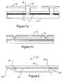
- FIGS. 1 a and 1 bshow embodiments of an interferometric modulator.
- FIG. 2shows a side view of an interferometric modulator having integrated thin film transistors.
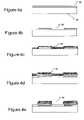
- FIGS. 3 a - 3 lshow embodiments of an integrated process flow for thin film transistors.
- FIGS. 4 a - 4 hshow embodiments of an integrated process flow for an interferometric modulator with thin film transistors.
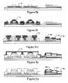
- FIGS. 5 a - 5 rshow embodiments of an integrated process flow for an interferometric modulator having low-temperature polysilicon, top gate transistors.
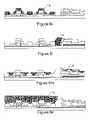
- FIGS. 6 a - 6 nshow embodiments of an integrated process flow for an interferometric modulator having low-temperature polysilicon, bottom gate transistors.
- FIG. 7shows a flowchart of an embodiment of a method to manufacture interferometric modulators in series with manufacture of polysilicon, top gate transistors.
- FIGS. 1 a and 1 bshow alternative embodiments of an interferometric modulator.
- interferometric modulatorsemploy a cavity having at least one movable or deflectable wall.
- the wall 20 of FIG. 1 atypically comprised at least partly of metal, moves towards a front surface 12 of the cavity, interference occurs that affects the color of light viewed at the front surface.
- the front surfaceis typically the surface where the image seen by the viewer appears, as the iMoD is a direct-view device.
- the front surface 12may have a stack of materials that form the optical stack 14 , also referred to as the first mirror.
- the movable wall 20is offset from the optical stack by a post 16 .
- the movable element 20is part of a membrane that covers the posts 16 , with a slightly elevated portion of the membrane 18 .
- the movable element 24is suspended over the cavity by the supports 22 that also form the posts.
- one iMoD elementmight correspond to one pixel.
- three iMoD elementsmay make up each pixel, one each for red, green and blue.
- the individual iMoD elementsare controlled separately to produce the desired pixel reflectivity.
- a voltageis applied to the movable wall, or element, of the cavity, causing it be to electrostatically attracted to the front surface that in turn affects the color of the pixel seen by the viewer.
- the addressing circuitrywill generally include transistors, with one or more transistors corresponding to each element on the modulator array. Currently, the transistors are manufactured off-chip from the modulator element. However, with the use of thin-film transistors, it is possible to manufacture the transistors on the substrate. In addition, as most MEMS devices may be manufactured from thin films, it is possible to integrate the manufacture of thin film transistors with the manufacture of MEMS devices.
- FIG. 2shows a side view of an interferometric modulator device.
- the modulatorhas an array of individually controlled, movable elements such as 30 , manufactured on the transparent substrate 10 .
- the modulator arrayis enclosed with a back plate 28 .
- Regions 32 a and 32 dare ‘outside’ the modulator, where the term ‘outside’ refers to being on the opposite side of the back plate or other packaging structure from the modulator array. This would not typically be where the transistors would go. The possibility of damaging the transistor leads between the modulator elements and the transistors with the back plate mounting processes may be too great.
- the transistorswould be manufactured directly adjacent the modulator array, where directly adjacent means that they are manufactured on portions of the substrate not used for the modulator array, but inside the back plate. Regions 32 b and 32 c are examples of such a location.
- the transistorsmay be manufactured side by side with the modulator elements, such as one transistor next to each element.
- the modulator arrayis manufactured on the ‘back’ of the transparent substrate 10 .
- the transparent substrateis shown ‘upside down’ from the view of FIG. 2 .
- the manufacture of the modulatorwill appear to be on top of the substrate.
- a first material layer 42has been deposited. This material may be used to form the gates for the thin film transistors and the optical stack of the interferometric modulator, as shown in FIG. 4 a.
- the first materialmay be metal.
- the first materialhas been patterned and etched to remove selected portions such as 44 of the material. This can form the gates of the transistors.
- the optical stack for the modulatorsmay be formed into rows as shown in FIG. 4 b.
- a first oxide layer 46has been deposited.
- the material used for the oxidemay be the same material used to form the optical stack dielectric for the modulators and the gate oxide for the transistors, shown in FIG. 4 c.
- the selection of the material for the oxidecan be adjusted for both the operation of the modulator and for compatibility with the further processes used to form the elements. For example, it is useful if the oxide material used is optically transparent for use in the modulator.
- a first sacrificial layeris deposited for the modulators. This layer will be etched to form the cavity, after the formation of other parts of the modulator is completed.
- the sacrificial layer 48 of FIG. 4 dmay actually be formed from two layers, a first layer of amorphous silicon and then a doped layer of amorphous silicon, as shown at 48 a and 48 b of FIG. 3 d.
- the use of amorphous silicon and doped amorphous silicon as the sacrificial layeris compatible with the processing of the modulator, and is used in the processing of the thin film transistors.
- the dielectric layer 46may be selected to be compatible with further processing, so the dielectric/oxide would be selected to be compatible with amorphous silicon.
- the sacrificial layeris patterned and etched to form post holes similar to 50 for the modulator elements, as shown in FIG. 4 e. Since the sacrificial layer is the amorphous silicon and doped amorphous silicon in one embodiment, this is also patterned and etched as part of the transistor formation process. Posts may be formed out of the same material used to planarize the thin film transistor structures such as polymer 52 in FIGS. 3 f and 4 f. Currently, the posts of the modulators are formed from a metal layer, either the metal of the membrane of FIG. 1 a or the metal of the supports of FIG. 1 b. However, there is no requirement to use metal for the posts. Using a polymer allows the planarization of the transistors to be done in parallel with the formation of the posts. An example of a polymer would be polyimide.
- FIG. 3 gappears similar to FIG. 3 f because the processing performed is not seen by the side view.
- the planarization layerwould be patterned and etched to clear the transistor leads. This clears the way for the metal contacts to be made with the deposition of the metal layer 54 in FIGS. 3 h and 4 g.
- This metalforms the mirror layer 20 in FIG. 1 a and the mirror element 24 in FIG. 1 b. It will also form the sources and drain electrodes for the transistors.
- the metal layer 54is the mirror layer and the mechanical layer, the layer that moves.
- the layer 54is the mirror layer and the post layer 52 is the mechanical layer.
- the metal layer 54is patterned and etched to form the source and drain electrodes as well as form the individual movable elements for the modulator in FIGS. 3 i.
- the gap 56is formed by the etching process performed on the metal layer.
- the doped amorphous silicon layer 48 ais then etched again in FIG. 3 j, using the source/drain electrode metal as a mask, to form the channel for the transistors. There is no equivalent process for the modulator element for this or the remaining transistor processes.
- FIGS. 3 k and 3 lThe final two processes for the transistor formation are show in FIGS. 3 k and 3 l.
- a passivation layer 60is deposited for the transistors.
- the passivation layeris etched to clear leads, such as by the gap show at 62 .
- the passivation layeris oxide.
- the transistor processingis then completed, upon which a release etch is performed to form gap 57 in FIG. 4 h, allowing the modulator elements to move freely. In this manner, the manufacture of thin film transistors is accomplished nearly in parallel with the manufacture of a thin film, interferometric spatial light modulator.
- a second sacrificial layerwould be deposited, followed by a second metal layer.
- the patterning and etching of the metal layer to form the support posts and then the etching of the sacrificial layer to free up the elementsmay be performed after the formation of the thin film transistors.
- the alteration of the processing for the architecture of FIG. 1 bis more clearly set out in U.S. patent application Ser. No. 10/644,312, filed Aug. 19, 2003, “Separable Modulator Architecture.”
- the process of manufacturing the thin film transistorsis compatible with the manufacture of either architecture of the interferometric modulator array.
- the manufacture of the transistorsmay use low-temperature polysilicon, either in a top gate or a bottom gate structure.
- These processeswill be demonstrated with the separable modulator architecture of FIG. 1 b, but could also apply to the architecture of FIG. 1 a.
- the selection of the modulator architectureis independent of the selection of the type of transistors used, and the integration process is adaptable to the different, possible combinations.
- FIGS. 5 a - 5 rshow embodiments of a process flow for a top-gate, low-temperature, polysilicon transistor flow integrated with the process flow for an interferometric modulator.
- the transistor flow and the modulator floware shown side-by-side on what appears to be the same portion of the substrate, but that is just for ease of demonstration and is not intended to imply any particular location for the modulator array relative to the transistor array.
- the optical stack 42is deposited on the substrate 40 .
- the oxide 46 and the first portion 48 a of the first sacrificial layer 48is deposited, masked and etched. If FIG. 5 c, the second portion 48 b is deposited.
- the layersare patterned and etched to form the basic structures for the modulator as well as the transistors. The structure to the right of the diagram is one element of an interferometric modulator array, used to show the integration of the two process flows.
- the n-channel mask for the transistoris deposited to allow for n-channel doping.
- a gate oxide 60is then deposited.
- the oxideis then patterned and etched to obtain the resulting structures in FIG. 5 f.
- the second portion 48 b of the sacrificial layerhas been patterned and etched to form underlying structures for the modulator element.
- the gate molybdenumis deposited at 66 . This is patterned and etched to form the structures such as 66 a and 66 b in FIG. 5 i.
- the p source and drainare doped using a mask, resulting in doped p source and drain 68 .
- a similar processis performed for the n source and drain 70 in FIG. 5 k.
- the interlayer dielectric 72is deposited over the transistor structures. No comparable processes are being performed on the modulator element at this point.
- the mirror layer 54is deposited to be used by the transistors as the source/drain contacts, and the modulator as the mirrors 54 a, 54 b and 54 c. This resumes the integrated processing flow.
- a sacrificial layer 74is deposited, which will provide support for the mirror supports and then be removed to allow the mirror elements to move freely. The sacrificial layer 74 will not be used by any transistor processes, but the transistors may require that the material remain compatible with the processes in the transistor flow.
- the sacrificial layer 74has been cleared from the transistor region and has been patterned and etched to form post holes 50 a, 50 b and 50 c.
- a planarization layer 76is deposited in FIG. 5 p.
- the mechanical layer 52is then deposited in FIG. 5 q to form the support posts for the mirrors.
- the transistor regionthen received a passivation layer in FIG. 5 r.
- FIGS. 6 a - 6 nshow similar processes as FIGS. 5 a -S r, but for a bottom gate, low-temperature, polysilicon transistor array. Similar structures and layers use the same reference numbers between the two for easier comparison.
- the optical stack 42 for the modulatoris deposited on the substrate 40 .
- the two portions of the first sacrificial layer 48are deposited, patterned and etch in FIG. 6 b to form underlying structures for the modulator.
- the gate metal 80is deposited, patterned and etch and then the oxidation layer 82 is formed.
- the gate oxideis deposited in FIG. 6 d.
- the mirror layer 54is deposited, patterned and etched to form the mirrors form the modulator element, mirrors 54 a, 54 b and 54 c.
- the sacrificial layer 74is deposited, and FIG. 6 g, the post holes such as 5 a is formed, with sacrificial islands of layer 74 left on the transistor structures.
- an oxide layeris deposited and then patterned and etched to form oxide caps for the transistor structures.
- the n-type source and drainare doped as shown by 70
- the p-type source and drainare doped as shown by 68 in FIG. 6 j.
- the interlayer dielectric 72is deposited in FIG. 6 k.
- the planarization layer 76is deposited in FIG. 6 l.
- the mechanical layer 52is deposited that forms the posts in the post holes, and provides the source/drain contact metal for the transistors.
- the passivation layer 78is deposited.
- a process flowmay be provided that integrates the manufacturing of the transistors and the interferometric modulator on one substrate.
- This integrated process flowsaves processing steps, thereby reducing costs, and allows for faster processing of the devices. Faster processing of the device increases the output of devices, thereby also reducing costs.
- circuit component processingis performed first, then the processing for the interferometric modulator.
- orderingis switched.
- An example of the circuit component being manufactured firstis shown in FIG. 7 . The process starts with the transparent substrate.
- the optical stackis formed by deposition, patterning and etching of the electrode layer, the optical layer and the dielectric.
- the structures formed at covered with a protective oxide layerare formed at this point, the process flow concentrates on manufacture of the thin film circuit components.
- the componentis a top gate, low-temperature, polysilicon transistor.
- the amorphous siliconis deposited at 94 , with p-channel doping occurring at 96 , and n-channel doping at 98 .
- the gate oxide and metalare deposited at 100 , and the gate masked and etched at 102 . It must be noted that several processes have been; compressed for ease of discussion. The more detailed descriptions of these processes can be found in the discussion with regard to FIGS. 3-6 .
- the p-type source and drainare formed at 104 , and the corresponding n-type source and drain are formed at 106 .
- the interlayer dielectricis deposited at 108 , and the contacts are masked and etched to clear them at 10 .
- the source and drain metalis deposited and etched. Passivation of the circuit component occurs at 122 , with the contacts being cleared of the passivation material at 124 . At this point, the circuit component processing has been substantially completed.
- the protective oxide previously depositedis cleared and the interferometric modulator manufacture process begins.
- the modulatorcould be manufactured first and then the circuit component. A similar flow would occur for the circuit component, regardless of whether it is top or bottom gate, low-temperature polysilicon, other types of thin film transistors, or thin film diodes.
Landscapes
- Physics & Mathematics (AREA)
- General Physics & Mathematics (AREA)
- Optics & Photonics (AREA)
- Spectroscopy & Molecular Physics (AREA)
- Mechanical Light Control Or Optical Switches (AREA)
- Micromachines (AREA)
- Control Of Indicators Other Than Cathode Ray Tubes (AREA)
Abstract
Description
Claims (9)
Priority Applications (1)
| Application Number | Priority Date | Filing Date | Title |
|---|---|---|---|
| US11/837,140US7601571B2 (en) | 2004-07-02 | 2007-08-10 | Methods of manufacturing interferometric modulators with thin film transistors |
Applications Claiming Priority (2)
| Application Number | Priority Date | Filing Date | Title |
|---|---|---|---|
| US10/883,902US7256922B2 (en) | 2004-07-02 | 2004-07-02 | Interferometric modulators with thin film transistors |
| US11/837,140US7601571B2 (en) | 2004-07-02 | 2007-08-10 | Methods of manufacturing interferometric modulators with thin film transistors |
Related Parent Applications (1)
| Application Number | Title | Priority Date | Filing Date |
|---|---|---|---|
| US10/883,902DivisionUS7256922B2 (en) | 2004-07-02 | 2004-07-02 | Interferometric modulators with thin film transistors |
Publications (2)
| Publication Number | Publication Date |
|---|---|
| US20070275491A1 US20070275491A1 (en) | 2007-11-29 |
| US7601571B2true US7601571B2 (en) | 2009-10-13 |
Family
ID=35056906
Family Applications (2)
| Application Number | Title | Priority Date | Filing Date |
|---|---|---|---|
| US10/883,902Expired - LifetimeUS7256922B2 (en) | 2004-07-02 | 2004-07-02 | Interferometric modulators with thin film transistors |
| US11/837,140Expired - LifetimeUS7601571B2 (en) | 2004-07-02 | 2007-08-10 | Methods of manufacturing interferometric modulators with thin film transistors |
Family Applications Before (1)
| Application Number | Title | Priority Date | Filing Date |
|---|---|---|---|
| US10/883,902Expired - LifetimeUS7256922B2 (en) | 2004-07-02 | 2004-07-02 | Interferometric modulators with thin film transistors |
Country Status (8)
| Country | Link |
|---|---|
| US (2) | US7256922B2 (en) |
| EP (2) | EP1774393A2 (en) |
| CN (1) | CN1977206B (en) |
| AU (1) | AU2005270186A1 (en) |
| BR (1) | BRPI0512810A (en) |
| IL (1) | IL179983A0 (en) |
| TW (1) | TWI279919B (en) |
| WO (1) | WO2006014247A2 (en) |
Cited By (7)
| Publication number | Priority date | Publication date | Assignee | Title |
|---|---|---|---|---|
| US20100110526A1 (en)* | 2004-09-27 | 2010-05-06 | Qualcomm Mems Technologies, Inc. | Method and device for multistate interferometric light modulation |
| WO2011130715A2 (en) | 2010-04-16 | 2011-10-20 | Flex Lighting Ii, Llc | Illumination device comprising a film-based lightguide |
| WO2011130718A2 (en) | 2010-04-16 | 2011-10-20 | Flex Lighting Ii, Llc | Front illumination device comprising a film-based lightguide |
| US8928967B2 (en) | 1998-04-08 | 2015-01-06 | Qualcomm Mems Technologies, Inc. | Method and device for modulating light |
| US8971675B2 (en) | 2006-01-13 | 2015-03-03 | Qualcomm Mems Technologies, Inc. | Interconnect structure for MEMS device |
| US8988760B2 (en) | 2008-07-17 | 2015-03-24 | Qualcomm Mems Technologies, Inc. | Encapsulated electromechanical devices |
| US9110289B2 (en) | 1998-04-08 | 2015-08-18 | Qualcomm Mems Technologies, Inc. | Device for modulating light with multiple electrodes |
Families Citing this family (99)
| Publication number | Priority date | Publication date | Assignee | Title |
|---|---|---|---|---|
| US6674562B1 (en)* | 1994-05-05 | 2004-01-06 | Iridigm Display Corporation | Interferometric modulation of radiation |
| US7460291B2 (en)* | 1994-05-05 | 2008-12-02 | Idc, Llc | Separable modulator |
| US7907319B2 (en) | 1995-11-06 | 2011-03-15 | Qualcomm Mems Technologies, Inc. | Method and device for modulating light with optical compensation |
| TWI289708B (en) | 2002-12-25 | 2007-11-11 | Qualcomm Mems Technologies Inc | Optical interference type color display |
| US7417782B2 (en)* | 2005-02-23 | 2008-08-26 | Pixtronix, Incorporated | Methods and apparatus for spatial light modulation |
| US7342705B2 (en)* | 2004-02-03 | 2008-03-11 | Idc, Llc | Spatial light modulator with integrated optical compensation structure |
| US7706050B2 (en)* | 2004-03-05 | 2010-04-27 | Qualcomm Mems Technologies, Inc. | Integrated modulator illumination |
| US7256922B2 (en)* | 2004-07-02 | 2007-08-14 | Idc, Llc | Interferometric modulators with thin film transistors |
| US7561323B2 (en)* | 2004-09-27 | 2009-07-14 | Idc, Llc | Optical films for directing light towards active areas of displays |
| US7553684B2 (en) | 2004-09-27 | 2009-06-30 | Idc, Llc | Method of fabricating interferometric devices using lift-off processing techniques |
| US7405861B2 (en) | 2004-09-27 | 2008-07-29 | Idc, Llc | Method and device for protecting interferometric modulators from electrostatic discharge |
| US7355780B2 (en)* | 2004-09-27 | 2008-04-08 | Idc, Llc | System and method of illuminating interferometric modulators using backlighting |
| US7310179B2 (en)* | 2004-09-27 | 2007-12-18 | Idc, Llc | Method and device for selective adjustment of hysteresis window |
| US7349141B2 (en)* | 2004-09-27 | 2008-03-25 | Idc, Llc | Method and post structures for interferometric modulation |
| US7710636B2 (en) | 2004-09-27 | 2010-05-04 | Qualcomm Mems Technologies, Inc. | Systems and methods using interferometric optical modulators and diffusers |
| US7630123B2 (en)* | 2004-09-27 | 2009-12-08 | Qualcomm Mems Technologies, Inc. | Method and device for compensating for color shift as a function of angle of view |
| US20060132383A1 (en)* | 2004-09-27 | 2006-06-22 | Idc, Llc | System and method for illuminating interferometric modulator display |
| US7807488B2 (en)* | 2004-09-27 | 2010-10-05 | Qualcomm Mems Technologies, Inc. | Display element having filter material diffused in a substrate of the display element |
| US7668415B2 (en)* | 2004-09-27 | 2010-02-23 | Qualcomm Mems Technologies, Inc. | Method and device for providing electronic circuitry on a backplate |
| US7750886B2 (en) | 2004-09-27 | 2010-07-06 | Qualcomm Mems Technologies, Inc. | Methods and devices for lighting displays |
| US20060066586A1 (en)* | 2004-09-27 | 2006-03-30 | Gally Brian J | Touchscreens for displays |
| US7710632B2 (en)* | 2004-09-27 | 2010-05-04 | Qualcomm Mems Technologies, Inc. | Display device having an array of spatial light modulators with integrated color filters |
| US7508571B2 (en)* | 2004-09-27 | 2009-03-24 | Idc, Llc | Optical films for controlling angular characteristics of displays |
| US20060065622A1 (en)* | 2004-09-27 | 2006-03-30 | Floyd Philip D | Method and system for xenon fluoride etching with enhanced efficiency |
| US7373026B2 (en) | 2004-09-27 | 2008-05-13 | Idc, Llc | MEMS device fabricated on a pre-patterned substrate |
| US8310442B2 (en) | 2005-02-23 | 2012-11-13 | Pixtronix, Inc. | Circuits for controlling display apparatus |
| US8519945B2 (en) | 2006-01-06 | 2013-08-27 | Pixtronix, Inc. | Circuits for controlling display apparatus |
| US7304785B2 (en) | 2005-02-23 | 2007-12-04 | Pixtronix, Inc. | Display methods and apparatus |
| US9087486B2 (en) | 2005-02-23 | 2015-07-21 | Pixtronix, Inc. | Circuits for controlling display apparatus |
| US8482496B2 (en)* | 2006-01-06 | 2013-07-09 | Pixtronix, Inc. | Circuits for controlling MEMS display apparatus on a transparent substrate |
| US9261694B2 (en)* | 2005-02-23 | 2016-02-16 | Pixtronix, Inc. | Display apparatus and methods for manufacture thereof |
| US7999994B2 (en) | 2005-02-23 | 2011-08-16 | Pixtronix, Inc. | Display apparatus and methods for manufacture thereof |
| US9082353B2 (en) | 2010-01-05 | 2015-07-14 | Pixtronix, Inc. | Circuits for controlling display apparatus |
| US9229222B2 (en) | 2005-02-23 | 2016-01-05 | Pixtronix, Inc. | Alignment methods in fluid-filled MEMS displays |
| US20070205969A1 (en) | 2005-02-23 | 2007-09-06 | Pixtronix, Incorporated | Direct-view MEMS display devices and methods for generating images thereon |
| US7405852B2 (en)* | 2005-02-23 | 2008-07-29 | Pixtronix, Inc. | Display apparatus and methods for manufacture thereof |
| US7746529B2 (en) | 2005-02-23 | 2010-06-29 | Pixtronix, Inc. | MEMS display apparatus |
| US7304786B2 (en)* | 2005-02-23 | 2007-12-04 | Pixtronix, Inc. | Methods and apparatus for bi-stable actuation of displays |
| US20060209012A1 (en)* | 2005-02-23 | 2006-09-21 | Pixtronix, Incorporated | Devices having MEMS displays |
| US20080158635A1 (en)* | 2005-02-23 | 2008-07-03 | Pixtronix, Inc. | Display apparatus and methods for manufacture thereof |
| US8159428B2 (en) | 2005-02-23 | 2012-04-17 | Pixtronix, Inc. | Display methods and apparatus |
| US9158106B2 (en) | 2005-02-23 | 2015-10-13 | Pixtronix, Inc. | Display methods and apparatus |
| KR101375337B1 (en) | 2005-07-22 | 2014-03-18 | 퀄컴 엠이엠에스 테크놀로지스, 인크. | Electomechanical devices having support structures and methods of fabricating the same |
| EP1928780A2 (en) | 2005-09-30 | 2008-06-11 | Qualcomm Mems Technologies, Inc. | Mems device and interconnects for same |
| US7630114B2 (en) | 2005-10-28 | 2009-12-08 | Idc, Llc | Diffusion barrier layer for MEMS devices |
| KR100744543B1 (en)* | 2005-12-08 | 2007-08-01 | 한국전자통신연구원 | Micro-electro mechanical systems switch and method of fabricating the same switch |
| US7652814B2 (en) | 2006-01-27 | 2010-01-26 | Qualcomm Mems Technologies, Inc. | MEMS device with integrated optical element |
| US7603001B2 (en)* | 2006-02-17 | 2009-10-13 | Qualcomm Mems Technologies, Inc. | Method and apparatus for providing back-lighting in an interferometric modulator display device |
| US8526096B2 (en) | 2006-02-23 | 2013-09-03 | Pixtronix, Inc. | Mechanical light modulators with stressed beams |
| US7450295B2 (en)* | 2006-03-02 | 2008-11-11 | Qualcomm Mems Technologies, Inc. | Methods for producing MEMS with protective coatings using multi-component sacrificial layers |
| US8004743B2 (en)* | 2006-04-21 | 2011-08-23 | Qualcomm Mems Technologies, Inc. | Method and apparatus for providing brightness control in an interferometric modulator (IMOD) display |
| US7876489B2 (en)* | 2006-06-05 | 2011-01-25 | Pixtronix, Inc. | Display apparatus with optical cavities |
| US7766498B2 (en) | 2006-06-21 | 2010-08-03 | Qualcomm Mems Technologies, Inc. | Linear solid state illuminator |
| US7566664B2 (en) | 2006-08-02 | 2009-07-28 | Qualcomm Mems Technologies, Inc. | Selective etching of MEMS using gaseous halides and reactive co-etchants |
| US7845841B2 (en) | 2006-08-28 | 2010-12-07 | Qualcomm Mems Technologies, Inc. | Angle sweeping holographic illuminator |
| EP1943551A2 (en) | 2006-10-06 | 2008-07-16 | Qualcomm Mems Technologies, Inc. | Light guide |
| EP1943555B1 (en) | 2006-10-06 | 2012-05-02 | QUALCOMM MEMS Technologies, Inc. | Optical loss structure integrated in an illumination apparatus of a display |
| US7855827B2 (en)* | 2006-10-06 | 2010-12-21 | Qualcomm Mems Technologies, Inc. | Internal optical isolation structure for integrated front or back lighting |
| US8107155B2 (en)* | 2006-10-06 | 2012-01-31 | Qualcomm Mems Technologies, Inc. | System and method for reducing visual artifacts in displays |
| EP1958010A2 (en)* | 2006-10-10 | 2008-08-20 | Qualcomm Mems Technologies, Inc | Display device with diffractive optics |
| US7629197B2 (en) | 2006-10-18 | 2009-12-08 | Qualcomm Mems Technologies, Inc. | Spatial light modulator |
| EP2080045A1 (en) | 2006-10-20 | 2009-07-22 | Pixtronix Inc. | Light guides and backlight systems incorporating light redirectors at varying densities |
| US7864395B2 (en) | 2006-10-27 | 2011-01-04 | Qualcomm Mems Technologies, Inc. | Light guide including optical scattering elements and a method of manufacture |
| US7706042B2 (en) | 2006-12-20 | 2010-04-27 | Qualcomm Mems Technologies, Inc. | MEMS device and interconnects for same |
| US7852546B2 (en) | 2007-10-19 | 2010-12-14 | Pixtronix, Inc. | Spacers for maintaining display apparatus alignment |
| US9176318B2 (en) | 2007-05-18 | 2015-11-03 | Pixtronix, Inc. | Methods for manufacturing fluid-filled MEMS displays |
| US7777954B2 (en)* | 2007-01-30 | 2010-08-17 | Qualcomm Mems Technologies, Inc. | Systems and methods of providing a light guiding layer |
| US7733439B2 (en)* | 2007-04-30 | 2010-06-08 | Qualcomm Mems Technologies, Inc. | Dual film light guide for illuminating displays |
| US7719752B2 (en) | 2007-05-11 | 2010-05-18 | Qualcomm Mems Technologies, Inc. | MEMS structures, methods of fabricating MEMS components on separate substrates and assembly of same |
| US8929741B2 (en)* | 2007-07-30 | 2015-01-06 | Hewlett-Packard Development Company, L.P. | Optical interconnect |
| US7570415B2 (en) | 2007-08-07 | 2009-08-04 | Qualcomm Mems Technologies, Inc. | MEMS device and interconnects for same |
| US7949213B2 (en) | 2007-12-07 | 2011-05-24 | Qualcomm Mems Technologies, Inc. | Light illumination of displays with front light guide and coupling elements |
| US8068710B2 (en) | 2007-12-07 | 2011-11-29 | Qualcomm Mems Technologies, Inc. | Decoupled holographic film and diffuser |
| US20090168459A1 (en)* | 2007-12-27 | 2009-07-02 | Qualcomm Incorporated | Light guide including conjugate film |
| US8780704B2 (en)* | 2008-01-10 | 2014-07-15 | Qualcomm Incorporated | Shared resource allocation |
| FR2926635B1 (en)* | 2008-01-21 | 2012-08-03 | Silios Technologies | WAVELENGTH SPECTROSCOPY DEVICE WITH INTEGRATED FILTERS |
| US7863079B2 (en) | 2008-02-05 | 2011-01-04 | Qualcomm Mems Technologies, Inc. | Methods of reducing CD loss in a microelectromechanical device |
| WO2009102733A2 (en)* | 2008-02-12 | 2009-08-20 | Qualcomm Mems Technologies, Inc. | Integrated front light diffuser for reflective displays |
| WO2009102731A2 (en) | 2008-02-12 | 2009-08-20 | Qualcomm Mems Technologies, Inc. | Devices and methods for enhancing brightness of displays using angle conversion layers |
| US7944604B2 (en) | 2008-03-07 | 2011-05-17 | Qualcomm Mems Technologies, Inc. | Interferometric modulator in transmission mode |
| WO2009126745A2 (en)* | 2008-04-11 | 2009-10-15 | Qualcomm Mems Technologies, Inc. | Method for improving pv aesthetics and efficiency |
| US8248560B2 (en)* | 2008-04-18 | 2012-08-21 | Pixtronix, Inc. | Light guides and backlight systems incorporating prismatic structures and light redirectors |
| WO2009129264A1 (en) | 2008-04-15 | 2009-10-22 | Qualcomm Mems Technologies, Inc. | Light with bi-directional propagation |
| US7719754B2 (en)* | 2008-09-30 | 2010-05-18 | Qualcomm Mems Technologies, Inc. | Multi-thickness layers for MEMS and mask-saving sequence for same |
| US8169679B2 (en)* | 2008-10-27 | 2012-05-01 | Pixtronix, Inc. | MEMS anchors |
| US8172417B2 (en) | 2009-03-06 | 2012-05-08 | Qualcomm Mems Technologies, Inc. | Shaped frontlight reflector for use with display |
| US7864403B2 (en) | 2009-03-27 | 2011-01-04 | Qualcomm Mems Technologies, Inc. | Post-release adjustment of interferometric modulator reflectivity |
| CN102449512A (en) | 2009-05-29 | 2012-05-09 | 高通Mems科技公司 | Illumination devices and methods of fabrication thereof |
| WO2010141388A1 (en)* | 2009-06-01 | 2010-12-09 | Qualcomm Mems Technologies, Inc. | Front light based optical touch screen |
| KR20120132680A (en) | 2010-02-02 | 2012-12-07 | 픽스트로닉스 인코포레이티드 | Methods for manufacturing cold seal fluid-filled display apparatus |
| US20110205756A1 (en)* | 2010-02-19 | 2011-08-25 | Pixtronix, Inc. | Light guides and backlight systems incorporating prismatic structures and light redirectors |
| US8848294B2 (en) | 2010-05-20 | 2014-09-30 | Qualcomm Mems Technologies, Inc. | Method and structure capable of changing color saturation |
| US8902484B2 (en) | 2010-12-15 | 2014-12-02 | Qualcomm Mems Technologies, Inc. | Holographic brightness enhancement film |
| US20120274611A1 (en)* | 2011-04-26 | 2012-11-01 | Qualcomm Mems Technologies, Inc. | Thin film transistors (tft) active-matrix imod pixel layout |
| US9305497B2 (en) | 2012-08-31 | 2016-04-05 | Qualcomm Mems Technologies, Inc. | Systems, devices, and methods for driving an analog interferometric modulator |
| US9134552B2 (en) | 2013-03-13 | 2015-09-15 | Pixtronix, Inc. | Display apparatus with narrow gap electrostatic actuators |
| US20160027410A1 (en)* | 2014-07-25 | 2016-01-28 | Qualcomm Mems Technologies, Inc. | Content update from a display driver in mobile applications |
| EP3238676B1 (en) | 2016-04-29 | 2019-01-02 | The Procter and Gamble Company | Absorbent core with profiled distribution of absorbent material |
| CN114360366B (en)* | 2020-10-13 | 2024-07-05 | 苏州璨宇光电有限公司 | Backlight module and display device |
Citations (28)
| Publication number | Priority date | Publication date | Assignee | Title |
|---|---|---|---|---|
| EP0295802A1 (en) | 1987-05-29 | 1988-12-21 | Sharp Kabushiki Kaisha | Liquid crystal display device |
| US4954789A (en) | 1989-09-28 | 1990-09-04 | Texas Instruments Incorporated | Spatial light modulator |
| US5055833A (en) | 1986-10-17 | 1991-10-08 | Thomson Grand Public | Method for the control of an electro-optical matrix screen and control circuit |
| US5227900A (en) | 1990-03-20 | 1993-07-13 | Canon Kabushiki Kaisha | Method of driving ferroelectric liquid crystal element |
| US5784189A (en) | 1991-03-06 | 1998-07-21 | Massachusetts Institute Of Technology | Spatial light modulator |
| US6040937A (en) | 1994-05-05 | 2000-03-21 | Etalon, Inc. | Interferometric modulation |
| US20010034075A1 (en) | 2000-02-08 | 2001-10-25 | Shigeru Onoya | Semiconductor device and method of driving semiconductor device |
| US20020015215A1 (en) | 1994-05-05 | 2002-02-07 | Iridigm Display Corporation, A Delaware Corporation | Interferometric modulation of radiation |
| US20020024711A1 (en) | 1994-05-05 | 2002-02-28 | Iridigm Display Corporation, A Delaware Corporation | Interferometric modulation of radiation |
| JP2002062493A (en) | 2000-08-21 | 2002-02-28 | Canon Inc | Display element using coherent modulation element |
| US6381022B1 (en) | 1992-01-22 | 2002-04-30 | Northeastern University | Light modulating device |
| JP2002175053A (en) | 2000-12-07 | 2002-06-21 | Sony Corp | Active matrix display device and mobile terminal using the same |
| WO2003007049A1 (en) | 1999-10-05 | 2003-01-23 | Iridigm Display Corporation | Photonic mems and structures |
| US6574033B1 (en) | 2002-02-27 | 2003-06-03 | Iridigm Display Corporation | Microelectromechanical systems device and method for fabricating same |
| EP1345197A1 (en) | 2002-03-11 | 2003-09-17 | Dialog Semiconductor GmbH | LCD module identification |
| JP2004004553A (en) | 2003-02-10 | 2004-01-08 | Seiko Epson Corp | Liquid crystal display panel and drive circuit |
| EP1381023A2 (en) | 2002-06-19 | 2004-01-14 | Sanyo Electric Co., Ltd. | Common electrode voltage driving circuit for liquid crystal display and adjusting method of the same |
| JP2004029571A (en) | 2002-06-27 | 2004-01-29 | Nokia Corp | Liquid crystal display device, Vcom adjustment device and method |
| US20040026757A1 (en) | 2002-02-25 | 2004-02-12 | Silicon Bandwidth, Inc. | Modular semiconductor die package and method of manufacturing thereof |
| US20040051929A1 (en) | 1994-05-05 | 2004-03-18 | Sampsell Jeffrey Brian | Separable modulator |
| WO2004026757A2 (en) | 2002-09-20 | 2004-04-01 | Iridigm Display Corporation | Controlling electromechanical behavior of structures within a microelectromechanical systems device |
| US6781643B1 (en) | 1999-05-20 | 2004-08-24 | Nec Lcd Technologies, Ltd. | Active matrix liquid crystal display device |
| US6903860B2 (en)* | 2003-11-01 | 2005-06-07 | Fusao Ishii | Vacuum packaged micromirror arrays and methods of manufacturing the same |
| US20050122560A1 (en) | 2003-12-09 | 2005-06-09 | Sampsell Jeffrey B. | Area array modulation and lead reduction in interferometric modulators |
| US20060066935A1 (en) | 2004-09-27 | 2006-03-30 | Cummings William J | Process for modifying offset voltage characteristics of an interferometric modulator |
| US7123216B1 (en) | 1994-05-05 | 2006-10-17 | Idc, Llc | Photonic MEMS and structures |
| US7256922B2 (en) | 2004-07-02 | 2007-08-14 | Idc, Llc | Interferometric modulators with thin film transistors |
| US7446926B2 (en)* | 2004-09-27 | 2008-11-04 | Idc, Llc | System and method of providing a regenerating protective coating in a MEMS device |
Family Cites Families (266)
| Publication number | Priority date | Publication date | Assignee | Title |
|---|---|---|---|---|
| US2534846A (en) | 1946-06-20 | 1950-12-19 | Emi Ltd | Color filter |
| DE1288651B (en) | 1963-06-28 | 1969-02-06 | Siemens Ag | Arrangement of electrical dipoles for wavelengths below 1 mm and method for producing such an arrangement |
| FR1603131A (en)* | 1968-07-05 | 1971-03-22 | ||
| US3653741A (en)* | 1970-02-16 | 1972-04-04 | Alvin M Marks | Electro-optical dipolar material |
| US3813265A (en) | 1970-02-16 | 1974-05-28 | A Marks | Electro-optical dipolar material |
| US3725868A (en)* | 1970-10-19 | 1973-04-03 | Burroughs Corp | Small reconfigurable processor for a variety of data processing applications |
| DE2336930A1 (en) | 1973-07-20 | 1975-02-06 | Battelle Institut E V | INFRARED MODULATOR (II.) |
| US4099854A (en) | 1976-10-12 | 1978-07-11 | The Unites States Of America As Represented By The Secretary Of The Navy | Optical notch filter utilizing electric dipole resonance absorption |
| US4196396A (en)* | 1976-10-15 | 1980-04-01 | Bell Telephone Laboratories, Incorporated | Interferometer apparatus using electro-optic material with feedback |
| US4389096A (en) | 1977-12-27 | 1983-06-21 | Matsushita Electric Industrial Co., Ltd. | Image display apparatus of liquid crystal valve projection type |
| US4663083A (en) | 1978-05-26 | 1987-05-05 | Marks Alvin M | Electro-optical dipole suspension with reflective-absorptive-transmissive characteristics |
| US4445050A (en)* | 1981-12-15 | 1984-04-24 | Marks Alvin M | Device for conversion of light power to electric power |
| US4228437A (en) | 1979-06-26 | 1980-10-14 | The United States Of America As Represented By The Secretary Of The Navy | Wideband polarization-transforming electromagnetic mirror |
| NL8001281A (en) | 1980-03-04 | 1981-10-01 | Philips Nv | DISPLAY DEVICE. |
| US4377324A (en)* | 1980-08-04 | 1983-03-22 | Honeywell Inc. | Graded index Fabry-Perot optical filter device |
| US4441791A (en)* | 1980-09-02 | 1984-04-10 | Texas Instruments Incorporated | Deformable mirror light modulator |
| FR2506026A1 (en) | 1981-05-18 | 1982-11-19 | Radant Etudes | METHOD AND DEVICE FOR ANALYZING A HYPERFREQUENCY ELECTROMAGNETIC WAVE RADIATION BEAM |
| NL8103377A (en) | 1981-07-16 | 1983-02-16 | Philips Nv | DISPLAY DEVICE. |
| US4571603A (en)* | 1981-11-03 | 1986-02-18 | Texas Instruments Incorporated | Deformable mirror electrostatic printer |
| NL8200354A (en) | 1982-02-01 | 1983-09-01 | Philips Nv | PASSIVE DISPLAY. |
| US4500171A (en)* | 1982-06-02 | 1985-02-19 | Texas Instruments Incorporated | Process for plastic LCD fill hole sealing |
| US4482213A (en) | 1982-11-23 | 1984-11-13 | Texas Instruments Incorporated | Perimeter seal reinforcement holes for plastic LCDs |
| US5633652A (en) | 1984-02-17 | 1997-05-27 | Canon Kabushiki Kaisha | Method for driving optical modulation device |
| DE3427986A1 (en) | 1984-07-28 | 1986-01-30 | Deutsche Thomson-Brandt Gmbh, 7730 Villingen-Schwenningen | CIRCUIT ARRANGEMENT FOR CONTROLLING LIQUID CRYSTAL DISPLAYS |
| US4566935A (en)* | 1984-07-31 | 1986-01-28 | Texas Instruments Incorporated | Spatial light modulator and method |
| US4710732A (en) | 1984-07-31 | 1987-12-01 | Texas Instruments Incorporated | Spatial light modulator and method |
| US4662746A (en) | 1985-10-30 | 1987-05-05 | Texas Instruments Incorporated | Spatial light modulator and method |
| US5096279A (en)* | 1984-08-31 | 1992-03-17 | Texas Instruments Incorporated | Spatial light modulator and method |
| US5061049A (en) | 1984-08-31 | 1991-10-29 | Texas Instruments Incorporated | Spatial light modulator and method |
| US4596992A (en) | 1984-08-31 | 1986-06-24 | Texas Instruments Incorporated | Linear spatial light modulator and printer |
| US4615595A (en) | 1984-10-10 | 1986-10-07 | Texas Instruments Incorporated | Frame addressed spatial light modulator |
| US5172262A (en) | 1985-10-30 | 1992-12-15 | Texas Instruments Incorporated | Spatial light modulator and method |
| US5835255A (en) | 1986-04-23 | 1998-11-10 | Etalon, Inc. | Visible spectrum modulator arrays |
| GB8610129D0 (en) | 1986-04-25 | 1986-05-29 | Secr Defence | Electro-optical device |
| US4748366A (en) | 1986-09-02 | 1988-05-31 | Taylor George W | Novel uses of piezoelectric materials for creating optical effects |
| US4786128A (en) | 1986-12-02 | 1988-11-22 | Quantum Diagnostics, Ltd. | Device for modulating and reflecting electromagnetic radiation employing electro-optic layer having a variable index of refraction |
| DE3716485C1 (en) | 1987-05-16 | 1988-11-24 | Heraeus Gmbh W C | Xenon short-arc discharge lamp |
| US4956619A (en) | 1988-02-19 | 1990-09-11 | Texas Instruments Incorporated | Spatial light modulator |
| US4856863A (en) | 1988-06-22 | 1989-08-15 | Texas Instruments Incorporated | Optical fiber interconnection network including spatial light modulator |
| US5028939A (en) | 1988-08-23 | 1991-07-02 | Texas Instruments Incorporated | Spatial light modulator system |
| US4982184A (en)* | 1989-01-03 | 1991-01-01 | General Electric Company | Electrocrystallochromic display and element |
| US5162787A (en) | 1989-02-27 | 1992-11-10 | Texas Instruments Incorporated | Apparatus and method for digitized video system utilizing a moving display surface |
| US5214420A (en) | 1989-02-27 | 1993-05-25 | Texas Instruments Incorporated | Spatial light modulator projection system with random polarity light |
| US5272473A (en) | 1989-02-27 | 1993-12-21 | Texas Instruments Incorporated | Reduced-speckle display system |
| US5446479A (en) | 1989-02-27 | 1995-08-29 | Texas Instruments Incorporated | Multi-dimensional array video processor system |
| US5214419A (en) | 1989-02-27 | 1993-05-25 | Texas Instruments Incorporated | Planarized true three dimensional display |
| US5170156A (en) | 1989-02-27 | 1992-12-08 | Texas Instruments Incorporated | Multi-frequency two dimensional display system |
| US5192946A (en)* | 1989-02-27 | 1993-03-09 | Texas Instruments Incorporated | Digitized color video display system |
| KR100202246B1 (en) | 1989-02-27 | 1999-06-15 | 윌리엄 비. 켐플러 | Apparatus and method for digitalized video system |
| US5287096A (en)* | 1989-02-27 | 1994-02-15 | Texas Instruments Incorporated | Variable luminosity display system |
| US5206629A (en)* | 1989-02-27 | 1993-04-27 | Texas Instruments Incorporated | Spatial light modulator and memory for digitized video display |
| US5079544A (en)* | 1989-02-27 | 1992-01-07 | Texas Instruments Incorporated | Standard independent digitized video system |
| US4900395A (en)* | 1989-04-07 | 1990-02-13 | Fsi International, Inc. | HF gas etching of wafers in an acid processor |
| US5022745A (en) | 1989-09-07 | 1991-06-11 | Massachusetts Institute Of Technology | Electrostatically deformable single crystal dielectrically coated mirror |
| US5381253A (en)* | 1991-11-14 | 1995-01-10 | Board Of Regents Of University Of Colorado | Chiral smectic liquid crystal optical modulators having variable retardation |
| US5124834A (en) | 1989-11-16 | 1992-06-23 | General Electric Company | Transferrable, self-supporting pellicle for elastomer light valve displays and method for making the same |
| US5037173A (en) | 1989-11-22 | 1991-08-06 | Texas Instruments Incorporated | Optical interconnection network |
| US5500635A (en)* | 1990-02-20 | 1996-03-19 | Mott; Jonathan C. | Products incorporating piezoelectric material |
| CH682523A5 (en)* | 1990-04-20 | 1993-09-30 | Suisse Electronique Microtech | A modulation matrix addressed light. |
| GB9012099D0 (en) | 1990-05-31 | 1990-07-18 | Kodak Ltd | Optical article for multicolour imaging |
| US5216537A (en) | 1990-06-29 | 1993-06-01 | Texas Instruments Incorporated | Architecture and process for integrating DMD with control circuit substrates |
| US5018256A (en) | 1990-06-29 | 1991-05-28 | Texas Instruments Incorporated | Architecture and process for integrating DMD with control circuit substrates |
| US5099353A (en)* | 1990-06-29 | 1992-03-24 | Texas Instruments Incorporated | Architecture and process for integrating DMD with control circuit substrates |
| US5083857A (en)* | 1990-06-29 | 1992-01-28 | Texas Instruments Incorporated | Multi-level deformable mirror device |
| EP0467048B1 (en)* | 1990-06-29 | 1995-09-20 | Texas Instruments Incorporated | Field-updated deformable mirror device |
| US5142405A (en) | 1990-06-29 | 1992-08-25 | Texas Instruments Incorporated | Bistable dmd addressing circuit and method |
| US5153771A (en) | 1990-07-18 | 1992-10-06 | Northrop Corporation | Coherent light modulation and detector |
| US5192395A (en)* | 1990-10-12 | 1993-03-09 | Texas Instruments Incorporated | Method of making a digital flexure beam accelerometer |
| US5526688A (en) | 1990-10-12 | 1996-06-18 | Texas Instruments Incorporated | Digital flexure beam accelerometer and method |
| US5044736A (en) | 1990-11-06 | 1991-09-03 | Motorola, Inc. | Configurable optical filter or display |
| US5602671A (en)* | 1990-11-13 | 1997-02-11 | Texas Instruments Incorporated | Low surface energy passivation layer for micromechanical devices |
| US5331454A (en) | 1990-11-13 | 1994-07-19 | Texas Instruments Incorporated | Low reset voltage process for DMD |
| US5136669A (en) | 1991-03-15 | 1992-08-04 | Sperry Marine Inc. | Variable ratio fiber optic coupler optical signal processing element |
| CA2063744C (en)* | 1991-04-01 | 2002-10-08 | Paul M. Urbanus | Digital micromirror device architecture and timing for use in a pulse-width modulated display system |
| US5142414A (en) | 1991-04-22 | 1992-08-25 | Koehler Dale R | Electrically actuatable temporal tristimulus-color device |
| US5226099A (en) | 1991-04-26 | 1993-07-06 | Texas Instruments Incorporated | Digital micromirror shutter device |
| US5179274A (en)* | 1991-07-12 | 1993-01-12 | Texas Instruments Incorporated | Method for controlling operation of optical systems and devices |
| US5168406A (en) | 1991-07-31 | 1992-12-01 | Texas Instruments Incorporated | Color deformable mirror device and method for manufacture |
| US5254980A (en) | 1991-09-06 | 1993-10-19 | Texas Instruments Incorporated | DMD display system controller |
| US5358601A (en) | 1991-09-24 | 1994-10-25 | Micron Technology, Inc. | Process for isotropically etching semiconductor devices |
| US5563398A (en) | 1991-10-31 | 1996-10-08 | Texas Instruments Incorporated | Spatial light modulator scanning system |
| CA2081753C (en) | 1991-11-22 | 2002-08-06 | Jeffrey B. Sampsell | Dmd scanner |
| US5233385A (en) | 1991-12-18 | 1993-08-03 | Texas Instruments Incorporated | White light enhanced color field sequential projection |
| US5233456A (en) | 1991-12-20 | 1993-08-03 | Texas Instruments Incorporated | Resonant mirror and method of manufacture |
| US5228013A (en) | 1992-01-10 | 1993-07-13 | Bik Russell J | Clock-painting device and method for indicating the time-of-day with a non-traditional, now analog artistic panel of digital electronic visual displays |
| CA2087625C (en) | 1992-01-23 | 2006-12-12 | William E. Nelson | Non-systolic time delay and integration printing |
| US5296950A (en)* | 1992-01-31 | 1994-03-22 | Texas Instruments Incorporated | Optical signal free-space conversion board |
| US5231532A (en) | 1992-02-05 | 1993-07-27 | Texas Instruments Incorporated | Switchable resonant filter for optical radiation |
| US5212582A (en) | 1992-03-04 | 1993-05-18 | Texas Instruments Incorporated | Electrostatically controlled beam steering device and method |
| JPH05275401A (en) | 1992-03-24 | 1993-10-22 | Yokogawa Electric Corp | Etching method for sacrifice layer |
| DE69310974T2 (en) | 1992-03-25 | 1997-11-06 | Texas Instruments Inc | Built-in optical calibration system |
| US5312513A (en) | 1992-04-03 | 1994-05-17 | Texas Instruments Incorporated | Methods of forming multiple phase light modulators |
| WO1993021663A1 (en)* | 1992-04-08 | 1993-10-28 | Georgia Tech Research Corporation | Process for lift-off of thin film materials from a growth substrate |
| US5311360A (en) | 1992-04-28 | 1994-05-10 | The Board Of Trustees Of The Leland Stanford, Junior University | Method and apparatus for modulating a light beam |
| TW245772B (en)* | 1992-05-19 | 1995-04-21 | Akzo Nv | |
| JPH0651250A (en)* | 1992-05-20 | 1994-02-25 | Texas Instr Inc <Ti> | Monolithic space optical modulator and memory package |
| US5638084A (en) | 1992-05-22 | 1997-06-10 | Dielectric Systems International, Inc. | Lighting-independent color video display |
| JPH06214169A (en)* | 1992-06-08 | 1994-08-05 | Texas Instr Inc <Ti> | Controllable optical and periodic surface filter |
| US5818095A (en)* | 1992-08-11 | 1998-10-06 | Texas Instruments Incorporated | High-yield spatial light modulator with light blocking layer |
| US5345328A (en) | 1992-08-12 | 1994-09-06 | Sandia Corporation | Tandem resonator reflectance modulator |
| US5293272A (en)* | 1992-08-24 | 1994-03-08 | Physical Optics Corporation | High finesse holographic fabry-perot etalon and method of fabricating |
| US5327286A (en) | 1992-08-31 | 1994-07-05 | Texas Instruments Incorporated | Real time optical correlation system |
| US5325116A (en) | 1992-09-18 | 1994-06-28 | Texas Instruments Incorporated | Device for writing to and reading from optical storage media |
| US5296775A (en) | 1992-09-24 | 1994-03-22 | International Business Machines Corporation | Cooling microfan arrangements and process |
| US5659374A (en) | 1992-10-23 | 1997-08-19 | Texas Instruments Incorporated | Method of repairing defective pixels |
| EP0610665B1 (en) | 1993-01-11 | 1997-09-10 | Texas Instruments Incorporated | Pixel control circuitry for spatial light modulator |
| US5461411A (en) | 1993-03-29 | 1995-10-24 | Texas Instruments Incorporated | Process and architecture for digital micromirror printer |
| DE4317274A1 (en) | 1993-05-25 | 1994-12-01 | Bosch Gmbh Robert | Process for the production of surface-micromechanical structures |
| JP3524122B2 (en) | 1993-05-25 | 2004-05-10 | キヤノン株式会社 | Display control device |
| US5324683A (en) | 1993-06-02 | 1994-06-28 | Motorola, Inc. | Method of forming a semiconductor structure having an air region |
| US5489952A (en) | 1993-07-14 | 1996-02-06 | Texas Instruments Incorporated | Method and device for multi-format television |
| US5365283A (en) | 1993-07-19 | 1994-11-15 | Texas Instruments Incorporated | Color phase control for projection display using spatial light modulator |
| US5673139A (en) | 1993-07-19 | 1997-09-30 | Medcom, Inc. | Microelectromechanical television scanning device and method for making the same |
| US5526172A (en) | 1993-07-27 | 1996-06-11 | Texas Instruments Incorporated | Microminiature, monolithic, variable electrical signal processor and apparatus including same |
| US5581272A (en) | 1993-08-25 | 1996-12-03 | Texas Instruments Incorporated | Signal generator for controlling a spatial light modulator |
| US5552925A (en) | 1993-09-07 | 1996-09-03 | John M. Baker | Electro-micro-mechanical shutters on transparent substrates |
| FR2710161B1 (en) | 1993-09-13 | 1995-11-24 | Suisse Electronique Microtech | Miniature array of light shutters. |
| US5457493A (en) | 1993-09-15 | 1995-10-10 | Texas Instruments Incorporated | Digital micro-mirror based image simulation system |
| US5629790A (en) | 1993-10-18 | 1997-05-13 | Neukermans; Armand P. | Micromachined torsional scanner |
| US5526051A (en) | 1993-10-27 | 1996-06-11 | Texas Instruments Incorporated | Digital television system |
| US5497197A (en)* | 1993-11-04 | 1996-03-05 | Texas Instruments Incorporated | System and method for packaging data into video processor |
| US5459602A (en) | 1993-10-29 | 1995-10-17 | Texas Instruments | Micro-mechanical optical shutter |
| US5452024A (en) | 1993-11-01 | 1995-09-19 | Texas Instruments Incorporated | DMD display system |
| US5517347A (en) | 1993-12-01 | 1996-05-14 | Texas Instruments Incorporated | Direct view deformable mirror device |
| CA2137059C (en) | 1993-12-03 | 2004-11-23 | Texas Instruments Incorporated | Dmd architecture to improve horizontal resolution |
| US5583688A (en) | 1993-12-21 | 1996-12-10 | Texas Instruments Incorporated | Multi-level digital micromirror device |
| US5448314A (en) | 1994-01-07 | 1995-09-05 | Texas Instruments | Method and apparatus for sequential color imaging |
| US5500761A (en) | 1994-01-27 | 1996-03-19 | At&T Corp. | Micromechanical modulator |
| US5444566A (en) | 1994-03-07 | 1995-08-22 | Texas Instruments Incorporated | Optimized electronic operation of digital micromirror devices |
| US5526327A (en) | 1994-03-15 | 1996-06-11 | Cordova, Jr.; David J. | Spatial displacement time display |
| US5665997A (en) | 1994-03-31 | 1997-09-09 | Texas Instruments Incorporated | Grated landing area to eliminate sticking of micro-mechanical devices |
| US20010003487A1 (en)* | 1996-11-05 | 2001-06-14 | Mark W. Miles | Visible spectrum modulator arrays |
| US6710908B2 (en)* | 1994-05-05 | 2004-03-23 | Iridigm Display Corporation | Controlling micro-electro-mechanical cavities |
| KR950033432A (en) | 1994-05-12 | 1995-12-26 | 윌리엄 이. 힐러 | Spatial Light Modulator Display Pointing Device |
| US5497172A (en)* | 1994-06-13 | 1996-03-05 | Texas Instruments Incorporated | Pulse width modulation for spatial light modulator with split reset addressing |
| US5673106A (en) | 1994-06-17 | 1997-09-30 | Texas Instruments Incorporated | Printing system with self-monitoring and adjustment |
| US5454906A (en) | 1994-06-21 | 1995-10-03 | Texas Instruments Inc. | Method of providing sacrificial spacer for micro-mechanical devices |
| US5499062A (en)* | 1994-06-23 | 1996-03-12 | Texas Instruments Incorporated | Multiplexed memory timing with block reset and secondary memory |
| JPH0822024A (en) | 1994-07-05 | 1996-01-23 | Mitsubishi Electric Corp | Active matrix substrate and manufacturing method thereof |
| US5485304A (en) | 1994-07-29 | 1996-01-16 | Texas Instruments, Inc. | Support posts for micro-mechanical devices |
| US5636052A (en) | 1994-07-29 | 1997-06-03 | Lucent Technologies Inc. | Direct view display based on a micromechanical modulation |
| KR960007317A (en)* | 1994-08-16 | 1996-03-22 | 전성원 | Car Seat Belt Buckle |
| US5703710A (en) | 1994-09-09 | 1997-12-30 | Deacon Research | Method for manipulating optical energy using poled structure |
| US6053617A (en) | 1994-09-23 | 2000-04-25 | Texas Instruments Incorporated | Manufacture method for micromechanical devices |
| US5619059A (en) | 1994-09-28 | 1997-04-08 | National Research Council Of Canada | Color deformable mirror device having optical thin film interference color coatings |
| US6560018B1 (en) | 1994-10-27 | 2003-05-06 | Massachusetts Institute Of Technology | Illumination system for transmissive light valve displays |
| US5650881A (en) | 1994-11-02 | 1997-07-22 | Texas Instruments Incorporated | Support post architecture for micromechanical devices |
| US5552924A (en) | 1994-11-14 | 1996-09-03 | Texas Instruments Incorporated | Micromechanical device having an improved beam |
| US5610624A (en)* | 1994-11-30 | 1997-03-11 | Texas Instruments Incorporated | Spatial light modulator with reduced possibility of an on state defect |
| US5726480A (en)* | 1995-01-27 | 1998-03-10 | The Regents Of The University Of California | Etchants for use in micromachining of CMOS Microaccelerometers and microelectromechanical devices and method of making the same |
| US5567334A (en) | 1995-02-27 | 1996-10-22 | Texas Instruments Incorporated | Method for creating a digital micromirror device using an aluminum hard mask |
| US5610438A (en)* | 1995-03-08 | 1997-03-11 | Texas Instruments Incorporated | Micro-mechanical device with non-evaporable getter |
| US5636185A (en) | 1995-03-10 | 1997-06-03 | Boit Incorporated | Dynamically changing liquid crystal display timekeeping apparatus |
| US5535047A (en) | 1995-04-18 | 1996-07-09 | Texas Instruments Incorporated | Active yoke hidden hinge digital micromirror device |
| US5784190A (en) | 1995-04-27 | 1998-07-21 | John M. Baker | Electro-micro-mechanical shutters on transparent substrates |
| US5641391A (en) | 1995-05-15 | 1997-06-24 | Hunter; Ian W. | Three dimensional microfabrication by localized electrodeposition and etching |
| US5739945A (en)* | 1995-09-29 | 1998-04-14 | Tayebati; Parviz | Electrically tunable optical filter utilizing a deformable multi-layer mirror |
| JP4431196B2 (en) | 1995-11-06 | 2010-03-10 | アイディーシー エルエルシー | Interferometric modulation |
| US5825528A (en) | 1995-12-26 | 1998-10-20 | Lucent Technologies Inc. | Phase-mismatched fabry-perot cavity micromechanical modulator |
| JP3799092B2 (en)* | 1995-12-29 | 2006-07-19 | アジレント・テクノロジーズ・インク | Light modulation device and display device |
| US5638946A (en) | 1996-01-11 | 1997-06-17 | Northeastern University | Micromechanical switch with insulated switch contact |
| US5710656A (en)* | 1996-07-30 | 1998-01-20 | Lucent Technologies Inc. | Micromechanical optical modulator having a reduced-mass composite membrane |
| US5793504A (en) | 1996-08-07 | 1998-08-11 | Northrop Grumman Corporation | Hybrid angular/spatial holographic multiplexer |
| US5912758A (en) | 1996-09-11 | 1999-06-15 | Texas Instruments Incorporated | Bipolar reset for spatial light modulators |
| US5884083A (en)* | 1996-09-20 | 1999-03-16 | Royce; Robert | Computer system to compile non-incremental computer source code to execute within an incremental type computer system |
| US5771116A (en) | 1996-10-21 | 1998-06-23 | Texas Instruments Incorporated | Multiple bias level reset waveform for enhanced DMD control |
| DE69806846T2 (en)* | 1997-05-08 | 2002-12-12 | Texas Instruments Inc., Dallas | Improvements for spatial light modulators |
| US6480177B2 (en) | 1997-06-04 | 2002-11-12 | Texas Instruments Incorporated | Blocked stepped address voltage for micromechanical devices |
| US5808780A (en) | 1997-06-09 | 1998-09-15 | Texas Instruments Incorporated | Non-contacting micromechanical optical switch |
| US6028690A (en)* | 1997-11-26 | 2000-02-22 | Texas Instruments Incorporated | Reduced micromirror mirror gaps for improved contrast ratio |
| US6180428B1 (en)* | 1997-12-12 | 2001-01-30 | Xerox Corporation | Monolithic scanning light emitting devices using micromachining |
| KR100253378B1 (en) | 1997-12-15 | 2000-04-15 | 김영환 | Apparatus for displaying output data in asic(application specific ic) |
| WO1999052006A2 (en) | 1998-04-08 | 1999-10-14 | Etalon, Inc. | Interferometric modulation of radiation |
| US5943158A (en) | 1998-05-05 | 1999-08-24 | Lucent Technologies Inc. | Micro-mechanical, anti-reflection, switched optical modulator array and fabrication method |
| US6160833A (en) | 1998-05-06 | 2000-12-12 | Xerox Corporation | Blue vertical cavity surface emitting laser |
| US6282010B1 (en) | 1998-05-14 | 2001-08-28 | Texas Instruments Incorporated | Anti-reflective coatings for spatial light modulators |
| US6323982B1 (en) | 1998-05-22 | 2001-11-27 | Texas Instruments Incorporated | Yield superstructure for digital micromirror device |
| US6147790A (en) | 1998-06-02 | 2000-11-14 | Texas Instruments Incorporated | Spring-ring micromechanical device |
| US6295154B1 (en) | 1998-06-05 | 2001-09-25 | Texas Instruments Incorporated | Optical switching apparatus |
| US6496122B2 (en) | 1998-06-26 | 2002-12-17 | Sharp Laboratories Of America, Inc. | Image display and remote control system capable of displaying two distinct images |
| US6057903A (en) | 1998-08-18 | 2000-05-02 | International Business Machines Corporation | Liquid crystal display device employing a guard plane between a layer for measuring touch position and common electrode layer |
| US6113239A (en) | 1998-09-04 | 2000-09-05 | Sharp Laboratories Of America, Inc. | Projection display system for reflective light valves |
| US6606175B1 (en) | 1999-03-16 | 2003-08-12 | Sharp Laboratories Of America, Inc. | Multi-segment light-emitting diode |
| US6201633B1 (en)* | 1999-06-07 | 2001-03-13 | Xerox Corporation | Micro-electromechanical based bistable color display sheets |
| US6862029B1 (en)* | 1999-07-27 | 2005-03-01 | Hewlett-Packard Development Company, L.P. | Color display system |
| US6549338B1 (en)* | 1999-11-12 | 2003-04-15 | Texas Instruments Incorporated | Bandpass filter to reduce thermal impact of dichroic light shift |
| US6552840B2 (en)* | 1999-12-03 | 2003-04-22 | Texas Instruments Incorporated | Electrostatic efficiency of micromechanical devices |
| US6545335B1 (en)* | 1999-12-27 | 2003-04-08 | Xerox Corporation | Structure and method for electrical isolation of optoelectronic integrated circuits |
| US6548908B2 (en)* | 1999-12-27 | 2003-04-15 | Xerox Corporation | Structure and method for planar lateral oxidation in passive devices |
| JP2001249287A (en) | 1999-12-30 | 2001-09-14 | Texas Instr Inc <Ti> | Method for operating bistabl micro mirror array |
| US6473274B1 (en) | 2000-06-28 | 2002-10-29 | Texas Instruments Incorporated | Symmetrical microactuator structure for use in mass data storage devices, or the like |
| US6853129B1 (en)* | 2000-07-28 | 2005-02-08 | Candescent Technologies Corporation | Protected substrate structure for a field emission display device |
| US6778155B2 (en) | 2000-07-31 | 2004-08-17 | Texas Instruments Incorporated | Display operation with inserted block clears |
| US6643069B2 (en) | 2000-08-31 | 2003-11-04 | Texas Instruments Incorporated | SLM-base color projection display having multiple SLM's and multiple projection lenses |
| US6859218B1 (en)* | 2000-11-07 | 2005-02-22 | Hewlett-Packard Development Company, L.P. | Electronic display devices and methods |
| US6775174B2 (en) | 2000-12-28 | 2004-08-10 | Texas Instruments Incorporated | Memory architecture for micromirror cell |
| US6625047B2 (en) | 2000-12-31 | 2003-09-23 | Texas Instruments Incorporated | Micromechanical memory element |
| US6630786B2 (en) | 2001-03-30 | 2003-10-07 | Candescent Technologies Corporation | Light-emitting device having light-reflective layer formed with, or/and adjacent to, material that enhances device performance |
| US6465355B1 (en) | 2001-04-27 | 2002-10-15 | Hewlett-Packard Company | Method of fabricating suspended microstructures |
| US7116287B2 (en) | 2001-05-09 | 2006-10-03 | Eastman Kodak Company | Drive for cholesteric liquid crystal displays |
| US6822628B2 (en) | 2001-06-28 | 2004-11-23 | Candescent Intellectual Property Services, Inc. | Methods and systems for compensating row-to-row brightness variations of a field emission display |
| US6862022B2 (en)* | 2001-07-20 | 2005-03-01 | Hewlett-Packard Development Company, L.P. | Method and system for automatically selecting a vertical refresh rate for a video display monitor |
| US6589625B1 (en) | 2001-08-01 | 2003-07-08 | Iridigm Display Corporation | Hermetic seal and method to create the same |
| US6600201B2 (en) | 2001-08-03 | 2003-07-29 | Hewlett-Packard Development Company, L.P. | Systems with high density packing of micromachines |
| US6632698B2 (en) | 2001-08-07 | 2003-10-14 | Hewlett-Packard Development Company, L.P. | Microelectromechanical device having a stiffened support beam, and methods of forming stiffened support beams in MEMS |
| US6866669B2 (en) | 2001-10-12 | 2005-03-15 | Cordis Corporation | Locking handle deployment mechanism for medical device and method |
| US6870581B2 (en)* | 2001-10-30 | 2005-03-22 | Sharp Laboratories Of America, Inc. | Single panel color video projection display using reflective banded color falling-raster illumination |
| US6794119B2 (en) | 2002-02-12 | 2004-09-21 | Iridigm Display Corporation | Method for fabricating a structure for a microelectromechanical systems (MEMS) device |
| US6954297B2 (en) | 2002-04-30 | 2005-10-11 | Hewlett-Packard Development Company, L.P. | Micro-mirror device including dielectrophoretic liquid |
| US20030202264A1 (en) | 2002-04-30 | 2003-10-30 | Weber Timothy L. | Micro-mirror device |
| US6972882B2 (en) | 2002-04-30 | 2005-12-06 | Hewlett-Packard Development Company, L.P. | Micro-mirror device with light angle amplification |
| US20040212026A1 (en) | 2002-05-07 | 2004-10-28 | Hewlett-Packard Company | MEMS device having time-varying control |
| US6741377B2 (en) | 2002-07-02 | 2004-05-25 | Iridigm Display Corporation | Device having a light-absorbing mask and a method for fabricating same |
| TW544787B (en)* | 2002-09-18 | 2003-08-01 | Promos Technologies Inc | Method of forming self-aligned contact structure with locally etched gate conductive layer |
| US6747785B2 (en) | 2002-10-24 | 2004-06-08 | Hewlett-Packard Development Company, L.P. | MEMS-actuated color light modulator and methods |
| US6666561B1 (en) | 2002-10-28 | 2003-12-23 | Hewlett-Packard Development Company, L.P. | Continuously variable analog micro-mirror device |
| US7370185B2 (en) | 2003-04-30 | 2008-05-06 | Hewlett-Packard Development Company, L.P. | Self-packaged optical interference display device having anti-stiction bumps, integral micro-lens, and reflection-absorbing layers |
| US20040110326A1 (en)* | 2002-11-20 | 2004-06-10 | Charles Forbes | Active matrix thin film transistor array backplane |
| US6741503B1 (en) | 2002-12-04 | 2004-05-25 | Texas Instruments Incorporated | SLM display data address mapping for four bank frame buffer |
| GB0229220D0 (en)* | 2002-12-14 | 2003-01-22 | Koninkl Philips Electronics Nv | Manufacture of thin film transistors |
| TWI289708B (en)* | 2002-12-25 | 2007-11-11 | Qualcomm Mems Technologies Inc | Optical interference type color display |
| TW594155B (en) | 2002-12-27 | 2004-06-21 | Prime View Int Corp Ltd | Optical interference type color display and optical interference modulator |
| TW559686B (en) | 2002-12-27 | 2003-11-01 | Prime View Int Co Ltd | Optical interference type panel and the manufacturing method thereof |
| TW557395B (en)* | 2003-01-29 | 2003-10-11 | Yen Sun Technology Corp | Optical interference type reflection panel and the manufacturing method thereof |
| TW200413810A (en) | 2003-01-29 | 2004-08-01 | Prime View Int Co Ltd | Light interference display panel and its manufacturing method |
| US7205675B2 (en) | 2003-01-29 | 2007-04-17 | Hewlett-Packard Development Company, L.P. | Micro-fabricated device with thermoelectric device and method of making |
| US20040147056A1 (en) | 2003-01-29 | 2004-07-29 | Mckinnell James C. | Micro-fabricated device and method of making |
| US6903487B2 (en) | 2003-02-14 | 2005-06-07 | Hewlett-Packard Development Company, L.P. | Micro-mirror device with increased mirror tilt |
| TW200417806A (en) | 2003-03-05 | 2004-09-16 | Prime View Int Corp Ltd | A structure of a light-incidence electrode of an optical interference display plate |
| US6844953B2 (en) | 2003-03-12 | 2005-01-18 | Hewlett-Packard Development Company, L.P. | Micro-mirror device including dielectrophoretic liquid |
| TWI405196B (en) | 2003-03-13 | 2013-08-11 | Lg Electronics Inc | Optical recording medium and defective area management method and apparatus for write-once recording medium |
| TW594360B (en) | 2003-04-21 | 2004-06-21 | Prime View Int Corp Ltd | A method for fabricating an interference display cell |
| TW567355B (en)* | 2003-04-21 | 2003-12-21 | Prime View Int Co Ltd | An interference display cell and fabrication method thereof |
| TWI224235B (en) | 2003-04-21 | 2004-11-21 | Prime View Int Co Ltd | A method for fabricating an interference display cell |
| TWI226504B (en) | 2003-04-21 | 2005-01-11 | Prime View Int Co Ltd | A structure of an interference display cell |
| US6853476B2 (en) | 2003-04-30 | 2005-02-08 | Hewlett-Packard Development Company, L.P. | Charge control circuit for a micro-electromechanical device |
| US6829132B2 (en)* | 2003-04-30 | 2004-12-07 | Hewlett-Packard Development Company, L.P. | Charge control of micro-electromechanical device |
| US7400489B2 (en) | 2003-04-30 | 2008-07-15 | Hewlett-Packard Development Company, L.P. | System and a method of driving a parallel-plate variable micro-electromechanical capacitor |
| US7358966B2 (en) | 2003-04-30 | 2008-04-15 | Hewlett-Packard Development Company L.P. | Selective update of micro-electromechanical device |
| US7072093B2 (en) | 2003-04-30 | 2006-07-04 | Hewlett-Packard Development Company, L.P. | Optical interference pixel display with charge control |
| US6741384B1 (en) | 2003-04-30 | 2004-05-25 | Hewlett-Packard Development Company, L.P. | Control of MEMS and light modulator arrays |
| US6819469B1 (en) | 2003-05-05 | 2004-11-16 | Igor M. Koba | High-resolution spatial light modulator for 3-dimensional holographic display |
| US7218499B2 (en) | 2003-05-14 | 2007-05-15 | Hewlett-Packard Development Company, L.P. | Charge control circuit |
| TW591716B (en)* | 2003-05-26 | 2004-06-11 | Prime View Int Co Ltd | A structure of a structure release and manufacturing the same |
| TW570896B (en)* | 2003-05-26 | 2004-01-11 | Prime View Int Co Ltd | A method for fabricating an interference display cell |
| US6917459B2 (en) | 2003-06-03 | 2005-07-12 | Hewlett-Packard Development Company, L.P. | MEMS device and method of forming MEMS device |
| US6811267B1 (en) | 2003-06-09 | 2004-11-02 | Hewlett-Packard Development Company, L.P. | Display system with nonvisible data projection |
| US7221495B2 (en) | 2003-06-24 | 2007-05-22 | Idc Llc | Thin film precursor stack for MEMS manufacturing |
| US7190380B2 (en)* | 2003-09-26 | 2007-03-13 | Hewlett-Packard Development Company, L.P. | Generating and displaying spatially offset sub-frames |
| US7173314B2 (en)* | 2003-08-13 | 2007-02-06 | Hewlett-Packard Development Company, L.P. | Storage device having a probe and a storage cell with moveable parts |
| TWI251712B (en)* | 2003-08-15 | 2006-03-21 | Prime View Int Corp Ltd | Interference display plate |
| TW200506479A (en)* | 2003-08-15 | 2005-02-16 | Prime View Int Co Ltd | Color changeable pixel for an interference display |
| TWI305599B (en)* | 2003-08-15 | 2009-01-21 | Qualcomm Mems Technologies Inc | Interference display panel and method thereof |
| TW593127B (en)* | 2003-08-18 | 2004-06-21 | Prime View Int Co Ltd | Interference display plate and manufacturing method thereof |
| TWI231865B (en)* | 2003-08-26 | 2005-05-01 | Prime View Int Co Ltd | An interference display cell and fabrication method thereof |
| US20050057442A1 (en)* | 2003-08-28 | 2005-03-17 | Olan Way | Adjacent display of sequential sub-images |
| TWI230801B (en) | 2003-08-29 | 2005-04-11 | Prime View Int Co Ltd | Reflective display unit using interferometric modulation and manufacturing method thereof |
| TWI232333B (en)* | 2003-09-03 | 2005-05-11 | Prime View Int Co Ltd | Display unit using interferometric modulation and manufacturing method thereof |
| US6982820B2 (en)* | 2003-09-26 | 2006-01-03 | Prime View International Co., Ltd. | Color changeable pixel |
| US20050068583A1 (en)* | 2003-09-30 | 2005-03-31 | Gutkowski Lawrence J. | Organizing a digital image |
| TW593126B (en) | 2003-09-30 | 2004-06-21 | Prime View Int Co Ltd | A structure of a micro electro mechanical system and manufacturing the same |
| US6861277B1 (en)* | 2003-10-02 | 2005-03-01 | Hewlett-Packard Development Company, L.P. | Method of forming MEMS device |
| TWI235345B (en) | 2004-01-20 | 2005-07-01 | Prime View Int Co Ltd | A structure of an optical interference display unit |
| TWI256941B (en) | 2004-02-18 | 2006-06-21 | Qualcomm Mems Technologies Inc | A micro electro mechanical system display cell and method for fabricating thereof |
| TW200530669A (en) | 2004-03-05 | 2005-09-16 | Prime View Int Co Ltd | Interference display plate and manufacturing method thereof |
| TWI261683B (en) | 2004-03-10 | 2006-09-11 | Qualcomm Mems Technologies Inc | Interference reflective element and repairing method thereof |
- 2004
- 2004-07-02USUS10/883,902patent/US7256922B2/ennot_activeExpired - Lifetime
- 2005
- 2005-06-24WOPCT/US2005/022592patent/WO2006014247A2/enactiveApplication Filing
- 2005-06-24BRBRPI0512810-2Apatent/BRPI0512810A/ennot_activeApplication Discontinuation
- 2005-06-24CNCN200580021873.XApatent/CN1977206B/ennot_activeExpired - Fee Related
- 2005-06-24EPEP05763492Apatent/EP1774393A2/ennot_activeCeased
- 2005-06-24AUAU2005270186Apatent/AU2005270186A1/ennot_activeAbandoned
- 2005-06-24EPEP12174850Apatent/EP2533094A1/ennot_activeWithdrawn
- 2005-07-01TWTW094122380Apatent/TWI279919B/ennot_activeIP Right Cessation
- 2006
- 2006-12-11ILIL179983Apatent/IL179983A0/enunknown
- 2007
- 2007-08-10USUS11/837,140patent/US7601571B2/ennot_activeExpired - Lifetime
Patent Citations (32)
| Publication number | Priority date | Publication date | Assignee | Title |
|---|---|---|---|---|
| US5055833A (en) | 1986-10-17 | 1991-10-08 | Thomson Grand Public | Method for the control of an electro-optical matrix screen and control circuit |
| EP0295802A1 (en) | 1987-05-29 | 1988-12-21 | Sharp Kabushiki Kaisha | Liquid crystal display device |
| US4954789A (en) | 1989-09-28 | 1990-09-04 | Texas Instruments Incorporated | Spatial light modulator |
| US5227900A (en) | 1990-03-20 | 1993-07-13 | Canon Kabushiki Kaisha | Method of driving ferroelectric liquid crystal element |
| US5784189A (en) | 1991-03-06 | 1998-07-21 | Massachusetts Institute Of Technology | Spatial light modulator |
| US6381022B1 (en) | 1992-01-22 | 2002-04-30 | Northeastern University | Light modulating device |
| US6674562B1 (en) | 1994-05-05 | 2004-01-06 | Iridigm Display Corporation | Interferometric modulation of radiation |
| US6680792B2 (en)* | 1994-05-05 | 2004-01-20 | Iridigm Display Corporation | Interferometric modulation of radiation |
| US20020024711A1 (en) | 1994-05-05 | 2002-02-28 | Iridigm Display Corporation, A Delaware Corporation | Interferometric modulation of radiation |
| US20020015215A1 (en) | 1994-05-05 | 2002-02-07 | Iridigm Display Corporation, A Delaware Corporation | Interferometric modulation of radiation |
| US7123216B1 (en) | 1994-05-05 | 2006-10-17 | Idc, Llc | Photonic MEMS and structures |
| US6040937A (en) | 1994-05-05 | 2000-03-21 | Etalon, Inc. | Interferometric modulation |
| US20040051929A1 (en) | 1994-05-05 | 2004-03-18 | Sampsell Jeffrey Brian | Separable modulator |
| US6781643B1 (en) | 1999-05-20 | 2004-08-24 | Nec Lcd Technologies, Ltd. | Active matrix liquid crystal display device |
| WO2003007049A1 (en) | 1999-10-05 | 2003-01-23 | Iridigm Display Corporation | Photonic mems and structures |
| US20010034075A1 (en) | 2000-02-08 | 2001-10-25 | Shigeru Onoya | Semiconductor device and method of driving semiconductor device |
| JP2002062493A (en) | 2000-08-21 | 2002-02-28 | Canon Inc | Display element using coherent modulation element |
| JP2002175053A (en) | 2000-12-07 | 2002-06-21 | Sony Corp | Active matrix display device and mobile terminal using the same |
| US20040026757A1 (en) | 2002-02-25 | 2004-02-12 | Silicon Bandwidth, Inc. | Modular semiconductor die package and method of manufacturing thereof |
| US6574033B1 (en) | 2002-02-27 | 2003-06-03 | Iridigm Display Corporation | Microelectromechanical systems device and method for fabricating same |
| WO2003073151A1 (en) | 2002-02-27 | 2003-09-04 | Iridigm Display Corporation | A microelectromechanical systems device and method for fabricating same |
| EP1345197A1 (en) | 2002-03-11 | 2003-09-17 | Dialog Semiconductor GmbH | LCD module identification |
| EP1381023A2 (en) | 2002-06-19 | 2004-01-14 | Sanyo Electric Co., Ltd. | Common electrode voltage driving circuit for liquid crystal display and adjusting method of the same |
| JP2004029571A (en) | 2002-06-27 | 2004-01-29 | Nokia Corp | Liquid crystal display device, Vcom adjustment device and method |
| WO2004026757A2 (en) | 2002-09-20 | 2004-04-01 | Iridigm Display Corporation | Controlling electromechanical behavior of structures within a microelectromechanical systems device |
| JP2004004553A (en) | 2003-02-10 | 2004-01-08 | Seiko Epson Corp | Liquid crystal display panel and drive circuit |
| US6903860B2 (en)* | 2003-11-01 | 2005-06-07 | Fusao Ishii | Vacuum packaged micromirror arrays and methods of manufacturing the same |
| US20050122560A1 (en) | 2003-12-09 | 2005-06-09 | Sampsell Jeffrey B. | Area array modulation and lead reduction in interferometric modulators |
| US7161728B2 (en) | 2003-12-09 | 2007-01-09 | Idc, Llc | Area array modulation and lead reduction in interferometric modulators |
| US7256922B2 (en) | 2004-07-02 | 2007-08-14 | Idc, Llc | Interferometric modulators with thin film transistors |
| US20060066935A1 (en) | 2004-09-27 | 2006-03-30 | Cummings William J | Process for modifying offset voltage characteristics of an interferometric modulator |
| US7446926B2 (en)* | 2004-09-27 | 2008-11-04 | Idc, Llc | System and method of providing a regenerating protective coating in a MEMS device |
Non-Patent Citations (13)
| Title |
|---|
| IPRP for PCT/US05/022592 filed Jun. 24, 2005. |
| ISR and WO for PCT/US05/022592 filed Jun. 24, 2005. |
| Miles et al., 5.3: Digital Paper(TM); Reflective displays using interferometric modulation, SID Digest, vol. XXXI, 2000 pp. 32-35. |
| Miles et al., 5.3: Digital Paper™; Reflective displays using interferometric modulation, SID Digest, vol. XXXI, 2000 pp. 32-35. |
| Miles, MEMS-based interferometric modulator for display applications, Part of the SPIE Conference on Micromachined Devices and Components, vol. 3876, pp. 20-28 (1999). |
| Office Action dated Aug. 23, 2005 in U.S. Appl. No. 10/883,902. |
| Office Action dated Sep. 11, 2006 in U.S. Appl. No. 10/883,902. |
| Office Action received Feb. 14, 2008 in Chinese App. No. 200580021873.X. |
| Official Communication in European App. No. 05763492.5, dated Apr. 11, 2008. |
| Patent Abstracts of Japan, vol. 2002, No. 10, Oct. 10, 2002 & JP 2002 175053 A (Sony Corp), Jun. 21, 2002. |
| Patent Abstracts of Japan, vol. 2002, No. 6, Jun. 4, 2002-& JP 2002 062493 A (Canon Inc), Feb. 28, 2002. |
| Patent Abstracts of Japan, vol. 2003, No. 12, Dec. 5, 2003 & JP 2004 004553 A (Seiko Epson Corp), Jan. 8, 2004. |
| Second Office Action received Aug. 18, 2008 in Chinese App. No. 200580021873.X. |
Cited By (9)
| Publication number | Priority date | Publication date | Assignee | Title |
|---|---|---|---|---|
| US8928967B2 (en) | 1998-04-08 | 2015-01-06 | Qualcomm Mems Technologies, Inc. | Method and device for modulating light |
| US9110289B2 (en) | 1998-04-08 | 2015-08-18 | Qualcomm Mems Technologies, Inc. | Device for modulating light with multiple electrodes |
| US20100110526A1 (en)* | 2004-09-27 | 2010-05-06 | Qualcomm Mems Technologies, Inc. | Method and device for multistate interferometric light modulation |
| US8144385B2 (en) | 2004-09-27 | 2012-03-27 | Qualcomm Mems Technologies, Inc. | Method and device for multistate interferometric light modulation |
| US8971675B2 (en) | 2006-01-13 | 2015-03-03 | Qualcomm Mems Technologies, Inc. | Interconnect structure for MEMS device |
| US8988760B2 (en) | 2008-07-17 | 2015-03-24 | Qualcomm Mems Technologies, Inc. | Encapsulated electromechanical devices |
| WO2011130715A2 (en) | 2010-04-16 | 2011-10-20 | Flex Lighting Ii, Llc | Illumination device comprising a film-based lightguide |
| WO2011130718A2 (en) | 2010-04-16 | 2011-10-20 | Flex Lighting Ii, Llc | Front illumination device comprising a film-based lightguide |
| US9110200B2 (en) | 2010-04-16 | 2015-08-18 | Flex Lighting Ii, Llc | Illumination device comprising a film-based lightguide |
Also Published As
| Publication number | Publication date |
|---|---|
| AU2005270186A1 (en) | 2006-02-09 |
| US20070275491A1 (en) | 2007-11-29 |
| CN1977206B (en) | 2013-07-24 |
| EP1774393A2 (en) | 2007-04-18 |
| IL179983A0 (en) | 2007-05-15 |
| WO2006014247A3 (en) | 2006-05-18 |
| WO2006014247A2 (en) | 2006-02-09 |
| CN1977206A (en) | 2007-06-06 |
| TW200612562A (en) | 2006-04-16 |
| TWI279919B (en) | 2007-04-21 |
| US7256922B2 (en) | 2007-08-14 |
| EP2533094A1 (en) | 2012-12-12 |
| US20060001942A1 (en) | 2006-01-05 |
| BRPI0512810A (en) | 2008-04-08 |
Similar Documents
| Publication | Publication Date | Title |
|---|---|---|
| US7601571B2 (en) | Methods of manufacturing interferometric modulators with thin film transistors | |
| TWI391317B (en) | Method and device of electromechanical systems and displays | |
| KR100703140B1 (en) | Interference modulator and its manufacturing method | |
| TWI570441B (en) | Device having a conductive light absorbing mask and method for fabricating same | |
| US9500853B2 (en) | MEMS-based display apparatus | |
| CN102203658B (en) | Fabrication structures and methods for compliant mechanisms | |
| KR101766878B1 (en) | Electro phoretic display and method for manufacturing the same | |
| US7283112B2 (en) | Reflective microelectrical mechanical structure (MEMS) optical modulator and optical display system | |
| US20070002156A1 (en) | Display apparatus and methods for manufacture thereof | |
| JP5221054B2 (en) | Manufacturing method of display device | |
| CN101128766A (en) | Display device and method for manufacturing the same | |
| JP2008514987A (en) | Device and method for modifying the operating voltage threshold of a deformable membrane in an interferometric modulator | |
| TW201136823A (en) | Microelectromechanical device with optical function separated from mechanical and electrical function | |
| KR20060092922A (en) | Method and apparatus for protecting interferometric modulator from electrostatic discharge | |
| CN102809814A (en) | Display device with mems shutters and method for producing the same | |
| JP2008514998A (en) | Method of making a reflective display device using thin film transistor manufacturing technology | |
| KR101999598B1 (en) | Transparent organic electro luminescent device and method of fabricating the same | |
| US7227540B2 (en) | Image display unit and method of manufacturing the same | |
| US6570336B2 (en) | Display with micro light modulator | |
| Al Nusayer et al. | 39‐4: TFT Integrated Microelectromechanical Shutter for Display Application | |
| HK1103130A (en) | Interferometric modulators with thin film transistors and manufacturing method thereof | |
| US5682260A (en) | Actuated mirror array with active matrix substrate having array of MOSFETS | |
| CN100501494C (en) | MEMS device fabricated on pre-patterned substrate | |
| WO2016163231A1 (en) | Spectacle type display device | |
| Binh-Khiem et al. | Reflective display using ionic liquid |
Legal Events
| Date | Code | Title | Description |
|---|---|---|---|
| STCF | Information on status: patent grant | Free format text:PATENTED CASE | |
| AS | Assignment | Owner name:QUALCOMM MEMS TECHNOLOGIES, INC., CALIFORNIA Free format text:ASSIGNMENT OF ASSIGNORS INTEREST;ASSIGNOR:IDC, LLC;REEL/FRAME:023435/0918 Effective date:20090925 Owner name:QUALCOMM MEMS TECHNOLOGIES, INC.,CALIFORNIA Free format text:ASSIGNMENT OF ASSIGNORS INTEREST;ASSIGNOR:IDC, LLC;REEL/FRAME:023435/0918 Effective date:20090925 | |
| AS | Assignment | Owner name:IDC, LLC,CALIFORNIA Free format text:ASSIGNMENT OF ASSIGNORS INTEREST;ASSIGNORS:CHUI, CLARENCE;ZEE, STEPHEN;REEL/FRAME:024492/0371 Effective date:20041210 | |
| FEPP | Fee payment procedure | Free format text:PAYOR NUMBER ASSIGNED (ORIGINAL EVENT CODE: ASPN); ENTITY STATUS OF PATENT OWNER: LARGE ENTITY | |
| FPAY | Fee payment | Year of fee payment:4 | |
| AS | Assignment | Owner name:SNAPTRACK, INC., CALIFORNIA Free format text:ASSIGNMENT OF ASSIGNORS INTEREST;ASSIGNOR:QUALCOMM MEMS TECHNOLOGIES, INC.;REEL/FRAME:039891/0001 Effective date:20160830 | |
| FPAY | Fee payment | Year of fee payment:8 | |
| MAFP | Maintenance fee payment | Free format text:PAYMENT OF MAINTENANCE FEE, 12TH YEAR, LARGE ENTITY (ORIGINAL EVENT CODE: M1553); ENTITY STATUS OF PATENT OWNER: LARGE ENTITY Year of fee payment:12 |