US7600142B2 - Integrated circuit conserving power during transitions between normal and power-saving modes - Google Patents
Integrated circuit conserving power during transitions between normal and power-saving modesDownload PDFInfo
- Publication number
- US7600142B2 US7600142B2US11/408,089US40808906AUS7600142B2US 7600142 B2US7600142 B2US 7600142B2US 40808906 AUS40808906 AUS 40808906AUS 7600142 B2US7600142 B2US 7600142B2
- Authority
- US
- United States
- Prior art keywords
- clock signal
- data
- processing unit
- central processing
- integrated circuit
- Prior art date
- Legal status (The legal status is an assumption and is not a legal conclusion. Google has not performed a legal analysis and makes no representation as to the accuracy of the status listed.)
- Active, expires
Links
Images


Classifications
- G—PHYSICS
- G06—COMPUTING OR CALCULATING; COUNTING
- G06F—ELECTRIC DIGITAL DATA PROCESSING
- G06F1/00—Details not covered by groups G06F3/00 - G06F13/00 and G06F21/00
- G06F1/26—Power supply means, e.g. regulation thereof
- G06F1/32—Means for saving power
- G06F1/3203—Power management, i.e. event-based initiation of a power-saving mode
- G—PHYSICS
- G06—COMPUTING OR CALCULATING; COUNTING
- G06F—ELECTRIC DIGITAL DATA PROCESSING
- G06F1/00—Details not covered by groups G06F3/00 - G06F13/00 and G06F21/00
- G06F1/26—Power supply means, e.g. regulation thereof
- G06F1/30—Means for acting in the event of power-supply failure or interruption, e.g. power-supply fluctuations
- G—PHYSICS
- G06—COMPUTING OR CALCULATING; COUNTING
- G06F—ELECTRIC DIGITAL DATA PROCESSING
- G06F1/00—Details not covered by groups G06F3/00 - G06F13/00 and G06F21/00
- G06F1/26—Power supply means, e.g. regulation thereof
- G06F1/32—Means for saving power
- G—PHYSICS
- G06—COMPUTING OR CALCULATING; COUNTING
- G06F—ELECTRIC DIGITAL DATA PROCESSING
- G06F1/00—Details not covered by groups G06F3/00 - G06F13/00 and G06F21/00
- G06F1/26—Power supply means, e.g. regulation thereof
- G06F1/32—Means for saving power
- G06F1/3203—Power management, i.e. event-based initiation of a power-saving mode
- G06F1/3234—Power saving characterised by the action undertaken
- G06F1/324—Power saving characterised by the action undertaken by lowering clock frequency
- G—PHYSICS
- G06—COMPUTING OR CALCULATING; COUNTING
- G06F—ELECTRIC DIGITAL DATA PROCESSING
- G06F1/00—Details not covered by groups G06F3/00 - G06F13/00 and G06F21/00
- G06F1/26—Power supply means, e.g. regulation thereof
- G06F1/32—Means for saving power
- G06F1/3203—Power management, i.e. event-based initiation of a power-saving mode
- G06F1/3234—Power saving characterised by the action undertaken
- G06F1/3243—Power saving in microcontroller unit
- Y—GENERAL TAGGING OF NEW TECHNOLOGICAL DEVELOPMENTS; GENERAL TAGGING OF CROSS-SECTIONAL TECHNOLOGIES SPANNING OVER SEVERAL SECTIONS OF THE IPC; TECHNICAL SUBJECTS COVERED BY FORMER USPC CROSS-REFERENCE ART COLLECTIONS [XRACs] AND DIGESTS
- Y02—TECHNOLOGIES OR APPLICATIONS FOR MITIGATION OR ADAPTATION AGAINST CLIMATE CHANGE
- Y02D—CLIMATE CHANGE MITIGATION TECHNOLOGIES IN INFORMATION AND COMMUNICATION TECHNOLOGIES [ICT], I.E. INFORMATION AND COMMUNICATION TECHNOLOGIES AIMING AT THE REDUCTION OF THEIR OWN ENERGY USE
- Y02D10/00—Energy efficient computing, e.g. low power processors, power management or thermal management
- Y—GENERAL TAGGING OF NEW TECHNOLOGICAL DEVELOPMENTS; GENERAL TAGGING OF CROSS-SECTIONAL TECHNOLOGIES SPANNING OVER SEVERAL SECTIONS OF THE IPC; TECHNICAL SUBJECTS COVERED BY FORMER USPC CROSS-REFERENCE ART COLLECTIONS [XRACs] AND DIGESTS
- Y02—TECHNOLOGIES OR APPLICATIONS FOR MITIGATION OR ADAPTATION AGAINST CLIMATE CHANGE
- Y02D—CLIMATE CHANGE MITIGATION TECHNOLOGIES IN INFORMATION AND COMMUNICATION TECHNOLOGIES [ICT], I.E. INFORMATION AND COMMUNICATION TECHNOLOGIES AIMING AT THE REDUCTION OF THEIR OWN ENERGY USE
- Y02D30/00—Reducing energy consumption in communication networks
- Y02D30/50—Reducing energy consumption in communication networks in wire-line communication networks, e.g. low power modes or reduced link rate
Definitions
- the present inventionrelates to the reduction of power consumption in a microelectronic system integrated onto a single chip.
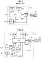
- a single-chip system 10 of this typeconventionally comprises a central processing unit (CPU) 11 , a read-only memory (ROM) 12 , a random-access memory (RAM) 13 , a serial input-output interface (SIO) 14 , a clock divider (DIV) 15 , and various on-chip peripheral circuits (not shown).
- CPUcentral processing unit
- ROMread-only memory
- RAMrandom-access memory
- SIOserial input-output interface
- DIVclock divider
- the CPU 11carries out prescribed computations and control processing according to a program stored in the chip's memory (the ROM 12 and/or RAM 13 ).
- the ROM 12is a nonvolatile memory that retains its data even after power is switched off.
- Programs stored in the ROM 12include a bootstrap program or initial program loader (IPL), interrupt handlers that handle external interrupts, and other programs.
- the RAM 13is a volatile memory that loses its data when power is switched off. The RAM 13 is used to store application programs and data being processed.
- the serial input-output interface 14is used to transfer data between the CPU 11 and an external device (in this case, an external memory device 30 such as a flash memory).
- the serial input-output interface 14converts parallel data received from the CPU 11 to serial data and sends the data to the external device, and converts serial data received from the external device to parallel data and supplies the data to the CPU 11 .
- the clock divider 15divides the frequency (for example, 10 MHz) of a system clock SCK received from an external source to obtain a high-speed clock signal CKH (with a frequency of, for example, 5 MHz), which is supplied to the CPU 11 , and a low-speed clock signal CKL (with a frequency of, for example, 1 MHz), which is supplied to the serial input-output interface 14 and used for serial data transfer.
- CKHwith a frequency of, for example, 5 MHz
- CKLwith a frequency of, for example, 1 MHz
- the CPU 11When the CPU 11 has finished executing a series of processes and is ready to power down into the power-saving mode, the CPU 11 reads out the data stored in the RAM 13 and supplies the data one byte at a time to the serial input-output interface 14 .
- the serial input-output interface 14converts the data received from the CPU 11 to serial data synchronized with the low-speed clock signal CKL and transfers the data to the external memory device 30 .
- the serial input-output interface 14sends a transfer completion signal DON to the CPU 11 .
- the CPU 11then supplies the next byte of data to the serial input-output interface 14 .
- the CPU 11When all the, necessary data have been transferred to the external memory device 30 , the CPU 11 powers off prescribed circuits, including the RAM 13 , and goes into the power-saving mode. Even in this power-saving mode, the CPU 11 , ROM 12 , and clock divider 15 remain powered so that they can detect an external interrupt INT and execute a transition from the power-saving mode to the normal mode.
- the CPU 11Upon detection of an external interrupt INT in the power-saving mode, the CPU 11 powers up the circuits that were powered off, operating according to a program stored in the ROM 12 . The CPU 11 then sends a byte data read command to the serial input-output interface 14 . The serial input-output interface 14 retrieves one byte of data from the external memory device 30 in response to the instruction, and sends a transfer completion signal DON to the CPU 11 . The CPU 11 stores the retrieved data in the RAM 13 . The CPU 11 continues to issue data read commands to the serial input-output interface 14 until all necessary data have been stored in the RAM 13 . When the necessary data have been stored in the RAM 13 , the CPU 11 resumes normal operation.
- a microelectronic system in which a uniform transmission speed is maintained between the microelectronic system and peripheral units even when the clock frequency is changed to conserve poweris described in Japanese Patent Application Publication No. 8-234865.
- a problem with the integrated circuit described aboveis that during the transitions between the normal mode and the power-saving mode, while data are being transferred between the serial input-output interface 14 and the external memory device 30 in synchronization with the low-speed clock signal CKL supplied to the serial input-output interface 14 , the CPU 11 continues to receive the high-speed clock signal CKH. The CPU 11 therefore operates on a clock signal with a higher speed than necessary, consuming power needlessly.
- the CPU 11has to wait for an external interrupt INT and carry out a transition from the power-saving mode to the normal mode, so the high-speed clock signal CKH cannot be halted, limiting the reduction of power consumption.
- An object of the present inventionis to conserve power during transitions of an integrated circuit between its normal operating mode and a power-saving mode, while data are being transferred between a volatile memory in the integrated circuit and an external memory device.
- the invented integrated circuitthus includes a central processing unit and a volatile memory and is connected to an external memory device.
- the central processing unitoperates on a first clock signal and executes logic processing while the volatile memory stores data.
- the central processing unithalts and the volatile memory loses its stored data.
- the central processing unitsaves data from the volatile memory to the external memory device.
- the central processing unitrestores the data from the external memory device to the volatile memory.
- the integrated circuitalso includes a data input-output circuit that the central processing unit uses to transfer data between the volatile memory and the external memory device, and a clock divider.
- the clock dividerdivides the frequency of the first clock signal to obtain a second clock signal and supplies the second clock signal to the data input-output circuit as a data transfer clock signal.
- the integrated circuitalso includes an interrupt detector, a selector, and a clock supply circuit.
- the interrupt detectordetects an external interrupt.
- the selectorselects the second clock signal in the power-saving mode and during the transitions between the power-saving mode and the normal mode, and selects the first clock signal in the normal mode.
- the clock supply circuitsupplies the clock signal selected by the first selector to the central processing unit in the normal mode and during the transitional periods, and halts the clock supply in the power-saving mode.
- the clock supply circuitsupplies the second clock signal to the central processing unit until it finishes saving data from the volatile memory to the external memory unit.
- the clock supply circuitthen halts the clock supply to the central processing unit until the interrupt detector detects the external interrupt, at which point the clock supply circuit resumes supply of the second clock signal while the central processing unit restores data from the external memory device to the volatile memory.
- the first selectorselects the first clock again and the central processing unit resumes normal operation.
- the central processing unitoperates on the second clock signal, conserving power because the second clock signal has a lower frequency than the first clock signal.
- the lower frequencyis adequate because during the transitional periods the central processing unit only has to keep pace with the data input-output circuit, which always operates on the second clock signal.
- FIG. 1is a block diagram of a conventional integrated circuit
- FIG. 2is a block diagram of an integrated circuit illustrating a first embodiment of the invention
- FIG. 3is a signal waveform diagram illustrating the operation of the integrated circuit in FIG. 2 ;
- FIG. 4is a flowchart illustrating the operation of the integrated circuit in FIG. 2 during a transition from the normal mode to the power-saving mode;
- FIG. 5is a flowchart illustrating the operation of the integrated circuit in FIG. 2 during a transition from the power-saving mode to the normal mode
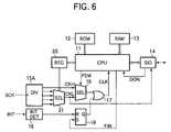
- FIG. 6is a block diagram of an integrated circuit illustrating a second embodiment of the invention.
- the integrated circuit 10 in the first embodimenthas a CPU 11 , ROM 12 , RAM 13 , serial input-output interface 14 , and clock divider 15 .
- the CPU 11carries out prescribed computation and control processing according to a program stored in the ROM 12 or RAM 13 in synchronization with a clock signal CLK.
- the ROM 12stores a bootstrap program or IPL, interrupt handlers that handle external interrupts, and other programs, while the RAM 13 is used to store application programs and data being processed.
- the serial input-output interface 14carries out data transfers between the CPU 11 and the external memory device 30 (in this case, a flash memory or the like).
- the serial input-output interface 14converts the parallel data received from the CPU 11 to serial data and supplies the data to the CPU 11 .
- the serial input-output interface 14sends a transfer completion signal DON to the CPU 11 upon completion of one byte of data transfer.
- the clock divider 15divides the frequency of the system clock SCK (for example, 10 MHz) received from an external source to obtain a high-speed clock signal CKH (with a frequency of for example 5 MHz) and further divides the frequency of the high-speed clock signal CKH to obtain a low-speed clock signal CKL (with a frequency of, for example, 1 MHz).
- the low-speed clock signal CKLis supplied to the serial input-output interface 14 as a timing signal for serial data transfer.
- the integrated circuit 10further comprises a selector (SEL) 16 , a logical OR gate 17 , an interrupt detector (INT DET) 18 , a set/reset type flip-flop 19 , and various peripheral circuits (not shown).
- SELselector
- INT DETinterrupt detector
- the selector 16selects one of the two clock signals CKL and CKH generated by the clock divider 15 , in response to a mode select signal PSM received from the CPU 11 .
- the output terminal of the selector 16is connected to one of the input terminals of the logical OR gate 17 .
- the interrupt detector 18is used to detect an external interrupt INT.
- the output terminal of the interrupt detector 18is connected to the reset terminal R of the flip-flop 19 .
- the set terminal S of the flip-flop 19receives a completion signal FIN from the CPU 11 , and the output terminal of the 19 is connected to the other input terminal of the logical OR gate 17 .
- the output signal of the logical OR gate 17is supplied to the CPU 11 as its clock signal (CLK).
- CLKclock signal
- the logical OR gate 17 and flip-flop 19constitute the clock supply circuit for the CPU 11 .
- the flip-flop 19In normal operation, the flip-flop 19 is reset, and the signal S 19 output from the flip-flop 19 is at the low logic level (L in FIG. 3 ).
- the mode select signal PSM supplied to the selector 16 from the CPU 11is set (to the high logic level, H in FIG. 3 , for example) to select the normal operation mode, and the high-speed clock signal CKH generated by the clock divider 15 is selected and supplied to the logical OR gate 17 .
- the 5-MHz clock signal CKHis supplied to the CPU 11 as its clock signal CLK.
- the 1-MHz clock signal CKLis supplied to the serial input-output interface 14 as the data transfer clock signal.
- the CPU 11When the CPU 11 has finished executing a series of processes and is ready to power down into the power-saving mode (step 41 in FIG. 4 ), the CPU 11 switches the mode select signal PSM (to the low logic level, for example) to select the power-saving mode (step 42 ).
- the low-speed clock signal CKLis selected by the selector 16 and supplied to the CPU 11 through the logical OR gate 17 as the clock signal CKL (step 43 ).
- the frequency of the clock signal CLK supplied to the CPU 11is reduced from 5 MHz to 1 MHz, as shown in FIG. 3 .
- the CPU 11Reads one byte of the data stored in the RAM 13 (step 44 ), supplies the data to the serial input-output interface 14 (step 45 ), and gives a serial transfer command (step 46 ). Also operating on the 1-MHz clock signal, the serial input-output interface 14 converts the data received from the CPU 11 to serial data and transfers the data to the external memory device 30 (step 47 ). When the transfer of one byte of data is completed, the serial input-output interface 14 sends a completion signal DON to the CPU 11 (step 48 ). The CPU 11 then supplies the next byte of data to the serial input-output interface 14 (step 44 ).
- the circuits that have been powered offstop operating and lose their stored information.
- the flip-flop 19is set by the completion signal FIN, the S 19 signal goes high, and the clock signal CLK output from the logical OR gate 17 is held fixed at the high level, as shown in FIG. 3 .
- the CPU 11then stops operating, but as its power is not switched off, the CPU 11 remains in the state it was in just before it stopped operating.
- the mode select signal PSM output from the CPU 11therefore remains low. Meanwhile, the interrupt detector 18 is kept constantly powered to await the input of an external interrupt INT.
- the interrupt detector 18Upon detection of an external interrupt INT in the power-saving mode (step 61 in FIG. 61 ), the interrupt detector 18 resets the flip-flop 19 . The signal S 19 then goes low, and the clock signal CKL selected by the selector 16 is supplied to the CPU 11 as its clock signal CLK (step 62 ).
- the CPU 11resumes operation from the state it was in before it stopped operating, and provides power to the circuits, such as the RAM 13 , that were powered off to reduce power consumption.
- the integrated circuit 10 in the first embodimenthas a selector 16 that switches the clock signal CLK supplied to the CPU 11 to the low-speed clock signal CKL during the transitions between the power-saving mode and the normal mode. Power consumption by the CPU 11 is thereby reduced during the transfer of data between the RAM 13 and the external memory device 30 .
- the integrated circuit 10also has a logical OR gate 17 that halts the clock signal CLK supplied to the CPU 11 in the power-saving mode.
- the CPU 11therefore stops operating in the power-saving mode, and the power consumption of the CPU 11 is further reduced.
- the data transfer carried out between the integrated circuit 10 and the external memory device 30is a serial transfer, but the invention can also be practiced with an external memory device that carries out parallel data transfer. In that case, a parallel input-output circuit should be used in place of the serial input-output interface 14 .
- the clock divider 15divides the frequency of the system clock SCK by two to generate the high-speed clock signal CKH, and by ten to generate the low-speed clock signal CKL, but the invention can be practiced with other frequency division ratios. For example, it is possible to use the system clock SCK directly as the high-speed clock signal CKH without dividing the frequency.
- the second embodimentadds a register (REG) 20 and a second selector 21 to the integrated circuit in the first embodiment, and uses a different clock divider 15 A, which divides the frequency of the system clock SCK to generate a plurality of low-speed divided clock signals, as well as the high-speed clock signal CKH.
- REGregister
- CKHhigh-speed clock signal
- Selector 21selects one of the plurality of low-speed divided clock signals generated by the clock divider 15 A according to the value set in the register 20 and outputs the selected clock signal as the low-speed clock signal CKL.
- the value in the register 20is set by the CPU 11 .
- the high-speed clock signal CKH generated by the clock divider 15 A and the low-speed clock signal CKL selected by selector 21are supplied to selector 16 , which selects one of the two clock signals according to the mode select signal PSM received from the CPU 11 .
- the second embodimenthas the same configurations as the first embodiment illustrated in FIG. 2 .
- the integrated circuit in FIG. 6operates in the same way as the integrated circuit in FIG. 2 , with the exception that the low-speed clock signal CKL is selected according to the value set in the register 20 .
- the integrated circuit in the second embodimenthas a first selector 16 that switches the clock signal CLK supplied to the CPU 11 to a low-speed clock signal CKL during the transitions between the power-saving mode and the normal mode, and a logical OR gate 17 that halts the clock signal CLK supplied to the CPU 11 in the power-saving mode. Therefore, the second embodiment provides the same advantages as the first embodiment.
- the integrated circuit in the second embodimenthas a register 20 and a second selector 21 for selecting the low-speed clock signal CKL. This offers the advantage that the optimal frequency of the data transfer clock signal CKL can be selected according to the data transfer rate of the external memory device.
- the integrated circuit in FIG. 6is configured to have the CPU 11 set a value in the register 20 , but it is also possible to have the value set by the external memory device, using signals from a connector connecting the serial input-output interface 14 and the external memory device, or to replace the register 20 with an external switch.
Landscapes
- Engineering & Computer Science (AREA)
- Theoretical Computer Science (AREA)
- Physics & Mathematics (AREA)
- General Engineering & Computer Science (AREA)
- General Physics & Mathematics (AREA)
- Microcomputers (AREA)
- Power Sources (AREA)
- Memory System (AREA)
Abstract
Description
Claims (11)
Applications Claiming Priority (2)
| Application Number | Priority Date | Filing Date | Title |
|---|---|---|---|
| JP2005143855AJP4724461B2 (en) | 2005-05-17 | 2005-05-17 | System LSI |
| JP2005-143855 | 2005-05-17 |
Publications (2)
| Publication Number | Publication Date |
|---|---|
| US20060282694A1 US20060282694A1 (en) | 2006-12-14 |
| US7600142B2true US7600142B2 (en) | 2009-10-06 |
Family
ID=37425206
Family Applications (1)
| Application Number | Title | Priority Date | Filing Date |
|---|---|---|---|
| US11/408,089Active2027-11-23US7600142B2 (en) | 2005-05-17 | 2006-04-21 | Integrated circuit conserving power during transitions between normal and power-saving modes |
Country Status (4)
| Country | Link |
|---|---|
| US (1) | US7600142B2 (en) |
| JP (1) | JP4724461B2 (en) |
| KR (1) | KR101262740B1 (en) |
| CN (1) | CN100530045C (en) |
Cited By (11)
| Publication number | Priority date | Publication date | Assignee | Title |
|---|---|---|---|---|
| US20100169698A1 (en)* | 2008-12-25 | 2010-07-01 | Kabushiki Kaisha Toshiba | Recording medium control element, recording medium control circuit board, and recording medium control device |
| US8874831B2 (en) | 2007-06-01 | 2014-10-28 | Netlist, Inc. | Flash-DRAM hybrid memory module |
| US8880791B2 (en) | 2007-06-01 | 2014-11-04 | Netlist, Inc. | Isolation switching for backup of registered memory |
| US8904098B2 (en) | 2007-06-01 | 2014-12-02 | Netlist, Inc. | Redundant backup using non-volatile memory |
| US8990489B2 (en) | 2004-01-05 | 2015-03-24 | Smart Modular Technologies, Inc. | Multi-rank memory module that emulates a memory module having a different number of ranks |
| US9436600B2 (en) | 2013-06-11 | 2016-09-06 | Svic No. 28 New Technology Business Investment L.L.P. | Non-volatile memory storage for multi-channel memory system |
| US10198350B2 (en) | 2011-07-28 | 2019-02-05 | Netlist, Inc. | Memory module having volatile and non-volatile memory subsystems and method of operation |
| US10248328B2 (en) | 2013-11-07 | 2019-04-02 | Netlist, Inc. | Direct data move between DRAM and storage on a memory module |
| US10372551B2 (en) | 2013-03-15 | 2019-08-06 | Netlist, Inc. | Hybrid memory system with configurable error thresholds and failure analysis capability |
| US10380022B2 (en) | 2011-07-28 | 2019-08-13 | Netlist, Inc. | Hybrid memory module and system and method of operating the same |
| US10838646B2 (en) | 2011-07-28 | 2020-11-17 | Netlist, Inc. | Method and apparatus for presearching stored data |
Families Citing this family (10)
| Publication number | Priority date | Publication date | Assignee | Title |
|---|---|---|---|---|
| CN1893477B (en)* | 2005-07-04 | 2010-06-09 | 深圳市东进通讯技术股份有限公司 | SCX card and CTI system adopting same |
| US7886122B2 (en)* | 2006-08-22 | 2011-02-08 | Qimonda North America Corp. | Method and circuit for transmitting a memory clock signal |
| CN101657798A (en) | 2007-04-11 | 2010-02-24 | 松下电器产业株式会社 | Data saving system, data returning system, data saving method and data returning method |
| TW200849087A (en)* | 2007-06-01 | 2008-12-16 | Holtek Semiconductor Inc | Method of accelerating the excution of repeatative commands and its micro controller |
| JP2009124508A (en)* | 2007-11-15 | 2009-06-04 | Sony Corp | Information storage device, information display method, and computer program |
| JP5305076B2 (en)* | 2008-09-03 | 2013-10-02 | 株式会社デンソー | Microcomputer |
| US8347132B2 (en)* | 2009-01-07 | 2013-01-01 | Taiwan Semiconductor Manufacturing Company, Ltd. | System and method for reducing processor power consumption |
| JP5423207B2 (en)* | 2009-07-24 | 2014-02-19 | アイシン精機株式会社 | Opening and closing body control device for vehicle |
| KR101636324B1 (en)* | 2009-08-19 | 2016-07-05 | 삼성전자주식회사 | Power gating device |
| US10303235B2 (en)* | 2015-03-04 | 2019-05-28 | Qualcomm Incorporated | Systems and methods for implementing power collapse in a memory |
Citations (3)
| Publication number | Priority date | Publication date | Assignee | Title |
|---|---|---|---|---|
| JPH08234865A (en) | 1995-02-24 | 1996-09-13 | Canon Inc | Equipment with a microcomputer |
| US20040148533A1 (en)* | 2003-01-28 | 2004-07-29 | Ken Nicholas | Power management controller and method |
| US7225353B1 (en)* | 2001-10-03 | 2007-05-29 | Palm, Inc. | Information preservation on a portable electronic device |
Family Cites Families (2)
| Publication number | Priority date | Publication date | Assignee | Title |
|---|---|---|---|---|
| JPH1115572A (en)* | 1997-06-23 | 1999-01-22 | Diamond Electric Mfg Co Ltd | Power interruption back-up circuit |
| KR20020026814A (en)* | 2000-10-02 | 2002-04-12 | 포만 제프리 엘 | Method and Apparatus for Suspending And Resuming Operation of A Computer System |
- 2005
- 2005-05-17JPJP2005143855Apatent/JP4724461B2/ennot_activeExpired - Lifetime
- 2006
- 2006-01-24KRKR1020060007293Apatent/KR101262740B1/ennot_activeExpired - Fee Related
- 2006-01-28CNCNB2006100820576Apatent/CN100530045C/enactiveActive
- 2006-04-21USUS11/408,089patent/US7600142B2/enactiveActive
Patent Citations (4)
| Publication number | Priority date | Publication date | Assignee | Title |
|---|---|---|---|---|
| JPH08234865A (en) | 1995-02-24 | 1996-09-13 | Canon Inc | Equipment with a microcomputer |
| US5751172A (en)* | 1995-02-24 | 1998-05-12 | Canon Kabushiki Kaisha | Electronic apparatus having a computer |
| US7225353B1 (en)* | 2001-10-03 | 2007-05-29 | Palm, Inc. | Information preservation on a portable electronic device |
| US20040148533A1 (en)* | 2003-01-28 | 2004-07-29 | Ken Nicholas | Power management controller and method |
Cited By (25)
| Publication number | Priority date | Publication date | Assignee | Title |
|---|---|---|---|---|
| US8990489B2 (en) | 2004-01-05 | 2015-03-24 | Smart Modular Technologies, Inc. | Multi-rank memory module that emulates a memory module having a different number of ranks |
| US10755757B2 (en) | 2004-01-05 | 2020-08-25 | Smart Modular Technologies, Inc. | Multi-rank memory module that emulates a memory module having a different number of ranks |
| US20150242313A1 (en)* | 2007-06-01 | 2015-08-27 | Netlist, Inc. | Flash-dram hybrid memory module |
| US9921762B2 (en) | 2007-06-01 | 2018-03-20 | Netlist, Inc. | Redundant backup using non-volatile memory |
| US8904099B2 (en) | 2007-06-01 | 2014-12-02 | Netlist, Inc. | Isolation switching for backup memory |
| US8880791B2 (en) | 2007-06-01 | 2014-11-04 | Netlist, Inc. | Isolation switching for backup of registered memory |
| US11232054B2 (en) | 2007-06-01 | 2022-01-25 | Netlist, Inc. | Flash-dram hybrid memory module |
| US9158684B2 (en)* | 2007-06-01 | 2015-10-13 | Netlist, Inc. | Flash-DRAM hybrid memory module |
| US9269437B2 (en) | 2007-06-01 | 2016-02-23 | Netlist, Inc. | Isolation switching for backup memory |
| US11016918B2 (en) | 2007-06-01 | 2021-05-25 | Netlist, Inc. | Flash-DRAM hybrid memory module |
| US8874831B2 (en) | 2007-06-01 | 2014-10-28 | Netlist, Inc. | Flash-DRAM hybrid memory module |
| US9928186B2 (en) | 2007-06-01 | 2018-03-27 | Netlist, Inc. | Flash-DRAM hybrid memory module |
| US8904098B2 (en) | 2007-06-01 | 2014-12-02 | Netlist, Inc. | Redundant backup using non-volatile memory |
| US20100169698A1 (en)* | 2008-12-25 | 2010-07-01 | Kabushiki Kaisha Toshiba | Recording medium control element, recording medium control circuit board, and recording medium control device |
| US10380022B2 (en) | 2011-07-28 | 2019-08-13 | Netlist, Inc. | Hybrid memory module and system and method of operating the same |
| US10198350B2 (en) | 2011-07-28 | 2019-02-05 | Netlist, Inc. | Memory module having volatile and non-volatile memory subsystems and method of operation |
| US10838646B2 (en) | 2011-07-28 | 2020-11-17 | Netlist, Inc. | Method and apparatus for presearching stored data |
| US11561715B2 (en) | 2011-07-28 | 2023-01-24 | Netlist, Inc. | Method and apparatus for presearching stored data |
| US10372551B2 (en) | 2013-03-15 | 2019-08-06 | Netlist, Inc. | Hybrid memory system with configurable error thresholds and failure analysis capability |
| US11200120B2 (en) | 2013-03-15 | 2021-12-14 | Netlist, Inc. | Hybrid memory system with configurable error thresholds and failure analysis capability |
| US9996284B2 (en) | 2013-06-11 | 2018-06-12 | Netlist, Inc. | Non-volatile memory storage for multi-channel memory system |
| US9436600B2 (en) | 2013-06-11 | 2016-09-06 | Svic No. 28 New Technology Business Investment L.L.P. | Non-volatile memory storage for multi-channel memory system |
| US10719246B2 (en) | 2013-06-11 | 2020-07-21 | Netlist, Inc. | Non-volatile memory storage for multi-channel memory system |
| US11314422B2 (en) | 2013-06-11 | 2022-04-26 | Netlist, Inc. | Non-volatile memory storage for multi-channel memory system |
| US10248328B2 (en) | 2013-11-07 | 2019-04-02 | Netlist, Inc. | Direct data move between DRAM and storage on a memory module |
Also Published As
| Publication number | Publication date |
|---|---|
| KR101262740B1 (en) | 2013-05-09 |
| JP4724461B2 (en) | 2011-07-13 |
| KR20060119728A (en) | 2006-11-24 |
| CN1866166A (en) | 2006-11-22 |
| CN100530045C (en) | 2009-08-19 |
| JP2006323469A (en) | 2006-11-30 |
| US20060282694A1 (en) | 2006-12-14 |
Similar Documents
| Publication | Publication Date | Title |
|---|---|---|
| US7600142B2 (en) | Integrated circuit conserving power during transitions between normal and power-saving modes | |
| US6895530B2 (en) | Method and apparatus for controlling a data processing system during debug | |
| JP4822472B2 (en) | Data processing system | |
| US6397338B2 (en) | Power management circuit that qualifies powergood disposal signal | |
| JP4515093B2 (en) | CPU power-down method and apparatus therefor | |
| CN100354793C (en) | Integrated circuit device | |
| US7941683B2 (en) | Data processing device with low-power cache access mode | |
| EP2290527B1 (en) | Microprocessor with automatic selection of SIMD parallelism | |
| KR100806284B1 (en) | High Energy Efficiency Processor Using Dynamic Voltage Scaling | |
| US6694442B2 (en) | Method for saving power in a computer by idling system controller and reducing frequency of host clock signal used by system controller | |
| JP3475510B2 (en) | Integrated circuit with power saving function | |
| JP3552213B2 (en) | SD memory card host controller and clock control method | |
| US7219248B2 (en) | Semiconductor integrated circuit operable to control power supply voltage | |
| US5872903A (en) | Integrated circuit device with a memory that preserves its content independently of a synchronizing signal when given a self-control request | |
| US20050060593A1 (en) | Inquiring apparatus and method thereof | |
| CN110286741B (en) | Solid state disk system-on-chip power consumption management method and device | |
| KR101236393B1 (en) | Electric device and control method thereof | |
| JPH11328011A (en) | Storage controller and information processor | |
| JPH07191954A (en) | Microcomputer system | |
| JPH04195316A (en) | power saving circuit | |
| JPH1069460A (en) | Bus control device | |
| JPH03242717A (en) | Microprocessor |
Legal Events
| Date | Code | Title | Description |
|---|---|---|---|
| AS | Assignment | Owner name:OKI ELECTRIC INDUSTRY CO., LTD., JAPAN Free format text:ASSIGNMENT OF ASSIGNORS INTEREST;ASSIGNOR:ICHIKAWA, TAKESHI;REEL/FRAME:017812/0956 Effective date:20060314 | |
| AS | Assignment | Owner name:OKI SEMICONDUCTOR CO., LTD., JAPAN Free format text:CHANGE OF NAME;ASSIGNOR:OKI ELECTRIC INDUSTRY CO., LTD.;REEL/FRAME:022162/0586 Effective date:20081001 Owner name:OKI SEMICONDUCTOR CO., LTD.,JAPAN Free format text:CHANGE OF NAME;ASSIGNOR:OKI ELECTRIC INDUSTRY CO., LTD.;REEL/FRAME:022162/0586 Effective date:20081001 | |
| STCF | Information on status: patent grant | Free format text:PATENTED CASE | |
| CC | Certificate of correction | ||
| FPAY | Fee payment | Year of fee payment:4 | |
| AS | Assignment | Owner name:LAPIS SEMICONDUCTOR CO., LTD., JAPAN Free format text:CHANGE OF NAME;ASSIGNOR:OKI SEMICONDUCTOR CO., LTD;REEL/FRAME:032495/0483 Effective date:20111003 | |
| FPAY | Fee payment | Year of fee payment:8 | |
| MAFP | Maintenance fee payment | Free format text:PAYMENT OF MAINTENANCE FEE, 12TH YEAR, LARGE ENTITY (ORIGINAL EVENT CODE: M1553); ENTITY STATUS OF PATENT OWNER: LARGE ENTITY Year of fee payment:12 |