US7598788B2 - Current-controlled CMOS (C3MOS) fully differential integrated delay cell with variable delay and high bandwidth - Google Patents
Current-controlled CMOS (C3MOS) fully differential integrated delay cell with variable delay and high bandwidthDownload PDFInfo
- Publication number
- US7598788B2 US7598788B2US11/320,401US32040105AUS7598788B2US 7598788 B2US7598788 B2US 7598788B2US 32040105 AUS32040105 AUS 32040105AUS 7598788 B2US7598788 B2US 7598788B2
- Authority
- US
- United States
- Prior art keywords
- differential
- transistor
- differential transistor
- current source
- drain
- Prior art date
- Legal status (The legal status is an assumption and is not a legal conclusion. Google has not performed a legal analysis and makes no representation as to the accuracy of the status listed.)
- Expired - Fee Related
Links
- 239000003990capacitorSubstances0.000claimsdescription12
- 230000004044responseEffects0.000claimsdescription10
- 239000004065semiconductorSubstances0.000claimsdescription8
- 229910044991metal oxideInorganic materials0.000claimsdescription6
- 150000004706metal oxidesChemical class0.000claimsdescription6
- 239000000872bufferSubstances0.000abstractdescription32
- 230000001965increasing effectEffects0.000abstractdescription6
- 238000013461designMethods0.000abstractdescription5
- 238000000034methodMethods0.000description16
- 238000004891communicationMethods0.000description13
- 238000013459approachMethods0.000description7
- 230000008569processEffects0.000description7
- 238000005516engineering processMethods0.000description5
- 230000001939inductive effectEffects0.000description4
- 230000008439repair processEffects0.000description3
- VYPSYNLAJGMNEJ-UHFFFAOYSA-NSilicium dioxideChemical compoundO=[Si]=OVYPSYNLAJGMNEJ-UHFFFAOYSA-N0.000description2
- XUIMIQQOPSSXEZ-UHFFFAOYSA-NSiliconChemical compound[Si]XUIMIQQOPSSXEZ-UHFFFAOYSA-N0.000description2
- 230000015556catabolic processEffects0.000description2
- 230000000295complement effectEffects0.000description2
- 238000006731degradation reactionMethods0.000description2
- 230000005669field effectEffects0.000description2
- 238000001914filtrationMethods0.000description2
- 238000012986modificationMethods0.000description2
- 230000004048modificationEffects0.000description2
- 230000001172regenerating effectEffects0.000description2
- 229910052710siliconInorganic materials0.000description2
- 239000010703siliconSubstances0.000description2
- 230000003068static effectEffects0.000description2
- 238000004458analytical methodMethods0.000description1
- 230000005540biological transmissionEffects0.000description1
- 230000000593degrading effectEffects0.000description1
- 230000001934delayEffects0.000description1
- 238000011161developmentMethods0.000description1
- 230000000694effectsEffects0.000description1
- 238000010348incorporationMethods0.000description1
- 239000011810insulating materialSubstances0.000description1
- 238000004519manufacturing processMethods0.000description1
- 239000000463materialSubstances0.000description1
- 230000007246mechanismEffects0.000description1
- 230000003071parasitic effectEffects0.000description1
- 229910021420polycrystalline siliconInorganic materials0.000description1
- 229920005591polysiliconPolymers0.000description1
- 235000012239silicon dioxideNutrition0.000description1
- 239000000377silicon dioxideSubstances0.000description1
- 239000000758substrateSubstances0.000description1
- 238000012546transferMethods0.000description1
Images


Classifications
- H—ELECTRICITY
- H03—ELECTRONIC CIRCUITRY
- H03K—PULSE TECHNIQUE
- H03K5/00—Manipulating of pulses not covered by one of the other main groups of this subclass
- H03K5/13—Arrangements having a single output and transforming input signals into pulses delivered at desired time intervals
- H03K5/133—Arrangements having a single output and transforming input signals into pulses delivered at desired time intervals using a chain of active delay devices
- H—ELECTRICITY
- H03—ELECTRONIC CIRCUITRY
- H03K—PULSE TECHNIQUE
- H03K3/00—Circuits for generating electric pulses; Monostable, bistable or multistable circuits
- H03K3/02—Generators characterised by the type of circuit or by the means used for producing pulses
- H03K3/353—Generators characterised by the type of circuit or by the means used for producing pulses by the use, as active elements, of field-effect transistors with internal or external positive feedback
- H03K3/356—Bistable circuits
- H03K3/356017—Bistable circuits using additional transistors in the input circuit
- H03K3/356034—Bistable circuits using additional transistors in the input circuit the input circuit having a differential configuration
- H—ELECTRICITY
- H03—ELECTRONIC CIRCUITRY
- H03K—PULSE TECHNIQUE
- H03K5/00—Manipulating of pulses not covered by one of the other main groups of this subclass
- H03K5/01—Shaping pulses
- H03K5/04—Shaping pulses by increasing duration; by decreasing duration
- H03K5/07—Shaping pulses by increasing duration; by decreasing duration by the use of resonant circuits
- H—ELECTRICITY
- H03—ELECTRONIC CIRCUITRY
- H03K—PULSE TECHNIQUE
- H03K5/00—Manipulating of pulses not covered by one of the other main groups of this subclass
- H03K5/13—Arrangements having a single output and transforming input signals into pulses delivered at desired time intervals
- H03K5/145—Arrangements having a single output and transforming input signals into pulses delivered at desired time intervals by the use of resonant circuits
- H—ELECTRICITY
- H03—ELECTRONIC CIRCUITRY
- H03K—PULSE TECHNIQUE
- H03K5/00—Manipulating of pulses not covered by one of the other main groups of this subclass
- H03K2005/00013—Delay, i.e. output pulse is delayed after input pulse and pulse length of output pulse is dependent on pulse length of input pulse
- H03K2005/00019—Variable delay
- H03K2005/00026—Variable delay controlled by an analog electrical signal, e.g. obtained after conversion by a D/A converter
- H—ELECTRICITY
- H03—ELECTRONIC CIRCUITRY
- H03K—PULSE TECHNIQUE
- H03K5/00—Manipulating of pulses not covered by one of the other main groups of this subclass
- H03K2005/00013—Delay, i.e. output pulse is delayed after input pulse and pulse length of output pulse is dependent on pulse length of input pulse
- H03K2005/0015—Layout of the delay element
- H03K2005/00195—Layout of the delay element using FET's
- H03K2005/00208—Layout of the delay element using FET's using differential stages
Definitions
- the inventionrelates generally to the field of communication devices; and, more particularly, it relates to the field of delay cells that can be implemented within such communication devices.
- DLLdelay locked loop
- FIG. 1illustrates an embodiment of a current-controlled CMOS (C3MOS) wideband data amplifier circuit.
- C3MOSCMOS
- FIG. 2illustrates an embodiment of a variable delay cell.
- FIG. 3illustrates another embodiment of a variable delay cell.
- FIG. 4illustrates an embodiment of a two-path adjustable high bandwidth delay cell.
- FIG. 5illustrates an embodiment of a wideband variable delay cell.
- FIG. 6illustrates an embodiment of delay through a cross-coupled differential pair (normalized) in response to current in a buffer stage (normalized).
- CMOS process technologyrefers generally to a variety of well established CMOS fabrication processes that form a field-effect transistor over a silicon substrate with a gate terminal typically made of polysilicon material disposed on top of an insulating material such as silicon dioxide.
- CMOS logicrefers to the use of complementary CMOS transistors (n-channel and p-channel, implemented using NMOS (Negative-Channel Metal-Oxide Semiconductor) transistors or PMOS (Positive-Channel Metal-Oxide Semiconductor) transistors) to form various logic gates and more complex logic circuitry, wherein zero static current is dissipated.
- CMOScomplementary metal-oxide-semiconductor field-effect transistor
- shunt peakingis one approach that has resulted in improved gain-bandwidth product.
- Shunt peakinginvolves putting an inductor in series with the output resistor to expand the bandwidth of the circuit.
- inductive broadbanding technique combined with C3MOS circuitryis described in greater detail in commonly-assigned U.S. patent application Ser. No. 09/610,905, now U.S. Pat. No. 6,340,899 B1, entitled “Current-Controlled CMOS Circuits with Inductive Broadbanding,” by M. Green, which is hereby incorporated by reference in its entirety for all purposes as indicated above.
- FIG. 1illustrates an embodiment 100 of a current-controlled CMOS (C3MOS) wideband data amplifier circuit.
- a current source transistorcan be biased by a bias voltage so that a constant current flows from drain to source in the current source transistor.
- Two separate differential transistorscompose a wideband differential transistor pair.
- a first differential transistorhas its gate tied to the negative end of a first series peaking inductor L 1 , while a positive differential input signal INP is coupled to the positive end of the first series peaking inductor L 1 .
- a second differential transistorhas its gate tied to the negative end of a second series peaking inductor L 2 , while a negative differential input signal INN is coupled to the positive end of the second series peaking inductor L 2 .
- a first output resistor R 3has its negative end tied to the drain of the first differential transistor, and has its positive end tied to the negative end of a first shunt peaking inductor L 3 .
- a second output resistor R 4has its negative end tied to the drain of the second differential transistor, and has its positive end tied to the negative end of a second shunt peaking inductor L 4 .
- the positive ends of the first and second shunt peaking inductors L 3 and L 4are tied to the positive supply voltage (shown as V CC ).
- the first and second output resistors R 3 and R 4have the same resistance value R, and the first and second shunt peaking inductors L 3 and L 4 have the same inductances.
- a first capacitor C 1(which may be referred to as a first Miller cancellation capacitor C 1 ) has its positive end coupled to the drain of the second differential transistor, and has its negative end coupled to the gate of the first differential transistor.
- a second capacitor C 2(which may be referred to as a second Miller cancellation capacitor C 2 ) has its positive end coupled to the drain of the first differential transistor, and has its negative end coupled to the gate of the second differential transistor.
- a first output signal OUTPis taken at the drain of the second differential transistor, and the second output signal OUTN is taken at the drain of the first differential transistor.
- Input series inductors (L 1 and L 2 )resonate with the capacitance at the input of the differential pair at high frequencies and thus extend the bandwidth of the amplifier.
- the inductors (L 1 and L 2 )act as high impedance chokes between the termination resistors (shown as two series connected 50 ⁇ resistors) and the capacitors and thus also improve the input reflection for the C3MOS wideband data amplifier circuit of this embodiment 100 .
- FIG. 2illustrates an embodiment 200 of a variable delay cell.
- This embodiment 200shows a basic building block of a data synchronization circuit.
- the input data (DIN)is retimed by a flip-flop (FF) driven by a clock signal (CLK).
- CLKclock signal
- a delay cellis often inserted between the input data (DIN) and the FF so that the timing relation between the clock (CLK) and data (DIN) at the input of the FF can be adjusted to compensate for any phase variations of the input signals or circuit delay variations due to changes in process, voltage supply or temperature (PVT).
- the delay cellneeds to have continuously higher and higher bandwidth in order to preserve the signal integrity of the input data.
- FIG. 3illustrates another embodiment 300 of a variable delay cell.
- This embodiment 300is another example by which a variable delay cell can be employed.
- the embodiment 300is a 5-tap finite impulse response (FIR) filter that is constructed to process the input data (DIN).
- FIRfinite impulse response
- each delay celli.e., delay cells 310 , 320 , 330 , and 340
- DINinput data
- each delay celli.e., delay cells 310 , 320 , 330 , and 340
- DINinput data
- each delay celli.e., delay cells 310 , 320 , 330 , and 340
- DINinput data
- each delay celli.e., delay cells 310 , 320 , 330 , and 340
- DINinput data
- variable delay cellsare desirable to compensate the circuit delay variations due to changes in PVT conditions.
- the delay cellalso needs to provide corresponding changes in delay. Since multiple delay cells (i.e.
- a goalis to have a data stream with an equal delay (e.g., ⁇ t n ) between each of the various components of the data stream.
- ⁇ t nan equal delay between each of the various components of the data stream.
- this delaye.g., ⁇ t n
- this delayis the same, and the delays of each of these delay cells 310 , 320 , 330 , and 340 may be adjusted together.
- variable delay cellAnother possible embodiment by which a variable delay cell can be implemented is to add a variable capacitive load at the output of conventional data buffers (e.g., differential pairs).
- conventional data bufferse.g., differential pairs
- the bandwidth and delayare directly coupled together.
- the 10%-90% rise/fall time in response to an input stepequals to 0.35/BW (where BW is the ⁇ 3 dB bandwidth of the small signal response of the circuit).
- BWthe ⁇ 3 dB bandwidth of the small signal response of the circuit.
- the minimum bandwidth requirement on the delay cellputs an upper limit of the delay amount if such a circuit is employed.
- the smaller is the delay amountthen the larger is the bandwidth the circuit needs to have, which usually means more power and larger area the delay cell needs to have if a simple single-pole buffer is employed.
- FIG. 4illustrates an embodiment 400 of a two-path adjustable high bandwidth delay cell.
- This embodiment 400employs two separate data paths for the input data.
- One of the data pathshas a relatively smaller amount of propagation delay (shown as buffer(s) with small delay 410 ), and the other of the data paths has a relatively larger amount of propagation delay (shown as buffer(s) with large delay 420 ).
- the signalpasses through the two different paths are then combined together at a summing stage.
- the relative strength of the two pathscan be adjusted (using a control block 430 ) and thus enable the overall data path to have a variable delay.
- To implement the slow pathseveral fast buffers can be connected in series in order to have a large enough propagation delay while preserving signal integrity.
- CMOS data buffersFor transmission rates of 10 Gbps (Giga-bits per second) or higher, CMOS data buffers generally consume a significant amount of power due to limitations of the technology.
- the summeris especially power consumptive because it has two pairs of full-rate data input which will add a significant amount lot of parasitic loading to the high speed data path.
- the input dataare connected to both the quick path and the slow path. If this combined input is connected to the output of a front buffer, this configuration will significantly increase the loading to the previous stage and thus reduce the overall bandwidth of the data path.
- the embodiment 400mixes two types of buffers together: a slow buffer and a fast buffer.
- the larger delay that is required or desired in a particular applicationinherently incurs a lower bandwidth in the embodiment 400 .
- the lower bandwidthin such an instance acts as a low pass filter (LPF).
- LPF filteringmay corrupt the signal undesirably due to the low frequency cut-off.
- ISIinter-symbol Interference
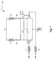
- FIG. 5illustrates an embodiment 500 of a wideband variable delay cell.
- the input of the signalis connected to a current-controlled CMOS (C3MOS) wideband data amplifier circuit having expanded bandwidth that is similar to the embodiment 100 of the FIG. 1 .
- C3MOScurrent-controlled CMOS
- the operation of such a wideband data amplifier circuit having expanded bandwidthis also described in commonly-assigned U.S. patent application Ser. No. 10/028,806, now U.S. Pat. No. 6,624,699 B2, entitled “Current-controlled CMOS wideband data amplifier circuits,” by Guangming Yin and Jun Cao.
- a cross-coupled differential pairConnected to the output of the wideband data buffer having expanded bandwidth (that includes the differential transistor pair M 1 and M 2 , i.e. a wideband differential transistor pair) is a cross-coupled differential pair (that includes the differential transistor pair M 3 and M 4 , i.e. a cross-coupled differential transistor pair) as the regenerative stage for the data.
- this embodiment 500there are therefore two very fast operating blocks [(1) wideband data buffer and (2) cross-coupled differential pair] that operate cooperatively to perform the functionality of a wideband variable delay cell that is appropriate for broadband applications.
- the currents of the buffer stage and the cross-coupled differential pair stagecan be adjusted (e.g., using a control block 530 ).
- the circuitbehaves just like a wideband data amplifier having expanded bandwidth as described and referenced above (i.e., the embodiment 100 of the FIG. 1 and within U.S. Pat. No. 6,624,699 B2).
- the delay through the delay cellcan be very small.
- the current going through the buffer stageis reduced and the current going through the cross-coupled differential pair stage is increased by the same amount.
- a first-order analysis of the embodiment 500 of such a variable delay cellcan be done based on a two-step approximation, as shown below.
- the buffer stage of the variable delay cellSince the buffer stage of the variable delay cell has very high bandwidth, the delay from input to output at this stage is very small. It is reasonable to assume the delay through the buffer stage is a relatively constant value (denoted as T b ); the delay variation of the delay cell is mostly contributed by the regenerative process of the cross-coupled differential pair stage (denoted as T r ).
- the signal through the delay cellis divided into two steps. In the first step, the signal V in is buffered by the input stage and appear at the output after a delay of T 0 , taking a value of V m ⁇ V m is equal to the current passing through the buffer stage (I b ) times the load resistance (R).
- the signal V m at the input of the cross-coupled differential pairgoes through the positive feedback of the cross-coupled differential pair and gets regenerated until reaching the value of V 0 , after a delay of T r .
- ⁇is the characteristic time constant of the cross-coupled differential pair, which is inversely proportional to the gain of the cross-coupled differential pair.
- the gainis proportional to the square root of the biasing current in the first order as indicated below.
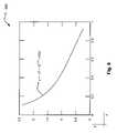
- FIG. 6illustrates an embodiment 600 of delay through a cross-coupled differential pair (normalized) in response to current in a buffer stage (normalized).
- This embodiment 600shows the normalized delay through the cross-coupled differential pair stage, T r /(k ⁇ I 0 ⁇ 0.5 ), as a function of the normalized current in the buffer stage
- the total delay a variable delay cellapproaches the delay of the wideband data buffer (that includes the differential transistor pair M 1 and M 2 ).
- the total delay a variable delay cellapproaches the maximum possible delay of the device that includes the delay of both the wideband data buffer (that includes the differential transistor pair M 1 and M 2 ) and the cross-coupled differential pair (that includes the differential transistor pair M 3 and M 4 ).
- Various embodiments of the invention presented hereinprovide for a large amount of delay to be incurred (which is selectable and variable, as desired in any of a wide variety of applications) with a minimal amount of signal quality degradation (i.e., minimal or no ISI).
- the embodiment 500 of the FIG. 5shows an integrated delay cell that does not require the summing stage and thus reduces the power significantly. There is no extra capacitive loading added to the high speed path at the input. The additional capacitance due to the drains of the cross-coupled differential pair transistors at the output can be easily compensated by the shunt inductor. As a result, it is much easier to incorporate the integrated stage into the data path without compromising the signal integrity or degrading the impedance matching.
- the amount of delaycan be changed continuously by implementing continuous control signals for the two current sources (i.e., using control block 530 ).
- a programmable delay cellcan also be readily implemented by replacing the two current sources (I b and I r ) with a series of smaller current source, each can be turn on or off using digital control signals.
- CMOS (C3MOS) integrated wideband delay cellis presented herein.
- bandwidth extension techniquessuch as shunt peaking, series inductive peaking can be readily applied to increase the range of the flat frequency response.
- a cross-coupled differential pair stageis added to the output of the buffer to add delay from input to output through the regenerative process of the cross-coupled differential transistor pair connected in a positive feedback configuration. The delay can be adjusted by varying the current distribution between the buffer stage and the cross-coupled differential pair stage.
- the integrated delay cellcan then accommodate a large amount of delay while at the same time maintain a high bandwidth for the data path, without adding load to the input and without adding power consumption.
Landscapes
- Physics & Mathematics (AREA)
- Nonlinear Science (AREA)
- Networks Using Active Elements (AREA)
- Pulse Circuits (AREA)
- Amplifiers (AREA)
Abstract
Description
V(t)=Vm·e(t/τ)
It is evident that as the current passing through the buffer stage becomes smaller, the delay through the cross-coupled differential pair stage becomes bigger. The total delay through the delay cell is T=Tb+Tr. Thus by changing the current distribution between the buffer stage (including the differential transistor pair M1 and M2) and cross-coupled differential pair stage (including the differential transistor pair M3 and M4) (i.e., which involves changing the value of x), the amount of the delay can be readily adjusted.
Claims (20)
Priority Applications (4)
| Application Number | Priority Date | Filing Date | Title |
|---|---|---|---|
| US11/320,401US7598788B2 (en) | 2005-09-06 | 2005-12-28 | Current-controlled CMOS (C3MOS) fully differential integrated delay cell with variable delay and high bandwidth |
| EP06008842.4AEP1760885B1 (en) | 2005-09-06 | 2006-04-27 | Current-controlled CMOS (C3MOS) fully differential integrated delay cell with variable delay and high bandwidth |
| TW095127732ATW200721684A (en) | 2005-09-06 | 2006-07-28 | Current-controlled CMOS (C3MOS) fully differential integrated delay cell with variable delay and high bandwidth |
| US12/571,553US20100019817A1 (en) | 2005-09-06 | 2009-10-01 | Current-controlled CMOS (C3MOS) fully differential integrated delay cell with variable delay and high bandwidth |
Applications Claiming Priority (2)
| Application Number | Priority Date | Filing Date | Title |
|---|---|---|---|
| US71481405P | 2005-09-06 | 2005-09-06 | |
| US11/320,401US7598788B2 (en) | 2005-09-06 | 2005-12-28 | Current-controlled CMOS (C3MOS) fully differential integrated delay cell with variable delay and high bandwidth |
Related Child Applications (1)
| Application Number | Title | Priority Date | Filing Date |
|---|---|---|---|
| US12/571,553ContinuationUS20100019817A1 (en) | 2005-09-06 | 2009-10-01 | Current-controlled CMOS (C3MOS) fully differential integrated delay cell with variable delay and high bandwidth |
Publications (2)
| Publication Number | Publication Date |
|---|---|
| US20070052467A1 US20070052467A1 (en) | 2007-03-08 |
| US7598788B2true US7598788B2 (en) | 2009-10-06 |
Family
ID=37459534
Family Applications (2)
| Application Number | Title | Priority Date | Filing Date |
|---|---|---|---|
| US11/320,401Expired - Fee RelatedUS7598788B2 (en) | 2005-09-06 | 2005-12-28 | Current-controlled CMOS (C3MOS) fully differential integrated delay cell with variable delay and high bandwidth |
| US12/571,553AbandonedUS20100019817A1 (en) | 2005-09-06 | 2009-10-01 | Current-controlled CMOS (C3MOS) fully differential integrated delay cell with variable delay and high bandwidth |
Family Applications After (1)
| Application Number | Title | Priority Date | Filing Date |
|---|---|---|---|
| US12/571,553AbandonedUS20100019817A1 (en) | 2005-09-06 | 2009-10-01 | Current-controlled CMOS (C3MOS) fully differential integrated delay cell with variable delay and high bandwidth |
Country Status (3)
| Country | Link |
|---|---|
| US (2) | US7598788B2 (en) |
| EP (1) | EP1760885B1 (en) |
| TW (1) | TW200721684A (en) |
Cited By (15)
| Publication number | Priority date | Publication date | Assignee | Title |
|---|---|---|---|---|
| US20120038390A1 (en)* | 2010-08-16 | 2012-02-16 | Broadcom Corporation | Gigabit-speed slicer latch with hysteresis optimization |
| US20120139631A1 (en)* | 2010-12-07 | 2012-06-07 | Wong Thomas Y | Wide-swing telescopic operational amplifier |
| US20120306288A1 (en)* | 2011-06-06 | 2012-12-06 | National University Corporation Toyohashi University Of Technology | Switching circuit |
| US20130229232A1 (en)* | 2011-06-22 | 2013-09-05 | Broadcom Corporation | Amplifier Bandwidth Extension for High-Speed Tranceivers |
| US8614604B2 (en)* | 2011-12-06 | 2013-12-24 | Taiwan Semiconductor Manufacturing Company, Ltd. | Amplifier inductor sharing for inductive peaking |
| US8773187B2 (en)* | 2010-09-16 | 2014-07-08 | Micron Technology, Inc. | Analog delay lines and adaptive biasing |
| US9148087B1 (en)* | 2014-05-16 | 2015-09-29 | Kandou Labs, S.A. | Symmetric is linear equalization circuit with increased gain |
| US9438176B2 (en) | 2013-04-19 | 2016-09-06 | Industry-Academic Cooperation Foundation, Yonsei University | Low noise amplifier |
| US9595975B1 (en) | 2015-09-30 | 2017-03-14 | Samsung Display Co., Ltd. | Low-latency high-gain current-mode logic slicer |
| US9602314B1 (en) | 2016-02-10 | 2017-03-21 | Nxp Usa, Inc. | Communications receiver equalizer |
| US9654310B1 (en)* | 2016-11-19 | 2017-05-16 | Nxp Usa, Inc. | Analog delay cell and tapped delay line comprising the analog delay cell |
| US20170141763A1 (en)* | 2015-11-18 | 2017-05-18 | Electronics And Telecommunications Research Institute | Frequency doubler having optimized harmonic suppression characteristics |
| US9887552B2 (en)* | 2013-03-14 | 2018-02-06 | Analog Devices, Inc. | Fine timing adjustment method |
| US10680591B2 (en) | 2018-04-02 | 2020-06-09 | Hewlett Packard Enterprise Development Lp | Programmable resistive delay |
| US11075779B2 (en)* | 2018-03-30 | 2021-07-27 | Intel Corporation | Transceiver baseband processing |
Families Citing this family (6)
| Publication number | Priority date | Publication date | Assignee | Title |
|---|---|---|---|---|
| US20090179670A1 (en)* | 2008-01-15 | 2009-07-16 | International Business Machines Corporation | Performance inversion detection circuit and a design structure for the same |
| US8248135B2 (en)* | 2010-01-15 | 2012-08-21 | Integrated Device Technology, Inc. | Circuit including current-mode logic driver with multi-rate programmable pre-emphasis delay element |
| DE102010025782A1 (en)* | 2010-07-01 | 2012-01-05 | Rohde & Schwarz Gmbh & Co. Kg | Electronic circuit for optical control of a flip-flop |
| JP5891492B2 (en)* | 2011-06-22 | 2016-03-23 | 株式会社Joled | Display element, display device, and electronic device |
| US12265483B2 (en)* | 2020-12-02 | 2025-04-01 | Intel Corporation | Shunt-series and series-shunt inductively peaked clock buffer, and asymmetric multiplexer and de-multiplexer |
| US12184751B2 (en)* | 2020-12-18 | 2024-12-31 | Intel Corporation | Wide-range inductor-based delay-cell and area efficient termination switch control |
Citations (189)
| Publication number | Priority date | Publication date | Assignee | Title |
|---|---|---|---|---|
| US3569732A (en) | 1969-12-15 | 1971-03-09 | Shell Oil Co | Inductanceless igfet frequency doubler |
| WO1981001780A1 (en) | 1979-12-10 | 1981-06-25 | Gen Electric | Bandpass amplifier circuits |
| US4333020A (en) | 1979-05-23 | 1982-06-01 | Motorola, Inc. | MOS Latch circuit |
| US4395774A (en) | 1981-01-12 | 1983-07-26 | National Semiconductor Corporation | Low power CMOS frequency divider |
| US4449248A (en) | 1982-02-01 | 1984-05-15 | General Electric Company | Battery saving radio circuit and system |
| US4519068A (en) | 1983-07-11 | 1985-05-21 | Motorola, Inc. | Method and apparatus for communicating variable length messages between a primary station and remote stations of a data communications system |
| US4545023A (en) | 1980-11-14 | 1985-10-01 | Engineering Project Development Limited | Hand-held computer |
| US4599526A (en) | 1983-05-13 | 1986-07-08 | At&T Bell Laboratories | Clocked latching circuit |
| US4649293A (en) | 1984-11-09 | 1987-03-10 | U.S. Philips Corporation | Clocked comparator |
| US4680787A (en) | 1984-11-21 | 1987-07-14 | Motorola, Inc. | Portable radiotelephone vehicular converter and remote handset |
| US4727309A (en) | 1987-01-22 | 1988-02-23 | Intel Corporation | Current difference current source |
| US4731796A (en) | 1984-10-25 | 1988-03-15 | Stc, Plc | Multi-mode radio transceiver |
| US4737975A (en) | 1984-09-18 | 1988-04-12 | Metrofone, Inc. | Programmable system for interfacing a standard telephone set with a radio transceiver |
| US4761822A (en) | 1985-08-23 | 1988-08-02 | Libera Developments Ltd. | Burst-mode two-way radio communications system |
| US4777657A (en) | 1987-04-01 | 1988-10-11 | Iss Engineering, Inc. | Computer controlled broadband receiver |
| US4794649A (en) | 1986-05-06 | 1988-12-27 | Nec Corporation | Radio communication system with power saving disablement prior to call handling processes |
| US4804954A (en) | 1987-04-30 | 1989-02-14 | Motorola, Inc. | Battery saving method for portable communications receivers |
| US4807282A (en) | 1985-12-30 | 1989-02-21 | International Business Machines Corp. | Programmable P/C compatible communications card |
| US4806796A (en) | 1988-03-28 | 1989-02-21 | Motorola, Inc. | Active load for emitter coupled logic gate |
| US4817115A (en) | 1987-02-27 | 1989-03-28 | Telxon Corporation | Encoding and decoding system for electronic data communication system |
| US4850009A (en) | 1986-05-12 | 1989-07-18 | Clinicom Incorporated | Portable handheld terminal including optical bar code reader and electromagnetic transceiver means for interactive wireless communication with a base communications station |
| US4890832A (en) | 1982-10-13 | 1990-01-02 | Sharp Kabushiki Kaisha | Compact electronic apparatus with removable processing units |
| US4894792A (en) | 1988-09-30 | 1990-01-16 | Tandy Corporation | Portable computer with removable and replaceable add-on modules |
| US4916441A (en) | 1988-09-19 | 1990-04-10 | Clinicom Incorporated | Portable handheld terminal |
| US4964121A (en) | 1989-08-30 | 1990-10-16 | Motorola, Inc. | Battery saver for a TDM system |
| US4969206A (en) | 1989-07-18 | 1990-11-06 | Phyle Industries Limited | Portable data collection device with RF transmission |
| US4970406A (en) | 1987-12-30 | 1990-11-13 | Gazelle Microcircuits, Inc. | Resettable latch circuit |
| US4977611A (en) | 1987-02-20 | 1990-12-11 | Nec Corporation | Portable radio apparatus having battery saved channel scanning function |
| US4995099A (en) | 1988-12-01 | 1991-02-19 | Motorola, Inc. | Power conservation method and apparatus for a portion of a predetermined signal |
| US5008879A (en) | 1988-11-14 | 1991-04-16 | Datapoint Corporation | LAN with interoperative multiple operational capabilities |
| US5025486A (en) | 1988-12-09 | 1991-06-18 | Dallas Semiconductor Corporation | Wireless communication system with parallel polling |
| US5029183A (en) | 1989-06-29 | 1991-07-02 | Symbol Technologies, Inc. | Packet data communication network |
| US5031231A (en) | 1988-09-26 | 1991-07-09 | Nec Corporation | Mobile telephone station with power saving circuit |
| US5033109A (en) | 1988-07-01 | 1991-07-16 | Mitsubishi Denki Kabushiki Kaisha | Pocket transceiver |
| US5041740A (en) | 1990-04-30 | 1991-08-20 | Motorola, Inc. | Parallel clocked latch |
| US5055660A (en) | 1988-06-16 | 1991-10-08 | Avicom International, Inc. | Portable transaction monitoring unit for transaction monitoring and security control systems |
| US5055659A (en) | 1990-02-06 | 1991-10-08 | Amtech Technology Corp. | High speed system for reading and writing data from and into remote tags |
| US5079452A (en) | 1990-06-29 | 1992-01-07 | Digital Equipment Corporation | High speed ECL latch with clock enable |
| US5081402A (en) | 1991-02-22 | 1992-01-14 | Comfortex Corporation | Low power consumption wireless data transmission and control system |
| US5087099A (en) | 1988-09-02 | 1992-02-11 | Stolar, Inc. | Long range multiple point wireless control and monitoring system |
| US5115151A (en) | 1990-06-08 | 1992-05-19 | Western Digital Corporation | Triple comparator circuit |
| US5117501A (en) | 1988-08-08 | 1992-05-26 | General Electric Company | Dynamic regrouping in a trunked radio communications system |
| US5119502A (en) | 1990-08-30 | 1992-06-02 | Telefonaktiebolaget L M Ericsson | Periodic system ordered rescan in a cellular communication system |
| US5121408A (en) | 1989-10-16 | 1992-06-09 | Hughes Aircraft Company | Synchronization for entry to a network in a frequency hopping communication system |
| US5123029A (en) | 1991-06-21 | 1992-06-16 | International Business Machines Corporation | Broadcast-initiated bipartite frame multi-access protocol |
| US5128938A (en) | 1989-03-03 | 1992-07-07 | Motorola, Inc. | Energy saving protocol for a communication system |
| US5134347A (en) | 1991-02-22 | 1992-07-28 | Comfortex Corporation | Low power consumption wireless data transmission and control system |
| US5142573A (en) | 1990-02-08 | 1992-08-25 | Oki Electric Industry Co., Ltd. | Telephone apparatus for radio communication with an adaptor |
| US5150361A (en) | 1989-01-23 | 1992-09-22 | Motorola, Inc. | Energy saving protocol for a TDM radio |
| US5152006A (en) | 1991-02-25 | 1992-09-29 | Motorola, Inc. | Receiver controller method and apparatus |
| US5153878A (en) | 1989-12-11 | 1992-10-06 | Motorola Inc. | Radio data communications system with diverse signaling capability |
| US5175870A (en) | 1988-12-23 | 1992-12-29 | U.S. Philips Corporation | Power economising in multiple user radio systems |
| US5177378A (en) | 1990-05-08 | 1993-01-05 | Kabushiki Kaisha Toshiba | Source-coupled FET logic circuit |
| US5179721A (en) | 1990-11-05 | 1993-01-12 | Motorola Inc. | Method for inter operation of a cellular communication system and a trunking communication system |
| US5181200A (en) | 1990-10-29 | 1993-01-19 | International Business Machines Corporation | Handoff method and apparatus for mobile wireless workstation |
| US5196805A (en)* | 1992-01-31 | 1993-03-23 | Motorola, Inc. | Distributed differential amplifier arrangement |
| US5216295A (en)* | 1991-08-30 | 1993-06-01 | General Instrument Corp. | Current mode logic circuits employing IGFETS |
| US5230084A (en) | 1990-12-06 | 1993-07-20 | Motorola, Inc. | Selective call receiver having extended battery saving capability |
| US5239662A (en) | 1986-09-15 | 1993-08-24 | Norand Corporation | System including multiple device communications controller which coverts data received from two different customer transaction devices each using different communications protocols into a single communications protocol |
| US5241542A (en) | 1991-08-23 | 1993-08-31 | International Business Machines Corporation | Battery efficient operation of scheduled access protocol |
| US5241691A (en) | 1990-03-09 | 1993-08-31 | U.S. Philips Corporation | Method of optimizing the transmission of idle beacon messages and a communications system using the method |
| US5247656A (en) | 1989-06-01 | 1993-09-21 | Matsushita Electric Industrial Co., Ltd. | Method and apparatus for controlling a clock signal |
| US5249302A (en) | 1987-10-09 | 1993-09-28 | Motorola, Inc. | Mixed-mode transceiver system |
| US5249220A (en) | 1991-04-18 | 1993-09-28 | Rts Electronics, Inc. | Handheld facsimile and alphanumeric message transceiver operating over telephone or wireless networks |
| US5265270A (en) | 1990-10-31 | 1993-11-23 | Motorola, Inc. | Method and apparatus for providing power conservation in a communication system |
| US5265238A (en) | 1991-01-25 | 1993-11-23 | International Business Machines Corporation | Automatic device configuration for dockable portable computers |
| US5274666A (en) | 1991-10-16 | 1993-12-28 | Telephonics Corporation | Wireless communication system |
| US5276680A (en) | 1991-04-11 | 1994-01-04 | Telesystems Slw Inc. | Wireless coupling of devices to wired network |
| US5278831A (en) | 1991-07-09 | 1994-01-11 | U.S. Philips Corporation | Information transmission system |
| US5289055A (en) | 1992-11-17 | 1994-02-22 | At&T Bell Laboratories | Digital ECL bipolar logic gates suitable for low-voltage operation |
| US5289469A (en) | 1991-01-17 | 1994-02-22 | Kabushiki Kaisha Toshiba | Communication control unit with lower layer protocol control and higher layer protocol control |
| US5291516A (en) | 1991-05-13 | 1994-03-01 | Omnipoint Data Company, Inc. | Dual mode transmitter and receiver |
| US5293639A (en) | 1991-08-09 | 1994-03-08 | Motorola, Inc. | Reduction of power consumption in a portable communication unit |
| US5296849A (en) | 1990-10-25 | 1994-03-22 | Nec Corporation | Pager receiver for enabling to omit power-on signal for receiving synchronization code in pager signal |
| US5297144A (en) | 1991-01-22 | 1994-03-22 | Spectrix Corporation | Reservation-based polling protocol for a wireless data communications network |
| US5301196A (en) | 1992-03-16 | 1994-04-05 | International Business Machines Corporation | Half-speed clock recovery and demultiplexer circuit |
| US5323392A (en) | 1991-03-13 | 1994-06-21 | International Business Machines Corporation | Adaptation device and method for efficient interconnection of data processing devices and networks |
| US5331509A (en) | 1992-06-29 | 1994-07-19 | Cordata, Inc. | Modular notebook computer having a planar array of module bays and a pivotally attached flat-panel display |
| US5345449A (en) | 1989-07-07 | 1994-09-06 | Inmos Limited | Clock generation |
| US5349649A (en) | 1991-04-22 | 1994-09-20 | Kabushiki Kaisha Toshiba | Portable electronic device supporting multi-protocols |
| US5361397A (en) | 1991-08-26 | 1994-11-01 | Motorola, Inc. | Communication device and system capable of automatic programmable energizing |
| US5363121A (en) | 1990-06-29 | 1994-11-08 | International Business Machines Corporation | Multiple protocol communication interface for distributed transaction processing |
| US5373149A (en) | 1993-02-01 | 1994-12-13 | At&T Bell Laboratories | Folding electronic card assembly |
| US5373506A (en) | 1990-11-26 | 1994-12-13 | Motorola Inc. | Method and apparatus for paging in a communication system |
| US5390206A (en) | 1991-10-01 | 1995-02-14 | American Standard Inc. | Wireless communication system for air distribution system |
| US5392023A (en) | 1991-09-06 | 1995-02-21 | Motorola, Inc. | Data communication system with automatic power control |
| US5406643A (en) | 1993-02-11 | 1995-04-11 | Motorola, Inc. | Method and apparatus for selecting between a plurality of communication paths |
| US5406615A (en) | 1993-08-04 | 1995-04-11 | At&T Corp. | Multi-band wireless radiotelephone operative in a plurality of air interface of differing wireless communications systems |
| US5418837A (en) | 1993-07-30 | 1995-05-23 | Ericsson-Ge Mobile Communications Inc. | Method and apparatus for upgrading cellular mobile telephones |
| US5420529A (en) | 1994-05-19 | 1995-05-30 | Northern Telecom Limited | Current steering switch and hybrid BiCMOS multiplexer with CMOS commutation signal and CML/ECL data signals |
| US5423002A (en) | 1992-04-20 | 1995-06-06 | 3Com Corporation | System for extending network resources to remote networks |
| US5426637A (en) | 1992-12-14 | 1995-06-20 | International Business Machines Corporation | Methods and apparatus for interconnecting local area networks with wide area backbone networks |
| US5428636A (en) | 1993-05-03 | 1995-06-27 | Norand Corporation | Radio frequency local area network |
| US5430845A (en) | 1990-06-07 | 1995-07-04 | Unisys Corporation | Peripheral device interface for dynamically selecting boot disk device driver |
| US5434518A (en) | 1992-10-02 | 1995-07-18 | National Semiconductor Corporation | ECL-to-BICOMS/CMOS translator |
| US5438329A (en) | 1993-06-04 | 1995-08-01 | M & Fc Holding Company, Inc. | Duplex bi-directional multi-mode remote instrument reading and telemetry system |
| US5440560A (en) | 1991-12-24 | 1995-08-08 | Rypinski; Chandos A. | Sleep mode and contention resolution within a common channel medium access method |
| US5457412A (en) | 1992-11-17 | 1995-10-10 | Hitachi, Ltd. | Semiconductor integrated circuit device including input circuitry to permit operation of a Bi-CMOS memory with ECL level input signals |
| US5459412A (en) | 1993-07-01 | 1995-10-17 | National Semiconductor Corporation | BiCMOS circuit for translation of ECL logic levels to MOS logic levels |
| US5465081A (en) | 1990-03-03 | 1995-11-07 | Cedar-Dell Limited | Multicomponent wireless system with periodic shutdown of transmitting and receiving modes |
| US5481562A (en) | 1989-11-03 | 1996-01-02 | Microcom Systems, Inc. | Multi-mode modem and data transmission method |
| US5481265A (en) | 1989-11-22 | 1996-01-02 | Russell; David C. | Ergonomic customizeable user/computer interface devices |
| US5510734A (en) | 1994-06-14 | 1996-04-23 | Nec Corporation | High speed comparator having two differential amplifier stages and latch stage |
| US5510748A (en) | 1994-01-18 | 1996-04-23 | Vivid Semiconductor, Inc. | Integrated circuit having different power supplies for increased output voltage range while retaining small device geometries |
| US5521530A (en) | 1994-08-31 | 1996-05-28 | Oki Semiconductor America, Inc. | Efficient method and resulting structure for integrated circuits with flexible I/O interface and power supply voltages |
| US5526314A (en)* | 1994-12-09 | 1996-06-11 | International Business Machines Corporation | Two mode sense amplifier with latch |
| US5533029A (en) | 1993-11-12 | 1996-07-02 | Pacific Communication Sciences, Inc. | Cellular digital packet data mobile data base station |
| US5535373A (en) | 1991-11-27 | 1996-07-09 | International Business Machines Corporation | Protocol-to-protocol translator for interfacing disparate serial network nodes to a common parallel switching network |
| US5548230A (en) | 1994-05-31 | 1996-08-20 | Pmc-Sierra, Inc. | High-speed CMOS pseudo-ECL output driver |
| US5576644A (en) | 1994-06-10 | 1996-11-19 | International Business Machines Corporation | Fast edge triggered self-resetting CMOS receiver with parallel L1/L2 (master/slave) latch |
| US5579487A (en) | 1992-10-02 | 1996-11-26 | Teletransaction, Inc. | Portable work slate computer with multiple docking positions for interchangeably receiving removable modules |
| US5584048A (en) | 1990-08-17 | 1996-12-10 | Motorola, Inc. | Beacon based packet radio standby energy saver |
| US5600267A (en) | 1994-06-24 | 1997-02-04 | Cypress Semiconductor Corporation | Apparatus for a programmable CML to CMOS translator for power/speed adjustment |
| US5606268A (en) | 1993-03-24 | 1997-02-25 | Apple Computer, Inc. | Differential to single-ended CMOS converter |
| US5614841A (en) | 1993-12-24 | 1997-03-25 | Bull S.A. | Frequency multiplier using XOR/NXOR gates which have equal propagation delays |
| US5625308A (en)* | 1995-06-08 | 1997-04-29 | Mitsubishi Denki Kabushiki Kaisha | Two input-two output differential latch circuit |
| US5630061A (en) | 1993-04-19 | 1997-05-13 | International Business Machines Corporation | System for enabling first computer to communicate over switched network with second computer located within LAN by using media access control driver in different modes |
| US5640356A (en) | 1995-12-29 | 1997-06-17 | Cypress Semiconductor Corp. | Two-stage differential sense amplifier with positive feedback in the first and second stages |
| US5675584A (en) | 1994-06-06 | 1997-10-07 | Sun Microsystems, Inc. | High speed serial link for fully duplexed data communication |
| US5680633A (en) | 1990-01-18 | 1997-10-21 | Norand Corporation | Modular, portable data processing terminal for use in a radio frequency communication network |
| US5708399A (en) | 1995-09-13 | 1998-01-13 | Fujitsu Limited | Modulator and frequency multiplier for use therein |
| US5724361A (en) | 1996-03-12 | 1998-03-03 | Lsi Logic Corporation | High performance n:1 multiplexer with overlap control of multi-phase clocks |
| US5732346A (en) | 1993-06-17 | 1998-03-24 | Research In Motion Limited | Translation and connection device for radio frequency point of sale transaction systems |
| US5740366A (en) | 1991-10-01 | 1998-04-14 | Norand Corporation | Communication network having a plurality of bridging nodes which transmit a beacon to terminal nodes in power saving state that it has messages awaiting delivery |
| US5744366A (en) | 1992-05-01 | 1998-04-28 | Trustees Of The University Of Pennsylvania | Mesoscale devices and methods for analysis of motile cells |
| US5767699A (en) | 1996-05-28 | 1998-06-16 | Sun Microsystems, Inc. | Fully complementary differential output driver for high speed digital communications |
| US5796727A (en) | 1993-04-30 | 1998-08-18 | International Business Machines Corporation | Wide-area wireless lan access |
| US5798658A (en) | 1995-06-15 | 1998-08-25 | Werking; Paul M. | Source-coupled logic with reference controlled inputs |
| US5821809A (en) | 1996-05-23 | 1998-10-13 | International Business Machines Corporation | CMOS high-speed differential to single-ended converter circuit |
| US5839051A (en) | 1989-03-17 | 1998-11-17 | Technophone Limited | Host radio telephone to directly access a handset NAM through a connecter without requiring the handset controller to be employed |
| US5877642A (en) | 1995-11-17 | 1999-03-02 | Nec Corporation | Latch circuit for receiving small amplitude signals |
| US5892382A (en) | 1997-03-25 | 1999-04-06 | Mitsubishi Denki Kabushiki Kaisha | Current mode logic circuit, source follower circuit and flip flop circuit |
| US5903176A (en) | 1996-09-04 | 1999-05-11 | Litton Systems, Inc. | Clock circuit for generating a high resolution output from a low resolution clock |
| US5905386A (en) | 1996-01-02 | 1999-05-18 | Pmc-Sierra Ltd. | CMOS SONET/ATM receiver suitable for use with pseudo ECL and TTL signaling environments |
| US5940771A (en) | 1991-05-13 | 1999-08-17 | Norand Corporation | Network supporting roaming, sleeping terminals |
| US5945847A (en)* | 1997-05-20 | 1999-08-31 | Lucent Technologies | Distributed amplifier logic designs |
| US5945858A (en) | 1997-03-31 | 1999-08-31 | Nec Corporation | Clocked flip flop circuit with built-in clock controller and frequency divider using the same |
| US5945863A (en) | 1997-06-18 | 1999-08-31 | Applied Micro Circuits Corporation | Analog delay circuit |
| US5969556A (en) | 1997-03-05 | 1999-10-19 | Mitsubishi Denki Kabushiki Kaisha | Flip-flop circuit, parallel-serial converting circuit, and latch circuit |
| US5994939A (en)* | 1998-01-14 | 1999-11-30 | Intel Corporation | Variable delay cell with a self-biasing load |
| US6002279A (en) | 1997-10-24 | 1999-12-14 | G2 Networks, Inc. | Clock recovery circuit |
| US6014041A (en) | 1997-09-26 | 2000-01-11 | Intel Corporation | Differential current switch logic gate |
| US6014705A (en) | 1991-10-01 | 2000-01-11 | Intermec Ip Corp. | Modular portable data processing terminal having a higher layer and lower layer partitioned communication protocol stack for use in a radio frequency communications network |
| EP0685933B1 (en) | 1994-06-02 | 2000-01-12 | Mitsubishi Denki Kabushiki Kaisha | Differential amplifier |
| US6028454A (en) | 1997-04-11 | 2000-02-22 | The University Of Waterloo | Dynamic current mode logic family |
| US6037841A (en) | 1997-10-07 | 2000-03-14 | Applied Micro Circuits Corporation | Impedance matched CMOS transimpedance amplifier for high-speed fiber optic communications |
| US6037842A (en) | 1998-04-21 | 2000-03-14 | Applied Micro Circuits Corporation | Complementary metal-oxide semiconductor voltage controlled oscillator (CMOS VCO) |
| US6038254A (en) | 1996-06-07 | 2000-03-14 | International Business Machines Corporation | Adaptive filtering method and apparatus to compensate for a frequency difference between two clock sources |
| US6060951A (en) | 1998-06-02 | 2000-05-09 | Mitsubishi Denki Kabushiki Kaisha | Semiconductor device |
| US6061747A (en) | 1997-10-16 | 2000-05-09 | Lsi Logic Corporation | System for sending data from-and-to a computer monitor using a high speed serial line |
| US6081162A (en) | 1999-06-17 | 2000-06-27 | Intel Corporation | Robust method and apparatus for providing a digital single-ended output from a differential input |
| US6094074A (en) | 1998-07-16 | 2000-07-25 | Seiko Epson Corporation | High speed common mode logic circuit |
| US6111425A (en) | 1998-10-15 | 2000-08-29 | International Business Machines Corporation | Very low power logic circuit family with enhanced noise immunity |
| US6114843A (en) | 1998-08-18 | 2000-09-05 | Xilinx, Inc. | Voltage down converter for multiple voltage levels |
| US6188339B1 (en) | 1998-01-23 | 2001-02-13 | Fuji Photo Film Co., Ltd. | Differential multiplexer and differential logic circuit |
| US6194950B1 (en) | 1997-08-28 | 2001-02-27 | Lucent Technologies Inc. | High-speed CMOS multiplexer |
| US6222380B1 (en) | 1998-06-15 | 2001-04-24 | International Business Machines Corporation | High speed parallel/serial link for data communication |
| US6232844B1 (en) | 1999-05-28 | 2001-05-15 | Vitesse Semiconductor Corporation | Controlled orthogonal current oscillator with ranging |
| US6255881B1 (en)* | 1998-11-26 | 2001-07-03 | Cselt- Centro Studi E Laboratori Telecomunicazioni S.P.A. | High tunability CMOS delay element |
| US6259321B1 (en) | 1999-11-23 | 2001-07-10 | Electronics And Telecommunications Research Institute | CMOS variable gain amplifier and control method therefor |
| US6259312B1 (en) | 1998-03-11 | 2001-07-10 | Nokia Mobile Phones Limited | Circuit arrangement for adjusting the impedance of a differential active component |
| US6265898B1 (en) | 1998-07-13 | 2001-07-24 | Texas Instruments Incorporated | Current mode logic gates for low-voltage high speed applications |
| WO2001063767A2 (en) | 2000-02-24 | 2001-08-30 | Broadcom Corporation | Current-controlled cmos circuits with inductive broadbanding |
| US6310501B1 (en) | 1998-11-27 | 2001-10-30 | Nec Corporation | Latch circuit for latching data at an edge of a clock signal |
| US6320422B1 (en)* | 1999-11-23 | 2001-11-20 | National Semiconductor Corporation | Complementary source coupled logic |
| US6366166B1 (en) | 1999-08-31 | 2002-04-02 | Stmicroelectronics S.A. | Double pass band amplifier circuit and a radio frequency reception head |
| US6374311B1 (en) | 1991-10-01 | 2002-04-16 | Intermec Ip Corp. | Communication network having a plurality of bridging nodes which transmit a beacon to terminal nodes in power saving state that it has messages awaiting delivery |
| US6377095B1 (en)* | 2000-10-10 | 2002-04-23 | National Semiconductor Corporation | Digital-edge-rate control LVDS driver |
| US6414558B1 (en) | 1999-05-12 | 2002-07-02 | Parthus Ireland Limited | Method and apparatus for random sequence generator |
| US6417737B1 (en)* | 1999-10-21 | 2002-07-09 | Broadcom Corporation | Adaptive radio transceiver with low noise amplification |
| US6424194B1 (en) | 1999-06-28 | 2002-07-23 | Broadcom Corporation | Current-controlled CMOS logic family |
| US6429692B1 (en)* | 2001-06-19 | 2002-08-06 | Octillion Communications, Inc. | High speed data sampling with reduced metastability |
| US6456122B1 (en)* | 2000-08-18 | 2002-09-24 | Samsung Electronics, Co., Ltd. | Input buffer circuit for transforming pseudo differential signals into full differential signals |
| US6462590B2 (en)* | 1999-07-01 | 2002-10-08 | Vitesse Semiconductor Corporation | High bandwidth clock buffer |
| US6463092B1 (en) | 1998-09-10 | 2002-10-08 | Silicon Image, Inc. | System and method for sending and receiving data signals over a clock signal line |
| US20030034843A1 (en) | 2001-08-15 | 2003-02-20 | Adel Fanous | System and method for activating gain stages in an amplification module |
| EP1306970A2 (en) | 2001-10-25 | 2003-05-02 | Broadcom Corporation | Current-controlled CMOS wideband amplifier circuits |
| US6559693B2 (en)* | 2001-09-05 | 2003-05-06 | John C. Tung | Integrated circuit designs for high speed signal processing |
| US6566720B2 (en) | 2000-10-05 | 2003-05-20 | United Memories, Inc. | Base cell layout permitting rapid layout with minimum clock line capacitance on CMOS standard-cell and gate-array integrated circuits |
| US6686787B2 (en)* | 2002-02-28 | 2004-02-03 | Kuok Ling | High-speed fully balanced differential flip-flop with reset |
| US6686788B2 (en)* | 2001-06-30 | 2004-02-03 | Hynix Semiconductor Inc. | Delay circuit of clock synchronization device using delay cells having wide delay range |
| US20040104746A1 (en) | 2002-09-30 | 2004-06-03 | Integrant Technologies Inc. | Transconductance varying circuit of transconductor circuit, varying bandwidth filter circuit using the same and digital tuning circuit of transconductor-capacitor filter |
| US6774721B1 (en) | 2003-03-07 | 2004-08-10 | Quake Technologies, Inc. | High speed logic circuits |
| US20050015638A1 (en) | 2001-07-19 | 2005-01-20 | Bo Zhang | Synchronous data serialization circuit |
| US6864558B2 (en) | 2001-05-17 | 2005-03-08 | Broadcom Corporation | Layout technique for C3MOS inductive broadbanding |
| US20050093628A1 (en) | 2003-11-04 | 2005-05-05 | Mitsubishi Denki Kabushiki Kaisha | Differential amplifier circuit and multistage amplifier circuit |
| US20050110525A1 (en) | 2003-11-20 | 2005-05-26 | Mitsubishi Denki Kabushiki Kaisha | Current-mode logic circuit |
| US6911857B1 (en)* | 2002-11-26 | 2005-06-28 | Cypress Semiconductor Corporation | Current controlled delay circuit |
| US7256646B2 (en)* | 2005-06-21 | 2007-08-14 | Seiko Epson Corporation | Neutralization techniques for differential low noise amplifiers |
Family Cites Families (26)
| Publication number | Priority date | Publication date | Assignee | Title |
|---|---|---|---|---|
| US4817054A (en)* | 1985-12-04 | 1989-03-28 | Advanced Micro Devices, Inc. | High speed RAM based data serializers |
| US4727424A (en)* | 1986-10-16 | 1988-02-23 | Rca Corporation | Sampled data filtering system, including a crossbar switch matrix, as for a ghost cancellation system |
| JPS63270435A (en)* | 1987-04-28 | 1988-11-08 | Mitsui Eng & Shipbuild Co Ltd | High corrosion resistant amorphous alloy |
| US5486240A (en)* | 1994-04-25 | 1996-01-23 | Iowa State University Research Foundation, Inc. | Carbide/nitride grain refined rare earth-iron-boron permanent magnet and method of making |
| US5488319A (en)* | 1994-08-18 | 1996-01-30 | International Business Machines Corporation | Latch interface for self-reset logic |
| US5626691A (en)* | 1995-09-11 | 1997-05-06 | The University Of Virginia Patent Foundation | Bulk nanocrystalline titanium alloys with high strength |
| US5690889A (en)* | 1996-02-15 | 1997-11-25 | Iowa State University Research Foundation, Inc. | Production method for making rare earth compounds |
| US5859669A (en)* | 1996-11-26 | 1999-01-12 | Texas Instruments Incorporated | System for encoding an image control signal onto a pixel clock signal |
| US6261386B1 (en)* | 1997-06-30 | 2001-07-17 | Wisconsin Alumni Research Foundation | Nanocrystal dispersed amorphous alloys |
| US6125912A (en)* | 1998-02-02 | 2000-10-03 | Bechtel Bwxt Idaho, Llc | Advanced neutron absorber materials |
| US6258185B1 (en)* | 1999-05-25 | 2001-07-10 | Bechtel Bwxt Idaho, Llc | Methods of forming steel |
| US6265944B1 (en)* | 1999-09-27 | 2001-07-24 | Conexant Systems, Inc. | Fully integrated broadband RF voltage amplifier with enhanced voltage gain and method |
| US6767419B1 (en)* | 2000-11-09 | 2004-07-27 | Bechtel Bwxt Idaho, Llc | Methods of forming hardened surfaces |
| US6689234B2 (en)* | 2000-11-09 | 2004-02-10 | Bechtel Bwxt Idaho, Llc | Method of producing metallic materials |
| US6562156B2 (en)* | 2001-08-02 | 2003-05-13 | Ut-Battelle, Llc | Economic manufacturing of bulk metallic glass compositions by microalloying |
| JP2005517808A (en)* | 2002-02-11 | 2005-06-16 | ユニヴァースティ オブ ヴァージニア パテント ファウンデイション | Bulk-solidifying high manganese non-ferromagnetic amorphous steel alloys and related methods using and manufacturing the same |
| US6597212B1 (en)* | 2002-03-12 | 2003-07-22 | Neoaxiom Corporation | Divide-by-N differential phase interpolator |
| US20040153681A1 (en)* | 2002-11-12 | 2004-08-05 | Broadcom Corporation | Phase detector for extended linear response and high-speed data regeneration |
| CN100427625C (en)* | 2003-02-11 | 2008-10-22 | 纳米钢公司 | Highly active liquid melts used to form coatings |
| WO2004072313A2 (en)* | 2003-02-11 | 2004-08-26 | The Nanosteel Company | Formation of metallic thermal barrier alloys |
| AU2004213409B2 (en)* | 2003-02-14 | 2009-11-05 | The Nanosteel Company, Inc. | Improved properties of amorphous/partially crystalline coatings |
| JP2006519927A (en)* | 2003-02-14 | 2006-08-31 | ザ・ナノスティール・カンパニー | Method for modifying iron-based glass to increase crystallization temperature without changing melting temperature |
| US7604965B2 (en)* | 2003-04-03 | 2009-10-20 | Fluidigm Corporation | Thermal reaction device and method for using the same |
| US7666361B2 (en)* | 2003-04-03 | 2010-02-23 | Fluidigm Corporation | Microfluidic devices and methods of using same |
| US7476363B2 (en)* | 2003-04-03 | 2009-01-13 | Fluidigm Corporation | Microfluidic devices and methods of using same |
| US7400183B1 (en)* | 2005-05-05 | 2008-07-15 | Cypress Semiconductor Corporation | Voltage controlled oscillator delay cell and method |
- 2005
- 2005-12-28USUS11/320,401patent/US7598788B2/ennot_activeExpired - Fee Related
- 2006
- 2006-04-27EPEP06008842.4Apatent/EP1760885B1/ennot_activeCeased
- 2006-07-28TWTW095127732Apatent/TW200721684A/enunknown
- 2009
- 2009-10-01USUS12/571,553patent/US20100019817A1/ennot_activeAbandoned
Patent Citations (195)
| Publication number | Priority date | Publication date | Assignee | Title |
|---|---|---|---|---|
| US3569732A (en) | 1969-12-15 | 1971-03-09 | Shell Oil Co | Inductanceless igfet frequency doubler |
| US4333020A (en) | 1979-05-23 | 1982-06-01 | Motorola, Inc. | MOS Latch circuit |
| WO1981001780A1 (en) | 1979-12-10 | 1981-06-25 | Gen Electric | Bandpass amplifier circuits |
| US4545023A (en) | 1980-11-14 | 1985-10-01 | Engineering Project Development Limited | Hand-held computer |
| US4395774A (en) | 1981-01-12 | 1983-07-26 | National Semiconductor Corporation | Low power CMOS frequency divider |
| US4449248A (en) | 1982-02-01 | 1984-05-15 | General Electric Company | Battery saving radio circuit and system |
| US4890832A (en) | 1982-10-13 | 1990-01-02 | Sharp Kabushiki Kaisha | Compact electronic apparatus with removable processing units |
| US4599526A (en) | 1983-05-13 | 1986-07-08 | At&T Bell Laboratories | Clocked latching circuit |
| US4519068A (en) | 1983-07-11 | 1985-05-21 | Motorola, Inc. | Method and apparatus for communicating variable length messages between a primary station and remote stations of a data communications system |
| US4737975A (en) | 1984-09-18 | 1988-04-12 | Metrofone, Inc. | Programmable system for interfacing a standard telephone set with a radio transceiver |
| US4731796A (en) | 1984-10-25 | 1988-03-15 | Stc, Plc | Multi-mode radio transceiver |
| US4649293A (en) | 1984-11-09 | 1987-03-10 | U.S. Philips Corporation | Clocked comparator |
| US4680787A (en) | 1984-11-21 | 1987-07-14 | Motorola, Inc. | Portable radiotelephone vehicular converter and remote handset |
| US4761822A (en) | 1985-08-23 | 1988-08-02 | Libera Developments Ltd. | Burst-mode two-way radio communications system |
| US4807282A (en) | 1985-12-30 | 1989-02-21 | International Business Machines Corp. | Programmable P/C compatible communications card |
| US4794649A (en) | 1986-05-06 | 1988-12-27 | Nec Corporation | Radio communication system with power saving disablement prior to call handling processes |
| US4850009A (en) | 1986-05-12 | 1989-07-18 | Clinicom Incorporated | Portable handheld terminal including optical bar code reader and electromagnetic transceiver means for interactive wireless communication with a base communications station |
| US5239662A (en) | 1986-09-15 | 1993-08-24 | Norand Corporation | System including multiple device communications controller which coverts data received from two different customer transaction devices each using different communications protocols into a single communications protocol |
| US4727309A (en) | 1987-01-22 | 1988-02-23 | Intel Corporation | Current difference current source |
| US4977611A (en) | 1987-02-20 | 1990-12-11 | Nec Corporation | Portable radio apparatus having battery saved channel scanning function |
| US4817115A (en) | 1987-02-27 | 1989-03-28 | Telxon Corporation | Encoding and decoding system for electronic data communication system |
| US4777657A (en) | 1987-04-01 | 1988-10-11 | Iss Engineering, Inc. | Computer controlled broadband receiver |
| US4804954A (en) | 1987-04-30 | 1989-02-14 | Motorola, Inc. | Battery saving method for portable communications receivers |
| US5249302A (en) | 1987-10-09 | 1993-09-28 | Motorola, Inc. | Mixed-mode transceiver system |
| US4970406A (en) | 1987-12-30 | 1990-11-13 | Gazelle Microcircuits, Inc. | Resettable latch circuit |
| US4806796A (en) | 1988-03-28 | 1989-02-21 | Motorola, Inc. | Active load for emitter coupled logic gate |
| US5055660A (en) | 1988-06-16 | 1991-10-08 | Avicom International, Inc. | Portable transaction monitoring unit for transaction monitoring and security control systems |
| US5033109A (en) | 1988-07-01 | 1991-07-16 | Mitsubishi Denki Kabushiki Kaisha | Pocket transceiver |
| US5117501A (en) | 1988-08-08 | 1992-05-26 | General Electric Company | Dynamic regrouping in a trunked radio communications system |
| US5087099A (en) | 1988-09-02 | 1992-02-11 | Stolar, Inc. | Long range multiple point wireless control and monitoring system |
| US4916441A (en) | 1988-09-19 | 1990-04-10 | Clinicom Incorporated | Portable handheld terminal |
| US5031231A (en) | 1988-09-26 | 1991-07-09 | Nec Corporation | Mobile telephone station with power saving circuit |
| US4894792A (en) | 1988-09-30 | 1990-01-16 | Tandy Corporation | Portable computer with removable and replaceable add-on modules |
| US5008879A (en) | 1988-11-14 | 1991-04-16 | Datapoint Corporation | LAN with interoperative multiple operational capabilities |
| US5008879B1 (en) | 1988-11-14 | 2000-05-30 | Datapoint Corp | Lan with interoperative multiple operational capabilities |
| US4995099A (en) | 1988-12-01 | 1991-02-19 | Motorola, Inc. | Power conservation method and apparatus for a portion of a predetermined signal |
| US5025486A (en) | 1988-12-09 | 1991-06-18 | Dallas Semiconductor Corporation | Wireless communication system with parallel polling |
| US5175870A (en) | 1988-12-23 | 1992-12-29 | U.S. Philips Corporation | Power economising in multiple user radio systems |
| US5150361A (en) | 1989-01-23 | 1992-09-22 | Motorola, Inc. | Energy saving protocol for a TDM radio |
| US5128938A (en) | 1989-03-03 | 1992-07-07 | Motorola, Inc. | Energy saving protocol for a communication system |
| US5839051A (en) | 1989-03-17 | 1998-11-17 | Technophone Limited | Host radio telephone to directly access a handset NAM through a connecter without requiring the handset controller to be employed |
| US5247656A (en) | 1989-06-01 | 1993-09-21 | Matsushita Electric Industrial Co., Ltd. | Method and apparatus for controlling a clock signal |
| US5029183A (en) | 1989-06-29 | 1991-07-02 | Symbol Technologies, Inc. | Packet data communication network |
| US5345449A (en) | 1989-07-07 | 1994-09-06 | Inmos Limited | Clock generation |
| US4969206A (en) | 1989-07-18 | 1990-11-06 | Phyle Industries Limited | Portable data collection device with RF transmission |
| US4964121A (en) | 1989-08-30 | 1990-10-16 | Motorola, Inc. | Battery saver for a TDM system |
| US5121408A (en) | 1989-10-16 | 1992-06-09 | Hughes Aircraft Company | Synchronization for entry to a network in a frequency hopping communication system |
| US5481562A (en) | 1989-11-03 | 1996-01-02 | Microcom Systems, Inc. | Multi-mode modem and data transmission method |
| US5481265A (en) | 1989-11-22 | 1996-01-02 | Russell; David C. | Ergonomic customizeable user/computer interface devices |
| US5153878A (en) | 1989-12-11 | 1992-10-06 | Motorola Inc. | Radio data communications system with diverse signaling capability |
| US5680633A (en) | 1990-01-18 | 1997-10-21 | Norand Corporation | Modular, portable data processing terminal for use in a radio frequency communication network |
| US5055659A (en) | 1990-02-06 | 1991-10-08 | Amtech Technology Corp. | High speed system for reading and writing data from and into remote tags |
| US5142573A (en) | 1990-02-08 | 1992-08-25 | Oki Electric Industry Co., Ltd. | Telephone apparatus for radio communication with an adaptor |
| US5465081A (en) | 1990-03-03 | 1995-11-07 | Cedar-Dell Limited | Multicomponent wireless system with periodic shutdown of transmitting and receiving modes |
| US5241691A (en) | 1990-03-09 | 1993-08-31 | U.S. Philips Corporation | Method of optimizing the transmission of idle beacon messages and a communications system using the method |
| US5041740A (en) | 1990-04-30 | 1991-08-20 | Motorola, Inc. | Parallel clocked latch |
| US5177378A (en) | 1990-05-08 | 1993-01-05 | Kabushiki Kaisha Toshiba | Source-coupled FET logic circuit |
| US5430845A (en) | 1990-06-07 | 1995-07-04 | Unisys Corporation | Peripheral device interface for dynamically selecting boot disk device driver |
| US5115151A (en) | 1990-06-08 | 1992-05-19 | Western Digital Corporation | Triple comparator circuit |
| US5079452A (en) | 1990-06-29 | 1992-01-07 | Digital Equipment Corporation | High speed ECL latch with clock enable |
| US5363121A (en) | 1990-06-29 | 1994-11-08 | International Business Machines Corporation | Multiple protocol communication interface for distributed transaction processing |
| US5584048A (en) | 1990-08-17 | 1996-12-10 | Motorola, Inc. | Beacon based packet radio standby energy saver |
| US5119502A (en) | 1990-08-30 | 1992-06-02 | Telefonaktiebolaget L M Ericsson | Periodic system ordered rescan in a cellular communication system |
| US5296849A (en) | 1990-10-25 | 1994-03-22 | Nec Corporation | Pager receiver for enabling to omit power-on signal for receiving synchronization code in pager signal |
| US5181200A (en) | 1990-10-29 | 1993-01-19 | International Business Machines Corporation | Handoff method and apparatus for mobile wireless workstation |
| US5265270A (en) | 1990-10-31 | 1993-11-23 | Motorola, Inc. | Method and apparatus for providing power conservation in a communication system |
| US5179721A (en) | 1990-11-05 | 1993-01-12 | Motorola Inc. | Method for inter operation of a cellular communication system and a trunking communication system |
| US5373506A (en) | 1990-11-26 | 1994-12-13 | Motorola Inc. | Method and apparatus for paging in a communication system |
| US5230084A (en) | 1990-12-06 | 1993-07-20 | Motorola, Inc. | Selective call receiver having extended battery saving capability |
| US5289469A (en) | 1991-01-17 | 1994-02-22 | Kabushiki Kaisha Toshiba | Communication control unit with lower layer protocol control and higher layer protocol control |
| US5297144A (en) | 1991-01-22 | 1994-03-22 | Spectrix Corporation | Reservation-based polling protocol for a wireless data communications network |
| US5265238A (en) | 1991-01-25 | 1993-11-23 | International Business Machines Corporation | Automatic device configuration for dockable portable computers |
| US5134347A (en) | 1991-02-22 | 1992-07-28 | Comfortex Corporation | Low power consumption wireless data transmission and control system |
| US5081402A (en) | 1991-02-22 | 1992-01-14 | Comfortex Corporation | Low power consumption wireless data transmission and control system |
| US5152006A (en) | 1991-02-25 | 1992-09-29 | Motorola, Inc. | Receiver controller method and apparatus |
| US5323392A (en) | 1991-03-13 | 1994-06-21 | International Business Machines Corporation | Adaptation device and method for efficient interconnection of data processing devices and networks |
| US5276680A (en) | 1991-04-11 | 1994-01-04 | Telesystems Slw Inc. | Wireless coupling of devices to wired network |
| US5249220A (en) | 1991-04-18 | 1993-09-28 | Rts Electronics, Inc. | Handheld facsimile and alphanumeric message transceiver operating over telephone or wireless networks |
| US5349649A (en) | 1991-04-22 | 1994-09-20 | Kabushiki Kaisha Toshiba | Portable electronic device supporting multi-protocols |
| US5291516A (en) | 1991-05-13 | 1994-03-01 | Omnipoint Data Company, Inc. | Dual mode transmitter and receiver |
| US5940771A (en) | 1991-05-13 | 1999-08-17 | Norand Corporation | Network supporting roaming, sleeping terminals |
| US5123029A (en) | 1991-06-21 | 1992-06-16 | International Business Machines Corporation | Broadcast-initiated bipartite frame multi-access protocol |
| US5278831A (en) | 1991-07-09 | 1994-01-11 | U.S. Philips Corporation | Information transmission system |
| US5293639A (en) | 1991-08-09 | 1994-03-08 | Motorola, Inc. | Reduction of power consumption in a portable communication unit |
| US5241542A (en) | 1991-08-23 | 1993-08-31 | International Business Machines Corporation | Battery efficient operation of scheduled access protocol |
| US5361397A (en) | 1991-08-26 | 1994-11-01 | Motorola, Inc. | Communication device and system capable of automatic programmable energizing |
| US5216295A (en)* | 1991-08-30 | 1993-06-01 | General Instrument Corp. | Current mode logic circuits employing IGFETS |
| US5392023A (en) | 1991-09-06 | 1995-02-21 | Motorola, Inc. | Data communication system with automatic power control |
| US6374311B1 (en) | 1991-10-01 | 2002-04-16 | Intermec Ip Corp. | Communication network having a plurality of bridging nodes which transmit a beacon to terminal nodes in power saving state that it has messages awaiting delivery |
| US6014705A (en) | 1991-10-01 | 2000-01-11 | Intermec Ip Corp. | Modular portable data processing terminal having a higher layer and lower layer partitioned communication protocol stack for use in a radio frequency communications network |
| US5390206A (en) | 1991-10-01 | 1995-02-14 | American Standard Inc. | Wireless communication system for air distribution system |
| US5740366A (en) | 1991-10-01 | 1998-04-14 | Norand Corporation | Communication network having a plurality of bridging nodes which transmit a beacon to terminal nodes in power saving state that it has messages awaiting delivery |
| US5274666A (en) | 1991-10-16 | 1993-12-28 | Telephonics Corporation | Wireless communication system |
| US5535373A (en) | 1991-11-27 | 1996-07-09 | International Business Machines Corporation | Protocol-to-protocol translator for interfacing disparate serial network nodes to a common parallel switching network |
| US5440560A (en) | 1991-12-24 | 1995-08-08 | Rypinski; Chandos A. | Sleep mode and contention resolution within a common channel medium access method |
| US5196805A (en)* | 1992-01-31 | 1993-03-23 | Motorola, Inc. | Distributed differential amplifier arrangement |
| US5301196A (en) | 1992-03-16 | 1994-04-05 | International Business Machines Corporation | Half-speed clock recovery and demultiplexer circuit |
| US5423002A (en) | 1992-04-20 | 1995-06-06 | 3Com Corporation | System for extending network resources to remote networks |
| US5744366A (en) | 1992-05-01 | 1998-04-28 | Trustees Of The University Of Pennsylvania | Mesoscale devices and methods for analysis of motile cells |
| US5331509A (en) | 1992-06-29 | 1994-07-19 | Cordata, Inc. | Modular notebook computer having a planar array of module bays and a pivotally attached flat-panel display |
| US5434518A (en) | 1992-10-02 | 1995-07-18 | National Semiconductor Corporation | ECL-to-BICOMS/CMOS translator |
| US5579487A (en) | 1992-10-02 | 1996-11-26 | Teletransaction, Inc. | Portable work slate computer with multiple docking positions for interchangeably receiving removable modules |
| US5457412A (en) | 1992-11-17 | 1995-10-10 | Hitachi, Ltd. | Semiconductor integrated circuit device including input circuitry to permit operation of a Bi-CMOS memory with ECL level input signals |
| US5289055A (en) | 1992-11-17 | 1994-02-22 | At&T Bell Laboratories | Digital ECL bipolar logic gates suitable for low-voltage operation |
| US5426637A (en) | 1992-12-14 | 1995-06-20 | International Business Machines Corporation | Methods and apparatus for interconnecting local area networks with wide area backbone networks |
| US5373149A (en) | 1993-02-01 | 1994-12-13 | At&T Bell Laboratories | Folding electronic card assembly |
| US5406643A (en) | 1993-02-11 | 1995-04-11 | Motorola, Inc. | Method and apparatus for selecting between a plurality of communication paths |
| US5606268A (en) | 1993-03-24 | 1997-02-25 | Apple Computer, Inc. | Differential to single-ended CMOS converter |
| US5630061A (en) | 1993-04-19 | 1997-05-13 | International Business Machines Corporation | System for enabling first computer to communicate over switched network with second computer located within LAN by using media access control driver in different modes |
| US5796727A (en) | 1993-04-30 | 1998-08-18 | International Business Machines Corporation | Wide-area wireless lan access |
| US5428636A (en) | 1993-05-03 | 1995-06-27 | Norand Corporation | Radio frequency local area network |
| US5438329A (en) | 1993-06-04 | 1995-08-01 | M & Fc Holding Company, Inc. | Duplex bi-directional multi-mode remote instrument reading and telemetry system |
| US5732346A (en) | 1993-06-17 | 1998-03-24 | Research In Motion Limited | Translation and connection device for radio frequency point of sale transaction systems |
| US5459412A (en) | 1993-07-01 | 1995-10-17 | National Semiconductor Corporation | BiCMOS circuit for translation of ECL logic levels to MOS logic levels |
| US5418837A (en) | 1993-07-30 | 1995-05-23 | Ericsson-Ge Mobile Communications Inc. | Method and apparatus for upgrading cellular mobile telephones |
| US5406615A (en) | 1993-08-04 | 1995-04-11 | At&T Corp. | Multi-band wireless radiotelephone operative in a plurality of air interface of differing wireless communications systems |
| US5544222A (en) | 1993-11-12 | 1996-08-06 | Pacific Communication Sciences, Inc. | Cellular digtial packet data mobile data base station |
| US5533029A (en) | 1993-11-12 | 1996-07-02 | Pacific Communication Sciences, Inc. | Cellular digital packet data mobile data base station |
| US5614841A (en) | 1993-12-24 | 1997-03-25 | Bull S.A. | Frequency multiplier using XOR/NXOR gates which have equal propagation delays |
| US5510748A (en) | 1994-01-18 | 1996-04-23 | Vivid Semiconductor, Inc. | Integrated circuit having different power supplies for increased output voltage range while retaining small device geometries |
| US5420529A (en) | 1994-05-19 | 1995-05-30 | Northern Telecom Limited | Current steering switch and hybrid BiCMOS multiplexer with CMOS commutation signal and CML/ECL data signals |
| US5548230A (en) | 1994-05-31 | 1996-08-20 | Pmc-Sierra, Inc. | High-speed CMOS pseudo-ECL output driver |
| EP0685933B1 (en) | 1994-06-02 | 2000-01-12 | Mitsubishi Denki Kabushiki Kaisha | Differential amplifier |
| US5675584A (en) | 1994-06-06 | 1997-10-07 | Sun Microsystems, Inc. | High speed serial link for fully duplexed data communication |
| US5576644A (en) | 1994-06-10 | 1996-11-19 | International Business Machines Corporation | Fast edge triggered self-resetting CMOS receiver with parallel L1/L2 (master/slave) latch |
| US5510734A (en) | 1994-06-14 | 1996-04-23 | Nec Corporation | High speed comparator having two differential amplifier stages and latch stage |
| US5600267A (en) | 1994-06-24 | 1997-02-04 | Cypress Semiconductor Corporation | Apparatus for a programmable CML to CMOS translator for power/speed adjustment |
| US5521530A (en) | 1994-08-31 | 1996-05-28 | Oki Semiconductor America, Inc. | Efficient method and resulting structure for integrated circuits with flexible I/O interface and power supply voltages |
| US5526314A (en)* | 1994-12-09 | 1996-06-11 | International Business Machines Corporation | Two mode sense amplifier with latch |
| US5625308A (en)* | 1995-06-08 | 1997-04-29 | Mitsubishi Denki Kabushiki Kaisha | Two input-two output differential latch circuit |
| US5798658A (en) | 1995-06-15 | 1998-08-25 | Werking; Paul M. | Source-coupled logic with reference controlled inputs |
| US5708399A (en) | 1995-09-13 | 1998-01-13 | Fujitsu Limited | Modulator and frequency multiplier for use therein |
| US5877642A (en) | 1995-11-17 | 1999-03-02 | Nec Corporation | Latch circuit for receiving small amplitude signals |
| US5640356A (en) | 1995-12-29 | 1997-06-17 | Cypress Semiconductor Corp. | Two-stage differential sense amplifier with positive feedback in the first and second stages |
| US5905386A (en) | 1996-01-02 | 1999-05-18 | Pmc-Sierra Ltd. | CMOS SONET/ATM receiver suitable for use with pseudo ECL and TTL signaling environments |
| US5724361A (en) | 1996-03-12 | 1998-03-03 | Lsi Logic Corporation | High performance n:1 multiplexer with overlap control of multi-phase clocks |
| US5821809A (en) | 1996-05-23 | 1998-10-13 | International Business Machines Corporation | CMOS high-speed differential to single-ended converter circuit |
| US5767699A (en) | 1996-05-28 | 1998-06-16 | Sun Microsystems, Inc. | Fully complementary differential output driver for high speed digital communications |
| US6038254A (en) | 1996-06-07 | 2000-03-14 | International Business Machines Corporation | Adaptive filtering method and apparatus to compensate for a frequency difference between two clock sources |
| US5903176A (en) | 1996-09-04 | 1999-05-11 | Litton Systems, Inc. | Clock circuit for generating a high resolution output from a low resolution clock |
| US5969556A (en) | 1997-03-05 | 1999-10-19 | Mitsubishi Denki Kabushiki Kaisha | Flip-flop circuit, parallel-serial converting circuit, and latch circuit |
| US6104214A (en) | 1997-03-25 | 2000-08-15 | Mitsubishi Denki Kabushiki Kaisha | Current mode logic circuit, source follower circuit, and flip flop circuit |
| US5892382A (en) | 1997-03-25 | 1999-04-06 | Mitsubishi Denki Kabushiki Kaisha | Current mode logic circuit, source follower circuit and flip flop circuit |
| US5945858A (en) | 1997-03-31 | 1999-08-31 | Nec Corporation | Clocked flip flop circuit with built-in clock controller and frequency divider using the same |
| US6028454A (en) | 1997-04-11 | 2000-02-22 | The University Of Waterloo | Dynamic current mode logic family |
| US5945847A (en)* | 1997-05-20 | 1999-08-31 | Lucent Technologies | Distributed amplifier logic designs |
| US5945863A (en) | 1997-06-18 | 1999-08-31 | Applied Micro Circuits Corporation | Analog delay circuit |
| US6194950B1 (en) | 1997-08-28 | 2001-02-27 | Lucent Technologies Inc. | High-speed CMOS multiplexer |
| US6014041A (en) | 1997-09-26 | 2000-01-11 | Intel Corporation | Differential current switch logic gate |
| US6037841A (en) | 1997-10-07 | 2000-03-14 | Applied Micro Circuits Corporation | Impedance matched CMOS transimpedance amplifier for high-speed fiber optic communications |
| US6061747A (en) | 1997-10-16 | 2000-05-09 | Lsi Logic Corporation | System for sending data from-and-to a computer monitor using a high speed serial line |
| US6002279A (en) | 1997-10-24 | 1999-12-14 | G2 Networks, Inc. | Clock recovery circuit |
| US5994939A (en)* | 1998-01-14 | 1999-11-30 | Intel Corporation | Variable delay cell with a self-biasing load |
| US6188339B1 (en) | 1998-01-23 | 2001-02-13 | Fuji Photo Film Co., Ltd. | Differential multiplexer and differential logic circuit |
| US6259312B1 (en) | 1998-03-11 | 2001-07-10 | Nokia Mobile Phones Limited | Circuit arrangement for adjusting the impedance of a differential active component |
| US6037842A (en) | 1998-04-21 | 2000-03-14 | Applied Micro Circuits Corporation | Complementary metal-oxide semiconductor voltage controlled oscillator (CMOS VCO) |
| US6060951A (en) | 1998-06-02 | 2000-05-09 | Mitsubishi Denki Kabushiki Kaisha | Semiconductor device |
| US6222380B1 (en) | 1998-06-15 | 2001-04-24 | International Business Machines Corporation | High speed parallel/serial link for data communication |
| US6265898B1 (en) | 1998-07-13 | 2001-07-24 | Texas Instruments Incorporated | Current mode logic gates for low-voltage high speed applications |
| US6094074A (en) | 1998-07-16 | 2000-07-25 | Seiko Epson Corporation | High speed common mode logic circuit |
| US6114843A (en) | 1998-08-18 | 2000-09-05 | Xilinx, Inc. | Voltage down converter for multiple voltage levels |
| US6463092B1 (en) | 1998-09-10 | 2002-10-08 | Silicon Image, Inc. | System and method for sending and receiving data signals over a clock signal line |
| US6111425A (en) | 1998-10-15 | 2000-08-29 | International Business Machines Corporation | Very low power logic circuit family with enhanced noise immunity |
| US6255881B1 (en)* | 1998-11-26 | 2001-07-03 | Cselt- Centro Studi E Laboratori Telecomunicazioni S.P.A. | High tunability CMOS delay element |
| US6310501B1 (en) | 1998-11-27 | 2001-10-30 | Nec Corporation | Latch circuit for latching data at an edge of a clock signal |
| US6414558B1 (en) | 1999-05-12 | 2002-07-02 | Parthus Ireland Limited | Method and apparatus for random sequence generator |
| US6232844B1 (en) | 1999-05-28 | 2001-05-15 | Vitesse Semiconductor Corporation | Controlled orthogonal current oscillator with ranging |
| US6081162A (en) | 1999-06-17 | 2000-06-27 | Intel Corporation | Robust method and apparatus for providing a digital single-ended output from a differential input |
| US6424194B1 (en) | 1999-06-28 | 2002-07-23 | Broadcom Corporation | Current-controlled CMOS logic family |
| US6462590B2 (en)* | 1999-07-01 | 2002-10-08 | Vitesse Semiconductor Corporation | High bandwidth clock buffer |
| US6366166B1 (en) | 1999-08-31 | 2002-04-02 | Stmicroelectronics S.A. | Double pass band amplifier circuit and a radio frequency reception head |
| US6417737B1 (en)* | 1999-10-21 | 2002-07-09 | Broadcom Corporation | Adaptive radio transceiver with low noise amplification |
| US6259321B1 (en) | 1999-11-23 | 2001-07-10 | Electronics And Telecommunications Research Institute | CMOS variable gain amplifier and control method therefor |
| US6320422B1 (en)* | 1999-11-23 | 2001-11-20 | National Semiconductor Corporation | Complementary source coupled logic |
| US20020017921A1 (en) | 2000-02-24 | 2002-02-14 | Broadcom Corporation | Current-controlled CMOS circuits with inductive broadbanding |
| WO2001063767A2 (en) | 2000-02-24 | 2001-08-30 | Broadcom Corporation | Current-controlled cmos circuits with inductive broadbanding |
| US6909309B2 (en)* | 2000-02-24 | 2005-06-21 | Broadcom Corporation | Current-controlled CMOS circuits with inductive broadbanding |
| US6456122B1 (en)* | 2000-08-18 | 2002-09-24 | Samsung Electronics, Co., Ltd. | Input buffer circuit for transforming pseudo differential signals into full differential signals |
| US6566720B2 (en) | 2000-10-05 | 2003-05-20 | United Memories, Inc. | Base cell layout permitting rapid layout with minimum clock line capacitance on CMOS standard-cell and gate-array integrated circuits |
| US6377095B1 (en)* | 2000-10-10 | 2002-04-23 | National Semiconductor Corporation | Digital-edge-rate control LVDS driver |
| US6864558B2 (en) | 2001-05-17 | 2005-03-08 | Broadcom Corporation | Layout technique for C3MOS inductive broadbanding |
| US6429692B1 (en)* | 2001-06-19 | 2002-08-06 | Octillion Communications, Inc. | High speed data sampling with reduced metastability |
| US6686788B2 (en)* | 2001-06-30 | 2004-02-03 | Hynix Semiconductor Inc. | Delay circuit of clock synchronization device using delay cells having wide delay range |
| US20050015638A1 (en) | 2001-07-19 | 2005-01-20 | Bo Zhang | Synchronous data serialization circuit |
| US20030034843A1 (en) | 2001-08-15 | 2003-02-20 | Adel Fanous | System and method for activating gain stages in an amplification module |
| US6559693B2 (en)* | 2001-09-05 | 2003-05-06 | John C. Tung | Integrated circuit designs for high speed signal processing |
| US6624699B2 (en)* | 2001-10-25 | 2003-09-23 | Broadcom Corporation | Current-controlled CMOS wideband data amplifier circuits |
| EP1306970A2 (en) | 2001-10-25 | 2003-05-02 | Broadcom Corporation | Current-controlled CMOS wideband amplifier circuits |
| US6686787B2 (en)* | 2002-02-28 | 2004-02-03 | Kuok Ling | High-speed fully balanced differential flip-flop with reset |
| US20040104746A1 (en) | 2002-09-30 | 2004-06-03 | Integrant Technologies Inc. | Transconductance varying circuit of transconductor circuit, varying bandwidth filter circuit using the same and digital tuning circuit of transconductor-capacitor filter |
| US6911857B1 (en)* | 2002-11-26 | 2005-06-28 | Cypress Semiconductor Corporation | Current controlled delay circuit |
| US6774721B1 (en) | 2003-03-07 | 2004-08-10 | Quake Technologies, Inc. | High speed logic circuits |
| US20050093628A1 (en) | 2003-11-04 | 2005-05-05 | Mitsubishi Denki Kabushiki Kaisha | Differential amplifier circuit and multistage amplifier circuit |
| US20050110525A1 (en) | 2003-11-20 | 2005-05-26 | Mitsubishi Denki Kabushiki Kaisha | Current-mode logic circuit |
| US7256646B2 (en)* | 2005-06-21 | 2007-08-14 | Seiko Epson Corporation | Neutralization techniques for differential low noise amplifiers |
Non-Patent Citations (68)
| Title |
|---|
| Atkinson, A Single Chip Radio Transceiver for DECT, IEEE 1997. |
| Bagby, One Approach to Wireless Network Architecture, IEEE P802.11191-2, Jan. 1991, 1-15, 17-21. |
| Baumert et al., A Monolithic 50-200 MHz CMOS Clock Recovery and Retiming Circuit, IEEE 1989 Custom Integrated Circuits Conference pp. 14.5.1-14.5.4, (May 1989). |
| Biba, A Modest Proposal for a Asynchronous, Data Intensive, Wireless Local Area Network, IEEE P802.11191-25, Mar. 1991; pp. 1-25. |
| Bida, A Hybrid Wireless MAC Protocol Supporting Asynchronous and Synchronous MSDU Delivery Services, IEEE 802.11191-92, Sep. 1991, pp. 1-46. |
| Buhanan, "CML and Flip TAB Joint Forces in the DPS 88's Micropackages," Electronics, (Nov. 3, 1982). |
| Cheah, A Proposed Architecture and Access Protocol Outline for the IEEE 802.11 Radio LAN Standards, Document IEEE P802.11191-54, May 1991; pp. 1-20. |
| Chen and Barker; A 1.25Gb/s, 460mW CMOS Transceiver for Serial Data Communication, 1997 IEEE International Solid-state Circuits Conference pp. 242-243, 465. |
| Chen and Waldron, A Single-Chip 266Mb|s CMOS Transmitter|Receiver for Serial Data Communications, 1993 IEEE International Solid-State Circuits Conference Digest of Technical Papers, pp. 100-101, 269. |
| Chu et al.: "A comparison of CMOS circuit techniques: Differential cascode voltage switch logic versus conventional logic" IEEE Journal of Solid-State Circuits, vol. SC-22(4) pp. 528-532, (Aug. 1987). |
| Cox, A Radio System Proposal for Widespread Low-Power Tetherless Communications, IEEE Transactions on Communications, vol. 39, No. 2 (Feb. 1991), pp. 324-335. |
| Djahanshahi et al., High-speed ECL-Compatible Serial I/O in 0.35mum CMOS, IEEE 1998. |
| Djahanshahi et al., High-speed ECL-Compatible Serial I/O in 0.35μm CMOS, IEEE 1998. |
| Dunlop et al., A 9 Gbitls Bandwidth MultiplexerfDemultiplexer CMOS Chip, 1992 Symposium on VLSI Circuits Digest of Technical Papers pp. 68-69. |
| Elrabaa et al; Optimization of Digital BiCMOS Circuits, An Overview, IEEE 1992, 5 pages. |
| Elrabaa, Multimitter BiCMOS CML Circuits, IEEE Journal of Solid- State Circuits, vol. 27, No. 3, pp. 454-458 (Mar. 1992). |
| Elrabaa, Optimization of Digital BiCMOS Circuits, An Overview, IEEE 1992. |
| European Search Report; EP06008842.4-2215, dated Jun. 22, 2009. |
| Ewen et al., CMOS circuits for Gb|s serial data communication, IBM J. Res. Develop., vol. 39 No. 12 pp. 73-81 (Mar. 1995). |
| Ewen et al., Single-Chip 1062Mbaud CMOS Transceiver for Serial Data Communication, 1995 IEEE International Solid-State Circuits Conference Digest of Technical Papers, pp. 32-33, 336. |
| Fiedler et al., A 1.0625Gbps Transceiver with 2x-Oversampling and Transmit Signal Pre-Emphasis, 1997 IEEE International Solid- state Circuits Conference pp. 238-239,464. |
| Friedman et al, A Baseband Processor for IS-54 Cellular Telephony, IEEE Journal of Solid-state Circuits, vol. 31 No. 5 pp. 646-655 (May 1996). |
| Fukaishi et al., A 4.25-Gb|s CMOS Fiber Channel Transceiver with Asynchronous Tree-Type Demultiplexer and Frequency Conversion Architecture, IEEE Journal of Solid-state Circuits, vol. 33 No. 12, pp. 2139-2147 (1998). |
| Gray et al., "Analysis and Design of Analog Integrated Circuits," John Wiley Sons, Inc., pp. 704-709, (1977). |
| Harrold, "An Introduction to GaAs IC Design," Prentice Hall International, UK Ltd., pp. 43-45, 63, 160, (1993). |
| Heimsch, Merged CMOS-Bipolar Current Switch Logic (MCSL), IEEE Journal of SolidState Circuits, vol. 24, No. 5, pp. 1307-1311 (Oct. 1989). |
| Heimschi et al; Merged CMOS/Bipolar Current Switch Logic (MCSL), IEEE Journal of Solid State Circuits, vol. 24, pp. 1307-1311, Oct. 1989. |
| Heller et al.: "Cascade voltage switch logic: A differential CMOS logic family", IEEE International Solid-State Circuits Conference, pp. 16-17 (Feb. 22, 1984). |
| Hoberecht, A Layered network Protocol for Packet Voice and Data Integration, IEEE Journal on Selected Areas in Communications, vol. SAC-1, No. 6 (Dec. 1983), pp. 1006-1013. |
| Hodges et al., "Analysis and Design of Digital Integrated Circuits." McGraw Hill, Inc., pp. 271-283, (1983). |
| Katsu et al., "A GaAs Monolithic Frequency Divider Using Source Coupled FET Logic," IEEE Electron Device Letters,vol. EDL-3, No. 8, (Aug. 1, 1982). |
| Katsu et al., "A Source Coupled FET Logic-A New Current-Mode Approach to GaAs Logics," IEEE Transactions on Electron Devices, vol. ED-32, No. 6, (Jun. 1985). |
| Klose, Process-Optimization for Sub-30ps BiCMOS Technologies for Mixed ECLICMOS Applications, IEEE 1991. |
| Kurisu et al., 2.8Gb/s 176mW Byte-Interleaved and 3.0 Gb|s 118mW Bit-Interleaved 8:1 Multiplexers, 1996 International Solid state Circuits Conference pp. 122-123, 429. |
| Lee et al., A CMOS Serial Link for 1 Gbaud Fully Duplexed Data Communication, 1994 Symposium on VLSI Circuits Digest of Technical Papers, pp. 125-126. |
| Lee et al., A CMOS Serial Link for Fully Duplexed Data Communication, IEEE Journal of Solid-State Circuits, vol. 30, pp. 353-364 (Apr. 1995). |
| Lee, T. "The Design of CMOS Radio-Frequency Integrated Circuits," 1998, Cambridge Press, New York, N.Y., pp. 178-185. |
| Leung D L C et al: "A 3-V CMOS differential bandpass amplifier for GSM receivers" Circuits and Systems, 1998. ISCAS '98. Proceedings of the 1998 IEEE International Symposium on Monterey, CA. USA May 31-Jun. 1, 1998, New York, NY, USA, IEEE, US, May 31, 1998, pp. 341-344, XPO10289447 ISBN: 0-7803-4455-3 *figure 5*. |
| Li Q et al: "RF Circuit Performance Degradation Due to Soft Breakdown and Hot-Carrier Effect in Deep-Submicrometer CMOS Technology" IEEE Transactions on Microwave Theory and Techniques, IEEE Inc. New York, US, vol. 49, No. 9, Sep. 2001, pp. 1546-1551, XP001096604 ISSN: 0018-9480 *figure 9*. |
| Madhavan and Levi, Low-Power 2.5 Gbit|s VCSEL driver in 0.5mum CMOS technology, Electronics Letters, vol. 34 No. 2 pp. 178-179 (Jan. 1998). |
| Madhavan and Levi, Low-Power 2.5 Gbit|s VCSEL driver in 0.5μm CMOS technology, Electronics Letters, vol. 34 No. 2 pp. 178-179 (Jan. 1998). |
| Masakazu Yamashina, Masayuki Mizuno, Koichiro Furuta, Hiroyuki Igura, Masahiro Nomura. Hiroshi Abiko, Kazuhiro Okabe. Atsuki Ono and Hachiro Yamada, "A Low-Supply Voltage GHz MOS Integrated Circuit for Mobile Computing Systems," IEEE Symposium On Low Power Electronics, XP002386133, Oct. 1994, pp. 80-81. |
| Mizuno, A GHzMOS Adaptive Pipeline Technique Using MOS Current-Mode Logic, IEEE Journal of SolidState Circuits, vol. 31, No. 6, pp. 784-791 (Jun. 1996). |
| Mizuno, et al., "A GHZ MOS Adaptive Pipeline Technique Using MOS Current-Mode Logic," IEEE Journal of Solid-State Circuits, vol. 31, No. 6, pp. 784-791, (Jun. 1996). |
| Mudd et al, Very High Speed ECLICMG Gate Arrays with Submicron Structures; IEEE 1989, 5 pages. |
| Natarajan et al, Battery Efficient Operation of Radio MAC Protocol, IEEE P802.11191-102, Sep. 1991, pp. 1-5. |
| Navarro and Van Noije, Design of an 8:I MUX at 1.7Gbit/s in 0.8mum CMOS Technology, 1998 Great Lakes Symposium on VLSI. |
| Navarro and Van Noije, Design of an 8:I MUX at 1.7Gbit/s in 0.8μm CMOS Technology, 1998 Great Lakes Symposium on VLSI. |
| Oshima et al., A Single CMOS SDH Terminal Chip for 622 Mb|s STM 4C, 1994 IEEE International SolidState Circuits Conference Digest of Technical Papers, pp. 174-175. |
| Pederson and Metz, A CMOS to IOOK ECL Interface Circuit, 1989 IEEE International Solid-state Circuits Conference pp. 226-227, 345. |
| Pfennings et al.: "Differential split-level CMOS logic for subnanosecond speeds", IEEE Journal of Solid-State Circuits, vol. SC-20(5), pp. 1050-1055, (Oct. 1985). |
| Qiang Li et al Institute of Electrical and Electronics Engineers: "RF circuit performance degradation due to soft breakdown and hot carrier, effect in 0.18 /sp mu/m CMOS technology"2001 IEEE Radio Frequency Integrated Circuits (RFIC) Symposium. Digest of Papers. Phoenix, AZ, May 20-22, 2001. IEEE Radio Frequency Integrated Circuits Symposium, New York, NY : IEEE. US, May 20, 2001. pp. 139-142, XP010551339 ISBN: 0-7803-6601-8 * figure 3 *. |
| Quigley et al., Current Mode Transceiver Logic, (CMTL) for Reduced Swing CMOS, Chip to Chip Communication, IEEE 1993. |
| Razavi B Ed-Institute of Electrical and Electronics Engineers: "Prospects Of CMOS Technology For High-Speed Oplical Communication Circuits" GaAs IC symposium. 23rd. Annual IEEE Gallium Arsenide Integrated Circuit Symposium. Technical digest 2001. Baltimore, MD, Oct. 21-24, 2001, GaAs IC Symposium-IEEE Gallium Arsenide Integrated Circuit Symposium, New York, NY IEEE, US, Oct. 21, 2001, pp. 3-6, XP001O46946 ISBN: 0-7803-6663-8 * figures 6a,7. |
| Robert Meier's Master's Thesis, Mobile Computer Network Architecture, (May 1993), 82 pages. |
| Rudell, J. et al., "A 1.9-GHz Wide-Band IF Double Conversion CMOS Receiver for Cordless Telephone Applications" IEEE Journal of Solid State Circuits, vol. 32(12) , pp. 2071-2088, Dec. 1997. |
| Runge and Thomas, 5Gbit/s 2:1 multiplexer fabricated in 0.35mum CMOS and 3Gbit/s 1:2 demultiplexer fabricated in 0.5mum CMOS technology, Electronics Letters, vol. 35 No. 19.pp. 163 1-33 (Sep. 1999). |
| Runge and Thomas, 5Gbit/s 2:1 multiplexer fabricated in 0.35μm CMOS and 3Gbit/s 1:2 demultiplexer fabricated in 0.5μm CMOS technology, Electronics Letters, vol. 35 No. 19.pp. 163 1-33 (Sep. 1999). |
| Rypinski, Architecture-Topology and Protocol Stacks, IEEE 802.11191-21, Mar. 1991, 12 pages. |
| Rypinski, Power-Drain Considerations for Full Time and Sleep Mode Radio Receivers, IEEE P802.11191-99, Sep. 1991, 11 pages. |
| Somasekhar and Kaushik, "Differential current switch logic a power DCVS logic family" IEEE Journal of SolidState Circuits, vol. 31(7), pp. 981-991, (Jul. 1996). |
| Thompson et al., A 300-MHz BiCMOS Serial Data Transceiver, IEEE Journal of Solid-state Circuits, vol. 29 No. 3 pp. 185-192 (1994). |
| Widmer et al., Single-Chip 4x5OCLMEd CMOS Transceiver, IEEE Journal of Solid-state Circuits, vol. 31 No. 12 pp. 2004-2014 (1996). |
| Widmer et al., Single-Chip 4xSOOMbaud CMOS Transceiver, 1996 IEEE International SolidState Circuits Conference Digest of Technical Papers, pp. 126-127, 430. |
| Yamashina and Yamada, "An MOS current mode logic (MCML) Circuit for low-power Sub-GHz Processors" NEC Res. Develop., vol. 36(1), pp. 54-63, (Jan. 1995). |
| Yamashina and Yamada, "An MOS current mode logic (MCML) Circuits for low-power Sub-GHz Processors" lEICE Trans. Electron., vol. E75-C(10) pp. 1181-1187, (Oct. 1992). |
| Yamashina, et al., "A Low-Supply Voltage GHz MOS Integrated Circuit for Mobile Computing Systems," IEEE Symposium on Low Power Electronics, pp. 8CL81, (1994). Atkinson, A Single Chip Radio Transceiver for DECT, IEEE 1997. |
| Yuen et al., An ECL Gate Array with 2.5 GHz Embedded PLL, IEEE 1993. |
Cited By (22)
| Publication number | Priority date | Publication date | Assignee | Title |
|---|---|---|---|---|
| US8698532B2 (en)* | 2010-08-16 | 2014-04-15 | Broadcom Corporation | Gigabit-speed slicer latch with hysteresis optimization |
| US20120038390A1 (en)* | 2010-08-16 | 2012-02-16 | Broadcom Corporation | Gigabit-speed slicer latch with hysteresis optimization |
| US9203386B2 (en) | 2010-09-16 | 2015-12-01 | Micron Technology, Inc. | Analog delay lines and adaptive biasing |
| US8773187B2 (en)* | 2010-09-16 | 2014-07-08 | Micron Technology, Inc. | Analog delay lines and adaptive biasing |
| US8339200B2 (en)* | 2010-12-07 | 2012-12-25 | Ati Technologies Ulc | Wide-swing telescopic operational amplifier |
| US20120139631A1 (en)* | 2010-12-07 | 2012-06-07 | Wong Thomas Y | Wide-swing telescopic operational amplifier |
| US8766699B2 (en)* | 2011-06-06 | 2014-07-01 | Sumitomo Electric Industries, Ltd. | Switching circuit |
| US20120306288A1 (en)* | 2011-06-06 | 2012-12-06 | National University Corporation Toyohashi University Of Technology | Switching circuit |
| US20130229232A1 (en)* | 2011-06-22 | 2013-09-05 | Broadcom Corporation | Amplifier Bandwidth Extension for High-Speed Tranceivers |
| US8928355B2 (en)* | 2011-06-22 | 2015-01-06 | Broadcom Corporation | Amplifier bandwidth extension for high-speed tranceivers |
| US8614604B2 (en)* | 2011-12-06 | 2013-12-24 | Taiwan Semiconductor Manufacturing Company, Ltd. | Amplifier inductor sharing for inductive peaking |
| US9276537B2 (en) | 2011-12-06 | 2016-03-01 | Taiwan Semiconductor Manufacturing Company, Ltd. | Amplifier inductor sharing for inductive peaking and method therefor |
| US9887552B2 (en)* | 2013-03-14 | 2018-02-06 | Analog Devices, Inc. | Fine timing adjustment method |
| US9438176B2 (en) | 2013-04-19 | 2016-09-06 | Industry-Academic Cooperation Foundation, Yonsei University | Low noise amplifier |
| US9148087B1 (en)* | 2014-05-16 | 2015-09-29 | Kandou Labs, S.A. | Symmetric is linear equalization circuit with increased gain |
| US9595975B1 (en) | 2015-09-30 | 2017-03-14 | Samsung Display Co., Ltd. | Low-latency high-gain current-mode logic slicer |
| US20170141763A1 (en)* | 2015-11-18 | 2017-05-18 | Electronics And Telecommunications Research Institute | Frequency doubler having optimized harmonic suppression characteristics |
| KR101828134B1 (en) | 2015-11-18 | 2018-02-12 | 한국전자통신연구원 | Frequency Doubler Having Optimized Harmonic Suppression Characteristics |
| US9602314B1 (en) | 2016-02-10 | 2017-03-21 | Nxp Usa, Inc. | Communications receiver equalizer |
| US9654310B1 (en)* | 2016-11-19 | 2017-05-16 | Nxp Usa, Inc. | Analog delay cell and tapped delay line comprising the analog delay cell |
| US11075779B2 (en)* | 2018-03-30 | 2021-07-27 | Intel Corporation | Transceiver baseband processing |
| US10680591B2 (en) | 2018-04-02 | 2020-06-09 | Hewlett Packard Enterprise Development Lp | Programmable resistive delay |
Also Published As
| Publication number | Publication date |
|---|---|
| TW200721684A (en) | 2007-06-01 |
| US20070052467A1 (en) | 2007-03-08 |
| EP1760885A3 (en) | 2009-07-22 |
| US20100019817A1 (en) | 2010-01-28 |
| EP1760885B1 (en) | 2020-03-25 |
| EP1760885A2 (en) | 2007-03-07 |
Similar Documents
| Publication | Publication Date | Title |
|---|---|---|
| EP1760885B1 (en) | Current-controlled CMOS (C3MOS) fully differential integrated delay cell with variable delay and high bandwidth | |
| US7902924B2 (en) | Current-controlled CMOS (C3MOS) fully differential integrated wideband amplifier/equalizer with adjustable gain and frequency response without additional power or loading | |
| US9325305B1 (en) | Active biasing in metal oxide semiconductor (MOS) differential pairs | |
| US8988118B1 (en) | Apparatus and method for driving a transistor | |
| CN107104701B (en) | High speed receiver circuit and method | |
| US6985036B2 (en) | Digitally controlled transconductance cell | |
| EP1269630A2 (en) | Current-controlled cmos circuits with inductive broadbanding | |
| US10992277B1 (en) | Variable gain amplifier with embedded equalization for uniform tuning | |
| Krummenacher et al. | Class AB CMOS amplifier micropower SC filters | |
| US20070300005A1 (en) | Systems and methods for on-chip signaling | |
| US12381527B2 (en) | Continuous time linear equalization (CTLE) feedback for tunable DC gain and mid-band correction | |
| US7009425B1 (en) | Methods and apparatus for improving large signal performance for active shunt-peaked circuits | |
| US20120126896A1 (en) | Offset cancellation for continuous-time circuits | |
| US11736069B2 (en) | Ultra-high bandwidth inductorless amplifier | |
| US7298201B2 (en) | Clock buffer circuit having predetermined gain with bias circuit thereof | |
| CN100472952C (en) | Current Controlled CMOS Broadband Variable Delay Cell Circuit | |
| US20050088235A1 (en) | System and method for receiver equalization | |
| US20070257712A1 (en) | Low Current, High Gain, Single to Differential Buffer | |
| Yilmazer et al. | Design and comparison of high bandwidth limiting amplifier topologies | |
| US20060088086A1 (en) | Reverse scaling for improved bandwidth in equalizers | |
| US7196545B1 (en) | High frequency latch | |
| TWI886740B (en) | Amplifier circuit and method to receive input signal | |
| US12074739B1 (en) | Continuous time linear equalizer of single-ended signal with input coupling capacitor | |
| US7786750B2 (en) | Methods and apparatus for compensating for skew in a differential signal using non-complementary inverters | |
| US20080279271A1 (en) | Very High Speed Low Power Receiver Equalization System For Non-Return-To-Zero Transmission |
Legal Events
| Date | Code | Title | Description |
|---|---|---|---|
| AS | Assignment | Owner name:BROADCOM CORPORATION, CALIFORNIA Free format text:ASSIGNMENT OF ASSIGNORS INTEREST;ASSIGNOR:CAO, JUN;REEL/FRAME:017362/0639 Effective date:20051223 | |
| FEPP | Fee payment procedure | Free format text:PAYOR NUMBER ASSIGNED (ORIGINAL EVENT CODE: ASPN); ENTITY STATUS OF PATENT OWNER: LARGE ENTITY | |
| STCF | Information on status: patent grant | Free format text:PATENTED CASE | |
| FPAY | Fee payment | Year of fee payment:4 | |
| AS | Assignment | Owner name:BANK OF AMERICA, N.A., AS COLLATERAL AGENT, NORTH CAROLINA Free format text:PATENT SECURITY AGREEMENT;ASSIGNOR:BROADCOM CORPORATION;REEL/FRAME:037806/0001 Effective date:20160201 Owner name:BANK OF AMERICA, N.A., AS COLLATERAL AGENT, NORTH Free format text:PATENT SECURITY AGREEMENT;ASSIGNOR:BROADCOM CORPORATION;REEL/FRAME:037806/0001 Effective date:20160201 | |
| AS | Assignment | Owner name:AVAGO TECHNOLOGIES GENERAL IP (SINGAPORE) PTE. LTD., SINGAPORE Free format text:ASSIGNMENT OF ASSIGNORS INTEREST;ASSIGNOR:BROADCOM CORPORATION;REEL/FRAME:041706/0001 Effective date:20170120 Owner name:AVAGO TECHNOLOGIES GENERAL IP (SINGAPORE) PTE. LTD Free format text:ASSIGNMENT OF ASSIGNORS INTEREST;ASSIGNOR:BROADCOM CORPORATION;REEL/FRAME:041706/0001 Effective date:20170120 | |
| AS | Assignment | Owner name:BROADCOM CORPORATION, CALIFORNIA Free format text:TERMINATION AND RELEASE OF SECURITY INTEREST IN PATENTS;ASSIGNOR:BANK OF AMERICA, N.A., AS COLLATERAL AGENT;REEL/FRAME:041712/0001 Effective date:20170119 | |
| FPAY | Fee payment | Year of fee payment:8 | |
| AS | Assignment | Owner name:AVAGO TECHNOLOGIES INTERNATIONAL SALES PTE. LIMITE Free format text:MERGER;ASSIGNOR:AVAGO TECHNOLOGIES GENERAL IP (SINGAPORE) PTE. LTD.;REEL/FRAME:047195/0827 Effective date:20180509 | |
| AS | Assignment | Owner name:AVAGO TECHNOLOGIES INTERNATIONAL SALES PTE. LIMITE Free format text:CORRECTIVE ASSIGNMENT TO CORRECT THE EFFECTIVE DATE OF MERGER PREVIOUSLY RECORDED AT REEL: 047195 FRAME: 0827. ASSIGNOR(S) HEREBY CONFIRMS THE MERGER;ASSIGNOR:AVAGO TECHNOLOGIES GENERAL IP (SINGAPORE) PTE. LTD.;REEL/FRAME:047924/0571 Effective date:20180905 | |
| FEPP | Fee payment procedure | Free format text:MAINTENANCE FEE REMINDER MAILED (ORIGINAL EVENT CODE: REM.); ENTITY STATUS OF PATENT OWNER: LARGE ENTITY | |
| LAPS | Lapse for failure to pay maintenance fees | Free format text:PATENT EXPIRED FOR FAILURE TO PAY MAINTENANCE FEES (ORIGINAL EVENT CODE: EXP.); ENTITY STATUS OF PATENT OWNER: LARGE ENTITY | |
| STCH | Information on status: patent discontinuation | Free format text:PATENT EXPIRED DUE TO NONPAYMENT OF MAINTENANCE FEES UNDER 37 CFR 1.362 | |
| FP | Lapsed due to failure to pay maintenance fee | Effective date:20211006 |