US7598167B2 - Method of forming vias in semiconductor substrates without damaging active regions thereof and resulting structures - Google Patents
Method of forming vias in semiconductor substrates without damaging active regions thereof and resulting structuresDownload PDFInfo
- Publication number
- US7598167B2 US7598167B2US11/140,402US14040205AUS7598167B2US 7598167 B2US7598167 B2US 7598167B2US 14040205 AUS14040205 AUS 14040205AUS 7598167 B2US7598167 B2US 7598167B2
- Authority
- US
- United States
- Prior art keywords
- semiconductor substrate
- partial via
- forming
- partial
- depth
- Prior art date
- Legal status (The legal status is an assumption and is not a legal conclusion. Google has not performed a legal analysis and makes no representation as to the accuracy of the status listed.)
- Active, expires
Links
- 239000004065semiconductorSubstances0.000titleclaimsabstractdescription140
- 239000000758substrateSubstances0.000titleclaimsabstractdescription109
- 238000000034methodMethods0.000titleclaimsabstractdescription82
- 238000005553drillingMethods0.000claimsabstractdescription47
- 238000001312dry etchingMethods0.000claimsabstractdescription18
- 239000000463materialSubstances0.000claimsdescription32
- 238000001039wet etchingMethods0.000claimsdescription7
- 239000002019doping agentSubstances0.000claimsdescription6
- 238000000608laser ablationMethods0.000abstractdescription3
- 238000002679ablationMethods0.000abstractdescription2
- 230000008569processEffects0.000description27
- WGTYBPLFGIVFAS-UHFFFAOYSA-Mtetramethylammonium hydroxideChemical compound[OH-].C[N+](C)(C)CWGTYBPLFGIVFAS-UHFFFAOYSA-M0.000description20
- DNIAPMSPPWPWGF-UHFFFAOYSA-NPropylene glycolChemical compoundCC(O)CODNIAPMSPPWPWGF-UHFFFAOYSA-N0.000description12
- XUIMIQQOPSSXEZ-UHFFFAOYSA-NSiliconChemical compound[Si]XUIMIQQOPSSXEZ-UHFFFAOYSA-N0.000description12
- 229910052710siliconInorganic materials0.000description12
- 239000010703siliconSubstances0.000description12
- VYPSYNLAJGMNEJ-UHFFFAOYSA-NSilicium dioxideChemical compoundO=[Si]=OVYPSYNLAJGMNEJ-UHFFFAOYSA-N0.000description7
- 230000015572biosynthetic processEffects0.000description7
- 238000005530etchingMethods0.000description6
- 238000001020plasma etchingMethods0.000description6
- 239000011231conductive fillerSubstances0.000description5
- 230000000694effectsEffects0.000description4
- 229910052751metalInorganic materials0.000description4
- 239000002184metalSubstances0.000description4
- 229910052581Si3N4Inorganic materials0.000description3
- 230000008901benefitEffects0.000description3
- 239000005380borophosphosilicate glassSubstances0.000description3
- 239000003989dielectric materialSubstances0.000description3
- 239000011521glassSubstances0.000description3
- 239000000377silicon dioxideSubstances0.000description3
- 235000012239silicon dioxideNutrition0.000description3
- HQVNEWCFYHHQES-UHFFFAOYSA-Nsilicon nitrideChemical compoundN12[Si]34N5[Si]62N3[Si]51N64HQVNEWCFYHHQES-UHFFFAOYSA-N0.000description3
- LYCAIKOWRPUZTN-UHFFFAOYSA-NEthylene glycolChemical compoundOCCOLYCAIKOWRPUZTN-UHFFFAOYSA-N0.000description2
- 229910052782aluminiumInorganic materials0.000description2
- 239000004020conductorSubstances0.000description2
- 239000013078crystalSubstances0.000description2
- 230000002939deleterious effectEffects0.000description2
- 230000001419dependent effectEffects0.000description2
- 150000002500ionsChemical class0.000description2
- 238000004519manufacturing processMethods0.000description2
- 229910021421monocrystalline siliconInorganic materials0.000description2
- 238000002161passivationMethods0.000description2
- 230000037361pathwayEffects0.000description2
- 238000005240physical vapour depositionMethods0.000description2
- 229910000679solderInorganic materials0.000description2
- JBRZTFJDHDCESZ-UHFFFAOYSA-NAsGaChemical compound[As]#[Ga]JBRZTFJDHDCESZ-UHFFFAOYSA-N0.000description1
- 238000009623Bosch processMethods0.000description1
- 239000004593EpoxySubstances0.000description1
- 229910001218Gallium arsenideInorganic materials0.000description1
- GPXJNWSHGFTCBW-UHFFFAOYSA-NIndium phosphideChemical compound[In]#PGPXJNWSHGFTCBW-UHFFFAOYSA-N0.000description1
- GRYLNZFGIOXLOG-UHFFFAOYSA-NNitric acidChemical compoundO[N+]([O-])=OGRYLNZFGIOXLOG-UHFFFAOYSA-N0.000description1
- BLRPTPMANUNPDV-UHFFFAOYSA-NSilaneChemical compound[SiH4]BLRPTPMANUNPDV-UHFFFAOYSA-N0.000description1
- 239000002253acidSubstances0.000description1
- 238000007792additionMethods0.000description1
- 229910045601alloyInorganic materials0.000description1
- 239000000956alloySubstances0.000description1
- XAGFODPZIPBFFR-UHFFFAOYSA-NaluminiumChemical compound[Al]XAGFODPZIPBFFR-UHFFFAOYSA-N0.000description1
- 238000013459approachMethods0.000description1
- 239000005388borosilicate glassSubstances0.000description1
- 239000003990capacitorSubstances0.000description1
- 230000015556catabolic processEffects0.000description1
- 239000000919ceramicSubstances0.000description1
- 238000006731degradation reactionMethods0.000description1
- 238000012217deletionMethods0.000description1
- 230000037430deletionEffects0.000description1
- 238000000151depositionMethods0.000description1
- 230000008021depositionEffects0.000description1
- 230000001627detrimental effectEffects0.000description1
- 238000007772electroless platingMethods0.000description1
- 238000009713electroplatingMethods0.000description1
- 238000005516engineering processMethods0.000description1
- 238000011049fillingMethods0.000description1
- 238000010438heat treatmentMethods0.000description1
- WGCNASOHLSPBMP-UHFFFAOYSA-NhydroxyacetaldehydeNatural productsOCC=OWGCNASOHLSPBMP-UHFFFAOYSA-N0.000description1
- -1i.e.Substances0.000description1
- 239000012212insulatorSubstances0.000description1
- 230000007257malfunctionEffects0.000description1
- 230000000873masking effectEffects0.000description1
- 239000000203mixtureSubstances0.000description1
- 238000012986modificationMethods0.000description1
- 230000004048modificationEffects0.000description1
- 229910017604nitric acidInorganic materials0.000description1
- 238000004806packaging method and processMethods0.000description1
- 238000000059patterningMethods0.000description1
- 238000009527percussionMethods0.000description1
- 239000005360phosphosilicate glassSubstances0.000description1
- 238000000206photolithographyMethods0.000description1
- 229920002120photoresistant polymerPolymers0.000description1
- 229910021420polycrystalline siliconInorganic materials0.000description1
- 229920000642polymerPolymers0.000description1
- 229920005591polysiliconPolymers0.000description1
- 238000012545processingMethods0.000description1
- 239000000523sampleSubstances0.000description1
- 229910052594sapphireInorganic materials0.000description1
- 239000010980sapphireSubstances0.000description1
- 229910000077silaneInorganic materials0.000description1
- 229910052814silicon oxideInorganic materials0.000description1
- 239000007787solidSubstances0.000description1
- 239000000126substanceSubstances0.000description1
- 230000008685targetingEffects0.000description1
- 238000012360testing methodMethods0.000description1
- XLYOFNOQVPJJNP-UHFFFAOYSA-NwaterSubstancesOXLYOFNOQVPJJNP-UHFFFAOYSA-N0.000description1
Images


Classifications
- H—ELECTRICITY
- H01—ELECTRIC ELEMENTS
- H01L—SEMICONDUCTOR DEVICES NOT COVERED BY CLASS H10
- H01L21/00—Processes or apparatus adapted for the manufacture or treatment of semiconductor or solid state devices or of parts thereof
- H01L21/70—Manufacture or treatment of devices consisting of a plurality of solid state components formed in or on a common substrate or of parts thereof; Manufacture of integrated circuit devices or of parts thereof
- H01L21/71—Manufacture of specific parts of devices defined in group H01L21/70
- H01L21/768—Applying interconnections to be used for carrying current between separate components within a device comprising conductors and dielectrics
- H01L21/76898—Applying interconnections to be used for carrying current between separate components within a device comprising conductors and dielectrics formed through a semiconductor substrate
Definitions
- the present inventionrelates to forming vias in semiconductor substrates and the resulting via structures. More particularly, the present invention relates to methods for forming vias in semiconductor substrates such that active surface devices are not damaged during formation of vias through a semiconductor substrate.
- Semiconductor devices including integrated circuitry, such as memory dice,are mass produced by fabricating hundreds or even thousands of identical circuit patterns on a single semiconductor wafer or other bulk semiconductor substrate using photolithography in combination with various other processes. It is a continual goal of semiconductor manufacturers to increase the density of semiconductor devices fabricated on a given size of semiconductor substrate to achieve increased yield of semiconductor devices and enhanced performance thereof. In recent years, efforts to increase the density of semiconductor devices in a semiconductor assembly have also intensified.
- One method for increasing the density of semiconductor devices in a semiconductor assemblyis to stack semiconductor dice to create a three-dimensional multichip module (3-D MCM).
- the formation of a 3-D MCMtypically requires creating vias (i.e., through holes) in at least one semiconductor die that extend from its active surface to the opposing back surface thereof.
- the viasare filled with an electrically conductive material that electrically connects the via to the integrated circuitry fabricated on the active surface.
- the viasprovide an electrical pathway from the active surface of a semiconductor die to its respective back surface, enabling interconnection of the back surface of the semiconductor die to external electrical contacts of another semiconductor die or a carrier substrate of the 3-D MCM.
- Etching and laser ablation or drillingare two frequently used methods.
- Etching employing photolithographic processing of a resist followed by wet (chemical) or dry (reactive ion) etching to define the viasmay suffer from problems with precisely aligning the vias with the electrical components on the opposing surface of the semiconductor substrate and, particularly with wet etch chemistry, undercutting of substrate material below the photomask.
- Laser drillinghas been used to form vias by ablating semiconductor material to form through holes extending through the entire thickness of a semiconductor die. Representative patents disclosing laser drilling vias are U.S. Pat. No. 6,667,551 to Hanaoka et al., U.S. Pat. No.
- the present inventionin a number of embodiments, includes methods for forming through vias in semiconductor substrates without damaging the semiconductor devices contained within the active regions thereof and the resulting via structures.
- a method of forming through vias in a semiconductor substrateis disclosed.
- a semiconductor substrate having an active surface, including a plurality of discrete conductive elements thereon, a back surface, and at least one active regionis provided.
- At least one first portion of the semiconductor substrate underlying at least one of the plurality of discrete conductive elementsmay be removed to form at least one first partial via extending from the active surface partially through the semiconductor substrate to at least a junction depth of the associated at least one active region.
- At least one second portion of the semiconductor substratemay be removed to form at least one second partial via extending from the back surface partially through the semiconductor substrate to meet the at least one second partial via.
- the at least one first and the at least one second partial viaform at least one through via that extends from the at least one of the plurality of discrete conductive elements to the back surface of the semiconductor substrate.
- an aperturemay be formed in the at least one of the plurality of discrete conductive elements prior to forming the at least one first partial via in order to expose the material of the underlying semiconductor substrate.
- the second partial viamay be formed to complete the through via.
- the at least one second partial viamay be formed prior to forming the aperture in the at least one of the plurality of discrete conductive elements and the at least one first partial via. After formation of the at least one second partial via that extends from the back surface, the aperture in the at least one of the plurality of discrete conductive elements may be formed, followed by formation of the at least one first partial via to complete the at least one through via.
- the at least one second partial via extending from the back surface a distance within the semiconductor substratemay be formed by removing material from the back surface of the semiconductor substrate.
- the at least one through viamay be formed to expose the backside of the at least one of the plurality of discrete conductive elements in forming the at least one first partial via by removing the remaining semiconductor substrate material between the terminus of the at least one second partial via and the backside of the discrete conductive elements.
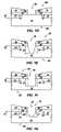
- FIG. 1Ais a sectional view illustrating a semiconductor substrate having an active region and a plurality of discrete conductive elements thereon.
- FIG. 1Bis a plan view of the active surface of a semiconductor substrate illustrating a plurality of semiconductor dice having discrete conductive elements thereon.
- FIGS. 1C-1Gare sectional views illustrating exemplary methods for forming a partial via in a semiconductor substrate that extends from the active surface therein.
- FIGS. 1H-1Jare sectional views illustrating exemplary methods for forming a partial via in a semiconductor substrate that extends from the back surface to form a through via in combination with a partial via extending from the active surface as shown in FIGS. 1C-1G .
- FIGS. 2A-2Care sectional views illustrating yet another exemplary method for forming through vias in a semiconductor substrate.
- the present inventionin a number of embodiments, includes methods for forming through vias that extend through the thickness of a semiconductor substrate between an active surface and a back side thereof without damaging the semiconductor devices formed thereon, and the resulting via structures.
- the present inventionmay be used to form so-called “through wafer interconnects” (TWIs) for electrically connecting the integrated circuitry of semiconductor dice (also encompassed by the term “semiconductor devices” herein) fabricated on the active surface of the semiconductor substrate to another semiconductor device or to higher level packaging.
- TWIsthrough wafer interconnects
- the methods of the present inventionas described in more detail below, may be performed after the semiconductor devices of the semiconductor substrates have been fabricated and tested (e.g., wafer probe burn-in testing).
- FIG. 1Aillustrates a simplified portion of an exemplary semiconductor wafer 8 formed from semiconductor substrate 10 having an active surface 26 and a back surface or back side 28 .
- a semiconductor substrate 10is provided that may have one or more dielectric layers 12 disposed thereon.
- Semiconductor substrate 10may comprise, without limitation, a bulk semiconductor substrate (e.g., a full or partial wafer of semiconductor material, such as silicon, gallium arsenide, indium phosphide, polysilicon, a silicon-on-insulator (SOI) type substrate, such as silicon-on-ceramic (SOC), silicon-on-glass (SOG), or silicon-on-sapphire (SOS), etc.) that includes a plurality of semiconductor devices thereon, and semiconductor dice. If a wafer, semiconductor substrate 10 may also be a full thickness wafer as received from a vendor or a wafer thinned from the back side after fabrication of semiconductor dice thereon.
- a bulk semiconductor substratee.g., a full or partial wafer of semiconductor material, such as silicon, gallium arsenide, indium phosphide, polysilicon
- SOIsilicon-on-insulator
- SOCsilicon-on-ceramic
- SOGsilicon-on-glass
- SOSsilicon-on
- Dielectric layer 12may be formed from materials such as, by way of example only, silicon dioxide, silicon nitride, or borophosphosilicate glass (BPSG).
- Passivation layer 16covers portions of the active surface 26 with discrete conductive elements 14 in the form of bond pads exposed therethrough. Active regions 11 including gate areas or a junction depth 9 and laterally spaced a distance 13 from the periphery of discrete conductive element 14 are illustrated in FIG. 1A .
- the junction depth 9may be, typically, on the order of about 4-5 ⁇ m into the silicon of the semiconductor die, as distinguished from the entire active area or region 11 of the die which includes structures on the surface (not shown) such as transistors, capacitors and other structures, formed as well known in the art.
- Discrete conductive elements 14such as, for example, the aluminum bond pads depicted are shown bonded to the dielectric layer 12 and are electrically connected to the active region 11 using, for example, redistribution lines (RDL) on the active surface 26 that are not shown.
- RDLredistribution lines
- the discrete conductive elements 14are located in portions of “dead space” in the active surface 26 of the semiconductor substrate 10 without integrated circuitry formed thereunder.
- the through vias of the present inventionmay be formed at either the semiconductor die level or at the wafer (or other bulk substrate) level, depending upon the needs of the particular manufacturing process used. While FIG. 1A only shows a single discrete conductive element 14 , it should be understood that semiconductor wafer 8 contains a plurality of discrete conductive elements 14 formed in the “dead space” of a semiconductor substrate 10 between active regions 11 as illustrated in the view of active surface 26 of semiconductor wafer 8 from above as shown in FIG. 1B .
- the reference lines 40define the boundaries or “streets” between individual semiconductor dice 42 formed on the semiconductor wafer 8 .
- an aperture 18may be formed approximately in the center of the discrete conductive elements 14 by appropriately masking and patterning a photoresist or other material (e.g., oxide hard mask) and wet or dry etching.
- a photoresist or other materiale.g., oxide hard mask
- wet or dry etchingemploys a mixture of nitric acid and hydrofluoric (HF) acid in deionized (DI) water. “Dry” etching may also be termed reactive ion etching (RIE).
- RIEreactive ion etching
- either a wet or dry etchantmay be used to form aperture 18 as well as to etch completely through dielectric layer 12 and to remove the native oxide on semiconductor substrate 10 .
- the semiconductor substrate 10is made from silicon, a silicon dioxide native oxide requires removal, and the HF etchant may be used for this purpose prior to etching of the underlying silicon of the semiconductor substrate.
- laser drilling using a plurality, for example two or three, short bursts or pulses from a lasermay be used to remove material from the discrete conductive elements 14 and dielectric layer 12 to form the aperture 18 as shown in FIG. 1D .
- the accurate targeting of the discrete conductive elements 14 with a laser beammay be effected by using fiducial marks on the semiconductor substrate 10 , a machine vision system, or a combination of both. It is currently preferred to use two or three 100-microsecond short bursts from a solid state YAG laser operating at 20 kHz.
- the laser drillingmay be effected using equipment, such as the Model 5000-series lasers, offered currently by ElectroScientific Industries of Portland, OR.
- One specific, suitable piece of equipmentis a 355 nm wavelength UV YAG laser, Model 2700, which may be used to form the aperture 18 .
- Another suitable laser systemis the Xise 200, offered by Xsil Ltd. of Dublin, Ireland, which also has a U.S. office in Loveland, CO.
- the Xsil productmay be used to form vias as little as about 10 ⁇ m to about 15 ⁇ m in diameter.
- the areas of semiconductor substrate 10 irradiated by the lasermay reach a temperature of 1400° C. It is currently believed that above 600° C. damage occurs to the active regions 11 .
- heat flow into the semiconductor substrate 10 due to the thermal input from laseris minimized during forming of aperture 18 and deleterious effects, such as dopant redistribution within the active region 11 , do not occur.
- a wet etchantsuch as a dilute HF etch may be used to remove the native oxide present on the semiconductor substrate 10 .
- wet silicon etchsuch as 6% TMAH in propylene glycol may be used to remove and smooth the heat-damaged silicon surrounding aperture 18 , such heat-damaged silicon being referred to in the art as the heat-affected zone (HAZ).
- partial viasmay be formed within the semiconductor substrate 10 from the active surface thereof by wet etching, dry etching, or laser drilling.
- the partial vias 20 , 20 ′, and 20 ′′ shown in FIGS. 1E-1G , respectively,are formed to extend from the active surface 26 to a depth 21 within the semiconductor substrate 10 .
- a selective wet etchmay be used to form partial via 20 within the semiconductor substrate 10 .
- One suitable selective wet etchantis 6% tetramethyl ammonium hydroxide (TMAH) in propylyene glycol when semiconductor substrate 10 is single crystal silicon.
- This TMAH solutionis a suitable etchant because it will not substantially etch metal or oxide and, thus, will not etch discrete conductive elements 14 . Therefore, it is not necessary to mask the discrete conductive element 14 .
- the TMAHpreferentially etches specific crystal planes of silicon, the (100) and (111) crystal planes, to produce the tapered cross-sectional shape of partial via 20 if the semiconductor substrate 10 is made from single crystal silicon.
- partial via 20 ′may be formed if a dry etchant is used instead of the selective TMAH etchant.
- the partial via 20 ′will exhibit a substantially rectangular (vertical side walls) side cross-sectional configuration in contrast to the tapered cross-section of the partial via 20 formed with the isotropic etchant.
- An anisotropic wet etchantsuch as, for example, 20% to 25% TMAH at 90° C. or 22% KOH at 75° C. may also be used, but an additional silicon oxide or silicon nitride mask layer may then be required to protect the metal of the discrete conductive elements 14 from being etched. If a dry etchant is used, the additional mask layer is not necessary. However, when employing dry etching, the initial mask should be an oxide layer of suitable thickness.
- the partial via 20 ′′may be formed by short burst laser drilling from the active surface in the direction 27 , wherein the partial via 20 ′′ exhibits a larger diameter at the active surface 26 and a smaller diameter at the terminus of the partial via 20 ′′. It should be understood that if the aperture 18 in discrete conductive element 14 is formed using laser drilling, the partial via 20 ′′ may be formed by simply continuing the laser drilling process for a sufficient time to form the partial via 20 ′, taking into account the need to control excessive heating of the semiconductor substrate 10 . At the conclusion of the formation of partial via 20 ′′ using laser drilling, the above described 6% TMAH in propylene glycol may be used to clean and enlarge the partial via, if desired.
- the depth 21 of partial vias 20 , 20 ′, and 20 ′′may be selected to be as deep as junction depth 9 of the associated active regions 11 , which may be, for example, about 4 ⁇ m.
- the depth 21 of partial vias 20 , 20 ′, and 20 ′′may extend sufficiently below the junction depth 9 of active regions 11 so that upon laser drilling from the back surface 28 of semiconductor substrate 10 , the 3-D heat flow from the laser drilling process does not raise the temperature to a sufficient degree to damage the active regions 11 .
- deleterious problemssuch as dopant redistribution within the active region 11 , are not caused by the laser drilling process employed in the present invention. It is currently believed by the inventors that below 600° C.
- An exemplary depth 21 for partial vias 20 , 20 ′, and 20 ′′may be about 5 ⁇ m to about 20 ⁇ m from the active surface 26 .
- a more preferred depth 21 for partial vias 20 , 20 ′, and 20 ′′is about 5 ⁇ m to about 10 ⁇ m from the active surface 26 .
- the precise magnitude for depth 21is dependent on the junction depth 9 of the active regions 11 and the lateral spacing distance 13 of the active regions 11 from the discrete conductive elements 14 . The greater the laterally spacing 13 of the active regions 11 from the discrete conductive elements 14 , the lesser the required depth 21 of the partial vias 20 , 20 ′, and 20 ′′ to avoid damage to active regions 11 .
- the heat flow near a partial via 20 , 20 ′ or 20 ′′ created during the laser drilling processmay not project laterally sufficiently far from the via being formed to raise the temperature within an adjacent active region 11 to a degree to cause substantial dopant redistribution within the active region 11 .
- the integrated circuitry within the active region 11will not degrade or malfunction upon completing a through via by laser drilling from the back surface 28 .
- the through vias 30 of the present inventionmay be completed by laser drilling from the back surface 28 in the direction 38 to form partial via 24 .
- a 355 nm wavelength laseras previously referenced, may be operated at a power of about 4 to 9 W, for example 5 W, and from about a 20 kHz to a 60 kHz cycle or repetition rate to form partial via 24 .
- one partial via 24is partially formed by laser drilling a small amount of material from the back surface 28 of the semiconductor substrate 10 followed by moving to another location and removing a small amount of material from the back surface 28 to partially form another partial via 24 .
- This processis repeated by alternating applications of pulses of laser energy between intended locations of partial vias 24 until a through via 30 is formed in each respective location.
- This alternating processprevents the detrimental buildup of heat in the areas surrounding the partial vias 24 being formed sufficient to damage the active regions 11 .
- the inventorshave found that alternating the application of laser energy between selected locations on the semiconductor substrate 10 enables forming the partial vias 24 at a faster rate than may be accomplished by completely forming a partial via 24 one at a time by the use of multiple sequential pulses applied at a single location. For example, employing the described alternating location process enables forming about 22,000 partial vias 24 in about ten minutes.
- the depth of substrate material drilled by the lasermay be controlled based on an experimental correlation between the number of pulses and the amount of material ablated from semiconductor substrate 10 .
- the laser drilling processremoves the remaining material from semiconductor substrate 10 between the back surface 28 and the bottom of a partial via 20 , 20 ′ or 20 ′′ necessary to form a through via 30 that extends from the back surface 28 to the active surface 26 .
- an isotropic wet etchantsuch as a 6% TMAH in propylene glycol, may be used to remove any debris caused by the laser drilling process, to remove the heat-damaged material commonly termed the heat affected zone, or HAZ, present at the interior walls of the partial via 24 due to the laser drilling process, to smooth the interior region of the through via 30 , and to enlarge the diameter of the through via 30 .
- FIGS. 1H-1JThe resultant side cross-sectional shapes for the through vias 30 formed using the various processes are illustrated in FIGS. 1H-1J .
- FIG. 1Hillustrates through via 30 when the partial via 20 is formed using an anisotropic etchant.
- FIG. 1Iillustrates the cross-sectional shape of through via 30 when an isotropic etchant or a dry etchant is used to form the partial via 20 ′.
- FIG. 1Jillustrates the cross-sectional shape of through via 30 when the partial via 20 ′′ is formed using laser drilling.
- the diametertypically, is larger at the back surface 28 , tapering down to a smaller diameter where the partial via 24 terminates at the bottom of a partial via 20 , 20 ′ or 20 ′′.
- the through vias 30may also, in accordance with the present invention, be formed by first laser drilling from the back surface 28 in a direction 38 to form partial via 24 followed by forming the aperture 18 and subsequently a partial via 20 , 20 ′ or 20 ′′ as previously described to effect removal of material from the active surface 26 in a direction toward the back surface 28 until partial via 24 is intersected.
- FIGS. 2A-2CAnother exemplary method for forming through vias 30 is described with respect to FIGS. 2A-2C .
- the exemplary method illustrated in FIGS. 2A-2Cenables rapidly forming a majority of a through via using laser drilling.
- the remainder of the through via proximate the active regions 11may be formed by a process that does not create a heat flow that damages the integrated circuitry within the active region 11 .
- a semiconductor wafer 8is provided that is identical to that described in FIG. 1A .
- a partial via 34 having a depth 32 from the back surface 28may be formed by laser drilling from the back surface 28 of the semiconductor substrate 10 in a direction 38 toward active surface 28 to effect the removal of material from semiconductor substrate 10 .
- a 355 nm wavelength laser operated, for example, power of 5 Wmay effect a nominal 3 ⁇ m depth ablation per pulse through the silicon.
- a range of power from the aforementioned 4 W to 9 W and a pulse or repetition rate of about 20 to about 60 kHzmay be suitable, the number of pulses required to reach a desired depth being determinable from an initial via cross-section ablated by the laser beam.
- the partial via 34may be formed to terminate approximately 25 ⁇ m or more from the active regions 11 , as shown by distance 35 in FIG. 2B . However, the depth 32 of the partial via 34 may extend from the back surface 28 and terminate at junction depth 9 of the active regions 11 . As with the exemplary embodiments illustrated in FIGS.
- the precise magnitude for depth 32 of partial via 34is dependent on the junction depth 9 of the active regions 11 and the lateral spacing distance 13 of the active regions 11 from the paths and side wall locations of the through vias to be formed.
- one partial via 34may be partially formed by laser drilling a small amount of material from the back surface 28 of the semiconductor substrate 10 followed by moving to another location and removing a small amount of material from the back surface 28 to partially form another partial via 34 . This process is repeated by alternating laser drilling between partially formed partial vias 34 until each respective partial via 34 has been formed to its desired depth 32 .
- the remaining semiconductor substrate 10 and dielectric layer 12 between the end of the partial via 34 most proximate active surface 26 and the discrete conductive element 14may be removed to form the complete through via 30 by employing a dry etching technique, such as the aforementioned reactive ion etching (RIE).
- RIEreactive ion etching
- One suitable reactive ion etching process that may be employed to form the partial via 34is a deep reactive ion etch known as the “Bosch Process,” wherein the semiconductor substrate is alternately exposed to an etchant plasma and a passivant plasma.
- the via side wall profile formedis substantially vertical, the side walls exhibit a “scalloped” texture due to the alternating etching and passivating sequence, and the etch rate, profile and selectivity to a mask material used to cover the back surface 28 of the semiconductor substrate 10 may be controlled by adjusting etch and passivation step efficiency or the time ratio of exposure of the semiconductor substrate 10 to the two types of steps.
- the plasma etchant employedis SF 6 and the passivant is C 4 F 8 .
- Suitable equipment for effecting the deep silicon etch processis available from Oxford Instruments Plasma Technology of Fremont, CA.
- the dry etching processeffects removal of the remaining semiconductor substrate 10 and dielectric layer 12 between the bottom or end of the partial via 34 and the discrete conductive element 14 in the direction 38 to form the partial via 36 .
- Partial via 36exhibits a substantially rectangular cross-section having substantially vertical side walls 39 .
- the dry etching processexposes a back side of the discrete conductive elements 14 and forms partial via 36 having a smaller diameter than partial via 34 .
- the dry etchingis used to form the partial via 36 because of the proximity of partial via 36 to the active region 11 .
- the dry etching processdoes not create any heat flow projecting from the partial via 36 during its formation capable of causing dopant redistribution within the active region 11 .
- dry etching alonewas used to form the through vias 30 , the required time to form the through vias 30 would be too long and the process too expensive.
- the through via 30would extend through the discrete conductive element 14 due to difficulty in controlling the depth of the via formed with the laser.
- the above methodemploys laser drilling to rapidly form the majority of the through via 30 , while the much slower dry etching process is reserved for forming the portion of through via 30 proximate the sensitive active regions 11 .
- an isotropic etchantsuch as 6% TMAH in propylene glycol, may be used to remove any debris caused by the laser drilling process, to remove the heat affected material (HAZ) present proximate the interior walls of the partial via 34 due to the laser drilling process, to smooth the interior region of the through via 30 , and to enlarge the diameter of the through via 30 .
- a conductive filler material(not shown) may be used to fill the through vias to form TWIs having a conductive pathway with the external conductive element 14 .
- a conductive filler materialsuch as a metal or alloy
- PVDphysical vapor deposition
- a solder pastemay also be placed in through vias 30 , and reflowed.
- a conductive or conductor-filled epoxymay be used.
- the side walls of through vias 30must be coated with a layer of dielectric material to avoid short-circuiting of the conductive filler to the silicon of the substrate.
- the dielectric material layermay comprise spin-on-glass, thermal oxide, PARYLENETM polymer, low silane oxide (LSO), a pulse deposition layer comprising aluminum rich oxide, silicon dioxide, silicon nitride, silicon oxynitride, a glass, i.e., borophosphosilicate glass, phosphosilicate glass, borosilicate glass, or any other dielectric material having a low dielectric constant known in the art.
- LSOlow silane oxide
- a redistribution layercomprising traces and, optionally associated discrete external conductive elements thereon such as solder bumps may be formed on the back surface 28 and electrically interconnected with the TWIs, as is known in the art, for example by forming the traces over the conductive filler material at the back surface ends of the through vias 30 .
Landscapes
- Engineering & Computer Science (AREA)
- Physics & Mathematics (AREA)
- Condensed Matter Physics & Semiconductors (AREA)
- General Physics & Mathematics (AREA)
- Manufacturing & Machinery (AREA)
- Computer Hardware Design (AREA)
- Microelectronics & Electronic Packaging (AREA)
- Power Engineering (AREA)
- Internal Circuitry In Semiconductor Integrated Circuit Devices (AREA)
Abstract
Description
Claims (29)
Priority Applications (3)
| Application Number | Priority Date | Filing Date | Title |
|---|---|---|---|
| US11/140,402US7598167B2 (en) | 2004-08-24 | 2005-05-27 | Method of forming vias in semiconductor substrates without damaging active regions thereof and resulting structures |
| US11/781,083US7855140B2 (en) | 2004-08-24 | 2007-07-20 | Method of forming vias in semiconductor substrates and resulting structures |
| US12/955,359US8786097B2 (en) | 2004-08-24 | 2010-11-29 | Method of forming vias in semiconductor substrates and resulting structures |
Applications Claiming Priority (2)
| Application Number | Priority Date | Filing Date | Title |
|---|---|---|---|
| US60423404P | 2004-08-24 | 2004-08-24 | |
| US11/140,402US7598167B2 (en) | 2004-08-24 | 2005-05-27 | Method of forming vias in semiconductor substrates without damaging active regions thereof and resulting structures |
Related Child Applications (1)
| Application Number | Title | Priority Date | Filing Date |
|---|---|---|---|
| US11/781,083ContinuationUS7855140B2 (en) | 2004-08-24 | 2007-07-20 | Method of forming vias in semiconductor substrates and resulting structures |
Publications (2)
| Publication Number | Publication Date |
|---|---|
| US20060046463A1 US20060046463A1 (en) | 2006-03-02 |
| US7598167B2true US7598167B2 (en) | 2009-10-06 |
Family
ID=35943890
Family Applications (3)
| Application Number | Title | Priority Date | Filing Date |
|---|---|---|---|
| US11/140,402Active2027-08-02US7598167B2 (en) | 2004-08-24 | 2005-05-27 | Method of forming vias in semiconductor substrates without damaging active regions thereof and resulting structures |
| US11/781,083Active2026-11-26US7855140B2 (en) | 2004-08-24 | 2007-07-20 | Method of forming vias in semiconductor substrates and resulting structures |
| US12/955,359Expired - LifetimeUS8786097B2 (en) | 2004-08-24 | 2010-11-29 | Method of forming vias in semiconductor substrates and resulting structures |
Family Applications After (2)
| Application Number | Title | Priority Date | Filing Date |
|---|---|---|---|
| US11/781,083Active2026-11-26US7855140B2 (en) | 2004-08-24 | 2007-07-20 | Method of forming vias in semiconductor substrates and resulting structures |
| US12/955,359Expired - LifetimeUS8786097B2 (en) | 2004-08-24 | 2010-11-29 | Method of forming vias in semiconductor substrates and resulting structures |
Country Status (1)
| Country | Link |
|---|---|
| US (3) | US7598167B2 (en) |
Cited By (11)
| Publication number | Priority date | Publication date | Assignee | Title |
|---|---|---|---|---|
| US20070262464A1 (en)* | 2004-08-24 | 2007-11-15 | Micron Technology, Inc. | Method of forming vias in semiconductor substrates and resulting structures |
| US20080179756A1 (en)* | 2007-01-31 | 2008-07-31 | Kamins Theodore I | Semiconductor structures including conductive vias and methods of making semiconductor structures |
| US20140084474A1 (en)* | 2011-05-23 | 2014-03-27 | Dominique SUHR | Method for forming a vertical electrical connection in a layered semiconductor structure |
| US8894868B2 (en) | 2011-10-06 | 2014-11-25 | Electro Scientific Industries, Inc. | Substrate containing aperture and methods of forming the same |
| US20150233008A1 (en)* | 2014-02-13 | 2015-08-20 | Skyworks Solutions, Inc. | Apparatus and methods related to copper plating of wafers |
| WO2017023677A1 (en) | 2015-08-03 | 2017-02-09 | Fujifilm Electronic Materials U.S.A., Inc. | Cleaning composition |
| WO2018232214A1 (en) | 2017-06-16 | 2018-12-20 | Fujifilm Electronic Materials U.S.A., Inc. | Multilayer structure |
| WO2019050566A1 (en) | 2017-09-11 | 2019-03-14 | Fujifilm Electronic Materials U.S.A., Inc. | Dielectric film forming composition |
| US20200118826A1 (en)* | 2018-10-16 | 2020-04-16 | Cerebras Systems Inc. | Systems and methods for precision fabrication of an orifice within an integrated circuit |
| US11145530B2 (en) | 2019-11-08 | 2021-10-12 | Cerebras Systems Inc. | System and method for alignment of an integrated circuit |
| US20220059515A1 (en)* | 2016-11-28 | 2022-02-24 | Taiwan Semiconductor Manufacturing Co., Ltd. | Method of forming package structure |
Families Citing this family (56)
| Publication number | Priority date | Publication date | Assignee | Title |
|---|---|---|---|---|
| US9985207B2 (en)* | 2004-12-06 | 2018-05-29 | Flexenable Limited | Electronic devices |
| US20070007621A1 (en)* | 2005-03-30 | 2007-01-11 | Yamaha Corporation | Fuse breakdown method adapted to semiconductor device |
| JP2007067082A (en)* | 2005-08-30 | 2007-03-15 | Disco Abrasive Syst Ltd | Wafer drilling method |
| US8212331B1 (en)* | 2006-10-02 | 2012-07-03 | Newport Fab, Llc | Method for fabricating a backside through-wafer via in a processed wafer and related structure |
| US7791199B2 (en) | 2006-11-22 | 2010-09-07 | Tessera, Inc. | Packaged semiconductor chips |
| US8569876B2 (en) | 2006-11-22 | 2013-10-29 | Tessera, Inc. | Packaged semiconductor chips with array |
| JP2008155274A (en)* | 2006-12-26 | 2008-07-10 | Disco Abrasive Syst Ltd | Wafer processing method |
| JP4314278B2 (en)* | 2007-01-22 | 2009-08-12 | エルピーダメモリ株式会社 | Semiconductor device and manufacturing method thereof |
| US8405196B2 (en)* | 2007-03-05 | 2013-03-26 | DigitalOptics Corporation Europe Limited | Chips having rear contacts connected by through vias to front contacts |
| JP4380718B2 (en) | 2007-03-15 | 2009-12-09 | ソニー株式会社 | Manufacturing method of semiconductor device |
| JP2008288285A (en)* | 2007-05-15 | 2008-11-27 | Sharp Corp | LAMINATED SUBSTRATE CUTTING METHOD, SEMICONDUCTOR DEVICE MANUFACTURING METHOD, SEMICONDUCTOR DEVICE, LIGHT EMITTING DEVICE, AND BACKLIGHT DEVICE |
| US7564115B2 (en)* | 2007-05-16 | 2009-07-21 | Taiwan Semiconductor Manufacturing Company, Ltd. | Tapered through-silicon via structure |
| GB2451909B (en) | 2007-08-17 | 2012-07-11 | Wolfson Microelectronics Plc | Mems process and device |
| WO2009017835A2 (en) | 2007-07-31 | 2009-02-05 | Tessera, Inc. | Semiconductor packaging process using through silicon vias |
| JP5656341B2 (en)* | 2007-10-29 | 2015-01-21 | ピーエスフォー ルクスコ エスエイアールエルPS4 Luxco S.a.r.l. | Semiconductor device and manufacturing method thereof |
| US8912654B2 (en)* | 2008-04-11 | 2014-12-16 | Qimonda Ag | Semiconductor chip with integrated via |
| US7666711B2 (en)* | 2008-05-27 | 2010-02-23 | Stats Chippac, Ltd. | Semiconductor device and method of forming double-sided through vias in saw streets |
| US8257603B2 (en)* | 2008-08-29 | 2012-09-04 | Corning Incorporated | Laser patterning of glass bodies |
| US8048689B2 (en)* | 2008-09-25 | 2011-11-01 | Globalfoundries Inc. | Semiconductor chip with backside conductor structure |
| WO2010044741A1 (en) | 2008-10-15 | 2010-04-22 | ÅAC Microtec AB | Method for making via interconnection |
| US9346130B2 (en) | 2008-12-17 | 2016-05-24 | Electro Scientific Industries, Inc. | Method for laser processing glass with a chamfered edge |
| US8049327B2 (en)* | 2009-01-05 | 2011-11-01 | Taiwan Semiconductor Manufacturing Company, Ltd. | Through-silicon via with scalloped sidewalls |
| JP5377993B2 (en)* | 2009-01-30 | 2013-12-25 | 株式会社日立ハイテクノロジーズ | Plasma processing method |
| KR20110000960A (en)* | 2009-06-29 | 2011-01-06 | 삼성전자주식회사 | Semiconductor chip, stack module, memory card and manufacturing method thereof |
| US8519538B2 (en)* | 2010-04-28 | 2013-08-27 | Taiwan Semiconductor Manufacturing Company, Ltd. | Laser etch via formation |
| US9640437B2 (en)* | 2010-07-23 | 2017-05-02 | Tessera, Inc. | Methods of forming semiconductor elements using micro-abrasive particle stream |
| US8796135B2 (en) | 2010-07-23 | 2014-08-05 | Tessera, Inc. | Microelectronic elements with rear contacts connected with via first or via middle structures |
| US8791575B2 (en)* | 2010-07-23 | 2014-07-29 | Tessera, Inc. | Microelectronic elements having metallic pads overlying vias |
| US8847380B2 (en) | 2010-09-17 | 2014-09-30 | Tessera, Inc. | Staged via formation from both sides of chip |
| US8610259B2 (en) | 2010-09-17 | 2013-12-17 | Tessera, Inc. | Multi-function and shielded 3D interconnects |
| US8736066B2 (en) | 2010-12-02 | 2014-05-27 | Tessera, Inc. | Stacked microelectronic assemby with TSVS formed in stages and carrier above chip |
| US8637968B2 (en) | 2010-12-02 | 2014-01-28 | Tessera, Inc. | Stacked microelectronic assembly having interposer connecting active chips |
| US8587126B2 (en) | 2010-12-02 | 2013-11-19 | Tessera, Inc. | Stacked microelectronic assembly with TSVs formed in stages with plural active chips |
| US8610264B2 (en) | 2010-12-08 | 2013-12-17 | Tessera, Inc. | Compliant interconnects in wafers |
| US20120168412A1 (en)* | 2011-01-05 | 2012-07-05 | Electro Scientific Industries, Inc | Apparatus and method for forming an aperture in a substrate |
| US9078343B2 (en)* | 2011-02-22 | 2015-07-07 | Ibiden Co., Ltd. | Method for manufacturing printed wiring board |
| US8853072B2 (en) | 2011-06-06 | 2014-10-07 | Micron Technology, Inc. | Methods of forming through-substrate interconnects |
| US9079269B2 (en)* | 2011-11-22 | 2015-07-14 | International Business Machines Corporation | Spalling with laser-defined spall edge regions |
| JP5810921B2 (en)* | 2012-01-06 | 2015-11-11 | 凸版印刷株式会社 | Manufacturing method of semiconductor device |
| US10357850B2 (en) | 2012-09-24 | 2019-07-23 | Electro Scientific Industries, Inc. | Method and apparatus for machining a workpiece |
| US9828278B2 (en) | 2012-02-28 | 2017-11-28 | Electro Scientific Industries, Inc. | Method and apparatus for separation of strengthened glass and articles produced thereby |
| KR20140138134A (en) | 2012-02-28 | 2014-12-03 | 일렉트로 싸이언티픽 인더스트리이즈 인코포레이티드 | Method and apparatus for separation of strengthened glass and articles produced thereby |
| WO2013130608A1 (en) | 2012-02-29 | 2013-09-06 | Electro Scientific Industries, Inc. | Methods and apparatus for machining strengthened glass and articles produced thereby |
| US8519516B1 (en) | 2012-03-12 | 2013-08-27 | Micron Technology, Inc. | Semiconductor constructions |
| DE112014001285T5 (en)* | 2013-03-14 | 2015-12-03 | Ps4 Luxco S.A.R.L. | Semiconductor chip and semiconductor device, which is provided with the semiconductor chip |
| CN107658284B (en)* | 2013-10-25 | 2020-07-14 | 日月光半导体制造股份有限公司 | Semiconductor package and method of manufacturing the same |
| US20150263056A1 (en)* | 2014-03-12 | 2015-09-17 | Aeroflex Colorado Springs Inc. | Structures and methods of forming photodiode arrays having through-semiconductor vias |
| US9776906B2 (en) | 2014-03-28 | 2017-10-03 | Electro Scientific Industries, Inc. | Laser machining strengthened glass |
| KR102117471B1 (en)* | 2015-01-12 | 2020-06-01 | 삼성전기주식회사 | Acoustic resonator and manufacturing method thereof |
| US10442720B2 (en)* | 2015-10-01 | 2019-10-15 | AGC Inc. | Method of forming hole in glass substrate by using pulsed laser, and method of producing glass substrate provided with hole |
| US9847290B1 (en)* | 2016-12-12 | 2017-12-19 | Globalfoundries Inc. | Through-silicon via with improved substrate contact for reduced through-silicon via (TSV) capacitance variability |
| US11652036B2 (en)* | 2018-04-02 | 2023-05-16 | Santa Clara | Via-trace structures |
| CN114556555A (en)* | 2019-09-13 | 2022-05-27 | 康宁公司 | System and method for reducing the impact of via formation on electronic device formation |
| US11817304B2 (en)* | 2019-12-30 | 2023-11-14 | Micron Technology, Inc. | Method of manufacturing microelectronic devices, related devices, systems, and apparatus |
| US11289404B2 (en) | 2020-01-17 | 2022-03-29 | Taiwan Semiconductor Manufacturing Company, Ltd. | Semiconductor device and method |
| JP7493667B2 (en)* | 2021-02-17 | 2024-05-31 | 三菱電機株式会社 | NITRIDE SEMICONDUCTOR DEVICE AND METHOD FOR MANUFACTURING NITRIDE SEMICON |
Citations (12)
| Publication number | Priority date | Publication date | Assignee | Title |
|---|---|---|---|---|
| US4445978A (en) | 1983-03-09 | 1984-05-01 | Rca Corporation | Method for fabricating via connectors through semiconductor wafers |
| US4806111A (en) | 1985-11-01 | 1989-02-21 | Hitachi, Ltd. | Connector structure |
| US5229647A (en) | 1991-03-27 | 1993-07-20 | Micron Technology, Inc. | High density data storage using stacked wafers |
| US5438212A (en) | 1993-02-25 | 1995-08-01 | Mitsubishi Denki Kabushiki Kaisha | Semiconductor device with heat dissipation structure |
| US6013948A (en) | 1995-11-27 | 2000-01-11 | Micron Technology, Inc. | Stackable chip scale semiconductor package with mating contacts on opposed surfaces |
| US6018196A (en) | 1996-11-08 | 2000-01-25 | W. L. Gore & Associates, Inc. | Semiconductor flip chip package |
| US6114240A (en) | 1997-12-18 | 2000-09-05 | Micron Technology, Inc. | Method for fabricating semiconductor components using focused laser beam |
| US6294425B1 (en)* | 1999-10-14 | 2001-09-25 | Samsung Electronics Co., Ltd. | Methods of forming integrated circuit capacitors by electroplating electrodes from seed layers |
| US6420209B1 (en) | 1996-10-29 | 2002-07-16 | Tru-Si Technologies, Inc. | Integrated circuits and methods for their fabrication |
| US6620731B1 (en) | 1997-12-18 | 2003-09-16 | Micron Technology, Inc. | Method for fabricating semiconductor components and interconnects with contacts on opposing sides |
| US6667551B2 (en)* | 2000-01-21 | 2003-12-23 | Seiko Epson Corporation | Semiconductor device and manufacturing thereof, including a through-hole with a wider intermediate cavity |
| US20070262464A1 (en)* | 2004-08-24 | 2007-11-15 | Micron Technology, Inc. | Method of forming vias in semiconductor substrates and resulting structures |
Family Cites Families (1)
| Publication number | Priority date | Publication date | Assignee | Title |
|---|---|---|---|---|
| US4445987A (en)* | 1983-03-30 | 1984-05-01 | Oronzio De Nora S.A. | Electrolytic purification and reconcentration of wash and rinse caustic solutions recovered from the regeneration of ion exchange resins |
- 2005
- 2005-05-27USUS11/140,402patent/US7598167B2/enactiveActive
- 2007
- 2007-07-20USUS11/781,083patent/US7855140B2/enactiveActive
- 2010
- 2010-11-29USUS12/955,359patent/US8786097B2/ennot_activeExpired - Lifetime
Patent Citations (12)
| Publication number | Priority date | Publication date | Assignee | Title |
|---|---|---|---|---|
| US4445978A (en) | 1983-03-09 | 1984-05-01 | Rca Corporation | Method for fabricating via connectors through semiconductor wafers |
| US4806111A (en) | 1985-11-01 | 1989-02-21 | Hitachi, Ltd. | Connector structure |
| US5229647A (en) | 1991-03-27 | 1993-07-20 | Micron Technology, Inc. | High density data storage using stacked wafers |
| US5438212A (en) | 1993-02-25 | 1995-08-01 | Mitsubishi Denki Kabushiki Kaisha | Semiconductor device with heat dissipation structure |
| US6013948A (en) | 1995-11-27 | 2000-01-11 | Micron Technology, Inc. | Stackable chip scale semiconductor package with mating contacts on opposed surfaces |
| US6420209B1 (en) | 1996-10-29 | 2002-07-16 | Tru-Si Technologies, Inc. | Integrated circuits and methods for their fabrication |
| US6018196A (en) | 1996-11-08 | 2000-01-25 | W. L. Gore & Associates, Inc. | Semiconductor flip chip package |
| US6114240A (en) | 1997-12-18 | 2000-09-05 | Micron Technology, Inc. | Method for fabricating semiconductor components using focused laser beam |
| US6620731B1 (en) | 1997-12-18 | 2003-09-16 | Micron Technology, Inc. | Method for fabricating semiconductor components and interconnects with contacts on opposing sides |
| US6294425B1 (en)* | 1999-10-14 | 2001-09-25 | Samsung Electronics Co., Ltd. | Methods of forming integrated circuit capacitors by electroplating electrodes from seed layers |
| US6667551B2 (en)* | 2000-01-21 | 2003-12-23 | Seiko Epson Corporation | Semiconductor device and manufacturing thereof, including a through-hole with a wider intermediate cavity |
| US20070262464A1 (en)* | 2004-08-24 | 2007-11-15 | Micron Technology, Inc. | Method of forming vias in semiconductor substrates and resulting structures |
Non-Patent Citations (2)
| Title |
|---|
| Chu et al., Laser Micromachining of Through Via Interconnects in Active Die for 3-D Multichip Module, IEEE/CMPT Int'l EMT Symposium, 1995, pp. 120-126. |
| Lee et al., Laser Created Silicon Vias for Stacking Dies in MCMs, EMT Symposium, 1991, Tampa, Florida, pp. 262-265. |
Cited By (20)
| Publication number | Priority date | Publication date | Assignee | Title |
|---|---|---|---|---|
| US20070262464A1 (en)* | 2004-08-24 | 2007-11-15 | Micron Technology, Inc. | Method of forming vias in semiconductor substrates and resulting structures |
| US7855140B2 (en)* | 2004-08-24 | 2010-12-21 | Micron Technology, Inc. | Method of forming vias in semiconductor substrates and resulting structures |
| US20110074043A1 (en)* | 2004-08-24 | 2011-03-31 | Micron Technology, Inc. | Method of forming vias in semiconductor substrates and resulting structures |
| US8786097B2 (en) | 2004-08-24 | 2014-07-22 | Micron Technology, Inc. | Method of forming vias in semiconductor substrates and resulting structures |
| US20080179756A1 (en)* | 2007-01-31 | 2008-07-31 | Kamins Theodore I | Semiconductor structures including conductive vias and methods of making semiconductor structures |
| US7804175B2 (en)* | 2007-01-31 | 2010-09-28 | Hewlett-Packard Development Company, L.P. | Semiconductor structures including conductive vias continuously extending therethrough and methods of making the same |
| US20140084474A1 (en)* | 2011-05-23 | 2014-03-27 | Dominique SUHR | Method for forming a vertical electrical connection in a layered semiconductor structure |
| US9368397B2 (en)* | 2011-05-23 | 2016-06-14 | Alchimer | Method for forming a vertical electrical connection in a layered semiconductor structure |
| US8894868B2 (en) | 2011-10-06 | 2014-11-25 | Electro Scientific Industries, Inc. | Substrate containing aperture and methods of forming the same |
| US20150233008A1 (en)* | 2014-02-13 | 2015-08-20 | Skyworks Solutions, Inc. | Apparatus and methods related to copper plating of wafers |
| WO2017023677A1 (en) | 2015-08-03 | 2017-02-09 | Fujifilm Electronic Materials U.S.A., Inc. | Cleaning composition |
| US20220059515A1 (en)* | 2016-11-28 | 2022-02-24 | Taiwan Semiconductor Manufacturing Co., Ltd. | Method of forming package structure |
| US11817437B2 (en)* | 2016-11-28 | 2023-11-14 | Taiwan Semiconductor Manufacturing Co., Ltd. | Method of forming package structure |
| US12191287B2 (en) | 2016-11-28 | 2025-01-07 | Taiwan Semiconductor Manufacturing Co., Ltd. | Package structure |
| WO2018232214A1 (en) | 2017-06-16 | 2018-12-20 | Fujifilm Electronic Materials U.S.A., Inc. | Multilayer structure |
| WO2019050566A1 (en) | 2017-09-11 | 2019-03-14 | Fujifilm Electronic Materials U.S.A., Inc. | Dielectric film forming composition |
| US20200118826A1 (en)* | 2018-10-16 | 2020-04-16 | Cerebras Systems Inc. | Systems and methods for precision fabrication of an orifice within an integrated circuit |
| US10957595B2 (en) | 2018-10-16 | 2021-03-23 | Cerebras Systems Inc. | Systems and methods for precision fabrication of an orifice within an integrated circuit |
| US10971401B2 (en)* | 2018-10-16 | 2021-04-06 | Cerebras Systems Inc. | Systems and methods for precision fabrication of an orifice within an integrated circuit |
| US11145530B2 (en) | 2019-11-08 | 2021-10-12 | Cerebras Systems Inc. | System and method for alignment of an integrated circuit |
Also Published As
| Publication number | Publication date |
|---|---|
| US8786097B2 (en) | 2014-07-22 |
| US20110074043A1 (en) | 2011-03-31 |
| US7855140B2 (en) | 2010-12-21 |
| US20070262464A1 (en) | 2007-11-15 |
| US20060046463A1 (en) | 2006-03-02 |
Similar Documents
| Publication | Publication Date | Title |
|---|---|---|
| US7598167B2 (en) | Method of forming vias in semiconductor substrates without damaging active regions thereof and resulting structures | |
| US10886232B2 (en) | Package structure and fabrication methods | |
| US8558351B2 (en) | Alignment for backside illumination sensor | |
| US8198734B2 (en) | Silicon-on-insulator structures for through via in silicon carriers | |
| US8329578B2 (en) | Via structure and via etching process of forming the same | |
| US8268723B2 (en) | Methods for forming semiconductor device structures | |
| KR102436170B1 (en) | Wafer bonding method | |
| CN104658969B (en) | The autoregistration of redistribution layer | |
| US20060270196A1 (en) | Methods of forming semiconductor devices and electrical interconnect structures in semiconductor devices and intermediate structures formed thereby | |
| KR101720406B1 (en) | Semiconductor device and fabricating method thereof | |
| KR20240089267A (en) | Substrate structuring methods | |
| US12015008B2 (en) | Wafer bonding method | |
| TWI765524B (en) | Semiconductor device and the method for forming the same | |
| JP2018032757A (en) | Semiconductor device and manufacturing method for the same | |
| JP4285604B2 (en) | Substrate with through electrode, method for manufacturing the same, and electronic device | |
| JP3698160B2 (en) | Manufacturing method of semiconductor device | |
| TW202221810A (en) | Methods of tsv formation for advanced packaging | |
| JP4019985B2 (en) | Semiconductor device manufacturing method, circuit board, and electronic apparatus | |
| TW202404893A (en) | Mems device and method forming the same | |
| CN117088329A (en) | Semiconductor structure and forming method thereof |
Legal Events
| Date | Code | Title | Description |
|---|---|---|---|
| AS | Assignment | Owner name:MICRON TECHNOLOGY, INC., IDAHO Free format text:ASSIGNMENT OF ASSIGNORS INTEREST;ASSIGNORS:WATKINS, CHARLES M.;KIRBY, KYLE K.;WOOD, ALAN G.;AND OTHERS;REEL/FRAME:016647/0168 Effective date:20050429 | |
| FEPP | Fee payment procedure | Free format text:PAYOR NUMBER ASSIGNED (ORIGINAL EVENT CODE: ASPN); ENTITY STATUS OF PATENT OWNER: LARGE ENTITY | |
| STCF | Information on status: patent grant | Free format text:PATENTED CASE | |
| CC | Certificate of correction | ||
| FPAY | Fee payment | Year of fee payment:4 | |
| AS | Assignment | Owner name:U.S. BANK NATIONAL ASSOCIATION, AS COLLATERAL AGENT, CALIFORNIA Free format text:SECURITY INTEREST;ASSIGNOR:MICRON TECHNOLOGY, INC.;REEL/FRAME:038669/0001 Effective date:20160426 Owner name:U.S. BANK NATIONAL ASSOCIATION, AS COLLATERAL AGEN Free format text:SECURITY INTEREST;ASSIGNOR:MICRON TECHNOLOGY, INC.;REEL/FRAME:038669/0001 Effective date:20160426 | |
| AS | Assignment | Owner name:MORGAN STANLEY SENIOR FUNDING, INC., AS COLLATERAL AGENT, MARYLAND Free format text:PATENT SECURITY AGREEMENT;ASSIGNOR:MICRON TECHNOLOGY, INC.;REEL/FRAME:038954/0001 Effective date:20160426 Owner name:MORGAN STANLEY SENIOR FUNDING, INC., AS COLLATERAL Free format text:PATENT SECURITY AGREEMENT;ASSIGNOR:MICRON TECHNOLOGY, INC.;REEL/FRAME:038954/0001 Effective date:20160426 | |
| FPAY | Fee payment | Year of fee payment:8 | |
| AS | Assignment | Owner name:U.S. BANK NATIONAL ASSOCIATION, AS COLLATERAL AGENT, CALIFORNIA Free format text:CORRECTIVE ASSIGNMENT TO CORRECT THE REPLACE ERRONEOUSLY FILED PATENT #7358718 WITH THE CORRECT PATENT #7358178 PREVIOUSLY RECORDED ON REEL 038669 FRAME 0001. ASSIGNOR(S) HEREBY CONFIRMS THE SECURITY INTEREST;ASSIGNOR:MICRON TECHNOLOGY, INC.;REEL/FRAME:043079/0001 Effective date:20160426 Owner name:U.S. BANK NATIONAL ASSOCIATION, AS COLLATERAL AGEN Free format text:CORRECTIVE ASSIGNMENT TO CORRECT THE REPLACE ERRONEOUSLY FILED PATENT #7358718 WITH THE CORRECT PATENT #7358178 PREVIOUSLY RECORDED ON REEL 038669 FRAME 0001. ASSIGNOR(S) HEREBY CONFIRMS THE SECURITY INTEREST;ASSIGNOR:MICRON TECHNOLOGY, INC.;REEL/FRAME:043079/0001 Effective date:20160426 | |
| AS | Assignment | Owner name:JPMORGAN CHASE BANK, N.A., AS COLLATERAL AGENT, ILLINOIS Free format text:SECURITY INTEREST;ASSIGNORS:MICRON TECHNOLOGY, INC.;MICRON SEMICONDUCTOR PRODUCTS, INC.;REEL/FRAME:047540/0001 Effective date:20180703 Owner name:JPMORGAN CHASE BANK, N.A., AS COLLATERAL AGENT, IL Free format text:SECURITY INTEREST;ASSIGNORS:MICRON TECHNOLOGY, INC.;MICRON SEMICONDUCTOR PRODUCTS, INC.;REEL/FRAME:047540/0001 Effective date:20180703 | |
| AS | Assignment | Owner name:MICRON TECHNOLOGY, INC., IDAHO Free format text:RELEASE BY SECURED PARTY;ASSIGNOR:U.S. BANK NATIONAL ASSOCIATION, AS COLLATERAL AGENT;REEL/FRAME:047243/0001 Effective date:20180629 | |
| AS | Assignment | Owner name:MICRON TECHNOLOGY, INC., IDAHO Free format text:RELEASE BY SECURED PARTY;ASSIGNOR:MORGAN STANLEY SENIOR FUNDING, INC., AS COLLATERAL AGENT;REEL/FRAME:050937/0001 Effective date:20190731 | |
| AS | Assignment | Owner name:MICRON TECHNOLOGY, INC., IDAHO Free format text:RELEASE BY SECURED PARTY;ASSIGNOR:JPMORGAN CHASE BANK, N.A., AS COLLATERAL AGENT;REEL/FRAME:051028/0001 Effective date:20190731 Owner name:MICRON SEMICONDUCTOR PRODUCTS, INC., IDAHO Free format text:RELEASE BY SECURED PARTY;ASSIGNOR:JPMORGAN CHASE BANK, N.A., AS COLLATERAL AGENT;REEL/FRAME:051028/0001 Effective date:20190731 | |
| MAFP | Maintenance fee payment | Free format text:PAYMENT OF MAINTENANCE FEE, 12TH YEAR, LARGE ENTITY (ORIGINAL EVENT CODE: M1553); ENTITY STATUS OF PATENT OWNER: LARGE ENTITY Year of fee payment:12 |