US7597561B2 - Method and system for batch forming spring elements in three dimensions - Google Patents
Method and system for batch forming spring elements in three dimensionsDownload PDFInfo
- Publication number
- US7597561B2 US7597561B2US11/083,031US8303105AUS7597561B2US 7597561 B2US7597561 B2US 7597561B2US 8303105 AUS8303105 AUS 8303105AUS 7597561 B2US7597561 B2US 7597561B2
- Authority
- US
- United States
- Prior art keywords
- contact
- die
- spring
- sheet
- spacer layer
- Prior art date
- Legal status (The legal status is an assumption and is not a legal conclusion. Google has not performed a legal analysis and makes no representation as to the accuracy of the status listed.)
- Expired - Lifetime
Links
- 238000000034methodMethods0.000titleclaimsdescription85
- 125000006850spacer groupChemical group0.000claimsabstractdescription60
- 238000003825pressingMethods0.000claimsdescription8
- 230000015572biosynthetic processEffects0.000claimsdescription5
- 230000000295complement effectEffects0.000claimsdescription3
- 239000013013elastic materialSubstances0.000claims1
- 238000000059patterningMethods0.000claims1
- 239000010410layerSubstances0.000description125
- 229910052751metalInorganic materials0.000description95
- 239000002184metalSubstances0.000description94
- 239000000758substrateSubstances0.000description70
- 229910000679solderInorganic materials0.000description47
- 230000008569processEffects0.000description45
- 239000000463materialSubstances0.000description40
- 238000010586diagramMethods0.000description36
- 239000010931goldSubstances0.000description28
- 239000004065semiconductorSubstances0.000description25
- 238000005530etchingMethods0.000description23
- 230000009471actionEffects0.000description18
- 229910052737goldInorganic materials0.000description18
- 238000004519manufacturing processMethods0.000description18
- PCHJSUWPFVWCPO-UHFFFAOYSA-NgoldChemical compound[Au]PCHJSUWPFVWCPO-UHFFFAOYSA-N0.000description17
- 238000013461designMethods0.000description16
- 239000010408filmSubstances0.000description16
- 235000012431wafersNutrition0.000description14
- PXHVJJICTQNCMI-UHFFFAOYSA-NnickelSubstances[Ni]PXHVJJICTQNCMI-UHFFFAOYSA-N0.000description13
- 239000010949copperSubstances0.000description12
- 238000012545processingMethods0.000description10
- 239000003990capacitorSubstances0.000description9
- ORQBXQOJMQIAOY-UHFFFAOYSA-NnobeliumChemical compound[No]ORQBXQOJMQIAOY-UHFFFAOYSA-N0.000description9
- 238000012360testing methodMethods0.000description8
- XUIMIQQOPSSXEZ-UHFFFAOYSA-NSiliconChemical compound[Si]XUIMIQQOPSSXEZ-UHFFFAOYSA-N0.000description7
- 238000003780insertionMethods0.000description7
- 230000037431insertionEffects0.000description7
- 229910052710siliconInorganic materials0.000description7
- 239000010703siliconSubstances0.000description7
- 239000010936titaniumSubstances0.000description7
- 230000008901benefitEffects0.000description6
- 238000007747platingMethods0.000description6
- RYGMFSIKBFXOCR-UHFFFAOYSA-NCopperChemical compound[Cu]RYGMFSIKBFXOCR-UHFFFAOYSA-N0.000description5
- 229910000881Cu alloyInorganic materials0.000description5
- 229910052802copperInorganic materials0.000description5
- 238000005516engineering processMethods0.000description5
- 239000000523sampleSubstances0.000description5
- 238000003491arrayMethods0.000description4
- 238000003475laminationMethods0.000description4
- 239000011800void materialSubstances0.000description4
- BOTDANWDWHJENH-UHFFFAOYSA-NTetraethyl orthosilicateChemical compoundCCO[Si](OCC)(OCC)OCCBOTDANWDWHJENH-UHFFFAOYSA-N0.000description3
- RTAQQCXQSZGOHL-UHFFFAOYSA-NTitaniumChemical compound[Ti]RTAQQCXQSZGOHL-UHFFFAOYSA-N0.000description3
- 239000000853adhesiveSubstances0.000description3
- 230000001070adhesive effectEffects0.000description3
- 238000005229chemical vapour depositionMethods0.000description3
- 230000003247decreasing effectEffects0.000description3
- 239000003989dielectric materialSubstances0.000description3
- 230000000694effectsEffects0.000description3
- 238000010438heat treatmentMethods0.000description3
- 238000001459lithographyMethods0.000description3
- 230000013011matingEffects0.000description3
- 150000002739metalsChemical class0.000description3
- 230000001590oxidative effectEffects0.000description3
- 230000036961partial effectEffects0.000description3
- VYPSYNLAJGMNEJ-UHFFFAOYSA-Nsilicon dioxideInorganic materialsO=[Si]=OVYPSYNLAJGMNEJ-UHFFFAOYSA-N0.000description3
- 229910001220stainless steelInorganic materials0.000description3
- 229910052719titaniumInorganic materials0.000description3
- ZBTDWLVGWJNPQM-UHFFFAOYSA-N[Ni].[Cu].[Au]Chemical compound[Ni].[Cu].[Au]ZBTDWLVGWJNPQM-UHFFFAOYSA-N0.000description2
- 229910045601alloyInorganic materials0.000description2
- 239000000956alloySubstances0.000description2
- 238000013459approachMethods0.000description2
- 238000010923batch productionMethods0.000description2
- 229910052790berylliumInorganic materials0.000description2
- ATBAMAFKBVZNFJ-UHFFFAOYSA-Nberyllium atomChemical compound[Be]ATBAMAFKBVZNFJ-UHFFFAOYSA-N0.000description2
- DMFGNRRURHSENX-UHFFFAOYSA-Nberyllium copperChemical compound[Be].[Cu]DMFGNRRURHSENX-UHFFFAOYSA-N0.000description2
- 230000015556catabolic processEffects0.000description2
- 239000000919ceramicSubstances0.000description2
- 238000006243chemical reactionMethods0.000description2
- 230000006835compressionEffects0.000description2
- 238000007906compressionMethods0.000description2
- ORTQZVOHEJQUHG-UHFFFAOYSA-Lcopper(II) chlorideChemical compoundCl[Cu]ClORTQZVOHEJQUHG-UHFFFAOYSA-L0.000description2
- 230000007797corrosionEffects0.000description2
- 238000005260corrosionMethods0.000description2
- 230000007423decreaseEffects0.000description2
- 238000006731degradation reactionMethods0.000description2
- 238000006073displacement reactionMethods0.000description2
- 230000006870functionEffects0.000description2
- MSNOMDLPLDYDME-UHFFFAOYSA-Ngold nickelChemical compound[Ni].[Au]MSNOMDLPLDYDME-UHFFFAOYSA-N0.000description2
- 239000012535impuritySubstances0.000description2
- 238000002347injectionMethods0.000description2
- 239000007924injectionSubstances0.000description2
- 230000000873masking effectEffects0.000description2
- 239000007769metal materialSubstances0.000description2
- 238000001465metallisationMethods0.000description2
- 238000012986modificationMethods0.000description2
- 230000004048modificationEffects0.000description2
- 230000006855networkingEffects0.000description2
- 229910052759nickelInorganic materials0.000description2
- 239000002243precursorSubstances0.000description2
- 239000000243solutionSubstances0.000description2
- 238000004544sputter depositionMethods0.000description2
- 239000010935stainless steelSubstances0.000description2
- ZEMPKEQAKRGZGQ-AAKVHIHISA-N2,3-bis[[(z)-12-hydroxyoctadec-9-enoyl]oxy]propyl (z)-12-hydroxyoctadec-9-enoateChemical compoundCCCCCCC(O)C\C=C/CCCCCCCC(=O)OCC(OC(=O)CCCCCCC\C=C/CC(O)CCCCCC)COC(=O)CCCCCCC\C=C/CC(O)CCCCCCZEMPKEQAKRGZGQ-AAKVHIHISA-N0.000description1
- 229910000906BronzeInorganic materials0.000description1
- XPDWGBQVDMORPB-UHFFFAOYSA-NFluoroformChemical compoundFC(F)FXPDWGBQVDMORPB-UHFFFAOYSA-N0.000description1
- 229910021578Iron(III) chlorideInorganic materials0.000description1
- 229910000639Spring steelInorganic materials0.000description1
- 229910000831SteelInorganic materials0.000description1
- QAOWNCQODCNURD-UHFFFAOYSA-NSulfuric acidChemical compoundOS(O)(=O)=OQAOWNCQODCNURD-UHFFFAOYSA-N0.000description1
- 229910001315Tool steelInorganic materials0.000description1
- CBFPXJNABCOVCA-UHFFFAOYSA-N[B].[P].CCO[Si](OCC)(OCC)OCCChemical compound[B].[P].CCO[Si](OCC)(OCC)OCCCBFPXJNABCOVCA-UHFFFAOYSA-N0.000description1
- 239000012790adhesive layerSubstances0.000description1
- 238000005275alloyingMethods0.000description1
- 229910052782aluminiumInorganic materials0.000description1
- XAGFODPZIPBFFR-UHFFFAOYSA-NaluminiumChemical compound[Al]XAGFODPZIPBFFR-UHFFFAOYSA-N0.000description1
- 238000000137annealingMethods0.000description1
- QVGXLLKOCUKJST-UHFFFAOYSA-Natomic oxygenChemical compound[O]QVGXLLKOCUKJST-UHFFFAOYSA-N0.000description1
- 239000010974bronzeSubstances0.000description1
- 230000008859changeEffects0.000description1
- 239000004020conductorSubstances0.000description1
- 238000010276constructionMethods0.000description1
- 238000007796conventional methodMethods0.000description1
- KUNSUQLRTQLHQQ-UHFFFAOYSA-Ncopper tinChemical compound[Cu].[Sn]KUNSUQLRTQLHQQ-UHFFFAOYSA-N0.000description1
- 230000008878couplingEffects0.000description1
- 238000010168coupling processMethods0.000description1
- 238000005859coupling reactionMethods0.000description1
- 229960003280cupric chlorideDrugs0.000description1
- 230000001419dependent effectEffects0.000description1
- 238000000151depositionMethods0.000description1
- 230000003467diminishing effectEffects0.000description1
- 230000005489elastic deformationEffects0.000description1
- 238000009713electroplatingMethods0.000description1
- 230000006353environmental stressEffects0.000description1
- 238000007730finishing processMethods0.000description1
- 239000011521glassSubstances0.000description1
- BHEPBYXIRTUNPN-UHFFFAOYSA-Nhydridophosphorus(.) (triplet)Chemical compound[PH]BHEPBYXIRTUNPN-UHFFFAOYSA-N0.000description1
- 238000003384imaging methodMethods0.000description1
- RBTARNINKXHZNM-UHFFFAOYSA-Kiron trichlorideChemical compoundCl[Fe](Cl)ClRBTARNINKXHZNM-UHFFFAOYSA-K0.000description1
- 230000000670limiting effectEffects0.000description1
- 239000007788liquidSubstances0.000description1
- 230000007246mechanismEffects0.000description1
- 238000005272metallurgyMethods0.000description1
- 239000000203mixtureSubstances0.000description1
- 238000009740moulding (composite fabrication)Methods0.000description1
- 150000004767nitridesChemical class0.000description1
- 239000011368organic materialSubstances0.000description1
- 230000003647oxidationEffects0.000description1
- 238000007254oxidation reactionMethods0.000description1
- 229910052760oxygenInorganic materials0.000description1
- 239000001301oxygenSubstances0.000description1
- 238000012536packaging technologyMethods0.000description1
- 230000000704physical effectEffects0.000description1
- 238000001020plasma etchingMethods0.000description1
- 229920000642polymerPolymers0.000description1
- 238000007639printingMethods0.000description1
- 239000011241protective layerSubstances0.000description1
- 239000010453quartzSubstances0.000description1
- 238000009877renderingMethods0.000description1
- 230000004044responseEffects0.000description1
- 238000007789sealingMethods0.000description1
- 238000000926separation methodMethods0.000description1
- 238000007493shaping processMethods0.000description1
- 230000035939shockEffects0.000description1
- 239000000377silicon dioxideSubstances0.000description1
- 229920002379silicone rubberPolymers0.000description1
- 239000007787solidSubstances0.000description1
- 239000010959steelSubstances0.000description1
- 238000003860storageMethods0.000description1
- 230000035882stressEffects0.000description1
- 239000000126substanceSubstances0.000description1
- 238000004381surface treatmentMethods0.000description1
- 239000000725suspensionSubstances0.000description1
- 238000005382thermal cyclingMethods0.000description1
- 238000007736thin film deposition techniqueMethods0.000description1
- UONOETXJSWQNOL-UHFFFAOYSA-Ntungsten carbideChemical compound[W+]#[C-]UONOETXJSWQNOL-UHFFFAOYSA-N0.000description1
- 238000007740vapor depositionMethods0.000description1
Images


Classifications
- H—ELECTRICITY
- H05—ELECTRIC TECHNIQUES NOT OTHERWISE PROVIDED FOR
- H05K—PRINTED CIRCUITS; CASINGS OR CONSTRUCTIONAL DETAILS OF ELECTRIC APPARATUS; MANUFACTURE OF ASSEMBLAGES OF ELECTRICAL COMPONENTS
- H05K7/00—Constructional details common to different types of electric apparatus
- H05K7/02—Arrangements of circuit components or wiring on supporting structure
- H05K7/10—Plug-in assemblages of components, e.g. IC sockets
- H05K7/1053—Plug-in assemblages of components, e.g. IC sockets having interior leads
- H05K7/1061—Plug-in assemblages of components, e.g. IC sockets having interior leads co-operating by abutting
- H05K7/1069—Plug-in assemblages of components, e.g. IC sockets having interior leads co-operating by abutting with spring contact pieces
- H—ELECTRICITY
- H01—ELECTRIC ELEMENTS
- H01L—SEMICONDUCTOR DEVICES NOT COVERED BY CLASS H10
- H01L24/00—Arrangements for connecting or disconnecting semiconductor or solid-state bodies; Methods or apparatus related thereto
- H01L24/71—Means for bonding not being attached to, or not being formed on, the surface to be connected
- H01L24/72—Detachable connecting means consisting of mechanical auxiliary parts connecting the device, e.g. pressure contacts using springs or clips
- H—ELECTRICITY
- H01—ELECTRIC ELEMENTS
- H01R—ELECTRICALLY-CONDUCTIVE CONNECTIONS; STRUCTURAL ASSOCIATIONS OF A PLURALITY OF MUTUALLY-INSULATED ELECTRICAL CONNECTING ELEMENTS; COUPLING DEVICES; CURRENT COLLECTORS
- H01R12/00—Structural associations of a plurality of mutually-insulated electrical connecting elements, specially adapted for printed circuits, e.g. printed circuit boards [PCB], flat or ribbon cables, or like generally planar structures, e.g. terminal strips, terminal blocks; Coupling devices specially adapted for printed circuits, flat or ribbon cables, or like generally planar structures; Terminals specially adapted for contact with, or insertion into, printed circuits, flat or ribbon cables, or like generally planar structures
- H01R12/50—Fixed connections
- H01R12/51—Fixed connections for rigid printed circuits or like structures
- H01R12/52—Fixed connections for rigid printed circuits or like structures connecting to other rigid printed circuits or like structures
- H—ELECTRICITY
- H01—ELECTRIC ELEMENTS
- H01R—ELECTRICALLY-CONDUCTIVE CONNECTIONS; STRUCTURAL ASSOCIATIONS OF A PLURALITY OF MUTUALLY-INSULATED ELECTRICAL CONNECTING ELEMENTS; COUPLING DEVICES; CURRENT COLLECTORS
- H01R12/00—Structural associations of a plurality of mutually-insulated electrical connecting elements, specially adapted for printed circuits, e.g. printed circuit boards [PCB], flat or ribbon cables, or like generally planar structures, e.g. terminal strips, terminal blocks; Coupling devices specially adapted for printed circuits, flat or ribbon cables, or like generally planar structures; Terminals specially adapted for contact with, or insertion into, printed circuits, flat or ribbon cables, or like generally planar structures
- H01R12/70—Coupling devices
- H01R12/71—Coupling devices for rigid printing circuits or like structures
- H01R12/712—Coupling devices for rigid printing circuits or like structures co-operating with the surface of the printed circuit or with a coupling device exclusively provided on the surface of the printed circuit
- H01R12/714—Coupling devices for rigid printing circuits or like structures co-operating with the surface of the printed circuit or with a coupling device exclusively provided on the surface of the printed circuit with contacts abutting directly the printed circuit; Button contacts therefore provided on the printed circuit
- H—ELECTRICITY
- H01—ELECTRIC ELEMENTS
- H01R—ELECTRICALLY-CONDUCTIVE CONNECTIONS; STRUCTURAL ASSOCIATIONS OF A PLURALITY OF MUTUALLY-INSULATED ELECTRICAL CONNECTING ELEMENTS; COUPLING DEVICES; CURRENT COLLECTORS
- H01R13/00—Details of coupling devices of the kinds covered by groups H01R12/70 or H01R24/00 - H01R33/00
- H01R13/02—Contact members
- H01R13/03—Contact members characterised by the material, e.g. plating, or coating materials
- H—ELECTRICITY
- H01—ELECTRIC ELEMENTS
- H01R—ELECTRICALLY-CONDUCTIVE CONNECTIONS; STRUCTURAL ASSOCIATIONS OF A PLURALITY OF MUTUALLY-INSULATED ELECTRICAL CONNECTING ELEMENTS; COUPLING DEVICES; CURRENT COLLECTORS
- H01R13/00—Details of coupling devices of the kinds covered by groups H01R12/70 or H01R24/00 - H01R33/00
- H01R13/02—Contact members
- H01R13/22—Contacts for co-operating by abutting
- H01R13/24—Contacts for co-operating by abutting resilient; resiliently-mounted
- H01R13/2407—Contacts for co-operating by abutting resilient; resiliently-mounted characterized by the resilient means
- H—ELECTRICITY
- H01—ELECTRIC ELEMENTS
- H01R—ELECTRICALLY-CONDUCTIVE CONNECTIONS; STRUCTURAL ASSOCIATIONS OF A PLURALITY OF MUTUALLY-INSULATED ELECTRICAL CONNECTING ELEMENTS; COUPLING DEVICES; CURRENT COLLECTORS
- H01R13/00—Details of coupling devices of the kinds covered by groups H01R12/70 or H01R24/00 - H01R33/00
- H01R13/02—Contact members
- H01R13/22—Contacts for co-operating by abutting
- H01R13/24—Contacts for co-operating by abutting resilient; resiliently-mounted
- H01R13/2464—Contacts for co-operating by abutting resilient; resiliently-mounted characterized by the contact point
- H01R13/2492—Contacts for co-operating by abutting resilient; resiliently-mounted characterized by the contact point multiple contact points
- H—ELECTRICITY
- H05—ELECTRIC TECHNIQUES NOT OTHERWISE PROVIDED FOR
- H05K—PRINTED CIRCUITS; CASINGS OR CONSTRUCTIONAL DETAILS OF ELECTRIC APPARATUS; MANUFACTURE OF ASSEMBLAGES OF ELECTRICAL COMPONENTS
- H05K3/00—Apparatus or processes for manufacturing printed circuits
- H05K3/40—Forming printed elements for providing electric connections to or between printed circuits
- H05K3/4092—Integral conductive tabs, i.e. conductive parts partly detached from the substrate
- H—ELECTRICITY
- H01—ELECTRIC ELEMENTS
- H01L—SEMICONDUCTOR DEVICES NOT COVERED BY CLASS H10
- H01L23/00—Details of semiconductor or other solid state devices
- H01L23/32—Holders for supporting the complete device in operation, i.e. detachable fixtures
- H—ELECTRICITY
- H01—ELECTRIC ELEMENTS
- H01L—SEMICONDUCTOR DEVICES NOT COVERED BY CLASS H10
- H01L2924/00—Indexing scheme for arrangements or methods for connecting or disconnecting semiconductor or solid-state bodies as covered by H01L24/00
- H01L2924/01—Chemical elements
- H01L2924/01004—Beryllium [Be]
- H—ELECTRICITY
- H01—ELECTRIC ELEMENTS
- H01L—SEMICONDUCTOR DEVICES NOT COVERED BY CLASS H10
- H01L2924/00—Indexing scheme for arrangements or methods for connecting or disconnecting semiconductor or solid-state bodies as covered by H01L24/00
- H01L2924/01—Chemical elements
- H01L2924/01005—Boron [B]
- H—ELECTRICITY
- H01—ELECTRIC ELEMENTS
- H01L—SEMICONDUCTOR DEVICES NOT COVERED BY CLASS H10
- H01L2924/00—Indexing scheme for arrangements or methods for connecting or disconnecting semiconductor or solid-state bodies as covered by H01L24/00
- H01L2924/01—Chemical elements
- H01L2924/01006—Carbon [C]
- H—ELECTRICITY
- H01—ELECTRIC ELEMENTS
- H01L—SEMICONDUCTOR DEVICES NOT COVERED BY CLASS H10
- H01L2924/00—Indexing scheme for arrangements or methods for connecting or disconnecting semiconductor or solid-state bodies as covered by H01L24/00
- H01L2924/01—Chemical elements
- H01L2924/01013—Aluminum [Al]
- H—ELECTRICITY
- H01—ELECTRIC ELEMENTS
- H01L—SEMICONDUCTOR DEVICES NOT COVERED BY CLASS H10
- H01L2924/00—Indexing scheme for arrangements or methods for connecting or disconnecting semiconductor or solid-state bodies as covered by H01L24/00
- H01L2924/01—Chemical elements
- H01L2924/01015—Phosphorus [P]
- H—ELECTRICITY
- H01—ELECTRIC ELEMENTS
- H01L—SEMICONDUCTOR DEVICES NOT COVERED BY CLASS H10
- H01L2924/00—Indexing scheme for arrangements or methods for connecting or disconnecting semiconductor or solid-state bodies as covered by H01L24/00
- H01L2924/01—Chemical elements
- H01L2924/01019—Potassium [K]
- H—ELECTRICITY
- H01—ELECTRIC ELEMENTS
- H01L—SEMICONDUCTOR DEVICES NOT COVERED BY CLASS H10
- H01L2924/00—Indexing scheme for arrangements or methods for connecting or disconnecting semiconductor or solid-state bodies as covered by H01L24/00
- H01L2924/01—Chemical elements
- H01L2924/01024—Chromium [Cr]
- H—ELECTRICITY
- H01—ELECTRIC ELEMENTS
- H01L—SEMICONDUCTOR DEVICES NOT COVERED BY CLASS H10
- H01L2924/00—Indexing scheme for arrangements or methods for connecting or disconnecting semiconductor or solid-state bodies as covered by H01L24/00
- H01L2924/01—Chemical elements
- H01L2924/01029—Copper [Cu]
- H—ELECTRICITY
- H01—ELECTRIC ELEMENTS
- H01L—SEMICONDUCTOR DEVICES NOT COVERED BY CLASS H10
- H01L2924/00—Indexing scheme for arrangements or methods for connecting or disconnecting semiconductor or solid-state bodies as covered by H01L24/00
- H01L2924/01—Chemical elements
- H01L2924/01033—Arsenic [As]
- H—ELECTRICITY
- H01—ELECTRIC ELEMENTS
- H01L—SEMICONDUCTOR DEVICES NOT COVERED BY CLASS H10
- H01L2924/00—Indexing scheme for arrangements or methods for connecting or disconnecting semiconductor or solid-state bodies as covered by H01L24/00
- H01L2924/01—Chemical elements
- H01L2924/01074—Tungsten [W]
- H—ELECTRICITY
- H01—ELECTRIC ELEMENTS
- H01L—SEMICONDUCTOR DEVICES NOT COVERED BY CLASS H10
- H01L2924/00—Indexing scheme for arrangements or methods for connecting or disconnecting semiconductor or solid-state bodies as covered by H01L24/00
- H01L2924/01—Chemical elements
- H01L2924/01078—Platinum [Pt]
- H—ELECTRICITY
- H01—ELECTRIC ELEMENTS
- H01L—SEMICONDUCTOR DEVICES NOT COVERED BY CLASS H10
- H01L2924/00—Indexing scheme for arrangements or methods for connecting or disconnecting semiconductor or solid-state bodies as covered by H01L24/00
- H01L2924/01—Chemical elements
- H01L2924/01079—Gold [Au]
- H—ELECTRICITY
- H01—ELECTRIC ELEMENTS
- H01L—SEMICONDUCTOR DEVICES NOT COVERED BY CLASS H10
- H01L2924/00—Indexing scheme for arrangements or methods for connecting or disconnecting semiconductor or solid-state bodies as covered by H01L24/00
- H01L2924/01—Chemical elements
- H01L2924/01082—Lead [Pb]
- H—ELECTRICITY
- H01—ELECTRIC ELEMENTS
- H01L—SEMICONDUCTOR DEVICES NOT COVERED BY CLASS H10
- H01L2924/00—Indexing scheme for arrangements or methods for connecting or disconnecting semiconductor or solid-state bodies as covered by H01L24/00
- H01L2924/10—Details of semiconductor or other solid state devices to be connected
- H01L2924/102—Material of the semiconductor or solid state bodies
- H01L2924/1025—Semiconducting materials
- H01L2924/10251—Elemental semiconductors, i.e. Group IV
- H01L2924/10253—Silicon [Si]
- H—ELECTRICITY
- H01—ELECTRIC ELEMENTS
- H01L—SEMICONDUCTOR DEVICES NOT COVERED BY CLASS H10
- H01L2924/00—Indexing scheme for arrangements or methods for connecting or disconnecting semiconductor or solid-state bodies as covered by H01L24/00
- H01L2924/10—Details of semiconductor or other solid state devices to be connected
- H01L2924/11—Device type
- H01L2924/14—Integrated circuits
- H—ELECTRICITY
- H01—ELECTRIC ELEMENTS
- H01L—SEMICONDUCTOR DEVICES NOT COVERED BY CLASS H10
- H01L2924/00—Indexing scheme for arrangements or methods for connecting or disconnecting semiconductor or solid-state bodies as covered by H01L24/00
- H01L2924/19—Details of hybrid assemblies other than the semiconductor or other solid state devices to be connected
- H01L2924/1901—Structure
- H01L2924/1904—Component type
- H01L2924/19041—Component type being a capacitor
- H—ELECTRICITY
- H01—ELECTRIC ELEMENTS
- H01L—SEMICONDUCTOR DEVICES NOT COVERED BY CLASS H10
- H01L2924/00—Indexing scheme for arrangements or methods for connecting or disconnecting semiconductor or solid-state bodies as covered by H01L24/00
- H01L2924/19—Details of hybrid assemblies other than the semiconductor or other solid state devices to be connected
- H01L2924/1901—Structure
- H01L2924/1904—Component type
- H01L2924/19042—Component type being an inductor
- H—ELECTRICITY
- H01—ELECTRIC ELEMENTS
- H01L—SEMICONDUCTOR DEVICES NOT COVERED BY CLASS H10
- H01L2924/00—Indexing scheme for arrangements or methods for connecting or disconnecting semiconductor or solid-state bodies as covered by H01L24/00
- H01L2924/19—Details of hybrid assemblies other than the semiconductor or other solid state devices to be connected
- H01L2924/1901—Structure
- H01L2924/1904—Component type
- H01L2924/19043—Component type being a resistor
- H—ELECTRICITY
- H01—ELECTRIC ELEMENTS
- H01L—SEMICONDUCTOR DEVICES NOT COVERED BY CLASS H10
- H01L2924/00—Indexing scheme for arrangements or methods for connecting or disconnecting semiconductor or solid-state bodies as covered by H01L24/00
- H01L2924/30—Technical effects
- H01L2924/301—Electrical effects
- H01L2924/30107—Inductance
- H—ELECTRICITY
- H01—ELECTRIC ELEMENTS
- H01L—SEMICONDUCTOR DEVICES NOT COVERED BY CLASS H10
- H01L2924/00—Indexing scheme for arrangements or methods for connecting or disconnecting semiconductor or solid-state bodies as covered by H01L24/00
- H01L2924/30—Technical effects
- H01L2924/301—Electrical effects
- H01L2924/3011—Impedance
- H—ELECTRICITY
- H01—ELECTRIC ELEMENTS
- H01R—ELECTRICALLY-CONDUCTIVE CONNECTIONS; STRUCTURAL ASSOCIATIONS OF A PLURALITY OF MUTUALLY-INSULATED ELECTRICAL CONNECTING ELEMENTS; COUPLING DEVICES; CURRENT COLLECTORS
- H01R43/00—Apparatus or processes specially adapted for manufacturing, assembling, maintaining, or repairing of line connectors or current collectors or for joining electric conductors
- H01R43/007—Apparatus or processes specially adapted for manufacturing, assembling, maintaining, or repairing of line connectors or current collectors or for joining electric conductors for elastomeric connecting elements
- H—ELECTRICITY
- H01—ELECTRIC ELEMENTS
- H01R—ELECTRICALLY-CONDUCTIVE CONNECTIONS; STRUCTURAL ASSOCIATIONS OF A PLURALITY OF MUTUALLY-INSULATED ELECTRICAL CONNECTING ELEMENTS; COUPLING DEVICES; CURRENT COLLECTORS
- H01R43/00—Apparatus or processes specially adapted for manufacturing, assembling, maintaining, or repairing of line connectors or current collectors or for joining electric conductors
- H01R43/20—Apparatus or processes specially adapted for manufacturing, assembling, maintaining, or repairing of line connectors or current collectors or for joining electric conductors for assembling or disassembling contact members with insulating base, case or sleeve
- H01R43/205—Apparatus or processes specially adapted for manufacturing, assembling, maintaining, or repairing of line connectors or current collectors or for joining electric conductors for assembling or disassembling contact members with insulating base, case or sleeve with a panel or printed circuit board
- H—ELECTRICITY
- H05—ELECTRIC TECHNIQUES NOT OTHERWISE PROVIDED FOR
- H05K—PRINTED CIRCUITS; CASINGS OR CONSTRUCTIONAL DETAILS OF ELECTRIC APPARATUS; MANUFACTURE OF ASSEMBLAGES OF ELECTRICAL COMPONENTS
- H05K3/00—Apparatus or processes for manufacturing printed circuits
- H05K3/30—Assembling printed circuits with electric components, e.g. with resistor
- H05K3/32—Assembling printed circuits with electric components, e.g. with resistor electrically connecting electric components or wires to printed circuits
- H05K3/325—Assembling printed circuits with electric components, e.g. with resistor electrically connecting electric components or wires to printed circuits by abutting or pinching, i.e. without alloying process; mechanical auxiliary parts therefor
- H05K3/326—Assembling printed circuits with electric components, e.g. with resistor electrically connecting electric components or wires to printed circuits by abutting or pinching, i.e. without alloying process; mechanical auxiliary parts therefor the printed circuit having integral resilient or deformable parts, e.g. tabs or parts of flexible circuits
Definitions
- the present inventionrelates to forming spring elements in three dimensions, and more particularly, to a method and system for batch forming spring elements in three dimensions using a configurable die.
- Electrical interconnects or connectorsare used to connect two or more electronic components together or to connect an electronic component to a piece of electrical equipment, such as a computer, router, or tester.
- the term “electronic component”includes, but is not limited to, printed circuit boards, and the connector can be a board-to-board connector.
- an electrical interconnectis used to connect an electronic component, such as an integrated circuit (an IC or a chip), to a printed circuit board.
- An electrical interconnectis also used during integrated circuit manufacturing for connecting an IC device under test to a test system.
- the electrical interconnect or connectorprovides a separable or embedded or remountable connection so that the electronic component attached thereto can be removed and reattached.
- an electrical connectoris used to make direct electrical connection to metal pads formed on a silicon wafer.
- Such an electrical connectoris often referred to as a “probe” or “probe card” and is typically used during the testing of the wafer during the manufacturing process.
- the probe cardtypically mounted on a tester, provides electrical connection from the tester to the silicon wafer so that individual integrated circuits formed on the wafer can be tested for functionality and compliance with specific parametric limits.
- Conventional electrical connectorsare usually made of stamped metal springs, which are formed and then individually inserted into an insulating carrier to form an array of electrical connection elements.
- Other approaches to making electrical connectorsinclude using isotropically conductive adhesives, injection molded conductive adhesives, bundled wire conductive elements, springs formed by wirebonding techniques, and small solid pieces of metal.
- Land grid arrayrefers to an array of metal pads (also called lands) that are used as the electrical contact points for an integrated circuit package, a printed circuit board, or other electronic component.
- the metal padsare usually formed using thin film deposition techniques and are coated with gold to provide a non-oxidizing surface.
- Ball grid arrayrefers to an array of solder balls or solder bumps that are used as the electrical contact points for an integrated circuit package. Both LGA and BGA packages are widely used in the semiconductor industry and each has its associated advantages or disadvantages.
- An LGA connectoris usually used to provide removable and remountable socketing capability for LGA packages connected to PC boards or to chip modules.
- IC devicesare designed to be operated at increasingly higher frequencies.
- IC devices for use in telecommunication and networking applicationscan include input and output signals at frequencies over 1 GHz. The operating frequencies of the electronic devices, the package size, and lead count of the device packages place stringent requirements on the interconnect systems used to test or connect these electronic devices.
- the pads (the leads) of the packagecan become non-planar due to substrate warping.
- some of the padsmay not be able to make electrical contact with the connector at all.
- Planarity variations of the pads of an LGA componentmake it difficult to make high quality and reliable electrical connections to all the leads of the electronic component.
- the location of the leadsmay also deviate from their predefined ideal position due to manufacturing limitations, resulting in positional misalignment.
- An effective interconnectmust accommodate the horizontal positional variations of the leads of the electronic components to be connected.
- the positional deviation of a lead relative to the lead size itselfdue to either coplanarity variations, positional misalignments, or both, on an electronic device from its ideal location increases as the size of the package decreases.
- Planarity problemsare not limited to IC packages but may also exist on the printed circuit board (PCB) to which these IC packages are attached. Planarity problems may exist for LGA pads formed as an area array on a PCB due to warping of the PCB substrate. Typically, deviation from flatness in a conventional PCB is on the order of 50 to 75 microns or more per inch. The LGA connector must be able to accommodate the overall deviations in coplanarity between the components being connected, a package and a PCB for example.
- the contact elementsmust function in both the least compressed state, where the curvature and tilt of the package and PCB are such that they are farthest apart from each other, and the most compressed state, where the curvature and tilt of the package and PCB are such that they are closest together.
- LGA connectorscan be effectively used to electrically connect an LGA package to printed circuit boards or modules
- the connector interface between the connector and the component to be connectedare subject to potential reliability degradation. For instance, corrosive materials or particulate debris can enter the interface area, preventing a proper electrical connection from being made. Also, the repeated mating and separation of an LGA package may degrade the LGA connector, causing intermittent connection conditions and inhibit reliable electrical connection.
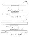
- FIG. 1illustrates an existing contact element engaging a metal pad on a substrate.
- a connector 100includes a contact element 102 for making an electrical connection to a metal pad 104 on a substrate 106 .
- the connector 100can be a wafer probe card and the contact element 102 is then a probe tip for engaging the pad 104 .
- a film 108which can be an oxide film or an organic film, forms on the surface of the pad 104 .
- the contact element 102When the contact element 102 engages the pad 104 , the contact element 102 must pierce through the film 108 in order to make a reliable electrical connection to the pad 104 .
- the piercing of the film 108can be performed by a wiping action or a piercing action of contact element 102 when the contact element 102 engages the pad 104 .
- FIG. 2 aillustrates the existing contact element 100 being applied to contact a solder ball 200 formed on a substrate 202 .
- the contact element 102contacts the solder ball 200 , such as for testing, the contact element 102 applies a piercing action which often results in the formation of a crater 204 on the top surface (also called the base surface) of the solder ball 200 .
- FIGS. 2 b and 2 cillustrate the result of attaching the solder ball 200 to a metal pad 210 of a substrate 212 .
- solder reflowFIG. 2 c
- the solder ball 200is attached to the metal pad 210 .
- a void 214is formed at the solder ball interface due to the presence of the crater 204 on the top surface of the solder ball 200 .
- the presence of the void 214can affect the electrical characteristics of the connection and more importantly, degrades the reliability of the connection.
- stamped metal spring elementsin particular, become brittle and difficult to manufacture as the dimensions are scaled down, rendering them unsuitable for accommodating electronic components with normal positional variations. This is particularly true when the spacing between the contacts scales below one millimeter, as well as where the electrical path length requirement also scales to below one millimeter to minimize inductance and meet high frequency performance requirements. At this size, spring elements made by existing manufacturing technologies become even more brittle and less elastic and cannot accommodate normal variations in system coplanarity and positional misalignments with a reasonable insertion force of about 30 to 40 grams per contact.
- an electrical contact elementthat can provide a controlled wiping action on a metal pad, particularly for pads with a pitch of less than 50 microns. It is also desirable that the wiping action provides a wiping distance of up to 50% of the contact pad. Furthermore, when electrical contact to solder balls are made, it is desirable to have an electrical contact element that can provide a controlled wiping action on the solder ball without damaging the contact surface of the solder ball.
- FIG. 1is a schematic diagram of an existing contact element engaging a metal pad on a substrate.
- FIG. 2 ais schematic diagram of an existing contact element contacting a solder ball.
- FIGS. 2 b and 2 care schematic diagrams illustrating the result of attaching a damaged solder ball to a metal pad of a substrate.
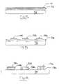
- FIGS. 3 a and 3 bare schematic diagrams of enlarged, perspective sectional views of a beam ball grid array (BBGA) system of the present invention and its attachment to a printed circuit board (PCB).
- BBGAbeam ball grid array
- PCBprinted circuit board
- FIGS. 3 c and 3 dare schematic diagrams of sectional views of two respective contact schemes used to electrically connect the contact system of FIG. 3 a to a PCB.
- FIG. 3 eis a schematic diagram of the structure for cradling a solder ball, in accordance with the configuration shown in FIGS. 3 a and 3 b.
- FIG. 3 fis a schematic diagram of a plan view of the contact arm array shown in FIG. 3 a.
- FIG. 3 gis a schematic diagram of a plan view of several different exemplary contact arm designs.
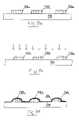
- FIG. 4 ais a schematic diagram of a cross-sectional view of an exemplary surface mount version of a beam land grid array (BLGA) system and its attachment to a PCB.
- BLGAbeam land grid array
- FIG. 4 bis a schematic diagram of a cross-sectional view of an exemplary separable version of a BLGA system and its attachment to a PCB.
- FIG. 5is a schematic diagram of an enlarged sectional view of exemplary contact arms for a BLGA contact array.
- FIG. 6is a schematic diagram of an enlarged perspective view of exemplary contact arm designs.
- FIG. 7is a schematic diagram of a perspective view of a connector according to one configuration of the present invention.
- FIG. 8is a schematic diagram of an exemplary connector including contact elements formed using multiple layers of metals according to another configuration of the present invention.
- FIGS. 9 a and 9 bare schematic diagrams of cross-sectional views of an exemplary connector according to one configuration of the present invention.
- FIGS. 10 a and 10 bare schematic diagrams of cross-sectional views of an exemplary connector according to an alternate configuration of the present invention.
- FIG. 11is a schematic diagram of a cross-sectional view of an exemplary connector according to an alternate configuration of the present invention.
- FIG. 12is a schematic diagram of a perspective view of an exemplary connector according to an alternate configuration of the present invention.
- FIGS. 13 a to 13 care schematic diagrams of cross-sectional views of one configuration of a connector being applied in a hot-swapping operation.
- FIGS. 14 a and 14 bare two schematic diagrams that show configurations of a circuitized connector in accordance with the present invention.
- FIG. 15 ais a schematic diagram of a cross-sectional view of an exemplary connector including a coaxial contact element according to an alternate configuration of the present invention.
- FIG. 15 bis a schematic diagrams of a top view of the coaxial contact element of FIG. 15 a.
- FIG. 16a schematic diagram that shows the mating of an LGA package to a PC board through the connector of FIG. 15 a.
- FIGS. 17 a to 17 hare schematic diagrams that show cross-sectional views of the exemplary processing steps for forming the connector of FIG. 9 a according to one implementation of the present invention.
- FIGS. 18 a and 18 bare schematic diagrams that show cross-sectional views of the exemplary processing steps for forming a connector according to an alternate implementation of the present invention.
- FIGS. 19 a – 19 dare flowcharts showing the steps of an exemplary method for making a connector in accordance with an alternate implementation of the present invention.
- FIG. 20is a schematic diagram of a cross-sectional view of an exemplary resist film applied to a sheet of spring material in accordance with the method shown in FIGS. 19 a – 19 d.
- FIG. 21is a schematic diagram of a cross-sectional view of UV light being applied to the resist film, in accordance with the method shown in FIGS. 19 a – 19 d.
- FIG. 22is a schematic diagram of a plan view of an exemplary sheet of contact elements formed in accordance with the method shown in FIGS. 19 a – 19 d.
- FIG. 23 ais a schematic diagram of a view of each layer of an exemplary stack up used in one of the steps of the method shown in FIGS. 19 a – 19 d.
- FIG. 23 bis a schematic diagram of a side view of the assembled stack up shown in FIG. 23 a.
- FIG. 24is a schematic diagram of an exploded perspective view of an exemplary stack-up in accordance with one configuration of the present invention.
- FIG. 25is a schematic diagram of an enlarged partial top plan view of an exemplary spacer layer used in the stack-up shown in FIG. 1 .
- FIGS. 26 and 27are schematic diagrams of cross-sectional views of an exemplary ball bearing configured die inserted into a spacer layer used in the stack-up shown in FIG. 1 .
- FIG. 28is a schematic diagram of a top plan view of an exemplary
- FIG. 29is a schematic diagram of a cross-sectional side view of an alternate configuration of a spring element sheet after pressing.
- FIG. 30 ais a schematic diagram that illustrates formation of three dimensional features in an unpatterned spring sheet, according to one configuration of the invention.
- FIG. 30 billustrates a cross-sectional view of a standard beam spring element of an elastic contact, according to one configuration of the invention.
- FIG. 30 cillustrates a cross-sectional view of a torsional beam spring element of an elastic contact, according to one configuration of the invention.
- FIG. 31 ais a flowchart of an exemplary method for batch forming spring elements in accordance with the present invention.
- FIG. 31 bis a flowchart of an exemplary method for batch forming spring elements as shown in FIG. 30 .
- FIGS. 3 a and 3 bare cross-sectional views of a beam ball grid array (BBGA) system constructed in accordance with the present invention.
- solder balls 302provide a method of establishing an electrical contact between the device, packages, or module 304 , and a carrier 306 .
- the solder balls 302are shown disposed within plated through holes or vias 308 that have been fabricated into the carrier 306 by printed circuit techniques.
- the solder balls 302are given elasticity by virtue of their suspension upon flexible contact arms 310 formed as part of a layer 312 .
- the contact arms 310cradle the solder ball 302 , as shown in FIG. 3 e , and provide a spring-like support as shown in FIGS. 3 c and 3 d.
- An array of contact arms 310is fabricated in layer 312 , as better observed with reference to FIG. 3 f .
- Different design patterns for the contact arms 310are respectively illustrated by elements 310 a , 310 b , 310 c , and 310 d in FIG. 3 g.
- the fabricationcontinues with the attachment of the structure 300 to a pad 314 of a PCB 316 by means of electrical contact elements 318 , which may include beam land grid array (BLGA) contact elements, a LGA, a pin grid array (PGA), or other types of contact elements as described below.
- electrical contact elements 318may include beam land grid array (BLGA) contact elements, a LGA, a pin grid array (PGA), or other types of contact elements as described below.
- the carrier 306makes electrical contact with the PCB 316 by means of a solder ball 320 that touches the pad 314 .
- the carrier 306makes contact with the pad 314 by means of contact arms 318 .
- the contact arms 310can be stamped or etched with the desired geometry. As will be described in greater detail hereinafter, they are then assembled in a PCB-like fabrication process.
- FIG. 4 ais a cross-sectional view of a surface mount version of a BLGA electrical contact element 400 constructed in accordance with the present invention.
- the BLGA systemincludes a carrier layer 402 having an array of arms 404 that form elastic elements out of the plane of the carrier 402 .
- the angle, thickness, and number of the arms 404can be readily changed to provide specific design features such as contact force, current carrying capacity, and contact resistance.
- the carrier 402is shown making electrical contact with a PCB 406 , by means of a solder ball 408 that touches a pad 410 .
- the arms 404can have shapes similar to arms 310 a–d in FIG. 3 a.
- FIG. 4 bis a cross-sectional view of a separable version of a BLGA contact element 400 a constructed in accordance with the present invention, including the carrier 402 making contact with the pad 410 by means of BLGA contact wipers 412 , which are similar to the contact arms 404 at the top of the carrier 402 .
- FIG. 5shows a cross-sectional view of a connector 500 in accordance with the present invention, including showing some exemplary dimensions for the size of the portions of the contact element 502 .
- the spacing between the distal ends of the facing spring portions 504is 5 mils.
- the height of the contact element 502 from the surface of the substrate to the top of the spring portionis 10 mils.
- the width of a via through the substratecan be on the order of 10 mils.
- the width of the contact element 502 from the outer edge of one base portion to the outer edge of the other base portionis 16 mils.
- Contacts of this sizecan be formed in accordance with the method of the invention as described below, allowing connectors with a pitch well below 50 mils and on the order of 20 mils or less. It is noted that these dimensions are merely exemplary of what can be achieved with the present invention and one skilled in the art will understand from the present disclosure that a contact element with larger or smaller dimensions could be formed.
- the following mechanical propertiescan be specifically engineered for a contact element or a set of contact elements, to achieve certain desired operational characteristics.
- the contact force for each contact elementcan be selected to ensure either a low resistance connection for some contact elements or a low overall contact force for the connector.
- the elastic working range of each contact elementcan be varied.
- the vertical height of each contact elementcan be varied.
- the pitch or horizontal dimensions of the contact elementcan be varied.
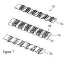
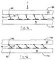
- a plurality of contact arm designsare shown for either a BBGA or a BLGA system.
- these contactscan be either stamped or etched into a spring-like structure, and can be heat treated before or after forming.
- FIG. 7is an exploded perspective view showing the assembly of a connector 700 according to one configuration of the present invention.
- the connector 700includes a first set of contact elements 702 that are located on a first major surface of a dielectric substrate 704 and a second set of contact elements 706 that are located on a second major surface of the substrate 704 .
- Each pair of contact elements 702 and 706is preferably aligned with a hole 708 formed in the substrate 704 .
- Metal tracesare formed through the hole 708 to connect a contact element from the first major surface to a contact element from the second major surface.
- FIG. 7shows the connector 700 during an intermediate step in the manufacturing process for forming the connector. Therefore, the array of contact elements is shown as being connected together on a sheet of metal or metallic material from which they are formed.
- the metal sheet between the contact elementsis patterned to remove unwanted portions of the metal sheet, so that the contact elements are isolated (i.e., singulated) as needed. For example, the metal sheet can be masked and etched to singulate some or all of the contact elements.
- the connector of the present inventionis formed as follows. First, the dielectric substrate 704 including conductive paths between the top surface and the bottom surface is provided. The conductive paths can be in the form of vias or an aperture 708 . In one configuration, the dielectric substrate 704 is a piece of any suitable dielectric material with conductive plated through holes. A conductive metal sheet or a multilayer metal sheet is then patterned to form an array of contact elements including a base portion and one or more elastic portions. The contact elements, including the spring portions, can be formed by etching, stamping, or other means. The metal sheet is attached to the first major surface of the dielectric substrate 704 .
- a second conductive metal sheet or multilayer metal sheetis similarly patterned and attached to the second major surface of the dielectric substrate 704 .
- the metal sheetscan then be patterned to remove unwanted metal from the sheets, so that the contact elements are isolated from each other (i.e., singulated) as needed.
- the metal sheetscan be patterned by etching, scribing, stamping, or other means.
- the protrusion of the elastic portionscan be formed after the metal sheet, including patterned contact elements, has been attached to the dielectric substrate.
- the unwanted portions of the metal sheetscan be removed before the contact elements are formed. Also, the unwanted portions of the metal sheets can be removed before the metal sheets are attached to the dielectric substrate.
- conductive tracesare formed in the plated through holes 708 and also on the surface of the dielectric substrate 704 in a ring-shaped pattern 710 encircling each plated through hole. While the conductive ring 710 can be provided to enhance the electrical connection between the contact elements on the metal sheet and the conductive traces formed in the dielectric layer 704 , the conductive ring 710 is not a required component of the connector 700 .
- the connector 700can be formed by using a dielectric substrate including through holes that are not plated. A metal sheet including an array of contact elements can be attached to the dielectric substrate. After the metal sheet is patterned to form individual contact elements, the entire structure can then be plated to form conductive traces in the through holes, connecting the contact elements through the holes to the respective terminals on the other side of the dielectric substrate.
- FIG. 8illustrates a connector 800 including contact elements formed using multiple layers of metals according to another configuration of the present invention.
- the connector 800includes a multilayer structure for forming a first group of contact elements 802 and a second group of contact elements 804 .
- the first group of contact elements 802is formed using a first metal layer 806 and the second group of contact elements 804 is formed using a second metal layer 808 .
- the first metal layer 806 and the second metal layer 808are isolated by a dielectric layer 810 .
- Each metal layeris patterned so that a group of contact elements is formed at desired locations on the specific metal layer.
- the contact elements 802are formed in the metal layer 806 at predefined locations, while the contact elements 804 are formed in the metal layer 808 at locations not occupied by the contact elements 802 .
- the different metal layersmay include metal layers with different thicknesses or different metallurgies, so that the operating properties of the contact elements can be specifically tailored.
- the contact elements of the connector 800can be made to exhibit different electrical and mechanical properties.
- the connector 800can be formed using the following process sequence.
- the first metal layer 806is processed to form the first group of contact elements 802 .
- the metal layer 806can then be attached to a dielectric substrate 812 .
- an insulating layersuch as the dielectric layer 810 , is located over the first metal layer 806 .
- the second metal layer 808can be processed to form the contact elements and attached to the dielectric layer 810 .
- Via holes and conductive tracesare formed in the dielectric substrate 812 and in the dielectric layer 810 as needed to provide a conductive path between each contact element to a respective terminal 814 on the opposing side of the substrate 812 .
- FIGS. 9 a and 9 bare cross-sectional views of a connector according to one configuration of the present invention.
- FIGS. 9 a and 9 billustrate a connector 900 connected to a semiconductor device 910 including metal pads 912 formed on a substrate 914 as contact points.
- the semiconductor device 910can be a silicon wafer where the metal pads 912 are the metal bonding pads formed on the wafer.
- the semiconductor device 910can also be a LGA package where the metal pads 912 represent the “lands” or metal connection pads formed on the LGA package.
- the coupling of the connector 900 to semiconductor device 910 in FIGS. 9 a and 9 bis illustrative only and is not intended to limit the application of the connector 900 to connecting with wafers or LGA packages only.
- FIGS. 9 a and 9 billustrate the connector 900 turned upside down to engage the semiconductor device 910 .
- the use of directional terms such as “above” and “top surface” in the present descriptionis intended to describe the relative positional relationship of the elements of the connector as if the connector is positioned with the contact elements facing upward.
- the connector 900includes an array of contact elements 902 located on a substrate 904 . Because the connector 900 can be built be for connecting to semiconductor devices at semiconductor scales, the connector 900 is usually formed using materials that are commonly used in semiconductor fabrication processes.
- the substrate 904is made of quartz, silicon, or a ceramic wafer and the contact elements 902 are located on a dielectric layer which could be a spin on silica (SOS), spin on glass (SOG), boron phosphorus tetraethoxysilane (BPTEOS), or tetraethoxysilane (TEOS) layer formed on the top surface of the substrate 904 .
- SOSspin on silica
- SOGspin on glass
- BPTEOSboron phosphorus tetraethoxysilane
- TEOStetraethoxysilane
- the array of contact elements 902is typically formed as a two-dimensional array arranged to mate with corresponding contact points on the semiconductor device 910 to be contacted.
- the connector 900is formed to contact metal pads having a pitch of 50 microns or less.
- Each contact element 902includes a base portion 906 attached to the top surface of the substrate 904 and a curved or linear spring portion 908 extending from the base portion 906 .
- the spring portion 908has a proximal end contiguous with the base portion 906 and a distal end projecting above the substrate 904 .
- the spring portion 908is formed to curve away or angle away from a plane of contact, which is the surface of the contact point to which the contact element 902 is to be contacted, the surface of the metal pad 912 .
- the spring portion 908is formed to have a concave curvature with respect to the surface of the substrate 904 , or is formed to be angled away from the surface of the substrate 904 .
- the spring portion 908curves or angles away from the surface of the metal pad 912 , which provides a controlled wiping action when engaging the metal pad 912 .
- an external biasing forcedenoted F in FIG. 9 a
- Fan external biasing force
- the spring portion 908 of the contact element 902engages the respective metal pad 912 in a controlled wiping action, so that each contact element 902 makes an effective electrical connection to the respective pad 912 .
- the curvature or angle of the contact elements 902ensures that the optimal contact force is achieved concurrently with the optimal wiping distance.
- the wiping distanceis the amount of travel the distal end of the spring portion 908 makes on the surface of the metal pad 912 when contacting the metal pad 912 .
- the contact forceis on the order of five to 100 grams depending on the application, and the wiping distance is on the order of five to 400 microns.
- the spring portion 908enables a large elastic working range. Specifically, because the spring portion 908 can move in both the vertical and the horizontal directions, an elastic working range on the order of the electrical path length of the contact element 902 can be achieved.
- the “electrical path length” of the contact element 902is defined as the distance the electrical current has to travel from the distal end of the spring portion 908 to the base portion 906 of the contact element 902 .
- the contact elements 902have an elastic working range that spans the entire length of the contact elements, which enables the connector to accommodate normal coplanarity variations and positional misalignments in the semiconductor or electronic devices to be connected.
- the contact elements 902are formed using a conductive metal that can also provide the desired elasticity.
- the contact elements 902are formed using titanium (Ti) as a support structure that can later be plated to obtain a desired electrical and/or elastic behavior.
- the contact elements 902are formed using a copper alloy (Cu-alloy) or a multilayer metal sheet such as stainless steel coated with a copper-nickel-gold (Cu/Ni/Au) multilayer metal sheet.
- the contact elements 902are formed using a small-grained copper beryllium (CuBe) alloy and then plated with electroless nickel-gold (Ni/Au) to provide a non-oxidizing surface.
- the contact elements 902are formed using different metals for the base portions and the spring portions.
- the contact element 902is shown as having a rectangular shaped base portion 906 with one spring portion 908 .
- the contact element of the present inventioncan be formed in a variety of configurations and each contact element only needs to have a base portion sufficient for attaching the spring portion to the substrate.
- the base portioncan assume any shape and can be formed as a circle or other useful shape for attaching the contact element to the substrate.
- a contact elementcan include multiple spring portions extending from the base portion.
- FIGS. 10 a and 10 billustrate a connector 1000 according to an alternate configuration of the present invention.
- the connector 1000includes an array of contact elements 1002 formed on a substrate 1004 .
- Each contact element 1002includes a base portion 1006 and two curved spring portions 1008 and 1010 extending from the base portion 1006 .
- the spring portions 1008 and 1010have distal ends, projecting above the substrate 1004 and facing towards each other.
- Other characteristics of the spring portions 1008 and 1010are the same as spring portion 908 . That is, the spring portions 1008 and 1010 curve away from a plane of contact and each has a curvature disposed to provide a controlled wiping action when engaging a contact point of a semiconductor device to be contacted.
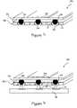
- the connector 1000can be used to contact a semiconductor device 1020 , such as a BGA package, including an array of solder balls 1022 mounted on a substrate 1024 as contact points.
- FIG. 10 billustrates the connector 1000 being fully engaged with the semiconductor device 1020 .
- the connector 1000can also be used to contact metal pads, such as pads on a land grid array package. However, using the connector 1000 to contact solder balls provides particular advantages.
- the contact elements 1002contact the respective solder balls 1022 along the side of the solder balls. No contact to the base surface of the solder ball 1022 is made. Thus, the contact elements 1002 do not damage the base surface of the solder balls 1022 during contact, and effectively eliminate the possibility of void formation when the solder balls 1022 are subsequently reflowed for permanent attachment.
- the contact elements 1002provide a controlled wiping action when contacting the respective solder balls 1022 . In this manner, an effective electrical connection can be made without damaging the surface of the solder balls 1022 .
- the connector 1000is scalable and can be used to contact solder balls having a pitch of 250 microns or less.
- each contact element 1002has a large elastic working range on the order of the electrical path length, the contact elements 1002 can accommodate a large range of compression. Therefore, the connector of the present invention can be used effectively to contact conventional devices having normal coplanarity variations or positional misalignments.
- FIGS. 11 and 12illustrate connectors according to alternate configurations of the present invention.
- a connector 1100includes a contact element 102 formed on a substrate 1104 .
- Contact element 1102includes a base portion 1106 , a first curved spring portion 1108 , and a second curved spring portion 1110 .
- the first spring portion 1108 and the second spring portion 1110have distal ends that point away from each other.
- the contact element 1102can be used to engage a contact point including a metal pad or a solder ball.
- contact element 1102When used to engage a solder ball, contact element 1102 cradles the solder ball between the first and second spring portions 1108 and 1110 , similar to what is shown in FIG. 3 e .
- the first and second spring portions 1108 and 1110contact the side surface of the solder ball in a controlled wiping motion in a direction that curves away from the plane of contact of the solder ball.
- FIG. 12illustrates a contact element 1200 located on a substrate 1202 .
- the contact element 1200includes a base portion 1204 , a first curved spring portion 1206 extending from the base portion 1204 , and a second curved spring portion 1208 extending from the base portion 1204 .
- the first spring portion 1206 and the second spring portion 1208project above the substrate 1202 in a spiral configuration.
- the contact element 1200can be used to contact a metal pad or a solder ball. In both cases, the first and second spring portions 1206 and 1208 curve away from the plane of contact and provide a controlled wiping action.
- FIGS. 13 a to 13 care cross-sectional views of a connector 1300 which can, for example, be applied in a hot-swapping operation.
- the connector 1300is shown in an unloaded condition.
- the connector 1300is to be connected to a land grid array (LGA) package 1320 and a printed circuit board (PC board) 1330 .
- a pad 1322 on the LGA package 1320represents a power connection (that is, either the positive power supply voltage or the ground voltage) of the integrated circuit in the LGA package 1320 which is to be connected to a pad 1335 on the PC board 1330 .
- the pad 1332is electrically active or “powered-up”.
- a pad 1324 on the LGA package 1320represents a signal pin of the integrated circuit which is to be connected to a pad 1334 on the PC board 1330 .
- the power pad 1322should be connected to pad 1332 prior to the signal pad 1324 being connected to pad 1334 .
- the connector 1300includes contact elements 1304 and 1306 in a substrate 1302 which have an extended height and a larger elastic working range than contact elements 1308 and 1310 , such that a hot-swapping operation between the LGA package 1320 and the PC board 1330 is realized using the connector 1300 .
- the height of the contact elements 1304 and 1306is selected to obtain the desired contact force and desired spacing to achieve a reliable hot-swapping operation.
- FIG. 13 billustrates an intermediate step during the mounting process of the LGA package 1320 to the PC board 1330 using the connector 1300 .
- pad 1322 and pad 1332will make electrical connections to respective contact elements 1304 and 1306 prior to the pads 1324 and 1334 making connection to contact elements 1308 and 1310 .
- the power connection between the LGA package 1320 and the PC board 1330is established before the signal pads are connected.
- FIG. 13 cillustrates the mounting of the LGA package 1320 to the PC board 1330 in a fully loaded condition.
- the LGA package 1320is compressed against the connector 1300 so that contact element 1308 engages the signal pad 1324 .
- the PC board 1330is compressed against the connector 1300 so that contact element 1310 engages the pad 1334 .
- the LGA package 1320is thus mounted onto the PC board 1330 .
- the taller contact elements 1304 , 1306are compressed more to allow the shorter contact elements 1308 , 1310 to engage, the contact force required for the connector will increase.
- the taller contact elements 1304 , 1306can be designed with a lower spring constant than the shorter contact elements 1308 , 1310 such that all contact elements are at the optimal contact force in the fully loaded condition.
- FIG. 14 aillustrates one configuration of a circuitized connector 1400 in accordance with the present invention.
- the connector 1400includes a contact element 1404 on the top surface of a dielectric substrate 1402 connected to a contact element 1406 on the bottom surface of dielectric substrate 1402 .
- the contact element 1404is connected to a surface mounted electrical component 1410 and an embedded electrical component 1412 .
- the electrical components 1410 and 1412may be decoupling capacitors, for example, which are positioned on the connector 1400 so that the capacitors can be placed as close to the electronic component as possible. In conventional integrated circuit assembly, such decoupling capacitors are usually placed on the printed circuit board distant from the electronic component.
- the decoupling capacitorscan be placed as close to the electronic component as possible to enhance the effectiveness of the decoupling capacitors.
- Other electrical components that may be used to circuitize the connectorinclude a resistor, an inductor, and other passive or active electrical components.
- FIG. 14 billustrates another configuration of a circuitized connector according to the present invention.
- Connector 1420includes a contact element 1424 on a dielectric substrate 1422 coupled to a solder ball terminal 1426 through a via 1428 .
- the contact element 1424is connected to a surface mounted electrical component 1430 and to an embedded electrical component 1432 .
- the connector 1420further illustrates that the placement of the terminal 1426 does not have to be aligned with the contact element 1424 as long as the contact element is electrically coupled to the terminal, such as through the via 1428 .
- a connector in accordance with the present inventioncan be constructed without a relief hole in the substrate.
- the electrical contact or viacan be defined in an offset hole or in any suitable manner to provide electrical connections internally or to opposite sides of the substrate.
- a connectorcan include one or more coaxial contact elements.
- FIGS. 15 a and 15 bshow a connector 1500 including a coaxial contact element according to one configuration of the present invention.
- the connector 1500includes a first contact element 1504 and a second contact element 1506 formed on the top surface of a dielectric substrate 1502 .
- the contact elements 1504 and 1506are formed in proximity to, but electrically isolated from, each other.
- the contact element 1504includes a base portion formed as an outer ring of an aperture 1508 while the contact element 1506 includes a base portion formed as an inner ring of the aperture 1508 .
- Each of the contact elements 1504 , 1506includes three elastic portions ( FIG. 15 b ).
- the elastic portions of the contact element 1504do not overlap with the elastic portions of the contact element 1506 .
- the contact element 1504is connected to a contact element 1510 on the bottom surface of the dielectric substrate 1502 through at least one via 1512 .
- the contact elements 1504 and 1510form a first current path, referred to as the outer current path of the connector 1500 .
- the contact element 1506is connected to a contact element 1514 on the bottom surface of the dielectric substrate 1502 through a metal trace 1516 formed in the aperture 1508 .
- the contact elements 1506 and 1514form a second current path, referred to as the inner current path of the connector 1500 .
- the connector 1500can be used to interconnect a coaxial connection on a LGA package 1520 to a coaxial connection on a PC board 1530 .
- FIG. 16illustrates the mating of the LGA package 1520 to the PC board 1530 through the connector 1500 .
- the contact element 1504engages a pad 1522 on the LGA package 1520 .
- the contact element 1510engages a pad 1532 on the PC board 1530 .
- the outer current path between pad 1522 and pad 1532is formed.
- the outer current pathconstitutes a ground potential connection.
- the contact element 1506engages a pad 1524 on the LGA package 1520 while the contact element 1514 engages a pad 1534 on the PC board 1530 .
- the inner current path between pad 1524 and pad 1534is formed.
- the inner current pathconstitutes a high frequency signal.
- a particular advantage of the connector 1500is that the coaxial contact elements can be scaled to dimensions of one millimeter or less. Thus, the connector 1500 can be used to provide a coaxial connection even for small geometry electronic components.
- FIGS. 17 a to 17 hillustrate the processing steps for forming the connector 900 of FIG. 9 a , according to one configuration of the present invention.
- a substrate 1700 on which the contact elements are to be locatedis provided.
- the substrate 1700can be a silicon wafer or ceramic wafer with previously defined circuits, for example, and may include a dielectric layer formed thereon (not shown in FIG. 17 a ).
- the dielectric layer, of SOS, SOG, BPTEOS, or TEOS for example,can be formed on the substrate 1700 for isolating the contact elements from the substrate 1700 .
- a support layer 1702is formed on the substrate 1700 .
- the support layer 1702can be a deposited dielectric layer, such as an oxide or nitride layer, a spin-on dielectric, a polymer, or any other suitable etchable material.
- the support layer 1702can be deposited by a number of different processes, including chemical vapor deposition (CVD), plasma vapor deposition (PVD), a spin-on process, or when the substrate 1700 is not covered by a dielectric layer or a conductive adhesive layer, the support layer 1702 can be grown using an oxidation process commonly used in semiconductor manufacturing.
- a mask layer 1704is formed on the top surface of the support layer 1702 .
- the mask layer 1704is used in conjunction with a conventional lithography process to define a pattern on the support layer 1702 using the mask layer 1704 .
- a mask patternincluding regions 1704 a to 1704 c , is formed on the surface of the support layer 1702 defining areas of the support layer 1702 to be protected from subsequent etching.
- an anisotropic etching processis performed using regions 1704 a to 1704 c as a mask.
- the anisotropic etching processthe portions of the support layer 1702 not covered by a patterned mask layer is removed. Accordingly, support regions 1702 a to 1702 c are formed.
- the mask pattern including regions 1704 a to 1704 cis subsequently removed to expose the support regions ( FIG. 17 d ).
- the support regions 1702 a to 1702 care then subjected to an isotropic etching process.
- An isotropic etching processremoves material under etch in the vertical and horizontal directions at substantially the same etch rate.
- the isotropic etchingis a plasma etching process using SF 6 , CHF 3 , CF 4 , or other well known chemistries commonly used for etching dielectric materials.
- the isotropic etching processis a wet etch process, such as a wet etch process using a buffered oxide etch (BOE).
- BOEbuffered oxide etch
- a metal layer 1706is formed on the surface of the substrate 1700 and the surface of support regions 1702 a to 1702 c .
- the metal layer 1706can be a copper layer, a copper alloy (Cu-alloy) layer, or a multilayer metal deposition such as titanium-coated with copper-nickel-gold (Cu/Ni/Au).
- the contact elementsare formed using a small-grained copper beryllium (CuBe) alloy, and are then plated with electroless nickel-gold (Ni/Au) to provide a non-oxidizing surface.
- the metal layer 1706can be deposited by a CVD process, electro plating, sputtering, PVD, or other conventional metal film deposition techniques.
- a mask layeris deposited and patterned into mask regions 1708 a to 1708 c using a conventional lithography process.
- the mask regions 1708 a to 1708 cdefine areas of the metal layer 1706 to be protected from subsequent etching.
- each of the metal portions 1706 a to 1706 cincludes a base portion formed on the substrate 1700 and a curved spring portion formed on a respective support region ( 1702 a to 1702 c ). Accordingly, the curved spring portion of each metal portion assumes the shape of the underlying support region, projecting above the surface of the substrate 1700 .
- the support regions 1702 a to 1702 care removed ( FIG. 17 h ), such as by using a wet etch, an anisotropic plasma etch, or other etch process. If the support layer is formed using an oxide layer, a buffered oxide etchant can be used to remove the support regions. As a result, free standing contact elements 1710 a to 1710 c are formed on the substrate 1700 .
- a connectorcan be fabricated with contact elements having a variety of properties. For example, a first group of contact elements can be formed with a first pitch, while a second group of contact elements can be formed with a second pitch that is greater or smaller than the first pitch. Other variations in the electrical and mechanical properties of the contact element are possible.
- FIGS. 18 a and 18 billustrate the first and last processing steps for forming a circuitized connector similar to the connector 1400 of FIG. 14 a , according to an alternate configuration of the present invention.
- a substrate 1800 including predefined circuitry 1802is provided.
- the predefined circuitry 1802can include interconnected metal layers or other electrical devices, such as capacitors, resistors, transistors, or inductors, which are typically formed in the substrate 1800 .
- a top metal portion 1804is formed on the top surface of the substrate 1800 to be connected to the contact element to be formed.
- a support layer 1806 and a mask layer 1808are formed on the top surface of the substrate 1800 .
- a process similar to that described above in connection with FIGS. 17 b to 17 gis used to form a contact element 1810 ( FIG. 18 b ).
- the contact element 1810is electrically connected to the circuit 1802 .
- additional functionalitycan be provided by the connector of the present invention.
- the circuit 1802can be formed to electrically connect certain contact elements together.
- the circuit 1802can also be used to connect certain contact elements to electrical devices such as a capacitor or an inductor formed in or on the substrate 1800 .
- fabricating the contact element 1810 as part of an integrated circuit manufacturing processprovides further advantages. Specifically, a continuous electrical path is formed between the contact element 1810 and the underlying circuit 1802 . There is no metal discontinuity or impedance mismatch between the contact element and the associated circuit. In some prior art connectors, a gold bond wire is used to form the contact element. However, such a structure results in gross material and cross-sectional discontinuities and impedance mismatch at the interface between the contact element and the underlying metal connections, resulting in undesirable electrical characteristics and poor high frequency operations.
- a connectoris provided with contact elements having different operating properties. That is, the connector can include heterogeneous contact elements where the operating properties of the contact elements can be selected to meet requirements in the desired application.
- the operating properties of a contact elementrefer to the electrical, mechanical, and reliability properties of the contact element.
- the electrical propertiescan be specifically engineered for a contact element or a set of contact elements to achieve certain desired operational characteristics.
- the DC resistance, the impedance, the inductance, and the current carrying capacity of each contact elementcan be varied.
- a group of contact elementscan be engineered to have lower resistance or to have low inductance.
- the contact elementscan also be engineered to display no or minimal performance degradation after environmental stresses such as thermal cycling, thermal shock and vibration, corrosion testing, and humidity testing.
- the contact elementscan also be engineered to meet other reliability requirements defined by industry standards, such as those defined by the Electronics Industry Alliance (EIA).
- EIAElectronics Industry Alliance
- the thickness of the spring portion of the contact elementcan be selected to give a desired contact force. For example, a thickness of about 30 microns typically gives a low contact force on the order of 10 grams or less, while a flange thickness of 40 microns gives a higher contact force of 20 grams for the same displacement.
- the width, length, and shape of the spring portioncan also be selected to give the desired contact force.
- the number of spring portions included in a contact elementcan be selected to achieve the desired contact force, the desired current carrying capacity, and the desired contact resistance. For example, doubling the number of spring portions roughly doubles the contact force and current carrying capacity, while roughly decreasing the contact resistance by a factor of two.
- specific metal composition and treatmentcan be selected to obtain the desired elasticity and conductivity characteristics.
- copper alloyssuch as beryllium copper
- metal multilayerscan be used to provide both excellent mechanical and electrical properties.
- a contact elementis formed using titanium (Ti) coated with copper (Cu), then with nickel (Ni), and finally with gold (Au) to form a Ti/Cu/Ni/Au multilayer.
- Tiprovides elasticity and high mechanical durability
- the Cuprovides conductivity
- Ni and Au layersprovide corrosion resistance.
- different metal deposition techniquessuch as plating or sputtering
- different metal treatment techniquessuch as alloying, annealing, and other metallurgical techniques can be used to engineer specific desired properties for the contact elements.
- the shape of the spring portioncan be designed to give certain electrical and mechanical properties.
- the height of the spring portion, or the amount of projection from the base portion,can also be varied to give the desired electrical and mechanical properties.
- FIGS. 19 a – 19 dare flowcharts of a method 1900 for forming contact elements in accordance with an alternate configuration of the present invention.
- FIGS. 20–23 bwill be discussed in the context of the discussion of the method 1900 .
- the method 1900also relates to batch fabrication of the contact elements using masking, etching, forming, and lamination techniques.
- the method 1900produces a plurality of highly engineered electrical contacts, capable of use in a separable connector such as in an interposer, or the contacts can be directly integrated into a substrate as a continuous trace that then functions as a permanent onboard connector.
- additional masking and etching steps to form the three dimensional spring portionsthey are created in flat arrays and are then formed into three dimensional shapes.
- a base spring material for the sheet of contactsis selected, such as beryllium copper (Be—Cu), spring steel, phosphorous bronze, or any other material with suitable mechanical properties (step 1902 ).
- Be—Cuberyllium copper
- spring steelspring steel
- phosphorous bronzeor any other material with suitable mechanical properties
- the proper selection of materialenables the contact elements to be engineered to have the desired mechanical and electrical properties.
- One factor in the selection of the base materialis the working range of the material.
- Working rangeis the range of displacement over which the contact element meets both contact force (load) and contact resistance specifications. For example, assume that the desired contact resistance is less than 20 milliohms and the maximum allowed contact load is 40 grams.
- the contact elementreaches a resistance range of less than 20 milliohms at 10 grams of load and then is carried over to the maximum load of 40 grams for the beam member, while maintaining a resistance of less than 20 milliohms, then the distance over which the contact element has traveled between 10 grams and 40 grams of load would be the working range of the contact.
- the sheetcan be heat treated prior to subsequent processing (step 1904 ). Whether the sheet is heated at this point in the process is determined by the type of material selected for the sheet. The heating is performed to move the material from a half-hard state into a hard state or highly-tensile state that provides desired mechanical properties for forming the contacts.
- a contact elementis designed and is copied into an array form, for use in batch processing (step 1906 ).
- the number of contacts in an arrayis a design choice, and can vary depending on the requirements for the connector.
- the arraysare repeated into a panel format, analogous to chips or die in a semiconductor wafer, resulting in a scalable design that lends itself to batch processing.
- the contact designis ported to a Gerber format, which is a translator that enables the design to be ported to a fabrication facility to produce the master slides or film to be used in the subsequent steps.
- the panel formatcan have anywhere between one and a large number of contacts, because the use of lithography permits placing a high density of contacts onto a panel.
- This high density of contactsprovides an advantage over existing methods in that a batch process can be used to singulate the contacts, as opposed to stamping and forming individual contacts.
- the method 1900permits a large number of contacts to be patterned, developed, and etched at once.
- a lithographically sensitive resist filmis then applied to both sides of the sheet (step 1908 and FIG. 20 ).
- a dry filmcan be used for larger feature sizes ranging from one to 20 mils, and a liquid resist can be used for feature sizes less than one mil.
- both the top and bottom of the sheetare exposed to ultraviolet (UV) light and then developed to define contact features in the resist (step 1910 and FIG. 21 ). Portions that are intended to be etched are left unprotected by the mask.
- UVultraviolet
- Using a lithographic process to define the contact elementsenables the printing of lines with a fine resolution, similar to that found in semiconductor manufacturing.
- the sheetis then etched in a solution specifically selected for the material being used (step 1912 ).
- Each particular material that can be selected for the sheettypically has a specific etch chemistry associated with it to provide the best etch characteristics, such as etch rate (i.e., how well and how fast the solution performs the etch). This is an important consideration in the context of throughputs.
- the etchant selectedalso effects other characteristics like the sidewall profile, or the straightness of a feature as seen in cross section.
- chemicals common in the industryare used, such as cupric chloride, ferric chloride, and sulfuric hydroxide.
- a batch forming toolis designed, based upon the artwork defined in step 1906 (step 1916 ).
- the batch forming toolincludes a plurality of ball bearings arranged, into an array format, preferably by being set into an array of openings in a support surface.
- the ball bearingscan be of different sizes, to apply different forces to the contacts, thereby imparting different mechanical characteristics to contacts on the same panel.
- the curvature of the ball bearingsis used to push the flanges away from the plane of the sheet.
- the flanges of the contactsare then formed in all three axes by applying the forming tool to the sheet, to produce the desired contact elements in a batch process (step 1918 ), as discussed in more detail with reference to FIGS. 24–30 below.
- the sheetcan be heat treated to relieve stress caused by the forming process (step 1920 ).
- the heating step 1920is optional, and is dependent upon the material selected for the sheet. Based upon the material and the size of the contacts to be defined on the sheet, heating may be performed to obtain the physical properties desired for optimal forming conditions.
- the sheetis then surface treated to enhance adhesion properties for a subsequent lamination process (step 1922 ). If there is inadequate adhesion, there is a propensity for the sheet to separate from a substrate or delaminate.
- Several methods for performing the surface treatingcan be used, including micro etching and a black oxide process.
- the micro etchingis used to pit the surface of the sheet, effectively creating a greater surface area (by making the surface rough and cratered) to promote better adhesion. However, if the micro etching is not properly controlled, it can lead to damage on the sheet.
- the black oxide processis a replacement process involving a self-limiting reaction in which an oxide is grown on the surface of the sheet. In this reaction, the oxygen diffuses only through a set thickness, thereby limiting the amount of oxide grown.
- the oxidehas a rough surface in the form of bumps, which helps to promote adhesion. Either the micro etching or the black oxide processes can be used for the surface treatment step, and a preference for one process over the other is a design choice.
- a low flow adhesion material and dielectric coreare processed with relief depressions or holes located beneath flange elements (step 1924 ). This is intended to prevent excess flow of material up on the flange during the lamination process. Should this flow happen, the contact properties would be altered, causing the contact element to be unsuitable for electrical and mechanical use.
- FIG. 23 ashows each layer of the stack up.
- Layer 1is a top press plate material
- Layer 2is a spacer material with a relief hole over the spring contact element
- Layer 3is a release material with a relief hole over the spring contact
- Layer 4is a top sheet of formed contact sheets
- Layer 5is an adhesion material with a relief hole beneath the spring contact
- Layer 6is a core dielectric with relief holes under and above the spring contact
- Layer 7is an adhesion material with a relief hole above the spring contact
- Layer 8is a bottom sheet of formed contact elements
- Layer 9is a release material with a relief hole below the spring contact
- Layer 10is a spacer material with a relief hole below the spring contact element
- Layer 11is a bottom press plate material
- the stack upis pressed under temperature conditions optimized for desired adhesions and flow conditions for the adhesion material (step 1928 and FIG. 23 b ). During this operation, the top and bottom contact sheets are bonded to a core dielectric material. After a cool down period, the stack up is removed from the press plates, leaving a panel comprised of Layers 4 – 8 (step 1930 ).
- the panel surfaces and openingsare then plated to electrically connect the top and bottom flanges (step 1932 ).
- This steptakes the top flange and electrically connects it to the bottom flange by a plating process known as an electroless process.
- the processeffectively deposits a conductive material on the top surface, into the through hole to connect both sheets of contact elements, and then onto the sheet on the other side of the substrate.
- the plating processcreates a route for an electrical current to travel from one side of the board to the other.
- a photosensitive resist filmis applied to both sides of the panel (step 1934 ).
- a patternis exposed and developed to define the individual contact elements (step 1936 ).
- a determinationis then made as to the contact finish type, either hard gold or soft gold (step 1938 ).
- Hard goldis used in specific applications where the numbers of insertions required are high, such as a test socket. Hard gold itself has impurities that cause the gold to be more durable. Soft gold is a pure gold, so it effectively has no impurities, and is typically used in the PCB or networking space, where the number of insertions is fairly low. For example, a package to board socket used in a PC (soft gold) will typically see on the order of one to 20 insertions, whereas other technology using hard gold will see a number of insertions between 10 and 1,000,000.
- the contact finish typeis a hard gold
- a partial etchingis performed to almost singulate the contact elements (step 1940 ).
- the resist filmis removed via a stripping process (step 1942 ).
- a new layer of resistis applied, covering both sides of the panel (step 1944 ).
- the previously etched areasare exposed and developed (step 1946 ).
- the panelis then submitted for electrolytic Cu/Ni/Au plating via a hard gold process (step 1948 ).
- the resistis removed to expose previous partially etched scribe lines (step 1950 ).
- the entire panelis etched using electrolytic Ni/Au as a hard mask to complete singulation of the contact array (step 1952 ).
- Final interposer outlinesare routed out of the panel to separate the panel into individual connector arrays (step 1954 ), and the method terminates (step 1956 ).
- step 1938If a soft gold finish is used (step 1938 ), then etching is used to completely singulate the contact elements (step 1960 ).
- the resist filmis removed via a stripping process (step 1962 ).
- Electroless Ni/Aualso known as a soft gold, is plated onto the panel to complete the contact elements (step 1964 ).
- Final interposer outlinesare routed out of the panel to separate the panel into individual connector arrays (step 1954 ), and the method terminates (step 1956 ).
- the soft gold finishing processsingulates the contacts prior to plating. Ni/Au will plate only on metal surfaces, and provides a sealing mechanism for the contact element his helps to prevent potential corrosive activity that could occur over the system life of the contact, since gold is virtually inert. Singulation prior to plating is a means to isolate or encapsulate the copper contact with another metal, resulting in cleaner imaging and a cleaner contact, which has a low propensity for shorting.
- FIG. 24shows an exemplary stack-up 2400 that can be used in step 1918 for batch forming spring elements in three dimensions in accordance with one configuration of the present invention.
- Stack-up 2400has a bottom press plate 2402 as its bottom layer.
- Bottom press plate 2402preferably includes at least two dowel pins 2404 or other aligning means such as reference holes, edges, or the like, for aligning the elements of stack-up 2400 .
- the material used for bottom press plate 2402can be any material with sufficient rigidity to support the force used for compressing the stack-up without deforming the press plate 2402 , for example, steel or aluminum. While stack-up 2400 is shown utilizing two dowel pins 2404 , any number of dowel pins can be used.
- a bottom spacer layer 2406(shown in partial top plan view in FIG. 25 ) is positioned above bottom press plate 2402 .
- bottom spacer layer 106is made of a softer material than bottom press plate 2402 , for example, metal or plastic. It is noted that layer 2406 could alternatively be made of a material similar to bottom press plate 2402 .
- Layer 2406has positioning holes 2408 , or other suitable means as discussed above, to align layer 2406 with bottom press plate 2402 .
- Layer 2406also has a plurality of holes 2410 . Each of holes 2410 is sized and shaped to hold a configurable die, for example, ball bearings 2412 , depicted in the enlarged view of FIG. 26 .
- configurable dierefers to elements that can be used to form or impart a shape in another structure, such as a deformable sheet.
- configurable diecould also be conical, pyramidal or other shapes.
- holes 2410 and configurable die 2412are formed in precise positions using photolithographic mask and etch technology in order to form an array that exactly matches a particular contact arrangement, for example a contact arrangement of a device to be contacted by the finished spring element sheet. This arrangement can be done inexpensively at micron accuracy, with very fast turnaround to accommodate various contact patterns.
- Ball bearings 2412 or other configurable dieare placed into holes 2410 by manual or mechanical means according to a desired pattern to form the spring elements or dome features that may then later be patterned and etched to form spring elements.
- Ball bearings 2412can have a slight interference fit so that they are pressed and held in position. As shown in FIGS. 26 and 27 , the height that the bearings protrude can be controlled by the hole diameter. Ball bearings 2412 can be inserted up to their equator or beyond for stability, as shown in FIG. 29 .
- Holes 2410are generally drilled slightly smaller than ball bearing 2412 , e.g., 0.025 mm or smaller.
- spacer layer 2406can retain the configurable die, such that the resulting spacer layer containing configurable die can operate as a die plate for shaping deformable sheets to form spring elements in the sheets.
- the resulting die platecontains three dimensional features corresponding in size and shape to the portions of individual configurable die protruding above the plane of spacer layer 2406 , imparting a three dimensional surface, for example, surface 2450 as depicted in FIG. 27 .
- the shape and size of features of surface 2450can be tailored by changing the shape and size of configurable die inserted in spacer layer 2406 .
- a predetermined designmay call for spring elements to have a shape of a circular arc as viewed in cross section, as illustrated for layer 2414 in FIG. 29 .
- a spherical or cylindrical diecould be used to impart such a design.
- the height that a configurable die protrudes above the planar surface portion of a die platecan be varied accordingly.
- Ball bearings 2412 or other configurable diecan be made of hardened tool steel or stainless steel and can vary in diameter depending upon the desired characteristics of the spring elements to be formed. Ball bearings 2412 could also be made of any other suitable material, such as AL 6061, AL 76075, chromium steel, or tungsten carbide. As an example, ball bearings 2412 can range in diameter from approximately 0.3 mm to approximately 127.0 mm. The depth of insertion of ball bearings 2412 into layer 2406 is limited by bottom press plate 2402 . The depth of insertion of ball bearings 2412 (as shown in FIGS. 26 and 27 ) can also be varied to provide different spring characteristics to individual spring elements. Additionally, ball bearings 2412 or other configurable die of different sizes or shapes can be utilized to achieve different spring characteristics.
- Sheet 2414contains spring elements defined in two dimensions and can be formed by various methods, including etching or stamping. An example of a spring element sheet with the elements defined in two dimensions is shown in FIG. 28 .
- the forming tool of step 1918thus comprises layers 2402 , 2406 , 2412 , 2418 and 2424 , which are applied to sheet 2414 to form three dimensional spring elements that are arranged, for example, in an array within sheet 2414 .
- the configurable die 2412can be arranged in a two dimensional pattern in spacer layer 2406 , such that the die positions in the resulting die plate correspond to the positions of at least some of the two dimensional spring elements arranged in spring sheet 2414 , when the die plate (not shown) is brought into contact with spring sheet 2414 .
- the pattern of configurable die 2412 placed within spacer layer 2406is arranged accordingly. In this manner, the configurable die 2412 deform only the two dimensional spring elements that are desired to be formed into three dimensional spring elements. Configurations may readily change by adding or removing regions of die that result in a new form or size of contact.”
- a spring element sheet 2414 ′without predefined spring elements may be used.
- Spring element sheet 2414 ′is a plain spring element sheet having only positioning holes 2416 to align sheet 2424 ′ to other layers.
- the present inventionoperates in the same manner, regardless of whether sheet 2414 or sheet 2414 ′ is used, except as noted below. For discussion proposes only, further discussion shall only refer to sheet 2414 , but is equally applicable to sheet 2414 ′.
- top spacer layer 2418is placed on top of sheet 2414 .
- Top spacer layer 2418has positioning holes 2420 for aligning layer 2418 with dowel pins 2404 , or other alignment means as discussed above.
- Top spacer layer 2418can also contain a plurality of openings 2422 that are complementary to configurable die 2412 , through which the spring elements are formed.
- the term “complementary”signifies that openings 2422 are substantially aligned with positions of configurable die 2412 when top spacer layer 2418 is brought into contact with spring sheet 2414 .
- local deformations of spring sheet 2414 around configurable die 2412can be accommodated substantially within openings 2422 when top spacer layer 2418 contacts spring sheet 2414 and deforms it over configurable die 2412 .
- Top spacer layer 2418may be constructed of similar or different materials as bottom spacer layer 2406 . Openings 2422 in layer 2418 could be smaller, the same size or larger than holes 2410 in bottom spacer layer 2406 . In this manner, some control over the final shape of the spring elements can be achieved by changing the size of openings 2422 . In addition, the thickness of top spacer layer 2418 can also help to determine the final height of the spring elements above the surface of the sheet 2414 .
- spacer layer 2418is made of a compliant material (for example, silicon rubber) substantially conformable around configurable die 2412 in order to form the spring elements on the contact area of configurable die 2412 , as shown in FIG. 29 .
- layer 2418can initially comprise a layer having uniform thickness that can conform to three dimensional shapes by deformation of surface 2419 , as shown in FIG. 29 .
- top spacer layer 2418can be designed as a top spacer sheet having a plurality of openings into which configurable die are pressed at defined locations. In this manner, top spacer layer 2418 forms a second die plate (not shown) that can be used to form spring elements below the plane of sheet 2414 . In this manner, when layer 2418 and layer 2406 are brought into contact with spring sheet 2414 , spring elements can be formed both above and below the plane of spring sheet 2414 .
- the pattern of configurable die in top spacer layer 2418are arranged so that the positions of individual die do not correspond to the same planar positions of configurable die in bottom spacer sheet 2406 .
- any planar position of spring sheet 2414can be contacted by a configurable die in either top spacer layer 2418 or bottom spacer sheet 2406 , both not both.
- every configurable die of each set of configurable dieeither arranged in the top spacer or bottom spacer, corresponds to a unique spring element position in spring sheet 2414 . Accordingly, when stack up 2400 is brought together, every two dimensional spring element to be formed into a three dimensional spring element is forced to protrude either above or below the plane of spring sheet 2414 .
- top press plate 2424is placed on top of top spacer layer 2418 .
- Top press plate 2424has positioning holes 2426 for alignment with dowel pins 2404 or other alignment means.
- Top press plate 2424is constructed of similar materials as bottom press plate 2402 . After the elements of stack-up 2400 have been assembled and aligned, preferably using dowel pins 2404 , pressure is applied to both top press plate 2424 and bottom press plate 2402 . This pressure forces configurable die 2412 against the underside of sheet 2414 , pushing the spring elements upward to form them in three dimensions, as shown in FIG. 29 .
- the amount of force required to form the spring elementsdepends upon the properties of the material being formed, and can be limited by the yield strength of the bottom press plate 2402 if desired. However, in view of the size and scale of the contact arms being formed, this is generally not an issue.
- domes 3010can be patterned and etched to form three dimensional contact elements.
- An electrical connector having a spring element formed by using a ball bearing in accordance with the present inventionhas unique characteristics. Pressing the spring element over the ball bearing causes the spring element to have a torsional force added to the spring force of the material, to provide additional spring characteristics. This results in unique physical configurations that provide the electrical connector with a better wiping action to an abutting electrical contact.
- the torsional forceexists any time there is a twisting of the material; in the present case, the material is formed around a spherical ball bearing, causing it to be twisted around the surface of the sphere, thus supplying a torsional force. It is noted that arrangements of configurable die with surfaces having shapes other than the aforementioned spherical ball bearings are contemplated in the present invention. Accordingly, the degree and nature of forces imparted into electrical contacts formed over a configurable die of the present invention can be varied.
- FIG. 30 billustrates in cross-section a conventional cantilever beam spring element 3020 that can form a spring element of a contact
- FIG. 30 cillustrates in cross-section a torsion beam spring element 3030 of a contact, according to configurations of the invention.
- a method 3100 for forming spring elements in three dimensionscan also be derived, as shown in FIG. 31 a .
- a base layer of ball bearings or other configurable dieis provided, with the ball bearings, for example, being arranged in a predetermined pattern corresponding to the location of the spring elements to be formed (step 3102 ).
- a spring element sheetis placed on top of the ball bearings, the spring elements being defined in two dimensions and positioned over ball bearings on the base layer (step 3104 ).
- the spring element sheetis then pressed against the ball bearings, with the ball bearings contacting the underside of the sheet, thereby pressing the spring elements above the plane of the sheet and forming the spring elements in three dimensions (step 3106 ).
- FIG. 31 billustrates an alternate method 3110 for forming spring elements from three dimensional structures (such as domes 3010 shown in FIG. 30 ).
- a configurable diefor example, a base layer of ball bearings is provided, with the ball bearings being arranged in a predetermined pattern corresponding to the location of the three dimensional domes to be formed (step 3114 ).
- a plain spring sheetis placed on top of the configurable die (step 3116 ).
- plainrefers to the fact that a plain spring sheet does not contain pre-patterned two dimensional spring elements before being pressed onto configurable die.
- the spring sheetis pressed against the configurable die, with the configurable die contacting the underside of the sheet, thereby pressing portions of the spring sheet above the plane of the sheet and forming surface three dimensional structures (also termed “three dimensional spring precursors”), for example, domes 3010 formed over ball bearings (step 3118 ).
- the spring sheet containing the three dimensional spring precursors, such as domesis then patterned and etched into three dimensional spring contact elements.
- individual domescan be patterned and etched through the entire spring sheet thickness to remove portions of the domes and form contacts having a structure, for example, similar to that of contact 1200 of FIG. 12 .
- a connector according to the present inventioncould be used as an interposer, a PCB connector, or could be formed as an integral part of a PCB.
- the scalability of the present inventionis not limited, and can be easily customized for production due to the lithographic techniques used and the simple tooling die used for forming the connector elements in three dimensions.
- the specificationmay have presented the method and/or process of the present invention as a particular sequence of steps. However, to the extent that the method or process does not rely on the particular order of steps set forth herein, the method or process should not be limited to the particular sequence of steps described. As one of ordinary skill in the art would appreciate, other sequences of steps may be possible. Therefore, the particular order of the steps set forth in the specification should not be construed as limitations on the claims. In addition, the claims directed to the method and/or process of the present invention should not be limited to the performance of their steps in the order written, and one skilled in the art can readily appreciate that the sequences may be varied and still remain within the spirit and scope of the present invention.
Landscapes
- Engineering & Computer Science (AREA)
- Microelectronics & Electronic Packaging (AREA)
- Computer Hardware Design (AREA)
- Power Engineering (AREA)
- Manufacturing & Machinery (AREA)
- Connecting Device With Holders (AREA)
Abstract
Description
Claims (10)
Priority Applications (3)
| Application Number | Priority Date | Filing Date | Title |
|---|---|---|---|
| TW094108354ATWI265657B (en) | 2004-03-19 | 2005-03-18 | Method and system for batch forming spring elements in three dimensions |
| US11/083,031US7597561B2 (en) | 2003-04-11 | 2005-03-18 | Method and system for batch forming spring elements in three dimensions |
| US11/787,976US7758351B2 (en) | 2003-04-11 | 2007-04-18 | Method and system for batch manufacturing of spring elements |
Applications Claiming Priority (3)
| Application Number | Priority Date | Filing Date | Title |
|---|---|---|---|
| US10/412,729US7056131B1 (en) | 2003-04-11 | 2003-04-11 | Contact grid array system |
| US55481604P | 2004-03-19 | 2004-03-19 | |
| US11/083,031US7597561B2 (en) | 2003-04-11 | 2005-03-18 | Method and system for batch forming spring elements in three dimensions |
Related Parent Applications (2)
| Application Number | Title | Priority Date | Filing Date |
|---|---|---|---|
| US10/412,729Continuation-In-PartUS7056131B1 (en) | 2003-04-11 | 2003-04-11 | Contact grid array system |
| US11/787,976Continuation-In-PartUS7758351B2 (en) | 2003-04-11 | 2007-04-18 | Method and system for batch manufacturing of spring elements |
Related Child Applications (1)
| Application Number | Title | Priority Date | Filing Date |
|---|---|---|---|
| US11/787,976Continuation-In-PartUS7758351B2 (en) | 2003-04-11 | 2007-04-18 | Method and system for batch manufacturing of spring elements |
Publications (2)
| Publication Number | Publication Date |
|---|---|
| US20050164527A1 US20050164527A1 (en) | 2005-07-28 |
| US7597561B2true US7597561B2 (en) | 2009-10-06 |
Family
ID=34798646
Family Applications (1)
| Application Number | Title | Priority Date | Filing Date |
|---|---|---|---|
| US11/083,031Expired - LifetimeUS7597561B2 (en) | 2003-04-11 | 2005-03-18 | Method and system for batch forming spring elements in three dimensions |
Country Status (1)
| Country | Link |
|---|---|
| US (1) | US7597561B2 (en) |
Cited By (10)
| Publication number | Priority date | Publication date | Assignee | Title |
|---|---|---|---|---|
| US7758351B2 (en) | 2003-04-11 | 2010-07-20 | Neoconix, Inc. | Method and system for batch manufacturing of spring elements |
| US20110256743A1 (en)* | 2010-04-20 | 2011-10-20 | Tyco Electronics Corporation | Interposer connector assembly |
| US20120264320A1 (en)* | 2011-04-13 | 2012-10-18 | Teradyne, Inc. | Probe-card interposer constructed using hexagonal modules |
| US20120309121A1 (en)* | 2011-05-31 | 2012-12-06 | Sumitomo Electric Industries, Ltd. | Method of making semiconductor optical integrated device |
| US8584353B2 (en) | 2003-04-11 | 2013-11-19 | Neoconix, Inc. | Method for fabricating a contact grid array |
| US8641428B2 (en) | 2011-12-02 | 2014-02-04 | Neoconix, Inc. | Electrical connector and method of making it |
| US8784117B2 (en)* | 2012-07-17 | 2014-07-22 | Hon Hai Precision Industry Co., Ltd. | Electrical connector with X-type dual spring contacts for lower profile and lattice shielding therewith |
| US9680273B2 (en) | 2013-03-15 | 2017-06-13 | Neoconix, Inc | Electrical connector with electrical contacts protected by a layer of compressible material and method of making it |
| US9882296B1 (en)* | 2016-12-20 | 2018-01-30 | Lotes Co., Ltd | Electrical connector |
| US10225932B1 (en)* | 2018-08-27 | 2019-03-05 | Tactotek Oy | Interfacing arrangement, method for manufacturing an interfacing arrangement, and multilayer structure hosting an interfacing arrangement |
Families Citing this family (55)
| Publication number | Priority date | Publication date | Assignee | Title |
|---|---|---|---|---|
| US7628617B2 (en) | 2003-06-11 | 2009-12-08 | Neoconix, Inc. | Structure and process for a contact grid array formed in a circuitized substrate |
| US7679195B2 (en)* | 2006-06-20 | 2010-03-16 | Taiwan Semiconductor Manufacturing Co., Ltd. | PAD structure and method of testing |
| US7692281B2 (en)* | 2007-02-16 | 2010-04-06 | Tyco Electronics Corporation | Land grid array module with contact locating features |
| KR101063733B1 (en)* | 2008-11-05 | 2011-09-15 | 세미텍 주식회사 | Interposer assembly for reducing impedance between connecting circuit members |
| GB2467785A (en)* | 2009-02-17 | 2010-08-18 | Formtexx Ltd M | Improvements in or relating to the creation of curved forms |
| WO2010147939A1 (en) | 2009-06-17 | 2010-12-23 | Hsio Technologies, Llc | Semiconductor socket |
| US8955215B2 (en) | 2009-05-28 | 2015-02-17 | Hsio Technologies, Llc | High performance surface mount electrical interconnect |
| US9536815B2 (en) | 2009-05-28 | 2017-01-03 | Hsio Technologies, Llc | Semiconductor socket with direct selective metalization |
| US9276336B2 (en) | 2009-05-28 | 2016-03-01 | Hsio Technologies, Llc | Metalized pad to electrical contact interface |
| WO2011153298A1 (en) | 2010-06-03 | 2011-12-08 | Hsio Technologies, Llc | Electrical connector insulator housing |
| US9184145B2 (en) | 2009-06-02 | 2015-11-10 | Hsio Technologies, Llc | Semiconductor device package adapter |
| WO2012074963A1 (en) | 2010-12-01 | 2012-06-07 | Hsio Technologies, Llc | High performance surface mount electrical interconnect |
| US9231328B2 (en) | 2009-06-02 | 2016-01-05 | Hsio Technologies, Llc | Resilient conductive electrical interconnect |
| WO2011002709A1 (en) | 2009-06-29 | 2011-01-06 | Hsio Technologies, Llc | Compliant printed circuit semiconductor tester interface |
| US8988093B2 (en) | 2009-06-02 | 2015-03-24 | Hsio Technologies, Llc | Bumped semiconductor wafer or die level electrical interconnect |
| US9613841B2 (en) | 2009-06-02 | 2017-04-04 | Hsio Technologies, Llc | Area array semiconductor device package interconnect structure with optional package-to-package or flexible circuit to package connection |
| US8610265B2 (en)* | 2009-06-02 | 2013-12-17 | Hsio Technologies, Llc | Compliant core peripheral lead semiconductor test socket |
| US9054097B2 (en) | 2009-06-02 | 2015-06-09 | Hsio Technologies, Llc | Compliant printed circuit area array semiconductor device package |
| WO2010141264A1 (en) | 2009-06-03 | 2010-12-09 | Hsio Technologies, Llc | Compliant wafer level probe assembly |
| US8955216B2 (en) | 2009-06-02 | 2015-02-17 | Hsio Technologies, Llc | Method of making a compliant printed circuit peripheral lead semiconductor package |
| WO2010141298A1 (en) | 2009-06-02 | 2010-12-09 | Hsio Technologies, Llc | Composite polymer-metal electrical contacts |
| WO2010141318A1 (en) | 2009-06-02 | 2010-12-09 | Hsio Technologies, Llc | Compliant printed circuit peripheral lead semiconductor test socket |
| WO2010147934A1 (en) | 2009-06-16 | 2010-12-23 | Hsio Technologies, Llc | Semiconductor die terminal |
| US8987886B2 (en) | 2009-06-02 | 2015-03-24 | Hsio Technologies, Llc | Copper pillar full metal via electrical circuit structure |
| US9414500B2 (en) | 2009-06-02 | 2016-08-09 | Hsio Technologies, Llc | Compliant printed flexible circuit |
| US9276339B2 (en) | 2009-06-02 | 2016-03-01 | Hsio Technologies, Llc | Electrical interconnect IC device socket |
| US9318862B2 (en) | 2009-06-02 | 2016-04-19 | Hsio Technologies, Llc | Method of making an electronic interconnect |
| US9930775B2 (en) | 2009-06-02 | 2018-03-27 | Hsio Technologies, Llc | Copper pillar full metal via electrical circuit structure |
| US9196980B2 (en)* | 2009-06-02 | 2015-11-24 | Hsio Technologies, Llc | High performance surface mount electrical interconnect with external biased normal force loading |
| WO2010141313A1 (en) | 2009-06-02 | 2010-12-09 | Hsio Technologies, Llc | Compliant printed circuit socket diagnostic tool |
| US9603249B2 (en) | 2009-06-02 | 2017-03-21 | Hsio Technologies, Llc | Direct metalization of electrical circuit structures |
| US9232654B2 (en) | 2009-06-02 | 2016-01-05 | Hsio Technologies, Llc | High performance electrical circuit structure |
| US9136196B2 (en) | 2009-06-02 | 2015-09-15 | Hsio Technologies, Llc | Compliant printed circuit wafer level semiconductor package |
| US8525346B2 (en) | 2009-06-02 | 2013-09-03 | Hsio Technologies, Llc | Compliant conductive nano-particle electrical interconnect |
| WO2010141296A1 (en) | 2009-06-02 | 2010-12-09 | Hsio Technologies, Llc | Compliant printed circuit semiconductor package |
| US9320133B2 (en) | 2009-06-02 | 2016-04-19 | Hsio Technologies, Llc | Electrical interconnect IC device socket |
| US8912812B2 (en) | 2009-06-02 | 2014-12-16 | Hsio Technologies, Llc | Compliant printed circuit wafer probe diagnostic tool |
| US9699906B2 (en) | 2009-06-02 | 2017-07-04 | Hsio Technologies, Llc | Hybrid printed circuit assembly with low density main core and embedded high density circuit regions |
| WO2010147782A1 (en) | 2009-06-16 | 2010-12-23 | Hsio Technologies, Llc | Simulated wirebond semiconductor package |
| US8984748B2 (en) | 2009-06-29 | 2015-03-24 | Hsio Technologies, Llc | Singulated semiconductor device separable electrical interconnect |
| US8758067B2 (en) | 2010-06-03 | 2014-06-24 | Hsio Technologies, Llc | Selective metalization of electrical connector or socket housing |
| US10159154B2 (en) | 2010-06-03 | 2018-12-18 | Hsio Technologies, Llc | Fusion bonded liquid crystal polymer circuit structure |
| US9689897B2 (en) | 2010-06-03 | 2017-06-27 | Hsio Technologies, Llc | Performance enhanced semiconductor socket |
| US9350093B2 (en) | 2010-06-03 | 2016-05-24 | Hsio Technologies, Llc | Selective metalization of electrical connector or socket housing |
| US9761520B2 (en) | 2012-07-10 | 2017-09-12 | Hsio Technologies, Llc | Method of making an electrical connector having electrodeposited terminals |
| US10506722B2 (en) | 2013-07-11 | 2019-12-10 | Hsio Technologies, Llc | Fusion bonded liquid crystal polymer electrical circuit structure |
| US10667410B2 (en) | 2013-07-11 | 2020-05-26 | Hsio Technologies, Llc | Method of making a fusion bonded circuit structure |
| US9577375B2 (en)* | 2014-08-29 | 2017-02-21 | Advanced Interconnections Corp. | Connector alignment assembly |
| US9559447B2 (en) | 2015-03-18 | 2017-01-31 | Hsio Technologies, Llc | Mechanical contact retention within an electrical connector |
| US10481709B2 (en)* | 2016-11-03 | 2019-11-19 | Jui-Jen Yueh | Electronic device |
| US10064275B1 (en) | 2017-07-18 | 2018-08-28 | Mellanox Technologies, Ltd. | Extending the lifetime of a leadless SMT solder joint using pads comprising spring-shaped traces |
| CN110726361B (en)* | 2019-10-11 | 2021-07-06 | 杭州友邦演艺设备有限公司 | Safety detection method for underwater stage lamp inner plate |
| US11171103B2 (en) | 2020-01-06 | 2021-11-09 | International Business Machines Corporation | Solder ball dimension management |
| CN116326219B (en) | 2020-10-02 | 2024-03-26 | 塞林克公司 | Form connections with flexible interconnect circuits |
| US11876312B2 (en) | 2020-10-02 | 2024-01-16 | Cellink Corporation | Methods and systems for terminal-free circuit connectors and flexible multilayered interconnect circuits |
Citations (269)
| Publication number | Priority date | Publication date | Assignee | Title |
|---|---|---|---|---|
| US1668011A (en) | 1924-05-19 | 1928-05-01 | Friedmann Albert | Automatic feeding and punching mechanism |
| US3543587A (en) | 1967-10-07 | 1970-12-01 | Tokyo Keiki Kk | Gyroscopic instrument |
| US3634807A (en) | 1969-03-28 | 1972-01-11 | Siemens Ag | Detachable electrical contact arrangement |
| US3670409A (en) | 1970-11-19 | 1972-06-20 | Gte Automatic Electric Lab Inc | Planar receptacle |
| US3850500A (en) | 1970-11-27 | 1974-11-26 | Amp Inc | Stamped and formed post and miniature spring receptacle |
| US4087146A (en) | 1976-07-27 | 1978-05-02 | Amp Incorporated | Flat flexible cable surface mount connector assembly |
| US4175810A (en) | 1976-11-22 | 1979-11-27 | Augat Inc. | Electrical interconnection boards with lead sockets mounted therein and method for making same |
| US4548451A (en) | 1984-04-27 | 1985-10-22 | International Business Machines Corporation | Pinless connector interposer and method for making the same |
| US4592617A (en) | 1985-02-06 | 1986-06-03 | North American Specialties Corporation | Solder-bearing terminal |
| US4657336A (en) | 1985-12-18 | 1987-04-14 | Gte Products Corporation | Socket receptacle including overstress protection means for mounting electrical devices on printed circuit boards |
| US4734053A (en) | 1984-11-29 | 1988-03-29 | Amp Incorporated | Electrical connector |
| US4790777A (en) | 1986-09-24 | 1988-12-13 | Japan Aviation Electronics Industry Limited | Connector housing |
| US4893172A (en) | 1987-01-19 | 1990-01-09 | Hitachi, Ltd. | Connecting structure for electronic part and method of manufacturing the same |
| US4998885A (en) | 1989-10-27 | 1991-03-12 | International Business Machines Corporation | Elastomeric area array interposer |
| US5053083A (en) | 1989-05-08 | 1991-10-01 | The Board Of Trustees Of The Leland Stanford Junior University | Bilevel contact solar cells |
| US5135403A (en) | 1991-06-07 | 1992-08-04 | Amp Incorporated | Solderless spring socket for printed circuit board |
| US5148266A (en) | 1990-09-24 | 1992-09-15 | Ist Associates, Inc. | Semiconductor chip assemblies having interposer and flexible lead |
| US5152695A (en) | 1991-10-10 | 1992-10-06 | Amp Incorporated | Surface mount electrical connector |
| US5161983A (en) | 1991-02-11 | 1992-11-10 | Kel Corporation | Low profile socket connector |
| US5173055A (en) | 1991-08-08 | 1992-12-22 | Amp Incorporated | Area array connector |
| US5199879A (en) | 1992-02-24 | 1993-04-06 | International Business Machines Corporation | Electrical assembly with flexible circuit |
| US5228861A (en) | 1992-06-12 | 1993-07-20 | Amp Incorporated | High density electrical connector system |
| US5257950A (en) | 1991-07-17 | 1993-11-02 | The Whitaker Corporation | Filtered electrical connector |
| US5292558A (en) | 1991-08-08 | 1994-03-08 | University Of Texas At Austin, Texas | Process for metal deposition for microelectronic interconnections |
| US5299939A (en) | 1992-03-05 | 1994-04-05 | International Business Machines Corporation | Spring array connector |
| US5316496A (en) | 1992-02-28 | 1994-05-31 | The Whitaker Corporation | Connector for flat cables |
| US5338209A (en) | 1993-05-13 | 1994-08-16 | The Whitaker Corporation | Electrical interface with microwipe action |
| US5358411A (en) | 1993-08-09 | 1994-10-25 | The Whitaker Corporation | Duplex plated epsilon compliant beam contact and interposer |
| US5366380A (en) | 1989-06-13 | 1994-11-22 | General Datacomm, Inc. | Spring biased tapered contact elements for electrical connectors and integrated circuit packages |
| US5380210A (en) | 1993-03-08 | 1995-01-10 | The Whitaker Corporation | High density area array modular connector |
| US5409200A (en) | 1992-03-05 | 1995-04-25 | Zingher; Arthur R. | Printed-circuit-like array of springs with non-linear force vs deflection |
| US5423687A (en) | 1993-03-08 | 1995-06-13 | The Whitaker Corporation | Electronic component upgrade connector and contact |
| US5468655A (en) | 1994-10-31 | 1995-11-21 | Motorola, Inc. | Method for forming a temporary attachment between a semiconductor die and a substrate using a metal paste comprising spherical modules |
| US5483741A (en) | 1993-09-03 | 1996-01-16 | Micron Technology, Inc. | Method for fabricating a self limiting silicon based interconnect for testing bare semiconductor dice |
| US5509814A (en) | 1993-06-01 | 1996-04-23 | Itt Corporation | Socket contact for mounting in a hole of a device |
| US5528456A (en) | 1993-11-15 | 1996-06-18 | Nec Corporation | Package with improved heat transfer structure for semiconductor device |
| US5530288A (en) | 1994-10-12 | 1996-06-25 | International Business Machines Corporation | Passive interposer including at least one passive electronic component |
| US5532612A (en) | 1994-07-19 | 1996-07-02 | Liang; Louis H. | Methods and apparatus for test and burn-in of integrated circuit devices |
| US5562487A (en) | 1994-02-09 | 1996-10-08 | Molex Incorporated | Electric connector |
| US5575662A (en) | 1993-08-27 | 1996-11-19 | Nitto Denko Corporation | Methods for connecting flexible circuit substrates to contact objects and structures thereof |
| US5590460A (en) | 1994-07-19 | 1997-01-07 | Tessera, Inc. | Method of making multilayer circuit |
| US5593903A (en) | 1996-03-04 | 1997-01-14 | Motorola, Inc. | Method of forming contact pads for wafer level testing and burn-in of semiconductor dice |
| US5629837A (en) | 1995-09-20 | 1997-05-13 | Oz Technologies, Inc. | Button contact for surface mounting an IC device to a circuit board |
| US5632631A (en) | 1994-06-07 | 1997-05-27 | Tessera, Inc. | Microelectronic contacts with asperities and methods of making same |
| US5634821A (en) | 1992-12-01 | 1997-06-03 | Crane, Jr.; Stanford W. | High-density electrical interconnect system |
| WO1997043653A1 (en) | 1996-05-17 | 1997-11-20 | Formfactor, Inc. | Contact tip structures for microelectronic interconnection elements and methods of making same |
| US5691913A (en) | 1994-03-28 | 1997-11-25 | Matsushita Electric Ind. Co. | Layout designing apparatus for circuit boards |
| US5751556A (en) | 1996-03-29 | 1998-05-12 | Intel Corporation | Method and apparatus for reducing warpage of an assembly substrate |
| US5772451A (en) | 1993-11-16 | 1998-06-30 | Form Factor, Inc. | Sockets for electronic components and methods of connecting to electronic components |
| US5791911A (en) | 1996-10-25 | 1998-08-11 | International Business Machines Corporation | Coaxial interconnect devices and methods of making the same |
| US5802699A (en) | 1994-06-07 | 1998-09-08 | Tessera, Inc. | Methods of assembling microelectronic assembly with socket for engaging bump leads |
| US5842273A (en) | 1996-01-26 | 1998-12-01 | Hewlett-Packard Company | Method of forming electrical interconnects using isotropic conductive adhesives and connections formed thereby |
| US5860585A (en) | 1996-05-31 | 1999-01-19 | Motorola, Inc. | Substrate for transferring bumps and method of use |
| US5896038A (en) | 1996-11-08 | 1999-04-20 | W. L. Gore & Associates, Inc. | Method of wafer level burn-in |
| US5903059A (en) | 1995-11-21 | 1999-05-11 | International Business Machines Corporation | Microconnectors |
| US5906498A (en) | 1997-01-24 | 1999-05-25 | Nec Corporation | Electrical connector having joint structure to connect electrical connecting element to circuit board |
| US5911597A (en) | 1997-01-27 | 1999-06-15 | Ace-Five Co., Ltd. | Connector for flexible conductive line components |
| US5938453A (en) | 1998-04-10 | 1999-08-17 | Japan Aviation Electronics Industry, Limited | Two-piece electrical connector having a reduced stature in a mating condition by provision of a flexible contact member bendable in one connector member |
| US5967797A (en) | 1997-09-24 | 1999-10-19 | Teledyne Industries, Inc. | High density multi-pin connector with solder points |
| US5967850A (en) | 1992-12-01 | 1999-10-19 | Crane, Jr.; Stanford W. | High-density electrical interconnect system |
| US5980335A (en) | 1998-03-27 | 1999-11-09 | Molex Incorporated | Electrical terminal |
| US5981870A (en) | 1997-05-15 | 1999-11-09 | Chrysler Corporation | Flexible circuit board interconnect with strain relief |
| US5984704A (en) | 1998-04-13 | 1999-11-16 | Japan Aviation Electronics Industry, Ltd. | Zif connector having means for keeping flexible contact sheet in tensile condition |
| US5989994A (en) | 1998-12-29 | 1999-11-23 | Advantest Corp. | Method for producing contact structures |
| US5993247A (en) | 1997-12-01 | 1999-11-30 | General Motors Corporation | Electrical connection for flex circuit device |
| US6000280A (en) | 1995-07-20 | 1999-12-14 | Cornell Research Foundation, Inc. | Drive electrodes for microfabricated torsional cantilevers |
| US6019611A (en) | 1998-02-12 | 2000-02-01 | Hon Hai Precision Ind. Co., Ltd. | Land grid array assembly and related contact |
| US6027366A (en) | 1994-02-28 | 2000-02-22 | Canon Kabushiki Kaisha | Flat cable, connection device therefor and electric circuit apparatus |
| US6031282A (en) | 1998-08-27 | 2000-02-29 | Advantest Corp. | High performance integrated circuit chip package |
| US6029344A (en) | 1993-11-16 | 2000-02-29 | Formfactor, Inc. | Composite interconnection element for microelectronic components, and method of making same |
| US6032356A (en) | 1993-11-16 | 2000-03-07 | Formfactor. Inc. | Wafer-level test and burn-in, and semiconductor process |
| US6042387A (en) | 1998-03-27 | 2000-03-28 | Oz Technologies, Inc. | Connector, connector system and method of making a connector |
| US6044548A (en) | 1994-02-01 | 2000-04-04 | Tessera, Inc. | Methods of making connections to a microelectronic unit |
| US6056572A (en) | 1997-12-24 | 2000-05-02 | Japan Solderless Terminal Manufacturing Co., Ltd. | Connector for printed circuit boards |
| US6063640A (en) | 1997-03-18 | 2000-05-16 | Fujitsu Limited | Semiconductor wafer testing method with probe pin contact |
| US6072323A (en) | 1997-03-03 | 2000-06-06 | Micron Technology, Inc. | Temporary package, and method system for testing semiconductor dice having backside electrodes |
| US6084312A (en) | 1998-10-30 | 2000-07-04 | Samsung Electronics Co., Ltd. | Semiconductor devices having double pad structure |
| US6083837A (en) | 1996-12-13 | 2000-07-04 | Tessera, Inc. | Fabrication of components by coining |
| US6089904A (en) | 1999-04-16 | 2000-07-18 | Hon Hai Precision Ind. Co., Ltd. | FFC connector |
| US6133534A (en) | 1991-11-29 | 2000-10-17 | Hitachi Chemical Company, Ltd. | Wiring board for electrical tests with bumps having polymeric coating |
| US6142789A (en) | 1997-09-22 | 2000-11-07 | Silicon Graphics, Inc. | Demateable, compliant, area array interconnect |
| US6146151A (en) | 1999-08-18 | 2000-11-14 | Hon Hai Precision Ind. Co., Ltd. | Method for forming an electrical connector and an electrical connector obtained by the method |
| US6156484A (en) | 1997-11-07 | 2000-12-05 | International Business Machines Corporation | Gray scale etching for thin flexible interposer |
| US6170808B1 (en) | 1997-12-10 | 2001-01-09 | Franz Kutschi | Spring core for mattress or cushion |
| US6181144B1 (en) | 1998-02-25 | 2001-01-30 | Micron Technology, Inc. | Semiconductor probe card having resistance measuring circuitry and method fabrication |
| US6184699B1 (en) | 1995-06-07 | 2001-02-06 | Xerox Corporation | Photolithographically patterned spring contact |
| US6191368B1 (en) | 1995-09-12 | 2001-02-20 | Tessera, Inc. | Flexible, releasable strip leads |
| US6196852B1 (en) | 1997-04-02 | 2001-03-06 | Siemens Nixdorf Informationssysteme Aktiengesellschaft | Contact arrangement |
| US6200143B1 (en) | 1998-01-09 | 2001-03-13 | Tessera, Inc. | Low insertion force connector for microelectronic elements |
| US6204065B1 (en) | 1997-03-27 | 2001-03-20 | Ngk Insulators, Ltd. | Conduction assist member and manufacturing method of the same |
| US6208157B1 (en) | 1997-08-22 | 2001-03-27 | Micron Technology, Inc. | Method for testing semiconductor components |
| US6220869B1 (en) | 1999-05-20 | 2001-04-24 | Airborn, Inc. | Area array connector |
| US6221750B1 (en) | 1998-10-28 | 2001-04-24 | Tessera, Inc. | Fabrication of deformable leads of microelectronic elements |
| US6224392B1 (en) | 1998-12-04 | 2001-05-01 | International Business Machines Corporation | Compliant high-density land grid array (LGA) connector and method of manufacture |
| US20010001080A1 (en) | 1999-07-30 | 2001-05-10 | Eldridge Benjamin N. | Interconnect assemblies and methods |
| US6250933B1 (en) | 2000-01-20 | 2001-06-26 | Advantest Corp. | Contact structure and production method thereof |
| US6255727B1 (en) | 1999-08-03 | 2001-07-03 | Advantest Corp. | Contact structure formed by microfabrication process |
| US6255736B1 (en) | 1997-08-20 | 2001-07-03 | Kabushiki Kaisha Toshiba | Three-dimensional MCM, method for manufacturing the same, and storage medium storing data for the method |
| US6263566B1 (en) | 1999-05-03 | 2001-07-24 | Micron Technology, Inc. | Flexible semiconductor interconnect fabricated by backslide thinning |
| US6293808B1 (en) | 1999-09-30 | 2001-09-25 | Ngk Insulators, Ltd. | Contact sheet |
| US6293806B1 (en) | 2000-02-02 | 2001-09-25 | Hon Hai Precision Ind. Co., Ltd. | Electrical connector with improved terminals for electrically connecting to a circuit board |
| US20010024890A1 (en) | 2000-03-22 | 2001-09-27 | Fujitsu Limited | Contactor having LSI-circuit-side contact piece and test-board-side contact piece for testing semiconductor device and manufacturing method thereof |
| US6297164B1 (en) | 1998-11-30 | 2001-10-02 | Advantest Corp. | Method for producing contact structures |
| US6298552B1 (en) | 2000-02-10 | 2001-10-09 | Hon Hai Precision Ind. Co., Ltd. | Method for making socket connector |
| US6306752B1 (en) | 1998-09-15 | 2001-10-23 | Tessera, Inc. | Connection component and method of making same |
| US6315616B1 (en) | 1998-01-30 | 2001-11-13 | Japan Aviation Electronics Industries, Limited | Plug connector and socket connector |
| US6332801B1 (en) | 1999-09-01 | 2001-12-25 | Hirose Electric Co., Ltd. | Insulation replacement electrical connector |
| US6335210B1 (en) | 1999-12-17 | 2002-01-01 | International Business Machines Corporation | Baseplate for chip burn-in and/of testing, and method thereof |
| US6337575B1 (en) | 1998-12-23 | 2002-01-08 | Micron Technology, Inc. | Methods of testing integrated circuitry, methods of forming tester substrates, and circuitry testing substrates |
| US6336269B1 (en) | 1993-11-16 | 2002-01-08 | Benjamin N. Eldridge | Method of fabricating an interconnection element |
| US20020006744A1 (en) | 2000-07-11 | 2002-01-17 | Isao Tashiro | Flat cable connector |
| US20020011859A1 (en) | 1993-12-23 | 2002-01-31 | Kenneth R. Smith | Method for forming conductive bumps for the purpose of contrructing a fine pitch test device |
| US6345987B1 (en) | 1999-06-25 | 2002-02-12 | Kyocera Elco Corporation | Electrical connector |
| US6352436B1 (en) | 2000-06-29 | 2002-03-05 | Teradyne, Inc. | Self retained pressure connection |
| US6361328B1 (en) | 1999-08-03 | 2002-03-26 | Framatome Connectors International | Surface-mounted low profile connector |
| US6373267B1 (en) | 1997-05-30 | 2002-04-16 | Ando Electric Company | Ball grid array-integrated circuit testing device |
| US6375474B1 (en) | 1999-08-09 | 2002-04-23 | Berg Technology, Inc. | Mezzanine style electrical connector |
| US6384475B1 (en) | 1998-10-29 | 2002-05-07 | Tessera, Inc. | Lead formation using grids |
| US20020055289A1 (en) | 2000-11-08 | 2002-05-09 | Yazaki Corporation | Wire connecting connector |
| US20020055282A1 (en) | 2000-11-09 | 2002-05-09 | Eldridge Benjamin N. | Electronic components with plurality of contoured microelectronic spring contacts |
| US20020058356A1 (en) | 1998-04-16 | 2002-05-16 | Yoichi Oya | Semiconductor package and mount board, and mounting method using the same |
| US6392524B1 (en) | 2000-06-09 | 2002-05-21 | Xerox Corporation | Photolithographically-patterned out-of-plane coil structures and method of making |
| US6392534B1 (en) | 1996-08-22 | 2002-05-21 | Kenneth E. Flick | Remote control system for a vehicle having a data communications bus and related methods |
| US6397460B1 (en) | 1999-03-10 | 2002-06-04 | Micron Technology, Inc. | Electrical connector |
| US6399900B1 (en) | 1999-04-30 | 2002-06-04 | Advantest Corp. | Contact structure formed over a groove |
| US6402526B1 (en) | 2000-11-03 | 2002-06-11 | Delphi Technologies, Inc. | Microelectronic contact assembly |
| US6409521B1 (en) | 1997-05-06 | 2002-06-25 | Gryphics, Inc. | Multi-mode compliant connector and replaceable chip module utilizing the same |
| US20020079120A1 (en) | 1999-08-30 | 2002-06-27 | Steven R. Eskildsen | Implementing micro bgatm assembly techniques for small die |
| US6420789B1 (en) | 2000-05-16 | 2002-07-16 | Micron Technology, Inc. | Ball grid array chip packages having improved testing and stacking characteristics |
| US6420884B1 (en) | 1999-01-29 | 2002-07-16 | Advantest Corp. | Contact structure formed by photolithography process |
| US6431881B1 (en) | 2000-02-25 | 2002-08-13 | Leoni Bordnetz-Systeme Gmbh & Co. Kg | Electrical connector |
| US6437591B1 (en) | 1999-03-25 | 2002-08-20 | Micron Technology, Inc. | Test interconnect for bumped semiconductor components and method of fabrication |
| US6436802B1 (en) | 1998-11-30 | 2002-08-20 | Adoamtest Corp. | Method of producing contact structure |
| US6442039B1 (en) | 1999-12-03 | 2002-08-27 | Delphi Technologies, Inc. | Metallic microstructure springs and method of making same |
| US20020117330A1 (en) | 1993-11-16 | 2002-08-29 | Formfactor, Inc. | Resilient contact structures formed and then attached to a substrate |
| US6447305B1 (en) | 1996-05-14 | 2002-09-10 | Miraco, Inc. | Circuit to printed circuit board stored energy connector |
| US6452407B2 (en) | 1998-06-19 | 2002-09-17 | Advantest Corp. | Probe contactor and production method thereof |
| US20020129894A1 (en) | 2001-01-08 | 2002-09-19 | Kuo-Chuan Liu | Method for joining and an ultra-high density interconnect |
| US6454573B2 (en) | 2000-04-04 | 2002-09-24 | Rohm Co., Ltd. | Board-cable connection structure |
| US6461892B2 (en) | 2000-01-26 | 2002-10-08 | Tessera, Inc. | Methods of making a connection component using a removable layer |
| US20020146919A1 (en) | 2000-12-29 | 2002-10-10 | Cohn Michael B. | Micromachined springs for strain relieved electrical connections to IC chips |
| US6465748B2 (en) | 2000-07-19 | 2002-10-15 | Yazaki Corporation | Wiring unit |
| US6474997B1 (en) | 1999-09-30 | 2002-11-05 | Ngk Insulators, Ltd. | Contact sheet |
| US20020178331A1 (en) | 1999-04-23 | 2002-11-28 | Beardsley Brent Cameron | Prestaging data into cache in preparation for data transfer operations |
| US6492251B1 (en) | 1999-03-10 | 2002-12-10 | Tessera, Inc. | Microelectronic joining processes with bonding material application |
| US6497581B2 (en) | 1998-01-23 | 2002-12-24 | Teradyne, Inc. | Robust, small scale electrical contactor |
| US20030000739A1 (en) | 2001-06-29 | 2003-01-02 | Intel Corporation | Circuit housing clamp and method of manufacture therefor |
| US20030003779A1 (en) | 2000-01-20 | 2003-01-02 | Rathburn James J | Flexible compliant interconnect assembly |
| EP1280241A1 (en) | 2001-07-27 | 2003-01-29 | Hewlett-Packard Company | Electrical contact |
| US20030022503A1 (en) | 2001-07-27 | 2003-01-30 | Clements Bradley E. | Method for the fabrication of electrical contacts |
| US6517362B2 (en) | 2000-09-26 | 2003-02-11 | Yukihiro Hirai | Spiral contactor, semiconductor device inspecting apparatus and electronic part using same, and method of manufacturing the same |
| US6520778B1 (en) | 1997-02-18 | 2003-02-18 | Formfactor, Inc. | Microelectronic contact structures, and methods of making same |
| US20030035277A1 (en) | 2001-07-13 | 2003-02-20 | Saputro Stephanus D. | Reducing inductance of a capacitor |
| US6524115B1 (en) | 1999-08-20 | 2003-02-25 | 3M Innovative Properties Company | Compliant interconnect assembly |
| US20030049951A1 (en) | 1998-02-13 | 2003-03-13 | Formfactor, Inc. | Microelectronic contact structures, and methods of making same |
| US20030064635A1 (en) | 2001-10-02 | 2003-04-03 | Ngk Insulators, Ltd. | Contact sheet for providing an electrical connection between a plurality of electronic devices |
| US6551112B1 (en) | 2002-03-18 | 2003-04-22 | High Connection Density, Inc. | Test and burn-in connector |
| US6558187B2 (en) | 2001-02-22 | 2003-05-06 | Yazaki Corporation | Connector for flat circuit member |
| US20030089936A1 (en) | 2001-11-13 | 2003-05-15 | Mccormack Mark Thomas | Structure and method for embedding capacitors in Z-connected multi-chip modules |
| US20030092293A1 (en) | 2001-11-09 | 2003-05-15 | Tomonari Ohtsuki | Electrical connector |
| US20030096512A1 (en) | 2001-06-14 | 2003-05-22 | Christopher Cornell | Electrical interconnect device incorporating anisotropically conductive elastomer and flexible circuit |
| US20030099097A1 (en) | 2001-11-27 | 2003-05-29 | Sammy Mok | Construction structures and manufacturing processes for probe card assemblies and packages having wafer level springs |
| US6577003B1 (en) | 1994-03-11 | 2003-06-10 | Silicon Bandwidth, Inc. | Semiconductor chip carrier affording a high-density external interface |
| US6576485B2 (en) | 1998-11-30 | 2003-06-10 | Advantest Corp. | Contact structure and production method thereof and probe contact assembly using same |
| US20030129866A1 (en) | 2002-01-07 | 2003-07-10 | Romano Linda T. | Spring metal structure with passive-conductive coating on tip |
| US20030147197A1 (en) | 2000-03-15 | 2003-08-07 | Kazuhide Uriu | Multilayer electronic part, multilayer antenna duplexer, and communication apparatus |
| US6604950B2 (en) | 2001-04-26 | 2003-08-12 | Teledyne Technologies Incorporated | Low pitch, high density connector |
| US6612861B2 (en) | 2000-02-14 | 2003-09-02 | Advantest Corp. | Contact structure and production method thereof |
| EP1005086B1 (en) | 1998-11-26 | 2003-09-03 | Shinko Electric Industries Co. Ltd. | Metal foil having bumps, circuit substrate having the metal foil, and semiconductor device having the circuit substrate |
| US6616966B2 (en) | 1998-12-02 | 2003-09-09 | Formfactor, Inc. | Method of making lithographic contact springs |
| US6622380B1 (en) | 2002-02-12 | 2003-09-23 | Micron Technology, Inc. | Methods for manufacturing microelectronic devices and methods for mounting microelectronic packages to circuit boards |
| US6627092B2 (en) | 2001-07-27 | 2003-09-30 | Hewlett-Packard Development Company, L.P. | Method for the fabrication of electrical contacts |
| US20030194832A1 (en) | 2001-09-26 | 2003-10-16 | Lopata John E.. | Power delivery system for integrated circuits utilizing discrete capacitors |
| US6640432B1 (en) | 2000-04-12 | 2003-11-04 | Formfactor, Inc. | Method of fabricating shaped springs |
| US6661247B2 (en) | 1997-09-19 | 2003-12-09 | Fujitsu Limited | Semiconductor testing device |
| US6663399B2 (en) | 2001-01-31 | 2003-12-16 | High Connection Density, Inc. | Surface mount attachable land grid array connector and method of forming same |
| US6664131B2 (en) | 1999-07-13 | 2003-12-16 | Micron Technology, Inc. | Method of making ball grid array package with deflectable interconnect |
| US6671947B2 (en) | 1999-06-28 | 2004-01-06 | Intel Corporation | Method of making an interposer |
| US6672879B2 (en) | 1997-11-03 | 2004-01-06 | Intercon Systems, Inc. | Transfer film for use with a flexible circuit compression connector |
| US6677245B2 (en) | 1998-11-30 | 2004-01-13 | Advantest Corp. | Contact structure production method |
| US20040029411A1 (en) | 2000-01-20 | 2004-02-12 | Rathburn James J. | Compliant interconnect assembly |
| US6692263B2 (en) | 2000-10-02 | 2004-02-17 | Alcatel | Spring connector for electrically connecting tracks of a display screen with an electrical circuit |
| US6692265B2 (en) | 2001-12-18 | 2004-02-17 | Via Technologies, Inc. | Electrical connection device |
| US20040033717A1 (en) | 2002-08-13 | 2004-02-19 | Fred Peng | Connecting device for connecting electrically a flexible printed board to a circuit board |
| US6700072B2 (en) | 1996-12-13 | 2004-03-02 | Tessera, Inc. | Electrical connection with inwardly deformable contacts |
| US6701612B2 (en) | 1993-11-16 | 2004-03-09 | Formfactor, Inc. | Method and apparatus for shaping spring elements |
| US20040072467A1 (en) | 2002-08-06 | 2004-04-15 | Nicholas Jordan | Flexible electrical connector, connection arrangement including a flexible electrical connector, a connector receiver for receiving a flexible electrical connector |
| US6730134B2 (en) | 2001-07-02 | 2004-05-04 | Intercon Systems, Inc. | Interposer assembly |
| US6733326B2 (en) | 2002-05-23 | 2004-05-11 | Super Link Electronics Co., Ltd. | Flexible printed circuit connector capable of resisting against lateral pressure |
| US6736665B2 (en) | 1998-11-30 | 2004-05-18 | Advantest Corp. | Contact structure production method |
| US6736664B2 (en) | 2001-07-06 | 2004-05-18 | Yazaki Corporation | Piercing terminal and machine and method for crimping piercing terminal |
| US6749459B2 (en) | 2001-07-10 | 2004-06-15 | Delphi Technologies, Inc. | Electrical connection system |
| US6750551B1 (en) | 1999-12-28 | 2004-06-15 | Intel Corporation | Direct BGA attachment without solder reflow |
| US6750136B2 (en) | 1998-11-30 | 2004-06-15 | Advantest Corp. | Contact structure production method |
| US20040118603A1 (en) | 2002-12-18 | 2004-06-24 | Chambers Douglas C. | Methods and apparatus for a flexible circuit interposer |
| US20040127073A1 (en) | 2002-12-27 | 2004-07-01 | Ngk Insulators, Ltd. | Contact sheet, method of manufacturing the same and socket including the same |
| US6791171B2 (en) | 2000-06-20 | 2004-09-14 | Nanonexus, Inc. | Systems for testing and packaging integrated circuits |
| US6815961B2 (en) | 1999-07-28 | 2004-11-09 | Nanonexus, Inc. | Construction structures and manufacturing processes for integrated circuit wafer probe card assemblies |
| US6814584B2 (en) | 2001-05-11 | 2004-11-09 | Molex Incorporated | Elastomeric electrical connector |
| US6814587B2 (en) | 2002-10-25 | 2004-11-09 | Hon Hai Precision Ind. Co., Ltd. | Electrical connector with contacts having cooperating contacting portions |
| US6821129B2 (en) | 2003-01-28 | 2004-11-23 | Alps Electric Co., Ltd. | Connection device for stabilizing a contact with external connectors |
| US6843659B2 (en) | 2002-11-22 | 2005-01-18 | Hon Hai Precision Ind. Co., Ltd. | Electrical connector having terminals with reinforced interference portions |
| US6847101B2 (en) | 1995-10-31 | 2005-01-25 | Tessera, Inc. | Microelectronic package having a compliant layer with bumped protrusions |
| US6848929B2 (en) | 2002-11-15 | 2005-02-01 | Hon Hai Precision Ind. Co., Ltd. | Land grid array socket with reinforcing plate |
| US6848173B2 (en) | 1994-07-07 | 2005-02-01 | Tessera, Inc. | Microelectric packages having deformed bonded leads and methods therefor |
| US6869290B2 (en) | 2003-06-11 | 2005-03-22 | Neoconix, Inc. | Circuitized connector for land grid array |
| US6869307B2 (en) | 2002-06-20 | 2005-03-22 | Yamaichi Electronics Co., Ltd. | Connector for flat cable |
| WO2005034296A1 (en) | 2003-09-12 | 2005-04-14 | Molex Incorporated | Board to-board electrical connector assembly |
| US6881070B2 (en) | 2003-05-27 | 2005-04-19 | Molex Incorporated | LGA connector and terminal thereof |
| WO2005036940A1 (en) | 2003-10-09 | 2005-04-21 | Qualcomm Incorporated | Telescoping blind via in three-layer core |
| US20050088193A1 (en) | 2003-10-27 | 2005-04-28 | Sumitomo Electric Industries, Ltd. | Method of manufacturing protruding-volute contact, contact made by the method, and inspection equipment or electronic equipment having the contact |
| US6887085B2 (en) | 2002-06-10 | 2005-05-03 | Advanced Systems Japan, Inc. | Terminal for spiral contactor and spiral contactor |
| US6898773B1 (en) | 2002-01-22 | 2005-05-24 | Cadence Design Systems, Inc. | Method and apparatus for producing multi-layer topological routes |
| US6898580B1 (en) | 2000-06-07 | 2005-05-24 | Micro Industries Corporation | Single board computer quotation and design system and method |
| US6902425B2 (en) | 2003-07-23 | 2005-06-07 | Hon Hai Precision Ind. Co., Ltd. | Electrical connector for flexible printed circuit board |
| US20050142900A1 (en) | 2003-12-31 | 2005-06-30 | Boggs David W. | Three-dimensional flexible interposer |
| US6916181B2 (en) | 2003-06-11 | 2005-07-12 | Neoconix, Inc. | Remountable connector for land grid array packages |
| US6920689B2 (en) | 2002-12-06 | 2005-07-26 | Formfactor, Inc. | Method for making a socket to perform testing on integrated circuits |
| US6923656B2 (en) | 2003-10-14 | 2005-08-02 | Sun Microsystems, Inc. | Land grid array socket with diverse contacts |
| US20050208788A1 (en) | 2004-03-19 | 2005-09-22 | Dittmann Larry E | Electrical connector in a flexible host |
| US6960924B2 (en) | 1999-09-01 | 2005-11-01 | Micron Technology, Inc. | Electrical contact |
| US6976888B2 (en) | 2002-09-12 | 2005-12-20 | Tyco Electronics Amp K.K. | LGA socket contact |
| US6980017B1 (en) | 1999-03-10 | 2005-12-27 | Micron Technology, Inc. | Test interconnect for bumped semiconductor components and method of fabrication |
| US20050287828A1 (en) | 2004-06-28 | 2005-12-29 | Stone Brent S | Tilted land grid array package and socket, systems, and methods |
| US6995557B2 (en) | 2000-06-26 | 2006-02-07 | Jentek Sensors, Inc. | High resolution inductive sensor arrays for material and defect characterization of welds |
| US7001208B2 (en) | 2003-09-05 | 2006-02-21 | Hon Hai Precision Ind. Co., Ltd. | Electrical connector for flexible printed circuit |
| US7004775B1 (en) | 2004-08-19 | 2006-02-28 | Fujitsu Component Limited | Contact member for flat wiring member and connector having the same |
| US7009413B1 (en) | 2003-10-10 | 2006-03-07 | Qlogic Corporation | System and method for testing ball grid arrays |
| US7021970B2 (en) | 2001-09-27 | 2006-04-04 | Ddk Ltd. | Connector |
| US7021941B1 (en) | 2004-10-19 | 2006-04-04 | Speed Tech Corp. | Flexible land grid array connector |
| US7025601B2 (en) | 2004-03-19 | 2006-04-11 | Neoconix, Inc. | Interposer and method for making same |
| USD521455S1 (en) | 2004-09-23 | 2006-05-23 | Neoconix, Inc. | Electrical connector flange |
| US7048548B2 (en) | 1999-12-28 | 2006-05-23 | Formfactor, Inc. | Interconnect for microelectronic structures with enhanced spring characteristics |
| USD521940S1 (en) | 2004-09-23 | 2006-05-30 | Neoconix, Inc. | Electrical connector flange |
| US7053482B2 (en) | 2002-05-27 | 2006-05-30 | Samsung Electro-Mechanics Co., Ltd. | Ceramic package with radiating lid |
| USD522461S1 (en) | 2004-09-23 | 2006-06-06 | Neoconix, Inc. | Electrical connector flange |
| US7056131B1 (en) | 2003-04-11 | 2006-06-06 | Neoconix, Inc. | Contact grid array system |
| USD522972S1 (en) | 2005-04-04 | 2006-06-13 | Neoconix, Inc. | Electrical contact flange |
| US7063560B2 (en) | 2003-05-14 | 2006-06-20 | Sumitomo Wiring Systems, Ltd | Connector for conductor-path sheet, a connector assembly and a connector assembling method |
| US7070419B2 (en) | 2003-06-11 | 2006-07-04 | Neoconix Inc. | Land grid array connector including heterogeneous contact elements |
| USD524756S1 (en) | 2004-09-23 | 2006-07-11 | Neoconix, Inc. | Electrical connector flange |
| US7074074B2 (en) | 2004-12-10 | 2006-07-11 | Hon Hai Precision Ind. Co., Ltd. | Connector for flexible printed circuit |
| US7083425B2 (en) | 2004-08-27 | 2006-08-01 | Micron Technology, Inc. | Slanted vias for electrical circuits on circuit boards and other substrates |
| US7086869B1 (en) | 2005-01-20 | 2006-08-08 | International Business Machines Corporation | Flexible cable interconnect with integrated EMC shielding |
| US7090503B2 (en) | 2004-03-19 | 2006-08-15 | Neoconix, Inc. | Interposer with compliant pins |
| US7097496B2 (en) | 2004-11-18 | 2006-08-29 | Hon Hai Precision Ind. Co., Ltd. | Connector for flexible printed circuit |
| US7113408B2 (en) | 2003-06-11 | 2006-09-26 | Neoconix, Inc. | Contact grid array formed on a printed circuit board |
| US7112089B1 (en) | 2005-04-08 | 2006-09-26 | Hon Hai Precision Ind. Co., Ltd. | Connector for flexible printed circuit |
| US7114961B2 (en) | 2003-04-11 | 2006-10-03 | Neoconix, Inc. | Electrical connector on a flexible carrier |
| US7140883B2 (en) | 1993-11-16 | 2006-11-28 | Formfactor, Inc. | Contact carriers (tiles) for populating larger substrates with spring contacts |
| US20060281361A1 (en) | 2003-04-30 | 2006-12-14 | Shinji Uchida | Connection structure of printed wiring board |
| US20070054544A1 (en) | 2005-09-07 | 2007-03-08 | Toshihisa Hirata | Holder for flat flexible circuitry |
| US20070054545A1 (en) | 2005-09-08 | 2007-03-08 | Yamaichi Electronics Co., Ltd. | Connector for a flexible conductor |
| US7189090B2 (en) | 2004-10-29 | 2007-03-13 | Tyco Electronics Amp K.K. | Coupler for flat cables and electrical connector assembly |
| US7210942B2 (en) | 2003-04-30 | 2007-05-01 | J. S. T. Mfg. Co., Ltd. | Connection structure for printed wiring board |
| US20070105433A1 (en) | 2005-11-07 | 2007-05-10 | Japan Aviation Electronics Industry, Limited | Electric connector having an excellent grounding function |
| US20070123074A1 (en) | 2005-11-29 | 2007-05-31 | Shinichi Nishimura | Circuit connection structure and printed circuit board |
| US7244125B2 (en) | 2003-12-08 | 2007-07-17 | Neoconix, Inc. | Connector for making electrical contact at semiconductor scales |
| US20070178751A1 (en) | 2006-02-02 | 2007-08-02 | Funai Electric Co., Ltd. | High density flexible wiring board |
| US7252540B2 (en) | 2005-10-07 | 2007-08-07 | Japan Aviation Electronics Industry, Limited | Electrical connector suitable for transmitting a high-frequency signal |
| US7261595B2 (en) | 2004-08-27 | 2007-08-28 | Tyco Electronics Amp K.K. | Electrical connector for flat cables and shield member used therefor |
| US7261569B2 (en) | 2003-04-30 | 2007-08-28 | J.S.T. Mfg. Co., Ltd. | Connection structure of printed wiring board |
| US7285015B2 (en) | 2005-03-19 | 2007-10-23 | Hirschmann Automotive Gmbh | Multiconductor flat ribbon cable plug connector |
| US20070259539A1 (en) | 2003-04-11 | 2007-11-08 | Brown Dirk D | Method and system for batch manufacturing of spring elements |
| US20070275579A1 (en) | 2006-05-29 | 2007-11-29 | Hon Hai Precision Ind. Co., Ltd. | Electrical connector with improved metallic shell |
| US20080045076A1 (en) | 2006-04-21 | 2008-02-21 | Dittmann Larry E | Clamp with spring contacts to attach flat flex cable (FFC) to a circuit board |
| US20080050958A1 (en) | 2006-08-23 | 2008-02-28 | Japan Aviation Electronics Industry, Limited | Connector |
| US20080076282A1 (en) | 2006-09-21 | 2008-03-27 | Japan Aviation Electronics Industry, Limited | Connector prevented from undesired separation of a locking member |
| US7371073B2 (en) | 2003-04-11 | 2008-05-13 | Neoconix, Inc. | Contact grid array system |
- 2005
- 2005-03-18USUS11/083,031patent/US7597561B2/ennot_activeExpired - Lifetime
Patent Citations (303)
| Publication number | Priority date | Publication date | Assignee | Title |
|---|---|---|---|---|
| US1668011A (en) | 1924-05-19 | 1928-05-01 | Friedmann Albert | Automatic feeding and punching mechanism |
| US3543587A (en) | 1967-10-07 | 1970-12-01 | Tokyo Keiki Kk | Gyroscopic instrument |
| US3634807A (en) | 1969-03-28 | 1972-01-11 | Siemens Ag | Detachable electrical contact arrangement |
| US3670409A (en) | 1970-11-19 | 1972-06-20 | Gte Automatic Electric Lab Inc | Planar receptacle |
| US3850500A (en) | 1970-11-27 | 1974-11-26 | Amp Inc | Stamped and formed post and miniature spring receptacle |
| US4087146A (en) | 1976-07-27 | 1978-05-02 | Amp Incorporated | Flat flexible cable surface mount connector assembly |
| US4175810A (en) | 1976-11-22 | 1979-11-27 | Augat Inc. | Electrical interconnection boards with lead sockets mounted therein and method for making same |
| US4548451A (en) | 1984-04-27 | 1985-10-22 | International Business Machines Corporation | Pinless connector interposer and method for making the same |
| US4734053A (en) | 1984-11-29 | 1988-03-29 | Amp Incorporated | Electrical connector |
| US4592617A (en) | 1985-02-06 | 1986-06-03 | North American Specialties Corporation | Solder-bearing terminal |
| US4657336A (en) | 1985-12-18 | 1987-04-14 | Gte Products Corporation | Socket receptacle including overstress protection means for mounting electrical devices on printed circuit boards |
| US4790777A (en) | 1986-09-24 | 1988-12-13 | Japan Aviation Electronics Industry Limited | Connector housing |
| US4893172A (en) | 1987-01-19 | 1990-01-09 | Hitachi, Ltd. | Connecting structure for electronic part and method of manufacturing the same |
| US5053083A (en) | 1989-05-08 | 1991-10-01 | The Board Of Trustees Of The Leland Stanford Junior University | Bilevel contact solar cells |
| US5366380A (en) | 1989-06-13 | 1994-11-22 | General Datacomm, Inc. | Spring biased tapered contact elements for electrical connectors and integrated circuit packages |
| US4998885A (en) | 1989-10-27 | 1991-03-12 | International Business Machines Corporation | Elastomeric area array interposer |
| US5148266A (en) | 1990-09-24 | 1992-09-15 | Ist Associates, Inc. | Semiconductor chip assemblies having interposer and flexible lead |
| US5161983A (en) | 1991-02-11 | 1992-11-10 | Kel Corporation | Low profile socket connector |
| US5135403A (en) | 1991-06-07 | 1992-08-04 | Amp Incorporated | Solderless spring socket for printed circuit board |
| US5257950A (en) | 1991-07-17 | 1993-11-02 | The Whitaker Corporation | Filtered electrical connector |
| US5173055A (en) | 1991-08-08 | 1992-12-22 | Amp Incorporated | Area array connector |
| US5292558A (en) | 1991-08-08 | 1994-03-08 | University Of Texas At Austin, Texas | Process for metal deposition for microelectronic interconnections |
| US5152695A (en) | 1991-10-10 | 1992-10-06 | Amp Incorporated | Surface mount electrical connector |
| US6133534A (en) | 1991-11-29 | 2000-10-17 | Hitachi Chemical Company, Ltd. | Wiring board for electrical tests with bumps having polymeric coating |
| US5199879A (en) | 1992-02-24 | 1993-04-06 | International Business Machines Corporation | Electrical assembly with flexible circuit |
| US5316496A (en) | 1992-02-28 | 1994-05-31 | The Whitaker Corporation | Connector for flat cables |
| US5299939A (en) | 1992-03-05 | 1994-04-05 | International Business Machines Corporation | Spring array connector |
| US5409200A (en) | 1992-03-05 | 1995-04-25 | Zingher; Arthur R. | Printed-circuit-like array of springs with non-linear force vs deflection |
| US5228861A (en) | 1992-06-12 | 1993-07-20 | Amp Incorporated | High density electrical connector system |
| US5967850A (en) | 1992-12-01 | 1999-10-19 | Crane, Jr.; Stanford W. | High-density electrical interconnect system |
| US5634821A (en) | 1992-12-01 | 1997-06-03 | Crane, Jr.; Stanford W. | High-density electrical interconnect system |
| US6203347B1 (en) | 1992-12-01 | 2001-03-20 | Silicon Bandwidth Inc. | High-density electrical interconnect system |
| US5380210A (en) | 1993-03-08 | 1995-01-10 | The Whitaker Corporation | High density area array modular connector |
| US5423687A (en) | 1993-03-08 | 1995-06-13 | The Whitaker Corporation | Electronic component upgrade connector and contact |
| US5338209A (en) | 1993-05-13 | 1994-08-16 | The Whitaker Corporation | Electrical interface with microwipe action |
| US5509814A (en) | 1993-06-01 | 1996-04-23 | Itt Corporation | Socket contact for mounting in a hole of a device |
| US5358411A (en) | 1993-08-09 | 1994-10-25 | The Whitaker Corporation | Duplex plated epsilon compliant beam contact and interposer |
| US5575662A (en) | 1993-08-27 | 1996-11-19 | Nitto Denko Corporation | Methods for connecting flexible circuit substrates to contact objects and structures thereof |
| US5483741A (en) | 1993-09-03 | 1996-01-16 | Micron Technology, Inc. | Method for fabricating a self limiting silicon based interconnect for testing bare semiconductor dice |
| US5528456A (en) | 1993-11-15 | 1996-06-18 | Nec Corporation | Package with improved heat transfer structure for semiconductor device |
| US6032356A (en) | 1993-11-16 | 2000-03-07 | Formfactor. Inc. | Wafer-level test and burn-in, and semiconductor process |
| US6029344A (en) | 1993-11-16 | 2000-02-29 | Formfactor, Inc. | Composite interconnection element for microelectronic components, and method of making same |
| US20020117330A1 (en) | 1993-11-16 | 2002-08-29 | Formfactor, Inc. | Resilient contact structures formed and then attached to a substrate |
| US7140883B2 (en) | 1993-11-16 | 2006-11-28 | Formfactor, Inc. | Contact carriers (tiles) for populating larger substrates with spring contacts |
| US6336269B1 (en) | 1993-11-16 | 2002-01-08 | Benjamin N. Eldridge | Method of fabricating an interconnection element |
| US6669489B1 (en) | 1993-11-16 | 2003-12-30 | Formfactor, Inc. | Interposer, socket and assembly for socketing an electronic component and method of making and using same |
| US6701612B2 (en) | 1993-11-16 | 2004-03-09 | Formfactor, Inc. | Method and apparatus for shaping spring elements |
| US5772451A (en) | 1993-11-16 | 1998-06-30 | Form Factor, Inc. | Sockets for electronic components and methods of connecting to electronic components |
| US20020011859A1 (en) | 1993-12-23 | 2002-01-31 | Kenneth R. Smith | Method for forming conductive bumps for the purpose of contrructing a fine pitch test device |
| US6044548A (en) | 1994-02-01 | 2000-04-04 | Tessera, Inc. | Methods of making connections to a microelectronic unit |
| US5562487A (en) | 1994-02-09 | 1996-10-08 | Molex Incorporated | Electric connector |
| US6027366A (en) | 1994-02-28 | 2000-02-22 | Canon Kabushiki Kaisha | Flat cable, connection device therefor and electric circuit apparatus |
| US6577003B1 (en) | 1994-03-11 | 2003-06-10 | Silicon Bandwidth, Inc. | Semiconductor chip carrier affording a high-density external interface |
| US5691913A (en) | 1994-03-28 | 1997-11-25 | Matsushita Electric Ind. Co. | Layout designing apparatus for circuit boards |
| US5632631A (en) | 1994-06-07 | 1997-05-27 | Tessera, Inc. | Microelectronic contacts with asperities and methods of making same |
| US5812378A (en) | 1994-06-07 | 1998-09-22 | Tessera, Inc. | Microelectronic connector for engaging bump leads |
| US6205660B1 (en) | 1994-06-07 | 2001-03-27 | Tessera, Inc. | Method of making an electronic contact |
| US20020008966A1 (en) | 1994-06-07 | 2002-01-24 | Joseph Fjelstad | Microelectronic contacts with asperities and methods of making same |
| US5934914A (en) | 1994-06-07 | 1999-08-10 | Tessera, Inc. | Microelectronic contacts with asperities and methods of making same |
| US5802699A (en) | 1994-06-07 | 1998-09-08 | Tessera, Inc. | Methods of assembling microelectronic assembly with socket for engaging bump leads |
| US6848173B2 (en) | 1994-07-07 | 2005-02-01 | Tessera, Inc. | Microelectric packages having deformed bonded leads and methods therefor |
| US5590460A (en) | 1994-07-19 | 1997-01-07 | Tessera, Inc. | Method of making multilayer circuit |
| US5532612A (en) | 1994-07-19 | 1996-07-02 | Liang; Louis H. | Methods and apparatus for test and burn-in of integrated circuit devices |
| US5530288A (en) | 1994-10-12 | 1996-06-25 | International Business Machines Corporation | Passive interposer including at least one passive electronic component |
| US5468655A (en) | 1994-10-31 | 1995-11-21 | Motorola, Inc. | Method for forming a temporary attachment between a semiconductor die and a substrate using a metal paste comprising spherical modules |
| US6184699B1 (en) | 1995-06-07 | 2001-02-06 | Xerox Corporation | Photolithographically patterned spring contact |
| US6264477B1 (en) | 1995-06-07 | 2001-07-24 | Xerox Corporation | Photolithographically patterned spring contact |
| US6000280A (en) | 1995-07-20 | 1999-12-14 | Cornell Research Foundation, Inc. | Drive electrodes for microfabricated torsional cantilevers |
| US6420661B1 (en) | 1995-09-12 | 2002-07-16 | Tessera, Inc. | Connector element for connecting microelectronic elements |
| US6191368B1 (en) | 1995-09-12 | 2001-02-20 | Tessera, Inc. | Flexible, releasable strip leads |
| US5629837A (en) | 1995-09-20 | 1997-05-13 | Oz Technologies, Inc. | Button contact for surface mounting an IC device to a circuit board |
| US6847101B2 (en) | 1995-10-31 | 2005-01-25 | Tessera, Inc. | Microelectronic package having a compliant layer with bumped protrusions |
| US5956575A (en) | 1995-11-21 | 1999-09-21 | International Business Machines Corporation | Microconnectors |
| US5903059A (en) | 1995-11-21 | 1999-05-11 | International Business Machines Corporation | Microconnectors |
| US5842273A (en) | 1996-01-26 | 1998-12-01 | Hewlett-Packard Company | Method of forming electrical interconnects using isotropic conductive adhesives and connections formed thereby |
| US5593903A (en) | 1996-03-04 | 1997-01-14 | Motorola, Inc. | Method of forming contact pads for wafer level testing and burn-in of semiconductor dice |
| US5751556A (en) | 1996-03-29 | 1998-05-12 | Intel Corporation | Method and apparatus for reducing warpage of an assembly substrate |
| US6447305B1 (en) | 1996-05-14 | 2002-09-10 | Miraco, Inc. | Circuit to printed circuit board stored energy connector |
| WO1997043653A1 (en) | 1996-05-17 | 1997-11-20 | Formfactor, Inc. | Contact tip structures for microelectronic interconnection elements and methods of making same |
| EP0839321B1 (en) | 1996-05-17 | 2006-01-11 | FormFactor, Inc. | Contact tip structures for microelectronic interconnection elements and methods of making same |
| US5860585A (en) | 1996-05-31 | 1999-01-19 | Motorola, Inc. | Substrate for transferring bumps and method of use |
| US6392534B1 (en) | 1996-08-22 | 2002-05-21 | Kenneth E. Flick | Remote control system for a vehicle having a data communications bus and related methods |
| US5791911A (en) | 1996-10-25 | 1998-08-11 | International Business Machines Corporation | Coaxial interconnect devices and methods of making the same |
| US5896038A (en) | 1996-11-08 | 1999-04-20 | W. L. Gore & Associates, Inc. | Method of wafer level burn-in |
| US6083837A (en) | 1996-12-13 | 2000-07-04 | Tessera, Inc. | Fabrication of components by coining |
| US6700072B2 (en) | 1996-12-13 | 2004-03-02 | Tessera, Inc. | Electrical connection with inwardly deformable contacts |
| US5906498A (en) | 1997-01-24 | 1999-05-25 | Nec Corporation | Electrical connector having joint structure to connect electrical connecting element to circuit board |
| US5911597A (en) | 1997-01-27 | 1999-06-15 | Ace-Five Co., Ltd. | Connector for flexible conductive line components |
| US6520778B1 (en) | 1997-02-18 | 2003-02-18 | Formfactor, Inc. | Microelectronic contact structures, and methods of making same |
| US6072323A (en) | 1997-03-03 | 2000-06-06 | Micron Technology, Inc. | Temporary package, and method system for testing semiconductor dice having backside electrodes |
| US6063640A (en) | 1997-03-18 | 2000-05-16 | Fujitsu Limited | Semiconductor wafer testing method with probe pin contact |
| US6204065B1 (en) | 1997-03-27 | 2001-03-20 | Ngk Insulators, Ltd. | Conduction assist member and manufacturing method of the same |
| US6196852B1 (en) | 1997-04-02 | 2001-03-06 | Siemens Nixdorf Informationssysteme Aktiengesellschaft | Contact arrangement |
| US6409521B1 (en) | 1997-05-06 | 2002-06-25 | Gryphics, Inc. | Multi-mode compliant connector and replaceable chip module utilizing the same |
| US5981870A (en) | 1997-05-15 | 1999-11-09 | Chrysler Corporation | Flexible circuit board interconnect with strain relief |
| US6373267B1 (en) | 1997-05-30 | 2002-04-16 | Ando Electric Company | Ball grid array-integrated circuit testing device |
| US6255736B1 (en) | 1997-08-20 | 2001-07-03 | Kabushiki Kaisha Toshiba | Three-dimensional MCM, method for manufacturing the same, and storage medium storing data for the method |
| US6208157B1 (en) | 1997-08-22 | 2001-03-27 | Micron Technology, Inc. | Method for testing semiconductor components |
| US6661247B2 (en) | 1997-09-19 | 2003-12-09 | Fujitsu Limited | Semiconductor testing device |
| US6142789A (en) | 1997-09-22 | 2000-11-07 | Silicon Graphics, Inc. | Demateable, compliant, area array interconnect |
| US5967797A (en) | 1997-09-24 | 1999-10-19 | Teledyne Industries, Inc. | High density multi-pin connector with solder points |
| US6672879B2 (en) | 1997-11-03 | 2004-01-06 | Intercon Systems, Inc. | Transfer film for use with a flexible circuit compression connector |
| US6156484A (en) | 1997-11-07 | 2000-12-05 | International Business Machines Corporation | Gray scale etching for thin flexible interposer |
| US5993247A (en) | 1997-12-01 | 1999-11-30 | General Motors Corporation | Electrical connection for flex circuit device |
| US6170808B1 (en) | 1997-12-10 | 2001-01-09 | Franz Kutschi | Spring core for mattress or cushion |
| US6056572A (en) | 1997-12-24 | 2000-05-02 | Japan Solderless Terminal Manufacturing Co., Ltd. | Connector for printed circuit boards |
| US6428328B2 (en) | 1998-01-09 | 2002-08-06 | Tessera, Inc. | Method of making a connection to a microelectronic element |
| US6374487B1 (en) | 1998-01-09 | 2002-04-23 | Tessera, Inc. | Method of making a connection to a microelectronic element |
| US6200143B1 (en) | 1998-01-09 | 2001-03-13 | Tessera, Inc. | Low insertion force connector for microelectronic elements |
| US6497581B2 (en) | 1998-01-23 | 2002-12-24 | Teradyne, Inc. | Robust, small scale electrical contactor |
| US6315616B1 (en) | 1998-01-30 | 2001-11-13 | Japan Aviation Electronics Industries, Limited | Plug connector and socket connector |
| US6019611A (en) | 1998-02-12 | 2000-02-01 | Hon Hai Precision Ind. Co., Ltd. | Land grid array assembly and related contact |
| US20030049951A1 (en) | 1998-02-13 | 2003-03-13 | Formfactor, Inc. | Microelectronic contact structures, and methods of making same |
| US6181144B1 (en) | 1998-02-25 | 2001-01-30 | Micron Technology, Inc. | Semiconductor probe card having resistance measuring circuitry and method fabrication |
| US6218848B1 (en) | 1998-02-25 | 2001-04-17 | Micron Technology, Inc. | Semiconductor probe card having resistance measuring circuitry and method of fabrication |
| US6042387A (en) | 1998-03-27 | 2000-03-28 | Oz Technologies, Inc. | Connector, connector system and method of making a connector |
| US5980335A (en) | 1998-03-27 | 1999-11-09 | Molex Incorporated | Electrical terminal |
| US5938453A (en) | 1998-04-10 | 1999-08-17 | Japan Aviation Electronics Industry, Limited | Two-piece electrical connector having a reduced stature in a mating condition by provision of a flexible contact member bendable in one connector member |
| US5984704A (en) | 1998-04-13 | 1999-11-16 | Japan Aviation Electronics Industry, Ltd. | Zif connector having means for keeping flexible contact sheet in tensile condition |
| US20020058356A1 (en) | 1998-04-16 | 2002-05-16 | Yoichi Oya | Semiconductor package and mount board, and mounting method using the same |
| US6452407B2 (en) | 1998-06-19 | 2002-09-17 | Advantest Corp. | Probe contactor and production method thereof |
| US6031282A (en) | 1998-08-27 | 2000-02-29 | Advantest Corp. | High performance integrated circuit chip package |
| US6306752B1 (en) | 1998-09-15 | 2001-10-23 | Tessera, Inc. | Connection component and method of making same |
| US6221750B1 (en) | 1998-10-28 | 2001-04-24 | Tessera, Inc. | Fabrication of deformable leads of microelectronic elements |
| US6384475B1 (en) | 1998-10-29 | 2002-05-07 | Tessera, Inc. | Lead formation using grids |
| US6084312A (en) | 1998-10-30 | 2000-07-04 | Samsung Electronics Co., Ltd. | Semiconductor devices having double pad structure |
| EP1005086B1 (en) | 1998-11-26 | 2003-09-03 | Shinko Electric Industries Co. Ltd. | Metal foil having bumps, circuit substrate having the metal foil, and semiconductor device having the circuit substrate |
| US6576485B2 (en) | 1998-11-30 | 2003-06-10 | Advantest Corp. | Contact structure and production method thereof and probe contact assembly using same |
| US6297164B1 (en) | 1998-11-30 | 2001-10-02 | Advantest Corp. | Method for producing contact structures |
| US6736665B2 (en) | 1998-11-30 | 2004-05-18 | Advantest Corp. | Contact structure production method |
| US6677245B2 (en) | 1998-11-30 | 2004-01-13 | Advantest Corp. | Contact structure production method |
| US6750136B2 (en) | 1998-11-30 | 2004-06-15 | Advantest Corp. | Contact structure production method |
| US6436802B1 (en) | 1998-11-30 | 2002-08-20 | Adoamtest Corp. | Method of producing contact structure |
| US6616966B2 (en) | 1998-12-02 | 2003-09-09 | Formfactor, Inc. | Method of making lithographic contact springs |
| US6224392B1 (en) | 1998-12-04 | 2001-05-01 | International Business Machines Corporation | Compliant high-density land grid array (LGA) connector and method of manufacture |
| US6337575B1 (en) | 1998-12-23 | 2002-01-08 | Micron Technology, Inc. | Methods of testing integrated circuitry, methods of forming tester substrates, and circuitry testing substrates |
| US5989994A (en) | 1998-12-29 | 1999-11-23 | Advantest Corp. | Method for producing contact structures |
| US6420884B1 (en) | 1999-01-29 | 2002-07-16 | Advantest Corp. | Contact structure formed by photolithography process |
| US6472890B2 (en) | 1999-01-29 | 2002-10-29 | Advantest, Corp. | Method for producing a contact structure |
| US20020133941A1 (en) | 1999-03-10 | 2002-09-26 | Salman Akram | Electrical connector |
| US6492251B1 (en) | 1999-03-10 | 2002-12-10 | Tessera, Inc. | Microelectronic joining processes with bonding material application |
| US6980017B1 (en) | 1999-03-10 | 2005-12-27 | Micron Technology, Inc. | Test interconnect for bumped semiconductor components and method of fabrication |
| US6397460B1 (en) | 1999-03-10 | 2002-06-04 | Micron Technology, Inc. | Electrical connector |
| US20060028222A1 (en) | 1999-03-10 | 2006-02-09 | Farnworth Warren M | Interconnect for bumped semiconductor components |
| US7002362B2 (en) | 1999-03-10 | 2006-02-21 | Micron Technology, Inc. | Test system for bumped semiconductor components |
| US6853210B1 (en) | 1999-03-25 | 2005-02-08 | Micron Technology, Inc. | Test interconnect having suspended contacts for bumped semiconductor components |
| US6437591B1 (en) | 1999-03-25 | 2002-08-20 | Micron Technology, Inc. | Test interconnect for bumped semiconductor components and method of fabrication |
| US6995577B2 (en)* | 1999-03-25 | 2006-02-07 | Micron Technology, Inc. | Contact for semiconductor components |
| US6089904A (en) | 1999-04-16 | 2000-07-18 | Hon Hai Precision Ind. Co., Ltd. | FFC connector |
| US20020178331A1 (en) | 1999-04-23 | 2002-11-28 | Beardsley Brent Cameron | Prestaging data into cache in preparation for data transfer operations |
| US6399900B1 (en) | 1999-04-30 | 2002-06-04 | Advantest Corp. | Contact structure formed over a groove |
| US6300782B1 (en) | 1999-05-03 | 2001-10-09 | Micron Technology, Inc. | System for testing semiconductor components having flexible interconnect |
| US6263566B1 (en) | 1999-05-03 | 2001-07-24 | Micron Technology, Inc. | Flexible semiconductor interconnect fabricated by backslide thinning |
| US6220869B1 (en) | 1999-05-20 | 2001-04-24 | Airborn, Inc. | Area array connector |
| US6345987B1 (en) | 1999-06-25 | 2002-02-12 | Kyocera Elco Corporation | Electrical connector |
| US6671947B2 (en) | 1999-06-28 | 2004-01-06 | Intel Corporation | Method of making an interposer |
| US6664131B2 (en) | 1999-07-13 | 2003-12-16 | Micron Technology, Inc. | Method of making ball grid array package with deflectable interconnect |
| US6815961B2 (en) | 1999-07-28 | 2004-11-09 | Nanonexus, Inc. | Construction structures and manufacturing processes for integrated circuit wafer probe card assemblies |
| US20070269997A1 (en) | 1999-07-30 | 2007-11-22 | Formfactor, Inc. | Electronic components with plurality of contoured microelectronic spring contacts |
| US20010001080A1 (en) | 1999-07-30 | 2001-05-10 | Eldridge Benjamin N. | Interconnect assemblies and methods |
| US6255727B1 (en) | 1999-08-03 | 2001-07-03 | Advantest Corp. | Contact structure formed by microfabrication process |
| US6361328B1 (en) | 1999-08-03 | 2002-03-26 | Framatome Connectors International | Surface-mounted low profile connector |
| US6375474B1 (en) | 1999-08-09 | 2002-04-23 | Berg Technology, Inc. | Mezzanine style electrical connector |
| US6146151A (en) | 1999-08-18 | 2000-11-14 | Hon Hai Precision Ind. Co., Ltd. | Method for forming an electrical connector and an electrical connector obtained by the method |
| US6524115B1 (en) | 1999-08-20 | 2003-02-25 | 3M Innovative Properties Company | Compliant interconnect assembly |
| US20020079120A1 (en) | 1999-08-30 | 2002-06-27 | Steven R. Eskildsen | Implementing micro bgatm assembly techniques for small die |
| US6332801B1 (en) | 1999-09-01 | 2001-12-25 | Hirose Electric Co., Ltd. | Insulation replacement electrical connector |
| US6960924B2 (en) | 1999-09-01 | 2005-11-01 | Micron Technology, Inc. | Electrical contact |
| US6293808B1 (en) | 1999-09-30 | 2001-09-25 | Ngk Insulators, Ltd. | Contact sheet |
| US6474997B1 (en) | 1999-09-30 | 2002-11-05 | Ngk Insulators, Ltd. | Contact sheet |
| US6442039B1 (en) | 1999-12-03 | 2002-08-27 | Delphi Technologies, Inc. | Metallic microstructure springs and method of making same |
| US6335210B1 (en) | 1999-12-17 | 2002-01-01 | International Business Machines Corporation | Baseplate for chip burn-in and/of testing, and method thereof |
| US6750551B1 (en) | 1999-12-28 | 2004-06-15 | Intel Corporation | Direct BGA attachment without solder reflow |
| US7048548B2 (en) | 1999-12-28 | 2006-05-23 | Formfactor, Inc. | Interconnect for microelectronic structures with enhanced spring characteristics |
| US6957963B2 (en)* | 2000-01-20 | 2005-10-25 | Gryphics, Inc. | Compliant interconnect assembly |
| US20040029411A1 (en) | 2000-01-20 | 2004-02-12 | Rathburn James J. | Compliant interconnect assembly |
| US20030003779A1 (en) | 2000-01-20 | 2003-01-02 | Rathburn James J | Flexible compliant interconnect assembly |
| US6939143B2 (en) | 2000-01-20 | 2005-09-06 | Gryphics, Inc. | Flexible compliant interconnect assembly |
| US6250933B1 (en) | 2000-01-20 | 2001-06-26 | Advantest Corp. | Contact structure and production method thereof |
| US6461892B2 (en) | 2000-01-26 | 2002-10-08 | Tessera, Inc. | Methods of making a connection component using a removable layer |
| US6293806B1 (en) | 2000-02-02 | 2001-09-25 | Hon Hai Precision Ind. Co., Ltd. | Electrical connector with improved terminals for electrically connecting to a circuit board |
| US6298552B1 (en) | 2000-02-10 | 2001-10-09 | Hon Hai Precision Ind. Co., Ltd. | Method for making socket connector |
| US6612861B2 (en) | 2000-02-14 | 2003-09-02 | Advantest Corp. | Contact structure and production method thereof |
| US6431881B1 (en) | 2000-02-25 | 2002-08-13 | Leoni Bordnetz-Systeme Gmbh & Co. Kg | Electrical connector |
| US20030147197A1 (en) | 2000-03-15 | 2003-08-07 | Kazuhide Uriu | Multilayer electronic part, multilayer antenna duplexer, and communication apparatus |
| US20010024890A1 (en) | 2000-03-22 | 2001-09-27 | Fujitsu Limited | Contactor having LSI-circuit-side contact piece and test-board-side contact piece for testing semiconductor device and manufacturing method thereof |
| US6454573B2 (en) | 2000-04-04 | 2002-09-24 | Rohm Co., Ltd. | Board-cable connection structure |
| US6640432B1 (en) | 2000-04-12 | 2003-11-04 | Formfactor, Inc. | Method of fabricating shaped springs |
| US6420789B1 (en) | 2000-05-16 | 2002-07-16 | Micron Technology, Inc. | Ball grid array chip packages having improved testing and stacking characteristics |
| US6898580B1 (en) | 2000-06-07 | 2005-05-24 | Micro Industries Corporation | Single board computer quotation and design system and method |
| US6392524B1 (en) | 2000-06-09 | 2002-05-21 | Xerox Corporation | Photolithographically-patterned out-of-plane coil structures and method of making |
| US6791171B2 (en) | 2000-06-20 | 2004-09-14 | Nanonexus, Inc. | Systems for testing and packaging integrated circuits |
| US6995557B2 (en) | 2000-06-26 | 2006-02-07 | Jentek Sensors, Inc. | High resolution inductive sensor arrays for material and defect characterization of welds |
| US6352436B1 (en) | 2000-06-29 | 2002-03-05 | Teradyne, Inc. | Self retained pressure connection |
| US20020006744A1 (en) | 2000-07-11 | 2002-01-17 | Isao Tashiro | Flat cable connector |
| US6465748B2 (en) | 2000-07-19 | 2002-10-15 | Yazaki Corporation | Wiring unit |
| US6517362B2 (en) | 2000-09-26 | 2003-02-11 | Yukihiro Hirai | Spiral contactor, semiconductor device inspecting apparatus and electronic part using same, and method of manufacturing the same |
| US6763581B2 (en) | 2000-09-26 | 2004-07-20 | Yukihiro Hirai | Method for manufacturing spiral contactor |
| US6692263B2 (en) | 2000-10-02 | 2004-02-17 | Alcatel | Spring connector for electrically connecting tracks of a display screen with an electrical circuit |
| US6402526B1 (en) | 2000-11-03 | 2002-06-11 | Delphi Technologies, Inc. | Microelectronic contact assembly |
| US20020055289A1 (en) | 2000-11-08 | 2002-05-09 | Yazaki Corporation | Wire connecting connector |
| US20020055282A1 (en) | 2000-11-09 | 2002-05-09 | Eldridge Benjamin N. | Electronic components with plurality of contoured microelectronic spring contacts |
| US7245137B2 (en) | 2000-11-09 | 2007-07-17 | Formfactor, Inc. | Test head assembly having paired contact structures |
| US20020146919A1 (en) | 2000-12-29 | 2002-10-10 | Cohn Michael B. | Micromachined springs for strain relieved electrical connections to IC chips |
| US20020129894A1 (en) | 2001-01-08 | 2002-09-19 | Kuo-Chuan Liu | Method for joining and an ultra-high density interconnect |
| US6663399B2 (en) | 2001-01-31 | 2003-12-16 | High Connection Density, Inc. | Surface mount attachable land grid array connector and method of forming same |
| US6558187B2 (en) | 2001-02-22 | 2003-05-06 | Yazaki Corporation | Connector for flat circuit member |
| US6604950B2 (en) | 2001-04-26 | 2003-08-12 | Teledyne Technologies Incorporated | Low pitch, high density connector |
| US6814584B2 (en) | 2001-05-11 | 2004-11-09 | Molex Incorporated | Elastomeric electrical connector |
| US20030096512A1 (en) | 2001-06-14 | 2003-05-22 | Christopher Cornell | Electrical interconnect device incorporating anisotropically conductive elastomer and flexible circuit |
| US20030000739A1 (en) | 2001-06-29 | 2003-01-02 | Intel Corporation | Circuit housing clamp and method of manufacture therefor |
| US6730134B2 (en) | 2001-07-02 | 2004-05-04 | Intercon Systems, Inc. | Interposer assembly |
| US6736664B2 (en) | 2001-07-06 | 2004-05-18 | Yazaki Corporation | Piercing terminal and machine and method for crimping piercing terminal |
| US6749459B2 (en) | 2001-07-10 | 2004-06-15 | Delphi Technologies, Inc. | Electrical connection system |
| US20030035277A1 (en) | 2001-07-13 | 2003-02-20 | Saputro Stephanus D. | Reducing inductance of a capacitor |
| US20030022503A1 (en) | 2001-07-27 | 2003-01-30 | Clements Bradley E. | Method for the fabrication of electrical contacts |
| EP1280241A1 (en) | 2001-07-27 | 2003-01-29 | Hewlett-Packard Company | Electrical contact |
| US6627092B2 (en) | 2001-07-27 | 2003-09-30 | Hewlett-Packard Development Company, L.P. | Method for the fabrication of electrical contacts |
| US20030194832A1 (en) | 2001-09-26 | 2003-10-16 | Lopata John E.. | Power delivery system for integrated circuits utilizing discrete capacitors |
| US7021970B2 (en) | 2001-09-27 | 2006-04-04 | Ddk Ltd. | Connector |
| US20030064635A1 (en) | 2001-10-02 | 2003-04-03 | Ngk Insulators, Ltd. | Contact sheet for providing an electrical connection between a plurality of electronic devices |
| US6719569B2 (en) | 2001-10-02 | 2004-04-13 | Ngk Insulators, Ltd. | Contact sheet for providing an electrical connection between a plurality of electronic devices |
| US6857880B2 (en) | 2001-11-09 | 2005-02-22 | Tomonari Ohtsuki | Electrical connector |
| US20030092293A1 (en) | 2001-11-09 | 2003-05-15 | Tomonari Ohtsuki | Electrical connector |
| US20030089936A1 (en) | 2001-11-13 | 2003-05-15 | Mccormack Mark Thomas | Structure and method for embedding capacitors in Z-connected multi-chip modules |
| US20030099097A1 (en) | 2001-11-27 | 2003-05-29 | Sammy Mok | Construction structures and manufacturing processes for probe card assemblies and packages having wafer level springs |
| US6692265B2 (en) | 2001-12-18 | 2004-02-17 | Via Technologies, Inc. | Electrical connection device |
| US20030129866A1 (en) | 2002-01-07 | 2003-07-10 | Romano Linda T. | Spring metal structure with passive-conductive coating on tip |
| US6898773B1 (en) | 2002-01-22 | 2005-05-24 | Cadence Design Systems, Inc. | Method and apparatus for producing multi-layer topological routes |
| US6622380B1 (en) | 2002-02-12 | 2003-09-23 | Micron Technology, Inc. | Methods for manufacturing microelectronic devices and methods for mounting microelectronic packages to circuit boards |
| US6551112B1 (en) | 2002-03-18 | 2003-04-22 | High Connection Density, Inc. | Test and burn-in connector |
| US6733326B2 (en) | 2002-05-23 | 2004-05-11 | Super Link Electronics Co., Ltd. | Flexible printed circuit connector capable of resisting against lateral pressure |
| US7053482B2 (en) | 2002-05-27 | 2006-05-30 | Samsung Electro-Mechanics Co., Ltd. | Ceramic package with radiating lid |
| US6887085B2 (en) | 2002-06-10 | 2005-05-03 | Advanced Systems Japan, Inc. | Terminal for spiral contactor and spiral contactor |
| US6869307B2 (en) | 2002-06-20 | 2005-03-22 | Yamaichi Electronics Co., Ltd. | Connector for flat cable |
| US20040072467A1 (en) | 2002-08-06 | 2004-04-15 | Nicholas Jordan | Flexible electrical connector, connection arrangement including a flexible electrical connector, a connector receiver for receiving a flexible electrical connector |
| US20040033717A1 (en) | 2002-08-13 | 2004-02-19 | Fred Peng | Connecting device for connecting electrically a flexible printed board to a circuit board |
| US6976888B2 (en) | 2002-09-12 | 2005-12-20 | Tyco Electronics Amp K.K. | LGA socket contact |
| US6814587B2 (en) | 2002-10-25 | 2004-11-09 | Hon Hai Precision Ind. Co., Ltd. | Electrical connector with contacts having cooperating contacting portions |
| US6848929B2 (en) | 2002-11-15 | 2005-02-01 | Hon Hai Precision Ind. Co., Ltd. | Land grid array socket with reinforcing plate |
| US6843659B2 (en) | 2002-11-22 | 2005-01-18 | Hon Hai Precision Ind. Co., Ltd. | Electrical connector having terminals with reinforced interference portions |
| US20050167816A1 (en) | 2002-12-06 | 2005-08-04 | Formfactor, Inc. | Method for making a socket to perform testing on integrated circuits |
| US6920689B2 (en) | 2002-12-06 | 2005-07-26 | Formfactor, Inc. | Method for making a socket to perform testing on integrated circuits |
| US20040118603A1 (en) | 2002-12-18 | 2004-06-24 | Chambers Douglas C. | Methods and apparatus for a flexible circuit interposer |
| US6926536B2 (en) | 2002-12-27 | 2005-08-09 | Ngk Insulators, Ltd. | Contact sheet and socket including same |
| US20040127073A1 (en) | 2002-12-27 | 2004-07-01 | Ngk Insulators, Ltd. | Contact sheet, method of manufacturing the same and socket including the same |
| US7263771B2 (en)* | 2002-12-27 | 2007-09-04 | Ngk Insulators, Ltd. | Method of manufacturing a contact sheet and socket including same |
| US6821129B2 (en) | 2003-01-28 | 2004-11-23 | Alps Electric Co., Ltd. | Connection device for stabilizing a contact with external connectors |
| US20070259539A1 (en) | 2003-04-11 | 2007-11-08 | Brown Dirk D | Method and system for batch manufacturing of spring elements |
| US7371073B2 (en) | 2003-04-11 | 2008-05-13 | Neoconix, Inc. | Contact grid array system |
| US7114961B2 (en) | 2003-04-11 | 2006-10-03 | Neoconix, Inc. | Electrical connector on a flexible carrier |
| US7056131B1 (en) | 2003-04-11 | 2006-06-06 | Neoconix, Inc. | Contact grid array system |
| US7261569B2 (en) | 2003-04-30 | 2007-08-28 | J.S.T. Mfg. Co., Ltd. | Connection structure of printed wiring board |
| US20060281361A1 (en) | 2003-04-30 | 2006-12-14 | Shinji Uchida | Connection structure of printed wiring board |
| US7238044B2 (en) | 2003-04-30 | 2007-07-03 | J.S.T. Mfg. Co., Ltd. | Connection structure of printed wiring board |
| US7210942B2 (en) | 2003-04-30 | 2007-05-01 | J. S. T. Mfg. Co., Ltd. | Connection structure for printed wiring board |
| US7063560B2 (en) | 2003-05-14 | 2006-06-20 | Sumitomo Wiring Systems, Ltd | Connector for conductor-path sheet, a connector assembly and a connector assembling method |
| US6881070B2 (en) | 2003-05-27 | 2005-04-19 | Molex Incorporated | LGA connector and terminal thereof |
| US7070419B2 (en) | 2003-06-11 | 2006-07-04 | Neoconix Inc. | Land grid array connector including heterogeneous contact elements |
| US6869290B2 (en) | 2003-06-11 | 2005-03-22 | Neoconix, Inc. | Circuitized connector for land grid array |
| US7113408B2 (en) | 2003-06-11 | 2006-09-26 | Neoconix, Inc. | Contact grid array formed on a printed circuit board |
| US6916181B2 (en) | 2003-06-11 | 2005-07-12 | Neoconix, Inc. | Remountable connector for land grid array packages |
| US6902425B2 (en) | 2003-07-23 | 2005-06-07 | Hon Hai Precision Ind. Co., Ltd. | Electrical connector for flexible printed circuit board |
| US7001208B2 (en) | 2003-09-05 | 2006-02-21 | Hon Hai Precision Ind. Co., Ltd. | Electrical connector for flexible printed circuit |
| WO2005034296A1 (en) | 2003-09-12 | 2005-04-14 | Molex Incorporated | Board to-board electrical connector assembly |
| WO2005036940A1 (en) | 2003-10-09 | 2005-04-21 | Qualcomm Incorporated | Telescoping blind via in three-layer core |
| US7009413B1 (en) | 2003-10-10 | 2006-03-07 | Qlogic Corporation | System and method for testing ball grid arrays |
| US6923656B2 (en) | 2003-10-14 | 2005-08-02 | Sun Microsystems, Inc. | Land grid array socket with diverse contacts |
| US20050088193A1 (en) | 2003-10-27 | 2005-04-28 | Sumitomo Electric Industries, Ltd. | Method of manufacturing protruding-volute contact, contact made by the method, and inspection equipment or electronic equipment having the contact |
| US7244125B2 (en) | 2003-12-08 | 2007-07-17 | Neoconix, Inc. | Connector for making electrical contact at semiconductor scales |
| US20050142900A1 (en) | 2003-12-31 | 2005-06-30 | Boggs David W. | Three-dimensional flexible interposer |
| WO2005067361A1 (en) | 2003-12-31 | 2005-07-21 | Intel Corporation | Three-dimensional flexible interposer |
| US7025601B2 (en) | 2004-03-19 | 2006-04-11 | Neoconix, Inc. | Interposer and method for making same |
| US7090503B2 (en) | 2004-03-19 | 2006-08-15 | Neoconix, Inc. | Interposer with compliant pins |
| US20050208788A1 (en) | 2004-03-19 | 2005-09-22 | Dittmann Larry E | Electrical connector in a flexible host |
| US20050287828A1 (en) | 2004-06-28 | 2005-12-29 | Stone Brent S | Tilted land grid array package and socket, systems, and methods |
| US7004775B1 (en) | 2004-08-19 | 2006-02-28 | Fujitsu Component Limited | Contact member for flat wiring member and connector having the same |
| US7261595B2 (en) | 2004-08-27 | 2007-08-28 | Tyco Electronics Amp K.K. | Electrical connector for flat cables and shield member used therefor |
| US7083425B2 (en) | 2004-08-27 | 2006-08-01 | Micron Technology, Inc. | Slanted vias for electrical circuits on circuit boards and other substrates |
| USD521455S1 (en) | 2004-09-23 | 2006-05-23 | Neoconix, Inc. | Electrical connector flange |
| USD524756S1 (en) | 2004-09-23 | 2006-07-11 | Neoconix, Inc. | Electrical connector flange |
| USD522461S1 (en) | 2004-09-23 | 2006-06-06 | Neoconix, Inc. | Electrical connector flange |
| USD521940S1 (en) | 2004-09-23 | 2006-05-30 | Neoconix, Inc. | Electrical connector flange |
| US7021941B1 (en) | 2004-10-19 | 2006-04-04 | Speed Tech Corp. | Flexible land grid array connector |
| US7189090B2 (en) | 2004-10-29 | 2007-03-13 | Tyco Electronics Amp K.K. | Coupler for flat cables and electrical connector assembly |
| US7097496B2 (en) | 2004-11-18 | 2006-08-29 | Hon Hai Precision Ind. Co., Ltd. | Connector for flexible printed circuit |
| US7074074B2 (en) | 2004-12-10 | 2006-07-11 | Hon Hai Precision Ind. Co., Ltd. | Connector for flexible printed circuit |
| US7086869B1 (en) | 2005-01-20 | 2006-08-08 | International Business Machines Corporation | Flexible cable interconnect with integrated EMC shielding |
| US7285015B2 (en) | 2005-03-19 | 2007-10-23 | Hirschmann Automotive Gmbh | Multiconductor flat ribbon cable plug connector |
| USD522972S1 (en) | 2005-04-04 | 2006-06-13 | Neoconix, Inc. | Electrical contact flange |
| US7112089B1 (en) | 2005-04-08 | 2006-09-26 | Hon Hai Precision Ind. Co., Ltd. | Connector for flexible printed circuit |
| US20070054544A1 (en) | 2005-09-07 | 2007-03-08 | Toshihisa Hirata | Holder for flat flexible circuitry |
| US20070054545A1 (en) | 2005-09-08 | 2007-03-08 | Yamaichi Electronics Co., Ltd. | Connector for a flexible conductor |
| US7252540B2 (en) | 2005-10-07 | 2007-08-07 | Japan Aviation Electronics Industry, Limited | Electrical connector suitable for transmitting a high-frequency signal |
| US20070105433A1 (en) | 2005-11-07 | 2007-05-10 | Japan Aviation Electronics Industry, Limited | Electric connector having an excellent grounding function |
| US20070123074A1 (en) | 2005-11-29 | 2007-05-31 | Shinichi Nishimura | Circuit connection structure and printed circuit board |
| US20070178751A1 (en) | 2006-02-02 | 2007-08-02 | Funai Electric Co., Ltd. | High density flexible wiring board |
| US20080045076A1 (en) | 2006-04-21 | 2008-02-21 | Dittmann Larry E | Clamp with spring contacts to attach flat flex cable (FFC) to a circuit board |
| US20070275579A1 (en) | 2006-05-29 | 2007-11-29 | Hon Hai Precision Ind. Co., Ltd. | Electrical connector with improved metallic shell |
| US20080050958A1 (en) | 2006-08-23 | 2008-02-28 | Japan Aviation Electronics Industry, Limited | Connector |
| US20080076282A1 (en) | 2006-09-21 | 2008-03-27 | Japan Aviation Electronics Industry, Limited | Connector prevented from undesired separation of a locking member |
| WO2008131097A2 (en) | 2007-04-18 | 2008-10-30 | Neoconix, Inc. | Method and system for batch manufacturing of spring elements |
| WO2008131097A3 (en) | 2007-04-18 | 2009-01-15 | Neoconix Inc | Method and system for batch manufacturing of spring elements |
Non-Patent Citations (4)
| Title |
|---|
| An article entitled "Patented Socketing System for the BGA/CSP Technology" by E-tec Interconnect Ltd., pp. 1-4. |
| Gary B. Kromann et al., "Motorola's PowerPC 603 and PowerPC 604 RISC Microprocessor: the C4/Cermanic-ball-grid Array Interconnect Technology," Motorola Advanced Packaging Technology, Motorola, Inc., 1996, pp. 1-10. |
| International Search Report and Written Opinion dated Oct. 18, 2005. |
| Ravi Mahajan et al., "Emerging Directions for packaging Technologies," Intel Technology Journal, V. 6, Issue 02, May 16, 2002, pp. 62-75. |
Cited By (13)
| Publication number | Priority date | Publication date | Assignee | Title |
|---|---|---|---|---|
| US8584353B2 (en) | 2003-04-11 | 2013-11-19 | Neoconix, Inc. | Method for fabricating a contact grid array |
| US7758351B2 (en) | 2003-04-11 | 2010-07-20 | Neoconix, Inc. | Method and system for batch manufacturing of spring elements |
| US20110256743A1 (en)* | 2010-04-20 | 2011-10-20 | Tyco Electronics Corporation | Interposer connector assembly |
| US8215966B2 (en)* | 2010-04-20 | 2012-07-10 | Tyco Electronics Corporation | Interposer connector assembly |
| US20120264320A1 (en)* | 2011-04-13 | 2012-10-18 | Teradyne, Inc. | Probe-card interposer constructed using hexagonal modules |
| US8622752B2 (en)* | 2011-04-13 | 2014-01-07 | Teradyne, Inc. | Probe-card interposer constructed using hexagonal modules |
| US8563342B2 (en)* | 2011-05-31 | 2013-10-22 | Sumitomo Electric Industries Ltd. | Method of making semiconductor optical integrated device by alternately arranging spacers with integrated device arrays |
| US20120309121A1 (en)* | 2011-05-31 | 2012-12-06 | Sumitomo Electric Industries, Ltd. | Method of making semiconductor optical integrated device |
| US8641428B2 (en) | 2011-12-02 | 2014-02-04 | Neoconix, Inc. | Electrical connector and method of making it |
| US8784117B2 (en)* | 2012-07-17 | 2014-07-22 | Hon Hai Precision Industry Co., Ltd. | Electrical connector with X-type dual spring contacts for lower profile and lattice shielding therewith |
| US9680273B2 (en) | 2013-03-15 | 2017-06-13 | Neoconix, Inc | Electrical connector with electrical contacts protected by a layer of compressible material and method of making it |
| US9882296B1 (en)* | 2016-12-20 | 2018-01-30 | Lotes Co., Ltd | Electrical connector |
| US10225932B1 (en)* | 2018-08-27 | 2019-03-05 | Tactotek Oy | Interfacing arrangement, method for manufacturing an interfacing arrangement, and multilayer structure hosting an interfacing arrangement |
Also Published As
| Publication number | Publication date |
|---|---|
| US20050164527A1 (en) | 2005-07-28 |
Similar Documents
| Publication | Publication Date | Title |
|---|---|---|
| US7597561B2 (en) | Method and system for batch forming spring elements in three dimensions | |
| US7758351B2 (en) | Method and system for batch manufacturing of spring elements | |
| US6916181B2 (en) | Remountable connector for land grid array packages | |
| US7070419B2 (en) | Land grid array connector including heterogeneous contact elements | |
| US7113408B2 (en) | Contact grid array formed on a printed circuit board | |
| US7371073B2 (en) | Contact grid array system | |
| US7244125B2 (en) | Connector for making electrical contact at semiconductor scales | |
| US6869290B2 (en) | Circuitized connector for land grid array | |
| US8584353B2 (en) | Method for fabricating a contact grid array | |
| US7056131B1 (en) | Contact grid array system | |
| US7114961B2 (en) | Electrical connector on a flexible carrier | |
| US20050120553A1 (en) | Method for forming MEMS grid array connector | |
| US20080045076A1 (en) | Clamp with spring contacts to attach flat flex cable (FFC) to a circuit board | |
| EP1637019B1 (en) | Land grid array connector | |
| WO2005091996A2 (en) | Method and systems for batch forming spring elements in three dimensions | |
| WO2004093252A2 (en) | Electrical connector and method for making | |
| CN100589279C (en) | Method and system for batch forming three-dimensional spring elements | |
| WO2005057652A2 (en) | Connector for making electrical contact at semiconductor scales and method for forming same | |
| HK1106072A (en) | Method and system for batch forming spring elements in three dimensions | |
| HK1092996A (en) | Land grid array connector | |
| HK1092996B (en) | Land grid array connector |
Legal Events
| Date | Code | Title | Description |
|---|---|---|---|
| AS | Assignment | Owner name:NEOCONIX, INC., CALIFORNIA Free format text:ASSIGNMENT OF ASSIGNORS INTEREST;ASSIGNORS:RADZA, ERIC M.;WILLIAMS, JOHN D.;REEL/FRAME:016395/0562 Effective date:20050317 | |
| AS | Assignment | Owner name:NEOCONIX, INC., CALIFORNIA Free format text:ASSIGNMENT OF ASSIGNORS INTEREST;ASSIGNORS:RADZA, ERIC M.;WILLIAMS, JOHN D.;REEL/FRAME:019413/0250 Effective date:20070608 | |
| STCF | Information on status: patent grant | Free format text:PATENTED CASE | |
| FPAY | Fee payment | Year of fee payment:4 | |
| AS | Assignment | Owner name:SILICON VALLEY BANK, CALIFORNIA Free format text:SECURITY AGREEMENT;ASSIGNOR:NEOCONIX, INC.;REEL/FRAME:031421/0568 Effective date:20130927 | |
| FPAY | Fee payment | Year of fee payment:8 | |
| FEPP | Fee payment procedure | Free format text:ENTITY STATUS SET TO UNDISCOUNTED (ORIGINAL EVENT CODE: BIG.) | |
| MAFP | Maintenance fee payment | Free format text:PAYMENT OF MAINTENANCE FEE, 12TH YEAR, LARGE ENTITY (ORIGINAL EVENT CODE: M1553); ENTITY STATUS OF PATENT OWNER: LARGE ENTITY Year of fee payment:12 | |
| AS | Assignment | Owner name:NEOCONIX, INC., CALIFORNIA Free format text:RELEASE BY SECURED PARTY;ASSIGNOR:SILICON VALLEY BANK;REEL/FRAME:063619/0209 Effective date:20230505 |