US7595785B2 - Display device and driving device for a light source - Google Patents
Display device and driving device for a light sourceDownload PDFInfo
- Publication number
- US7595785B2 US7595785B2US11/187,480US18748005AUS7595785B2US 7595785 B2US7595785 B2US 7595785B2US 18748005 AUS18748005 AUS 18748005AUS 7595785 B2US7595785 B2US 7595785B2
- Authority
- US
- United States
- Prior art keywords
- control signal
- light source
- resistor
- temperature
- brightness control
- Prior art date
- Legal status (The legal status is an assumption and is not a legal conclusion. Google has not performed a legal analysis and makes no representation as to the accuracy of the status listed.)
- Expired - Fee Related, expires
Links
Images


Classifications
- H—ELECTRICITY
- H05—ELECTRIC TECHNIQUES NOT OTHERWISE PROVIDED FOR
- H05B—ELECTRIC HEATING; ELECTRIC LIGHT SOURCES NOT OTHERWISE PROVIDED FOR; CIRCUIT ARRANGEMENTS FOR ELECTRIC LIGHT SOURCES, IN GENERAL
- H05B41/00—Circuit arrangements or apparatus for igniting or operating discharge lamps
- H05B41/14—Circuit arrangements
- H05B41/26—Circuit arrangements in which the lamp is fed by power derived from DC by means of a converter, e.g. by high-voltage DC
- H05B41/28—Circuit arrangements in which the lamp is fed by power derived from DC by means of a converter, e.g. by high-voltage DC using static converters
- H05B41/282—Circuit arrangements in which the lamp is fed by power derived from DC by means of a converter, e.g. by high-voltage DC using static converters with semiconductor devices
- H05B41/285—Arrangements for protecting lamps or circuits against abnormal operating conditions
- H05B41/2858—Arrangements for protecting lamps or circuits against abnormal operating conditions for protecting the lamp against abnormal operating conditions
- G—PHYSICS
- G02—OPTICS
- G02F—OPTICAL DEVICES OR ARRANGEMENTS FOR THE CONTROL OF LIGHT BY MODIFICATION OF THE OPTICAL PROPERTIES OF THE MEDIA OF THE ELEMENTS INVOLVED THEREIN; NON-LINEAR OPTICS; FREQUENCY-CHANGING OF LIGHT; OPTICAL LOGIC ELEMENTS; OPTICAL ANALOGUE/DIGITAL CONVERTERS
- G02F1/00—Devices or arrangements for the control of the intensity, colour, phase, polarisation or direction of light arriving from an independent light source, e.g. switching, gating or modulating; Non-linear optics
- G02F1/01—Devices or arrangements for the control of the intensity, colour, phase, polarisation or direction of light arriving from an independent light source, e.g. switching, gating or modulating; Non-linear optics for the control of the intensity, phase, polarisation or colour
- G02F1/13—Devices or arrangements for the control of the intensity, colour, phase, polarisation or direction of light arriving from an independent light source, e.g. switching, gating or modulating; Non-linear optics for the control of the intensity, phase, polarisation or colour based on liquid crystals, e.g. single liquid crystal display cells
- G02F1/133—Constructional arrangements; Operation of liquid crystal cells; Circuit arrangements
- G—PHYSICS
- G09—EDUCATION; CRYPTOGRAPHY; DISPLAY; ADVERTISING; SEALS
- G09G—ARRANGEMENTS OR CIRCUITS FOR CONTROL OF INDICATING DEVICES USING STATIC MEANS TO PRESENT VARIABLE INFORMATION
- G09G3/00—Control arrangements or circuits, of interest only in connection with visual indicators other than cathode-ray tubes
- G09G3/20—Control arrangements or circuits, of interest only in connection with visual indicators other than cathode-ray tubes for presentation of an assembly of a number of characters, e.g. a page, by composing the assembly by combination of individual elements arranged in a matrix no fixed position being assigned to or needed to be assigned to the individual characters or partial characters
- G09G3/34—Control arrangements or circuits, of interest only in connection with visual indicators other than cathode-ray tubes for presentation of an assembly of a number of characters, e.g. a page, by composing the assembly by combination of individual elements arranged in a matrix no fixed position being assigned to or needed to be assigned to the individual characters or partial characters by control of light from an independent source
- G09G3/3406—Control of illumination source
- G—PHYSICS
- G09—EDUCATION; CRYPTOGRAPHY; DISPLAY; ADVERTISING; SEALS
- G09G—ARRANGEMENTS OR CIRCUITS FOR CONTROL OF INDICATING DEVICES USING STATIC MEANS TO PRESENT VARIABLE INFORMATION
- G09G2320/00—Control of display operating conditions
- G09G2320/04—Maintaining the quality of display appearance
- G09G2320/041—Temperature compensation
- G—PHYSICS
- G09—EDUCATION; CRYPTOGRAPHY; DISPLAY; ADVERTISING; SEALS
- G09G—ARRANGEMENTS OR CIRCUITS FOR CONTROL OF INDICATING DEVICES USING STATIC MEANS TO PRESENT VARIABLE INFORMATION
- G09G2330/00—Aspects of power supply; Aspects of display protection and defect management
- G09G2330/04—Display protection
- G—PHYSICS
- G09—EDUCATION; CRYPTOGRAPHY; DISPLAY; ADVERTISING; SEALS
- G09G—ARRANGEMENTS OR CIRCUITS FOR CONTROL OF INDICATING DEVICES USING STATIC MEANS TO PRESENT VARIABLE INFORMATION
- G09G3/00—Control arrangements or circuits, of interest only in connection with visual indicators other than cathode-ray tubes
- G09G3/20—Control arrangements or circuits, of interest only in connection with visual indicators other than cathode-ray tubes for presentation of an assembly of a number of characters, e.g. a page, by composing the assembly by combination of individual elements arranged in a matrix no fixed position being assigned to or needed to be assigned to the individual characters or partial characters
- G09G3/34—Control arrangements or circuits, of interest only in connection with visual indicators other than cathode-ray tubes for presentation of an assembly of a number of characters, e.g. a page, by composing the assembly by combination of individual elements arranged in a matrix no fixed position being assigned to or needed to be assigned to the individual characters or partial characters by control of light from an independent source
- G09G3/36—Control arrangements or circuits, of interest only in connection with visual indicators other than cathode-ray tubes for presentation of an assembly of a number of characters, e.g. a page, by composing the assembly by combination of individual elements arranged in a matrix no fixed position being assigned to or needed to be assigned to the individual characters or partial characters by control of light from an independent source using liquid crystals
- G09G3/3611—Control of matrices with row and column drivers
- G09G3/3648—Control of matrices with row and column drivers using an active matrix
- Y—GENERAL TAGGING OF NEW TECHNOLOGICAL DEVELOPMENTS; GENERAL TAGGING OF CROSS-SECTIONAL TECHNOLOGIES SPANNING OVER SEVERAL SECTIONS OF THE IPC; TECHNICAL SUBJECTS COVERED BY FORMER USPC CROSS-REFERENCE ART COLLECTIONS [XRACs] AND DIGESTS
- Y02—TECHNOLOGIES OR APPLICATIONS FOR MITIGATION OR ADAPTATION AGAINST CLIMATE CHANGE
- Y02B—CLIMATE CHANGE MITIGATION TECHNOLOGIES RELATED TO BUILDINGS, e.g. HOUSING, HOUSE APPLIANCES OR RELATED END-USER APPLICATIONS
- Y02B20/00—Energy efficient lighting technologies, e.g. halogen lamps or gas discharge lamps
Definitions
- the present inventionrelates to display devices, and more particularly, to a display device and a driving device for a light source.
- Display devicescomprise light emitting diodes (LEDs), electroluminescences (ELs), vacuum fluorescent displays (VFDs), filed emission displays (FEDs), plasma display panels (PDPs), and liquid crystal displays (LCDs), for example.
- the LCDscomprise two display substrates (e.g. a lower display substrate for thin film transistors (TFTs) and an upper display substrate for color filters), a liquid crystal layer disposed between the two display substrates and having dielectric anisotropy, and a backlight assembly having a light source and a driving device for the light source.
- TFTsthin film transistors
- LCDsliquid crystal displays
- the backlight assembly for the LCDscomprises multiple cold cathode fluorescent lamps (CCFLs) or multiple external electrode fluorescent lamps (EEFLs), for example, and at least one inverter for driving the multiple CCFLs or the multiple EEFLs.
- the at least one inverterconverts a DC power, which is applied in response to a brightness control signal applied from an external source, into an AC power; applies the AC power to the multiple CCFLs or EEFLs; and controls the brightness of the multiple CCFLs or EEFLs.
- the at least one inverterdetects voltages relating to electric currents of the multiple CCFLs or EEFLs and controls input voltages to be applied to the multiple CCFLs or EEFLs in response to the detected voltages.
- gasese.g. mercury, etc.
- the life span of the multiple CCFLs or EEFLsis shortened, for the gases converted into a liquid phase erode electrodes of the multiple CCFLs or EEFLs.
- the present inventionprovides a driving device for at least one light source comprising a temperature sensor operable for sensing a surrounding temperature of the light source and outputting a first control signal in response to the sensed temperature; a signal output portion operable for receiving a second control signal based on a first brightness control signal applied from an external source; changing the second control signal based on the first control signal; and outputting the changed second control signal; and an inverter controller operable for receiving the changed second control signal and outputting a third control signal based on the changed second control signal.
- the present inventionprovides a driving device for at least one light source comprising a temperature sensor, the temperature sensor operable for sensing a surrounding temperature of the light source and outputting a first control signal in response to the sensed temperature; a first brightness control portion, the first brightness control portion operable for outputting the first control signal based on a first brightness control signal applied from an external source; a signal output portion, the signal output portion operable for receiving a second control signal based on the first brightness control signal; changing the second control signal based on the first control signal; and outputting the changed second control signal; an inverter controller, the inverter controller operable for receiving the changed second control signal and outputting a third control signal based on the changed second control signal; a second brightness control portion, the second brightness control portion operable for generating an output signal based on a second brightness control signal; and an electric current sensor operable for sensing an electric current of at least one lamp and outputting a corresponding voltage in response to the sensed electric current.
- the present inventionprovides a display device comprising a display portion, the display portion comprising a display assembly, multiple data and gate tape carrier packages (TCPS) attached to the display assembly, and data and gate printed circuit boards attached to the corresponding data and gate TCPs; and a backlight assembly, the backlight assembly comprising a light source portion having at least one light source, an optical portion disposed between the display assembly and the light source portion for adjusting amount of light from the light source portion, and an inverter portion operable for controlling operation of the light source portion; wherein the inverter portion comprises a temperature sensor operable for sensing a surrounding temperature of the light source and outputting a first control signal in response to the sensed temperature; a signal output portion operable for receiving a second control signal based on a first brightness control signal applied from an external source; changing the second control signal based on the first control signal; and outputting the changed second control signal; and an inverter controller operable for receiving the changed second control signal and outputting a third control signal based on the changed
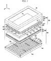
- FIG. 1is a prospective view of a liquid crystal display (LCD) device in accordance with exemplary embodiments
- FIG. 2is a block diagram of the LCD device of FIG. 1 in accordance with exemplary embodiments
- FIG. 3is an equivalent circuit diagram for a pixel in the LCD device of FIG. 2 in accordance with exemplary embodiments
- FIG. 4is a circuit diagram of an inverter portion of FIG. 1 in accordance with exemplary embodiments
- FIG. 5Ais a graphical view of results of comparing a conventional light source portion and the light source portion of FIG. 4 based on varying electric currents applied and with respect to varying times in accordance with exemplary embodiments;
- FIG. 5Bis a graphical view of results of comparing a conventional light source portion and the light source portion of FIG. 4 based on varying temperatures associated therewith and with respect to varying times in accordance with exemplary embodiments;
- FIG. 5Cis a graphical view of results of comparing a conventional light source portion and the light source portion of FIG. 4 based on varying levels of brightness and with respect to varying times in accordance with exemplary embodiments.
- FIG. 1is a prospective view of a liquid crystal display (LCD) device in accordance with exemplary embodiments
- FIG. 2is a block diagram of the LCD device of FIG. 1 in accordance with exemplary embodiments
- FIG. 3is an equivalent circuit diagram for a pixel in the LCD device of FIG. 2 in accordance with exemplary embodiments
- FIG. 4is a circuit diagram of an inverter portion of FIG. 1 in accordance with exemplary embodiments.
- a liquid crystal display (LCD) devicecomprises a display portion 330 , a backlight assembly 900 , upper and lower chassises 361 , 362 , respectively, and a mold frame 366 .
- the display portion 330comprises an LCD assembly 300 , multiple data and gate tape carrier packages (TCPs) 310 , 410 , respectively, that are attached to the LCD assembly 300 , and data and gate printed circuit boards (PCBs) 350 , 450 , respectively, attached to the corresponding data and gate TCPs 310 , 410 .
- TCPsdata and gate tape carrier packages
- PCBsdata and gate printed circuit boards
- the LCD assembly 300comprises lower and upper display substrates 100 , 200 , respectively, and a liquid crystal layer 3 disposed between the lower and upper display substrates 100 , 200 .
- the lower display substrate 100comprises multiple display signal lines (e.g., gate and data lines G 1 -G n , D 1 -D m ).
- a pixel 1000 in the LCD devicecomprises a switching element Q connected to each of the gate lines G 1 -G n and each of data lines D 1 -D m , a liquid crystal capacitor C lc , and optionally a storage capacitor C st .
- Multiple switching elements Qare formed on the lower display substrate 100 and each of the multiple switching elements Q has three terminals (e.g., gate, drain, and source electrodes).
- the liquid crystal capacitor C lcrepresents a capacitor that the liquid crystal layer 3 is disposed between a pixel electrode 190 and a common electrode 270 .
- the common electrode 270is formed on an upper substrate 200 , but may be formed on the lower display substrate 100 .
- the storage capacitor C strepresents a capacitor where a separate signal line (not shown) formed on the lower display substrate 100 overlaps the pixel electrode 190 . Further, the storage capacitor C st may form a capacitor where the pixel electrode 190 overlaps a previous gate line.
- a polarizer(not shown) may be attached to one surface of at least one lower and upper display substrates 100 , 200 .
- a color filter 230comprises red, blue, and green filters and faces the lower display substrate 100 . Further, the color filter 230 may be formed on the lower display substrate 100 .
- the LCD devicecomprises multiple pixels 1000 .
- the gate TCPs 410are attached to one or both edges of the lower display substrate 100 and have gate driving integrated circuits (gate ICs) 411 to 414 mounted thereon.
- the data TCPs 310are attached to one or both edges of the lower display substrate 100 and have data driving integrated circuits (data ICs) 311 to 316 mounted thereon.
- the gate PCB 450are attached to the gate TCPs 410 parallel to the lower display substrate 100 and the data PCB 350 are attached to the data TCPs 310 parallel to the lower display substrate 100 .
- the gamma voltage portion 800includes two groups of gamma voltages, such as one group has higher voltages and another group has lower voltages than a common voltage, for example. The number of the gamma voltages provided may be adjustable based on the resolution of the LCD device.
- gate and data drive portions 400 , 500are electrically connected to the gate and data lines G 1 -G n , D 1 -D m of the LCD assembly 300 over signal lines (not shown) formed on the data and gate TCPs 310 , 410 of FIG. 1 .
- the gate drive portion 400applies gate ON/OFF signals being a combination of Von and Voff signals to the gate lines G 1 -G n and the data drive portion 500 applies data signals DAT to the data lines D 1 -D m .
- the data and gate ICs 311 to 316 , 411 to 414may be mounted on the lower display substrate 100 , and may be also formed on the lower display substrate 100 using, e.g., TFT processes without having to mount the data and gate ICs 311 to 316 , 411 to 414 .
- the backlight assembly 900comprises a light source portion 960 mounted in the lower chassis 362 , an optical portion 910 disposed between the LCD assembly 300 and the light source portion 960 that adjusts light emitted from the light source portion 960 .
- the inverter portion 920controls the operation of the light source portion 960 .
- the light source portion 960comprises multiple lamps (LPs) such as fluorescent lamps, for example, multiple lamp holders 365 affixing the multiple LPs at both edges of the lower chassis 362 , multiple lamp supporters 364 , a reflect sheet 363 mounted under the multiple LPs and reflecting light from the multiple LPs toward the LCD assembly 300 .
- the multiple LPsmay comprise cold cathode fluorescent lamps (CCFLs), external electrode fluorescent lamps (EEFLs), light emitting diodes (LEDs), and a planar surface light source, for example.
- the number of the multiple LPsis not limited, but may be increased and reduced based on the size of the LCD device.
- the inverter portion 920comprises a first brightness control portion 921 , a second brightness control portion 922 , a temperature sensor 923 , a signal output portion 924 connected to the first and second brightness control portions 921 , 922 and the temperature sensor 923 , an inverter controller 925 connected to the signal output portion 924 , a switching portion 926 connected to the inverter controller 925 , a transforming portion 927 connected to the switching portion 926 and the light source portion 960 , and an electric current sensor 928 connected to the signal output portion 924 .
- the inverter portion 920may be mounted on an inverter PCB (not shown) and on the data and gate PCB 350 , 450 .
- the temperature sensor 923is mounted on the inverter portion 920 ; however, it will be understood that the temperature sensor 923 may be mounted on other suitable devices.
- the optical portion 910is disposed between the LCD assembly 300 and the light source portion 960 and comprises multiple optical sheets 901 and a diffusing sheet 902 diffusing light from the light source portion 960 toward the LCD assembly 300 .
- the multiple LPs of the light source portion 960are mounted under the lower display substrate 100 ; however, it will be understood that the multiple LPs may be mounted at one or both edges of the LCD assembly 300 .
- a light guide sheet(not shown) may be used instead of the diffusing sheet 902 .
- upper and lower casesmay be mounted at the upper portion of the upper chassis 361 and the lower portion of the lower chassis 362 , respectively.
- a signal controller 600controls the operation of the gate and data drive portions 400 , 500 .
- the signal controller 600receives input control signals (Vsync, Hsync, Mclk, DE) from an external source (e.g. a graphic controller)(not shown) and input image signals (R, G, B) and generates image signals (R′, G′, B′), gate control signals CONT 1 , and data control signals CONT 2 with respect to the input control signals (Vsync, Hsync, Mclk, DE) and the input image signals (R′, G′, B′).
- an external sourcee.g. a graphic controller
- the signal controller 600sends the gate control signals CONT 1 to the gate drive portion 400 and the data control signals CONT 2 to the data drive portion 500 .
- the gate control signals CONT 1include STV indicating start of one frame, CPV controlling an output timing of the gate on signal, OE indicating an ending time of one horizontal line, etc.
- the data control signals CONT 2include STH indicating start of one horizontal line, TP or LOAD instructing an output of data voltages, RVS or POL instructing polarity reverse of data voltages with respect to a common voltage, etc.
- the data drive portion 500receives the image signals (R′, G′, B′) from the signal controller 600 and outputs the data voltages by selecting gamma voltages corresponding to the image signals (R′, G′, B′) according to the data control signals CONT 2 .
- the gate drive portion 400applies the gate on signal according to the gate control signals CONT 1 to the gate lines and turns on the switching elements Q connected to the gate lines.
- the gate driving portion 400applies the gate-on voltage Von to the gate lines G 1 -G n according to the gate control signals CONT 1 from the signal controller 600 and turns on the switching elements Q connected to the gate lines G 1 -G n .
- the image data voltages applied to the data lines D 1 -D mare then applied to the corresponding pixels as the switching elements Q are turned on.
- the inverter portion 920converts DC voltages applied from an external source into AC voltages and applies the AC voltages to the light source portion 960 .
- the inverter portion 920turns on and off the light source portion 960 and controls the brightness of the light source portion 960 . Additionally, the inverter portion 920 controls the operation of the light source portion 960 based on temperature sense signals applied from the temperature sensor 923 .
- the first brightness control portion 921comprises a resistor R 11 connected to a power supply V cc , a resistor R 12 commonly connected to the resistor R 11 and an input terminal of the first brightness control signal DM 1 , a resistor R 13 connected to the power supply V cc , a transistor Q 11 , a resistor R 14 connected to a collector terminal of the transistor Q 11 , and a capacitor C 11 disposed between the resistor R 14 and a ground.
- a base terminal of the transistor Q 11is connected to the resistor R 12 , and an emitter terminal of the transistor Q 11 is connected to the ground.
- the second brightness control portion 922comprises a resistor R 21 connected to the power supply V cc , a resistor R 22 commonly connected to the resistor R 21 and an input terminal of the second brightness control signal DM 2 , a resistor R 23 disposed between the resistor R 22 and the ground, a transistor Q 21 having the base terminal connected to the resistor R 22 , and a resistor R 24 disposed between an emitter terminal of the transistor Q 21 and the ground.
- the temperature sensor 923comprises a temperature sensing part TH 31 and a resistor R 31 in series disposed between the power supply V cc and the ground, a capacitor C 31 disposed between the ground and the common terminal of the temperature sensing part TH 31 and the resistor R 31 , resistors R 32 , R 33 in series disposed between the power supply V cc and the ground, a capacitor C 32 disposed between the common terminal of the resistors R 32 , R 33 and the ground, a resistor R 34 connected to the common terminal of the temperature sensing part TH 31 and the resistor R 31 , an operational amplifier (OP-AMP) COM 31 that a negative terminal ( ⁇ ) is connected to the common terminal of the resistors R 32 , R 33 and a positive terminal (+) is connected to the resistor R 34 , and a resistor R 35 disposed between the positive terminal (+) and the output terminal of the OP-AMP COM 31 .
- OP-AMPoperational amplifier
- the signal output portion 924comprises diodes D 41 , D 42 forwardly connected to the capacitor C 11 of the first brightness control portion 921 , diode D 43 forwardly connected to a collector terminal of the transistor Q 21 of the second brightness control portion 922 , and a resistor R 41 connected to the output terminal of the OP-AMP COM 31 of the temperature sensor 923 and the diodes D 42 , D 43 .
- the electric current sensor 928comprises a resistor R 51 connected to the light source portion 960 and the resistor R 42 of the signal output portion 924 .
- the temperature sensing part TH 31 of the temperature sensor 923comprises a thermistor that is a temperature sensing element having varying resistance based on a sensed temperature, for example.
- the resistance of the thermistor used as the temperature sensing part TH 31is reduced as the sensed temperature increases. Conversely, the resistance of the thermistor used as the temperature sensing part TH 31 is increased as the sensed temperature is reduced.
- the temperature sensing part TH 31may be mounted on the multiple LPs of the light source portion 960 or a certain position representing a temperature substantially similar to the multiple LPs. However, the operation or the position of the temperature sensing part TH 31 may vary based on the characteristics of the LCD device.
- the inverter portion 920may control an electric current of the multiple LPs of the light source portion 960 based on the sensed temperature from the temperature sensing part TH 31 and prevent reduction of the brightness of the multiple LPs caused by reduction of the temperature.
- a triangular wave of the initial frequency applied from an external source (e.g., an oscillating portion)(not shown)is generated, and a pulse width modulation (PWM) signal based on an initial DC level of a control signal applied from an external source (not shown) is then applied to the first brightness control portion 921 as a first brightness control signal DM 1 .
- PWMpulse width modulation
- a high level of the first brightness control signal DM 1refers to a Turn-On period of the multiple LPs of the light source portion 960 and a low level of the first brightness control signal DM 1 refers to a Turn-Off period of the multiple LPs of the light source portion 960 .
- the first brightness control signal DM 1may change a duty ratio of the control signal as a user adjusts the DC level of the control signal applied from the external source (not shown) using a control switch (not shown), for example, and thus change the Turn-On and Turn-Off cycle of the light source portion 960 .
- the first brightness control portion 921applies the first brightness control signal DM 1 to the transistor Q 11 through the resistor R 12 .
- the transistor Q 11is turned on or off based on the first brightness control signal DM 1 , and an inverted phase signal with respect to the first brightness control signal DM 1 is applied to the signal output portion 924 through the resistor R 14 and the capacitor C 11 .
- the resistor R 11may be, e.g., a pull-up resistor.
- the second brightness control portion 922adjusts the second brightness control signal DM 2 to a desired level using the resistors R 22 , R 23 , and applies the adjusted level of the second brightness control signal DM 2 to the transistor Q 21 .
- the second brightness control signal DM 2is a desired DC level of signal and may adjust the desired DC level of the signal based on brightness of the light source portion 960 .
- the transistor Q 21 and the resistor R 24operate as an emitter follower.
- a voltage of the emitter terminal of the transistor Q 21is set by the second brightness control signal DM 2 , and when the transistor Q 21 operates, an electric current applied to the collector terminal of the transistor Q 21 flows into the ground through the resistor R 24 .
- the resistor R 21may be, e.g., a pull-up resistor.
- the temperature sensor 923operates based on the temperature sensed by the temperature sensing part TH 31 . For example, if the resistance of the temperature sensing part TH 31 based on the sensed temperature is set, the power supply V cc is divided by the temperature sensing part TH 31 and the resistor R 31 to a corresponding voltage level, and the divided voltage level is then applied to the positive terminal (+) of the OP-AMP COM 31 through the resistor R 34 .
- the power supply V ccis divided by the resistors R 32 , R 33 to a corresponding voltage level and the divided voltage level is then applied to the negative terminal ( ⁇ ) of the OP-AMP COM 31 through the resistor R 34 .
- the OP-AMP COM 31operates as a comparator and the divided voltage by the resistors R 32 , R 33 is used as a reference voltage of the OP-AMP COM 31 .
- a voltage level at an output terminal of the OP-AMP COM 31is set based on the magnitude of the voltages applied to the negative ( ⁇ ) and positive (+) terminals of the OP-AMP COM 31 .
- the voltage applied to the positive terminal (+) of the OP-AMP COM 31receives less than the reference voltage applied to the negative terminal ( ⁇ ) of the OP-AMP COM 31 . Therefore, the output voltage of the OP-AMP COM 31 becomes a low level of voltage.
- the resistor R 34comprises adjusting difference of the signals caused by difference of the resistances between the temperature sensing part TH 31 and the resistor R 31 and difference of the -resistances between the resistors R 32 , R 33 .
- the OP-AMP COM 31may have characteristics of hysteresis by the resistor R 35 . Therefore, since a switching point of the output voltage of the OP-AMP COM 31 from a high level to a low level and from a low level to a high level is not the same, the OP-AMP COM 31 may reduce noise caused by frequent variation of the signals.
- the predetermined temperatureis about ⁇ 10° C. that cannot operate normally, in the embodiment, the predetermined temperature may be adjustable based on the operational characteristics of the multiple LPs or the surrounding circumstance of the LCD device.
- the inverter controller 925turns on or turns off the light source portion 960 based on a feedback signal applied from the electric current sensor 928 .
- the inverter controller 925generates the control signal of a desired frequency for an initial operation of the light source portion 960 and applies the control signal of the desired frequency to the switching portion 926 .
- the control signal generated from the inverter controller 925may apply a maximum driving voltage to the light source portion 960 .
- the switching portion 926responds to the control signal applied from the inverter controller 925 by converting a DC voltage from an external source (not shown) into an AC voltage and applying the AC voltage to the transforming portion 927 .
- the transforming portion 927ramps up the AC voltage applied from the switching portion 923 to a higher voltage based on a winding ratio and applies the ramped-up voltage to the light source portion 960 , thus, the multiple LPs of the light source portion 960 are turned on.
- the electric current sensor 928applies a voltage proportional to the electric current of the multiple LPs of the light source portion 960 using the resistor R 41 to the signal output portion 924 .
- the voltage applied from the electric current sensor 928is delivered to the resistor R 24 through the transistor Q 21 of the second brightness control portion 922 . Since the output voltage of the OP-AMP COM 31 is a low level, the voltage applied from the electric current sensor 928 is delivered to the temperature sensor 923 through the diode D 43 and the resistor R 41 of the signal output portion 924 , and the voltage applied from the temperature sensor 923 is delivered to the inverter controller 925 through the resistor R 42 .
- the inverter controller 925adjusts a driving voltage to be applied to the light source portion 960 based on a control signal of the electric current sensor 928 caused by the feedback through the resistor R 42 , and makes the electric current of the multiple LPs of the light source portion 960 uniform.
- the output voltage of the OP-AMP COM 31 of the temperature sensor 923is a low level
- the voltage of the control signal output from the electric current sensor 928is delivered to the temperature sensor 923 , as well as the inverter controller 925 and the second brightness control portion 922 . Therefore, the voltage of the control signal applied to the inverter controller 925 is reduced by a voltage divided by the resistor R 42 . To compensate for the reduced voltage, the inverter controller 925 increases the driving voltage for the light source portion 960 .
- the voltage of the control signal applied to the inverter controller 925becomes a low level through the diode D 41 and the voltage of the control signal caused by the feedback through the resistor R 42 is lowered. Amounts of the electric current of the light source portion 960 may be increased by increasing the driving voltage for the light source portion 960 while continuously turning on the light source portion 960 .
- the voltage applied to the positive terminal (+) of the OP-AMP COM 31 through the temperature sensing part TH 31 and the resistor R 31becomes more than the reference voltage of the OP-AMP COM 31 and thus the OP-AMP COM 31 outputs a voltage higher than the reference voltage. Therefore, the output signal applied from the first brightness control portion 921 is inverted through the diode D 41 of the signal output portion 924 , and the inverted output signal is applied to the inverter controller 925 .
- the voltage applied from the electric current sensor 928is delivered to the resistor R 24 through the transistor Q 21 of the second brightness control portion 922 and applied to the inverter controller 925 through the resistor R 42 .
- the inverter controller 925controls operation of the switching portion 926 for making amounts of the electric current of the multiple LPs of the light source portion 960 uniform during a high level of the first brightness control signal DM 1 . In this way, when the surrounding temperature of the temperature sensing part TH 31 is more than the predetermined temperature of the LCD device, the inverter controller 925 turns on or turns off the light source portion 960 based on the first brightness control signal DM 1 and the feedback signal applied from the electric current sensor 928 .
- Varying electric currents, varying temperatures, and varying brightness of the multiple LPs of the light source portion 960 with respect to varying timeswill be now described with reference to FIGS. 5A to 5C .
- FIG. 5Ais a graphical view of results of comparing a conventional light source portion and the light source portion of FIG. 4 based on varying electric currents applied and with respect to varying times
- FIG. 5Bis a graphical view of results of comparing a conventional light source portion and the light source portion of FIG. 4 based on varying temperatures associated therewith and with respect to varying times
- FIG. 5Cis a graphical view of results of comparing a conventional light source portion and the light source portion of FIG. 4 based on varying levels of brightness and with respect to varying times.
- the electric current of the multiple LPs of the light source portion 960is ramped up and is maintained, e.g., at a maximum of electric current (“A”) until the surrounding temperature of the light source portion 960 becomes more than the predetermined temperature of the LCD device.
- Amaximum of electric current
- the conventional multiple LPsmaintain a constant electric current (“A′”) regardless of the varying times.
- the time (“B”) in which an operational temperature (e.g., 10° C.) of the multiple LPs of the light source portion 960 is reachedis faster than that of the conventional multiple LPs (“B′”).
- an operational temperaturee.g. 10° C.
- the time (“C”)the desired brightness level of the light source portion 960 is reached more quickly than that of the conventional multiple LPs (“C′”).
- the driving voltage applied to the light source portionbecomes a maximum of voltage and thus a maximum of electric current is applied to the multiple LPs of the light source portion.
- the time for which the surrounding temperature of the light source portion reaches an operational temperaturemay be shortened, thus, preventing any reduction of the brightness of the light source portion caused by mal-functional operation of the discharging gases.
- the light source portionoperates at the predetermined temperature of the LCD device, erosion of the electrodes of the multiple LPs caused by the discharging gases may be prevented and reduction of the life span of the light source portion may be prevented.
Landscapes
- Physics & Mathematics (AREA)
- Engineering & Computer Science (AREA)
- General Physics & Mathematics (AREA)
- Theoretical Computer Science (AREA)
- Computer Hardware Design (AREA)
- Nonlinear Science (AREA)
- Crystallography & Structural Chemistry (AREA)
- Optics & Photonics (AREA)
- Chemical & Material Sciences (AREA)
- Mathematical Physics (AREA)
- Liquid Crystal (AREA)
- Liquid Crystal Display Device Control (AREA)
- Control Of Indicators Other Than Cathode Ray Tubes (AREA)
- Circuit Arrangements For Discharge Lamps (AREA)
- Planar Illumination Modules (AREA)
Abstract
Description
Claims (19)
Applications Claiming Priority (2)
| Application Number | Priority Date | Filing Date | Title |
|---|---|---|---|
| KR10-2004-0057127 | 2004-07-22 | ||
| KR1020040057127AKR101133755B1 (en) | 2004-07-22 | 2004-07-22 | Display device and driving device of light source for display device |
Publications (2)
| Publication Number | Publication Date |
|---|---|
| US20060017404A1 US20060017404A1 (en) | 2006-01-26 |
| US7595785B2true US7595785B2 (en) | 2009-09-29 |
Family
ID=35656430
Family Applications (1)
| Application Number | Title | Priority Date | Filing Date |
|---|---|---|---|
| US11/187,480Expired - Fee RelatedUS7595785B2 (en) | 2004-07-22 | 2005-07-22 | Display device and driving device for a light source |
Country Status (5)
| Country | Link |
|---|---|
| US (1) | US7595785B2 (en) |
| JP (1) | JP2006039558A (en) |
| KR (1) | KR101133755B1 (en) |
| CN (1) | CN100578302C (en) |
| TW (1) | TW200604676A (en) |
Cited By (26)
| Publication number | Priority date | Publication date | Assignee | Title |
|---|---|---|---|---|
| US20070176885A1 (en)* | 2006-02-02 | 2007-08-02 | Samsung Electronics Co., Ltd | Back light unit having a plurality of luminous elements and control method thereof |
| US20080272798A1 (en)* | 2007-05-01 | 2008-11-06 | Funai Electric Co., Ltd. | Display device and liquid crystal television |
| US20090289580A1 (en)* | 2008-05-21 | 2009-11-26 | Manufacturing Resources International, Inc. | Backlight adjustment system |
| US20110109655A1 (en)* | 2008-08-08 | 2011-05-12 | Daisuke Takeda | Backlight and display device using the same |
| US9799306B2 (en) | 2011-09-23 | 2017-10-24 | Manufacturing Resources International, Inc. | System and method for environmental adaptation of display characteristics |
| US9812047B2 (en) | 2010-02-25 | 2017-11-07 | Manufacturing Resources International, Inc. | System and method for remotely monitoring the operating life of electronic displays |
| US9924583B2 (en) | 2015-05-14 | 2018-03-20 | Mnaufacturing Resources International, Inc. | Display brightness control based on location data |
| US10353785B2 (en) | 2015-09-10 | 2019-07-16 | Manufacturing Resources International, Inc. | System and method for systemic detection of display errors |
| US10578658B2 (en) | 2018-05-07 | 2020-03-03 | Manufacturing Resources International, Inc. | System and method for measuring power consumption of an electronic display assembly |
| US10586508B2 (en) | 2016-07-08 | 2020-03-10 | Manufacturing Resources International, Inc. | Controlling display brightness based on image capture device data |
| US10593255B2 (en) | 2015-05-14 | 2020-03-17 | Manufacturing Resources International, Inc. | Electronic display with environmental adaptation of display characteristics based on location |
| US10607520B2 (en) | 2015-05-14 | 2020-03-31 | Manufacturing Resources International, Inc. | Method for environmental adaptation of display characteristics based on location |
| US10782276B2 (en) | 2018-06-14 | 2020-09-22 | Manufacturing Resources International, Inc. | System and method for detecting gas recirculation or airway occlusion |
| US10908863B2 (en) | 2018-07-12 | 2021-02-02 | Manufacturing Resources International, Inc. | System and method for providing access to co-located operations data for an electronic display |
| US11137847B2 (en) | 2019-02-25 | 2021-10-05 | Manufacturing Resources International, Inc. | Monitoring the status of a touchscreen |
| US11398181B2 (en)* | 2020-01-03 | 2022-07-26 | Samsung Electronics Co., Ltd. | Display module and driving method thereof |
| US11402940B2 (en) | 2019-02-25 | 2022-08-02 | Manufacturing Resources International, Inc. | Monitoring the status of a touchscreen |
| US11526044B2 (en) | 2020-03-27 | 2022-12-13 | Manufacturing Resources International, Inc. | Display unit with orientation based operation |
| US11921010B2 (en) | 2021-07-28 | 2024-03-05 | Manufacturing Resources International, Inc. | Display assemblies with differential pressure sensors |
| US11965804B2 (en) | 2021-07-28 | 2024-04-23 | Manufacturing Resources International, Inc. | Display assemblies with differential pressure sensors |
| US11972672B1 (en) | 2022-10-26 | 2024-04-30 | Manufacturing Resources International, Inc. | Display assemblies providing open and unlatched alerts, systems and methods for the same |
| US11989476B2 (en) | 2018-07-12 | 2024-05-21 | Manufacturing Resources International, Inc. | Systems and methods for remotely monitoring electronic displays |
| US12022635B2 (en) | 2021-03-15 | 2024-06-25 | Manufacturing Resources International, Inc. | Fan control for electronic display assemblies |
| US12027132B1 (en) | 2023-06-27 | 2024-07-02 | Manufacturing Resources International, Inc. | Display units with automated power governing |
| US12105370B2 (en) | 2021-03-15 | 2024-10-01 | Manufacturing Resources International, Inc. | Fan control for electronic display assemblies |
| US12393241B1 (en) | 2024-04-04 | 2025-08-19 | Manufacturing Resources International, Inc. | Display assembly using air characteristic data to verify display assembly operating conditions, systems and methods for the same |
Families Citing this family (16)
| Publication number | Priority date | Publication date | Assignee | Title |
|---|---|---|---|---|
| KR100735460B1 (en)* | 2005-09-09 | 2007-07-03 | 삼성전기주식회사 | LED drive control circuit with temperature compensation |
| JP4830436B2 (en)* | 2005-10-03 | 2011-12-07 | 株式会社日立製作所 | Display device |
| US20070132709A1 (en)* | 2005-12-12 | 2007-06-14 | Toshiba Matsushita Display Technology Co., Ltd | Liquid crystal display device and method for driving the same |
| CN100446631C (en)* | 2006-04-30 | 2008-12-24 | 友达光电股份有限公司 | Brightness adjusting circuit and electroluminescent display using the same |
| JP4207986B2 (en)* | 2006-06-28 | 2009-01-14 | 双葉電子工業株式会社 | Fluorescent display device and driving method thereof |
| KR20080033771A (en)* | 2006-10-13 | 2008-04-17 | 삼성전자주식회사 | Driving device of backlight unit, liquid crystal display device having same, and control method thereof |
| EP1926351B1 (en)* | 2006-11-08 | 2012-12-19 | MathBright Technology Co., Ltd. | Driving circuit of surface light source and method of driving the same |
| JP5134237B2 (en)* | 2006-12-13 | 2013-01-30 | エルジー ディスプレイ カンパニー リミテッド | Liquid crystal display |
| JP2008251339A (en) | 2007-03-30 | 2008-10-16 | Sony Corp | Fluorescent tube driving method, and its device |
| KR101577818B1 (en)* | 2007-04-09 | 2015-12-15 | 주식회사 엘지씨엔에스 | Apparatus and method for detector of media thickness |
| TWI383367B (en)* | 2008-06-13 | 2013-01-21 | Hon Hai Prec Ind Co Ltd | Display driving circuit |
| TWI408650B (en)* | 2008-07-10 | 2013-09-11 | Innolux Corp | Display, driving apparatus and driving method thereof |
| CN102135931A (en)* | 2010-01-25 | 2011-07-27 | 英业达股份有限公司 | Test module of passive backboard and method for testing passive backboard |
| JP5400667B2 (en)* | 2010-03-10 | 2014-01-29 | 富士重工業株式会社 | Driving device for field emission lamp |
| US9459141B2 (en)* | 2014-03-11 | 2016-10-04 | Getac Technology Corporation | Brightness control apparatus and brightness control method |
| EP4171954A1 (en)* | 2020-06-25 | 2023-05-03 | Saint-Gobain Glass France | Method for electrically controlling a functional element |
Citations (28)
| Publication number | Priority date | Publication date | Assignee | Title |
|---|---|---|---|---|
| JPH07211468A (en) | 1994-01-18 | 1995-08-11 | Ushio Inc | Small fluorescent tube lighting device |
| JPH07272881A (en) | 1994-03-31 | 1995-10-20 | Toshiba Lighting & Technol Corp | Discharge lamp lighting device and lighting device |
| JPH10104571A (en) | 1996-09-30 | 1998-04-24 | Sharp Corp | Liquid crystal display |
| JPH10148808A (en) | 1996-11-18 | 1998-06-02 | Seiko Epson Corp | Backlight device and liquid crystal display device using the same |
| JPH10189259A (en) | 1996-12-19 | 1998-07-21 | Nec Home Electron Ltd | Dimming device for backlight |
| US5907742A (en) | 1997-03-09 | 1999-05-25 | Hewlett-Packard Company | Lamp control scheme for rapid warmup of fluorescent lamp in office equipment |
| US6066920A (en) | 1997-01-07 | 2000-05-23 | Sharp Kabushiki Kaisha | Illumination device, method for driving the illumination device and display including the illumination device |
| JP2000150191A (en) | 1998-11-13 | 2000-05-30 | Murata Mfg Co Ltd | Cold cathode tube drive |
| US6198234B1 (en)* | 1999-06-09 | 2001-03-06 | Linfinity Microelectronics | Dimmable backlight system |
| JP2001169273A (en) | 1999-12-06 | 2001-06-22 | Sharp Corp | Color television door phone |
| US6288388B1 (en)* | 1997-09-26 | 2001-09-11 | Semiconductor Energy Laboratory Co., Ltd. | Photoelectric converter wherein the lower electrode has bends |
| KR20020017358A (en) | 2000-08-30 | 2002-03-07 | 강웅현 | Inverter drive apparatus for back light of liquid crystal display |
| US6388388B1 (en)* | 2000-12-27 | 2002-05-14 | Visteon Global Technologies, Inc. | Brightness control system and method for a backlight display device using backlight efficiency |
| US20020109467A1 (en)* | 2001-02-13 | 2002-08-15 | Koito Manufacturing Co., Ltd. | Discharge-lamp lighting circuit |
| US20020130786A1 (en)* | 2001-01-16 | 2002-09-19 | Visteon Global Technologies,Inc. | Series led backlight control circuit |
| JP2002311413A (en) | 2001-04-18 | 2002-10-23 | Totoku Electric Co Ltd | Luminance control method for liquid crystal display device, luminance control device, and liquid crystal display device |
| KR100361192B1 (en) | 1999-03-30 | 2002-11-18 | 가부시끼가이샤 무라따 세이사꾸쇼 | Control apparatus capable of improving a rise time characteristic of a light source |
| US20030011326A1 (en)* | 2001-07-13 | 2003-01-16 | Noh Shi Youl | Fluorescent lamp brightness controller |
| JP2003045693A (en) | 2001-07-11 | 2003-02-14 | Fiirakkusu Corporated | Fluorescent lamp brightness adjusting device |
| US20030043106A1 (en)* | 2001-08-30 | 2003-03-06 | Lg Electronics Inc. | Lamp drive apparatus and drive method of a notebook computer |
| KR20030084451A (en) | 2002-04-26 | 2003-11-01 | 코츠테크놀로지주식회사 | Back Light Unit for LCD Device |
| KR20040006304A (en) | 2002-07-11 | 2004-01-24 | 엘지전자 주식회사 | stabilization device of luminance for LCD and the method of control |
| US6713744B1 (en) | 1999-10-28 | 2004-03-30 | Nec Corporation | Scanner having cold-cathode-tube light source and method of controlling a drive signal for illuminating a cold-cathode-tube light source |
| CN1499248A (en) | 2002-09-04 | 2004-05-26 | ���ǵ�����ʽ���� | Inverter for LCD |
| US20040130521A1 (en)* | 2003-01-04 | 2004-07-08 | Samsung Electronics Co., Ltd. | Display apparatus and method |
| US20040246226A1 (en)* | 2003-05-23 | 2004-12-09 | Seung-Hwan Moon | Inverter and liquid crystal display including inverter |
| US7075596B2 (en)* | 2001-08-01 | 2006-07-11 | Sanyo Electric Co., Ltd. | Liquid crystal projector |
| US7183727B2 (en)* | 2003-09-23 | 2007-02-27 | Microsemi Corporation | Optical and temperature feedbacks to control display brightness |
- 2004
- 2004-07-22KRKR1020040057127Apatent/KR101133755B1/ennot_activeExpired - Fee Related
- 2005
- 2005-06-28TWTW094121613Apatent/TW200604676A/enunknown
- 2005-07-22JPJP2005213452Apatent/JP2006039558A/ennot_activeWithdrawn
- 2005-07-22USUS11/187,480patent/US7595785B2/ennot_activeExpired - Fee Related
- 2005-07-22CNCN200510087421Apatent/CN100578302C/ennot_activeExpired - Fee Related
Patent Citations (28)
| Publication number | Priority date | Publication date | Assignee | Title |
|---|---|---|---|---|
| JPH07211468A (en) | 1994-01-18 | 1995-08-11 | Ushio Inc | Small fluorescent tube lighting device |
| JPH07272881A (en) | 1994-03-31 | 1995-10-20 | Toshiba Lighting & Technol Corp | Discharge lamp lighting device and lighting device |
| JPH10104571A (en) | 1996-09-30 | 1998-04-24 | Sharp Corp | Liquid crystal display |
| JPH10148808A (en) | 1996-11-18 | 1998-06-02 | Seiko Epson Corp | Backlight device and liquid crystal display device using the same |
| JPH10189259A (en) | 1996-12-19 | 1998-07-21 | Nec Home Electron Ltd | Dimming device for backlight |
| US6066920A (en) | 1997-01-07 | 2000-05-23 | Sharp Kabushiki Kaisha | Illumination device, method for driving the illumination device and display including the illumination device |
| US5907742A (en) | 1997-03-09 | 1999-05-25 | Hewlett-Packard Company | Lamp control scheme for rapid warmup of fluorescent lamp in office equipment |
| US6288388B1 (en)* | 1997-09-26 | 2001-09-11 | Semiconductor Energy Laboratory Co., Ltd. | Photoelectric converter wherein the lower electrode has bends |
| JP2000150191A (en) | 1998-11-13 | 2000-05-30 | Murata Mfg Co Ltd | Cold cathode tube drive |
| KR100361192B1 (en) | 1999-03-30 | 2002-11-18 | 가부시끼가이샤 무라따 세이사꾸쇼 | Control apparatus capable of improving a rise time characteristic of a light source |
| US6198234B1 (en)* | 1999-06-09 | 2001-03-06 | Linfinity Microelectronics | Dimmable backlight system |
| US6713744B1 (en) | 1999-10-28 | 2004-03-30 | Nec Corporation | Scanner having cold-cathode-tube light source and method of controlling a drive signal for illuminating a cold-cathode-tube light source |
| JP2001169273A (en) | 1999-12-06 | 2001-06-22 | Sharp Corp | Color television door phone |
| KR20020017358A (en) | 2000-08-30 | 2002-03-07 | 강웅현 | Inverter drive apparatus for back light of liquid crystal display |
| US6388388B1 (en)* | 2000-12-27 | 2002-05-14 | Visteon Global Technologies, Inc. | Brightness control system and method for a backlight display device using backlight efficiency |
| US20020130786A1 (en)* | 2001-01-16 | 2002-09-19 | Visteon Global Technologies,Inc. | Series led backlight control circuit |
| US20020109467A1 (en)* | 2001-02-13 | 2002-08-15 | Koito Manufacturing Co., Ltd. | Discharge-lamp lighting circuit |
| JP2002311413A (en) | 2001-04-18 | 2002-10-23 | Totoku Electric Co Ltd | Luminance control method for liquid crystal display device, luminance control device, and liquid crystal display device |
| JP2003045693A (en) | 2001-07-11 | 2003-02-14 | Fiirakkusu Corporated | Fluorescent lamp brightness adjusting device |
| US20030011326A1 (en)* | 2001-07-13 | 2003-01-16 | Noh Shi Youl | Fluorescent lamp brightness controller |
| US7075596B2 (en)* | 2001-08-01 | 2006-07-11 | Sanyo Electric Co., Ltd. | Liquid crystal projector |
| US20030043106A1 (en)* | 2001-08-30 | 2003-03-06 | Lg Electronics Inc. | Lamp drive apparatus and drive method of a notebook computer |
| KR20030084451A (en) | 2002-04-26 | 2003-11-01 | 코츠테크놀로지주식회사 | Back Light Unit for LCD Device |
| KR20040006304A (en) | 2002-07-11 | 2004-01-24 | 엘지전자 주식회사 | stabilization device of luminance for LCD and the method of control |
| CN1499248A (en) | 2002-09-04 | 2004-05-26 | ���ǵ�����ʽ���� | Inverter for LCD |
| US20040130521A1 (en)* | 2003-01-04 | 2004-07-08 | Samsung Electronics Co., Ltd. | Display apparatus and method |
| US20040246226A1 (en)* | 2003-05-23 | 2004-12-09 | Seung-Hwan Moon | Inverter and liquid crystal display including inverter |
| US7183727B2 (en)* | 2003-09-23 | 2007-02-27 | Microsemi Corporation | Optical and temperature feedbacks to control display brightness |
Cited By (66)
| Publication number | Priority date | Publication date | Assignee | Title |
|---|---|---|---|---|
| US20070176885A1 (en)* | 2006-02-02 | 2007-08-02 | Samsung Electronics Co., Ltd | Back light unit having a plurality of luminous elements and control method thereof |
| US7795821B2 (en)* | 2006-02-02 | 2010-09-14 | Samsung Electronics Co., Ltd. | Back light unit having a plurality of luminous elements and control method thereof |
| US7816908B2 (en)* | 2007-05-01 | 2010-10-19 | Funai Electric Co., Ltd. | Display device and liquid crystal television |
| US20080272798A1 (en)* | 2007-05-01 | 2008-11-06 | Funai Electric Co., Ltd. | Display device and liquid crystal television |
| US9030129B2 (en) | 2008-05-21 | 2015-05-12 | Manufacturing Resources International, Inc. | Backlight adjustment system |
| US8125163B2 (en)* | 2008-05-21 | 2012-02-28 | Manufacturing Resources International, Inc. | Backlight adjustment system |
| US8829815B2 (en) | 2008-05-21 | 2014-09-09 | Manufacturing Resources International, Inc. | Backlight adjustment system |
| US9167655B2 (en) | 2008-05-21 | 2015-10-20 | Manufacturing Resources International, Inc. | Backlight adjustment system |
| US9867253B2 (en) | 2008-05-21 | 2018-01-09 | Manufacturing Resources International, Inc. | Backlight adjustment system |
| US20090289580A1 (en)* | 2008-05-21 | 2009-11-26 | Manufacturing Resources International, Inc. | Backlight adjustment system |
| US10440790B2 (en) | 2008-05-21 | 2019-10-08 | Manufacturing Resources International, Inc. | Electronic display system with illumination control |
| US20110109655A1 (en)* | 2008-08-08 | 2011-05-12 | Daisuke Takeda | Backlight and display device using the same |
| US10325536B2 (en) | 2010-02-25 | 2019-06-18 | Manufacturing Resources International, Inc. | System and method for remotely monitoring and adjusting electronic displays |
| US9812047B2 (en) | 2010-02-25 | 2017-11-07 | Manufacturing Resources International, Inc. | System and method for remotely monitoring the operating life of electronic displays |
| US9799306B2 (en) | 2011-09-23 | 2017-10-24 | Manufacturing Resources International, Inc. | System and method for environmental adaptation of display characteristics |
| US10255884B2 (en) | 2011-09-23 | 2019-04-09 | Manufacturing Resources International, Inc. | System and method for environmental adaptation of display characteristics |
| US10412816B2 (en) | 2015-05-14 | 2019-09-10 | Manufacturing Resources International, Inc. | Display brightness control based on location data |
| US9924583B2 (en) | 2015-05-14 | 2018-03-20 | Mnaufacturing Resources International, Inc. | Display brightness control based on location data |
| US10607520B2 (en) | 2015-05-14 | 2020-03-31 | Manufacturing Resources International, Inc. | Method for environmental adaptation of display characteristics based on location |
| US10321549B2 (en) | 2015-05-14 | 2019-06-11 | Manufacturing Resources International, Inc. | Display brightness control based on location data |
| US10593255B2 (en) | 2015-05-14 | 2020-03-17 | Manufacturing Resources International, Inc. | Electronic display with environmental adaptation of display characteristics based on location |
| US10353785B2 (en) | 2015-09-10 | 2019-07-16 | Manufacturing Resources International, Inc. | System and method for systemic detection of display errors |
| US11093355B2 (en) | 2015-09-10 | 2021-08-17 | Manufacturing Resources International, Inc. | System and method for detection of display errors |
| US10586508B2 (en) | 2016-07-08 | 2020-03-10 | Manufacturing Resources International, Inc. | Controlling display brightness based on image capture device data |
| US10578658B2 (en) | 2018-05-07 | 2020-03-03 | Manufacturing Resources International, Inc. | System and method for measuring power consumption of an electronic display assembly |
| US11656255B2 (en) | 2018-05-07 | 2023-05-23 | Manufacturing Resources International, Inc. | Measuring power consumption of a display assembly |
| US11022635B2 (en) | 2018-05-07 | 2021-06-01 | Manufacturing Resources International, Inc. | Measuring power consumption of an electronic display assembly |
| US11774428B2 (en) | 2018-06-14 | 2023-10-03 | Manufacturing Resources International, Inc. | System and method for detecting gas recirculation or airway occlusion |
| US10782276B2 (en) | 2018-06-14 | 2020-09-22 | Manufacturing Resources International, Inc. | System and method for detecting gas recirculation or airway occlusion |
| US11977065B2 (en) | 2018-06-14 | 2024-05-07 | Manufacturing Resources International, Inc. | System and method for detecting gas recirculation or airway occlusion |
| US11293908B2 (en) | 2018-06-14 | 2022-04-05 | Manufacturing Resources International, Inc. | System and method for detecting gas recirculation or airway occlusion |
| US11243733B2 (en) | 2018-07-12 | 2022-02-08 | Manufacturing Resources International, Inc. | System and method for providing access to co-located operations data for an electronic display |
| US12169658B2 (en) | 2018-07-12 | 2024-12-17 | Manufacturing Resources International, Inc. | Systems and methods for remotely monitoring electronic displays |
| US11455138B2 (en) | 2018-07-12 | 2022-09-27 | Manufacturing Resources International, Inc. | System and method for providing access to co-located operations data for an electronic display |
| US11989476B2 (en) | 2018-07-12 | 2024-05-21 | Manufacturing Resources International, Inc. | Systems and methods for remotely monitoring electronic displays |
| US11614911B2 (en) | 2018-07-12 | 2023-03-28 | Manufacturing Resources International, Inc. | System and method for providing access to co-located operations data for an electronic display |
| US12333200B2 (en) | 2018-07-12 | 2025-06-17 | Manufacturing Resources International, Inc. | Systems and methods for remotely monitoring electronic displays |
| US10908863B2 (en) | 2018-07-12 | 2021-02-02 | Manufacturing Resources International, Inc. | System and method for providing access to co-located operations data for an electronic display |
| US11928380B2 (en) | 2018-07-12 | 2024-03-12 | Manufacturing Resources International, Inc. | System and method for providing access to co-located operations data for an electronic display |
| US11402940B2 (en) | 2019-02-25 | 2022-08-02 | Manufacturing Resources International, Inc. | Monitoring the status of a touchscreen |
| US11644921B2 (en) | 2019-02-25 | 2023-05-09 | Manufacturing Resources International, Inc. | Monitoring the status of a touchscreen |
| US11137847B2 (en) | 2019-02-25 | 2021-10-05 | Manufacturing Resources International, Inc. | Monitoring the status of a touchscreen |
| US12175035B2 (en) | 2019-02-25 | 2024-12-24 | Manufacturing Resources International, Inc. | Monitoring the status of a touchscreen |
| US11790836B2 (en) | 2020-01-03 | 2023-10-17 | Samsung Electronics Co., Ltd. | Display module and driving method thereof |
| US11398181B2 (en)* | 2020-01-03 | 2022-07-26 | Samsung Electronics Co., Ltd. | Display module and driving method thereof |
| US12117684B2 (en) | 2020-03-27 | 2024-10-15 | Manufacturing Resources International, Inc. | Display unit with orientation based operation |
| US11526044B2 (en) | 2020-03-27 | 2022-12-13 | Manufacturing Resources International, Inc. | Display unit with orientation based operation |
| US12007637B2 (en) | 2020-03-27 | 2024-06-11 | Manufacturing Resources International, Inc. | Display unit with orientation based operation |
| US12298614B2 (en) | 2020-03-27 | 2025-05-13 | Manufacturing Resources International, Inc. | Display unit with monitoring features |
| US12326626B2 (en) | 2020-03-27 | 2025-06-10 | Manufacturing Resources International, Inc. | Display unit with monitoring features |
| US11815755B2 (en) | 2020-03-27 | 2023-11-14 | Manufacturing Resources International, Inc. | Display unit with orientation based operation |
| US12416829B2 (en) | 2021-03-15 | 2025-09-16 | Manufacturing Resources International, Inc. | Display assemblies with condensation mitigation and related systems and methods |
| US12105370B2 (en) | 2021-03-15 | 2024-10-01 | Manufacturing Resources International, Inc. | Fan control for electronic display assemblies |
| US12245399B2 (en) | 2021-03-15 | 2025-03-04 | Manufacturing Resources International, Inc. | Fan control for electronic display assemblies |
| US12022635B2 (en) | 2021-03-15 | 2024-06-25 | Manufacturing Resources International, Inc. | Fan control for electronic display assemblies |
| US12321058B2 (en) | 2021-03-15 | 2025-06-03 | Manufacturing Resources International, Inc. | Display assemblies with condensation mitigation and related systems and methods |
| US11965804B2 (en) | 2021-07-28 | 2024-04-23 | Manufacturing Resources International, Inc. | Display assemblies with differential pressure sensors |
| US11921010B2 (en) | 2021-07-28 | 2024-03-05 | Manufacturing Resources International, Inc. | Display assemblies with differential pressure sensors |
| US12165489B2 (en) | 2022-10-26 | 2024-12-10 | Manufacturing Resources International, Inc. | Display assemblies providing open and unlatched alerts, systems and methods for the same |
| US11972672B1 (en) | 2022-10-26 | 2024-04-30 | Manufacturing Resources International, Inc. | Display assemblies providing open and unlatched alerts, systems and methods for the same |
| US12307875B2 (en) | 2022-10-26 | 2025-05-20 | Manufacturing Resources International, Inc. | Display assemblies reducing circuit breaker trips |
| US12118953B1 (en) | 2023-06-27 | 2024-10-15 | Manufacturing Resources International, Inc. | Display units with automated power governing |
| US12217713B2 (en) | 2023-06-27 | 2025-02-04 | Manufacturing Resources International, Inc. | Display units with automated power governing |
| US12400613B2 (en) | 2023-06-27 | 2025-08-26 | Manufacturing Resources International, Inc. | Display units with automated power governing |
| US12027132B1 (en) | 2023-06-27 | 2024-07-02 | Manufacturing Resources International, Inc. | Display units with automated power governing |
| US12393241B1 (en) | 2024-04-04 | 2025-08-19 | Manufacturing Resources International, Inc. | Display assembly using air characteristic data to verify display assembly operating conditions, systems and methods for the same |
Also Published As
| Publication number | Publication date |
|---|---|
| KR20060008427A (en) | 2006-01-26 |
| CN100578302C (en) | 2010-01-06 |
| JP2006039558A (en) | 2006-02-09 |
| CN1725072A (en) | 2006-01-25 |
| US20060017404A1 (en) | 2006-01-26 |
| TW200604676A (en) | 2006-02-01 |
| KR101133755B1 (en) | 2012-04-09 |
Similar Documents
| Publication | Publication Date | Title |
|---|---|---|
| US7595785B2 (en) | Display device and driving device for a light source | |
| US8723780B2 (en) | Inverter for liquid crystal display | |
| US7903081B2 (en) | Backlight driver, display apparatus having the same and method of driving backlight | |
| US7492106B2 (en) | Inverter circuit, backlight assembly, liquid crystal display having the same, and method thereof | |
| US7391167B2 (en) | Backlight assembly, display device and driving apparatus of light source for display device | |
| US6943506B2 (en) | Inverter apparatus and liquid crystal display including inverter apparatus | |
| KR101233819B1 (en) | Apparatus for driving lamp and liquid crystal display having the same | |
| US7145546B2 (en) | Apparatus of driving light source for display device | |
| US9183786B2 (en) | Constant current driving circuit and light emitting diode backlight apparatus using the same | |
| US20090256499A1 (en) | Power supply, display device, and light source driving apparatus | |
| US7288903B2 (en) | Driving device of light source for display device | |
| US20160247471A1 (en) | Liquid crystal display device, backlight module, and drive circuit for backlight source thereof | |
| US20050190171A1 (en) | Display device and device of driving light source therefor | |
| JP2005536846A (en) | Power supply device, backlight assembly having the device, and liquid crystal display device | |
| US7728531B2 (en) | Lamp driving circuit, inverter board and display apparatus having the same | |
| US7446489B2 (en) | Apparatus and method of driving light source for display device | |
| US8030858B2 (en) | Inverter circuit, backlight device and liquid crystal display having the same | |
| KR101060858B1 (en) | Lamp drive with extended dimming range | |
| US7456581B2 (en) | Power supply, backlight apparatus, and display device | |
| US20070222400A1 (en) | Method and apparatus for equalizing current in a fluorescent lamp array | |
| KR20080062421A (en) | Backlight driving circuit and liquid crystal display device having same | |
| KR101420415B1 (en) | Device of driving backlight unit | |
| KR101692458B1 (en) | Backlight unit and display apparatus having the same | |
| US20080158135A1 (en) | Backlight assembly, method of driving the same, and liquid crystal display having the same | |
| KR20070074166A (en) | Back light assembly and liquid crystal display device having same |
Legal Events
| Date | Code | Title | Description |
|---|---|---|---|
| AS | Assignment | Owner name:SAMSUNG ELECTRONICS CO., LTD., KOREA, REPUBLIC OF Free format text:ASSIGNMENT OF ASSIGNORS INTEREST;ASSIGNOR:JANG, HYEONG-YONG;REEL/FRAME:016813/0804 Effective date:20050630 | |
| FEPP | Fee payment procedure | Free format text:PAYOR NUMBER ASSIGNED (ORIGINAL EVENT CODE: ASPN); ENTITY STATUS OF PATENT OWNER: LARGE ENTITY | |
| AS | Assignment | Owner name:SAMSUNG DISPLAY CO., LTD., KOREA, REPUBLIC OF Free format text:ASSIGNMENT OF ASSIGNORS INTEREST;ASSIGNOR:SAMSUNG ELECTRONICS CO., LTD.;REEL/FRAME:029019/0139 Effective date:20120904 | |
| FEPP | Fee payment procedure | Free format text:PAYOR NUMBER ASSIGNED (ORIGINAL EVENT CODE: ASPN); ENTITY STATUS OF PATENT OWNER: LARGE ENTITY Free format text:PAYER NUMBER DE-ASSIGNED (ORIGINAL EVENT CODE: RMPN); ENTITY STATUS OF PATENT OWNER: LARGE ENTITY | |
| FPAY | Fee payment | Year of fee payment:4 | |
| REMI | Maintenance fee reminder mailed | ||
| LAPS | Lapse for failure to pay maintenance fees | Free format text:PATENT EXPIRED FOR FAILURE TO PAY MAINTENANCE FEES (ORIGINAL EVENT CODE: EXP.) | |
| STCH | Information on status: patent discontinuation | Free format text:PATENT EXPIRED DUE TO NONPAYMENT OF MAINTENANCE FEES UNDER 37 CFR 1.362 | |
| FP | Lapsed due to failure to pay maintenance fee | Effective date:20170929 |