US7595010B2 - Method for producing a doped nitride film, doped oxide film and other doped films - Google Patents
Method for producing a doped nitride film, doped oxide film and other doped filmsDownload PDFInfo
- Publication number
- US7595010B2 US7595010B2US11/924,825US92482507AUS7595010B2US 7595010 B2US7595010 B2US 7595010B2US 92482507 AUS92482507 AUS 92482507AUS 7595010 B2US7595010 B2US 7595010B2
- Authority
- US
- United States
- Prior art keywords
- film
- precursor
- doped
- silicon
- films
- Prior art date
- Legal status (The legal status is an assumption and is not a legal conclusion. Google has not performed a legal analysis and makes no representation as to the accuracy of the status listed.)
- Expired - Fee Related
Links
Images


Classifications
- H—ELECTRICITY
- H10—SEMICONDUCTOR DEVICES; ELECTRIC SOLID-STATE DEVICES NOT OTHERWISE PROVIDED FOR
- H10D—INORGANIC ELECTRIC SEMICONDUCTOR DEVICES
- H10D30/00—Field-effect transistors [FET]
- H10D30/60—Insulated-gate field-effect transistors [IGFET]
- H10D30/791—Arrangements for exerting mechanical stress on the crystal lattice of the channel regions
- H10D30/792—Arrangements for exerting mechanical stress on the crystal lattice of the channel regions comprising applied insulating layers, e.g. stress liners
- C—CHEMISTRY; METALLURGY
- C23—COATING METALLIC MATERIAL; COATING MATERIAL WITH METALLIC MATERIAL; CHEMICAL SURFACE TREATMENT; DIFFUSION TREATMENT OF METALLIC MATERIAL; COATING BY VACUUM EVAPORATION, BY SPUTTERING, BY ION IMPLANTATION OR BY CHEMICAL VAPOUR DEPOSITION, IN GENERAL; INHIBITING CORROSION OF METALLIC MATERIAL OR INCRUSTATION IN GENERAL
- C23C—COATING METALLIC MATERIAL; COATING MATERIAL WITH METALLIC MATERIAL; SURFACE TREATMENT OF METALLIC MATERIAL BY DIFFUSION INTO THE SURFACE, BY CHEMICAL CONVERSION OR SUBSTITUTION; COATING BY VACUUM EVAPORATION, BY SPUTTERING, BY ION IMPLANTATION OR BY CHEMICAL VAPOUR DEPOSITION, IN GENERAL
- C23C16/00—Chemical coating by decomposition of gaseous compounds, without leaving reaction products of surface material in the coating, i.e. chemical vapour deposition [CVD] processes
- C23C16/22—Chemical coating by decomposition of gaseous compounds, without leaving reaction products of surface material in the coating, i.e. chemical vapour deposition [CVD] processes characterised by the deposition of inorganic material, other than metallic material
- C23C16/30—Deposition of compounds, mixtures or solid solutions, e.g. borides, carbides, nitrides
- C23C16/308—Oxynitrides
- C—CHEMISTRY; METALLURGY
- C23—COATING METALLIC MATERIAL; COATING MATERIAL WITH METALLIC MATERIAL; CHEMICAL SURFACE TREATMENT; DIFFUSION TREATMENT OF METALLIC MATERIAL; COATING BY VACUUM EVAPORATION, BY SPUTTERING, BY ION IMPLANTATION OR BY CHEMICAL VAPOUR DEPOSITION, IN GENERAL; INHIBITING CORROSION OF METALLIC MATERIAL OR INCRUSTATION IN GENERAL
- C23C—COATING METALLIC MATERIAL; COATING MATERIAL WITH METALLIC MATERIAL; SURFACE TREATMENT OF METALLIC MATERIAL BY DIFFUSION INTO THE SURFACE, BY CHEMICAL CONVERSION OR SUBSTITUTION; COATING BY VACUUM EVAPORATION, BY SPUTTERING, BY ION IMPLANTATION OR BY CHEMICAL VAPOUR DEPOSITION, IN GENERAL
- C23C16/00—Chemical coating by decomposition of gaseous compounds, without leaving reaction products of surface material in the coating, i.e. chemical vapour deposition [CVD] processes
- C23C16/22—Chemical coating by decomposition of gaseous compounds, without leaving reaction products of surface material in the coating, i.e. chemical vapour deposition [CVD] processes characterised by the deposition of inorganic material, other than metallic material
- C23C16/30—Deposition of compounds, mixtures or solid solutions, e.g. borides, carbides, nitrides
- C23C16/34—Nitrides
- C—CHEMISTRY; METALLURGY
- C23—COATING METALLIC MATERIAL; COATING MATERIAL WITH METALLIC MATERIAL; CHEMICAL SURFACE TREATMENT; DIFFUSION TREATMENT OF METALLIC MATERIAL; COATING BY VACUUM EVAPORATION, BY SPUTTERING, BY ION IMPLANTATION OR BY CHEMICAL VAPOUR DEPOSITION, IN GENERAL; INHIBITING CORROSION OF METALLIC MATERIAL OR INCRUSTATION IN GENERAL
- C23C—COATING METALLIC MATERIAL; COATING MATERIAL WITH METALLIC MATERIAL; SURFACE TREATMENT OF METALLIC MATERIAL BY DIFFUSION INTO THE SURFACE, BY CHEMICAL CONVERSION OR SUBSTITUTION; COATING BY VACUUM EVAPORATION, BY SPUTTERING, BY ION IMPLANTATION OR BY CHEMICAL VAPOUR DEPOSITION, IN GENERAL
- C23C16/00—Chemical coating by decomposition of gaseous compounds, without leaving reaction products of surface material in the coating, i.e. chemical vapour deposition [CVD] processes
- C23C16/22—Chemical coating by decomposition of gaseous compounds, without leaving reaction products of surface material in the coating, i.e. chemical vapour deposition [CVD] processes characterised by the deposition of inorganic material, other than metallic material
- C23C16/30—Deposition of compounds, mixtures or solid solutions, e.g. borides, carbides, nitrides
- C23C16/40—Oxides
- C23C16/401—Oxides containing silicon
- H—ELECTRICITY
- H01—ELECTRIC ELEMENTS
- H01L—SEMICONDUCTOR DEVICES NOT COVERED BY CLASS H10
- H01L21/00—Processes or apparatus adapted for the manufacture or treatment of semiconductor or solid state devices or of parts thereof
- H01L21/70—Manufacture or treatment of devices consisting of a plurality of solid state components formed in or on a common substrate or of parts thereof; Manufacture of integrated circuit devices or of parts thereof
- H01L21/71—Manufacture of specific parts of devices defined in group H01L21/70
- H01L21/768—Applying interconnections to be used for carrying current between separate components within a device comprising conductors and dielectrics
- H01L21/76801—Applying interconnections to be used for carrying current between separate components within a device comprising conductors and dielectrics characterised by the formation and the after-treatment of the dielectrics, e.g. smoothing
- H01L21/76829—Applying interconnections to be used for carrying current between separate components within a device comprising conductors and dielectrics characterised by the formation and the after-treatment of the dielectrics, e.g. smoothing characterised by the formation of thin functional dielectric layers, e.g. dielectric etch-stop, barrier, capping or liner layers
- H01L21/76834—Applying interconnections to be used for carrying current between separate components within a device comprising conductors and dielectrics characterised by the formation and the after-treatment of the dielectrics, e.g. smoothing characterised by the formation of thin functional dielectric layers, e.g. dielectric etch-stop, barrier, capping or liner layers formation of thin insulating films on the sidewalls or on top of conductors
- H—ELECTRICITY
- H10—SEMICONDUCTOR DEVICES; ELECTRIC SOLID-STATE DEVICES NOT OTHERWISE PROVIDED FOR
- H10D—INORGANIC ELECTRIC SEMICONDUCTOR DEVICES
- H10D30/00—Field-effect transistors [FET]
- H10D30/60—Insulated-gate field-effect transistors [IGFET]
- H10D30/67—Thin-film transistors [TFT]
- H10D30/6729—Thin-film transistors [TFT] characterised by the electrodes
- H10D30/673—Thin-film transistors [TFT] characterised by the electrodes characterised by the shapes, relative sizes or dispositions of the gate electrodes
- H10D30/6731—Top-gate only TFTs
- H—ELECTRICITY
- H10—SEMICONDUCTOR DEVICES; ELECTRIC SOLID-STATE DEVICES NOT OTHERWISE PROVIDED FOR
- H10D—INORGANIC ELECTRIC SEMICONDUCTOR DEVICES
- H10D30/00—Field-effect transistors [FET]
- H10D30/60—Insulated-gate field-effect transistors [IGFET]
- H10D30/67—Thin-film transistors [TFT]
- H10D30/674—Thin-film transistors [TFT] characterised by the active materials
- H10D30/6741—Group IV materials, e.g. germanium or silicon carbide
- H10D30/6743—Silicon
- H10D30/6745—Polycrystalline or microcrystalline silicon
- H—ELECTRICITY
- H01—ELECTRIC ELEMENTS
- H01L—SEMICONDUCTOR DEVICES NOT COVERED BY CLASS H10
- H01L21/00—Processes or apparatus adapted for the manufacture or treatment of semiconductor or solid state devices or of parts thereof
- H01L21/02—Manufacture or treatment of semiconductor devices or of parts thereof
- H01L21/02104—Forming layers
- H01L21/02107—Forming insulating materials on a substrate
- H01L21/02109—Forming insulating materials on a substrate characterised by the type of layer, e.g. type of material, porous/non-porous, pre-cursors, mixtures or laminates
- H01L21/02112—Forming insulating materials on a substrate characterised by the type of layer, e.g. type of material, porous/non-porous, pre-cursors, mixtures or laminates characterised by the material of the layer
- H01L21/02123—Forming insulating materials on a substrate characterised by the type of layer, e.g. type of material, porous/non-porous, pre-cursors, mixtures or laminates characterised by the material of the layer the material containing silicon
- H01L21/02126—Forming insulating materials on a substrate characterised by the type of layer, e.g. type of material, porous/non-porous, pre-cursors, mixtures or laminates characterised by the material of the layer the material containing silicon the material containing Si, O, and at least one of H, N, C, F, or other non-metal elements, e.g. SiOC, SiOC:H or SiONC
- H01L21/0214—Forming insulating materials on a substrate characterised by the type of layer, e.g. type of material, porous/non-porous, pre-cursors, mixtures or laminates characterised by the material of the layer the material containing silicon the material containing Si, O, and at least one of H, N, C, F, or other non-metal elements, e.g. SiOC, SiOC:H or SiONC the material being a silicon oxynitride, e.g. SiON or SiON:H
- H—ELECTRICITY
- H01—ELECTRIC ELEMENTS
- H01L—SEMICONDUCTOR DEVICES NOT COVERED BY CLASS H10
- H01L21/00—Processes or apparatus adapted for the manufacture or treatment of semiconductor or solid state devices or of parts thereof
- H01L21/02—Manufacture or treatment of semiconductor devices or of parts thereof
- H01L21/02104—Forming layers
- H01L21/02107—Forming insulating materials on a substrate
- H01L21/02109—Forming insulating materials on a substrate characterised by the type of layer, e.g. type of material, porous/non-porous, pre-cursors, mixtures or laminates
- H01L21/02112—Forming insulating materials on a substrate characterised by the type of layer, e.g. type of material, porous/non-porous, pre-cursors, mixtures or laminates characterised by the material of the layer
- H01L21/02123—Forming insulating materials on a substrate characterised by the type of layer, e.g. type of material, porous/non-porous, pre-cursors, mixtures or laminates characterised by the material of the layer the material containing silicon
- H01L21/0217—Forming insulating materials on a substrate characterised by the type of layer, e.g. type of material, porous/non-porous, pre-cursors, mixtures or laminates characterised by the material of the layer the material containing silicon the material being a silicon nitride not containing oxygen, e.g. SixNy or SixByNz
- H—ELECTRICITY
- H01—ELECTRIC ELEMENTS
- H01L—SEMICONDUCTOR DEVICES NOT COVERED BY CLASS H10
- H01L21/00—Processes or apparatus adapted for the manufacture or treatment of semiconductor or solid state devices or of parts thereof
- H01L21/02—Manufacture or treatment of semiconductor devices or of parts thereof
- H01L21/02104—Forming layers
- H01L21/02107—Forming insulating materials on a substrate
- H01L21/02109—Forming insulating materials on a substrate characterised by the type of layer, e.g. type of material, porous/non-porous, pre-cursors, mixtures or laminates
- H01L21/02205—Forming insulating materials on a substrate characterised by the type of layer, e.g. type of material, porous/non-porous, pre-cursors, mixtures or laminates the layer being characterised by the precursor material for deposition
- H01L21/02208—Forming insulating materials on a substrate characterised by the type of layer, e.g. type of material, porous/non-porous, pre-cursors, mixtures or laminates the layer being characterised by the precursor material for deposition the precursor containing a compound comprising Si
- H01L21/02211—Forming insulating materials on a substrate characterised by the type of layer, e.g. type of material, porous/non-porous, pre-cursors, mixtures or laminates the layer being characterised by the precursor material for deposition the precursor containing a compound comprising Si the compound being a silane, e.g. disilane, methylsilane or chlorosilane
- H—ELECTRICITY
- H01—ELECTRIC ELEMENTS
- H01L—SEMICONDUCTOR DEVICES NOT COVERED BY CLASS H10
- H01L21/00—Processes or apparatus adapted for the manufacture or treatment of semiconductor or solid state devices or of parts thereof
- H01L21/02—Manufacture or treatment of semiconductor devices or of parts thereof
- H01L21/02104—Forming layers
- H01L21/02107—Forming insulating materials on a substrate
- H01L21/02225—Forming insulating materials on a substrate characterised by the process for the formation of the insulating layer
- H01L21/0226—Forming insulating materials on a substrate characterised by the process for the formation of the insulating layer formation by a deposition process
- H01L21/02263—Forming insulating materials on a substrate characterised by the process for the formation of the insulating layer formation by a deposition process deposition from the gas or vapour phase
- H01L21/02271—Forming insulating materials on a substrate characterised by the process for the formation of the insulating layer formation by a deposition process deposition from the gas or vapour phase deposition by decomposition or reaction of gaseous or vapour phase compounds, i.e. chemical vapour deposition
- H01L21/02274—Forming insulating materials on a substrate characterised by the process for the formation of the insulating layer formation by a deposition process deposition from the gas or vapour phase deposition by decomposition or reaction of gaseous or vapour phase compounds, i.e. chemical vapour deposition in the presence of a plasma [PECVD]
- H—ELECTRICITY
- H10—SEMICONDUCTOR DEVICES; ELECTRIC SOLID-STATE DEVICES NOT OTHERWISE PROVIDED FOR
- H10D—INORGANIC ELECTRIC SEMICONDUCTOR DEVICES
- H10D30/00—Field-effect transistors [FET]
- H10D30/60—Insulated-gate field-effect transistors [IGFET]
- H10D30/601—Insulated-gate field-effect transistors [IGFET] having lightly-doped drain or source extensions, e.g. LDD IGFETs or DDD IGFETs
Definitions
- the present inventiongenerally relates to films used in manufacture of semiconductor devices, especially to nitride films and oxide films.
- CMOScomplementary metal oxide semiconductor
- MOLmiddle-of-the-line
- PMDpre-metal dielectric
- Deposition regimesthat result in either highly tensile or highly compressive nitride films are well known (e.g., rapid thermal chemical vapor deposition (RTCVD), plasma enhanced chemical vapor deposition (PECVD), high density plasma (HDP) using silicon (Si) precursor such as silane (SiH 4 ), di chloro silane (DCS), Disilane, Hexachlorodisilane, bis-tertiary butyl amino silane (BTBAS), and ammonia (NH 3 )).
- RTCVDrapid thermal chemical vapor deposition
- PECVDplasma enhanced chemical vapor deposition
- HDPhigh density plasma
- Si precursorsuch as silane (SiH 4 ), di chloro silane (DCS), Disilane, Hexachlorodisilane, bis-tertiary butyl amino silane (BTBAS), and ammonia (NH
- DCS and NH 3are used for depositing silicon nitride film at temperatures of 700 C and higher.
- Another object of the present inventionis to provide the ability to produce good quality nitride films of varying stress levels, thus enhancing device performance as a “plug-in”solution, i.e., with no integration changes needed.
- Another object of the present inventionis to lower the temperature for deposition of a silicon nitride film, a silicon oxide film, a silicon oxynitride film or a silicon carbide film.
- a further object of the present inventionis to manipulate germanium addition during production of a silicon nitride film, silicon oxide film, silicon oxynitride film or silicon carbide film, to control stress in the produced film.
- the present inventionin one preferred embodiment which is a process in which at least one Si precursor is deposited, at least one Ge precursor and/or at least one C precursor is added, to produce a Ge- and/or C-doped silicon nitride or silicon oxide film with a tunable stress.
- At least one chemical or physical property (such as a stress property) of a silicon nitride or a silicon oxide film being producedmay be tuned by at least one precursor modification during deposition of the film.
- lower-than-conventional temperature depositioncan be obtained in depositing a silicon nitride, silicon oxide, silicon oxynitride or silicon carbide film according to the present invention.
- the inventionin one preferred embodiment provides a method of producing a doped nitride film, a doped oxide film, a doped oxynitride film or a doped carbide film, the method comprising at least: providing at least one silicon precursor (such as, e.g., SiH 4 , DCS, BTBAS, HCD, disilane, trisilane, etc.); providing at least one of: a nitrogen precursor (which may be the same as or different from the silicon precursor) or an oxygen precursor; further providing at least one non-silicon precursor (which may be the same as or different from the silicon precursor, the nitrogen precursor and/or the oxygen precursor); wherein a doped silicon nitride film, doped silicon oxide film, doped silicon oxynitride film or doped silicon carbide film is formed (provided that when the film is a doped oxide, the non-silicon precursor is not boron and not phosphorous).
- silicon precursorsuch as, e.g., SiH 4 , DCS,
- a germanium (Ge) precursorsuch as, e.g., an organogermanium compound, etc.; GeH 4 , GeH 3 CH 3 , etc.
- alkyl hydrides or alkyl amino hydrides of germanium, carbon, boron, aluminum, aluminum, arsenic, hafnium, gallium, indium, etc.may be used as precursors.
- the providing of at least one silicon precursor and the providing of at least one non-silicon precursoroccurs simultaneously and is in a form of providing flow of a gas.
- the inventive methodsmay be used for producing a variety of doped films, such as, e.g., a germanium- and/or carbon-doped silicon nitride or silicon oxide or silicon oxynitride or silicon carbide; etc.; a silicon nitride, a silicon oxide, a silicon oxynitride or a silicon carbide film with a tunable stress; a doped silicon nitride film having a uniformly distributed dopant concentration (such as, e.g., a Ge-doped silicon nitride film having a uniformly distributed Ge concentration); etc.
- One example of a method according to the inventionis, e.g., adding germane (a germanium precursor) to a mixture of silane and ammonia, and forming a Ge-doped Si nitride film.
- a precursor modification(such as, e.g., a mixture of at least two precursors, etc.) may be applied to tune at least one chemical or physical property of a produced film (such as, e.g., stress of a produced film, wet etch rate; dry etch rate; etch end point; deposition rate; physical, electrical and/or optical property; etc.).
- the inventive methodoptionally may further comprise a step of measuring a signal for a non-silicon dopant from the non-silicon precursor, said signal measuring for controlling an etch.
- depositionadvantageously may be at a lower temperature than if the non-silicon precursor were omitted, such as, e.g., a deposition temperature below about 700° C. (including but not limited to a deposition temperature as low as room temperature), etc.
- a deposition temperaturebelow about 700° C. (including but not limited to a deposition temperature as low as room temperature), etc.
- Preferred examples of depositions in which the inventive method may be usedare, e.g., RTCVD, PECVD, LPCVD, remote plasma nitride, atomic layer deposition (ALD), etc.
- the inventionin other preferred embodiments provides certain films, such as, e.g., a silicon nitride, silicon oxide, silicon oxynitride or silicon carbide film (such as, e.g., a germanium-doped film, etc.), having a tunable stress in a range of about 3 GPa (compressive) to 3 GPa (tensile); a silicon nitride film, wherein the film is a Ge-doped silicon nitride film with uniformly distributed Ge; an aluminum-doped silicon oxide film; a germanium-doped silicon nitride film; etc.; a Ge-doped film wherein the Ge-doped film has a stress that is at least about 1.0 GPa greater (preferably, 1.2 GPa greater) than a film that has been made by a same process except without Ge-doping.
- a silicon nitride, silicon oxide, silicon oxynitride or silicon carbide filmsuch as,
- Inventive filmsmay include one or more dopants, such as a multitude of dopants.
- dopants for use in inventive filmsinclude, e.g., germanium (Ge), carbon (C), boron (B), aluminum (Al), gallium (Ga), indium (In), etc., which dopants may be used singly or in combination.
- FIG. 1is a chart of ellipsometry measurements (49 points) for one silicon nitride film and two LPCVD SiGe Nitride films.
- FIG. 2is a chart of etch rate of one silicon nitride film and two SiGe nitride films, based on ellipsometry, 49 points, with FIG. 2 relating to the films charted in FIG. 1 .
- FIG. 3is a chart of deposition rate as function of Ge incorporation, with plots for with and without Ge, with FIG. 3 relating to the films charted in FIG. 1 .
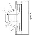
- FIG. 4is a side view showing a stressed liner according to an embodiment of the invention, with the stressed liner in use with a spacer, a gate and a channel.
- FIGS. 5A-5Cdepict an endpoint detection method according to an embodiment of the invention.
- the deposition ratea chemical and/or physical property (such as, e.g., tunable stress) of the formed film.
- This manipulationis accomplished by introducing an additional non-silicon precursor that is otherwise not a traditional reagent for producing a nitride film, an oxide film, an oxynitride film, or a carbide film, with examples of the additional non-silicon precursor being a germanium precursor and a carbon precursor.
- the present inventionaccomplishes such advantages by including a non-silicon precursor dopant (such as, e.g., a Ge precursor, etc.) during the deposition process, such as deposition of a silicon nitride film, deposition of a silicon oxide film, deposition of a silicon oxynitride film, deposition of a silicon carbide film, etc.
- a non-silicon precursor dopantsuch as, e.g., a Ge precursor, etc.
- the present inventionmakes possible low-temperature deposition of a nitride film, an oxide film, an oxynitride film and/or a carbide film, by adding germanium to deposition of nitride films and oxide films and oxynitride films and carbide films, especially doped nitride or oxide films.
- germaniumsilicon germanium (SiGe) epitaxy can be done at a lower temperature than silicon epitaxy, and further have discovered that the addition of a germanium (Ge) precursor to a silicon precursor lowers the temperature of the deposition of the film.
- a germanium precursor used in the present inventionmay be, e.g., a known germanium precursor such as the germanium precursors mentioned, e.g., in U.S. Pat. No. 6,429,098 issued Aug. 6, 2002 and U.S. Pat. No. 6,117,750 issued Sep. 12, 2000 to Bensahel et al. (France Telecom) or in U.S. Pat. No. 6,258,664 issued Jul. 10, 2001 to Reinberg (Micron Technology, Inc.). Germanium precursors are commercially available.
- the present inventionprovides for use of at least one germanium precursor in deposition of a silicon nitride, a silicon oxide, a silicon oxynitride, a silicon carbide, etc., which deposition advantageously may, if desired, by a low-temperature deposition, such as, e.g., a deposition at 700° C. or lower, such as, e.g., room temperature and other temperatures.
- a low-temperature depositionsuch as, e.g., a deposition at 700° C. or lower, such as, e.g., room temperature and other temperatures.
- an inventive methodmay proceed at room temperature in a P3i plasma immersion tool, to deposit nitride.
- the production processotherwise may proceed conventionally with regard to ingredients, for example, use of a nitrogen precursor (such as, e.g., NH 3 , etc.) and a silicon precursor (such as DCS, etc.), etc.
- a nitrogen precursorsuch as, e.g., NH 3 , etc.
- a silicon precursorsuch as DCS, etc.
- a nitrogen precursoris included.
- an oxygen precursoris included.
- a silicon precursoris included. It will be appreciated that the silicon precursor may be different or the same as the nitride or oxide precursor.
- BTBASmay serve as a silicon precursor and a nitrogen precursor.
- a reagentsuch as, e.g., BTBAS, etc.
- BTBASmay be used as two or more kinds of precursors.
- An exemplary temperature for nitride or oxide or oxynitride or carbide film forming using a germanium precursor and/or a carbon precursor according to the inventionis preferably at a temperature less than 700° C., more preferably at a temperature less than 650° C., even more preferably at a temperature of 500° C. or lower.
- an advantageous temperature of 500° C. or lowermay be used for the deposition of a Ge-doped silicon nitride film.
- the non-silicon precursor mentioned for use in the present inventionis not particularly limited, and as examples may be mentioned a germanium precursor, a carbon precursor, an aluminum precursor, a boron precursor, an arsenic precursor, a hafnium precursor, a gallium precursor, an indium precursor, and, without limitation, other dopant precursors, etc.
- the present inventionalso may be applied to MOL barrier technology.
- MOL barrier nitridecan enhance device reliability (negative bias temperature instability (NBTI), etc.).
- NBTInegative bias temperature instability
- the present inventionprovides, through use of the germanium precursor and/or the carbon precursor, an ability to tune the chemical and/or physical properties of the barrier nitride film using different precursor combinations. Such an ability may be used to achieve a significant device reliability gain.
- Thickness of a film produced according to the present inventionis not particularly limited, and a thickness may be selected depending on the application.
- the film thicknessmay range from, on the thin end (such as, e.g., a film of 500 Angstroms, or of 10 Angstroms, or thinner), to the thick end (such as, e.g., a film of 1,000 Angstroms, or a film of 5,000 Angstroms, or thicker), and thicknesses in between, such as films in a range of about 10 to 5,000 Angstroms, and thinner or thicker as called for by the application.
- the dopant concentration of a film made according to the inventionis not particularly, and may be adjusted as desired.
- An example of a dopant (such as Ge, etc.) concentrationis in a range of, e.g., about 1 to 10%, or, in another example, about 1 to 50%.
- the present inventionincludes an embodiment in which multiple non-silicon precursors are used, such as a germanium precursor and a carbon precursor; a germanium precursor and a boron precursor; etc.
- multiple non-silicon precursorssuch as a germanium precursor and a carbon precursor; a germanium precursor and a boron precursor; etc.
- adding multiple precursors during deposition of a silicon nitride or a silicon oxide filmmay provide an enhanced effect, as may be desired.
- the present inventionmay be used, e.g., for signaling an etch end point.
- an etch end pointFor example, when conventional silicon nitride etching is performed, there has been a problem with wanting to stop the etch at the end of the silicon nitride and not etch over onto the silicon. However, such an etch end point many times has not been sharp and etching into the silicon has been common with the conventional methods.
- a doped silicon nitridesuch as a Ge-doped silicon nitride
- the presence of the Ge in the silicon nitridemay be used to signal the endpoint of the etch, thereby advantageously preventing over-etching, such as, e.g., by using optical emission spectroscopy to detect the Ge (e.g., a Ge-Fluoride signal may be searched-for).
- Such an aforementioned etch-stop exampleis not limiting, and the invention is extended to a variety of signaling uses of a dopant in a doped nitride film or a doped oxide film.
- a dopant in a doped nitride film or a doped oxide filmthere may be provided a thin silicon nitride layer doped as an etch stop layer (such as a Ge-doped silicon nitride layer, etc.), and the dopant signal (e.g., the Ge signal, etc.) may be monitored for determining where the layer begins.
- a number of different implementations of the present inventionmay be provided, in the etching context.
- Another exampleis a thin layer of carbon or boron doped oxide under a Ge-doped nitride.
- a further example of using the invention in an etching processis use of two different dopants, such as providing one dopant in each of the respective layers, or providing the two different dopants in a same layer. It will be appreciated that the present invention includes use of different signals being controlled for maximal sensitivity, and that the above-mentioned are only some examples.
- Another use of the present inventionis to change stress of a produced film (e.g., a silicon nitride, silicon oxide) by including a dopant, compared to a film in which the dopant is not included.
- a produced filme.g., a silicon nitride, silicon oxide
- dopante.g., silicon nitride, silicon oxide
- inclusion of a Ge dopanthas been found to change stress of the film to the tensile region.
- RTCVD silicon nitride filmshave a stress of about 1 to 1.5 GPa (tensile).
- Including Ge in the silicon nitride filmsprovides a significant change raising the stress of the film, such as a doped Ge-silicon nitride film with a stress exceeding 1.5 GPa (tensile), such as a stress of 2 GPa (tensile), or higher, etc.
- a delta of 1 GPa or greaterpreferably, such as a delta of 1.2 GPa or greater
- the present inventionmay be used to change the stress of a film from compressive to tensile, which signifies a significant change in the nature of a film.
- the present inventionadvantageously may be used to tune stress of a silicon nitride or silicon oxide film or silicon oxynitride or silicon carbide film as desired.
- the present inventionmay be used to produce doped silicon nitride films, doped silicon oxide films, doped silicon oxynitride films, and doped silicon carbide films, such as, e.g., a Ge-doped silicon nitride film, an Al-doped silicon oxide film, a boron-doped silicon nitride film, etc.
- the bottom plot in FIG. 1is for the film deposited at 650° C., with the same ratios as for the film deposited at 700° C.
- germaneto a mixture of a silicon precursor and ammonia allows for: increasing the deposition rate of an existing process making the process more manufacturable; lowering the deposition rate of a process to make it extendable to future technology; and/or manipulating stress of the formed film.
- the present inventorshave recognized that stress in a film may be modified by germanium addition during nitride film formation. There may be considered the following results, both for silicon substrates: (i) for a Si—N film, stress of 4 E9 Dyne/cm 2 (compressive); (ii) for a SiGe—N film, stress of 8.2 E9 Dyne/cm 2 (tensile).
- deposition rate and/or stress tuningare not limited to nitride films, and may be applicable for oxide films (such as silicon oxide films, etc.) and other films, such as other amorphous films.
- Gewas added to a mixture of silane and ammonia, forming a Ge-doped Si nitride film.
- the deposition ratewas increased for the germane process, compared to an equivalent no-germane process.
- the stress of the produced filmwas 0.4 GPa (compressive).
- the stresswas 0.8 GPa (tensile).
- the use of Ge according to the inventionachieved a change in stress of 1.2 GPa, which was a substantial improvement.
- Stressed nitride liner 40(produced according to the invention) is shown in use with spacer 41 , gate (POLY) with layer 44 (silicide), with the gate being over a channel (SOI).
- POLYgate
- SOIchannel
- FIGS. 5A-5Can example of a counter-doped nitride or oxide layer for endpoint detection according to the invention is shown.
- a spacer nitride 51(with a first dopant) is provided over a nitride or oxide layer 50 (with a second dopant).
- the as-deposited films of FIG. 5Aare processed according to an initial RIE step shown in FIG. 5B , wherein during initial RIE, the first dopant is detected.
- a step of final RIEis performed, as shown in FIG. 5C , wherein an etch endpoint is reached.
- a smaller amount of the first dopant (in the spacer nitride 51 or etched spacer nitride 51 ′)is detected, and detection of the second dopant (in the nitride or oxide layer 50 ) begins.
- a controllably etched spacer nitride 51 ′remains.
Landscapes
- Chemical & Material Sciences (AREA)
- Engineering & Computer Science (AREA)
- Condensed Matter Physics & Semiconductors (AREA)
- General Physics & Mathematics (AREA)
- General Chemical & Material Sciences (AREA)
- Materials Engineering (AREA)
- Mechanical Engineering (AREA)
- Metallurgy (AREA)
- Organic Chemistry (AREA)
- Physics & Mathematics (AREA)
- Inorganic Chemistry (AREA)
- Chemical Kinetics & Catalysis (AREA)
- Manufacturing & Machinery (AREA)
- Computer Hardware Design (AREA)
- Microelectronics & Electronic Packaging (AREA)
- Power Engineering (AREA)
- Formation Of Insulating Films (AREA)
- Chemical Vapour Deposition (AREA)
- Internal Circuitry In Semiconductor Integrated Circuit Devices (AREA)
- Insulated Gate Type Field-Effect Transistor (AREA)
- Electrodes Of Semiconductors (AREA)
- Thin Film Transistor (AREA)
Abstract
Description
Claims (1)
Priority Applications (1)
| Application Number | Priority Date | Filing Date | Title |
|---|---|---|---|
| US11/924,825US7595010B2 (en) | 2004-06-29 | 2007-10-26 | Method for producing a doped nitride film, doped oxide film and other doped films |
Applications Claiming Priority (3)
| Application Number | Priority Date | Filing Date | Title |
|---|---|---|---|
| US10/710,245US20050287747A1 (en) | 2004-06-29 | 2004-06-29 | Doped nitride film, doped oxide film and other doped films |
| US11/349,233US7361611B2 (en) | 2004-06-29 | 2006-02-08 | Doped nitride film, doped oxide film and other doped films |
| US11/924,825US7595010B2 (en) | 2004-06-29 | 2007-10-26 | Method for producing a doped nitride film, doped oxide film and other doped films |
Related Parent Applications (1)
| Application Number | Title | Priority Date | Filing Date |
|---|---|---|---|
| US11/349,233ContinuationUS7361611B2 (en) | 2004-06-29 | 2006-02-08 | Doped nitride film, doped oxide film and other doped films |
Publications (2)
| Publication Number | Publication Date |
|---|---|
| US20080054228A1 US20080054228A1 (en) | 2008-03-06 |
| US7595010B2true US7595010B2 (en) | 2009-09-29 |
Family
ID=35506413
Family Applications (4)
| Application Number | Title | Priority Date | Filing Date |
|---|---|---|---|
| US10/710,245AbandonedUS20050287747A1 (en) | 2004-06-29 | 2004-06-29 | Doped nitride film, doped oxide film and other doped films |
| US11/349,233Expired - LifetimeUS7361611B2 (en) | 2004-06-29 | 2006-02-08 | Doped nitride film, doped oxide film and other doped films |
| US11/428,648AbandonedUS20060237846A1 (en) | 2004-06-29 | 2006-07-05 | Doped nitride film, doped oxide film and other doped films and deposition rate improvement for rtcvd processes |
| US11/924,825Expired - Fee RelatedUS7595010B2 (en) | 2004-06-29 | 2007-10-26 | Method for producing a doped nitride film, doped oxide film and other doped films |
Family Applications Before (3)
| Application Number | Title | Priority Date | Filing Date |
|---|---|---|---|
| US10/710,245AbandonedUS20050287747A1 (en) | 2004-06-29 | 2004-06-29 | Doped nitride film, doped oxide film and other doped films |
| US11/349,233Expired - LifetimeUS7361611B2 (en) | 2004-06-29 | 2006-02-08 | Doped nitride film, doped oxide film and other doped films |
| US11/428,648AbandonedUS20060237846A1 (en) | 2004-06-29 | 2006-07-05 | Doped nitride film, doped oxide film and other doped films and deposition rate improvement for rtcvd processes |
Country Status (4)
| Country | Link |
|---|---|
| US (4) | US20050287747A1 (en) |
| JP (1) | JP5078240B2 (en) |
| CN (1) | CN100428424C (en) |
| TW (1) | TWI355684B (en) |
Cited By (30)
| Publication number | Priority date | Publication date | Assignee | Title |
|---|---|---|---|---|
| US20080124946A1 (en)* | 2006-11-28 | 2008-05-29 | Air Products And Chemicals, Inc. | Organosilane compounds for modifying dielectrical properties of silicon oxide and silicon nitride films |
| US20120081197A1 (en)* | 2010-10-01 | 2012-04-05 | Electronics And Telecommunications Research Institute | Method of tuning resonance wavelength of ring resonator |
| US8999859B2 (en) | 2010-04-15 | 2015-04-07 | Novellus Systems, Inc. | Plasma activated conformal dielectric film deposition |
| US9214334B2 (en) | 2014-02-18 | 2015-12-15 | Lam Research Corporation | High growth rate process for conformal aluminum nitride |
| US9230800B2 (en) | 2010-04-15 | 2016-01-05 | Novellus Systems, Inc. | Plasma activated conformal film deposition |
| US9257274B2 (en) | 2010-04-15 | 2016-02-09 | Lam Research Corporation | Gapfill of variable aspect ratio features with a composite PEALD and PECVD method |
| US9287113B2 (en) | 2012-11-08 | 2016-03-15 | Novellus Systems, Inc. | Methods for depositing films on sensitive substrates |
| US9355839B2 (en) | 2012-10-23 | 2016-05-31 | Lam Research Corporation | Sub-saturated atomic layer deposition and conformal film deposition |
| US9355886B2 (en) | 2010-04-15 | 2016-05-31 | Novellus Systems, Inc. | Conformal film deposition for gapfill |
| US9373500B2 (en) | 2014-02-21 | 2016-06-21 | Lam Research Corporation | Plasma assisted atomic layer deposition titanium oxide for conformal encapsulation and gapfill applications |
| US9390909B2 (en) | 2013-11-07 | 2016-07-12 | Novellus Systems, Inc. | Soft landing nanolaminates for advanced patterning |
| US9478438B2 (en) | 2014-08-20 | 2016-10-25 | Lam Research Corporation | Method and apparatus to deposit pure titanium thin film at low temperature using titanium tetraiodide precursor |
| US9478411B2 (en) | 2014-08-20 | 2016-10-25 | Lam Research Corporation | Method to tune TiOx stoichiometry using atomic layer deposited Ti film to minimize contact resistance for TiOx/Ti based MIS contact scheme for CMOS |
| US9502238B2 (en) | 2015-04-03 | 2016-11-22 | Lam Research Corporation | Deposition of conformal films by atomic layer deposition and atomic layer etch |
| US9564312B2 (en) | 2014-11-24 | 2017-02-07 | Lam Research Corporation | Selective inhibition in atomic layer deposition of silicon-containing films |
| US9611544B2 (en) | 2010-04-15 | 2017-04-04 | Novellus Systems, Inc. | Plasma activated conformal dielectric film deposition |
| US9685320B2 (en) | 2010-09-23 | 2017-06-20 | Lam Research Corporation | Methods for depositing silicon oxide |
| US9773643B1 (en) | 2016-06-30 | 2017-09-26 | Lam Research Corporation | Apparatus and method for deposition and etch in gap fill |
| US9799509B2 (en) | 2014-11-26 | 2017-10-24 | Asm Ip Holding B.V. | Cyclic aluminum oxynitride deposition |
| US9837281B2 (en) | 2014-11-26 | 2017-12-05 | Asm Ip Holding B.V. | Cyclic doped aluminum nitride deposition |
| US9892917B2 (en) | 2010-04-15 | 2018-02-13 | Lam Research Corporation | Plasma assisted atomic layer deposition of multi-layer films for patterning applications |
| US9997357B2 (en) | 2010-04-15 | 2018-06-12 | Lam Research Corporation | Capped ALD films for doping fin-shaped channel regions of 3-D IC transistors |
| US10037884B2 (en) | 2016-08-31 | 2018-07-31 | Lam Research Corporation | Selective atomic layer deposition for gapfill using sacrificial underlayer |
| US10062563B2 (en) | 2016-07-01 | 2018-08-28 | Lam Research Corporation | Selective atomic layer deposition with post-dose treatment |
| US10269559B2 (en) | 2017-09-13 | 2019-04-23 | Lam Research Corporation | Dielectric gapfill of high aspect ratio features utilizing a sacrificial etch cap layer |
| US10510530B2 (en) | 2011-11-04 | 2019-12-17 | Asm International N.V. | Methods for forming doped silicon oxide thin films |
| US10526701B2 (en) | 2015-07-09 | 2020-01-07 | Lam Research Corporation | Multi-cycle ALD process for film uniformity and thickness profile modulation |
| US11646198B2 (en) | 2015-03-20 | 2023-05-09 | Lam Research Corporation | Ultrathin atomic layer deposition film accuracy thickness control |
| US12040181B2 (en) | 2019-05-01 | 2024-07-16 | Lam Research Corporation | Modulated atomic layer deposition |
| US12431349B2 (en) | 2019-06-07 | 2025-09-30 | Lam Research Corporation | In-situ control of film properties during atomic layer deposition |
Families Citing this family (71)
| Publication number | Priority date | Publication date | Assignee | Title |
|---|---|---|---|---|
| US7119016B2 (en)* | 2003-10-15 | 2006-10-10 | International Business Machines Corporation | Deposition of carbon and nitrogen doped poly silicon films, and retarded boron diffusion and improved poly depletion |
| US20050287747A1 (en)* | 2004-06-29 | 2005-12-29 | International Business Machines Corporation | Doped nitride film, doped oxide film and other doped films |
| US7288205B2 (en)* | 2004-07-09 | 2007-10-30 | Applied Materials, Inc. | Hermetic low dielectric constant layer for barrier applications |
| JP2006165335A (en)* | 2004-12-08 | 2006-06-22 | Toshiba Corp | Semiconductor device |
| US20060172556A1 (en)* | 2005-02-01 | 2006-08-03 | Texas Instruments Incorporated | Semiconductor device having a high carbon content strain inducing film and a method of manufacture therefor |
| US7462527B2 (en)* | 2005-07-06 | 2008-12-09 | International Business Machines Corporation | Method of forming nitride films with high compressive stress for improved PFET device performance |
| US20070087581A1 (en)* | 2005-09-09 | 2007-04-19 | Varian Semiconductor Equipment Associates, Inc. | Technique for atomic layer deposition |
| US20070065576A1 (en)* | 2005-09-09 | 2007-03-22 | Vikram Singh | Technique for atomic layer deposition |
| US7371649B2 (en)* | 2005-09-13 | 2008-05-13 | United Microelectronics Corp. | Method of forming carbon-containing silicon nitride layer |
| US20070082507A1 (en)* | 2005-10-06 | 2007-04-12 | Applied Materials, Inc. | Method and apparatus for the low temperature deposition of doped silicon nitride films |
| US7416995B2 (en)* | 2005-11-12 | 2008-08-26 | Applied Materials, Inc. | Method for fabricating controlled stress silicon nitride films |
| CN101473382A (en)* | 2006-05-12 | 2009-07-01 | 高级技术材料公司 | Low temperature deposition of phase change memory materials |
| US7514370B2 (en)* | 2006-05-19 | 2009-04-07 | International Business Machines Corporation | Compressive nitride film and method of manufacturing thereof |
| US7501355B2 (en) | 2006-06-29 | 2009-03-10 | Applied Materials, Inc. | Decreasing the etch rate of silicon nitride by carbon addition |
| KR100772836B1 (en) | 2006-07-21 | 2007-11-01 | 동부일렉트로닉스 주식회사 | Manufacturing Method of Semiconductor Device |
| KR100761857B1 (en)* | 2006-09-08 | 2007-09-28 | 삼성전자주식회사 | Method of forming fine pattern of semiconductor device and manufacturing method of semiconductor device using same |
| CN102352488B (en) | 2006-11-02 | 2016-04-06 | 诚实公司 | The antimony useful for the CVD/ALD of metallic film and germanium complexes |
| US7790635B2 (en)* | 2006-12-14 | 2010-09-07 | Applied Materials, Inc. | Method to increase the compressive stress of PECVD dielectric films |
| US20080145978A1 (en)* | 2006-12-18 | 2008-06-19 | Air Liquide Electronics U.S. Lp | Deposition of silicon germanium nitrogen precursors for strain engineering |
| US20080293194A1 (en)* | 2007-05-24 | 2008-11-27 | Neng-Kuo Chen | Method of making a P-type metal-oxide semiconductor transistor and method of making a complementary metal-oxide semiconductor transistor |
| US8084356B2 (en)* | 2007-09-29 | 2011-12-27 | Lam Research Corporation | Methods of low-K dielectric and metal process integration |
| US8834968B2 (en) | 2007-10-11 | 2014-09-16 | Samsung Electronics Co., Ltd. | Method of forming phase change material layer using Ge(II) source, and method of fabricating phase change memory device |
| KR101458953B1 (en) | 2007-10-11 | 2014-11-07 | 삼성전자주식회사 | Method of forming phase change material layer using Ge(Ⅱ) source, and method of fabricating phase change memory device |
| US8987039B2 (en)* | 2007-10-12 | 2015-03-24 | Air Products And Chemicals, Inc. | Antireflective coatings for photovoltaic applications |
| US20090096106A1 (en)* | 2007-10-12 | 2009-04-16 | Air Products And Chemicals, Inc. | Antireflective coatings |
| US7994066B1 (en)* | 2007-10-13 | 2011-08-09 | Luxtera, Inc. | Si surface cleaning for semiconductor circuits |
| US7994042B2 (en)* | 2007-10-26 | 2011-08-09 | International Business Machines Corporation | Techniques for impeding reverse engineering |
| SG178736A1 (en)* | 2007-10-31 | 2012-03-29 | Advanced Tech Materials | Amorphous ge/te deposition process |
| JP2009164260A (en) | 2007-12-28 | 2009-07-23 | Toshiba Corp | Nonvolatile semiconductor memory |
| JP2009200095A (en)* | 2008-02-19 | 2009-09-03 | Tokyo Electron Ltd | Thin film and method for manufacturing semiconductor device using this thin film |
| US20090215225A1 (en) | 2008-02-24 | 2009-08-27 | Advanced Technology Materials, Inc. | Tellurium compounds useful for deposition of tellurium containing materials |
| JP2009260151A (en)* | 2008-04-18 | 2009-11-05 | Tokyo Electron Ltd | Method of forming metal doped layer, film forming apparatus, and storage medium |
| US8343824B2 (en)* | 2008-04-29 | 2013-01-01 | International Rectifier Corporation | Gallium nitride material processing and related device structures |
| US20110180905A1 (en)* | 2008-06-10 | 2011-07-28 | Advanced Technology Materials, Inc. | GeSbTe MATERIAL INCLUDING SUPERFLOW LAYER(S), AND USE OF Ge TO PREVENT INTERACTION OF Te FROM SbXTeY AND GeXTeY RESULTING IN HIGH Te CONTENT AND FILM CRYSTALLINITY |
| WO2010065874A2 (en) | 2008-12-05 | 2010-06-10 | Atmi | High concentration nitrogen-containing germanium telluride based memory devices and processes of making |
| KR20160084491A (en) | 2009-05-22 | 2016-07-13 | 엔테그리스, 아이엔씨. | Low temperature gst process |
| US8791034B2 (en)* | 2009-06-26 | 2014-07-29 | Cornell University | Chemical vapor deposition process for aluminum silicon nitride |
| KR101602007B1 (en)* | 2009-07-02 | 2016-03-09 | 인티그리스, 인코포레이티드 | Hollow gst structure with dielectric fill |
| US20110124182A1 (en)* | 2009-11-20 | 2011-05-26 | Advanced Techology Materials, Inc. | System for the delivery of germanium-based precursor |
| CN102194751A (en)* | 2010-03-11 | 2011-09-21 | 中芯国际集成电路制造(上海)有限公司 | Method for manufacturing complementary metal-oxide-semiconductor (CMOS) device |
| TW201132787A (en) | 2010-03-26 | 2011-10-01 | Advanced Tech Materials | Germanium antimony telluride materials and devices incorporating same |
| WO2011125395A1 (en)* | 2010-04-09 | 2011-10-13 | 株式会社日立国際電気 | Process for production of semiconductor device, method for treatment of substrate, and device for treatment of substrate |
| US8993460B2 (en)* | 2013-01-10 | 2015-03-31 | Novellus Systems, Inc. | Apparatuses and methods for depositing SiC/SiCN films via cross-metathesis reactions with organometallic co-reactants |
| WO2011146913A2 (en) | 2010-05-21 | 2011-11-24 | Advanced Technology Materials, Inc. | Germanium antimony telluride materials and devices incorporating same |
| US8614478B2 (en) | 2010-07-26 | 2013-12-24 | Infineon Technologies Austria Ag | Method for protecting a semiconductor device against degradation, a semiconductor device protected against hot charge carriers and a manufacturing method therefor |
| US8786012B2 (en) | 2010-07-26 | 2014-07-22 | Infineon Technologies Austria Ag | Power semiconductor device and a method for forming a semiconductor device |
| CN102386089B (en)* | 2010-09-03 | 2013-06-12 | 中芯国际集成电路制造(上海)有限公司 | Method for preparing semiconductor device structure |
| JP5689398B2 (en)* | 2010-12-21 | 2015-03-25 | 東京エレクトロン株式会社 | Method and apparatus for forming silicon nitride film |
| JP5847566B2 (en) | 2011-01-14 | 2016-01-27 | 株式会社日立国際電気 | Semiconductor device manufacturing method, substrate processing method, substrate processing apparatus, and program |
| EP3929326A3 (en) | 2011-06-03 | 2022-03-16 | Versum Materials US, LLC | Compositions and processes for depositing carbon-doped silicon-containing films |
| JP5959307B2 (en) | 2011-06-22 | 2016-08-02 | 株式会社日立国際電気 | Semiconductor device manufacturing method, substrate processing method, substrate processing apparatus, and program |
| JP5793398B2 (en)* | 2011-10-28 | 2015-10-14 | 東京エレクトロン株式会社 | Method for forming seed layer and method for forming silicon-containing thin film |
| US9049061B2 (en)* | 2012-03-21 | 2015-06-02 | The Institute of Microelectronics Chinese Academy of Science | CMOS device and method for manufacturing the same |
| JP5758829B2 (en) | 2012-03-27 | 2015-08-05 | 東京エレクトロン株式会社 | Method for forming boron-containing silicon oxycarbonitride film and method for forming silicon oxycarbonitride film |
| CN102623334B (en)* | 2012-04-17 | 2014-10-22 | 上海华力微电子有限公司 | Method for forming silicon nitride film with double stress layers |
| CN102623409B (en)* | 2012-04-17 | 2014-08-13 | 上海华力微电子有限公司 | Method for forming silicon nitride film with double stress layers |
| CN102623333B (en)* | 2012-04-17 | 2014-09-03 | 上海华力微电子有限公司 | Method for forming silicon nitride film with double stress layers |
| US9640757B2 (en) | 2012-10-30 | 2017-05-02 | Entegris, Inc. | Double self-aligned phase change memory device structure |
| US9500773B2 (en)* | 2013-06-07 | 2016-11-22 | Lawrence Livermore National Security, Llc | High voltage photoconductive switch package |
| JP6378070B2 (en)* | 2014-12-15 | 2018-08-22 | 東京エレクトロン株式会社 | Deposition method |
| TWI663281B (en)* | 2015-06-16 | 2019-06-21 | 美商慧盛材料美國責任有限公司 | Preparation and composition of halidosilane compounds, and container containing same |
| CN105047559B (en)* | 2015-08-12 | 2018-01-12 | 沈阳拓荆科技有限公司 | The method for highly obtaining different performance silicon nitride film by adjusting jewel ball |
| CN105256375B (en)* | 2015-09-02 | 2017-10-31 | 光昱(厦门)新能源有限公司 | A kind of method for improving solar cell diffusion furnace silicon carbide paddle fatigue resistance |
| TWI642803B (en)* | 2015-09-11 | 2018-12-01 | 慧盛材料美國責任有限公司 | Methods for depositing a conformal metal or metalloid silicon nitride film and resultant films |
| KR102153564B1 (en)* | 2015-10-06 | 2020-09-08 | 버슘머트리얼즈 유에스, 엘엘씨 | Method of depositing conformal metal or metalloid silicon nitride film |
| CN106449907B (en)* | 2016-11-18 | 2019-04-12 | 电子科技大学 | A kind of growing method of p-type exponential doping structure GaN photoelectric cathode materials |
| US10529563B2 (en)* | 2017-03-29 | 2020-01-07 | Asm Ip Holdings B.V. | Method for forming doped metal oxide films on a substrate by cyclical deposition and related semiconductor device structures |
| CN108417481B (en)* | 2018-03-22 | 2021-02-23 | 京东方科技集团股份有限公司 | Method for processing silicon nitride dielectric layer, thin film transistor and display device |
| US11276573B2 (en)* | 2019-12-04 | 2022-03-15 | Applied Materials, Inc. | Methods of forming high boron-content hard mask materials |
| US11674222B2 (en) | 2020-09-29 | 2023-06-13 | Applied Materials, Inc. | Method of in situ ceramic coating deposition |
| US20220195606A1 (en)* | 2020-12-23 | 2022-06-23 | Raytheon Technologies Corporation | Method for metal vapor infiltration of cmc parts and articles containing the same |
Citations (25)
| Publication number | Priority date | Publication date | Assignee | Title |
|---|---|---|---|---|
| US4091169A (en) | 1975-12-18 | 1978-05-23 | International Business Machines Corporation | Silicon oxide/silicon nitride mask with improved integrity for semiconductor fabrication |
| US4126880A (en) | 1976-02-13 | 1978-11-21 | Hitachi, Ltd. | Germanium-containing silicon nitride film |
| JPS56169333A (en) | 1980-05-29 | 1981-12-26 | Fujitsu Ltd | Semiconductor device |
| US4743563A (en) | 1987-05-26 | 1988-05-10 | Motorola, Inc. | Process of controlling surface doping |
| US5347100A (en)* | 1991-03-29 | 1994-09-13 | Hitachi, Ltd. | Semiconductor device, process for the production thereof and apparatus for microwave plasma treatment |
| EP0724286A1 (en)* | 1995-01-25 | 1996-07-31 | Applied Materials, Inc. | A method of forming a thin film of silicon oxide for a semiconductor device |
| EP0822585A2 (en)* | 1996-08-02 | 1998-02-04 | Applied Materials, Inc. | Stress control by fluorination of silica film |
| US5750211A (en)* | 1991-05-17 | 1998-05-12 | Lam Research Corporation | Process for depositing a SiOx film having reduced intrinsic stress and/or reduced hydrogen content |
| US6117750A (en) | 1997-12-29 | 2000-09-12 | France Telecom | Process for obtaining a layer of single-crystal germanium or silicon on a substrate of single-crystal silicon or germanium, respectively |
| US6121164A (en) | 1997-10-24 | 2000-09-19 | Applied Materials, Inc. | Method for forming low compressive stress fluorinated ozone/TEOS oxide film |
| US6146972A (en) | 1997-06-11 | 2000-11-14 | Nec Corporation | Method for fabricating semiconductor device |
| US6162737A (en)* | 1998-11-24 | 2000-12-19 | Micron Technology, Inc. | Films doped with carbon for use in integrated circuit technology |
| US6258664B1 (en) | 1999-02-16 | 2001-07-10 | Micron Technology, Inc. | Methods of forming silicon-comprising materials having roughened outer surfaces, and methods of forming capacitor constructions |
| US6261975B1 (en) | 1999-03-04 | 2001-07-17 | Applied Materials, Inc. | Method for depositing and planarizing fluorinated BPSG films |
| US6280651B1 (en) | 1998-12-16 | 2001-08-28 | Advanced Technology Materials, Inc. | Selective silicon oxide etchant formulation including fluoride salt, chelating agent, and glycol solvent |
| US6306722B1 (en)* | 1999-05-03 | 2001-10-23 | United Microelectronics Corp. | Method for fabricating shallow trench isolation structure |
| US20020194876A1 (en)* | 2001-05-11 | 2002-12-26 | International Business Machines Corporation | Method for manufacturing an optical device with a defined total device stress |
| US6624093B1 (en)* | 2002-10-09 | 2003-09-23 | Wisys Technology Foundation | Method of producing high dielectric insulator for integrated circuit |
| US20040013009A1 (en) | 2002-04-04 | 2004-01-22 | Kabushiki Kaisha Toshiba | Semiconductor memory device having a gate electrode and a method of manufacturing thereof |
| US20040029323A1 (en) | 2000-11-22 | 2004-02-12 | Akihiro Shimizu | Semiconductor device and method for fabricating the same |
| US20040198069A1 (en)* | 2003-04-04 | 2004-10-07 | Applied Materials, Inc. | Method for hafnium nitride deposition |
| US20040240820A1 (en)* | 2001-07-12 | 2004-12-02 | Johnson Frederick G. | Silicon-oxycarbide high index contrast, low-loss optical waveguides and integrated thermo-optic devices |
| US20050093076A1 (en) | 2003-11-05 | 2005-05-05 | International Business Machines Corporation | METHOD AND STRUCTURE FOR FORMING STRAINED Si FOR CMOS DEVICES |
| US20050093078A1 (en) | 2003-10-30 | 2005-05-05 | Victor Chan | Increasing carrier mobility in NFET and PFET transistors on a common wafer |
| US20050287747A1 (en)* | 2004-06-29 | 2005-12-29 | International Business Machines Corporation | Doped nitride film, doped oxide film and other doped films |
Family Cites Families (22)
| Publication number | Priority date | Publication date | Assignee | Title |
|---|---|---|---|---|
| JPS5298473A (en)* | 1976-02-13 | 1977-08-18 | Hitachi Ltd | Thin film material |
| JPS5693375A (en)* | 1979-12-26 | 1981-07-28 | Shunpei Yamazaki | Photoelectric conversion device |
| JPS56122123A (en)* | 1980-03-03 | 1981-09-25 | Shunpei Yamazaki | Semiamorphous semiconductor |
| US4892753A (en)* | 1986-12-19 | 1990-01-09 | Applied Materials, Inc. | Process for PECVD of silicon oxide using TEOS decomposition |
| JPH01176067A (en)* | 1987-12-29 | 1989-07-12 | Hoya Corp | Formation of silicon nitride film |
| JP2663508B2 (en)* | 1988-05-12 | 1997-10-15 | ソニー株式会社 | Vapor growth method |
| JPH02233531A (en)* | 1989-03-07 | 1990-09-17 | Sony Corp | Coating glass composition and semiconductor device |
| JPH0770531B2 (en)* | 1989-06-30 | 1995-07-31 | 川崎製鉄株式会社 | Method for forming buried oxide film |
| JPH04165623A (en)* | 1990-10-30 | 1992-06-11 | Nec Corp | Method of forming silicon boron nitride film |
| US5478765A (en)* | 1994-05-04 | 1995-12-26 | Regents Of The University Of Texas System | Method of making an ultra thin dielectric for electronic devices |
| JP3597305B2 (en)* | 1996-03-05 | 2004-12-08 | 株式会社半導体エネルギー研究所 | Liquid crystal display device and manufacturing method thereof |
| US5741737A (en)* | 1996-06-27 | 1998-04-21 | Cypress Semiconductor Corporation | MOS transistor with ramped gate oxide thickness and method for making same |
| US5997634A (en)* | 1996-11-14 | 1999-12-07 | Micron Technology, Inc. | Method of forming a crystalline phase material |
| US5972765A (en)* | 1997-07-16 | 1999-10-26 | International Business Machines Corporation | Use of deuterated materials in semiconductor processing |
| US5976991A (en)* | 1998-06-11 | 1999-11-02 | Air Products And Chemicals, Inc. | Deposition of silicon dioxide and silicon oxynitride using bis(tertiarybutylamino) silane |
| US7002071B1 (en)* | 1999-03-10 | 2006-02-21 | Sumitomo Special Metals Co. Ltd. | Thermoelectric conversion material and method of producing the same |
| DE60213555T2 (en)* | 2002-03-28 | 2007-08-09 | Fluid Automation Systems S.A. | Electromagnetic valve |
| KR100769783B1 (en)* | 2002-03-29 | 2007-10-24 | 가부시끼가이샤 도시바 | Display input device and display input system |
| US6930058B2 (en)* | 2003-04-21 | 2005-08-16 | Micron Technology, Inc. | Method of depositing a silicon dioxide comprising layer doped with at least one of P, B and Ge |
| US7119016B2 (en)* | 2003-10-15 | 2006-10-10 | International Business Machines Corporation | Deposition of carbon and nitrogen doped poly silicon films, and retarded boron diffusion and improved poly depletion |
| US20050109276A1 (en)* | 2003-11-25 | 2005-05-26 | Applied Materials, Inc. | Thermal chemical vapor deposition of silicon nitride using BTBAS bis(tertiary-butylamino silane) in a single wafer chamber |
| US7001844B2 (en)* | 2004-04-30 | 2006-02-21 | International Business Machines Corporation | Material for contact etch layer to enhance device performance |
- 2004
- 2004-06-29USUS10/710,245patent/US20050287747A1/ennot_activeAbandoned
- 2005
- 2005-06-03TWTW094118424Apatent/TWI355684B/ennot_activeIP Right Cessation
- 2005-06-22JPJP2005182180Apatent/JP5078240B2/ennot_activeExpired - Fee Related
- 2005-06-24CNCNB2005100809411Apatent/CN100428424C/ennot_activeExpired - Lifetime
- 2006
- 2006-02-08USUS11/349,233patent/US7361611B2/ennot_activeExpired - Lifetime
- 2006-07-05USUS11/428,648patent/US20060237846A1/ennot_activeAbandoned
- 2007
- 2007-10-26USUS11/924,825patent/US7595010B2/ennot_activeExpired - Fee Related
Patent Citations (26)
| Publication number | Priority date | Publication date | Assignee | Title |
|---|---|---|---|---|
| US4091169A (en) | 1975-12-18 | 1978-05-23 | International Business Machines Corporation | Silicon oxide/silicon nitride mask with improved integrity for semiconductor fabrication |
| US4126880A (en) | 1976-02-13 | 1978-11-21 | Hitachi, Ltd. | Germanium-containing silicon nitride film |
| JPS56169333A (en) | 1980-05-29 | 1981-12-26 | Fujitsu Ltd | Semiconductor device |
| US4743563A (en) | 1987-05-26 | 1988-05-10 | Motorola, Inc. | Process of controlling surface doping |
| US5347100A (en)* | 1991-03-29 | 1994-09-13 | Hitachi, Ltd. | Semiconductor device, process for the production thereof and apparatus for microwave plasma treatment |
| US5750211A (en)* | 1991-05-17 | 1998-05-12 | Lam Research Corporation | Process for depositing a SiOx film having reduced intrinsic stress and/or reduced hydrogen content |
| EP0724286A1 (en)* | 1995-01-25 | 1996-07-31 | Applied Materials, Inc. | A method of forming a thin film of silicon oxide for a semiconductor device |
| EP0822585A2 (en)* | 1996-08-02 | 1998-02-04 | Applied Materials, Inc. | Stress control by fluorination of silica film |
| US6146972A (en) | 1997-06-11 | 2000-11-14 | Nec Corporation | Method for fabricating semiconductor device |
| US6121164A (en) | 1997-10-24 | 2000-09-19 | Applied Materials, Inc. | Method for forming low compressive stress fluorinated ozone/TEOS oxide film |
| US6117750A (en) | 1997-12-29 | 2000-09-12 | France Telecom | Process for obtaining a layer of single-crystal germanium or silicon on a substrate of single-crystal silicon or germanium, respectively |
| US6429098B1 (en) | 1997-12-29 | 2002-08-06 | FRANCE TéLéCOM | Process for obtaining a layer of single-crystal germanium or silicon on a substrate of single-crystal silicon or germanium, respectively, and multilayer products obtained |
| US6162737A (en)* | 1998-11-24 | 2000-12-19 | Micron Technology, Inc. | Films doped with carbon for use in integrated circuit technology |
| US6280651B1 (en) | 1998-12-16 | 2001-08-28 | Advanced Technology Materials, Inc. | Selective silicon oxide etchant formulation including fluoride salt, chelating agent, and glycol solvent |
| US6258664B1 (en) | 1999-02-16 | 2001-07-10 | Micron Technology, Inc. | Methods of forming silicon-comprising materials having roughened outer surfaces, and methods of forming capacitor constructions |
| US6261975B1 (en) | 1999-03-04 | 2001-07-17 | Applied Materials, Inc. | Method for depositing and planarizing fluorinated BPSG films |
| US6306722B1 (en)* | 1999-05-03 | 2001-10-23 | United Microelectronics Corp. | Method for fabricating shallow trench isolation structure |
| US20040029323A1 (en) | 2000-11-22 | 2004-02-12 | Akihiro Shimizu | Semiconductor device and method for fabricating the same |
| US20020194876A1 (en)* | 2001-05-11 | 2002-12-26 | International Business Machines Corporation | Method for manufacturing an optical device with a defined total device stress |
| US20040240820A1 (en)* | 2001-07-12 | 2004-12-02 | Johnson Frederick G. | Silicon-oxycarbide high index contrast, low-loss optical waveguides and integrated thermo-optic devices |
| US20040013009A1 (en) | 2002-04-04 | 2004-01-22 | Kabushiki Kaisha Toshiba | Semiconductor memory device having a gate electrode and a method of manufacturing thereof |
| US6624093B1 (en)* | 2002-10-09 | 2003-09-23 | Wisys Technology Foundation | Method of producing high dielectric insulator for integrated circuit |
| US20040198069A1 (en)* | 2003-04-04 | 2004-10-07 | Applied Materials, Inc. | Method for hafnium nitride deposition |
| US20050093078A1 (en) | 2003-10-30 | 2005-05-05 | Victor Chan | Increasing carrier mobility in NFET and PFET transistors on a common wafer |
| US20050093076A1 (en) | 2003-11-05 | 2005-05-05 | International Business Machines Corporation | METHOD AND STRUCTURE FOR FORMING STRAINED Si FOR CMOS DEVICES |
| US20050287747A1 (en)* | 2004-06-29 | 2005-12-29 | International Business Machines Corporation | Doped nitride film, doped oxide film and other doped films |
Non-Patent Citations (1)
| Title |
|---|
| EerNisse, "Stress in ion-implanted CVD Si3N4 Films", J. Applied Physics, Aug. 1997, vol. 48, No. 8, pp. 3337-3341. |
Cited By (56)
| Publication number | Priority date | Publication date | Assignee | Title |
|---|---|---|---|---|
| US20080124946A1 (en)* | 2006-11-28 | 2008-05-29 | Air Products And Chemicals, Inc. | Organosilane compounds for modifying dielectrical properties of silicon oxide and silicon nitride films |
| US9611544B2 (en) | 2010-04-15 | 2017-04-04 | Novellus Systems, Inc. | Plasma activated conformal dielectric film deposition |
| US11133180B2 (en) | 2010-04-15 | 2021-09-28 | Lam Research Corporation | Gapfill of variable aspect ratio features with a composite PEALD and PECVD method |
| US8999859B2 (en) | 2010-04-15 | 2015-04-07 | Novellus Systems, Inc. | Plasma activated conformal dielectric film deposition |
| US12261038B2 (en) | 2010-04-15 | 2025-03-25 | Lam Research Corporation | Gapfill of variable aspect ratio features with a composite PEALD and PECVD method |
| US9230800B2 (en) | 2010-04-15 | 2016-01-05 | Novellus Systems, Inc. | Plasma activated conformal film deposition |
| US9257274B2 (en) | 2010-04-15 | 2016-02-09 | Lam Research Corporation | Gapfill of variable aspect ratio features with a composite PEALD and PECVD method |
| US9997357B2 (en) | 2010-04-15 | 2018-06-12 | Lam Research Corporation | Capped ALD films for doping fin-shaped channel regions of 3-D IC transistors |
| US10043657B2 (en) | 2010-04-15 | 2018-08-07 | Lam Research Corporation | Plasma assisted atomic layer deposition metal oxide for patterning applications |
| US9355886B2 (en) | 2010-04-15 | 2016-05-31 | Novellus Systems, Inc. | Conformal film deposition for gapfill |
| US9673041B2 (en) | 2010-04-15 | 2017-06-06 | Lam Research Corporation | Plasma assisted atomic layer deposition titanium oxide for patterning applications |
| US11011379B2 (en) | 2010-04-15 | 2021-05-18 | Lam Research Corporation | Capped ALD films for doping fin-shaped channel regions of 3-D IC transistors |
| US9793110B2 (en) | 2010-04-15 | 2017-10-17 | Lam Research Corporation | Gapfill of variable aspect ratio features with a composite PEALD and PECVD method |
| US10559468B2 (en) | 2010-04-15 | 2020-02-11 | Lam Research Corporation | Capped ALD films for doping fin-shaped channel regions of 3-D IC transistors |
| US10043655B2 (en) | 2010-04-15 | 2018-08-07 | Novellus Systems, Inc. | Plasma activated conformal dielectric film deposition |
| US10361076B2 (en) | 2010-04-15 | 2019-07-23 | Lam Research Corporation | Gapfill of variable aspect ratio features with a composite PEALD and PECVD method |
| US9570290B2 (en) | 2010-04-15 | 2017-02-14 | Lam Research Corporation | Plasma assisted atomic layer deposition titanium oxide for conformal encapsulation and gapfill applications |
| US9570274B2 (en) | 2010-04-15 | 2017-02-14 | Novellus Systems, Inc. | Plasma activated conformal dielectric film deposition |
| US9892917B2 (en) | 2010-04-15 | 2018-02-13 | Lam Research Corporation | Plasma assisted atomic layer deposition of multi-layer films for patterning applications |
| US9685320B2 (en) | 2010-09-23 | 2017-06-20 | Lam Research Corporation | Methods for depositing silicon oxide |
| US20120081197A1 (en)* | 2010-10-01 | 2012-04-05 | Electronics And Telecommunications Research Institute | Method of tuning resonance wavelength of ring resonator |
| US8644657B2 (en)* | 2010-10-01 | 2014-02-04 | Electronics And Telecommunications Research Institute | Method of tuning resonance wavelength of ring resonator |
| US10510530B2 (en) | 2011-11-04 | 2019-12-17 | Asm International N.V. | Methods for forming doped silicon oxide thin films |
| US10784105B2 (en) | 2011-11-04 | 2020-09-22 | Asm International N.V. | Methods for forming doped silicon oxide thin films |
| US11302527B2 (en) | 2011-11-04 | 2022-04-12 | Asm International N.V. | Methods for forming doped silicon oxide thin films |
| US9355839B2 (en) | 2012-10-23 | 2016-05-31 | Lam Research Corporation | Sub-saturated atomic layer deposition and conformal film deposition |
| US10741458B2 (en) | 2012-11-08 | 2020-08-11 | Novellus Systems, Inc. | Methods for depositing films on sensitive substrates |
| US9287113B2 (en) | 2012-11-08 | 2016-03-15 | Novellus Systems, Inc. | Methods for depositing films on sensitive substrates |
| US10008428B2 (en) | 2012-11-08 | 2018-06-26 | Novellus Systems, Inc. | Methods for depositing films on sensitive substrates |
| US9786570B2 (en) | 2012-11-08 | 2017-10-10 | Novellus Systems, Inc. | Methods for depositing films on sensitive substrates |
| US9905423B2 (en) | 2013-11-07 | 2018-02-27 | Novellus Systems, Inc. | Soft landing nanolaminates for advanced patterning |
| US9390909B2 (en) | 2013-11-07 | 2016-07-12 | Novellus Systems, Inc. | Soft landing nanolaminates for advanced patterning |
| US10192742B2 (en) | 2013-11-07 | 2019-01-29 | Novellus Systems, Inc. | Soft landing nanolaminates for advanced patterning |
| US9214334B2 (en) | 2014-02-18 | 2015-12-15 | Lam Research Corporation | High growth rate process for conformal aluminum nitride |
| US9373500B2 (en) | 2014-02-21 | 2016-06-21 | Lam Research Corporation | Plasma assisted atomic layer deposition titanium oxide for conformal encapsulation and gapfill applications |
| US9478411B2 (en) | 2014-08-20 | 2016-10-25 | Lam Research Corporation | Method to tune TiOx stoichiometry using atomic layer deposited Ti film to minimize contact resistance for TiOx/Ti based MIS contact scheme for CMOS |
| US9478438B2 (en) | 2014-08-20 | 2016-10-25 | Lam Research Corporation | Method and apparatus to deposit pure titanium thin film at low temperature using titanium tetraiodide precursor |
| US9564312B2 (en) | 2014-11-24 | 2017-02-07 | Lam Research Corporation | Selective inhibition in atomic layer deposition of silicon-containing films |
| US9875891B2 (en) | 2014-11-24 | 2018-01-23 | Lam Research Corporation | Selective inhibition in atomic layer deposition of silicon-containing films |
| US10804099B2 (en) | 2014-11-24 | 2020-10-13 | Lam Research Corporation | Selective inhibition in atomic layer deposition of silicon-containing films |
| US9799509B2 (en) | 2014-11-26 | 2017-10-24 | Asm Ip Holding B.V. | Cyclic aluminum oxynitride deposition |
| US9837281B2 (en) | 2014-11-26 | 2017-12-05 | Asm Ip Holding B.V. | Cyclic doped aluminum nitride deposition |
| US11646198B2 (en) | 2015-03-20 | 2023-05-09 | Lam Research Corporation | Ultrathin atomic layer deposition film accuracy thickness control |
| US12354871B2 (en) | 2015-03-20 | 2025-07-08 | Lam Research Corporation | Ultrathin atomic layer deposition film accuracy thickness control |
| US9502238B2 (en) | 2015-04-03 | 2016-11-22 | Lam Research Corporation | Deposition of conformal films by atomic layer deposition and atomic layer etch |
| US10526701B2 (en) | 2015-07-09 | 2020-01-07 | Lam Research Corporation | Multi-cycle ALD process for film uniformity and thickness profile modulation |
| US11479856B2 (en) | 2015-07-09 | 2022-10-25 | Lam Research Corporation | Multi-cycle ALD process for film uniformity and thickness profile modulation |
| US10957514B2 (en) | 2016-06-30 | 2021-03-23 | Lam Research Corporation | Apparatus and method for deposition and etch in gap fill |
| US10373806B2 (en) | 2016-06-30 | 2019-08-06 | Lam Research Corporation | Apparatus and method for deposition and etch in gap fill |
| US9773643B1 (en) | 2016-06-30 | 2017-09-26 | Lam Research Corporation | Apparatus and method for deposition and etch in gap fill |
| US10679848B2 (en) | 2016-07-01 | 2020-06-09 | Lam Research Corporation | Selective atomic layer deposition with post-dose treatment |
| US10062563B2 (en) | 2016-07-01 | 2018-08-28 | Lam Research Corporation | Selective atomic layer deposition with post-dose treatment |
| US10037884B2 (en) | 2016-08-31 | 2018-07-31 | Lam Research Corporation | Selective atomic layer deposition for gapfill using sacrificial underlayer |
| US10269559B2 (en) | 2017-09-13 | 2019-04-23 | Lam Research Corporation | Dielectric gapfill of high aspect ratio features utilizing a sacrificial etch cap layer |
| US12040181B2 (en) | 2019-05-01 | 2024-07-16 | Lam Research Corporation | Modulated atomic layer deposition |
| US12431349B2 (en) | 2019-06-07 | 2025-09-30 | Lam Research Corporation | In-situ control of film properties during atomic layer deposition |
Also Published As
| Publication number | Publication date |
|---|---|
| US20080054228A1 (en) | 2008-03-06 |
| CN100428424C (en) | 2008-10-22 |
| US7361611B2 (en) | 2008-04-22 |
| CN1716548A (en) | 2006-01-04 |
| TWI355684B (en) | 2012-01-01 |
| TW200614349A (en) | 2006-05-01 |
| US20060237846A1 (en) | 2006-10-26 |
| US20060138566A1 (en) | 2006-06-29 |
| JP2006013503A (en) | 2006-01-12 |
| US20050287747A1 (en) | 2005-12-29 |
| JP5078240B2 (en) | 2012-11-21 |
Similar Documents
| Publication | Publication Date | Title |
|---|---|---|
| US7595010B2 (en) | Method for producing a doped nitride film, doped oxide film and other doped films | |
| JP4906270B2 (en) | New materials for contact and etch layers that improve device performance | |
| US7259050B2 (en) | Semiconductor device and method of making the same | |
| US5536360A (en) | Method for etching boron nitride | |
| KR101206093B1 (en) | Process for producing silicon oxide films from organoaminosilane precursors | |
| KR100448714B1 (en) | Insulating layer in Semiconductor Device with Multi-nanolaminate Structure of SiNx and BN and Method for Forming the Same | |
| US9355849B1 (en) | Oxide-nitride-oxide stack having multiple oxynitride layers | |
| KR101164688B1 (en) | Method for producing gate stack sidewall spacers | |
| KR100925310B1 (en) | Method of forming thin sgoi wafers with high relaxation and low stacking fault defect density | |
| US6268299B1 (en) | Variable stoichiometry silicon nitride barrier films for tunable etch selectivity and enhanced hyrogen permeability | |
| US20060019032A1 (en) | Low thermal budget silicon nitride formation for advance transistor fabrication | |
| US6372669B2 (en) | Method of depositing silicon oxides | |
| KR20190010736A (en) | Deposition of flowable silicon-containing films | |
| JP2006013503A5 (en) | ||
| WO2012044622A2 (en) | Low-temperature dielectric film formation by chemical vapor deposition | |
| US7119016B2 (en) | Deposition of carbon and nitrogen doped poly silicon films, and retarded boron diffusion and improved poly depletion | |
| KR20030057938A (en) | Method for manufacturing silicon nitride layer of semiconductor device | |
| KR101934773B1 (en) | Low temperature process for forming a silicon-containing thin layer | |
| Lucovsky et al. | Formation of thin film dielectrics by remote plasma-enhanced chemical-vapor deposition (remote PECVD) | |
| US20060216882A1 (en) | Using Oxynitride Spacer to Reduce Parasitic Capacitance in CMOS Devices | |
| KR20030041088A (en) | System and method for improved thin dielectric films | |
| EP0935284A1 (en) | CVD of silicon containing film using Si2H6 | |
| CN101740620B (en) | Semiconductor device with grid side wall layer and forming method thereof | |
| US6429149B1 (en) | Low temperature LPCVD PSG/BPSG process | |
| US20040188684A1 (en) | Selective deposition of smooth silicon, germanium, and silicon-germanium alloy epitaxial films |
Legal Events
| Date | Code | Title | Description |
|---|---|---|---|
| FEPP | Fee payment procedure | Free format text:PAYOR NUMBER ASSIGNED (ORIGINAL EVENT CODE: ASPN); ENTITY STATUS OF PATENT OWNER: LARGE ENTITY | |
| STCF | Information on status: patent grant | Free format text:PATENTED CASE | |
| REMI | Maintenance fee reminder mailed | ||
| FPAY | Fee payment | Year of fee payment:4 | |
| SULP | Surcharge for late payment | ||
| AS | Assignment | Owner name:GLOBALFOUNDRIES U.S. 2 LLC, NEW YORK Free format text:ASSIGNMENT OF ASSIGNORS INTEREST;ASSIGNOR:INTERNATIONAL BUSINESS MACHINES CORPORATION;REEL/FRAME:036550/0001 Effective date:20150629 | |
| AS | Assignment | Owner name:GLOBALFOUNDRIES INC., CAYMAN ISLANDS Free format text:ASSIGNMENT OF ASSIGNORS INTEREST;ASSIGNORS:GLOBALFOUNDRIES U.S. 2 LLC;GLOBALFOUNDRIES U.S. INC.;REEL/FRAME:036779/0001 Effective date:20150910 | |
| FPAY | Fee payment | Year of fee payment:8 | |
| AS | Assignment | Owner name:WILMINGTON TRUST, NATIONAL ASSOCIATION, DELAWARE Free format text:SECURITY AGREEMENT;ASSIGNOR:GLOBALFOUNDRIES INC.;REEL/FRAME:049490/0001 Effective date:20181127 | |
| AS | Assignment | Owner name:GLOBALFOUNDRIES U.S. INC., CALIFORNIA Free format text:ASSIGNMENT OF ASSIGNORS INTEREST;ASSIGNOR:GLOBALFOUNDRIES INC.;REEL/FRAME:054633/0001 Effective date:20201022 | |
| AS | Assignment | Owner name:GLOBALFOUNDRIES INC., CAYMAN ISLANDS Free format text:RELEASE BY SECURED PARTY;ASSIGNOR:WILMINGTON TRUST, NATIONAL ASSOCIATION;REEL/FRAME:054636/0001 Effective date:20201117 | |
| AS | Assignment | Owner name:GLOBALFOUNDRIES U.S. INC., NEW YORK Free format text:RELEASE BY SECURED PARTY;ASSIGNOR:WILMINGTON TRUST, NATIONAL ASSOCIATION;REEL/FRAME:056987/0001 Effective date:20201117 | |
| FEPP | Fee payment procedure | Free format text:MAINTENANCE FEE REMINDER MAILED (ORIGINAL EVENT CODE: REM.); ENTITY STATUS OF PATENT OWNER: LARGE ENTITY | |
| LAPS | Lapse for failure to pay maintenance fees | Free format text:PATENT EXPIRED FOR FAILURE TO PAY MAINTENANCE FEES (ORIGINAL EVENT CODE: EXP.); ENTITY STATUS OF PATENT OWNER: LARGE ENTITY | |
| STCH | Information on status: patent discontinuation | Free format text:PATENT EXPIRED DUE TO NONPAYMENT OF MAINTENANCE FEES UNDER 37 CFR 1.362 | |
| FP | Lapsed due to failure to pay maintenance fee | Effective date:20210929 |