US7593259B2 - Flash multi-level threshold distribution scheme - Google Patents
Flash multi-level threshold distribution schemeDownload PDFInfo
- Publication number
- US7593259B2 US7593259B2US11/762,330US76233007AUS7593259B2US 7593259 B2US7593259 B2US 7593259B2US 76233007 AUS76233007 AUS 76233007AUS 7593259 B2US7593259 B2US 7593259B2
- Authority
- US
- United States
- Prior art keywords
- voltage
- flash memory
- erase
- threshold voltage
- domain
- Prior art date
- Legal status (The legal status is an assumption and is not a legal conclusion. Google has not performed a legal analysis and makes no representation as to the accuracy of the status listed.)
- Active, expires
Links
Images


Classifications
- G—PHYSICS
- G11—INFORMATION STORAGE
- G11C—STATIC STORES
- G11C11/00—Digital stores characterised by the use of particular electric or magnetic storage elements; Storage elements therefor
- G11C11/56—Digital stores characterised by the use of particular electric or magnetic storage elements; Storage elements therefor using storage elements with more than two stable states represented by steps, e.g. of voltage, current, phase, frequency
- G11C11/5621—Digital stores characterised by the use of particular electric or magnetic storage elements; Storage elements therefor using storage elements with more than two stable states represented by steps, e.g. of voltage, current, phase, frequency using charge storage in a floating gate
- G11C11/5628—Programming or writing circuits; Data input circuits
- G—PHYSICS
- G11—INFORMATION STORAGE
- G11C—STATIC STORES
- G11C16/00—Erasable programmable read-only memories
- G11C16/02—Erasable programmable read-only memories electrically programmable
- G11C16/06—Auxiliary circuits, e.g. for writing into memory
- G11C16/10—Programming or data input circuits
- G11C16/14—Circuits for erasing electrically, e.g. erase voltage switching circuits
- G—PHYSICS
- G11—INFORMATION STORAGE
- G11C—STATIC STORES
- G11C11/00—Digital stores characterised by the use of particular electric or magnetic storage elements; Storage elements therefor
- G11C11/56—Digital stores characterised by the use of particular electric or magnetic storage elements; Storage elements therefor using storage elements with more than two stable states represented by steps, e.g. of voltage, current, phase, frequency
- G11C11/5621—Digital stores characterised by the use of particular electric or magnetic storage elements; Storage elements therefor using storage elements with more than two stable states represented by steps, e.g. of voltage, current, phase, frequency using charge storage in a floating gate
- G11C11/5642—Sensing or reading circuits; Data output circuits
- G—PHYSICS
- G11—INFORMATION STORAGE
- G11C—STATIC STORES
- G11C16/00—Erasable programmable read-only memories
- G11C16/02—Erasable programmable read-only memories electrically programmable
- G11C16/04—Erasable programmable read-only memories electrically programmable using variable threshold transistors, e.g. FAMOS
- G11C16/0483—Erasable programmable read-only memories electrically programmable using variable threshold transistors, e.g. FAMOS comprising cells having several storage transistors connected in series
- G—PHYSICS
- G11—INFORMATION STORAGE
- G11C—STATIC STORES
- G11C16/00—Erasable programmable read-only memories
- G11C16/02—Erasable programmable read-only memories electrically programmable
- G11C16/06—Auxiliary circuits, e.g. for writing into memory
- G11C16/10—Programming or data input circuits
- G—PHYSICS
- G11—INFORMATION STORAGE
- G11C—STATIC STORES
- G11C16/00—Erasable programmable read-only memories
- G11C16/02—Erasable programmable read-only memories electrically programmable
- G11C16/06—Auxiliary circuits, e.g. for writing into memory
- G11C16/10—Programming or data input circuits
- G11C16/12—Programming voltage switching circuits
- G—PHYSICS
- G11—INFORMATION STORAGE
- G11C—STATIC STORES
- G11C16/00—Erasable programmable read-only memories
- G11C16/02—Erasable programmable read-only memories electrically programmable
- G11C16/06—Auxiliary circuits, e.g. for writing into memory
- G11C16/34—Determination of programming status, e.g. threshold voltage, overprogramming or underprogramming, retention
- G11C16/3436—Arrangements for verifying correct programming or erasure
- G11C16/344—Arrangements for verifying correct erasure or for detecting overerased cells
- G—PHYSICS
- G11—INFORMATION STORAGE
- G11C—STATIC STORES
- G11C16/00—Erasable programmable read-only memories
- G11C16/02—Erasable programmable read-only memories electrically programmable
- G11C16/06—Auxiliary circuits, e.g. for writing into memory
- G11C16/34—Determination of programming status, e.g. threshold voltage, overprogramming or underprogramming, retention
- G11C16/3436—Arrangements for verifying correct programming or erasure
- G11C16/3454—Arrangements for verifying correct programming or for detecting overprogrammed cells
- G—PHYSICS
- G11—INFORMATION STORAGE
- G11C—STATIC STORES
- G11C2211/00—Indexing scheme relating to digital stores characterized by the use of particular electric or magnetic storage elements; Storage elements therefor
- G11C2211/56—Indexing scheme relating to G11C11/56 and sub-groups for features not covered by these groups
- G11C2211/562—Multilevel memory programming aspects
- G11C2211/5621—Multilevel programming verification
Definitions
- the present inventionrelates generally to Flash memory. More particularly, the present invention relates to a Flash memory device, a method for programming of Flash memory cell and a method for and a method for verifying a threshold voltage.
- consumer electronics productsrely on some form of mass storage for retaining data or software for the execution of code by a microcontroller.
- Such consumer electronicsare prolific, and include devices such as personal digital assistants (PDA's), portable music players, portable multimedia players (PMP's) and digital cameras.
- PDA'spersonal digital assistants
- PMP'sportable multimedia players
- mass storageis required for storing applications and data
- portable music players and digital camerasrequire large amounts of mass storage for retaining music file data and/or image data.
- the mass storage solution for such portable electronicsis preferably small in size, consumes minimal power, and has high storage density. This limits the selection to non-volatile forms of memory since volatile memories, such as static random access memory (SRAM) and dynamic random access memory (DRAM), require a constant application of power in order to retain data.
- SRAMstatic random access memory
- DRAMdynamic random access memory
- portable electronicsrely on batteries that have a finite power supply. Therefore, non-volatile memories that retain data after power is removed are preferred.
- Flash memoryWhile many consumer products use commodity Flash memory, Flash memory is indirectly used by consumers in products such as cell phones and devices with microprocessing functions. More specifically, the application specific integrated circuits (ASIC) commonly found in consumer electronics can have integrated Flash memory to enable firmware upgrades. Needless to say, Flash memory is versatile due to its optimal balance in size, storage density, and speed, making it a preferred non-volatile mass storage solution for consumer electronics.
- ASICapplication specific integrated circuits
- FIG. 1is a block diagram of a typical Flash memory device.
- Flash memory 10includes logic circuitry for controlling various functions of the Flash circuits, registers for storing address and data, high voltage circuits for generating the required program and erase voltages, and core memory circuits for accessing the Flash memory array.
- the functions of the shown circuit blocks of Flash memory 10should are well known in the art. Persons skilled in the art will understand that Flash memory 10 shown in FIG. 1 represents one possible Flash memory configuration among many possible configurations.
- a read operationis a relatively straightforward access of data stored at a particular memory location of the memory array, called an address.
- the specific blockPrior to a write operation to a specific block of the memory array, the specific block must first be erased with the application of high voltages.
- a write operationmore accurately called a program operation, requires the careful application of high voltages to a selected memory location, followed by a program verify operation to ensure that the data has been properly programmed.
- the Flash chipsince high voltages are used, the Flash chip must be designed to be relatively tolerant to inadvertent programming of non-selected memory cells.
- FIG. 2is a circuit schematic showing a NAND cell string used in memory cell array shown in FIG. 1 .
- FIG. 2is a circuit schematic of two NAND memory cell strings.
- Each NAND memory cell stringincludes 32 serially connected floating gate memory cells 50 each connected to respective wordlines WL 0 to WL 31 , a string select transistor 52 connected between the bitline 54 and the first floating gate memory cell 50 , and a ground select transistor 56 connected between a common source line (CSL) 58 and the last floating gate memory cell 50 .
- the gate of string select transistor 52receives a string select signal SSL, while the gate of ground select transistor 56 receives a ground select signal GSL.
- the NAND memory cell strings of a blockshare common wordlines, string select SSL, and ground select GSL signal lines. The construction and arrangement of the shown NAND memory string is well known in the art.
- the NAND memory cell strings of the memory arrayare first erased, according to well-known techniques in the art. Each block of NAND memory cell strings can be selectively erased; therefore one or more blocks can be simultaneously erased.
- all erased floating gate memory cells 50will have a negative threshold voltage.
- all erased memory cells 50are set to a default logic state, such as a logic “1”, for example.
- programmed memory cells 50will have their threshold voltages changed to a positive threshold voltage, thus representing the opposite “0” logic state.
- FIG. 3is a cross-sectional schematic of a typical Flash memory cell. A structure of such cells in well known in the art.
- control gate 60is connected to a word line, while the floating gate 62 is isolated from all other nodes by an oxide insulator 61 .
- Electronsare injected into or ejected from floating gate 62 and substrate 68 having a source 64 and a drain 66 , through thin tunneling oxide 63 between floating gate 62 and substrate 68 .
- FIG. 4is a cross-sectional schematic of a nitride ROM cell having charge traps.
- a nitride ROM cellSuch a cell is also known in the art.
- the floating gateis eliminated and the data is placed in a “holding chamber” or “charge traps” of the non-conductive layer 72 , for example, of silicon nitride, between the control gate 70 and substrate 78 having a source 74 and a drain 76 .
- silicon nanocrystalshave also been used as charge traps.
- a cellis programmed by applying a high voltage to its gate while keeping its source and drain terminals grounded.
- the high electrical fieldcauses electrons in the memory cell channel to cross the gate oxide and embed in the floating gate (known as Fowler-Nordheim (F-N) Tunneling), thereby increasing the effective threshold voltage of the memory cell.
- F-NFowler-Nordheim
- multi-level FLASH cellsDue to the ever-increasing need for size reduction as well as the desire to increase the density of data storage, multi-level FLASH cells are now being widely used. As the name suggests, multi-level cells have more than two logic states per cell. A single cell storing two bits of information has 4 logic states corresponding to different levels of charge levels stored in the floating gates (or charge traps). Generally, a multi-level cell capable of storing N binary bits of data will have 2 N states or logic levels.
- each floating gate transistorhas a certain total range of threshold voltages in which it may practically be operated.
- the total rangeis divided into the number of states defined for the memory cell including allowances for clear distinction of one state from another. Variations in fabrication processes and ageing of the device may cause shifts in the threshold voltages. These shifts can weaken the strength of cell states by moving one state closer to the next state. Also, as more levels are squeezed into a fixed total range (for example, fixed supply-voltage range), the tolerance for these shifts decreases.
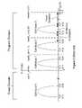
- FIG. 5is a threshold voltage (Vt) distribution graph for a multi-level Flash memory cell.
- the intermediate reference voltagesare also shown.
- This particular graphillustrates the thresholds of a Flash memory cell capable of storing 2 bits of data. Therefore, each multi-level Flash memory cell must store one of four threshold voltages.
- an erased state represented by a negative threshold voltagelies in an erase voltage domain. All erased memory cells will by default have this negative threshold voltage. The remaining three states must be programmed, and their corresponding threshold voltages will be positive in value and lie in the program voltage domain. In this example, the erase voltage domain is below zero while the program voltage domain is above zero volts.
- a problem with this schemeis the required tightness of the distribution for each state and the distance between the states.
- Programmingis typically done by the page, meaning that all the memory cells 50 in the block connected to the same wordline are selected to be programmed with write data (logic “0”) at the same time. The remaining memory cells are thus unselected during programming. Since the memory cells start in the erased state (logic “1”) prior to programming, only the memory cells to be programmed with the logic “0” should be subjected to the high electric fields necessary to promote F-N tunneling. However, due to the physical connections of the memory array, all the memory cells along the same wordline receive the same high voltage programming level. As a result, there is a potential that erased memory cells will have their threshold voltages unintentionally shifted. This is called program disturb, which is well known in the Flash memory field. This problem is more pronounced in multi-level cells as more levels are squeezed into a fixed voltage range.
- Vt windowVt distance
- Vread distanceVt distance
- Vt-stateThe strength or safety margin of a Vt-state is greatest when the Vt is half-way between adjacent reference voltages.
- Upper and lower limits for each Vt-state defining a cell Vt windowmay be specified.
- cell state 0is between lower limit VL 0 ( ⁇ 3 volts) and upper limit VU 0 ( ⁇ 2 volts).
- Cell state 1is between lower limit VL 1 (0.3 volts) and upper limit VU 1 (0.8 volts).
- the cell Vt window in multi-level flash memoryis in between 0.5 to 1.0 volts. Ideally, a narrow cell Vt window is preferred for better definition and distinction of a state.
- the cell Vt distancewhich is defined as the difference in Vt between the lower limit of Vt of the threshold voltage range of one cell state and the upper limit of Vt of the threshold voltage range of the previous cell state.
- the cell Vt distance in a multi-level flash memory cellis in between 0.7 to 1.0V. As is evident, larger cell Vt distances are preferred.
- Vread distancethe distance between the read pass voltage and the upper limit of the fully programmed state as high as possible.
- a lower Vreadis preferred as high Vread can cause disturbance. Therefore, there is a trade-off between Vread distance and the value of Vread.
- the fixed supply-voltage range availablemay determine the maximum Vread value.
- the cell Vt windowbecomes wider by tunnel oxide degradation due to trapped charges.
- the read pass voltage Vreadshould be lower to minimize read disturbance to unselected cells in the selected string.
- the Vread distancehas to be maintained at least well above VU 3 . This increases the level of Vread.
- FIG. 6is a graph illustrating the relationship between the number of program pulses applied to a wordline for programming a threshold voltage versus the size of each pulse.
- tight threshold voltage distributionscan be obtained when the step size of each program pulse is small.
- the trade-offis programming time since more program pulses would be required.
- the data retention characteristic in multi-level cellswill be drastically degraded due to a small cell Vt distance. Moreover, as the Vt distribution for a given state is larger, the maximum Vt of programmed cells is higher. The higher Vt requires a higher programming voltage Vpgm, and adversely affects the data retention characteristics due to the larger electric field across the tunnel oxide. Moreover, the higher Vt required in multi-level cells require higher Vread. This causes read disturbance to unselected memory cells in the selected NAND cell string during read operations (i.e. soft-program by higher Vread to unselected memory cells).
- the life of a multi-level Flash memory cellis relatively short, typically only 10,000 cycles. This is significantly shorter than the 100,000 cycle limit for single bit per cell Flash memory devices.
- present inventionimproves endurance of Flash memory cells by distributing programming threshold voltages in erase and program voltage domains.
- the present inventionprovides a Flash memory device.
- the Flash memory deviceincludes a memory array having memory cells arranged in rows and columns and row control logic.
- the memory arrayhas memory cells arranged in rows and columns, where each memory cell is erasable to have an erase threshold voltage in an erase voltage domain and programmable to have a program threshold voltage in the erase voltage domain.
- the row control logicselectively drive a wordline connected to a gate terminal of a memory cell with one of a positive voltage and a negative voltage during program verify and read operations.
- the Flash memory devicefurther includes a positive voltage generator and a negative voltage generator, where the positive voltage generator provides the positive voltage to the row control logic, and the negative voltage generator provides the negative voltage to the row control logic.
- each memory cellis programmable to have the program threshold voltage in a program voltage domain, and the erase voltage domain includes threshold voltages that are negative while the program voltage domain includes threshold voltages that are positive.
- each memory cellis programmable to store two bits of data corresponding to first, second, third and fourth threshold voltages, where the first threshold voltage and the second threshold voltage are in the erase voltage domain, and the third threshold voltage and the fourth threshold voltage are in the program voltage domain.
- the first threshold voltagecan correspond to the erase threshold voltage.
- the present inventionprovides a method for verifying a threshold voltage of erased memory cells configured in a NAND string.
- the methodincludes precharging a bitline coupled to the NAND string to a first voltage level; applying a reference voltage to all wordlines connected to the erased memory cells of the NAND string for coupling the bitline to a second voltage level; and, sensing a voltage level change in the bitline.
- the first voltage levelis a positive voltage
- the erased memory cellshave an erased threshold voltage in an erase voltage domain while the reference voltage is in the erase voltage domain.
- the reference voltagecan be greater than the erased threshold voltage and less than a programmed threshold voltage in the erase voltage domain.
- the memory cellsare erased if no voltage level change is sensed in the bitline, and the steps of precharging, applying a reference voltage and sensing the memory cells are erased.
- the present inventionprovides a method for programming a Flash memory cell initially erased to have a first threshold voltage in an erase voltage domain.
- the methodincludes changing the first threshold voltage of the Flash memory cell to a second threshold voltage, the second threshold voltage being in the erase voltage domain.
- the step of changingcan include biasing a bitline connected to the Flash memory cell to programming voltage level followed by driving a wordline connected to the Flash memory cell with a predetermined number of pulses, each pulse having a predetermined step size.
- the second threshold voltageis verified and the step of changing is repeated if the Flash memory cell does not have the second threshold voltage.
- the method of verifyingincludes precharging a bitline connected to the Flash memory cell to a first voltage level, driving a wordline connected to the Flash memory cell with a reference voltage in the erase voltage domain, and sensing a voltage level change in the bitline.
- the reference voltagecan be greater than the first threshold voltage and less than the second threshold voltage.
- the Flash memory cell and a plurality of Flash memory cellsform a NAND string, and the step of driving further includes driving wordlines connected to the plurality of Flash memory cells with a pass voltage.
- the present inventionprovides a method for reading a Flash memory cell programmable to have an erase voltage domain threshold voltage or a programming domain threshold voltage.
- the methodincludes determining one of an erase threshold voltage and the erase voltage domain threshold voltage by applying an erase voltage domain reference voltage to a gate terminal of the Flash memory cell and sensing a bitline voltage connected to the Flash memory cell; storing a logical state of the Flash memory cell; determining one of the erase voltage domain threshold voltage and the programming domain threshold voltage by applying another reference voltage to the gate terminal and sensing the bitline voltage connected to the Flash memory cell; and, updating the logical state.
- the present inventionprovides a Flash memory device.
- the Flash memory deviceincludes a memory array having memory cells, each memory cell erasable to have a threshold voltage in an erase voltage domain, and programmable to have at least one threshold voltage level in the erase voltage domain and at least another threshold voltage in a program voltage domain.
- the erase voltage domainincludes threshold voltages that are negative and the program voltage domain includes threshold voltages that are positive, and each memory cell is programmable to store a plurality of bits of data corresponding to first, second, third and fourth threshold voltages.
- the first threshold voltage and the second threshold voltagecan be in the erase voltage domain, and the third threshold voltage and the fourth threshold voltage can be in the program voltage domain.
- the erase voltage domainincludes threshold voltages that are positive and the program voltage domain includes threshold voltages that are negative.
- the Flash memory devicefurther includes row control logic for selectively driving a wordline with a negative voltage and positive voltage in response to a row address.
- the Flash memory devicecan further include a first voltage generator for providing the positive voltage and a second voltage generator for providing the negative voltage.
- the row control logicincludes a row decoder for receiving the positive voltage and the negative voltage, the row decoder providing row signals in response to the row address, and a wordline driver for passing the row signals in response to an enable signal.
- the row control logicincludes a block decoder for providing the enable signal in response to a block address, the enable signal having one of the positive voltage and the negative voltage.
- FIG. 1is a block diagram of a typical Flash memory device
- FIG. 2is a circuit schematic of a NAND cell string
- FIG. 3is a cross-sectional schematic of a typical Flash memory cell
- FIG. 4is a cross-sectional schematic of a nitride ROM cell having charge traps
- FIG. 5is a threshold voltage (Vt) distribution graph for a multi-level Flash memory cell of the prior art
- FIG. 6is a graph illustrating the relationship between the number of program pulses applied to a wordline for programming a threshold voltage versus the size of each pulse;
- FIG. 7is an exemplary embodiment of the invention showing a threshold voltage distribution for a Flash memory cell capable of storing 2 bits of data
- FIG. 8is an alternate embodiment of the invention showing a threshold voltage distribution graph for a Flash memory cell capable of storing 3 bits of data;
- FIG. 9is a block diagram of the row circuits for a multi-level Flash memory device, according to an embodiment of the present invention.
- FIG. 10is a circuit schematic of the block decoder and the wordline driver circuit shown in FIG. 9 ;
- FIG. 11is a circuit schematic of the row decoder circuit shown in FIG. 9 ;
- FIG. 12is a flow chart showing a method for performing an erase-verify operation
- FIG. 13is a flow chart showing a method for programming multiple threshold voltages, according to an embodiment of the present invention.
- FIG. 14is a flow chart showing a program verify method, according to an embodiment of the present invention.
- FIG. 15is a flow chart showing a method for reading data, according to an embodiment of the present invention.
- aspects of the present inventionprovide a threshold voltage distribution scheme for multi-level Flash cells with optimal Vt window and maximum Vt distance, while at the same time maintaining Vread at lower levels. In one embodiment, this is accomplished by programming at least one cell state in the erase voltage domain (for example, with a negative Vt value).
- FIG. 7is an exemplary embodiment of the invention.
- FIG. 7shows a threshold voltage distribution for a multi-level Flash memory cell capable of storing 2 bits of data.
- there is one program state(cell state 1 , corresponding to data “10”) lying in the erased voltage domain with erased state (cell state 0 , corresponding to data “11”). Therefore, there are two cell states lying in the erased voltage domain and two cell states (cell state 2 , corresponding to data “01” and cell state 3 , corresponding to data “00”) in the program voltage domain.
- By programming this state in the erased voltage domaindifferent advantages are obtained. First, endurance is immediately increased relative to the prior art devices having the same Vt window, since the Vt distance between states is increased.
- Vt windowis further increased by minimizing the Vt window, at the expense of programming speed.
- Vt distance and Vt window requirementsare relaxed to provide improved programming performance over prior art devices, but having the same endurance.
- the Vread voltage for unselected cellscan be lowered, for example, from a typical value of 5.5 volts to 4.8 volts.
- FIG. 7shows example values VL and VU values, but any VL and VU can be set for each state.
- the cell state 0has a negative Vt (erase voltage domain) while the remaining three cell states (states 1 , 2 , and 3 ) have positive Vt's (program voltage domain).
- Vterase voltage domain
- state 1 , 2 , and 3program voltage domain
- cell states 0 and 1have negative Vt's
- cell states 2 and 3have positive Vt's.
- the number of cell states in the erase voltage domain and the program voltage domainare equal and hence this scheme is referred to as a “balanced” Vt distribution scheme.
- This balanced cell Vt distribution schemeprovides at least the following advantages: Due to the separation of the cell states, the Vt window of each state can be widened, thus improving the program speed. The cell Vt distance is maximized, which will greatly improve data retention and endurance. This scheme further lowers the program voltage Vpgm and program-pass voltage Vpass, allowing for scaling with device geometry scaling. It also enables lowering of the Vread voltage, which, as a result, provides higher immunity to read disturbance typically encountered by conventional high Vread values. While FIG. 7 is an example Vt distribution for a two bit per cell device, cells storing any number of bits will benefit from the embodiments of the present invention.
- FIG. 8is an alternate embodiment of the invention.
- FIG. 8shows a threshold voltage distribution graph for a multi-level Flash memory cell capable of storing 3 bits of information (i.e. eight different states). It should be noted that in the embodiment of FIG. 8 , exactly half of the eight possible states lie in the erase voltage domain while the other half lies in the program voltage domain. In further alternate embodiments, there can be five states in the erase voltage domain or three states in the erase voltage domain, or other combinations having at least two states in the erase voltage domain.
- ISPPis used for programming desired threshold voltages corresponding to the different states of the multi-level Flash memory cells. As all memory cells are programmed to a desired threshold voltage from the erased state, ISPP gradually shifts the negative threshold voltage of an erased Flash memory cell using increasingly larger voltage pulses applied to its control gate. The incremental step size and number of pulses determines the final threshold voltage of the programmed Flash memory cell.
- a programmed state in the erase voltage domainis achieved by setting the number of pulses and step size of the pulses such that the desired negative threshold voltage is obtained. In the example of FIG. 6 , a ⁇ 2V threshold voltage is obtained by using between 2 and 3 pulses, depending on the selected pulse step size.
- the remaining program domain statesare programmed according to known techniques. It is noted that the step size for programming the erase domain states can be small without impacting programming speed since the threshold voltage shift from the erase state is relatively small.
- a part of any programming operationis the program verify operation, which is used to check that the data has been properly programmed.
- the desired threshold voltagemay not have been set during a program operation. Therefore, the memory cell(s) is subjected to reprogramming until the program verify clears the memory cell, or until it is determined that the cell is defective. Once the program verify operation clears the memory cells, the data can be read.
- program verify and read operationsare executed with both positive and negative voltages.
- Table 1shows bias conditions of the selected wordline and unselected wordlines to distinguish each cell state during read, verify & control programmed cell Vt during program in a conventional multi-level flash memory using the cell Vt distribution scheme of FIG. 5 .
- Table 2shows bias conditions of the selected wordline and unselected wordlines during program verify and read in a multi-level flash memory programmable to have at least two states in the erase voltage domain, according to an aspect of the present invention.
- Table 2shows exemplary bias conditions for the program verify and read operations used for a multi-level Flash cell programmable to have at least two states in the erase voltage domain. As illustrated in Table 2, the negative voltages are applied to the selected wordline during the read and program verify operations for cells having negative cell Vt (i.e. cell state 0 and cell state 1 ). It should be noted that the voltage values in Table 2 are for illustration purpose only. In other words, voltage values in Table 2 can be varied according to process technology and cell characteristics.
- the program verify voltage and read voltage applied to the selected wordlinesare different from conventional program verify and read operations, as shown in Table 2.
- all program verify voltage and read voltageare implemented with positive voltage values.
- the threshold voltage distribution scheme for multi-level Flash cells described hereinutilizes both positive and negative voltages for program verify and read operations. This results in changes to the implementation for the wordline circuits as described below.
- FIG. 9is a block diagram of an exemplary row control logic for a multi-level Flash memory device according to an embodiment of the present invention.
- the row control logic 100includes a block decoder 102 , a row decoder circuit 108 and a wordline driver circuit 110 .
- the device having row control logic 100has a high voltage generator 104 and a negative voltage generator 106 , which may be used by other circuits that are not shown in FIG. 9 .
- the row decoder 108is commonly shared among all memory blocks, which receives a row address RA_b, as well as other signals which are not shown, for generating the source select signal SS, wordline signals S[ 0 :n], and the ground select signal GS, generically referred to as row signals. Since at least one of the programmed states will be in the erase voltage domain (with a negative threshold voltage for example), the block decoder 102 and the row decoder circuit 108 will receive one or more negative voltages for application to a selected wordline signal. In response to a valid block address BA and row decoder signals, signals SSL, GSL and WL 0 -WLn are set to their required voltage levels during program, program verify and read operations. Example voltages are shown in Table 2 for program verify and read operations.
- FIG. 10is a circuit schematic showing circuit details of the block decoder 102 and wordline driver circuit 110 of FIG. 9 .
- Block decoder 102is associated with one memory block, and includes a cross coupled inverter latch circuit and level shifter circuit.
- the latch circuitincludes cross-coupled inverters 200 and 202 , an n-channel reset transistor 204 , and n-channel enable transistors 206 and 208 .
- the latch circuitis enabled, or set, when latch enable signal LTCH_EN and a block address BA are at the high logic level.
- the latch circuit of inverters 200 and 202is reset when signal RST_BD is at the high logic level.
- the level shifter circuitincludes a pair of cross-coupled p-channel transistors 210 and 212 , each being connected to respective n-channel steering transistors 214 and 216 .
- the shared terminals of transistors 210 and 212receives a high voltage Vh while the shared terminals of transistors 214 and 216 receives a negative voltage Vn.
- Node Vhis connected to the positive voltage generator 104 while node Vn is connected to the negative voltage generator 106 .
- Steering transistors 214 and 216have gate terminals connected to the output of inverter 200 and inverter 218 , the input of which is connected to the gate of transistor 214 .
- the output of the level shifter circuit (an enabling signal) BD_outdrives the gate terminals of all the n-channel pass transistors 220 of wordline drivers 110 .
- the substrate terminal of all the pass transistors 220are connected to Vn.
- Each pass transistorcan selectively pass the source select (SS), wordline (S 0 -Sn) and ground select (GS) signals to the memory array.
- Placeholder “n”can be any non-zero integer number, typically corresponding to the maximum number of cells in the Flash cell string.
- one memory blockis selected while other blocks remain unselected. In otherwords, one memory block is enabled while remaining memory blocks are disabled. To enable a memory block, LTCH_EN and BA will be at the high logic level, thereby setting the level shifter circuit to output high voltage Vh. Therefore, all the pass transistors 220 of wordline driver circuit 110 are turned on. Unselected wordlines (unselected Si) will be set to a Vread voltage while the selected wordline (selected Si) will be set to the desired voltage. The desired voltage can be ⁇ 1.5V if the present read operation is intended to distinguish between cell state 0 and cell state 1 , for example.
- Disabled memory blockswill have their corresponding block decoder circuit output set to output low voltage Vn ( ⁇ 1.5V for example). Therefore, all the pass transistors 220 in the unselected memory blocks will be turned off even though one of the Si signals may be at Vn of ⁇ 1.5V for example.
- Table 3illustrates example Vh and Vn voltages for read, program, program verify, erase and erase verify operations.
- FIG. 11is a circuit schematic showing one row decoder circuit of row decoder 108 of FIG. 9 .
- the presently shown schematic of FIG. 11is a functional representation only, as there can be different specific circuit implementations that are possible.
- program voltage domainie. positive voltages
- erase voltage domainie. negative voltages
- FIG. 11shows one circuit for generating one row signal Si where i can be an integer value between 0 and n, but the circuits for generating signals SS and GS are similarly configured.
- the row decoder circuitincludes a multiplexor 300 for receiving all the voltages that are used during program, program verify, read, erase and erase verify operations. This includes for example, a program verify voltage Vver, a read voltage Vread, a pass voltage Vpass, and a programming voltage Vpgm.
- Multiplexor 300further receives the different reference voltages used for read and program verify operations, such as Vref_rd 1 , Vref_rd 2 and Vref_rd 3 for the 2 bit/cell configuration.
- Vref_rd 1is a negative erase domain voltage
- Vref_rd 2 and Vref_rd 3are positive program domain voltages.
- Any number of voltagescan be provided to multiplexor 300 , and then selectively passed to node Sn.
- Voltage selection signal Vselectis used to pass any one of the voltages. Those skilled in the art will understand that Vselect will be a multi-bit signal, the number depending on the number of input ports that multiplexor 300 is configured to have.
- the row decoder circuitincludes an n-channel disabling transistor 302 connected between node Sn and ground for disabling the circuit when not in use, or during a power down mode of operation, for example.
- signal Snis enabled in response to a selected address for enabling a particular wordline when address RA_b is at the low logic level.
- RA_bcan be a decoded row address or a predecoded row address.
- Vselectwill be set to pass one of the voltages received by multiplexor 300 to the Sn node.
- the voltage generators 104 and 106 of FIG. 9are controlled to provide the appropriate voltage levels depending on the operation being performed.
- Table 4illustrates example voltages applied to the wordlines and by the row decoder circuit during a read operation for selected and unselected wordlines Si, where i is an integer value between 0 and n.
- Table 5illustrates example voltages applied to the wordlines and by the row decoder circuit during a program verify operation for selected and unselected wordlines Si, where i is an integer value between 0 and n.
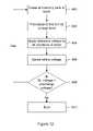
- FIG. 12is a flow chart showing a method for performing an erase verify operation according to an embodiment of the present invention. Since a programmed state will be in the erase voltage domain, the method of FIG. 12 ensures that all the memory cells are sufficiently erased such that their threshold voltages do not lie within the designated negative threshold voltage range for a programmed state.
- the method of FIG. 12commences at step 400 by erasing a selected block of the memory array. After all the memory cells have been erased, all the bitlines of the selected memory block are precharged to a first voltage level such as VDD at step 402 . A reference voltage is then applied to all the wordlines of the memory cells at step 404 . It is presumed that the memory cells are configured as NAND cell strings, such as the ones previously shown in FIG. 2 . The reference voltage is selected to be greater than the highest possible erase threshold voltage for the erase state, and lower than the lowest possible program threshold voltage for the adjacent program state. Generally, the reference voltage in the erase domain voltage, and in the example where the erase domain is below 0V, the reference voltage is a negative voltage level.
- the threshold voltageshould be between ⁇ 2.9 and ⁇ 2.1 volts.
- the reference voltage applied to the wordlineswill be about ⁇ 1.5 volts. If all the memory cells have been properly erased, then the ⁇ 1.5 volt level on wordlines 0 to 31 is sufficient to turn on the transistors and discharge the bitline to CSL or ground. However, if any one of the cells in the NAND cell string has a threshold voltage higher than ⁇ 1.5 volts, then the bitline will not discharge to ground. Therefore, the bitline voltage is sensed at step 406 .
- bitline voltageis equal or not to the original pre-charge voltage. If the bitline voltage is the same, then the method loops back to step 400 to re-erase the cells and repeat the verification process. Otherwise, all the memory cells have been properly erased and the erase verify method ends at step 410 .
- FIG. 13is a flow chart illustrating a method of programming one programmed state in the erase voltage domain, according to an embodiment of the present invention.
- the methodstarts at step 500 by setting the ISPP parameters such as number of program pulses and step size for each pulse, for the state to be programmed in the erase voltage domain.
- the erase voltage domain threshold voltageis programmed to the selected Flash memory cells.
- the erase threshold voltage of a memory cellis effectively shifted to the desired erase domain threshold voltage level by using a predetermined number of program pulses and step sizes in accordance with the ISPP scheme.
- a program verify operationis executed to ensure that the programmed state has been properly programmed. More specifically, the program verify will use the appropriate erase voltage domain reference voltage to verify the programmed state. In the present example, the program verify reference voltage will be a negative voltage level. Further details of the program verify operation are shown later in FIG. 14 .
- the remaining statescan include further erase voltage domain states and/or program voltage domain states. Further erase voltage domain states are programmed according to the same sequence shown in steps 500 to 506 , but with different ISPP parameters and program verify reference voltages.
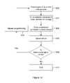
- FIG. 14is a flow chart of a method for performing a program verify operation after a state has been programmed in the erase voltage domain.
- the methodstarts at step 600 by precharging the bitlines to a first voltage level, such as positive voltage level for example.
- the selected wordline corresponding to the page that was programmedis driven to an erase voltage domain reference voltage, and unselected wordlines are driven to a read voltage at step 604 .
- the erase voltage domain reference voltageis selected to be lower than the desired threshold voltage range of the currently programmed state, but higher than the adjacent state having a lower threshold voltage range. In the example of FIG. 7 , if the programmed state being verified is cell state 1 , then the erase voltage domain reference voltage is selected to be higher than Vref 1 -rd.
- the read voltageis typically a program voltage domain voltage sufficient to turn on a memory cell having the highest programmed threshold voltage, such as Vread in the example of FIG. 7 .
- the bitlineis sensed at step 606 , and a determination is made at step 608 to see if the bitline voltage has changed, ie. been discharged through the NAND cell string. If there is a change to the bitline voltage, then the threshold voltage of the currently programmed state is too low and conducts current. Thus the memory cell(s) are deemed to have failed, and the method proceeds to step 610 to repeat programming for the failed cell(s). Otherwise, the program verify method ends at step 612 as all the cells have passed verification for the currently programmed state.
- latches for the two bits representing one of four possible logic statesare set to default states, such as 1,1 for example. Reading is accomplished by iteratively reading out the cell by applying Vref 1 -rd, Vref 2 -rd and Vref 3 -rd in each iteration. If the threshold voltage of the selected memory cell is determined to be less than the applied reference voltage for that iteration, then neither bit state is changed, or toggled. If the threshold voltage of the selected memory cell is determined to be greater than the applied reference voltage for that iteration, then one bit state is changed, or toggled. The particular bit to toggle depends on the specific read iteration being executed. This ensures that the bit states for the lowest threshold voltage (ie. erased state) will remain unchanged for each subsequent iteration. Hence, for a two bit multi-level memory cell, three read iterations are required for determining the two bit state of the memory cell.
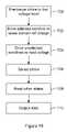
- FIG. 15is a flow chart of a method for reading one cell state in the erase voltage domain.
- the methodstarts at step 700 by precharging the bitlines to a first voltage level, such as a positive voltage level for example.
- the selected wordlineis driven to an erase voltage domain reference voltage at step 702 , while the remaining unselected wordlines are driven to a read voltage at step 704 .
- the erase voltage domain reference voltageis selected to be lower than the desired threshold voltage range of the currently programmed state, but higher than the adjacent state having a lower threshold voltage range.
- the erase voltage domain reference voltageis selected to be Vref 1 -rd.
- the read voltageis typically a program voltage domain voltage sufficient to turn on a memory cell having the highest programmed threshold voltage, such as Vread in the example of FIG. 8 .
- the bitlineis sensed at step 706 to determine if the cell threshold voltage is either greater than or less than Vref 1 -rd, and the states of the bits are updated.
- the remaining statesare sensed to complete the read operation for the memory cell.
- the remaining statescan be further erase voltage domain states and program voltage domain states.
- the read processwill repeat with the updated parameters corresponding to the state being sensed, ie, setting the reference voltage to Vref 2 -rd at step 700 .
- the multi-bit logic states corresponding to the threshold level stored in the memory cellare output through read path circuits at step 710 .
- the erase voltage domainis described in the example embodiments as being voltages less than 0V while the program voltage domain include voltages greater than 0V.
- the threshold voltage distribution schemecan be inverted, such that the erase voltage domain includes voltages greater than 0V while the program voltage domain includes voltages less than 0V.
- Embodiments of the inventioncan be represented as a software product stored in a machine-readable medium (also referred to as a computer-readable medium, a processor-readable medium, or a computer usable medium having a computer-readable program code embodied therein).
- the machine-readable mediumcan be any suitable tangible medium, including magnetic, optical, or electrical storage medium including a diskette, compact disk read only memory (CD-ROM), memory device (volatile or non-volatile), or similar storage mechanism.
- the machine-readable mediumcan contain various sets of instructions, code sequences, configuration information, or other data, which, when executed, cause a processor to perform steps in a method according to an embodiment of the invention.
- Those of ordinary skill in the artwill appreciate that other instructions and operations necessary to implement the described invention can also be stored on the machine-readable medium.
- Software running from the machine-readable mediumcan interface with circuitry to perform the described tasks.
Landscapes
- Engineering & Computer Science (AREA)
- Computer Hardware Design (AREA)
- Microelectronics & Electronic Packaging (AREA)
- Read Only Memory (AREA)
Abstract
Description
| TABLE 1 | |||
| Program Verify | Read | ||
| Selected | Unselected | Selected | Unselected | ||
| Wordline | Wordlines | Wordline | |||
| Cell State |
0 | 0.3 V (Vref_pv1) | 5.5 V (Vread) | 0 V (Vref_rd1) | 5.5 V (Vread) |
| 1.5 V (Vref_pv2) | 5.5 V (Vread) | 1.1 V (Vref_rd2) | 5.5 V (Vread) |
| 2.8 V (Vref_pv3) | 5.5 V (Vread) | 2.3 V (Vref_rd3) | 5.5 V (Vread) |
| TABLE 2 | |||
| Program Verify | Read | ||
| Selected | Unselected | Selected | Unselected | ||
| Wordline | Wordlines | Wordline | |||
| Cell State |
| 0 | −1.1 V (Vref_pv1) | 4.8 V (Vread) | −1.5 V (Vref_rd1) | 4.8 V (Vread) |
| 0.5 V (Vref_pv2) | 4.8 V (Vread) | 0 V (Vref_rd2) | 4.8 V (Vread) |
| 2.1 V (Vref_pv3) | 4.8 V (Vread) | 1.5 V (Vref_rd3) | 4.8 V (Vread) |
| TABLE 3 | |||
| Vh | Vn | ||
| Read | ~6.5 | 0 V/−1.5 V (Vref_rd1) | ||
| Program | ~18 | 0 V | ||
| Program Verify | ~6.5 | 0 V/−1.1 V (Vref_pv1) | ||
| Erase | 0 V | |||
| Erase Verify | ~6.5 | 0 V | ||
| TABLE 4 | |||
| Cell | Cell | ||
| Signal | State | ||
| 1 | | | |
| Unselected | −1.5 V | −1.5 V or 0 V | −1.5 V or 0 V |
| BD_out | |||
| (Unselected | |||
| Block) | |||
| Selected | 6.5 V | 6.5 V | 6.5 V |
| BD_out | |||
| (Selected | |||
| Block) | |||
| Vh | 6.5 V | 6.5 V | 6.5 V |
| Vn | −1.5 V | −1.5 V or 0 V | −1.5 V or 0 V |
| SS | 4.8 V (Vread) | 4.8 V (Vread) | 4.8 V (Vread) |
| Selected Si | −1.5 V (Vref_rd1) | 0 V | 1.5 V |
| (Vref_rd2) | (Vref_rd3) | ||
| Unselected | 4.8 V (Vread) | 4.8 V (Vread) | 4.8 V (Vread) |
| Si | |||
| GS | 4.8 V (Vread) | 4.8 V (Vread) | 4.8 V (Vread) |
| TABLE 5 | ||||
| Cell State | 1 | | | |
| Unselected | −1.1 V | −1.1 V or 0 V | −1.1 V or 0 V | |
| BD_out | ||||
| (Unselected | ||||
| Block) | ||||
| Selected | 6.5 V | 6.5 V | 6.5 V | |
| BD_out | ||||
| (Selected | ||||
| Block) | ||||
| Vh | 6.5 V | 6.5 V | 6.5 V | |
| Vn | −1.1 V | 0.5 V or 0 V | 2.1 V or 0 V | |
| SS | 4.8 V (Vread) | 4.8 V (Vread) | 4.8 V (Vread) | |
| Selected Si | −1.1 V (Vref_pv1) | 0.5 V | 2.1 V | |
| (Vref_pv2) | (Vref_pv3) | |||
| Unselected | 4.8 V (Vread) | 4.8 V (Vread) | 4.8 V (Vread) | |
| Si | ||||
| GS | 4.8 V (Vread) | 4.8 V (Vread) | 4.8 V (Vread) | |
Claims (16)
Priority Applications (6)
| Application Number | Priority Date | Filing Date | Title |
|---|---|---|---|
| US11/762,330US7593259B2 (en) | 2006-09-13 | 2007-06-13 | Flash multi-level threshold distribution scheme |
| US12/463,759US7821827B2 (en) | 2006-09-13 | 2009-05-11 | Flash multi-level threshold distribution scheme |
| US12/884,939US8102708B2 (en) | 2006-09-13 | 2010-09-17 | Flash multi-level threshold distribution scheme |
| US13/328,762US8462551B2 (en) | 2006-09-13 | 2011-12-16 | Flash multi-level threshold distribution scheme |
| US13/892,743US8711621B2 (en) | 2006-09-13 | 2013-05-13 | Flash multi-level threshold distribution scheme |
| US14/208,812US9263146B2 (en) | 2006-09-13 | 2014-03-13 | Flash multi-level threshold distribution scheme |
Applications Claiming Priority (2)
| Application Number | Priority Date | Filing Date | Title |
|---|---|---|---|
| US84415406P | 2006-09-13 | 2006-09-13 | |
| US11/762,330US7593259B2 (en) | 2006-09-13 | 2007-06-13 | Flash multi-level threshold distribution scheme |
Related Child Applications (1)
| Application Number | Title | Priority Date | Filing Date |
|---|---|---|---|
| US12/463,759ContinuationUS7821827B2 (en) | 2006-09-13 | 2009-05-11 | Flash multi-level threshold distribution scheme |
Publications (2)
| Publication Number | Publication Date |
|---|---|
| US20080062760A1 US20080062760A1 (en) | 2008-03-13 |
| US7593259B2true US7593259B2 (en) | 2009-09-22 |
Family
ID=39183317
Family Applications (6)
| Application Number | Title | Priority Date | Filing Date |
|---|---|---|---|
| US11/762,330Active2028-01-01US7593259B2 (en) | 2006-09-13 | 2007-06-13 | Flash multi-level threshold distribution scheme |
| US12/463,759ActiveUS7821827B2 (en) | 2006-09-13 | 2009-05-11 | Flash multi-level threshold distribution scheme |
| US12/884,939ActiveUS8102708B2 (en) | 2006-09-13 | 2010-09-17 | Flash multi-level threshold distribution scheme |
| US13/328,762ActiveUS8462551B2 (en) | 2006-09-13 | 2011-12-16 | Flash multi-level threshold distribution scheme |
| US13/892,743ActiveUS8711621B2 (en) | 2006-09-13 | 2013-05-13 | Flash multi-level threshold distribution scheme |
| US14/208,812ActiveUS9263146B2 (en) | 2006-09-13 | 2014-03-13 | Flash multi-level threshold distribution scheme |
Family Applications After (5)
| Application Number | Title | Priority Date | Filing Date |
|---|---|---|---|
| US12/463,759ActiveUS7821827B2 (en) | 2006-09-13 | 2009-05-11 | Flash multi-level threshold distribution scheme |
| US12/884,939ActiveUS8102708B2 (en) | 2006-09-13 | 2010-09-17 | Flash multi-level threshold distribution scheme |
| US13/328,762ActiveUS8462551B2 (en) | 2006-09-13 | 2011-12-16 | Flash multi-level threshold distribution scheme |
| US13/892,743ActiveUS8711621B2 (en) | 2006-09-13 | 2013-05-13 | Flash multi-level threshold distribution scheme |
| US14/208,812ActiveUS9263146B2 (en) | 2006-09-13 | 2014-03-13 | Flash multi-level threshold distribution scheme |
Country Status (9)
| Country | Link |
|---|---|
| US (6) | US7593259B2 (en) |
| EP (2) | EP2064707B1 (en) |
| JP (2) | JP2010503944A (en) |
| KR (3) | KR101515645B1 (en) |
| CN (2) | CN101517652B (en) |
| CA (1) | CA2659872A1 (en) |
| ES (2) | ES2404831T3 (en) |
| TW (2) | TWI462102B (en) |
| WO (1) | WO2008031217A1 (en) |
Cited By (92)
| Publication number | Priority date | Publication date | Assignee | Title |
|---|---|---|---|---|
| US20080126686A1 (en)* | 2006-11-28 | 2008-05-29 | Anobit Technologies Ltd. | Memory power and performance management |
| US20080130341A1 (en)* | 2006-12-03 | 2008-06-05 | Anobit Technologies Ltd. | Adaptive programming of analog memory |
| US20080181001A1 (en)* | 2007-01-24 | 2008-07-31 | Anobit Technologies | Memory device with negative thresholds |
| US20090091979A1 (en)* | 2007-10-08 | 2009-04-09 | Anobit Technologies | Reliable data storage in analog memory cells in the presence of temperature variations |
| US20090213654A1 (en)* | 2008-02-24 | 2009-08-27 | Anobit Technologies Ltd | Programming analog memory cells for reduced variance after retention |
| US20090303799A1 (en)* | 2008-06-10 | 2009-12-10 | Kabushiki Kaisha Toshiba | Non-volatile semiconductor memory device and erasing method thereof |
| US7697326B2 (en) | 2006-05-12 | 2010-04-13 | Anobit Technologies Ltd. | Reducing programming error in memory devices |
| US20100110787A1 (en)* | 2006-10-30 | 2010-05-06 | Anobit Technologies Ltd. | Memory cell readout using successive approximation |
| US20100174854A1 (en)* | 2007-02-16 | 2010-07-08 | Mosaid Technologies Incorporated | Non-volatile memory with dynamic multi-mode operation |
| US7900102B2 (en) | 2006-12-17 | 2011-03-01 | Anobit Technologies Ltd. | High-speed programming of memory devices |
| US7925936B1 (en) | 2007-07-13 | 2011-04-12 | Anobit Technologies Ltd. | Memory device with non-uniform programming levels |
| US7924613B1 (en) | 2008-08-05 | 2011-04-12 | Anobit Technologies Ltd. | Data storage in analog memory cells with protection against programming interruption |
| US7924587B2 (en) | 2008-02-21 | 2011-04-12 | Anobit Technologies Ltd. | Programming of analog memory cells using a single programming pulse per state transition |
| US20110141822A1 (en)* | 2009-12-14 | 2011-06-16 | Ercole Rosario Di Iorio | Source Bias Shift for Multilevel Memories |
| US7975192B2 (en) | 2006-10-30 | 2011-07-05 | Anobit Technologies Ltd. | Reading memory cells using multiple thresholds |
| US7995388B1 (en) | 2008-08-05 | 2011-08-09 | Anobit Technologies Ltd. | Data storage using modified voltages |
| US8000135B1 (en) | 2008-09-14 | 2011-08-16 | Anobit Technologies Ltd. | Estimation of memory cell read thresholds by sampling inside programming level distribution intervals |
| US8001320B2 (en) | 2007-04-22 | 2011-08-16 | Anobit Technologies Ltd. | Command interface for memory devices |
| US8000141B1 (en) | 2007-10-19 | 2011-08-16 | Anobit Technologies Ltd. | Compensation for voltage drifts in analog memory cells |
| US20110249493A1 (en)* | 2008-10-10 | 2011-10-13 | Kabushiki Kaisha Toshiba | Nand flash memory |
| US8050086B2 (en) | 2006-05-12 | 2011-11-01 | Anobit Technologies Ltd. | Distortion estimation and cancellation in memory devices |
| US8060806B2 (en) | 2006-08-27 | 2011-11-15 | Anobit Technologies Ltd. | Estimation of non-linear distortion in memory devices |
| US8059457B2 (en) | 2008-03-18 | 2011-11-15 | Anobit Technologies Ltd. | Memory device with multiple-accuracy read commands |
| US8068360B2 (en) | 2007-10-19 | 2011-11-29 | Anobit Technologies Ltd. | Reading analog memory cells using built-in multi-threshold commands |
| US8085586B2 (en) | 2007-12-27 | 2011-12-27 | Anobit Technologies Ltd. | Wear level estimation in analog memory cells |
| US8151166B2 (en) | 2007-01-24 | 2012-04-03 | Anobit Technologies Ltd. | Reduction of back pattern dependency effects in memory devices |
| US8151163B2 (en) | 2006-12-03 | 2012-04-03 | Anobit Technologies Ltd. | Automatic defect management in memory devices |
| US8156398B2 (en) | 2008-02-05 | 2012-04-10 | Anobit Technologies Ltd. | Parameter estimation based on error correction code parity check equations |
| US8156403B2 (en) | 2006-05-12 | 2012-04-10 | Anobit Technologies Ltd. | Combined distortion estimation and error correction coding for memory devices |
| US8169825B1 (en) | 2008-09-02 | 2012-05-01 | Anobit Technologies Ltd. | Reliable data storage in analog memory cells subjected to long retention periods |
| US8174905B2 (en) | 2007-09-19 | 2012-05-08 | Anobit Technologies Ltd. | Programming orders for reducing distortion in arrays of multi-level analog memory cells |
| US8174857B1 (en) | 2008-12-31 | 2012-05-08 | Anobit Technologies Ltd. | Efficient readout schemes for analog memory cell devices using multiple read threshold sets |
| US8208304B2 (en) | 2008-11-16 | 2012-06-26 | Anobit Technologies Ltd. | Storage at M bits/cell density in N bits/cell analog memory cell devices, M>N |
| US8209588B2 (en) | 2007-12-12 | 2012-06-26 | Anobit Technologies Ltd. | Efficient interference cancellation in analog memory cell arrays |
| US20120176844A1 (en)* | 2011-01-06 | 2012-07-12 | Cunningham Jeffrey C | Read conditions for a non-volatile memory (nvm) |
| US8225181B2 (en) | 2007-11-30 | 2012-07-17 | Apple Inc. | Efficient re-read operations from memory devices |
| US8228701B2 (en) | 2009-03-01 | 2012-07-24 | Apple Inc. | Selective activation of programming schemes in analog memory cell arrays |
| US8230300B2 (en) | 2008-03-07 | 2012-07-24 | Apple Inc. | Efficient readout from analog memory cells using data compression |
| US8234545B2 (en) | 2007-05-12 | 2012-07-31 | Apple Inc. | Data storage with incremental redundancy |
| US8238157B1 (en) | 2009-04-12 | 2012-08-07 | Apple Inc. | Selective re-programming of analog memory cells |
| US8239735B2 (en) | 2006-05-12 | 2012-08-07 | Apple Inc. | Memory Device with adaptive capacity |
| US8239734B1 (en) | 2008-10-15 | 2012-08-07 | Apple Inc. | Efficient data storage in storage device arrays |
| US8248831B2 (en) | 2008-12-31 | 2012-08-21 | Apple Inc. | Rejuvenation of analog memory cells |
| US8254167B2 (en) | 2010-05-17 | 2012-08-28 | Seagate Technologies Llc | Joint encoding of logical pages in multi-page memory architecture |
| US8261159B1 (en) | 2008-10-30 | 2012-09-04 | Apple, Inc. | Data scrambling schemes for memory devices |
| US8259497B2 (en) | 2007-08-06 | 2012-09-04 | Apple Inc. | Programming schemes for multi-level analog memory cells |
| US8259506B1 (en) | 2009-03-25 | 2012-09-04 | Apple Inc. | Database of memory read thresholds |
| US8270246B2 (en) | 2007-11-13 | 2012-09-18 | Apple Inc. | Optimized selection of memory chips in multi-chips memory devices |
| US8320185B2 (en) | 2010-03-31 | 2012-11-27 | Micron Technology, Inc. | Lifetime markers for memory devices |
| US8369141B2 (en) | 2007-03-12 | 2013-02-05 | Apple Inc. | Adaptive estimation of memory cell read thresholds |
| US8400858B2 (en) | 2008-03-18 | 2013-03-19 | Apple Inc. | Memory device with reduced sense time readout |
| US8406051B2 (en) | 2010-05-17 | 2013-03-26 | Seagate Technology Llc | Iterative demodulation and decoding for multi-page memory architecture |
| US8429493B2 (en) | 2007-05-12 | 2013-04-23 | Apple Inc. | Memory device with internal signap processing unit |
| US20130111130A1 (en)* | 2011-11-01 | 2013-05-02 | Edward M. McCombs | Memory including a reduced leakage wordline driver |
| US8479080B1 (en) | 2009-07-12 | 2013-07-02 | Apple Inc. | Adaptive over-provisioning in memory systems |
| US8482978B1 (en) | 2008-09-14 | 2013-07-09 | Apple Inc. | Estimation of memory cell read thresholds by sampling inside programming level distribution intervals |
| US8495465B1 (en) | 2009-10-15 | 2013-07-23 | Apple Inc. | Error correction coding over multiple memory pages |
| US8526266B2 (en) | 2011-01-21 | 2013-09-03 | Qualcomm Incorporated | Row-decoder circuit and method with dual power systems |
| US8527819B2 (en) | 2007-10-19 | 2013-09-03 | Apple Inc. | Data storage in analog memory cell arrays having erase failures |
| US8559229B2 (en) | 2010-09-30 | 2013-10-15 | Samsung Electronics Co., Ltd. | Flash memory device and wordline voltage generating method thereof |
| US8572423B1 (en) | 2010-06-22 | 2013-10-29 | Apple Inc. | Reducing peak current in memory systems |
| US8572311B1 (en) | 2010-01-11 | 2013-10-29 | Apple Inc. | Redundant data storage in multi-die memory systems |
| US8595591B1 (en) | 2010-07-11 | 2013-11-26 | Apple Inc. | Interference-aware assignment of programming levels in analog memory cells |
| US8645794B1 (en) | 2010-07-31 | 2014-02-04 | Apple Inc. | Data storage in analog memory cells using a non-integer number of bits per cell |
| US8677054B1 (en) | 2009-12-16 | 2014-03-18 | Apple Inc. | Memory management schemes for non-volatile memory devices |
| US8694814B1 (en) | 2010-01-10 | 2014-04-08 | Apple Inc. | Reuse of host hibernation storage space by memory controller |
| US8693257B2 (en) | 2011-10-18 | 2014-04-08 | Seagate Technology Llc | Determining optimal read reference and programming voltages for non-volatile memory using mutual information |
| US8694854B1 (en) | 2010-08-17 | 2014-04-08 | Apple Inc. | Read threshold setting based on soft readout statistics |
| US8694853B1 (en) | 2010-05-04 | 2014-04-08 | Apple Inc. | Read commands for reading interfering memory cells |
| US8705273B2 (en) | 2010-12-20 | 2014-04-22 | Samsung Electronics Co., Ltd. | Negative voltage generator, decoder, nonvolatile memory device and memory system using negative voltage |
| US8711619B2 (en) | 2011-10-18 | 2014-04-29 | Seagate Technology Llc | Categorizing bit errors of solid-state, non-volatile memory |
| US8737133B2 (en) | 2011-10-18 | 2014-05-27 | Seagate Technology Llc | Shifting cell voltage based on grouping of solid-state, non-volatile memory cells |
| US8760932B2 (en) | 2011-10-18 | 2014-06-24 | Seagate Technology Llc | Determination of memory read reference and programming voltages |
| US8832354B2 (en) | 2009-03-25 | 2014-09-09 | Apple Inc. | Use of host system resources by memory controller |
| US8856475B1 (en) | 2010-08-01 | 2014-10-07 | Apple Inc. | Efficient selection of memory blocks for compaction |
| US8924661B1 (en) | 2009-01-18 | 2014-12-30 | Apple Inc. | Memory system including a controller and processors associated with memory devices |
| US8949684B1 (en) | 2008-09-02 | 2015-02-03 | Apple Inc. | Segmented data storage |
| US20150082121A1 (en)* | 2013-09-18 | 2015-03-19 | Lsi Corporation | Method of erase state handling in flash channel tracking |
| US9021181B1 (en) | 2010-09-27 | 2015-04-28 | Apple Inc. | Memory management for unifying memory cell conditions by using maximum time intervals |
| US9104580B1 (en) | 2010-07-27 | 2015-08-11 | Apple Inc. | Cache memory for hybrid disk drives |
| US9135109B2 (en) | 2013-03-11 | 2015-09-15 | Seagate Technology Llc | Determination of optimum threshold voltage to read data values in memory cells |
| US9412450B2 (en) | 2013-02-27 | 2016-08-09 | Samsung Electronics Co., Ltd. | Three-dimensional nonvolatile memory and operating method of three-dimensional nonvolatile memory |
| US9928126B1 (en) | 2017-06-01 | 2018-03-27 | Apple Inc. | Recovery from cross-temperature read failures by programming neighbor word lines |
| US10163523B2 (en)* | 2015-03-31 | 2018-12-25 | SK Hynix Inc. | Semiconductor device and operating method thereof |
| US20190074060A1 (en)* | 2014-01-09 | 2019-03-07 | Micron Technology, Inc. | Memory Systems and Memory Programming Methods |
| US10468096B2 (en) | 2012-10-15 | 2019-11-05 | Seagate Technology Llc | Accelerated soft read for multi-level cell nonvolatile memories |
| US11189355B1 (en) | 2020-08-25 | 2021-11-30 | Micron Technology, Inc. | Read window based on program/erase cycles |
| US11392312B2 (en) | 2020-08-25 | 2022-07-19 | Micron Technology, Inc. | Read calibration based on ranges of program/erase cycles |
| US11430528B2 (en) | 2020-08-25 | 2022-08-30 | Micron Technology, Inc. | Determining a read voltage based on a change in a read window |
| US11556416B2 (en) | 2021-05-05 | 2023-01-17 | Apple Inc. | Controlling memory readout reliability and throughput by adjusting distance between read thresholds |
| US11776629B2 (en) | 2020-08-17 | 2023-10-03 | Micron Technology, Inc. | Threshold voltage based on program/erase cycles |
| US11847342B2 (en) | 2021-07-28 | 2023-12-19 | Apple Inc. | Efficient transfer of hard data and confidence levels in reading a nonvolatile memory |
Families Citing this family (58)
| Publication number | Priority date | Publication date | Assignee | Title |
|---|---|---|---|---|
| US7593259B2 (en)* | 2006-09-13 | 2009-09-22 | Mosaid Technologies Incorporated | Flash multi-level threshold distribution scheme |
| KR100888842B1 (en)* | 2007-06-28 | 2009-03-17 | 삼성전자주식회사 | Flash memory device that can optimize the read voltage and how to set its read voltage |
| US7639532B2 (en)* | 2007-10-10 | 2009-12-29 | Micron Technology, Inc. | Non-equal threshold voltage ranges in MLC NAND |
| US7633798B2 (en)* | 2007-11-21 | 2009-12-15 | Micron Technology, Inc. | M+N bit programming and M+L bit read for M bit memory cells |
| KR101458955B1 (en)* | 2008-01-04 | 2014-11-10 | 삼성전자주식회사 | Program verification method of flash memory device to obtain wide pass voltage window |
| IT1391466B1 (en)* | 2008-07-09 | 2011-12-23 | Micron Technology Inc | DETECTION OF A MEMORY CELL THROUGH NEGATIVE VOLTAGE |
| US7852671B2 (en) | 2008-10-30 | 2010-12-14 | Micron Technology, Inc. | Data path for multi-level cell memory, methods for storing and methods for utilizing a memory array |
| KR101596826B1 (en)* | 2009-10-26 | 2016-02-23 | 삼성전자주식회사 | Nonvolatile memory device and its bias voltage applying method |
| JP5268882B2 (en)* | 2009-12-28 | 2013-08-21 | 株式会社東芝 | Nonvolatile semiconductor memory device |
| KR101605911B1 (en)* | 2010-07-09 | 2016-03-23 | 에스케이하이닉스 주식회사 | Non-volatile memory device and method for erasing of the same |
| KR101666942B1 (en) | 2010-08-18 | 2016-10-18 | 삼성전자주식회사 | Method for programming non-volatile memory device and apparatuses performing the same |
| KR101682189B1 (en)* | 2011-01-04 | 2016-12-05 | 삼성전자주식회사 | Flash memory device and wordline voltage generating method thereof |
| US8638618B2 (en) | 2010-12-23 | 2014-01-28 | Macronix International Co., Ltd. | Decoder for NAND memory |
| US9588883B2 (en)* | 2011-09-23 | 2017-03-07 | Conversant Intellectual Property Management Inc. | Flash memory system |
| KR101809202B1 (en) | 2012-01-31 | 2017-12-14 | 삼성전자주식회사 | Non-volatile memory device and read method thereof |
| KR101942274B1 (en) | 2012-02-13 | 2019-01-28 | 삼성전자주식회사 | Resistive memory device |
| US8838883B2 (en) | 2012-04-13 | 2014-09-16 | Sandisk Technologies Inc. | System and method of adjusting a programming step size for a block of a memory |
| KR20140008098A (en)* | 2012-07-10 | 2014-01-21 | 삼성전자주식회사 | Memory device and method of reading memory device |
| US9246493B2 (en)* | 2012-08-01 | 2016-01-26 | Renesas Electronics Corporation | Level shift circuit and semiconductor device |
| KR102009435B1 (en) | 2012-08-24 | 2019-08-12 | 에스케이하이닉스 주식회사 | Semiconductor memory device and operating method thereof |
| KR102016041B1 (en)* | 2012-10-11 | 2019-08-30 | 삼성전자주식회사 | Programming method of nonvolatile memory device |
| US9048777B2 (en)* | 2012-12-31 | 2015-06-02 | Silicon Laboratories Inc. | Apparatus for integrated circuit interface and associated methods |
| US9183940B2 (en) | 2013-05-21 | 2015-11-10 | Aplus Flash Technology, Inc. | Low disturbance, power-consumption, and latency in NAND read and program-verify operations |
| US9263137B2 (en) | 2013-06-27 | 2016-02-16 | Aplus Flash Technology, Inc. | NAND array architecture for multiple simutaneous program and read |
| WO2015013689A2 (en) | 2013-07-25 | 2015-01-29 | Aplus Flash Technology, Inc. | Nand array hiarchical bl structures for multiple-wl and all -bl simultaneous erase, erase-verify, program, program-verify, and read operations |
| US9146850B2 (en)* | 2013-08-01 | 2015-09-29 | SMART Storage Systems, Inc. | Data storage system with dynamic read threshold mechanism and method of operation thereof |
| US9293205B2 (en) | 2013-09-14 | 2016-03-22 | Aplus Flash Technology, Inc | Multi-task concurrent/pipeline NAND operations on all planes |
| US9378840B2 (en) | 2013-10-28 | 2016-06-28 | Seagate Technology Llc | Systems and methods for sub-zero threshold characterization in a memory cell |
| US9613704B2 (en) | 2013-12-25 | 2017-04-04 | Aplus Flash Technology, Inc | 2D/3D NAND memory array with bit-line hierarchical structure for multi-page concurrent SLC/MLC program and program-verify |
| KR102218722B1 (en) | 2014-06-09 | 2021-02-24 | 삼성전자주식회사 | Nonvolatile memory system and operating method of memory controller |
| US9659636B2 (en) | 2014-07-22 | 2017-05-23 | Peter Wung Lee | NAND memory array with BL-hierarchical structure for concurrent all-BL, all-threshold-state program, and alternative-WL program, odd/even read and verify operations |
| KR102235516B1 (en) | 2014-09-30 | 2021-04-05 | 삼성전자주식회사 | Memory system and operating method having erase control unit |
| KR102293136B1 (en) | 2014-10-22 | 2021-08-26 | 삼성전자주식회사 | Nonvolatile memory device, storage device having the same, operating method thereof |
| US9679652B2 (en)* | 2015-05-04 | 2017-06-13 | Phison Electronics Corp. | Threshold based multi-level cell programming for reliability improvement |
| KR102291456B1 (en)* | 2015-08-13 | 2021-08-23 | 삼성전자주식회사 | Nonvolatile memory device and program method and program verification method thereof |
| US11437094B2 (en) | 2015-08-13 | 2022-09-06 | Samsung Electronics Co., Ltd. | Nonvolatile memory device, storage device, and operation method of storage device |
| KR102393323B1 (en) | 2015-08-24 | 2022-05-03 | 삼성전자주식회사 | Method for operating storage device determining wordlines for writing user data depending on reuse period |
| KR102456104B1 (en) | 2015-08-24 | 2022-10-19 | 삼성전자주식회사 | Method for operating storage device changing operation condition depending on data reliability |
| KR102295528B1 (en)* | 2015-08-25 | 2021-08-30 | 삼성전자 주식회사 | Memory device, Memory system, Method of operating the memory device and Method of operating the memory system |
| KR102333746B1 (en) | 2015-09-02 | 2021-12-01 | 삼성전자주식회사 | Method for operating storage device managing wear level depending on reuse period |
| KR20170073980A (en)* | 2015-12-21 | 2017-06-29 | 에스케이하이닉스 주식회사 | Semiconductor memory device and operating method thereof |
| US10055159B2 (en)* | 2016-06-20 | 2018-08-21 | Samsung Electronics Co., Ltd. | Morphic storage device |
| US10095424B2 (en)* | 2016-08-04 | 2018-10-09 | Intel Corporation | Apparatus and method for programming non-volatile memory using a multi-cell storage cell group |
| US10043573B2 (en)* | 2016-08-04 | 2018-08-07 | Intel Corporation | Apparatus and method for endurance friendly programming using lower voltage thresholds |
| US10083742B2 (en) | 2016-09-26 | 2018-09-25 | Intel Corporation | Method and apparatus for programming non-volatile memory using a multi-cell storage cell group to provide error location information for retention errors |
| KR102015298B1 (en)* | 2016-12-07 | 2019-08-28 | 한국과학기술연구원 | Nonvolatile memory device using ambipolar chrge trap characteristic and programing method thereof |
| US9984759B1 (en) | 2017-03-28 | 2018-05-29 | Macronix International Co., Ltd. | Detecting data integrity in memory systems |
| JP6997595B2 (en)* | 2017-11-09 | 2022-01-17 | ルネサスエレクトロニクス株式会社 | Semiconductor storage device and control method for semiconductor storage device |
| CN108986865B (en)* | 2018-06-29 | 2020-06-19 | 长江存储科技有限责任公司 | Non-volatile storage system and reading method thereof |
| KR102801483B1 (en)* | 2018-12-17 | 2025-05-02 | 삼성전자주식회사 | Nonvolatile memory device and operation method thereof |
| TWI797408B (en) | 2018-12-28 | 2023-04-01 | 美商美光科技公司 | Memory with improved cross temperature reliability and read performance |
| US10748597B1 (en)* | 2019-04-19 | 2020-08-18 | Xerox Corporation | Method and system for writing to and reading from a memory device |
| CN110993007B (en)* | 2019-12-09 | 2022-04-12 | 中国科学院微电子研究所 | Programming method and programming system of memory |
| CN111276176A (en)* | 2020-02-11 | 2020-06-12 | 上海威固信息技术股份有限公司 | Three-dimensional stacked flash memory unit threshold voltage distribution model construction method |
| US11705206B2 (en) | 2021-08-17 | 2023-07-18 | Sandisk Technologies Llc | Modifying program and erase parameters for single-bit memory cells to improve single-bit/multi-bit hybrid ratio |
| US11875854B2 (en) | 2022-03-31 | 2024-01-16 | Macronix International Co., Ltd. | Memory device and word line driver thereof |
| TWI792967B (en)* | 2022-03-31 | 2023-02-11 | 旺宏電子股份有限公司 | Memory device and word line driver thereof |
| US12190938B2 (en)* | 2022-06-15 | 2025-01-07 | Taiwan Semiconductor Manufacturing Company, Ltd. | Memory driver, memory system, and operating method |
Citations (39)
| Publication number | Priority date | Publication date | Assignee | Title |
|---|---|---|---|---|
| US5109361A (en) | 1989-11-30 | 1992-04-28 | Samsung Electronics Co., Ltd. | Electrically page erasable and programmable read only memory |
| US5299162A (en) | 1992-02-21 | 1994-03-29 | Samsung Electronics Co., Ltd. | Nonvolatile semiconductor memory device and an optimizing programming method thereof |
| US5396459A (en)* | 1992-02-24 | 1995-03-07 | Sony Corporation | Single transistor flash electrically programmable memory cell in which a negative voltage is applied to the nonselected word line |
| US5473563A (en) | 1993-01-13 | 1995-12-05 | Samsung Electronics Co., Ltd. | Nonvolatile semiconductor memory |
| US5671178A (en) | 1995-02-04 | 1997-09-23 | Samsung Electronics Co., Ltd. | Erase verifying circuit for a nonvolatile semiconductor memory with column redundancy |
| US5732018A (en) | 1995-10-30 | 1998-03-24 | Samsung Electronics Co., Ltd. | Self-contained reprogramming nonvolatile integrated circuit memory devices and methods |
| US5835935A (en) | 1995-09-13 | 1998-11-10 | Lexar Media, Inc. | Method of and architecture for controlling system data with automatic wear leveling in a semiconductor non-volatile mass storage memory |
| US5937425A (en) | 1997-10-16 | 1999-08-10 | M-Systems Flash Disk Pioneers Ltd. | Flash file system optimized for page-mode flash technologies |
| US5995417A (en) | 1998-10-20 | 1999-11-30 | Advanced Micro Devices, Inc. | Scheme for page erase and erase verify in a non-volatile memory array |
| US6111787A (en) | 1999-10-19 | 2000-08-29 | Advanced Micro Devices, Inc. | Address transistion detect timing architecture for a simultaneous operation flash memory device |
| US6118705A (en) | 1998-03-13 | 2000-09-12 | Atmel Corporation | Page mode erase in a flash memory array |
| US6128224A (en)* | 1998-07-29 | 2000-10-03 | Motorola, Inc. | Method and apparatus for writing an erasable non-volatile memory |
| US6256254B1 (en) | 1999-05-03 | 2001-07-03 | Samsung Electronics Co., Ltd. | Semiconductor memory device decoder |
| US6278636B1 (en) | 1999-03-08 | 2001-08-21 | Samsung Electronics Co., Ltd. | Nonvolatile semiconductor memory device having improved page buffers |
| US6359810B1 (en) | 1998-03-13 | 2002-03-19 | Atmel Corporation | Page mode erase in a flash memory array |
| US6456528B1 (en) | 2001-09-17 | 2002-09-24 | Sandisk Corporation | Selective operation of a multi-state non-volatile memory system in a binary mode |
| US6522580B2 (en)* | 2001-06-27 | 2003-02-18 | Sandisk Corporation | Operating techniques for reducing effects of coupling between storage elements of a non-volatile memory operated in multiple data states |
| US6552580B2 (en)* | 1999-05-24 | 2003-04-22 | Level One Communications Inc. | Bias technique for operating point control in multistage circuits |
| US6594183B1 (en) | 1991-09-13 | 2003-07-15 | Sandisk Corporation | Wear leveling techniques for flash EEPROM systems |
| US6671204B2 (en) | 2001-07-23 | 2003-12-30 | Samsung Electronics Co., Ltd. | Nonvolatile memory device with page buffer having dual registers and methods of using the same |
| US6717857B2 (en) | 2001-10-24 | 2004-04-06 | Samsung Electronics Co., Ltd. | Non-volatile semiconductor memory device with cache function and program, read, and page copy-back operations thereof |
| US20040080979A1 (en) | 2002-10-25 | 2004-04-29 | Nexflash Technologies, Inc. | Nonvolatile semiconductor memory having three-level memory cells and program and read mapping circuits therefor |
| US6732221B2 (en) | 2001-06-01 | 2004-05-04 | M-Systems Flash Disk Pioneers Ltd | Wear leveling of static areas in flash memory |
| US6763424B2 (en) | 2001-01-19 | 2004-07-13 | Sandisk Corporation | Partial block data programming and reading operations in a non-volatile memory |
| US20040179403A1 (en)* | 2001-02-20 | 2004-09-16 | Mitsuhiro Noguchi | Data writing method for semiconductor memory device and semiconductor memory device |
| US6804148B2 (en) | 2002-10-22 | 2004-10-12 | Atmel Corporation | Flash memory architecture with page mode erase using NMOS and PMOS row decoding scheme |
| US6807103B2 (en) | 2000-11-15 | 2004-10-19 | Stmicroelectronics S.A. | Page-erasable flash memory |
| US6885583B2 (en) | 2002-09-26 | 2005-04-26 | Kabushiki Kaisha Toshiba | Nonvolatile semiconductor memory |
| US20050232008A1 (en) | 1999-02-01 | 2005-10-20 | Shoji Shukuri | Semiconductor integrated circuit and nonvolatile memory element |
| US6963509B1 (en) | 2004-04-20 | 2005-11-08 | Hynix Semiconductor Inc. | Page buffer having dual register, semiconductor memory device having the same, and program method thereof |
| US7016229B2 (en) | 2003-01-22 | 2006-03-21 | Hynix Semiconductor, Inc. | Page buffer for NAND flash memory |
| US7042770B2 (en) | 2001-07-23 | 2006-05-09 | Samsung Electronics Co., Ltd. | Memory devices with page buffer having dual registers and method of using the same |
| US7046554B2 (en) | 2004-05-28 | 2006-05-16 | Hynix Semiconductor Inc. | Page buffer of flash memory device and data program method using the same |
| US7061813B2 (en) | 2004-07-15 | 2006-06-13 | Hynix Semiconductor Inc. | Page buffer of non-volatile memory device and method of programming and reading non-volatile memory device |
| US20060133155A1 (en) | 2004-12-08 | 2006-06-22 | Kabushiki Kaisha Toshiba | Nonvolatile semiconductor memory device and a method of erasing data thereof |
| US7082056B2 (en) | 2004-03-12 | 2006-07-25 | Super Talent Electronics, Inc. | Flash memory device and architecture with multi level cells |
| US7099213B2 (en) | 2004-01-09 | 2006-08-29 | Hynix Semiconductor Inc. | Page buffer for flash memory device |
| US7149130B2 (en) | 2005-03-10 | 2006-12-12 | Hynix Semiconductor Inc. | Page buffer circuit of flash memory device with reduced consumption power |
| US20080062762A1 (en)* | 2006-09-11 | 2008-03-13 | Micron Technology, Inc. | NAND architecture memory with voltage sensing |
Family Cites Families (59)
| Publication number | Priority date | Publication date | Assignee | Title |
|---|---|---|---|---|
| JP2968906B2 (en)* | 1992-04-07 | 1999-11-02 | 三菱電機株式会社 | Nonvolatile semiconductor memory device |
| JP3626221B2 (en)* | 1993-12-13 | 2005-03-02 | 株式会社東芝 | Nonvolatile semiconductor memory device |
| JP3181454B2 (en)* | 1993-12-13 | 2001-07-03 | 株式会社東芝 | Nonvolatile semiconductor memory device |
| JP3737525B2 (en) | 1994-03-11 | 2006-01-18 | 株式会社東芝 | Semiconductor memory device |
| JPH08256473A (en) | 1995-03-16 | 1996-10-01 | Toshiba Corp | Boost circuit |
| JP3205484B2 (en)* | 1995-05-23 | 2001-09-04 | シャープ株式会社 | Nonvolatile semiconductor memory device |
| TW389909B (en) | 1995-09-13 | 2000-05-11 | Toshiba Corp | Nonvolatile semiconductor memory device and its usage |
| JP3980094B2 (en)* | 1995-09-13 | 2007-09-19 | 株式会社東芝 | Nonvolatile semiconductor memory device |
| KR0172408B1 (en) | 1995-12-11 | 1999-03-30 | 김광호 | Non-volatile semiconductor memory and method driving the same |
| JP3740212B2 (en)* | 1996-05-01 | 2006-02-01 | 株式会社ルネサステクノロジ | Nonvolatile semiconductor memory device |
| KR100225852B1 (en) | 1996-12-16 | 1999-10-15 | 윤종용 | Burn-in Reading Method of Nonvolatile Semiconductor Memory Device |
| JPH10241388A (en)* | 1996-12-29 | 1998-09-11 | Sony Corp | Voltage supply circuit and semiconductor nonvolatile storage device |
| KR100252476B1 (en)* | 1997-05-19 | 2000-04-15 | 윤종용 | Non-volatile semiconductor memory device having electrically erasable and programmable memory cells of plate cell structure and program method thereof |
| JPH1139887A (en)* | 1997-07-14 | 1999-02-12 | Sony Corp | Non-volatile semiconductor memory device |
| JPH1145986A (en)* | 1997-07-28 | 1999-02-16 | Sony Corp | Non-volatile semiconductor storage device |
| US6031760A (en) | 1997-07-29 | 2000-02-29 | Kabushiki Kaisha Toshiba | Semiconductor memory device and method of programming the same |
| JP3805867B2 (en)* | 1997-09-18 | 2006-08-09 | 株式会社東芝 | Nonvolatile semiconductor memory device |
| JPH11134888A (en)* | 1997-10-27 | 1999-05-21 | Matsushita Electric Ind Co Ltd | Decoder circuit |
| US5953255A (en)* | 1997-12-24 | 1999-09-14 | Aplus Flash Technology, Inc. | Low voltage, low current hot-hole injection erase and hot-electron programmable flash memory with enhanced endurance |
| US5912844A (en)* | 1998-01-28 | 1999-06-15 | Macronix International Co., Ltd. | Method for flash EEPROM data writing |
| JP3389856B2 (en)* | 1998-03-24 | 2003-03-24 | 日本電気株式会社 | Semiconductor device |
| JP4242006B2 (en)* | 1999-06-23 | 2009-03-18 | 株式会社ルネサステクノロジ | Charge pump circuit and nonvolatile semiconductor memory device using the same |
| US6108241A (en)* | 1999-07-01 | 2000-08-22 | Micron Technology, Inc. | Leakage detection in flash memory cell |
| JP3967537B2 (en)* | 2000-10-30 | 2007-08-29 | 株式会社東芝 | Nonvolatile semiconductor memory device |
| TW540053B (en)* | 2000-07-13 | 2003-07-01 | Samsung Electronics Co Ltd | Row decoder of a NOR-type flash memory device |
| JP2002184190A (en) | 2000-12-11 | 2002-06-28 | Toshiba Corp | Nonvolatile semiconductor memory device |
| US6522584B1 (en)* | 2001-08-02 | 2003-02-18 | Micron Technology, Inc. | Programming methods for multi-level flash EEPROMs |
| US6714457B1 (en)* | 2001-09-19 | 2004-03-30 | Aplus Flash Technology, Inc. | Parallel channel programming scheme for MLC flash memory |
| JP2003141885A (en)* | 2001-11-01 | 2003-05-16 | Toshiba Corp | Semiconductor device |
| US6614711B2 (en)* | 2001-11-08 | 2003-09-02 | Micron Technology, Inc. | Row decoder scheme for flash memory devices |
| AU2002366683A1 (en) | 2001-12-13 | 2003-06-23 | Koninklijke Philips Electronics N.V. | A device and method to read a 2-transistor flash memory cell |
| JP3702229B2 (en)* | 2002-01-16 | 2005-10-05 | 株式会社東芝 | Semiconductor memory device |
| US6894931B2 (en)* | 2002-06-20 | 2005-05-17 | Kabushiki Kaisha Toshiba | Nonvolatile semiconductor memory device |
| JP2004103202A (en) | 2002-07-18 | 2004-04-02 | Renesas Technology Corp | Thin-film magnetic material memory device |
| JP4086583B2 (en) | 2002-08-08 | 2008-05-14 | シャープ株式会社 | Nonvolatile semiconductor memory device and data write control method |
| JP3866650B2 (en)* | 2002-11-29 | 2007-01-10 | 株式会社東芝 | Nonvolatile semiconductor memory device and erase verify method thereof |
| US6859397B2 (en)* | 2003-03-05 | 2005-02-22 | Sandisk Corporation | Source side self boosting technique for non-volatile memory |
| JP2004348789A (en)* | 2003-05-20 | 2004-12-09 | Sharp Corp | Semiconductor storage device and portable electronic device |
| US6947331B1 (en)* | 2003-06-16 | 2005-09-20 | National Semiconductor Corporation | Method of erasing an EEPROM cell utilizing a frequency/time domain based erased signal |
| US6839284B1 (en)* | 2003-06-17 | 2005-01-04 | Powerchip Semiconductor Corp. | Method of programming and erasing a non-volatile semiconductor memory |
| US6914823B2 (en)* | 2003-07-29 | 2005-07-05 | Sandisk Corporation | Detecting over programmed memory after further programming |
| JP4315767B2 (en)* | 2003-09-04 | 2009-08-19 | 株式会社ルネサステクノロジ | Nonvolatile semiconductor memory device |
| JP4287235B2 (en)* | 2003-10-09 | 2009-07-01 | 株式会社東芝 | Nonvolatile semiconductor memory device |
| US7020017B2 (en) | 2004-04-06 | 2006-03-28 | Sandisk Corporation | Variable programming of non-volatile memory |
| JP4405405B2 (en)* | 2004-04-15 | 2010-01-27 | 株式会社東芝 | Nonvolatile semiconductor memory device |
| JP4427382B2 (en) | 2004-04-28 | 2010-03-03 | 株式会社東芝 | Nonvolatile semiconductor memory device |
| US7038945B2 (en)* | 2004-05-07 | 2006-05-02 | Micron Technology, Inc. | Flash memory device with improved programming performance |
| JP4256305B2 (en) | 2004-06-09 | 2009-04-22 | 株式会社東芝 | Semiconductor memory device |
| US7251158B2 (en)* | 2004-06-10 | 2007-07-31 | Spansion Llc | Erase algorithm for multi-level bit flash memory |
| US7148742B2 (en) | 2004-07-07 | 2006-12-12 | Micron Technology, Inc. | Power supply voltage detection circuitry and methods for use of the same |
| US7272050B2 (en)* | 2004-08-10 | 2007-09-18 | Samsung Electronics Co., Ltd. | Non-volatile memory device and erase method of the same |
| JP4768256B2 (en)* | 2004-12-16 | 2011-09-07 | 株式会社東芝 | Semiconductor memory device |
| KR100585628B1 (en)* | 2005-01-24 | 2006-06-07 | 삼성전자주식회사 | Program drive method of nonvolatile semiconductor memory device |
| JP4928752B2 (en)* | 2005-07-14 | 2012-05-09 | 株式会社東芝 | Semiconductor memory device |
| EP1746604B1 (en)* | 2005-07-22 | 2009-02-04 | STMicroelectronics S.r.l. | Method for accessing a multilevel nonvolatile memory device of the flash NAND type |
| JP4828938B2 (en)* | 2005-12-28 | 2011-11-30 | 株式会社東芝 | Nonvolatile semiconductor memory device and driving method thereof |
| US7593259B2 (en)* | 2006-09-13 | 2009-09-22 | Mosaid Technologies Incorporated | Flash multi-level threshold distribution scheme |
| KR20070057716A (en)* | 2007-04-02 | 2007-06-07 | 김경섭 | Program method of flash memory device having multi-level cells |
| ITRM20070273A1 (en)* | 2007-05-16 | 2008-11-17 | Micron Technology Inc | READING OF NON-VOLATILE MEMORY CELLS AT MUTIPLE LEVEL. |
- 2007
- 2007-06-13USUS11/762,330patent/US7593259B2/enactiveActive
- 2007-09-12KRKR1020097007534Apatent/KR101515645B1/enactiveActive
- 2007-09-12CNCN2007800341184Apatent/CN101517652B/enactiveActive
- 2007-09-12CACA002659872Apatent/CA2659872A1/ennot_activeAbandoned
- 2007-09-12KRKR1020147005613Apatent/KR20140033255A/ennot_activeCeased
- 2007-09-12JPJP2009527662Apatent/JP2010503944A/enactivePending
- 2007-09-12ESES07815815Tpatent/ES2404831T3/enactiveActive
- 2007-09-12ESES11009492.7Tpatent/ES2448417T3/enactiveActive
- 2007-09-12EPEP07815815Apatent/EP2064707B1/enactiveActive
- 2007-09-12KRKR1020137027928Apatent/KR20130125839A/ennot_activeCeased
- 2007-09-12EPEP11009492.7Apatent/EP2426668B1/enactiveActive
- 2007-09-12WOPCT/CA2007/001621patent/WO2008031217A1/enactiveApplication Filing
- 2007-09-12CNCN201310460506.6Apatent/CN103531238A/enactivePending
- 2007-09-13TWTW096134279Apatent/TWI462102B/enactive
- 2007-09-13TWTW103132394Apatent/TW201503139A/enunknown
- 2009
- 2009-05-11USUS12/463,759patent/US7821827B2/enactiveActive
- 2010
- 2010-09-17USUS12/884,939patent/US8102708B2/enactiveActive
- 2011
- 2011-12-16USUS13/328,762patent/US8462551B2/enactiveActive
- 2013
- 2013-05-13USUS13/892,743patent/US8711621B2/enactiveActive
- 2013-09-30JPJP2013203787Apatent/JP2013257938A/enactivePending
- 2014
- 2014-03-13USUS14/208,812patent/US9263146B2/enactiveActive
Patent Citations (43)
| Publication number | Priority date | Publication date | Assignee | Title |
|---|---|---|---|---|
| US5109361A (en) | 1989-11-30 | 1992-04-28 | Samsung Electronics Co., Ltd. | Electrically page erasable and programmable read only memory |
| US6594183B1 (en) | 1991-09-13 | 2003-07-15 | Sandisk Corporation | Wear leveling techniques for flash EEPROM systems |
| US5299162A (en) | 1992-02-21 | 1994-03-29 | Samsung Electronics Co., Ltd. | Nonvolatile semiconductor memory device and an optimizing programming method thereof |
| US5396459A (en)* | 1992-02-24 | 1995-03-07 | Sony Corporation | Single transistor flash electrically programmable memory cell in which a negative voltage is applied to the nonselected word line |
| US5473563A (en) | 1993-01-13 | 1995-12-05 | Samsung Electronics Co., Ltd. | Nonvolatile semiconductor memory |
| US5541879A (en) | 1993-01-13 | 1996-07-30 | Samsung Electronics Co., Ltd. | Nonvolatile semiconductor memory having program verifying circuit |
| US5546341A (en) | 1993-01-13 | 1996-08-13 | Samsung Electronics Co., Ltd. | Nonvolatile semiconductor memory |
| US5671178A (en) | 1995-02-04 | 1997-09-23 | Samsung Electronics Co., Ltd. | Erase verifying circuit for a nonvolatile semiconductor memory with column redundancy |
| US5835935A (en) | 1995-09-13 | 1998-11-10 | Lexar Media, Inc. | Method of and architecture for controlling system data with automatic wear leveling in a semiconductor non-volatile mass storage memory |
| US5732018A (en) | 1995-10-30 | 1998-03-24 | Samsung Electronics Co., Ltd. | Self-contained reprogramming nonvolatile integrated circuit memory devices and methods |
| US5937425A (en) | 1997-10-16 | 1999-08-10 | M-Systems Flash Disk Pioneers Ltd. | Flash file system optimized for page-mode flash technologies |
| US6118705A (en) | 1998-03-13 | 2000-09-12 | Atmel Corporation | Page mode erase in a flash memory array |
| US6359810B1 (en) | 1998-03-13 | 2002-03-19 | Atmel Corporation | Page mode erase in a flash memory array |
| US6128224A (en)* | 1998-07-29 | 2000-10-03 | Motorola, Inc. | Method and apparatus for writing an erasable non-volatile memory |
| US5995417A (en) | 1998-10-20 | 1999-11-30 | Advanced Micro Devices, Inc. | Scheme for page erase and erase verify in a non-volatile memory array |
| US20050232008A1 (en) | 1999-02-01 | 2005-10-20 | Shoji Shukuri | Semiconductor integrated circuit and nonvolatile memory element |
| US6278636B1 (en) | 1999-03-08 | 2001-08-21 | Samsung Electronics Co., Ltd. | Nonvolatile semiconductor memory device having improved page buffers |
| US6256254B1 (en) | 1999-05-03 | 2001-07-03 | Samsung Electronics Co., Ltd. | Semiconductor memory device decoder |
| US6552580B2 (en)* | 1999-05-24 | 2003-04-22 | Level One Communications Inc. | Bias technique for operating point control in multistage circuits |
| US6111787A (en) | 1999-10-19 | 2000-08-29 | Advanced Micro Devices, Inc. | Address transistion detect timing architecture for a simultaneous operation flash memory device |
| US6208556B1 (en) | 1999-10-19 | 2001-03-27 | Advanced Micro Devices, Inc. | Address transition detect timing architecture for a simultaneous operation flash memory device |
| US6807103B2 (en) | 2000-11-15 | 2004-10-19 | Stmicroelectronics S.A. | Page-erasable flash memory |
| US6763424B2 (en) | 2001-01-19 | 2004-07-13 | Sandisk Corporation | Partial block data programming and reading operations in a non-volatile memory |
| US20050157558A1 (en)* | 2001-02-20 | 2005-07-21 | Mitsuhiro Noguchi | Data writing method for semiconductor memory device and semiconductor memory device |
| US20040179403A1 (en)* | 2001-02-20 | 2004-09-16 | Mitsuhiro Noguchi | Data writing method for semiconductor memory device and semiconductor memory device |
| US6732221B2 (en) | 2001-06-01 | 2004-05-04 | M-Systems Flash Disk Pioneers Ltd | Wear leveling of static areas in flash memory |
| US6522580B2 (en)* | 2001-06-27 | 2003-02-18 | Sandisk Corporation | Operating techniques for reducing effects of coupling between storage elements of a non-volatile memory operated in multiple data states |
| US6671204B2 (en) | 2001-07-23 | 2003-12-30 | Samsung Electronics Co., Ltd. | Nonvolatile memory device with page buffer having dual registers and methods of using the same |
| US7042770B2 (en) | 2001-07-23 | 2006-05-09 | Samsung Electronics Co., Ltd. | Memory devices with page buffer having dual registers and method of using the same |
| US6456528B1 (en) | 2001-09-17 | 2002-09-24 | Sandisk Corporation | Selective operation of a multi-state non-volatile memory system in a binary mode |
| US6717857B2 (en) | 2001-10-24 | 2004-04-06 | Samsung Electronics Co., Ltd. | Non-volatile semiconductor memory device with cache function and program, read, and page copy-back operations thereof |
| US6885583B2 (en) | 2002-09-26 | 2005-04-26 | Kabushiki Kaisha Toshiba | Nonvolatile semiconductor memory |
| US6804148B2 (en) | 2002-10-22 | 2004-10-12 | Atmel Corporation | Flash memory architecture with page mode erase using NMOS and PMOS row decoding scheme |
| US20040080979A1 (en) | 2002-10-25 | 2004-04-29 | Nexflash Technologies, Inc. | Nonvolatile semiconductor memory having three-level memory cells and program and read mapping circuits therefor |
| US7016229B2 (en) | 2003-01-22 | 2006-03-21 | Hynix Semiconductor, Inc. | Page buffer for NAND flash memory |
| US7099213B2 (en) | 2004-01-09 | 2006-08-29 | Hynix Semiconductor Inc. | Page buffer for flash memory device |
| US7082056B2 (en) | 2004-03-12 | 2006-07-25 | Super Talent Electronics, Inc. | Flash memory device and architecture with multi level cells |
| US6963509B1 (en) | 2004-04-20 | 2005-11-08 | Hynix Semiconductor Inc. | Page buffer having dual register, semiconductor memory device having the same, and program method thereof |
| US7046554B2 (en) | 2004-05-28 | 2006-05-16 | Hynix Semiconductor Inc. | Page buffer of flash memory device and data program method using the same |
| US7061813B2 (en) | 2004-07-15 | 2006-06-13 | Hynix Semiconductor Inc. | Page buffer of non-volatile memory device and method of programming and reading non-volatile memory device |
| US20060133155A1 (en) | 2004-12-08 | 2006-06-22 | Kabushiki Kaisha Toshiba | Nonvolatile semiconductor memory device and a method of erasing data thereof |
| US7149130B2 (en) | 2005-03-10 | 2006-12-12 | Hynix Semiconductor Inc. | Page buffer circuit of flash memory device with reduced consumption power |
| US20080062762A1 (en)* | 2006-09-11 | 2008-03-13 | Micron Technology, Inc. | NAND architecture memory with voltage sensing |
Non-Patent Citations (22)
| Title |
|---|
| Aritome, et al., "A Reliable Bi-Polarity Write/Erase Technology In Flash Eeproms", Int'l. Electron Devices Meeting, 1990, Technical Digest, Dec. 9-12, 1990; pp. 111-114. |
| Byeon, et al., "An 8Gb Multi-Level NAND Flash Memory with 63nm STI CMOS Process Technology", ISSCC Session 2 Non-Volatile Memory 2.2, IEEE International Solid-State Circuits Conference, Feb. 7, 2005, pp. 46-47. |
| Cho, et al., "A 3.3 V 1 Gb multi-level NAND flash memory with non-uniformthreshold voltage distribution", Solid-State Circuits Conference, 2001, Digest of Technical Papers, ISSCC, 2001 IEEE International, Feb. 5, 2001, pp. 28-29. |
| Cho, et al., "A Dual-Mode NAND Flash Memory: 1-Gb Multilevel and High Performance 512-Mb Single-Level Modes", IEEE Journal of Solid-State Circuits, vol. 36, No. 11, Nov. 2001, pp. 1700-1706. |
| Gal, et al., "Algorithms and data structures for flash memories", ACM Computing Surveys (CSUR), vol. 37, No. 2, p. 138-163, Jun. 2005, Tel Aviv University. |
| Hara, et al., "A 146mm2 8Gb NAND Flash Memory with 70nm CMOS Technology", ISSCC Session 2 Non-Volatile Memory 2.1, IEEE International Solid-State Circuits Conference, Feb. 7, 2005, pp. 44, 45 and 584. |
| Imamiya, K. et al., "A 125-mm2 1-Gb NAND Flash Memory with 10-MByte/s Program Speed", IEEE Journal of Solid-State Circuits, vol. 37, No. 11, Nov. 2002, pp. 1493-1501. |
| Jung, et al., "A 117-mm2 3.3-V Only 128-Mb Multilevel NAND Flash Memory for Mass Storage Applications", IEEE Journal of Solid-State Circuits, vol. 31, No. 11, Nov. 1996, pp. 1575-1583. |
| Jung, et al., "A 3.3V 128Mb Multi-Level NAND Flash Memory for Mass Storage Applications", 1996 IEEE International Solid-State Circuits Conference, Digest of Technical Papers, Feb. 1996, pp. 32-33. |
| Kim, "Multilevel Flash Memory Cell with Balanced Cell Vth", MOSAID Technologies Incorporated, Mar. 14, 2006, pp. 1-27. |
| Kim, et al. "A 120-mm2 64 Mb NAND Flash Memory Archiving 180 ns/Byte Effective Program Speed," IEEE Journal of Solid-State Circuits, vol. 32, No. 5, May 1977, pp. 670-680. |
| Kirisawa, et al., A Nand Structural Cell With A New Programming Technology For Highly Reliable 5V-Only Flash Eeprom, 1990 IEEE Symposium on VLSI Tech., Jun. 4-7, 1990, pp. 129-130. |
| Lee J. et al., "A 90-nm CMOS 1.8-V 2Gb NAND Flash Memory for Mass Storage Applications", IEEE Journal of Solid-State Circuits, vol. 38, No. 11, Nov. 2003. pp. 1934-1942. |
| Lee, et al., "A 3.3V 4Gb Four-Level NAND Flash Memory with 90nm CMOS Technology", 2004 IEEE International Solid-State Circuits Conference, Session 2, Feb. 16, 2004, pp. 52-513, vol. 1. |
| Momodomi, M. et al., "A 4 MB NAND EEPROM with Tight Programmed VT Distribution", IEEE Journal of Solid-State Circuits, vol. 26, Issue 4, Apr. 1991, pp. 492-496. |
| Samsung Electronics Co. Ltd, "256Mx8 Bit / 128 Mx16 Bit / 512Mx8 Bit NAND Flash Memory", K9K4G08U1M, May 6, 2005, pp. 1-41. |
| Samsung Electronics Co., Ltd., "Samsung Announces First 40-nanometer Device-32 Gb NAND Flash with Revolutionary Charge Trap Technology", World Press Release, Sep. 11, 2006, pp. 1-2. |
| Shirota, et al., "A 2.3 um2 Memory Cell Structure For 16Mb Nand Eeproms", International Electron Device Meeting Tech. Dig.,(1990), pp. 103-106. |
| Suh, et al., "A 3.3 V 32 Mb NAND Memory with Incremental Step Pulse Programming Scheme", IEEE Journal of Solid-State Circuits, vol. 30, No. 11, Nov. 1995, pp. 1149-1156. |
| Takeuchi, et al., "A 56nm CMOS 99mm2 8Gb Multi-Level NAND Flash Memory with 10MB/s Program Throughput", 2006 IEEE International Solid-State Circuits Conference, Session 7, Feb. 6, 2004, pp. 507-516. |
| Takeuchi, et al., "A Multipage Cell Architecture for High-Speed Programming Multilevel NAND Flash Memories", IEEE Journal of Solid-State Circuits, vol. 33, No. 8, Aug. 1998, pp. 1228-1238. |
| Toshiba, "2GBIT (256Mx8 Bits) CMOS NAND E2PROM", TH58NVG1S3AFT05, May 19, 2003, pp. 1-32. |
Cited By (124)
| Publication number | Priority date | Publication date | Assignee | Title |
|---|---|---|---|---|
| US8570804B2 (en) | 2006-05-12 | 2013-10-29 | Apple Inc. | Distortion estimation and cancellation in memory devices |
| US8239735B2 (en) | 2006-05-12 | 2012-08-07 | Apple Inc. | Memory Device with adaptive capacity |
| US8599611B2 (en) | 2006-05-12 | 2013-12-03 | Apple Inc. | Distortion estimation and cancellation in memory devices |
| US8156403B2 (en) | 2006-05-12 | 2012-04-10 | Anobit Technologies Ltd. | Combined distortion estimation and error correction coding for memory devices |
| US8050086B2 (en) | 2006-05-12 | 2011-11-01 | Anobit Technologies Ltd. | Distortion estimation and cancellation in memory devices |
| US7697326B2 (en) | 2006-05-12 | 2010-04-13 | Anobit Technologies Ltd. | Reducing programming error in memory devices |
| US8060806B2 (en) | 2006-08-27 | 2011-11-15 | Anobit Technologies Ltd. | Estimation of non-linear distortion in memory devices |
| US20100110787A1 (en)* | 2006-10-30 | 2010-05-06 | Anobit Technologies Ltd. | Memory cell readout using successive approximation |
| USRE46346E1 (en) | 2006-10-30 | 2017-03-21 | Apple Inc. | Reading memory cells using multiple thresholds |
| US7821826B2 (en) | 2006-10-30 | 2010-10-26 | Anobit Technologies, Ltd. | Memory cell readout using successive approximation |
| US8145984B2 (en) | 2006-10-30 | 2012-03-27 | Anobit Technologies Ltd. | Reading memory cells using multiple thresholds |
| US7975192B2 (en) | 2006-10-30 | 2011-07-05 | Anobit Technologies Ltd. | Reading memory cells using multiple thresholds |
| US20080126686A1 (en)* | 2006-11-28 | 2008-05-29 | Anobit Technologies Ltd. | Memory power and performance management |
| US7924648B2 (en) | 2006-11-28 | 2011-04-12 | Anobit Technologies Ltd. | Memory power and performance management |
| US7706182B2 (en) | 2006-12-03 | 2010-04-27 | Anobit Technologies Ltd. | Adaptive programming of analog memory cells using statistical characteristics |
| US8151163B2 (en) | 2006-12-03 | 2012-04-03 | Anobit Technologies Ltd. | Automatic defect management in memory devices |
| US20080130341A1 (en)* | 2006-12-03 | 2008-06-05 | Anobit Technologies Ltd. | Adaptive programming of analog memory |
| US7900102B2 (en) | 2006-12-17 | 2011-03-01 | Anobit Technologies Ltd. | High-speed programming of memory devices |
| US7751240B2 (en)* | 2007-01-24 | 2010-07-06 | Anobit Technologies Ltd. | Memory device with negative thresholds |
| US8151166B2 (en) | 2007-01-24 | 2012-04-03 | Anobit Technologies Ltd. | Reduction of back pattern dependency effects in memory devices |
| US20080181001A1 (en)* | 2007-01-24 | 2008-07-31 | Anobit Technologies | Memory device with negative thresholds |
| US7881107B2 (en) | 2007-01-24 | 2011-02-01 | Anobit Technologies Ltd. | Memory device with negative thresholds |
| US20100174854A1 (en)* | 2007-02-16 | 2010-07-08 | Mosaid Technologies Incorporated | Non-volatile memory with dynamic multi-mode operation |
| US8391064B2 (en) | 2007-02-16 | 2013-03-05 | Mosaid Technologies Incorporated | Non-volatile memory with dynamic multi-mode operation |
| US8767461B2 (en) | 2007-02-16 | 2014-07-01 | Conversant Intellectual Property Management Inc. | Non-volatile memory with dynamic multi-mode operation |
| US8553457B2 (en) | 2007-02-16 | 2013-10-08 | Mosaid Technologies Incorporated | Non-volatile memory with dynamic multi-mode operation |
| US8045377B2 (en) | 2007-02-16 | 2011-10-25 | Mosaid Technologies Incorporated | Non-volatile memory with dynamic multi-mode operation |
| US8369141B2 (en) | 2007-03-12 | 2013-02-05 | Apple Inc. | Adaptive estimation of memory cell read thresholds |
| US8001320B2 (en) | 2007-04-22 | 2011-08-16 | Anobit Technologies Ltd. | Command interface for memory devices |
| US8234545B2 (en) | 2007-05-12 | 2012-07-31 | Apple Inc. | Data storage with incremental redundancy |
| US8429493B2 (en) | 2007-05-12 | 2013-04-23 | Apple Inc. | Memory device with internal signap processing unit |
| US7925936B1 (en) | 2007-07-13 | 2011-04-12 | Anobit Technologies Ltd. | Memory device with non-uniform programming levels |
| US8259497B2 (en) | 2007-08-06 | 2012-09-04 | Apple Inc. | Programming schemes for multi-level analog memory cells |
| US8174905B2 (en) | 2007-09-19 | 2012-05-08 | Anobit Technologies Ltd. | Programming orders for reducing distortion in arrays of multi-level analog memory cells |
| US7773413B2 (en) | 2007-10-08 | 2010-08-10 | Anobit Technologies Ltd. | Reliable data storage in analog memory cells in the presence of temperature variations |
| US20090091979A1 (en)* | 2007-10-08 | 2009-04-09 | Anobit Technologies | Reliable data storage in analog memory cells in the presence of temperature variations |
| US8068360B2 (en) | 2007-10-19 | 2011-11-29 | Anobit Technologies Ltd. | Reading analog memory cells using built-in multi-threshold commands |
| US8527819B2 (en) | 2007-10-19 | 2013-09-03 | Apple Inc. | Data storage in analog memory cell arrays having erase failures |
| US8000141B1 (en) | 2007-10-19 | 2011-08-16 | Anobit Technologies Ltd. | Compensation for voltage drifts in analog memory cells |
| US8270246B2 (en) | 2007-11-13 | 2012-09-18 | Apple Inc. | Optimized selection of memory chips in multi-chips memory devices |
| US8225181B2 (en) | 2007-11-30 | 2012-07-17 | Apple Inc. | Efficient re-read operations from memory devices |
| US8209588B2 (en) | 2007-12-12 | 2012-06-26 | Anobit Technologies Ltd. | Efficient interference cancellation in analog memory cell arrays |
| US8085586B2 (en) | 2007-12-27 | 2011-12-27 | Anobit Technologies Ltd. | Wear level estimation in analog memory cells |
| US8156398B2 (en) | 2008-02-05 | 2012-04-10 | Anobit Technologies Ltd. | Parameter estimation based on error correction code parity check equations |
| US7924587B2 (en) | 2008-02-21 | 2011-04-12 | Anobit Technologies Ltd. | Programming of analog memory cells using a single programming pulse per state transition |
| US20090213654A1 (en)* | 2008-02-24 | 2009-08-27 | Anobit Technologies Ltd | Programming analog memory cells for reduced variance after retention |
| US7864573B2 (en) | 2008-02-24 | 2011-01-04 | Anobit Technologies Ltd. | Programming analog memory cells for reduced variance after retention |
| US8230300B2 (en) | 2008-03-07 | 2012-07-24 | Apple Inc. | Efficient readout from analog memory cells using data compression |
| US8400858B2 (en) | 2008-03-18 | 2013-03-19 | Apple Inc. | Memory device with reduced sense time readout |
| US8059457B2 (en) | 2008-03-18 | 2011-11-15 | Anobit Technologies Ltd. | Memory device with multiple-accuracy read commands |
| US20090303799A1 (en)* | 2008-06-10 | 2009-12-10 | Kabushiki Kaisha Toshiba | Non-volatile semiconductor memory device and erasing method thereof |
| US7974135B2 (en)* | 2008-06-10 | 2011-07-05 | Kabushiki Kaisha Toshiba | Non-volatile semiconductor memory device and erasing method thereof |
| US7924613B1 (en) | 2008-08-05 | 2011-04-12 | Anobit Technologies Ltd. | Data storage in analog memory cells with protection against programming interruption |
| US7995388B1 (en) | 2008-08-05 | 2011-08-09 | Anobit Technologies Ltd. | Data storage using modified voltages |
| US8498151B1 (en) | 2008-08-05 | 2013-07-30 | Apple Inc. | Data storage in analog memory cells using modified pass voltages |
| US8949684B1 (en) | 2008-09-02 | 2015-02-03 | Apple Inc. | Segmented data storage |
| US8169825B1 (en) | 2008-09-02 | 2012-05-01 | Anobit Technologies Ltd. | Reliable data storage in analog memory cells subjected to long retention periods |
| US8482978B1 (en) | 2008-09-14 | 2013-07-09 | Apple Inc. | Estimation of memory cell read thresholds by sampling inside programming level distribution intervals |
| US8000135B1 (en) | 2008-09-14 | 2011-08-16 | Anobit Technologies Ltd. | Estimation of memory cell read thresholds by sampling inside programming level distribution intervals |
| US8159880B2 (en)* | 2008-10-10 | 2012-04-17 | Kabushiki Kaisha Toshiba | NAND flash memory |
| US20110249493A1 (en)* | 2008-10-10 | 2011-10-13 | Kabushiki Kaisha Toshiba | Nand flash memory |
| US8239734B1 (en) | 2008-10-15 | 2012-08-07 | Apple Inc. | Efficient data storage in storage device arrays |
| US8261159B1 (en) | 2008-10-30 | 2012-09-04 | Apple, Inc. | Data scrambling schemes for memory devices |
| US8713330B1 (en) | 2008-10-30 | 2014-04-29 | Apple Inc. | Data scrambling in memory devices |
| US8208304B2 (en) | 2008-11-16 | 2012-06-26 | Anobit Technologies Ltd. | Storage at M bits/cell density in N bits/cell analog memory cell devices, M>N |
| US8174857B1 (en) | 2008-12-31 | 2012-05-08 | Anobit Technologies Ltd. | Efficient readout schemes for analog memory cell devices using multiple read threshold sets |
| US8397131B1 (en) | 2008-12-31 | 2013-03-12 | Apple Inc. | Efficient readout schemes for analog memory cell devices |
| US8248831B2 (en) | 2008-12-31 | 2012-08-21 | Apple Inc. | Rejuvenation of analog memory cells |
| US8924661B1 (en) | 2009-01-18 | 2014-12-30 | Apple Inc. | Memory system including a controller and processors associated with memory devices |
| US8228701B2 (en) | 2009-03-01 | 2012-07-24 | Apple Inc. | Selective activation of programming schemes in analog memory cell arrays |
| US8259506B1 (en) | 2009-03-25 | 2012-09-04 | Apple Inc. | Database of memory read thresholds |
| US8832354B2 (en) | 2009-03-25 | 2014-09-09 | Apple Inc. | Use of host system resources by memory controller |
| US8238157B1 (en) | 2009-04-12 | 2012-08-07 | Apple Inc. | Selective re-programming of analog memory cells |
| US8479080B1 (en) | 2009-07-12 | 2013-07-02 | Apple Inc. | Adaptive over-provisioning in memory systems |
| US8495465B1 (en) | 2009-10-15 | 2013-07-23 | Apple Inc. | Error correction coding over multiple memory pages |
| US20110141822A1 (en)* | 2009-12-14 | 2011-06-16 | Ercole Rosario Di Iorio | Source Bias Shift for Multilevel Memories |
| US8248862B2 (en)* | 2009-12-14 | 2012-08-21 | Ercole Rosario Di Iorio | Source bias shift for multilevel memories |
| US8677054B1 (en) | 2009-12-16 | 2014-03-18 | Apple Inc. | Memory management schemes for non-volatile memory devices |
| US8694814B1 (en) | 2010-01-10 | 2014-04-08 | Apple Inc. | Reuse of host hibernation storage space by memory controller |
| US8677203B1 (en) | 2010-01-11 | 2014-03-18 | Apple Inc. | Redundant data storage schemes for multi-die memory systems |
| US8572311B1 (en) | 2010-01-11 | 2013-10-29 | Apple Inc. | Redundant data storage in multi-die memory systems |
| US8854892B2 (en) | 2010-03-31 | 2014-10-07 | Micron Technology, Inc. | Lifetime markers for memory devices |
| US8320185B2 (en) | 2010-03-31 | 2012-11-27 | Micron Technology, Inc. | Lifetime markers for memory devices |
| US8694853B1 (en) | 2010-05-04 | 2014-04-08 | Apple Inc. | Read commands for reading interfering memory cells |
| US8406051B2 (en) | 2010-05-17 | 2013-03-26 | Seagate Technology Llc | Iterative demodulation and decoding for multi-page memory architecture |
| US8254167B2 (en) | 2010-05-17 | 2012-08-28 | Seagate Technologies Llc | Joint encoding of logical pages in multi-page memory architecture |
| US8572423B1 (en) | 2010-06-22 | 2013-10-29 | Apple Inc. | Reducing peak current in memory systems |
| US8595591B1 (en) | 2010-07-11 | 2013-11-26 | Apple Inc. | Interference-aware assignment of programming levels in analog memory cells |
| US9104580B1 (en) | 2010-07-27 | 2015-08-11 | Apple Inc. | Cache memory for hybrid disk drives |
| US8767459B1 (en) | 2010-07-31 | 2014-07-01 | Apple Inc. | Data storage in analog memory cells across word lines using a non-integer number of bits per cell |
| US8645794B1 (en) | 2010-07-31 | 2014-02-04 | Apple Inc. | Data storage in analog memory cells using a non-integer number of bits per cell |
| US8856475B1 (en) | 2010-08-01 | 2014-10-07 | Apple Inc. | Efficient selection of memory blocks for compaction |
| US8694854B1 (en) | 2010-08-17 | 2014-04-08 | Apple Inc. | Read threshold setting based on soft readout statistics |
| US9021181B1 (en) | 2010-09-27 | 2015-04-28 | Apple Inc. | Memory management for unifying memory cell conditions by using maximum time intervals |
| US8559229B2 (en) | 2010-09-30 | 2013-10-15 | Samsung Electronics Co., Ltd. | Flash memory device and wordline voltage generating method thereof |
| US8705273B2 (en) | 2010-12-20 | 2014-04-22 | Samsung Electronics Co., Ltd. | Negative voltage generator, decoder, nonvolatile memory device and memory system using negative voltage |
| US20120176844A1 (en)* | 2011-01-06 | 2012-07-12 | Cunningham Jeffrey C | Read conditions for a non-volatile memory (nvm) |
| US8310877B2 (en)* | 2011-01-06 | 2012-11-13 | Freescale Semiconductor, Inc. | Read conditions for a non-volatile memory (NVM) |
| US8526266B2 (en) | 2011-01-21 | 2013-09-03 | Qualcomm Incorporated | Row-decoder circuit and method with dual power systems |
| US9042169B2 (en) | 2011-10-18 | 2015-05-26 | Seagate Technology Llc | Shifting cell voltage based on grouping of solid-state, non-volatile memory cells |
| US8737133B2 (en) | 2011-10-18 | 2014-05-27 | Seagate Technology Llc | Shifting cell voltage based on grouping of solid-state, non-volatile memory cells |
| US8711619B2 (en) | 2011-10-18 | 2014-04-29 | Seagate Technology Llc | Categorizing bit errors of solid-state, non-volatile memory |
| US8760932B2 (en) | 2011-10-18 | 2014-06-24 | Seagate Technology Llc | Determination of memory read reference and programming voltages |
| US8693257B2 (en) | 2011-10-18 | 2014-04-08 | Seagate Technology Llc | Determining optimal read reference and programming voltages for non-volatile memory using mutual information |
| US8837226B2 (en)* | 2011-11-01 | 2014-09-16 | Apple Inc. | Memory including a reduced leakage wordline driver |
| US20130111130A1 (en)* | 2011-11-01 | 2013-05-02 | Edward M. McCombs | Memory including a reduced leakage wordline driver |
| US10468096B2 (en) | 2012-10-15 | 2019-11-05 | Seagate Technology Llc | Accelerated soft read for multi-level cell nonvolatile memories |
| US9412450B2 (en) | 2013-02-27 | 2016-08-09 | Samsung Electronics Co., Ltd. | Three-dimensional nonvolatile memory and operating method of three-dimensional nonvolatile memory |
| US9135109B2 (en) | 2013-03-11 | 2015-09-15 | Seagate Technology Llc | Determination of optimum threshold voltage to read data values in memory cells |
| US20150082121A1 (en)* | 2013-09-18 | 2015-03-19 | Lsi Corporation | Method of erase state handling in flash channel tracking |
| US9213599B2 (en)* | 2013-09-18 | 2015-12-15 | Seagate Technology Llc | Method of erase state handling in flash channel tracking |
| US20190074060A1 (en)* | 2014-01-09 | 2019-03-07 | Micron Technology, Inc. | Memory Systems and Memory Programming Methods |
| US11024378B2 (en)* | 2014-01-09 | 2021-06-01 | Micron Technology , Inc. | Memory systems and memory programming methods |
| US10163523B2 (en)* | 2015-03-31 | 2018-12-25 | SK Hynix Inc. | Semiconductor device and operating method thereof |
| US10146460B1 (en) | 2017-06-01 | 2018-12-04 | Apple Inc. | Programming schemes for avoidance or recovery from cross-temperature read failures |
| US9928126B1 (en) | 2017-06-01 | 2018-03-27 | Apple Inc. | Recovery from cross-temperature read failures by programming neighbor word lines |
| US11776629B2 (en) | 2020-08-17 | 2023-10-03 | Micron Technology, Inc. | Threshold voltage based on program/erase cycles |
| US11189355B1 (en) | 2020-08-25 | 2021-11-30 | Micron Technology, Inc. | Read window based on program/erase cycles |
| US11430528B2 (en) | 2020-08-25 | 2022-08-30 | Micron Technology, Inc. | Determining a read voltage based on a change in a read window |
| US11688479B2 (en) | 2020-08-25 | 2023-06-27 | Micron Technology, Inc. | Read window based on program/erase cycles |
| US11392312B2 (en) | 2020-08-25 | 2022-07-19 | Micron Technology, Inc. | Read calibration based on ranges of program/erase cycles |
| US11797216B2 (en) | 2020-08-25 | 2023-10-24 | Micron Technology, Inc. | Read calibration based on ranges of program/erase cycles |
| US11556416B2 (en) | 2021-05-05 | 2023-01-17 | Apple Inc. | Controlling memory readout reliability and throughput by adjusting distance between read thresholds |
| US11847342B2 (en) | 2021-07-28 | 2023-12-19 | Apple Inc. | Efficient transfer of hard data and confidence levels in reading a nonvolatile memory |
Also Published As
| Publication number | Publication date |
|---|---|
| EP2064707B1 (en) | 2013-04-03 |
| CN103531238A (en) | 2014-01-22 |
| EP2426668B1 (en) | 2014-01-08 |
| WO2008031217A1 (en) | 2008-03-20 |
| US8462551B2 (en) | 2013-06-11 |
| US8711621B2 (en) | 2014-04-29 |
| KR101515645B1 (en) | 2015-04-27 |
| EP2064707A1 (en) | 2009-06-03 |
| TW200836202A (en) | 2008-09-01 |
| JP2010503944A (en) | 2010-02-04 |
| CN101517652B (en) | 2013-10-23 |
| US20090225595A1 (en) | 2009-09-10 |
| ES2448417T3 (en) | 2014-03-13 |
| ES2404831T3 (en) | 2013-05-29 |
| US20120087193A1 (en) | 2012-04-12 |
| US9263146B2 (en) | 2016-02-16 |
| US20130242653A1 (en) | 2013-09-19 |
| US20110007564A1 (en) | 2011-01-13 |
| CA2659872A1 (en) | 2008-03-20 |
| US20140192593A1 (en) | 2014-07-10 |
| CN101517652A (en) | 2009-08-26 |
| JP2013257938A (en) | 2013-12-26 |
| EP2064707A4 (en) | 2009-11-11 |
| US7821827B2 (en) | 2010-10-26 |
| TW201503139A (en) | 2015-01-16 |
| TWI462102B (en) | 2014-11-21 |
| KR20140033255A (en) | 2014-03-17 |
| US8102708B2 (en) | 2012-01-24 |
| US20080062760A1 (en) | 2008-03-13 |
| EP2426668A1 (en) | 2012-03-07 |
| KR20130125839A (en) | 2013-11-19 |
| KR20090074763A (en) | 2009-07-07 |
Similar Documents
| Publication | Publication Date | Title |
|---|---|---|
| US7593259B2 (en) | Flash multi-level threshold distribution scheme | |
| US7684250B2 (en) | Flash memory device with reduced coupling effect among cells and method of driving the same | |
| US8537617B2 (en) | Source side asymmetrical precharge programming scheme | |
| EP2286411B1 (en) | Erase-verification process for non-volatile storage | |
| US8027202B2 (en) | Method of programming a flash memory device using self boosting | |
| CN102985976B (en) | Comprise the programming to nonvolatile memory of the impact reducing other storage unit | |
| CN101849263A (en) | Reducing the impact of interference during programming | |
| US8751888B2 (en) | Non-volatile semiconductor memory device | |
| CN101199024A (en) | Erasing non-volatile memory using changing word line conditions to compensate for slower erasing memory cells | |
| US8351270B2 (en) | Nonvolatile memory device and method of programming the device | |
| JP5296175B2 (en) | Semiconductor memory device | |
| HK1185993A (en) | Source side asymmetrical precharge programming scheme |
Legal Events
| Date | Code | Title | Description |
|---|---|---|---|
| AS | Assignment | Owner name:MOSAID TECHNOLOGIES INCORPORATED, CANADA Free format text:ASSIGNMENT OF ASSIGNORS INTEREST;ASSIGNOR:KIM, JIN-KI, MR.;REEL/FRAME:019423/0643 Effective date:20070521 | |
| AS | Assignment | Owner name:MOSAID TECHNOLOGIES INCORPORATED, CANADA Free format text:ASSIGNMENT OF ASSIGNORS INTEREST;ASSIGNOR:KIM, JIN-KI, MR.;REEL/FRAME:021222/0178 Effective date:20080623 | |
| FEPP | Fee payment procedure | Free format text:PAYOR NUMBER ASSIGNED (ORIGINAL EVENT CODE: ASPN); ENTITY STATUS OF PATENT OWNER: LARGE ENTITY | |
| AS | Assignment | Owner name:MOSAID TECHNOLOGIES INCORPORATED, CANADA Free format text:CHANGE OF ADDRESS OF ASSIGNEE;ASSIGNOR:MOSAID TECHNOLOGIES INCORPORATED;REEL/FRAME:022542/0876 Effective date:20090209 Owner name:MOSAID TECHNOLOGIES INCORPORATED,CANADA Free format text:CHANGE OF ADDRESS OF ASSIGNEE;ASSIGNOR:MOSAID TECHNOLOGIES INCORPORATED;REEL/FRAME:022542/0876 Effective date:20090209 | |
| STCF | Information on status: patent grant | Free format text:PATENTED CASE | |
| CC | Certificate of correction | ||
| AS | Assignment | Owner name:ROYAL BANK OF CANADA, CANADA Free format text:U.S. INTELLECTUAL PROPERTY SECURITY AGREEMENT (FOR NON-U.S. GRANTORS) - SHORT FORM;ASSIGNORS:658276 N.B. LTD.;658868 N.B. INC.;MOSAID TECHNOLOGIES INCORPORATED;REEL/FRAME:027512/0196 Effective date:20111223 | |
| FPAY | Fee payment | Year of fee payment:4 | |
| AS | Assignment | Owner name:CONVERSANT INTELLECTUAL PROPERTY MANAGEMENT INC., Free format text:CHANGE OF NAME;ASSIGNOR:MOSAID TECHNOLOGIES INCORPORATED;REEL/FRAME:032439/0638 Effective date:20140101 | |
| AS | Assignment | Owner name:CONVERSANT INTELLECTUAL PROPERTY MANAGEMENT INC., Free format text:RELEASE OF SECURITY INTEREST;ASSIGNOR:ROYAL BANK OF CANADA;REEL/FRAME:033484/0344 Effective date:20140611 Owner name:CONVERSANT IP N.B. 868 INC., CANADA Free format text:RELEASE OF SECURITY INTEREST;ASSIGNOR:ROYAL BANK OF CANADA;REEL/FRAME:033484/0344 Effective date:20140611 Owner name:CONVERSANT IP N.B. 276 INC., CANADA Free format text:RELEASE OF SECURITY INTEREST;ASSIGNOR:ROYAL BANK OF CANADA;REEL/FRAME:033484/0344 Effective date:20140611 | |
| AS | Assignment | Owner name:CONVERSANT INTELLECTUAL PROPERTY MANAGEMENT INC., CANADA Free format text:CHANGE OF ADDRESS;ASSIGNOR:CONVERSANT INTELLECTUAL PROPERTY MANAGEMENT INC.;REEL/FRAME:033678/0096 Effective date:20140820 Owner name:CONVERSANT INTELLECTUAL PROPERTY MANAGEMENT INC., Free format text:CHANGE OF ADDRESS;ASSIGNOR:CONVERSANT INTELLECTUAL PROPERTY MANAGEMENT INC.;REEL/FRAME:033678/0096 Effective date:20140820 | |
| AS | Assignment | Owner name:ROYAL BANK OF CANADA, AS LENDER, CANADA Free format text:U.S. PATENT SECURITY AGREEMENT (FOR NON-U.S. GRANTORS);ASSIGNOR:CONVERSANT INTELLECTUAL PROPERTY MANAGEMENT INC.;REEL/FRAME:033706/0367 Effective date:20140611 Owner name:CPPIB CREDIT INVESTMENTS INC., AS LENDER, CANADA Free format text:U.S. PATENT SECURITY AGREEMENT (FOR NON-U.S. GRANTORS);ASSIGNOR:CONVERSANT INTELLECTUAL PROPERTY MANAGEMENT INC.;REEL/FRAME:033706/0367 Effective date:20140611 | |
| FPAY | Fee payment | Year of fee payment:8 | |
| AS | Assignment | Owner name:CPPIB CREDIT INVESTMENTS, INC., CANADA Free format text:AMENDED AND RESTATED U.S. PATENT SECURITY AGREEMENT (FOR NON-U.S. GRANTORS);ASSIGNOR:CONVERSANT INTELLECTUAL PROPERTY MANAGEMENT INC.;REEL/FRAME:046900/0136 Effective date:20180731 | |
| AS | Assignment | Owner name:CONVERSANT INTELLECTUAL PROPERTY MANAGEMENT INC., CANADA Free format text:RELEASE OF U.S. PATENT AGREEMENT (FOR NON-U.S. GRANTORS);ASSIGNOR:ROYAL BANK OF CANADA, AS LENDER;REEL/FRAME:047645/0424 Effective date:20180731 Owner name:CONVERSANT INTELLECTUAL PROPERTY MANAGEMENT INC., Free format text:RELEASE OF U.S. PATENT AGREEMENT (FOR NON-U.S. GRANTORS);ASSIGNOR:ROYAL BANK OF CANADA, AS LENDER;REEL/FRAME:047645/0424 Effective date:20180731 | |
| AS | Assignment | Owner name:CONVERSANT INTELLECTUAL PROPERTY MANAGEMENT INC., CANADA Free format text:RELEASE BY SECURED PARTY;ASSIGNOR:CPPIB CREDIT INVESTMENTS INC.;REEL/FRAME:054310/0421 Effective date:20201028 | |
| MAFP | Maintenance fee payment | Free format text:PAYMENT OF MAINTENANCE FEE, 12TH YEAR, LARGE ENTITY (ORIGINAL EVENT CODE: M1553); ENTITY STATUS OF PATENT OWNER: LARGE ENTITY Year of fee payment:12 | |
| AS | Assignment | Owner name:MOSAID TECHNOLOGIES INCORPORATED, CANADA Free format text:CHANGE OF NAME;ASSIGNOR:CONVERSANT INTELLECTUAL PROPERTY INC.;REEL/FRAME:057857/0193 Effective date:20210401 | |
| AS | Assignment | Owner name:MOSAID TECHNOLOGIES INCORPORATED, CANADA Free format text:CORRECTIVE ASSIGNMENT TO CORRECT THE CONVEYING PARTY'S NAME PREVIOUSLY RECORDED AT REEL: 057857 FRAME: 0193. ASSIGNOR(S) HEREBY CONFIRMS THE CHANGE OF NAME;ASSIGNOR:CONVERSANT INTELLECTUAL PROPERTY MANAGEMENT INC.;REEL/FRAME:064741/0939 Effective date:20210401 |