US7592970B2 - Tiled electronic display structure - Google Patents
Tiled electronic display structureDownload PDFInfo
- Publication number
- US7592970B2 US7592970B2US10/956,661US95666104AUS7592970B2US 7592970 B2US7592970 B2US 7592970B2US 95666104 AUS95666104 AUS 95666104AUS 7592970 B2US7592970 B2US 7592970B2
- Authority
- US
- United States
- Prior art keywords
- pixel
- tile
- tiles
- display
- circuitry
- Prior art date
- Legal status (The legal status is an assumption and is not a legal conclusion. Google has not performed a legal analysis and makes no representation as to the accuracy of the status listed.)
- Expired - Fee Related, expires
Links
Images


Classifications
- G—PHYSICS
- G02—OPTICS
- G02F—OPTICAL DEVICES OR ARRANGEMENTS FOR THE CONTROL OF LIGHT BY MODIFICATION OF THE OPTICAL PROPERTIES OF THE MEDIA OF THE ELEMENTS INVOLVED THEREIN; NON-LINEAR OPTICS; FREQUENCY-CHANGING OF LIGHT; OPTICAL LOGIC ELEMENTS; OPTICAL ANALOGUE/DIGITAL CONVERTERS
- G02F1/00—Devices or arrangements for the control of the intensity, colour, phase, polarisation or direction of light arriving from an independent light source, e.g. switching, gating or modulating; Non-linear optics
- G02F1/01—Devices or arrangements for the control of the intensity, colour, phase, polarisation or direction of light arriving from an independent light source, e.g. switching, gating or modulating; Non-linear optics for the control of the intensity, phase, polarisation or colour
- G02F1/13—Devices or arrangements for the control of the intensity, colour, phase, polarisation or direction of light arriving from an independent light source, e.g. switching, gating or modulating; Non-linear optics for the control of the intensity, phase, polarisation or colour based on liquid crystals, e.g. single liquid crystal display cells
- G02F1/133—Constructional arrangements; Operation of liquid crystal cells; Circuit arrangements
- G02F1/1333—Constructional arrangements; Manufacturing methods
- G02F1/13336—Combining plural substrates to produce large-area displays, e.g. tiled displays
- H—ELECTRICITY
- H01—ELECTRIC ELEMENTS
- H01L—SEMICONDUCTOR DEVICES NOT COVERED BY CLASS H10
- H01L25/00—Assemblies consisting of a plurality of semiconductor or other solid state devices
- H01L25/16—Assemblies consisting of a plurality of semiconductor or other solid state devices the devices being of types provided for in two or more different subclasses of H10B, H10D, H10F, H10H, H10K or H10N, e.g. forming hybrid circuits
- H01L25/167—Assemblies consisting of a plurality of semiconductor or other solid state devices the devices being of types provided for in two or more different subclasses of H10B, H10D, H10F, H10H, H10K or H10N, e.g. forming hybrid circuits comprising optoelectronic devices, e.g. LED, photodiodes
- H—ELECTRICITY
- H10—SEMICONDUCTOR DEVICES; ELECTRIC SOLID-STATE DEVICES NOT OTHERWISE PROVIDED FOR
- H10H—INORGANIC LIGHT-EMITTING SEMICONDUCTOR DEVICES HAVING POTENTIAL BARRIERS
- H10H29/00—Integrated devices, or assemblies of multiple devices, comprising at least one light-emitting semiconductor element covered by group H10H20/00
- H10H29/10—Integrated devices comprising at least one light-emitting semiconductor component covered by group H10H20/00
- H10H29/14—Integrated devices comprising at least one light-emitting semiconductor component covered by group H10H20/00 comprising multiple light-emitting semiconductor components
- H10H29/142—Two-dimensional arrangements, e.g. asymmetric LED layout
- H—ELECTRICITY
- H10—SEMICONDUCTOR DEVICES; ELECTRIC SOLID-STATE DEVICES NOT OTHERWISE PROVIDED FOR
- H10K—ORGANIC ELECTRIC SOLID-STATE DEVICES
- H10K50/00—Organic light-emitting devices
- H10K50/80—Constructional details
- H10K50/85—Arrangements for extracting light from the devices
- H—ELECTRICITY
- H10—SEMICONDUCTOR DEVICES; ELECTRIC SOLID-STATE DEVICES NOT OTHERWISE PROVIDED FOR
- H10K—ORGANIC ELECTRIC SOLID-STATE DEVICES
- H10K50/00—Organic light-emitting devices
- H10K50/80—Constructional details
- H10K50/86—Arrangements for improving contrast, e.g. preventing reflection of ambient light
- H—ELECTRICITY
- H10—SEMICONDUCTOR DEVICES; ELECTRIC SOLID-STATE DEVICES NOT OTHERWISE PROVIDED FOR
- H10K—ORGANIC ELECTRIC SOLID-STATE DEVICES
- H10K59/00—Integrated devices, or assemblies of multiple devices, comprising at least one organic light-emitting element covered by group H10K50/00
- H10K59/10—OLED displays
- H10K59/18—Tiled displays
- H—ELECTRICITY
- H10—SEMICONDUCTOR DEVICES; ELECTRIC SOLID-STATE DEVICES NOT OTHERWISE PROVIDED FOR
- H10K—ORGANIC ELECTRIC SOLID-STATE DEVICES
- H10K59/00—Integrated devices, or assemblies of multiple devices, comprising at least one organic light-emitting element covered by group H10K50/00
- H10K59/80—Constructional details
- H10K59/8791—Arrangements for improving contrast, e.g. preventing reflection of ambient light
- G—PHYSICS
- G02—OPTICS
- G02F—OPTICAL DEVICES OR ARRANGEMENTS FOR THE CONTROL OF LIGHT BY MODIFICATION OF THE OPTICAL PROPERTIES OF THE MEDIA OF THE ELEMENTS INVOLVED THEREIN; NON-LINEAR OPTICS; FREQUENCY-CHANGING OF LIGHT; OPTICAL LOGIC ELEMENTS; OPTICAL ANALOGUE/DIGITAL CONVERTERS
- G02F1/00—Devices or arrangements for the control of the intensity, colour, phase, polarisation or direction of light arriving from an independent light source, e.g. switching, gating or modulating; Non-linear optics
- G02F1/01—Devices or arrangements for the control of the intensity, colour, phase, polarisation or direction of light arriving from an independent light source, e.g. switching, gating or modulating; Non-linear optics for the control of the intensity, phase, polarisation or colour
- G02F1/13—Devices or arrangements for the control of the intensity, colour, phase, polarisation or direction of light arriving from an independent light source, e.g. switching, gating or modulating; Non-linear optics for the control of the intensity, phase, polarisation or colour based on liquid crystals, e.g. single liquid crystal display cells
- G02F1/133—Constructional arrangements; Operation of liquid crystal cells; Circuit arrangements
- G02F1/1333—Constructional arrangements; Manufacturing methods
- G02F1/1335—Structural association of cells with optical devices, e.g. polarisers or reflectors
- G02F1/133509—Filters, e.g. light shielding masks
- G02F1/133512—Light shielding layers, e.g. black matrix
- G—PHYSICS
- G09—EDUCATION; CRYPTOGRAPHY; DISPLAY; ADVERTISING; SEALS
- G09G—ARRANGEMENTS OR CIRCUITS FOR CONTROL OF INDICATING DEVICES USING STATIC MEANS TO PRESENT VARIABLE INFORMATION
- G09G2300/00—Aspects of the constitution of display devices
- G09G2300/02—Composition of display devices
- G09G2300/026—Video wall, i.e. juxtaposition of a plurality of screens to create a display screen of bigger dimensions
- G—PHYSICS
- G09—EDUCATION; CRYPTOGRAPHY; DISPLAY; ADVERTISING; SEALS
- G09G—ARRANGEMENTS OR CIRCUITS FOR CONTROL OF INDICATING DEVICES USING STATIC MEANS TO PRESENT VARIABLE INFORMATION
- G09G2300/00—Aspects of the constitution of display devices
- G09G2300/04—Structural and physical details of display devices
- G09G2300/0421—Structural details of the set of electrodes
- G09G2300/0426—Layout of electrodes and connections
- G—PHYSICS
- G09—EDUCATION; CRYPTOGRAPHY; DISPLAY; ADVERTISING; SEALS
- G09G—ARRANGEMENTS OR CIRCUITS FOR CONTROL OF INDICATING DEVICES USING STATIC MEANS TO PRESENT VARIABLE INFORMATION
- G09G2320/00—Control of display operating conditions
- G09G2320/04—Maintaining the quality of display appearance
- G09G2320/043—Preventing or counteracting the effects of ageing
- G09G2320/048—Preventing or counteracting the effects of ageing using evaluation of the usage time
- G—PHYSICS
- G09—EDUCATION; CRYPTOGRAPHY; DISPLAY; ADVERTISING; SEALS
- G09G—ARRANGEMENTS OR CIRCUITS FOR CONTROL OF INDICATING DEVICES USING STATIC MEANS TO PRESENT VARIABLE INFORMATION
- G09G3/00—Control arrangements or circuits, of interest only in connection with visual indicators other than cathode-ray tubes
- G09G3/20—Control arrangements or circuits, of interest only in connection with visual indicators other than cathode-ray tubes for presentation of an assembly of a number of characters, e.g. a page, by composing the assembly by combination of individual elements arranged in a matrix no fixed position being assigned to or needed to be assigned to the individual characters or partial characters
- G09G3/22—Control arrangements or circuits, of interest only in connection with visual indicators other than cathode-ray tubes for presentation of an assembly of a number of characters, e.g. a page, by composing the assembly by combination of individual elements arranged in a matrix no fixed position being assigned to or needed to be assigned to the individual characters or partial characters using controlled light sources
- G09G3/30—Control arrangements or circuits, of interest only in connection with visual indicators other than cathode-ray tubes for presentation of an assembly of a number of characters, e.g. a page, by composing the assembly by combination of individual elements arranged in a matrix no fixed position being assigned to or needed to be assigned to the individual characters or partial characters using controlled light sources using electroluminescent panels
- G09G3/32—Control arrangements or circuits, of interest only in connection with visual indicators other than cathode-ray tubes for presentation of an assembly of a number of characters, e.g. a page, by composing the assembly by combination of individual elements arranged in a matrix no fixed position being assigned to or needed to be assigned to the individual characters or partial characters using controlled light sources using electroluminescent panels semiconductive, e.g. using light-emitting diodes [LED]
- G09G3/3208—Control arrangements or circuits, of interest only in connection with visual indicators other than cathode-ray tubes for presentation of an assembly of a number of characters, e.g. a page, by composing the assembly by combination of individual elements arranged in a matrix no fixed position being assigned to or needed to be assigned to the individual characters or partial characters using controlled light sources using electroluminescent panels semiconductive, e.g. using light-emitting diodes [LED] organic, e.g. using organic light-emitting diodes [OLED]
- H—ELECTRICITY
- H01—ELECTRIC ELEMENTS
- H01L—SEMICONDUCTOR DEVICES NOT COVERED BY CLASS H10
- H01L2924/00—Indexing scheme for arrangements or methods for connecting or disconnecting semiconductor or solid-state bodies as covered by H01L24/00
- H01L2924/0001—Technical content checked by a classifier
- H01L2924/0002—Not covered by any one of groups H01L24/00, H01L24/00 and H01L2224/00
- H—ELECTRICITY
- H01—ELECTRIC ELEMENTS
- H01L—SEMICONDUCTOR DEVICES NOT COVERED BY CLASS H10
- H01L2924/00—Indexing scheme for arrangements or methods for connecting or disconnecting semiconductor or solid-state bodies as covered by H01L24/00
- H01L2924/095—Indexing scheme for arrangements or methods for connecting or disconnecting semiconductor or solid-state bodies as covered by H01L24/00 with a principal constituent of the material being a combination of two or more materials provided in the groups H01L2924/013 - H01L2924/0715
- H01L2924/097—Glass-ceramics, e.g. devitrified glass
- H01L2924/09701—Low temperature co-fired ceramic [LTCC]
- H—ELECTRICITY
- H10—SEMICONDUCTOR DEVICES; ELECTRIC SOLID-STATE DEVICES NOT OTHERWISE PROVIDED FOR
- H10K—ORGANIC ELECTRIC SOLID-STATE DEVICES
- H10K59/00—Integrated devices, or assemblies of multiple devices, comprising at least one organic light-emitting element covered by group H10K50/00
- H10K59/80—Constructional details
- H10K59/875—Arrangements for extracting light from the devices
- H—ELECTRICITY
- H10—SEMICONDUCTOR DEVICES; ELECTRIC SOLID-STATE DEVICES NOT OTHERWISE PROVIDED FOR
- H10K—ORGANIC ELECTRIC SOLID-STATE DEVICES
- H10K59/00—Integrated devices, or assemblies of multiple devices, comprising at least one organic light-emitting element covered by group H10K50/00
- H10K59/80—Constructional details
- H10K59/8791—Arrangements for improving contrast, e.g. preventing reflection of ambient light
- H10K59/8792—Arrangements for improving contrast, e.g. preventing reflection of ambient light comprising light absorbing layers, e.g. black layers
Definitions
- the present inventionconcerns electronic display devices and, in particular, large-area display devices which are formed as an array of tiled display devices.
- One measure of the complexity of a display deviceis its total number of pixels.
- the evolution of display technologyhas made newer and more complex pixel formats possible—VGA, SVGA, XGA, SXGA.
- Increased complexitytypically is accompanied by added costs.
- the underlying cause of this empirical complexity lawis yield losses caused by random material or particle defects. These defects cause manufacturing yields to diminish as the number of pixels in the display increases.
- the measure of size of the displayis its area. Costs increase exponentially with size. Each technology, LCD, PDP, EL, etc., has its own limit on maximum size. The underlying technical cause of this empirical relationship is tolerance. It is desirable to hold tight tolerances in manufacturing displays because, as the size increases, the effects of thermal expansion, humidity, residual stresses, and physical sag become more important.
- Tilingis an approach that provides great flexibility for size and shape. Tiling is not subject to many of the problems that limit the size of monolithic display technologies.
- the complexity lawdoes not apply because, depending on the size of the tile, the basic unit of manufacture in tiled displays is less complex than a large, monolithic multi-pixel display.
- the size lawis not a limiting factor because the basic unit of manufacture is relatively small.
- Tiled displaysobey a scaling-law which is not exponential but linear with display area. This fundamentally different scaling behavior is one advantage of tile technology. It reduces manufacturing costs.
- tiled displayis disclosed in U.S. Pat. No. 5,644,327 entitled TESSELLATED ELECTROLUMINESCENT DISPLAY HAVING A MULTILAYER CERAMIC SUBSTRATE to Onyskevych et al., which is incorporated herein by reference for its teaching on tiled displays.
- This patentdescribes an electroluminescent display and a combination field emissive and electroluminescent display which are formed as tiles that may be joined together to provide a large-area display device.
- the exemplary tilesare formed using low-temperature cofired ceramic and metal structures consisting of multiple layers of ceramic circuit-board material laminated to a metal core.
- Driving circuitry for the displaysis mounted on the back of the structures and vias are passed through the structure from the back to the front in order to make connection with the pixel electrodes on the front of the display device.
- the vias that make these connectionspass between pixel positions on the display.
- connectionsare made on a pixel-by-pixel basis or for a small group of pixels.
- a display device according to the referenced patentmay need a relatively large number of vias.
- the described tilesinclude connectors at their edges through which multiple tiles may be interconnected.
- the present inventionis embodied in an improved tiled display structure.
- the picture element (pixel) structure on each tilehas a relatively small active region such that an electrical via may be formed within the pixel area without interfering with the active region of the pixel.
- the active region of each pixelis offset from the center of the pixel area in at least one of the horizontal and vertical directions such that connecting vias may be formed through pixels along at least one edge of the tile.
- the active area of each pixelis centered in the pixel area.
- each tileincludes a display section and an electronics section and the connecting vias are coupled to connecting pads on the back side of the display section, the connecting pads being arranged to couple with corresponding connecting pads on the front side of the electronics section.
- each connecting padis electrically coupled to one row electrode or one column electrode at a plurality of respectively different locations.
- each tileincludes circuitry which receives image data and timing information and which stores the received image data for display.
- this circuitryalso compensates for luminance chromaticity non-uniformities in the tile and among the tiles of the display.
- each tileincludes circuitry which periodically adjusts the values which compensate for the luminance and chromaticity non-uniformities to compensate for changes in the operational characteristics of the tile over time.
- the tilesuse a block-wise passive addressing technique.
- the pixels on the tile organic light emitting diodesare provided.
- the tilesare rigidly coupled to a backpanel structure which provides operational power and data to the tiles and which holds the tiles in position to form a large area display.
- the tilesare physically arranged in a spring-loaded frame which provides operational power and data to the tiles via a flexible connector.
- each tileincludes an electrical connection to receive operational power and an optical connection to receive image data.
- the frame which holds the tiles to form the large area displayincludes an optical integrating structure having dark stripes that define a matrix of transparent cells and each tile is mounted in the integrating structure such that each of its active areas is aligned with a respective one of the transparent cells of the optical integrating structure.
- the optical integrating structureincludes mullions, coincident with at least a portion of the dark stripes, the mullions defining respective sub-areas on the optical integrating structure into which respective tiles are placed, to mount the tiles to the optical integrating structure.
- each of the mullionshas a “T” shaped cross section and the top surface of the mullion is the same color as the dark stripes while the vertical bar of the mullion is transparent.
- each of the mullionshas a “T” shaped cross section and the top surface of the mullion is the same color as the dark stripes while the vertical bar of the mullion is a color having a reflectivity which approximates the composite reflectivity of the materials which form the tiles.
- the tilesare respective cathodoluminescent devices having a single cathode which may be controlled to illuminate a plurality of respectively different phosphors.
- FIG. 1is a front plan drawing of a large area display device from which two tiles have been removed.
- FIG. 1Ais a perspective drawing of the back side of a tile suitable for use in the large area display shown in FIG. 1 .
- FIG. 1Bis a perspective drawing of the front side of a tile suitable for use in the large area display shown in FIG. 1 .
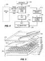
- FIG. 2is a block diagram of image processing and driving circuitry suitable for use in the tile shown in FIGS. 1A and 1B .
- FIG. 3is an exploded perspective drawing which illustrates a structure that may be used to implement the tile shown in FIGS. 1A and 1B .
- FIG. 4is an exploded perspective drawing which illustrates the electrical connecting structure of the tile structure shown in FIG. 3 .
- FIG. 5is an exploded perspective drawing which illustrates an alternative structure that may be used to implement the tile shown in FIGS. 1A and 1B .
- FIG. 6is a back plan view of a tile having the structure shown in FIG. 5 .
- FIG. 6Ais a pixel diagram which shows an exemplary pixel layout for portions of four tiles having the structure shown in FIG. 5 .
- FIG. 7is a pixel diagram which shows an exemplary pixel layout for portions of four tiles having the structure shown in FIG. 3 .
- FIG. 8Ais a front-plan view of a single color pixel structure which includes separate sub-pixels.
- FIG. 8Bis a front-plan view of an alternative single color pixel structure which includes separate sub-pixels.
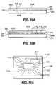
- FIG. 9is a front plan view of a tile having the structure shown in FIG. 3 which illustrates an exemplary method by which electrical connections may be made to the row and column electrodes of the tile.
- FIG. 10Ais a cut-away view of the tile shown in FIG. 9 along the line F 10 A which illustrates an exemplary contact structure for a column electrode.
- FIG. 10Bis a cut-away view of the tile shown in FIG. 9 along the line F 10 B which illustrates an exemplary contact structure for a row electrode.
- FIG. 11Ais a back plan view which illustrates an electrical connection structure suitable for use with a tile having the structure shown in FIG. 3 and the distribution structure shown in FIG. 8 .
- FIG. 11Bis a back plan view which illustrates a combined optical and electrical connection structure suitable for use with a tile having the structure shown in FIG. 3 .
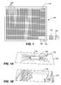
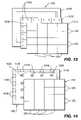
- FIG. 12is a back plan view of the tiled display shown in FIG. 1 which illustrates a power and signal distribution structure suitable for use with the tiled display.
- FIG. 13is an exploded isometric drawing which illustrates a first mounting method suitable for use with the tiled display shown in FIG. 1 .
- FIG. 14is an exploded isometric drawing which illustrates a second mounting method suitable for use with the tiled display shown in FIG. 1 .
- FIG. 15is a cut-away side plan view of a portion of the tiled display shown in FIG. 1 which illustrates an exemplary method for joining adjacent tiles.
- FIG. 16is a perspective view of a mullion suitable for use with the joining method shown in FIG. 15 .
- FIG. 17is a cut-away side plan view of the glass plate of a pixel of a tile having the structure shown in FIG. 3 or FIG. 4 which is useful for describing a method for forming a black matrix for the tile.
- FIG. 18is a cut-away side plan view of a portion of the glass plates of two adjacent tiles which shows how the tiles may be joined by a mullion such as that shown in FIG. 16 .
- FIG. 19is a cut-away side plan view of the glass plate of two adjacent pixels of a tile having the structure shown in FIG. 3 or FIG. 4 which is useful for describing a method for forming a black matrix for the tile.
- FIG. 20is a cut-away side plan view of a cathodoluminescent tile suitable for use in a tiled display according to the subject invention.
- FIG. 21is a schematic view of a first exemplary cathodoluminescent structure suitable for use with the tile shown in FIG. 20 .
- FIG. 22is a schematic view of a second exemplary cathodoluminescent structure suitable for use with the tile shown in FIG. 20 .
- FIG. 23is a front-plan view of the cathodoluminescent tile shown in FIG. 20 .
- FIG. 24is a schematic view of a third exemplary cathodoluminescent structure.
- FIG. 25is a schematic view of a fourth exemplary cathodoluminescent structure.
- FIG. 26is an isometric view of a cathodoluminescent tile suitable for use with the structures shown in FIGS. 24 and 25 .
- FIG. 27is a top-plan view of a cathodoluminescent tile such as that shown in FIG. 26 showing an optional electromagnetic deflection unit.
- FIG. 28is a cut-away view of a first deflection yoke suitable for use with the cathodoluminescent tile shown in FIG. 27 .
- FIG. 29is a cut-away view of a second deflection yoke suitable for use with the cathodoluminescent tile shown in FIG. 27 .
- FIG. 30is a front plan view of the cathodoluminescent tiles shown in FIGS. 24 through 29 .
- OLEDoptical light emitting diode
- LEDlight emitting diode
- BRCReflective Cholesteric
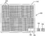
- FIG. 1is a front plan view of a partially assembled large-area display 100 according to the present invention.
- the display 100is a tiled display in which emissive or reflective elements, on which the image pixels are formed, are built as relatively small arrays on tiles 120 and assembled into a frame to produce the large-area display having a large number of pixel forming elements.
- the tilesmay be assembled side-to-side with their pixels aligned in rows and columns without a frame.
- the individual tilesmay be held together by mullions.
- the tilesare constructed with pixel forming elements evenly spaced up to the edges of the tiles. As described below with reference to FIGS. 15 through 19 , the tiles are formed such that, when they are joined, the inter-pixel distance between the edge pixels of two adjacent tiles is the same as the inter-pixel distance of adjacent pixels in the interior of a tile.
- the display shown in FIG. 1is missing two tiles 122 and 124 . These tiles are inserted into the positions 102 and 104 to complete the display.
- each tilemay include many more pixels.
- each tileincludes 896 pixel forming elements arranged as a 32 by 28 matrix. These tile sizes are only exemplary. It is contemplated that each tile may include more or fewer pixel forming elements.
- a single displaymay be, formed from tiles having differing numbers of pixel forming elements. For example, a display may have tiles with relatively large numbers of pixel forming elements near the center and tiles having relatively small numbers of pixel forming elements near the edges.
- FIGS. 1A and 1Bare perspective drawings showing the back and front surfaces of an exemplary tile 120 .
- the tileincludes a circuit board 130 on which is mounted at least one integrated circuit 134 .
- the integrated circuitis connected to the pixel forming elements through conductive traces 132 on the circuit board which are coupled to vias (not shown) that extend through the circuit board to make contact with the row or column electrodes of the display device.
- viasextend through the pixel forming elements internal to the display area, as described below with reference to FIGS. 9 , 10 A and 10 B.
- the viasmay extend through pixel forming elements along two edges of the display, as described below with reference to FIGS. 5 through 6A .
- the pixel forming elementsare made from an organic light emitting diode (OLED) material.
- the basic light emitting structureconsists of a thin organic polymer layer sandwiched between a pair of appropriately selected and patterned electrodes. Current flowing from one electrode to the other electrode causes the organic polymer to emit light. At least one of the electrodes is desirably transparent to the emitted light.
- Indium tin-oxideis the usual material used for this purpose. OLED materials provide high brightness and high efficiency, and are relatively low cost materials.
- An exemplary display structure according to the present inventionis formed in two parts: a display section and an electronics section. These two parts are made separately and then joined to form a complete tile.
- the display sectionconsists of a transparent glass layer on which are transparent column electrodes are deposited.
- the OLED materialis deposited onto these layers, as the active (i.e., light emitting) medium. Row electrodes are deposited as the final display layer. Additional layers such as blocking or passivation layers may be present to improve the function or life of the display layers.
- the transparent electrodeis preferably the hole injecting electrode and the other electrode is preferably the electron injecting electrode.
- the OLED materials between the electrodesare preferably conjugated polymer materials that are applied by thick film processes, however, small molecule materials can alternatively be applied by various thin film deposition techniques.
- the layersare patterned so that there is electrical access to each row and column at one or more points.
- the pixel forming elements of the tilesmay be any of a number of emissive devices such as electroluminescent elements, light emitting diodes, field emissive elements, plasma elements or cathodoluminescent elements.
- emissive devicessuch as electroluminescent elements, light emitting diodes, field emissive elements, plasma elements or cathodoluminescent elements.
- the electronics sectionis formed by punching or drilling vias through the circuit board and then printing or otherwise depositing the conductive traces on the circuit board.
- the conductive ink or paste used to form the conductive tracesmay also fill the vias.
- the viasmake contact with the row and column electrodes of the display section when the electronics section and the display section are joined to form a tile.
- another exemplary embodiment of the present inventionincludes a pixel forming structure that is appropriate for applications in which either a reflective or low power display is needed.
- the substrate and the electronics of this new structureare essentially the same as described below for the OLED embodiments.
- the display layer in this alternative embodimentis a reflective display material.
- a Bistable, Reflective Cholesteric (BRC) liquid crystal materialwhich provides for a low power, bistable display.
- BRCBistable, Reflective Cholesteric
- the disclosed tile structureenables, for the first time, video-rate displays in large area BRC displays. These materials switch between a planar, reflective state and a relatively transparent focal conic state. Utilizing a black backing, these two states may appear colored and black.
- the BRC materialsoffer distinct advantages for large area tiled displays: the operation between a reflecting and transparent state, combined with a black back-plane makes possible bright, high contrast displays under a variety of lighting conditions; and the bistability also allows for maintaining static images with no power applied.
- One exemplary tile structureconsists of a multilayer ceramic circuit board 132 that serves as a substrate upon which: the display material is mounted on the viewer side while the electronics 134 (active and passive) for drive or other functions are mounted mostly on the back side.
- Conductor elements 132are printed on the individual layers to provide interconnections between the electronics and the display material, vias interconnect the conductors in different layers; and connectors are provided on the back surface to connect to external power and signal sources.
- the tile structuremay also have a structural layer(s) such as a high softening point metal or insulator to provide freedom from distortion during the processing of the ceramic materials, and/or thermal management during the operation of the display.
- the tile structurealso contains a transparent layer (e.g. float glass) on the viewer surface to protect or contain the display material.
- a back panel structureis provided to mount the individual tiles and to provide electrical connection to the power and drive signals needed by each individual tile structure.
- the Multilayer ceramic circuit board 130may be formed of layers of ceramic material.
- the layersare first formed and processed to form vias, conductors, and other features and then assembled in a stack taking care to carefully align each layer with those layers adjacent to it.
- Ceramic materialhere is meant in the broadest sense to include ceramics, glass ceramics, glass, and other high temperature insulating materials.
- the multiple layers together with the connectors and viasprovide the basic function of a circuit board upon which active and passive electrical devices and circuits can be placed.
- the conductors 132may be thin and/or thick film conductors formed by any of the standard processes including, for example plating, evaporation, sputtering, printing and laminating.
- the materialsmay be metals or organic conductors.
- the conductorsmay be patterned by processes that may include, for example, printing or photolithography. These conductor patterns are formed on the surfaces of the individual layers in the disclosed structure and connect to the vias to provide, according to the design of the device a means of interconnecting the electronics on and external to the disclosed structure to the display material.
- Viais used in the broadest sense and includes conductors that go through openings in the layer and those that go around the edge of a layer(s). Vias that go through a layer can be formed, for example, by making a hole in the layer and filling that hole with a conductor. Alternatively, pre-formed physical conductors may be imbedded in the layer. Vias that go over the edge of a layer(s) can be formed by physically placing a wire (round or flat), or array of wires, and wire bonding the ends to the surfaces to be interconnected. Alternatively they can be formed in place by plating or other fabrication process for thick or thin film conductors.
- a core layermay also be included in this structure.
- This layertypically has a higher softening point than the ceramic materials and serves as a substrate for the assembly and processing of the ceramic material.
- the core layeracts to: eliminate horizontal shrinkage; establish a single coefficient of expansion for the multilayer system, and provide mechanical ruggedness to the multilayer assembly. If the layer is a good electrical conductor it may also provide RF shielding. If the layer is also a good thermal conductor, it contributes to the thermal management of the display. Conductive layers, however, present a special problem for via connections.
- Via connections through metal layerscan be fabricated in several ways: filling the periphery of the hole with an insulating material before putting a metal conductor through the middle, or by putting the conductor only through the middle leaving space separating the conductor from the conductive metal core.
- the electronics which form the image processing and pixel driving circuitryare mounted on the layers. Electronics are used in the broadest sense to include both active and passive, and both discrete devices mounted on the layers and devices formed in place by processes such as those now used to make active matrix circuits for displays on various high temperature substrates. While these electronics can be placed anywhere, the most convenient location is the back surface. This permits standard assembly and attachment equipment and processes to be used. In addition, the placing of active or passive devices on the intervening layers or viewer surface permits greater flexibility in the system design.
- the display materialis applied to the surface visible to the viewer. Because of the flexibility of the construction of the disclosed structure, different display materials can be used.
- edges of the tilesare desirably carefully formed to ensure that the tiled display has no visible seams between the tiles.
- One criterion for the tilesis that the spacing between the pixels separated by the tile seam is the same as the spacing of pixels on the tile.
- the tile edgesare desirably dimensionally precise.
- the edgesare also used for conductors or if mullions are used to join adjacent tiles, it is desirable to account for the thickness of these conductors or mullions in the design and placement of the tiles.
- a backpanelmay be provided for the physical mounting and interconnection of the tiles to form a display.
- the mounting of the tilesis done such that there is a continuity in the pixel spacing over the display.
- the shape of the tilesis most typically square or rectangular, however the shape can be any shape that can be tiled to form a larger display.
- the tileis typically flat, but may be curved along one or both dimensions to form curved or domed displays. Curved or domed displays can also be made using flat tiles mounted on a curved or domed backpanel.
- Tilesmay be attached to the backpanel either by permanent connection such as soldering or using connectors which allow the tiles to be plugged into the backpanel. This latter method permits the repair and replacement of individual tiles.
- Different types of tilesmay be attached to different areas of the backpanel—for example, higher resolution areas may be placed in the center or other areas of the large display.
- different sized or different shaped tilesmay be combined in a single display. For example, tiles near the edges of a large panel may be larger and have a lesser pixel density than tiles near the center of the panel.
- the back panelmay also provide the means for connecting the tiles to the operational power and data signals needed to operate the tile.
- Matching connectorsmay be provided on both the backside of the tile and the backpanel to provide this connection.
- optical connectionmay be used as an alternative to physical connection.
- tiled displayOne advantage of the tiled display is that the scan electronics can be internal to the tile and the scan rate of any one tile is the same for a small display or for a large display. This ensures that the brightness and gray scale of the display do not degrade with increasing size.
- the tiled displays described in detail belowhave an architecture which connects the signals to the pixels without interrupting the continuity of the pixel spacing, even at the edges of the tiles.
- the disclosed tiled displaysmay also have signal processing circuitry which extracts the signal information for that tile from a broadcast information signal and transforms the extracted information into the signals needed to address that tile.
- the front-to-back connectionsinclude one for each row of pixels and one for each column of pixels on the tile.
- Tiled displayshave relatively few pixels so that the number of interconnects per tile is relatively small and the yield on individual tiles can be high. This is a significant advantage of tiled displays when compared to fabrication of large displays from single substrates. In general, the yield is a function of the number of pixels in the display device.
- the final connection to the row or columnis made with a via that extends from the back surface of the tile.
- This viahas a diameter less than the spacing of a pixel.
- the portions of the vias in the display layer(s)may be made smaller than the vias through the other intervening layers, and, as described below, the connections may be staggered over the area of the tile to provide maximum spacing between the wider interconnects. These connections are the final link in the distribution of the display signals to the pixels.
- FIG. 2is a block diagram of electronic circuitry which is suitable for use with a display tile according to the present invention.
- the operational power connectionse.g. power and ground
- FIG. 2is a block diagram of electronic circuitry which is suitable for use with a display tile according to the present invention.
- the operational power connectionse.g. power and ground
- a field programmable gate array (FPGA) 210which comprises the timing and sequence logic receives a timing and control signal and a data signal. As described below, these signals may be provided to the tile by an electrical wiring harness or through an optional optical interface 224 (shown in phantom).
- the timing and control signalincludes a system clock signal, a synchronization signal and control values which may change the functions performed by the display electronics.
- the timing and sequence logic circuitry 210may provide a clock signal, CLOCK, to the optical interface 224 .
- the circuitry shown in FIG. 2may be viewed as having four functions: loading and storing compensation data for an individual tile, loading and storing display data for the tile, displaying the stored data, and adjusting to compensate for changes in the brightness performance of individual pixels.
- the level of light emitted by a particular OLED pixelis a function of the level of current provided to that pixel.
- the brightness of each pixel in the displayis controlled by controlling the magnitude of current that is supplied to that pixel during normal operation.
- each pixelis either turned on or off. Gray scale is achieved by changing the relative amount of time that one pixel is turned on.
- the amount of light emitted by a pixel when it is turned onis controlled by controlling the level of current applied to the pixel in the on state.
- the level of current applied to each pixelmay be adjusted to match the amount of light emitted by the pixel to the amounts of light emitted by every other pixel in the display device.
- the pulse width of the pulse which drives the pixelis changed to modulate the brightness of the pixel when an image is being displayed on the tile.
- the exemplary embodiment of the inventionemploys a passive addressing technique within a block in which only one row of pixels is illuminated at any time.
- the scanning circuitrysteps through each row on the tile and illuminates that row for a predetermined interval. Because each tile is individually scanned, all of the tiles may illuminate a row simultaneously. Thus, each time a single tile refreshes its pixels, the entire display device also refreshes its pixels.
- the row selection circuitry 222may be, for example, a conventional clocked shift register having a number of stages equal to the number of rows in the addressing block.
- the shift registerclocks a single logic-high value through the rows of the addressing block. As the logic-high value is applied to each row, the pixels in that row are selected.
- the current applied to a pixel cell on the display deviceis controlled responsive to a value for the pixel cell that is stored in the non-volatile memory 214 .
- the addresses of the pixels on the lineare applied to the memory 214 , which provides a number of compensation values to the programmable current sources 216 .
- the number of values providedequals the number of columns in the display device.
- Each valueis applied to a respectively different programmable current source to provide respective current values to the pixels in the selected row.
- the programmable current sourcesare coupled to the column drivers 220 . When the column drivers are enabled, they each provide a level of current determined by a respective one of the programmable current sources 216 .
- the display of pixel datais controlled by pulse-width modulating the current signals provided to the selected row of pixels.
- a random access memory 212stores a number of pixel values which may, for example, correspond to the number of pixels on the tile.
- the timing and sequence logic 210selects a row, fetches the line of data corresponding to the selected row and applies the selected data to the pulse width modulator (PWM) 218 .
- the PWM 218converts the binary values into respective pulse widths and controls the column drivers to apply the current levels provided by the programmable current sources 216 to the column electrodes of the tile.
- the memory 212may hold more or less data than would be required to operate the number of pixels on the tile. If the memory holds less data, then new data may need to be stored into the tile while previously stored data is being displayed. If the memory 212 holds more data, then the circuitry shown in FIG. 2 may display image data for a row of pixels from one image frame while a row of data from the next image frame is being loaded into the memory 212 . In general, it is contemplated that the various functions performed by the electronic circuitry shown in FIG. 2 , loading compensation data, loading pixel data and displaying pixel data may be performed concurrently.
- the timing and sequence logic 210receives the timing and control signal and decodes the control signal to determine which functions are to be performed.
- each tilemay be calibrated to a nominal brightness value by, for example, mounting the completed tile onto a test fixture which has a photocell corresponding to each pixel position.
- Each pixelis individually turned on and its brightness is compared to the nominal brightness and a control value for the pixel is applied to the programmable current source 216 for that pixel.
- the value applied to the current source 216is stored into the non-volatile memory 214 .
- the tilemay also include circuitry which automatically adjusts the pixel brightness to compensate for aging of the display material.
- This circuitrymay, for example, allow a viewer to display a predetermined brightness value, select an individual tile and adjust the brightness value up or down to match the brightness of the selected tile to match its neighbors.
- the tilemay include a small light sensor over one or more pixel positions which continually monitors the brightness of that pixel and adjusts the current level applied to that pixel—and the current levels applied to all of the other pixels on the display—to compensate for variations in pixel brightness due to aging of the display. To minimize the visibility of the light sensor, it may be placed away from the active pixel area so that it is responsive to scattered light.
- the circuitry 134may include an all electronic compensation system which continually adjusts the brightness of individual pixels to compensate for aging.
- the inventorhave determined that the decay in the brightness of an OLED pixel that occurs with aging can be predicted by measuring the current and time for a particular pixel, and integrating the product of current and time. This product can be fitted to a characteristic curve and used to adjust the drive current to predict a new drive current which restores the original brightness level of the pixel.
- the rate of decay for different pixelsdiffers slightly, and the initial decay slope can be measured during burn in and used as a second order correction factor in the algorithm for calculating any change in drive current for that pixel.
- the exact form of this adjustmentdepends on the geometry of the pixels and the materials that are used to form the pixels. A suitable adjustment may be readily determined by one skilled in the art of designing OLED displays by monitoring the performance of an exemplary pixel over time.
- This algorithmcan be incorporated in the electronics on the electronic drive block, and the result is that the brightness can be maintained at constant brightness automatically without manual adjustments.
- This proportionality constantvaries for different pixel geometries and different OLED materials. It can be easily determined by one skilled in the art of designing OLED displays by monitoring the performance of an exemplary pixel over time.
- an external system of reestablishing the brightness uniformitymay be employed.
- a systemmay, for example, incorporate a sensor that detects and measures individual pixel brightness and some means to communicate with the display electronics so that the correct drive voltage needed to establish the desired brightness can be stored in the display tile memory.
- any of these methods for adjusting the current applied to a pixel in order to maintain a predetermined brightness levelmay be combined with any other method either as a check or to augment the performance of the other method.
- the exemplary display devicecalibrates the brightness of the pixels using a method (i.e. current control) which is orthogonal to the method (i.e. pulse-width modulation) which is used to control the pixels to achieve gray scale.
- a methodi.e. current control
- the methodi.e. pulse-width modulation
- FIG. 3is an exploded perspective diagram which shows a first exemplary tile structure.
- the tile structureis formed in two parts: the display section and the electronics section.
- the display sectionincludes a transparent front plate which may be, for example, a float glass plate.
- Transparent column electrodes 322are formed on the front plate 320 by forming thin bands of a transparent conductor, such as indium-tin oxide, using well known processes. This may be done, for example, by depositing a film of ITO over the surface of the float glass plate and selectively etching the ITO to form the electrodes.
- the display materials, red, green and blue OLED materials 324 and 326including a hole transport layer, a light emitting layer and an electron injecting layer, are deposited on top of the column electrodes to define the active area of the pixel.
- the hole transport layeris electrically coupled to the column electrodes, and the light emitting layer is electrically coupled to the hole transport layer.
- the electron injecting layerwhich may, for example, be formed from metallic calcium is formed on top of the light emitting layer.
- the row electrodes 328are formed on top of the electron injecting layer. As described below with reference to FIGS. 6A and 7 , it is desirable for the display materials 324 and 326 to occupy only a portion (e.g. about 25 percent) of the pixel area.
- the row electrodesmay be formed, for example, from polysilicon or from a metal such as aluminum using standard deposition techniques.
- An insulating layer 330is formed on top of the row electrodes.
- the exemplary insulating layer 330may be formed from any of a number of insulating materials. To protect the display materials, the insulating layer 330 is desirably formed using low-temperature processes. Exemplary materials include Polyimide or other low-temperature inorganic materials. The insulating layer 330 may be applied using thick film or thin film deposition techniques. The insulating layer 330 includes a plurality of openings 331 aligned with the row electrodes 328 or column electrodes 322 .
- the plates 332may be formed using, for example, vapor deposited aluminum or a metallic ink or paste, such as silver combined with a solvent, which is deposited using thick film processes.
- the connecting platesare coupled to the column electrodes 322 and row electrodes 328 by vias which extend through the openings in the insulating materials.
- Each of the exemplary connecting platesmakes electrical contact with only one row electrode or one column electrode. To ensure that a good connection is made, however, each connecting plate 332 may connect to its corresponding row or column electrode at several locations.
- the electronics section 312includes image processing and display driving circuitry 134 (not shown in FIG. 3 ) a circuit board 130 , which may be, for example, a thin sheet of alumina (Al 2 O 3 ), deposited electrical conductors 132 , connecting pads 334 and vias 338 which electrically connect the conductors 132 to the connecting pads 334 through the circuit board 130 .
- the conductors 132 , vias 338 and connecting pads 334may all be formed using thick film deposition processes to apply a metallic ink or paste.
- the connecting pads 334may also be formed from vapor-deposited aluminum. There is a one-to-one relationship between the connecting pads 334 of the electronics section and the connecting plates 322 of the display section. In the exemplary embodiment of the invention, the connecting pads 334 and the connecting plates 322 are electrically connected by applying an anisotropically conductive adhesive between the display section and the electronics section.
- the combined display section and electronics sectionforms a tile 120 .
- the connecting plates 322 and connecting pads 334may be made from a deformable material and patterned to include a portion which extends above the plane of the pad or plate.
- the patterned material on the connecting plates 322 and connecting pads 334comes into contact and deforms, forming an electrical connection between the corresponding connecting pads and plates.
- the pads 334 and plates 322may also be connected by bump-bonding techniques or using wires that are implanted in one of the pads 334 or plates 322 and engage the plate 322 or pad 334 when the electronics section 312 is mated to its corresponding display section 310 .
- FIG. 4is an exploded perspective drawing of a portion of the electronics section 312 . This drawing more clearly shows the electrical connecting structures of the electronics section.
- the circuit board 130includes a plurality of openings 410 each of which corresponds to a respective connecting pad 334 .
- the vias 338are formed in the openings 410 at the same time that the connecting pads 334 are formed on the front surface 412 of the circuit board.
- the electrical conductors 132are formed on the back surface 414 of the circuit board 130 to connect the image processing and display driving circuitry 134 (not shown in FIG. 4 ) to the various connecting pads 334 .
- FIG. 5is an exploded perspective drawing which illustrates an alternative structure of an exemplary tile 120 .
- the tile shown in FIG. 5may be formed as a separate electronics section and display section or it may be formed as a single structure.
- the connections to the row and column electrodes of the tileare made along two edges of the tile.
- the circuit board for the tile shown in FIG. 5is the bottom layer 510 .
- This circuit boardmay include, for example, an electronics module such as the circuit 134 shown in FIG. 1A .
- the electronics moduleis coupled to the row and column electrodes of the display device through column vias 520 and row vias 522 . Only one row via 522 is shown in FIG. 5 .
- the circuit boardis level 510 and optional levels 512 , 514 and 516 , shown in phantom, are interconnecting layers. These may be ceramic layers having vias to connect to higher layers and conductive traces painted or printed on one surface of the layer.
- one of the layers 512 or 514may be a metal or insulating structural substrate.
- Layer 516is a ceramic layer having column vias 520 and row vias 522 . The row vias formed on the ceramic layer 516 connect to the row electrodes 524 of the exemplary display tile.
- the electronics sectionincludes only the layer 510 and the optional layers 512 , 514 and 516 . If the tile is formed as a single piece then the display material 526 is deposited on top of the row electrodes 524 . In the drawing FIG. 5 , the display material 526 is illustrated as a solid sheet. This material, however, may be individual electron injecting layers and individual OLED cells deposited on the row electrodes. As described above with reference to FIG. 3 , the row electrodes may be formed from a metal such as aluminum or from polysilicon.
- the column electrodes 528are formed on top of the display material 526 .
- the column electrodesare connected to the circuit board through the vias 520 which extend through each level of the display tile from level 510 through level 526 .
- Each column electrodeis coupled to a respectively different via 520 .
- the column electrodes 528are typically formed from a transparent conductive material such as indium-tin oxide (ITO).
- ITOindium-tin oxide
- level 530formed above the column electrodes 528 may be an optical filter or it may be a patterned black matrix which covers the inactive areas of the display layer 526 with black lines while providing openings for the active elements of the display material.
- the final layer of the display tile shown in FIG. 5is a float glass front cover 532 .
- the display sectionmay be formed, as described above with reference to FIG. 3 .
- the filter or black matrix layer 530is deposited on the float glass cover 532 .
- the transparent column electrodes 528are deposited, then the OLED materials are formed on the column electrodes and the row electrodes 522 are formed to cover the OLED materials.
- the exemplary separate electronics and display sections shown in FIG. 5may be joined by bump-bonding the row and column vias along their edges or by inserting conductive elements, for example wires, into the row and column vias on one of the sections such that the conductive elements protrude from the vias. The conductive elements would then mate with the corresponding vias on the other section when the sections are joined.
- the tile structure shown in FIG. 5may be formed by first preparing green tape blanks for the layers 510 , 512 , 514 and 516 . Next, the blanks are punched with holes through which the vias 520 and 522 will be formed. After the blanks are punched, they may be painted or printed with suitable conductive material to fill in the vias and to provide any conductive traces which may be needed to interconnect other circuitry in the display tile.
- the traces printed on the green tape sheet 516may include the row electrodes 524 .
- This structure including layers 510 , 512 , 514 and 516 as well as the vias 520 and 522 and the row electrodes 524is then laminated and fired to form a ceramic substrate for the circuit component of the display device.
- the display materials 526are deposited on the row electrodes 524 . After depositing the display material 526 , the column electrodes are formed on the tile using conventional processes for depositing ITO.
- the black matrix or filter 530may be formed on the float glass cover 532 .
- the combined mask and coveris then aligned with the display device such that the openings in the mask correspond to the active pixel regions of the display material.
- the glass cover 532is then sealed to the composite fired ceramic structure using, for example, a frit glass.
- FIG. 6is a bottom plan view of the display tile shown in FIG. 5 .
- the circuit board 510includes electronic circuitry 134 ′ which is connected to the rows and columns of the display through the vias 520 and 522 respectively.
- the conductors 602 which connect the circuitry 134 ′ to the vias 520 and 522may be printed or painted onto the green tape prior to firing, as described above.
- the connectors 602are coupled to the vias 520 and 522 along the edge of the circuitry 134 ′.
- the circuitry 134 ′is coupled to receive operational power via conductors 610 and to receive the data signal and timing information via conductors 612 and a connector 614 .
- the connector 614may be coupled to a cable harness when the tile 120 ′ is assembled into a tiled display device such as the device 100 shown in FIG. 1 .
- FIG. 6Ais a pixel diagram which illustrates an exemplary pixel spacing that may be used in the tile shown in FIG. 5 .
- This pixel spacingallows the conductive vias to be arranged along the edge of the tile, without locally distorting the inter-pixel distance in the assembled tiled display.
- FIG. 6Aillustrates portions of 4 tiles, 630 , 640 , 650 , and 660 .
- the dashed lines 624 and 622illustrate pixel boundaries. These lines are provided only as a guide in understanding the pixel layout.
- the active portion 526 of the pixelsoccupies only about 1 ⁇ 4 of the total pixel area. This defines a pixel aperture of approximately 25%. In this exemplary embodiment of the invention, the active region is not centered in the pixel area but is offset to the left and top as shown in FIG. 6A .
- this spacing of the pixelsleaves room along the edges of the display for the vias 520 and 522 to connect to the row and column electrodes of the pixel without interfering with the regular spacing of the pixels across tile boundaries.
- the distance d ewhich is the distance from the active region 526 to the edge of the tile, is approximately twice the distance d I which is the internal distance from the edge of the active area of the pixel 526 to the pixel boundary 522 or 524 .
- the active region of the pixelmay be offset both horizontally and vertically, it is contemplated that the active area may be offset only vertically. In this configuration, the contacts to the row electrodes are beneath the active pixel material and, thus, do not need to offset the active region of the pixel.
- FIG. 7is an alternative pixel layout, suitable for use for a tile such as that shown in FIG. 3 .
- the active portions 526 of the pixelsare centered in their respective pixel regions and the vias which connect the row and column electrodes of the display to the electronics are formed between respective pixel elements.
- the distance between the edge of an active region 526 and the edge 712 of the displayis equal on all sides of the tile and the distance from the center of the active pixel region to the edge is 1 ⁇ 2 of the pixel pitch.
- the distance between the center of an edge pixel and the edge of the tilemay be slightly less than 1 ⁇ 2 of the pixel pitch in order to allow a mullion to be inserted between adjacent tiles.
- mullionsare typically used both to join tiles on the display device and to hide the edges where the tiles meet.
- FIGS. 8A and 8Bshow a single pixel having separate red (R) 820 , green (G) 822 and blue (B) 824 sub-pixels.
- the three sub-pixels 820 , 822 and 824each have a respective column electrode (not shown) which is connected to the electronics section by the vias 810 , 812 and 814 , respectively.
- a single row electrode (not shown)is used by all three of the sub pixels. This row electrode is coupled to the electronics section by the via 816 , shown in phantom.
- the geometry of the triple sub-pixel structureis defined by d SH , the height of the sub-pixel, d SW , the width of the sub-pixel, and d e , the distance from the active sub-pixel areas to the edge of the pixel area.
- these dimensionsare given in Table 1 in terms of the pixel pitch, P.
- FIG. 8Billustrates an alternative color pixel structure.
- This structureincludes four sub-pixel elements, 830 , 832 , 834 and 836 . Two of these sub-pixel elements, 830 and 836 emit green light when stimulated while the other two pixel elements, 832 and 834 emit red and blue light, respectively.
- This structureis known as a quad sub-pixel structure. The structure uses two green sub-pixels because more of the luminance information in a color display is in the green pixels than is in either of the red or blue pixels. Thus, the use of two green sub-pixels allows for a brighter display.
- the pixels 830 and 836may both be red or blue pixels.
- the amount of light emitted by the red or blue pixel materialmay be less than the amount of light emitted by the green pixels.
- making the pixels 830 and 836 both be red or blue pixelswould improve the overall brightness of the display.
- the pixel structure shown in FIG. 8Bemploys two row electrodes (not shown) and two column electrodes (not shown). The row electrodes are coupled to the electronics section by the vias 816 ′ and 818 (shown in phantom) while the column electrodes are coupled to the electronics section by the vias 810 ′ and 812 ′.
- the geometry of the quad sub-pixel structureis defined by the dimensions d SH , the height of the sub-pixel, d SW , the width of the sub-pixel, d e , the distance from the active sub-pixel areas to the edge of the pixel area, and d SI the distance between adjacent sub-pixels. These values are defined in Table 2 for the exemplary embodiment of the invention.
- FIGS. 8A and 8Bshow the distances d e and d SI as being equal in the horizontal and vertical directions, it is contemplated that these values may be different.
- the exemplary pixel structures shown in FIGS. 8A and 8Bboth have active pixel areas covering approximately 25 percent of the pixel area to produce a pixel aperture of approximately 25 percent. This value is exemplary only. The invention contemplates both larger and smaller pixel apertures.
- FIG. 9is a front plan view of an exemplary tile with the connecting plates 332 shown as dashed line boxes. The insulating layer 330 has been removed for clarity.
- FIG. 9also includes two row electrodes 328 A and 328 B and two column electrodes 322 A and 322 B. Column electrode 322 A is shown as being connected to connecting plate 332 A through the vias 914 . Column electrode 322 B is shown as being connected to connecting plate 322 D through the vias 916 . Row electrodes 328 A and 328 B are coupled to the respective connecting plates 332 B and 332 C through the vias 910 and 912 respectively.
- FIGS. 10A and 10Bshow cutaway views of a portion of the electronic section shown in FIG. 9 along the lines F 10 A and F 10 B respectively.
- FIGS. 10A and 10Binclude the insulating layer 330 which was omitted from FIG. 9 .
- the connections 916 to the column electrodes 322 Bare made on a region of the display tile which is between active pixel elements.
- FIG. 10Ashows only the float glass substrate 320 , the column electrodes 322 , the insulating layer 330 , and the connecting plates 332 D and 332 E.
- the via 916 between the connecting plate 332 D and column electrode 322 Bis made through the opening 331 in the insulating layer 330 .
- This connectionmay be made for example, when the connecting plate is printed on the electronics section by allowing the silver paste or ink used in the printing process to flow through the opening 331 and make contact with the column electrode 322 B.
- FIG. 10Billustrates an exemplary method for making connections to the row electrodes.
- the connections to the row electrodesare made on a portion of the display containing the active pixel elements 324 .
- the segment of the display shown in FIG. 10Bincludes the glass substrate 320 , transparent column electrodes 322 display material 324 and row electrode 328 B.
- the connecting plate 332 Bmakes connection with the row electrode 328 B using the vias 910 . This connection is made through the openings 331 in the insulator 330 .
- there are several openingssuch that connection between the connecting plate 332 B and row electrode 328 B may be made at several locations.
- FIG. 10Bshows the connection between the connecting plate 332 B and row electrode 328 B being made in the space between respective pixels 324 , it is contemplated that these connections may be made anywhere along the row electrode 328 B and need not be limited to spaces between active pixel elements.
- connections to the column electrodesare also made at a plurality of locations along the connecting plates. Referring to FIG. 9 , for example, there are three vias 916 representing connections between the connecting plate and 332 D and the column electrode 322 B.
- each connecting platemakes electrical contact with only one row electrode or column electrode, it is desirable for the number of connecting plates implemented in a display tile to be greater than or equal to the sum of the number of columns and the number of rows in the tile.
- each connecting platemay cover 12 pixel positions arranged in a 2 by 6 matrix. Because the locations at which connections may be made to the column electrodes are more limited than the locations at which connections may be made to the row electrodes, the exemplary connecting plate may cover 2 row pixel positions by 6 column pixel positions.
- ITOis not as good a conductor as aluminum or silver
- the number of connecting plates 332 and connecting pads 334may be greater than the sum of the number of row electrodes and column electrodes.
- tile configurationsare contemplated by the subject invention.
- One desirable configurationis a tile which extends the full length (height) of the display and has a width of, for example, 32 columns.
- a tile having this shapewould require only horizontal (vertical) alignment.
- the connecting plates and connecting padsmay be made to cover many more columns than rows, providing many more locations at which to make connections to the column electrodes than if the connecting plates and connecting pads were approximately square.
- a displaymay be formed from different shaped tiles, for example long tiles that span the entire height of the display on the sides and smaller, square tiles near the center of the display.
- the different tilesmay also employ different pixel pitches such that the tiles on the sides of the display may have a relatively large pixel pitch while the tiles near the center of the display have a relatively small pixel pitch.
- the exemplary embodiments of the inventionshow the electronics sections of the tiles being the same size as the display sections, it is contemplated that these may be different sizes.
- a single electronics section(not shown) may be as large as two contiguous display sections (not shown). When assembled into a single tile, two display sections would be aligned with and bonded to the single electronics section.
- an electronics sectionis formed which spans the entire display device and individual display section tiles are mounted onto the electronics section.
- the electronics sectionmay include multiple electronics modules 132 .
- the electronics sectionsmay be smaller than the display sections.
- an entire displaymay consist of a single display section (not shown) that is bonded to multiple electronics sections (not shown). It may be desirable to manufacture the display sections and the electronics sections in different sizes to maximize yield of both components.
- the assembly of multiple display sections onto a single electronics sectionshould align the pixels such that no seam is visible between contiguous display sections.
- FIG. 12illustrates one way in which a plurality of tiles or a plurality of electronics modules on a single large tile may be connected to form a composite display device.
- FIG. 12shows the display device 100 from the back.
- the exemplary display deviceincludes a plurality of tiles 120 each of which includes an electronics module 134 .
- the electronics modulesare coupled to a central controller by a cable harness 1210 which includes a central cable and branching cables 1212 , 1214 , 1216 , 1218 , 1220 , 1222 , 1224 , and 1226 .
- each tileis coupled to four conductive lines, two of which convey operational power, one which conveys the data signal and one which conveys timing information.
- the operational power lines for the displaymay be shared among several tiles.
- the signal lines in this exemplary embodiment of this inventionare not shared. It is contemplated that, by including addressing circuitry in the electronics module 134 on each tile, the signal and timing lines for the entire display device may also be shared. In this configuration, each module recognizes and stores only the portion of the data in the address range of the tile.
- FIG. 11Ais a bottom plan view an exemplary type of tile 120 , such as that shown in FIG. 3 , which receives the data and timing signals electrically.
- the tile shown in FIG. 11Aincludes electronic circuitry 134 ′ and a plurality of conductive traces 1114 all mounted on a circuit board 312 .
- the operational power signal 612are received via the connector 1112 as are the data and timing signals 610 .
- the tiles shown in 11 Bmay be configured in a display in the same manner as the tiles described below with reference to FIG. 12 .
- the operational power signalmay be shared among all of the tiles while the timing and data signals are distributed to each tile individually.
- the timing and data signalsmay be shared by all of the tiles if each tile includes addressing circuitry to selectively separate its data from the data broadcast to all of the tiles.
- the multiplexing of data to the tilesmay be limited to a predetermined maximum. If the number of tiles exceeds this maximum value, only a portion of the display is updated at any given time.
- FIG. 11Bis a back plan view of a another type of tile 120 which receives its timing and data signals optically rather than electrically.
- the tileincludes an electronics module 134 and a plurality of conductive traces 1114 formed on a circuit board 312 .
- the electronics module 134 shown in FIG. 11Bis coupled to receive only operational power at the connector 1112 Data signals and timing information are conveyed to the module 134 via an optical coupling 1110 which is a part of the electronics module 134 .
- the exemplary optical coupling 1110may receive one or more optical fibers in a direct connection or may include a photosensitive area which receives a broadcast timing and data signal.
- the electronics module 134may include addressing circuitry to separate out the data which is addressed to the particular tile and store only that data for display.
- An optical interface suitable for use in the electronic circuit 134 in FIG. 11Bis describe in U.S. Pat. No. 5,281,805 entitled, OPTICAL-INPUT LATCH-CIRCUIT CELL ARRAY to Sauer, which is incorporated herein by reference for its teachings on optical interfaces.
- FIG. 13is an exploded front plan view of an exemplary tile assembly according to the present invention.
- the exemplary assembled display device 130includes a frame 1310 in which is mounted a rigid back panel 1312 .
- the back panelincludes connectors 1316 to provide operational power to each of a plurality of display tiles 120 and a pair of connectors 1318 (only one of which is shown in FIG. 13 ) which provide the data and timing information to each tile 120 of the assembled display device.
- the connectors 1316 and 1318may be solder-type connections or they may be plug-type connectors. Plug-type connectors may be preferred when easy access to the individual tiles is desired, for example, to enable defective tiles in the display to be replaced.
- the back plane 13may be assembled by mounting the individual tiles 120 on the back plane 1312 and then mounting the assembled back plane and tile display on to the frame 1310 .
- the assembled displaymay then be covered with a float-glass plate (not shown), which acts to protect the tiles and, optionally, may act, with the back plane 1312 and the frame 1310 to form a hermetic seal for the assembled display device 100 .
- a float-glass plate(not shown), which acts to protect the tiles and, optionally, may act, with the back plane 1312 and the frame 1310 to form a hermetic seal for the assembled display device 100 . Because the spacing between the tiles is desirably kept within close tolerances to maintain a substantially constant pixel spacing across the display, the tolerances for the connectors formed on the backs of the tiles 120 and on the back panel 1312 are desirably precise.
- a self aligning structuresuch as that shown in FIG. 14 may be used.
- This structuredoes not require the precise manufacturing tolerances of the structure shown in FIG. 13 .
- the frame 1410includes a plurality of spring elements 1418 .
- the power, timing, and data signalsare brought to the individual tiles by respective flexible connectors 1416 .
- the connectors 1416may also act to push the tile forward to make contact with a float-glass front plate (not shown).
- the connectors 1416are coupled to receive the power, data and timing signals via a wiring harness 1422 .
- each of the tilesis mounted, within the frame 1410 , on its respective flexible connector 1416 .
- the springs 1418 of the frame 1410tend to confine the tiles to an area indicated by the dashed line box 1420 .
- the springs 1418act to hold the tiles in alignment.
- the edges of each tilemay be formed in complementary patterns (not shown) such that the patterns of adjacent tiles mate, holding the tiles in alignment.
- opposite edges of a tilemay be patterned with complementary serrated edges which allow each tile to mate with an adjacent tile in only one position. It is contemplated that these edge patterns may be made on the display section or on the electronics section. Making the edge patterns only on the electronics section is desirable as it simplifies the edge fabrication for the display sections.
- the design shown in FIG. 14may be advantageous as it does not require precision assembly of the components as may be required by the design shown in FIG. 13 .
- FIGS. 15 through 19illustrate another exemplary method by which tiles 120 may be joined to form a composite tiled display 100 .
- a black matrixmay be fabricated from black lines.
- the black matrixis put between the active portions of the pixels to absorb ambient light in these areas in order to increase the display contrast.
- Black matrix linesmay be found, for example between the phosphors on the front screen of a CRT or between the pixel positions defined for a liquid crystal display.
- black matrix linesare typically smaller than mullions and are typically placed in the plane of the pixels. Because the black matrix lines are periodic and placed between the pixels, they do not tend to break the continuity of the image.
- FIG. 19is a cut-away drawing of a partially assembled display device.
- the main components of the structure shown in FIG. 19a transparent sheet 2020 of, for example, glass or plastic, a plurality of black lines 2010 that form a black matrix and the tiles 120 which form the display.
- the key feature of the optical integrator structureis a pattern of black lines 2010 which are like black matrix lines in that they have equal widths and a spacing equal to the pixel pitch.
- black lines 2010may be aligned to lie between all pixels in the display, including those pixels on either side of the gaps 2012 between the tiles 120 .
- the optical integrator pattern of black linesare also like mullions in that some of the black lines in the optical integrator structure lie on top of the gaps between the display tiles and block their visibility.
- the glass substrates 320 of the tiles 120are positioned adjacent to the black lines 2010 on the back surface of the transparent sheet 2020 , which forms the integrating structure.
- the disclosed optical structure for integrating display tilesis placed above the plane containing the pixels (like mullion structures), on the viewer-side of the tiles 120 , with the black line pattern being in contact with the display tiles.
- the black lines on the optical integrator structure 2020are relatively narrow, so that the black lines which cover the mullions are essentially the same width as the black lines which form the black matrix.
- the disclosed structuresimultaneously provides the functions of the black matrix and the mullions, but the mullion lines are not visible, as such, to the viewer because all lines in the pattern on the optical integrator structure 2020 are essentially the same and are virtually indistinguishable. Accordingly, the viewer simply sees a uniform pattern of black lines.
- a key feature of this aspect of the subject inventionis the precise specification of the pattern of black lines and mullions on the disclosed optical integrator structure so that the physical gaps between tiles are hidden from the viewer, and at the same time so that little or no emitted light is blocked from exiting the display.
- the black matrix and the mullionsdo not disturb the continuity of the larger image, even across the gaps between tiles.
- FIG. 15is a cross section of portions of two tiles 120 , according to the present invention, which are joined by a mullion.
- Each of the tilesincludes a glass substrate 320 and the remainder of the tile structure 1510 .
- the exemplary tilesinclude active display material 1514 located proximate to the bottom surface of the glass substrate 320 .
- the exemplary tilesalso include a mullion 1512 and black lines 1513 which form a portion of the black matrix.
- FIG. 16is a perspective drawing of an exemplary mullion 1512 suitable for use with a display device according to the subject invention.
- the mullion 1512includes a top surface 1610 which may be formed from a black material or may be printed or painted black. To ensure that the mullion does not create artifacts on the display device, it is desirable for the top surface of the mullion to closely match the black stripes in size, color and gloss.
- the mullion 1512also includes a bottom stem having side surfaces 1612 which are desirably formed from a light-colored material (e.g. white). Alternatively, the bottom stem of the mullion may be transparent and have an index of refraction close to that of the float glass substrate 320 .
- the bottom stem of the mullionprefferably be light-colored or transparent so that any light scattered in the vicinity of the mullion has the same properties as light that is scattered among pixels at the interior of a tile. If light scatters differently at the edge of a tile than near the center then the edge may be visible, for example, as a band of reduced brightness in the displayed image.
- One or more of the side surfaces 1612 and the underside 1614 of the top bar of the mullionmay be coated with adhesive to attach the mullion 1512 to the two tiles which it joins. If all of these surfaces are coated with adhesive, the mullions may be used to join the tiles into a display device.
- FIG. 17shows a cross section of an exemplary glass substrate 320 which includes a bottom surface 1710 and a top surface 1712 .
- a number of representative optical rays, 1714 , 1716 and 1718are shown emanating from a point on the bottom surface 1710 .
- Some rays 1714 exit the glass and some rays 1718are totally internally reflected from the top surface and are trapped in the sheet of glass.
- rays 1716At the transition between these two types of rays are rays 1716 which are refracted to an angle parallel to the top surface 1712 of the substrate 320 .
- the angle of incidence of the rays 1716 which are at the transitionis called the critical angle ( ⁇ c).
- ⁇ cThe angle of incidence of the rays 1716 which are at the transition.
- a tiled displayis made of tiles that are placed in an array so that the spacing between pixels across the gap between tiles is substantially the same as the pitch between pixels within the display tiles.
- the same black stripeblocks any external rays from making the gap region visible. Thus this black stripe makes the gap region invisible to an observer.
- the black stripemay need to be slightly wider than 2d c to account for any finite width of the gap.
- the individual tilesdo not need to be joined by discrete mullions. Instead, the tiles may be assembled directly on the back surface of the optical integrating structure 2020 such that the gaps are positioned directly over black stripes having a width W m .
- the exemplary optical integrating structure 2020is positioned on top of the array of tiles, with the black lines on the surface of the structure in contact with the glass substrates 320 of tiles. The centers of the black lines are aligned with the gaps between the tiles so that the gap regions can not be seen by an observer.
- the integrating structure 2020may include black lines that cover the top surfaces 1610 of the mullions. In this instance it would be desirable for the top bar of the mullion to be as narrow as possible to minimize any gap between the top surface of the tile 120 and the back surface of the integrating structure 2020 .
- the mullions 1512may be assembled onto the integrating structure 2020 with the black matrix lines. In this configuration, the mullions form pockets into which tiles 120 are inserted to form the composite display. This structure may be formed by attaching the mullions directly to the integrating structure 2020 using an adhesive and then applying an adhesive to the undersides of the crossbars 1610 and to the sides of the stems before inserting a tile into the display.
- the black lines on the optical integrating structure 2020 that form the mullions which are used to cover the inter-tile gaptend to be wider than the typical black matrix line and may block some or all of the light emitted from the pixels near the edge of the tile.
- the display tiles and the black stripes on the integrating structure 2020are desirably specifically designed to have particular relationships.
- FIG. 19shows a cross section portions of two tiles 120 which include two pixel regions.
- the emissive regions 1910 at the bottom of the glass substrate 320have a width d p .
- the light rays that can exit the glass section and are useful for viewing, exit the top of the glass 320 in an area having a width w2d c +d p .
- a display tilehas an array of pixels equally spaced a distance known as P, the pixel pitch. Therefore, to not block any viewable light, it is desirable for the black matrix to have a width, W m ⁇ P ⁇ d p ⁇ 2d c .
- the dimensions illustrated in FIG. 19depict the case where the black matrix stripe completely hides the gap and yet, blocks no emitted light.
- the thickness of the glass substrate 320 and the width of the black stripesatisfy the criteria described above, no light that is directed toward a viewer directly in front of the display (e.g. viewing from a normal angle) is blocked, but some light from greater viewing angles may be blocked. Meeting these criteria, however, leads to improved contrast since the fraction of the display occupied by the black matrix is larger. In other words, some blockage of light from wider viewing angles may be considered acceptable as being advantageous for higher contrast at normal viewing angles.
- the pixels on the tileshave an aperture of approximately 25% in order to allow room within the pixel for a via to make electrical contact with a column electrode.
- d pis approximately P/2. This relatively small aperture also has advantages by making it easier to hide the inter-tile gap and allowing a relatively large-stripe black matrix to improve the contrast of the display.
- the contrastmay be further improved by coating the viewer-side of the integrating structure 2020 with an antireflection coating and/or by adding an ambient light absorber or color filter on that surface or in the bulk of the material (e.g. glass or plastic) from which the optical integrating structure 2020 is constructed.
- the integrating structure 2020may include a diffuser coating on the viewer-side surface. This diffuser enlarges the apparent size of the pixels reducing the visibility of the individual pixels and black matrix structure. Thus, a diffuser may act to reduce the graininess of the displayed image. This may be significant, especially for display devices having relatively large pixels or which have smaller pixels but are designed to be viewed at close proximity to the display device.
- Another method by which the visibility of the pixel structure may be reducedis to use a quad pixel structure, such as that shown in FIG. 8B , in which spaced single-color sub-pixels form a single color pixel.
- the integrating structure 2020also provides a simple way to align and mount the display tiles.
- the patterns on the integrating structure 2020may be accurately aligned with the pixels using, for example moiré patterns, to position a tile and then the tile may be mounted onto the structure 2020 with an optically clear adhesive.
- Cathodoluminescent displaysmay be relatively low power devices, such as field-emissive displays (FEDs) or higher power devices such as Jumbotrons which use thermionic cathodes.
- FEDsfield-emissive displays
- Jumbotronswhich use thermionic cathodes.
- cathodoluminescent modulesthat would be tiled together to form a billboard display call for a cathode for each color subpixel.
- a 4 pixel ⁇ 4 pixel color modulewould therefore require an array of cathodes consisting of 4 rows and 12 columns.
- thiswould require 4 leads for 4 rows and 12 leads for 4 triplets of R, G, B columns, for a subtotal of 16 leads.
- Two additional leadswould be required: one of anode potential and one to provide voltage on the control grid.
- the total number of leadsis 18.
- each cathodoluminescent tileincludes a plurality of color pixels arranged on a screen, a single cathode and X and Y electrostatic focus/deflection grids that are used to raster a beam across the screen of color pixels.
- the 4 ⁇ 4 modulewould have two leads for the X focus/deflection plates, two leads for the Y focus/deflection plates, one lead each for the cathode and control grid, and one lead for the anode.
- a 4 by 4 pixel tile according to the present inventionwould use only seven leads as opposed to 18 leads for the conventional configuration.
- Electrostatic deflectionmay provide a total deflection angle of ⁇ 60°. Larger angles may require higher power and incur more beam distortion, but would also provide for a thinner module, if desired. For example, a 3′′ diagonal module according to the present invention would be 2.5 to 3′′ deep.
- the modulemay be implemented with either a thermionic source of electrons or array of field emitters.
- the sourcecould be either elongated or square.
- a square sourceis appropriate for use with a screen where each square pixel is divided into 4 square color subpixels consisting of R, G, B, and G regions (i.e. a quad sub-pixel structure).
- An elongated sourcewould be appropriate for square pixels segmented into elongated regions of R, G, and B phosphor (i.e. a triple sub-pixel structure).
- a cathodoluminescent display according to the present inventionrepresents a significant savings in manufacturing cost.
- the use of a single cathode in each moduleeliminates possible differences in the efficiency of the 48 cathodes.
- FIG. 20is a cross-section of a tile according to the present invention.
- the exemplary tileincludes a cathode 2110 on a support structure 2111 . Emissions from the cathode 2110 are controlled by a control grid 2120 and are deflected by an x focus/deflection grid 2116 and a y focus/deflection grid 2118 .
- the cathode 2110 and the grids 2120 , 2116 and 2118provide a stream of electrons to an aluminized phosphor screen 2114 which is mounted on the faceplate 2110 of the module.
- the face plateis a part of the physical structure that includes glass side walls 2122 , which have a conductive coating (not shown) that is electrically connected to the aluminized phosphor screen 2114 , and a back plate 2124 .
- the physical structureis hermetically sealed and has an exhaust port 2130 through which air may be withdrawn to establish a vacuum in the physical structure.
- the modulealso includes a plurality of leads 2128 including electrical connections to the cathode, control grid and x and y focus/deflection grids.
- the moduleincludes an anode supply 2126 which is connected to the conductive coating on the inside of the side walls 2122 .
- FIG. 21is a front plan view of an exemplary tile with the faceplate and phosphor screen removed.
- FIG. 21shows one exemplary configuration of a thermionic cathode 2110 , control grid 2120 , x focus/deflection grids 2116 and y focus/deflection grids 2118 .
- FIG. 22shows a similar configuration except that the thermionic cathode of FIG. 21 has been replaced by a pattern of field-emissive cathodes.
- the structure shown in FIG. 21produces a line of electrons which are selectively scanned across the phosphors to emit light while the structure shown in FIG. 22 may produce a shaped electron beam that may be more appropriate for activating a shaped phosphor or for concurrently activating multiple phosphors.
- FIG. 23is a front plan view of an exemplary cathodoluminescent tile according to the present invention which illustrates a number of different illumination techniques that can be achieved.
- the exemplary tileis a single color pixel having a quad sub-pixel structure which includes two green phosphor areas 2410 and 2416 , a single red phosphor area 2412 and a single blue phosphor area 2414 .
- the broken line 2418represents a scan line that may be produced by a cathode such as that shown in FIG. 21 . This line is generated by a fan-shaped beam of electrodes that is scanned across the pixels. To emit a white pixel, the beam is repeatedly scanned across all of the phosphor areas 2410 through 2416 .
- the y deflection electrodesmay be controlled to deflect the beam only onto the phosphor areas 2410 and 2416 .
- the beammay be deflected to scan across only the phosphor areas 2412 or 2414 , respectively.
- the beammay scan only the phosphor areas 2412 and 2416 while to generate a cyan pixel the beam may scan only the pixels 2410 and 2414 .
- the square area 2420illustrates an electron beam that may be provided by an array of field emissive devices. This beam is shaped to the phosphor area and, accordingly, is appropriate for illuminating individual phosphor areas. The beam may be scanned in the same way as the fan beam 2418 . In addition, the beam may be deflected in the y direction to illuminate a single phosphor area on the bottom row or on the top row. Finally, the beam may be defocused in either or both of the x and y axes to spread the beam across more than one phosphor area.
- a square beamsuch as the beam 2420 is deflected in both the x and y directions to produce a slanted beam and is defocused to illuminate the pixel areas 2410 and 2416 to the relative exclusion of pixel areas 2412 and 2414 .
- FIGS. 24 through 30illustrate alternative cathodoluminescent display configurations which may provide greater brightness than the displays shown in FIGS. 20 through 23 .
- the greater brightnessis achieved using the same number of external contact or one additional contact.
- FIG. 24is a front plan view of an exemplary tile with the faceplate and phosphor screen removed.
- the tile shown in FIG. 24includes four cathodes, one for each row of sub-pixels in the display.
- An exemplary phosphor configuration for the tileis described below with reference to FIG. 30 .
- the exemplary cathodoluminescent tileincludes four thermionic cathodes 2514 each with a control grid 2514 and a pair of x focus/deflection grids 2510 .
- the display shown in FIG. 24does not include any y-focus/deflection grids.
- the dashed lines 3110represent the electron beams generated by the cathodes 2514 .
- FIG. 25shows a similar configuration except that the thermionic cathodes of FIG. 24 have been replaced by patterned field-emissive cathodes 2516 .
- the structure shown in FIG. 25produces a shaped electron beam that may be more appropriate for activating a shaped phosphor.
- An exemplary scan produced by the cathode array shown of FIG. 25is shown as items 3112 in FIG. 30 .
- the deflection of the electron beam in the x-directionis achieved electrostatically. It is contemplated, however that an electromagnetic deflection circuit may be used instead of the electrostatic deflection unit.
- the pixel structure of the cathodoluminescent displaywould be largely the same except that the x-grids 2510 only act as focus grids and, so, may be tied together and supplied from a single external signal connector.
- FIGS. 26 through 29illustrate possible configurations for a cathodoluminescent device which employs an electromagnetic deflection unit in the x-direction only.
- FIG. 26is an isometric view of the device 2700 which is shaped much like a conventional picture tube when viewed from the bottom or top but which appears square or rectangular when viewed from either side.
- an x-dimension deflection yoke 2810is fit onto the neck of the tile.
- the yoke 2810includes two deflection coils 2812 and 2814 .
- FIGS. 28 and 29illustrate possible configurations for the deflection coils 2812 and 2814 . As shown in FIG.
- the coilsmay be configured to generate a single uniform magnetic field to deflect all of the electron beams at the same time.
- the coils 2812 ′ and 2814 ′may be configured as separate coils and separately controlled to scan the individual electron beams provided by the cathodes 2514 or 2516 .
- the exemplary tileuses one more external connection than the tile shown in FIGS. 21 through 23 because, although three control grid connections are added, the two connections to the vertical focus and deflection grids are deleted.
- the electrostatic grids 2510are used only to focus the beams in the tiles shown in FIGS. 26 through 29 , one less connection to the tile is needed. Accordingly, the tile 2700 has the same number of external connections as the tiles shown in FIGS. 21 through 23 .
- the cathodoluminescent display devicesare much larger than those of the OLED display devices, the same techniques may be applied to join the display elements using an optical integrating structure and to form a black matrix which tends to hide any mullions that are used to couple the display elements together.
Landscapes
- Physics & Mathematics (AREA)
- Engineering & Computer Science (AREA)
- Nonlinear Science (AREA)
- General Physics & Mathematics (AREA)
- Optics & Photonics (AREA)
- Microelectronics & Electronic Packaging (AREA)
- Mathematical Physics (AREA)
- Computer Hardware Design (AREA)
- Chemical & Material Sciences (AREA)
- Crystallography & Structural Chemistry (AREA)
- Power Engineering (AREA)
- Condensed Matter Physics & Semiconductors (AREA)
- Theoretical Computer Science (AREA)
- Devices For Indicating Variable Information By Combining Individual Elements (AREA)
- Electroluminescent Light Sources (AREA)
- Control Of Indicators Other Than Cathode Ray Tubes (AREA)
- Controls And Circuits For Display Device (AREA)
- Liquid Crystal (AREA)
- Cathode-Ray Tubes And Fluorescent Screens For Display (AREA)
Abstract
Description
| TABLE 1 | |||
| dSH | .5 P | ||
| dSW | .16 P | ||
| de | .25 P | ||
| TABLE 2 | |||
| dSH | .25 P | ||
| dSW | .25 P | ||
| de | .125 P | ||
| dSI | .25 P | ||
Θc=Sin−1(1/nglass) (1)
In the exemplary embodiment of the invention, nglass=1.55 and Θc≈40°.
Claims (20)
Priority Applications (2)
| Application Number | Priority Date | Filing Date | Title |
|---|---|---|---|
| US10/956,661US7592970B2 (en) | 1998-02-17 | 2004-10-01 | Tiled electronic display structure |
| US11/468,744US7864136B2 (en) | 1998-02-17 | 2006-08-30 | Tiled electronic display structure |
Applications Claiming Priority (3)
| Application Number | Priority Date | Filing Date | Title |
|---|---|---|---|
| US7492298P | 1998-02-17 | 1998-02-17 | |
| US09/250,324US6897855B1 (en) | 1998-02-17 | 1999-02-16 | Tiled electronic display structure |
| US10/956,661US7592970B2 (en) | 1998-02-17 | 2004-10-01 | Tiled electronic display structure |
Related Parent Applications (1)
| Application Number | Title | Priority Date | Filing Date |
|---|---|---|---|
| US09/250,324DivisionUS6897855B1 (en) | 1998-02-17 | 1999-02-16 | Tiled electronic display structure |
Related Child Applications (1)
| Application Number | Title | Priority Date | Filing Date |
|---|---|---|---|
| US11/468,744ContinuationUS7864136B2 (en) | 1998-02-17 | 2006-08-30 | Tiled electronic display structure |
Publications (2)
| Publication Number | Publication Date |
|---|---|
| US20050078104A1 US20050078104A1 (en) | 2005-04-14 |
| US7592970B2true US7592970B2 (en) | 2009-09-22 |
Family
ID=26756217
Family Applications (3)
| Application Number | Title | Priority Date | Filing Date |
|---|---|---|---|
| US09/250,324Expired - Fee RelatedUS6897855B1 (en) | 1998-02-17 | 1999-02-16 | Tiled electronic display structure |
| US10/956,661Expired - Fee RelatedUS7592970B2 (en) | 1998-02-17 | 2004-10-01 | Tiled electronic display structure |
| US11/468,744Expired - Fee RelatedUS7864136B2 (en) | 1998-02-17 | 2006-08-30 | Tiled electronic display structure |
Family Applications Before (1)
| Application Number | Title | Priority Date | Filing Date |
|---|---|---|---|
| US09/250,324Expired - Fee RelatedUS6897855B1 (en) | 1998-02-17 | 1999-02-16 | Tiled electronic display structure |
Family Applications After (1)
| Application Number | Title | Priority Date | Filing Date |
|---|---|---|---|
| US11/468,744Expired - Fee RelatedUS7864136B2 (en) | 1998-02-17 | 2006-08-30 | Tiled electronic display structure |
Country Status (7)
| Country | Link |
|---|---|
| US (3) | US6897855B1 (en) |
| EP (1) | EP1057220A2 (en) |
| JP (2) | JP2002503832A (en) |
| KR (1) | KR100581432B1 (en) |
| CN (1) | CN1151559C (en) |
| AU (1) | AU765771B2 (en) |
| WO (2) | WO1999041788A1 (en) |
Cited By (22)
| Publication number | Priority date | Publication date | Assignee | Title |
|---|---|---|---|---|
| US20060202924A1 (en)* | 2000-09-08 | 2006-09-14 | Semiconductor Energy Laboratory Co., Ltd. | Spontaneous light emitting device and driving method thereof |
| US20080114476A1 (en)* | 2006-11-09 | 2008-05-15 | Kay Jason E | Apparatus and method for allowing display modules to communicate information about themselves to other display modules in the same display panel |
| US20080174515A1 (en)* | 1998-02-17 | 2008-07-24 | Dennis Lee Matthies | Tiled electronic display structure |
| US20090312884A1 (en)* | 2008-06-13 | 2009-12-17 | Li zheng min | Method for power sharing and controlling the status of a display wall |
| US20100001925A1 (en)* | 2008-07-01 | 2010-01-07 | Samsung Electronics Co., Ltd. | Multi display system and multi display method |
| US20100043263A1 (en)* | 2008-08-20 | 2010-02-25 | Safe Lites, Llc | System and method for modular electroluminescent sign |
| US8253716B2 (en) | 2006-12-04 | 2012-08-28 | Safe Lites, Llc | Method and apparatus for billboard with advertisement including electroluminescent lighting |
| US20120262469A1 (en)* | 2011-04-13 | 2012-10-18 | Dialog Semiconductor Gmbh | Methods and apparatus for driving matrix display panels |
| US20130147684A1 (en)* | 2011-12-13 | 2013-06-13 | International Business Machines Corporation | System and method for automatically adjusting electronic display settings |
| WO2013165358A1 (en)* | 2012-04-30 | 2013-11-07 | Hewlett-Packard Development Company, L.P. | Tiled array display system with reduced visibility of mullion region |
| US9013102B1 (en) | 2009-05-23 | 2015-04-21 | Imaging Systems Technology, Inc. | Radiation detector with tiled substrates |
| US9361059B2 (en) | 2012-12-14 | 2016-06-07 | Intel Corporation | Architecture for seamless integrated display system |
| US9435518B2 (en) | 2008-01-04 | 2016-09-06 | Nanolumens Acquisition, Inc. | Lightweight unitary display |
| CN106558646A (en)* | 2015-09-30 | 2017-04-05 | 正昌新视界有限公司 | Flexible LED display screen |
| TWI585943B (en)* | 2015-09-30 | 2017-06-01 | 正昌新視界股份有限公司 | A flexible led display |
| US9852681B2 (en)* | 2014-12-31 | 2017-12-26 | Samsung Display Co., Ltd. | Data storage device for storing compensation data and data storage method for display device |
| US10026883B2 (en)* | 2016-12-20 | 2018-07-17 | Globalfoundries Inc. | Wafer bond interconnect structures |
| US10282158B2 (en) | 2008-01-04 | 2019-05-07 | Nanolumens Acquisition, Inc. | Lightweight unitary display |
| US20200111391A1 (en)* | 2018-10-09 | 2020-04-09 | Industrial Technology Research Institute | Spliced display |
| US10809842B2 (en) | 2016-05-26 | 2020-10-20 | Microsoft Technology Licensing, Llc | Active touch input device pairing negotiation |
| TWI748811B (en)* | 2020-12-18 | 2021-12-01 | 鴻海精密工業股份有限公司 | Method for manufacturing display device |
| US12387640B2 (en) | 2020-12-18 | 2025-08-12 | Hon Hai Precision Industry Co., Ltd. | Method of making display device |
Families Citing this family (309)
| Publication number | Priority date | Publication date | Assignee | Title |
|---|---|---|---|---|
| US7167155B1 (en) | 1995-07-20 | 2007-01-23 | E Ink Corporation | Color electrophoretic displays |
| US7907319B2 (en) | 1995-11-06 | 2011-03-15 | Qualcomm Mems Technologies, Inc. | Method and device for modulating light with optical compensation |
| US6839158B2 (en) | 1997-08-28 | 2005-01-04 | E Ink Corporation | Encapsulated electrophoretic displays having a monolayer of capsules and materials and methods for making the same |
| US8928967B2 (en) | 1998-04-08 | 2015-01-06 | Qualcomm Mems Technologies, Inc. | Method and device for modulating light |
| WO1999052006A2 (en) | 1998-04-08 | 1999-10-14 | Etalon, Inc. | Interferometric modulation of radiation |
| US7075502B1 (en) | 1998-04-10 | 2006-07-11 | E Ink Corporation | Full color reflective display with multichromatic sub-pixels |
| US7256766B2 (en) | 1998-08-27 | 2007-08-14 | E Ink Corporation | Electrophoretic display comprising optical biasing element |
| US6498592B1 (en)* | 1999-02-16 | 2002-12-24 | Sarnoff Corp. | Display tile structure using organic light emitting materials |
| BE1012634A3 (en)* | 1999-04-28 | 2001-01-09 | Barco Nv | Method for displaying images on a display device, and display device used for this purpose. |
| US8009348B2 (en) | 1999-05-03 | 2011-08-30 | E Ink Corporation | Machine-readable displays |
| US7119759B2 (en) | 1999-05-03 | 2006-10-10 | E Ink Corporation | Machine-readable displays |
| US7030412B1 (en) | 1999-05-05 | 2006-04-18 | E Ink Corporation | Minimally-patterned semiconductor devices for display applications |
| EP1196814A1 (en) | 1999-07-21 | 2002-04-17 | E Ink Corporation | Use of a storage capacitor to enhance the performance of an active matrix driven electronic display |
| JP4780815B2 (en) | 1999-08-26 | 2011-09-28 | 三洋電機株式会社 | Driving method of electroluminescence display device |
| WO2001026085A1 (en)* | 1999-10-04 | 2001-04-12 | Matsushita Electric Industrial Co., Ltd. | Method of driving display panel, and display panel luminance correction device and display panel driving device |
| US6414661B1 (en)* | 2000-02-22 | 2002-07-02 | Sarnoff Corporation | Method and apparatus for calibrating display devices and automatically compensating for loss in their efficiency over time |
| DE10023378B4 (en)* | 2000-02-24 | 2005-01-27 | Aeg Gesellschaft für Moderne Informationssysteme mbH | LCD pixel matrix element and graphics-capable LCD display panel having a plurality of such LCD pixel matrix elements |
| JP2001257079A (en)* | 2000-03-10 | 2001-09-21 | Auto Network Gijutsu Kenkyusho:Kk | Organic EL display |
| JP4360015B2 (en)* | 2000-03-17 | 2009-11-11 | セイコーエプソン株式会社 | Method for manufacturing organic EL display, method for arranging semiconductor element, method for manufacturing semiconductor device |
| JP4214660B2 (en)* | 2000-04-11 | 2009-01-28 | ソニー株式会社 | Direct-view display device |
| US6491560B1 (en) | 2000-05-25 | 2002-12-10 | Motorola, Inc. | Array tile system and method of making same |
| JP2002040983A (en)* | 2000-07-27 | 2002-02-08 | Sony Corp | Display control device and display control method |
| JP2002072907A (en)* | 2000-08-31 | 2002-03-12 | Sony Corp | Display device |
| JP4776829B2 (en)* | 2000-09-08 | 2011-09-21 | 株式会社半導体エネルギー研究所 | Self-luminous device |
| US6774578B2 (en)* | 2000-09-19 | 2004-08-10 | Semiconductor Energy Laboratory Co., Ltd. | Self light emitting device and method of driving thereof |
| US7352424B2 (en) | 2000-11-17 | 2008-04-01 | Deep Video Imaging Limited | Altering surface of display screen from matt to optically smooth |
| US6980272B1 (en) | 2000-11-21 | 2005-12-27 | Sarnoff Corporation | Electrode structure which supports self alignment of liquid deposition of materials |
| US6621168B2 (en) | 2000-12-28 | 2003-09-16 | Intel Corporation | Interconnected circuit board assembly and system |
| US6853411B2 (en)* | 2001-02-20 | 2005-02-08 | Eastman Kodak Company | Light-producing high aperture ratio display having aligned tiles |
| NZ511255A (en) | 2001-04-20 | 2003-12-19 | Deep Video Imaging Ltd | Multi-focal plane display having an optical retarder and a diffuser interposed between its screens |
| EP1417671A2 (en)* | 2001-06-08 | 2004-05-12 | Thomson Licensing S.A. | Lcos column merory effect reduction |
| JP2002372928A (en)* | 2001-06-13 | 2002-12-26 | Sony Corp | Tiling type display device and manufacturing method thereof |
| WO2003001857A1 (en)* | 2001-06-22 | 2003-01-03 | International Business Machines Corporation | Passive drive matrix display |
| US6600144B2 (en) | 2001-07-12 | 2003-07-29 | Intel Corporation | Reducing the visibility of seams of modular displays |
| US6873380B2 (en) | 2001-07-12 | 2005-03-29 | Intel Corporation | Providing optical elements over emissive displays |
| US6967640B2 (en) | 2001-07-27 | 2005-11-22 | E Ink Corporation | Microencapsulated electrophoretic display with integrated driver |
| US6501230B1 (en) | 2001-08-27 | 2002-12-31 | Eastman Kodak Company | Display with aging correction circuit |
| US6822389B2 (en) | 2001-10-11 | 2004-11-23 | Intel Corporation | Array display including resilient material in the seam |
| US20030071821A1 (en)* | 2001-10-11 | 2003-04-17 | Sundahl Robert C. | Luminance compensation for emissive displays |
| NZ514500A (en) | 2001-10-11 | 2004-06-25 | Deep Video Imaging Ltd | A multiplane visual display unit with a transparent emissive layer disposed between two display planes |
| JP4350334B2 (en)* | 2002-01-25 | 2009-10-21 | シャープ株式会社 | Display element lighting control method, display control method, and display device |
| US6900851B2 (en) | 2002-02-08 | 2005-05-31 | E Ink Corporation | Electro-optic displays and optical systems for addressing such displays |
| US20050253505A1 (en)* | 2002-03-06 | 2005-11-17 | Braak Rogier J | Electronic display device |
| US7742239B2 (en) | 2002-03-17 | 2010-06-22 | Puredepth Limited | Method to control point spread function of an image |
| KR100434500B1 (en)* | 2002-04-09 | 2004-06-05 | 삼성전자주식회사 | Contrast control method of background region of display device and the circuit using the same |
| US6914379B2 (en) | 2002-05-10 | 2005-07-05 | Sarnoff Corporation | Thermal management in electronic displays |
| US6849935B2 (en) | 2002-05-10 | 2005-02-01 | Sarnoff Corporation | Low-cost circuit board materials and processes for area array electrical interconnections over a large area between a device and the circuit board |
| US7592276B2 (en) | 2002-05-10 | 2009-09-22 | Sarnoff Corporation | Woven electronic textile, yarn and article |
| USRE41914E1 (en) | 2002-05-10 | 2010-11-09 | Ponnusamy Palanisamy | Thermal management in electronic displays |
| US7144830B2 (en) | 2002-05-10 | 2006-12-05 | Sarnoff Corporation | Plural layer woven electronic textile, article and method |
| US6881946B2 (en) | 2002-06-19 | 2005-04-19 | Eastman Kodak Company | Tiled electro-optic imaging device |
| US6842279B2 (en) | 2002-06-27 | 2005-01-11 | E Ink Corporation | Illumination system for nonemissive electronic displays |
| AU2003281120B2 (en)* | 2002-07-15 | 2010-05-20 | Puredepth Limited | Improved multilayer video screen |
| JP2005539252A (en)* | 2002-09-16 | 2005-12-22 | コーニンクレッカ フィリップス エレクトロニクス エヌ ヴィ | Display device |
| NZ521505A (en) | 2002-09-20 | 2005-05-27 | Deep Video Imaging Ltd | Multi-view display |
| JP5022552B2 (en)* | 2002-09-26 | 2012-09-12 | セイコーエプソン株式会社 | Electro-optical device manufacturing method and electro-optical device |
| DE10245892A1 (en) | 2002-09-30 | 2004-05-13 | Siemens Ag | Illumination device for backlighting an image display device |
| TWI289708B (en) | 2002-12-25 | 2007-11-11 | Qualcomm Mems Technologies Inc | Optical interference type color display |
| US7079091B2 (en) | 2003-01-14 | 2006-07-18 | Eastman Kodak Company | Compensating for aging in OLED devices |
| GB0302550D0 (en)* | 2003-02-05 | 2003-03-12 | Cambridge Display Tech Ltd | Organic optoelectronic device |
| TWI223713B (en)* | 2003-03-31 | 2004-11-11 | Toppoly Optoelectronics Corp | Method and system for testing driver circuits of AMOLED |
| EP1469450A1 (en)* | 2003-04-18 | 2004-10-20 | Barco N.V. | Organic light-emitting diode display assembly for use in a large-screen display |
| EP1471494A1 (en) | 2003-04-24 | 2004-10-27 | Barco N.V. | Organic light-emitting diode drive circuit for a display application |
| JP4512177B2 (en)* | 2003-05-15 | 2010-07-28 | 株式会社 日立ディスプレイズ | Display device |
| ATE394769T1 (en)* | 2003-05-23 | 2008-05-15 | Barco Nv | METHOD FOR DISPLAYING IMAGES ON A LARGE SCREEN DISPLAY MADE OF ORGANIC LIGHT-LIGHT DIODES AND THE DISPLAY USED FOR THIS |
| US8665247B2 (en)* | 2003-05-30 | 2014-03-04 | Global Oled Technology Llc | Flexible display |
| KR100510144B1 (en)* | 2003-08-04 | 2005-08-25 | 삼성전자주식회사 | Method for compensating difference of screen from burn-in effects on screen of display device and device thereof |
| EP1505565A1 (en)* | 2003-08-07 | 2005-02-09 | Barco N.V. | Method and system for controlling an OLED display element for improved lifetime and light output |
| US7262753B2 (en) | 2003-08-07 | 2007-08-28 | Barco N.V. | Method and system for measuring and controlling an OLED display element for improved lifetime and light output |
| TWI251712B (en) | 2003-08-15 | 2006-03-21 | Prime View Int Corp Ltd | Interference display plate |
| TW593127B (en) | 2003-08-18 | 2004-06-21 | Prime View Int Co Ltd | Interference display plate and manufacturing method thereof |
| EP1513059A1 (en) | 2003-09-08 | 2005-03-09 | Barco N.V. | A pixel module for use in a large-area display |
| EP1513060A1 (en)* | 2003-09-08 | 2005-03-09 | Barco N.V. | Large-area display system, modular unit used therein and method of operating the display |
| US7324071B2 (en) | 2003-09-16 | 2008-01-29 | Sarnoff Corporation | Segmented character display |
| JP4887598B2 (en)* | 2003-10-29 | 2012-02-29 | 日本電気株式会社 | Display device and display method |
| US7286120B2 (en)* | 2003-11-12 | 2007-10-23 | Hewlett-Packard Development Company, L.P. | Large area display and method of manufacturing same |
| US8928562B2 (en)* | 2003-11-25 | 2015-01-06 | E Ink Corporation | Electro-optic displays, and methods for driving same |
| EP1548571A1 (en)* | 2003-12-23 | 2005-06-29 | Barco N.V. | Configurable tiled emissive display |
| EP1548573A1 (en)* | 2003-12-23 | 2005-06-29 | Barco N.V. | Hierarchical control system for a tiled large-screen emissive display |
| EP1550947A3 (en)* | 2003-12-23 | 2009-06-17 | Barco N.V. | Configurable tiled emissive display |
| KR100631673B1 (en)* | 2003-12-30 | 2006-10-09 | 엘지전자 주식회사 | High Frequency Module Structure for Mobile Communication |
| US7342705B2 (en) | 2004-02-03 | 2008-03-11 | Idc, Llc | Spatial light modulator with integrated optical compensation structure |
| US6999138B2 (en) | 2004-02-24 | 2006-02-14 | Eastman Kodak Company | Tiled display comprising faceplate and displays with at least one defective pixel and method of manufacturing said tiled display |
| US7706050B2 (en) | 2004-03-05 | 2010-04-27 | Qualcomm Mems Technologies, Inc. | Integrated modulator illumination |
| US20080144967A1 (en)* | 2004-03-30 | 2008-06-19 | Waterstrike Incorporated | Confidential Viewing System Utilizing Spatial Multiplexing |
| US7274346B2 (en)* | 2004-06-01 | 2007-09-25 | Eastman Kodak Company | Uniformity and brightness measurement in OLED displays |
| JP4327042B2 (en)* | 2004-08-05 | 2009-09-09 | シャープ株式会社 | Display device and driving method thereof |
| US20060044215A1 (en)* | 2004-08-24 | 2006-03-02 | Brody Thomas P | Scalable tiled display assembly for forming a large-area flat-panel display by using modular display tiles |
| US7184202B2 (en) | 2004-09-27 | 2007-02-27 | Idc, Llc | Method and system for packaging a MEMS device |
| US7405924B2 (en) | 2004-09-27 | 2008-07-29 | Idc, Llc | System and method for protecting microelectromechanical systems array using structurally reinforced back-plate |
| US20060077126A1 (en)* | 2004-09-27 | 2006-04-13 | Manish Kothari | Apparatus and method for arranging devices into an interconnected array |
| US7446926B2 (en) | 2004-09-27 | 2008-11-04 | Idc, Llc | System and method of providing a regenerating protective coating in a MEMS device |
| US7750886B2 (en) | 2004-09-27 | 2010-07-06 | Qualcomm Mems Technologies, Inc. | Methods and devices for lighting displays |
| US7561323B2 (en)* | 2004-09-27 | 2009-07-14 | Idc, Llc | Optical films for directing light towards active areas of displays |
| US7349141B2 (en)* | 2004-09-27 | 2008-03-25 | Idc, Llc | Method and post structures for interferometric modulation |
| US7355780B2 (en)* | 2004-09-27 | 2008-04-08 | Idc, Llc | System and method of illuminating interferometric modulators using backlighting |
| US7573547B2 (en) | 2004-09-27 | 2009-08-11 | Idc, Llc | System and method for protecting micro-structure of display array using spacers in gap within display device |
| US7368803B2 (en) | 2004-09-27 | 2008-05-06 | Idc, Llc | System and method for protecting microelectromechanical systems array using back-plate with non-flat portion |
| US7205729B2 (en)* | 2004-10-07 | 2007-04-17 | Barco, Naamloze Vennootschap | Control system and method for controlling lighting and video devices |
| JP2006301220A (en)* | 2005-04-20 | 2006-11-02 | Hitachi Displays Ltd | Display device and driving method thereof |
| US7994702B2 (en) | 2005-04-27 | 2011-08-09 | Prysm, Inc. | Scanning beams displays based on light-emitting screens having phosphors |
| US20070001927A1 (en)* | 2005-07-01 | 2007-01-04 | Eastman Kodak Company | Tiled display for electronic signage |
| US20070070499A1 (en)* | 2005-09-26 | 2007-03-29 | Fricke Peter J | Optical characteristic |
| JP5183024B2 (en)* | 2005-11-10 | 2013-04-17 | 三菱電機株式会社 | Assembling method of display device |
| KR101323538B1 (en)* | 2005-11-14 | 2013-10-29 | 세미온 콘스테인 | Display module |
| EP1961272B1 (en)* | 2005-12-01 | 2010-05-26 | Koninklijke Philips Electronics N.V. | A lighting system and a method for controlling a lighting system |
| US7619609B2 (en)* | 2005-12-28 | 2009-11-17 | Palo Alto Research Center Incorporated | Fluidic display apparatus |
| US7916980B2 (en) | 2006-01-13 | 2011-03-29 | Qualcomm Mems Technologies, Inc. | Interconnect structure for MEMS device |
| US7603001B2 (en)* | 2006-02-17 | 2009-10-13 | Qualcomm Mems Technologies, Inc. | Method and apparatus for providing back-lighting in an interferometric modulator display device |
| JP5130634B2 (en)* | 2006-03-08 | 2013-01-30 | ソニー株式会社 | Self-luminous display device, electronic device, burn-in correction device, and program |
| US20070211037A1 (en)* | 2006-03-09 | 2007-09-13 | Sun Brian Y | Photoelectric sensing array apparatus |
| GB2436290B (en)* | 2006-03-21 | 2008-04-23 | Siemens Magnet Technology Ltd | Patient calming arrangements |
| EP2021861B1 (en)* | 2006-05-05 | 2012-09-26 | Prysm, Inc. | Phosphor compositions and other fluorescent materials for display systems and devices |
| KR101217554B1 (en) | 2006-05-09 | 2013-01-02 | 삼성전자주식회사 | seamless foldable display device |
| JP5016848B2 (en)* | 2006-05-19 | 2012-09-05 | キヤノン株式会社 | Multi primary color display |
| JP5052829B2 (en) | 2006-06-19 | 2012-10-17 | 住友化学株式会社 | Method for manufacturing capsule-shaped micro light emitting device |
| US7766498B2 (en)* | 2006-06-21 | 2010-08-03 | Qualcomm Mems Technologies, Inc. | Linear solid state illuminator |
| KR101272332B1 (en)* | 2006-07-26 | 2013-06-07 | 삼성디스플레이 주식회사 | Organic light emitting diode display |
| KR100812023B1 (en)* | 2006-08-23 | 2008-03-10 | 삼성에스디아이 주식회사 | Organic light emitting display device and mother board |
| US7845841B2 (en) | 2006-08-28 | 2010-12-07 | Qualcomm Mems Technologies, Inc. | Angle sweeping holographic illuminator |
| GB2441353A (en)* | 2006-08-29 | 2008-03-05 | Aardvark Engineering Consultan | A display device |
| KR100732819B1 (en)* | 2006-08-30 | 2007-06-27 | 삼성에스디아이 주식회사 | Organic electroluminescent display and its mother substrate |
| US7855827B2 (en)* | 2006-10-06 | 2010-12-21 | Qualcomm Mems Technologies, Inc. | Internal optical isolation structure for integrated front or back lighting |
| EP2069838A2 (en) | 2006-10-06 | 2009-06-17 | Qualcomm Mems Technologies, Inc. | Illumination device with built-in light coupler |
| EP1943555B1 (en) | 2006-10-06 | 2012-05-02 | QUALCOMM MEMS Technologies, Inc. | Optical loss structure integrated in an illumination apparatus of a display |
| EP1943551A2 (en) | 2006-10-06 | 2008-07-16 | Qualcomm Mems Technologies, Inc. | Light guide |
| US8107155B2 (en) | 2006-10-06 | 2012-01-31 | Qualcomm Mems Technologies, Inc. | System and method for reducing visual artifacts in displays |
| US7864395B2 (en) | 2006-10-27 | 2011-01-04 | Qualcomm Mems Technologies, Inc. | Light guide including optical scattering elements and a method of manufacture |
| US20080118178A1 (en)* | 2006-11-20 | 2008-05-22 | Way Olan C | Display systems and methods for eliminating mullions |
| US20080165200A1 (en)* | 2007-01-05 | 2008-07-10 | Raymond Chow | Hardware Background Tile Generation |
| US7777954B2 (en) | 2007-01-30 | 2010-08-17 | Qualcomm Mems Technologies, Inc. | Systems and methods of providing a light guiding layer |
| US7733439B2 (en)* | 2007-04-30 | 2010-06-08 | Qualcomm Mems Technologies, Inc. | Dual film light guide for illuminating displays |
| US20090021496A1 (en)* | 2007-07-18 | 2009-01-22 | Nanolumens Acquisition, Inc. | Voltage Partitioned Display |
| US20090021162A1 (en)* | 2007-07-18 | 2009-01-22 | Cope Richard C | Emissive Movie Theater Display |
| DK2023187T3 (en)* | 2007-08-06 | 2013-01-28 | Barco Nv | Stitching hides for panel dividers |
| WO2009026457A1 (en)* | 2007-08-22 | 2009-02-26 | Pure Depth Limited | Determining a position for an interstitial diffuser for a multi-component display |
| KR101427583B1 (en)* | 2007-11-16 | 2014-08-08 | 삼성디스플레이 주식회사 | Organic light emitting display |
| US8068710B2 (en) | 2007-12-07 | 2011-11-29 | Qualcomm Mems Technologies, Inc. | Decoupled holographic film and diffuser |
| US7949213B2 (en) | 2007-12-07 | 2011-05-24 | Qualcomm Mems Technologies, Inc. | Light illumination of displays with front light guide and coupling elements |
| KR100868531B1 (en)* | 2007-12-17 | 2008-11-13 | 한국전자통신연구원 | Fine local dimmable field emission device |
| US12086498B2 (en)* | 2008-01-04 | 2024-09-10 | Nanolumens Acquisition, Inc. | Display system and methods |
| US8654061B2 (en) | 2008-02-12 | 2014-02-18 | Qualcomm Mems Technologies, Inc. | Integrated front light solution |
| WO2009102731A2 (en) | 2008-02-12 | 2009-08-20 | Qualcomm Mems Technologies, Inc. | Devices and methods for enhancing brightness of displays using angle conversion layers |
| WO2009129264A1 (en) | 2008-04-15 | 2009-10-22 | Qualcomm Mems Technologies, Inc. | Light with bi-directional propagation |
| US9330584B2 (en)* | 2008-08-18 | 2016-05-03 | Scobil Industries Corp. | Method and system for developing an electroluminescent sign |
| WO2010028146A2 (en)* | 2008-09-08 | 2010-03-11 | 3M Innovative Properties Company | Electrically pixelated luminescent device |
| US8513685B2 (en) | 2008-11-13 | 2013-08-20 | 3M Innovative Properties Company | Electrically pixelated luminescent device incorporating optical elements |
| US8207954B2 (en) | 2008-11-17 | 2012-06-26 | Global Oled Technology Llc | Display device with chiplets and hybrid drive |
| JP2010140953A (en)* | 2008-12-09 | 2010-06-24 | Sanyo Electric Co Ltd | Light-emitting element driving circuit |
| US20100157406A1 (en)* | 2008-12-19 | 2010-06-24 | Qualcomm Mems Technologies, Inc. | System and method for matching light source emission to display element reflectivity |
| WO2010088553A2 (en)* | 2009-01-30 | 2010-08-05 | Ndsu Research Foundation | Infra-extensible led array controller for light emission and/or light sensing |
| US8172417B2 (en)* | 2009-03-06 | 2012-05-08 | Qualcomm Mems Technologies, Inc. | Shaped frontlight reflector for use with display |
| US20100195310A1 (en)* | 2009-02-04 | 2010-08-05 | Qualcomm Mems Technologies, Inc. | Shaped frontlight reflector for use with display |
| CN201374154Y (en)* | 2009-03-20 | 2009-12-30 | 夏展敏 | Device eliminating display screen joint frame |
| US20140184472A1 (en)* | 2009-03-20 | 2014-07-03 | Zhanmin Xia | Device for eliminating dead bezel of a display screen |
| US8294099B2 (en)* | 2009-04-10 | 2012-10-23 | Bae Systems Information And Electronic Systems Integration Inc. | On-wafer butted microbolometer imaging array |
| US8232718B2 (en)* | 2009-04-30 | 2012-07-31 | Global Oled Technology Llc | Tiled electroluminescent device with filled gaps |
| US8100540B2 (en) | 2009-05-04 | 2012-01-24 | Huebner Kenneth J | Light array projection and sensing system |
| US8567961B2 (en) | 2009-05-04 | 2013-10-29 | Kenneth J. Huebner | Light array projection and sensing system |
| CN101556894B (en)* | 2009-05-11 | 2011-07-27 | 华东师范大学 | Field emission display module for super-large spliced display screen and preparation method thereof |
| CA2762363A1 (en)* | 2009-05-21 | 2010-11-25 | Leonid Mordoukhovski | Improved data handling for modular display systems |
| CN102449512A (en) | 2009-05-29 | 2012-05-09 | 高通Mems科技公司 | Illumination devices and methods of fabrication thereof |
| KR20120048669A (en)* | 2009-08-03 | 2012-05-15 | 퀄컴 엠이엠에스 테크놀로지스, 인크. | Microstructures for light guide illumination |
| US8416368B2 (en)* | 2009-10-05 | 2013-04-09 | Prysm, Inc. | Edge illumination of bezelless display screen |
| KR101613701B1 (en) | 2009-12-25 | 2016-04-19 | 가부시키가이샤 한도오따이 에네루기 켄큐쇼 | Method for driving liquid crystal display device |
| KR20130061138A (en)* | 2010-03-22 | 2013-06-10 | 코닌클리즈케 필립스 일렉트로닉스 엔.브이. | Method of manufacturing an oled device with spatially isolated light-emitting areas |
| US8618731B2 (en)* | 2010-05-18 | 2013-12-31 | General Electric Company | Large-area flexible OLED light source |
| CN101866818A (en)* | 2010-06-30 | 2010-10-20 | 福州大学 | A field emission double-sided display light source that can be spliced without vacuum isolation pillars |
| US9899329B2 (en) | 2010-11-23 | 2018-02-20 | X-Celeprint Limited | Interconnection structures and methods for transfer-printed integrated circuit elements with improved interconnection alignment tolerance |
| KR20120066409A (en)* | 2010-12-14 | 2012-06-22 | 한국전자통신연구원 | Volumetric 3d panel and display apparatus using the same |
| US8902484B2 (en) | 2010-12-15 | 2014-12-02 | Qualcomm Mems Technologies, Inc. | Holographic brightness enhancement film |
| WO2012157207A1 (en)* | 2011-05-16 | 2012-11-22 | シャープ株式会社 | Multi display system, and display device |
| US8889485B2 (en) | 2011-06-08 | 2014-11-18 | Semprius, Inc. | Methods for surface attachment of flipped active componenets |
| US10261370B2 (en) | 2011-10-05 | 2019-04-16 | Apple Inc. | Displays with minimized border regions having an apertured TFT layer for signal conductors |
| EP2769407B1 (en)* | 2011-10-21 | 2017-05-10 | Santa Barbara Infrared Inc. | Techniques for tiling arrays of pixel elements |
| US9748214B2 (en)* | 2011-10-21 | 2017-08-29 | Santa Barbara Infrared, Inc. | Techniques for tiling arrays of pixel elements and fabricating hybridized tiles |
| US9286826B2 (en)* | 2011-10-28 | 2016-03-15 | Apple Inc. | Display with vias for concealed printed circuit and component attachment |
| TW201324286A (en)* | 2011-12-09 | 2013-06-16 | Primax Electronics Ltd | Display device and input device with multi pattern layers |
| US10832616B2 (en) | 2012-03-06 | 2020-11-10 | Samsung Display Co., Ltd. | Pixel arrangement structure for organic light emitting diode display |
| KR101615332B1 (en) | 2012-03-06 | 2016-04-26 | 삼성디스플레이 주식회사 | Pixel arrangement structure for organic light emitting display device |
| KR101913704B1 (en)* | 2012-04-27 | 2018-11-01 | 삼성디스플레이 주식회사 | Flat panel display device, organic light emitting display device and the method for manufacturing the flat panel display device |
| TW201346662A (en)* | 2012-05-09 | 2013-11-16 | Wintek Corp | Touch-sensing device and driving method thereof |
| US8878882B2 (en)* | 2012-05-29 | 2014-11-04 | Gentex Corporation | Segmented edge-lit backlight assembly for a display |
| JP6104521B2 (en)* | 2012-05-31 | 2017-03-29 | 幸子 室村 | Vase and tile system |
| US9226347B2 (en) | 2012-06-25 | 2015-12-29 | Apple Inc. | Displays with vias |
| US8974077B2 (en) | 2012-07-30 | 2015-03-10 | Ultravision Technologies, Llc | Heat sink for LED light source |
| US9214507B2 (en) | 2012-08-17 | 2015-12-15 | Apple Inc. | Narrow border organic light-emitting diode display |
| US9454025B2 (en) | 2012-08-31 | 2016-09-27 | Apple Inc. | Displays with reduced driver circuit ledges |
| KR102063973B1 (en) | 2012-09-12 | 2020-01-09 | 삼성디스플레이 주식회사 | Organic Light Emitting Display Device and Driving Method Thereof |
| US9558721B2 (en)* | 2012-10-15 | 2017-01-31 | Apple Inc. | Content-based adaptive refresh schemes for low-power displays |
| JP2014085457A (en)* | 2012-10-23 | 2014-05-12 | Japan Display Inc | Display system |
| EP2915156A4 (en)* | 2012-11-01 | 2015-10-28 | Lellan Inc | MODULAR PANEL LIGHTED WITHOUT INTERRUPTION |
| WO2014084153A1 (en) | 2012-11-28 | 2014-06-05 | Semiconductor Energy Laboratory Co., Ltd. | Display device |
| US9093009B2 (en)* | 2013-02-04 | 2015-07-28 | Stramos Oy | Display module |
| JP2014194525A (en)* | 2013-02-28 | 2014-10-09 | Canon Inc | Image display device, image output device, and control method of the same |
| GB2511549B (en)* | 2013-03-07 | 2020-04-22 | Plastic Logic Ltd | Tiled Displays |
| US9252375B2 (en) | 2013-03-15 | 2016-02-02 | LuxVue Technology Corporation | Method of fabricating a light emitting diode display with integrated defect detection test |
| US8791474B1 (en)* | 2013-03-15 | 2014-07-29 | LuxVue Technology Corporation | Light emitting diode display with redundancy scheme |
| US9111464B2 (en) | 2013-06-18 | 2015-08-18 | LuxVue Technology Corporation | LED display with wavelength conversion layer |
| KR20140148241A (en)* | 2013-06-21 | 2014-12-31 | 삼성디스플레이 주식회사 | Adhesive display panel, connector and adhesive display system including thereof |
| CN105517844B (en) | 2013-09-04 | 2018-10-19 | 金泰克斯公司 | The rearview assembly for showing image of vehicle |
| CN104517535B (en)* | 2013-09-27 | 2017-11-07 | 鸿富锦精密工业(深圳)有限公司 | Display device, spliced display and display panel |
| GB2519587A (en)* | 2013-10-28 | 2015-04-29 | Barco Nv | Tiled Display and method for assembling same |
| US9601061B2 (en)* | 2013-11-01 | 2017-03-21 | Sergio Lara Pereira Monteiro | Method and means to prevent dark lines within the image space of lighted billboards and other public display devices |
| US9383960B2 (en) | 2013-11-12 | 2016-07-05 | Kabushiki Kaisha Toshiba | Video display device, display control method |
| US9123266B2 (en)* | 2013-11-19 | 2015-09-01 | Google Inc. | Seamless tileable display with peripheral magnification |
| CN104658436B (en)* | 2013-11-25 | 2018-09-28 | 丁炜慷 | A method of the point-to-point display input video on mosaic display screen |
| CN103680340A (en)* | 2013-12-18 | 2014-03-26 | 长春希达电子技术有限公司 | Integrated LED display encapsulated module suitable for ultrahigh display density |
| US9207904B2 (en)* | 2013-12-31 | 2015-12-08 | Ultravision Technologies, Llc | Multi-panel display with hot swappable display panels and methods of servicing thereof |
| US9195281B2 (en) | 2013-12-31 | 2015-11-24 | Ultravision Technologies, Llc | System and method for a modular multi-panel display |
| US20150187237A1 (en) | 2013-12-31 | 2015-07-02 | Ultravision Holdings, Llc | System and Method for a Modular Multi-Panel Display |
| US9416551B2 (en) | 2013-12-31 | 2016-08-16 | Ultravision Technologies, Llc | Preassembled display systems and methods of installation thereof |
| US9582237B2 (en) | 2013-12-31 | 2017-02-28 | Ultravision Technologies, Llc | Modular display panels with different pitches |
| JP6128046B2 (en)* | 2014-03-31 | 2017-05-17 | ソニー株式会社 | Mounting board and electronic equipment |
| JP2015197544A (en)* | 2014-03-31 | 2015-11-09 | ソニー株式会社 | Mounting board and electronic apparatus |
| JP2015197543A (en) | 2014-03-31 | 2015-11-09 | ソニー株式会社 | Mounting board and electronic equipment |
| KR102172980B1 (en)* | 2014-04-07 | 2020-11-02 | 삼성전자주식회사 | Tiled display system and method for processing images thereof |
| CN104035253A (en)* | 2014-05-26 | 2014-09-10 | 京东方科技集团股份有限公司 | Array substrate, preparation method of array substrate and display panel |
| TWI550849B (en)* | 2014-05-29 | 2016-09-21 | Organic light emitting diode device | |
| KR102334547B1 (en)* | 2014-06-17 | 2021-12-03 | 삼성디스플레이 주식회사 | Array substrate and method for mounting integrated circuit using the same |
| US9626145B1 (en)* | 2014-06-27 | 2017-04-18 | X Development Llc | Tileable display with pixel-tape |
| US9311847B2 (en) | 2014-07-16 | 2016-04-12 | Ultravision Technologies, Llc | Display system having monitoring circuit and methods thereof |
| US9799719B2 (en) | 2014-09-25 | 2017-10-24 | X-Celeprint Limited | Active-matrix touchscreen |
| WO2016073914A1 (en)* | 2014-11-07 | 2016-05-12 | E Ink Corporation | Applications of electro-optic displays |
| US9557954B2 (en)* | 2014-12-23 | 2017-01-31 | X Development Llc | Display panel using direct emission pixel arrays |
| US10192950B2 (en)* | 2015-01-06 | 2019-01-29 | Samsung Electronics Co., Ltd. | Display module and multi-display device including the same |
| KR102145553B1 (en)* | 2015-01-06 | 2020-08-18 | 삼성전자주식회사 | Display module and multi-display apparatus having the same |
| US10700052B2 (en) | 2015-01-12 | 2020-06-30 | Dolby Laboratories Licensing Corporation | Pixel tile structures and layouts |
| JP6462479B2 (en)* | 2015-04-27 | 2019-01-30 | 日本放送協会 | Multi-division drive display and display device |
| JP6462478B2 (en)* | 2015-04-27 | 2019-01-30 | 日本放送協会 | Multi-division drive display and display device |
| TWI576798B (en)* | 2015-06-22 | 2017-04-01 | 宏齊科技股份有限公司 | Display panel and composite display panel using the same |
| US10147098B2 (en)* | 2015-07-31 | 2018-12-04 | Chromera, Inc. | Symbol verification for an intelligent label device |
| US9640108B2 (en) | 2015-08-25 | 2017-05-02 | X-Celeprint Limited | Bit-plane pulse width modulated digital display system |
| US9997104B2 (en)* | 2015-09-14 | 2018-06-12 | Apple Inc. | Light-emitting diode displays with predictive luminance compensation |
| US10163388B2 (en)* | 2015-09-14 | 2018-12-25 | Apple Inc. | Light-emitting diode displays with predictive luminance compensation |
| US10453388B2 (en)* | 2015-09-14 | 2019-10-22 | Apple Inc. | Light-emitting diode displays with predictive luminance compensation |
| US9924604B2 (en) | 2015-11-04 | 2018-03-20 | Nanolumens Acquisition, Inc. | Modular flexible convex display system and methods |
| TWI581226B (en)* | 2015-12-25 | 2017-05-01 | 正昌新視界股份有限公司 | A flexible led display |
| TWI710061B (en) | 2016-02-25 | 2020-11-11 | 愛爾蘭商艾克斯展示公司技術有限公司 | Efficiently micro-transfer printing micro-scale devices onto large-format substrates |
| KR20170113066A (en)* | 2016-03-24 | 2017-10-12 | 삼성전자주식회사 | Electronic device with display and method for displaying image thereof |
| US10453826B2 (en) | 2016-06-03 | 2019-10-22 | X-Celeprint Limited | Voltage-balanced serial iLED pixel and display |
| KR102431202B1 (en)* | 2016-08-23 | 2022-08-11 | 삼성전자주식회사 | Large rollable display apparatus and method for manufacturing the same |
| US10467952B2 (en) | 2016-10-12 | 2019-11-05 | Shaoher Pan | Integrated light-emitting diode arrays for displays |
| KR20180051976A (en)* | 2016-11-09 | 2018-05-17 | 엘지전자 주식회사 | Display apparatus |
| US10395966B2 (en) | 2016-11-15 | 2019-08-27 | X-Celeprint Limited | Micro-transfer-printable flip-chip structures and methods |
| US10600671B2 (en) | 2016-11-15 | 2020-03-24 | X-Celeprint Limited | Micro-transfer-printable flip-chip structures and methods |
| EP3542394B1 (en) | 2016-11-15 | 2025-09-24 | X Display Company Technology Limited | Micro-transfer-printable flip-chip structures and manufacturing methods thereof |
| US10445048B2 (en)* | 2016-12-30 | 2019-10-15 | Shaoher Pan | Larger displays formed by multiple integrated LED array micro-displays |
| US10832609B2 (en)* | 2017-01-10 | 2020-11-10 | X Display Company Technology Limited | Digital-drive pulse-width-modulated output system |
| US11024608B2 (en) | 2017-03-28 | 2021-06-01 | X Display Company Technology Limited | Structures and methods for electrical connection of micro-devices and substrates |
| JP6527194B2 (en)* | 2017-04-13 | 2019-06-05 | ソニーセミコンダクタソリューションズ株式会社 | Display device |
| US10319266B1 (en)* | 2017-04-24 | 2019-06-11 | Facebook Technologies, Llc | Display panel with non-visible light detection |
| US10468397B2 (en) | 2017-05-05 | 2019-11-05 | X-Celeprint Limited | Matrix addressed tiles and arrays |
| US10333109B2 (en) | 2017-06-09 | 2019-06-25 | Production Resource Group, L.L.C. | Visual-display structure having a metal contrast enhancer, and visual displays made therewith |
| EP3642825A1 (en) | 2017-06-20 | 2020-04-29 | IMAX Theatres International Limited | Active display with reduced screen-door effect |
| KR102454108B1 (en)* | 2017-06-29 | 2022-10-14 | 엘지디스플레이 주식회사 | Led display panel and display device using the same |
| WO2019014036A1 (en)* | 2017-07-11 | 2019-01-17 | Corning Incorporated | Tiled displays and methods of manufacturing the same |
| KR102317601B1 (en) | 2017-07-27 | 2021-10-26 | 삼성전자주식회사 | Display apparatus and control method thereof |
| US11682369B2 (en)* | 2017-09-20 | 2023-06-20 | Imax Theatres International Limited | Light emitting display with tiles and data processing |
| US11714316B2 (en)* | 2017-09-20 | 2023-08-01 | New Visual Media Group, L.L.C. | Highly reflective electrostatic shutter display |
| US10884463B2 (en)* | 2017-09-29 | 2021-01-05 | Sharp Kabushiki Kaisha | Method for manufacturing display device and display device |
| KR102656147B1 (en)* | 2017-10-25 | 2024-04-11 | 삼성전자주식회사 | Led panel and led display appartus having the same |
| TWI781241B (en)* | 2017-11-08 | 2022-10-21 | 美商康寧公司 | Apparatus and methods for assembling a display area |
| CN107749272A (en)* | 2017-12-07 | 2018-03-02 | 大连海事大学 | A gray scale modulation method and image display system based on LED array |
| KR102463998B1 (en)* | 2017-12-13 | 2022-11-04 | 엘지디스플레이 주식회사 | Micro led display device |
| US11114499B2 (en)* | 2018-01-02 | 2021-09-07 | Seoul Viosys Co., Ltd. | Display device having light emitting stacked structure |
| US10720124B2 (en) | 2018-01-15 | 2020-07-21 | Microsoft Technology Licensing, Llc | Variable pixel rate display interfaces |
| WO2019187735A1 (en)* | 2018-03-29 | 2019-10-03 | ソニー株式会社 | Display device |
| CN110400537B (en) | 2018-04-19 | 2021-03-30 | 群创光电股份有限公司 | Electronic equipment |
| CN110391264A (en)* | 2018-04-19 | 2019-10-29 | 群创光电股份有限公司 | electronic device |
| CN108922417A (en)* | 2018-07-19 | 2018-11-30 | 深圳市洲明科技股份有限公司 | Display device |
| US11244937B2 (en)* | 2018-10-09 | 2022-02-08 | Industrial Technology Research Institute | Spliced display with LED modules disposed on transparent substrate |
| CN111131823B (en)* | 2018-10-30 | 2022-07-19 | 奇景光电股份有限公司 | Compensation data encoding device |
| DE102018220689B4 (en) | 2018-11-30 | 2020-08-06 | Audi Ag | Display device for a motor vehicle with three separate display areas and motor vehicle |
| US10777135B2 (en)* | 2018-12-05 | 2020-09-15 | Novatek Microelectronics Corp. | Controlling circuit for compensating a display device and compensation method for pixel aging |
| JP7138286B2 (en)* | 2018-12-28 | 2022-09-16 | 日亜化学工業株式会社 | Image display device and image display device manufacturing method |
| US11606867B2 (en) | 2019-02-21 | 2023-03-14 | The Hong Kong University Of Science And Technology | Foldable displays and methods |
| US11164934B2 (en)* | 2019-03-12 | 2021-11-02 | X Display Company Technology Limited | Tiled displays with black-matrix support screens |
| TWI695215B (en) | 2019-03-15 | 2020-06-01 | 友達光電股份有限公司 | Component substrate and splicing electronic device |
| US11145700B2 (en) | 2019-03-28 | 2021-10-12 | Apple Inc. | Organic light-emitting diode display with pixel definition layers |
| TWI682530B (en)* | 2019-05-29 | 2020-01-11 | 友達光電股份有限公司 | Light emitting diode panel and tiling display apparatus |
| US11290677B2 (en) | 2019-05-31 | 2022-03-29 | Apple Inc. | Ambient light sensor windows for electronic devices |
| US11800761B2 (en) | 2019-08-01 | 2023-10-24 | V-Finity, Inc. | LED display with pixel circuitry disposed on a substrate backside |
| WO2021021406A1 (en)* | 2019-08-01 | 2021-02-04 | V-Finity International | Modular flat panel display |
| US11476320B2 (en) | 2019-08-01 | 2022-10-18 | V-Finity, Inc. | Flat panel LED display |
| KR102785122B1 (en)* | 2019-08-13 | 2025-03-26 | 삼성전자주식회사 | Electronic apparatus and controlling method thereof |
| KR20210054122A (en) | 2019-11-04 | 2021-05-13 | 삼성디스플레이 주식회사 | Display device and tiled display device including the same |
| KR102252247B1 (en)* | 2019-11-08 | 2021-05-14 | 엘지전자 주식회사 | Display device |
| CN111326115A (en)* | 2020-03-11 | 2020-06-23 | 武汉华星光电半导体显示技术有限公司 | Display device and method for adjusting brightness of OLED spliced screen |
| CN115485762B (en)* | 2020-05-01 | 2024-11-08 | 索尼集团公司 | Signal processing device, signal processing method and display device |
| KR102382049B1 (en) | 2020-05-29 | 2022-04-04 | 삼성전자주식회사 | Modular display appatus and method for controlling thereof |
| JP7622743B2 (en)* | 2020-06-19 | 2025-01-28 | ソニーグループ株式会社 | Light emitting device and image display device |
| CN111627378B (en)* | 2020-06-28 | 2021-05-04 | 苹果公司 | Display with optical sensor for brightness compensation |
| KR102765871B1 (en) | 2020-07-17 | 2025-02-12 | 삼성디스플레이 주식회사 | Display device and method of fabricating the display device |
| US11910654B1 (en) | 2020-08-18 | 2024-02-20 | Apple Inc. | Organic light-emitting diode display with active leakage-reducing structures |
| US11495149B2 (en)* | 2020-08-24 | 2022-11-08 | PlayNitride Display Co., Ltd. | Display apparatus |
| TWI823332B (en)* | 2020-08-24 | 2023-11-21 | 錼創顯示科技股份有限公司 | Spliced micro light emitting diode display panel |
| KR20220036444A (en)* | 2020-09-15 | 2022-03-23 | 삼성디스플레이 주식회사 | Tiling display device |
| CN114446156B (en)* | 2020-11-02 | 2024-05-31 | 群创光电股份有限公司 | Splicing display device |
| KR20220068337A (en) | 2020-11-18 | 2022-05-26 | 삼성디스플레이 주식회사 | Display device |
| US11210972B1 (en) | 2020-12-23 | 2021-12-28 | New Visual Media Group, L.L.C. | Optical shutter and display panel |
| JP7295982B1 (en)* | 2022-02-04 | 2023-06-21 | 本田技研工業株式会社 | charging control system |
| EP4325473A4 (en)* | 2021-07-14 | 2024-10-02 | Samsung Electronics Co., Ltd. | DISPLAY DEVICE |
| KR20240035905A (en)* | 2021-08-05 | 2024-03-18 | 스냅 인코포레이티드 | Systems and methods for configuring display devices and display systems |
| US20230196979A1 (en)* | 2021-12-16 | 2023-06-22 | X Display Company Technology Limited | Displays with selective pixel control |
| WO2024097122A1 (en)* | 2022-11-02 | 2024-05-10 | Corning Incorporated | Devices including electrical traces and methods for fabricating electrical traces |
| KR102810540B1 (en)* | 2022-12-28 | 2025-05-21 | 국민대학교산학협력단 | Transparent Ultrathin-LED display and method for manufacturing thereof |
| TWI854655B (en)* | 2023-05-16 | 2024-09-01 | 華洋精機股份有限公司 | Display panel splicing unit and display panel spliced therefrom |
| US12431071B2 (en)* | 2023-12-04 | 2025-09-30 | Novatek Microelectronics Corp. | Operational method for memories |
Citations (127)
| Publication number | Priority date | Publication date | Assignee | Title |
|---|---|---|---|---|
| US3828215A (en)* | 1972-06-30 | 1974-08-06 | Ibm | Integrated packaging arrangement for gas panel display device |
| US3855499A (en)* | 1972-02-25 | 1974-12-17 | Hitachi Ltd | Color display device |
| JPS5190299U (en) | 1975-01-17 | 1976-07-20 | ||
| US4006383A (en)* | 1975-11-28 | 1977-02-01 | Westinghouse Electric Corporation | Electroluminescent display panel with enlarged active display areas |
| JPS53112085U (en) | 1977-02-14 | 1978-09-07 | ||
| US4155030A (en)* | 1977-12-19 | 1979-05-15 | International Business Machines Corporation | Multicolor display device using electroluminescent phosphor screen with internal memory and high resolution |
| US4204205A (en) | 1975-02-05 | 1980-05-20 | Kabushiki Kaisha Daini Seikosha | Electronic display device |
| US4206460A (en) | 1977-03-10 | 1980-06-03 | Sharp Kabushiki Kaisha | EL Display drive controlled by an electron beam |
| US4266223A (en) | 1978-12-08 | 1981-05-05 | W. H. Brady Co. | Thin panel display |
| US4368467A (en) | 1980-02-29 | 1983-01-11 | Fujitsu Limited | Display device |
| US4471263A (en) | 1982-03-08 | 1984-09-11 | Burroughs Corporation | Buttable display panels |
| US4490647A (en) | 1982-11-29 | 1984-12-25 | Burroughs Corporation | Gas-filled dot matrix display panel |
| US4508990A (en) | 1982-09-17 | 1985-04-02 | Sigmatron Associates | Thin-film EL panel mounting unit |
| US4528480A (en) | 1981-12-28 | 1985-07-09 | Nippon Telegraph & Telephone | AC Drive type electroluminescent display device |
| US4554485A (en) | 1982-05-20 | 1985-11-19 | Matsushita Electric Industrial Co., Ltd. | Solid-state image display device |
| US4603280A (en) | 1984-10-30 | 1986-07-29 | Rca Corporation | Electroluminescent device excited by tunnelling electrons |
| US4613793A (en) | 1984-08-06 | 1986-09-23 | Sigmatron Nova, Inc. | Light emission enhancing dielectric layer for EL panel |
| JPS61231584A (en) | 1985-04-05 | 1986-10-15 | 日本電気株式会社 | El display unit |
| JPS62112891A (en) | 1985-11-12 | 1987-05-23 | ミクストン株式会社 | Revolving lifting door |
| US4713579A (en) | 1984-11-12 | 1987-12-15 | Takiron Co., Ltd. | Dot matrix luminous display |
| US4757235A (en) | 1985-04-30 | 1988-07-12 | Nec Corporation | Electroluminescent device with monolithic substrate |
| US4792500A (en) | 1986-08-22 | 1988-12-20 | Clarion Co., Ltd. | Electroluminescence element |
| US4818914A (en) | 1987-07-17 | 1989-04-04 | Sri International | High efficiency lamp |
| US4843280A (en) | 1988-01-15 | 1989-06-27 | Siemens Corporate Research & Support, Inc. | A modular surface mount component for an electrical device or led's |
| US4908539A (en) | 1984-07-24 | 1990-03-13 | Commissariat A L'energie Atomique | Display unit by cathodoluminescence excited by field emission |
| US5015912A (en) | 1986-07-30 | 1991-05-14 | Sri International | Matrix-addressed flat panel display |
| JPH03203193A (en) | 1989-12-29 | 1991-09-04 | Sharp Corp | Thin film electroluminescent panel |
| US5075595A (en) | 1991-01-24 | 1991-12-24 | Motorola, Inc. | Field emission device with vertically integrated active control |
| US5095248A (en) | 1989-11-24 | 1992-03-10 | Fuji Xerox Co., Ltd. | Electroluminescent device driving circuit |
| US5099301A (en) | 1989-09-29 | 1992-03-24 | Yu Holding (Bvi), Inc. | Electroluminescent semiconductor device |
| US5101279A (en) | 1989-12-14 | 1992-03-31 | Canon Kabushiki Kaisha | Liquid crystal display apparatus having lenticular elements oriented in relation to LC pixel aperture dimensions |
| US5106197A (en) | 1989-12-22 | 1992-04-21 | Mitsubishi Denki Kabushiki Kaisha | Liquid crystal display apparatus |
| US5153483A (en) | 1990-04-12 | 1992-10-06 | Futaba Denshi Kogyo Kabushiki Kaisha | Display device |
| US5156924A (en) | 1988-12-29 | 1992-10-20 | Sharp Kabushiki Kaisha | Multi-color electroluminescent panel |
| US5179316A (en) | 1991-09-26 | 1993-01-12 | Mcnc | Electroluminescent display with space charge removal |
| US5206749A (en) | 1990-12-31 | 1993-04-27 | Kopin Corporation | Liquid crystal display having essentially single crystal transistors pixels and driving circuits |
| US5229753A (en) | 1991-06-10 | 1993-07-20 | Berg Richard P | Warning device for a washing apparatus which advises whether its contents are clean or soiled |
| JPH05205875A (en) | 1992-01-28 | 1993-08-13 | Pioneer Electron Corp | Organic electroluminescent display unit |
| EP0560072A2 (en) | 1992-03-13 | 1993-09-15 | Nitto Denko Corporation | Anisotropic electrically conductive adhesive film and connection structure using the same |
| JPH05258790A (en) | 1992-03-13 | 1993-10-08 | Nitto Denko Corp | Anisotropically conductive adhesive film and connection structure using the same |
| JPH05258789A (en) | 1992-03-13 | 1993-10-08 | Nitto Denko Corp | Anisotropically conductive adhesion film and connecting structure using it |
| JPH0572545B2 (en) | 1984-10-27 | 1993-10-12 | Fuji Photo Film Co Ltd | |
| US5256469A (en) | 1991-12-18 | 1993-10-26 | General Electric Company | Multi-layered, co-fired, ceramic-on-metal circuit board for microelectronic packaging |
| US5260698A (en) | 1986-08-13 | 1993-11-09 | Kabushiki Kaisha Toshiba | Integrated circuit for liquid crystal display |
| US5277724A (en) | 1991-12-18 | 1994-01-11 | General Electric Co. | Method of minimizing lateral shrinkage in a co-fired, ceramic-on-metal circuit board |
| US5281805A (en) | 1992-11-18 | 1994-01-25 | Nippon Sheet Glass Co., Ltd. | Optical-input latch-circuit cell array |
| US5283500A (en) | 1992-05-28 | 1994-02-01 | At&T Bell Laboratories | Flat panel field emission display apparatus |
| US5302966A (en) | 1992-06-02 | 1994-04-12 | David Sarnoff Research Center, Inc. | Active matrix electroluminescent display and method of operation |
| US5336879A (en) | 1993-05-28 | 1994-08-09 | David Sarnoff Research Center, Inc. | Pixel array having image forming pixel elements integral with peripheral circuit elements |
| US5347201A (en) | 1991-02-25 | 1994-09-13 | Panocorp Display Systems | Display device |
| US5347292A (en) | 1992-10-28 | 1994-09-13 | Panocorp Display Systems | Super high resolution cold cathode fluorescent display |
| US5371437A (en) | 1991-11-29 | 1994-12-06 | Technology Trade And Transfer Corporation | Discharge tube for display device |
| US5371434A (en) | 1992-04-07 | 1994-12-06 | Smiths Industries Public Limited Company | Radiation-emitting devices having an array of active components in contact with a fluorescent layer |
| US5378963A (en) | 1991-03-06 | 1995-01-03 | Sony Corporation | Field emission type flat display apparatus |
| US5384517A (en) | 1991-06-14 | 1995-01-24 | Fuji Xerox Co., Ltd. | Electroluminescent element including a thin-film transistor for charge control |
| US5384649A (en) | 1991-12-26 | 1995-01-24 | Matsushita Electric Industrial Co., Ltd. | Liquid crystal spatial light modulator with electrically isolated reflecting films connected to electrically isolated pixel portions of photo conductor |
| US5402041A (en) | 1992-03-31 | 1995-03-28 | Futaba Denshi Kogyo K.K. | Field emission cathode |
| WO1995031876A1 (en) | 1994-05-12 | 1995-11-23 | Samsung Electronics Co., Ltd. | Large area tiled modular display system |
| US5534743A (en) | 1993-03-11 | 1996-07-09 | Fed Corporation | Field emission display devices, and field emission electron beam source and isolation structure components therefor |
| JPH08213169A (en) | 1995-02-01 | 1996-08-20 | Fuji Electric Co Ltd | Thin film electroluminescent device |
| JPH08227276A (en) | 1995-02-21 | 1996-09-03 | Pioneer Electron Corp | Organic electroluminescence display panel and manufacturing method thereof |
| US5568292A (en) | 1992-09-09 | 1996-10-22 | Goldstar Co., Ltd. | Position-sensitive liquid crystal display and process for producing the same |
| JPH08306955A (en) | 1995-05-02 | 1996-11-22 | Motorola Inc | Organic device passivation |
| JPH08315981A (en) | 1995-03-13 | 1996-11-29 | Pioneer Electron Corp | Organic electroluminescence display panel and manufacturing method thereof |
| US5585695A (en) | 1995-06-02 | 1996-12-17 | Adrian Kitai | Thin film electroluminescent display module |
| WO1996041327A1 (en) | 1995-06-07 | 1996-12-19 | Sarnoff Corporation | Tesselated electroluminescent display having a multilayer ceramic substrate |
| US5606194A (en) | 1992-06-26 | 1997-02-25 | Thomson-Lcd | Device for encapsulating and passivating a circuit for flat screens |
| JPH0991095A (en) | 1995-09-25 | 1997-04-04 | Ricoh Co Ltd | Display device with optical touch sensor |
| JPH09181491A (en) | 1995-12-27 | 1997-07-11 | Toshiba Corp | Semiconductor device mounting method and mounting structure |
| US5654781A (en) | 1994-12-15 | 1997-08-05 | Shart Kabushiki Kaisha | Liquid crystal display with electric wiring having an opening in an area where a seal member crosses |
| US5661531A (en) | 1996-01-29 | 1997-08-26 | Rainbow Displays Inc. | Tiled, flat-panel display having invisible seams |
| US5668569A (en) | 1996-04-05 | 1997-09-16 | Rainbow Displays Inc. | Tiled, flat-panel displays with luminance-correcting capability |
| US5680188A (en) | 1993-06-07 | 1997-10-21 | Casio Computer Co., Ltd. | Reflective liquid crystal display device |
| JPH09292624A (en) | 1996-04-26 | 1997-11-11 | Sharp Corp | Tape carrier package and liquid crystal display device |
| US5689315A (en) | 1992-07-15 | 1997-11-18 | Matsushita Electric Industrial Co., Ltd. | Light valve apparatus which is employed in a projection display system and in a view-finder system |
| US5691788A (en) | 1995-01-06 | 1997-11-25 | Samsung Electronics Co., Ltd. | LCD having a polarization or diffusion plate with an irregularly coated first opaque material and a black matrix of a second opaque material |
| US5694155A (en) | 1995-04-25 | 1997-12-02 | Stapleton; Robert E. | Flat panel display with edge contacting image area and method of manufacture thereof |
| US5693170A (en) | 1994-08-31 | 1997-12-02 | Cornell Research Foundation, Inc. | Tiled panel display assembly |
| US5697825A (en) | 1995-09-29 | 1997-12-16 | Micron Display Technology, Inc. | Method for evacuating and sealing field emission displays |
| US5703394A (en) | 1996-06-10 | 1997-12-30 | Motorola | Integrated electro-optical package |
| US5716211A (en) | 1997-04-01 | 1998-02-10 | Vetter; Lance | Educational savings apparatus and method |
| US5718992A (en) | 1993-05-28 | 1998-02-17 | Dai Nippon Printing Co., Ltd. | Substrate having light shielding layer |
| US5739545A (en) | 1997-02-04 | 1998-04-14 | International Business Machines Corporation | Organic light emitting diodes having transparent cathode structures |
| US5739800A (en) | 1996-03-04 | 1998-04-14 | Motorola | Integrated electro-optical package with LED display chip and substrate with drivers and central opening |
| US5745093A (en) | 1992-05-27 | 1998-04-28 | Kabushiki Kaisha Toshiba | Liquid crystal display driving system |
| US5757452A (en) | 1994-12-27 | 1998-05-26 | Canon Kabushiki Kaisha | Color liquid crystal panel with light shielding layer sections formed between color filter films without contacting said color filter films |
| US5756026A (en) | 1996-01-05 | 1998-05-26 | Fiberco, Inc. | Method for control of post molding fabric curl and distortion |
| US5764209A (en) | 1992-03-16 | 1998-06-09 | Photon Dynamics, Inc. | Flat panel display inspection system |
| US5771039A (en) | 1994-06-06 | 1998-06-23 | Ditzik; Richard J. | Direct view display device integration techniques |
| US5781258A (en) | 1996-06-13 | 1998-07-14 | Rainbow Displays, Inc. | Assembling and sealing large, hermetic and semi-hermetic, h-tiled, flat-paneled displays |
| US5784133A (en) | 1995-08-29 | 1998-07-21 | Lg Electronics Inc. | Structure of liquid crystal display and manufacturing method thereof |
| US5796375A (en) | 1996-08-02 | 1998-08-18 | Trans-Lux Corporation | Video display using field emission technology |
| JPH10241861A (en) | 1997-02-21 | 1998-09-11 | Matsushita Electric Ind Co Ltd | Organic light emitting devices and displays |
| US5815229A (en) | 1994-11-21 | 1998-09-29 | Proxima Corporation | Microlens imbedded liquid crystal projection panel including thermal insulation layer |
| US5815232A (en) | 1995-08-18 | 1998-09-29 | Kabushiki Kaisha Toshiba | Color liquid crystal display apparatus |
| US5818404A (en) | 1996-03-04 | 1998-10-06 | Motorola, Inc. | Integrated electro-optical package |
| US5827102A (en) | 1996-05-13 | 1998-10-27 | Micron Technology, Inc. | Low temperature method for evacuating and sealing field emission displays |
| US5847690A (en) | 1995-10-24 | 1998-12-08 | Lucent Technologies Inc. | Integrated liquid crystal display and digitizer having a black matrix layer adapted for sensing screen touch location |
| US5847785A (en) | 1997-05-21 | 1998-12-08 | Sharp Kabushiki Kaisha | Liquid crystal display device |
| US5847783A (en) | 1997-10-29 | 1998-12-08 | Casio Computer Co., Ltd. | LCD with electroluminescent panel drive circuitry mounted to oppose LCD drive circuitry |
| US5867236A (en) | 1996-05-21 | 1999-02-02 | Rainbow Displays, Inc. | Construction and sealing of tiled, flat-panel displays |
| US5889568A (en) | 1995-12-12 | 1999-03-30 | Rainbow Displays Inc. | Tiled flat panel displays |
| JPH11126691A (en) | 1997-10-24 | 1999-05-11 | Nec Corp | Organic EL device and method of manufacturing the same |
| US5905559A (en) | 1994-09-02 | 1999-05-18 | Sharp Kabushiki Kaisha | Liquid crystal display apparatus and producing method thereof |
| US5909081A (en) | 1995-02-06 | 1999-06-01 | Idemitsu Kosan Co., Ltd. | Multi-color light emission apparatus with organic electroluminescent device |
| US5940142A (en) | 1995-11-17 | 1999-08-17 | Matsushita Electronics Corporation | Display device driving for a gray scale expression, and a driving circuit therefor |
| WO1999041788A9 (en) | 1998-02-17 | 1999-11-18 | Sarnoff Corp | Contrast enhancement for an electronic display device |
| US5989945A (en) | 1996-05-15 | 1999-11-23 | Seiko Epson Corporation | Thin film device provided with coating film, liquid crystal panel and electronic device, and method for making the thin film device |
| US6002456A (en) | 1994-06-03 | 1999-12-14 | Sony Corporation | Plasma addressed liquid crystal display apparatus |
| US6005649A (en) | 1998-07-22 | 1999-12-21 | Rainbow Displays, Inc. | Tiled, flat-panel microdisplay array having visually imperceptible seams |
| JP2000040585A (en) | 1998-07-21 | 2000-02-08 | Tdk Corp | Organic EL element module |
| US6044231A (en) | 1993-01-28 | 2000-03-28 | Nikon Corp. | Camera with dual mode exposure controlled data imprinting |
| US6057898A (en) | 1997-08-29 | 2000-05-02 | Kabushiki Kaisha Toshiba | Multipanel liquid crystal display device having a groove on the edge surface |
| US6057821A (en) | 1996-05-17 | 2000-05-02 | Sharp Kabushiki Kaisha | Liquid crystal device |
| US6100861A (en) | 1998-02-17 | 2000-08-08 | Rainbow Displays, Inc. | Tiled flat panel display with improved color gamut |
| JP2000305469A (en) | 1999-04-19 | 2000-11-02 | Hitachi Ltd | Display device |
| US6163357A (en) | 1996-09-26 | 2000-12-19 | Kabushiki Kaisha Toshiba | Liquid crystal display device having the driving circuit disposed in the seal area, with different spacer density in driving circuit area than display area |
| US6181405B1 (en) | 1997-01-30 | 2001-01-30 | Sharp Kabushiki Kaisha | Large screen display device with a plurality of independently sealed and interconnected substrates |
| JP2001091968A (en) | 1999-09-17 | 2001-04-06 | Seiko Epson Corp | Electro-optical devices and electronic equipment |
| US6229506B1 (en) | 1997-04-23 | 2001-05-08 | Sarnoff Corporation | Active matrix light emitting diode pixel structure and concomitant method |
| US6229508B1 (en) | 1997-09-29 | 2001-05-08 | Sarnoff Corporation | Active matrix light emitting diode pixel structure and concomitant method |
| US6264555B1 (en) | 1999-02-05 | 2001-07-24 | Midway Games, Inc. | Amusement game including video displays not related to the game |
| US6314483B1 (en) | 1998-02-16 | 2001-11-06 | Sony Computer Entertainment Inc. | Portable electronic device |
| US6339414B1 (en) | 1995-08-23 | 2002-01-15 | Canon Kabushiki Kaisha | Electron generating device, image display apparatus, driving circuit therefor, and driving method |
| US6370019B1 (en) | 1998-02-17 | 2002-04-09 | Sarnoff Corporation | Sealing of large area display structures |
| US6476783B2 (en) | 1998-02-17 | 2002-11-05 | Sarnoff Corporation | Contrast enhancement for an electronic display device by using a black matrix and lens array on outer surface of display |
| US6498592B1 (en) | 1999-02-16 | 2002-12-24 | Sarnoff Corp. | Display tile structure using organic light emitting materials |
Family Cites Families (37)
| Publication number | Priority date | Publication date | Assignee | Title |
|---|---|---|---|---|
| GB1182459A (en)* | 1966-04-06 | 1970-02-25 | Hitachi Ltd | Method of Electronic Image Conversion |
| US3961365A (en)* | 1974-10-24 | 1976-06-01 | Stewart-Warner Corporation | Color display device |
| JPS53112085A (en) | 1977-03-10 | 1978-09-30 | Sharp Corp | Thin film el display device |
| CH633381A5 (en)* | 1978-12-20 | 1982-11-30 | Bbc Brown Boveri & Cie | ELECTROOPTICAL DISPLAY WITH REFLECTOR. |
| US4213665A (en)* | 1979-04-09 | 1980-07-22 | Trw Inc. | Electrical connector |
| JPS575083A (en) | 1980-06-13 | 1982-01-11 | Tokyo Shibaura Electric Co | Display unit |
| US4319163A (en)* | 1980-06-30 | 1982-03-09 | Rca Corporation | Electron gun with deflection-synchronized astigmatic screen grid means |
| US4393334A (en)* | 1981-02-09 | 1983-07-12 | David Glaser | Electron acceleration in ionizable gas |
| JPH0447920Y2 (en)* | 1986-01-09 | 1992-11-11 | ||
| GB8705306D0 (en)* | 1987-03-06 | 1987-04-08 | Philips Nv | Determining position of electron beam |
| US5209690A (en)* | 1988-09-08 | 1993-05-11 | U.S. Philips Corporation | Method of vapor depositing an interference filter layer on the inside of a display window, a display window, a projection cathode ray tube and a projection television apparatus |
| US5191259A (en)* | 1989-04-05 | 1993-03-02 | Sony Corporation | Fluorescent display apparatus with first, second and third grid plates |
| NL9002702A (en)* | 1990-12-10 | 1992-07-01 | Philips Nv | CATHODE JET TUBE AND DEFLECTION UNIT SUITABLE FOR APPLICATION IN SUCH A CATHODE JET TUBE. |
| US5321505A (en)* | 1991-01-11 | 1994-06-14 | Microelectronics & Computer Technology Corporation | Computer scalable visualization system |
| DE9113430U1 (en)* | 1991-07-22 | 1992-12-24 | Sobrevin Société de brevets industriels-Etablissement, Vaduz | Device for differential braking of running threads, wires, etc. |
| US5466920A (en)* | 1991-11-08 | 1995-11-14 | Microbilt Corporation | Real time decoding for card transaction terminal |
| WO1993011452A1 (en)* | 1991-11-25 | 1993-06-10 | Magnascreen Corporation | Microprojection display system with fiber-optic illuminator, and method of display and illumination |
| JP3610077B2 (en)* | 1992-03-26 | 2005-01-12 | セイコーエプソン株式会社 | Liquid crystal display device and electronic device |
| US5378962A (en)* | 1992-05-29 | 1995-01-03 | The United States Of America As Represented By The Secretary Of The Navy | Method and apparatus for a high resolution, flat panel cathodoluminescent display device |
| US5729894A (en)* | 1992-07-21 | 1998-03-24 | Lsi Logic Corporation | Method of assembling ball bump grid array semiconductor packages |
| US5754171A (en)* | 1992-10-21 | 1998-05-19 | Photonics Systems, Inc. | Display device having integrated circuit chips thereon |
| US5467210A (en)* | 1993-02-16 | 1995-11-14 | Casio Computer Co., Ltd. | Arrangement of bonding IC chip to liquid crystal display device |
| CA2172803A1 (en)* | 1993-11-04 | 1995-05-11 | Nalin Kumar | Methods for fabricating flat panel display systems and components |
| JP3059066B2 (en)* | 1994-12-13 | 2000-07-04 | シャープ株式会社 | Liquid crystal display |
| US5734485A (en)* | 1995-04-25 | 1998-03-31 | Rocky Research | Large display composite holograms and methods |
| JP4077888B2 (en)* | 1995-07-21 | 2008-04-23 | 株式会社東芝 | Ceramic circuit board |
| US5805211A (en)* | 1995-09-15 | 1998-09-08 | Hartson; Ted E. | Electrostatic probe device for signal detection of cathode ray tube displays |
| JPH09260059A (en)* | 1996-03-18 | 1997-10-03 | Nec Corp | Electrode connecting structure of organic thin film el element, electrode taking-out method therefor and organic thin film el device |
| US5773764A (en)* | 1996-08-28 | 1998-06-30 | Motorola, Inc. | Printed circuit board panel |
| US5831382A (en)* | 1996-09-27 | 1998-11-03 | Bilan; Frank Albert | Display device based on indirectly heated thermionic cathodes |
| US6252564B1 (en)* | 1997-08-28 | 2001-06-26 | E Ink Corporation | Tiled displays |
| JP2000003785A (en) | 1998-06-15 | 2000-01-07 | Sony Corp | Manufacture of electroluminescent display |
| US6274978B1 (en)* | 1999-02-23 | 2001-08-14 | Sarnoff Corporation | Fiber-based flat panel display |
| US20030151362A1 (en)* | 2000-08-29 | 2003-08-14 | Gerald Alberto | Composition for the production of a black matrix, process for producing a black matrix and plasma display panel comprising such a black matrix |
| ATE394769T1 (en)* | 2003-05-23 | 2008-05-15 | Barco Nv | METHOD FOR DISPLAYING IMAGES ON A LARGE SCREEN DISPLAY MADE OF ORGANIC LIGHT-LIGHT DIODES AND THE DISPLAY USED FOR THIS |
| US7063322B2 (en)* | 2004-05-05 | 2006-06-20 | Samir Hanna Safar | Puzzle game comprising a plurality of chambers and stacked, slidable tiles within a rigid holding base presenting a challenging puzzle to solve |
| EP1804154A3 (en)* | 2005-12-27 | 2012-08-08 | Poston Timothy | Computer input device enabling three degrees of freedom and related input and feedback methods |
- 1999
- 1999-02-16USUS09/250,324patent/US6897855B1/ennot_activeExpired - Fee Related
- 1999-02-17EPEP99932532Apatent/EP1057220A2/ennot_activeCeased
- 1999-02-17CNCNB99803049XApatent/CN1151559C/ennot_activeExpired - Lifetime
- 1999-02-17WOPCT/US1999/003375patent/WO1999041788A1/enactiveIP Right Grant
- 1999-02-17AUAU32969/99Apatent/AU765771B2/ennot_activeCeased
- 1999-02-17KRKR1020007009022Apatent/KR100581432B1/ennot_activeExpired - Lifetime
- 1999-02-17WOPCT/US1999/003374patent/WO1999041732A2/enactiveIP Right Grant
- 1999-02-17JPJP2000531834Apatent/JP2002503832A/enactivePending
- 2004
- 2004-10-01USUS10/956,661patent/US7592970B2/ennot_activeExpired - Fee Related
- 2006
- 2006-08-30USUS11/468,744patent/US7864136B2/ennot_activeExpired - Fee Related
- 2009
- 2009-09-08JPJP2009207361Apatent/JP2010015163A/enactivePending
Patent Citations (135)
| Publication number | Priority date | Publication date | Assignee | Title |
|---|---|---|---|---|
| US3855499A (en)* | 1972-02-25 | 1974-12-17 | Hitachi Ltd | Color display device |
| US3828215A (en)* | 1972-06-30 | 1974-08-06 | Ibm | Integrated packaging arrangement for gas panel display device |
| JPS5190299U (en) | 1975-01-17 | 1976-07-20 | ||
| US4204205A (en) | 1975-02-05 | 1980-05-20 | Kabushiki Kaisha Daini Seikosha | Electronic display device |
| US4006383A (en)* | 1975-11-28 | 1977-02-01 | Westinghouse Electric Corporation | Electroluminescent display panel with enlarged active display areas |
| JPS53112085U (en) | 1977-02-14 | 1978-09-07 | ||
| US4206460A (en) | 1977-03-10 | 1980-06-03 | Sharp Kabushiki Kaisha | EL Display drive controlled by an electron beam |
| US4155030A (en)* | 1977-12-19 | 1979-05-15 | International Business Machines Corporation | Multicolor display device using electroluminescent phosphor screen with internal memory and high resolution |
| US4266223A (en) | 1978-12-08 | 1981-05-05 | W. H. Brady Co. | Thin panel display |
| US4368467A (en) | 1980-02-29 | 1983-01-11 | Fujitsu Limited | Display device |
| US4528480A (en) | 1981-12-28 | 1985-07-09 | Nippon Telegraph & Telephone | AC Drive type electroluminescent display device |
| US4471263A (en) | 1982-03-08 | 1984-09-11 | Burroughs Corporation | Buttable display panels |
| US4554485A (en) | 1982-05-20 | 1985-11-19 | Matsushita Electric Industrial Co., Ltd. | Solid-state image display device |
| US4508990A (en) | 1982-09-17 | 1985-04-02 | Sigmatron Associates | Thin-film EL panel mounting unit |
| US4490647A (en) | 1982-11-29 | 1984-12-25 | Burroughs Corporation | Gas-filled dot matrix display panel |
| US4908539A (en) | 1984-07-24 | 1990-03-13 | Commissariat A L'energie Atomique | Display unit by cathodoluminescence excited by field emission |
| US4613793A (en) | 1984-08-06 | 1986-09-23 | Sigmatron Nova, Inc. | Light emission enhancing dielectric layer for EL panel |
| JPH0572545B2 (en) | 1984-10-27 | 1993-10-12 | Fuji Photo Film Co Ltd | |
| US4603280A (en) | 1984-10-30 | 1986-07-29 | Rca Corporation | Electroluminescent device excited by tunnelling electrons |
| US4713579A (en) | 1984-11-12 | 1987-12-15 | Takiron Co., Ltd. | Dot matrix luminous display |
| JPS61231584A (en) | 1985-04-05 | 1986-10-15 | 日本電気株式会社 | El display unit |
| US4757235A (en) | 1985-04-30 | 1988-07-12 | Nec Corporation | Electroluminescent device with monolithic substrate |
| JPS62112891A (en) | 1985-11-12 | 1987-05-23 | ミクストン株式会社 | Revolving lifting door |
| US5015912A (en) | 1986-07-30 | 1991-05-14 | Sri International | Matrix-addressed flat panel display |
| US5260698A (en) | 1986-08-13 | 1993-11-09 | Kabushiki Kaisha Toshiba | Integrated circuit for liquid crystal display |
| US4792500A (en) | 1986-08-22 | 1988-12-20 | Clarion Co., Ltd. | Electroluminescence element |
| US4818914A (en) | 1987-07-17 | 1989-04-04 | Sri International | High efficiency lamp |
| US4843280A (en) | 1988-01-15 | 1989-06-27 | Siemens Corporate Research & Support, Inc. | A modular surface mount component for an electrical device or led's |
| US5156924A (en) | 1988-12-29 | 1992-10-20 | Sharp Kabushiki Kaisha | Multi-color electroluminescent panel |
| US5099301A (en) | 1989-09-29 | 1992-03-24 | Yu Holding (Bvi), Inc. | Electroluminescent semiconductor device |
| US5095248A (en) | 1989-11-24 | 1992-03-10 | Fuji Xerox Co., Ltd. | Electroluminescent device driving circuit |
| US5101279A (en) | 1989-12-14 | 1992-03-31 | Canon Kabushiki Kaisha | Liquid crystal display apparatus having lenticular elements oriented in relation to LC pixel aperture dimensions |
| US5106197A (en) | 1989-12-22 | 1992-04-21 | Mitsubishi Denki Kabushiki Kaisha | Liquid crystal display apparatus |
| JPH03203193A (en) | 1989-12-29 | 1991-09-04 | Sharp Corp | Thin film electroluminescent panel |
| US5153483A (en) | 1990-04-12 | 1992-10-06 | Futaba Denshi Kogyo Kabushiki Kaisha | Display device |
| US5317236A (en) | 1990-12-31 | 1994-05-31 | Kopin Corporation | Single crystal silicon arrayed devices for display panels |
| US5206749A (en) | 1990-12-31 | 1993-04-27 | Kopin Corporation | Liquid crystal display having essentially single crystal transistors pixels and driving circuits |
| US5075595A (en) | 1991-01-24 | 1991-12-24 | Motorola, Inc. | Field emission device with vertically integrated active control |
| US5347201A (en) | 1991-02-25 | 1994-09-13 | Panocorp Display Systems | Display device |
| US5378963A (en) | 1991-03-06 | 1995-01-03 | Sony Corporation | Field emission type flat display apparatus |
| US5229753A (en) | 1991-06-10 | 1993-07-20 | Berg Richard P | Warning device for a washing apparatus which advises whether its contents are clean or soiled |
| US5384517A (en) | 1991-06-14 | 1995-01-24 | Fuji Xerox Co., Ltd. | Electroluminescent element including a thin-film transistor for charge control |
| US5179316A (en) | 1991-09-26 | 1993-01-12 | Mcnc | Electroluminescent display with space charge removal |
| US5371437A (en) | 1991-11-29 | 1994-12-06 | Technology Trade And Transfer Corporation | Discharge tube for display device |
| US5256469A (en) | 1991-12-18 | 1993-10-26 | General Electric Company | Multi-layered, co-fired, ceramic-on-metal circuit board for microelectronic packaging |
| US5277724A (en) | 1991-12-18 | 1994-01-11 | General Electric Co. | Method of minimizing lateral shrinkage in a co-fired, ceramic-on-metal circuit board |
| US5384649A (en) | 1991-12-26 | 1995-01-24 | Matsushita Electric Industrial Co., Ltd. | Liquid crystal spatial light modulator with electrically isolated reflecting films connected to electrically isolated pixel portions of photo conductor |
| JPH05205875A (en) | 1992-01-28 | 1993-08-13 | Pioneer Electron Corp | Organic electroluminescent display unit |
| JPH05258790A (en) | 1992-03-13 | 1993-10-08 | Nitto Denko Corp | Anisotropically conductive adhesive film and connection structure using the same |
| JPH05258789A (en) | 1992-03-13 | 1993-10-08 | Nitto Denko Corp | Anisotropically conductive adhesion film and connecting structure using it |
| EP0560072A2 (en) | 1992-03-13 | 1993-09-15 | Nitto Denko Corporation | Anisotropic electrically conductive adhesive film and connection structure using the same |
| US5764209A (en) | 1992-03-16 | 1998-06-09 | Photon Dynamics, Inc. | Flat panel display inspection system |
| US5402041A (en) | 1992-03-31 | 1995-03-28 | Futaba Denshi Kogyo K.K. | Field emission cathode |
| US5371434A (en) | 1992-04-07 | 1994-12-06 | Smiths Industries Public Limited Company | Radiation-emitting devices having an array of active components in contact with a fluorescent layer |
| US5745093A (en) | 1992-05-27 | 1998-04-28 | Kabushiki Kaisha Toshiba | Liquid crystal display driving system |
| US5283500A (en) | 1992-05-28 | 1994-02-01 | At&T Bell Laboratories | Flat panel field emission display apparatus |
| US5302966A (en) | 1992-06-02 | 1994-04-12 | David Sarnoff Research Center, Inc. | Active matrix electroluminescent display and method of operation |
| US5606194A (en) | 1992-06-26 | 1997-02-25 | Thomson-Lcd | Device for encapsulating and passivating a circuit for flat screens |
| US5689315A (en) | 1992-07-15 | 1997-11-18 | Matsushita Electric Industrial Co., Ltd. | Light valve apparatus which is employed in a projection display system and in a view-finder system |
| US5568292A (en) | 1992-09-09 | 1996-10-22 | Goldstar Co., Ltd. | Position-sensitive liquid crystal display and process for producing the same |
| US5347292A (en) | 1992-10-28 | 1994-09-13 | Panocorp Display Systems | Super high resolution cold cathode fluorescent display |
| US5281805A (en) | 1992-11-18 | 1994-01-25 | Nippon Sheet Glass Co., Ltd. | Optical-input latch-circuit cell array |
| US6044231A (en) | 1993-01-28 | 2000-03-28 | Nikon Corp. | Camera with dual mode exposure controlled data imprinting |
| US5534743A (en) | 1993-03-11 | 1996-07-09 | Fed Corporation | Field emission display devices, and field emission electron beam source and isolation structure components therefor |
| US5718992A (en) | 1993-05-28 | 1998-02-17 | Dai Nippon Printing Co., Ltd. | Substrate having light shielding layer |
| US5336879A (en) | 1993-05-28 | 1994-08-09 | David Sarnoff Research Center, Inc. | Pixel array having image forming pixel elements integral with peripheral circuit elements |
| US5680188A (en) | 1993-06-07 | 1997-10-21 | Casio Computer Co., Ltd. | Reflective liquid crystal display device |
| US5805117A (en) | 1994-05-12 | 1998-09-08 | Samsung Electronics Co., Ltd. | Large area tiled modular display system |
| WO1995031876A1 (en) | 1994-05-12 | 1995-11-23 | Samsung Electronics Co., Ltd. | Large area tiled modular display system |
| US6002456A (en) | 1994-06-03 | 1999-12-14 | Sony Corporation | Plasma addressed liquid crystal display apparatus |
| US5771039A (en) | 1994-06-06 | 1998-06-23 | Ditzik; Richard J. | Direct view display device integration techniques |
| US5693170A (en) | 1994-08-31 | 1997-12-02 | Cornell Research Foundation, Inc. | Tiled panel display assembly |
| US5905559A (en) | 1994-09-02 | 1999-05-18 | Sharp Kabushiki Kaisha | Liquid crystal display apparatus and producing method thereof |
| US5815229A (en) | 1994-11-21 | 1998-09-29 | Proxima Corporation | Microlens imbedded liquid crystal projection panel including thermal insulation layer |
| US5654781A (en) | 1994-12-15 | 1997-08-05 | Shart Kabushiki Kaisha | Liquid crystal display with electric wiring having an opening in an area where a seal member crosses |
| US5757452A (en) | 1994-12-27 | 1998-05-26 | Canon Kabushiki Kaisha | Color liquid crystal panel with light shielding layer sections formed between color filter films without contacting said color filter films |
| US5691788A (en) | 1995-01-06 | 1997-11-25 | Samsung Electronics Co., Ltd. | LCD having a polarization or diffusion plate with an irregularly coated first opaque material and a black matrix of a second opaque material |
| JPH08213169A (en) | 1995-02-01 | 1996-08-20 | Fuji Electric Co Ltd | Thin film electroluminescent device |
| US5909081A (en) | 1995-02-06 | 1999-06-01 | Idemitsu Kosan Co., Ltd. | Multi-color light emission apparatus with organic electroluminescent device |
| JPH08227276A (en) | 1995-02-21 | 1996-09-03 | Pioneer Electron Corp | Organic electroluminescence display panel and manufacturing method thereof |
| EP0732868B1 (en) | 1995-03-13 | 2000-05-24 | Pioneer Electronic Corporation | Organic electroluminescent display panel and method for manufacturing the same |
| JPH08315981A (en) | 1995-03-13 | 1996-11-29 | Pioneer Electron Corp | Organic electroluminescence display panel and manufacturing method thereof |
| US5694155A (en) | 1995-04-25 | 1997-12-02 | Stapleton; Robert E. | Flat panel display with edge contacting image area and method of manufacture thereof |
| JPH08306955A (en) | 1995-05-02 | 1996-11-22 | Motorola Inc | Organic device passivation |
| US5585695A (en) | 1995-06-02 | 1996-12-17 | Adrian Kitai | Thin film electroluminescent display module |
| US5644327A (en) | 1995-06-07 | 1997-07-01 | David Sarnoff Research Center, Inc. | Tessellated electroluminescent display having a multilayer ceramic substrate |
| WO1996041327A1 (en) | 1995-06-07 | 1996-12-19 | Sarnoff Corporation | Tesselated electroluminescent display having a multilayer ceramic substrate |
| US5815232A (en) | 1995-08-18 | 1998-09-29 | Kabushiki Kaisha Toshiba | Color liquid crystal display apparatus |
| US6339414B1 (en) | 1995-08-23 | 2002-01-15 | Canon Kabushiki Kaisha | Electron generating device, image display apparatus, driving circuit therefor, and driving method |
| US5784133A (en) | 1995-08-29 | 1998-07-21 | Lg Electronics Inc. | Structure of liquid crystal display and manufacturing method thereof |
| JPH0991095A (en) | 1995-09-25 | 1997-04-04 | Ricoh Co Ltd | Display device with optical touch sensor |
| US5697825A (en) | 1995-09-29 | 1997-12-16 | Micron Display Technology, Inc. | Method for evacuating and sealing field emission displays |
| US5847690A (en) | 1995-10-24 | 1998-12-08 | Lucent Technologies Inc. | Integrated liquid crystal display and digitizer having a black matrix layer adapted for sensing screen touch location |
| US5940142A (en) | 1995-11-17 | 1999-08-17 | Matsushita Electronics Corporation | Display device driving for a gray scale expression, and a driving circuit therefor |
| US5889568A (en) | 1995-12-12 | 1999-03-30 | Rainbow Displays Inc. | Tiled flat panel displays |
| JPH09181491A (en) | 1995-12-27 | 1997-07-11 | Toshiba Corp | Semiconductor device mounting method and mounting structure |
| US5756026A (en) | 1996-01-05 | 1998-05-26 | Fiberco, Inc. | Method for control of post molding fabric curl and distortion |
| US5661531A (en) | 1996-01-29 | 1997-08-26 | Rainbow Displays Inc. | Tiled, flat-panel display having invisible seams |
| US5739800A (en) | 1996-03-04 | 1998-04-14 | Motorola | Integrated electro-optical package with LED display chip and substrate with drivers and central opening |
| US5818404A (en) | 1996-03-04 | 1998-10-06 | Motorola, Inc. | Integrated electro-optical package |
| US5668569A (en) | 1996-04-05 | 1997-09-16 | Rainbow Displays Inc. | Tiled, flat-panel displays with luminance-correcting capability |
| JPH09292624A (en) | 1996-04-26 | 1997-11-11 | Sharp Corp | Tape carrier package and liquid crystal display device |
| US5827102A (en) | 1996-05-13 | 1998-10-27 | Micron Technology, Inc. | Low temperature method for evacuating and sealing field emission displays |
| US5989945A (en) | 1996-05-15 | 1999-11-23 | Seiko Epson Corporation | Thin film device provided with coating film, liquid crystal panel and electronic device, and method for making the thin film device |
| US6057821A (en) | 1996-05-17 | 2000-05-02 | Sharp Kabushiki Kaisha | Liquid crystal device |
| US5867236A (en) | 1996-05-21 | 1999-02-02 | Rainbow Displays, Inc. | Construction and sealing of tiled, flat-panel displays |
| EP0884782A1 (en) | 1996-06-10 | 1998-12-16 | Motorola, Inc. | Integrated electro-optical package and method of fabrication |
| JPH1091095A (en) | 1996-06-10 | 1998-04-10 | Motorola Inc | Integrated electro-optical package and manufacturing method |
| US5703394A (en) | 1996-06-10 | 1997-12-30 | Motorola | Integrated electro-optical package |
| US6249329B1 (en) | 1996-06-13 | 2001-06-19 | Rainbow Displays, Inc. | Assembling and sealing large, hermetic and semi-hermetic H-tile flat panel display |
| US5781258A (en) | 1996-06-13 | 1998-07-14 | Rainbow Displays, Inc. | Assembling and sealing large, hermetic and semi-hermetic, h-tiled, flat-paneled displays |
| US5796375A (en) | 1996-08-02 | 1998-08-18 | Trans-Lux Corporation | Video display using field emission technology |
| US6163357A (en) | 1996-09-26 | 2000-12-19 | Kabushiki Kaisha Toshiba | Liquid crystal display device having the driving circuit disposed in the seal area, with different spacer density in driving circuit area than display area |
| US6181405B1 (en) | 1997-01-30 | 2001-01-30 | Sharp Kabushiki Kaisha | Large screen display device with a plurality of independently sealed and interconnected substrates |
| US5739545A (en) | 1997-02-04 | 1998-04-14 | International Business Machines Corporation | Organic light emitting diodes having transparent cathode structures |
| JPH10241861A (en) | 1997-02-21 | 1998-09-11 | Matsushita Electric Ind Co Ltd | Organic light emitting devices and displays |
| US5716211A (en) | 1997-04-01 | 1998-02-10 | Vetter; Lance | Educational savings apparatus and method |
| US6229506B1 (en) | 1997-04-23 | 2001-05-08 | Sarnoff Corporation | Active matrix light emitting diode pixel structure and concomitant method |
| US5847785A (en) | 1997-05-21 | 1998-12-08 | Sharp Kabushiki Kaisha | Liquid crystal display device |
| US6057898A (en) | 1997-08-29 | 2000-05-02 | Kabushiki Kaisha Toshiba | Multipanel liquid crystal display device having a groove on the edge surface |
| US6229508B1 (en) | 1997-09-29 | 2001-05-08 | Sarnoff Corporation | Active matrix light emitting diode pixel structure and concomitant method |
| US6201346B1 (en) | 1997-10-24 | 2001-03-13 | Nec Corporation | EL display device using organic EL element having a printed circuit board |
| JPH11126691A (en) | 1997-10-24 | 1999-05-11 | Nec Corp | Organic EL device and method of manufacturing the same |
| US5847783A (en) | 1997-10-29 | 1998-12-08 | Casio Computer Co., Ltd. | LCD with electroluminescent panel drive circuitry mounted to oppose LCD drive circuitry |
| US6314483B1 (en) | 1998-02-16 | 2001-11-06 | Sony Computer Entertainment Inc. | Portable electronic device |
| US6476783B2 (en) | 1998-02-17 | 2002-11-05 | Sarnoff Corporation | Contrast enhancement for an electronic display device by using a black matrix and lens array on outer surface of display |
| US6100861A (en) | 1998-02-17 | 2000-08-08 | Rainbow Displays, Inc. | Tiled flat panel display with improved color gamut |
| US6370019B1 (en) | 1998-02-17 | 2002-04-09 | Sarnoff Corporation | Sealing of large area display structures |
| WO1999041788A9 (en) | 1998-02-17 | 1999-11-18 | Sarnoff Corp | Contrast enhancement for an electronic display device |
| JP2000040585A (en) | 1998-07-21 | 2000-02-08 | Tdk Corp | Organic EL element module |
| US6005649A (en) | 1998-07-22 | 1999-12-21 | Rainbow Displays, Inc. | Tiled, flat-panel microdisplay array having visually imperceptible seams |
| US6264555B1 (en) | 1999-02-05 | 2001-07-24 | Midway Games, Inc. | Amusement game including video displays not related to the game |
| US6498592B1 (en) | 1999-02-16 | 2002-12-24 | Sarnoff Corp. | Display tile structure using organic light emitting materials |
| JP2000305469A (en) | 1999-04-19 | 2000-11-02 | Hitachi Ltd | Display device |
| JP2001091968A (en) | 1999-09-17 | 2001-04-06 | Seiko Epson Corp | Electro-optical devices and electronic equipment |
Non-Patent Citations (20)
| Title |
|---|
| A.N. Prabhu, et al., Co-fired ceramic On Metal Multilayer Circuit Board Technology for Multichip Module Packaging. |
| An English translation of the First Office Action for Japanese Application No. 2002-548911 dispatched on Jun. 6, 2008. |
| Burrows, P.E., et al., "Reliability and degradation of organic light emitting devices," AppL Phys. Lett. 65 (23), Dec. 5, 1994. |
| English translation of Office Action dispatched on Nov. 7, 2008 in Japanese Application No. 2000-531834. |
| English Translation of Office Action dispatched on Nov. 7, 2008 in Japanese Application No. 2000-531872. |
| G. Mueller et al. "Tiling Thin-Film Electroluminescent Displays," SID 91 Digest, pp. 567-570. |
| International Search Report for PCT/US1999/003374 mailed on Jul. 30 1999. |
| International Search Report for PCT/US1999/003375 mailed on Jul. 9 1999. |
| International Search Report for PCT/US1999/003381 mailed on Jul. 6 1999. |
| International Search Report for PCT/US2001/046455 mailed on Jun. 26 2002. |
| N. Mazurek et al., "A 51-in.-Diagonal Tiled LCD VGA Monitor," SID 93 Digest, pp. 614-617. |
| S. C. Thayer, "Active-Driven TFEL Displays Using Ceramic Tiling," SID 93 Digest, pp. 618-621. |
| S.C. Thayer, "Late-News Paper: Modular Wall-Size IC-Driven Flat-Panel Displays," SID 92 Digest, pp. 950-953. |
| Supplementary European Search Report for EP 01988262 completed on May 3, 2006. |
| The International Preliminary Examination Report for PCT/US2001/46455 completed on Sep. 20, 2002. |
| Written Opinion for EP application No. 99908197.9 dated Apr. 7 2005. |
| Written Opinion for EP application No. 99908197.9 dated Nov. 12, 2004. |
| Written Opinion for EP application No. 99908203.5 dated Nov. 3, 2005. |
| Written Opinion for EP application No. 99932532.7 dated Mar. 10, 2005. |
| Yamada et al., "Components and Materials for Liquid Crystal Display (LCD)," 14 pp., Sony Chemical Corp., Brochure - Marketing Technical Publication, received Dec. 29, 1998. |
Cited By (41)
| Publication number | Priority date | Publication date | Assignee | Title |
|---|---|---|---|---|
| US20080174515A1 (en)* | 1998-02-17 | 2008-07-24 | Dennis Lee Matthies | Tiled electronic display structure |
| US7864136B2 (en)* | 1998-02-17 | 2011-01-04 | Dennis Lee Matthies | Tiled electronic display structure |
| US20060202924A1 (en)* | 2000-09-08 | 2006-09-14 | Semiconductor Energy Laboratory Co., Ltd. | Spontaneous light emitting device and driving method thereof |
| US8436792B2 (en) | 2000-09-08 | 2013-05-07 | Semiconductor Energy Laboratory Co., Ltd. | Spontaneous light emitting device and driving method thereof |
| US9236005B2 (en) | 2000-09-08 | 2016-01-12 | Semiconductor Energy Laboratory Co., Ltd. | Spontaneous light emitting device and driving method thereof |
| US20100165012A1 (en)* | 2000-09-08 | 2010-07-01 | Semiconductor Energy Laboratory Co., Ltd. | Spontaneous light emitting device and driving method thereof |
| US7696961B2 (en) | 2000-09-08 | 2010-04-13 | Semiconductor Energy Laboratory Co., Ltd. | Spontaneous light emitting device and driving method thereof |
| US20080114476A1 (en)* | 2006-11-09 | 2008-05-15 | Kay Jason E | Apparatus and method for allowing display modules to communicate information about themselves to other display modules in the same display panel |
| US7948450B2 (en)* | 2006-11-09 | 2011-05-24 | D3 Led, Llc | Apparatus and method for allowing display modules to communicate information about themselves to other display modules in the same display panel |
| US8648842B2 (en) | 2006-12-04 | 2014-02-11 | Safe Lites, Llc | Method and apparatus for billboard with advertisement including electroluminescent lighting |
| US8253716B2 (en) | 2006-12-04 | 2012-08-28 | Safe Lites, Llc | Method and apparatus for billboard with advertisement including electroluminescent lighting |
| US9435518B2 (en) | 2008-01-04 | 2016-09-06 | Nanolumens Acquisition, Inc. | Lightweight unitary display |
| US11674218B2 (en) | 2008-01-04 | 2023-06-13 | Nanolumens Acquisition, Inc. | Lightweight unitary display |
| US11023196B2 (en) | 2008-01-04 | 2021-06-01 | Nanolumens Acquistion, Inc. | Display system and methods |
| US10282158B2 (en) | 2008-01-04 | 2019-05-07 | Nanolumens Acquisition, Inc. | Lightweight unitary display |
| US20090312884A1 (en)* | 2008-06-13 | 2009-12-17 | Li zheng min | Method for power sharing and controlling the status of a display wall |
| US8902127B2 (en)* | 2008-06-13 | 2014-12-02 | Barcon N.V. | Method for power sharing and controlling the status of a display wall |
| US8482480B2 (en)* | 2008-07-01 | 2013-07-09 | Samsung Electronics Co., Ltd. | Multi display system and multi display method |
| US20100001925A1 (en)* | 2008-07-01 | 2010-01-07 | Samsung Electronics Co., Ltd. | Multi display system and multi display method |
| US20100043263A1 (en)* | 2008-08-20 | 2010-02-25 | Safe Lites, Llc | System and method for modular electroluminescent sign |
| US9013102B1 (en) | 2009-05-23 | 2015-04-21 | Imaging Systems Technology, Inc. | Radiation detector with tiled substrates |
| US20120262469A1 (en)* | 2011-04-13 | 2012-10-18 | Dialog Semiconductor Gmbh | Methods and apparatus for driving matrix display panels |
| US8830213B2 (en)* | 2011-04-13 | 2014-09-09 | Dialog Semiconductor Gmbh | Methods and apparatus for driving matrix display panels |
| US8803762B2 (en) | 2011-12-13 | 2014-08-12 | International Business Machines Corporation | System for automatically adjusting electronic display settings |
| US8830140B2 (en) | 2011-12-13 | 2014-09-09 | International Business Machines Corporation | Method for automatically adjusting electronic display settings |
| US8525752B2 (en)* | 2011-12-13 | 2013-09-03 | International Business Machines Corporation | System and method for automatically adjusting electronic display settings |
| US20130147684A1 (en)* | 2011-12-13 | 2013-06-13 | International Business Machines Corporation | System and method for automatically adjusting electronic display settings |
| US8525753B2 (en)* | 2011-12-13 | 2013-09-03 | International Business Machines Corporation | System and method for automatically adjusting electronic display settings |
| US20130147776A1 (en)* | 2011-12-13 | 2013-06-13 | International Business Machines Corporation | System and method for automatically adjusting electronic display settings |
| WO2013165358A1 (en)* | 2012-04-30 | 2013-11-07 | Hewlett-Packard Development Company, L.P. | Tiled array display system with reduced visibility of mullion region |
| US9361059B2 (en) | 2012-12-14 | 2016-06-07 | Intel Corporation | Architecture for seamless integrated display system |
| US9952823B2 (en) | 2012-12-14 | 2018-04-24 | Intel Corporation | Architecture for seamless integrated display system |
| US9852681B2 (en)* | 2014-12-31 | 2017-12-26 | Samsung Display Co., Ltd. | Data storage device for storing compensation data and data storage method for display device |
| CN106558646A (en)* | 2015-09-30 | 2017-04-05 | 正昌新视界有限公司 | Flexible LED display screen |
| TWI585943B (en)* | 2015-09-30 | 2017-06-01 | 正昌新視界股份有限公司 | A flexible led display |
| CN106558646B (en)* | 2015-09-30 | 2019-02-19 | 正昌新视界股份有限公司 | Flexible LED display screen |
| US10809842B2 (en) | 2016-05-26 | 2020-10-20 | Microsoft Technology Licensing, Llc | Active touch input device pairing negotiation |
| US10026883B2 (en)* | 2016-12-20 | 2018-07-17 | Globalfoundries Inc. | Wafer bond interconnect structures |
| US20200111391A1 (en)* | 2018-10-09 | 2020-04-09 | Industrial Technology Research Institute | Spliced display |
| TWI748811B (en)* | 2020-12-18 | 2021-12-01 | 鴻海精密工業股份有限公司 | Method for manufacturing display device |
| US12387640B2 (en) | 2020-12-18 | 2025-08-12 | Hon Hai Precision Industry Co., Ltd. | Method of making display device |
Also Published As
| Publication number | Publication date |
|---|---|
| KR100581432B1 (en) | 2006-05-17 |
| US6897855B1 (en) | 2005-05-24 |
| EP1057220A2 (en) | 2000-12-06 |
| CN1151559C (en) | 2004-05-26 |
| KR20010041001A (en) | 2001-05-15 |
| AU765771B2 (en) | 2003-09-25 |
| WO1999041732A3 (en) | 1999-09-23 |
| US20080174515A1 (en) | 2008-07-24 |
| WO1999041732A2 (en) | 1999-08-19 |
| WO1999041788A8 (en) | 1999-10-14 |
| US7864136B2 (en) | 2011-01-04 |
| US20050078104A1 (en) | 2005-04-14 |
| WO1999041788A9 (en) | 1999-11-18 |
| JP2010015163A (en) | 2010-01-21 |
| AU3296999A (en) | 1999-08-30 |
| JP2002503832A (en) | 2002-02-05 |
| CN1291353A (en) | 2001-04-11 |
| WO1999041788A1 (en) | 1999-08-19 |
Similar Documents
| Publication | Publication Date | Title |
|---|---|---|
| US7592970B2 (en) | Tiled electronic display structure | |
| US6498592B1 (en) | Display tile structure using organic light emitting materials | |
| US6577060B2 (en) | Display device | |
| US6683665B1 (en) | Tiled electronic display structure and method for modular repair thereof | |
| US6369867B1 (en) | Riveted liquid crystal display comprising at least one plastic rivet formed by laser drilling through a pair of plastic plates | |
| US10380930B2 (en) | Heterogeneous light emitter display system | |
| EP0598764B1 (en) | Improved electronic fluorescent display | |
| US20060044215A1 (en) | Scalable tiled display assembly for forming a large-area flat-panel display by using modular display tiles | |
| US8593604B2 (en) | Electrode structure which supports self alignment of liquid deposition of materials | |
| US20090021496A1 (en) | Voltage Partitioned Display | |
| JPH09500461A (en) | Tiled module type large screen display system | |
| KR20010102377A (en) | Display device | |
| US20040090399A1 (en) | Multiple image display devices | |
| KR20110066597A (en) | Light emitting device and display device having same | |
| WO2004042684A2 (en) | Multiple image display devices | |
| HK1145881A (en) | Electrode structure which supports self alignment of liquid deposition of materials |
Legal Events
| Date | Code | Title | Description |
|---|---|---|---|
| AS | Assignment | Owner name:TRANSPACIFIC IP LTD., TAIWAN Free format text:ASSIGNMENT OF ASSIGNORS INTEREST;ASSIGNOR:SARNOFF CORPORATION;REEL/FRAME:016967/0406 Effective date:20051007 | |
| AS | Assignment | Owner name:SARNOFF CORPORATION, NEW JERSEY Free format text:ASSIGNMENT OF ASSIGNORS INTEREST;ASSIGNORS:MATTHIES, DENNIS LEE;STEWART, ROGER GREEN;ATHERTON, JAMES HAROLD;AND OTHERS;REEL/FRAME:017058/0251;SIGNING DATES FROM 19990316 TO 19990319 | |
| FEPP | Fee payment procedure | Free format text:PAYOR NUMBER ASSIGNED (ORIGINAL EVENT CODE: ASPN); ENTITY STATUS OF PATENT OWNER: LARGE ENTITY | |
| FEPP | Fee payment procedure | Free format text:PAYER NUMBER DE-ASSIGNED (ORIGINAL EVENT CODE: RMPN); ENTITY STATUS OF PATENT OWNER: LARGE ENTITY Free format text:PAYOR NUMBER ASSIGNED (ORIGINAL EVENT CODE: ASPN); ENTITY STATUS OF PATENT OWNER: LARGE ENTITY | |
| AS | Assignment | Owner name:TRANSPACIFIC INFINITY, LLC, DELAWARE Free format text:ASSIGNMENT OF ASSIGNORS INTEREST;ASSIGNOR:TRANSPACIFIC IP LTD.;REEL/FRAME:022856/0281 Effective date:20090601 Owner name:TRANSPACIFIC INFINITY, LLC,DELAWARE Free format text:ASSIGNMENT OF ASSIGNORS INTEREST;ASSIGNOR:TRANSPACIFIC IP LTD.;REEL/FRAME:022856/0281 Effective date:20090601 | |
| STCF | Information on status: patent grant | Free format text:PATENTED CASE | |
| CC | Certificate of correction | ||
| FPAY | Fee payment | Year of fee payment:4 | |
| FPAY | Fee payment | Year of fee payment:8 | |
| AS | Assignment | Owner name:SARNOFF CORPORATION, NEW JERSEY Free format text:CORRECTIVE ASSIGNMENT TO CORRECT THE ASSIGNOR'S DATA PREVIOUSLY RECORDED ON REEL 017058 FRAME 251. ASSIGNOR(S) HEREBY CONFIRMS THE ASSIGNMENT;ASSIGNORS:SHEN, ZILAN;MATTHIES, DENNIS LEE;STEWART, ROGER GREEN;AND OTHERS;SIGNING DATES FROM 19990316 TO 19990319;REEL/FRAME:046710/0537 | |
| AS | Assignment | Owner name:INTELLECTUAL VENTURES ASSETS 91 LLC, DELAWARE Free format text:ASSIGNMENT OF ASSIGNORS INTEREST;ASSIGNOR:TRANSPACIFIC INFINITY, LLC;REEL/FRAME:046717/0337 Effective date:20180718 | |
| AS | Assignment | Owner name:MEC MANAGEMENT, LLC, SOUTH DAKOTA Free format text:ASSIGNMENT OF ASSIGNORS INTEREST;ASSIGNOR:BYLAS DISTRICT ECONOMIC ENTERPRISE LLC;REEL/FRAME:050143/0861 Effective date:20190808 | |
| AS | Assignment | Owner name:INTELLECTUAL VENTURES ASSETS 84 LLC, DELAWARE Free format text:SECURITY INTEREST;ASSIGNOR:BYLAS DISTRICT ECONOMIC ENTERPRISE, LLC;REEL/FRAME:054071/0566 Effective date:20180731 Owner name:INTELLECTUAL VENTURES ASSETS 91 LLC, DELAWARE Free format text:SECURITY INTEREST;ASSIGNOR:BYLAS DISTRICT ECONOMIC ENTERPRISE, LLC;REEL/FRAME:054071/0566 Effective date:20180731 | |
| FEPP | Fee payment procedure | Free format text:MAINTENANCE FEE REMINDER MAILED (ORIGINAL EVENT CODE: REM.); ENTITY STATUS OF PATENT OWNER: LARGE ENTITY | |
| LAPS | Lapse for failure to pay maintenance fees | Free format text:PATENT EXPIRED FOR FAILURE TO PAY MAINTENANCE FEES (ORIGINAL EVENT CODE: EXP.); ENTITY STATUS OF PATENT OWNER: LARGE ENTITY | |
| STCH | Information on status: patent discontinuation | Free format text:PATENT EXPIRED DUE TO NONPAYMENT OF MAINTENANCE FEES UNDER 37 CFR 1.362 | |
| FP | Lapsed due to failure to pay maintenance fee | Effective date:20210922 |