US7592842B2 - Configurable delay chain with stacked inverter delay elements - Google Patents
Configurable delay chain with stacked inverter delay elementsDownload PDFInfo
- Publication number
- US7592842B2 US7592842B2US12/002,988US298807AUS7592842B2US 7592842 B2US7592842 B2US 7592842B2US 298807 AUS298807 AUS 298807AUS 7592842 B2US7592842 B2US 7592842B2
- Authority
- US
- United States
- Prior art keywords
- delay
- stacked inverter
- stacked
- inverter delay
- coupled
- Prior art date
- Legal status (The legal status is an assumption and is not a legal conclusion. Google has not performed a legal analysis and makes no representation as to the accuracy of the status listed.)
- Expired - Lifetime
Links
- 230000003111delayed effectEffects0.000claimsabstractdescription8
- 230000001902propagating effectEffects0.000claimsabstractdescription5
- 238000000034methodMethods0.000claimsdescription25
- 230000008878couplingEffects0.000claimsdescription6
- 238000010168coupling processMethods0.000claimsdescription6
- 238000005859coupling reactionMethods0.000claimsdescription6
- 238000013461designMethods0.000description15
- 230000008569processEffects0.000description10
- 230000009467reductionEffects0.000description9
- 230000015654memoryEffects0.000description8
- 230000003068static effectEffects0.000description7
- 230000008901benefitEffects0.000description6
- 230000007423decreaseEffects0.000description6
- 230000000694effectsEffects0.000description6
- 238000009792diffusion processMethods0.000description5
- 238000004519manufacturing processMethods0.000description5
- 239000004065semiconductorSubstances0.000description5
- 230000009286beneficial effectEffects0.000description4
- 238000001465metallisationMethods0.000description4
- 230000005669field effectEffects0.000description3
- 238000012986modificationMethods0.000description3
- 230000004048modificationEffects0.000description3
- 230000011664signalingEffects0.000description3
- 230000015572biosynthetic processEffects0.000description2
- 238000010586diagramMethods0.000description2
- 239000002019doping agentSubstances0.000description2
- 238000012545processingMethods0.000description2
- 230000000630rising effectEffects0.000description2
- 239000000758substrateSubstances0.000description2
- 238000003786synthesis reactionMethods0.000description2
- 230000009471actionEffects0.000description1
- 230000006399behaviorEffects0.000description1
- 230000005540biological transmissionEffects0.000description1
- 230000003247decreasing effectEffects0.000description1
- 238000011156evaluationMethods0.000description1
- 230000006870functionEffects0.000description1
- 239000000463materialSubstances0.000description1
- 230000007246mechanismEffects0.000description1
- 230000002093peripheral effectEffects0.000description1
- 230000000644propagated effectEffects0.000description1
- 238000005070samplingMethods0.000description1
- 230000035945sensitivityEffects0.000description1
- 230000007727signaling mechanismEffects0.000description1
- 238000004088simulationMethods0.000description1
- 239000000126substanceSubstances0.000description1
Images


Classifications
- H—ELECTRICITY
- H03—ELECTRONIC CIRCUITRY
- H03K—PULSE TECHNIQUE
- H03K5/00—Manipulating of pulses not covered by one of the other main groups of this subclass
- H03K5/13—Arrangements having a single output and transforming input signals into pulses delivered at desired time intervals
- H03K5/131—Digitally controlled
- H—ELECTRICITY
- H03—ELECTRONIC CIRCUITRY
- H03K—PULSE TECHNIQUE
- H03K5/00—Manipulating of pulses not covered by one of the other main groups of this subclass
- H03K2005/00013—Delay, i.e. output pulse is delayed after input pulse and pulse length of output pulse is dependent on pulse length of input pulse
- H03K2005/00019—Variable delay
- H03K2005/00026—Variable delay controlled by an analog electrical signal, e.g. obtained after conversion by a D/A converter
- H03K2005/00032—DC control of switching transistors
- H03K2005/00039—DC control of switching transistors having four transistors serially
Definitions
- the present inventionrelates to signal timing for digital integrated circuit devices.
- variable signal delay elementis a mechanism used to compensate for timing irregularities and calibrate sensitive signaling components. What is needed is an effective variable delay element that provides reliability, speed, and proper timing to insure an overall system (e.g., CPU, bridge components, peripheral busses, etc.) operates at peak performance, while requiring minimal power.
- Embodiments of the present inventionprovide a method and system for a configurable delay chain with leakage efficient stacked inverter delay elements.
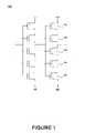
- FIG. 1illustrates a schematic of a stacked inverter delay chain, in accordance with embodiments of the present invention.
- FIG. 2illustrates an exemplary layout of a stacked inverter, in accordance with embodiments of the present invention.
- FIG. 3illustrates a flow chart of steps in a method of delaying a signal, in accordance with embodiments of the present invention.
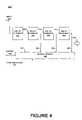
- FIG. 4shows a configurable stacked inverter delay chain in accordance with one embodiment of the present invention.
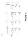
- FIG. 5shows a diagram depicting the internal components of a switch circuit in accordance with one embodiment of the present invention.
- Embodiments of the present inventionimplement a stacked inverter delay chain having delay elements optimized for minimal leakage current.
- the stacked inverter delay chainincludes a plurality of stacked inverter delay elements.
- a switch circuitis included and is coupled to the stacked inverter delay elements and configured to select at least one of the plurality of stacked inverter delay elements to create a delay signal path.
- the delay signal pathhas an amount of delay in accordance with a number of stacked inverter delay elements comprising the delay signal path.
- An inputis coupled to a first stacked inverter delay element of the delay signal path to receive an input signal and an output is coupled to the switch circuit and is coupled to the delay signal path to receive a delayed version of the input signal after propagating through the delay signal path.
- embodiments in accordance with the present inventionis directed toward delay elements having PFETs (or p-type field effect transistors formed in surface N-wells and/or NFETs (or n-type field effect transistors) formed in surface P-wells when a p-type substrate and an N-well process are utilized. It is to be appreciated, however, that embodiments in accordance with the present invention are equally applicable to NFETs formed in surface P-wells and/or PFETs formed in surface N-wells when an n-type substrate and a P-well process are utilized. Consequently, embodiments in accordance with the present invention are well suited to semiconductors formed in both p-type and n-type materials, and such embodiments are considered within the scope of the present invention.
- FIG. 1illustrates a schematic of a novel stacked inverter delay chain 100 , in accordance with embodiments of the present invention.
- Stacked inverter delay chain 100comprises stacked inverters 110 and 120 .
- the output of stacked inverter 110is coupled to the input of stacked inverter 120 .
- additional stacked inverter delay chainse.g., one or more instances of stacked inverter delay chain 100
- can be coupled to stacked inverter delay chain 100 to achieve larger signal delay values. Examples of multiple stacked inverter delay chains arranged a large configurable stacked inverter delay system in accordance with embodiments of the present inventionare described in the discussion of FIG. 4 below.
- stacked inverters 110 and 120comprise more than a single p-type device coupled to a single n-type device. Rather, stacked inverters 110 and 120 comprise multiple p-type devices and multiple n-type devices. More particularly, stacked inverter 120 comprises two p-type devices 121 and 122 and three n-type devices 123 , 124 and 125 . The gates of the devices of stacked inverter 120 are coupled together forming the input of the inverter stage. The output of the inverter stage may be taken at the coupling of a p-type device to an n-type device.
- stacked inverter 120comprises multiple series devices per “leg.” For example, two p-type devices are configured to pull the output high (when appropriate) and three n-type devices are configured to pull the output low. Consequently, the drive capability of stacked inverter 120 is less than the drive capability of a conventional inverter. Beneficially, such decreased drive capability produces an increased delay of a signal through stacked inverter 120 .
- stacked inverter 120presents an increased load to its driving circuitry, in comparison to a conventional inverter.
- a signal input to stacked inverter 120is coupled to five active devices as opposed to being coupled to two active devices in a conventional inverter.
- Each devicepresents an input capacitance.
- Such increased loadingproduces a further desirable increase in signal propagation delay.
- An approximate analysis of stacked inverter delay chain 100indicates that the delay of stacked inverter 120 is about six times the delay of a conventional two-device inverter.
- drive resistance of stacked inverter 120can be about 2.5 times the drive resistance of a conventional inverter
- load capacitance of stacked inverter 120can be about 2.5 times the load capacitance of a conventional inverter.
- stacked inverter 110is constructed similarly, the delay through stacked inverter delay chain 100 will be about 6 times longer than through a conventional inverter pair.
- a delay through stacked inverter delay chain 100is approximately the same as a delay through a chain of 12 stages of conventional inverters. It is appreciated that an exact evaluation is the province of circuit simulation and the details of a particular semiconductor manufacturing process.
- a chain of 12 conventional inverters comprising 24 active deviceshas approximately the same delay as stacked inverter delay chain 100 comprising ten active devices. Consequently, the active switching power of stacked inverter delay chain 100 is beneficially reduced to approximately 42 percent (10 divided by 24) of the active switching power of a conventional delay circuit, for about the same delay.
- stacked inverter delay chain 100comprises about 42 percent of the die area for active devices versus a conventional delay circuit, for approximately the same delay.
- stacked inverter delay chain 100comprises about 42 percent of the die area for active devices versus a conventional delay circuit, for approximately the same delay.
- FIG. 2illustrates an exemplary layout of stacked inverter 120 , in accordance with embodiments of the present invention. It is appreciated that FIG. 2 is not drawn to scale.
- Stacked inverter 120comprises two p-type devices ( 121 , 122 of FIG. 1 ) formed in p-type diffusion within n-well 220 .
- Stacked inverter 120comprises three n-type devices ( 123 , 124 , 125 of FIG. 1 ) formed in n-type diffusion.
- Metallization 240couples p-type diffusion 220 with n-type diffusion 235 , coupling p-type device 122 ( FIG. 1 ) with n-type device 123 ( FIG. 1 ) and forming the output of stacked inverter 120 ( FIG. 1 ).
- Metallization 260couples p-type device 121 ( FIG. 1 ) to an operating voltage, e.g., Vdd.
- Metallization 250couples n-type device 125 ( FIG. 1 ) to ground.
- Metallization 270couples an input signal to the gates of all devices.
- a conventional art inverter chainrequires about 5 contacts per stage.
- a conventional art inverter stagewould typically comprise one contact to couple Vdd to the p-type device, one contact to couple ground to the n-type device, one contact to couple the inverter output to the p-type device, one to couple the inverter output to the n-type device and one contact for the input. Twelve stages of inverters thus require about 60 contacts. It is appreciated that additional contacts are generally required for coupling Vdd and ground to the wells.
- stacked inverter delay chain 100requires far fewer contacts to produce about the same delay as a conventional 12-stage inverter delay chain.
- stacked inverter 120has no need of contacts within its stacks. For example, no contact is necessary between p-type devices 121 and 122 ( FIG. 1 ), nor is a contact necessary between n-type devices 123 and 124 ( FIG. 1 ), nor is a contact necessary between n-type devices 124 and 125 ( FIG. 1 ).
- one contactcouples p-type device 121 ( FIG. 1 ) to Vdd (contact 209 ), and one contact couples n-type device 125 ( FIG. 1 ) to ground (contact 210 ).
- stacked inverter 120can be constructed utilizing a total of about five contacts.
- Exemplary contacts 201 - 208are illustrated coupling Vdd and ground to the wells. It is appreciated that such contacts are commonly interspersed at intervals, e.g., every tenth row of logic, and thus may not be strongly associated with a particular circuit.
- stacked inverter delay chain 100requires only about 10 contacts, or one sixth as many contacts to produce about the same delay. Consequently, embodiments in accordance with the present invention yield highly advantageous integrated circuit die area reductions far beyond a reduction in transistor count.
- a further benefit of stacked inverter delay chain 100derives from utilizing fewer stages in comparison to the conventional art. Consequently, embodiments in accordance with the present invention require less wiring to intercouple stages and fewer inter-stage spaces to separate stages. Such requirements for less wiring and less space result in a desirable reduction in integrated circuit die area required for such wiring and spaces.
- static power consumption in modern semiconductor processese.g., processes with a minimum feature size of about 0.13 microns and smaller, is no longer a negligible component of total power consumption.
- static powermay be one-half of total power consumption.
- static poweras a percentage of total power, is tending to increase with successive generations of semiconductor process.
- Embodiments in accordance with the present inventionoffer significant advantages in reducing static power consumption in comparison with the conventional art.
- a conventional art inverter delay chaincomprises a leakage path for each inverter, e.g., a series “string” of devices from operating voltage (Vdd) to ground.
- Vddoperating voltage
- a 12 inverter delay chaincomprises 12 leakage paths.
- stacked inverter delay chain 100comprises just two leakage paths. Consequently, stacked inverter delay chain 100 comprises one sixth of the leakage paths.
- leakage paths within stacked inverter delay chain 100suffer less leakage than conventional inverters, yielding additional beneficial leakage reductions.
- a conventional inverterexactly one transistor is on while the other transistor is off. As an unfortunate consequence, approximately the full bias voltage is applied to the off transistor, resulting in a maximum possible leakage for the off transistor.
- each off transistorhas significantly less than full bias voltage applied.
- each transistor 123 , 124 and 125will have about one third of full bias voltage applied.
- leakage currentgenerally decreases exponentially as voltage decreases. For example, a two times reduction in off bias voltage produces about an eight times reduction in leakage current per leakage path.
- leakageinduces non zero voltages at intermediate nodes between the off transistors, e.g., between transistors 125 and 124 , and between transistors 124 and 123 .
- Such voltagesinduce body effects in the transistors.
- Such body effectsincrease the threshold voltage of the affected transistors.
- An increased threshold voltagegenerally produces beneficial decreases in leakage current.
- the leakage current of each pathis very beneficially reduced due to an induced body effect and a highly non-linear relationship between bias voltage and leakage current.
- An approximate analysisindicates that total leakage current of stacked inverter delay chain 100 is reduced about 50 times in comparison to a conventional delay chain of inverters, for the same delay.
- delay circuitsAnother aspect of merit regarding delay circuits is the ability of a delay circuit to track speed changes of other circuitry of an integrated circuit. It is appreciated that a variety of factors, e.g., operating voltage, operating temperature and/or manufacturing process variations, can affect the speed of operation of an integrated circuit. It is generally desirable for a delay circuit to track speed changes of other circuitry of an integrated circuit. For example, if other circuits of an integrated circuit operate faster, generally less absolute delay is required from a delay circuit for the overall circuit to function. Because embodiments in accordance with the present invention comprise stacked devices, they are similar to many logic circuits that also comprise stacked devices, e.g., NAND and/or NOR logic gates. Consequently, embodiments in accordance with the present invention match or track changes in operating speed of complex logic more accurately than delay chains comprising very simple inverters.
- Embodiments in accordance with the present inventionare thus shown to offer significant and highly beneficial improvements in tracking timing changes of other circuits, integrated circuit die area, active power consumption and static power (leakage current) consumption in comparison to the conventional art.
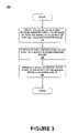
- FIG. 3illustrates a flow chart of steps in a method of delaying a signal 300 , in accordance with embodiments of the present invention.
- the signalis inverted using a first stacked inverter circuit to produce an inverted signal at an output of the first stacked inverter circuit.
- the inverted signalis the output of stacked inverter chain 110 of FIG. 1 .
- the inverted signalis propagated to an input of a second stacked inverter circuit, e.g., at the input of stacked inverter chain 120 of FIG. 1 .
- a delayed version of the signalis produced at an output of the second stacked inverter circuit.
- a delayed version of the input to stacked inverter circuit 110is produced at the output of stacked inverter chain 110 .
- the first and the second stacked inverter circuitscomprise at least five active devices.
- a delay circuitcomprising multiple stacked inverter circuits, each comprising three or more p-type devices in conjunction with three or more n-type devices, may better optimize available resources than stacked inverter delay circuit 100 ( FIG. 1 ).
- stacked inverter chain 120comprises stacked transistors without an intermediate buffer, reducing output drive capability and slowing the circuit down. Further, stacked inverter chain 120 comprises multiple inputs that all have the same logical purpose, increasing input capacitance and further slowing the circuit down.
- embodiments in accordance with the present inventionare contrary to the operation of conventional integrated circuit design tools.
- conventional design synthesis toolswill routinely “optimize” redundancy out of a design.
- stacked inverter 120FIG. 1
- conventional design synthesis toolswill routinely reduce stacked inverter 120 to a conventional two-device inverter. Consequently, a designer may be required to take custom efforts to retain and embody a novel stacked inverter in accordance with embodiments of the present invention when utilizing conventional design tools.
- Embodiments in accordance with the present inventionprovide a stacked inverter comprising desirable delay, die area and power characteristics. Further embodiments in accordance with the present invention provide for coupling two stacked inverters together to form a stacked inverter delay chain that is more efficient in terms of die area, active and passive power consumption than conventional delay chains comprising conventional inverters. Still further embodiments in accordance with the present invention provide for stacks of varying numbers of devices per leg of a stacked inverter.
- the delay chain 400includes a plurality of stacked inverter delay elements 401 - 404 .
- the stacked inverter delay elements 401 - 404are coupled in series as shown.
- Each of the stacked inverter delay elements, referred to hereafter as delay elements, 401 - 404is coupled to a switch circuit 440 as shown.
- the switch circuit 440includes an output 420 for providing the resulting output signal 420 to, for example, other external circuits.
- each of the delay elements 401 - 404comprises a leakage efficient stacked inverter delay chain of the configuration described above (e.g., in the discussion FIG. 1 ).
- a delay elementcan comprise a single stacked inverter (e.g., stacked inverter 110 ) or multiple stacked inverters (e.g., the two stacked inverters 110 and 120 comprising stacked inverter chain 100 ). It should be noted that, depending upon the particular requirements of a given application, differing numbers of stacked inverters (e.g., one or more instances of stacked inverter 110 , stacked inverter 120 , etc.), can be arranged to comprise a delay element.
- the configurable stacked inverter delay chain 400provides substantial benefits with regard to tracking timing changes of other circuits, integrated circuit die area, active power consumption and static power (e.g., leakage current) consumption in comparison to the conventional art.
- the switch circuit 440is coupled to the delay elements 401 - 404 and is configured to select at least one of the plurality of delay elements 401 - 404 to create a delay signal path having an amount of delay in accordance with a number of stacked inverter delay elements comprising the delay signal path. For example, to implement a resulting output signal 420 having the smallest amount of delay, the switch circuit 440 would implement a delay signal path including only the first delay element 401 .
- the input signal 410would propagate to the first delay element 401 and incur an amount of delay in accordance with the devices of the first delay element 401 (e.g., as depicted in delay chain 100 of FIG. 1 ).
- the signal emerging from the first delay element 401is selected by a tap 421 of the switch circuit 440 .
- the signalis coupled to the output 420 by the switch circuit 440 as the resulting delayed output signal 420 .
- the switch circuit 440implements a delay signal path including an additional number of the delay elements.
- the amount of delay added to the input signal 410can be substantially doubled by selecting tap 422 of the switch circuit. This causes the input signal 410 to propagate through the delay element 401 to the input 411 of delay element 402 and through delay element 402 before being picked up by the tap 422 .
- the resulting output signal 420will have an added amount of delay including the delay from elements 401 and 402 .
- the switch circuit 440is configured to implement a configurable, adjustable delay signal path by selecting the appropriate one of the taps 421 - 424 .
- the switch circuit 440adjusts the delay signal path by switching delay elements into or out of the delay signal path via one of the taps 421 - 424 .
- the output of the prior delay elementis coupled to the input of a subsequent delay element (e.g., inputs 411 - 413 ) via a substantially direct connection.
- the desired amount of delayis implemented via a configuration input 430 for the switch circuit 440 .
- the configuration input 430can set the switch circuit 440 to increase the delay amount, decrease the delay amount, keep the same delay amount, or the like.
- four delay elements 401 - 404are shown, it should be noted that a larger number of delay elements can be included within the configurable stacked delay element chain 400 to give a larger range of adjustable delay. This is shown in FIG. 4 by the arrow 450 . Similarly, fewer delay elements (e.g., two) can be used for those applications requiring a small range of adjustable delay.
- adjustable delay capabilities of embodiments of the present inventioncan be advantageously used in a number of different applications.
- a high-performance memory applicatione.g., DDR DRAMs
- sampling windows correspond to the rising and falling edges of the strobe signalscan be accurately placed at the center of the stringent rise-and-hold times.
- the rising and falling edges of multiple data signalscan be accurately aligned with nanosecond accuracy (e.g., 1.875 nanoseconds for DDR II 533 DRAM).
- FIG. 5shows a diagram depicting the internal components of the switch circuit 440 in accordance with one embodiment of the present invention.
- each of the taps 421 - 424is activated or deactivated by its associated logic.
- the logicis set up via associated respective configuration bits stored within respective storage elements (e.g., flops) 511 - 514 .
- the first one of the storage elements 511 - 514 storing a logic zeroresults in its correspond tap being selected (e.g., from left to right).
- the switch circuit 440 embodimentif the first through the “Nth” storage elements are 1 (e.g., from left to right), and the N+1 storage element is zero, the corresponding N+1 tap is selected.
- the storage elements 511 - 514are accessed via their respective inputs 501 - 504 .
- the inputs 501 - 504thus comprise the configuration input 430 shown in FIG. 4 , and can be accessed in parallel.
- the configuration bitscan be shifted into the storage elements serially (e.g., from left to right from element 511 to 514 ).
- the switch circuit 440 embodiment of FIG. 5depicts a configuration where there is either one stacked inverter or an odd number of stacked inverters comprising each delay element. As described above, depending upon the number of stacked inverters per delay element, the signal emerging from one delay element to the next delay element will be inverted (e.g., for an odd number of inverter(s) per delay element) or un-inverted (for an even number of inverters per delay element).
- the logic of the switch circuit 440 embodimentis configured for an odd number of stacked inverters, whereby the inversion is properly handled by the depicted NOR gates. However, for example, for an even number of inverters per delay element, the NOR gates would be replaced by OR gates.
Landscapes
- Physics & Mathematics (AREA)
- Nonlinear Science (AREA)
- Pulse Circuits (AREA)
Abstract
Description
Claims (24)
Priority Applications (1)
| Application Number | Priority Date | Filing Date | Title |
|---|---|---|---|
| US12/002,988US7592842B2 (en) | 2004-12-23 | 2007-12-18 | Configurable delay chain with stacked inverter delay elements |
Applications Claiming Priority (2)
| Application Number | Priority Date | Filing Date | Title |
|---|---|---|---|
| US11/020,746US7310008B1 (en) | 2004-06-08 | 2004-12-23 | Configurable delay chain with stacked inverter delay elements |
| US12/002,988US7592842B2 (en) | 2004-12-23 | 2007-12-18 | Configurable delay chain with stacked inverter delay elements |
Related Parent Applications (1)
| Application Number | Title | Priority Date | Filing Date |
|---|---|---|---|
| US11/020,746ContinuationUS7310008B1 (en) | 2004-06-08 | 2004-12-23 | Configurable delay chain with stacked inverter delay elements |
Publications (2)
| Publication Number | Publication Date |
|---|---|
| US20080129342A1 US20080129342A1 (en) | 2008-06-05 |
| US7592842B2true US7592842B2 (en) | 2009-09-22 |
Family
ID=39474979
Family Applications (1)
| Application Number | Title | Priority Date | Filing Date |
|---|---|---|---|
| US12/002,988Expired - LifetimeUS7592842B2 (en) | 2004-12-23 | 2007-12-18 | Configurable delay chain with stacked inverter delay elements |
Country Status (1)
| Country | Link |
|---|---|
| US (1) | US7592842B2 (en) |
Cited By (2)
| Publication number | Priority date | Publication date | Assignee | Title |
|---|---|---|---|---|
| US9912322B2 (en) | 2013-07-03 | 2018-03-06 | Nvidia Corporation | Clock generation circuit that tracks critical path across process, voltage and temperature variation |
| US10103719B2 (en) | 2013-07-22 | 2018-10-16 | Nvidia Corporation | Integrated voltage regulator with in-built process, temperature and aging compensation |
Families Citing this family (2)
| Publication number | Priority date | Publication date | Assignee | Title |
|---|---|---|---|---|
| KR20140073929A (en)* | 2012-12-07 | 2014-06-17 | 삼성전자주식회사 | Multi-core processor, device having the same, and method for operating the multi-core processor |
| US10254783B2 (en) | 2017-06-28 | 2019-04-09 | Western Digital Technologies, Inc. | External clock based clock generator |
Citations (135)
| Publication number | Priority date | Publication date | Assignee | Title |
|---|---|---|---|---|
| US3991380A (en) | 1976-02-09 | 1976-11-09 | Rca Corporation | Complementary field effect transistor differential amplifier |
| US4498021A (en) | 1982-07-13 | 1985-02-05 | Matsushita Electric Industrial Co., Ltd. | Booster for transmitting digital signal |
| US4700089A (en) | 1984-08-23 | 1987-10-13 | Fujitsu Limited | Delay circuit for gate-array LSI |
| US4739252A (en) | 1986-04-24 | 1988-04-19 | International Business Machines Corporation | Current attenuator useful in a very low leakage current measuring device |
| US4760279A (en) | 1986-07-02 | 1988-07-26 | Kabushiki Kaisha Toshiba | Noise cancelling circuit |
| JPH0389624A (en) | 1989-08-31 | 1991-04-15 | Fujitsu Ltd | semiconductor integrated circuit |
| US5039893A (en) | 1984-07-31 | 1991-08-13 | Yamaha Corporation | Signal delay device |
| US5128560A (en) | 1991-03-22 | 1992-07-07 | Micron Technology, Inc. | Boosted supply output driver circuit for driving an all N-channel output stage |
| JPH0491516U (en) | 1990-12-26 | 1992-08-10 | ||
| US5166555A (en) | 1990-05-31 | 1992-11-24 | Nec Corporation | Drive circuit comprising a subsidiary drive circuit |
| US5227679A (en) | 1992-01-02 | 1993-07-13 | Advanced Micro Devices, Inc. | Cmos digital-controlled delay gate |
| US5264738A (en) | 1991-05-31 | 1993-11-23 | U.S. Philips Corp. | Flip-flop circuit having transfer gate delay |
| US5297086A (en) | 1990-07-31 | 1994-03-22 | Texas Instruments Incorporated | Method for initializing redundant circuitry |
| JPH06216723A (en) | 1993-01-14 | 1994-08-05 | Toshiba Corp | Semiconductor integrated circuit |
| US5410278A (en) | 1991-12-19 | 1995-04-25 | Sharp Kabushiki Kaisha | Ring oscillator having a variable oscillating frequency |
| US5414312A (en) | 1993-07-15 | 1995-05-09 | Altera Corporation | Advanced signal driving buffer with directional input transition detection |
| US5455521A (en) | 1993-10-22 | 1995-10-03 | The Board Of Trustees Of The Leland Stanford Junior University | Self-timed interconnect speed-up circuit |
| US5467038A (en) | 1994-02-15 | 1995-11-14 | Hewlett-Packard Company | Quick resolving latch |
| US5497105A (en) | 1994-06-30 | 1996-03-05 | Vlsi Technology, Inc. | Programmable output pad with circuitry for reducing ground bounce noise and power supply noise and method therefor |
| US5525616A (en) | 1993-05-13 | 1996-06-11 | Monsanto Company | Method of inhibiting glycolipid synthesis |
| US5568103A (en) | 1994-12-28 | 1996-10-22 | Mitsubishi Electric Engineering Co., Ltd. | Current control circuit of ring oscillator |
| US5587665A (en) | 1995-07-18 | 1996-12-24 | Vlsi Technology, Inc. | Testing hot carrier induced degradation to fall and rise time of CMOS inverter circuits |
| US5594360A (en) | 1994-10-19 | 1997-01-14 | Intel Corporation | Low current reduced area programming voltage detector for flash memory |
| US5610548A (en) | 1995-09-08 | 1997-03-11 | International Business Machines Corporation | Split drive clock buffer |
| US5614845A (en) | 1995-09-08 | 1997-03-25 | International Business Machines Corporation | Independent clock edge regulation |
| US5656963A (en) | 1995-09-08 | 1997-08-12 | International Business Machines Corporation | Clock distribution network for reducing clock skew |
| US5677650A (en) | 1995-12-19 | 1997-10-14 | Pmc-Sierra, Inc. | Ring oscillator having a substantially sinusoidal signal |
| US5680359A (en) | 1995-03-24 | 1997-10-21 | Hyundai Electronics Industries Co., Ltd. | Self-refresh period adjustment circuit for semiconductor memory device |
| US5698994A (en) | 1994-07-29 | 1997-12-16 | Nkk Corporation | Data output circuit, intermediate potential setting circuit, and semiconductor integrated circuit |
| US5739715A (en) | 1995-10-31 | 1998-04-14 | Hewlett-Packard Co. | Digital signal driver circuit having a high slew rate |
| US5764110A (en) | 1996-07-15 | 1998-06-09 | Mitsubishi Denki Kabushiki Kaisha | Voltage controlled ring oscillator stabilized against supply voltage fluctuations |
| US5767700A (en) | 1995-06-30 | 1998-06-16 | Hyundai Electronics Industries Co., Ltd. | Pulse signal transfer unit employing post charge logic |
| US5778214A (en) | 1994-12-09 | 1998-07-07 | Oki Electric Industry Co., Ltd. | Bit-phase aligning circuit |
| US5777501A (en) | 1996-04-29 | 1998-07-07 | Mosaid Technologies Incorporated | Digital delay line for a reduced jitter digital delay lock loop |
| US5791715A (en) | 1996-11-22 | 1998-08-11 | Nebel; Michael W. | Extension mechanism for travel trailer slide-out rooms |
| US5793715A (en) | 1995-11-15 | 1998-08-11 | Zen Research N.V. | Methods and apparatus for reducing the access time of an optical drive |
| US5796313A (en) | 1996-04-25 | 1998-08-18 | Waferscale Integration Inc. | Low power programmable ring oscillator |
| US5797105A (en) | 1994-08-23 | 1998-08-18 | National Aerospace Laboratory Of Science & Technology | Air active control aircraft using three dimensional true airspeed detection system |
| US5811983A (en) | 1996-09-03 | 1998-09-22 | Integrated Device Technology, Inc. | Test ring oscillator |
| US5880608A (en) | 1996-12-27 | 1999-03-09 | Intel Corporation | Pulsed domino latches |
| US5894419A (en) | 1997-04-21 | 1999-04-13 | International Business Machines Corporation | System and method for robust clocking schemes for logic circuits |
| US5926050A (en) | 1996-07-29 | 1999-07-20 | Townsend And Townsend And Crew Llp | Separate set/reset paths for time critical signals |
| US5963043A (en) | 1997-09-17 | 1999-10-05 | International Business Machines Corporation | Method and apparatus for characterized parasitic capacitance between integrated-circuit interconnects |
| US5963074A (en)* | 1997-06-18 | 1999-10-05 | Credence Systems Corporation | Programmable delay circuit having calibratable delays |
| US5969543A (en) | 1995-09-15 | 1999-10-19 | Xilinx, Inc. | Input signal interface with independently controllable pull-up and pull-down circuitry |
| US5977763A (en) | 1996-02-27 | 1999-11-02 | Micron Technology, Inc. | Circuit and method for measuring and forcing an internal voltage of an integrated circuit |
| US5982211A (en) | 1997-03-31 | 1999-11-09 | Texas Instruments Incorporated | Hybrid dual threshold transistor registers |
| US6011403A (en) | 1997-10-31 | 2000-01-04 | Credence Systems Corporation | Circuit arrangement for measuring leakage current utilizing a differential integrating capacitor |
| US6025738A (en) | 1997-08-22 | 2000-02-15 | International Business Machines Corporation | Gain enhanced split drive buffer |
| US6028490A (en) | 1997-04-25 | 2000-02-22 | Sony Corporation | Ring oscillators having inverting and delay elements |
| US6031403A (en) | 1996-11-13 | 2000-02-29 | International Business Machines Corporation | Pull-up and pull-down circuits |
| US6069506A (en) | 1998-05-20 | 2000-05-30 | Micron Technology, Inc. | Method and apparatus for improving the performance of digital delay locked loop circuits |
| US6111447A (en) | 1998-05-01 | 2000-08-29 | Vanguard International Semiconductor Corp. | Timing circuit that selectively triggers on a rising or falling input signal edge |
| US6114840A (en) | 1998-09-17 | 2000-09-05 | Integrated Device Technology, Inc. | Signal transfer devices having self-timed booster circuits therein |
| US6127872A (en) | 1997-03-17 | 2000-10-03 | Sony Corporation | Delay circuit and oscillator circuit using the same |
| US6154099A (en) | 1997-10-09 | 2000-11-28 | Kabushiki Kaisha Toshiba | Ring oscillator and method of measuring gate delay time in this ring oscillator |
| US6154100A (en) | 1998-08-31 | 2000-11-28 | Nec Corporation | Ring oscillator and delay circuit using low threshold voltage type MOSFETS |
| US6160755A (en) | 1997-06-17 | 2000-12-12 | Micron Technology, Inc. | Clock signal from an adjustable oscillator for an integrated circuit |
| US6172943B1 (en) | 1997-10-07 | 2001-01-09 | Seiko Instruments Inc. | Electronic clock having an electric power generating element |
| US6172545B1 (en)* | 1997-05-09 | 2001-01-09 | Nec Corporation | Delay circuit on a semiconductor device |
| US6188260B1 (en) | 1999-01-22 | 2001-02-13 | Agilent Technologies | Master-slave flip-flop and method |
| US6198334B1 (en) | 1997-04-24 | 2001-03-06 | Hitachi, Ltd. | CMOS circuit |
| US6204710B1 (en) | 1998-06-22 | 2001-03-20 | Xilinx, Inc. | Precision trim circuit for delay lines |
| US20010000426A1 (en) | 1999-01-08 | 2001-04-26 | Altera Corporation | Phase-locked loop or delay-locked loop circuitry for programmable logic devices |
| US6229747B1 (en) | 1998-12-23 | 2001-05-08 | Hyundai Electronics Industries Co., Ltd. | Self-refresh apparatus for a semiconductor memory device |
| US6242936B1 (en) | 1998-08-11 | 2001-06-05 | Texas Instruments Incorporated | Circuit for driving conductive line and testing conductive line for current leakage |
| US6242937B1 (en) | 1999-02-12 | 2001-06-05 | Hyundai Electronics Industries Co., Ltd. | Hot carrier measuring circuit |
| US6262601B1 (en) | 1999-06-25 | 2001-07-17 | Hyundai Electronics Industries Co., Ltd. | Inverter for high voltage full swing output |
| US6275091B1 (en) | 1999-07-23 | 2001-08-14 | Nec Corporation | Clock signal control circuit and method and synchronous delay circuit |
| US6281706B1 (en) | 1998-03-30 | 2001-08-28 | National Semiconductor Corp. | Programmable high speed quiet I/O cell |
| US6285230B1 (en) | 1999-04-07 | 2001-09-04 | Hyundai Electronics Industries Co., Ltd. | Input buffer circuit with adjustable delay via an external power voltage |
| US6294930B1 (en) | 1997-04-11 | 2001-09-25 | Xilinx, Inc. | FPGA with a plurality of input reference voltage levels |
| US20010028278A1 (en) | 1995-06-12 | 2001-10-11 | Mitsubishi Denki Kabushiki Kaisha | Temperature dependent circuit, and current generating circuit, inverter and oscillation circuit using the same |
| US20010030561A1 (en) | 2000-02-07 | 2001-10-18 | Hideo Asano | Signal output device and method for sending signals at multiple transfer rates while minimizing crosstalk effects |
| US6321282B1 (en) | 1999-10-19 | 2001-11-20 | Rambus Inc. | Apparatus and method for topography dependent signaling |
| US6323706B1 (en) | 2000-02-24 | 2001-11-27 | Rambus Inc. | Apparatus and method for edge based duty cycle conversion |
| US20010052623A1 (en) | 2000-03-30 | 2001-12-20 | Atsushi Kameyama | Semiconductor integrated circuit |
| US6366115B1 (en) | 2001-02-21 | 2002-04-02 | Analog Devices, Inc. | Buffer circuit with rising and falling edge propagation delay correction and method |
| US6407571B1 (en) | 1999-04-14 | 2002-06-18 | Matsushita Electric Industrial Co., Ltd. | Voltage detecting circuit for a power system |
| US6426652B1 (en) | 2001-05-14 | 2002-07-30 | Sun Microsystems, Inc. | Dual-edge triggered dynamic logic |
| US6426641B1 (en) | 1998-10-21 | 2002-07-30 | International Business Machines Corporation | Single pin performance screen ring oscillator with frequency division |
| US6459319B2 (en) | 2000-05-26 | 2002-10-01 | Fujitsu Limited | Variable delay circuit and semiconductor integrated circuit having the same |
| US6466063B2 (en) | 2001-03-20 | 2002-10-15 | Taiwan Semiconductor Manufacturing Co., Ltd. | Push-pull output buffer with gate voltage feedback loop |
| US6476632B1 (en) | 2000-06-22 | 2002-11-05 | International Business Machines Corporation | Ring oscillator design for MOSFET device reliability investigations and its use for in-line monitoring |
| US20020178415A1 (en) | 2001-03-30 | 2002-11-28 | Ritesh Saraf | Skewed latch flip-flop with embedded scan function |
| US6489796B2 (en) | 2000-06-30 | 2002-12-03 | Mitsubishi Denki Kabushiki Kaisha | Semiconductor device provided with boost circuit consuming less current |
| US20030005775A1 (en) | 2001-07-09 | 2003-01-09 | Nartron Corporation | Compressible capacitance sensor for determining the presence of an object |
| US20030011413A1 (en) | 2001-06-29 | 2003-01-16 | Masleid Robert P. | Low latency clock distribution |
| US20030042960A1 (en)* | 2001-08-29 | 2003-03-06 | Gomm Tyler J. | Variable delay circuit and method, and delay locked loop, memory device and computer system using same |
| US6535014B2 (en) | 2000-01-19 | 2003-03-18 | Lucent Technologies, Inc. | Electrical parameter tester having decoupling means |
| US6538522B1 (en) | 2001-10-15 | 2003-03-25 | International Business Machines Corporation | Method and ring oscillator for evaluating dynamic circuits |
| US6538471B1 (en) | 2001-10-10 | 2003-03-25 | International Business Machines Corporation | Multi-threshold flip-flop circuit having an outside feedback |
| US20030057775A1 (en) | 2001-09-26 | 2003-03-27 | Takekazu Yamashita | Semiconductor integrated circuit and multi-chip package |
| US6545519B1 (en) | 2002-03-28 | 2003-04-08 | International Business Machines Corporation | Level shifting, scannable latch, and method therefor |
| US6570407B1 (en) | 2002-01-30 | 2003-05-27 | Sun Microsystems, Inc. | Scannable latch for a dynamic circuit |
| US6573777B2 (en) | 2001-06-29 | 2003-06-03 | Intel Corporation | Variable-delay element with an inverter and a digitally adjustable resistor |
| US6577157B1 (en) | 1997-11-14 | 2003-06-10 | Altera Corporation | Fully programmable I/O pin with memory |
| US6577176B1 (en) | 2002-06-12 | 2003-06-10 | Fujitsu Limited | Complement reset latch |
| US20030160630A1 (en) | 2002-02-27 | 2003-08-28 | Adrian Earle | Bidirectional edge accelerator circuit |
| US6621318B1 (en) | 2001-06-01 | 2003-09-16 | Sun Microsystems, Inc. | Low voltage latch with uniform sizing |
| US20030189465A1 (en) | 2002-04-09 | 2003-10-09 | International Business Machines Corporation | System and method for measuring circuit performance degradation due to PFET negative bias temperature instability (NBTI) |
| US6657504B1 (en) | 2002-04-30 | 2003-12-02 | Unisys Corporation | System and method of determining ring oscillator speed |
| US6664837B1 (en) | 2002-09-18 | 2003-12-16 | Xilinx, Inc. | Delay line trim unit having consistent performance under varying process and temperature conditions |
| US20030231713A1 (en) | 2002-06-12 | 2003-12-18 | Masleid Robert P. | Complement reset buffer |
| US6690242B2 (en) | 2001-12-21 | 2004-02-10 | Texas Instruments Incorporated | Delay circuit with current steering output symmetry and supply voltage insensitivity |
| US6697929B1 (en) | 2000-02-14 | 2004-02-24 | Intel Corporation | Scannable zero-catcher and one-catcher circuits for reduced clock loading and power dissipation |
| EP1398639A2 (en) | 2002-09-13 | 2004-03-17 | Chartered Semiconductor Manufacturing Pte Ltd. | Test structures for on-chip real-time reliability testing |
| US20040104731A1 (en) | 2002-11-29 | 2004-06-03 | Rolf-P. Vollertsen | Method of reliability testing |
| US20040119501A1 (en) | 2002-12-23 | 2004-06-24 | Sabbavarapu Anil K. | Scan cell systems and methods |
| US20040119503A1 (en) | 2002-12-18 | 2004-06-24 | Shahram Jamshidi | Gate-clocked domino circuits with reduced leakage current |
| US20040124900A1 (en)* | 2002-09-11 | 2004-07-01 | Infineon Technologies Ag | Digital signal delay device |
| US6759863B2 (en) | 2000-05-15 | 2004-07-06 | The Governors Of The University Of Alberta | Wireless radio frequency technique design and method for testing of integrated circuits and wafers |
| US6762638B2 (en) | 2002-10-16 | 2004-07-13 | International Business Machines Corporation | Circuit for preserving data in a flip-flop and a method of use |
| US6762966B1 (en) | 2003-01-08 | 2004-07-13 | International Business Machines Corporation | Method and circuit to investigate charge transfer array transistor characteristics and aging under realistic stress and its implementation to DRAM MOSFET array transistor |
| US6768363B2 (en) | 2002-04-03 | 2004-07-27 | Samsung Electronics, Co. Ltd. | Output driver circuit for controlling up-slew rate and down-slew rate independently and up-driving strength and down-driving strength independently |
| US20040148111A1 (en) | 2003-01-23 | 2004-07-29 | Gauthier Claude R. | Embedded integrated circuit aging sensor System |
| US6774734B2 (en) | 2002-11-27 | 2004-08-10 | International Business Machines Corporation | Ring oscillator circuit for EDRAM/DRAM performance monitoring |
| US6798230B1 (en) | 2003-01-15 | 2004-09-28 | Advanced Micro Devices, Inc. | Structure and method for increasing accuracy in predicting hot carrier injection (HCI) degradation in semiconductor devices |
| US6815971B2 (en) | 2002-11-06 | 2004-11-09 | Taiwan Semiconductor Manufacturing Co., Ltd | Method and apparatus for stress testing integrated circuits using an adjustable AC hot carrier injection source |
| US6831494B1 (en) | 2003-05-16 | 2004-12-14 | Transmeta Corporation | Voltage compensated integrated circuits |
| US20040257115A1 (en) | 2003-04-28 | 2004-12-23 | Via Technologies, Inc. | N-domino output latch with accelerated evaluate path |
| US6879200B2 (en) | 2001-03-28 | 2005-04-12 | Fujitsu Limited | Delay circuit, semiconductor integrated circuit device containing a delay circuit and delay method |
| US6882172B1 (en) | 2002-04-16 | 2005-04-19 | Transmeta Corporation | System and method for measuring transistor leakage current with a ring oscillator |
| US6903564B1 (en) | 2003-11-12 | 2005-06-07 | Transmeta Corporation | Device aging determination circuit |
| US6924669B2 (en) | 2000-03-30 | 2005-08-02 | Fujitsu Limited | Output buffer circuit and control method therefor |
| US20050184720A1 (en) | 2003-01-24 | 2005-08-25 | International Business Machines Corporation | Circuitry and methodology to establish correlation between gate dielectric test site reliability and product gate reliability |
| US20050212547A1 (en) | 2002-04-16 | 2005-09-29 | Shingo Suzuki | System and method for measuring time dependent dielectric breakdown with a ring oscillator |
| US20050248368A1 (en) | 2003-04-28 | 2005-11-10 | Via Technologies, Inc. | P-domino output latch with accelerated evaluate path |
| US7119580B2 (en) | 2004-06-08 | 2006-10-10 | Transmeta Corporation | Repeater circuit with high performance repeater mode and normal repeater mode |
| US7142018B2 (en) | 2004-06-08 | 2006-11-28 | Transmeta Corporation | Circuits and methods for detecting and assisting wire transitions |
| US7173455B2 (en) | 2004-06-08 | 2007-02-06 | Transmeta Corporation | Repeater circuit having different operating and reset voltage ranges, and methods thereof |
| US7239170B2 (en) | 2003-07-08 | 2007-07-03 | Lsi Corporation | Apparatus and methods for improved input/output cells |
| US7271638B2 (en) | 2003-07-31 | 2007-09-18 | Elpida Memory, Inc. | Delay circuit and delay synchronization loop device |
| US7304503B2 (en) | 2004-06-08 | 2007-12-04 | Transmeta Corporation | Repeater circuit with high performance repeater mode and normal repeater mode, wherein high performance repeater mode has fast reset capability |
| US7336103B1 (en) | 2004-06-08 | 2008-02-26 | Transmeta Corporation | Stacked inverter delay chain |
- 2007
- 2007-12-18USUS12/002,988patent/US7592842B2/ennot_activeExpired - Lifetime
Patent Citations (146)
| Publication number | Priority date | Publication date | Assignee | Title |
|---|---|---|---|---|
| US3991380A (en) | 1976-02-09 | 1976-11-09 | Rca Corporation | Complementary field effect transistor differential amplifier |
| US4498021A (en) | 1982-07-13 | 1985-02-05 | Matsushita Electric Industrial Co., Ltd. | Booster for transmitting digital signal |
| US5039893A (en) | 1984-07-31 | 1991-08-13 | Yamaha Corporation | Signal delay device |
| US4700089A (en) | 1984-08-23 | 1987-10-13 | Fujitsu Limited | Delay circuit for gate-array LSI |
| US4739252A (en) | 1986-04-24 | 1988-04-19 | International Business Machines Corporation | Current attenuator useful in a very low leakage current measuring device |
| US4760279A (en) | 1986-07-02 | 1988-07-26 | Kabushiki Kaisha Toshiba | Noise cancelling circuit |
| JPH0389624A (en) | 1989-08-31 | 1991-04-15 | Fujitsu Ltd | semiconductor integrated circuit |
| US5166555A (en) | 1990-05-31 | 1992-11-24 | Nec Corporation | Drive circuit comprising a subsidiary drive circuit |
| US5297086A (en) | 1990-07-31 | 1994-03-22 | Texas Instruments Incorporated | Method for initializing redundant circuitry |
| JPH0491516U (en) | 1990-12-26 | 1992-08-10 | ||
| US5128560A (en) | 1991-03-22 | 1992-07-07 | Micron Technology, Inc. | Boosted supply output driver circuit for driving an all N-channel output stage |
| US5264738A (en) | 1991-05-31 | 1993-11-23 | U.S. Philips Corp. | Flip-flop circuit having transfer gate delay |
| US5410278A (en) | 1991-12-19 | 1995-04-25 | Sharp Kabushiki Kaisha | Ring oscillator having a variable oscillating frequency |
| US5227679A (en) | 1992-01-02 | 1993-07-13 | Advanced Micro Devices, Inc. | Cmos digital-controlled delay gate |
| JPH06216723A (en) | 1993-01-14 | 1994-08-05 | Toshiba Corp | Semiconductor integrated circuit |
| US5525616A (en) | 1993-05-13 | 1996-06-11 | Monsanto Company | Method of inhibiting glycolipid synthesis |
| US5414312A (en) | 1993-07-15 | 1995-05-09 | Altera Corporation | Advanced signal driving buffer with directional input transition detection |
| US5455521A (en) | 1993-10-22 | 1995-10-03 | The Board Of Trustees Of The Leland Stanford Junior University | Self-timed interconnect speed-up circuit |
| US5467038A (en) | 1994-02-15 | 1995-11-14 | Hewlett-Packard Company | Quick resolving latch |
| US5497105A (en) | 1994-06-30 | 1996-03-05 | Vlsi Technology, Inc. | Programmable output pad with circuitry for reducing ground bounce noise and power supply noise and method therefor |
| US5698994A (en) | 1994-07-29 | 1997-12-16 | Nkk Corporation | Data output circuit, intermediate potential setting circuit, and semiconductor integrated circuit |
| US5797105A (en) | 1994-08-23 | 1998-08-18 | National Aerospace Laboratory Of Science & Technology | Air active control aircraft using three dimensional true airspeed detection system |
| US5594360A (en) | 1994-10-19 | 1997-01-14 | Intel Corporation | Low current reduced area programming voltage detector for flash memory |
| US5778214A (en) | 1994-12-09 | 1998-07-07 | Oki Electric Industry Co., Ltd. | Bit-phase aligning circuit |
| US5568103A (en) | 1994-12-28 | 1996-10-22 | Mitsubishi Electric Engineering Co., Ltd. | Current control circuit of ring oscillator |
| US5680359A (en) | 1995-03-24 | 1997-10-21 | Hyundai Electronics Industries Co., Ltd. | Self-refresh period adjustment circuit for semiconductor memory device |
| US20010028278A1 (en) | 1995-06-12 | 2001-10-11 | Mitsubishi Denki Kabushiki Kaisha | Temperature dependent circuit, and current generating circuit, inverter and oscillation circuit using the same |
| US5767700A (en) | 1995-06-30 | 1998-06-16 | Hyundai Electronics Industries Co., Ltd. | Pulse signal transfer unit employing post charge logic |
| US5587665A (en) | 1995-07-18 | 1996-12-24 | Vlsi Technology, Inc. | Testing hot carrier induced degradation to fall and rise time of CMOS inverter circuits |
| US5614845A (en) | 1995-09-08 | 1997-03-25 | International Business Machines Corporation | Independent clock edge regulation |
| US5656963A (en) | 1995-09-08 | 1997-08-12 | International Business Machines Corporation | Clock distribution network for reducing clock skew |
| US5610548A (en) | 1995-09-08 | 1997-03-11 | International Business Machines Corporation | Split drive clock buffer |
| US5969543A (en) | 1995-09-15 | 1999-10-19 | Xilinx, Inc. | Input signal interface with independently controllable pull-up and pull-down circuitry |
| US5739715A (en) | 1995-10-31 | 1998-04-14 | Hewlett-Packard Co. | Digital signal driver circuit having a high slew rate |
| US5793715A (en) | 1995-11-15 | 1998-08-11 | Zen Research N.V. | Methods and apparatus for reducing the access time of an optical drive |
| US5677650A (en) | 1995-12-19 | 1997-10-14 | Pmc-Sierra, Inc. | Ring oscillator having a substantially sinusoidal signal |
| US5977763A (en) | 1996-02-27 | 1999-11-02 | Micron Technology, Inc. | Circuit and method for measuring and forcing an internal voltage of an integrated circuit |
| US5796313A (en) | 1996-04-25 | 1998-08-18 | Waferscale Integration Inc. | Low power programmable ring oscillator |
| US5777501A (en) | 1996-04-29 | 1998-07-07 | Mosaid Technologies Incorporated | Digital delay line for a reduced jitter digital delay lock loop |
| US5764110A (en) | 1996-07-15 | 1998-06-09 | Mitsubishi Denki Kabushiki Kaisha | Voltage controlled ring oscillator stabilized against supply voltage fluctuations |
| US5926050A (en) | 1996-07-29 | 1999-07-20 | Townsend And Townsend And Crew Llp | Separate set/reset paths for time critical signals |
| US5811983A (en) | 1996-09-03 | 1998-09-22 | Integrated Device Technology, Inc. | Test ring oscillator |
| US6031403A (en) | 1996-11-13 | 2000-02-29 | International Business Machines Corporation | Pull-up and pull-down circuits |
| US5791715A (en) | 1996-11-22 | 1998-08-11 | Nebel; Michael W. | Extension mechanism for travel trailer slide-out rooms |
| US5880608A (en) | 1996-12-27 | 1999-03-09 | Intel Corporation | Pulsed domino latches |
| US6127872A (en) | 1997-03-17 | 2000-10-03 | Sony Corporation | Delay circuit and oscillator circuit using the same |
| US5982211A (en) | 1997-03-31 | 1999-11-09 | Texas Instruments Incorporated | Hybrid dual threshold transistor registers |
| US6087886A (en) | 1997-03-31 | 2000-07-11 | Texas Instruments Incorporated | Hybrid dual threshold transistor multiplexer |
| US6294930B1 (en) | 1997-04-11 | 2001-09-25 | Xilinx, Inc. | FPGA with a plurality of input reference voltage levels |
| US5894419A (en) | 1997-04-21 | 1999-04-13 | International Business Machines Corporation | System and method for robust clocking schemes for logic circuits |
| US6198334B1 (en) | 1997-04-24 | 2001-03-06 | Hitachi, Ltd. | CMOS circuit |
| US6028490A (en) | 1997-04-25 | 2000-02-22 | Sony Corporation | Ring oscillators having inverting and delay elements |
| US6172545B1 (en)* | 1997-05-09 | 2001-01-09 | Nec Corporation | Delay circuit on a semiconductor device |
| US6160755A (en) | 1997-06-17 | 2000-12-12 | Micron Technology, Inc. | Clock signal from an adjustable oscillator for an integrated circuit |
| US5963074A (en)* | 1997-06-18 | 1999-10-05 | Credence Systems Corporation | Programmable delay circuit having calibratable delays |
| US6025738A (en) | 1997-08-22 | 2000-02-15 | International Business Machines Corporation | Gain enhanced split drive buffer |
| US5963043A (en) | 1997-09-17 | 1999-10-05 | International Business Machines Corporation | Method and apparatus for characterized parasitic capacitance between integrated-circuit interconnects |
| US6172943B1 (en) | 1997-10-07 | 2001-01-09 | Seiko Instruments Inc. | Electronic clock having an electric power generating element |
| US6154099A (en) | 1997-10-09 | 2000-11-28 | Kabushiki Kaisha Toshiba | Ring oscillator and method of measuring gate delay time in this ring oscillator |
| US6011403A (en) | 1997-10-31 | 2000-01-04 | Credence Systems Corporation | Circuit arrangement for measuring leakage current utilizing a differential integrating capacitor |
| US6577157B1 (en) | 1997-11-14 | 2003-06-10 | Altera Corporation | Fully programmable I/O pin with memory |
| US6281706B1 (en) | 1998-03-30 | 2001-08-28 | National Semiconductor Corp. | Programmable high speed quiet I/O cell |
| US6111447A (en) | 1998-05-01 | 2000-08-29 | Vanguard International Semiconductor Corp. | Timing circuit that selectively triggers on a rising or falling input signal edge |
| US6069506A (en) | 1998-05-20 | 2000-05-30 | Micron Technology, Inc. | Method and apparatus for improving the performance of digital delay locked loop circuits |
| US6204710B1 (en) | 1998-06-22 | 2001-03-20 | Xilinx, Inc. | Precision trim circuit for delay lines |
| US6242936B1 (en) | 1998-08-11 | 2001-06-05 | Texas Instruments Incorporated | Circuit for driving conductive line and testing conductive line for current leakage |
| US6154100A (en) | 1998-08-31 | 2000-11-28 | Nec Corporation | Ring oscillator and delay circuit using low threshold voltage type MOSFETS |
| US6114840A (en) | 1998-09-17 | 2000-09-05 | Integrated Device Technology, Inc. | Signal transfer devices having self-timed booster circuits therein |
| US6426641B1 (en) | 1998-10-21 | 2002-07-30 | International Business Machines Corporation | Single pin performance screen ring oscillator with frequency division |
| US6229747B1 (en) | 1998-12-23 | 2001-05-08 | Hyundai Electronics Industries Co., Ltd. | Self-refresh apparatus for a semiconductor memory device |
| US20010000426A1 (en) | 1999-01-08 | 2001-04-26 | Altera Corporation | Phase-locked loop or delay-locked loop circuitry for programmable logic devices |
| US6188260B1 (en) | 1999-01-22 | 2001-02-13 | Agilent Technologies | Master-slave flip-flop and method |
| US6242937B1 (en) | 1999-02-12 | 2001-06-05 | Hyundai Electronics Industries Co., Ltd. | Hot carrier measuring circuit |
| US6285230B1 (en) | 1999-04-07 | 2001-09-04 | Hyundai Electronics Industries Co., Ltd. | Input buffer circuit with adjustable delay via an external power voltage |
| US6407571B1 (en) | 1999-04-14 | 2002-06-18 | Matsushita Electric Industrial Co., Ltd. | Voltage detecting circuit for a power system |
| US6262601B1 (en) | 1999-06-25 | 2001-07-17 | Hyundai Electronics Industries Co., Ltd. | Inverter for high voltage full swing output |
| US6275091B1 (en) | 1999-07-23 | 2001-08-14 | Nec Corporation | Clock signal control circuit and method and synchronous delay circuit |
| US6321282B1 (en) | 1999-10-19 | 2001-11-20 | Rambus Inc. | Apparatus and method for topography dependent signaling |
| US20020056016A1 (en) | 1999-10-19 | 2002-05-09 | Rambus Inc. | Apparatus and method for topography dependent signaling |
| US6535014B2 (en) | 2000-01-19 | 2003-03-18 | Lucent Technologies, Inc. | Electrical parameter tester having decoupling means |
| US20010030561A1 (en) | 2000-02-07 | 2001-10-18 | Hideo Asano | Signal output device and method for sending signals at multiple transfer rates while minimizing crosstalk effects |
| US6697929B1 (en) | 2000-02-14 | 2004-02-24 | Intel Corporation | Scannable zero-catcher and one-catcher circuits for reduced clock loading and power dissipation |
| US6323706B1 (en) | 2000-02-24 | 2001-11-27 | Rambus Inc. | Apparatus and method for edge based duty cycle conversion |
| US20010052623A1 (en) | 2000-03-30 | 2001-12-20 | Atsushi Kameyama | Semiconductor integrated circuit |
| US7053660B2 (en) | 2000-03-30 | 2006-05-30 | Fujitsu Limited | Output buffer circuit and control method therefor |
| US6455901B2 (en) | 2000-03-30 | 2002-09-24 | Kabushiki Kaisha Toshiba | Semiconductor integrated circuit |
| US6924669B2 (en) | 2000-03-30 | 2005-08-02 | Fujitsu Limited | Output buffer circuit and control method therefor |
| US6759863B2 (en) | 2000-05-15 | 2004-07-06 | The Governors Of The University Of Alberta | Wireless radio frequency technique design and method for testing of integrated circuits and wafers |
| US6459319B2 (en) | 2000-05-26 | 2002-10-01 | Fujitsu Limited | Variable delay circuit and semiconductor integrated circuit having the same |
| US6476632B1 (en) | 2000-06-22 | 2002-11-05 | International Business Machines Corporation | Ring oscillator design for MOSFET device reliability investigations and its use for in-line monitoring |
| US6489796B2 (en) | 2000-06-30 | 2002-12-03 | Mitsubishi Denki Kabushiki Kaisha | Semiconductor device provided with boost circuit consuming less current |
| US6366115B1 (en) | 2001-02-21 | 2002-04-02 | Analog Devices, Inc. | Buffer circuit with rising and falling edge propagation delay correction and method |
| US6466063B2 (en) | 2001-03-20 | 2002-10-15 | Taiwan Semiconductor Manufacturing Co., Ltd. | Push-pull output buffer with gate voltage feedback loop |
| US6879200B2 (en) | 2001-03-28 | 2005-04-12 | Fujitsu Limited | Delay circuit, semiconductor integrated circuit device containing a delay circuit and delay method |
| US20020178415A1 (en) | 2001-03-30 | 2002-11-28 | Ritesh Saraf | Skewed latch flip-flop with embedded scan function |
| US6426652B1 (en) | 2001-05-14 | 2002-07-30 | Sun Microsystems, Inc. | Dual-edge triggered dynamic logic |
| US6621318B1 (en) | 2001-06-01 | 2003-09-16 | Sun Microsystems, Inc. | Low voltage latch with uniform sizing |
| US20030011413A1 (en) | 2001-06-29 | 2003-01-16 | Masleid Robert P. | Low latency clock distribution |
| US6573777B2 (en) | 2001-06-29 | 2003-06-03 | Intel Corporation | Variable-delay element with an inverter and a digitally adjustable resistor |
| US20030005775A1 (en) | 2001-07-09 | 2003-01-09 | Nartron Corporation | Compressible capacitance sensor for determining the presence of an object |
| US20030042960A1 (en)* | 2001-08-29 | 2003-03-06 | Gomm Tyler J. | Variable delay circuit and method, and delay locked loop, memory device and computer system using same |
| US20030057775A1 (en) | 2001-09-26 | 2003-03-27 | Takekazu Yamashita | Semiconductor integrated circuit and multi-chip package |
| US6538471B1 (en) | 2001-10-10 | 2003-03-25 | International Business Machines Corporation | Multi-threshold flip-flop circuit having an outside feedback |
| US6538522B1 (en) | 2001-10-15 | 2003-03-25 | International Business Machines Corporation | Method and ring oscillator for evaluating dynamic circuits |
| US6690242B2 (en) | 2001-12-21 | 2004-02-10 | Texas Instruments Incorporated | Delay circuit with current steering output symmetry and supply voltage insensitivity |
| US6570407B1 (en) | 2002-01-30 | 2003-05-27 | Sun Microsystems, Inc. | Scannable latch for a dynamic circuit |
| US20030160630A1 (en) | 2002-02-27 | 2003-08-28 | Adrian Earle | Bidirectional edge accelerator circuit |
| US6545519B1 (en) | 2002-03-28 | 2003-04-08 | International Business Machines Corporation | Level shifting, scannable latch, and method therefor |
| US6768363B2 (en) | 2002-04-03 | 2004-07-27 | Samsung Electronics, Co. Ltd. | Output driver circuit for controlling up-slew rate and down-slew rate independently and up-driving strength and down-driving strength independently |
| US6731179B2 (en) | 2002-04-09 | 2004-05-04 | International Business Machines Corporation | System and method for measuring circuit performance degradation due to PFET negative bias temperature instability (NBTI) |
| US20030189465A1 (en) | 2002-04-09 | 2003-10-09 | International Business Machines Corporation | System and method for measuring circuit performance degradation due to PFET negative bias temperature instability (NBTI) |
| US6882172B1 (en) | 2002-04-16 | 2005-04-19 | Transmeta Corporation | System and method for measuring transistor leakage current with a ring oscillator |
| US6885210B1 (en) | 2002-04-16 | 2005-04-26 | Transmeta Corporation | System and method for measuring transistor leakage current with a ring oscillator with backbias controls |
| US20050212547A1 (en) | 2002-04-16 | 2005-09-29 | Shingo Suzuki | System and method for measuring time dependent dielectric breakdown with a ring oscillator |
| US6657504B1 (en) | 2002-04-30 | 2003-12-02 | Unisys Corporation | System and method of determining ring oscillator speed |
| US6731140B2 (en) | 2002-06-12 | 2004-05-04 | Fujitsu Limited | Complement reset multiplexer latch |
| US6577176B1 (en) | 2002-06-12 | 2003-06-10 | Fujitsu Limited | Complement reset latch |
| US20030231713A1 (en) | 2002-06-12 | 2003-12-18 | Masleid Robert P. | Complement reset buffer |
| US7053680B2 (en) | 2002-06-12 | 2006-05-30 | Fujitsu Limited | Complement reset buffer |
| US20040124900A1 (en)* | 2002-09-11 | 2004-07-01 | Infineon Technologies Ag | Digital signal delay device |
| EP1398639A2 (en) | 2002-09-13 | 2004-03-17 | Chartered Semiconductor Manufacturing Pte Ltd. | Test structures for on-chip real-time reliability testing |
| US6724214B2 (en) | 2002-09-13 | 2004-04-20 | Chartered Semiconductor Manufacturing Ltd. | Test structures for on-chip real-time reliability testing |
| US6664837B1 (en) | 2002-09-18 | 2003-12-16 | Xilinx, Inc. | Delay line trim unit having consistent performance under varying process and temperature conditions |
| US6762638B2 (en) | 2002-10-16 | 2004-07-13 | International Business Machines Corporation | Circuit for preserving data in a flip-flop and a method of use |
| US6815971B2 (en) | 2002-11-06 | 2004-11-09 | Taiwan Semiconductor Manufacturing Co., Ltd | Method and apparatus for stress testing integrated circuits using an adjustable AC hot carrier injection source |
| US6774734B2 (en) | 2002-11-27 | 2004-08-10 | International Business Machines Corporation | Ring oscillator circuit for EDRAM/DRAM performance monitoring |
| US20040104731A1 (en) | 2002-11-29 | 2004-06-03 | Rolf-P. Vollertsen | Method of reliability testing |
| US20040119503A1 (en) | 2002-12-18 | 2004-06-24 | Shahram Jamshidi | Gate-clocked domino circuits with reduced leakage current |
| US6815977B2 (en) | 2002-12-23 | 2004-11-09 | Intel Corporation | Scan cell systems and methods |
| US20040119501A1 (en) | 2002-12-23 | 2004-06-24 | Sabbavarapu Anil K. | Scan cell systems and methods |
| US6762966B1 (en) | 2003-01-08 | 2004-07-13 | International Business Machines Corporation | Method and circuit to investigate charge transfer array transistor characteristics and aging under realistic stress and its implementation to DRAM MOSFET array transistor |
| US6798230B1 (en) | 2003-01-15 | 2004-09-28 | Advanced Micro Devices, Inc. | Structure and method for increasing accuracy in predicting hot carrier injection (HCI) degradation in semiconductor devices |
| US20040148111A1 (en) | 2003-01-23 | 2004-07-29 | Gauthier Claude R. | Embedded integrated circuit aging sensor System |
| US20050184720A1 (en) | 2003-01-24 | 2005-08-25 | International Business Machines Corporation | Circuitry and methodology to establish correlation between gate dielectric test site reliability and product gate reliability |
| US20040257115A1 (en) | 2003-04-28 | 2004-12-23 | Via Technologies, Inc. | N-domino output latch with accelerated evaluate path |
| US20050248368A1 (en) | 2003-04-28 | 2005-11-10 | Via Technologies, Inc. | P-domino output latch with accelerated evaluate path |
| US6831494B1 (en) | 2003-05-16 | 2004-12-14 | Transmeta Corporation | Voltage compensated integrated circuits |
| US7239170B2 (en) | 2003-07-08 | 2007-07-03 | Lsi Corporation | Apparatus and methods for improved input/output cells |
| US7271638B2 (en) | 2003-07-31 | 2007-09-18 | Elpida Memory, Inc. | Delay circuit and delay synchronization loop device |
| US6903564B1 (en) | 2003-11-12 | 2005-06-07 | Transmeta Corporation | Device aging determination circuit |
| US7119580B2 (en) | 2004-06-08 | 2006-10-10 | Transmeta Corporation | Repeater circuit with high performance repeater mode and normal repeater mode |
| US7142018B2 (en) | 2004-06-08 | 2006-11-28 | Transmeta Corporation | Circuits and methods for detecting and assisting wire transitions |
| US7173455B2 (en) | 2004-06-08 | 2007-02-06 | Transmeta Corporation | Repeater circuit having different operating and reset voltage ranges, and methods thereof |
| US7295041B1 (en) | 2004-06-08 | 2007-11-13 | Transmeta Corporation | Circuits and methods for detecting and assisting wire transitions |
| US7304503B2 (en) | 2004-06-08 | 2007-12-04 | Transmeta Corporation | Repeater circuit with high performance repeater mode and normal repeater mode, wherein high performance repeater mode has fast reset capability |
| US7336103B1 (en) | 2004-06-08 | 2008-02-26 | Transmeta Corporation | Stacked inverter delay chain |
Non-Patent Citations (14)
| Title |
|---|
| Chen, G et al., "DynamicNBTI of p-MOS Transistors and its Impact on MOSFET Scaling" IEE Electron Device Letters, 2002. |
| Final OA Dated Feb. 23, 2007; U.S. Appl. No. 11/020,746. |
| Lima T, et al. "Capacitance Coupling Immmune, Transient Sensitive Accelerator for Resistive Interconnect Signals of Subquater Micron ULSI" IEEE Journal of Solid-State Circuits, IEEE Inc. New York, US pp. 531-536, Apr. 1996. |
| Nalamalpu, et al Boosters for Driving Long OnChip Interconnects-Design Issues, Interconnect Synthesis, and Comparision with Repeaters, Jan. 2002, IEEE Transactions on Computer-Aided Design of Integrated Circuits and Systems, vol. 21, No. 1, pp. 50-62 (LEAP-P0329). |
| Non-Final OA Dated Sep. 19, 2006; U.S. Appl. No. 11/020,746. |
| Notice of Allowance Dated Jul. 31, 2007; U.S. Appl. No. 11/020,746. |
| Notice of Allowance Dated Sep. 6, 2007; U.S. Appl. No. 11/020,746. |
| Oner et al., "A compact Monitoring Circuit for Real-Time On-Chip Diagnosis of Hot-Carrier Induced Degradation" Microelectronic test structures. Proceedings, IEEE International Conference in Monterey, Ca. Mar. 17, 1997 - Mar. 20, 1997, pp. 72-76. |
| Peters, Laura. "NBTI: A Growing Threat to Device Reliability," Semiconductor International. Mar. 1, 2004 Http://www. reed-electronics.com/semiconductor/article/CA386329?industryid=3033. |
| Reddy. V. et al., "Impact of Negative Bias Temperature Instability on Digital Circuit Reliability". 2002 IEE International Reliabilty Physics Symposium Proceedings, Dallas, TX Apr. 7, 2002 - Apr. 11, 2002. |
| Rhyne, "Fundamentals of Digital Systems Design", N.J. 1973, pp. 70-71. |
| Ryhoei Kaneda, Translation of Japanese Kokai Patent Application No. Hei [1991]-89624, publication date: Apr. 15, 1991, pp. 1-6. |
| Stojanovic, V. and Oklobdzija, V., "Comparative Analysis of Master-Slave Latches and Flip-Flops for High-Performance and Low-Power Systems", IEEE Journal of Solid-State Circuits, vol. 34, No. 4, Apr. 1999, pp. 536-548. |
| Taub, et al., Digital Integrated Electronics, 1977, McGraw-Hill, Inc. pp. 98-100 (LEAP-P0329/330). |
Cited By (3)
| Publication number | Priority date | Publication date | Assignee | Title |
|---|---|---|---|---|
| US9912322B2 (en) | 2013-07-03 | 2018-03-06 | Nvidia Corporation | Clock generation circuit that tracks critical path across process, voltage and temperature variation |
| US10103719B2 (en) | 2013-07-22 | 2018-10-16 | Nvidia Corporation | Integrated voltage regulator with in-built process, temperature and aging compensation |
| US10200022B2 (en) | 2013-07-22 | 2019-02-05 | Nvidia Corporation | Integrated voltage regulator with in-built process, temperature and aging compensation |
Also Published As
| Publication number | Publication date |
|---|---|
| US20080129342A1 (en) | 2008-06-05 |
Similar Documents
| Publication | Publication Date | Title |
|---|---|---|
| US7310008B1 (en) | Configurable delay chain with stacked inverter delay elements | |
| US7915925B2 (en) | Scannable D flip-flop | |
| US9531361B2 (en) | Power efficient multiplexer | |
| US9985631B2 (en) | Digital circuits having improved transistors, and methods therefor | |
| US7592842B2 (en) | Configurable delay chain with stacked inverter delay elements | |
| KR20090091614A (en) | Delay circuit having high delay time and semiconductor device having same | |
| US10436836B2 (en) | Unbalanced multiplexer and scan flip-flops applying the same | |
| US20040090243A1 (en) | Output buffer circuits including logic gates having balanced output nodes | |
| US7656212B1 (en) | Configurable delay chain with switching control for tail delay elements | |
| US20070146036A1 (en) | Delay chain capable of reducing skew between input and output signals | |
| US7635992B1 (en) | Configurable tapered delay chain with multiple sizes of delay elements | |
| Wang et al. | 2.5 GHz data rate 2× VDD digital output buffer design realized by 16-nm FinFET CMOS | |
| US11855631B2 (en) | Asymmetrical I/O structure | |
| US20210320650A1 (en) | Low clock load dynamic dual output latch circuit | |
| US8203360B2 (en) | Semiconductor integrated circuit | |
| US8988959B2 (en) | Circuit and method for dynamically changing a trip point in a sensing inverter | |
| CN109671454B (en) | Differential logic memory row and column selection circuit and chip | |
| JPH04137761A (en) | integrated circuit | |
| CN110995247A (en) | Dynamic register unit circuit, dynamic register, electronic chip and electronic device | |
| US20050062511A1 (en) | Electronic delay element | |
| JP2001093285A (en) | Semiconductor memory | |
| JPS62274919A (en) | Semiconductor integrated circuit device | |
| JP2016178198A (en) | Standard cell |
Legal Events
| Date | Code | Title | Description |
|---|---|---|---|
| AS | Assignment | Owner name:TRANSMETA LLC, CALIFORNIA Free format text:MERGER;ASSIGNOR:TRANSMETA CORPORATION;REEL/FRAME:022454/0522 Effective date:20090127 Owner name:TRANSMETA LLC,CALIFORNIA Free format text:MERGER;ASSIGNOR:TRANSMETA CORPORATION;REEL/FRAME:022454/0522 Effective date:20090127 | |
| STCF | Information on status: patent grant | Free format text:PATENTED CASE | |
| AS | Assignment | Owner name:INTELLECTUAL VENTURE FUNDING LLC, NEVADA Free format text:ASSIGNMENT OF ASSIGNORS INTEREST;ASSIGNOR:TRANSMETA LLC;REEL/FRAME:023268/0771 Effective date:20090128 Owner name:INTELLECTUAL VENTURE FUNDING LLC,NEVADA Free format text:ASSIGNMENT OF ASSIGNORS INTEREST;ASSIGNOR:TRANSMETA LLC;REEL/FRAME:023268/0771 Effective date:20090128 | |
| FPAY | Fee payment | Year of fee payment:4 | |
| AS | Assignment | Owner name:INTELLECTUAL VENTURES HOLDING 81 LLC, NEVADA Free format text:MERGER;ASSIGNOR:INTELLECTUAL VENTURE FUNDING LLC;REEL/FRAME:036711/0160 Effective date:20150827 | |
| AS | Assignment | Owner name:INTELLECTUAL VENTURES HOLDING 81 LLC, NEVADA Free format text:CORRECTIVE ASSIGNMENT TO CORRECT THE ASSIGNOR'S NAME PREVIOUSLY RECORDED AT REEL: 036711 FRAME: 0160. ASSIGNOR(S) HEREBY CONFIRMS THE MERGER;ASSIGNOR:INTELLECTUAL VENTURES FUNDING LLC;REEL/FRAME:036797/0356 Effective date:20150827 | |
| FPAY | Fee payment | Year of fee payment:8 | |
| MAFP | Maintenance fee payment | Free format text:PAYMENT OF MAINTENANCE FEE, 12TH YEAR, LARGE ENTITY (ORIGINAL EVENT CODE: M1553); ENTITY STATUS OF PATENT OWNER: LARGE ENTITY Year of fee payment:12 |