US7592790B2 - Start-up circuit with feedforward compensation for power converters - Google Patents
Start-up circuit with feedforward compensation for power convertersDownload PDFInfo
- Publication number
- US7592790B2 US7592790B2US11/406,309US40630906AUS7592790B2US 7592790 B2US7592790 B2US 7592790B2US 40630906 AUS40630906 AUS 40630906AUS 7592790 B2US7592790 B2US 7592790B2
- Authority
- US
- United States
- Prior art keywords
- sample
- signal
- circuit
- voltage
- coupled
- Prior art date
- Legal status (The legal status is an assumption and is not a legal conclusion. Google has not performed a legal analysis and makes no representation as to the accuracy of the status listed.)
- Active, expires
Links
- 230000000740bleeding effectEffects0.000claimsabstractdescription16
- 239000003990capacitorSubstances0.000claimsdescription22
- 238000001514detection methodMethods0.000claimsdescription10
- 230000001360synchronised effectEffects0.000claimsdescription3
- 238000004804windingMethods0.000description8
- 238000010586diagramMethods0.000description5
- 238000012986modificationMethods0.000description2
- 230000004048modificationEffects0.000description2
- 230000003247decreasing effectEffects0.000description1
- 238000005516engineering processMethods0.000description1
- 238000000034methodMethods0.000description1
- 238000005070samplingMethods0.000description1
Images

Classifications
- H—ELECTRICITY
- H02—GENERATION; CONVERSION OR DISTRIBUTION OF ELECTRIC POWER
- H02M—APPARATUS FOR CONVERSION BETWEEN AC AND AC, BETWEEN AC AND DC, OR BETWEEN DC AND DC, AND FOR USE WITH MAINS OR SIMILAR POWER SUPPLY SYSTEMS; CONVERSION OF DC OR AC INPUT POWER INTO SURGE OUTPUT POWER; CONTROL OR REGULATION THEREOF
- H02M1/00—Details of apparatus for conversion
- H02M1/36—Means for starting or stopping converters
- H—ELECTRICITY
- H02—GENERATION; CONVERSION OR DISTRIBUTION OF ELECTRIC POWER
- H02M—APPARATUS FOR CONVERSION BETWEEN AC AND AC, BETWEEN AC AND DC, OR BETWEEN DC AND DC, AND FOR USE WITH MAINS OR SIMILAR POWER SUPPLY SYSTEMS; CONVERSION OF DC OR AC INPUT POWER INTO SURGE OUTPUT POWER; CONTROL OR REGULATION THEREOF
- H02M1/00—Details of apparatus for conversion
- H02M1/0003—Details of control, feedback or regulation circuits
- H02M1/0016—Control circuits providing compensation of output voltage deviations using feedforward of disturbance parameters
- H02M1/0019—Control circuits providing compensation of output voltage deviations using feedforward of disturbance parameters the disturbance parameters being load current fluctuations
- Y—GENERAL TAGGING OF NEW TECHNOLOGICAL DEVELOPMENTS; GENERAL TAGGING OF CROSS-SECTIONAL TECHNOLOGIES SPANNING OVER SEVERAL SECTIONS OF THE IPC; TECHNICAL SUBJECTS COVERED BY FORMER USPC CROSS-REFERENCE ART COLLECTIONS [XRACs] AND DIGESTS
- Y10—TECHNICAL SUBJECTS COVERED BY FORMER USPC
- Y10S—TECHNICAL SUBJECTS COVERED BY FORMER USPC CROSS-REFERENCE ART COLLECTIONS [XRACs] AND DIGESTS
- Y10S323/00—Electricity: power supply or regulation systems
- Y10S323/908—Inrush current limiters
Definitions
- the present inventionrelates to power converters. More particularly, the present invention relates to the control circuit of switching power converters.
- the switching power converteris a traditional technology to control the output power and achieve the regulation.
- Various protection functionssuch as over-voltage and over-current protection are built-in in the power converter to protect the power converter and the connected circuits from permanent damage.
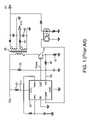
- the function of output power limitis generally used for the over-load and short circuit protection. Referring to FIG. 1 , a traditional switching power converter uses a control circuit 50 .
- the operation of the power converterstarts on the charging of a start-up capacitor 65 coupled to the supply terminal VCC of the control circuit 50 via a serial start-up resistor 30 for providing a supply voltage V CC by an input voltage V DC when the power is turned on until the supply voltage V CC is charged up to the threshold voltage, and then the output terminal OUT of the control circuit 50 starts to output a switching signal V PWM and drive the power converter.
- the supply voltage V CCis provided from the auxiliary bias winding of a transformer 20 through a rectifier 60 .
- a power transistor 10is coupled to the primary winding of the transformer 20 and the output terminal OUT.
- the power transistor 10switches the transformer 20 to control the output power of the power converter in response to the switching signal V PWM .
- a resistor 15 that is connected serially with the power transistor 10determines the maximum output power of the power converter.
- the methodis to connect a resistor 40 to the current-sense terminal VS of the control circuit 50 . If the voltage V S is greater than a maximum threshold, the control circuit 50 will disable the switching signal V PWM , and restrict the maximum output power of the power converter. However, the maximum output power is affected by a response time T D .
- the delay time T Dcauses a different over-power protection in response to the change of the input voltage V DC .
- a resistor 35is added between the input voltage V DC and the current-sense terminal VS for the feedforward compensation.
- the feedforward compensationis used to compensate the difference of the output power caused by the input voltage V DC and the delay time T D .
- present inventionuses a bleeding resistor for both start-up and feedforward compensation.
- the bleeding resistoris required to discharge EMI filter of the power converter for the safety purpose.
- the circuit of present inventionincludes an input terminal to connect the bleeding resistor for the start-up.
- a voltage divideris connected to the input terminal.
- a sample-and-hold circuitis further connected to the voltage divider to sample and hold a voltage signal from the voltage divider.
- a low-pass filteris utilized to filter out the line frequency ripple and generate an offset signal in accordance with the voltage signal.
- the low-pass filteris a sampling filter.
- the offset signalis connected to a limit circuit to generate a limit signal. The limit signal limits a switching current of the power converter.
- FIG. 1shows a circuit diagram of a prior art switching power converter
- FIG. 2shows a circuit diagram of a switching power converter in accordance with the present invention
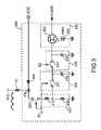
- FIG. 3shows a circuit diagram of a start up circuit with feedforward compensation in accordance with the present invention
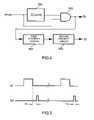
- FIG. 4shows a circuit diagram of a generating circuit for generating sample signals in accordance with the present invention.
- FIG. 5shows waveforms of the sample signals in accordance with the present invention.
- FIG. 2schematically shows a switching power converter according to the present invention.
- a control circuit 100comprises a start-up circuit 200 , a first comparator 110 , a second comparator 120 , a NAND gate 160 , a flip-flop 180 and an oscillator 150 , which serve to provide a pulse signal PLS for the flip-flop 180 .
- a bleeding resistor 70is required to discharge EMI filter of the power converter for the safety purpose. In order to save power and reduce device count, the present invention further uses the bleeding resistor 70 for both start-up and feedforward compensation.
- the bleeding resistor 70is connected between an input voltage V AC and an input terminal V IN of the control circuit 100 for the start-up.
- a bridge circuit 90is coupled between the input voltage V AC and the bleeding resistor 70 .
- the bridge circuit 90is further coupled to the primary winding of a transformer 25 .
- the input voltage V ACis applied to the start-up circuit 200 through the bleeding resistor 70 , and starts to charge up a start-up capacitor 69 for providing a supply voltage V CC to a supply terminal VCC of the control circuit 100 .
- the control circuit 100starts to operate and outputs a switching signal V PWM .
- the supply voltage V CCwill be provided from the auxiliary winding of the transformer 25 via a diode 67 .
- a limit signal V LIMIT of the start-up circuit 200is used to determine a maximum current-sense voltage, which is connected to the positive input terminal of the first comparator 110 .
- the positive input terminal of the second comparator 120is connected to a feedback terminal FB of the control circuit 100 for the output regulation of the power converter.
- An optical-coupler 55is coupled between the secondary winding of the transformer 25 and the feedback terminal FB to form a feedback control loop.
- the output voltage V O of the power converteris conducted to the optical-coupler 55 through a Zener diode 51 and a resistor 53 .
- the secondary winding of the transformer 25outputs the output voltage V O through a rectifier 57 .
- a filter capacitor 59is coupled to the rectifier 57 and the secondary winding.
- the negative input terminals of the first comparator 110 and second comparator 120are connected together to the source terminal of a power transistor 17 through a current-sense terminal VS of the control circuit 100 .
- the output terminals of the first comparator 110 and the second comparator 120are connected to the input terminals of the NAND gate 160 .
- the output terminal of the NAND gate 160is coupled to the reset terminal of the flip-flop 180 .
- the output terminal of the flip-flop 180is coupled to the gate terminal of the power transistor 17 and outputs the switching signal V PWM .
- the drain terminal of the power transistor 17is connected to the primary winding of the transformer 25 .
- a switching current I P flowing through a resistor 19produces a sense voltage V S in the resistor 19 .
- the first comparator 110will compare the sense voltage V S and the voltage of the limit signal V LIMIT . When the sense voltage V S is greater than the voltage of the limit signal V LIMIT , the first comparator 110 will output a logic low signal to the input terminal of the NAND gate 160 . Thus, the NAND gate 160 will output a logic high signal to the flip-flop 180 to reset the flip-flop 180 to disable the switching signal V PWM to turn off the power transistor 17 . Therefore, the output power limit is achieved.
- FIG. 3is a preferred embodiment of the start up circuit 200 .
- the input terminal V IN of the control circuit 100is connected to the input voltage V AC of the power converter via the bleeding resistor 70 .
- a diode 205is coupled from the input terminal V IN to the supply terminal VCC for providing power source to the control circuit 100 of the power converter.
- a voltage divider 207comprises resistors 210 and 220 . The resistor 210 and the resistor 220 are connected in series.
- the voltage divider 207is coupled to the input terminal V IN via a switch 225 .
- a sample-and-hold circuit 230is coupled to the voltage divider 207 to sample and hold a voltage signal from the voltage divider 207 .
- a low-pass filter 240is coupled to the sample-and-hold circuit 230 to generate an offset signal in accordance with the voltage signal.
- a limit circuit 250is coupled to the low-pass filter 240 for generating the limit signal V LIMIT in accordance with a reference signal 260 and the offset signal.
- the limit circuit 250comprises an adder 255 and the reference signal 260 .
- the reference signal 260is connected to the positive input terminal of the adder 255 .
- the offset signalis connected to the negative input terminal of the adder 255 . Therefore, the limit signal V LIMIT is decreased in response to the increase of the offset signal.
- the limit signal V LIMITis utilized to limit the switching current I P of the power converter. Accordingly, the feedforward compensation is achieved.
- the increase of the input voltage V ACwill reduce the switching current I P of the power converter. It is learned from above description that the present invention is a circuit with detection.
- the detectioncould be the line voltage detection.
- the sample-and-hold circuit 230comprises a first sample switch 231 and a first capacitor 235 .
- the first sample switch 231is connected to the voltage divider 207 .
- the first capacitor 235is connected to the first sample switch 231 to generate the voltage signal.
- the first sample switch 231is controlled by a first sample signal S 1 that is divided from the switching signal V PWM of the power converter.
- the first sample signal S 1also controls the switch 225 .
- the low pass filter 240comprises a second sample switch 241 and a second capacitor 245 .
- the second sample switch 241is connected to the first capacitor 235 of the sample-and-hold circuit 230 .
- the second capacitor 245is connected to the second sample switch 241 to generate the offset signal.
- the second sample switch 241is controlled by a second sample signal S 2 that is synchronized with the first sample signal S 1 . In order to accomplish the low pass filter the capacitance of the second capacitor 245 is higher than the capacitance of the first capacitor 235
- FIG. 4shows a circuit diagram of a generating circuit for generating the first sample signal S 1 and the second sample signal S 2 .
- the input terminal of a counter 300is connected to the output terminal of the flip-flop 180 to receive the switching signal V PWM .
- the output terminal of the counter 300is connected to the input terminal of an AND gate 310 .
- Another input terminal of the AND gate 310is connected to the output terminal of the flip-flop 180 to receive the switching signal V PWM .
- the output terminal of the AND gate 310generates the first sample signal S 1 .
- a first one-shot circuit 350is connected to receive the first sample signal S 1 .
- the output terminal of the first one-shot circuit 350is connected to the input terminal of a second one-shot circuit 360 .
- the second one-shot circuit 360generates the second sample signal S 2 .
- the first one-shot circuit 350determines a delay time T 1 in response to the falling edge of the first sample signal S 1 .
- the second one-shot circuit 360determines a pulse width T 2 for the second sample signal S 2 .
- FIG. 5shows waveforms of the sample signals S 1 and S 2 .
- the voltage of the limit signal V LIMITwill become a function of the input voltage V AC .
- the variation of the maximum switching current I pis inversely proportion to the deviation of the input voltage V AC .
- the low-pass filterfilters out the line frequency ripple of the input voltage V AC .
- the bleeding resistorcan therefore be used for the start-up, which further save the power. By properly select the resistance of the bleeding resistor can achieve an identical output power limit for the low line voltage and high line voltage input such as 90 Vac and 264 Vac.
Landscapes
- Engineering & Computer Science (AREA)
- Power Engineering (AREA)
- Dc-Dc Converters (AREA)
Abstract
Description
Claims (12)
Priority Applications (1)
| Application Number | Priority Date | Filing Date | Title |
|---|---|---|---|
| US11/406,309US7592790B2 (en) | 2006-04-19 | 2006-04-19 | Start-up circuit with feedforward compensation for power converters |
Applications Claiming Priority (1)
| Application Number | Priority Date | Filing Date | Title |
|---|---|---|---|
| US11/406,309US7592790B2 (en) | 2006-04-19 | 2006-04-19 | Start-up circuit with feedforward compensation for power converters |
Publications (2)
| Publication Number | Publication Date |
|---|---|
| US20070247879A1 US20070247879A1 (en) | 2007-10-25 |
| US7592790B2true US7592790B2 (en) | 2009-09-22 |
Family
ID=38619322
Family Applications (1)
| Application Number | Title | Priority Date | Filing Date |
|---|---|---|---|
| US11/406,309Active2026-10-28US7592790B2 (en) | 2006-04-19 | 2006-04-19 | Start-up circuit with feedforward compensation for power converters |
Country Status (1)
| Country | Link |
|---|---|
| US (1) | US7592790B2 (en) |
Cited By (10)
| Publication number | Priority date | Publication date | Assignee | Title |
|---|---|---|---|---|
| US20080310193A1 (en)* | 2007-06-14 | 2008-12-18 | Lin Chien Yuan | PWM Controller for Compensating a Maximum Output Power of a Power Converter |
| US20090185399A1 (en)* | 2008-01-22 | 2009-07-23 | Fun-Son Yeh | Active start judgment circuit |
| US20110062931A1 (en)* | 2009-09-17 | 2011-03-17 | Osamu Uehara | Dc-dc converter |
| US20120025793A1 (en)* | 2010-07-29 | 2012-02-02 | Richtek Technology Corp. | Offset and delay cancellation circuit for a switching dc-dc power supply |
| US20120176819A1 (en)* | 2011-01-10 | 2012-07-12 | Xiaolin Gao | Adaptively controlled soft start-up scheme for switching power converters |
| US8643297B2 (en) | 2011-03-22 | 2014-02-04 | System General Corporation | Control circuit and control method for dimming LED lighting circuit |
| US20140152283A1 (en)* | 2012-12-04 | 2014-06-05 | Chengdu Monolithic Power Systems Co., Ltd. | Voltage detecting circuit for switching converters and the method thereof |
| US9036383B2 (en) | 2012-09-19 | 2015-05-19 | Fuji Electric Co., Ltd. | Power supply device control circuit |
| US9240727B2 (en) | 2011-07-12 | 2016-01-19 | Fuji Electric Co., Ltd. | Switching power supply device control circuit having an overcurrent protection control circuit |
| CN106849636A (en)* | 2017-04-13 | 2017-06-13 | 四川长虹电器股份有限公司 | For the control circuit of Switching Power Supply |
Families Citing this family (24)
| Publication number | Priority date | Publication date | Assignee | Title |
|---|---|---|---|---|
| TWI353114B (en)* | 2008-09-22 | 2011-11-21 | Inventec Corp | Clock pin setting circuit and clock driven circuit |
| US8461915B2 (en)* | 2009-06-03 | 2013-06-11 | System General Corp. | Start-up circuit to discharge EMI filter for power saving of power supplies |
| TWI392186B (en)* | 2009-07-20 | 2013-04-01 | Apparatus and method for bleeding stored power | |
| US8115457B2 (en) | 2009-07-31 | 2012-02-14 | Power Integrations, Inc. | Method and apparatus for implementing a power converter input terminal voltage discharge circuit |
| US8471626B2 (en)* | 2009-08-12 | 2013-06-25 | System General Corp. | Start-up circuit to discharge EMI filter of power supplies |
| WO2011114828A1 (en)* | 2010-03-16 | 2011-09-22 | 株式会社村田製作所 | Driver circuit for power supply, integrated driver circuit for power supply, and power supply |
| US8698474B2 (en)* | 2010-06-11 | 2014-04-15 | System General Corp. | Start-up circuit with low standby power loss for power converters |
| JP5099183B2 (en)* | 2010-07-13 | 2012-12-12 | サンケン電気株式会社 | Start-up circuit |
| CN102377358B (en) | 2010-08-23 | 2014-09-10 | 昂宝电子(上海)有限公司 | System and method for reducing standby power consumption of power converter with switching mode |
| TWI419450B (en)* | 2010-09-20 | 2013-12-11 | 昂寶電子(上海)有限公司 | A system and method for reducing the standby power consumption of a switch mode power converter |
| US9374019B2 (en) | 2010-09-28 | 2016-06-21 | On-Bright Electronics (Shanghai) Co., Ltd. | Systems and methods for discharging an AC input capacitor with automatic detection |
| CN102075015B (en)* | 2011-01-19 | 2012-08-15 | 中国海洋石油总公司 | Towline high voltage direct current (DC) power supply for geophysical exploration |
| US8947895B2 (en)* | 2011-03-09 | 2015-02-03 | Marvell World Trade Ltd. | Two-peak current control for flyback voltage converters |
| EP2525492B1 (en)* | 2011-05-19 | 2019-07-10 | Nxp B.V. | Electronic switching device |
| CN102655378B (en)* | 2012-05-08 | 2014-06-04 | 成都芯源系统有限公司 | Isolated voltage converter circuit and control method thereof |
| US20130343090A1 (en)* | 2012-06-21 | 2013-12-26 | Fairchild Korea Semiconductor Ltd. | Active bleeder, active bleeding method, and power supply device where the active bleeder is applied |
| CN103580506B (en)* | 2012-07-19 | 2016-09-07 | 比亚迪股份有限公司 | Switching Power Supply and power supply control chip |
| US9025346B2 (en)* | 2012-09-12 | 2015-05-05 | Excelliance Mos Corporation | Fly-back power converting apparatus |
| US9112419B2 (en)* | 2013-07-16 | 2015-08-18 | Rohm Co., Ltd. | AC/DC converter with control circuit that receives rectified voltage at input detection terminal |
| TWI503702B (en)* | 2013-12-17 | 2015-10-11 | Univ Chaoyang Technology | Olfaction feedback apparatus for virtual reality system |
| US9712045B2 (en)* | 2014-11-17 | 2017-07-18 | Infineon Technologies Austria Ag | System and method for a startup cell circuit |
| KR102107883B1 (en)* | 2017-12-21 | 2020-05-08 | 매그나칩 반도체 유한회사 | High voltage start-up circuit for zeroing of standby power consumption and switching mode power supply having the same |
| TWI721593B (en)* | 2019-10-09 | 2021-03-11 | 產晶積體電路股份有限公司 | Power detection power controller |
| TWI737292B (en)* | 2020-05-08 | 2021-08-21 | 通嘉科技股份有限公司 | Voltage mode controller applied to short-circuited protection of a power converter and operational method thereof |
Citations (4)
| Publication number | Priority date | Publication date | Assignee | Title |
|---|---|---|---|---|
| US4879478A (en)* | 1985-08-30 | 1989-11-07 | Advanced Micro Devices, Inc. | Fast sample and hold circuit |
| US5721480A (en)* | 1996-01-31 | 1998-02-24 | Kabushiki Kaisha Toshiba | System and method for controlling charging of secondary battery that requires constant-voltage charge control |
| US5790526A (en)* | 1991-04-29 | 1998-08-04 | Philips Electronics North America Corporation | Bi-directional signal transmission system and adapter for such a system |
| US6501255B2 (en)* | 2000-11-21 | 2002-12-31 | Lake Shore Cryotronics, Inc. | Differential current source with active common mode reduction |
Family Cites Families (6)
| Publication number | Priority date | Publication date | Assignee | Title |
|---|---|---|---|---|
| US2927023A (en)* | 1956-08-27 | 1960-03-01 | Du Pont | Photopolymerizable compositions |
| BE599102A (en)* | 1960-01-27 | |||
| US3469983A (en)* | 1965-07-06 | 1969-09-30 | Gaf Corp | Preparation of photopolymer lithographic offset paper plates |
| US3898087A (en)* | 1974-06-14 | 1975-08-05 | Ball Corp | Photopolymerizable compositions containing aminimides |
| US4221859A (en)* | 1976-05-04 | 1980-09-09 | Ball Corporation | Photopolymerizable composition with oxalic acid photoinitiator |
| GB2108986B (en)* | 1981-11-03 | 1985-06-26 | Sericol Group Ltd | Photopolymerisable composition for producing screen printing stencils |
- 2006
- 2006-04-19USUS11/406,309patent/US7592790B2/enactiveActive
Patent Citations (4)
| Publication number | Priority date | Publication date | Assignee | Title |
|---|---|---|---|---|
| US4879478A (en)* | 1985-08-30 | 1989-11-07 | Advanced Micro Devices, Inc. | Fast sample and hold circuit |
| US5790526A (en)* | 1991-04-29 | 1998-08-04 | Philips Electronics North America Corporation | Bi-directional signal transmission system and adapter for such a system |
| US5721480A (en)* | 1996-01-31 | 1998-02-24 | Kabushiki Kaisha Toshiba | System and method for controlling charging of secondary battery that requires constant-voltage charge control |
| US6501255B2 (en)* | 2000-11-21 | 2002-12-31 | Lake Shore Cryotronics, Inc. | Differential current source with active common mode reduction |
Cited By (16)
| Publication number | Priority date | Publication date | Assignee | Title |
|---|---|---|---|---|
| US20080310193A1 (en)* | 2007-06-14 | 2008-12-18 | Lin Chien Yuan | PWM Controller for Compensating a Maximum Output Power of a Power Converter |
| US8031492B2 (en)* | 2007-06-14 | 2011-10-04 | System General Corp. | PWM controller for compensating a maximum output power of a power converter |
| US20090185399A1 (en)* | 2008-01-22 | 2009-07-23 | Fun-Son Yeh | Active start judgment circuit |
| US7719863B2 (en)* | 2008-01-22 | 2010-05-18 | Shuttle, Inc. | Active start judgment circuit |
| US20110062931A1 (en)* | 2009-09-17 | 2011-03-17 | Osamu Uehara | Dc-dc converter |
| US8416591B2 (en)* | 2009-09-17 | 2013-04-09 | Seiko Instruments Inc. | DC-DC converter with soft start circuit |
| US20120025793A1 (en)* | 2010-07-29 | 2012-02-02 | Richtek Technology Corp. | Offset and delay cancellation circuit for a switching dc-dc power supply |
| US8791678B2 (en)* | 2010-07-29 | 2014-07-29 | Richtek Technology Corp. | Offset and delay cancellation circuit for a switching DC-DC power supply |
| US8582329B2 (en)* | 2011-01-10 | 2013-11-12 | Iwatt Inc. | Adaptively controlled soft start-up scheme for switching power converters |
| US20120176819A1 (en)* | 2011-01-10 | 2012-07-12 | Xiaolin Gao | Adaptively controlled soft start-up scheme for switching power converters |
| US8643297B2 (en) | 2011-03-22 | 2014-02-04 | System General Corporation | Control circuit and control method for dimming LED lighting circuit |
| US9240727B2 (en) | 2011-07-12 | 2016-01-19 | Fuji Electric Co., Ltd. | Switching power supply device control circuit having an overcurrent protection control circuit |
| US9036383B2 (en) | 2012-09-19 | 2015-05-19 | Fuji Electric Co., Ltd. | Power supply device control circuit |
| US20140152283A1 (en)* | 2012-12-04 | 2014-06-05 | Chengdu Monolithic Power Systems Co., Ltd. | Voltage detecting circuit for switching converters and the method thereof |
| US9431913B2 (en)* | 2012-12-04 | 2016-08-30 | Chengdu Monolithic Power Systems Co., Ltd. | Voltage detecting circuit for switching converters and the method thereof |
| CN106849636A (en)* | 2017-04-13 | 2017-06-13 | 四川长虹电器股份有限公司 | For the control circuit of Switching Power Supply |
Also Published As
| Publication number | Publication date |
|---|---|
| US20070247879A1 (en) | 2007-10-25 |
Similar Documents
| Publication | Publication Date | Title |
|---|---|---|
| US7592790B2 (en) | Start-up circuit with feedforward compensation for power converters | |
| CN108880296B (en) | power conversion system | |
| US10461649B2 (en) | Switched-mode power supply circuit | |
| TWI599160B (en) | Flyback power converter and controller and driver thereof | |
| US8698474B2 (en) | Start-up circuit with low standby power loss for power converters | |
| US9948187B2 (en) | System and method for a switched-mode power supply | |
| US6788557B2 (en) | Single conversion power converter with hold-up time | |
| US6429709B1 (en) | Power converter circuit and method for controlling | |
| US10199942B2 (en) | Controller and power supply | |
| US10020744B2 (en) | Circuits and methods for reducing output voltage overshoot of switch mode power supply | |
| TWI589106B (en) | Switching power supplies and switch controllers | |
| US20210119526A1 (en) | Partial zero voltage switching (zvs) for flyback power converter and method therefor | |
| US20060274468A1 (en) | Active inrush current control using a relay for AC to DC converters | |
| US8737091B2 (en) | Variable time clamp for a power supply controller | |
| JP5910395B2 (en) | Drive circuit | |
| CN110932553B (en) | Power supply control apparatus | |
| CN212486401U (en) | Power supply and peripheral circuits for power supply | |
| TWI672894B (en) | Power controllers and control methods thereof | |
| US20200195128A1 (en) | Power supply device, power supply control device, and power supply control method | |
| WO2008071094A1 (en) | Method and circuit for providing compensations of current mode power converters | |
| US8749999B2 (en) | Controller and power converter using the same for clamping maximum switching current of power converter | |
| CN112994463A (en) | Switch control circuit and power supply circuit | |
| CN100525025C (en) | Start-up circuit with feedforward compensation for power converter | |
| CN113726176B (en) | Conversion circuit with delay high-voltage power supply, controller and delay high-voltage power supply method thereof | |
| US20240258911A1 (en) | Controller for resonant power converter, resonant power converter and method of operating a resonant power converter |
Legal Events
| Date | Code | Title | Description |
|---|---|---|---|
| AS | Assignment | Owner name:SYSTEM GENERAL CORP., TAIWAN Free format text:ASSIGNMENT OF ASSIGNORS INTEREST;ASSIGNOR:YANG, TA-YUNG;REEL/FRAME:017528/0263 Effective date:20060412 | |
| STCF | Information on status: patent grant | Free format text:PATENTED CASE | |
| FPAY | Fee payment | Year of fee payment:4 | |
| AS | Assignment | Owner name:FAIRCHILD (TAIWAN) CORPORATION, TAIWAN Free format text:CHANGE OF NAME;ASSIGNOR:SYSTEM GENERAL CORP.;REEL/FRAME:038906/0030 Effective date:20140620 | |
| FPAY | Fee payment | Year of fee payment:8 | |
| AS | Assignment | Owner name:SEMICONDUCTOR COMPONENTS INDUSTRIES, LLC, ARIZONA Free format text:ASSIGNMENT OF ASSIGNORS INTEREST;ASSIGNOR:FAIRCHILD (TAIWAN) CORPORATION (FORMERLY SYSTEM GENERAL CORPORATION);REEL/FRAME:042328/0318 Effective date:20161221 | |
| AS | Assignment | Owner name:DEUTSCHE BANK AG NEW YORK BRANCH, AS COLLATERAL AGENT, NEW YORK Free format text:PATENT SECURITY AGREEMENT;ASSIGNOR:SEMICONDUCTOR COMPONENTS INDUSTRIES, LLC;REEL/FRAME:046410/0933 Effective date:20170210 Owner name:DEUTSCHE BANK AG NEW YORK BRANCH, AS COLLATERAL AG Free format text:PATENT SECURITY AGREEMENT;ASSIGNOR:SEMICONDUCTOR COMPONENTS INDUSTRIES, LLC;REEL/FRAME:046410/0933 Effective date:20170210 | |
| MAFP | Maintenance fee payment | Free format text:PAYMENT OF MAINTENANCE FEE, 12TH YEAR, LARGE ENTITY (ORIGINAL EVENT CODE: M1553); ENTITY STATUS OF PATENT OWNER: LARGE ENTITY Year of fee payment:12 | |
| AS | Assignment | Owner name:FAIRCHILD SEMICONDUCTOR CORPORATION, ARIZONA Free format text:RELEASE OF SECURITY INTEREST IN PATENTS RECORDED AT RECORDED AT REEL 046410, FRAME 0933;ASSIGNOR:DEUTSCHE BANK AG NEW YORK BRANCH, AS COLLATERAL AGENT;REEL/FRAME:064072/0001 Effective date:20230622 Owner name:SEMICONDUCTOR COMPONENTS INDUSTRIES, LLC, ARIZONA Free format text:RELEASE OF SECURITY INTEREST IN PATENTS RECORDED AT RECORDED AT REEL 046410, FRAME 0933;ASSIGNOR:DEUTSCHE BANK AG NEW YORK BRANCH, AS COLLATERAL AGENT;REEL/FRAME:064072/0001 Effective date:20230622 |