US7591780B2 - Miniaturized imaging device with integrated circuit connector system - Google Patents
Miniaturized imaging device with integrated circuit connector systemDownload PDFInfo
- Publication number
- US7591780B2 US7591780B2US10/391,513US39151303AUS7591780B2US 7591780 B2US7591780 B2US 7591780B2US 39151303 AUS39151303 AUS 39151303AUS 7591780 B2US7591780 B2US 7591780B2
- Authority
- US
- United States
- Prior art keywords
- ssid
- conductive wires
- imaging device
- conductive
- lens
- Prior art date
- Legal status (The legal status is an assumption and is not a legal conclusion. Google has not performed a legal analysis and makes no representation as to the accuracy of the status listed.)
- Expired - Lifetime
Links
- 238000003384imaging methodMethods0.000titleclaimsabstractdescription128
- 238000000060site-specific infrared dichroism spectroscopyMethods0.000claimsabstractdescription120
- 230000003287optical effectEffects0.000claimsdescription16
- 238000000034methodMethods0.000abstractdescription16
- 238000004891communicationMethods0.000abstractdescription9
- 239000000463materialSubstances0.000description63
- 239000000758substrateSubstances0.000description45
- 239000004020conductorSubstances0.000description32
- 229920002120photoresistant polymerPolymers0.000description27
- 239000002184metalSubstances0.000description12
- 229910052751metalInorganic materials0.000description12
- 230000037361pathwayEffects0.000description12
- 210000003484anatomyAnatomy0.000description11
- 239000012530fluidSubstances0.000description11
- 239000004593EpoxySubstances0.000description10
- 239000000835fiberSubstances0.000description10
- VYPSYNLAJGMNEJ-UHFFFAOYSA-NSilicium dioxideChemical compoundO=[Si]=OVYPSYNLAJGMNEJ-UHFFFAOYSA-N0.000description8
- 230000008878couplingEffects0.000description8
- 238000010168coupling processMethods0.000description8
- 238000005859coupling reactionMethods0.000description8
- 238000004519manufacturing processMethods0.000description8
- 239000000853adhesiveSubstances0.000description7
- 230000001070adhesive effectEffects0.000description7
- 239000007787solidSubstances0.000description7
- 238000002059diagnostic imagingMethods0.000description6
- 230000006870functionEffects0.000description6
- 239000012811non-conductive materialSubstances0.000description6
- 229920000642polymerPolymers0.000description6
- 230000000007visual effectEffects0.000description6
- XUIMIQQOPSSXEZ-UHFFFAOYSA-NSiliconChemical compound[Si]XUIMIQQOPSSXEZ-UHFFFAOYSA-N0.000description5
- 230000008901benefitEffects0.000description5
- 239000011248coating agentSubstances0.000description5
- 238000000576coating methodMethods0.000description5
- 229910052710siliconInorganic materials0.000description5
- 239000010703siliconSubstances0.000description5
- 230000009977dual effectEffects0.000description4
- 235000012239silicon dioxideNutrition0.000description4
- 239000000377silicon dioxideSubstances0.000description4
- KRHYYFGTRYWZRS-UHFFFAOYSA-NFluoraneChemical compoundFKRHYYFGTRYWZRS-UHFFFAOYSA-N0.000description3
- 210000001124body fluidAnatomy0.000description3
- 239000010839body fluidSubstances0.000description3
- 239000003086colorantSubstances0.000description3
- 238000012377drug deliveryMethods0.000description3
- 238000005516engineering processMethods0.000description3
- PCHJSUWPFVWCPO-UHFFFAOYSA-NgoldChemical compound[Au]PCHJSUWPFVWCPO-UHFFFAOYSA-N0.000description3
- 239000010931goldSubstances0.000description3
- 229910052737goldInorganic materials0.000description3
- 238000003973irrigationMethods0.000description3
- 230000002262irrigationEffects0.000description3
- 238000003754machiningMethods0.000description3
- 238000012986modificationMethods0.000description3
- 230000004048modificationEffects0.000description3
- 230000008569processEffects0.000description3
- 230000005855radiationEffects0.000description3
- 229910000679solderInorganic materials0.000description3
- 230000000153supplemental effectEffects0.000description3
- 238000007514turningMethods0.000description3
- CSCPPACGZOOCGX-UHFFFAOYSA-NAcetoneChemical compoundCC(C)=OCSCPPACGZOOCGX-UHFFFAOYSA-N0.000description2
- FAPWRFPIFSIZLT-UHFFFAOYSA-MSodium chlorideChemical compound[Na+].[Cl-]FAPWRFPIFSIZLT-UHFFFAOYSA-M0.000description2
- 229910021417amorphous siliconInorganic materials0.000description2
- 239000000919ceramicSubstances0.000description2
- 238000010276constructionMethods0.000description2
- 239000013078crystalSubstances0.000description2
- 238000013461designMethods0.000description2
- 238000009792diffusion processMethods0.000description2
- 238000005530etchingMethods0.000description2
- 230000005496eutecticsEffects0.000description2
- 208000014674injuryDiseases0.000description2
- 239000012212insulatorSubstances0.000description2
- 230000000873masking effectEffects0.000description2
- 229920003229poly(methyl methacrylate)Polymers0.000description2
- 239000004926polymethyl methacrylateSubstances0.000description2
- 229910052709silverInorganic materials0.000description2
- 239000004332silverSubstances0.000description2
- 239000002904solventSubstances0.000description2
- 239000000126substanceSubstances0.000description2
- 239000010409thin filmSubstances0.000description2
- 238000012546transferMethods0.000description2
- 230000008733traumaEffects0.000description2
- 238000012935AveragingMethods0.000description1
- 239000006090FoturanSubstances0.000description1
- 241000282412HomoSpecies0.000description1
- 230000004075alterationEffects0.000description1
- 238000004458analytical methodMethods0.000description1
- 238000003491arrayMethods0.000description1
- 238000005452bendingMethods0.000description1
- 230000005540biological transmissionEffects0.000description1
- 210000001072colonAnatomy0.000description1
- 230000000295complement effectEffects0.000description1
- 238000013500data storageMethods0.000description1
- 230000008021depositionEffects0.000description1
- 238000005553drillingMethods0.000description1
- 239000003814drugSubstances0.000description1
- 238000001312dry etchingMethods0.000description1
- 238000009713electroplatingMethods0.000description1
- 239000003974emollient agentSubstances0.000description1
- 210000003238esophagusAnatomy0.000description1
- 230000008020evaporationEffects0.000description1
- 238000001704evaporationMethods0.000description1
- 238000011049fillingMethods0.000description1
- 238000000227grindingMethods0.000description1
- 210000002216heartAnatomy0.000description1
- 238000011065in-situ storageMethods0.000description1
- 238000002347injectionMethods0.000description1
- 239000007924injectionSubstances0.000description1
- 230000002452interceptive effectEffects0.000description1
- 150000002500ionsChemical class0.000description1
- 238000001459lithographyMethods0.000description1
- 210000004072lungAnatomy0.000description1
- 229910044991metal oxideInorganic materials0.000description1
- 150000004706metal oxidesChemical class0.000description1
- 150000002739metalsChemical class0.000description1
- 238000005459micromachiningMethods0.000description1
- 238000012544monitoring processMethods0.000description1
- QPJSUIGXIBEQAC-UHFFFAOYSA-Nn-(2,4-dichloro-5-propan-2-yloxyphenyl)acetamideChemical compoundCC(C)OC1=CC(NC(C)=O)=C(Cl)C=C1ClQPJSUIGXIBEQAC-UHFFFAOYSA-N0.000description1
- 210000003101oviductAnatomy0.000description1
- 239000006089photosensitive glassSubstances0.000description1
- 239000002861polymer materialSubstances0.000description1
- 238000003825pressingMethods0.000description1
- 238000012545processingMethods0.000description1
- 239000011347resinSubstances0.000description1
- 229920005989resinPolymers0.000description1
- 238000005070samplingMethods0.000description1
- 239000004065semiconductorSubstances0.000description1
- 239000011780sodium chlorideSubstances0.000description1
- 238000005476solderingMethods0.000description1
- 230000006641stabilisationEffects0.000description1
- 238000011105stabilizationMethods0.000description1
- 210000002784stomachAnatomy0.000description1
- 238000001356surgical procedureMethods0.000description1
- 235000013619trace mineralNutrition0.000description1
- 239000011573trace mineralSubstances0.000description1
- 238000012795verificationMethods0.000description1
- 230000001720vestibularEffects0.000description1
- 238000011179visual inspectionMethods0.000description1
- 238000003466weldingMethods0.000description1
- 238000001039wet etchingMethods0.000description1
Images


Classifications
- A—HUMAN NECESSITIES
- A61—MEDICAL OR VETERINARY SCIENCE; HYGIENE
- A61B—DIAGNOSIS; SURGERY; IDENTIFICATION
- A61B1/00—Instruments for performing medical examinations of the interior of cavities or tubes of the body by visual or photographical inspection, e.g. endoscopes; Illuminating arrangements therefor
- A61B1/04—Instruments for performing medical examinations of the interior of cavities or tubes of the body by visual or photographical inspection, e.g. endoscopes; Illuminating arrangements therefor combined with photographic or television appliances
- A61B1/05—Instruments for performing medical examinations of the interior of cavities or tubes of the body by visual or photographical inspection, e.g. endoscopes; Illuminating arrangements therefor combined with photographic or television appliances characterised by the image sensor, e.g. camera, being in the distal end portion
- H—ELECTRICITY
- H04—ELECTRIC COMMUNICATION TECHNIQUE
- H04N—PICTORIAL COMMUNICATION, e.g. TELEVISION
- H04N23/00—Cameras or camera modules comprising electronic image sensors; Control thereof
- H04N23/50—Constructional details
- H04N23/555—Constructional details for picking-up images in sites, inaccessible due to their dimensions or hazardous conditions, e.g. endoscopes or borescopes
Definitions
- the inventionrelates generally to solid state imaging devices (SSIDs). More specifically, the invention relates to miniaturized imaging devices that are particularly suited to viewing beyond small openings and traversing small-diameter areas. These devices can be used for catheter-borne medical imaging within the anatomy of a patient, and are useful for other applications.
- SSIDssolid state imaging devices
- Small imaging devicesthat take advantage of advances in integrated circuit imaging technologies are known. Such small imaging devices can be particularly useful in medical diagnostic and treatment applications. Portions of human anatomy previously viewable only by a surgical procedure can be viewed now by a minimally invasive catheterization, provided an imaging device can be made that is small enough to view the target anatomy.
- imaging devicescan be used and are desirable for surveillance applications, for monitoring of conditions and functions within devices, and for size- and weight-critical imaging needs as are present in aerospace applications, to name a few.
- the medical imaging applicationcan be used to favorably illustrate unique advantages of the invention.
- the desirability of providing imaging at sites within the anatomy of living creatures, especially humans, distal of a small orifice or luminal spacehas long been recognized.
- a wide variety of types and sub-types of endoscopeshave been developed for this purpose.
- CIDcharge-injection device
- CCDcharge-coupled device
- CMOScomplementary metal oxide semiconductor
- the inventionaccordingly provides a miniaturized imaging device, comprising a lens, an SSID, an umbilical, and an adaptor.
- the lenscan be a GRIN lens, or another type of lens, including a wide angle lens or prism lens.
- the SSIDcan include an imaging array optically coupled to the lens.
- the umbilicalcan include a conductive line, such as a plurality of conductive wires to provide power, ground, clock signal, and output signal.
- the conductive linecan include at least two conductive wires that are electrically isolated from one another.
- the adaptorcan be configured to support the lens and provide electrical communication between the SSID and conductive line.
- a miniaturized imaging devicecan comprise a lens, an SSID including an imaging array optically coupled to the lens, an umbilical including a conductive line, and a rigid adaptor.
- the rigid adaptorcan be configured to provide electrical communication between the SSID and the conductive line through a conductive path.
- the conductive pathcan be configured along multiple contiguous surfaces of the adaptor such that the SSID is electrically coupled to the conductive path at a first surface, and the conductive line is electrically coupled to the conductive path at a non-coplanar second surface.
- the adaptorcan be configured to have a side surface and an adjacent bottom surface, wherein a conductive strip is present that has electrically continuous properties from the side surface to the bottom surface.
- the conductive line of the umbilicalsuch as electrical wires, can be configured to electrically contact one or more conductive strip at the side surface of the adaptor.
- the SSIDcan electrically contact the conductive strip(s) at the bottom surface of the adaptor.
- the conductive linecan be placed in electrical communication with the SSID through the adaptor.
- Other configurationsare also available, as will be described by example hereinafter.
- the adaptorcan be configured such that multiple separate electrical signals, e.g., four, can pass therethrough at the same time without the signals substantially interfering with one another.
- the adaptorcan be smaller than 500 microns in length, width, and height, respectively.
- the SSIDtypically includes an imaging array, and can further include conductive pads electrically coupled to the imaging array.
- the conductive padscan provide electrical communication between the SSID and the conductive line through the adaptor.
- the SSIDcan be one of many known SSIDs, including a CCD, a CID, or a CMOS imaging device.
- the optical coupling of the lens and the imaging array of the SSIDcan be direct, or can be through an optical intermediate device, such as a color filter insert, a fiber optic, a prism, or a wide angle lens, for example.
- a color filter insertis described herein in detail.
- a color filter insertcan be used for producing multiple colors from a monochromatic camera image.
- An example of such a color filter insertincludes a filter configured in a Bayer filter pattern.
- a utility guidecan also optionally be present.
- a utility guidecan be configured for carrying utilities to the SSID, adaptor, or lens.
- a utility that can be presentincludes a light source carried by the SSID, the adaptor, and/or the utility guide.
- Alternative or additional utilities that can be presentinclude electrical wires, temperature sensors, force sensors, fluid irrigation or aspiration members, pressure sensors, fiber optics, microforceps, material retrieval tools, drug delivery devices, radiation emitting devices, laser diodes, electric cauterizers, and electric stimulators. These utilities can be carried to a distal tip of the device via the umbilical.
- a method of operating a microcameracan comprise the steps of (a) optically coupling a lens to an imaging array of an SSID, wherein the SSID is electrically coupled to a rigid adaptor; (b) defining a plurality of conductive paths, wherein at least one of the conductive paths is configured along multiple non-coplanar surfaces of the adaptor; (c) powering the SSID through a first of the conductive paths; and (d) receiving signal from the SSID through a second of the conductive paths.
- the adaptorcan be configured to support the lens as well.
- the methodcan further comprise the step of illuminating an area around the lens, such that light or photon energy can be received by an imaging array of the SSID.
- the step of optically coupling the lens to the SSIDcan be by directly attaching the lens to an imaging array of the SSID, such as by an optically clear epoxy substance.
- the step of optically coupling the lens to the SSIDcan be by interposing an intermediate optical device between the lens and an imaging array of the SSID.
- the step of defining a plurality of conductive pathsincludes defining at least four conductive paths.
- groundcan be provided to the SSID through a third conductive path
- controlcan be provided to the SSID through a fourth conductive path.
- a method of making an adaptor or connector block in accordance with an embodiment of the present inventionincludes the steps of (a) applying a conductive material layer to an adaptor substrate; (b) applying a photoresist material layer to the conductive material layer; (c) developing a portion of the photoresist material layer, such that a first portion of the conductive material layer is exposed, and a second portion of the conductive material layer is protected; and (d) removing the first portion of the conductive material from the adaptor substrate.
- Other stepscan include the preliminary steps of applying a removable layer to a working substrate, followed by applying the adaptor substrate to the removable layer. Additionally, a step of removing the adaptor substrate from the removable layer after the first portion of the conductive material is removed from the adaptor substrate can also be carried out.
- the step of developing a portion of the photoresist materialcan be by applying heat from beneath the working substrate, and/or applying UV light to a portion of the photoresist material that protects the first portion of the conductive material. This selective application of UV light can be accomplished by using a photomask.
- the photoresist materialis completely removed after the first portion of the conductive material is removed from the adaptor substrate. If the adaptor is used for embodiments wherein a lens is supported by the adaptor, the step of drilling a hole through the adaptor substrate to configure the adaptor to also support a lens can be carried out. With respect to these adaptors, typically, the adaptor is less than 500 microns in length, width, and height, respectively.
- FIG. 1is a schematic illustration of an exemplary medical imaging system in accordance with principles of the invention
- FIG. 2is a side view of an exemplary embodiment of the present invention, which is an enlarged view of device 14 of FIG. 1 ;
- FIG. 3is a perspective exploded view of another exemplary embodiment of the invention.
- FIG. 4is a schematic perspective illustration of a conventional wire bonding connection system consistent with the prior art
- FIG. 5is an exploded schematic perspective illustration of an embodiment of the connector system in accordance with the present invention.
- FIG. 6is a schematic perspective illustration of an embodiment of the connector system in accordance with the present invention, wherein the SSID is movable for viewing various angles with respect to the umbilical;
- FIG. 7is a perspective view of an adaptor incorporating conductive pathways in one embodiment
- FIG. 8is a schematic side view illustration of a connection between two chips, such as SSIDs, including the adaptor of FIG. 7 ;
- FIG. 9is a perspective view of an adaptor incorporating conductive pathways in another embodiment
- FIG. 10is a schematic side view illustration of a connection between two chips, such as SSIDs, including the adaptor of FIG. 9 ;
- FIG. 11is a schematic perspective illustration of a fabrication technique for modifying a connector body to form a pathway through an interior portion, thereby forming an adaptor, the adaptor being not yet cut free, but shown in outline form within a larger preform block of material;
- FIG. 12is a side crossectional view of a connector body as shown in FIG. 11 taken along line 2 - 2 ;
- FIG. 13is a schematic perspective illustration of another fabrication technique for forming an adaptor having conductive pathway(s) through an interior portion thereof, showing a preform block constructed in accordance with one embodiment, the connector body to be formed therefrom being shown in outline;
- FIG. 14is a perspective view of a connector body of FIG. 13 after machining from the block;
- FIG. 15is a perspective exploded view of another exemplary embodiment of the invention, wherein connector block also supports the lens;
- FIG. 16is a cross sectional exploded side view of the exemplary embodiment of FIG. 15 ;
- FIG. 17is a perspective exploded view of another exemplary embodiment of the invention.
- FIG. 18is a perspective assembled view of the exemplary embodiment of FIG. 17 ;
- FIG. 19is a cross sectional view of another exemplary embodiment of the invention.
- FIG. 20is a perspective view of an adaptor or connector block of FIG. 19 ;
- FIGS. 21 a to 21 hprovide cross-sectional representations of two adaptors at various preparative stages
- FIG. 22is plan view along the optical axis of an exemplary color filter insert that can be used with imaging devices in accordance with principles of the invention.
- FIG. 23is a side view of the color filter insert of FIG. 22 ;
- FIG. 24is a second side view of the color filter insert of FIG. 22 , taken at 90 degrees with respect to FIG. 23 ;
- FIG. 25is a schematic cross sectional representation of an example of a device similar to that shown in FIG. 19 , having a color filter insert of FIG. 22 inserted therein;
- FIG. 26is a bottom perspective view of an exemplary adaptor or connector block integrated with a color filter insert.
- FIG. 27is a top perspective view of an exemplary adaptor or connector block integrated with a color filter insert.
- An “SSID,” “solid state imaging device,” or “SSID chip” in the exemplary embodimentsgenerally comprises a substrate carrying an imaging array or pixel array for gathering image data, and can further comprise conductive pads electrically coupled to the imaging array, which facilitates electrical communication therebetween.
- the SSIDcan comprise a silicon or silicon-like substrate or amorphous silicon thin film transistors (TFT) having features typically manufactured therein.
- TFTthin film transistors
- Featurescan include the imaging array, the conductive pads, metal traces, circuitry, etc.
- Other integrated circuit componentscan also be present for desired applications. However, it is not required that all of these components be present, as long as there is a means of gathering visual or photon data, and a means of sending that data to provide a visual image or image reconstruction.
- an umbilicalcan include the collection of utilities that operate the SSID or the micro-camera as a whole.
- an umbilicalincludes a conductive line, such as electrical wire(s), for providing power, ground, clock signal, and output signal with respect to the SSID, though not all of these are strictly required.
- groundcan be provide by another means than through an umbilical wire, e.g., to a camera housing, etc.
- the umbilicalcan also include other utilities such as a light source, temperature sensors, force sensors, fluid irrigation or aspiration members, pressure sensors, fiber optics, microforceps, material retrieval tools, drug delivery devices, radiation emitting devices, laser diodes, electric cauterizers, and electric stimulators, for example.
- Other utilitieswill also be apparent to those skilled in the art and are thus comprehended by this disclosure.
- GRIN lensor “graduated refractive index lens” refers to a specialized lens that has a refractive index that is varied radially from a center optical axis to the outer diameter of the lens.
- such a lenscan be configured in a cylindrical shape, with the optical axis extending from a first flat end to a second flat end.
- a lens of this shapecan simulate the affects of a more traditionally shaped lens.
- a GRIN lensis often used to exemplify an embodiment of the invention, the use of such a lens is not required.
- Other lensescan also be used as are known by those skilled in the art.
- Adaptor“connector block,” or “integrated circuit connector system” refers to a rigid device that can provide a solid electrical connection between a conductive line of an umbilical and conductive pads of an SSID.
- the adaptor or connector blockcan function to support the lens as well.
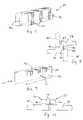
- the inventionis embodied in a medical imaging system 10 , including a catheter 12 having an imaging capability by means of an imaging device, shown generally at 14 , at a distal tip 15 of the catheter.
- the systemfurther includes a fitting 16 enabling an imaging fluid, such as a clear saline solution, to be dispensed to the distal tip portion of the catheter from a reservoir 18 to displace body fluids as needed to provide a clearer image.
- a pump 20is provided, and is manually actuated by a medical practitioner performing a medical imaging procedure, or can be automated and electronically controlled so as to dispense fluid on demand according to control signals from the practitioner, sensors, or according to software commands.
- a processor 22such as an appropriately programmed computer, is provided to control the imaging system 10 and create an image of anatomy adjacent the distal tip portion 15 , within a patient (not shown), displayable on a monitor 24 , and storable in a data storage device 26 .
- An interface 28is provided which supplies power to the imaging device 14 and feeds a digital image signal to the processor based on a signal received from the imaging device via an electrical umbilical 30 , including conductive wires 32 , a fluid dispenser 34 , and a light source 44 , through the catheter 12 .
- the interfacecan also be configured to control the pump 20 based on control signals from the processor or a medical practitioner performing an imaging procedure.
- the imaging device 14 at the distal tip 15can include a utility guide 36 for supporting or carrying the umbilical 30 , which can include electrical wires 32 , a fluid dispenser 34 , and a light source 44 .
- Other components that can be carried by the utility guidecan include, temperature sensors, force sensors, fluid irrigation or aspiration members, pressure sensors, fiber optics, microforceps, material retrieval tools, drug delivery devices, radiation emitting devices, laser diodes, electric cauterizers, and electric stimulators.
- the utility guidecan also carry an SSID or solid state imaging device 38 that includes an imaging array (not shown) and conductive pads 42 for coupling the electrical wires to the SSID.
- the SSID 38is electrically bonded to electrical or conductive wires 32 through an adaptor 52 .
- the adaptorprovides the dual function of supporting a lens 40 (which in this embodiment, is a GRIN lens), and innervating the SSID via the umbilical. More specifically, power, signal, and control commands are carried to and from the SSID through metal traces or conductive strips 56 that extend from a side surface to a bottom surface of the adaptor.
- the light source 44 shownis a fiber optic carried by the utility guide 36 .
- other light sourcescan be used, such as those carried by the SSID 38 or adaptor 52 .
- the SSID or adaptorcan include light-emitting diodes (LEDs) configured to illuminate the area immediately adjacent the distal tip portion.
- LEDslight-emitting diodes
- the lens 40can be a GRIN lens that is substantially cylindrical in shape, which is optically coupled to the imaging array of the SSID 38 .
- the GRIN lenscan have a first flat end for receiving light, a second flat end for passing the light to the imaging array, and an outer curved surface surrounded by an opaque coating or sleeve member to prevent unwanted light from entering the GRIN lens.
- the GRIN lenscan be optically coupled to the imaging array by direct contact between the second flat end and the imaging array of the SSID. Such direct contact can include an optically transparent or translucent bonding material at the interface between the second flat end and the imaging array.
- the GRIN lenscan be optically coupled to the imaging array of the SSID through an intermediate optical device, such as a fiber optic or a color filter, or any shape optical lens such as a prism or wide angle lens.
- an intermediate optical devicesuch as a fiber optic or a color filter, or any shape optical lens such as a prism or wide angle lens.
- a GRIN lensis shown in this embodiment, other lenses that can be optically coupled to an SSID 38 can be used, as will be exemplified hereinafter.
- the catheter 12can be configured to be bendable and flexible so as to be steerable within a patient's anatomy and to minimize trauma.
- the cathetercan comprise a micromachined tube 46 at the distal tip portion, and cut-out portions (not shown) can allow for increased flexibility of the tube, and also allow for outflow of an imaging fluid to displace body fluids in the immediate area of the distal tip portion for more clear imaging.
- a micromachined tubecan also allow bending to facilitate guiding the catheter to a desired location by selection of desired pathways as the catheter is advanced.
- the catheter 12can comprise an internal tensionable wire (not shown) adjacent one side of the distal tip portion, which when tensioned, causes the distal tip portion 15 to deflect as is known in the art.
- a combination of deflection and rotation of the distal tip portion of the catheterprovides steerability of the device.
- Another alternative for directability of the distal tip portionis to provide a micro-actuator (not shown) such as an element which expands or contracts upon application of an electrical current signal. Such an element can be substituted for the tension wire, for example.
- the device contemplatedcan be very small in size, and accordingly the imaging array of the SSID can have a lower pixel count than would otherwise be desirable. As technology advances, pixel size can be reduced, thereby providing clearer images and data. However, when using a lower number of pixels in an imaging array, the resolution of the image provided by the device can be enhanced through software in processing image data received from the SSID.
- the processor shown in FIG. 1can be appropriately programmed to further resolve a scanned image from an array of an SSID, for example, based on information received as the SSID is moved slightly, such as from controlled vibration. The processor can analyze how such image data from the imaging array is altered due to the vibration, and can refine the image based on this information.
- the catheter 12can comprise an extruded tubing section having a central lumen 62 and a plurality of auxiliary lumens 64 disposed around the periphery of the central lumen.
- imaging fluidcan be conveyed to the distal tip portion 15 of the catheter via the central lumen or one or more of the auxiliary lumens.
- the central or auxiliary lumenscan also carry a conductive line, such as conductive wires 32 , that are configured to provide electrical signal, power, ground, and/or control to and from the SSID 38 . Electrical signal is carried from the umbilical to the SSID via conductive strips 56 present on an adaptor 52 .
- the conductive stripsprovide an electrical connection between electrical wires of the umbilical and the SSID.
- the conductive stripscan be comprised of conductive metals, a conductor layed down on a captain strip as previously described, or can be insulated wire or non-insulated wires, as appropriate.
- the SSIDincludes light-emitting diodes (LEDs) 66 configured to illuminate the area immediately adjacent the distal tip portion, and an imaging array 48 .
- LEDslight-emitting diodes
- the adaptorcarries the SSID 38 and is bonded to the remainder of the catheter, including a micromachined segment 46 .
- a lens 40is provided that can be bonded to the SSID 38 .
- the lenscan be configured to focus an image at a focal plane of the imaging array 48 , or it can simply protect the SSID 38 and any filter or additional optical element used.
- Non-conductive, optically clear adhesive or epoxycan be used to bond the chip to the lens.
- the micro-machined segment 46includes transverse slots 47 cut into the tubing in an alternating pattern as shown in the Figure to provide for increased flexibility at the distal tip portion 15 of the catheter 12 . Additional details on construction of similar slotted micro-machined tubing and segments can be found in U.S. Pat. No. 6,428,489, which is incorporated herein by reference.
- the micro-machined slotscan intersect the auxiliary lumens 64 , and can even be made deep enough to intersect the central lumen 62 . This allows for transfer of fluid from within the catheter 12 through the slots to the area immediately adjacent the distal tip portion of the catheter.
- thiscan be used to provide for delivery of an imaging fluid, such as a clear saline, and/or medicament for treatment of an area of anatomy adjacent the distal tip portion when the catheter is positioned within the anatomy of a patient. It also provides the possibility for body fluids adjacent the distal tip portion to be withdrawn for sampling through one or more of the lumens of the catheter.
- an imaging fluidsuch as a clear saline
- tensioning wirescan be threaded through the auxiliary lumens 64 of the catheter and attached to the proximal end of the adaptor 52 .
- the distal tip portion 15 of the catheter 12can be made directable by applying tension to one or more of the tensioning wires to deflect the tip of the catheter in a desired direction as is known in the art.
- the tensioning wirescan be the electrical wires 32 of the umbilical, which can be configured for transferring power, control, ground, and/or image signals along the catheter 12 to and from the distal tip portion 15 .
- connection methodis known as wire bonding.
- the connectionthus made is inherently fragile and susceptible to damage, particularly if the SSID is able to move with respect to the other structure. Such movement induces flexing and stress on the delicate wires and could cause breakage, or an undesired short between two or more wires.
- a connector block or adaptor 52 of the inventionprovides for mechanical attachment as well as electrical connection.
- a connector body or bulk of the adaptorprovides both stabilization and bonding between the SSID 38 and an umbilical 30 , as well as an electrical connection.
- the adaptor 52comprises, in the exemplary embodiment shown, a block of non-conductive substrate material incorporating conductive strips 56 which bridge around a corner between a first surface 17 configured for bonding with an umbilical 30 , and a second surface 19 configured for bonding with the SSID 38 .
- the conductive stripsare configured to be in alignment with conductive wires 32 on the umbilical and conductive pads 42 on the SSID.
- a lens 40is shown as it would be optically coupled to the SSID.
- the adaptoris shown as bonded to an umbilical, other structures can also be bonded to the SSID by the adaptor, such as another chip, a board or other substrate upon which the chip is mounted, a conductive strip, a connector further coupled to an additional structure such as a wire strip or cable, a flexible strip having conductors thereon, etc.
- a circular cross-section or cylindrical adaptorcan be provided instead of providing a rectilinear adaptor 52 .
- Good contact between the adaptor, the conductive pads (not shown) on the SSID 38 , and conductive strip 56is provided by applying pressure and deforming the conductors slightly due to the round shape of the connector body being pressed against the flat surfaces of the other structure.
- An epoxy, or other adhesiveis used to bond the assembly together and fills in the gaps around the cylindrical body.
- the SSIDincludes an imaging array 48 , and a lens 40 can be configured to be optically coupled to the imaging array.
- a connector block or adaptor 52can have a conductive pathway all the way around its body or substrate 78 .
- conductive strips 56 of conductive materialcan be deposited on the surface by lithographic masking deposition or other known techniques, or the adaptor can be formed by laying up a laminate of conductive and non-conductive materials, and thereafter machining out blocks transverse to the plane of the lay-up to form the bulk body or substrate of the adaptor.
- the adaptorcan then have conductors disposed on the surface, as the conductive layers are exposed on all the surfaces all the way around the connector body. It will be appreciated that having the conductors interconnect locations on surfaces all the way around the counter block can be useful.
- the adaptorcan be used in any rotational orientation around its lengthwise axis.
- an adaptor 52such as that discussed in FIG. 7 can be useful in connecting chips and other structures in a variety of ways.
- an adaptor 52including a substrate 78 having a conductive strip 56 , connects two opposite surfaces of the adaptor.
- two devicessuch as two SSIDs 38 , each have conductive pads 42 . Both the conductive pathway between the conductive pads of the SSIDs and a mechanical bond between the two SSIDs can be formed as shown.
- a number of alternate configurationsare possible, as that shown in outline where two SSIDs 38 ′ are connected to the adaptor in an alternative configuration.
- an adaptor 52can include a substrate 78 incorporating conductive strips 56 configured as discussed above, each having a conductive pathway from a first side surface 21 to a second side surface 23 .
- the conductive stripscan be to those discussed above, which are deposited on the connector body by a masking process, a lithography process followed by etching, or by a number of other ways to form such conductive strips.
- the conductorscan be formed by machining, etching, or otherwise removing material from the substrate 78 to form slots (not shown) therein. The slots can afterwards be filled with conductive material, and the conductor block can be machine finished to a final shape leaving exposed surfaces of the material in each slot.
- FIG. 10depicts two SSIDs 38 (or other multiple chip interfaces) having conductors such as conductive pads 42 , which can be connected by two adaptors 52 , each having conductors conductive strips 56 providing a conductive pathway between at least two sides.
- the substrates 78 or each respective adaptorcan then be bonded together so that the conductors meet and provide a conductive pathway.
- the conductorscan be bonded together first and then together bonded to two chips to form a connection.
- An additional block which bridges across the two connector bodiescan be employed in one embodiment to further enhance the mechanical connection, such as by bonding it to and across the connector blocks.
- a preform block 25 formed of a non-conductive materialConductive pathways will be created by altering the block at certain locations.
- the preformcan be masked and altered with conductive material 27 as shown, such as by introducing a conductive material into the preform block by crystal diffusion.
- the maskmight simply be a series of long strips and the preform cut be from a flat substrate after the crystal diffusion process.
- the material of the preform is alteredis to a depth 29 ; and thereafter, the adaptor 52 is machined from the preform.
- a resulting adaptor 52has a substrate 78 , and a conductive body or strip 56 where the material has been modified intersects a first surface 31 and a second surface 33 .
- the preformmay simply be slotted, such as by using a chip fabrication saw to form the slots of desired width and depth. Thereafter, the slots can be filled with a conductive material.
- the adaptor 52can be machined free from the preform 25 and the resulting configuration is similar to that described above.
- the connector bodyis formed by laying up a laminate configuration having a non-conductive substrate which is overlaid by a layer comprising long strips of conductor material 27 and non-conductive material 35 disposed alternately to provide discrete conductive paths. This is overlaid by a further layer 37 of non-conductive material.
- the adhesiveor other method used to form the lay-up, will depend on the material. However, conventional bonding using adhesives such as solvents, welding, and the like, can be used.
- the configurationcan be formed by forming grooves in the preform block 25 filling the grooves with the conductive material 27 to form the conductors, and then overlaying this with another layer of non-conductive material 37 .
- a ceramic substratecould be provided with grooves filled with an emollient conductor, and then can be lapped flat after the conductor hardens.
- the top layer, also formed of ceramic,can then be bonded thereto by adhesive.
- the adaptor 52can be cut free by micro-machining, grinding, etc.
- the resulting adaptorcan then include the adaptor substrate 78 , and conductive pathways, via conductive strips 56 , from a first surface 39 to a second surface 41 .
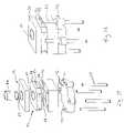
- an alternative systemshown generally at 70 , includes a lens 40 , such as a GRIN lens, that is optically coupled to an imaging array 48 of an SSID 38 .
- the lenscan be coupled to the imaging array by a clear adhesive material.
- Conductive padsare also present on the SSID and are configured to provide electrical signal, power, ground, and/or control to and from the SSID.
- the SSID 38can comprise a silicon or silicon-like substrate or amorphous silicon thin film transistors (TFT) having features typically manufactured therein.
- TFTthin film transistors
- the connection between conductive pads and the adaptor 52can be through soldering, wire bonding, solder bumping, eutectic bonding, electroplating, and conductive epoxy.
- a direct solder jointhaving no wire bonding between the conductive strips and the conductive pads can be preferred, as good steerability can be achieved with less risk of breaking electrical bonding.
- the umbilicalcan provide power, ground, clock signal, and output signal to the SSID through the adaptor.
- Other integrated circuit componentscan also be present for desired applications, such as light emitting diodes (LEDs) (not shown) for providing light to areas around the GRIN lens. If LEDs are present on the SSID, the adaptor can be of a clear material to allow light to pass therethrough. As the above described component are exemplary, it is not required that all of these components be present, as long as there is a visual or photon data gathering means, and some means of converting that data to a visual image or a visual reconstruction.
- the SSIDcan be any solid state imaging device, such as a CCD, a CID, or a CMOS imaging device.
- the lens 40can be a GRIN lens coated with an opaque coating on the curved surface to prevent light from entering the lens at other than the flat surface that is most distal with respect to the SSID.
- the adaptorcan provide a similar function as provided by the opaque coating.
- the adaptor 52includes four conductive strips 56 that are configured to electrically communicate in an “around the corner” configuration.
- the conductive stripsare positioned to contact the conductive pads 42 on the SSID 38 , once the adaptor and the SSID are mated together.
- an umbilical 30 containing conductive wires 32can be electrically coupled to the conductive strips.
- the conductive padsWhen assembled, by innervating the conductive strips with the conductive wires, the conductive pads are thus energized, thereby providing power, signal, ground, and/or control to and from the SSID.
- a lens 40is supported by a connector block or adaptor 52 , and a supplemental lens holder 76 .
- the adaptor and the supplemental lens holderare configured to accept and hold the GRIN lens via respective openings 68 , 69 .
- the adaptorcan comprise two different materials.
- a first materialcan be a non-conductive material that forms the substrate 78 .
- the substratesupports one or more conductive strips 56 formed of an electrically conductive material, such as a metal.
- the conductive stripsact to provide electrical contact between an umbilical, which comprises insulated conductive wires 32 in this embodiment, and conductive pads 42 present on the SSID 38 .
- the conductive wirescan be coupled to the conductive strips using a conductive bonding material, such as silver or gold filled epoxy, silver or gold solder, or another suitable adhesive or eutectic conductive substance.
- Each of the conductive wires 32can also be supported in a proper position by a wire guide 72 , and more specifically, by feeding each wire through lumens 74 defined by the wire guide.
- the conductive wiresprovide electrical contact through an umbilical between the adaptor 52 (and ultimately the SSID chip) and a computer interface (not shown), linking the SSID with another structure, e.g. a power source, signal processor, ground, or controller (not shown).
- the conductive wirescan also be used as tensioning wires to provide steerability. However, this is not required, as other means of controlling the direction of pointing of a head of the camera can be implemented.
- Each of the conductive strips 56is configured to transfer current from a location on a side of the adaptor 52 to a location on a bottom surface of the adaptor. More detail concerning the conductive strips can be appreciated with reference to FIGS. 19 and 20 . Still referring to FIGS. 17 and 18 , the conductive pads 42 are electrically coupled to an imaging array 48 of the SSID 38 . Additionally, each of the conductive wires 32 are electrically coupled to a corresponding conductive strip 56 .
- electrical power and data signalscan be sent to and from a source (not shown), through the conductive wires of the umbilical, through corresponding conductive strips, through corresponding conductive pads, and to and from the imaging array.
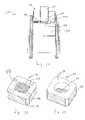
- a system shown generally at 80includes a distal tip portion 15 of an imaging catheter comprising a lens 40 , such as a GRIN lens.
- the lensis supported laterally by a connector block or adaptor 52 .
- a supplemental lens holder as described previouslycan also be used, but is not present in this embodiment.
- the adaptorhas a dual function, including providing support for the lens, and providing electrical communication between an electrical umbilical 30 and an SSID 38 .
- the adaptortypically includes a non-conductive substrate material 78 and a conductive strip 56 .
- the non-conductive substrate materialcan be a refractory and/or polymeric material such as SU-8 polymer material manufactured by IBM, Foturan which is a photosensitive glass manufactured by Corning, polymethyl methacrylate (PMMA) molded by Lithographie Galvanoformung Abformung (LIGA), or oxidized deep reactive ion etched (DRIE) silicon.
- the materialcan be substantially transparent so that verification of bonding of the adaptor to the SSID can be more easily obtained by visual inspection, such as by a microscope. If the SSID has a light source, such as an LED incorporated in it, the transparent block material enables the transmission of light forward.
- Conductive stripsare also attached to the adaptor, and thus, a path of electrical conductivity can be effectuated around a corner from a side surface to a bottom surface of the adaptor.
- Central aperture 69 for supporting the lensis also included in the adaptor.
- An electrical umbilical 30can comprise an insulator coating portion 88 .
- the conductive wiresare supported by a wire guide 72 having multiple lumen 74 .
- the insulator coating portionis removed adjacent the distal ends of the wires. This is done to provide a means of contacting the conductive wires 32 with the conductive strips 56 , so that electrical contact and communication can be provided between the SSID 38 and the power source, controller, and/or processor (not shown) through the conductive wires.
- each conductive wireis attached to a conductive strip at a side surface, and is held in electrical contact therewith by a conductive bonding material 82 that can be used to electrically couple two conductive lines, such as that discussed above.
- the conductive strip 56also contacts the conductive pad 42 of the SSID 38 . This contact is also fixed by the use of a conductive bonding material 84 , such as that described previously.
- the SSIDcan comprise an imaging array 48 , additional I.C. elements (not shown), conductive pads, and an electrical connection 86 between the connective pads and the imaging array. Additionally, the SSID can further include a microprocessor as well as light sources, such as LED's, as described above.
- the lens 40can be in close proximity or in contact with the imaging array 48 as the lens directs and focuses light or photons onto the imaging array.
- the conductive wires 32(two of which are not shown in a four wire umbilical system), can provide the dual function of guiding the direction the SSID, as well as provide electrical contact between any power source/signal processors (not shown) and the SSID at distal tip 15 of the catheter, though this dual functionality is not required.
- steeringcan be by a micromachined tube, as is known in the art.
- the components of a miniature imaging devicecan be fused together or bonded together as desired.
- an epoxysuch as a UV cure epoxy
- Other locations where an epoxy or other bonding material can be used to hold components togetherinclude the interface between the lens and the adaptor 52 , the interface between the substrate of the SSID and the wire guide 72 , and between the wire guide and the electrical umbilical 30 (which may or may not also act as tensioning wires).
- the wire guidecan also be bonded to the rest of the catheter (not shown) in this manner.
- the very small adaptor 52that not only acts hold the lens 40 in place over an SSID 38 , but also provides a conductive path for transporting electrical power, ground, control, and/or data signals from the conductive wires adjacent a side surface to the conductive pads 42 on the SSID.
- the adaptorprovides other advantages. For example, with this configuration, positioning and alignment of the lens on the SSID is more easily accomplished. This is particularly true since the size of this imagine device can be made smaller than about 0.5 mm in total width. Additionally, because the wires are attached to the adaptor on a side surface, there is no need to bend the electrical wires. This provides better strength and easier assembly for the connections for the wires, and for the miniature-imaging device as a whole. Thus, in this embodiment, the configuration of the adaptor facilitates the manufacturing of a very small imaging device.
- FIGS. 21 a - hdepict the manufacture of two adaptors. This is shown as exemplary, as one can be made individually, or alternatively, more than two can be made together, either by the process described below or by other known chip manufacturing processes. The figures are shown in cross section, and one of the two adaptors is shown along line 2 - 2 of FIG. 20 . FIGS. 21 a - h will be discussed collectively and sequentially.
- a substrate 102is provided that will be used to make an adaptor.
- the substratecan be, for example, a silicon wafer.
- a removable layer 104can be a thermal silicon dioxide layer.
- An appropriate thicknesscan be about 0.5 microns. This provides a working base to fabricate one or more primary lens holders.
- a polymer layer 106such as SU-8 manufactured by IBM, can be spun onto the silicon dioxide layer having a desired thickness dimension. Next, the layers are selectively exposed to UV light, in the presence of a mask, to form desired structure. These polymer blocks can each become the substrate of an adaptor.
- An example sizecan be a structure having a height of 300 microns, a length of 360 microns and a width of 380 microns.
- the center aperture that will hold the lenscan be about 300 microns in diameter. Thus, if the length is 360 microns, and the aperture is 300 microns in diameter, a 30 to 35 micron distance between the edge of the aperture and the edge of the polymer is all that may be present in this embodiment.
- the dimensions aboveare given by way of example. However, larger and even smaller blocks can be fabricated in accordance with the methods described herein.
- a metal trace material 108is sputtered or evaporated at an appropriate thickness.
- the metal trace materialwill ultimately become the conductive strip.
- Goldfor example, can be used as the metal trace material.
- the appropriate thickness of the deposited metal tracedepends upon the size of the SSID being made. However, commensurate with the present example, a thickness of about 0.5 microns can be used.
- a photoresist material 110can now be added atop the metal trace material.
- the photoresist materialcan be any material that can be altered when exposed to energy, such as heat and UV light. Further, the photoresist material can be diluted to achieve a desired result, depending on the application.
- a photoresist materialcan be used that is sensitive to heat by way of evaporation of a solvent.
- the UV lightcan be used to selectively expose the photoresist such that the UV exposed photoresist can be developed away in a developer (using positive photoresist), or the underexposed photoresist can developed away in a developer (using negative photoresist).
- the photoresistcan evaporate off at different speeds, leaving the photoresist material configured such as that shown in FIG. 21 b .
- the thickness differentialcan be as much as 10 fold or more, e.g., 2 microns in some areas and 20 microns in other areas.
- FIG. 21 cthe photoresist material is removed such that an exposed section of the metal trace element can be removed by, for example, wet etching or dry etching.
- FIG. 21 dshows the state of the photoresist material after portions are removed as described above.
- FIG. 21 ethe photoresist material is completely removed.
- the photoresist materialcan be removed by using a material known to react with the chosen photoresist material. In one embodiment, acetone can be used to remove the photoresist material.
- a saw cut 112can be made into the substrate, e.g., approximately through half of the substrate using a chip fab saw, for example.
- This stepcreates an opening for removal of the removable layer 104 , as shown in FIG. 21 g .
- the removable layer 104is silicon dioxide
- hydrofluoric acid (HF)can be used to react with the removable layer, releasing the polymer 106 from its connection with the substrate.
- the metal trace sections 108 that are not adhered to the polymer 106can be broken off as shown in FIG. 21 h .
- two adaptors 52remain separated from the substrate 102 , each of which can be used in conjunction with a catheter borne SSID such as that described above.
- optically coupledalso provides additional means of collecting light from GRIN lens and coupling it to an imaging array of an SSID.
- other optical devicescan be interposed between a GRIN lens and an SSID, such as a color filter, fiber optic, or any shape optical lens including a prism or wide angle lens.
- the fiber optic, or any shape optical lens including a prism or wide angle lenscan be placed on top of the GRIN lens in one embodiment.
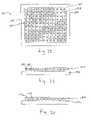
- a system of converting monochrome imaging to colorcan be accomplished by utilizing a filter having a predetermined pattern, such as a Bayer filter pattern.
- the basic building block of a Bayer filter patternis a 2 ⁇ 2 pattern having 1 blue (B), 1 red (R), and 2 green (G) squares.
- An advantage of using a Bayer filter patternis that only one sensor is required and all color information can be recorded simultaneously, providing for a smaller and cheaper design.
- demosaicing algorithmscan be used to convert the mosaic of separate colors into an equally sized mosaic of true colors. Each color pixel can be used more than once, and the true color of a single pixel can be determined by averaging the values from the closest surrounding pixels.
- a color filter insertshown generally at 150 , can comprise a substantially optically clear filter substrate 152 and a color filter mosaic portion 154 .
- the filter insert as a wholeis made up of green transparent color material 156 , blue transparent color material 158 , and red transparent color material 160 .
- Each of the transparent color material 156 , 158 , 160can be polymerized color resins such as those available from Brewer Science.
- the green color material 156can be put down on the clear filter substrate first, then the red 160 and blue 158 color material can be positioned in the appropriate spaces provided by the green material.
- Each transparent color materialcan be configured to be the size of an SSID image array pixel.
- the optically clear filter substratecan be, for example, a polymeric material such as SU-8 available from IBM, having a thickness of about 20 microns, though other thicknesses and materials can be used.
- a system 170including a color filter insert 150 having an optical clear filter substrate 152 and the color filter mosaic portion 154 , can be positioned between a lens 40 and an imaging array 48 of an SSID 38 .
- Any bonding technique or mechanical couplingcan be used to connect the SSID to the lens through the color filter insert or fiber optic in order to make the optical connection, such as bonding by an optically clear bonding epoxy.
- Other structuresare shown in FIG. 25 that are similar to those described with respect to FIG. 19 .
- FIGS. 26 and 27depict one possible relationship between a color filter insert 150 and an adaptor 52 (where the color filter can be integrated directly on the adaptor) from a bottom perspective view and a top perspective view, respectively.
- the adaptorincludes a substrate 78 and conductive strips 56 , as previously described.
- an imaging device in accordance with principles of the inventioncan be made very small, and is useful in solving certain imaging problems, particularly, that of imaging a remote location within or beyond a small opening, for example in human anatomy distal of a small orifice or luminal space (anatomical or artificial, such as a trocar lumen), or via a small incision, etc.
- these camerascan be made to be micron-sized for reaching areas previously inaccessible, such as dental/orthodontics, fallopian tubes, heart, lungs, vestibular region of ear, and the like. Larger lumens or cavities can be view with a greater degree of comfort and less patient duress, including the colon, stomach, esophagus, or any other similar anatomical structures. Additionally, such devices can be used for in situ tissue analysis.
Landscapes
- Health & Medical Sciences (AREA)
- Life Sciences & Earth Sciences (AREA)
- Surgery (AREA)
- Engineering & Computer Science (AREA)
- Radiology & Medical Imaging (AREA)
- Heart & Thoracic Surgery (AREA)
- Biophysics (AREA)
- Nuclear Medicine, Radiotherapy & Molecular Imaging (AREA)
- Optics & Photonics (AREA)
- Pathology (AREA)
- Veterinary Medicine (AREA)
- Public Health (AREA)
- Biomedical Technology (AREA)
- Physics & Mathematics (AREA)
- Medical Informatics (AREA)
- Molecular Biology (AREA)
- Animal Behavior & Ethology (AREA)
- General Health & Medical Sciences (AREA)
- Multimedia (AREA)
- Signal Processing (AREA)
- Endoscopes (AREA)
Abstract
Description
Claims (18)
Priority Applications (11)
| Application Number | Priority Date | Filing Date | Title |
|---|---|---|---|
| US10/391,513US7591780B2 (en) | 2002-03-18 | 2003-03-17 | Miniaturized imaging device with integrated circuit connector system |
| EP05021748AEP1626436A3 (en) | 2002-03-18 | 2003-03-18 | Method of making a solid state imaging device |
| EP05021747AEP1626588A3 (en) | 2002-03-18 | 2003-03-18 | Miniaturized imaging device |
| AU2003222014AAU2003222014A1 (en) | 2002-03-18 | 2003-03-18 | Miniaturized imaging device |
| JP2003579407AJP4574169B2 (en) | 2002-03-18 | 2003-03-18 | Small imaging device |
| PCT/US2003/008312WO2003081831A2 (en) | 2002-03-18 | 2003-03-18 | Miniaturized imaging device |
| EP03717997AEP1486077A4 (en) | 2002-03-18 | 2003-03-18 | Miniaturized imaging device |
| US11/062,201US7166537B2 (en) | 2002-03-18 | 2005-02-17 | Miniaturized imaging device with integrated circuit connector system |
| US11/292,902US20060146172A1 (en) | 2002-03-18 | 2005-12-01 | Miniaturized utility device having integrated optical capabilities |
| US12/079,741US7629659B2 (en) | 2002-03-18 | 2008-03-27 | Miniaturized imaging device with integrated circuit connector system |
| JP2009195048AJP4903844B2 (en) | 2002-03-18 | 2009-08-26 | Small imaging device |
Applications Claiming Priority (4)
| Application Number | Priority Date | Filing Date | Title |
|---|---|---|---|
| US36569202P | 2002-03-18 | 2002-03-18 | |
| US36556102P | 2002-03-18 | 2002-03-18 | |
| US43126102P | 2002-12-06 | 2002-12-06 | |
| US10/391,513US7591780B2 (en) | 2002-03-18 | 2003-03-17 | Miniaturized imaging device with integrated circuit connector system |
Related Parent Applications (1)
| Application Number | Title | Priority Date | Filing Date |
|---|---|---|---|
| US39148903AContinuation-In-Part | 2002-03-18 | 2003-03-17 |
Related Child Applications (3)
| Application Number | Title | Priority Date | Filing Date |
|---|---|---|---|
| US11/062,201DivisionUS7166537B2 (en) | 2002-03-18 | 2005-02-17 | Miniaturized imaging device with integrated circuit connector system |
| US11/292,902Continuation-In-PartUS20060146172A1 (en) | 2002-03-18 | 2005-12-01 | Miniaturized utility device having integrated optical capabilities |
| US12/079,741DivisionUS7629659B2 (en) | 2002-03-18 | 2008-03-27 | Miniaturized imaging device with integrated circuit connector system |
Publications (2)
| Publication Number | Publication Date |
|---|---|
| US20030222325A1 US20030222325A1 (en) | 2003-12-04 |
| US7591780B2true US7591780B2 (en) | 2009-09-22 |
Family
ID=29587845
Family Applications (3)
| Application Number | Title | Priority Date | Filing Date |
|---|---|---|---|
| US10/391,513Expired - LifetimeUS7591780B2 (en) | 2002-03-18 | 2003-03-17 | Miniaturized imaging device with integrated circuit connector system |
| US11/062,201Expired - LifetimeUS7166537B2 (en) | 2002-03-18 | 2005-02-17 | Miniaturized imaging device with integrated circuit connector system |
| US12/079,741Expired - LifetimeUS7629659B2 (en) | 2002-03-18 | 2008-03-27 | Miniaturized imaging device with integrated circuit connector system |
Family Applications After (2)
| Application Number | Title | Priority Date | Filing Date |
|---|---|---|---|
| US11/062,201Expired - LifetimeUS7166537B2 (en) | 2002-03-18 | 2005-02-17 | Miniaturized imaging device with integrated circuit connector system |
| US12/079,741Expired - LifetimeUS7629659B2 (en) | 2002-03-18 | 2008-03-27 | Miniaturized imaging device with integrated circuit connector system |
Country Status (1)
| Country | Link |
|---|---|
| US (3) | US7591780B2 (en) |
Cited By (22)
| Publication number | Priority date | Publication date | Assignee | Title |
|---|---|---|---|---|
| US20100185052A1 (en)* | 2009-01-19 | 2010-07-22 | Hui-Yu Chang | Endoscopic device |
| US20100321564A1 (en)* | 2004-04-08 | 2010-12-23 | Feldman Michael R | Camera system and associated methods |
| US7969659B2 (en)* | 2008-01-11 | 2011-06-28 | Sterling Lc | Grin lens microscope system |
| US20120310043A1 (en)* | 2011-06-06 | 2012-12-06 | Fujikura Ltd. | Structure of imaging part in electronic visualized catheter |
| US8358462B2 (en) | 2007-06-05 | 2013-01-22 | Jacobsen Stephen C | Mini-scope for multi-directional imaging |
| US8486735B2 (en) | 2008-07-30 | 2013-07-16 | Raytheon Company | Method and device for incremental wavelength variation to analyze tissue |
| US8614768B2 (en) | 2002-03-18 | 2013-12-24 | Raytheon Company | Miniaturized imaging device including GRIN lens optically coupled to SSID |
| US8690762B2 (en) | 2008-06-18 | 2014-04-08 | Raytheon Company | Transparent endoscope head defining a focal length |
| US8717428B2 (en) | 2009-10-01 | 2014-05-06 | Raytheon Company | Light diffusion apparatus |
| US8828028B2 (en) | 2009-11-03 | 2014-09-09 | Raytheon Company | Suture device and method for closing a planar opening |
| USD716841S1 (en) | 2012-09-07 | 2014-11-04 | Covidien Lp | Display screen with annotate file icon |
| USD717340S1 (en) | 2012-09-07 | 2014-11-11 | Covidien Lp | Display screen with enteral feeding icon |
| US9060704B2 (en) | 2008-11-04 | 2015-06-23 | Sarcos Lc | Method and device for wavelength shifted imaging |
| USD735343S1 (en) | 2012-09-07 | 2015-07-28 | Covidien Lp | Console |
| US9144664B2 (en) | 2009-10-01 | 2015-09-29 | Sarcos Lc | Method and apparatus for manipulating movement of a micro-catheter |
| US9198835B2 (en) | 2012-09-07 | 2015-12-01 | Covidien Lp | Catheter with imaging assembly with placement aid and related methods therefor |
| US9377565B2 (en) | 2012-08-10 | 2016-06-28 | Corning Cable Systems Llc | Processing of gradient index (GRIN) rods into GRIN lenses attachable to optical devices, components, and methods |
| US9433339B2 (en) | 2010-09-08 | 2016-09-06 | Covidien Lp | Catheter with imaging assembly and console with reference library and related methods therefor |
| US9506722B2 (en)* | 2010-06-18 | 2016-11-29 | Nitesite Ltd. | Viewing apparatus |
| US9517184B2 (en) | 2012-09-07 | 2016-12-13 | Covidien Lp | Feeding tube with insufflation device and related methods therefor |
| US9661996B2 (en) | 2009-10-01 | 2017-05-30 | Sarcos Lc | Needle delivered imaging device |
| US9848764B2 (en) | 2012-03-22 | 2017-12-26 | Integra Lifesciences Switzerland Sàrl | Fluid management catheter and methods of using same |
Families Citing this family (75)
| Publication number | Priority date | Publication date | Assignee | Title |
|---|---|---|---|---|
| US7591780B2 (en) | 2002-03-18 | 2009-09-22 | Sterling Lc | Miniaturized imaging device with integrated circuit connector system |
| US7787939B2 (en) | 2002-03-18 | 2010-08-31 | Sterling Lc | Miniaturized imaging device including utility aperture and SSID |
| US20060146172A1 (en)* | 2002-03-18 | 2006-07-06 | Jacobsen Stephen C | Miniaturized utility device having integrated optical capabilities |
| US7698068B2 (en) | 2004-06-17 | 2010-04-13 | Cadent Ltd. | Method for providing data associated with the intraoral cavity |
| US8050746B2 (en) | 2005-02-02 | 2011-11-01 | Voyage Medical, Inc. | Tissue visualization device and method variations |
| US7918787B2 (en)* | 2005-02-02 | 2011-04-05 | Voyage Medical, Inc. | Tissue visualization and manipulation systems |
| US11478152B2 (en) | 2005-02-02 | 2022-10-25 | Intuitive Surgical Operations, Inc. | Electrophysiology mapping and visualization system |
| US7860556B2 (en)* | 2005-02-02 | 2010-12-28 | Voyage Medical, Inc. | Tissue imaging and extraction systems |
| US8078266B2 (en) | 2005-10-25 | 2011-12-13 | Voyage Medical, Inc. | Flow reduction hood systems |
| US20080015569A1 (en) | 2005-02-02 | 2008-01-17 | Voyage Medical, Inc. | Methods and apparatus for treatment of atrial fibrillation |
| US9510732B2 (en) | 2005-10-25 | 2016-12-06 | Intuitive Surgical Operations, Inc. | Methods and apparatus for efficient purging |
| US8137333B2 (en) | 2005-10-25 | 2012-03-20 | Voyage Medical, Inc. | Delivery of biological compounds to ischemic and/or infarcted tissue |
| US7930016B1 (en) | 2005-02-02 | 2011-04-19 | Voyage Medical, Inc. | Tissue closure system |
| US10064540B2 (en) | 2005-02-02 | 2018-09-04 | Intuitive Surgical Operations, Inc. | Visualization apparatus for transseptal access |
| US7860555B2 (en) | 2005-02-02 | 2010-12-28 | Voyage Medical, Inc. | Tissue visualization and manipulation system |
| JP2006251691A (en)* | 2005-03-14 | 2006-09-21 | Oki Electric Ind Co Ltd | Manufacturing method of optical element |
| US8221310B2 (en) | 2005-10-25 | 2012-07-17 | Voyage Medical, Inc. | Tissue visualization device and method variations |
| US8043209B2 (en)* | 2006-06-13 | 2011-10-25 | Given Imaging Ltd. | System and method for transmitting the content of memory storage in an in-vivo sensing device |
| US9055906B2 (en) | 2006-06-14 | 2015-06-16 | Intuitive Surgical Operations, Inc. | In-vivo visualization systems |
| US20080033241A1 (en)* | 2006-08-01 | 2008-02-07 | Ruey-Feng Peh | Left atrial appendage closure |
| WO2008028149A2 (en) | 2006-09-01 | 2008-03-06 | Voyage Medical, Inc. | Electrophysiology mapping and visualization system |
| US20080097476A1 (en) | 2006-09-01 | 2008-04-24 | Voyage Medical, Inc. | Precision control systems for tissue visualization and manipulation assemblies |
| US10004388B2 (en) | 2006-09-01 | 2018-06-26 | Intuitive Surgical Operations, Inc. | Coronary sinus cannulation |
| US10335131B2 (en) | 2006-10-23 | 2019-07-02 | Intuitive Surgical Operations, Inc. | Methods for preventing tissue migration |
| US20080183036A1 (en) | 2006-12-18 | 2008-07-31 | Voyage Medical, Inc. | Systems and methods for unobstructed visualization and ablation |
| US9226648B2 (en) | 2006-12-21 | 2016-01-05 | Intuitive Surgical Operations, Inc. | Off-axis visualization systems |
| US8131350B2 (en) | 2006-12-21 | 2012-03-06 | Voyage Medical, Inc. | Stabilization of visualization catheters |
| EP2148608A4 (en) | 2007-04-27 | 2010-04-28 | Voyage Medical Inc | Complex shape steerable tissue visualization and manipulation catheter |
| US8657805B2 (en) | 2007-05-08 | 2014-02-25 | Intuitive Surgical Operations, Inc. | Complex shape steerable tissue visualization and manipulation catheter |
| WO2008141238A1 (en) | 2007-05-11 | 2008-11-20 | Voyage Medical, Inc. | Visual electrode ablation systems |
| US20090030276A1 (en)* | 2007-07-27 | 2009-01-29 | Voyage Medical, Inc. | Tissue visualization catheter with imaging systems integration |
| US20090062790A1 (en)* | 2007-08-31 | 2009-03-05 | Voyage Medical, Inc. | Direct visualization bipolar ablation systems |
| US8235985B2 (en) | 2007-08-31 | 2012-08-07 | Voyage Medical, Inc. | Visualization and ablation system variations |
| US20090125022A1 (en)* | 2007-11-12 | 2009-05-14 | Voyage Medical, Inc. | Tissue visualization and ablation systems |
| US20090143640A1 (en)* | 2007-11-26 | 2009-06-04 | Voyage Medical, Inc. | Combination imaging and treatment assemblies |
| US20090160965A1 (en)* | 2007-12-20 | 2009-06-25 | Samsung Electronics Co., Ltd. | Image sensor having a diffractive optics element |
| US8858609B2 (en) | 2008-02-07 | 2014-10-14 | Intuitive Surgical Operations, Inc. | Stent delivery under direct visualization |
| US8892182B2 (en)* | 2008-02-08 | 2014-11-18 | Ethicon, Inc. | Double balloon isolation catheters and methods therefor |
| US8529441B2 (en) | 2008-02-12 | 2013-09-10 | Innurvation, Inc. | Ingestible endoscopic optical scanning device |
| US20090287048A1 (en)* | 2008-05-16 | 2009-11-19 | Sterling Lc | Method and apparatus for imaging within a living body |
| US20090326321A1 (en)* | 2008-06-18 | 2009-12-31 | Jacobsen Stephen C | Miniaturized Imaging Device Including Multiple GRIN Lenses Optically Coupled to Multiple SSIDs |
| US20090326572A1 (en)* | 2008-06-27 | 2009-12-31 | Ruey-Feng Peh | Apparatus and methods for rapid tissue crossing |
| US9101735B2 (en) | 2008-07-07 | 2015-08-11 | Intuitive Surgical Operations, Inc. | Catheter control systems |
| US20100016844A1 (en)* | 2008-07-21 | 2010-01-21 | Patel Jr Manoj B | Transilluminating foley catheter to facilitate prostate and bladder surgery |
| EP2327122A4 (en)* | 2008-09-15 | 2013-07-24 | Pacific Aerospace & Electronics Inc | Connector assemblies incorporating ceramic inserts having conductive pathways and interfaces |
| US8333012B2 (en) | 2008-10-10 | 2012-12-18 | Voyage Medical, Inc. | Method of forming electrode placement and connection systems |
| US8894643B2 (en) | 2008-10-10 | 2014-11-25 | Intuitive Surgical Operations, Inc. | Integral electrode placement and connection systems |
| US9468364B2 (en) | 2008-11-14 | 2016-10-18 | Intuitive Surgical Operations, Inc. | Intravascular catheter with hood and image processing systems |
| US9717403B2 (en) | 2008-12-05 | 2017-08-01 | Jeffrey B. Kleiner | Method and apparatus for performing retro peritoneal dissection |
| US8864654B2 (en)* | 2010-04-20 | 2014-10-21 | Jeffrey B. Kleiner | Method and apparatus for performing retro peritoneal dissection |
| US20100256629A1 (en)* | 2009-04-06 | 2010-10-07 | Voyage Medical, Inc. | Methods and devices for treatment of the ostium |
| JP5453947B2 (en)* | 2009-06-17 | 2014-03-26 | ソニー株式会社 | Manufacturing method of solid-state imaging device |
| CA2763826C (en) | 2009-06-17 | 2020-04-07 | 3Shape A/S | Focus scanning apparatus |
| US20120119661A1 (en)* | 2009-11-25 | 2012-05-17 | Delo Industrial Adhesives Llc | Light emitting diode operating device and method |
| US8694071B2 (en) | 2010-02-12 | 2014-04-08 | Intuitive Surgical Operations, Inc. | Image stabilization techniques and methods |
| US9814522B2 (en) | 2010-04-06 | 2017-11-14 | Intuitive Surgical Operations, Inc. | Apparatus and methods for ablation efficacy |
| US10582834B2 (en)* | 2010-06-15 | 2020-03-10 | Covidien Lp | Locatable expandable working channel and method |
| US9788755B2 (en)* | 2011-05-26 | 2017-10-17 | Covidien Lp | Illumination systems and devices for tracheal tubes |
| US8890945B2 (en)* | 2011-11-14 | 2014-11-18 | Omnivision Technologies, Inc. | Shared terminal of an image sensor system for transferring image data and control signals |
| US8953083B2 (en)* | 2012-02-13 | 2015-02-10 | Apple Inc. | Housing camera lens cover using GRIN technology |
| US8916980B2 (en)* | 2012-02-16 | 2014-12-23 | Omnivision Technologies, Inc. | Pad and circuit layout for semiconductor devices |
| JP5558600B2 (en)* | 2012-03-13 | 2014-07-23 | 富士フイルム株式会社 | Endoscope board connector, endoscope and manufacturing method thereof |
| US20140012078A1 (en)* | 2012-07-05 | 2014-01-09 | Raymond Coussa | Accelorometer Based Endoscopic Light Source Safety System |
| WO2015042529A2 (en)* | 2013-09-20 | 2015-03-26 | The Regents Of The University Of California | Methods, systems, and devices for imaging microscopic tumors |
| WO2015050044A1 (en)* | 2013-10-04 | 2015-04-09 | オリンパスメディカルシステムズ株式会社 | Image pickup unit for endoscope |
| US10010387B2 (en) | 2014-02-07 | 2018-07-03 | 3Shape A/S | Detecting tooth shade |
| US9675430B2 (en) | 2014-08-15 | 2017-06-13 | Align Technology, Inc. | Confocal imaging apparatus with curved focal surface |
| EP4233738B1 (en) | 2015-05-29 | 2025-07-23 | Microvention, Inc. | Catheter circuit |
| US10485404B2 (en)* | 2016-03-01 | 2019-11-26 | Karl Storz Endovision, Inc. | Compact image sensor module and method of assembly for image sensor modules |
| WO2019077755A1 (en)* | 2017-10-20 | 2019-04-25 | オリンパス株式会社 | Endoscope leading tip, endoscope, and method for producing endoscope leading tip |
| WO2020121435A1 (en)* | 2018-12-12 | 2020-06-18 | オリンパス株式会社 | Endoscope tip and endoscope |
| US11986163B2 (en)* | 2018-12-28 | 2024-05-21 | Hoya Corporation | Endoscope and endoscope system controlled by pair of cable bundles |
| US20200316349A1 (en)* | 2019-04-03 | 2020-10-08 | Fraser M. Smith | Micro-Camera Guide Wire |
| US12121211B2 (en)* | 2019-11-22 | 2024-10-22 | Lake Region Manufacturing, Inc. | Guidewire and catheter system for in-vivo forward viewing of the vasculature |
| CN116419706A (en)* | 2020-09-25 | 2023-07-11 | 波士顿科学国际有限公司 | medical imaging device |
Citations (159)
| Publication number | Priority date | Publication date | Assignee | Title |
|---|---|---|---|---|
| US3971065A (en) | 1975-03-05 | 1976-07-20 | Eastman Kodak Company | Color imaging array |
| US4283115A (en) | 1978-06-28 | 1981-08-11 | Richard Wolf Gmbh | Beam splitters for endoscopes comprising a dual observation system |
| JPS5846924Y2 (en) | 1979-11-14 | 1983-10-26 | マツダ株式会社 | Device to prevent forgetting to remove the key from a vehicle |
| US4487206A (en) | 1982-10-13 | 1984-12-11 | Honeywell Inc. | Fiber optic pressure sensor with temperature compensation and reference |
| US4515444A (en) | 1983-06-30 | 1985-05-07 | Dyonics, Inc. | Optical system |
| US4573450A (en) | 1983-11-11 | 1986-03-04 | Fuji Photo Optical Co., Ltd. | Endoscope |
| US4604992A (en) | 1983-12-27 | 1986-08-12 | Olympus Optical Company, Ltd. | Endoscope system |
| US4620534A (en) | 1984-11-01 | 1986-11-04 | New Mexico State University Foundation | Apparatus for insertion of an intravaginal article |
| US4622954A (en) | 1984-05-15 | 1986-11-18 | Fuji Photo Optical Co., Ltd. | Endoscope having a plate-like image sensor for forming images |
| US4646724A (en) | 1982-10-15 | 1987-03-03 | Olympus Optical Co., Ltd. | Endoscopic photographing apparatus |
| US4706118A (en) | 1985-10-09 | 1987-11-10 | Olympus Optical Co., Ltd. | Control circuit for video endoscope |
| US4723843A (en) | 1985-07-31 | 1988-02-09 | Richard Wolf Gmbh | Endoscope optical system |
| US4745470A (en) | 1986-04-04 | 1988-05-17 | Olympus Optical Co., Ltd. | Endoscope using a chip carrier type solid state imaging device |
| US4745471A (en) | 1986-05-13 | 1988-05-17 | Olympus Optical Co., Ltd. | Solid-state imaging apparatus and endoscope |
| JPS63155115U (en) | 1987-03-30 | 1988-10-12 | ||
| US4791479A (en) | 1986-06-04 | 1988-12-13 | Olympus Optical Co., Ltd. | Color-image sensing apparatus |
| US4803562A (en) | 1986-06-20 | 1989-02-07 | Olympus Optical Co., Ltd. | Image sensing apparatus |
| US4802487A (en) | 1987-03-26 | 1989-02-07 | Washington Research Foundation | Endoscopically deliverable ultrasound imaging system |
| US4832003A (en)* | 1986-09-12 | 1989-05-23 | Olympus Optical Co., Ltd. | Electronic endoscope tip |
| US4846785A (en) | 1987-01-22 | 1989-07-11 | Robert Cassou | Instrument for artificial insemination, embryo transfer or sampling follicular liquids in mammals |
| US4859040A (en) | 1985-12-27 | 1989-08-22 | Canon Kabushiki Kaisha | Optical system having gradient-index lens and method for correcting aberrations |
| US4867137A (en) | 1987-03-19 | 1989-09-19 | Olympus Optical Co., Ltd. | Electronic endoscope |
| US4867174A (en) | 1987-11-18 | 1989-09-19 | Baxter Travenol Laboratories, Inc. | Guidewire for medical use |
| US4867138A (en) | 1987-05-13 | 1989-09-19 | Olympus Optical Co., Ltd. | Rigid electronic endoscope |
| US4880298A (en) | 1985-08-07 | 1989-11-14 | Olympus Optical Co., Ltd. | Microscope objective |
| US4895138A (en) | 1985-01-14 | 1990-01-23 | Olympus Optical Co., Ltd. | Endoscope with a detachable observation unit at its distal end |
| US4926257A (en) | 1986-12-19 | 1990-05-15 | Olympus Optical Co., Ltd. | Stereoscopic electronic endoscope device |
| US4932394A (en) | 1987-08-10 | 1990-06-12 | Kabushiki Kaisha Toshiba | Endoscope including scope terminal locking indicator |
| US4998807A (en) | 1988-08-23 | 1991-03-12 | Olympus Optical Co., Ltd. | Variable focal length lens system |
| US5006928A (en) | 1988-12-05 | 1991-04-09 | Fuji Photo Film Co., Ltd. | Image processing method in an electronic video endoscopy system |
| US5009483A (en) | 1989-04-12 | 1991-04-23 | Rockwell Iii Marshall A | Optical waveguide display system |
| US5021888A (en) | 1987-12-18 | 1991-06-04 | Kabushiki Kaisha Toshiba | Miniaturized solid state imaging device |
| US5040069A (en)* | 1989-06-16 | 1991-08-13 | Fuji Photo Optical Co., Ltd. | Electronic endoscope with a mask bump bonded to an image pick-up device |
| US5061036A (en) | 1990-04-17 | 1991-10-29 | Photon Imaging Corp. | Color page scanner using fiber optic bundle and a photosensor array |
| US5093719A (en) | 1989-10-23 | 1992-03-03 | Manx Optical Corporation | Endoscopic gradient index optical systems |
| US5106387A (en) | 1985-03-22 | 1992-04-21 | Massachusetts Institute Of Technology | Method for spectroscopic diagnosis of tissue |
| US5109859A (en) | 1989-10-04 | 1992-05-05 | Beth Israel Hospital Association | Ultrasound guided laser angioplasty |
| US5111804A (en) | 1989-02-15 | 1992-05-12 | Kabushiki Kaisha Toshiba | Electronic endoscope |
| US5113254A (en) | 1989-04-06 | 1992-05-12 | Olympus Optical Co., Ltd. | Electronic endoscope apparatus outputting ternary drive signal |
| US5130804A (en) | 1990-01-09 | 1992-07-14 | Konica Corporation | Compact recording apparatus with functional components mounted on a substrate |
| US5166656A (en) | 1992-02-28 | 1992-11-24 | Avx Corporation | Thin film surface mount fuses |
| US5191203A (en) | 1991-04-18 | 1993-03-02 | Mckinley Optics, Inc. | Stereo video endoscope objective lens system |
| US5198894A (en) | 1991-09-24 | 1993-03-30 | Hicks John W | Drape for endoscope |
| US5220198A (en) | 1990-08-27 | 1993-06-15 | Olympus Optical Co., Ltd. | Solid state imaging apparatus in which a solid state imaging device chip and substrate are face-bonded with each other |
| US5222477A (en) | 1991-09-30 | 1993-06-29 | Welch Allyn, Inc. | Endoscope or borescope stereo viewing system |
| US5228430A (en) | 1989-08-04 | 1993-07-20 | Kabushiki Kaisha Toshiba | Electronic endoscope apparatus including easy focusing distal end |
| JPH0549602B2 (en) | 1984-12-24 | 1993-07-26 | Dow Chemical Co | |
| US5258834A (en) | 1991-02-13 | 1993-11-02 | Olympus Optical Co., Ltd. | Electronic endoscope for producing a color image by extracting a plurality of field picture images in one field period without changing a horizontal clock rate |
| US5291010A (en) | 1990-10-04 | 1994-03-01 | Olympus Optical Co., Ltd. | Solid state imaging device having a chambered imaging chip corner |
| US5305098A (en) | 1991-04-11 | 1994-04-19 | Olympus Optical Co., Ltd. | Endoscope image processing system with means for discriminating between endoscope image area and character image area |
| US5304173A (en) | 1985-03-22 | 1994-04-19 | Massachusetts Institute Of Technology | Spectral diagonostic and treatment system |
| US5361166A (en) | 1993-01-28 | 1994-11-01 | Gradient Lens Corporation | Negative abbe number radial gradient index relay and use of same |
| US5365268A (en) | 1991-04-26 | 1994-11-15 | Fuji Photo Optical Co., Ltd. | Circuit board of solid-state image sensor for electronic endoscope |
| US5377047A (en) | 1992-04-13 | 1994-12-27 | Linvatec Corporation | Disposable endoscope employing positive and negative gradient index of refraction optical materials |
| US5381784A (en)* | 1992-09-30 | 1995-01-17 | Adair; Edwin L. | Stereoscopic endoscope |
| EP0639043A1 (en) | 1993-08-10 | 1995-02-15 | Siemens Nixdorf Informationssysteme AG | Process for manufacturing plated through-hole printed circuit boards having very small solder lands |
| US5396366A (en) | 1993-03-04 | 1995-03-07 | Sigma Dynamics Corporation | Endoscope apparatus |
| US5398685A (en) | 1992-01-10 | 1995-03-21 | Wilk; Peter J. | Endoscopic diagnostic system and associated method |
| US5402769A (en) | 1992-04-23 | 1995-04-04 | Olympus Optical Co., Ltd. | Endoscope apparatus which time-sequentially transmits sensor signals with image signals during a blanking period |
| US5430475A (en)* | 1990-06-29 | 1995-07-04 | Olympus Optical Co., Ltd. | Electronic endoscope apparatus having micro array on photoelectric conversion surface |
| US5434615A (en) | 1992-09-25 | 1995-07-18 | Fuji Photo Optical Co., Ltd. | Signal processing circuit adaptable to electronic endoscopes having different lengths |
| US5436655A (en) | 1991-08-09 | 1995-07-25 | Olympus Optical Co., Ltd. | Endoscope apparatus for three dimensional measurement for scanning spot light to execute three dimensional measurement |
| US5438975A (en) | 1993-03-24 | 1995-08-08 | Machida Endoscope Co., Ltd. | Distal tip of endoscope having spirally coiled control wires |
| US5455455A (en) | 1992-09-14 | 1995-10-03 | Badehi; Peirre | Methods for producing packaged integrated circuit devices and packaged integrated circuit devices produced thereby |
| US5459570A (en) | 1991-04-29 | 1995-10-17 | Massachusetts Institute Of Technology | Method and apparatus for performing optical measurements |
| EP0681809A1 (en) | 1994-05-09 | 1995-11-15 | Welch Allyn, Inc. | Stereo imaging assembly for endoscopic probe |
| US5469841A (en) | 1992-10-29 | 1995-11-28 | Olympus Optical Co., Ltd. | Endoscope apparatus provided with liquid removing mechanism for the electric connector |
| US5512940A (en) | 1993-03-19 | 1996-04-30 | Olympus Optical Co., Ltd. | Image processing apparatus, endoscope image sensing and processing apparatus, and image processing method for performing different displays depending upon subject quantity |
| US5531664A (en)* | 1990-12-26 | 1996-07-02 | Olympus Optical Co., Ltd. | Bending actuator having a coil sheath with a fixed distal end and a free proximal end |
| US5594497A (en) | 1993-04-07 | 1997-01-14 | Ahern; John M. | Endoscope provided with a distally located color CCD |
| US5603687A (en) | 1992-10-28 | 1997-02-18 | Oktas General Partnership | Asymmetric stereo-optic endoscope |
| US5630788A (en) | 1994-08-12 | 1997-05-20 | Imagyn Medical, Inc. | Endoscope with curved end image guide |
| US5647368A (en) | 1996-02-28 | 1997-07-15 | Xillix Technologies Corp. | Imaging system for detecting diseased tissue using native fluorsecence in the gastrointestinal and respiratory tract |
| US5673083A (en)* | 1989-03-17 | 1997-09-30 | Hitachi, Ltd. | Semiconductor device and video camera unit having the same and method for manufacturing the same |
| US5685311A (en) | 1994-10-20 | 1997-11-11 | Olympus Optical Company, Ltd. | Image display system |
| US5693043A (en) | 1985-03-22 | 1997-12-02 | Massachusetts Institute Of Technology | Catheter for laser angiosurgery |
| US5716323A (en) | 1995-04-05 | 1998-02-10 | Karl Storz Imaging | Electrical isolation of endoscopic video camera |
| US5716759A (en) | 1993-09-02 | 1998-02-10 | Shellcase Ltd. | Method and apparatus for producing integrated circuit devices |
| US5722403A (en) | 1996-10-28 | 1998-03-03 | Ep Technologies, Inc. | Systems and methods using a porous electrode for ablating and visualizing interior tissue regions |
| US5740808A (en) | 1996-10-28 | 1998-04-21 | Ep Technologies, Inc | Systems and methods for guilding diagnostic or therapeutic devices in interior tissue regions |
| US5749827A (en) | 1995-03-07 | 1998-05-12 | Fuji Photo Optical Co., Ltd. | Objective optical member with air gap for endoscope imaging unit |
| US5751340A (en) | 1996-08-21 | 1998-05-12 | Karl Storz Gmbh & Co. | Method and apparatus for reducing the inherently dark grid pattern from the video display of images from fiber optic bundles |
| US5752518A (en) | 1996-10-28 | 1998-05-19 | Ep Technologies, Inc. | Systems and methods for visualizing interior regions of the body |
| US5769792A (en) | 1991-07-03 | 1998-06-23 | Xillix Technologies Corp. | Endoscopic imaging system for diseased tissue |
| US5772597A (en) | 1992-09-14 | 1998-06-30 | Sextant Medical Corporation | Surgical tool end effector |
| US5776049A (en) | 1992-12-24 | 1998-07-07 | Olympus Optical Co., Ltd. | Stereo endoscope and stereo endoscope imaging apparatus |
| US5792984A (en)* | 1996-07-01 | 1998-08-11 | Cts Corporation | Molded aluminum nitride packages |
| US5800341A (en)* | 1994-03-30 | 1998-09-01 | Medical Media Systems | Electronically steerable endoscope |
| WO1998038907A1 (en) | 1997-03-06 | 1998-09-11 | Massachusetts Institute Of Technology | Instrument for optically scanning of living tissue |
| US5808665A (en) | 1992-01-21 | 1998-09-15 | Sri International | Endoscopic surgical instrument and method for use |
| US5818644A (en) | 1995-11-02 | 1998-10-06 | Olympus Optical Co., Ltd. | Gradient index optical element and method for making the same |
| US5827172A (en) | 1996-09-30 | 1998-10-27 | Fuji Photo Optical Co., Ltd. | Optical system for electronic endoscopes |
| US5840017A (en) | 1995-08-03 | 1998-11-24 | Asahi Kogaku Kogyo Kabushiki Kaisha | Endoscope system |
| US5848969A (en) | 1996-10-28 | 1998-12-15 | Ep Technologies, Inc. | Systems and methods for visualizing interior tissue regions using expandable imaging structures |
| US5865729A (en) | 1997-10-10 | 1999-02-02 | Olympus America, Inc. | Apparatus for facilitating gynecological examinations and procedures |
| US5873816A (en) | 1994-11-02 | 1999-02-23 | Olympus Optical Co., Ltd. | Electronic endoscope having an insertional portion a part of which is a conductive armor |
| US5879285A (en) | 1995-09-28 | 1999-03-09 | Olympus Optical Co., Ltd. | Aligning means attaching a cable in an imaging apparatus |
| EP0482997B1 (en) | 1990-10-23 | 1999-04-21 | Sony Corporation | Lens barrel having reference shafts for movably supporting lenses |
| US5904651A (en) | 1996-10-28 | 1999-05-18 | Ep Technologies, Inc. | Systems and methods for visualizing tissue during diagnostic or therapeutic procedures |
| US5908445A (en) | 1996-10-28 | 1999-06-01 | Ep Technologies, Inc. | Systems for visualizing interior tissue regions including an actuator to move imaging element |
| US5913817A (en) | 1995-04-05 | 1999-06-22 | Karl Storz Imaging | Electrical isolation of endoscopic video camera |
| US5929900A (en) | 1996-11-14 | 1999-07-27 | Fuji Photo Optical Co., Ltd. | Signal processor circuit for endoscope systems of all-pixels readout type |
| WO1999040624A1 (en) | 1998-02-06 | 1999-08-12 | Shellcase Ltd. | Integrated circuit device |
| US5940126A (en) | 1994-10-25 | 1999-08-17 | Kabushiki Kaisha Toshiba | Multiple image video camera apparatus |
| US5951462A (en) | 1997-12-11 | 1999-09-14 | Fuji Photo Optical Co., Ltd. | Electronic endoscope system for displaying unconnected scope |
| US5957849A (en) | 1997-06-30 | 1999-09-28 | The Regents Of The University Of California | Endoluminal ultrasound-guided resectoscope |
| US5973779A (en) | 1996-03-29 | 1999-10-26 | Ansari; Rafat R. | Fiber-optic imaging probe |
| US5971915A (en) | 1997-06-13 | 1999-10-26 | Fuji Photo Optical Co., Ltd. | Stereoscopic endoscope |
| US5980663A (en) | 1995-05-15 | 1999-11-09 | Shellcase Ltd. | Bonding machine |
| US5999327A (en) | 1995-09-12 | 1999-12-07 | Olympus Optical Co., Ltd. | Objective lens system |
| US6008123A (en) | 1997-11-04 | 1999-12-28 | Lucent Technologies Inc. | Method for using a hardmask to form an opening in a semiconductor substrate |
| US6022758A (en) | 1994-07-10 | 2000-02-08 | Shellcase Ltd. | Process for manufacturing solder leads on a semiconductor device package |
| US6040235A (en) | 1994-01-17 | 2000-03-21 | Shellcase Ltd. | Methods and apparatus for producing integrated circuit devices |
| US6095970A (en) | 1997-02-19 | 2000-08-01 | Asahi Kogaku Kogyo Kabushiki Kaisha | Endoscope |
| US6118476A (en) | 1998-04-21 | 2000-09-12 | Moritex Corporation | CCD Microscope |
| US6117707A (en) | 1994-07-13 | 2000-09-12 | Shellcase Ltd. | Methods of producing integrated circuit devices |
| WO2000054033A1 (en) | 1999-03-09 | 2000-09-14 | University Of Florida | An image guide and method for sub-micron imaging and picosecond timing |
| US6133637A (en)* | 1997-01-24 | 2000-10-17 | Rohm Co., Ltd. | Semiconductor device having a plurality of semiconductor chips |
| US6134003A (en) | 1991-04-29 | 2000-10-17 | Massachusetts Institute Of Technology | Method and apparatus for performing optical measurements using a fiber optic imaging guidewire, catheter or endoscope |
| US6139489A (en) | 1999-10-05 | 2000-10-31 | Ethicon Endo-Surgery, Inc. | Surgical device with integrally mounted image sensor |
| US6142930A (en) | 1997-01-13 | 2000-11-07 | Asahi Kogaku Kogyo Kabushiki Kaisha | Electronic endoscope having compact construction |
| US6161035A (en) | 1997-04-30 | 2000-12-12 | Asahi Kogaku Kogyo Kabushiki Kaisha | Fluorescence diagnostic apparatus |
| US6184923B1 (en)* | 1994-11-25 | 2001-02-06 | Olympus Optical Co., Ltd. | Endoscope with an interchangeable distal end optical adapter |
| EP1104182A1 (en) | 1999-11-27 | 2001-05-30 | STMicroelectronics Limited | Improved image sensor devices for Incorporation into endoscopes |
| US20010007051A1 (en)* | 1999-12-03 | 2001-07-05 | Asahi Kogaku Kogyo Kabushiki Kaisha | Electronic endoscope |
| US20010007511A1 (en)* | 2000-01-12 | 2001-07-12 | Itsuji Minami | Endoscope objective lens |
| US20010024848A1 (en) | 2000-03-22 | 2001-09-27 | Masao Nakamura | Solid-state imaging device and manufacturing method thereof |
| US6319745B1 (en) | 2000-05-31 | 2001-11-20 | International Business Machines Corporation | Formation of charge-coupled-device with image pick-up array |
| US6322498B1 (en) | 1996-10-04 | 2001-11-27 | University Of Florida | Imaging scope |
| US6327096B1 (en)* | 1997-04-30 | 2001-12-04 | Olympus Optical Co., Ltd. | Set of lens system |
| US20010049509A1 (en) | 2000-02-29 | 2001-12-06 | Olympus Optical Co., Ltd. | Endoscopic treatment system |
| US20020007110A1 (en) | 1992-11-12 | 2002-01-17 | Ing. Klaus Irion | Endoscope, in particular, having stereo-lateral-view optics |
| US6366726B1 (en) | 1995-11-20 | 2002-04-02 | Cirrex Corp. | Fiber optic probes for indwelling investigations |
| US6384397B1 (en)* | 2000-05-10 | 2002-05-07 | National Semiconductor Corporation | Low cost die sized module for imaging application having a lens housing assembly |
| US6396116B1 (en)* | 2000-02-25 | 2002-05-28 | Agilent Technologies, Inc. | Integrated circuit packaging for optical sensor devices |
| US20020080248A1 (en)* | 1997-11-24 | 2002-06-27 | Adair Edwin L. | Reduced area imaging devices utilizing selected charge integration periods |
| US20020111534A1 (en) | 2000-07-24 | 2002-08-15 | Takayuki Suzuki | Endoscope and endoscopic instrument and method using same |
| US6485413B1 (en) | 1991-04-29 | 2002-11-26 | The General Hospital Corporation | Methods and apparatus for forward-directed optical scanning instruments |
| US6537205B1 (en) | 1999-10-14 | 2003-03-25 | Scimed Life Systems, Inc. | Endoscopic instrument system having reduced backlash control wire action |
| US20030071342A1 (en)* | 2001-02-28 | 2003-04-17 | Fujitsu Limited | Semiconductor device and method for making the same |
| US6595913B2 (en) | 2000-09-07 | 2003-07-22 | Fuji Photo Optical Co., Ltd. | Cable structure in electronic endoscope |
| US6622367B1 (en) | 1998-02-03 | 2003-09-23 | Salient Interventional Systems, Inc. | Intravascular device and method of manufacture and use |
| US6643071B2 (en) | 2001-12-21 | 2003-11-04 | Lucent Technologies Inc. | Graded-index lens microscopes |
| US20030220574A1 (en) | 2002-03-18 | 2003-11-27 | Sarcos Investments Lc. | Miniaturized imaging device including utility aperture and SSID |
| US20030222325A1 (en) | 2002-03-18 | 2003-12-04 | Sarcos Investments Lc. | Miniaturized imaging device with integrated circuit connector system |
| US20040017961A1 (en) | 2002-07-25 | 2004-01-29 | Petersen Christopher L. | Scanning miniature optical probes with optical distortion correction and rotational control |
| US20040225222A1 (en) | 2003-05-08 | 2004-11-11 | Haishan Zeng | Real-time contemporaneous multimodal imaging and spectroscopy uses thereof |
| US6826422B1 (en) | 1997-01-13 | 2004-11-30 | Medispectra, Inc. | Spectral volume microprobe arrays |
| US6827683B2 (en) | 2001-10-12 | 2004-12-07 | Olympus Corporation | Endoscope system and medical treatment method |
| US6834158B1 (en) | 2000-09-22 | 2004-12-21 | Advanced Micro Devices, Inc. | Pinhole defect repair by resist flow |
| US6898458B2 (en) | 2000-12-19 | 2005-05-24 | Haishan Zeng | Methods and apparatus for fluorescence and reflectance imaging and spectroscopy and for contemporaneous measurements of electromagnetic radiation with multiple measuring devices |
| US20050154277A1 (en) | 2002-12-31 | 2005-07-14 | Jing Tang | Apparatus and methods of using built-in micro-spectroscopy micro-biosensors and specimen collection system for a wireless capsule in a biological body in vivo |
| US6937268B2 (en) | 1999-09-01 | 2005-08-30 | Olympus Corporation | Endoscope apparatus |
| US20050267340A1 (en) | 2004-03-29 | 2005-12-01 | Olympus Corporation | In-vivo information measurement apparatus |
| US7030904B2 (en) | 1997-10-06 | 2006-04-18 | Micro-Medical Devices, Inc. | Reduced area imaging device incorporated within wireless endoscopic devices |
| US20060146172A1 (en) | 2002-03-18 | 2006-07-06 | Jacobsen Stephen C | Miniaturized utility device having integrated optical capabilities |
| US7091500B2 (en) | 2003-06-20 | 2006-08-15 | Lucent Technologies Inc. | Multi-photon endoscopic imaging system |
| US7153299B1 (en) | 2003-02-24 | 2006-12-26 | Maxwell Sensors Inc. | Optical apparatus for detecting and treating vulnerable plaque |
| US7221388B2 (en) | 1999-02-04 | 2007-05-22 | Olympus Optical Co., Ltd. | Endoscope image sensing method and apparatus |
Family Cites Families (5)
| Publication number | Priority date | Publication date | Assignee | Title |
|---|---|---|---|---|
| US592990A (en)* | 1897-11-02 | Railroad-bed for trestles | ||
| NL7315091A (en)* | 1973-11-02 | 1975-05-07 | Skf Svenska Kullagerfab Ab | SERVO CONTROL DEVICE. |
| JPS5846924B2 (en) | 1977-05-25 | 1983-10-19 | 日本車輌製造株式会社 | Control device for electric car formation |
| US5869729A (en)* | 1993-05-21 | 1999-02-09 | Ube Industries, Ltd. | Method of producing an ester compound |
| US6624138B1 (en) | 2001-09-27 | 2003-09-23 | Gp Medical | Drug-loaded biological material chemically treated with genipin |
- 2003
- 2003-03-17USUS10/391,513patent/US7591780B2/ennot_activeExpired - Lifetime
- 2005
- 2005-02-17USUS11/062,201patent/US7166537B2/ennot_activeExpired - Lifetime
- 2008
- 2008-03-27USUS12/079,741patent/US7629659B2/ennot_activeExpired - Lifetime
Patent Citations (166)
| Publication number | Priority date | Publication date | Assignee | Title |
|---|---|---|---|---|
| US3971065A (en) | 1975-03-05 | 1976-07-20 | Eastman Kodak Company | Color imaging array |
| US4283115A (en) | 1978-06-28 | 1981-08-11 | Richard Wolf Gmbh | Beam splitters for endoscopes comprising a dual observation system |
| JPS5846924Y2 (en) | 1979-11-14 | 1983-10-26 | マツダ株式会社 | Device to prevent forgetting to remove the key from a vehicle |
| US4487206A (en) | 1982-10-13 | 1984-12-11 | Honeywell Inc. | Fiber optic pressure sensor with temperature compensation and reference |
| US4646724A (en) | 1982-10-15 | 1987-03-03 | Olympus Optical Co., Ltd. | Endoscopic photographing apparatus |
| US4515444A (en) | 1983-06-30 | 1985-05-07 | Dyonics, Inc. | Optical system |
| US4573450A (en) | 1983-11-11 | 1986-03-04 | Fuji Photo Optical Co., Ltd. | Endoscope |
| US4604992A (en) | 1983-12-27 | 1986-08-12 | Olympus Optical Company, Ltd. | Endoscope system |
| US4622954A (en) | 1984-05-15 | 1986-11-18 | Fuji Photo Optical Co., Ltd. | Endoscope having a plate-like image sensor for forming images |
| US4620534A (en) | 1984-11-01 | 1986-11-04 | New Mexico State University Foundation | Apparatus for insertion of an intravaginal article |
| JPH0549602B2 (en) | 1984-12-24 | 1993-07-26 | Dow Chemical Co | |
| US4895138A (en) | 1985-01-14 | 1990-01-23 | Olympus Optical Co., Ltd. | Endoscope with a detachable observation unit at its distal end |
| US5106387A (en) | 1985-03-22 | 1992-04-21 | Massachusetts Institute Of Technology | Method for spectroscopic diagnosis of tissue |
| US5318024A (en) | 1985-03-22 | 1994-06-07 | Massachusetts Institute Of Technology | Laser endoscope for spectroscopic imaging |
| US5304173A (en) | 1985-03-22 | 1994-04-19 | Massachusetts Institute Of Technology | Spectral diagonostic and treatment system |
| US5693043A (en) | 1985-03-22 | 1997-12-02 | Massachusetts Institute Of Technology | Catheter for laser angiosurgery |
| US4723843A (en) | 1985-07-31 | 1988-02-09 | Richard Wolf Gmbh | Endoscope optical system |
| US4880298A (en) | 1985-08-07 | 1989-11-14 | Olympus Optical Co., Ltd. | Microscope objective |
| US4706118A (en) | 1985-10-09 | 1987-11-10 | Olympus Optical Co., Ltd. | Control circuit for video endoscope |
| US4859040A (en) | 1985-12-27 | 1989-08-22 | Canon Kabushiki Kaisha | Optical system having gradient-index lens and method for correcting aberrations |
| US4745470A (en) | 1986-04-04 | 1988-05-17 | Olympus Optical Co., Ltd. | Endoscope using a chip carrier type solid state imaging device |
| US4745471A (en) | 1986-05-13 | 1988-05-17 | Olympus Optical Co., Ltd. | Solid-state imaging apparatus and endoscope |
| US4791479A (en) | 1986-06-04 | 1988-12-13 | Olympus Optical Co., Ltd. | Color-image sensing apparatus |
| US4803562A (en) | 1986-06-20 | 1989-02-07 | Olympus Optical Co., Ltd. | Image sensing apparatus |
| US4832003A (en)* | 1986-09-12 | 1989-05-23 | Olympus Optical Co., Ltd. | Electronic endoscope tip |
| US4926257A (en) | 1986-12-19 | 1990-05-15 | Olympus Optical Co., Ltd. | Stereoscopic electronic endoscope device |
| US4846785A (en) | 1987-01-22 | 1989-07-11 | Robert Cassou | Instrument for artificial insemination, embryo transfer or sampling follicular liquids in mammals |
| US4867137A (en) | 1987-03-19 | 1989-09-19 | Olympus Optical Co., Ltd. | Electronic endoscope |
| US4802487A (en) | 1987-03-26 | 1989-02-07 | Washington Research Foundation | Endoscopically deliverable ultrasound imaging system |
| JPS63155115U (en) | 1987-03-30 | 1988-10-12 | ||
| US4867138A (en) | 1987-05-13 | 1989-09-19 | Olympus Optical Co., Ltd. | Rigid electronic endoscope |
| US4932394A (en) | 1987-08-10 | 1990-06-12 | Kabushiki Kaisha Toshiba | Endoscope including scope terminal locking indicator |
| US4867174A (en) | 1987-11-18 | 1989-09-19 | Baxter Travenol Laboratories, Inc. | Guidewire for medical use |
| US5021888A (en) | 1987-12-18 | 1991-06-04 | Kabushiki Kaisha Toshiba | Miniaturized solid state imaging device |
| US4998807A (en) | 1988-08-23 | 1991-03-12 | Olympus Optical Co., Ltd. | Variable focal length lens system |
| US5006928A (en) | 1988-12-05 | 1991-04-09 | Fuji Photo Film Co., Ltd. | Image processing method in an electronic video endoscopy system |
| US5111804A (en) | 1989-02-15 | 1992-05-12 | Kabushiki Kaisha Toshiba | Electronic endoscope |
| US5673083A (en)* | 1989-03-17 | 1997-09-30 | Hitachi, Ltd. | Semiconductor device and video camera unit having the same and method for manufacturing the same |
| US5113254A (en) | 1989-04-06 | 1992-05-12 | Olympus Optical Co., Ltd. | Electronic endoscope apparatus outputting ternary drive signal |
| US5009483A (en) | 1989-04-12 | 1991-04-23 | Rockwell Iii Marshall A | Optical waveguide display system |
| US5040069A (en)* | 1989-06-16 | 1991-08-13 | Fuji Photo Optical Co., Ltd. | Electronic endoscope with a mask bump bonded to an image pick-up device |
| US5228430A (en) | 1989-08-04 | 1993-07-20 | Kabushiki Kaisha Toshiba | Electronic endoscope apparatus including easy focusing distal end |
| US5109859A (en) | 1989-10-04 | 1992-05-05 | Beth Israel Hospital Association | Ultrasound guided laser angioplasty |
| US5093719A (en) | 1989-10-23 | 1992-03-03 | Manx Optical Corporation | Endoscopic gradient index optical systems |
| US5130804A (en) | 1990-01-09 | 1992-07-14 | Konica Corporation | Compact recording apparatus with functional components mounted on a substrate |
| US5061036A (en) | 1990-04-17 | 1991-10-29 | Photon Imaging Corp. | Color page scanner using fiber optic bundle and a photosensor array |
| US5430475A (en)* | 1990-06-29 | 1995-07-04 | Olympus Optical Co., Ltd. | Electronic endoscope apparatus having micro array on photoelectric conversion surface |
| US5220198A (en) | 1990-08-27 | 1993-06-15 | Olympus Optical Co., Ltd. | Solid state imaging apparatus in which a solid state imaging device chip and substrate are face-bonded with each other |
| US5291010A (en) | 1990-10-04 | 1994-03-01 | Olympus Optical Co., Ltd. | Solid state imaging device having a chambered imaging chip corner |
| EP0482997B1 (en) | 1990-10-23 | 1999-04-21 | Sony Corporation | Lens barrel having reference shafts for movably supporting lenses |
| US5531664A (en)* | 1990-12-26 | 1996-07-02 | Olympus Optical Co., Ltd. | Bending actuator having a coil sheath with a fixed distal end and a free proximal end |
| US5258834A (en) | 1991-02-13 | 1993-11-02 | Olympus Optical Co., Ltd. | Electronic endoscope for producing a color image by extracting a plurality of field picture images in one field period without changing a horizontal clock rate |
| US5305098A (en) | 1991-04-11 | 1994-04-19 | Olympus Optical Co., Ltd. | Endoscope image processing system with means for discriminating between endoscope image area and character image area |
| US5191203A (en) | 1991-04-18 | 1993-03-02 | Mckinley Optics, Inc. | Stereo video endoscope objective lens system |
| US5365268A (en) | 1991-04-26 | 1994-11-15 | Fuji Photo Optical Co., Ltd. | Circuit board of solid-state image sensor for electronic endoscope |
| US6485413B1 (en) | 1991-04-29 | 2002-11-26 | The General Hospital Corporation | Methods and apparatus for forward-directed optical scanning instruments |
| US5459570A (en) | 1991-04-29 | 1995-10-17 | Massachusetts Institute Of Technology | Method and apparatus for performing optical measurements |
| US6134003A (en) | 1991-04-29 | 2000-10-17 | Massachusetts Institute Of Technology | Method and apparatus for performing optical measurements using a fiber optic imaging guidewire, catheter or endoscope |
| US5769792A (en) | 1991-07-03 | 1998-06-23 | Xillix Technologies Corp. | Endoscopic imaging system for diseased tissue |
| US5436655A (en) | 1991-08-09 | 1995-07-25 | Olympus Optical Co., Ltd. | Endoscope apparatus for three dimensional measurement for scanning spot light to execute three dimensional measurement |
| US5198894A (en) | 1991-09-24 | 1993-03-30 | Hicks John W | Drape for endoscope |
| US5222477A (en) | 1991-09-30 | 1993-06-29 | Welch Allyn, Inc. | Endoscope or borescope stereo viewing system |
| US5398685A (en) | 1992-01-10 | 1995-03-21 | Wilk; Peter J. | Endoscopic diagnostic system and associated method |
| US5808665A (en) | 1992-01-21 | 1998-09-15 | Sri International | Endoscopic surgical instrument and method for use |
| US5166656A (en) | 1992-02-28 | 1992-11-24 | Avx Corporation | Thin film surface mount fuses |
| US5377047A (en) | 1992-04-13 | 1994-12-27 | Linvatec Corporation | Disposable endoscope employing positive and negative gradient index of refraction optical materials |
| US5402769A (en) | 1992-04-23 | 1995-04-04 | Olympus Optical Co., Ltd. | Endoscope apparatus which time-sequentially transmits sensor signals with image signals during a blanking period |
| US5455455A (en) | 1992-09-14 | 1995-10-03 | Badehi; Peirre | Methods for producing packaged integrated circuit devices and packaged integrated circuit devices produced thereby |
| US5772597A (en) | 1992-09-14 | 1998-06-30 | Sextant Medical Corporation | Surgical tool end effector |
| US5547906A (en) | 1992-09-14 | 1996-08-20 | Badehi; Pierre | Methods for producing integrated circuit devices |
| US5434615A (en) | 1992-09-25 | 1995-07-18 | Fuji Photo Optical Co., Ltd. | Signal processing circuit adaptable to electronic endoscopes having different lengths |
| US5494483A (en) | 1992-09-30 | 1996-02-27 | Adair; Edwin L. | Stereoscopic endoscope with miniaturized electronic imaging chip |
| US5381784A (en)* | 1992-09-30 | 1995-01-17 | Adair; Edwin L. | Stereoscopic endoscope |
| US5603687A (en) | 1992-10-28 | 1997-02-18 | Oktas General Partnership | Asymmetric stereo-optic endoscope |
| US5469841A (en) | 1992-10-29 | 1995-11-28 | Olympus Optical Co., Ltd. | Endoscope apparatus provided with liquid removing mechanism for the electric connector |
| US20020007110A1 (en) | 1992-11-12 | 2002-01-17 | Ing. Klaus Irion | Endoscope, in particular, having stereo-lateral-view optics |
| US5776049A (en) | 1992-12-24 | 1998-07-07 | Olympus Optical Co., Ltd. | Stereo endoscope and stereo endoscope imaging apparatus |
| US5361166A (en) | 1993-01-28 | 1994-11-01 | Gradient Lens Corporation | Negative abbe number radial gradient index relay and use of same |
| US5396366A (en) | 1993-03-04 | 1995-03-07 | Sigma Dynamics Corporation | Endoscope apparatus |
| US5512940A (en) | 1993-03-19 | 1996-04-30 | Olympus Optical Co., Ltd. | Image processing apparatus, endoscope image sensing and processing apparatus, and image processing method for performing different displays depending upon subject quantity |
| US5438975A (en) | 1993-03-24 | 1995-08-08 | Machida Endoscope Co., Ltd. | Distal tip of endoscope having spirally coiled control wires |
| US5594497A (en) | 1993-04-07 | 1997-01-14 | Ahern; John M. | Endoscope provided with a distally located color CCD |
| EP0639043A1 (en) | 1993-08-10 | 1995-02-15 | Siemens Nixdorf Informationssysteme AG | Process for manufacturing plated through-hole printed circuit boards having very small solder lands |
| US5716759A (en) | 1993-09-02 | 1998-02-10 | Shellcase Ltd. | Method and apparatus for producing integrated circuit devices |
| US6040235A (en) | 1994-01-17 | 2000-03-21 | Shellcase Ltd. | Methods and apparatus for producing integrated circuit devices |
| US6261226B1 (en) | 1994-03-30 | 2001-07-17 | Medical Media Systems | Electronically Steerable Endoscope |
| US5800341A (en)* | 1994-03-30 | 1998-09-01 | Medical Media Systems | Electronically steerable endoscope |
| EP0681809A1 (en) | 1994-05-09 | 1995-11-15 | Welch Allyn, Inc. | Stereo imaging assembly for endoscopic probe |
| US6022758A (en) | 1994-07-10 | 2000-02-08 | Shellcase Ltd. | Process for manufacturing solder leads on a semiconductor device package |
| US6117707A (en) | 1994-07-13 | 2000-09-12 | Shellcase Ltd. | Methods of producing integrated circuit devices |
| US5630788A (en) | 1994-08-12 | 1997-05-20 | Imagyn Medical, Inc. | Endoscope with curved end image guide |
| US5685311A (en) | 1994-10-20 | 1997-11-11 | Olympus Optical Company, Ltd. | Image display system |
| US5940126A (en) | 1994-10-25 | 1999-08-17 | Kabushiki Kaisha Toshiba | Multiple image video camera apparatus |
| US5873816A (en) | 1994-11-02 | 1999-02-23 | Olympus Optical Co., Ltd. | Electronic endoscope having an insertional portion a part of which is a conductive armor |
| US6184923B1 (en)* | 1994-11-25 | 2001-02-06 | Olympus Optical Co., Ltd. | Endoscope with an interchangeable distal end optical adapter |
| US5749827A (en) | 1995-03-07 | 1998-05-12 | Fuji Photo Optical Co., Ltd. | Objective optical member with air gap for endoscope imaging unit |
| US5913817A (en) | 1995-04-05 | 1999-06-22 | Karl Storz Imaging | Electrical isolation of endoscopic video camera |
| US5716323A (en) | 1995-04-05 | 1998-02-10 | Karl Storz Imaging | Electrical isolation of endoscopic video camera |
| US5980663A (en) | 1995-05-15 | 1999-11-09 | Shellcase Ltd. | Bonding machine |
| US5840017A (en) | 1995-08-03 | 1998-11-24 | Asahi Kogaku Kogyo Kabushiki Kaisha | Endoscope system |
| US5999327A (en) | 1995-09-12 | 1999-12-07 | Olympus Optical Co., Ltd. | Objective lens system |
| US5879285A (en) | 1995-09-28 | 1999-03-09 | Olympus Optical Co., Ltd. | Aligning means attaching a cable in an imaging apparatus |
| US5818644A (en) | 1995-11-02 | 1998-10-06 | Olympus Optical Co., Ltd. | Gradient index optical element and method for making the same |
| US6366726B1 (en) | 1995-11-20 | 2002-04-02 | Cirrex Corp. | Fiber optic probes for indwelling investigations |
| US5647368A (en) | 1996-02-28 | 1997-07-15 | Xillix Technologies Corp. | Imaging system for detecting diseased tissue using native fluorsecence in the gastrointestinal and respiratory tract |
| US5973779A (en) | 1996-03-29 | 1999-10-26 | Ansari; Rafat R. | Fiber-optic imaging probe |
| US5792984A (en)* | 1996-07-01 | 1998-08-11 | Cts Corporation | Molded aluminum nitride packages |
| US5751340A (en) | 1996-08-21 | 1998-05-12 | Karl Storz Gmbh & Co. | Method and apparatus for reducing the inherently dark grid pattern from the video display of images from fiber optic bundles |
| US5827172A (en) | 1996-09-30 | 1998-10-27 | Fuji Photo Optical Co., Ltd. | Optical system for electronic endoscopes |
| US6322498B1 (en) | 1996-10-04 | 2001-11-27 | University Of Florida | Imaging scope |
| US5722403A (en) | 1996-10-28 | 1998-03-03 | Ep Technologies, Inc. | Systems and methods using a porous electrode for ablating and visualizing interior tissue regions |
| US5752518A (en) | 1996-10-28 | 1998-05-19 | Ep Technologies, Inc. | Systems and methods for visualizing interior regions of the body |
| US5904651A (en) | 1996-10-28 | 1999-05-18 | Ep Technologies, Inc. | Systems and methods for visualizing tissue during diagnostic or therapeutic procedures |
| US5740808A (en) | 1996-10-28 | 1998-04-21 | Ep Technologies, Inc | Systems and methods for guilding diagnostic or therapeutic devices in interior tissue regions |
| US5908445A (en) | 1996-10-28 | 1999-06-01 | Ep Technologies, Inc. | Systems for visualizing interior tissue regions including an actuator to move imaging element |
| US5848969A (en) | 1996-10-28 | 1998-12-15 | Ep Technologies, Inc. | Systems and methods for visualizing interior tissue regions using expandable imaging structures |
| US5929900A (en) | 1996-11-14 | 1999-07-27 | Fuji Photo Optical Co., Ltd. | Signal processor circuit for endoscope systems of all-pixels readout type |
| US6142930A (en) | 1997-01-13 | 2000-11-07 | Asahi Kogaku Kogyo Kabushiki Kaisha | Electronic endoscope having compact construction |
| US6826422B1 (en) | 1997-01-13 | 2004-11-30 | Medispectra, Inc. | Spectral volume microprobe arrays |
| US6133637A (en)* | 1997-01-24 | 2000-10-17 | Rohm Co., Ltd. | Semiconductor device having a plurality of semiconductor chips |
| US6095970A (en) | 1997-02-19 | 2000-08-01 | Asahi Kogaku Kogyo Kabushiki Kaisha | Endoscope |
| WO1998038907A1 (en) | 1997-03-06 | 1998-09-11 | Massachusetts Institute Of Technology | Instrument for optically scanning of living tissue |
| US6327096B1 (en)* | 1997-04-30 | 2001-12-04 | Olympus Optical Co., Ltd. | Set of lens system |
| US6161035A (en) | 1997-04-30 | 2000-12-12 | Asahi Kogaku Kogyo Kabushiki Kaisha | Fluorescence diagnostic apparatus |
| US5971915A (en) | 1997-06-13 | 1999-10-26 | Fuji Photo Optical Co., Ltd. | Stereoscopic endoscope |
| US5957849A (en) | 1997-06-30 | 1999-09-28 | The Regents Of The University Of California | Endoluminal ultrasound-guided resectoscope |
| US7030904B2 (en) | 1997-10-06 | 2006-04-18 | Micro-Medical Devices, Inc. | Reduced area imaging device incorporated within wireless endoscopic devices |
| US5865729A (en) | 1997-10-10 | 1999-02-02 | Olympus America, Inc. | Apparatus for facilitating gynecological examinations and procedures |
| US6008123A (en) | 1997-11-04 | 1999-12-28 | Lucent Technologies Inc. | Method for using a hardmask to form an opening in a semiconductor substrate |
| US20020080248A1 (en)* | 1997-11-24 | 2002-06-27 | Adair Edwin L. | Reduced area imaging devices utilizing selected charge integration periods |
| US6982740B2 (en) | 1997-11-24 | 2006-01-03 | Micro-Medical Devices, Inc. | Reduced area imaging devices utilizing selected charge integration periods |
| US5951462A (en) | 1997-12-11 | 1999-09-14 | Fuji Photo Optical Co., Ltd. | Electronic endoscope system for displaying unconnected scope |
| US6622367B1 (en) | 1998-02-03 | 2003-09-23 | Salient Interventional Systems, Inc. | Intravascular device and method of manufacture and use |
| WO1999040624A1 (en) | 1998-02-06 | 1999-08-12 | Shellcase Ltd. | Integrated circuit device |
| US6118476A (en) | 1998-04-21 | 2000-09-12 | Moritex Corporation | CCD Microscope |
| US7221388B2 (en) | 1999-02-04 | 2007-05-22 | Olympus Optical Co., Ltd. | Endoscope image sensing method and apparatus |
| WO2000054033A1 (en) | 1999-03-09 | 2000-09-14 | University Of Florida | An image guide and method for sub-micron imaging and picosecond timing |
| US6937268B2 (en) | 1999-09-01 | 2005-08-30 | Olympus Corporation | Endoscope apparatus |
| US6139489A (en) | 1999-10-05 | 2000-10-31 | Ethicon Endo-Surgery, Inc. | Surgical device with integrally mounted image sensor |
| US6537205B1 (en) | 1999-10-14 | 2003-03-25 | Scimed Life Systems, Inc. | Endoscopic instrument system having reduced backlash control wire action |
| EP1104182A1 (en) | 1999-11-27 | 2001-05-30 | STMicroelectronics Limited | Improved image sensor devices for Incorporation into endoscopes |
| US20010007051A1 (en)* | 1999-12-03 | 2001-07-05 | Asahi Kogaku Kogyo Kabushiki Kaisha | Electronic endoscope |
| US6533722B2 (en) | 1999-12-03 | 2003-03-18 | Pentax Corporation | Electronic endoscope having reduced diameter |
| US20010007511A1 (en)* | 2000-01-12 | 2001-07-12 | Itsuji Minami | Endoscope objective lens |
| US6396116B1 (en)* | 2000-02-25 | 2002-05-28 | Agilent Technologies, Inc. | Integrated circuit packaging for optical sensor devices |
| US20010049509A1 (en) | 2000-02-29 | 2001-12-06 | Olympus Optical Co., Ltd. | Endoscopic treatment system |
| US20010024848A1 (en) | 2000-03-22 | 2001-09-27 | Masao Nakamura | Solid-state imaging device and manufacturing method thereof |
| US6384397B1 (en)* | 2000-05-10 | 2002-05-07 | National Semiconductor Corporation | Low cost die sized module for imaging application having a lens housing assembly |
| US6319745B1 (en) | 2000-05-31 | 2001-11-20 | International Business Machines Corporation | Formation of charge-coupled-device with image pick-up array |
| US20020111534A1 (en) | 2000-07-24 | 2002-08-15 | Takayuki Suzuki | Endoscope and endoscopic instrument and method using same |
| US6595913B2 (en) | 2000-09-07 | 2003-07-22 | Fuji Photo Optical Co., Ltd. | Cable structure in electronic endoscope |
| US6834158B1 (en) | 2000-09-22 | 2004-12-21 | Advanced Micro Devices, Inc. | Pinhole defect repair by resist flow |
| US6898458B2 (en) | 2000-12-19 | 2005-05-24 | Haishan Zeng | Methods and apparatus for fluorescence and reflectance imaging and spectroscopy and for contemporaneous measurements of electromagnetic radiation with multiple measuring devices |
| US20030071342A1 (en)* | 2001-02-28 | 2003-04-17 | Fujitsu Limited | Semiconductor device and method for making the same |
| US6827683B2 (en) | 2001-10-12 | 2004-12-07 | Olympus Corporation | Endoscope system and medical treatment method |
| US6643071B2 (en) | 2001-12-21 | 2003-11-04 | Lucent Technologies Inc. | Graded-index lens microscopes |
| US20060146172A1 (en) | 2002-03-18 | 2006-07-06 | Jacobsen Stephen C | Miniaturized utility device having integrated optical capabilities |
| US20030222325A1 (en) | 2002-03-18 | 2003-12-04 | Sarcos Investments Lc. | Miniaturized imaging device with integrated circuit connector system |
| US7166537B2 (en) | 2002-03-18 | 2007-01-23 | Sarcos Investments Lc | Miniaturized imaging device with integrated circuit connector system |
| US20030220574A1 (en) | 2002-03-18 | 2003-11-27 | Sarcos Investments Lc. | Miniaturized imaging device including utility aperture and SSID |
| US20040017961A1 (en) | 2002-07-25 | 2004-01-29 | Petersen Christopher L. | Scanning miniature optical probes with optical distortion correction and rotational control |
| US20050154277A1 (en) | 2002-12-31 | 2005-07-14 | Jing Tang | Apparatus and methods of using built-in micro-spectroscopy micro-biosensors and specimen collection system for a wireless capsule in a biological body in vivo |
| US7153299B1 (en) | 2003-02-24 | 2006-12-26 | Maxwell Sensors Inc. | Optical apparatus for detecting and treating vulnerable plaque |
| US20040225222A1 (en) | 2003-05-08 | 2004-11-11 | Haishan Zeng | Real-time contemporaneous multimodal imaging and spectroscopy uses thereof |
| US7091500B2 (en) | 2003-06-20 | 2006-08-15 | Lucent Technologies Inc. | Multi-photon endoscopic imaging system |
| US20050267340A1 (en) | 2004-03-29 | 2005-12-01 | Olympus Corporation | In-vivo information measurement apparatus |
Non-Patent Citations (14)
| Title |
|---|
| Boppart, S.A. et al., "Forward-imaging instruments for optical coherence tomography," Optics Letters, Nov. 1, 1997, vol. 22, No. 21, pp. 1618-1620. |
| Boppart, S.A. et al., "Optical imaging technology in minimally invasive surgery," Surg. Endosc., 1999, vol. 13, pp. 718-722,. |
| Fujimoto, JG et al., "High resolution in vivo intra-arterial imaging with optical coherence tomography," Heart, 1999, vol. 82, pp. 128-133. |
| Jacobsen, Stephen C., U.S. Appl. No. 10/391,489, filed Mar. 17, 2003. |
| Jacobsen, Stephen C., U.S. Appl. No. 10/391,490, filed Mar. 17, 2003. |
| Jacobsen, Stephen C., U.S. Appl. No. 11/292,902, filed Dec. 01, 2005. |
| Jacobsen, Stephen C., U.S. Appl. No. 11/810,702, filed Jun. 05, 2007. |
| Jacobsen, Stephen C., U.S. Appl. No. 12/008,486, filed Jan. 11, 2008. |
| Jacobsen, Stephen C., U.S. Appl. No. 12/079,741, filed Mar. 27, 2008. |
| Literature from Grin Tech, "In Vivo Medical Confocal Imaging and Optical Coherence Tomography", www.grintech.de, Revision Jun. 2001, pp. 1-3. |
| Microcam, MINAST Project 5.04, Nov. 11, 1999, http://www.imt.unine.ch/ESPLAB/www/projects/Microcam/, pp. 1-16. |
| Nguyen, Clark T.-C., "Communications Applications of Microelectromechanical Systems," Proceedings of the 1998 Sensors Expo, San Jose, CA, May 19-21, 1998, 9 pages. |
| Tearney, G.J. et al., "Scanning single-mode fiber optic catheter-endoscope for optical coherence tomography," Optics Letters, Apr. 1, 1996, vol. 21, No. 7, pp. 543-545. |
| Zeis, Michael, et al., "Color Business Report", ISSN 1055-3339, Jul. 2002, p. 5. |
Cited By (30)
| Publication number | Priority date | Publication date | Assignee | Title |
|---|---|---|---|---|
| US8614768B2 (en) | 2002-03-18 | 2013-12-24 | Raytheon Company | Miniaturized imaging device including GRIN lens optically coupled to SSID |
| US20100321564A1 (en)* | 2004-04-08 | 2010-12-23 | Feldman Michael R | Camera system and associated methods |
| US8953087B2 (en)* | 2004-04-08 | 2015-02-10 | Flir Systems Trading Belgium Bvba | Camera system and associated methods |
| US8358462B2 (en) | 2007-06-05 | 2013-01-22 | Jacobsen Stephen C | Mini-scope for multi-directional imaging |
| US7969659B2 (en)* | 2008-01-11 | 2011-06-28 | Sterling Lc | Grin lens microscope system |
| US8690762B2 (en) | 2008-06-18 | 2014-04-08 | Raytheon Company | Transparent endoscope head defining a focal length |
| US9521946B2 (en) | 2008-06-18 | 2016-12-20 | Sarcos Lc | Transparent endoscope head defining a focal length |
| US9259142B2 (en) | 2008-07-30 | 2016-02-16 | Sarcos Lc | Method and device for incremental wavelength variation to analyze tissue |
| US8486735B2 (en) | 2008-07-30 | 2013-07-16 | Raytheon Company | Method and device for incremental wavelength variation to analyze tissue |
| US9717418B2 (en) | 2008-11-04 | 2017-08-01 | Sarcos Lc | Method and device for wavelength shifted imaging |
| US9060704B2 (en) | 2008-11-04 | 2015-06-23 | Sarcos Lc | Method and device for wavelength shifted imaging |
| US20100185052A1 (en)* | 2009-01-19 | 2010-07-22 | Hui-Yu Chang | Endoscopic device |
| US8717428B2 (en) | 2009-10-01 | 2014-05-06 | Raytheon Company | Light diffusion apparatus |
| US9661996B2 (en) | 2009-10-01 | 2017-05-30 | Sarcos Lc | Needle delivered imaging device |
| US9144664B2 (en) | 2009-10-01 | 2015-09-29 | Sarcos Lc | Method and apparatus for manipulating movement of a micro-catheter |
| US8828028B2 (en) | 2009-11-03 | 2014-09-09 | Raytheon Company | Suture device and method for closing a planar opening |
| US9506722B2 (en)* | 2010-06-18 | 2016-11-29 | Nitesite Ltd. | Viewing apparatus |
| US9585813B2 (en) | 2010-09-08 | 2017-03-07 | Covidien Lp | Feeding tube system with imaging assembly and console |
| US9433339B2 (en) | 2010-09-08 | 2016-09-06 | Covidien Lp | Catheter with imaging assembly and console with reference library and related methods therefor |
| US10272016B2 (en) | 2010-09-08 | 2019-04-30 | Kpr U.S., Llc | Catheter with imaging assembly |
| US9538908B2 (en) | 2010-09-08 | 2017-01-10 | Covidien Lp | Catheter with imaging assembly |
| US9380928B2 (en)* | 2011-06-06 | 2016-07-05 | Fujikura Ltd. | Structure of imaging part in electronic visualized catheter |
| US20120310043A1 (en)* | 2011-06-06 | 2012-12-06 | Fujikura Ltd. | Structure of imaging part in electronic visualized catheter |
| US9848764B2 (en) | 2012-03-22 | 2017-12-26 | Integra Lifesciences Switzerland Sàrl | Fluid management catheter and methods of using same |
| US9377565B2 (en) | 2012-08-10 | 2016-06-28 | Corning Cable Systems Llc | Processing of gradient index (GRIN) rods into GRIN lenses attachable to optical devices, components, and methods |
| USD717340S1 (en) | 2012-09-07 | 2014-11-11 | Covidien Lp | Display screen with enteral feeding icon |
| USD716841S1 (en) | 2012-09-07 | 2014-11-04 | Covidien Lp | Display screen with annotate file icon |
| US9198835B2 (en) | 2012-09-07 | 2015-12-01 | Covidien Lp | Catheter with imaging assembly with placement aid and related methods therefor |
| US9517184B2 (en) | 2012-09-07 | 2016-12-13 | Covidien Lp | Feeding tube with insufflation device and related methods therefor |
| USD735343S1 (en) | 2012-09-07 | 2015-07-28 | Covidien Lp | Console |
Also Published As
| Publication number | Publication date |
|---|---|
| US7629659B2 (en) | 2009-12-08 |
| US20030222325A1 (en) | 2003-12-04 |
| US20050158899A1 (en) | 2005-07-21 |
| US20080185672A1 (en) | 2008-08-07 |
| US7166537B2 (en) | 2007-01-23 |
Similar Documents
| Publication | Publication Date | Title |
|---|---|---|
| US7591780B2 (en) | Miniaturized imaging device with integrated circuit connector system | |
| US7787939B2 (en) | Miniaturized imaging device including utility aperture and SSID | |
| JP4903844B2 (en) | Small imaging device | |
| US9462933B2 (en) | Image pickup unit for endoscope | |
| US8614768B2 (en) | Miniaturized imaging device including GRIN lens optically coupled to SSID | |
| US20090326321A1 (en) | Miniaturized Imaging Device Including Multiple GRIN Lenses Optically Coupled to Multiple SSIDs | |
| CN102137616B (en) | Transparent endoscopic lens to determine focal length | |
| JP6573960B2 (en) | Card edge connector for imaging sensors | |
| US20110245765A1 (en) | Method And Apparatus For Manipulating Movement of a Micro-Catheter | |
| EP1626436A2 (en) | Method of making a solid state imaging device | |
| JP2000199863A (en) | Solid-state image pickup device | |
| US9411150B2 (en) | Endoscope image pickup unit | |
| JP5715024B2 (en) | Imaging unit, endoscope, and imaging unit manufacturing method | |
| CN109068967B (en) | Electronic circuit unit, imaging module, and endoscope | |
| JPWO2017130371A1 (en) | Imaging apparatus and endoscope | |
| CN115209781A (en) | Endoscope, distal end frame member of endoscope, and insertion portion of endoscope | |
| CN105828689A (en) | Imaging device and endoscope device | |
| JPH0865579A (en) | Solid state image pickup device | |
| US9629524B2 (en) | Image pickup unit for endoscope having first and second leads with differing distances to image pickup device | |
| JP2011065865A (en) | Mounting structure and cable assembly | |
| CN115209780A (en) | Endoscope, distal end frame member of endoscope, and insertion section of endoscope | |
| WO2019193911A1 (en) | Imaging unit and endoscope | |
| JP2000229065A (en) | Solid imaging instrument | |
| WO2017179104A1 (en) | Semiconductor element bonding structure, image pickup module, and endoscope device | |
| JP2022179301A (en) | Endoscope imaging device and endoscope |
Legal Events
| Date | Code | Title | Description |
|---|---|---|---|
| AS | Assignment | Owner name:SARCOS INVESTMENTS LC, UTAH Free format text:ASSIGNMENT OF ASSIGNORS INTEREST;ASSIGNORS:JACOBSEN, STEPHEN C.;MARKUS, DAVID T.;MARCEAU, DAVID P.;AND OTHERS;REEL/FRAME:014135/0382;SIGNING DATES FROM 20030407 TO 20030501 | |
| AS | Assignment | Owner name:SARCOS, LC, UTAH Free format text:ASSIGNMENT OF ASSIGNORS INTEREST;ASSIGNOR:SARCOS INVESTMENTS LC;REEL/FRAME:020064/0958 Effective date:20071105 | |
| AS | Assignment | Owner name:STERLING LC, UTAH Free format text:CHANGE OF NAME;ASSIGNOR:SARCOS LC;REEL/FRAME:020373/0673 Effective date:20071102 | |
| STCF | Information on status: patent grant | Free format text:PATENTED CASE | |
| FEPP | Fee payment procedure | Free format text:PAT HOLDER NO LONGER CLAIMS SMALL ENTITY STATUS, ENTITY STATUS SET TO UNDISCOUNTED (ORIGINAL EVENT CODE: STOL); ENTITY STATUS OF PATENT OWNER: LARGE ENTITY | |
| FPAY | Fee payment | Year of fee payment:4 | |
| AS | Assignment | Owner name:RAYTHEON COMPANY, MASSACHUSETTS Free format text:ASSIGNMENT OF ASSIGNORS INTEREST;ASSIGNOR:STERLING LC;REEL/FRAME:031381/0449 Effective date:20130920 | |
| AS | Assignment | Owner name:SARCOS LC, UTAH Free format text:ASSIGNMENT OF ASSIGNORS INTEREST;ASSIGNOR:RAYTHEON COMPANY;REEL/FRAME:034622/0789 Effective date:20141114 | |
| FPAY | Fee payment | Year of fee payment:8 | |
| MAFP | Maintenance fee payment | Free format text:PAYMENT OF MAINTENANCE FEE, 12TH YEAR, LARGE ENTITY (ORIGINAL EVENT CODE: M1553); ENTITY STATUS OF PATENT OWNER: LARGE ENTITY Year of fee payment:12 |