US7589390B2 - Shielded through-via - Google Patents
Shielded through-viaDownload PDFInfo
- Publication number
- US7589390B2 US7589390B2US11/373,223US37322306AUS7589390B2US 7589390 B2US7589390 B2US 7589390B2US 37322306 AUS37322306 AUS 37322306AUS 7589390 B2US7589390 B2US 7589390B2
- Authority
- US
- United States
- Prior art keywords
- signal
- shielded
- shield electrode
- wafer
- isolator
- Prior art date
- Legal status (The legal status is an assumption and is not a legal conclusion. Google has not performed a legal analysis and makes no representation as to the accuracy of the status listed.)
- Expired - Fee Related, expires
Links
- 230000003071parasitic effectEffects0.000claimsabstractdescription44
- 230000008878couplingEffects0.000claimsabstractdescription32
- 238000010168coupling processMethods0.000claimsabstractdescription32
- 238000005859coupling reactionMethods0.000claimsabstractdescription32
- 230000000694effectsEffects0.000claimsabstractdescription20
- 239000002184metalSubstances0.000claimsdescription10
- 230000003287optical effectEffects0.000claimsdescription6
- 239000004020conductorSubstances0.000claimsdescription5
- 230000001131transforming effectEffects0.000claims1
- 238000002955isolationMethods0.000abstractdescription13
- 235000012431wafersNutrition0.000description73
- 239000010410layerSubstances0.000description48
- 230000005684electric fieldEffects0.000description11
- 238000011068loading methodMethods0.000description10
- VYPSYNLAJGMNEJ-UHFFFAOYSA-NSilicium dioxideChemical compoundO=[Si]=OVYPSYNLAJGMNEJ-UHFFFAOYSA-N0.000description8
- 238000000151depositionMethods0.000description7
- 239000010409thin filmSubstances0.000description7
- 230000008901benefitEffects0.000description6
- 238000000576coating methodMethods0.000description6
- 239000011248coating agentSubstances0.000description5
- 238000010586diagramMethods0.000description4
- 239000010408filmSubstances0.000description4
- 238000004519manufacturing processMethods0.000description4
- 239000004065semiconductorSubstances0.000description4
- 239000000377silicon dioxideSubstances0.000description4
- 230000004888barrier functionEffects0.000description3
- 239000003990capacitorSubstances0.000description3
- 230000008859changeEffects0.000description3
- 230000008021depositionEffects0.000description3
- 239000003989dielectric materialSubstances0.000description3
- 238000005516engineering processMethods0.000description3
- 238000000034methodMethods0.000description3
- 230000035945sensitivityEffects0.000description3
- 239000007787solidSubstances0.000description3
- 230000007423decreaseEffects0.000description2
- 230000006872improvementEffects0.000description2
- 239000011810insulating materialSubstances0.000description2
- 239000000463materialSubstances0.000description2
- 238000005259measurementMethods0.000description2
- 230000009467reductionEffects0.000description2
- 230000001133accelerationEffects0.000description1
- 238000000429assemblyMethods0.000description1
- 230000000712assemblyEffects0.000description1
- 238000005520cutting processMethods0.000description1
- 238000001514detection methodMethods0.000description1
- 238000005530etchingMethods0.000description1
- 230000005669field effectEffects0.000description1
- 230000017525heat dissipationEffects0.000description1
- 238000003384imaging methodMethods0.000description1
- 238000003780insertionMethods0.000description1
- 230000037431insertionEffects0.000description1
- 238000002161passivationMethods0.000description1
- 230000008569processEffects0.000description1
- 239000000758substrateSubstances0.000description1
- 239000002344surface layerSubstances0.000description1
Images


Classifications
- H—ELECTRICITY
- H01—ELECTRIC ELEMENTS
- H01L—SEMICONDUCTOR DEVICES NOT COVERED BY CLASS H10
- H01L23/00—Details of semiconductor or other solid state devices
- H01L23/48—Arrangements for conducting electric current to or from the solid state body in operation, e.g. leads, terminal arrangements ; Selection of materials therefor
- H01L23/481—Internal lead connections, e.g. via connections, feedthrough structures
- H—ELECTRICITY
- H01—ELECTRIC ELEMENTS
- H01L—SEMICONDUCTOR DEVICES NOT COVERED BY CLASS H10
- H01L23/00—Details of semiconductor or other solid state devices
- H01L23/48—Arrangements for conducting electric current to or from the solid state body in operation, e.g. leads, terminal arrangements ; Selection of materials therefor
- H—ELECTRICITY
- H05—ELECTRIC TECHNIQUES NOT OTHERWISE PROVIDED FOR
- H05K—PRINTED CIRCUITS; CASINGS OR CONSTRUCTIONAL DETAILS OF ELECTRIC APPARATUS; MANUFACTURE OF ASSEMBLAGES OF ELECTRICAL COMPONENTS
- H05K1/00—Printed circuits
- H05K1/02—Details
- H05K1/0213—Electrical arrangements not otherwise provided for
- H05K1/0216—Reduction of cross-talk, noise or electromagnetic interference
- H05K1/0218—Reduction of cross-talk, noise or electromagnetic interference by printed shielding conductors, ground planes or power plane
- H05K1/0219—Printed shielding conductors for shielding around or between signal conductors, e.g. coplanar or coaxial printed shielding conductors
- H05K1/0222—Printed shielding conductors for shielding around or between signal conductors, e.g. coplanar or coaxial printed shielding conductors for shielding around a single via or around a group of vias, e.g. coaxial vias or vias surrounded by a grounded via fence
- H—ELECTRICITY
- H05—ELECTRIC TECHNIQUES NOT OTHERWISE PROVIDED FOR
- H05K—PRINTED CIRCUITS; CASINGS OR CONSTRUCTIONAL DETAILS OF ELECTRIC APPARATUS; MANUFACTURE OF ASSEMBLAGES OF ELECTRICAL COMPONENTS
- H05K1/00—Printed circuits
- H05K1/02—Details
- H05K1/0213—Electrical arrangements not otherwise provided for
- H05K1/0237—High frequency adaptations
- H05K1/0239—Signal transmission by AC coupling
- H—ELECTRICITY
- H01—ELECTRIC ELEMENTS
- H01L—SEMICONDUCTOR DEVICES NOT COVERED BY CLASS H10
- H01L2223/00—Details relating to semiconductor or other solid state devices covered by the group H01L23/00
- H01L2223/58—Structural electrical arrangements for semiconductor devices not otherwise provided for
- H01L2223/64—Impedance arrangements
- H01L2223/66—High-frequency adaptations
- H01L2223/6605—High-frequency electrical connections
- H01L2223/6616—Vertical connections, e.g. vias
- H01L2223/6622—Coaxial feed-throughs in active or passive substrates
- H—ELECTRICITY
- H01—ELECTRIC ELEMENTS
- H01L—SEMICONDUCTOR DEVICES NOT COVERED BY CLASS H10
- H01L2225/00—Details relating to assemblies covered by the group H01L25/00 but not provided for in its subgroups
- H01L2225/03—All the devices being of a type provided for in the same main group of the same subclass of class H10, e.g. assemblies of rectifier diodes
- H01L2225/04—All the devices being of a type provided for in the same main group of the same subclass of class H10, e.g. assemblies of rectifier diodes the devices not having separate containers
- H01L2225/065—All the devices being of a type provided for in the same main group of the same subclass of class H10
- H01L2225/06503—Stacked arrangements of devices
- H01L2225/06513—Bump or bump-like direct electrical connections between devices, e.g. flip-chip connection, solder bumps
- H—ELECTRICITY
- H01—ELECTRIC ELEMENTS
- H01L—SEMICONDUCTOR DEVICES NOT COVERED BY CLASS H10
- H01L2225/00—Details relating to assemblies covered by the group H01L25/00 but not provided for in its subgroups
- H01L2225/03—All the devices being of a type provided for in the same main group of the same subclass of class H10, e.g. assemblies of rectifier diodes
- H01L2225/04—All the devices being of a type provided for in the same main group of the same subclass of class H10, e.g. assemblies of rectifier diodes the devices not having separate containers
- H01L2225/065—All the devices being of a type provided for in the same main group of the same subclass of class H10
- H01L2225/06503—Stacked arrangements of devices
- H01L2225/06541—Conductive via connections through the device, e.g. vertical interconnects, through silicon via [TSV]
- H—ELECTRICITY
- H01—ELECTRIC ELEMENTS
- H01L—SEMICONDUCTOR DEVICES NOT COVERED BY CLASS H10
- H01L23/00—Details of semiconductor or other solid state devices
- H01L23/552—Protection against radiation, e.g. light or electromagnetic waves
- H—ELECTRICITY
- H01—ELECTRIC ELEMENTS
- H01L—SEMICONDUCTOR DEVICES NOT COVERED BY CLASS H10
- H01L2924/00—Indexing scheme for arrangements or methods for connecting or disconnecting semiconductor or solid-state bodies as covered by H01L24/00
- H01L2924/0001—Technical content checked by a classifier
- H01L2924/0002—Not covered by any one of groups H01L24/00, H01L24/00 and H01L2224/00
- H—ELECTRICITY
- H01—ELECTRIC ELEMENTS
- H01L—SEMICONDUCTOR DEVICES NOT COVERED BY CLASS H10
- H01L2924/00—Indexing scheme for arrangements or methods for connecting or disconnecting semiconductor or solid-state bodies as covered by H01L24/00
- H01L2924/30—Technical effects
- H01L2924/301—Electrical effects
- H01L2924/3011—Impedance
- H—ELECTRICITY
- H05—ELECTRIC TECHNIQUES NOT OTHERWISE PROVIDED FOR
- H05K—PRINTED CIRCUITS; CASINGS OR CONSTRUCTIONAL DETAILS OF ELECTRIC APPARATUS; MANUFACTURE OF ASSEMBLAGES OF ELECTRICAL COMPONENTS
- H05K1/00—Printed circuits
- H05K1/02—Details
- H05K1/11—Printed elements for providing electric connections to or between printed circuits
- H05K1/115—Via connections; Lands around holes or via connections
- H—ELECTRICITY
- H05—ELECTRIC TECHNIQUES NOT OTHERWISE PROVIDED FOR
- H05K—PRINTED CIRCUITS; CASINGS OR CONSTRUCTIONAL DETAILS OF ELECTRIC APPARATUS; MANUFACTURE OF ASSEMBLAGES OF ELECTRICAL COMPONENTS
- H05K2201/00—Indexing scheme relating to printed circuits covered by H05K1/00
- H05K2201/09—Shape and layout
- H05K2201/09209—Shape and layout details of conductors
- H05K2201/095—Conductive through-holes or vias
- H05K2201/0959—Plated through-holes or plated blind vias filled with insulating material
- H—ELECTRICITY
- H05—ELECTRIC TECHNIQUES NOT OTHERWISE PROVIDED FOR
- H05K—PRINTED CIRCUITS; CASINGS OR CONSTRUCTIONAL DETAILS OF ELECTRIC APPARATUS; MANUFACTURE OF ASSEMBLAGES OF ELECTRICAL COMPONENTS
- H05K2201/00—Indexing scheme relating to printed circuits covered by H05K1/00
- H05K2201/09—Shape and layout
- H05K2201/09209—Shape and layout details of conductors
- H05K2201/095—Conductive through-holes or vias
- H05K2201/09645—Patterning on via walls; Plural lands around one hole
- H—ELECTRICITY
- H05—ELECTRIC TECHNIQUES NOT OTHERWISE PROVIDED FOR
- H05K—PRINTED CIRCUITS; CASINGS OR CONSTRUCTIONAL DETAILS OF ELECTRIC APPARATUS; MANUFACTURE OF ASSEMBLAGES OF ELECTRICAL COMPONENTS
- H05K2201/00—Indexing scheme relating to printed circuits covered by H05K1/00
- H05K2201/09—Shape and layout
- H05K2201/09209—Shape and layout details of conductors
- H05K2201/09654—Shape and layout details of conductors covering at least two types of conductors provided for in H05K2201/09218 - H05K2201/095
- H05K2201/09809—Coaxial layout
- H—ELECTRICITY
- H05—ELECTRIC TECHNIQUES NOT OTHERWISE PROVIDED FOR
- H05K—PRINTED CIRCUITS; CASINGS OR CONSTRUCTIONAL DETAILS OF ELECTRIC APPARATUS; MANUFACTURE OF ASSEMBLAGES OF ELECTRICAL COMPONENTS
- H05K3/00—Apparatus or processes for manufacturing printed circuits
- H05K3/46—Manufacturing multilayer circuits
- H05K3/4602—Manufacturing multilayer circuits characterized by a special circuit board as base or central core whereon additional circuit layers are built or additional circuit boards are laminated
Definitions
- This inventionrelates to 3D interconnects for wafers, printed circuit boards (PCBs) and other high density circuits and more specifically to a shielded through-via that reduces the effect of parasitic capacitance on a high impedance signal passing through the through-via.
- PCBsprinted circuit boards
- Via connectorsare widely used in the electronic industry for making electrical connections between the opposite surfaces of electronic devices. For example, in the manufacture of printed circuit board assemblies it is common practice to place discrete electronic components on one surface of a printed circuit board and to form the required connecting circuitry, ground planes, or the like on the opposite surface with the required electrical connections being made through the printed circuit board by using plated through holes or by various other techniques well known to those skilled in the printed circuit board art. Via connectors are also used to make electrical connections between layers of a multi-layer laminate PCB.
- a three-dimensional (3D) wafer-to-wafer vertical stack technologyseeks to achieve the long-awaited goal of vertically stacking many layers of active IC devices such as processors, programmable devices and memory devices inside a single chip to shorten average wire lengths, thereby reducing interconnect RC delay and increasing system performance.
- One major challenge of 3D interconnects on a single wafer or in a wafer-to-wafer vertical stackis the through-via that provides a signal path for high impedance signals to traverse from one side of the wafer to the other.
- holesare formed in the wafer, an oxide layer is deposited in the hole to insulate the through-via from the wafer, and the conductive via is deposited.
- the signalcan be loaded by having to drive the parasitic capacitance formed between the through-via and the surrounding wafer and can be distorted by crosstalk from other signals reflected back onto the through-via through the parasitic capacitance.
- U.S. Pat. No. 6,762,076forms vias for wafer-to-wafer stacking by selectively etching the top wafer to form a via, depositing an oxide layer to insulate a sidewall of the via, forming a barrier/seed layer in the via, depositing a barrier layer in the via, depositing a seed layer on the barrier layer, and depositing a conduction metal on the seed layer in the via for providing an electrical connection between active devices on the vertically stacked wafers and the external interconnect.
- Viastaper from top to bottom so that a top surface of each via has a larger area in order to vertically stack wafers and connect the vias.
- U.S. Pat. No. 5,949,030forms multiple vias coaxially or in axis parallel alignment in a primary through-hole in a printed circuit board, chip carrier or like electrical device to increase the through via density to increase the I/O capacity of the devices.
- a primary metallized through hole or viais filled or coated with a dielectric material which is also placed on both surfaces of the device at the ends of the via.
- the dielectric material inside the viacan then be provided with at least one coaxial through-hole or multiple axis parallel through holes which can be metallized to form conductive paths between the surfaces of the device. Portions of the dielectric surface layer can be removed to expose contacts to the inner metallized via.
- electrical signal pathscan be isolated within voltage or ground co-axial conductors.
- Signal generating devicessuch as accelerometers, gyroscopes and pressure sensors can have a total capacitance of ⁇ 1 pF. At typical frequencies, the signal impedance will be from 10 s of kilo ohms to giga ohms. To detect very small changes in the total capacitance, ⁇ 1 fF or even ⁇ 1 aF, the signal can not be loaded by the parasitic capacitance of the wafer structure or crosstalk with other electrical signals as it traverses the through-via. Alternately, a signal generating device such as a CCD camera is characterized by very high impedance (low capacitance) for each imaging pixel where the amount of charge on each pixel is changing.
- the challengeremains to provide a through-via that reduces and preferably eliminates the effect of parasitic capacitance formed between the through-via and the surrounding wafer and provides high isolation from other signals.
- the present inventionprovides a shielded through-via that reduces the effect of parasitic capacitance between the through-via and surrounding layer while providing high isolation from neighboring signals.
- the layercan be a wafer, a dielectric thin film in the multi-layer metal interconnect, a PCB layer, or a PCB layer in a multi-layer PCB structure.
- a shield electrodeis formed in an insulating region of the layer and spaced apart from the through-via.
- a coupling elementcouples at least a time-varying portion of the signal carried on the through-via to the shield electrode. This reduces the effect of any parasitic capacitance between the through-via and the shield electrode, hence the surrounding layer.
- the shield electrodeis also spaced apart from the wafer material.
- resistive wafers or insulating layerssuch as PCBs or a thin-film dielectric
- the through-via and shield electrodemay be formed directly in the resistive or insulating material.
- the voltage applied to the shield electrodewould exactly track at least the time-varying portion of the signal voltage on the through-via.
- the electric field between the shield electrode and through-viawould be held constant and the effect of the parasitic capacitance completely negated.
- the coupling elementmust isolate the signal on the through-via from the signal applied to the shield electrode so that other signals (noise) are not reflected back to the through-via. Isolation can be achieved, for example, electrically, optically or mechanically.
- the coupling elementwould have unity gain, an infinite input impedance to avoid loading the signal on the through-via and a zero output impedance to avoid loading the signal coupled to the shield electrode by other signals (noise).
- Coupling elementssuch as a buffer, optical isolator or microelectromechanical system (MEMS) isolator can be configured to provide very close to unity gain, input impedances comparable to and preferably larger than the high-impedance signal, e.g. from 10's kilo ohms to giga ohms, and an output impedance less than 10 ohms and typically 0.1 to 1 ohm.
- a substantial reduction in the effect of the parasitic capacitancecan still be realized if one or more of these conditions are not met.
- An additional benefit of the shielded through-viais that the high-impedance signal is transformed into a low-impedance signal that is less susceptible to parasitic capacitance from neighboring structure or signals as the signal is carried off the layer or to another electrical component.
- FIG. 1is a diagram of a shielded through-via in accordance with a present invention
- FIG. 2is a diagram of an embodiment of the shielded through-via
- FIG. 3is a equivalent impedance diagram of the shielded through-via
- FIGS. 4 a and 4 bare section views of alternate shielded through-vias
- FIGS. 5 a and 5 bare plan views of different shielded through-vias
- FIG. 6is a section view of a wafer formed with a shielded through-via to connect a MEMS sensor to an underlying IC wafer;
- FIG. 7is a section view of a wafer including a shielded through-via formed in a multi-layer metal interconnect stack.
- the present inventionprovides a shielded through-via that reduces the effect of parasitic capacitance between the through-via and surrounding layer while providing high isolation from neighboring signals.
- the shielded through-viawill be described in the context of a semi-conductive wafer but it is understood that the layer can be, for example a wafer (conductive, semi-conductive or resistive), a dielectric thin film in a multi-layer metal interconnect on the surface of a wafer, a PCB layer, or a PCB layer in a multi-layer PCB structure.
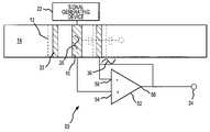
- a through-via 10is formed in an insulating region 12 of a wafer 14 and extends from a front surface 16 to a back surface 18 .
- the through-viacarries a signal 20 from a signal generating device 22 from the front surface to the back surface and to a conductive line 24 or 26 .
- the signalwill not include a DC component.
- the time-varying portion of the signalwill have to drive a parasitic capacitance formed between through-via 10 and surrounding grounded wafer 14 .
- the parasitic capacitanceis an open circuit to any DC voltage, and thus only affects the time-varying portion of the signal including pure AC signals, step functions, transients etc. In practice, the parasitic effect only becomes an issue when trying to sense changes in a capacitance or changes in the charge stored in a capacitor.
- the loading of the signalincreases as the impedance of the signal increases and the impedance of the parasitic capacitance decreases.
- a shielded through-via 30is formed that includes a shield electrode 32 in insulating region 12 around and spaced apart from through-via 10 and a coupling element 34 that couples at least a time-varying portion of signal 20 , and possibly the complete signal, as a signal 36 to shield electrode 32 . If the signal does include a DC component, the DC component may be removed by placing a high pass filter such as a capacitor on either side of the coupling element 34 .
- the coupling elementpreferably has unity gain but a substantial reduction in the effect of the parasitic capacitance can be achieved with a deviation from unity.
- the coupling elementis also preferably characterized by high input impedance so that the coupling element does not load the signal.
- the input impedanceis suitably comparable to the impedance of the signal and preferably higher.
- This parasitic capacitancecan, however, lead to deviations between the through-via and shield electrode voltages.
- other signalscould be coupled to the shield electrode and reflected back through the coupling element to the through-via thereby modulating signal voltage 20 . Therefore the coupling element preferably isolates its input from its output so that changes in shield electrode voltage 36 do not affect signal voltage 20 .
- the other signals that are coupled to the shield electrodecan modulate signal voltage 36 .
- the coupling elementpreferably has low output impedance that creates a virtual AC ground so that the noise coupled through parasitic capacitance 40 to the shield electrode does not affect the coupled signal. A substantial improvement in the parasitic effect can still be realized if the output impedance is not sufficiently small to prevent loading of signal 36 , particularly if the shielded through-via resides in a low noise environment.
- the coupled signal 36is a virtual replica of at least the time-varying portion of input signal 20 in amplitude, frequency and phase but it has a much lower impedance characteristic.
- the coupling elementmay transform the impedance of the signal from 10s of kilo ohms or giga ohms to less than 10 ohms. If the circuit is configured to output coupled signal 36 on conductive line 24 the signal will be far less susceptible to other parasitic capacitances or crosstalk as the signal is routed off the wafer or to another component. The coupling element may induce a small amount of phase delay in the coupled signal.
- the circuitcan be configured to output signal 20 from the through-via directly to conductive line 26 . In most cases it will be preferable to output the low-impedance signal but both options are available.
- the coupling elementis a buffer 50 comprised of a high-gain operational amplifier 52 with feedback.
- Input signal 20is coupled to the non-inverting (+) input 54 .
- Op-amp output 56is feedback to inverting ( ⁇ ) input 58 , which is coupled to shield electrode 32 .
- the bufferprovides unity gain over the signal bandwidth, minimal phase delay, isolation, an input impedance comparable to or larger than the impedance of the signal and an output impedance of typically 0.1-1 ohm.
- the buffered signal 36 applied to shield electrode 32closely tracks complete signal 20 to effectively hold the electric field between the through-via and the shield electrode at zero.
- the insertion of a high pass filter such as a capacitor between the through-via and buffer or buffer and shield electrodewould filter out any DC portion of the signal thereby coupling only the time-varying portion to the shield electrode. Removing the DC portion of the signal improves sensitivity.
- the bufferprovides the isolation and desired impedance characteristics electrically. These same characteristics could be provided optically by an optical isolator that converts electrical signal 20 to an optical signal and than back to coupled electrical signal 36 or mechanically by a MEMS isolator that converts the electrical signal to a mechanical signal and than back to the coupled electrical signal.
- Signal 20 having impedance Zsig 62is input from signal generating device 22 shown in FIG. 1 and establishes a time-varying voltage V(via) across through-via 10 .
- the voltagemay or may not include a DC component, which has no parasitic effect.
- the input impedance Zin 64 of the buffer 50appears in parallel with the impedance Zsig 62 of the signal generating device. Ideally Zin would be infinite but as long as Zin is at least comparable with Zsig and preferably larger, loading of the input signal is usually tolerable.
- the bufferincludes an isolation stage 66 and unity gain stage 68 that replicate signal 20 as signal 36 .
- the buffer's output impedance, hence signal impedance Zout(sig) 70is very small, typically 0.1-1 ohm.
- Buffered signal 36establishes a voltage V(shield) on shield electrode 32 that tracks the voltage V(via) on the through-via.
- V(shield) and V(via)are the voltages on either side of parasitic capacitance 38 formed between shield electrode 32 and through-via 10 as shown in FIGS. 1 and 2 .
- the impedance Zpar 72 of the parasitic capacitance 38does not change, the effect of holding the electric field approximately constant, e.g. zero, is to greatly reduce if not eliminate the effect of the parasitic capacitance.
- noise 74may be coupled back through parasitic capacitance 40 shown in FIG. 1 to the shield electrode 32 .
- the constant electric field and isolation of the bufferprevents these signals from being directly coupled to signal 20 on through-via 10 but they can distort the buffered voltage so that V(shield) does not tightly track V(via).
- the noise 74will induce a current through Zout(sig), which will produce a current that will modulate V(shield). If Zout(sig) is very small, less than 10 ohms for example, the voltage modulation will be negligible. If Zout(sig) is larger, the noise may reduce the shielding effect but a substantial improvement will still be realized.
- buffer signal 36preferably has low impedance Zout(sig) 70 .
- Zout(sig) 70As the signal travels along conductive line 24 it will see other parasitics Zpar 76 . Because signal 36 is no longer actively shielded from these parasitics and other noise sources, the signal's low impedance will minimize the loading and crosstalk effects. For example, the coupling of these parasitics to a 1 or even 10 ohm signal is miniscule compared to the coupling to a 1 mega ohm or gig ohm input signal. In high noise environments, it is more important that the output impedance be low in order to maintain signal quality.
- shield electrode 32is preferably configured to present a constant electric field around and coextensive with the length of the through-via.
- the shield electrodeis configured so that the through-via can ‘see’a portion of the wafer a substantial benefit of the shielded through-via can still be achieved. The goal being to configure the shield electrode to cut-off most if not all of the electric field lines between the wafer and the through-via so that the through-via only sees the constant electric field between itself and the shield electrode.
- a processed wafer 80includes oxide layers 82 on both surfaces and a conformal dielectric coating 84 that defines the insulating region in the wafer, which in this embodiment includes portions of the wafer as well.
- Conductive through-via 86extends from the front to the back surface and is insulated from the wafer by dielectric coating 84 .
- Shield electrode 88is coextensive with the length of through-via 86 and is insulated from both through-via 86 and wafer 80 by the dielectric coating.
- the shield electrodemust be insulated from the wafer otherwise the voltage signal would attempt (and fail) to drive the entire wafer and the coupling element could not drive the shield voltage to effectively track the through-via voltage as desired. If the wafer is resistive (or the shielded through-via is formed in an insulating layer such as a thin-film dielectric or PCB), the shield electrode may contact the surrounding wafer or layer.
- a processed wafer 90includes conformal dielectric coatings 92 and 94 that separate a through-via 96 from a shield electrode 98 and the shield electrode from the wafer.
- the waferis conductive or semi-conductive inner dielectric coating 94 is needed to insulate the shield electrode from the wafer.
- shield electrode 98is substantially but not completely coextensive with the length of through-via 96 but shield electrode 98 wraps around the ends of wafer 90 facing the through-via thereby cutting off electric field lines between the wafer and the through-via.
- a shield electrode 100lies in the insulating region 102 around and spaced apart from a through-via 104 and suitably spaced apart from a surrounding wafer 106 . As shown, the shield electrode completely circumscribes the through-via so that the through-via cannot see any portion of the wafer. Note, the shield electrode does not have to be circular but can take any shape that adequately shields the through-via from the surrounding wafer. As shown in FIG. 5 b , a shield electrode 110 is similarly configured except that it includes a number of small gaps 112 . These gaps may be included, for example, to provide a mechanical fixture to support the inner portion of the insulating region around the through-via.
- the gapsmay occur only near the top and/or bottom of the through-via or could extend the length of the through-via.
- these physical gapsmay appear to be much smaller electrical gaps or may not appear at all, i.e. the field lines from the surrounding wafer terminate on the shield electrode and do not penetrate through to the through-via. Even if some of the electric field lines from the wafer penetrate through to the through-via, a substantial benefit can be achieved from the shielded through-via.
- the shielded through-vias shown in FIGS. 4 a - b and 5 a - b as well as other configurationscan be fabricated using different process flows. For example, a hole may be etched through the entire length of a wafer, followed by a thin dielectric film deposition to provide an isolation region. A conductive layer is deposited to form the shielding electrode, followed by a second thin dielectric film deposition to provide an isolation region between the shield electrode and the via conductor yet to be formed. Next, a second conductive layer is deposited to form the via conductor, which may be a solid piece as depicted in FIGS. 4 and 5 .
- a hole and coaxial annular outer sectionscan be etched through the entire length of a wafer, followed by a thin dielectric film deposition to provide isolation regions.
- a conductive filmis deposited in both the hole and the annular outer sections to form the via conductor and the shielding electrode, respectively, as depicted in FIGS. 4 a and 5 b.
- the shielded through-viacan be used to couple any electrical signal from one side of a layer to another.
- the signalcan be of high or low impedance and can be generated by monolithic circuitry formed in the layer, discrete devices mounted on the layer, devices on another layer, etc.
- the signal on the backside of the layercan be routed via the conductive line to monolithic or discrete circuitry on the layer itself, to circuitry on another wafer in a stack or off of the layer.
- the layercan be a processed wafer formed of conductive, semi-conductive or resistive materials.
- the layercan be an insulating material as would be found in a printed circuit board (PCB) or a passivation stack on a wafer where the stack includes the interconnections for the monolithic circuitry.
- PCBprinted circuit board
- a MEMS sensor 120such as accelerometers, gyroscopes and pressure sensors is formed using conventional MEMS processing techniques on the surface of, for example, a silica wafer 122 .
- the MEMS sensorhas a capacitance of ⁇ 1 pF, hence a very large impedance.
- the sensed signal 124albeit acceleration, rate or pressure is reflected as a small change in this already small capacitance.
- MEMS devices and integrated circuitsare not processed on the same wafer much less the same surface of the same wafer.
- the MEMS wafer 122is stacked on top of an IC wafer 126 that includes monolithic circuits 128 for processing the sensed signal.
- a shield electrode 132is provided in an insulating region 134 (here a conformal dielectric coating) around the through-via and spaced apart from the through-via and silica wafer.
- the through-via and shield electrodeare bonded to metal contact pads 136 and 138 , respectively.
- the buffer shown in FIG. 2is implemented in monolithic circuits 128 to couple signal 124 to the shield electrode to reduce the effect of the parasitic capacitance between through-via 130 and silica wafer 122 . Effective shielding of the parasitic capacitance can improve detection sensitivity of the MEMS sensor by at least one or two orders of magnitude.
- the same or similar shielded through-viacan be placed at multiple via sites throughout the wafer to connect other high-impedance devices through to the IC wafer. It is possible that every through-via may be shielded in this manner or only selected vias. Furthermore, the same or similar shielded through-via can be formed in the IC wafer to carry high (or low) impedance signals to its backside.
- shielded through-vias 140are used to connect metal layers 141 of a multi-layer metal interconnect stack 142 in a thin-film dielectric 144 formed on the surface of a wafer 146 to provide electrical connections for the integrated circuits 148 on the wafer.
- the thin-film dielectric 144 layerprovides the insulating region so the shield electrode 150 need only be spaced apart from the via 152 and not the surrounding layer 144 . Because the layer is itself a dielectric material the effects or parasitic capacitance and isolation are not typically as problematic as with a conductive or semi-conductive wafer. However, as technology advances and the input devices present lower capacitances, e.g. higher impedance, the measurement frequencies increase and circuit densities increase, it may be desirable if not necessary to shield the through-vias.
Landscapes
- Engineering & Computer Science (AREA)
- Microelectronics & Electronic Packaging (AREA)
- Physics & Mathematics (AREA)
- Condensed Matter Physics & Semiconductors (AREA)
- General Physics & Mathematics (AREA)
- Computer Hardware Design (AREA)
- Power Engineering (AREA)
- Electromagnetism (AREA)
- Semiconductor Integrated Circuits (AREA)
Abstract
Description
Claims (22)
Priority Applications (1)
| Application Number | Priority Date | Filing Date | Title |
|---|---|---|---|
| US11/373,223US7589390B2 (en) | 2006-03-10 | 2006-03-10 | Shielded through-via |
Applications Claiming Priority (1)
| Application Number | Priority Date | Filing Date | Title |
|---|---|---|---|
| US11/373,223US7589390B2 (en) | 2006-03-10 | 2006-03-10 | Shielded through-via |
Publications (2)
| Publication Number | Publication Date |
|---|---|
| US20070222021A1 US20070222021A1 (en) | 2007-09-27 |
| US7589390B2true US7589390B2 (en) | 2009-09-15 |
Family
ID=38532466
Family Applications (1)
| Application Number | Title | Priority Date | Filing Date |
|---|---|---|---|
| US11/373,223Expired - Fee RelatedUS7589390B2 (en) | 2006-03-10 | 2006-03-10 | Shielded through-via |
Country Status (1)
| Country | Link |
|---|---|
| US (1) | US7589390B2 (en) |
Cited By (28)
| Publication number | Priority date | Publication date | Assignee | Title |
|---|---|---|---|---|
| US20090130846A1 (en)* | 2007-11-19 | 2009-05-21 | Toshiro Mistuhashi | Semiconductor device fabrication method |
| US20090159322A1 (en)* | 2007-12-21 | 2009-06-25 | Industrial Technology Research Institute | Through hole capacitor and method of manufacturing the same |
| US20090201654A1 (en)* | 2008-02-08 | 2009-08-13 | Lambert Simonovich | Method and system for improving electrical performance of vias for high data rate transmission |
| US20090224376A1 (en)* | 2008-03-07 | 2009-09-10 | Choi Bok Kyu | Circuit board having conductive shield member and semiconductor package using the same |
| US20100140749A1 (en)* | 2008-12-08 | 2010-06-10 | Chien-Li Kuo | Semiconductor device |
| US20100230822A1 (en)* | 2009-03-13 | 2010-09-16 | Stats Chippac, Ltd. | Semiconductor Die and Method of Forming Noise Absorbing Regions Between THVS in Peripheral Region of the Die |
| US20110005814A1 (en)* | 2009-07-10 | 2011-01-13 | Inventec Appliances (Shanghai) Co., Ltd. | Circuit board via structure and method forming the same |
| KR101078744B1 (en) | 2010-05-06 | 2011-11-02 | 주식회사 하이닉스반도체 | Laminated Semiconductor Packages |
| CN102598261A (en)* | 2009-10-27 | 2012-07-18 | 吉林克斯公司 | High impedance electrical connection via |
| US8492260B2 (en) | 2010-08-30 | 2013-07-23 | Semionductor Components Industries, LLC | Processes of forming an electronic device including a feature in a trench |
| US8981533B2 (en) | 2012-09-13 | 2015-03-17 | Semiconductor Components Industries, Llc | Electronic device including a via and a conductive structure, a process of forming the same, and an interposer |
| CN104735907A (en)* | 2013-12-20 | 2015-06-24 | 财团法人工业技术研究院 | circuit board with transmission hole and manufacturing method thereof |
| US9343393B2 (en) | 2012-08-15 | 2016-05-17 | Industrial Technology Research Institute | Semiconductor substrate assembly with embedded resistance element |
| CN105684145A (en)* | 2013-08-08 | 2016-06-15 | 伊文萨思公司 | Ultra high performance interposer |
| US9391049B2 (en) | 2013-12-30 | 2016-07-12 | Industrial Technology Research Institute | Molding package assembly and molding material |
| WO2017079424A1 (en)* | 2015-11-05 | 2017-05-11 | Massachusetts Institute Of Technology | Shielded through via structures and methods for fabricating shielded through via structures |
| US9769398B2 (en) | 2016-01-06 | 2017-09-19 | Microsoft Technology Licensing, Llc | Image sensor with large-area global shutter contact |
| US9780075B2 (en) | 2014-08-11 | 2017-10-03 | Massachusetts Institute Of Technology | Interconnect structures for assembly of multi-layer semiconductor devices |
| US9786633B2 (en) | 2014-04-23 | 2017-10-10 | Massachusetts Institute Of Technology | Interconnect structures for fine pitch assembly of semiconductor structures and related techniques |
| US9812429B2 (en) | 2014-11-05 | 2017-11-07 | Massachusetts Institute Of Technology | Interconnect structures for assembly of multi-layer semiconductor devices |
| US9812354B2 (en) | 2015-05-15 | 2017-11-07 | Semiconductor Components Industries, Llc | Process of forming an electronic device including a material defining a void |
| US9900985B2 (en) | 2016-01-29 | 2018-02-20 | Keysight Technologies, Inc. | Three-dimensional interconnect structure adapted for high frequency RF circuits |
| US10134972B2 (en) | 2015-07-23 | 2018-11-20 | Massachusetts Institute Of Technology | Qubit and coupler circuit structures and coupling techniques |
| US10242968B2 (en) | 2015-11-05 | 2019-03-26 | Massachusetts Institute Of Technology | Interconnect structure and semiconductor structures for assembly of cryogenic electronic packages |
| US10381541B2 (en) | 2016-10-11 | 2019-08-13 | Massachusetts Institute Of Technology | Cryogenic electronic packages and methods for fabricating cryogenic electronic packages |
| US10658424B2 (en) | 2015-07-23 | 2020-05-19 | Massachusetts Institute Of Technology | Superconducting integrated circuit |
| US10769546B1 (en) | 2015-04-27 | 2020-09-08 | Rigetti & Co, Inc. | Microwave integrated quantum circuits with cap wafer and methods for making the same |
| US11770982B1 (en) | 2017-06-19 | 2023-09-26 | Rigetti & Co, Llc | Microwave integrated quantum circuits with cap wafers and their methods of manufacture |
Families Citing this family (35)
| Publication number | Priority date | Publication date | Assignee | Title |
|---|---|---|---|---|
| KR101031134B1 (en)* | 2008-09-11 | 2011-04-27 | 주식회사 동부하이텍 | Contact of semiconductor device and manufacturing method thereof |
| US8710599B2 (en)* | 2009-08-04 | 2014-04-29 | Fairchild Semiconductor Corporation | Micromachined devices and fabricating the same |
| US20110241185A1 (en)* | 2010-04-05 | 2011-10-06 | International Business Machines Corporation | Signal shielding through-substrate vias for 3d integration |
| US20110291287A1 (en)* | 2010-05-25 | 2011-12-01 | Xilinx, Inc. | Through-silicon vias with low parasitic capacitance |
| WO2012037536A2 (en) | 2010-09-18 | 2012-03-22 | Fairchild Semiconductor Corporation | Packaging to reduce stress on microelectromechanical systems |
| CN103221778B (en) | 2010-09-18 | 2016-03-30 | 快捷半导体公司 | There is single micromechanics one chip three-axis gyroscope driven |
| US9095072B2 (en) | 2010-09-18 | 2015-07-28 | Fairchild Semiconductor Corporation | Multi-die MEMS package |
| CN103221779B (en) | 2010-09-18 | 2017-05-31 | 快捷半导体公司 | The axle inertial sensor of micromechanics monoblock type six |
| KR101443730B1 (en) | 2010-09-18 | 2014-09-23 | 페어차일드 세미컨덕터 코포레이션 | A microelectromechanical die, and a method for making a low-quadrature-error suspension |
| US9278845B2 (en) | 2010-09-18 | 2016-03-08 | Fairchild Semiconductor Corporation | MEMS multi-axis gyroscope Z-axis electrode structure |
| WO2012040211A2 (en) | 2010-09-20 | 2012-03-29 | Fairchild Semiconductor Corporation | Microelectromechanical pressure sensor including reference capacitor |
| WO2012040245A2 (en) | 2010-09-20 | 2012-03-29 | Fairchild Semiconductor Corporation | Through silicon via with reduced shunt capacitance |
| US9013615B2 (en) | 2011-09-21 | 2015-04-21 | Semiconductor Components Industries, Llc | Image sensor with flexible interconnect capabilities |
| US9062972B2 (en) | 2012-01-31 | 2015-06-23 | Fairchild Semiconductor Corporation | MEMS multi-axis accelerometer electrode structure |
| US8978475B2 (en) | 2012-02-01 | 2015-03-17 | Fairchild Semiconductor Corporation | MEMS proof mass with split z-axis portions |
| US8754694B2 (en) | 2012-04-03 | 2014-06-17 | Fairchild Semiconductor Corporation | Accurate ninety-degree phase shifter |
| US8742964B2 (en) | 2012-04-04 | 2014-06-03 | Fairchild Semiconductor Corporation | Noise reduction method with chopping for a merged MEMS accelerometer sensor |
| US9488693B2 (en) | 2012-04-04 | 2016-11-08 | Fairchild Semiconductor Corporation | Self test of MEMS accelerometer with ASICS integrated capacitors |
| EP2647952B1 (en) | 2012-04-05 | 2017-11-15 | Fairchild Semiconductor Corporation | Mems device automatic-gain control loop for mechanical amplitude drive |
| US9069006B2 (en) | 2012-04-05 | 2015-06-30 | Fairchild Semiconductor Corporation | Self test of MEMS gyroscope with ASICs integrated capacitors |
| KR102058489B1 (en) | 2012-04-05 | 2019-12-23 | 페어차일드 세미컨덕터 코포레이션 | Mems device front-end charge amplifier |
| EP2647955B8 (en) | 2012-04-05 | 2018-12-19 | Fairchild Semiconductor Corporation | MEMS device quadrature phase shift cancellation |
| US9094027B2 (en) | 2012-04-12 | 2015-07-28 | Fairchild Semiconductor Corporation | Micro-electro-mechanical-system (MEMS) driver |
| US9625272B2 (en) | 2012-04-12 | 2017-04-18 | Fairchild Semiconductor Corporation | MEMS quadrature cancellation and signal demodulation |
| DE102013014881B4 (en) | 2012-09-12 | 2023-05-04 | Fairchild Semiconductor Corporation | Enhanced silicon via with multi-material fill |
| US20140111496A1 (en)* | 2012-10-22 | 2014-04-24 | Apple Inc. | Displays with Circuitry for Compensating Parasitic Coupling Effects |
| FR3005763B1 (en) | 2013-05-17 | 2016-10-14 | Fogale Nanotech | DEVICE AND METHOD FOR A CAPACITIVE CONTROL INTERFACE ADAPTED TO THE IMPLEMENTATION OF ELECTRODES OF HIGHLY RESISTIVE MEASUREMENTS |
| US9123738B1 (en) | 2014-05-16 | 2015-09-01 | Xilinx, Inc. | Transmission line via structure |
| FR3028061B1 (en)* | 2014-10-29 | 2016-12-30 | Fogale Nanotech | CAPACITIVE SENSOR DEVICE COMPRISING ADJUSTED ELECTRODES |
| FR3032287B1 (en) | 2015-02-04 | 2018-03-09 | Quickstep Technologies Llc | MULTILAYER CAPACITIVE DETECTION DEVICE, AND APPARATUS COMPRISING THE DEVICE |
| US10490483B2 (en)* | 2016-03-07 | 2019-11-26 | Micron Technology, Inc. | Low capacitance through substrate via structures |
| US10607885B2 (en)* | 2016-03-30 | 2020-03-31 | Intel Corporation | Shell structure for insulation of a through-substrate interconnect |
| WO2018093275A1 (en)* | 2016-11-17 | 2018-05-24 | Stretchsense Limited | A stretch sensor with an improved flexible interconnect |
| WO2019004991A1 (en)* | 2017-06-25 | 2019-01-03 | Intel Corporation | Quantum computing assemblies |
| EP4296621A1 (en)* | 2022-06-23 | 2023-12-27 | TE Connectivity Sensors France | Capacitive sensor device |
Citations (16)
| Publication number | Priority date | Publication date | Assignee | Title |
|---|---|---|---|---|
| US4348253A (en) | 1981-11-12 | 1982-09-07 | Rca Corporation | Method for fabricating via holes in a semiconductor wafer |
| US4445978A (en) | 1983-03-09 | 1984-05-01 | Rca Corporation | Method for fabricating via connectors through semiconductor wafers |
| US5170081A (en)* | 1991-01-31 | 1992-12-08 | Pioneer Electronic Corporation | Ground isolation circuit |
| US5949030A (en) | 1997-11-14 | 1999-09-07 | International Business Machines Corporation | Vias and method for making the same in organic board and chip carriers |
| US6151967A (en)* | 1998-03-10 | 2000-11-28 | Horizon Technology Group | Wide dynamic range capacitive transducer |
| US6221769B1 (en) | 1999-03-05 | 2001-04-24 | International Business Machines Corporation | Method for integrated circuit power and electrical connections via through-wafer interconnects |
| US6589594B1 (en) | 2000-08-31 | 2003-07-08 | Micron Technology, Inc. | Method for filling a wafer through-via with a conductive material |
| US6645832B2 (en) | 2002-02-20 | 2003-11-11 | Intel Corporation | Etch stop layer for silicon (Si) via etch in three-dimensional (3-D) wafer-to-wafer vertical stack |
| US6661085B2 (en) | 2002-02-06 | 2003-12-09 | Intel Corporation | Barrier structure against corrosion and contamination in three-dimensional (3-D) wafer-to-wafer vertical stack |
| US6717071B2 (en) | 2000-08-11 | 2004-04-06 | Industrial Technology Research Institute | Coaxial via hole and process of fabricating the same |
| US6762076B2 (en) | 2002-02-20 | 2004-07-13 | Intel Corporation | Process of vertically stacking multiple wafers supporting different active integrated circuit (IC) devices |
| US20040188826A1 (en)* | 2003-03-31 | 2004-09-30 | Palanduz Cengiz A. | Interposer with signal and power supply through vias |
| US6821826B1 (en) | 2003-09-30 | 2004-11-23 | International Business Machines Corporation | Three dimensional CMOS integrated circuits having device layers built on different crystal oriented wafers |
| US6852927B2 (en) | 2001-10-18 | 2005-02-08 | Nec Schott Components Corporation | Thin metal package and manufacturing method thereof |
| US6852627B2 (en) | 2003-03-05 | 2005-02-08 | Micron Technology, Inc. | Conductive through wafer vias |
| US20050046480A1 (en)* | 2003-08-26 | 2005-03-03 | Dyer Kenneth C. | Common mode feedback circuit for fully differential two-stage operational amplifiers |
Family Cites Families (1)
| Publication number | Priority date | Publication date | Assignee | Title |
|---|---|---|---|---|
| US6672076B2 (en)* | 2001-02-09 | 2004-01-06 | Bsst Llc | Efficiency thermoelectrics utilizing convective heat flow |
- 2006
- 2006-03-10USUS11/373,223patent/US7589390B2/ennot_activeExpired - Fee Related
Patent Citations (17)
| Publication number | Priority date | Publication date | Assignee | Title |
|---|---|---|---|---|
| US4348253A (en) | 1981-11-12 | 1982-09-07 | Rca Corporation | Method for fabricating via holes in a semiconductor wafer |
| US4445978A (en) | 1983-03-09 | 1984-05-01 | Rca Corporation | Method for fabricating via connectors through semiconductor wafers |
| US5170081A (en)* | 1991-01-31 | 1992-12-08 | Pioneer Electronic Corporation | Ground isolation circuit |
| US5949030A (en) | 1997-11-14 | 1999-09-07 | International Business Machines Corporation | Vias and method for making the same in organic board and chip carriers |
| US6151967A (en)* | 1998-03-10 | 2000-11-28 | Horizon Technology Group | Wide dynamic range capacitive transducer |
| US6221769B1 (en) | 1999-03-05 | 2001-04-24 | International Business Machines Corporation | Method for integrated circuit power and electrical connections via through-wafer interconnects |
| US20040149490A1 (en)* | 2000-08-11 | 2004-08-05 | Huey-Ru Chang | Coaxial via hole and process of fabricating the same |
| US6717071B2 (en) | 2000-08-11 | 2004-04-06 | Industrial Technology Research Institute | Coaxial via hole and process of fabricating the same |
| US6589594B1 (en) | 2000-08-31 | 2003-07-08 | Micron Technology, Inc. | Method for filling a wafer through-via with a conductive material |
| US6852927B2 (en) | 2001-10-18 | 2005-02-08 | Nec Schott Components Corporation | Thin metal package and manufacturing method thereof |
| US6661085B2 (en) | 2002-02-06 | 2003-12-09 | Intel Corporation | Barrier structure against corrosion and contamination in three-dimensional (3-D) wafer-to-wafer vertical stack |
| US6762076B2 (en) | 2002-02-20 | 2004-07-13 | Intel Corporation | Process of vertically stacking multiple wafers supporting different active integrated circuit (IC) devices |
| US6645832B2 (en) | 2002-02-20 | 2003-11-11 | Intel Corporation | Etch stop layer for silicon (Si) via etch in three-dimensional (3-D) wafer-to-wafer vertical stack |
| US6852627B2 (en) | 2003-03-05 | 2005-02-08 | Micron Technology, Inc. | Conductive through wafer vias |
| US20040188826A1 (en)* | 2003-03-31 | 2004-09-30 | Palanduz Cengiz A. | Interposer with signal and power supply through vias |
| US20050046480A1 (en)* | 2003-08-26 | 2005-03-03 | Dyer Kenneth C. | Common mode feedback circuit for fully differential two-stage operational amplifiers |
| US6821826B1 (en) | 2003-09-30 | 2004-11-23 | International Business Machines Corporation | Three dimensional CMOS integrated circuits having device layers built on different crystal oriented wafers |
Non-Patent Citations (1)
| Title |
|---|
| Chang et al. "A CMOS Differential Buffer Amplifier with Accurate Gain and Clipping Control." IEEE Journal of Solid-State Circuits, vol. 30, No.7, Jul. 1995, p. 731.* |
Cited By (54)
| Publication number | Priority date | Publication date | Assignee | Title |
|---|---|---|---|---|
| US20090130846A1 (en)* | 2007-11-19 | 2009-05-21 | Toshiro Mistuhashi | Semiconductor device fabrication method |
| US7906431B2 (en)* | 2007-11-19 | 2011-03-15 | Oki Semiconductor Co., Ltd. | Semiconductor device fabrication method |
| US7894178B2 (en)* | 2007-12-21 | 2011-02-22 | Industrial Technology Research Institute | Through hole capacitor and method of manufacturing the same |
| US20090159322A1 (en)* | 2007-12-21 | 2009-06-25 | Industrial Technology Research Institute | Through hole capacitor and method of manufacturing the same |
| US20090201654A1 (en)* | 2008-02-08 | 2009-08-13 | Lambert Simonovich | Method and system for improving electrical performance of vias for high data rate transmission |
| US8084839B2 (en) | 2008-03-07 | 2011-12-27 | Hynix Semiconductor Inc. | Circuit board having conductive shield member and semiconductor package using the same |
| US20100321900A1 (en)* | 2008-03-07 | 2010-12-23 | Hynix Semiconductor Inc. | Circuit board having conductive shield member and semiconductor package using the same |
| US20090224376A1 (en)* | 2008-03-07 | 2009-09-10 | Choi Bok Kyu | Circuit board having conductive shield member and semiconductor package using the same |
| US7808072B2 (en)* | 2008-03-07 | 2010-10-05 | Hynix Semiconductor Inc. | Circuit board having conductive shield member and semiconductor package using the same |
| US20120261834A1 (en)* | 2008-12-08 | 2012-10-18 | Chien-Li Kuo | Semiconductor device |
| US20100140749A1 (en)* | 2008-12-08 | 2010-06-10 | Chien-Li Kuo | Semiconductor device |
| US8227889B2 (en)* | 2008-12-08 | 2012-07-24 | United Microelectronics Corp. | Semiconductor device |
| US20100230822A1 (en)* | 2009-03-13 | 2010-09-16 | Stats Chippac, Ltd. | Semiconductor Die and Method of Forming Noise Absorbing Regions Between THVS in Peripheral Region of the Die |
| US9236352B2 (en) | 2009-03-13 | 2016-01-12 | Stats Chippac, Ltd. | Semiconductor die and method of forming noise absorbing regions between THVs in peripheral region of the die |
| US8093151B2 (en)* | 2009-03-13 | 2012-01-10 | Stats Chippac, Ltd. | Semiconductor die and method of forming noise absorbing regions between THVS in peripheral region of the die |
| US20110005814A1 (en)* | 2009-07-10 | 2011-01-13 | Inventec Appliances (Shanghai) Co., Ltd. | Circuit board via structure and method forming the same |
| CN102598261A (en)* | 2009-10-27 | 2012-07-18 | 吉林克斯公司 | High impedance electrical connection via |
| CN102598261B (en)* | 2009-10-27 | 2014-09-17 | 吉林克斯公司 | High impedance electrical connection via |
| US8525319B2 (en) | 2010-05-06 | 2013-09-03 | SK Hynix Inc. | Selecting chips within a stacked semiconductor package using through-electrodes |
| KR101078744B1 (en) | 2010-05-06 | 2011-11-02 | 주식회사 하이닉스반도체 | Laminated Semiconductor Packages |
| US8492260B2 (en) | 2010-08-30 | 2013-07-23 | Semionductor Components Industries, LLC | Processes of forming an electronic device including a feature in a trench |
| US9117802B2 (en) | 2010-08-30 | 2015-08-25 | Semiconductor Components Industries, Llc | Electronic device including a feature in an opening |
| US9343393B2 (en) | 2012-08-15 | 2016-05-17 | Industrial Technology Research Institute | Semiconductor substrate assembly with embedded resistance element |
| US8981533B2 (en) | 2012-09-13 | 2015-03-17 | Semiconductor Components Industries, Llc | Electronic device including a via and a conductive structure, a process of forming the same, and an interposer |
| CN105684145A (en)* | 2013-08-08 | 2016-06-15 | 伊文萨思公司 | Ultra high performance interposer |
| CN105684145B (en)* | 2013-08-08 | 2019-04-05 | 伊文萨思公司 | Ultra High Performance Interpolator |
| US9125304B2 (en) | 2013-12-20 | 2015-09-01 | Industrial Technology Research Institute | Circuit board having via and manufacturing method thereof |
| CN104735907A (en)* | 2013-12-20 | 2015-06-24 | 财团法人工业技术研究院 | circuit board with transmission hole and manufacturing method thereof |
| US9258883B2 (en)* | 2013-12-20 | 2016-02-09 | Industrial Technology Research Institute | Via structure |
| CN104735907B (en)* | 2013-12-20 | 2017-12-22 | 财团法人工业技术研究院 | Circuit board with transmission holes and manufacturing method thereof |
| US9391049B2 (en) | 2013-12-30 | 2016-07-12 | Industrial Technology Research Institute | Molding package assembly and molding material |
| US9786633B2 (en) | 2014-04-23 | 2017-10-10 | Massachusetts Institute Of Technology | Interconnect structures for fine pitch assembly of semiconductor structures and related techniques |
| US9780075B2 (en) | 2014-08-11 | 2017-10-03 | Massachusetts Institute Of Technology | Interconnect structures for assembly of multi-layer semiconductor devices |
| US10418350B2 (en) | 2014-08-11 | 2019-09-17 | Massachusetts Institute Of Technology | Semiconductor structures for assembly in multi-layer semiconductor devices including at least one semiconductor structure |
| US10079224B2 (en) | 2014-08-11 | 2018-09-18 | Massachusetts Institute Of Technology | Interconnect structures for assembly of semiconductor structures including at least one integrated circuit structure |
| US10229897B2 (en) | 2014-08-11 | 2019-03-12 | Massachusetts Institute Of Technology | Multi-layer semiconductor structure and methods for fabricating multi-layer semiconductor structures |
| US9812429B2 (en) | 2014-11-05 | 2017-11-07 | Massachusetts Institute Of Technology | Interconnect structures for assembly of multi-layer semiconductor devices |
| US9881904B2 (en) | 2014-11-05 | 2018-01-30 | Massachusetts Institute Of Technology | Multi-layer semiconductor devices fabricated using a combination of substrate and via structures and fabrication techniques |
| US11574230B1 (en) | 2015-04-27 | 2023-02-07 | Rigetti & Co, Llc | Microwave integrated quantum circuits with vias and methods for making the same |
| US10769546B1 (en) | 2015-04-27 | 2020-09-08 | Rigetti & Co, Inc. | Microwave integrated quantum circuits with cap wafer and methods for making the same |
| US9812354B2 (en) | 2015-05-15 | 2017-11-07 | Semiconductor Components Industries, Llc | Process of forming an electronic device including a material defining a void |
| US10658424B2 (en) | 2015-07-23 | 2020-05-19 | Massachusetts Institute Of Technology | Superconducting integrated circuit |
| US10134972B2 (en) | 2015-07-23 | 2018-11-20 | Massachusetts Institute Of Technology | Qubit and coupler circuit structures and coupling techniques |
| US10121754B2 (en) | 2015-11-05 | 2018-11-06 | Massachusetts Institute Of Technology | Interconnect structures and methods for fabricating interconnect structures |
| US10242968B2 (en) | 2015-11-05 | 2019-03-26 | Massachusetts Institute Of Technology | Interconnect structure and semiconductor structures for assembly of cryogenic electronic packages |
| US10396269B2 (en) | 2015-11-05 | 2019-08-27 | Massachusetts Institute Of Technology | Interconnect structures for assembly of semiconductor structures including superconducting integrated circuits |
| US10199553B1 (en) | 2015-11-05 | 2019-02-05 | Massachusetts Institute Of Technology | Shielded through via structures and methods for fabricating shielded through via structures |
| WO2017079424A1 (en)* | 2015-11-05 | 2017-05-11 | Massachusetts Institute Of Technology | Shielded through via structures and methods for fabricating shielded through via structures |
| US9769398B2 (en) | 2016-01-06 | 2017-09-19 | Microsoft Technology Licensing, Llc | Image sensor with large-area global shutter contact |
| US9900985B2 (en) | 2016-01-29 | 2018-02-20 | Keysight Technologies, Inc. | Three-dimensional interconnect structure adapted for high frequency RF circuits |
| US10381541B2 (en) | 2016-10-11 | 2019-08-13 | Massachusetts Institute Of Technology | Cryogenic electronic packages and methods for fabricating cryogenic electronic packages |
| US10586909B2 (en) | 2016-10-11 | 2020-03-10 | Massachusetts Institute Of Technology | Cryogenic electronic packages and assemblies |
| US11770982B1 (en) | 2017-06-19 | 2023-09-26 | Rigetti & Co, Llc | Microwave integrated quantum circuits with cap wafers and their methods of manufacture |
| US12207569B1 (en) | 2017-06-19 | 2025-01-21 | Rigetti & Co, Llc | Microwave integrated quantum circuits with cap wafers and their methods of manufacture |
Also Published As
| Publication number | Publication date |
|---|---|
| US20070222021A1 (en) | 2007-09-27 |
Similar Documents
| Publication | Publication Date | Title |
|---|---|---|
| US7589390B2 (en) | Shielded through-via | |
| CN101174611B (en) | Multi-ground shielding semiconductor package, method of fabricating the package, and method of preventing noise using multi-ground shielding | |
| KR100427111B1 (en) | Energy conditioning circuit assembly | |
| US7649499B2 (en) | High-frequency module | |
| US6373348B1 (en) | High speed differential attenuator using a low temperature co-fired ceramic substrate | |
| US20110284262A1 (en) | Controlled Self Assembly of Anisotropic Conductive Adhesives Based on Ferromagnetic Particles | |
| US11937368B2 (en) | Structure for circuit interconnects | |
| JP5327216B2 (en) | High frequency substrate and high frequency module | |
| US10453774B1 (en) | Thermally enhanced substrate | |
| CN100505178C (en) | Through substrate, interposer, and through substrate manufacturing method | |
| WO2011145269A1 (en) | Ic current measurement device and ic current measurement adapter | |
| US11678433B2 (en) | Printed circuit board assembly for edge-coupling to an integrated circuit | |
| KR100663265B1 (en) | Multilayer substrate and its manufacturing method | |
| US6998292B2 (en) | Apparatus and method for inter-chip or chip-to-substrate connection with a sub-carrier | |
| US7170361B1 (en) | Method and apparatus of interposing voltage reference traces between signal traces in semiconductor devices | |
| US11412610B2 (en) | Apparatus, system, and method for mitigating the swiss cheese effect in high-current circuit boards | |
| TWI621194B (en) | Testing board component | |
| WO2022241815A1 (en) | Preparation and encapsulation process for high-stopband rejection low-pass filter for 5g communications | |
| US10667385B2 (en) | Impedance control using anti-pad geometries | |
| JP2004112143A (en) | Connecting structure of conductor for high frequency signal and semiconductor integrated circuit package | |
| JP2023531696A (en) | solder column grid array capacitor | |
| US20210391633A1 (en) | Integrated circulator system | |
| US12349267B1 (en) | Apparatus, system, and method for achieving certain characteristics in stacked vias formed through multilaminate circuit boards | |
| Schmueckle et al. | A 77 GHz broadband flip-chip transition on LTCC submount | |
| WO2018042518A1 (en) | Semiconductor device and printed circuit board |
Legal Events
| Date | Code | Title | Description |
|---|---|---|---|
| AS | Assignment | Owner name:ROCKWELL SCIENTIFIC LICENSING LLC, CALIFORNIA Free format text:ASSIGNMENT OF ASSIGNORS INTEREST;ASSIGNOR:YAO, JUN JASON;REEL/FRAME:017674/0994 Effective date:20060309 | |
| AS | Assignment | Owner name:TELEDYNE LICENSING, LLC, CALIFORNIA Free format text:CHANGE OF NAME;ASSIGNOR:ROCKWELL SCIENTIFIC LICENSING, LLC;REEL/FRAME:018583/0159 Effective date:20060918 Owner name:TELEDYNE LICENSING, LLC,CALIFORNIA Free format text:CHANGE OF NAME;ASSIGNOR:ROCKWELL SCIENTIFIC LICENSING, LLC;REEL/FRAME:018583/0159 Effective date:20060918 | |
| STCF | Information on status: patent grant | Free format text:PATENTED CASE | |
| CC | Certificate of correction | ||
| AS | Assignment | Owner name:TELEDYNE SCIENTIFIC & IMAGING, LLC, CALIFORNIA Free format text:MERGER;ASSIGNOR:TELEDYNE LICENSING, LLP;REEL/FRAME:027636/0298 Effective date:20111221 | |
| AS | Assignment | Owner name:TELEDYNE SCIENTIFIC & IMAGING, LLC, CALIFORNIA Free format text:CORRECTIVE ASSIGNMENT TO CORRECT THE CONVEYING PARTY AS TELEDYNE LICENSING, LLC AND NOT TELEDYNE LICENSING, LLP PREVIOUSLY RECORDED ON REEL 027636 FRAME 0298. ASSIGNOR(S) HEREBY CONFIRMS THE MERGER;ASSIGNOR:TELEDYNE LICENSING, LLC;REEL/FRAME:027677/0720 Effective date:20111221 | |
| FPAY | Fee payment | Year of fee payment:4 | |
| FPAY | Fee payment | Year of fee payment:8 | |
| FEPP | Fee payment procedure | Free format text:MAINTENANCE FEE REMINDER MAILED (ORIGINAL EVENT CODE: REM.); ENTITY STATUS OF PATENT OWNER: LARGE ENTITY | |
| LAPS | Lapse for failure to pay maintenance fees | Free format text:PATENT EXPIRED FOR FAILURE TO PAY MAINTENANCE FEES (ORIGINAL EVENT CODE: EXP.); ENTITY STATUS OF PATENT OWNER: LARGE ENTITY | |
| STCH | Information on status: patent discontinuation | Free format text:PATENT EXPIRED DUE TO NONPAYMENT OF MAINTENANCE FEES UNDER 37 CFR 1.362 | |
| FP | Lapsed due to failure to pay maintenance fee | Effective date:20210915 |