US7589380B2 - Method for forming integrated circuit utilizing dual semiconductors - Google Patents
Method for forming integrated circuit utilizing dual semiconductorsDownload PDFInfo
- Publication number
- US7589380B2 US7589380B2US11/220,942US22094205AUS7589380B2US 7589380 B2US7589380 B2US 7589380B2US 22094205 AUS22094205 AUS 22094205AUS 7589380 B2US7589380 B2US 7589380B2
- Authority
- US
- United States
- Prior art keywords
- layer
- transistor
- semiconductor layer
- germanium
- integrated circuit
- Prior art date
- Legal status (The legal status is an assumption and is not a legal conclusion. Google has not performed a legal analysis and makes no representation as to the accuracy of the status listed.)
- Active, expires
Links
- 239000004065semiconductorSubstances0.000titleclaimsabstractdescription75
- 238000000034methodMethods0.000titledescription23
- 230000009977dual effectEffects0.000title1
- GNPVGFCGXDBREM-UHFFFAOYSA-Ngermanium atomChemical compound[Ge]GNPVGFCGXDBREM-UHFFFAOYSA-N0.000claimsdescription77
- 229910052732germaniumInorganic materials0.000claimsdescription66
- 229910052710siliconInorganic materials0.000claimsdescription44
- 239000010703siliconSubstances0.000claimsdescription44
- 239000013078crystalSubstances0.000claimsdescription19
- 238000012545processingMethods0.000claimsdescription13
- 239000000463materialSubstances0.000claimsdescription12
- 229910000927Ge alloyInorganic materials0.000claims1
- 239000010410layerSubstances0.000description54
- XUIMIQQOPSSXEZ-UHFFFAOYSA-NSiliconChemical compound[Si]XUIMIQQOPSSXEZ-UHFFFAOYSA-N0.000description41
- 239000000758substrateSubstances0.000description23
- 230000015572biosynthetic processEffects0.000description6
- 239000002184metalSubstances0.000description6
- 229910021420polycrystalline siliconInorganic materials0.000description6
- 229920005591polysiliconPolymers0.000description6
- 239000012212insulatorSubstances0.000description4
- 229910000577Silicon-germaniumInorganic materials0.000description3
- LEVVHYCKPQWKOP-UHFFFAOYSA-N[Si].[Ge]Chemical compound[Si].[Ge]LEVVHYCKPQWKOP-UHFFFAOYSA-N0.000description3
- 239000000969carrierSubstances0.000description3
- 238000000407epitaxyMethods0.000description3
- 238000002955isolationMethods0.000description3
- 208000012868OvergrowthDiseases0.000description2
- 238000013459approachMethods0.000description2
- 230000007547defectEffects0.000description2
- 238000000151depositionMethods0.000description2
- 238000005516engineering processMethods0.000description2
- 238000004943liquid phase epitaxyMethods0.000description2
- 229910021421monocrystalline siliconInorganic materials0.000description2
- 230000006978adaptationEffects0.000description1
- 239000000654additiveSubstances0.000description1
- 230000000996additive effectEffects0.000description1
- 230000002411adverseEffects0.000description1
- 229910045601alloyInorganic materials0.000description1
- 239000000956alloySubstances0.000description1
- 230000004075alterationEffects0.000description1
- 238000010276constructionMethods0.000description1
- 230000003247decreasing effectEffects0.000description1
- 230000002950deficientEffects0.000description1
- 230000008021depositionEffects0.000description1
- 239000003989dielectric materialSubstances0.000description1
- 238000005530etchingMethods0.000description1
- 238000004880explosionMethods0.000description1
- 230000005669field effectEffects0.000description1
- 239000007943implantSubstances0.000description1
- 239000011229interlayerSubstances0.000description1
- 238000001459lithographyMethods0.000description1
- 238000012856packingMethods0.000description1
- 238000011160researchMethods0.000description1
- HBMJWWWQQXIZIP-UHFFFAOYSA-Nsilicon carbideChemical compound[Si+]#[C-]HBMJWWWQQXIZIP-UHFFFAOYSA-N0.000description1
- 229910010271silicon carbideInorganic materials0.000description1
- 238000012995silicone-based technologyMethods0.000description1
- 239000000126substanceSubstances0.000description1
Images


Classifications
- H—ELECTRICITY
- H10—SEMICONDUCTOR DEVICES; ELECTRIC SOLID-STATE DEVICES NOT OTHERWISE PROVIDED FOR
- H10D—INORGANIC ELECTRIC SEMICONDUCTOR DEVICES
- H10D30/00—Field-effect transistors [FET]
- H10D30/60—Insulated-gate field-effect transistors [IGFET]
- H—ELECTRICITY
- H10—SEMICONDUCTOR DEVICES; ELECTRIC SOLID-STATE DEVICES NOT OTHERWISE PROVIDED FOR
- H10D—INORGANIC ELECTRIC SEMICONDUCTOR DEVICES
- H10D84/00—Integrated devices formed in or on semiconductor substrates that comprise only semiconducting layers, e.g. on Si wafers or on GaAs-on-Si wafers
- H10D84/01—Manufacture or treatment
- H10D84/02—Manufacture or treatment characterised by using material-based technologies
- H10D84/03—Manufacture or treatment characterised by using material-based technologies using Group IV technology, e.g. silicon technology or silicon-carbide [SiC] technology
- H10D84/038—Manufacture or treatment characterised by using material-based technologies using Group IV technology, e.g. silicon technology or silicon-carbide [SiC] technology using silicon technology, e.g. SiGe
- H—ELECTRICITY
- H10—SEMICONDUCTOR DEVICES; ELECTRIC SOLID-STATE DEVICES NOT OTHERWISE PROVIDED FOR
- H10D—INORGANIC ELECTRIC SEMICONDUCTOR DEVICES
- H10D88/00—Three-dimensional [3D] integrated devices
- H—ELECTRICITY
- H10—SEMICONDUCTOR DEVICES; ELECTRIC SOLID-STATE DEVICES NOT OTHERWISE PROVIDED FOR
- H10D—INORGANIC ELECTRIC SEMICONDUCTOR DEVICES
- H10D88/00—Three-dimensional [3D] integrated devices
- H10D88/01—Manufacture or treatment
Definitions
- the present inventionrelates generally to methods for forming integrated electronic circuits, and in particular, to methods for forming MOS circuits using plural overlapping layers of different semiconductor materials.
- Silicon integrated circuits “IC's”are ubiquitous in modern electronics. These integrated electronic circuits, which contain up to millions of transistors, can be formed simultaneously by a series of process steps using masks containing millions of features. Silicon IC technology has led to an explosion of such electronic devices as computers, handheld telephones, portable music and movie players.
- Straincan be introduced by a variety of processing techniques, such as the deposition of dielectric layers with high intrinsic strain, or the growth of silicon layers on a template material which has a different lattice constant, such as silicon-germanium. By judicious choice of materials, a particular strain state can be built into a transistor and can enhance the mobility of carriers therein.
- An alternative approachuses different crystal orientations to optimize the mobility of holes and electrons separately. By bonding silicon islands of one crystal orientation to a silicon wafer of a different orientation, the mobility of holes can be enhanced without adversely affecting the mobility of electrons.
- siliconhas been the preferred material for integrated electronic circuits, primarily because it has a high-quality native oxide.
- high-Khigh-dielectric constant
- MOSFETsmetal-oxide-semiconductor field effect transistors
- germaniumis a semiconductor in the same chemical family as silicon. The process chemistry of germanium is fully compatible with silicon and is already used today as a dilute additive in silicon processes to enhance transistor performance.
- the present inventionprovides a monolithically integrated electronic circuit using at least two different semiconductor layers which are separated by a dielectric layer.
- Transistors formed on a first layer “the lower semiconductor layer”are created before the second “upper” semiconductor layer is grown.
- the upper crystalline layeris formed by epitaxy from seeds using the substrate as a template. Transistors are then created in the upper semiconductor layer.
- the two layers of transistorscan be interconnected using conventional wiring techniques.
- one layer of transistorsis of one carrier polarity, N-type or P-type, while the second layer of transistors is of the opposite polarity.
- the first semiconductor layeris a single-crystal silicon substrate and the second semiconductor layer is a single-crystal island of germanium grown from a germanium seed epitaxially grown from the silicon.
- a substantially defect-free islandcan be provided.
- standard silicon IC processingcan be adapted to produce germanium transistors overlying silicon transistors.
- the germanium transistorscan be wired together using the same basic process and equipment used for silicon-based technology.
- plural layers of transistorscan be created on the same silicon substrate, essentially multiplying the integrated circuit device density and improving the speed of the resulting circuits.
- FIG. 1is a cross-sectional view of a two-layer semiconductor of the present invention
- FIG. 2illustrates the layout of a prior art inverter integrated circuit
- FIG. 3illustrates the layout of a prior art 2-input NAND gate integrated circuit
- FIG. 4illustrates a partially cutaway layout of an inverter integrated circuit formed using the two-layer semiconductor of the present invention
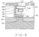
- FIG. 5illustrates a cross-sectional view of FIG. 4 along line A-A;
- FIG. 6illustrates a partially cutaway alternate layout of an inverter integrated circuit formed using the two-layer semiconductor of the present invention.
- FIG. 7illustrates a cross-sectional view of FIG. 6 along line B-B;
- FIG. 1shows a cross-section of a portion of an integrated circuit 100 having two overlapping semiconductor layers.
- the circuitis formed on a silicon substrate 102 and can be processed using steps similar to conventional flow-through source-drain formation.
- N-type transistors 103having gates 103 A, drains 103 B, and sources 106 are created in the P-type silicon substrate. N-wells are usually unnecessary.
- a salicide-block mask 106is used over the N-type junctions where a seed 108 for a second semiconductor layer of germanium is later to be formed.
- a first dielectric layer 109is deposited over the silicon substrate 102 and transistors 103 and it is planarized, then germanium islands 110 are formed by epitaxy lateral overgrowth (ELO) from seeds 108 using the substrate as a template.
- the ELO techniqueis used to form a high quality germanium seed 108 embedded in the insulator 109 formed on top of the silicon substrate 102 .
- insulator 109is formed as an oxide layer overlying a single crystal silicon substrate 102 . Seed windows are lithographically defined in the oxide and opened by etching down to the substrate. The exposed silicon surface is cleaned for germanium growth. Then, germanium is grown selectively on the exposed silicon by selective CVD growth.
- the growthis continued until the germanium overgrows the seed window and fills the region of the island 110 .
- the seeds and islandsare shaped and dimensioned so that defects originating at the Ge/Si interface are terminated at the seed walls before reaching the germanium island.
- Thisprovides a region of germanium 110 over the oxide mask that is essentially defect-free and is sufficiently large to form a germanium MOS transistor. Further details concerning this technique are set forth in U.S. Patent Application Publication No. 2004/0121507 A1 to Bude et al., herein incorporated by reference.
- the seeds 108 of the germanium islands 110are advantageously arranged to fall over N-type doping so that each island has a body tie. However, this is not an essential feature, as the body tie may also be created with an N-type implant and a contact from above.
- the seed 108 lying over N-type dopingpermits a closer overlap of N-type germanium islands 110 with transistors 103 in the substrate 102 .
- germanium P-type transistors 112having gates 112 A, drains 112 B, and sources 112 C are created in the germanium island 110 using steps familiar to those skilled in the art. Germanium processing temperatures are lower than silicon processing temperatures, hence, by forming the germanium layer after the silicon transistors have been created, the characteristics of both transistor types can be independently optimized without affecting one another.
- a second dielectric layer 114is deposited.
- Via holesare etched through the dielectric layers 114 , 109 to the silicon layer 102 and to the germanium layer 110 , and metal contacts 116 from a metal connector 118 to both types of transistors 103 , 112 are formed, using methods familiar to those skilled in the art of MOS processing.
- the P-type transistors 112can be as fast as the N-type transistor 103 , and their sizes may be equal. In contrast, in a conventional silicon-only layout, the P-type transistors must be twice as large as the N-type transistors to compensate for holes in silicon being slower than electrons.
- FIG. 2illustrates a conventionally formed inverter integrated circuit
- FIG. 3illustrates a conventionally formed NAND gate integrated circuit.
- a N-type tub 200 containing one or more PMOS transistor devices 202is located near a P-type tub 204 containing a matching number of NMOS transistor devices 206 .
- the N-type tub 200has a width 2 W which is typically about twice the width W of the P-type tub 204 to allow the drive of the PMOS transistors 202 to match the drive of the NMOS transistors 206 . Space must be allowed to provide for proper isolation between the P-type tub 204 and the N-type tub 200 , to avoid leakage and latchup.
- the NMOS transistor 206comprises a single N-polysilicon gate 208 , coupled via an inter-layer contact (ILC) to the input line 209 , which separates the N-drain 210 linked to the metal output line 211 from the N-source 212 linked to the metal ground 213 .
- ILCinter-layer contact
- a single P-polysilicon gate 214is coupled to the input line 209 , and separates the P-drain 216 , linked to the metal output line 211 , from the P-source 218 linked to the metal power line 220 .
- N-polysilicon gates 208divide the P-type tub 204 into two series connected NMOS transistors 206
- P-polysilicon gates 214divide the N-type tub 200 into two parallel connected PMOS transistors 202 , providing the correct logic function of a NAND gate having two inputs 209 A and 209 B.
- Other conventional gates and integrated electronic circuitsare laid out in similar fashion.
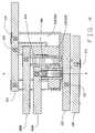
- FIG. 4shows a layout of a NAND gate formed using the two semiconductor layering method of the present invention.
- the N-type tub 204is advantageously placed directly over the P-type tub 200 and the PMOS gate 214 over the NMOS gate 208 .
- the P-type tub 200is s-shaped in this layout and the N-type tub 204 is shaped like a tuning fork.
- the P-type tub 200 and the N-type tub 204are divided by the polysilicon gate 208 and poly-germanium gate 214 , respectively, similar to the planar layout.
- a cross-section through the structure of FIG. 4 , taken along line A-Ais shown in FIG. 5 .
- the P-type transistor 202is above the N-type transistor 206 , and the gates 208 , 214 are stacked, with the surrounding space filled with the dielectric material 109 .
- FIG. 6an alternative layout is shown. This layout takes into account constraints on a particular growth technique.
- an opening (seed) 108 to the substrate 102should be opened in order to provide a template for the germanium island 110 .
- the germanium island 110is most easily formed if it is square and if the substrate opening (seed) 108 is near the center of the square.
- the seed opening 108therefore is not above the polysilicon or trench isolation 222 , and is advantageously over the exposed substrate 102 .
- FIG. 7illustrates a cross-section of the layout shown in FIG. 6 , taken along the line B-B.
- the two layouts utilizing a double semiconductor layering of the present inventionare much more compact than the corresponding conventional layering layouts where all the transistors are in a single plane. No extra spacing to separate the P-type tub 204 and the N-type tub 200 is required.
- the PMOS devices 202do not need to be any wider than the NMOS devices 206 because they are created in the germanium layer which has a higher mobility than the silicon substrate for both carriers.
- a silicon substratea silicon-on-insulator (SOI) substrate, a silicon-carbide substrate, or other silicon-based substrates may be used without departing from the scope of the present invention.
- SOIsilicon-on-insulator
- silicon-carbide substratesilicon-based substrates
- the described formation of the germanium layeris by epitaxial lateral overgrowth, other epitaxial layer formation techniques, for instance liquid-phase epitaxy (LPE) or wafer bonding may be used.
- LPEliquid-phase epitaxy
- other alloys of silicon-germanium and other semiconductorsmay be used, provided that (a) their chemistry is compatible with silicon; (b) they may be epitaxially grown from a silicon seed; and (c) their processing temperatures allow transistors to be created without destroying the silicon transistors in the substrate.
- the semiconductor material of the first layeris silicon
- the second layeris silicon-germanium
- the third layeris germanium. Alteration of the semiconductor layer conductivity types (NPN or PNP). would provide the desired isolation.
- a method of the present inventionprovides for the formation of an integrated circuit using at least two different semiconductor layers which are separated by dielectric layers.
- An upper layeris formed of a semiconductor which can be processed at a lower temperature than the lower layer.
- Transistors on the lower layerare created before the upper layer is grown, by epitaxy, using the substrate as a template. Transistors are then created in the upper layer.
- the two layersare interconnected using conventional wiring techniques.
- one layer of transistorsis of one carrier polarity, N-type or P-type, while each adjacent layer is of the opposite carrier polarity.
Landscapes
- Metal-Oxide And Bipolar Metal-Oxide Semiconductor Integrated Circuits (AREA)
- Bipolar Integrated Circuits (AREA)
Abstract
Description
Claims (18)
Priority Applications (3)
| Application Number | Priority Date | Filing Date | Title |
|---|---|---|---|
| US11/220,942US7589380B2 (en) | 2002-12-18 | 2005-09-07 | Method for forming integrated circuit utilizing dual semiconductors |
| PCT/US2006/032272WO2007030294A2 (en) | 2005-09-07 | 2006-08-18 | Method for forming integrated circuit utilizing dual semiconductors |
| TW095133098ATW200717773A (en) | 2005-09-07 | 2006-09-07 | Method for forming integrated circuit utilizing dual semiconductors |
Applications Claiming Priority (4)
| Application Number | Priority Date | Filing Date | Title |
|---|---|---|---|
| US43435902P | 2002-12-18 | 2002-12-18 | |
| US10/453,037US7012314B2 (en) | 2002-12-18 | 2003-06-03 | Semiconductor devices with reduced active region defects and unique contacting schemes |
| US60790104P | 2004-09-07 | 2004-09-07 | |
| US11/220,942US7589380B2 (en) | 2002-12-18 | 2005-09-07 | Method for forming integrated circuit utilizing dual semiconductors |
Related Parent Applications (1)
| Application Number | Title | Priority Date | Filing Date |
|---|---|---|---|
| US10/453,037Continuation-In-PartUS7012314B2 (en) | 2002-12-18 | 2003-06-03 | Semiconductor devices with reduced active region defects and unique contacting schemes |
Publications (2)
| Publication Number | Publication Date |
|---|---|
| US20060049409A1 US20060049409A1 (en) | 2006-03-09 |
| US7589380B2true US7589380B2 (en) | 2009-09-15 |
Family
ID=37836334
Family Applications (1)
| Application Number | Title | Priority Date | Filing Date |
|---|---|---|---|
| US11/220,942Active2026-08-20US7589380B2 (en) | 2002-12-18 | 2005-09-07 | Method for forming integrated circuit utilizing dual semiconductors |
Country Status (3)
| Country | Link |
|---|---|
| US (1) | US7589380B2 (en) |
| TW (1) | TW200717773A (en) |
| WO (1) | WO2007030294A2 (en) |
Cited By (2)
| Publication number | Priority date | Publication date | Assignee | Title |
|---|---|---|---|---|
| US8664739B2 (en) | 2002-12-18 | 2014-03-04 | Infrared Newco, Inc. | Image sensor comprising isolated germanium photodetectors integrated with a silicon substrate and silicon circuitry |
| US11901356B2 (en) | 2019-07-19 | 2024-02-13 | Samsung Electronics Co., Ltd. | Three-dimensional semiconductor devices |
Families Citing this family (33)
| Publication number | Priority date | Publication date | Assignee | Title |
|---|---|---|---|---|
| US9153645B2 (en)* | 2005-05-17 | 2015-10-06 | Taiwan Semiconductor Manufacturing Company, Ltd. | Lattice-mismatched semiconductor structures with reduced dislocation defect densities and related methods for device fabrication |
| EP2595175B1 (en)* | 2005-05-17 | 2019-04-17 | Taiwan Semiconductor Manufacturing Company, Ltd. | Method of fabricating a lattice-mismatched semiconductor structure with reduced dislocation defect densities |
| US20070267722A1 (en)* | 2006-05-17 | 2007-11-22 | Amberwave Systems Corporation | Lattice-mismatched semiconductor structures with reduced dislocation defect densities and related methods for device fabrication |
| US8324660B2 (en) | 2005-05-17 | 2012-12-04 | Taiwan Semiconductor Manufacturing Company, Ltd. | Lattice-mismatched semiconductor structures with reduced dislocation defect densities and related methods for device fabrication |
| KR101329388B1 (en)* | 2005-07-26 | 2013-11-14 | 앰버웨이브 시스템즈 코포레이션 | Solutions for integrated circuit integration of alternative active area materials |
| US20070054467A1 (en)* | 2005-09-07 | 2007-03-08 | Amberwave Systems Corporation | Methods for integrating lattice-mismatched semiconductor structure on insulators |
| US7638842B2 (en)* | 2005-09-07 | 2009-12-29 | Amberwave Systems Corporation | Lattice-mismatched semiconductor structures on insulators |
| KR101316947B1 (en)* | 2005-11-01 | 2013-10-15 | 메사추세츠 인스티튜트 오브 테크놀로지 | Monolithically integrated semiconductor materials and devices |
| WO2007067589A2 (en)* | 2005-12-05 | 2007-06-14 | Massachusetts Institute Of Technology | Insulated gate devices and method of making same |
| US7700461B2 (en)* | 2006-03-17 | 2010-04-20 | Samsung Electronics Co., Ltd. | Methods of laterally forming single crystalline thin film regions from seed layers |
| WO2007112066A2 (en) | 2006-03-24 | 2007-10-04 | Amberwave Systems Corporation | Lattice-mismatched semiconductor structures and related methods for device fabrication |
| US8063397B2 (en)* | 2006-06-28 | 2011-11-22 | Massachusetts Institute Of Technology | Semiconductor light-emitting structure and graded-composition substrate providing yellow-green light emission |
| US8173551B2 (en) | 2006-09-07 | 2012-05-08 | Taiwan Semiconductor Manufacturing Co., Ltd. | Defect reduction using aspect ratio trapping |
| US20080070355A1 (en)* | 2006-09-18 | 2008-03-20 | Amberwave Systems Corporation | Aspect ratio trapping for mixed signal applications |
| WO2008039495A1 (en) | 2006-09-27 | 2008-04-03 | Amberwave Systems Corporation | Tri-gate field-effect transistors formed by aspect ratio trapping |
| WO2008039534A2 (en) | 2006-09-27 | 2008-04-03 | Amberwave Systems Corporation | Quantum tunneling devices and circuits with lattice- mismatched semiconductor structures |
| US8502263B2 (en)* | 2006-10-19 | 2013-08-06 | Taiwan Semiconductor Manufacturing Company, Ltd. | Light-emitter-based devices with lattice-mismatched semiconductor structures |
| US8304805B2 (en)* | 2009-01-09 | 2012-11-06 | Taiwan Semiconductor Manufacturing Company, Ltd. | Semiconductor diodes fabricated by aspect ratio trapping with coalesced films |
| US8237151B2 (en) | 2009-01-09 | 2012-08-07 | Taiwan Semiconductor Manufacturing Company, Ltd. | Diode-based devices and methods for making the same |
| US7825328B2 (en) | 2007-04-09 | 2010-11-02 | Taiwan Semiconductor Manufacturing Company, Ltd. | Nitride-based multi-junction solar cell modules and methods for making the same |
| WO2008124154A2 (en) | 2007-04-09 | 2008-10-16 | Amberwave Systems Corporation | Photovoltaics on silicon |
| US8329541B2 (en) | 2007-06-15 | 2012-12-11 | Taiwan Semiconductor Manufacturing Company, Ltd. | InP-based transistor fabrication |
| JP2010538495A (en) | 2007-09-07 | 2010-12-09 | アンバーウェーブ・システムズ・コーポレーション | Multi-junction solar cell |
| US8183667B2 (en) | 2008-06-03 | 2012-05-22 | Taiwan Semiconductor Manufacturing Co., Ltd. | Epitaxial growth of crystalline material |
| US8274097B2 (en) | 2008-07-01 | 2012-09-25 | Taiwan Semiconductor Manufacturing Company, Ltd. | Reduction of edge effects from aspect ratio trapping |
| US8981427B2 (en) | 2008-07-15 | 2015-03-17 | Taiwan Semiconductor Manufacturing Company, Ltd. | Polishing of small composite semiconductor materials |
| EP2335273A4 (en) | 2008-09-19 | 2012-01-25 | Taiwan Semiconductor Mfg | FORMATION OF DEVICES BY GROWTH OF EPITAXIAL LAYERS |
| US20100072515A1 (en)* | 2008-09-19 | 2010-03-25 | Amberwave Systems Corporation | Fabrication and structures of crystalline material |
| US8253211B2 (en)* | 2008-09-24 | 2012-08-28 | Taiwan Semiconductor Manufacturing Company, Ltd. | Semiconductor sensor structures with reduced dislocation defect densities |
| US8629446B2 (en) | 2009-04-02 | 2014-01-14 | Taiwan Semiconductor Manufacturing Company, Ltd. | Devices formed from a non-polar plane of a crystalline material and method of making the same |
| TWI566328B (en)* | 2013-07-29 | 2017-01-11 | 高效電源轉換公司 | Gallium nitride transistor having a polysilicon layer for generating additional components |
| WO2018063160A1 (en)* | 2016-09-27 | 2018-04-05 | Intel Corporation | METHODS AND APPARATUS TO FORM GaN-BASED TRANSISTORS DURING BACK-END-OF-LINE PROCESSING |
| TW201840903A (en)* | 2016-11-20 | 2018-11-16 | 美商應用材料股份有限公司 | Methods to selectively deposit corrosion-free metal contacts |
Citations (21)
| Publication number | Priority date | Publication date | Assignee | Title |
|---|---|---|---|---|
| US4038680A (en) | 1972-12-29 | 1977-07-26 | Sony Corporation | Semiconductor integrated circuit device |
| JPS6191917A (en) | 1984-10-12 | 1986-05-10 | Nippon Telegr & Teleph Corp <Ntt> | Manufacture of semiconductor thin film crystal |
| US4952526A (en) | 1988-04-05 | 1990-08-28 | Thomson-Csf | Method for the fabrication of an alternation of layers of monocrystalline semiconducting material and layers of insulating material |
| US5120666A (en) | 1989-05-16 | 1992-06-09 | Fujitsu Limited | Manufacturing method for semiconductor device |
| US5467204A (en) | 1991-12-09 | 1995-11-14 | Sharp Kabushiki Kaisha | Liquid crystal light valve with dual function as both optical-to-electrical and optical-to-optical transducer |
| US5770483A (en)* | 1996-10-08 | 1998-06-23 | Advanced Micro Devices, Inc. | Multi-level transistor fabrication method with high performance drain-to-gate connection |
| US5838047A (en)* | 1995-06-16 | 1998-11-17 | Mitsubishi Denki Kabushiki Kaisha | CMOS substrate biasing for threshold voltage control |
| JP2001223224A (en) | 2000-01-10 | 2001-08-17 | Internatl Business Mach Corp <Ibm> | Method for forming silicon-germanium base in heterojunction bipolar transistor |
| US6287903B1 (en) | 1997-12-24 | 2001-09-11 | Texas Instruments Incorporated | Structure and method for a large-permittivity dielectric using a germanium layer |
| US6455360B1 (en) | 1995-06-26 | 2002-09-24 | Seiko Epson Corporation | Method for forming crystalline semiconductor layers, a method for fabricating thin film transistors, and a method for fabricating solar cells and active matrix liquid crystal devices |
| US20030027409A1 (en) | 2001-08-02 | 2003-02-06 | Motorola, Inc. | Germanium semiconductor structure, integrated circuit, and process for fabricating the same |
| US20030057439A1 (en) | 2001-08-09 | 2003-03-27 | Fitzgerald Eugene A. | Dual layer CMOS devices |
| US20030207127A1 (en) | 2002-02-21 | 2003-11-06 | Anand Murthy | Method of forming a germanium film on a semiconductor substrate that includes the formation of a graded silicon-germanium buffer layer prior to the formation of a germanium layer |
| US20040026765A1 (en) | 2002-06-07 | 2004-02-12 | Amberwave Systems Corporation | Semiconductor devices having strained dual channel layers |
| US20040029325A1 (en) | 2000-06-23 | 2004-02-12 | Le Goascoz Vincent | Method for making a soi semiconductor substrate with thin active semiconductor layer |
| US20040106268A1 (en) | 2002-05-07 | 2004-06-03 | Shaheen Mohamad A. | Thermally stable crystalline defect-free germanium boned to silicon and silicon dioxide |
| US20040222463A1 (en) | 2003-05-09 | 2004-11-11 | Yee-Chia Yeo | SOI chip with mesa isolation and recess resistant regions |
| US20050093028A1 (en) | 2003-10-29 | 2005-05-05 | Chambers James J. | Multiple-gate MOSFET device with lithography independent silicon body thickness and methods for fabricating the same |
| US20050099839A1 (en)* | 2003-03-11 | 2005-05-12 | Arup Bhattacharyya | Methods for machine detection of al least one aspect of an object, methods for machine identification of a person, and methods of forming electronic systems |
| US6900499B2 (en) | 1997-08-29 | 2005-05-31 | Semiconductor Energy Laboratory Co., Ltd. | Non-volatile memory and semiconductor device |
| US7012314B2 (en) | 2002-12-18 | 2006-03-14 | Agere Systems Inc. | Semiconductor devices with reduced active region defects and unique contacting schemes |
- 2005
- 2005-09-07USUS11/220,942patent/US7589380B2/enactiveActive
- 2006
- 2006-08-18WOPCT/US2006/032272patent/WO2007030294A2/enactiveApplication Filing
- 2006-09-07TWTW095133098Apatent/TW200717773A/enunknown
Patent Citations (21)
| Publication number | Priority date | Publication date | Assignee | Title |
|---|---|---|---|---|
| US4038680A (en) | 1972-12-29 | 1977-07-26 | Sony Corporation | Semiconductor integrated circuit device |
| JPS6191917A (en) | 1984-10-12 | 1986-05-10 | Nippon Telegr & Teleph Corp <Ntt> | Manufacture of semiconductor thin film crystal |
| US4952526A (en) | 1988-04-05 | 1990-08-28 | Thomson-Csf | Method for the fabrication of an alternation of layers of monocrystalline semiconducting material and layers of insulating material |
| US5120666A (en) | 1989-05-16 | 1992-06-09 | Fujitsu Limited | Manufacturing method for semiconductor device |
| US5467204A (en) | 1991-12-09 | 1995-11-14 | Sharp Kabushiki Kaisha | Liquid crystal light valve with dual function as both optical-to-electrical and optical-to-optical transducer |
| US5838047A (en)* | 1995-06-16 | 1998-11-17 | Mitsubishi Denki Kabushiki Kaisha | CMOS substrate biasing for threshold voltage control |
| US6455360B1 (en) | 1995-06-26 | 2002-09-24 | Seiko Epson Corporation | Method for forming crystalline semiconductor layers, a method for fabricating thin film transistors, and a method for fabricating solar cells and active matrix liquid crystal devices |
| US5770483A (en)* | 1996-10-08 | 1998-06-23 | Advanced Micro Devices, Inc. | Multi-level transistor fabrication method with high performance drain-to-gate connection |
| US6900499B2 (en) | 1997-08-29 | 2005-05-31 | Semiconductor Energy Laboratory Co., Ltd. | Non-volatile memory and semiconductor device |
| US6287903B1 (en) | 1997-12-24 | 2001-09-11 | Texas Instruments Incorporated | Structure and method for a large-permittivity dielectric using a germanium layer |
| JP2001223224A (en) | 2000-01-10 | 2001-08-17 | Internatl Business Mach Corp <Ibm> | Method for forming silicon-germanium base in heterojunction bipolar transistor |
| US20040029325A1 (en) | 2000-06-23 | 2004-02-12 | Le Goascoz Vincent | Method for making a soi semiconductor substrate with thin active semiconductor layer |
| US20030027409A1 (en) | 2001-08-02 | 2003-02-06 | Motorola, Inc. | Germanium semiconductor structure, integrated circuit, and process for fabricating the same |
| US20030057439A1 (en) | 2001-08-09 | 2003-03-27 | Fitzgerald Eugene A. | Dual layer CMOS devices |
| US20030207127A1 (en) | 2002-02-21 | 2003-11-06 | Anand Murthy | Method of forming a germanium film on a semiconductor substrate that includes the formation of a graded silicon-germanium buffer layer prior to the formation of a germanium layer |
| US20040106268A1 (en) | 2002-05-07 | 2004-06-03 | Shaheen Mohamad A. | Thermally stable crystalline defect-free germanium boned to silicon and silicon dioxide |
| US20040026765A1 (en) | 2002-06-07 | 2004-02-12 | Amberwave Systems Corporation | Semiconductor devices having strained dual channel layers |
| US7012314B2 (en) | 2002-12-18 | 2006-03-14 | Agere Systems Inc. | Semiconductor devices with reduced active region defects and unique contacting schemes |
| US20050099839A1 (en)* | 2003-03-11 | 2005-05-12 | Arup Bhattacharyya | Methods for machine detection of al least one aspect of an object, methods for machine identification of a person, and methods of forming electronic systems |
| US20040222463A1 (en) | 2003-05-09 | 2004-11-11 | Yee-Chia Yeo | SOI chip with mesa isolation and recess resistant regions |
| US20050093028A1 (en) | 2003-10-29 | 2005-05-05 | Chambers James J. | Multiple-gate MOSFET device with lithography independent silicon body thickness and methods for fabricating the same |
Non-Patent Citations (2)
| Title |
|---|
| International Search Report mailed Feb. 12, 2008 from the International Searching Authority for International Application No. PCT/US 06/32272. |
| Written Opinion mailed Feb. 12, 2008 from the International Searching Authority for International Application No. PCT/US 06/32272. |
Cited By (3)
| Publication number | Priority date | Publication date | Assignee | Title |
|---|---|---|---|---|
| US8664739B2 (en) | 2002-12-18 | 2014-03-04 | Infrared Newco, Inc. | Image sensor comprising isolated germanium photodetectors integrated with a silicon substrate and silicon circuitry |
| US9142585B2 (en) | 2002-12-18 | 2015-09-22 | Infrared Newco, Inc. | Image sensor comprising isolated germanium photodetectors integrated with a silicon substrate and silicon circuitry |
| US11901356B2 (en) | 2019-07-19 | 2024-02-13 | Samsung Electronics Co., Ltd. | Three-dimensional semiconductor devices |
Also Published As
| Publication number | Publication date |
|---|---|
| US20060049409A1 (en) | 2006-03-09 |
| WO2007030294A2 (en) | 2007-03-15 |
| WO2007030294A3 (en) | 2009-04-30 |
| TW200717773A (en) | 2007-05-01 |
Similar Documents
| Publication | Publication Date | Title |
|---|---|---|
| US7589380B2 (en) | Method for forming integrated circuit utilizing dual semiconductors | |
| US7405436B2 (en) | Stressed field effect transistors on hybrid orientation substrate | |
| JP4814304B2 (en) | Integrated circuit and manufacturing method thereof | |
| US7619300B2 (en) | Super hybrid SOI CMOS devices | |
| US7989296B2 (en) | Semiconductor device and method of manufacturing same | |
| US7034362B2 (en) | Double silicon-on-insulator (SOI) metal oxide semiconductor field effect transistor (MOSFET) structures | |
| US7915100B2 (en) | Hybrid orientation CMOS with partial insulation process | |
| CN100479161C (en) | Semiconductor device and method of manufacturing same | |
| US6881621B2 (en) | Method of fabricating SOI substrate having an etch stop layer, and method of fabricating SOI integrated circuit using the same | |
| US6689648B2 (en) | Semiconductor device having silicon on insulator and fabricating method therefor | |
| US9607986B2 (en) | Mixed orientation semiconductor device and method | |
| WO2005112127A1 (en) | SEMICONDUCTOR DEVICE BASED ON Si-Ge WITH HIGH STRESS LINER FOR ENHANCED CHANNEL CARRIER MOBILITY | |
| CN100536144C (en) | Semiconductor device, substrate structure of semiconductor device and method for forming the same | |
| US7285831B2 (en) | CMOS device with improved performance and method of fabricating the same | |
| US8017472B2 (en) | CMOS devices having stress-altering material lining the isolation trenches and methods of manufacturing thereof | |
| US8053844B2 (en) | Hybrid orientation scheme for standard orthogonal circuits | |
| US6512275B1 (en) | Semiconductor integrated circuits | |
| US11545483B2 (en) | Nanosheet (NS) and fin field-effect transistor (FinFET) hybrid integration | |
| US10978572B2 (en) | Self-aligned contact with metal-insulator transition materials | |
| US7790522B2 (en) | Defect-free hybrid orientation technology for semiconductor devices | |
| US7986029B2 (en) | Dual SOI structure |
Legal Events
| Date | Code | Title | Description |
|---|---|---|---|
| AS | Assignment | Owner name:NOBLE DEVICE TECHNOLOGIES, CORP., NEW JERSEY Free format text:ASSIGNMENT OF ASSIGNORS INTEREST;ASSIGNORS:RAFFERTY, CONOR S.;KING, CLIFFORD ALAN;REEL/FRAME:017234/0667 Effective date:20051110 | |
| AS | Assignment | Owner name:NOBLE PEAK VISION CORP., MASSACHUSETTS Free format text:CHANGE OF NAME;ASSIGNOR:NOBLE DEVICE TECHNOLOGIES CORPORATION;REEL/FRAME:019874/0166 Effective date:20070309 | |
| STCF | Information on status: patent grant | Free format text:PATENTED CASE | |
| CC | Certificate of correction | ||
| AS | Assignment | Owner name:INFRARED NEWCO, INC., ARIZONA Free format text:ASSIGNMENT OF ASSIGNORS INTEREST;ASSIGNOR:NOBLEPEAK VISION CORP.;REEL/FRAME:025855/0453 Effective date:20101230 | |
| REMI | Maintenance fee reminder mailed | ||
| FPAY | Fee payment | Year of fee payment:4 | |
| SULP | Surcharge for late payment | ||
| FPAY | Fee payment | Year of fee payment:8 | |
| AS | Assignment | Owner name:SEMIKING LLC, MASSACHUSETTS Free format text:NOTICE OF EXCLUSIVE LICENSE AND PURCHASE OPTION;ASSIGNOR:INFRARED LABORATORIES, INC.;REEL/FRAME:049149/0252 Effective date:20190509 | |
| FEPP | Fee payment procedure | Free format text:MAINTENANCE FEE REMINDER MAILED (ORIGINAL EVENT CODE: REM.); ENTITY STATUS OF PATENT OWNER: SMALL ENTITY | |
| FEPP | Fee payment procedure | Free format text:11.5 YR SURCHARGE- LATE PMT W/IN 6 MO, SMALL ENTITY (ORIGINAL EVENT CODE: M2556); ENTITY STATUS OF PATENT OWNER: SMALL ENTITY | |
| MAFP | Maintenance fee payment | Free format text:PAYMENT OF MAINTENANCE FEE, 12TH YR, SMALL ENTITY (ORIGINAL EVENT CODE: M2553); ENTITY STATUS OF PATENT OWNER: SMALL ENTITY Year of fee payment:12 | |
| AS | Assignment | Owner name:TRUST B UNDER THE FRANK J. AND EDITH M. LOW TRUST, DATED APRIL 26, 2007, ARKANSAS Free format text:RELEASE BY SECURED PARTY;ASSIGNOR:INFRARED LABORATORIES INCORPORATED;REEL/FRAME:065645/0974 Effective date:20231109 Owner name:ARKTONICS, LLC, ARKANSAS Free format text:ASSIGNMENT OF ASSIGNORS INTEREST;ASSIGNOR:INFRARED LABORATORIES, INC.;REEL/FRAME:065645/0801 Effective date:20231120 |