US7588736B2 - Apparatus and method for generating a chemical precursor - Google Patents
Apparatus and method for generating a chemical precursorDownload PDFInfo
- Publication number
- US7588736B2 US7588736B2US11/383,642US38364206AUS7588736B2US 7588736 B2US7588736 B2US 7588736B2US 38364206 AUS38364206 AUS 38364206AUS 7588736 B2US7588736 B2US 7588736B2
- Authority
- US
- United States
- Prior art keywords
- canister
- interior volume
- precursor
- baffles
- tantalum
- Prior art date
- Legal status (The legal status is an assumption and is not a legal conclusion. Google has not performed a legal analysis and makes no representation as to the accuracy of the status listed.)
- Expired - Lifetime, expires
Links
- 239000012707chemical precursorSubstances0.000titleclaimsabstractdescription8
- 238000000034methodMethods0.000titledescription36
- 239000012530fluidSubstances0.000claimsabstract6
- 238000007740vapor depositionMethods0.000claimsabstract6
- 239000002243precursorSubstances0.000claimsdescription83
- 239000000463materialSubstances0.000claimsdescription69
- GUVRBAGPIYLISA-UHFFFAOYSA-Ntantalum atomChemical compound[Ta]GUVRBAGPIYLISA-UHFFFAOYSA-N0.000claimsdescription50
- 229910052715tantalumInorganic materials0.000claimsdescription49
- 239000007787solidSubstances0.000claimsdescription23
- 239000002245particleSubstances0.000claimsdescription21
- 239000000203mixtureSubstances0.000claimsdescription14
- 229910052751metalInorganic materials0.000claimsdescription8
- 239000002184metalSubstances0.000claimsdescription8
- 238000011049fillingMethods0.000claimsdescription6
- ZAMOUSCENKQFHK-UHFFFAOYSA-NChlorine atomChemical compound[Cl]ZAMOUSCENKQFHK-UHFFFAOYSA-N0.000claimsdescription5
- 229910052801chlorineInorganic materials0.000claimsdescription5
- 239000000460chlorineSubstances0.000claimsdescription5
- 239000012535impuritySubstances0.000claimsdescription5
- 229910052582BNInorganic materials0.000claimsdescription2
- PZNSFCLAULLKQX-UHFFFAOYSA-NBoron nitrideChemical compoundN#BPZNSFCLAULLKQX-UHFFFAOYSA-N0.000claimsdescription2
- PMHQVHHXPFUNSP-UHFFFAOYSA-Mcopper(1+);methylsulfanylmethane;bromideChemical compoundBr[Cu].CSCPMHQVHHXPFUNSP-UHFFFAOYSA-M0.000claimsdescription2
- 239000007789gasSubstances0.000description73
- 239000010410layerSubstances0.000description41
- 239000012159carrier gasSubstances0.000description28
- 150000001875compoundsChemical class0.000description26
- 239000007788liquidSubstances0.000description25
- 239000000758substrateSubstances0.000description24
- 230000004888barrier functionEffects0.000description18
- XKRFYHLGVUSROY-UHFFFAOYSA-NArgonChemical compound[Ar]XKRFYHLGVUSROY-UHFFFAOYSA-N0.000description16
- -1nitrogen containing compoundChemical class0.000description15
- 238000000151depositionMethods0.000description13
- 239000002356single layerSubstances0.000description13
- 239000002002slurrySubstances0.000description13
- RYGMFSIKBFXOCR-UHFFFAOYSA-NCopperChemical compound[Cu]RYGMFSIKBFXOCR-UHFFFAOYSA-N0.000description12
- 238000000231atomic layer depositionMethods0.000description12
- 229910052802copperInorganic materials0.000description12
- 239000010949copperSubstances0.000description12
- MZLGASXMSKOWSE-UHFFFAOYSA-Ntantalum nitrideChemical compound[Ta]#NMZLGASXMSKOWSE-UHFFFAOYSA-N0.000description12
- 239000003921oilSubstances0.000description11
- 229910052786argonInorganic materials0.000description8
- 238000010438heat treatmentMethods0.000description8
- QJGQUHMNIGDVPM-UHFFFAOYSA-Nnitrogen groupChemical group[N]QJGQUHMNIGDVPM-UHFFFAOYSA-N0.000description7
- 238000010926purgeMethods0.000description7
- NJIAKNWTIVDSDA-FQEVSTJZSA-N7-[4-(1-methylsulfonylpiperidin-4-yl)phenyl]-n-[[(2s)-morpholin-2-yl]methyl]pyrido[3,4-b]pyrazin-5-amineChemical compoundC1CN(S(=O)(=O)C)CCC1C1=CC=C(C=2N=C(NC[C@H]3OCCNC3)C3=NC=CN=C3C=2)C=C1NJIAKNWTIVDSDA-FQEVSTJZSA-N0.000description6
- IJGRMHOSHXDMSA-UHFFFAOYSA-NAtomic nitrogenChemical compoundN#NIJGRMHOSHXDMSA-UHFFFAOYSA-N0.000description6
- FQNHWXHRAUXLFU-UHFFFAOYSA-Ncarbon monoxide;tungstenChemical group[W].[O+]#[C-].[O+]#[C-].[O+]#[C-].[O+]#[C-].[O+]#[C-].[O+]#[C-]FQNHWXHRAUXLFU-UHFFFAOYSA-N0.000description6
- QGZKDVFQNNGYKY-UHFFFAOYSA-NAmmoniaChemical compoundNQGZKDVFQNNGYKY-UHFFFAOYSA-N0.000description5
- 230000015572biosynthetic processEffects0.000description5
- 230000008021depositionEffects0.000description5
- 238000005516engineering processMethods0.000description5
- 230000008016vaporizationEffects0.000description5
- OAKJQQAXSVQMHS-UHFFFAOYSA-NHydrazineChemical compoundNNOAKJQQAXSVQMHS-UHFFFAOYSA-N0.000description4
- 239000006227byproductSubstances0.000description4
- 238000006243chemical reactionMethods0.000description4
- 238000009792diffusion processMethods0.000description4
- 150000004820halidesChemical class0.000description4
- 239000000047productSubstances0.000description4
- 238000000859sublimationMethods0.000description4
- 230000008022sublimationEffects0.000description4
- 238000005979thermal decomposition reactionMethods0.000description4
- 238000009834vaporizationMethods0.000description4
- VYPSYNLAJGMNEJ-UHFFFAOYSA-NSilicium dioxideChemical compoundO=[Si]=OVYPSYNLAJGMNEJ-UHFFFAOYSA-N0.000description3
- PCFKSVCJYMINSV-UHFFFAOYSA-N[Ta+5].[N-]=O.[N-]=O.[N-]=O.[N-]=O.[N-]=OChemical class[Ta+5].[N-]=O.[N-]=O.[N-]=O.[N-]=O.[N-]=OPCFKSVCJYMINSV-UHFFFAOYSA-N0.000description3
- 239000001307heliumSubstances0.000description3
- 229910052734heliumInorganic materials0.000description3
- SWQJXJOGLNCZEY-UHFFFAOYSA-Nhelium atomChemical compound[He]SWQJXJOGLNCZEY-UHFFFAOYSA-N0.000description3
- 230000010354integrationEffects0.000description3
- 238000004519manufacturing processMethods0.000description3
- 238000002156mixingMethods0.000description3
- 239000006187pillSubstances0.000description3
- 239000004065semiconductorSubstances0.000description3
- XEEYBQQBJWHFJM-UHFFFAOYSA-NIronChemical compound[Fe]XEEYBQQBJWHFJM-UHFFFAOYSA-N0.000description2
- XUIMIQQOPSSXEZ-UHFFFAOYSA-NSiliconChemical compound[Si]XUIMIQQOPSSXEZ-UHFFFAOYSA-N0.000description2
- 238000013019agitationMethods0.000description2
- 229910052782aluminiumInorganic materials0.000description2
- XAGFODPZIPBFFR-UHFFFAOYSA-NaluminiumChemical compound[Al]XAGFODPZIPBFFR-UHFFFAOYSA-N0.000description2
- 239000004020conductorSubstances0.000description2
- 238000011109contaminationMethods0.000description2
- 239000003989dielectric materialSubstances0.000description2
- 230000000694effectsEffects0.000description2
- 239000001257hydrogenSubstances0.000description2
- 229910052739hydrogenInorganic materials0.000description2
- 125000004435hydrogen atomChemical class[H]*0.000description2
- 230000013011matingEffects0.000description2
- 229910052757nitrogenInorganic materials0.000description2
- 229910000069nitrogen hydrideInorganic materials0.000description2
- 239000000376reactantSubstances0.000description2
- 230000001105regulatory effectEffects0.000description2
- 229910052710siliconInorganic materials0.000description2
- 239000010703siliconSubstances0.000description2
- 239000000126substanceSubstances0.000description2
- MNWRORMXBIWXCI-UHFFFAOYSA-Ntetrakis(dimethylamido)titaniumChemical compoundCN(C)[Ti](N(C)C)(N(C)C)N(C)CMNWRORMXBIWXCI-UHFFFAOYSA-N0.000description2
- MAUMSNABMVEOGP-UHFFFAOYSA-N(methyl-$l^{2}-azanyl)methaneChemical compoundC[N]CMAUMSNABMVEOGP-UHFFFAOYSA-N0.000description1
- DIIIISSCIXVANO-UHFFFAOYSA-N1,2-DimethylhydrazineChemical compoundCNNCDIIIISSCIXVANO-UHFFFAOYSA-N0.000description1
- BLIQUJLAJXRXSG-UHFFFAOYSA-N1-benzyl-3-(trifluoromethyl)pyrrolidin-1-ium-3-carboxylateChemical compoundC1C(C(=O)O)(C(F)(F)F)CCN1CC1=CC=CC=C1BLIQUJLAJXRXSG-UHFFFAOYSA-N0.000description1
- ZCYVEMRRCGMTRW-UHFFFAOYSA-N7553-56-2Chemical compound[I]ZCYVEMRRCGMTRW-UHFFFAOYSA-N0.000description1
- WKBOTKDWSSQWDR-UHFFFAOYSA-NBromine atomChemical compound[Br]WKBOTKDWSSQWDR-UHFFFAOYSA-N0.000description1
- PXGOKWXKJXAPGV-UHFFFAOYSA-NFluorineChemical compoundFFPXGOKWXKJXAPGV-UHFFFAOYSA-N0.000description1
- WHXSMMKQMYFTQS-UHFFFAOYSA-NLithiumChemical compound[Li]WHXSMMKQMYFTQS-UHFFFAOYSA-N0.000description1
- 239000007983Tris bufferSubstances0.000description1
- 239000000853adhesiveSubstances0.000description1
- 230000001070adhesive effectEffects0.000description1
- 239000000956alloySubstances0.000description1
- 229910045601alloyInorganic materials0.000description1
- WYTGDNHDOZPMIW-RCBQFDQVSA-NalstonineNatural productsC1=CC2=C3C=CC=CC3=NC2=C2N1C[C@H]1[C@H](C)OC=C(C(=O)OC)[C@H]1C2WYTGDNHDOZPMIW-RCBQFDQVSA-N0.000description1
- 229910021529ammoniaInorganic materials0.000description1
- 239000003708ampulSubstances0.000description1
- 239000011324beadSubstances0.000description1
- 230000009286beneficial effectEffects0.000description1
- 230000033228biological regulationEffects0.000description1
- WYEMLYFITZORAB-UHFFFAOYSA-NboscalidChemical compoundC1=CC(Cl)=CC=C1C1=CC=CC=C1NC(=O)C1=CC=CN=C1ClWYEMLYFITZORAB-UHFFFAOYSA-N0.000description1
- GDTBXPJZTBHREO-UHFFFAOYSA-NbromineSubstancesBrBrGDTBXPJZTBHREO-UHFFFAOYSA-N0.000description1
- 229910052794bromiumInorganic materials0.000description1
- 238000005229chemical vapour depositionMethods0.000description1
- 239000011248coating agentSubstances0.000description1
- 238000000576coating methodMethods0.000description1
- 238000010276constructionMethods0.000description1
- 239000000356contaminantSubstances0.000description1
- 238000001816coolingMethods0.000description1
- 230000008878couplingEffects0.000description1
- 238000010168coupling processMethods0.000description1
- 238000005859coupling reactionMethods0.000description1
- 238000000354decomposition reactionMethods0.000description1
- 230000007547defectEffects0.000description1
- 238000005137deposition processMethods0.000description1
- 125000002147dimethylamino groupChemical group[H]C([H])([H])N(*)C([H])([H])[H]0.000description1
- VSLPMIMVDUOYFW-UHFFFAOYSA-Ndimethylazanide;tantalum(5+)Chemical compound[Ta+5].C[N-]C.C[N-]C.C[N-]C.C[N-]C.C[N-]CVSLPMIMVDUOYFW-UHFFFAOYSA-N0.000description1
- 238000009826distributionMethods0.000description1
- 230000009977dual effectEffects0.000description1
- 238000009713electroplatingMethods0.000description1
- UCSVJZQSZZAKLD-UHFFFAOYSA-Nethyl azideChemical compoundCCN=[N+]=[N-]UCSVJZQSZZAKLD-UHFFFAOYSA-N0.000description1
- 229910052731fluorineInorganic materials0.000description1
- 239000011737fluorineSubstances0.000description1
- ZHPNWZCWUUJAJC-UHFFFAOYSA-NfluorosiliconChemical compound[Si]FZHPNWZCWUUJAJC-UHFFFAOYSA-N0.000description1
- 229910052736halogenInorganic materials0.000description1
- 150000002367halogensChemical class0.000description1
- 150000002429hydrazinesChemical class0.000description1
- 239000011261inert gasSubstances0.000description1
- 229910052740iodineInorganic materials0.000description1
- 239000011630iodineSubstances0.000description1
- 229910052742ironInorganic materials0.000description1
- 239000012705liquid precursorSubstances0.000description1
- 229910052744lithiumInorganic materials0.000description1
- 238000001465metallisationMethods0.000description1
- 150000002739metalsChemical class0.000description1
- WDCKRYQAVLUEDJ-UHFFFAOYSA-Nmethyl(oxo)siliconChemical compoundC[Si]=OWDCKRYQAVLUEDJ-UHFFFAOYSA-N0.000description1
- 229910052759nickelInorganic materials0.000description1
- PXHVJJICTQNCMI-UHFFFAOYSA-NnickelSubstances[Ni]PXHVJJICTQNCMI-UHFFFAOYSA-N0.000description1
- 125000004433nitrogen atomChemical groupN*0.000description1
- 125000002524organometallic groupChemical group0.000description1
- HKOOXMFOFWEVGF-UHFFFAOYSA-NphenylhydrazineChemical compoundNNC1=CC=CC=C1HKOOXMFOFWEVGF-UHFFFAOYSA-N0.000description1
- 229940067157phenylhydrazineDrugs0.000description1
- 238000005240physical vapour depositionMethods0.000description1
- 238000005498polishingMethods0.000description1
- 238000007789sealingMethods0.000description1
- 235000012239silicon dioxideNutrition0.000description1
- 239000000377silicon dioxideSubstances0.000description1
- 229910052814silicon oxideInorganic materials0.000description1
- 238000005092sublimation methodMethods0.000description1
- 239000000725suspensionSubstances0.000description1
- MUQNAPSBHXFMHT-UHFFFAOYSA-Ntert-butylhydrazineChemical compoundCC(C)(C)NNMUQNAPSBHXFMHT-UHFFFAOYSA-N0.000description1
- 238000011144upstream manufacturingMethods0.000description1
- 238000005019vapor deposition processMethods0.000description1
- XLYOFNOQVPJJNP-UHFFFAOYSA-NwaterChemical compoundOXLYOFNOQVPJJNP-UHFFFAOYSA-N0.000description1
- 238000003466weldingMethods0.000description1
Images


Classifications
- C—CHEMISTRY; METALLURGY
- C23—COATING METALLIC MATERIAL; COATING MATERIAL WITH METALLIC MATERIAL; CHEMICAL SURFACE TREATMENT; DIFFUSION TREATMENT OF METALLIC MATERIAL; COATING BY VACUUM EVAPORATION, BY SPUTTERING, BY ION IMPLANTATION OR BY CHEMICAL VAPOUR DEPOSITION, IN GENERAL; INHIBITING CORROSION OF METALLIC MATERIAL OR INCRUSTATION IN GENERAL
- C23C—COATING METALLIC MATERIAL; COATING MATERIAL WITH METALLIC MATERIAL; SURFACE TREATMENT OF METALLIC MATERIAL BY DIFFUSION INTO THE SURFACE, BY CHEMICAL CONVERSION OR SUBSTITUTION; COATING BY VACUUM EVAPORATION, BY SPUTTERING, BY ION IMPLANTATION OR BY CHEMICAL VAPOUR DEPOSITION, IN GENERAL
- C23C16/00—Chemical coating by decomposition of gaseous compounds, without leaving reaction products of surface material in the coating, i.e. chemical vapour deposition [CVD] processes
- C23C16/44—Chemical coating by decomposition of gaseous compounds, without leaving reaction products of surface material in the coating, i.e. chemical vapour deposition [CVD] processes characterised by the method of coating
- C23C16/455—Chemical coating by decomposition of gaseous compounds, without leaving reaction products of surface material in the coating, i.e. chemical vapour deposition [CVD] processes characterised by the method of coating characterised by the method used for introducing gases into reaction chamber or for modifying gas flows in reaction chamber
- C23C16/45523—Pulsed gas flow or change of composition over time
- C23C16/45525—Atomic layer deposition [ALD]
- C23C16/45544—Atomic layer deposition [ALD] characterized by the apparatus
- C—CHEMISTRY; METALLURGY
- C23—COATING METALLIC MATERIAL; COATING MATERIAL WITH METALLIC MATERIAL; CHEMICAL SURFACE TREATMENT; DIFFUSION TREATMENT OF METALLIC MATERIAL; COATING BY VACUUM EVAPORATION, BY SPUTTERING, BY ION IMPLANTATION OR BY CHEMICAL VAPOUR DEPOSITION, IN GENERAL; INHIBITING CORROSION OF METALLIC MATERIAL OR INCRUSTATION IN GENERAL
- C23C—COATING METALLIC MATERIAL; COATING MATERIAL WITH METALLIC MATERIAL; SURFACE TREATMENT OF METALLIC MATERIAL BY DIFFUSION INTO THE SURFACE, BY CHEMICAL CONVERSION OR SUBSTITUTION; COATING BY VACUUM EVAPORATION, BY SPUTTERING, BY ION IMPLANTATION OR BY CHEMICAL VAPOUR DEPOSITION, IN GENERAL
- C23C16/00—Chemical coating by decomposition of gaseous compounds, without leaving reaction products of surface material in the coating, i.e. chemical vapour deposition [CVD] processes
- C23C16/44—Chemical coating by decomposition of gaseous compounds, without leaving reaction products of surface material in the coating, i.e. chemical vapour deposition [CVD] processes characterised by the method of coating
- C23C16/448—Chemical coating by decomposition of gaseous compounds, without leaving reaction products of surface material in the coating, i.e. chemical vapour deposition [CVD] processes characterised by the method of coating characterised by the method used for generating reactive gas streams, e.g. by evaporation or sublimation of precursor materials
- B—PERFORMING OPERATIONS; TRANSPORTING
- B01—PHYSICAL OR CHEMICAL PROCESSES OR APPARATUS IN GENERAL
- B01D—SEPARATION
- B01D7/00—Sublimation
- C—CHEMISTRY; METALLURGY
- C23—COATING METALLIC MATERIAL; COATING MATERIAL WITH METALLIC MATERIAL; CHEMICAL SURFACE TREATMENT; DIFFUSION TREATMENT OF METALLIC MATERIAL; COATING BY VACUUM EVAPORATION, BY SPUTTERING, BY ION IMPLANTATION OR BY CHEMICAL VAPOUR DEPOSITION, IN GENERAL; INHIBITING CORROSION OF METALLIC MATERIAL OR INCRUSTATION IN GENERAL
- C23C—COATING METALLIC MATERIAL; COATING MATERIAL WITH METALLIC MATERIAL; SURFACE TREATMENT OF METALLIC MATERIAL BY DIFFUSION INTO THE SURFACE, BY CHEMICAL CONVERSION OR SUBSTITUTION; COATING BY VACUUM EVAPORATION, BY SPUTTERING, BY ION IMPLANTATION OR BY CHEMICAL VAPOUR DEPOSITION, IN GENERAL
- C23C16/00—Chemical coating by decomposition of gaseous compounds, without leaving reaction products of surface material in the coating, i.e. chemical vapour deposition [CVD] processes
- C23C16/06—Chemical coating by decomposition of gaseous compounds, without leaving reaction products of surface material in the coating, i.e. chemical vapour deposition [CVD] processes characterised by the deposition of metallic material
- C23C16/18—Chemical coating by decomposition of gaseous compounds, without leaving reaction products of surface material in the coating, i.e. chemical vapour deposition [CVD] processes characterised by the deposition of metallic material from metallo-organic compounds
- C—CHEMISTRY; METALLURGY
- C23—COATING METALLIC MATERIAL; COATING MATERIAL WITH METALLIC MATERIAL; CHEMICAL SURFACE TREATMENT; DIFFUSION TREATMENT OF METALLIC MATERIAL; COATING BY VACUUM EVAPORATION, BY SPUTTERING, BY ION IMPLANTATION OR BY CHEMICAL VAPOUR DEPOSITION, IN GENERAL; INHIBITING CORROSION OF METALLIC MATERIAL OR INCRUSTATION IN GENERAL
- C23C—COATING METALLIC MATERIAL; COATING MATERIAL WITH METALLIC MATERIAL; SURFACE TREATMENT OF METALLIC MATERIAL BY DIFFUSION INTO THE SURFACE, BY CHEMICAL CONVERSION OR SUBSTITUTION; COATING BY VACUUM EVAPORATION, BY SPUTTERING, BY ION IMPLANTATION OR BY CHEMICAL VAPOUR DEPOSITION, IN GENERAL
- C23C16/00—Chemical coating by decomposition of gaseous compounds, without leaving reaction products of surface material in the coating, i.e. chemical vapour deposition [CVD] processes
- C23C16/22—Chemical coating by decomposition of gaseous compounds, without leaving reaction products of surface material in the coating, i.e. chemical vapour deposition [CVD] processes characterised by the deposition of inorganic material, other than metallic material
- C23C16/30—Deposition of compounds, mixtures or solid solutions, e.g. borides, carbides, nitrides
- C23C16/34—Nitrides
- C—CHEMISTRY; METALLURGY
- C23—COATING METALLIC MATERIAL; COATING MATERIAL WITH METALLIC MATERIAL; CHEMICAL SURFACE TREATMENT; DIFFUSION TREATMENT OF METALLIC MATERIAL; COATING BY VACUUM EVAPORATION, BY SPUTTERING, BY ION IMPLANTATION OR BY CHEMICAL VAPOUR DEPOSITION, IN GENERAL; INHIBITING CORROSION OF METALLIC MATERIAL OR INCRUSTATION IN GENERAL
- C23C—COATING METALLIC MATERIAL; COATING MATERIAL WITH METALLIC MATERIAL; SURFACE TREATMENT OF METALLIC MATERIAL BY DIFFUSION INTO THE SURFACE, BY CHEMICAL CONVERSION OR SUBSTITUTION; COATING BY VACUUM EVAPORATION, BY SPUTTERING, BY ION IMPLANTATION OR BY CHEMICAL VAPOUR DEPOSITION, IN GENERAL
- C23C16/00—Chemical coating by decomposition of gaseous compounds, without leaving reaction products of surface material in the coating, i.e. chemical vapour deposition [CVD] processes
- C23C16/44—Chemical coating by decomposition of gaseous compounds, without leaving reaction products of surface material in the coating, i.e. chemical vapour deposition [CVD] processes characterised by the method of coating
- C23C16/4401—Means for minimising impurities, e.g. dust, moisture or residual gas, in the reaction chamber
- C23C16/4402—Reduction of impurities in the source gas
- C—CHEMISTRY; METALLURGY
- C23—COATING METALLIC MATERIAL; COATING MATERIAL WITH METALLIC MATERIAL; CHEMICAL SURFACE TREATMENT; DIFFUSION TREATMENT OF METALLIC MATERIAL; COATING BY VACUUM EVAPORATION, BY SPUTTERING, BY ION IMPLANTATION OR BY CHEMICAL VAPOUR DEPOSITION, IN GENERAL; INHIBITING CORROSION OF METALLIC MATERIAL OR INCRUSTATION IN GENERAL
- C23C—COATING METALLIC MATERIAL; COATING MATERIAL WITH METALLIC MATERIAL; SURFACE TREATMENT OF METALLIC MATERIAL BY DIFFUSION INTO THE SURFACE, BY CHEMICAL CONVERSION OR SUBSTITUTION; COATING BY VACUUM EVAPORATION, BY SPUTTERING, BY ION IMPLANTATION OR BY CHEMICAL VAPOUR DEPOSITION, IN GENERAL
- C23C16/00—Chemical coating by decomposition of gaseous compounds, without leaving reaction products of surface material in the coating, i.e. chemical vapour deposition [CVD] processes
- C23C16/44—Chemical coating by decomposition of gaseous compounds, without leaving reaction products of surface material in the coating, i.e. chemical vapour deposition [CVD] processes characterised by the method of coating
- C23C16/448—Chemical coating by decomposition of gaseous compounds, without leaving reaction products of surface material in the coating, i.e. chemical vapour deposition [CVD] processes characterised by the method of coating characterised by the method used for generating reactive gas streams, e.g. by evaporation or sublimation of precursor materials
- C23C16/4481—Chemical coating by decomposition of gaseous compounds, without leaving reaction products of surface material in the coating, i.e. chemical vapour deposition [CVD] processes characterised by the method of coating characterised by the method used for generating reactive gas streams, e.g. by evaporation or sublimation of precursor materials by evaporation using carrier gas in contact with the source material
- C23C16/4482—Chemical coating by decomposition of gaseous compounds, without leaving reaction products of surface material in the coating, i.e. chemical vapour deposition [CVD] processes characterised by the method of coating characterised by the method used for generating reactive gas streams, e.g. by evaporation or sublimation of precursor materials by evaporation using carrier gas in contact with the source material by bubbling of carrier gas through liquid source material
- C—CHEMISTRY; METALLURGY
- C23—COATING METALLIC MATERIAL; COATING MATERIAL WITH METALLIC MATERIAL; CHEMICAL SURFACE TREATMENT; DIFFUSION TREATMENT OF METALLIC MATERIAL; COATING BY VACUUM EVAPORATION, BY SPUTTERING, BY ION IMPLANTATION OR BY CHEMICAL VAPOUR DEPOSITION, IN GENERAL; INHIBITING CORROSION OF METALLIC MATERIAL OR INCRUSTATION IN GENERAL
- C23C—COATING METALLIC MATERIAL; COATING MATERIAL WITH METALLIC MATERIAL; SURFACE TREATMENT OF METALLIC MATERIAL BY DIFFUSION INTO THE SURFACE, BY CHEMICAL CONVERSION OR SUBSTITUTION; COATING BY VACUUM EVAPORATION, BY SPUTTERING, BY ION IMPLANTATION OR BY CHEMICAL VAPOUR DEPOSITION, IN GENERAL
- C23C16/00—Chemical coating by decomposition of gaseous compounds, without leaving reaction products of surface material in the coating, i.e. chemical vapour deposition [CVD] processes
- C23C16/44—Chemical coating by decomposition of gaseous compounds, without leaving reaction products of surface material in the coating, i.e. chemical vapour deposition [CVD] processes characterised by the method of coating
- C23C16/448—Chemical coating by decomposition of gaseous compounds, without leaving reaction products of surface material in the coating, i.e. chemical vapour deposition [CVD] processes characterised by the method of coating characterised by the method used for generating reactive gas streams, e.g. by evaporation or sublimation of precursor materials
- C23C16/4487—Chemical coating by decomposition of gaseous compounds, without leaving reaction products of surface material in the coating, i.e. chemical vapour deposition [CVD] processes characterised by the method of coating characterised by the method used for generating reactive gas streams, e.g. by evaporation or sublimation of precursor materials by using a condenser
- C—CHEMISTRY; METALLURGY
- C23—COATING METALLIC MATERIAL; COATING MATERIAL WITH METALLIC MATERIAL; CHEMICAL SURFACE TREATMENT; DIFFUSION TREATMENT OF METALLIC MATERIAL; COATING BY VACUUM EVAPORATION, BY SPUTTERING, BY ION IMPLANTATION OR BY CHEMICAL VAPOUR DEPOSITION, IN GENERAL; INHIBITING CORROSION OF METALLIC MATERIAL OR INCRUSTATION IN GENERAL
- C23C—COATING METALLIC MATERIAL; COATING MATERIAL WITH METALLIC MATERIAL; SURFACE TREATMENT OF METALLIC MATERIAL BY DIFFUSION INTO THE SURFACE, BY CHEMICAL CONVERSION OR SUBSTITUTION; COATING BY VACUUM EVAPORATION, BY SPUTTERING, BY ION IMPLANTATION OR BY CHEMICAL VAPOUR DEPOSITION, IN GENERAL
- C23C16/00—Chemical coating by decomposition of gaseous compounds, without leaving reaction products of surface material in the coating, i.e. chemical vapour deposition [CVD] processes
- C23C16/44—Chemical coating by decomposition of gaseous compounds, without leaving reaction products of surface material in the coating, i.e. chemical vapour deposition [CVD] processes characterised by the method of coating
- C23C16/52—Controlling or regulating the coating process
- H—ELECTRICITY
- H01—ELECTRIC ELEMENTS
- H01L—SEMICONDUCTOR DEVICES NOT COVERED BY CLASS H10
- H01L21/00—Processes or apparatus adapted for the manufacture or treatment of semiconductor or solid state devices or of parts thereof
- H01L21/67—Apparatus specially adapted for handling semiconductor or electric solid state devices during manufacture or treatment thereof; Apparatus specially adapted for handling wafers during manufacture or treatment of semiconductor or electric solid state devices or components ; Apparatus not specifically provided for elsewhere
- H01L21/67005—Apparatus not specifically provided for elsewhere
- H01L21/67011—Apparatus for manufacture or treatment
- H01L21/67155—Apparatus for manufacturing or treating in a plurality of work-stations
- H01L21/67207—Apparatus for manufacturing or treating in a plurality of work-stations comprising a chamber adapted to a particular process
- Y—GENERAL TAGGING OF NEW TECHNOLOGICAL DEVELOPMENTS; GENERAL TAGGING OF CROSS-SECTIONAL TECHNOLOGIES SPANNING OVER SEVERAL SECTIONS OF THE IPC; TECHNICAL SUBJECTS COVERED BY FORMER USPC CROSS-REFERENCE ART COLLECTIONS [XRACs] AND DIGESTS
- Y10—TECHNICAL SUBJECTS COVERED BY FORMER USPC
- Y10T—TECHNICAL SUBJECTS COVERED BY FORMER US CLASSIFICATION
- Y10T117/00—Single-crystal, oriented-crystal, and epitaxy growth processes; non-coating apparatus therefor
- Y10T117/10—Apparatus
- Y10T117/1004—Apparatus with means for measuring, testing, or sensing
- Y10T117/1008—Apparatus with means for measuring, testing, or sensing with responsive control means
Definitions
- Embodiments of the inventiongenerally relate to apparatuses and processes for generating a chemical precursor that may be used during a vapor deposition process.
- VLSIvery large scale integration
- ULSIultra large scale integration
- the multilevel interconnects that lie at the heart of this technologyrequire precise processing of high aspect ratio features, such as vias and other interconnects. Reliable formation of these interconnects is very important to VLSI and ULSI success and to the continued effort to increase circuit density and quality of individual substrates.
- the widths of vias, contacts and other features, as well as the dielectric materials between themdecrease to sub-micron dimensions (e.g., about 0.20 micrometers or less), whereas the thickness of the dielectric layers remains substantially constant, with the result that the aspect ratios for the features, i.e., their height divided by width, increase.
- Many traditional deposition processeshave difficulty filling sub-micron structures where the aspect ratio exceeds 4:1, and particularly where the aspect ratio exceeds 10:1. Therefore, there is a great amount of ongoing effort being directed at the formation of substantially void-free and seam-free sub-micron features having high aspect ratios.
- copper and its alloyshave become the metals of choice for sub-micron interconnect technology because copper has a lower resistivity than aluminum, (about 1.7 ⁇ -cm compared to about 3.1 ⁇ -cm for aluminum), and a higher current carrying capacity and significantly higher electromigration resistance. These characteristics are important for supporting the higher current densities experienced at high levels of integration and increased device speed. Further, copper has a good thermal conductivity and is available in a highly pure state.
- Copper metallizationcan be achieved by a variety of techniques.
- a typical methodgenerally includes physical vapor depositing a barrier layer over a feature, physical vapor depositing a copper seed layer over the barrier layer, and then electroplating a copper conductive material layer over the copper seed layer to fill the feature. Finally, the deposited layers and the dielectric layers are planarized, such as by chemical mechanical polishing (CMP), to define a conductive interconnect feature.
- CMPchemical mechanical polishing
- barrier layer depositionsuch as pentakis(dimethylamido)tantalum (PDMAT; Ta[N(CH 3 ) 2 ] 5 ), may include impurities that cause defects in the fabrication of semiconductor devices and reduce process yields. Therefore, there exists a need for a method of depositing a barrier layer from a high-purity precursor.
- PDMATpentakis(dimethylamido)tantalum
- Embodiments of the present inventioninclude a method for filling a feature in a substrate.
- the methodincludes depositing a barrier layer formed from purified pentakis(dimethylamido)tantalum having less than about 5 ppm of chlorine.
- the methodadditionally may include depositing a seed layer over the barrier layer and depositing a conductive layer over the seed layer.
- Embodiments of the present inventionfurther include a canister for vaporizing PDMAT prior to depositing a tantalum nitride layer on a substrate.
- the canisterincludes a sidewall, a top portion and a bottom portion.
- the canistercontains an interior volume having an upper region and a lower region.
- a heatersurrounds the canister, in which the heater creates a temperature gradient between the upper region and the lower region.
- Embodiments of the present inventionfurther include purified pentakis(dimethylamido)tantalum having less than about 5 ppm of chlorine.
- FIG. 1is a schematic cross-sectional view of one embodiment of a barrier layer formed over a substrate by atomic layer deposition (ALD);
- ALDatomic layer deposition
- FIGS. 2A-2Cillustrate one embodiment of the alternating chemisorption of monolayers of a tantalum containing compound and a nitrogen containing compound on an exemplary portion of substrate;
- FIG. 3is a schematic cross-sectional view of one exemplary embodiment of a processing system that may be used to form one or more barrier layers by atomic layer deposition;
- FIG. 4Ais a sectional side view of one embodiment of a gas generation canister
- FIG. 4Bis a sectional top view of another embodiment of a gas generation canister
- FIG. 4Cis a sectional side view of another embodiment of a gas generation canister
- FIG. 5is a sectional view of another embodiment of a gas generation canister
- FIG. 6is a sectional side view of another embodiment of a gas generation canister
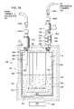
- FIG. 7Aillustrates a sectional view of a canister surrounded by a canister heater in accordance with one embodiment of the invention
- FIG. 7Billustrates a sectional view of a canister surrounded by a canister heater in accordance with another embodiment of the invention.
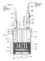
- FIG. 8illustrates a sectional view of a canister containing a plurality of solid particles in accordance with one embodiment of the invention.
- FIG. 1is a schematic cross-sectional view of one embodiment of a substrate 100 having a dielectric layer 102 and a barrier layer 104 deposited thereon.
- the substrate 100may be a silicon semiconductor substrate, or other material layer, which has been formed on the substrate.
- the dielectric layer 102may be an oxide, a silicon oxide, carbon-silicon-oxide, a fluoro-silicon, a porous dielectric, or other suitable dielectric formed and patterned to provide a contact hole or via 102 H extending to an exposed surface portion 102 T of the substrate 100 .
- the substrate 100refers to any work piece upon which film processing is performed, and a substrate structure 150 is used to denote the substrate 100 as well as other material layers formed on the substrate 100 , such as the dielectric layer 102 . It is also understood by those with skill in the art that the present invention may be used in a dual damascene process flow.
- the barrier layer 104is formed over the substrate structure 150 of FIG. 1A by atomic layer deposition (ALD).
- the barrier layerincludes a tantalum nitride layer.
- atomic layer deposition of a tantalum nitride barrier layerincludes sequentially providing a tantalum containing compound and a nitrogen-containing compound to a process chamber. Sequentially providing a tantalum containing compound and a nitrogen-containing compound may result in the alternating chemisorption of monolayers of a tantalum-containing compound and of monolayers of a nitrogen-containing compound on the substrate structure 150 .
- FIGS. 2A-2Cillustrate one embodiment of the alternating chemisorption of monolayers of a tantalum containing compound and a nitrogen containing compound on an exemplary portion of substrate 200 in a stage of integrated circuit fabrication, and more particularly at a stage of barrier layer formation.
- a monolayer of a tantalum containing compoundis chemisorbed on the substrate 200 by introducing a pulse of the tantalum containing compound 205 into a process chamber.
- the tantalum containing compound 205typically includes tantalum atoms 210 with one or more reactive species 215 .
- the tantalum containing compoundis pentakis(dimethylamido)tantalum (PDMAT; Ta(NMe 2 ) 5 ).
- PDMATmay be advantageously used for a number of reasons. PDMAT is relatively stable. In addition, PDMAT has an adequate vapor pressure which makes it easy to deliver. In particular, PDMAT may be produced with a low halide content. The halide content of PDMAT should be produced with a halide content of less than 100 ppm. Not wishing to be bound by theory, it is believed that an organometallic precursor with a low halide content is beneficial because halogens (such as chlorine) incorporated in the barrier layer may attack the copper layer deposited thereon.
- halogenssuch as chlorine
- Thermal decomposition of the PDMAT during productionmay cause impurities in the PDMAT product, which is subsequently used to form the tantalum nitride barrier layer.
- the impuritiesmay include compounds such as CH 3 NTa(N(CH 3 ) 2 ) 3 and ((CH 3 ) 2 N) 3 Ta(NCH 2 CH 3 ).
- reactions with moisturemay result in tantalum oxo amide compounds in the PDMAT product.
- the tantalum oxo amide compoundsare removed from the PDMAT by sublimation.
- the tantalum oxo amide compoundsare removed in a bubbler.
- the PDMAT productpreferably has less than about 5 ppm of chlorine.
- the levels of lithium, iron, fluorine, bromine, and iodineshould be minimized.
- the total level of impuritiesis less than about 5 ppm.
- the tantalum containing compoundmay be provided as a gas or may be provided with the aid of a carrier gas.
- carrier gaseswhich may be used include, but are not limited to, helium (He), argon (Ar), nitrogen (N 2 ), and hydrogen (H 2 ).
- tantalum containing compoundAfter the monolayer of the tantalum containing compound is chemisorbed onto the substrate 200 , excess tantalum containing compound is removed from the process chamber by introducing a pulse of a purge gas thereto.
- purge gaseswhich may be used include, but are not limited to, helium (He), argon (Ar), nitrogen (N 2 ), hydrogen (H 2 ), and other gases.
- a pulse of a nitrogen containing compound 225is introduced into the process chamber.
- the nitrogen containing compound 225may be provided alone or may be provided with the aid of a carrier gas.
- the nitrogen containing compound 225may comprise nitrogen atoms 230 with one or more reactive species 235 .
- the nitrogen containing compoundpreferably includes ammonia gas (NH 3 ).
- nitrogen containing compoundsmay be used which include, but are not limited to, N x H y with x and y being integers (e.g., hydrazine (N 2 H 4 )), dimethyl hydrazine ((CH 3 ) 2 N 2 H 2 ), t-butylhydrazine (C 4 H 9 N 2 H 3 ), phenylhydrazine (C 6 H 5 N 2 H 3 ), other hydrazine derivatives, a nitrogen plasma source (e.g., N 2 , N 2 /H 2 , NH 3 , or a N 2 H 4 plasma), 2,2′-azotertbutane ((CH 3 ) 6 C 2 N 2 ), ethylazide (C 2 H 5 N 3 ), and other suitable gases.
- a carrier gasmay be used to deliver the nitrogen containing compound if necessary.
- a monolayer of the nitrogen containing compound 225may be chemisorbed on the monolayer of the tantalum containing compound 205 .
- the composition and structure of precursors on a surface during atomic layer deposition (ALD)is not precisely known. Not wishing to be bound by theory, it is believed that the chemisorbed monolayer of the nitrogen containing compound 225 reacts with the monolayer of the tantalum containing compound 205 to form a tantalum nitride layer 209 .
- the reactive species 215 , 235form by-products 240 that are transported from the substrate surface by the vacuum system.
- any excess nitrogen containing compoundis removed from the process chamber by introducing another pulse of the purge gas therein.
- the tantalum nitride layer deposition sequence of alternating chemisorption of monolayers of the tantalum containing compound and of the nitrogen containing compoundmay be repeated, if necessary, until a desired tantalum nitride thickness is achieved.
- the tantalum nitride layer formationis depicted as starting with the chemisorption of a monolayer of a tantalum containing compound on the substrate followed by a monolayer of a nitrogen containing compound.
- the tantalum nitride layer formationmay start with the chemisorption of a monolayer of a nitrogen containing compound on the substrate followed by a monolayer of the tantalum containing compound.
- a pump evacuation alone between pulses of reactant gasesmay be used to prevent mixing of the reactant gases.
- the time duration for each pulse of the tantalum containing compound, the nitrogen containing compound, and the purge gasis variable and depends on the volume capacity of a deposition chamber employed as well as a vacuum system coupled thereto. For example, (1) a lower chamber pressure of a gas will require a longer pulse time; (2) a lower gas flow rate will require a longer time for chamber pressure to rise and stabilize requiring a longer pulse time; and (3) a large-volume chamber will take longer to fill and will take longer for chamber pressure to stabilize thus requiring a longer pulse time. Similarly, time between each pulse is also variable and depends on volume capacity of the process chamber as well as the vacuum system coupled thereto.
- the time duration of a pulse of the tantalum containing compound or the nitrogen containing compoundshould be long enough for chemisorption of a monolayer of the compound.
- the pulse time of the purge gasshould be long enough to remove the reaction by-products and/or any residual materials remaining in the process chamber.
- a pulse time of about 1.0 second or less for a tantalum containing compound and a pulse time of about 1.0 second or less for a nitrogen containing compoundare typically sufficient to chemisorb alternating monolayers on a substrate.
- a pulse time of about 1.0 second or less for a purge gasis typically sufficient to remove reaction by-products as well as any residual materials remaining in the process chamber.
- a longer pulse timemay be used to ensure chemisorption of the tantalum containing compound and the nitrogen containing compound and to ensure removal of the reaction by-products.
- the substratemay be maintained approximately below a thermal decomposition temperature of a selected tantalum containing compound.
- An exemplary heater temperature range to be used with tantalum containing compounds identified hereinis approximately between about 20° C. and about 500° C. at a chamber pressure less than about 100 Torr, preferably less than 50 Torr.
- the heater temperatureis preferably between about 100° C. and about 300° C., more preferably between about 175° C. and 250° C. In other embodiments, it should be understood that other temperatures may be used. For example, a temperature above a thermal decomposition temperature may be used.
- the temperatureshould be selected so that more than 50 percent of the deposition activity is by chemisorption processes.
- a temperature above a thermal decomposition temperaturemay be used in which the amount of decomposition during each precursor deposition is limited so that the growth mode will be similar to an atomic layer deposition growth mode.
- One exemplary process of depositing a tantalum nitride layer by atomic layer deposition in a process chamberincludes sequentially providing pentakis(dimethylamido)tantalum (PDMAT) at a flow rate between about 100 sccm (standard cubic centimeters per minute) and about 1,000 sccm, and preferably between about 200 sccm and 500 sccm, for a time period of about 1.0 second or less, providing ammonia at a flow rate between about 100 sccm and about 1,000 sccm, preferably between about 200 sccm and 500 sccm, for a time period of about 1.0 second or less, and a purge gas at a flow rate between about 100 sccm and about 1,000 sccm, preferably between about 200 sccm and 500 sccm for a time period of about 1.0 second or less.
- PDMATpentakis(dimethylamido)tantalum
- the heater temperaturepreferably is maintained between about 100° C. and about 300° C. at a chamber pressure between about 1.0 and about 5.0 Torr. This process provides a tantalum nitride layer in a thickness between about 0.5 ⁇ and about 1.0 ⁇ per cycle. The alternating sequence may be repeated until a desired thickness is achieved.
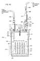
- FIG. 3is a schematic cross-sectional view of one exemplary embodiment of a processing system 320 that may be used to form one or more barrier layers by atomic layer deposition in accordance with aspects of the present invention.
- a processing system 320may be used to form one or more barrier layers by atomic layer deposition in accordance with aspects of the present invention.
- other processing systemsmay also be used.
- the processing system 320generally includes a processing chamber 306 coupled to a gas delivery system 304 .
- the processing chamber 306may be any suitable processing chamber, for example, those available from Applied Materials, Inc., located in Santa Clara, Calif. Exemplary processing chambers include DPS CENTURA® etch chambers, PRODUCER® chemical vapor deposition chambers, and ENDURA® physical vapor deposition chambers, among others.
- the gas delivery system 304generally controls the rate and pressure at which various process and inert gases are delivered to the processing chamber 306 .
- the number and types of process and other gases delivered to the processing chamber 306are generally selected based on the process to be performed in the processing chamber 306 coupled thereto. Although for simplicity a single gas delivery circuit is depicted in the gas delivery system 304 shown in FIG. 3 , it is contemplated that additional gas delivery circuits may be utilized.
- the gas delivery system 304is generally coupled between a carrier gas source 302 and the processing chamber 306 .
- the carrier gas source 302may be a local or remote vessel or a centralized facility source that supplies the carrier gas throughout the facility.
- the carrier gas source 302typically supplies a carrier gas such as argon, nitrogen, helium, or other inert or non-reactive gas.
- the gas delivery system 304typically includes a flow controller 310 coupled between the carrier gas source 302 and a process gas source canister 300 .
- the flow controller 310may be a proportional valve, modulating valve, needle valve, regulator, mass flow controller or the like.
- One flow controller 310 that may be utilizedis available from Sierra Instruments, Inc., located in Monterey, Calif.
- the source canister 300is typically coupled to and located between a first and a second valve 312 , 314 .
- the first and second valves 312 , 314are coupled to the source canister 300 and fitted with disconnect fittings (not shown) to facilitate removal of the valves 312 , 314 with the source canister 300 from the gas delivery system 304 .
- a third valve 316is disposed between the second valve 314 and the processing chamber 306 to prevent introduction of contaminates into the processing chamber 306 after removal of the source canister 300 from the gas delivery system 304 .
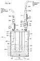
- FIGS. 4A-4Cdepict sectional views of embodiments of the source canister 300 .
- the source canister 300generally comprises an ampoule or other sealed container having a housing 420 that is adapted to hold precursor materials 414 from which a process (or other) gas may be generated through a sublimation or vaporization process.
- precursor materials 414that may generate a process gas in the source canister 300 through a sublimation process include xenon difluoride, nickel carbonyl, tungsten hexacarbonyl, and pentakis(dimethylamido) tantalum (PDMAT), among others.
- PDMATpentakis(dimethylamido) tantalum
- Some liquid precursor materials 414 that may generate a process gas in the source canister 300 through a vaporization processinclude tetrakis(dimethylamido) titanium (TDMAT), tertbutylimido tris(diethylamido)tantalum (TBTDET), and pentakis(ethylmethylamido)tantalum (PEMAT), among others.
- the housing 420is generally fabricated from a material substantially inert to the precursor materials 414 and gas produced therefrom, and thus, the material of construction may vary based on gas being produced.
- the housing 420may have any number of geometric forms.
- the housing 420comprises a cylindrical sidewall 402 and a bottom 432 sealed by a lid 404 .
- the lid 404may be coupled to the sidewall 402 by welding, bonding, adhesives, or other leak-tight method.
- the joint between the sidewall 402 and the lid 404may have a seal, o-ring, gasket, or the like, disposed therebetween to prevent leakage from the source canister 300 .
- the sidewall 402may alternatively comprise other hollow geometric forms, for example, a hollow square tube.
- An inlet port 406 and an outlet port 408are formed through the source canister to allow gas flow into and out of the source canister 300 .
- the ports 406 , 408may be formed through the lid 404 and/or sidewall 402 of the source canister 300 .
- the ports 406 , 408are generally sealable to allow the interior of the source canister 300 to be isolated from the surrounding environment during removal of the source canister 300 from the gas delivery system 304 .
- valves 312 , 314are sealingly coupled to ports 406 , 408 to prevent leakage from the source canister 300 when removed from the gas delivery system 304 (shown in FIG. 3 ) for recharging of the precursor material 414 or replacement of the source canister 300 .
- Mating disconnect fittings 436 A, 436 Bmay be coupled to valves 312 , 314 to facilitate removal and replacement of the source canister 300 to and from the gas delivery system 304 .
- Valves 312 , 314are typically ball valves or other positive sealing valves that allow the source canister 300 to be removed from the system efficiently loaded and recycled while minimizing potential leakage from the source canister 300 during filling, transport, or coupling to the gas delivery system 304 .
- the source canister 300can be refilled through a refill port 460 such as a small tube 464 with a VCR fitting 462 disposed on the lid 404 of the source canister 300 , as depicted in FIG. 4C .
- the source canister 300has an interior volume 438 having an upper region 418 and a lower region 434 .
- the lower region 434 of source canister 300is at least partially filled with the precursor materials 414 .
- a liquid 416may be added to a solid precursor material 414 to form a slurry 412 .
- the precursor materials 414 , the liquid 416 , or the premixed slurry 412may be introduced into source canister 300 by removing the lid 404 or through one of the ports 406 , 408 .
- the liquid 416is selected such that the liquid 416 is non-reactive with the precursor materials 414 , that the precursor materials 414 are insoluble therein, that the liquid 416 has a negligible vapor pressure compared to the precursor materials 414 , and that the ratio of the vapor pressure of the solid precursor material 414 , e.g., tungsten hexacarbonyl, to that of the liquid 416 is greater than 103.
- Precursor materials 414 mixed with the liquid 416may be sporadically agitated to keep the precursor materials 414 suspended in the liquid 416 in the slurry 412 .
- precursor materials 414 and the liquid 416are agitated by a magnetic stirrer 440 .
- the magnetic stirrer 440includes a magnetic motor 442 disposed beneath the bottom 432 of the source canister 300 and a magnetic pill 444 disposed in the lower region 434 of the source canister 300 .
- the magnetic motor 442operates to rotate the magnetic pill 444 within the source canister 300 , thereby mixing the slurry 412 .
- the magnetic pill 444should have an outer coating of material that is a non-reactive with the precursor materials 414 , the liquid 416 , or the source canister 300 .
- Suitable magnetic mixersare commercially available.
- One example of a suitable magnetic mixeris IKAMAG® REO available from IKA® Works in Wilmington, N.C.
- the slurry 412may be agitated other means, such as by a mixer, a bubbler, or the like.
- the agitation of the liquid 416may induce droplets of the liquid 416 to become entrained in the carrier gas and carried toward the processing chamber 306 .
- an oil trap 450may optionally be coupled to the exit port 408 of the source canister 300 .
- the oil trap 450includes a body 452 containing a plurality of interleaved baffles 454 which extend past a centerline 456 of the oil trap body 452 and are angled at least slightly downward towards the source canister 300 .
- the baffles 454force the gas flowing towards the processing chamber 306 to flow a tortuous path around the baffles 454 .
- the surface area of the baffles 454provides a large surface area exposed to the flowing gas to which oil droplets that may be entrained in the gas adhere.
- the downward angle of the baffles 454allows any oil accumulated in the oil trap to flow downward and back into the source canister 300 .
- the source canister 300includes at least one baffle 410 disposed within the upper region 418 of the source canister 300 , per one embodiment depicted in FIG. 4A .
- the baffle 410is disposed between inlet port 406 and outlet port 408 , creating an extended mean flow path, thereby preventing direct (i.e., straight line) flow of the carrier gas from the inlet port 406 to the outlet port 408 . This has the effect of increasing the mean dwell time of the carrier gas in the source canister 300 and increasing the quantity of sublimated or vaporized precursor gas carried by the carrier gas.
- the baffles 410direct the carrier gas over the entire exposed surface of the precursor material 414 disposed in the source canister 300 , ensuring repeatable gas generation characteristics and efficient consumption of the precursor material 414 .
- the number, spacing, and shape of the baffles 410may be selected to tune the source canister 300 for optimum generation of precursor gas. For example, a greater number of baffles 410 may be selected to impart higher carrier gas velocities at the precursor material 414 or the shape of the baffles 410 may be configured to control the consumption of the precursor material 414 for more efficient usage of the precursor material.
- the baffle 410may be attached to the sidewall 402 ( FIG. 4B ), the lid 404 ( FIG. 4A ), or the baffle 410 may be a prefabricated insert 413 designed to fit within the source canister 300 ( FIG. 4C ).
- the baffles 410 disposed in the source canister 300comprise five rectangular plates fabricated of the same material as the sidewall 402 . Referring to FIG. 4B , the baffles 410 are welded or otherwise fastened to the sidewall 402 parallel to each other. The baffles 410 are interleaved, fastened to opposing sides of the source canister in an alternating fashion, such that a serpentine extended mean flow path is created.
- baffles 410are situated between the inlet port 406 and the outlet port 408 on the lid 404 when placed on the sidewall 402 and are disposed such that there is no air space between the baffles 410 and the lid 404 .
- the baffles 410additionally extend at least partially into the lower region 434 of the source canister 300 , thus defining an extended mean flow path for the carrier gas flowing through the upper region 418 .
- an inlet tube 422may be disposed in the interior volume 438 of the source canister 300 .
- the tube 422is coupled by a first end 424 to the inlet port 406 of the source canister 300 and terminates at a second end 426 in the upper region 418 of the source canister 300 .
- the tube 422injects the carrier gas into the upper region 418 of the source canister 300 at a location closer to the precursor materials 414 or the slurry 412 .
- the precursor materials 414generate a precursor gas at a predefined temperature and pressure. Sublimating or vaporized gas from the precursor materials 414 accumulate in the upper region 418 of the source canister 300 and are swept out by an inert carrier gas entering through inlet port 406 and exiting outlet port 408 to be carried to the processing chamber 306 . In one embodiment, the precursor materials 414 are heated to a predefined temperature by a resistive heater 430 disposed proximate to the sidewall 402 .
- the precursor materials 414may be heated by other means, such as by a cartridge heater (not shown) disposed in the upper region 418 or the lower region 434 of the source canister 300 or by preheating the carrier gas with a heater (not shown) placed upstream of the carrier gas inlet port 406 .
- a cartridge heaternot shown
- the liquid 416 and the baffles 410should be good conductors of heat.
- a plurality of solid beads or particles 810 with high thermal conductivitysuch as, aluminum nitride or boron nitride, may be used in lieu of the liquid 416 , as shown in FIG. 8 .
- Such solid particles 810may be used to transfer more heat from the sidewall of the canister 800 to the precursor materials 414 than the liquid 416 .
- the solid particles 810have the same properties as the liquid 416 in that they are non-reactive with the precursor materials 414 , insoluble, have a negligible vapor pressure compared to the precursor materials 414 .
- the solid particles 810are configured to efficiently transfer heat from the sidewall of the canister 800 to the center portion of the canister 800 , thereby leading to more precursor material utilization during sublimation or vaporization.
- the solid particles 810may also be degassed and cleaned from contaminants, water vapor and the like, prior to being deposited into the canister 800 .
- the lower region 434 of the source canister 300is at least partially filled with a mixture of tungsten hexacarbonyl and diffusion pump oil to form the slurry 412 .
- the slurry 412is held at a pressure of about 5 Torr and is heated to a temperature in the range of about 40° C. to about 50° C. by a resistive heater 430 located proximate to the source canister 300 .
- Carrier gas in the form of argonis flowed through inlet port 406 into the upper region 418 at a rate of about 400 sccm.
- the argonflows in an extended mean flow path defined by the torturous path through the baffles 410 before exiting the source canister 300 through outlet port 408 , advantageously increasing the mean dwell time of the argon in the upper region 418 of the source canister 300 .
- the increased dwell time in the source canister 300advantageously increases the saturation level of sublimated tungsten hexacarbonyl vapors within the carrier gas.
- the torturous path through the baffles 410advantageously exposes the substantially all of the exposed surface area of the precursor material 414 to the carrier gas flow for uniform consumption of the precursor material 414 and generation of the precursor gas.
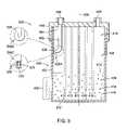
- FIGS. 7A-7Billustrate other embodiments for heating the precursor materials 414 . More specifically, FIGS. 7A-7B illustrate a sectional view of a canister 700 surrounded by a canister heater 730 , which is configured to create a temperature gradient between a lower region 434 of the canister 700 and an upper region 418 of the canister 700 with the lower region 434 being the coldest region and the upper region 418 being the hottest region.
- the temperature gradientmay range from about 5° C. to about 15° C.
- the canister heater 730is configured to ensure that the solid precursor materials 414 will accumulate at the lower region 434 of the canister 700 , thereby increasing the predictability of where the solid precursor materials 414 will condense and the temperature of the solid precursor materials 414 .
- the canister heater 730includes a heating element 750 disposed inside the canister heater 730 such that the entire canister 700 , including the upper region 418 and the lower region 434 , is heated by the canister heater 730 .
- the heating element 750 near the upper region 418may be configured to generate more heat than the heating element 750 near the lower region 434 , thereby allowing the canister heater 730 to create the temperature gradient between the lower region 434 and the upper region 418 .
- the heating element 750is configured such that the temperature at the upper region 418 is between about 5° C. to about 15° C. higher than the temperature at the lower region 434 .
- the heating element 750is configured such that the temperature at the upper region 418 is about 70° C., the temperature at the lower region 434 is about 60° C. and the temperature at the sidewall of the canister 700 is about 65° C.
- the power of the heating element 730may be about 600 watts at 208 VAC input.
- the canister heater 730may also include a cooling plate positioned at the bottom of the canister heater 730 to further ensure that the coldest region of the canister 700 is the lower region 434 , and thereby ensuring that the solid precursor materials 414 condense at the lower region 434 .
- the valves 312 , 314 , the oil trap 450 , the inlet port 406 and the exit port 408may be heated with a resistive heating tape. Since the upper region 418 is configured to have a higher temperature than the lower region 434 , the baffles 410 may be used to transfer heat from the upper region 418 to the lower region 434 , thereby allowing the canister heater 730 to maintain the desired temperature gradient.
- Embodiments of the inventionalso contemplate other heat transfer mediums, such as, silos 710 extending from the bottom portion 432 of the canister 700 to the upper region 418 , as depicted in FIG. 7B .
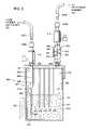
- FIG. 5depicts a sectional view of another embodiment of a canister 500 for generating a process gas.
- the canister 500includes a sidewall 402 , a lid 404 and a bottom 432 enclosing an interior volume 438 . At least one of the lid 404 or sidewall 402 contains an inlet port 406 and an outlet port 408 for gas entry and egress.
- the interior volume 438 of the canister 500is split into an upper region 418 and a lower region 434 .
- Precursor materials 414at least partially fill the lower region 434 .
- the precursor materials 414may be in the form of a solid, liquid, or slurry, and are adapted to generate a process gas by sublimation and/or vaporization.
- a tube 502is disposed in the interior volume 438 of the canister 500 and is adapted to direct a flow of gas within the canister 500 away from the precursor materials 414 , advantageously preventing gas flowing out of the tube 502 from directly impinging the precursor materials 414 and causing particulates to become airborne and carried through the outlet port 408 and into the processing chamber 306 .
- the tube 502is coupled at a first end 504 to the inlet port 406 .
- the tube 502extends from the first end 504 to a second end 526 A that is positioned in the upper region 418 above the precursor materials 414 .
- the second end 526 Amay be adapted to direct the flow of gas toward the sidewall 402 , thus preventing direct (linear or line of sight) flow of the gas through the canister 500 between the ports 406 , 408 , creating an extended mean flow path.
- an outlet 506 of the second end 526 A of the tube 502is oriented at an angle of about 15° to about 90° relative to a center axis 508 of the canister 500 .
- the tube 502has a ‘J’-shaped second end 526 B that directs the flow of gas exiting the outlet 506 towards the lid 404 of the canister 500 .
- the tube 502has a capped second end 526 C having a plug or cap 510 closing the end of the tube 502 .
- the capped second end 526 Chas at least one opening 528 formed in the side of the tube 502 proximate the cap 510 .
- Gas, exiting the openings 528is typically directed perpendicular to the center axis 508 and away from the precursor materials 414 disposed in the lower region 434 of the canister 500 .
- at least one baffle 410(shown in phantom) as described above may be disposed within the chamber 500 and utilized in tandem with any of the embodiments of the tube 502 described above.
- the lower region 434 of the canister 500is at least partially filled with a mixture of tungsten hexacarbonyl and diffusion pump oil to form the slurry 412 .
- the slurry 412is held at a pressure of about 5 Torr and is heated to a temperature in the range of about 40° C. to about 50° C. by a resistive heater 430 located proximate to the canister 500 .
- a carrier gas in the form of argonis flowed through the inlet port 406 and the tube 502 into the upper region 418 at a rate of about 200 sccm.
- the second end 526 A of the tube 502directs the flow of the carrier gas in an extended mean flow path away from the outlet port 408 , advantageously increasing the mean dwell time of the argon in the upper region 418 of the canister 500 and preventing direct flow of carrier gas upon the precursor materials 414 to minimize particulate generation.
- the increased dwell time in the canister 500advantageously increases the saturation level of sublimated tungsten hexacarbonyl gas within the carrier gas while the decrease in particulate generation improves product yields, conserves source solids, and reduces downstream contamination.
- FIG. 6depicts a sectional view of another embodiment of a canister 600 for generating a precursor gas.
- the canister 600includes a sidewall 402 , a lid 404 , and a bottom 432 enclosing an interior volume 438 .
- At least one of the lid 404 or sidewall 402contains an inlet port 406 and an outlet port 408 for gas entry and egress.
- Inlet and outlet ports 406 , 408are coupled to valves 312 , 314 fitted with mating disconnect fittings 436 A, 436 B to facilitate removal of the canister 600 from the gas delivery system 304 .
- an oil trap 450is coupled between the outlet port 408 and the valve 314 to capture any oil particulate that may be present in the gas flowing to the process chamber 306 .
- the interior volume 438 of the canister 600is split into an upper region 418 and a lower region 434 .
- Precursor materials 414 and a liquid 416at least partially fill the lower region 434 .
- a tube 602is disposed in the interior volume 438 of the canister 600 and is adapted to direct a first gas flow F 1 within the canister 600 away from the precursor material and liquid mixture and to direct a second gas flow F 2 through the mixture.
- the flow F 1is much greater than the flow F 2 .
- the flow F 2is configured to act as a bubbler, being great enough to agitate the precursor material and liquid mixture but not enough to cause particles or droplets of the precursor materials 414 or liquid 416 from becoming airborne.
- this embodimentadvantageously agitates the precursor material and liquid mixture while minimizing particulates produced due to direct impingement of the gas flowing out of the tube 602 on the precursor materials 414 from becoming airborne and carried through the outlet port 408 and into the processing chamber 306 .
- the tube 602is coupled at a first end 604 to the inlet port 406 .
- the tube 602extends from the first end 604 to a second end 606 that is positioned in the lower region 434 of the canister 600 , within the precursor material and liquid mixture.
- the tube 602has an opening 608 disposed in the upper region 418 of the canister 600 that directs the first gas flow F 1 towards a sidewall 402 of the canister 600 .
- the tube 600has a restriction 610 disposed in the upper region 438 of the canister 600 located below the opening 608 .
- the restriction 610serves to decrease the second gas flow F 2 flowing toward the second end 606 of the tube 602 and into the slurry 412 .
- the relative rates of the first and second gas flows F 1 and F 2can be regulated.
- This regulationserves at least two purposes.
- the second gas flow F 2can be minimized to provide just enough agitation to maintain suspension or mixing of the precursor materials 414 in the liquid 416 while minimizing particulate generation and potential contamination of the processing chamber 306 .
- the first gas flow F 1can be regulated to maintain the overall flow volume necessary to provide the required quantity of sublimated and/or vapors from the precursor materials 414 to the processing chamber 306 .
- an at least one baffle 410 as described abovemay be disposed within the canister 600 and utilized in tandem with any of the embodiments of the tube 602 described above.
Landscapes
- Chemical & Material Sciences (AREA)
- Engineering & Computer Science (AREA)
- Chemical Kinetics & Catalysis (AREA)
- General Chemical & Material Sciences (AREA)
- Materials Engineering (AREA)
- Mechanical Engineering (AREA)
- Metallurgy (AREA)
- Organic Chemistry (AREA)
- Inorganic Chemistry (AREA)
- Physics & Mathematics (AREA)
- Condensed Matter Physics & Semiconductors (AREA)
- General Physics & Mathematics (AREA)
- Manufacturing & Machinery (AREA)
- Computer Hardware Design (AREA)
- Microelectronics & Electronic Packaging (AREA)
- Power Engineering (AREA)
- Chemical Vapour Deposition (AREA)
Abstract
Description
This application is a continuation of U.S. Ser. No. 11/119,681, filed May 2, 2005, now U.S. Pat. No. 7,270,709, which is a continuation of U.S. Ser. No. 10/447,255, filed May 27, 2003, issued as U.S. Pat. No. 6,905,541, which is a continuation-in-part of U.S. Ser. No. 10/198,727, filed Jul. 17, 2002, now. U.S. Patent No. 7,186,385, which are all incorporated herein by reference in their entirety.
1. Field of the Invention
Embodiments of the invention generally relate to apparatuses and processes for generating a chemical precursor that may be used during a vapor deposition process.
2. Description of the Related Art
Reliably producing sub-micron and smaller features is one of the key technologies for the next generation of very large scale integration (VLSI) and ultra large scale integration (ULSI) of semiconductor devices. However, as the fringes of circuit technology are pressed, the shrinking dimensions of interconnects in VLSI and ULSI technology have placed additional demands on the processing capabilities. The multilevel interconnects that lie at the heart of this technology require precise processing of high aspect ratio features, such as vias and other interconnects. Reliable formation of these interconnects is very important to VLSI and ULSI success and to the continued effort to increase circuit density and quality of individual substrates.
As circuit densities increase, the widths of vias, contacts and other features, as well as the dielectric materials between them, decrease to sub-micron dimensions (e.g., about 0.20 micrometers or less), whereas the thickness of the dielectric layers remains substantially constant, with the result that the aspect ratios for the features, i.e., their height divided by width, increase. Many traditional deposition processes have difficulty filling sub-micron structures where the aspect ratio exceeds 4:1, and particularly where the aspect ratio exceeds 10:1. Therefore, there is a great amount of ongoing effort being directed at the formation of substantially void-free and seam-free sub-micron features having high aspect ratios.
Currently, copper and its alloys have become the metals of choice for sub-micron interconnect technology because copper has a lower resistivity than aluminum, (about 1.7 μΩ-cm compared to about 3.1 μΩ-cm for aluminum), and a higher current carrying capacity and significantly higher electromigration resistance. These characteristics are important for supporting the higher current densities experienced at high levels of integration and increased device speed. Further, copper has a good thermal conductivity and is available in a highly pure state.
Copper metallization can be achieved by a variety of techniques. A typical method generally includes physical vapor depositing a barrier layer over a feature, physical vapor depositing a copper seed layer over the barrier layer, and then electroplating a copper conductive material layer over the copper seed layer to fill the feature. Finally, the deposited layers and the dielectric layers are planarized, such as by chemical mechanical polishing (CMP), to define a conductive interconnect feature.
However, one problem with the use of copper is that copper diffuses into silicon, silicon dioxide, and other dielectric materials which may compromise the integrity of devices. Therefore, conformal barrier layers become increasingly important to prevent copper diffusion. Tantalum nitride has been used as a barrier material to prevent the diffusion of copper into underlying layers. However, the chemicals used in the barrier layer deposition, such as pentakis(dimethylamido)tantalum (PDMAT; Ta[N(CH3)2]5), may include impurities that cause defects in the fabrication of semiconductor devices and reduce process yields. Therefore, there exists a need for a method of depositing a barrier layer from a high-purity precursor.
Embodiments of the present invention include a method for filling a feature in a substrate. In one embodiment, the method includes depositing a barrier layer formed from purified pentakis(dimethylamido)tantalum having less than about 5 ppm of chlorine. The method additionally may include depositing a seed layer over the barrier layer and depositing a conductive layer over the seed layer.
Embodiments of the present invention further include a canister for vaporizing PDMAT prior to depositing a tantalum nitride layer on a substrate. The canister includes a sidewall, a top portion and a bottom portion. The canister contains an interior volume having an upper region and a lower region. A heater surrounds the canister, in which the heater creates a temperature gradient between the upper region and the lower region.
Embodiments of the present invention further include purified pentakis(dimethylamido)tantalum having less than about 5 ppm of chlorine.
So that the manner in which the above recited features of the present invention are attained and can be understood in detail, a more particular description of the invention, briefly summarized above, may be had by reference to the embodiments thereof, which are illustrated in the appended drawings. It is to be noted, however, that the appended drawings illustrate only typical embodiments of this invention, and are therefore, not to be considered limiting of its scope, for the invention may admit to other equally effective embodiments.
In one aspect, atomic layer deposition of a tantalum nitride barrier layer includes sequentially providing a tantalum containing compound and a nitrogen-containing compound to a process chamber. Sequentially providing a tantalum containing compound and a nitrogen-containing compound may result in the alternating chemisorption of monolayers of a tantalum-containing compound and of monolayers of a nitrogen-containing compound on thesubstrate structure 150.
Thetantalum containing compound 205 typically includestantalum atoms 210 with one or morereactive species 215. In one embodiment, the tantalum containing compound is pentakis(dimethylamido)tantalum (PDMAT; Ta(NMe2)5). PDMAT may be advantageously used for a number of reasons. PDMAT is relatively stable. In addition, PDMAT has an adequate vapor pressure which makes it easy to deliver. In particular, PDMAT may be produced with a low halide content. The halide content of PDMAT should be produced with a halide content of less than 100 ppm. Not wishing to be bound by theory, it is believed that an organometallic precursor with a low halide content is beneficial because halogens (such as chlorine) incorporated in the barrier layer may attack the copper layer deposited thereon.
Thermal decomposition of the PDMAT during production may cause impurities in the PDMAT product, which is subsequently used to form the tantalum nitride barrier layer. The impurities may include compounds such as CH3NTa(N(CH3)2)3and ((CH3)2N)3Ta(NCH2CH3). In addition, reactions with moisture may result in tantalum oxo amide compounds in the PDMAT product. Preferably, the tantalum oxo amide compounds are removed from the PDMAT by sublimation. For example, the tantalum oxo amide compounds are removed in a bubbler. The PDMAT product preferably has less than about 5 ppm of chlorine. In addition, the levels of lithium, iron, fluorine, bromine, and iodine should be minimized. Most preferably, the total level of impurities is less than about 5 ppm.
The tantalum containing compound may be provided as a gas or may be provided with the aid of a carrier gas. Examples of carrier gases which may be used include, but are not limited to, helium (He), argon (Ar), nitrogen (N2), and hydrogen (H2).
After the monolayer of the tantalum containing compound is chemisorbed onto thesubstrate 200, excess tantalum containing compound is removed from the process chamber by introducing a pulse of a purge gas thereto. Examples of purge gases which may be used include, but are not limited to, helium (He), argon (Ar), nitrogen (N2), hydrogen (H2), and other gases.
Referring toFIG. 2B , after the process chamber has been purged, a pulse of anitrogen containing compound 225 is introduced into the process chamber. Thenitrogen containing compound 225 may be provided alone or may be provided with the aid of a carrier gas. Thenitrogen containing compound 225 may comprisenitrogen atoms 230 with one or morereactive species 235. The nitrogen containing compound preferably includes ammonia gas (NH3). Other nitrogen containing compounds may be used which include, but are not limited to, NxHywith x and y being integers (e.g., hydrazine (N2H4)), dimethyl hydrazine ((CH3)2N2H2), t-butylhydrazine (C4H9N2H3), phenylhydrazine (C6H5N2H3), other hydrazine derivatives, a nitrogen plasma source (e.g., N2, N2/H2, NH3, or a N2H4plasma), 2,2′-azotertbutane ((CH3)6C2N2), ethylazide (C2H5N3), and other suitable gases. A carrier gas may be used to deliver the nitrogen containing compound if necessary.
A monolayer of thenitrogen containing compound 225 may be chemisorbed on the monolayer of thetantalum containing compound 205. The composition and structure of precursors on a surface during atomic layer deposition (ALD) is not precisely known. Not wishing to be bound by theory, it is believed that the chemisorbed monolayer of thenitrogen containing compound 225 reacts with the monolayer of thetantalum containing compound 205 to form atantalum nitride layer 209. Thereactive species products 240 that are transported from the substrate surface by the vacuum system.
After the monolayer of thenitrogen containing compound 225 is chemisorbed on the monolayer of the tantalum containing compound, any excess nitrogen containing compound is removed from the process chamber by introducing another pulse of the purge gas therein. Thereafter, as shown inFIG. 2C , the tantalum nitride layer deposition sequence of alternating chemisorption of monolayers of the tantalum containing compound and of the nitrogen containing compound may be repeated, if necessary, until a desired tantalum nitride thickness is achieved.
InFIGS. 2A-2C , the tantalum nitride layer formation is depicted as starting with the chemisorption of a monolayer of a tantalum containing compound on the substrate followed by a monolayer of a nitrogen containing compound. Alternatively, the tantalum nitride layer formation may start with the chemisorption of a monolayer of a nitrogen containing compound on the substrate followed by a monolayer of the tantalum containing compound. Furthermore, in an alternative embodiment, a pump evacuation alone between pulses of reactant gases may be used to prevent mixing of the reactant gases.
The time duration for each pulse of the tantalum containing compound, the nitrogen containing compound, and the purge gas is variable and depends on the volume capacity of a deposition chamber employed as well as a vacuum system coupled thereto. For example, (1) a lower chamber pressure of a gas will require a longer pulse time; (2) a lower gas flow rate will require a longer time for chamber pressure to rise and stabilize requiring a longer pulse time; and (3) a large-volume chamber will take longer to fill and will take longer for chamber pressure to stabilize thus requiring a longer pulse time. Similarly, time between each pulse is also variable and depends on volume capacity of the process chamber as well as the vacuum system coupled thereto. In general, the time duration of a pulse of the tantalum containing compound or the nitrogen containing compound should be long enough for chemisorption of a monolayer of the compound. In general, the pulse time of the purge gas should be long enough to remove the reaction by-products and/or any residual materials remaining in the process chamber.
Generally, a pulse time of about 1.0 second or less for a tantalum containing compound and a pulse time of about 1.0 second or less for a nitrogen containing compound are typically sufficient to chemisorb alternating monolayers on a substrate. A pulse time of about 1.0 second or less for a purge gas is typically sufficient to remove reaction by-products as well as any residual materials remaining in the process chamber. Of course, a longer pulse time may be used to ensure chemisorption of the tantalum containing compound and the nitrogen containing compound and to ensure removal of the reaction by-products.
During atomic layer deposition, the substrate may be maintained approximately below a thermal decomposition temperature of a selected tantalum containing compound. An exemplary heater temperature range to be used with tantalum containing compounds identified herein is approximately between about 20° C. and about 500° C. at a chamber pressure less than about 100 Torr, preferably less than 50 Torr. When the tantalum containing gas is PDMAT, the heater temperature is preferably between about 100° C. and about 300° C., more preferably between about 175° C. and 250° C. In other embodiments, it should be understood that other temperatures may be used. For example, a temperature above a thermal decomposition temperature may be used. However, the temperature should be selected so that more than 50 percent of the deposition activity is by chemisorption processes. In another example, a temperature above a thermal decomposition temperature may be used in which the amount of decomposition during each precursor deposition is limited so that the growth mode will be similar to an atomic layer deposition growth mode.
One exemplary process of depositing a tantalum nitride layer by atomic layer deposition in a process chamber includes sequentially providing pentakis(dimethylamido)tantalum (PDMAT) at a flow rate between about 100 sccm (standard cubic centimeters per minute) and about 1,000 sccm, and preferably between about 200 sccm and 500 sccm, for a time period of about 1.0 second or less, providing ammonia at a flow rate between about 100 sccm and about 1,000 sccm, preferably between about 200 sccm and 500 sccm, for a time period of about 1.0 second or less, and a purge gas at a flow rate between about 100 sccm and about 1,000 sccm, preferably between about 200 sccm and 500 sccm for a time period of about 1.0 second or less. The heater temperature preferably is maintained between about 100° C. and about 300° C. at a chamber pressure between about 1.0 and about 5.0 Torr. This process provides a tantalum nitride layer in a thickness between about 0.5 Å and about 1.0 Å per cycle. The alternating sequence may be repeated until a desired thickness is achieved.
Theprocessing system 320 generally includes aprocessing chamber 306 coupled to agas delivery system 304. Theprocessing chamber 306 may be any suitable processing chamber, for example, those available from Applied Materials, Inc., located in Santa Clara, Calif. Exemplary processing chambers include DPS CENTURA® etch chambers, PRODUCER® chemical vapor deposition chambers, and ENDURA® physical vapor deposition chambers, among others.
Thegas delivery system 304 generally controls the rate and pressure at which various process and inert gases are delivered to theprocessing chamber 306. The number and types of process and other gases delivered to theprocessing chamber 306 are generally selected based on the process to be performed in theprocessing chamber 306 coupled thereto. Although for simplicity a single gas delivery circuit is depicted in thegas delivery system 304 shown inFIG. 3 , it is contemplated that additional gas delivery circuits may be utilized.
Thegas delivery system 304 is generally coupled between acarrier gas source 302 and theprocessing chamber 306. Thecarrier gas source 302 may be a local or remote vessel or a centralized facility source that supplies the carrier gas throughout the facility. Thecarrier gas source 302 typically supplies a carrier gas such as argon, nitrogen, helium, or other inert or non-reactive gas.
Thegas delivery system 304 typically includes aflow controller 310 coupled between thecarrier gas source 302 and a processgas source canister 300. Theflow controller 310 may be a proportional valve, modulating valve, needle valve, regulator, mass flow controller or the like. Oneflow controller 310 that may be utilized is available from Sierra Instruments, Inc., located in Monterey, Calif.
Thesource canister 300 is typically coupled to and located between a first and asecond valve second valves source canister 300 and fitted with disconnect fittings (not shown) to facilitate removal of thevalves source canister 300 from thegas delivery system 304. Athird valve 316 is disposed between thesecond valve 314 and theprocessing chamber 306 to prevent introduction of contaminates into theprocessing chamber 306 after removal of thesource canister 300 from thegas delivery system 304.
Thehousing 420 may have any number of geometric forms. In the embodiment depicted inFIGS. 4A-4C , thehousing 420 comprises acylindrical sidewall 402 and a bottom432 sealed by alid 404. Thelid 404 may be coupled to thesidewall 402 by welding, bonding, adhesives, or other leak-tight method. Alternately, the joint between thesidewall 402 and thelid 404 may have a seal, o-ring, gasket, or the like, disposed therebetween to prevent leakage from thesource canister 300. Thesidewall 402 may alternatively comprise other hollow geometric forms, for example, a hollow square tube.
Aninlet port 406 and anoutlet port 408 are formed through the source canister to allow gas flow into and out of thesource canister 300. Theports lid 404 and/orsidewall 402 of thesource canister 300. Theports source canister 300 to be isolated from the surrounding environment during removal of thesource canister 300 from thegas delivery system 304. In one embodiment,valves ports source canister 300 when removed from the gas delivery system304 (shown inFIG. 3 ) for recharging of theprecursor material 414 or replacement of thesource canister 300.Mating disconnect fittings valves source canister 300 to and from thegas delivery system 304.Valves source canister 300 to be removed from the system efficiently loaded and recycled while minimizing potential leakage from thesource canister 300 during filling, transport, or coupling to thegas delivery system 304. Alternatively, thesource canister 300 can be refilled through arefill port 460 such as asmall tube 464 with a VCR fitting462 disposed on thelid 404 of thesource canister 300, as depicted inFIG. 4C .
Thesource canister 300 has aninterior volume 438 having anupper region 418 and alower region 434. Thelower region 434 ofsource canister 300 is at least partially filled with theprecursor materials 414. Alternately, a liquid416 may be added to asolid precursor material 414 to form aslurry 412. Theprecursor materials 414, the liquid416, or thepremixed slurry 412 may be introduced intosource canister 300 by removing thelid 404 or through one of theports precursor materials 414, that theprecursor materials 414 are insoluble therein, that the liquid416 has a negligible vapor pressure compared to theprecursor materials 414, and that the ratio of the vapor pressure of thesolid precursor material 414, e.g., tungsten hexacarbonyl, to that of the liquid416 is greater than 103.
The agitation of the liquid416 may induce droplets of the liquid416 to become entrained in the carrier gas and carried toward theprocessing chamber 306. To prevent such droplets of liquid416 from reaching theprocessing chamber 306, anoil trap 450 may optionally be coupled to theexit port 408 of thesource canister 300. Theoil trap 450 includes abody 452 containing a plurality of interleavedbaffles 454 which extend past acenterline 456 of theoil trap body 452 and are angled at least slightly downward towards thesource canister 300. Thebaffles 454 force the gas flowing towards theprocessing chamber 306 to flow a tortuous path around thebaffles 454. The surface area of thebaffles 454 provides a large surface area exposed to the flowing gas to which oil droplets that may be entrained in the gas adhere. The downward angle of thebaffles 454 allows any oil accumulated in the oil trap to flow downward and back into thesource canister 300.
Thesource canister 300 includes at least onebaffle 410 disposed within theupper region 418 of thesource canister 300, per one embodiment depicted inFIG. 4A . Thebaffle 410 is disposed betweeninlet port 406 andoutlet port 408, creating an extended mean flow path, thereby preventing direct (i.e., straight line) flow of the carrier gas from theinlet port 406 to theoutlet port 408. This has the effect of increasing the mean dwell time of the carrier gas in thesource canister 300 and increasing the quantity of sublimated or vaporized precursor gas carried by the carrier gas. Additionally, thebaffles 410 direct the carrier gas over the entire exposed surface of theprecursor material 414 disposed in thesource canister 300, ensuring repeatable gas generation characteristics and efficient consumption of theprecursor material 414.
The number, spacing, and shape of thebaffles 410 may be selected to tune thesource canister 300 for optimum generation of precursor gas. For example, a greater number ofbaffles 410 may be selected to impart higher carrier gas velocities at theprecursor material 414 or the shape of thebaffles 410 may be configured to control the consumption of theprecursor material 414 for more efficient usage of the precursor material.
Thebaffle 410 may be attached to the sidewall402 (FIG. 4B ), the lid404 (FIG. 4A ), or thebaffle 410 may be aprefabricated insert 413 designed to fit within the source canister300 (FIG. 4C ). In one embodiment, thebaffles 410 disposed in thesource canister 300 comprise five rectangular plates fabricated of the same material as thesidewall 402. Referring toFIG. 4B , thebaffles 410 are welded or otherwise fastened to thesidewall 402 parallel to each other. Thebaffles 410 are interleaved, fastened to opposing sides of the source canister in an alternating fashion, such that a serpentine extended mean flow path is created. Furthermore, thebaffles 410 are situated between theinlet port 406 and theoutlet port 408 on thelid 404 when placed on thesidewall 402 and are disposed such that there is no air space between thebaffles 410 and thelid 404. Thebaffles 410 additionally extend at least partially into thelower region 434 of thesource canister 300, thus defining an extended mean flow path for the carrier gas flowing through theupper region 418.
Optionally, aninlet tube 422 may be disposed in theinterior volume 438 of thesource canister 300. Thetube 422 is coupled by afirst end 424 to theinlet port 406 of thesource canister 300 and terminates at asecond end 426 in theupper region 418 of thesource canister 300. Thetube 422 injects the carrier gas into theupper region 418 of thesource canister 300 at a location closer to theprecursor materials 414 or theslurry 412.
Theprecursor materials 414 generate a precursor gas at a predefined temperature and pressure. Sublimating or vaporized gas from theprecursor materials 414 accumulate in theupper region 418 of thesource canister 300 and are swept out by an inert carrier gas entering throughinlet port 406 and exitingoutlet port 408 to be carried to theprocessing chamber 306. In one embodiment, theprecursor materials 414 are heated to a predefined temperature by aresistive heater 430 disposed proximate to thesidewall 402. Alternately, theprecursor materials 414 may be heated by other means, such as by a cartridge heater (not shown) disposed in theupper region 418 or thelower region 434 of thesource canister 300 or by preheating the carrier gas with a heater (not shown) placed upstream of the carriergas inlet port 406. To maximize uniform heat distribution throughout theslurry 412, the liquid416 and thebaffles 410 should be good conductors of heat.
In accordance with yet another embodiment of the invention, a plurality of solid beads orparticles 810 with high thermal conductivity, such as, aluminum nitride or boron nitride, may be used in lieu of the liquid416, as shown inFIG. 8 . Suchsolid particles 810 may be used to transfer more heat from the sidewall of thecanister 800 to theprecursor materials 414 than the liquid416. Thesolid particles 810 have the same properties as the liquid416 in that they are non-reactive with theprecursor materials 414, insoluble, have a negligible vapor pressure compared to theprecursor materials 414. As such, thesolid particles 810 are configured to efficiently transfer heat from the sidewall of thecanister 800 to the center portion of thecanister 800, thereby leading to more precursor material utilization during sublimation or vaporization. Thesolid particles 810 may also be degassed and cleaned from contaminants, water vapor and the like, prior to being deposited into thecanister 800.
In one exemplary mode of operation, thelower region 434 of thesource canister 300 is at least partially filled with a mixture of tungsten hexacarbonyl and diffusion pump oil to form theslurry 412. Theslurry 412 is held at a pressure of about 5 Torr and is heated to a temperature in the range of about 40° C. to about 50° C. by aresistive heater 430 located proximate to thesource canister 300. Carrier gas in the form of argon is flowed throughinlet port 406 into theupper region 418 at a rate of about 400 sccm. The argon flows in an extended mean flow path defined by the torturous path through thebaffles 410 before exiting thesource canister 300 throughoutlet port 408, advantageously increasing the mean dwell time of the argon in theupper region 418 of thesource canister 300. The increased dwell time in thesource canister 300 advantageously increases the saturation level of sublimated tungsten hexacarbonyl vapors within the carrier gas. Moreover, the torturous path through thebaffles 410 advantageously exposes the substantially all of the exposed surface area of theprecursor material 414 to the carrier gas flow for uniform consumption of theprecursor material 414 and generation of the precursor gas.
Thecanister heater 730 may also include a cooling plate positioned at the bottom of thecanister heater 730 to further ensure that the coldest region of thecanister 700 is thelower region 434, and thereby ensuring that thesolid precursor materials 414 condense at thelower region 434. Further, thevalves oil trap 450, theinlet port 406 and theexit port 408 may be heated with a resistive heating tape. Since theupper region 418 is configured to have a higher temperature than thelower region 434, thebaffles 410 may be used to transfer heat from theupper region 418 to thelower region 434, thereby allowing thecanister heater 730 to maintain the desired temperature gradient. Embodiments of the invention also contemplate other heat transfer mediums, such as,silos 710 extending from thebottom portion 432 of thecanister 700 to theupper region 418, as depicted inFIG. 7B .
Atube 502 is disposed in theinterior volume 438 of thecanister 500 and is adapted to direct a flow of gas within thecanister 500 away from theprecursor materials 414, advantageously preventing gas flowing out of thetube 502 from directly impinging theprecursor materials 414 and causing particulates to become airborne and carried through theoutlet port 408 and into theprocessing chamber 306. Thetube 502 is coupled at afirst end 504 to theinlet port 406. Thetube 502 extends from thefirst end 504 to asecond end 526A that is positioned in theupper region 418 above theprecursor materials 414. Thesecond end 526A may be adapted to direct the flow of gas toward thesidewall 402, thus preventing direct (linear or line of sight) flow of the gas through thecanister 500 between theports
In one embodiment, anoutlet 506 of thesecond end 526A of thetube 502 is oriented at an angle of about 15° to about 90° relative to acenter axis 508 of thecanister 500. In another embodiment, thetube 502 has a ‘J’-shapedsecond end 526B that directs the flow of gas exiting theoutlet 506 towards thelid 404 of thecanister 500. In another embodiment, thetube 502 has a cappedsecond end 526C having a plug or cap510 closing the end of thetube 502. The cappedsecond end 526C has at least oneopening 528 formed in the side of thetube 502 proximate thecap 510. Gas, exiting theopenings 528, is typically directed perpendicular to thecenter axis 508 and away from theprecursor materials 414 disposed in thelower region 434 of thecanister 500. Optionally, at least one baffle410 (shown in phantom) as described above may be disposed within thechamber 500 and utilized in tandem with any of the embodiments of thetube 502 described above.
In one exemplary mode of operation, thelower region 434 of thecanister 500 is at least partially filled with a mixture of tungsten hexacarbonyl and diffusion pump oil to form theslurry 412. Theslurry 412 is held at a pressure of about 5 Torr and is heated to a temperature in the range of about 40° C. to about 50° C. by aresistive heater 430 located proximate to thecanister 500. A carrier gas in the form of argon is flowed through theinlet port 406 and thetube 502 into theupper region 418 at a rate of about 200 sccm. Thesecond end 526A of thetube 502 directs the flow of the carrier gas in an extended mean flow path away from theoutlet port 408, advantageously increasing the mean dwell time of the argon in theupper region 418 of thecanister 500 and preventing direct flow of carrier gas upon theprecursor materials 414 to minimize particulate generation. The increased dwell time in thecanister 500 advantageously increases the saturation level of sublimated tungsten hexacarbonyl gas within the carrier gas while the decrease in particulate generation improves product yields, conserves source solids, and reduces downstream contamination.
Theinterior volume 438 of thecanister 600 is split into anupper region 418 and alower region 434.Precursor materials 414 and a liquid416 at least partially fill thelower region 434. Atube 602 is disposed in theinterior volume 438 of thecanister 600 and is adapted to direct a first gas flow F1within thecanister 600 away from the precursor material and liquid mixture and to direct a second gas flow F2through the mixture. The flow F1is much greater than the flow F2. The flow F2is configured to act as a bubbler, being great enough to agitate the precursor material and liquid mixture but not enough to cause particles or droplets of theprecursor materials 414 or liquid416 from becoming airborne. Thus, this embodiment advantageously agitates the precursor material and liquid mixture while minimizing particulates produced due to direct impingement of the gas flowing out of thetube 602 on theprecursor materials 414 from becoming airborne and carried through theoutlet port 408 and into theprocessing chamber 306.
Thetube 602 is coupled at afirst end 604 to theinlet port 406. Thetube 602 extends from thefirst end 604 to asecond end 606 that is positioned in thelower region 434 of thecanister 600, within the precursor material and liquid mixture. Thetube 602 has anopening 608 disposed in theupper region 418 of thecanister 600 that directs the first gas flow F1towards asidewall 402 of thecanister 600. Thetube 600 has arestriction 610 disposed in theupper region 438 of thecanister 600 located below theopening 608. Therestriction 610 serves to decrease the second gas flow F2flowing toward thesecond end 606 of thetube 602 and into theslurry 412. By adjusting the amount of the restriction, the relative rates of the first and second gas flows F1and F2can be regulated. This regulation serves at least two purposes. First, the second gas flow F2can be minimized to provide just enough agitation to maintain suspension or mixing of theprecursor materials 414 in the liquid416 while minimizing particulate generation and potential contamination of theprocessing chamber 306. Second, the first gas flow F1can be regulated to maintain the overall flow volume necessary to provide the required quantity of sublimated and/or vapors from theprecursor materials 414 to theprocessing chamber 306.
Optionally, an at least onebaffle 410 as described above may be disposed within thecanister 600 and utilized in tandem with any of the embodiments of thetube 602 described above.
While foregoing is directed to the preferred embodiment of the present invention, other and further embodiments of the invention may be devised without departing from the basic scope thereof, and the scope thereof is determined by the claims that follow.
Claims (51)
1. An apparatus for generating a chemical precursor used in a vapor deposition processing system, comprising:
a canister having a sidewall, a top, and a bottom providing an interior volume;
a precursor material at least partially filling the interior volume of the canister;
an inlet port and an outlet port in fluid communication with the interior volume; and
a plurality of silos within the interior volume, wherein the silos extend from the bottom and form an extended mean flow path between the inlet port and the outlet port.
2. The apparatus ofclaim 1 , wherein the silos extend from the bottom of the canister to an upper portion of the interior volume.
3. The apparatus ofclaim 1 , wherein the silos are baffles.
4. The apparatus ofclaim 3 , wherein the baffles comprise of rectangular plates.
5. The apparatus ofclaim 3 , wherein the baffles are a prefabricated insert positioned on the bottom of the canister.
6. The apparatus ofclaim 5 , wherein the baffles extend into an upper portion of the interior volume.
7. The apparatus ofclaim 1 , wherein an inlet tube extends from the inlet port into the canister.
8. The apparatus ofclaim 7 , wherein the inlet tube extends from the inlet port to a lower region of the interior region.
9. The apparatus ofclaim 7 , wherein the silos are positioned substantially parallel to the inlet tube.
10. The apparatus ofclaim 7 , wherein the silos extend from the bottom of the canister to an upper portion of the interior volume.
11. The apparatus ofclaim 7 , wherein the inlet tube comprises an outlet end within the interior region.
12. The apparatus ofclaim 11 , wherein the outlet end is adapted to direct a gas flow towards the sidewall of the canister.
13. The apparatus ofclaim 11 , wherein the outlet end is adapted to direct a gas flow towards the top of the canister.
14. The apparatus ofclaim 11 , wherein the outlet end is adapted to direct a gas flow away from the outlet port.
15. The apparatus ofclaim 1 , wherein a heater is coupled to the canister.
16. The apparatus ofclaim 15 , wherein the heater is disposed proximate the sidewall of the canister, the top of the canister, the bottom of the canister, or combinations thereof.
17. The apparatus ofclaim 1 , wherein the canister comprises a heat transfer medium within the interior volume.
18. The apparatus ofclaim 17 , wherein the heat transfer medium is at least one of the silos.
19. The apparatus ofclaim 17 , wherein the heat transfer medium is a plurality of solid particles at least partially filling the interior volume.
20. The apparatus ofclaim 19 , wherein the solid particles are metal-containing particles.
21. The apparatus ofclaim 19 , wherein the solid particles comprise a material selected from the group consisting of aluminum nitride, boron nitride, derivatives thereof, and combinations thereof.
22. The apparatus ofclaim 1 , wherein the precursor material is a tantalum precursor.
23. The apparatus ofclaim 22 , wherein the precursor material is pentakis(dimethylamido) tantalum.
24. The apparatus ofclaim 22 , wherein the precursor material comprises chlorine impurities of less than 5 ppm.
25. An apparatus for generating a chemical precursor used in a vapor deposition processing system, comprising:
a canister having a sidewall, a top, and a bottom providing an interior volumes, wherein the canister comprises a plurality of solid particles at least partially filing the interior volume;
an inlet port and an outlet port in fluid communication with the interior volume;
an inlet tube extending from the inlet port into the canister; and
a plurality of baffles within the interior volume, wherein the baffles extend from the bottom.
26. The apparatus ofclaim 25 , wherein the baffles form an extended mean flow path between the inlet port and the outlet port.
27. The apparatus ofclaim 25 , wherein the baffles comprise of rectangular plates.
28. The apparatus ofclaim 25 , wherein the baffles are silos.
29. The apparatus ofclaim 28 , wherein the silos extend from the bottom of the canister to an upper portion of the interior volume.
30. The apparatus ofclaim 25 , wherein the baffles are a prefabricated insert positioned on the bottom of the canister.
31. The apparatus ofclaim 30 , wherein the baffles extend into an upper portion of the interior volume.
32. The apparatus ofclaim 25 , wherein the inlet tube extends from the inlet port to a lower region of the interior region.
33. The apparatus ofclaim 32 , wherein the baffles are positioned substantially parallel to the inlet tube.
34. The apparatus ofclaim 32 , wherein the inlet tube comprises an outlet end within the interior region.
35. The apparatus ofclaim 34 , wherein the outlet end is adapted to direct a gas flow towards the sidewall of the canister.
36. The apparatus ofclaim 34 , wherein the outlet end is adapted to direct a gas flow towards the top of the canister.
37. The apparatus ofclaim 34 , wherein the outlet end is adapted to direct a gas flow away from the outlet port.
38. The apparatus ofclaim 25 , wherein the solid particles are metal-containing particles.
39. The apparatus ofclaim 38 , wherein the canister further contains a tantalum precursor.
40. The apparatus ofclaim 39 , wherein the tantalum precursor is pentakis (dimethylamido) tantalum.
41. The apparatus ofclaim 39 , wherein the tantalum precursor and metal-containing particles form a precursor mixture.
42. An apparatus for generating a chemical precursor used in a vapor deposition processing system, comprising:
a canister having a sidewall, a top, and a bottom providing an interior volume, wherein the canister comprises a plurality of solid particles at least partially filling the interior volume;
an inlet port and an outlet port in fluid communication with the interior volume;
an inlet tube extending from the inlet port into the canister; and
a prefabricated insert positioned on the bottom of the canister and comprising a plurality of baffles.
43. The apparatus ofclaim 42 , wherein the baffles form an extended mean flow path between the inlet port and the outlet port and extend from the bottom of the canister to an upper portion of the interior volume.
44. The apparatus ofclaim 42 , wherein the solid particles are metal-containing particles.
45. The apparatus ofclaim 44 , further comprising a tantalum precursor.
46. The apparatus ofclaim 45 , wherein the tantalum precursor is pentakis(dimethylamido) tantalum.
47. The apparatus ofclaim 45 , wherein the tantalum precursor and metal-containing particles form a precursor mixture.
48. An apparatus for generating a chemical precursor used in a vapor deposition processing system, comprising:
a canister containing an interior volume and having a bottom surface therein;
an inlet port and an outlet port in fluid communication with the interior volume;
an inlet tube extending from the inlet port into the canister;
a plurality of baffles extending from the bottom surface; and
a precursor mixture comprising a tantalum precursor and a plurality of metal-containing particles, wherein the precursor mixture at least partially fills the interior volume.
49. The apparatus ofclaim 48 , wherein the tantalum precursor is pentakis(dimethylamido) tantalum.
50. An apparatus for generating a chemical precursor used in a vapor deposition processing system, comprising:
a canister containing an interior volume and having a bottom surface therein;
an inlet port and an outlet port in fluid communication with the interior volume;
an inlet tube extending from the inlet port into the canister;
a prefabricated insert positioned within the canister and comprising a plurality of baffles extending from the bottom surface; and
a precursor mixture comprising a tantalum precursor and a plurality of metal-containing particles, wherein the precursor mixture at least partially fills the interior volume.
51. The apparatus ofclaim 50 , wherein the tantalum precursor is pentakis(dimethylamido) tantalum.
Priority Applications (1)
| Application Number | Priority Date | Filing Date | Title |
|---|---|---|---|
| US11/383,642US7588736B2 (en) | 2002-07-17 | 2006-05-16 | Apparatus and method for generating a chemical precursor |
Applications Claiming Priority (4)
| Application Number | Priority Date | Filing Date | Title |
|---|---|---|---|
| US10/198,727US7186385B2 (en) | 2002-07-17 | 2002-07-17 | Apparatus for providing gas to a processing chamber |
| US10/447,255US6905541B2 (en) | 2002-07-17 | 2003-05-27 | Method and apparatus of generating PDMAT precursor |
| US11/119,681US7270709B2 (en) | 2002-07-17 | 2005-05-02 | Method and apparatus of generating PDMAT precursor |
| US11/383,642US7588736B2 (en) | 2002-07-17 | 2006-05-16 | Apparatus and method for generating a chemical precursor |
Related Parent Applications (1)
| Application Number | Title | Priority Date | Filing Date |
|---|---|---|---|
| US11/119,681ContinuationUS7270709B2 (en) | 2002-07-17 | 2005-05-02 | Method and apparatus of generating PDMAT precursor |
Publications (2)
| Publication Number | Publication Date |
|---|---|
| US20060257295A1 US20060257295A1 (en) | 2006-11-16 |
| US7588736B2true US7588736B2 (en) | 2009-09-15 |
Family
ID=30115166
Family Applications (9)
| Application Number | Title | Priority Date | Filing Date |
|---|---|---|---|
| US10/198,727Expired - LifetimeUS7186385B2 (en) | 2002-07-17 | 2002-07-17 | Apparatus for providing gas to a processing chamber |
| US10/447,255Expired - LifetimeUS6905541B2 (en) | 2002-07-17 | 2003-05-27 | Method and apparatus of generating PDMAT precursor |
| US11/119,681Expired - LifetimeUS7270709B2 (en) | 2002-07-17 | 2005-05-02 | Method and apparatus of generating PDMAT precursor |
| US11/383,642Expired - LifetimeUS7588736B2 (en) | 2002-07-17 | 2006-05-16 | Apparatus and method for generating a chemical precursor |
| US11/563,830Expired - LifetimeUS7678194B2 (en) | 2002-07-17 | 2006-11-28 | Method for providing gas to a processing chamber |
| US11/613,153Expired - LifetimeUS7429361B2 (en) | 2002-07-17 | 2006-12-19 | Method and apparatus for providing precursor gas to a processing chamber |
| US11/849,125Expired - LifetimeUS7597758B2 (en) | 2002-07-17 | 2007-08-31 | Chemical precursor ampoule for vapor deposition processes |
| US12/233,464Expired - LifetimeUS7569191B2 (en) | 2002-07-17 | 2008-09-18 | Method and apparatus for providing precursor gas to a processing chamber |
| US12/371,138Expired - Fee RelatedUS8062422B2 (en) | 2002-07-17 | 2009-02-13 | Method and apparatus for generating a precursor for a semiconductor processing system |
Family Applications Before (3)
| Application Number | Title | Priority Date | Filing Date |
|---|---|---|---|
| US10/198,727Expired - LifetimeUS7186385B2 (en) | 2002-07-17 | 2002-07-17 | Apparatus for providing gas to a processing chamber |
| US10/447,255Expired - LifetimeUS6905541B2 (en) | 2002-07-17 | 2003-05-27 | Method and apparatus of generating PDMAT precursor |
| US11/119,681Expired - LifetimeUS7270709B2 (en) | 2002-07-17 | 2005-05-02 | Method and apparatus of generating PDMAT precursor |
Family Applications After (5)
| Application Number | Title | Priority Date | Filing Date |
|---|---|---|---|
| US11/563,830Expired - LifetimeUS7678194B2 (en) | 2002-07-17 | 2006-11-28 | Method for providing gas to a processing chamber |
| US11/613,153Expired - LifetimeUS7429361B2 (en) | 2002-07-17 | 2006-12-19 | Method and apparatus for providing precursor gas to a processing chamber |
| US11/849,125Expired - LifetimeUS7597758B2 (en) | 2002-07-17 | 2007-08-31 | Chemical precursor ampoule for vapor deposition processes |
| US12/233,464Expired - LifetimeUS7569191B2 (en) | 2002-07-17 | 2008-09-18 | Method and apparatus for providing precursor gas to a processing chamber |
| US12/371,138Expired - Fee RelatedUS8062422B2 (en) | 2002-07-17 | 2009-02-13 | Method and apparatus for generating a precursor for a semiconductor processing system |
Country Status (6)
| Country | Link |
|---|---|
| US (9) | US7186385B2 (en) |
| EP (1) | EP1529125A2 (en) |
| JP (1) | JP2005533179A (en) |
| KR (1) | KR20050029221A (en) |
| CN (1) | CN1678767A (en) |
| WO (1) | WO2004007793A2 (en) |
Cited By (4)
| Publication number | Priority date | Publication date | Assignee | Title |
|---|---|---|---|---|
| US20080149031A1 (en)* | 2006-03-30 | 2008-06-26 | Applied Materials, Inc. | Ampoule with a thermally conductive coating |
| US20090314370A1 (en)* | 2006-03-30 | 2009-12-24 | Norman Nakashima | Chemical delivery apparatus for cvd or ald |
| US20150140791A1 (en)* | 2011-05-31 | 2015-05-21 | Hitachi Metals, Ltd. | Apparatus for producing metal chloride gas and method for producing metal chloride gas, and apparatus for hydride vapor phase epitaxy, nitride semiconductor wafer, nitride semiconductor device, wafer for nitride semiconductor light emitting diode, method for manufacturing nitride semiconductor freestanidng substrate and nitride semiconductor crystal |
| US9598766B2 (en) | 2012-05-27 | 2017-03-21 | Air Products And Chemicals, Inc. | Vessel with filter |
Families Citing this family (598)
| Publication number | Priority date | Publication date | Assignee | Title |
|---|---|---|---|---|
| US6974766B1 (en)* | 1998-10-01 | 2005-12-13 | Applied Materials, Inc. | In situ deposition of a low κ dielectric layer, barrier layer, etch stop, and anti-reflective coating for damascene application |
| US6620723B1 (en)* | 2000-06-27 | 2003-09-16 | Applied Materials, Inc. | Formation of boride barrier layers using chemisorption techniques |
| US6936538B2 (en)* | 2001-07-16 | 2005-08-30 | Applied Materials, Inc. | Method and apparatus for depositing tungsten after surface treatment to improve film characteristics |
| US7964505B2 (en)* | 2005-01-19 | 2011-06-21 | Applied Materials, Inc. | Atomic layer deposition of tungsten materials |
| US7732327B2 (en) | 2000-06-28 | 2010-06-08 | Applied Materials, Inc. | Vapor deposition of tungsten materials |
| US7101795B1 (en) | 2000-06-28 | 2006-09-05 | Applied Materials, Inc. | Method and apparatus for depositing refractory metal layers employing sequential deposition techniques to form a nucleation layer |
| US6551929B1 (en)* | 2000-06-28 | 2003-04-22 | Applied Materials, Inc. | Bifurcated deposition process for depositing refractory metal layers employing atomic layer deposition and chemical vapor deposition techniques |
| US7405158B2 (en)* | 2000-06-28 | 2008-07-29 | Applied Materials, Inc. | Methods for depositing tungsten layers employing atomic layer deposition techniques |
| US20020036780A1 (en)* | 2000-09-27 | 2002-03-28 | Hiroaki Nakamura | Image processing apparatus |
| US6878206B2 (en) | 2001-07-16 | 2005-04-12 | Applied Materials, Inc. | Lid assembly for a processing system to facilitate sequential deposition techniques |
| US7211144B2 (en)* | 2001-07-13 | 2007-05-01 | Applied Materials, Inc. | Pulsed nucleation deposition of tungsten layers |
| US20070009658A1 (en)* | 2001-07-13 | 2007-01-11 | Yoo Jong H | Pulse nucleation enhanced nucleation technique for improved step coverage and better gap fill for WCVD process |
| TW581822B (en)* | 2001-07-16 | 2004-04-01 | Applied Materials Inc | Formation of composite tungsten films |
| US20080268635A1 (en)* | 2001-07-25 | 2008-10-30 | Sang-Ho Yu | Process for forming cobalt and cobalt silicide materials in copper contact applications |
| US20030029715A1 (en)* | 2001-07-25 | 2003-02-13 | Applied Materials, Inc. | An Apparatus For Annealing Substrates In Physical Vapor Deposition Systems |
| US8110489B2 (en)* | 2001-07-25 | 2012-02-07 | Applied Materials, Inc. | Process for forming cobalt-containing materials |
| US9051641B2 (en)* | 2001-07-25 | 2015-06-09 | Applied Materials, Inc. | Cobalt deposition on barrier surfaces |
| US20090004850A1 (en) | 2001-07-25 | 2009-01-01 | Seshadri Ganguli | Process for forming cobalt and cobalt silicide materials in tungsten contact applications |
| JP2005504885A (en) | 2001-07-25 | 2005-02-17 | アプライド マテリアルズ インコーポレイテッド | Barrier formation using a novel sputter deposition method |
| US7085616B2 (en) | 2001-07-27 | 2006-08-01 | Applied Materials, Inc. | Atomic layer deposition apparatus |
| US6718126B2 (en)* | 2001-09-14 | 2004-04-06 | Applied Materials, Inc. | Apparatus and method for vaporizing solid precursor for CVD or atomic layer deposition |
| US20030059538A1 (en)* | 2001-09-26 | 2003-03-27 | Applied Materials, Inc. | Integration of barrier layer and seed layer |
| US7049226B2 (en) | 2001-09-26 | 2006-05-23 | Applied Materials, Inc. | Integration of ALD tantalum nitride for copper metallization |
| US6936906B2 (en)* | 2001-09-26 | 2005-08-30 | Applied Materials, Inc. | Integration of barrier layer and seed layer |
| TW589684B (en)* | 2001-10-10 | 2004-06-01 | Applied Materials Inc | Method for depositing refractory metal layers employing sequential deposition techniques |
| US6916398B2 (en)* | 2001-10-26 | 2005-07-12 | Applied Materials, Inc. | Gas delivery apparatus and method for atomic layer deposition |
| US7780785B2 (en) | 2001-10-26 | 2010-08-24 | Applied Materials, Inc. | Gas delivery apparatus for atomic layer deposition |
| US7081271B2 (en)* | 2001-12-07 | 2006-07-25 | Applied Materials, Inc. | Cyclical deposition of refractory metal silicon nitride |
| AU2003238853A1 (en) | 2002-01-25 | 2003-09-02 | Applied Materials, Inc. | Apparatus for cyclical deposition of thin films |
| US6866746B2 (en)* | 2002-01-26 | 2005-03-15 | Applied Materials, Inc. | Clamshell and small volume chamber with fixed substrate support |
| US6911391B2 (en) | 2002-01-26 | 2005-06-28 | Applied Materials, Inc. | Integration of titanium and titanium nitride layers |
| US6833161B2 (en)* | 2002-02-26 | 2004-12-21 | Applied Materials, Inc. | Cyclical deposition of tungsten nitride for metal oxide gate electrode |
| US6972267B2 (en) | 2002-03-04 | 2005-12-06 | Applied Materials, Inc. | Sequential deposition of tantalum nitride using a tantalum-containing precursor and a nitrogen-containing precursor |
| US7279432B2 (en) | 2002-04-16 | 2007-10-09 | Applied Materials, Inc. | System and method for forming an integrated barrier layer |
| US7601225B2 (en)* | 2002-06-17 | 2009-10-13 | Asm International N.V. | System for controlling the sublimation of reactants |
| US6838125B2 (en)* | 2002-07-10 | 2005-01-04 | Applied Materials, Inc. | Method of film deposition using activated precursor gases |
| US7524374B2 (en)* | 2002-07-17 | 2009-04-28 | Applied Materials, Inc. | Method and apparatus for generating a precursor for a semiconductor processing system |
| US7186385B2 (en) | 2002-07-17 | 2007-03-06 | Applied Materials, Inc. | Apparatus for providing gas to a processing chamber |
| US7077388B2 (en)* | 2002-07-19 | 2006-07-18 | Asm America, Inc. | Bubbler for substrate processing |
| US7300038B2 (en)* | 2002-07-23 | 2007-11-27 | Advanced Technology Materials, Inc. | Method and apparatus to help promote contact of gas with vaporized material |
| US6921062B2 (en) | 2002-07-23 | 2005-07-26 | Advanced Technology Materials, Inc. | Vaporizer delivery ampoule |
| US6915592B2 (en)* | 2002-07-29 | 2005-07-12 | Applied Materials, Inc. | Method and apparatus for generating gas to a processing chamber |
| US20040065255A1 (en)* | 2002-10-02 | 2004-04-08 | Applied Materials, Inc. | Cyclical layer deposition system |
| US20040069227A1 (en)* | 2002-10-09 | 2004-04-15 | Applied Materials, Inc. | Processing chamber configured for uniform gas flow |
| US6905737B2 (en)* | 2002-10-11 | 2005-06-14 | Applied Materials, Inc. | Method of delivering activated species for rapid cyclical deposition |
| EP1420080A3 (en) | 2002-11-14 | 2005-11-09 | Applied Materials, Inc. | Apparatus and method for hybrid chemical deposition processes |
| US7244683B2 (en)* | 2003-01-07 | 2007-07-17 | Applied Materials, Inc. | Integration of ALD/CVD barriers with porous low k materials |
| WO2004079804A1 (en)* | 2003-03-03 | 2004-09-16 | Hitachi Kokusai Electric Inc. | Substrate processing device, and semiconductor device producing method |
| US20040177813A1 (en) | 2003-03-12 | 2004-09-16 | Applied Materials, Inc. | Substrate support lift mechanism |
| US7342984B1 (en) | 2003-04-03 | 2008-03-11 | Zilog, Inc. | Counting clock cycles over the duration of a first character and using a remainder value to determine when to sample a bit of a second character |
| US20040198069A1 (en) | 2003-04-04 | 2004-10-07 | Applied Materials, Inc. | Method for hafnium nitride deposition |
| JP4714422B2 (en)* | 2003-04-05 | 2011-06-29 | ローム・アンド・ハース・エレクトロニック・マテリアルズ,エル.エル.シー. | Method for depositing germanium-containing film and vapor delivery device |
| WO2004112114A1 (en)* | 2003-06-16 | 2004-12-23 | Tokyo Electron Limited | Process for depositing film, process for fabricating semiconductor device, semiconductor device and system for depositing film |
| US7211508B2 (en)* | 2003-06-18 | 2007-05-01 | Applied Materials, Inc. | Atomic layer deposition of tantalum based barrier materials |
| US7547363B2 (en)* | 2003-07-08 | 2009-06-16 | Tosoh Finechem Corporation | Solid organometallic compound-filled container and filling method thereof |
| US7261118B2 (en)* | 2003-08-19 | 2007-08-28 | Air Products And Chemicals, Inc. | Method and vessel for the delivery of precursor materials |
| US7156380B2 (en)* | 2003-09-29 | 2007-01-02 | Asm International, N.V. | Safe liquid source containers |
| US20050095859A1 (en)* | 2003-11-03 | 2005-05-05 | Applied Materials, Inc. | Precursor delivery system with rate control |
| US20050104142A1 (en)* | 2003-11-13 | 2005-05-19 | Vijav Narayanan | CVD tantalum compounds for FET get electrodes |
| GB0406049D0 (en)* | 2004-03-18 | 2004-04-21 | Secr Defence | Surface coatings |
| US20050252449A1 (en) | 2004-05-12 | 2005-11-17 | Nguyen Son T | Control of gas flow and delivery to suppress the formation of particles in an MOCVD/ALD system |
| US20060153995A1 (en)* | 2004-05-21 | 2006-07-13 | Applied Materials, Inc. | Method for fabricating a dielectric stack |
| US8119210B2 (en)* | 2004-05-21 | 2012-02-21 | Applied Materials, Inc. | Formation of a silicon oxynitride layer on a high-k dielectric material |
| US20060019033A1 (en)* | 2004-05-21 | 2006-01-26 | Applied Materials, Inc. | Plasma treatment of hafnium-containing materials |
| US8323754B2 (en)* | 2004-05-21 | 2012-12-04 | Applied Materials, Inc. | Stabilization of high-k dielectric materials |
| US20060062917A1 (en)* | 2004-05-21 | 2006-03-23 | Shankar Muthukrishnan | Vapor deposition of hafnium silicate materials with tris(dimethylamino)silane |
| GB0413554D0 (en)* | 2004-06-17 | 2004-07-21 | Point 35 Microstructures Ltd | Improved method and apparartus for the etching of microstructures |
| EP1771598B1 (en)* | 2004-06-28 | 2009-09-30 | Cambridge Nanotech Inc. | Atomic layer deposition (ald) system and method |
| US7241686B2 (en)* | 2004-07-20 | 2007-07-10 | Applied Materials, Inc. | Atomic layer deposition of tantalum-containing materials using the tantalum precursor TAIMATA |
| US7819981B2 (en)* | 2004-10-26 | 2010-10-26 | Advanced Technology Materials, Inc. | Methods for cleaning ion implanter components |
| US7429402B2 (en)* | 2004-12-10 | 2008-09-30 | Applied Materials, Inc. | Ruthenium as an underlayer for tungsten film deposition |
| EP1866074A4 (en)* | 2005-03-16 | 2017-01-04 | Entegris Inc. | System for delivery of reagents from solid sources thereof |
| US7273814B2 (en)* | 2005-03-16 | 2007-09-25 | Tokyo Electron Limited | Method for forming a ruthenium metal layer on a patterned substrate |
| US7351285B2 (en)* | 2005-03-29 | 2008-04-01 | Tokyo Electron Limited | Method and system for forming a variable thickness seed layer |
| US7485338B2 (en) | 2005-03-31 | 2009-02-03 | Tokyo Electron Limited | Method for precursor delivery |
| US7396766B2 (en)* | 2005-03-31 | 2008-07-08 | Tokyo Electron Limited | Low-temperature chemical vapor deposition of low-resistivity ruthenium layers |
| US7402517B2 (en)* | 2005-03-31 | 2008-07-22 | Battelle Memorial Institute | Method and apparatus for selective deposition of materials to surfaces and substrates |
| US7288479B2 (en)* | 2005-03-31 | 2007-10-30 | Tokyo Electron Limited | Method for forming a barrier/seed layer for copper metallization |
| US7345184B2 (en) | 2005-03-31 | 2008-03-18 | Tokyo Electron Limited | Method and system for refurbishing a metal carbonyl precursor |
| BRPI0611535B1 (en)* | 2005-05-05 | 2021-11-30 | Sensient Flavors Inc | METHOD FOR PROCESSING YEAST CELLS TO PRODUCE BETA-GLUCANS AND MANANAS |
| US20070020890A1 (en)* | 2005-07-19 | 2007-01-25 | Applied Materials, Inc. | Method and apparatus for semiconductor processing |
| KR100697691B1 (en)* | 2005-07-27 | 2007-03-20 | 삼성전자주식회사 | Source gas supply unit and chemical vapor deposition apparatus having the same |
| US20070049043A1 (en)* | 2005-08-23 | 2007-03-01 | Applied Materials, Inc. | Nitrogen profile engineering in HI-K nitridation for device performance enhancement and reliability improvement |
| US7402534B2 (en)* | 2005-08-26 | 2008-07-22 | Applied Materials, Inc. | Pretreatment processes within a batch ALD reactor |
| US20070065578A1 (en)* | 2005-09-21 | 2007-03-22 | Applied Materials, Inc. | Treatment processes for a batch ALD reactor |
| WO2007036997A1 (en)* | 2005-09-28 | 2007-04-05 | Tadahiro Ohmi | Liquid-material feeder and control method for liquid-material feeder |
| US7459395B2 (en) | 2005-09-28 | 2008-12-02 | Tokyo Electron Limited | Method for purifying a metal carbonyl precursor |
| US7464917B2 (en)* | 2005-10-07 | 2008-12-16 | Appiled Materials, Inc. | Ampoule splash guard apparatus |
| US20070099422A1 (en)* | 2005-10-28 | 2007-05-03 | Kapila Wijekoon | Process for electroless copper deposition |
| KR100799703B1 (en)* | 2005-10-31 | 2008-02-01 | 삼성전자주식회사 | Method of film formation and removal of reaction byproducts |
| TWI332532B (en)* | 2005-11-04 | 2010-11-01 | Applied Materials Inc | Apparatus and process for plasma-enhanced atomic layer deposition |
| GB2432371B (en)* | 2005-11-17 | 2011-06-15 | Epichem Ltd | Improved bubbler for the transportation of substances by a carrier gas |
| US8268078B2 (en)* | 2006-03-16 | 2012-09-18 | Tokyo Electron Limited | Method and apparatus for reducing particle contamination in a deposition system |
| US7297719B2 (en)* | 2006-03-29 | 2007-11-20 | Tokyo Electron Limited | Method and integrated system for purifying and delivering a metal carbonyl precursor |
| US8603252B2 (en)* | 2006-04-26 | 2013-12-10 | Advanced Technology Materials, Inc. | Cleaning of semiconductor processing systems |
| US20070252299A1 (en)* | 2006-04-27 | 2007-11-01 | Applied Materials, Inc. | Synchronization of precursor pulsing and wafer rotation |
| US7798096B2 (en)* | 2006-05-05 | 2010-09-21 | Applied Materials, Inc. | Plasma, UV and ion/neutral assisted ALD or CVD in a batch tool |
| US20070259111A1 (en)* | 2006-05-05 | 2007-11-08 | Singh Kaushal K | Method and apparatus for photo-excitation of chemicals for atomic layer deposition of dielectric film |
| DE102006022534A1 (en)* | 2006-05-15 | 2007-11-22 | Aixtron Ag | Source container one VPE reactor |
| DE102006023046B4 (en)* | 2006-05-17 | 2009-02-05 | Qimonda Ag | Method and starting material for providing a gaseous precursor |
| WO2007139159A1 (en)* | 2006-05-30 | 2007-12-06 | Ube Industries, Ltd. | Device for supplying organic metal compound |
| TWI395335B (en)* | 2006-06-30 | 2013-05-01 | Applied Materials Inc | Formation of nanocrystals |
| US7601648B2 (en) | 2006-07-31 | 2009-10-13 | Applied Materials, Inc. | Method for fabricating an integrated gate dielectric layer for field effect transistors |
| US20080050932A1 (en)* | 2006-08-23 | 2008-02-28 | Applied Materials, Inc. | Overall defect reduction for PECVD films |
| US20080241805A1 (en)* | 2006-08-31 | 2008-10-02 | Q-Track Corporation | System and method for simulated dosimetry using a real time locating system |
| US7605078B2 (en)* | 2006-09-29 | 2009-10-20 | Tokyo Electron Limited | Integration of a variable thickness copper seed layer in copper metallization |
| US8986456B2 (en)* | 2006-10-10 | 2015-03-24 | Asm America, Inc. | Precursor delivery system |
| JP5073751B2 (en)* | 2006-10-10 | 2012-11-14 | エーエスエム アメリカ インコーポレイテッド | Precursor delivery system |
| CN100420657C (en)* | 2006-10-12 | 2008-09-24 | 新泰市安泰化工有限责任公司 | Continuous automatic mixing machine, method and production line for producing powdery ammonium nitrate explosive |
| US9109287B2 (en)* | 2006-10-19 | 2015-08-18 | Air Products And Chemicals, Inc. | Solid source container with inlet plenum |
| EP1916253A1 (en)* | 2006-10-26 | 2008-04-30 | L'AIR LIQUIDE, Société Anonyme pour l'Etude et l'Exploitation des Procédés Georges Claude | New group V metal containing precursors and their use for metal containing film deposition |
| US7775508B2 (en)* | 2006-10-31 | 2010-08-17 | Applied Materials, Inc. | Ampoule for liquid draw and vapor draw with a continuous level sensor |
| CN101179005B (en)* | 2006-11-10 | 2010-10-27 | Tes股份有限公司 | Exhaust air system, semi-conductor manufacturing installation for manufacturing thin film by the same and method thereof |
| US8708320B2 (en) | 2006-12-15 | 2014-04-29 | Air Products And Chemicals, Inc. | Splashguard and inlet diffuser for high vacuum, high flow bubbler vessel |
| US7955649B2 (en)* | 2007-01-17 | 2011-06-07 | Visichem Technology, Ltd. | Forming thin films using a resealable vial carrier of amphiphilic molecules |
| US7833353B2 (en)* | 2007-01-24 | 2010-11-16 | Asm Japan K.K. | Liquid material vaporization apparatus for semiconductor processing apparatus |
| US8821637B2 (en)* | 2007-01-29 | 2014-09-02 | Applied Materials, Inc. | Temperature controlled lid assembly for tungsten nitride deposition |
| US20080276860A1 (en)* | 2007-05-10 | 2008-11-13 | Burrows Brian H | Cross flow apparatus and method for hydride vapor phase deposition |
| WO2009025893A2 (en)* | 2007-05-18 | 2009-02-26 | The Regents Of The University Of Colorado, A Body Corporate | Ultracold-matter systems |
| US20080289575A1 (en)* | 2007-05-24 | 2008-11-27 | Burrows Brian H | Methods and apparatus for depositing a group iii-v film using a hydride vapor phase epitaxy process |
| JP4900110B2 (en)* | 2007-07-20 | 2012-03-21 | 東京エレクトロン株式会社 | Chemical vaporization tank and chemical treatment system |
| US7678298B2 (en)* | 2007-09-25 | 2010-03-16 | Applied Materials, Inc. | Tantalum carbide nitride materials by vapor deposition processes |
| US7585762B2 (en)* | 2007-09-25 | 2009-09-08 | Applied Materials, Inc. | Vapor deposition processes for tantalum carbide nitride materials |
| US7824743B2 (en)* | 2007-09-28 | 2010-11-02 | Applied Materials, Inc. | Deposition processes for titanium nitride barrier and aluminum |
| EP2065390A1 (en) | 2007-11-30 | 2009-06-03 | L'AIR LIQUIDE, Société Anonyme pour l'Etude et l'Exploitation des Procédés Georges Claude | Metal organic compounds containing an amidinate ligand and their use for vapour phase deposition of metal containing thin films |
| US8088938B2 (en) | 2007-12-21 | 2012-01-03 | Air Liquide Electronics U.S. Lp | Low decomposition storage of a tantalum precursor |
| US9034105B2 (en)* | 2008-01-10 | 2015-05-19 | American Air Liquide, Inc. | Solid precursor sublimator |
| KR101755970B1 (en) | 2008-02-11 | 2017-07-07 | 엔테그리스, 아이엔씨. | Method of improving performance and extending lifetime of ion implant system including ion source chamber |
| WO2009117440A1 (en)* | 2008-03-17 | 2009-09-24 | Applied Materials, Inc. | Heated valve manifold for ampoule |
| US8741062B2 (en)* | 2008-04-22 | 2014-06-03 | Picosun Oy | Apparatus and methods for deposition reactors |
| US8343583B2 (en) | 2008-07-10 | 2013-01-01 | Asm International N.V. | Method for vaporizing non-gaseous precursor in a fluidized bed |
| WO2010012595A1 (en) | 2008-08-01 | 2010-02-04 | L'air Liquide Societe Anonyme Pour L'etude Et L'exploitation Des Procedes Georges Claude | Method of forming a tantalum-containing layer on a substrate |
| US8491967B2 (en)* | 2008-09-08 | 2013-07-23 | Applied Materials, Inc. | In-situ chamber treatment and deposition process |
| US20100062149A1 (en)* | 2008-09-08 | 2010-03-11 | Applied Materials, Inc. | Method for tuning a deposition rate during an atomic layer deposition process |
| US20100084117A1 (en)* | 2008-10-02 | 2010-04-08 | Fish Roger B | Platen cooling mechanism for cryogenic ion implanting |
| US8146896B2 (en)* | 2008-10-31 | 2012-04-03 | Applied Materials, Inc. | Chemical precursor ampoule for vapor deposition processes |
| US20100119734A1 (en)* | 2008-11-07 | 2010-05-13 | Applied Materials, Inc. | Laminar flow in a precursor source canister |
| US10378106B2 (en) | 2008-11-14 | 2019-08-13 | Asm Ip Holding B.V. | Method of forming insulation film by modified PEALD |
| US8012876B2 (en)* | 2008-12-02 | 2011-09-06 | Asm International N.V. | Delivery of vapor precursor from solid source |
| US8162296B2 (en)* | 2009-03-19 | 2012-04-24 | Air Products And Chemicals, Inc. | Splashguard for high flow vacuum bubbler vessel |
| US8944420B2 (en) | 2009-03-19 | 2015-02-03 | Air Products And Chemicals, Inc. | Splashguard for high flow vacuum bubbler vessel |
| US9394608B2 (en) | 2009-04-06 | 2016-07-19 | Asm America, Inc. | Semiconductor processing reactor and components thereof |
| US20120042838A1 (en)* | 2009-04-21 | 2012-02-23 | Horiba Stec, Co., Ltd. | Liquid source vaporizer |
| WO2010131363A1 (en)* | 2009-05-15 | 2010-11-18 | 富士通株式会社 | Carbon monoxide gas generator and method of generating carbon monoxide gas |
| US8883270B2 (en)* | 2009-08-14 | 2014-11-11 | Asm America, Inc. | Systems and methods for thin-film deposition of metal oxides using excited nitrogen—oxygen species |
| US8802201B2 (en) | 2009-08-14 | 2014-08-12 | Asm America, Inc. | Systems and methods for thin-film deposition of metal oxides using excited nitrogen-oxygen species |
| US8877655B2 (en) | 2010-05-07 | 2014-11-04 | Asm America, Inc. | Systems and methods for thin-film deposition of metal oxides using excited nitrogen-oxygen species |
| US8642326B1 (en)* | 2009-09-02 | 2014-02-04 | Alan W. Schaefer | System for the production and harvesting of algae |
| US8265465B2 (en)* | 2009-10-30 | 2012-09-11 | Ming Jen Hsiao | Pebble stone-shaped aroma diffuser |
| JP5898624B2 (en) | 2009-11-02 | 2016-04-06 | シグマ−アルドリッチ・カンパニー、エルエルシー | Evaporator |
| FR2956412B1 (en)* | 2010-02-16 | 2012-04-06 | Astron Fiamm Safety | CONSTANT VOLUME SHUT-OFF VALVE OF A VAPOR PHASE DEPOSITION SOURCE |
| KR101287113B1 (en)* | 2010-06-30 | 2013-07-17 | 삼성디스플레이 주식회사 | Canister for deposition apparatus and Deposition Apparatus using same |
| US8758515B2 (en)* | 2010-08-09 | 2014-06-24 | Rohm And Haas Electronic Materials Llc | Delivery device and method of use thereof |
| US20120304935A1 (en)* | 2011-05-31 | 2012-12-06 | Oosterlaken Theodorus G M | Bubbler assembly and method for vapor flow control |
| US9312155B2 (en) | 2011-06-06 | 2016-04-12 | Asm Japan K.K. | High-throughput semiconductor-processing apparatus equipped with multiple dual-chamber modules |
| US9793148B2 (en) | 2011-06-22 | 2017-10-17 | Asm Japan K.K. | Method for positioning wafers in multiple wafer transport |
| US10364496B2 (en) | 2011-06-27 | 2019-07-30 | Asm Ip Holding B.V. | Dual section module having shared and unshared mass flow controllers |
| US20130014697A1 (en)* | 2011-07-12 | 2013-01-17 | Asm Japan K.K. | Container Having Multiple Compartments Containing Liquid Material for Multiple Wafer-Processing Chambers |
| US10854498B2 (en) | 2011-07-15 | 2020-12-01 | Asm Ip Holding B.V. | Wafer-supporting device and method for producing same |
| US20130023129A1 (en) | 2011-07-20 | 2013-01-24 | Asm America, Inc. | Pressure transmitter for a semiconductor processing environment |
| US8728239B2 (en)* | 2011-07-29 | 2014-05-20 | Asm America, Inc. | Methods and apparatus for a gas panel with constant gas flow |
| US20130089934A1 (en)* | 2011-10-07 | 2013-04-11 | Taiwan Semiconductor Manufacturing Company, Ltd. | Material Delivery System and Method |
| US9341296B2 (en) | 2011-10-27 | 2016-05-17 | Asm America, Inc. | Heater jacket for a fluid line |
| US9096931B2 (en) | 2011-10-27 | 2015-08-04 | Asm America, Inc | Deposition valve assembly and method of heating the same |
| US9017481B1 (en) | 2011-10-28 | 2015-04-28 | Asm America, Inc. | Process feed management for semiconductor substrate processing |
| US9005539B2 (en) | 2011-11-23 | 2015-04-14 | Asm Ip Holding B.V. | Chamber sealing member |
| US9167625B2 (en) | 2011-11-23 | 2015-10-20 | Asm Ip Holding B.V. | Radiation shielding for a substrate holder |
| CN102512843A (en)* | 2012-01-04 | 2012-06-27 | 天津大学 | Vacuum sublimation device |
| TWI480418B (en)* | 2012-01-16 | 2015-04-11 | Air Prod & Chem | Splashguard for high flow vacuum bubbler vessel |
| JP5761067B2 (en)* | 2012-02-13 | 2015-08-12 | 東京エレクトロン株式会社 | Gas supply device and heat treatment device |
| US9202727B2 (en) | 2012-03-02 | 2015-12-01 | ASM IP Holding | Susceptor heater shim |
| KR101389011B1 (en)* | 2012-03-28 | 2014-04-24 | 주식회사 유니텍스 | Source container and reactor for vapor phase deposition |
| US8946830B2 (en) | 2012-04-04 | 2015-02-03 | Asm Ip Holdings B.V. | Metal oxide protective layer for a semiconductor device |
| TWI622664B (en) | 2012-05-02 | 2018-05-01 | Asm智慧財產控股公司 | Phase stable film, structure and device comprising the same, and method of forming same |
| US8728832B2 (en) | 2012-05-07 | 2014-05-20 | Asm Ip Holdings B.V. | Semiconductor device dielectric interface layer |
| JP2015519478A (en) | 2012-05-31 | 2015-07-09 | アドバンスド テクノロジー マテリアルズ,インコーポレイテッド | Fluid delivery based on source reagent with high material flux for batch deposition |
| US8933375B2 (en) | 2012-06-27 | 2015-01-13 | Asm Ip Holding B.V. | Susceptor heater and method of heating a substrate |
| WO2014018740A1 (en)* | 2012-07-25 | 2014-01-30 | William Kimmerle | Chemical precursor bubbler assembly |
| US9558931B2 (en) | 2012-07-27 | 2017-01-31 | Asm Ip Holding B.V. | System and method for gas-phase sulfur passivation of a semiconductor surface |
| US9117866B2 (en) | 2012-07-31 | 2015-08-25 | Asm Ip Holding B.V. | Apparatus and method for calculating a wafer position in a processing chamber under process conditions |
| US9169975B2 (en) | 2012-08-28 | 2015-10-27 | Asm Ip Holding B.V. | Systems and methods for mass flow controller verification |
| US9659799B2 (en) | 2012-08-28 | 2017-05-23 | Asm Ip Holding B.V. | Systems and methods for dynamic semiconductor process scheduling |
| US9021985B2 (en) | 2012-09-12 | 2015-05-05 | Asm Ip Holdings B.V. | Process gas management for an inductively-coupled plasma deposition reactor |
| US9324811B2 (en) | 2012-09-26 | 2016-04-26 | Asm Ip Holding B.V. | Structures and devices including a tensile-stressed silicon arsenic layer and methods of forming same |
| US10714315B2 (en) | 2012-10-12 | 2020-07-14 | Asm Ip Holdings B.V. | Semiconductor reaction chamber showerhead |
| US10316409B2 (en)* | 2012-12-21 | 2019-06-11 | Novellus Systems, Inc. | Radical source design for remote plasma atomic layer deposition |
| US9640416B2 (en) | 2012-12-26 | 2017-05-02 | Asm Ip Holding B.V. | Single-and dual-chamber module-attachable wafer-handling chamber |
| US20160376700A1 (en) | 2013-02-01 | 2016-12-29 | Asm Ip Holding B.V. | System for treatment of deposition reactor |
| US8894870B2 (en) | 2013-02-01 | 2014-11-25 | Asm Ip Holding B.V. | Multi-step method and apparatus for etching compounds containing a metal |
| TWI615497B (en)* | 2013-02-28 | 2018-02-21 | 應用材料股份有限公司 | Metal amide deposition precursors and their stabilization with an inert ampoule liner |
| US9589770B2 (en) | 2013-03-08 | 2017-03-07 | Asm Ip Holding B.V. | Method and systems for in-situ formation of intermediate reactive species |
| US9484191B2 (en) | 2013-03-08 | 2016-11-01 | Asm Ip Holding B.V. | Pulsed remote plasma method and system |
| US8993054B2 (en) | 2013-07-12 | 2015-03-31 | Asm Ip Holding B.V. | Method and system to reduce outgassing in a reaction chamber |
| US9018111B2 (en) | 2013-07-22 | 2015-04-28 | Asm Ip Holding B.V. | Semiconductor reaction chamber with plasma capabilities |
| EP2829328A1 (en)* | 2013-07-22 | 2015-01-28 | Hans-Michael Hangleiter GmbH | Application device for applying at least one sublimatable condensable compound, in particular of condensable cyclododecane, on surfaces of solid substrates or construction parts and device for determining the quality, in particular of the surface of a solid substrate or component |
| US9396934B2 (en) | 2013-08-14 | 2016-07-19 | Asm Ip Holding B.V. | Methods of forming films including germanium tin and structures and devices including the films |
| US9793115B2 (en) | 2013-08-14 | 2017-10-17 | Asm Ip Holding B.V. | Structures and devices including germanium-tin films and methods of forming same |
| US9240412B2 (en) | 2013-09-27 | 2016-01-19 | Asm Ip Holding B.V. | Semiconductor structure and device and methods of forming same using selective epitaxial process |
| US9556516B2 (en) | 2013-10-09 | 2017-01-31 | ASM IP Holding B.V | Method for forming Ti-containing film by PEALD using TDMAT or TDEAT |
| US9605343B2 (en) | 2013-11-13 | 2017-03-28 | Asm Ip Holding B.V. | Method for forming conformal carbon films, structures conformal carbon film, and system of forming same |
| US10179947B2 (en) | 2013-11-26 | 2019-01-15 | Asm Ip Holding B.V. | Method for forming conformal nitrided, oxidized, or carbonized dielectric film by atomic layer deposition |
| EP2902394A1 (en) | 2014-01-29 | 2015-08-05 | L'air Liquide, Societe Anonyme Pour L'etude Et L'exploitation Des Procedes Georges Claude | Vanadium organic precursors and their use for vapor phase deposition of vanadium containing films |
| EP2902393A1 (en) | 2014-01-29 | 2015-08-05 | L'air Liquide, Societe Anonyme Pour L'etude Et L'exploitation Des Procedes Georges Claude | Novel dithiocarbamate vanadium organic precursors and their use for vapor phase deposition of vanadium containing films |
| EP2902395A1 (en) | 2014-01-30 | 2015-08-05 | L'air Liquide, Societe Anonyme Pour L'etude Et L'exploitation Des Procedes Georges Claude | Tantalum organic precursors and their use for vapor phase deposition of tantalum containing films |
| EP2902396A1 (en) | 2014-01-30 | 2015-08-05 | L'air Liquide, Societe Anonyme Pour L'etude Et L'exploitation Des Procedes Georges Claude | Novel dithiocarbamate tantalum organic precursors and their use for vapor phase deposition of tantalum containing films |
| EP2902398A1 (en) | 2014-01-31 | 2015-08-05 | L'air Liquide, Societe Anonyme Pour L'etude Et L'exploitation Des Procedes Georges Claude | Niobium organic precursors and their use for vapor phase deposition of niobium containing films |
| EP2902397A1 (en) | 2014-01-31 | 2015-08-05 | L'air Liquide, Societe Anonyme Pour L'etude Et L'exploitation Des Procedes Georges Claude | Novel dithiocarbamate niobium organic precursors and their use for vapor phase deposition of niobium containing films |
| US10683571B2 (en) | 2014-02-25 | 2020-06-16 | Asm Ip Holding B.V. | Gas supply manifold and method of supplying gases to chamber using same |
| US10167557B2 (en) | 2014-03-18 | 2019-01-01 | Asm Ip Holding B.V. | Gas distribution system, reactor including the system, and methods of using the same |
| US9447498B2 (en) | 2014-03-18 | 2016-09-20 | Asm Ip Holding B.V. | Method for performing uniform processing in gas system-sharing multiple reaction chambers |
| US11015245B2 (en) | 2014-03-19 | 2021-05-25 | Asm Ip Holding B.V. | Gas-phase reactor and system having exhaust plenum and components thereof |
| US9404587B2 (en) | 2014-04-24 | 2016-08-02 | ASM IP Holding B.V | Lockout tagout for semiconductor vacuum valve |
| US9857027B2 (en)* | 2014-07-03 | 2018-01-02 | Applied Materials, Inc. | Apparatus and method for self-regulating fluid chemical delivery |
| US10858737B2 (en) | 2014-07-28 | 2020-12-08 | Asm Ip Holding B.V. | Showerhead assembly and components thereof |
| US9970108B2 (en)* | 2014-08-01 | 2018-05-15 | Lam Research Corporation | Systems and methods for vapor delivery in a substrate processing system |
| US9543180B2 (en) | 2014-08-01 | 2017-01-10 | Asm Ip Holding B.V. | Apparatus and method for transporting wafers between wafer carrier and process tool under vacuum |
| US9890456B2 (en) | 2014-08-21 | 2018-02-13 | Asm Ip Holding B.V. | Method and system for in situ formation of gas-phase compounds |
| US9657845B2 (en) | 2014-10-07 | 2017-05-23 | Asm Ip Holding B.V. | Variable conductance gas distribution apparatus and method |
| US10941490B2 (en) | 2014-10-07 | 2021-03-09 | Asm Ip Holding B.V. | Multiple temperature range susceptor, assembly, reactor and system including the susceptor, and methods of using the same |
| KR102300403B1 (en) | 2014-11-19 | 2021-09-09 | 에이에스엠 아이피 홀딩 비.브이. | Method of depositing thin film |
| CN104455722B (en)* | 2014-11-20 | 2017-02-22 | 成都市第三建筑工程公司 | Installing construction method for semiconductor manufacture procedure gas conveying pipelines |
| JP2016102550A (en)* | 2014-11-28 | 2016-06-02 | 株式会社トリケミカル研究所 | Container and transportation method |
| KR102263121B1 (en) | 2014-12-22 | 2021-06-09 | 에이에스엠 아이피 홀딩 비.브이. | Semiconductor device and manufacuring method thereof |
| US9478415B2 (en) | 2015-02-13 | 2016-10-25 | Asm Ip Holding B.V. | Method for forming film having low resistance and shallow junction depth |
| US10529542B2 (en) | 2015-03-11 | 2020-01-07 | Asm Ip Holdings B.V. | Cross-flow reactor and method |
| US10276355B2 (en) | 2015-03-12 | 2019-04-30 | Asm Ip Holding B.V. | Multi-zone reactor, system including the reactor, and method of using the same |
| US10563305B2 (en)* | 2015-05-13 | 2020-02-18 | Versum Materials Us, Llc | Container for chemical precursors in a deposition process |
| US10070483B2 (en)* | 2015-06-08 | 2018-09-04 | Shimadzu Corporation | Heating control device and heating control method |
| US10458018B2 (en) | 2015-06-26 | 2019-10-29 | Asm Ip Holding B.V. | Structures including metal carbide material, devices including the structures, and methods of forming same |
| US10600673B2 (en) | 2015-07-07 | 2020-03-24 | Asm Ip Holding B.V. | Magnetic susceptor to baseplate seal |
| US10043661B2 (en) | 2015-07-13 | 2018-08-07 | Asm Ip Holding B.V. | Method for protecting layer by forming hydrocarbon-based extremely thin film |
| US9899291B2 (en) | 2015-07-13 | 2018-02-20 | Asm Ip Holding B.V. | Method for protecting layer by forming hydrocarbon-based extremely thin film |
| US10083836B2 (en) | 2015-07-24 | 2018-09-25 | Asm Ip Holding B.V. | Formation of boron-doped titanium metal films with high work function |
| US10087525B2 (en) | 2015-08-04 | 2018-10-02 | Asm Ip Holding B.V. | Variable gap hard stop design |
| US9647114B2 (en) | 2015-08-14 | 2017-05-09 | Asm Ip Holding B.V. | Methods of forming highly p-type doped germanium tin films and structures and devices including the films |
| US9711345B2 (en) | 2015-08-25 | 2017-07-18 | Asm Ip Holding B.V. | Method for forming aluminum nitride-based film by PEALD |
| US9960072B2 (en) | 2015-09-29 | 2018-05-01 | Asm Ip Holding B.V. | Variable adjustment for precise matching of multiple chamber cavity housings |
| US9909214B2 (en) | 2015-10-15 | 2018-03-06 | Asm Ip Holding B.V. | Method for depositing dielectric film in trenches by PEALD |
| US10211308B2 (en) | 2015-10-21 | 2019-02-19 | Asm Ip Holding B.V. | NbMC layers |
| US10322384B2 (en) | 2015-11-09 | 2019-06-18 | Asm Ip Holding B.V. | Counter flow mixer for process chamber |
| US9455138B1 (en) | 2015-11-10 | 2016-09-27 | Asm Ip Holding B.V. | Method for forming dielectric film in trenches by PEALD using H-containing gas |
| US9905420B2 (en) | 2015-12-01 | 2018-02-27 | Asm Ip Holding B.V. | Methods of forming silicon germanium tin films and structures and devices including the films |
| TWI726944B (en) | 2015-12-06 | 2021-05-11 | 美商應用材料股份有限公司 | Continuous liquid level measurement detector for closed metal containers |
| US9607837B1 (en) | 2015-12-21 | 2017-03-28 | Asm Ip Holding B.V. | Method for forming silicon oxide cap layer for solid state diffusion process |
| US9735024B2 (en) | 2015-12-28 | 2017-08-15 | Asm Ip Holding B.V. | Method of atomic layer etching using functional group-containing fluorocarbon |
| US9627221B1 (en) | 2015-12-28 | 2017-04-18 | Asm Ip Holding B.V. | Continuous process incorporating atomic layer etching |
| US11139308B2 (en) | 2015-12-29 | 2021-10-05 | Asm Ip Holding B.V. | Atomic layer deposition of III-V compounds to form V-NAND devices |
| US10529554B2 (en) | 2016-02-19 | 2020-01-07 | Asm Ip Holding B.V. | Method for forming silicon nitride film selectively on sidewalls or flat surfaces of trenches |
| US10468251B2 (en) | 2016-02-19 | 2019-11-05 | Asm Ip Holding B.V. | Method for forming spacers using silicon nitride film for spacer-defined multiple patterning |
| US9754779B1 (en) | 2016-02-19 | 2017-09-05 | Asm Ip Holding B.V. | Method for forming silicon nitride film selectively on sidewalls or flat surfaces of trenches |
| US10501866B2 (en) | 2016-03-09 | 2019-12-10 | Asm Ip Holding B.V. | Gas distribution apparatus for improved film uniformity in an epitaxial system |
| US10343920B2 (en) | 2016-03-18 | 2019-07-09 | Asm Ip Holding B.V. | Aligned carbon nanotubes |
| US9892913B2 (en) | 2016-03-24 | 2018-02-13 | Asm Ip Holding B.V. | Radial and thickness control via biased multi-port injection settings |
| US10865475B2 (en) | 2016-04-21 | 2020-12-15 | Asm Ip Holding B.V. | Deposition of metal borides and silicides |
| US10087522B2 (en) | 2016-04-21 | 2018-10-02 | Asm Ip Holding B.V. | Deposition of metal borides |
| US10190213B2 (en) | 2016-04-21 | 2019-01-29 | Asm Ip Holding B.V. | Deposition of metal borides |
| US9869018B2 (en)* | 2016-04-26 | 2018-01-16 | Taiwan Semiconductor Manufacturing Co., Ltd. | Solid precursor delivery method using liquid solvent for thin film deposition |
| US10032628B2 (en) | 2016-05-02 | 2018-07-24 | Asm Ip Holding B.V. | Source/drain performance through conformal solid state doping |
| US10367080B2 (en) | 2016-05-02 | 2019-07-30 | Asm Ip Holding B.V. | Method of forming a germanium oxynitride film |
| KR102592471B1 (en) | 2016-05-17 | 2023-10-20 | 에이에스엠 아이피 홀딩 비.브이. | Method of forming metal interconnection and method of fabricating semiconductor device using the same |
| US11453943B2 (en) | 2016-05-25 | 2022-09-27 | Asm Ip Holding B.V. | Method for forming carbon-containing silicon/metal oxide or nitride film by ALD using silicon precursor and hydrocarbon precursor |
| US10388509B2 (en) | 2016-06-28 | 2019-08-20 | Asm Ip Holding B.V. | Formation of epitaxial layers via dislocation filtering |
| US9859151B1 (en) | 2016-07-08 | 2018-01-02 | Asm Ip Holding B.V. | Selective film deposition method to form air gaps |
| US10612137B2 (en) | 2016-07-08 | 2020-04-07 | Asm Ip Holdings B.V. | Organic reactants for atomic layer deposition |
| US9793135B1 (en) | 2016-07-14 | 2017-10-17 | ASM IP Holding B.V | Method of cyclic dry etching using etchant film |
| US10714385B2 (en) | 2016-07-19 | 2020-07-14 | Asm Ip Holding B.V. | Selective deposition of tungsten |
| KR102354490B1 (en) | 2016-07-27 | 2022-01-21 | 에이에스엠 아이피 홀딩 비.브이. | Method of processing a substrate |
| KR102532607B1 (en) | 2016-07-28 | 2023-05-15 | 에이에스엠 아이피 홀딩 비.브이. | Substrate processing apparatus and method of operating the same |
| US10177025B2 (en) | 2016-07-28 | 2019-01-08 | Asm Ip Holding B.V. | Method and apparatus for filling a gap |
| US9812320B1 (en) | 2016-07-28 | 2017-11-07 | Asm Ip Holding B.V. | Method and apparatus for filling a gap |
| US9887082B1 (en) | 2016-07-28 | 2018-02-06 | Asm Ip Holding B.V. | Method and apparatus for filling a gap |
| US10395919B2 (en) | 2016-07-28 | 2019-08-27 | Asm Ip Holding B.V. | Method and apparatus for filling a gap |
| US10090316B2 (en) | 2016-09-01 | 2018-10-02 | Asm Ip Holding B.V. | 3D stacked multilayer semiconductor memory using doped select transistor channel |
| US11926894B2 (en)* | 2016-09-30 | 2024-03-12 | Asm Ip Holding B.V. | Reactant vaporizer and related systems and methods |
| US10876205B2 (en) | 2016-09-30 | 2020-12-29 | Asm Ip Holding B.V. | Reactant vaporizer and related systems and methods |
| US10410943B2 (en) | 2016-10-13 | 2019-09-10 | Asm Ip Holding B.V. | Method for passivating a surface of a semiconductor and related systems |
| US10643826B2 (en) | 2016-10-26 | 2020-05-05 | Asm Ip Holdings B.V. | Methods for thermally calibrating reaction chambers |
| US11532757B2 (en) | 2016-10-27 | 2022-12-20 | Asm Ip Holding B.V. | Deposition of charge trapping layers |
| US10229833B2 (en) | 2016-11-01 | 2019-03-12 | Asm Ip Holding B.V. | Methods for forming a transition metal nitride film on a substrate by atomic layer deposition and related semiconductor device structures |
| US10643904B2 (en) | 2016-11-01 | 2020-05-05 | Asm Ip Holdings B.V. | Methods for forming a semiconductor device and related semiconductor device structures |
| US10714350B2 (en) | 2016-11-01 | 2020-07-14 | ASM IP Holdings, B.V. | Methods for forming a transition metal niobium nitride film on a substrate by atomic layer deposition and related semiconductor device structures |
| US10435790B2 (en) | 2016-11-01 | 2019-10-08 | Asm Ip Holding B.V. | Method of subatmospheric plasma-enhanced ALD using capacitively coupled electrodes with narrow gap |
| US10134757B2 (en) | 2016-11-07 | 2018-11-20 | Asm Ip Holding B.V. | Method of processing a substrate and a device manufactured by using the method |
| KR102546317B1 (en) | 2016-11-15 | 2023-06-21 | 에이에스엠 아이피 홀딩 비.브이. | Gas supply unit and substrate processing apparatus including the same |
| US10340135B2 (en) | 2016-11-28 | 2019-07-02 | Asm Ip Holding B.V. | Method of topologically restricted plasma-enhanced cyclic deposition of silicon or metal nitride |
| US10557203B2 (en) | 2016-12-12 | 2020-02-11 | Applied Materials, Inc. | Temperature control system and process for gaseous precursor delivery |
| KR102762543B1 (en) | 2016-12-14 | 2025-02-05 | 에이에스엠 아이피 홀딩 비.브이. | Substrate processing apparatus |
| US10604841B2 (en) | 2016-12-14 | 2020-03-31 | Lam Research Corporation | Integrated showerhead with thermal control for delivering radical and precursor gas to a downstream chamber to enable remote plasma film deposition |
| US11581186B2 (en) | 2016-12-15 | 2023-02-14 | Asm Ip Holding B.V. | Sequential infiltration synthesis apparatus |
| US9916980B1 (en) | 2016-12-15 | 2018-03-13 | Asm Ip Holding B.V. | Method of forming a structure on a substrate |
| US11447861B2 (en) | 2016-12-15 | 2022-09-20 | Asm Ip Holding B.V. | Sequential infiltration synthesis apparatus and a method of forming a patterned structure |
| KR102700194B1 (en) | 2016-12-19 | 2024-08-28 | 에이에스엠 아이피 홀딩 비.브이. | Substrate processing apparatus |
| US10269558B2 (en) | 2016-12-22 | 2019-04-23 | Asm Ip Holding B.V. | Method of forming a structure on a substrate |
| WO2018118082A1 (en)* | 2016-12-23 | 2018-06-28 | Intel Corporation | Graphitic liners for integrated circuit devices |
| US10867788B2 (en) | 2016-12-28 | 2020-12-15 | Asm Ip Holding B.V. | Method of forming a structure on a substrate |
| US11390950B2 (en) | 2017-01-10 | 2022-07-19 | Asm Ip Holding B.V. | Reactor system and method to reduce residue buildup during a film deposition process |
| US10655221B2 (en) | 2017-02-09 | 2020-05-19 | Asm Ip Holding B.V. | Method for depositing oxide film by thermal ALD and PEALD |
| US10468261B2 (en) | 2017-02-15 | 2019-11-05 | Asm Ip Holding B.V. | Methods for forming a metallic film on a substrate by cyclical deposition and related semiconductor device structures |
| KR20190112212A (en)* | 2017-03-03 | 2019-10-02 | 어플라이드 머티어리얼스, 인코포레이티드 | Device for increasing the flux from the ampoule |
| US10283353B2 (en) | 2017-03-29 | 2019-05-07 | Asm Ip Holding B.V. | Method of reforming insulating film deposited on substrate with recess pattern |
| US10529563B2 (en) | 2017-03-29 | 2020-01-07 | Asm Ip Holdings B.V. | Method for forming doped metal oxide films on a substrate by cyclical deposition and related semiconductor device structures |
| US10103040B1 (en) | 2017-03-31 | 2018-10-16 | Asm Ip Holding B.V. | Apparatus and method for manufacturing a semiconductor device |
| USD830981S1 (en) | 2017-04-07 | 2018-10-16 | Asm Ip Holding B.V. | Susceptor for semiconductor substrate processing apparatus |
| KR102457289B1 (en) | 2017-04-25 | 2022-10-21 | 에이에스엠 아이피 홀딩 비.브이. | Method for depositing a thin film and manufacturing a semiconductor device |
| US10892156B2 (en) | 2017-05-08 | 2021-01-12 | Asm Ip Holding B.V. | Methods for forming a silicon nitride film on a substrate and related semiconductor device structures |
| US10446393B2 (en) | 2017-05-08 | 2019-10-15 | Asm Ip Holding B.V. | Methods for forming silicon-containing epitaxial layers and related semiconductor device structures |
| US10770286B2 (en) | 2017-05-08 | 2020-09-08 | Asm Ip Holdings B.V. | Methods for selectively forming a silicon nitride film on a substrate and related semiconductor device structures |
| US10504742B2 (en) | 2017-05-31 | 2019-12-10 | Asm Ip Holding B.V. | Method of atomic layer etching using hydrogen plasma |
| US10886123B2 (en) | 2017-06-02 | 2021-01-05 | Asm Ip Holding B.V. | Methods for forming low temperature semiconductor layers and related semiconductor device structures |
| US12040200B2 (en) | 2017-06-20 | 2024-07-16 | Asm Ip Holding B.V. | Semiconductor processing apparatus and methods for calibrating a semiconductor processing apparatus |
| US11306395B2 (en) | 2017-06-28 | 2022-04-19 | Asm Ip Holding B.V. | Methods for depositing a transition metal nitride film on a substrate by atomic layer deposition and related deposition apparatus |
| US10685834B2 (en) | 2017-07-05 | 2020-06-16 | Asm Ip Holdings B.V. | Methods for forming a silicon germanium tin layer and related semiconductor device structures |
| KR20190009245A (en) | 2017-07-18 | 2019-01-28 | 에이에스엠 아이피 홀딩 비.브이. | Methods for forming a semiconductor device structure and related semiconductor device structures |
| US11018002B2 (en) | 2017-07-19 | 2021-05-25 | Asm Ip Holding B.V. | Method for selectively depositing a Group IV semiconductor and related semiconductor device structures |
| US10541333B2 (en) | 2017-07-19 | 2020-01-21 | Asm Ip Holding B.V. | Method for depositing a group IV semiconductor and related semiconductor device structures |
| US11374112B2 (en) | 2017-07-19 | 2022-06-28 | Asm Ip Holding B.V. | Method for depositing a group IV semiconductor and related semiconductor device structures |
| US10605530B2 (en) | 2017-07-26 | 2020-03-31 | Asm Ip Holding B.V. | Assembly of a liner and a flange for a vertical furnace as well as the liner and the vertical furnace |
| US10590535B2 (en) | 2017-07-26 | 2020-03-17 | Asm Ip Holdings B.V. | Chemical treatment, deposition and/or infiltration apparatus and method for using the same |
| US10312055B2 (en) | 2017-07-26 | 2019-06-04 | Asm Ip Holding B.V. | Method of depositing film by PEALD using negative bias |
| TWI815813B (en) | 2017-08-04 | 2023-09-21 | 荷蘭商Asm智慧財產控股公司 | Showerhead assembly for distributing a gas within a reaction chamber |
| US10770336B2 (en) | 2017-08-08 | 2020-09-08 | Asm Ip Holding B.V. | Substrate lift mechanism and reactor including same |
| US10692741B2 (en) | 2017-08-08 | 2020-06-23 | Asm Ip Holdings B.V. | Radiation shield |
| US11769682B2 (en) | 2017-08-09 | 2023-09-26 | Asm Ip Holding B.V. | Storage apparatus for storing cassettes for substrates and processing apparatus equipped therewith |
| US10249524B2 (en) | 2017-08-09 | 2019-04-02 | Asm Ip Holding B.V. | Cassette holder assembly for a substrate cassette and holding member for use in such assembly |
| US11139191B2 (en) | 2017-08-09 | 2021-10-05 | Asm Ip Holding B.V. | Storage apparatus for storing cassettes for substrates and processing apparatus equipped therewith |
| KR102344996B1 (en) | 2017-08-18 | 2021-12-30 | 삼성전자주식회사 | Unit for supplying precursor, substrate processing apparatus and method for manufacturing semiconductor device using the same |
| US10236177B1 (en) | 2017-08-22 | 2019-03-19 | ASM IP Holding B.V.. | Methods for depositing a doped germanium tin semiconductor and related semiconductor device structures |
| USD900036S1 (en) | 2017-08-24 | 2020-10-27 | Asm Ip Holding B.V. | Heater electrical connector and adapter |
| US11830730B2 (en) | 2017-08-29 | 2023-11-28 | Asm Ip Holding B.V. | Layer forming method and apparatus |
| US11056344B2 (en) | 2017-08-30 | 2021-07-06 | Asm Ip Holding B.V. | Layer forming method |
| US11295980B2 (en) | 2017-08-30 | 2022-04-05 | Asm Ip Holding B.V. | Methods for depositing a molybdenum metal film over a dielectric surface of a substrate by a cyclical deposition process and related semiconductor device structures |
| KR102491945B1 (en) | 2017-08-30 | 2023-01-26 | 에이에스엠 아이피 홀딩 비.브이. | Substrate processing apparatus |
| KR102401446B1 (en) | 2017-08-31 | 2022-05-24 | 에이에스엠 아이피 홀딩 비.브이. | Substrate processing apparatus |
| US10607895B2 (en) | 2017-09-18 | 2020-03-31 | Asm Ip Holdings B.V. | Method for forming a semiconductor device structure comprising a gate fill metal |
| KR102630301B1 (en) | 2017-09-21 | 2024-01-29 | 에이에스엠 아이피 홀딩 비.브이. | Method of sequential infiltration synthesis treatment of infiltrateable material and structures and devices formed using same |
| US10844484B2 (en) | 2017-09-22 | 2020-11-24 | Asm Ip Holding B.V. | Apparatus for dispensing a vapor phase reactant to a reaction chamber and related methods |
| US10658205B2 (en) | 2017-09-28 | 2020-05-19 | Asm Ip Holdings B.V. | Chemical dispensing apparatus and methods for dispensing a chemical to a reaction chamber |
| US10403504B2 (en) | 2017-10-05 | 2019-09-03 | Asm Ip Holding B.V. | Method for selectively depositing a metallic film on a substrate |
| US10319588B2 (en) | 2017-10-10 | 2019-06-11 | Asm Ip Holding B.V. | Method for depositing a metal chalcogenide on a substrate by cyclical deposition |
| US10923344B2 (en) | 2017-10-30 | 2021-02-16 | Asm Ip Holding B.V. | Methods for forming a semiconductor structure and related semiconductor structures |
| US10910262B2 (en) | 2017-11-16 | 2021-02-02 | Asm Ip Holding B.V. | Method of selectively depositing a capping layer structure on a semiconductor device structure |
| KR102443047B1 (en) | 2017-11-16 | 2022-09-14 | 에이에스엠 아이피 홀딩 비.브이. | Method of processing a substrate and a device manufactured by the same |
| US11022879B2 (en) | 2017-11-24 | 2021-06-01 | Asm Ip Holding B.V. | Method of forming an enhanced unexposed photoresist layer |
| WO2019103613A1 (en) | 2017-11-27 | 2019-05-31 | Asm Ip Holding B.V. | A storage device for storing wafer cassettes for use with a batch furnace |
| CN111344522B (en) | 2017-11-27 | 2022-04-12 | 阿斯莫Ip控股公司 | Including clean mini-environment device |
| US10290508B1 (en) | 2017-12-05 | 2019-05-14 | Asm Ip Holding B.V. | Method for forming vertical spacers for spacer-defined patterning |
| WO2019113478A1 (en) | 2017-12-08 | 2019-06-13 | Lam Research Corporation | Integrated showerhead with improved hole pattern for delivering radical and precursor gas to a downstream chamber to enable remote plasma film deposition |
| US10872771B2 (en) | 2018-01-16 | 2020-12-22 | Asm Ip Holding B. V. | Method for depositing a material film on a substrate within a reaction chamber by a cyclical deposition process and related device structures |
| TWI799494B (en) | 2018-01-19 | 2023-04-21 | 荷蘭商Asm 智慧財產控股公司 | Deposition method |
| KR102695659B1 (en) | 2018-01-19 | 2024-08-14 | 에이에스엠 아이피 홀딩 비.브이. | Method for depositing a gap filling layer by plasma assisted deposition |
| USD903477S1 (en) | 2018-01-24 | 2020-12-01 | Asm Ip Holdings B.V. | Metal clamp |
| US11018047B2 (en) | 2018-01-25 | 2021-05-25 | Asm Ip Holding B.V. | Hybrid lift pin |
| USD880437S1 (en) | 2018-02-01 | 2020-04-07 | Asm Ip Holding B.V. | Gas supply plate for semiconductor manufacturing apparatus |
| US10535516B2 (en) | 2018-02-01 | 2020-01-14 | Asm Ip Holdings B.V. | Method for depositing a semiconductor structure on a surface of a substrate and related semiconductor structures |
| US11081345B2 (en) | 2018-02-06 | 2021-08-03 | Asm Ip Holding B.V. | Method of post-deposition treatment for silicon oxide film |
| US10896820B2 (en) | 2018-02-14 | 2021-01-19 | Asm Ip Holding B.V. | Method for depositing a ruthenium-containing film on a substrate by a cyclical deposition process |
| WO2019158960A1 (en) | 2018-02-14 | 2019-08-22 | Asm Ip Holding B.V. | A method for depositing a ruthenium-containing film on a substrate by a cyclical deposition process |
| US10731249B2 (en) | 2018-02-15 | 2020-08-04 | Asm Ip Holding B.V. | Method of forming a transition metal containing film on a substrate by a cyclical deposition process, a method for supplying a transition metal halide compound to a reaction chamber, and related vapor deposition apparatus |
| US10658181B2 (en) | 2018-02-20 | 2020-05-19 | Asm Ip Holding B.V. | Method of spacer-defined direct patterning in semiconductor fabrication |
| KR102636427B1 (en) | 2018-02-20 | 2024-02-13 | 에이에스엠 아이피 홀딩 비.브이. | Substrate processing method and apparatus |
| US10975470B2 (en) | 2018-02-23 | 2021-04-13 | Asm Ip Holding B.V. | Apparatus for detecting or monitoring for a chemical precursor in a high temperature environment |
| US11473195B2 (en) | 2018-03-01 | 2022-10-18 | Asm Ip Holding B.V. | Semiconductor processing apparatus and a method for processing a substrate |
| US11629406B2 (en) | 2018-03-09 | 2023-04-18 | Asm Ip Holding B.V. | Semiconductor processing apparatus comprising one or more pyrometers for measuring a temperature of a substrate during transfer of the substrate |
| US11114283B2 (en) | 2018-03-16 | 2021-09-07 | Asm Ip Holding B.V. | Reactor, system including the reactor, and methods of manufacturing and using same |
| KR102646467B1 (en) | 2018-03-27 | 2024-03-11 | 에이에스엠 아이피 홀딩 비.브이. | Method of forming an electrode on a substrate and a semiconductor device structure including an electrode |
| US11088002B2 (en) | 2018-03-29 | 2021-08-10 | Asm Ip Holding B.V. | Substrate rack and a substrate processing system and method |
| US11230766B2 (en) | 2018-03-29 | 2022-01-25 | Asm Ip Holding B.V. | Substrate processing apparatus and method |
| US10510536B2 (en) | 2018-03-29 | 2019-12-17 | Asm Ip Holding B.V. | Method of depositing a co-doped polysilicon film on a surface of a substrate within a reaction chamber |
| KR102501472B1 (en) | 2018-03-30 | 2023-02-20 | 에이에스엠 아이피 홀딩 비.브이. | Substrate processing method |
| KR102600229B1 (en) | 2018-04-09 | 2023-11-10 | 에이에스엠 아이피 홀딩 비.브이. | Substrate supporting device, substrate processing apparatus including the same and substrate processing method |
| TWI811348B (en) | 2018-05-08 | 2023-08-11 | 荷蘭商Asm 智慧財產控股公司 | Methods for depositing an oxide film on a substrate by a cyclical deposition process and related device structures |
| US12025484B2 (en) | 2018-05-08 | 2024-07-02 | Asm Ip Holding B.V. | Thin film forming method |
| US12272527B2 (en) | 2018-05-09 | 2025-04-08 | Asm Ip Holding B.V. | Apparatus for use with hydrogen radicals and method of using same |
| KR20190129718A (en) | 2018-05-11 | 2019-11-20 | 에이에스엠 아이피 홀딩 비.브이. | Methods for forming a doped metal carbide film on a substrate and related semiconductor device structures |
| KR102596988B1 (en) | 2018-05-28 | 2023-10-31 | 에이에스엠 아이피 홀딩 비.브이. | Method of processing a substrate and a device manufactured by the same |
| US11718913B2 (en) | 2018-06-04 | 2023-08-08 | Asm Ip Holding B.V. | Gas distribution system and reactor system including same |
| TWI840362B (en) | 2018-06-04 | 2024-05-01 | 荷蘭商Asm Ip私人控股有限公司 | Wafer handling chamber with moisture reduction |
| US11286562B2 (en) | 2018-06-08 | 2022-03-29 | Asm Ip Holding B.V. | Gas-phase chemical reactor and method of using same |
| KR102568797B1 (en) | 2018-06-21 | 2023-08-21 | 에이에스엠 아이피 홀딩 비.브이. | Substrate processing system |
| US10797133B2 (en) | 2018-06-21 | 2020-10-06 | Asm Ip Holding B.V. | Method for depositing a phosphorus doped silicon arsenide film and related semiconductor device structures |
| KR102854019B1 (en) | 2018-06-27 | 2025-09-02 | 에이에스엠 아이피 홀딩 비.브이. | Periodic deposition method for forming a metal-containing material and films and structures comprising the metal-containing material |
| TWI873894B (en) | 2018-06-27 | 2025-02-21 | 荷蘭商Asm Ip私人控股有限公司 | Cyclic deposition methods for forming metal-containing material and films and structures including the metal-containing material |
| KR102686758B1 (en) | 2018-06-29 | 2024-07-18 | 에이에스엠 아이피 홀딩 비.브이. | Method for depositing a thin film and manufacturing a semiconductor device |
| US10612136B2 (en) | 2018-06-29 | 2020-04-07 | ASM IP Holding, B.V. | Temperature-controlled flange and reactor system including same |
| US10388513B1 (en) | 2018-07-03 | 2019-08-20 | Asm Ip Holding B.V. | Method for depositing silicon-free carbon-containing film as gap-fill layer by pulse plasma-assisted deposition |
| US10755922B2 (en) | 2018-07-03 | 2020-08-25 | Asm Ip Holding B.V. | Method for depositing silicon-free carbon-containing film as gap-fill layer by pulse plasma-assisted deposition |
| US10767789B2 (en) | 2018-07-16 | 2020-09-08 | Asm Ip Holding B.V. | Diaphragm valves, valve components, and methods for forming valve components |
| US10483099B1 (en) | 2018-07-26 | 2019-11-19 | Asm Ip Holding B.V. | Method for forming thermally stable organosilicon polymer film |
| US11053591B2 (en) | 2018-08-06 | 2021-07-06 | Asm Ip Holding B.V. | Multi-port gas injection system and reactor system including same |
| US10883175B2 (en) | 2018-08-09 | 2021-01-05 | Asm Ip Holding B.V. | Vertical furnace for processing substrates and a liner for use therein |
| US10829852B2 (en) | 2018-08-16 | 2020-11-10 | Asm Ip Holding B.V. | Gas distribution device for a wafer processing apparatus |
| US11634812B2 (en) | 2018-08-16 | 2023-04-25 | Asm Ip Holding B.V. | Solid source sublimator |
| US11430674B2 (en) | 2018-08-22 | 2022-08-30 | Asm Ip Holding B.V. | Sensor array, apparatus for dispensing a vapor phase reactant to a reaction chamber and related methods |
| KR102707956B1 (en) | 2018-09-11 | 2024-09-19 | 에이에스엠 아이피 홀딩 비.브이. | Method for deposition of a thin film |
| US11024523B2 (en) | 2018-09-11 | 2021-06-01 | Asm Ip Holding B.V. | Substrate processing apparatus and method |
| US11049751B2 (en) | 2018-09-14 | 2021-06-29 | Asm Ip Holding B.V. | Cassette supply system to store and handle cassettes and processing apparatus equipped therewith |
| CN110970344B (en) | 2018-10-01 | 2024-10-25 | Asmip控股有限公司 | Substrate holding apparatus, system comprising the same and method of using the same |
| US11232963B2 (en) | 2018-10-03 | 2022-01-25 | Asm Ip Holding B.V. | Substrate processing apparatus and method |
| KR102592699B1 (en) | 2018-10-08 | 2023-10-23 | 에이에스엠 아이피 홀딩 비.브이. | Substrate support unit and apparatuses for depositing thin film and processing the substrate including the same |
| US10847365B2 (en) | 2018-10-11 | 2020-11-24 | Asm Ip Holding B.V. | Method of forming conformal silicon carbide film by cyclic CVD |
| US10811256B2 (en) | 2018-10-16 | 2020-10-20 | Asm Ip Holding B.V. | Method for etching a carbon-containing feature |
| KR102605121B1 (en) | 2018-10-19 | 2023-11-23 | 에이에스엠 아이피 홀딩 비.브이. | Substrate processing apparatus and substrate processing method |
| KR102546322B1 (en) | 2018-10-19 | 2023-06-21 | 에이에스엠 아이피 홀딩 비.브이. | Substrate processing apparatus and substrate processing method |
| USD948463S1 (en) | 2018-10-24 | 2022-04-12 | Asm Ip Holding B.V. | Susceptor for semiconductor substrate supporting apparatus |
| US10381219B1 (en) | 2018-10-25 | 2019-08-13 | Asm Ip Holding B.V. | Methods for forming a silicon nitride film |
| US12378665B2 (en) | 2018-10-26 | 2025-08-05 | Asm Ip Holding B.V. | High temperature coatings for a preclean and etch apparatus and related methods |
| US11087997B2 (en) | 2018-10-31 | 2021-08-10 | Asm Ip Holding B.V. | Substrate processing apparatus for processing substrates |
| KR102748291B1 (en) | 2018-11-02 | 2024-12-31 | 에이에스엠 아이피 홀딩 비.브이. | Substrate support unit and substrate processing apparatus including the same |
| US11572620B2 (en) | 2018-11-06 | 2023-02-07 | Asm Ip Holding B.V. | Methods for selectively depositing an amorphous silicon film on a substrate |
| US11031242B2 (en) | 2018-11-07 | 2021-06-08 | Asm Ip Holding B.V. | Methods for depositing a boron doped silicon germanium film |
| US10818758B2 (en) | 2018-11-16 | 2020-10-27 | Asm Ip Holding B.V. | Methods for forming a metal silicate film on a substrate in a reaction chamber and related semiconductor device structures |
| US10847366B2 (en) | 2018-11-16 | 2020-11-24 | Asm Ip Holding B.V. | Methods for depositing a transition metal chalcogenide film on a substrate by a cyclical deposition process |
| US10559458B1 (en) | 2018-11-26 | 2020-02-11 | Asm Ip Holding B.V. | Method of forming oxynitride film |
| US12040199B2 (en) | 2018-11-28 | 2024-07-16 | Asm Ip Holding B.V. | Substrate processing apparatus for processing substrates |
| US11217444B2 (en) | 2018-11-30 | 2022-01-04 | Asm Ip Holding B.V. | Method for forming an ultraviolet radiation responsive metal oxide-containing film |
| KR102636428B1 (en) | 2018-12-04 | 2024-02-13 | 에이에스엠 아이피 홀딩 비.브이. | A method for cleaning a substrate processing apparatus |
| US11158513B2 (en) | 2018-12-13 | 2021-10-26 | Asm Ip Holding B.V. | Methods for forming a rhenium-containing film on a substrate by a cyclical deposition process and related semiconductor device structures |
| TWI874340B (en) | 2018-12-14 | 2025-03-01 | 荷蘭商Asm Ip私人控股有限公司 | Method of forming device structure, structure formed by the method and system for performing the method |
| TWI866480B (en) | 2019-01-17 | 2024-12-11 | 荷蘭商Asm Ip 私人控股有限公司 | Methods of forming a transition metal containing film on a substrate by a cyclical deposition process |
| KR102727227B1 (en) | 2019-01-22 | 2024-11-07 | 에이에스엠 아이피 홀딩 비.브이. | Semiconductor processing device |
| CN111524788B (en) | 2019-02-01 | 2023-11-24 | Asm Ip私人控股有限公司 | Method for forming topologically selective films of silicon oxide |
| TWI873122B (en) | 2019-02-20 | 2025-02-21 | 荷蘭商Asm Ip私人控股有限公司 | Method of filling a recess formed within a surface of a substrate, semiconductor structure formed according to the method, and semiconductor processing apparatus |
| KR102626263B1 (en) | 2019-02-20 | 2024-01-16 | 에이에스엠 아이피 홀딩 비.브이. | Cyclical deposition method including treatment step and apparatus for same |
| TWI838458B (en) | 2019-02-20 | 2024-04-11 | 荷蘭商Asm Ip私人控股有限公司 | Apparatus and methods for plug fill deposition in 3-d nand applications |
| TWI845607B (en) | 2019-02-20 | 2024-06-21 | 荷蘭商Asm Ip私人控股有限公司 | Cyclical deposition method and apparatus for filling a recess formed within a substrate surface |
| TWI842826B (en) | 2019-02-22 | 2024-05-21 | 荷蘭商Asm Ip私人控股有限公司 | Substrate processing apparatus and method for processing substrate |
| KR102858005B1 (en) | 2019-03-08 | 2025-09-09 | 에이에스엠 아이피 홀딩 비.브이. | Method for Selective Deposition of Silicon Nitride Layer and Structure Including Selectively-Deposited Silicon Nitride Layer |
| US11742198B2 (en) | 2019-03-08 | 2023-08-29 | Asm Ip Holding B.V. | Structure including SiOCN layer and method of forming same |
| KR102782593B1 (en) | 2019-03-08 | 2025-03-14 | 에이에스엠 아이피 홀딩 비.브이. | Structure Including SiOC Layer and Method of Forming Same |
| JP2020167398A (en) | 2019-03-28 | 2020-10-08 | エーエスエム・アイピー・ホールディング・ベー・フェー | Door openers and substrate processing equipment provided with door openers |
| KR102809999B1 (en) | 2019-04-01 | 2025-05-19 | 에이에스엠 아이피 홀딩 비.브이. | Method of manufacturing semiconductor device |
| CN109881156A (en)* | 2019-04-15 | 2019-06-14 | 湖畔光电科技(江苏)有限公司 | A kind of evaporation source preventing material degradation |
| KR20200123380A (en) | 2019-04-19 | 2020-10-29 | 에이에스엠 아이피 홀딩 비.브이. | Layer forming method and apparatus |
| KR20200125453A (en) | 2019-04-24 | 2020-11-04 | 에이에스엠 아이피 홀딩 비.브이. | Gas-phase reactor system and method of using same |
| KR20200130121A (en) | 2019-05-07 | 2020-11-18 | 에이에스엠 아이피 홀딩 비.브이. | Chemical source vessel with dip tube |
| US11289326B2 (en) | 2019-05-07 | 2022-03-29 | Asm Ip Holding B.V. | Method for reforming amorphous carbon polymer film |
| KR20200130652A (en) | 2019-05-10 | 2020-11-19 | 에이에스엠 아이피 홀딩 비.브이. | Method of depositing material onto a surface and structure formed according to the method |
| JP7612342B2 (en) | 2019-05-16 | 2025-01-14 | エーエスエム・アイピー・ホールディング・ベー・フェー | Wafer boat handling apparatus, vertical batch furnace and method |
| JP7598201B2 (en) | 2019-05-16 | 2024-12-11 | エーエスエム・アイピー・ホールディング・ベー・フェー | Wafer boat handling apparatus, vertical batch furnace and method |
| USD975665S1 (en) | 2019-05-17 | 2023-01-17 | Asm Ip Holding B.V. | Susceptor shaft |
| USD947913S1 (en) | 2019-05-17 | 2022-04-05 | Asm Ip Holding B.V. | Susceptor shaft |
| USD935572S1 (en) | 2019-05-24 | 2021-11-09 | Asm Ip Holding B.V. | Gas channel plate |
| KR102732061B1 (en)* | 2019-05-31 | 2024-11-18 | 어플라이드 머티어리얼스, 인코포레이티드 | Methods and systems for forming films on substrates |
| USD922229S1 (en) | 2019-06-05 | 2021-06-15 | Asm Ip Holding B.V. | Device for controlling a temperature of a gas supply unit |
| KR20200141002A (en) | 2019-06-06 | 2020-12-17 | 에이에스엠 아이피 홀딩 비.브이. | Method of using a gas-phase reactor system including analyzing exhausted gas |
| KR20200141931A (en) | 2019-06-10 | 2020-12-21 | 에이에스엠 아이피 홀딩 비.브이. | Method for cleaning quartz epitaxial chambers |
| KR20200143254A (en) | 2019-06-11 | 2020-12-23 | 에이에스엠 아이피 홀딩 비.브이. | Method of forming an electronic structure using an reforming gas, system for performing the method, and structure formed using the method |
| USD944946S1 (en) | 2019-06-14 | 2022-03-01 | Asm Ip Holding B.V. | Shower plate |
| USD931978S1 (en) | 2019-06-27 | 2021-09-28 | Asm Ip Holding B.V. | Showerhead vacuum transport |
| KR20210005515A (en) | 2019-07-03 | 2021-01-14 | 에이에스엠 아이피 홀딩 비.브이. | Temperature control assembly for substrate processing apparatus and method of using same |
| JP7499079B2 (en) | 2019-07-09 | 2024-06-13 | エーエスエム・アイピー・ホールディング・ベー・フェー | Plasma device using coaxial waveguide and substrate processing method |
| CN112216646A (en) | 2019-07-10 | 2021-01-12 | Asm Ip私人控股有限公司 | Substrate supporting assembly and substrate processing device comprising same |
| KR20210010307A (en) | 2019-07-16 | 2021-01-27 | 에이에스엠 아이피 홀딩 비.브이. | Substrate processing apparatus |
| KR102860110B1 (en) | 2019-07-17 | 2025-09-16 | 에이에스엠 아이피 홀딩 비.브이. | Methods of forming silicon germanium structures |
| KR20210010816A (en) | 2019-07-17 | 2021-01-28 | 에이에스엠 아이피 홀딩 비.브이. | Radical assist ignition plasma system and method |
| US11643724B2 (en) | 2019-07-18 | 2023-05-09 | Asm Ip Holding B.V. | Method of forming structures using a neutral beam |
| KR20210010817A (en) | 2019-07-19 | 2021-01-28 | 에이에스엠 아이피 홀딩 비.브이. | Method of Forming Topology-Controlled Amorphous Carbon Polymer Film |
| TWI839544B (en) | 2019-07-19 | 2024-04-21 | 荷蘭商Asm Ip私人控股有限公司 | Method of forming topology-controlled amorphous carbon polymer film |
| TWI851767B (en) | 2019-07-29 | 2024-08-11 | 荷蘭商Asm Ip私人控股有限公司 | Methods for selective deposition utilizing n-type dopants and/or alternative dopants to achieve high dopant incorporation |
| US12169361B2 (en) | 2019-07-30 | 2024-12-17 | Asm Ip Holding B.V. | Substrate processing apparatus and method |
| CN112309899A (en) | 2019-07-30 | 2021-02-02 | Asm Ip私人控股有限公司 | Substrate processing apparatus |
| CN112309900A (en) | 2019-07-30 | 2021-02-02 | Asm Ip私人控股有限公司 | Substrate processing apparatus |
| US11587815B2 (en) | 2019-07-31 | 2023-02-21 | Asm Ip Holding B.V. | Vertical batch furnace assembly |
| US11227782B2 (en) | 2019-07-31 | 2022-01-18 | Asm Ip Holding B.V. | Vertical batch furnace assembly |
| US11587814B2 (en) | 2019-07-31 | 2023-02-21 | Asm Ip Holding B.V. | Vertical batch furnace assembly |
| CN112323048B (en) | 2019-08-05 | 2024-02-09 | Asm Ip私人控股有限公司 | Liquid level sensor for chemical source container |
| CN112342526A (en) | 2019-08-09 | 2021-02-09 | Asm Ip私人控股有限公司 | Heater assembly including cooling device and method of using same |
| USD965044S1 (en) | 2019-08-19 | 2022-09-27 | Asm Ip Holding B.V. | Susceptor shaft |
| USD965524S1 (en) | 2019-08-19 | 2022-10-04 | Asm Ip Holding B.V. | Susceptor support |
| JP2021031769A (en) | 2019-08-21 | 2021-03-01 | エーエスエム アイピー ホールディング ビー.ブイ. | Production apparatus of mixed gas of film deposition raw material and film deposition apparatus |
| USD949319S1 (en) | 2019-08-22 | 2022-04-19 | Asm Ip Holding B.V. | Exhaust duct |
| KR20210024423A (en) | 2019-08-22 | 2021-03-05 | 에이에스엠 아이피 홀딩 비.브이. | Method for forming a structure with a hole |
| USD940837S1 (en) | 2019-08-22 | 2022-01-11 | Asm Ip Holding B.V. | Electrode |
| USD930782S1 (en) | 2019-08-22 | 2021-09-14 | Asm Ip Holding B.V. | Gas distributor |
| USD979506S1 (en) | 2019-08-22 | 2023-02-28 | Asm Ip Holding B.V. | Insulator |
| KR20210024420A (en) | 2019-08-23 | 2021-03-05 | 에이에스엠 아이피 홀딩 비.브이. | Method for depositing silicon oxide film having improved quality by peald using bis(diethylamino)silane |
| US11286558B2 (en) | 2019-08-23 | 2022-03-29 | Asm Ip Holding B.V. | Methods for depositing a molybdenum nitride film on a surface of a substrate by a cyclical deposition process and related semiconductor device structures including a molybdenum nitride film |
| KR102806450B1 (en) | 2019-09-04 | 2025-05-12 | 에이에스엠 아이피 홀딩 비.브이. | Methods for selective deposition using a sacrificial capping layer |
| KR102733104B1 (en) | 2019-09-05 | 2024-11-22 | 에이에스엠 아이피 홀딩 비.브이. | Substrate processing apparatus |
| US11624113B2 (en) | 2019-09-13 | 2023-04-11 | Asm Ip Holding B.V. | Heating zone separation for reactant evaporation system |
| JP7599295B2 (en)* | 2019-09-18 | 2024-12-13 | 東京エレクトロン株式会社 | Raw material gas supply system and raw material gas supply method |
| KR102797258B1 (en)* | 2019-09-18 | 2025-04-21 | 도쿄엘렉트론가부시키가이샤 | Raw material gas supply system and raw material gas supply method |
| US11562901B2 (en) | 2019-09-25 | 2023-01-24 | Asm Ip Holding B.V. | Substrate processing method |
| CN112593212B (en) | 2019-10-02 | 2023-12-22 | Asm Ip私人控股有限公司 | Method for forming topologically selective silicon oxide film by cyclic plasma enhanced deposition process |
| TWI846953B (en) | 2019-10-08 | 2024-07-01 | 荷蘭商Asm Ip私人控股有限公司 | Substrate processing device |
| KR20210042810A (en) | 2019-10-08 | 2021-04-20 | 에이에스엠 아이피 홀딩 비.브이. | Reactor system including a gas distribution assembly for use with activated species and method of using same |
| TW202128273A (en) | 2019-10-08 | 2021-08-01 | 荷蘭商Asm Ip私人控股有限公司 | Gas injection system, reactor system, and method of depositing material on surface of substratewithin reaction chamber |
| TWI846966B (en) | 2019-10-10 | 2024-07-01 | 荷蘭商Asm Ip私人控股有限公司 | Method of forming a photoresist underlayer and structure including same |
| US12009241B2 (en) | 2019-10-14 | 2024-06-11 | Asm Ip Holding B.V. | Vertical batch furnace assembly with detector to detect cassette |
| TWI834919B (en) | 2019-10-16 | 2024-03-11 | 荷蘭商Asm Ip私人控股有限公司 | Method of topology-selective film formation of silicon oxide |
| US11637014B2 (en) | 2019-10-17 | 2023-04-25 | Asm Ip Holding B.V. | Methods for selective deposition of doped semiconductor material |
| KR102845724B1 (en) | 2019-10-21 | 2025-08-13 | 에이에스엠 아이피 홀딩 비.브이. | Apparatus and methods for selectively etching films |
| KR20210050453A (en) | 2019-10-25 | 2021-05-07 | 에이에스엠 아이피 홀딩 비.브이. | Methods for filling a gap feature on a substrate surface and related semiconductor structures |
| US11646205B2 (en) | 2019-10-29 | 2023-05-09 | Asm Ip Holding B.V. | Methods of selectively forming n-type doped material on a surface, systems for selectively forming n-type doped material, and structures formed using same |
| KR20210054983A (en) | 2019-11-05 | 2021-05-14 | 에이에스엠 아이피 홀딩 비.브이. | Structures with doped semiconductor layers and methods and systems for forming same |
| US11501968B2 (en) | 2019-11-15 | 2022-11-15 | Asm Ip Holding B.V. | Method for providing a semiconductor device with silicon filled gaps |
| KR102861314B1 (en) | 2019-11-20 | 2025-09-17 | 에이에스엠 아이피 홀딩 비.브이. | Method of depositing carbon-containing material on a surface of a substrate, structure formed using the method, and system for forming the structure |
| CN112951697B (en) | 2019-11-26 | 2025-07-29 | Asmip私人控股有限公司 | Substrate processing apparatus |
| US11450529B2 (en) | 2019-11-26 | 2022-09-20 | Asm Ip Holding B.V. | Methods for selectively forming a target film on a substrate comprising a first dielectric surface and a second metallic surface |
| CN120432376A (en) | 2019-11-29 | 2025-08-05 | Asm Ip私人控股有限公司 | Substrate processing apparatus |
| CN112885692B (en) | 2019-11-29 | 2025-08-15 | Asmip私人控股有限公司 | Substrate processing apparatus |
| JP7527928B2 (en) | 2019-12-02 | 2024-08-05 | エーエスエム・アイピー・ホールディング・ベー・フェー | Substrate processing apparatus and substrate processing method |
| KR20210070898A (en) | 2019-12-04 | 2021-06-15 | 에이에스엠 아이피 홀딩 비.브이. | Substrate processing apparatus |
| CN110743486A (en)* | 2019-12-06 | 2020-02-04 | 东华工程科技股份有限公司 | Synthesis reactor for oxamide |
| KR20210078405A (en) | 2019-12-17 | 2021-06-28 | 에이에스엠 아이피 홀딩 비.브이. | Method of forming vanadium nitride layer and structure including the vanadium nitride layer |
| KR20210080214A (en) | 2019-12-19 | 2021-06-30 | 에이에스엠 아이피 홀딩 비.브이. | Methods for filling a gap feature on a substrate and related semiconductor structures |
| JP7730637B2 (en) | 2020-01-06 | 2025-08-28 | エーエスエム・アイピー・ホールディング・ベー・フェー | Gas delivery assembly, components thereof, and reactor system including same |
| JP7636892B2 (en) | 2020-01-06 | 2025-02-27 | エーエスエム・アイピー・ホールディング・ベー・フェー | Channeled Lift Pins |
| US11993847B2 (en) | 2020-01-08 | 2024-05-28 | Asm Ip Holding B.V. | Injector |
| KR20210093163A (en) | 2020-01-16 | 2021-07-27 | 에이에스엠 아이피 홀딩 비.브이. | Method of forming high aspect ratio features |
| KR102675856B1 (en) | 2020-01-20 | 2024-06-17 | 에이에스엠 아이피 홀딩 비.브이. | Method of forming thin film and method of modifying surface of thin film |
| TWI889744B (en) | 2020-01-29 | 2025-07-11 | 荷蘭商Asm Ip私人控股有限公司 | Contaminant trap system, and baffle plate stack |
| TW202513845A (en) | 2020-02-03 | 2025-04-01 | 荷蘭商Asm Ip私人控股有限公司 | Semiconductor structures and methods for forming the same |
| KR20210100010A (en) | 2020-02-04 | 2021-08-13 | 에이에스엠 아이피 홀딩 비.브이. | Method and apparatus for transmittance measurements of large articles |
| US11776846B2 (en) | 2020-02-07 | 2023-10-03 | Asm Ip Holding B.V. | Methods for depositing gap filling fluids and related systems and devices |
| TW202146691A (en) | 2020-02-13 | 2021-12-16 | 荷蘭商Asm Ip私人控股有限公司 | Gas distribution assembly, shower plate assembly, and method of adjusting conductance of gas to reaction chamber |
| KR20210103956A (en) | 2020-02-13 | 2021-08-24 | 에이에스엠 아이피 홀딩 비.브이. | Substrate processing apparatus including light receiving device and calibration method of light receiving device |
| TWI855223B (en) | 2020-02-17 | 2024-09-11 | 荷蘭商Asm Ip私人控股有限公司 | Method for growing phosphorous-doped silicon layer |
| CN113410160A (en) | 2020-02-28 | 2021-09-17 | Asm Ip私人控股有限公司 | System specially used for cleaning parts |
| KR20210113043A (en) | 2020-03-04 | 2021-09-15 | 에이에스엠 아이피 홀딩 비.브이. | Alignment fixture for a reactor system |
| KR20210116240A (en) | 2020-03-11 | 2021-09-27 | 에이에스엠 아이피 홀딩 비.브이. | Substrate handling device with adjustable joints |
| US11876356B2 (en) | 2020-03-11 | 2024-01-16 | Asm Ip Holding B.V. | Lockout tagout assembly and system and method of using same |
| KR102775390B1 (en) | 2020-03-12 | 2025-02-28 | 에이에스엠 아이피 홀딩 비.브이. | Method for Fabricating Layer Structure Having Target Topological Profile |
| US12173404B2 (en) | 2020-03-17 | 2024-12-24 | Asm Ip Holding B.V. | Method of depositing epitaxial material, structure formed using the method, and system for performing the method |
| KR102755229B1 (en) | 2020-04-02 | 2025-01-14 | 에이에스엠 아이피 홀딩 비.브이. | Thin film forming method |
| TWI887376B (en) | 2020-04-03 | 2025-06-21 | 荷蘭商Asm Ip私人控股有限公司 | Method for manufacturing semiconductor device |
| TWI888525B (en) | 2020-04-08 | 2025-07-01 | 荷蘭商Asm Ip私人控股有限公司 | Apparatus and methods for selectively etching silcon oxide films |
| US11821078B2 (en) | 2020-04-15 | 2023-11-21 | Asm Ip Holding B.V. | Method for forming precoat film and method for forming silicon-containing film |
| KR20210128343A (en) | 2020-04-15 | 2021-10-26 | 에이에스엠 아이피 홀딩 비.브이. | Method of forming chromium nitride layer and structure including the chromium nitride layer |
| US11996289B2 (en) | 2020-04-16 | 2024-05-28 | Asm Ip Holding B.V. | Methods of forming structures including silicon germanium and silicon layers, devices formed using the methods, and systems for performing the methods |
| KR20210130646A (en) | 2020-04-21 | 2021-11-01 | 에이에스엠 아이피 홀딩 비.브이. | Method for processing a substrate |
| CN113555279A (en) | 2020-04-24 | 2021-10-26 | Asm Ip私人控股有限公司 | Methods of forming vanadium nitride-containing layers and structures comprising the same |
| KR102866804B1 (en) | 2020-04-24 | 2025-09-30 | 에이에스엠 아이피 홀딩 비.브이. | Vertical batch furnace assembly comprising a cooling gas supply |
| KR20210132612A (en) | 2020-04-24 | 2021-11-04 | 에이에스엠 아이피 홀딩 비.브이. | Methods and apparatus for stabilizing vanadium compounds |
| TW202208671A (en) | 2020-04-24 | 2022-03-01 | 荷蘭商Asm Ip私人控股有限公司 | Methods of forming structures including vanadium boride and vanadium phosphide layers |
| KR20210132600A (en) | 2020-04-24 | 2021-11-04 | 에이에스엠 아이피 홀딩 비.브이. | Methods and systems for depositing a layer comprising vanadium, nitrogen, and a further element |
| KR102783898B1 (en) | 2020-04-29 | 2025-03-18 | 에이에스엠 아이피 홀딩 비.브이. | Solid source precursor vessel |
| KR20210134869A (en) | 2020-05-01 | 2021-11-11 | 에이에스엠 아이피 홀딩 비.브이. | Fast FOUP swapping with a FOUP handler |
| JP7726664B2 (en) | 2020-05-04 | 2025-08-20 | エーエスエム・アイピー・ホールディング・ベー・フェー | Substrate processing system for processing a substrate |
| KR102788543B1 (en) | 2020-05-13 | 2025-03-27 | 에이에스엠 아이피 홀딩 비.브이. | Laser alignment fixture for a reactor system |
| TW202146699A (en) | 2020-05-15 | 2021-12-16 | 荷蘭商Asm Ip私人控股有限公司 | Method of forming a silicon germanium layer, semiconductor structure, semiconductor device, method of forming a deposition layer, and deposition system |
| KR20210143653A (en) | 2020-05-19 | 2021-11-29 | 에이에스엠 아이피 홀딩 비.브이. | Substrate processing apparatus |
| KR20210145079A (en) | 2020-05-21 | 2021-12-01 | 에이에스엠 아이피 홀딩 비.브이. | Flange and apparatus for processing substrates |
| KR102795476B1 (en) | 2020-05-21 | 2025-04-11 | 에이에스엠 아이피 홀딩 비.브이. | Structures including multiple carbon layers and methods of forming and using same |
| TWI873343B (en) | 2020-05-22 | 2025-02-21 | 荷蘭商Asm Ip私人控股有限公司 | Reaction system for forming thin film on substrate |
| KR20210146802A (en) | 2020-05-26 | 2021-12-06 | 에이에스엠 아이피 홀딩 비.브이. | Method for depositing boron and gallium containing silicon germanium layers |
| TWI876048B (en) | 2020-05-29 | 2025-03-11 | 荷蘭商Asm Ip私人控股有限公司 | Substrate processing device |
| TW202212620A (en) | 2020-06-02 | 2022-04-01 | 荷蘭商Asm Ip私人控股有限公司 | Apparatus for processing substrate, method of forming film, and method of controlling apparatus for processing substrate |
| TW202208659A (en) | 2020-06-16 | 2022-03-01 | 荷蘭商Asm Ip私人控股有限公司 | Method for depositing boron containing silicon germanium layers |
| US11447866B2 (en) | 2020-06-17 | 2022-09-20 | Applied Materials, Inc. | High temperature chemical vapor deposition lid |
| TW202218133A (en) | 2020-06-24 | 2022-05-01 | 荷蘭商Asm Ip私人控股有限公司 | Method for forming a layer provided with silicon |
| TWI873359B (en) | 2020-06-30 | 2025-02-21 | 荷蘭商Asm Ip私人控股有限公司 | Substrate processing method |
| US12431354B2 (en) | 2020-07-01 | 2025-09-30 | Asm Ip Holding B.V. | Silicon nitride and silicon oxide deposition methods using fluorine inhibitor |
| TW202202649A (en) | 2020-07-08 | 2022-01-16 | 荷蘭商Asm Ip私人控股有限公司 | Substrate processing method |
| KR20220010438A (en) | 2020-07-17 | 2022-01-25 | 에이에스엠 아이피 홀딩 비.브이. | Structures and methods for use in photolithography |
| KR102361644B1 (en)* | 2020-07-20 | 2022-02-11 | 삼성전자주식회사 | Chemical solution evaporation device and substrate processing device comprising the same |
| KR20220011092A (en) | 2020-07-20 | 2022-01-27 | 에이에스엠 아이피 홀딩 비.브이. | Method and system for forming structures including transition metal layers |
| TWI878570B (en) | 2020-07-20 | 2025-04-01 | 荷蘭商Asm Ip私人控股有限公司 | Method and system for depositing molybdenum layers |
| US12322591B2 (en) | 2020-07-27 | 2025-06-03 | Asm Ip Holding B.V. | Thin film deposition process |
| CN112005800B (en)* | 2020-08-05 | 2022-10-14 | 山东常美机械制造有限公司 | Crop anti-freezing self-air-supply embedded part in low-temperature environment |
| KR20220021863A (en) | 2020-08-14 | 2022-02-22 | 에이에스엠 아이피 홀딩 비.브이. | Method for processing a substrate |
| US12040177B2 (en) | 2020-08-18 | 2024-07-16 | Asm Ip Holding B.V. | Methods for forming a laminate film by cyclical plasma-enhanced deposition processes |
| TW202228863A (en) | 2020-08-25 | 2022-08-01 | 荷蘭商Asm Ip私人控股有限公司 | Method for cleaning a substrate, method for selectively depositing, and reaction system |
| US11725280B2 (en) | 2020-08-26 | 2023-08-15 | Asm Ip Holding B.V. | Method for forming metal silicon oxide and metal silicon oxynitride layers |
| TW202229601A (en) | 2020-08-27 | 2022-08-01 | 荷蘭商Asm Ip私人控股有限公司 | Method of forming patterned structures, method of manipulating mechanical property, device structure, and substrate processing system |
| TW202217045A (en) | 2020-09-10 | 2022-05-01 | 荷蘭商Asm Ip私人控股有限公司 | Methods for depositing gap filing fluids and related systems and devices |
| USD990534S1 (en) | 2020-09-11 | 2023-06-27 | Asm Ip Holding B.V. | Weighted lift pin |
| KR20220036866A (en) | 2020-09-16 | 2022-03-23 | 에이에스엠 아이피 홀딩 비.브이. | Silicon oxide deposition method |
| USD1012873S1 (en) | 2020-09-24 | 2024-01-30 | Asm Ip Holding B.V. | Electrode for semiconductor processing apparatus |
| TWI889903B (en) | 2020-09-25 | 2025-07-11 | 荷蘭商Asm Ip私人控股有限公司 | Semiconductor processing method |
| US12009224B2 (en) | 2020-09-29 | 2024-06-11 | Asm Ip Holding B.V. | Apparatus and method for etching metal nitrides |
| KR20220045900A (en) | 2020-10-06 | 2022-04-13 | 에이에스엠 아이피 홀딩 비.브이. | Deposition method and an apparatus for depositing a silicon-containing material |
| CN114293174A (en) | 2020-10-07 | 2022-04-08 | Asm Ip私人控股有限公司 | Gas supply unit and substrate processing apparatus including the same |
| TW202229613A (en) | 2020-10-14 | 2022-08-01 | 荷蘭商Asm Ip私人控股有限公司 | Method of depositing material on stepped structure |
| TW202232565A (en) | 2020-10-15 | 2022-08-16 | 荷蘭商Asm Ip私人控股有限公司 | Method of manufacturing semiconductor device, and substrate treatment apparatus using ether-cat |
| TW202217037A (en) | 2020-10-22 | 2022-05-01 | 荷蘭商Asm Ip私人控股有限公司 | Method of depositing vanadium metal, structure, device and a deposition assembly |
| TW202223136A (en) | 2020-10-28 | 2022-06-16 | 荷蘭商Asm Ip私人控股有限公司 | Method for forming layer on substrate, and semiconductor processing system |
| TW202229620A (en) | 2020-11-12 | 2022-08-01 | 特文特大學 | Deposition system, method for controlling reaction condition, method for depositing |
| TW202229795A (en) | 2020-11-23 | 2022-08-01 | 荷蘭商Asm Ip私人控股有限公司 | A substrate processing apparatus with an injector |
| TW202235649A (en) | 2020-11-24 | 2022-09-16 | 荷蘭商Asm Ip私人控股有限公司 | Methods for filling a gap and related systems and devices |
| TW202235675A (en) | 2020-11-30 | 2022-09-16 | 荷蘭商Asm Ip私人控股有限公司 | Injector, and substrate processing apparatus |
| US11578406B2 (en)* | 2020-12-08 | 2023-02-14 | Applied Materials, Inc. | Ampoule for a semiconductor manufacturing precursor |
| US12255053B2 (en) | 2020-12-10 | 2025-03-18 | Asm Ip Holding B.V. | Methods and systems for depositing a layer |
| TW202233884A (en) | 2020-12-14 | 2022-09-01 | 荷蘭商Asm Ip私人控股有限公司 | Method of forming structures for threshold voltage control |
| US11946137B2 (en) | 2020-12-16 | 2024-04-02 | Asm Ip Holding B.V. | Runout and wobble measurement fixtures |
| TW202232639A (en) | 2020-12-18 | 2022-08-16 | 荷蘭商Asm Ip私人控股有限公司 | Wafer processing apparatus with a rotatable table |
| TW202231903A (en) | 2020-12-22 | 2022-08-16 | 荷蘭商Asm Ip私人控股有限公司 | Transition metal deposition method, transition metal layer, and deposition assembly for depositing transition metal on substrate |
| TW202226899A (en) | 2020-12-22 | 2022-07-01 | 荷蘭商Asm Ip私人控股有限公司 | Plasma treatment device having matching box |
| TW202242184A (en) | 2020-12-22 | 2022-11-01 | 荷蘭商Asm Ip私人控股有限公司 | Precursor capsule, precursor vessel, vapor deposition assembly, and method of loading solid precursor into precursor vessel |
| USD1023959S1 (en) | 2021-05-11 | 2024-04-23 | Asm Ip Holding B.V. | Electrode for substrate processing apparatus |
| USD980814S1 (en) | 2021-05-11 | 2023-03-14 | Asm Ip Holding B.V. | Gas distributor for substrate processing apparatus |
| USD981973S1 (en) | 2021-05-11 | 2023-03-28 | Asm Ip Holding B.V. | Reactor wall for substrate processing apparatus |
| USD980813S1 (en) | 2021-05-11 | 2023-03-14 | Asm Ip Holding B.V. | Gas flow control plate for substrate processing apparatus |
| US20220411924A1 (en)* | 2021-06-28 | 2022-12-29 | Applied Materials, Inc. | Ampoule for a semiconductor manufacturing precursor |
| USD990441S1 (en) | 2021-09-07 | 2023-06-27 | Asm Ip Holding B.V. | Gas flow control plate |
| KR20230040279A (en)* | 2021-09-15 | 2023-03-22 | 에이에스엠 아이피 홀딩 비.브이. | Method and apparatus for controlling a liquid |
| USD1060598S1 (en) | 2021-12-03 | 2025-02-04 | Asm Ip Holding B.V. | Split showerhead cover |
| CN118800694B (en)* | 2024-08-26 | 2025-03-25 | 珠海基石科技有限公司 | Evaporation conveying device, equipment, control method and semiconductor device |
Citations (320)
| Publication number | Priority date | Publication date | Assignee | Title |
|---|---|---|---|---|
| US4058430A (en) | 1974-11-29 | 1977-11-15 | Tuomo Suntola | Method for producing compound thin films |
| US4276243A (en) | 1978-12-08 | 1981-06-30 | Western Electric Company, Inc. | Vapor delivery control system and method |
| JPS5635426Y2 (en) | 1976-09-22 | 1981-08-20 | ||
| US4369031A (en) | 1981-09-15 | 1983-01-18 | Thermco Products Corporation | Gas control system for chemical vapor deposition system |
| US4389973A (en) | 1980-03-18 | 1983-06-28 | Oy Lohja Ab | Apparatus for performing growth of compound thin films |
| JPS5898917U (en) | 1981-12-26 | 1983-07-05 | 株式会社フジ医療器 | Arm stretcher attached to chair-type pine surgery machine |
| US4413022A (en) | 1979-02-28 | 1983-11-01 | Canon Kabushiki Kaisha | Method for performing growth of compound thin films |
| US4415275A (en) | 1981-12-21 | 1983-11-15 | Dietrich David E | Swirl mixing device |
| GB2151662B (en) | 1983-11-02 | 1986-07-23 | Philips Nv | Device for enriching a carrier gas with the vapour of a slightly volatile material for chemical vapour deposition method |
| US4717596A (en) | 1985-10-30 | 1988-01-05 | International Business Machines Corporation | Method for vacuum vapor deposition with improved mass flow control |
| US4761269A (en) | 1986-06-12 | 1988-08-02 | Crystal Specialties, Inc. | Apparatus for depositing material on a substrate |
| US4762651A (en)* | 1987-05-26 | 1988-08-09 | Uni-Frac, Inc. | Vapor/liquid contact device |
| US4783343A (en) | 1986-05-21 | 1988-11-08 | Clarion Co., Ltd. | Method for supplying metal organic gas and an apparatus for realizing same |
| US4817557A (en) | 1983-05-23 | 1989-04-04 | Anicon, Inc. | Process and apparatus for low pressure chemical vapor deposition of refractory metal |
| US4834831A (en) | 1986-09-08 | 1989-05-30 | Research Development Corporation Of Japan | Method for growing single crystal thin films of element semiconductor |
| JPH01175225U (en) | 1988-05-31 | 1989-12-13 | ||
| US4898118A (en)* | 1987-10-05 | 1990-02-06 | Canon Kabushiki Kaisha | Apparatus for forming functional deposited film by microwave plasma CVD process |
| US4911101A (en) | 1988-07-20 | 1990-03-27 | General Electric Company | Metal organic molecular beam epitaxy (MOMBE) apparatus |
| US4975252A (en) | 1984-07-26 | 1990-12-04 | Junichi Nishizawa | Semiconductor crystal growth apparatus |
| US4993357A (en) | 1987-12-23 | 1991-02-19 | Cs Halbleiter -Und Solartechnologie Gmbh | Apparatus for atomic layer epitaxial growth |
| US5000113A (en) | 1986-12-19 | 1991-03-19 | Applied Materials, Inc. | Thermal CVD/PECVD reactor and use for thermal chemical vapor deposition of silicon dioxide and in-situ multi-step planarized process |
| US5027746A (en) | 1988-03-22 | 1991-07-02 | U.S. Philips Corporation | Epitaxial reactor having a wall which is protected from deposits |
| US5098741A (en) | 1990-06-08 | 1992-03-24 | Lam Research Corporation | Method and system for delivering liquid reagents to processing vessels |
| GB2223509B (en) | 1988-10-04 | 1992-08-05 | Stc Plc | Vapour phase processing |
| JPH04291916A (en) | 1991-03-20 | 1992-10-16 | Kokusai Electric Co Ltd | Vapor phase growth method and apparatus |
| US5173327A (en) | 1991-06-18 | 1992-12-22 | Micron Technology, Inc. | LPCVD process for depositing titanium films for semiconductor devices |
| US5178681A (en) | 1991-01-29 | 1993-01-12 | Applied Materials, Inc. | Suspension system for semiconductor reactors |
| US5188808A (en) | 1990-04-04 | 1993-02-23 | Outokumpu Oy | Method for mixing liquid, solids and gas and for simultaneously separating gas or gas and solids from the liquid |
| US5221449A (en) | 1990-10-26 | 1993-06-22 | International Business Machines Corporation | Method of making Alpha-Ta thin films |
| US5225366A (en) | 1990-06-22 | 1993-07-06 | The United States Of America As Represented By The Secretary Of The Navy | Apparatus for and a method of growing thin films of elemental semiconductors |
| US5225251A (en) | 1989-12-22 | 1993-07-06 | Asea Brown Boveri Aktiengesellschaft | Method for forming layers by UV radiation of aluminum nitride |
| JPH05206036A (en) | 1992-01-30 | 1993-08-13 | Rikagaku Kenkyusho | Film formation method and film formation apparatus |
| JPH05234899A (en) | 1991-09-17 | 1993-09-10 | Hitachi Ltd | Atomic layer epitaxy system |
| JPH05270997A (en) | 1992-03-19 | 1993-10-19 | Fujitsu Ltd | Atomic layer epitaxy apparatus and atomic layer epitaxy method |
| US5261959A (en) | 1988-05-26 | 1993-11-16 | General Electric Company | Diamond crystal growth apparatus |
| JPH0547666Y2 (en) | 1985-03-15 | 1993-12-15 | ||
| US5281485A (en) | 1990-10-26 | 1994-01-25 | International Business Machines Corporation | Structure and method of making Alpha-Ta in thin films |
| US5294286A (en) | 1984-07-26 | 1994-03-15 | Research Development Corporation Of Japan | Process for forming a thin film of silicon |
| JPH06224138A (en) | 1992-07-27 | 1994-08-12 | Texas Instr Inc <Ti> | Atom layer epitaxy device |
| US5338362A (en) | 1992-08-29 | 1994-08-16 | Tokyo Electron Limited | Apparatus for processing semiconductor wafer comprising continuously rotating wafer table and plural chamber compartments |
| US5354516A (en) | 1992-05-28 | 1994-10-11 | Shin-Etsu Handotai Co., Ltd. | Gas feeder |
| JPH06317520A (en) | 1993-05-07 | 1994-11-15 | Mitsui Mining & Smelting Co Ltd | Measuring instrument |
| US5374570A (en) | 1989-03-17 | 1994-12-20 | Fujitsu Limited | Method of manufacturing active matrix display device using insulation layer formed by the ale method |
| US5377429A (en) | 1993-04-19 | 1995-01-03 | Micron Semiconductor, Inc. | Method and appartus for subliming precursors |
| US5381605A (en) | 1993-01-08 | 1995-01-17 | Photonics Research Incorporated | Method and apparatus for delivering gas |
| US5441703A (en) | 1987-06-30 | 1995-08-15 | Aixtron Gmbh | Gas inlet for a plurality of reactant gases into reaction vessel |
| US5443647A (en) | 1993-04-28 | 1995-08-22 | The United States Of America As Represented By The Secretary Of The Army | Method and apparatus for depositing a refractory thin film by chemical vapor deposition |
| JPH07300649A (en) | 1994-04-27 | 1995-11-14 | Kobe Steel Ltd | Hard film excellent in wear resistance and oxidation resistance and high hardness member |
| US5480818A (en) | 1992-02-10 | 1996-01-02 | Fujitsu Limited | Method for forming a film and method for manufacturing a thin film transistor |
| US5483919A (en) | 1990-08-31 | 1996-01-16 | Nippon Telegraph And Telephone Corporation | Atomic layer epitaxy method and apparatus |
| US5496408A (en) | 1992-11-20 | 1996-03-05 | Mitsubishi Denki Kabushiki Kaisha | Apparatus for producing compound semiconductor devices |
| US5503875A (en) | 1993-03-18 | 1996-04-02 | Tokyo Electron Limited | Film forming method wherein a partial pressure of a reaction byproduct in a processing container is reduced temporarily |
| WO1996017107A1 (en) | 1994-11-28 | 1996-06-06 | Mikrokemia Oy | Method and apparatus for growing thin films |
| US5558717A (en) | 1994-11-30 | 1996-09-24 | Applied Materials | CVD Processing chamber |
| US5595603A (en) | 1994-02-22 | 1997-01-21 | Osram Sylvania Inc. | Apparatus for the controlled delivery of vaporized chemical precursor to an LPCVD reactor |
| US5620524A (en) | 1995-02-27 | 1997-04-15 | Fan; Chiko | Apparatus for fluid delivery in chemical vapor deposition systems |
| US5630878A (en) | 1994-02-20 | 1997-05-20 | Stec Inc. | Liquid material-vaporizing and supplying apparatus |
| US5645642A (en) | 1994-02-04 | 1997-07-08 | Applied Materials, Inc. | Method for in-situ liquid flow rate estimation and verification |
| US5674786A (en) | 1993-01-28 | 1997-10-07 | Applied Materials, Inc. | Method of heating and cooling large area glass substrates |
| US5674574A (en) | 1996-05-20 | 1997-10-07 | Micron Technology, Inc. | Vapor delivery system for solid precursors and method regarding same |
| US5711811A (en) | 1994-11-28 | 1998-01-27 | Mikrokemia Oy | Method and equipment for growing thin films |
| US5730802A (en) | 1994-05-20 | 1998-03-24 | Sharp Kabushiki Kaisha | Vapor growth apparatus and vapor growth method capable of growing good productivity |
| US5764849A (en) | 1996-03-27 | 1998-06-09 | Micron Technology, Inc. | Solid precursor injector apparatus and method |
| US5796116A (en) | 1994-07-27 | 1998-08-18 | Sharp Kabushiki Kaisha | Thin-film semiconductor device including a semiconductor film with high field-effect mobility |
| US5807792A (en) | 1996-12-18 | 1998-09-15 | Siemens Aktiengesellschaft | Uniform distribution of reactants in a device layer |
| US5820678A (en) | 1997-05-30 | 1998-10-13 | The Regents Of The University Of California | Solid source MOCVD system |
| US5835677A (en) | 1996-10-03 | 1998-11-10 | Emcore Corporation | Liquid vaporizer system and method |
| US5846332A (en) | 1996-07-12 | 1998-12-08 | Applied Materials, Inc. | Thermally floating pedestal collar in a chemical vapor deposition chamber |
| US5855680A (en) | 1994-11-28 | 1999-01-05 | Neste Oy | Apparatus for growing thin films |
| WO1999001595A1 (en) | 1997-07-04 | 1999-01-14 | Asm Microchemistry Ltd | Method and apparatus for growing thin films |
| US5879459A (en) | 1997-08-29 | 1999-03-09 | Genus, Inc. | Vertically-stacked process reactor and cluster tool system for atomic layer deposition |
| US5882416A (en)* | 1997-06-19 | 1999-03-16 | Advanced Technology Materials, Inc. | Liquid delivery system, heater apparatus for liquid delivery system, and vaporizer |
| US5882411A (en) | 1996-10-21 | 1999-03-16 | Applied Materials, Inc. | Faceplate thermal choke in a CVD plasma reactor |
| US5906683A (en) | 1996-04-16 | 1999-05-25 | Applied Materials, Inc. | Lid assembly for semiconductor processing chamber |
| WO1999029924A1 (en) | 1997-12-09 | 1999-06-17 | Asm Microchemistry Ltd. | Method for coating inner surfaces of equipment |
| US5916365A (en) | 1996-08-16 | 1999-06-29 | Sherman; Arthur | Sequential chemical vapor deposition |
| US5923056A (en) | 1996-10-10 | 1999-07-13 | Lucent Technologies Inc. | Electronic components with doped metal oxide dielectric materials and a process for making electronic components with doped metal oxide dielectric materials |
| US5942089A (en) | 1996-04-22 | 1999-08-24 | Northwestern University | Method for sputtering compounds on a substrate |
| US5951771A (en) | 1996-09-30 | 1999-09-14 | Celestech, Inc. | Plasma jet system |
| US5966499A (en) | 1997-07-28 | 1999-10-12 | Mks Instruments, Inc. | System for delivering a substantially constant vapor flow to a chemical process reactor |
| US5968588A (en) | 1997-03-17 | 1999-10-19 | Applied Materials, Inc. | In-situ liquid flow rate estimation and verification by sonic flow method |
| US5972430A (en) | 1997-11-26 | 1999-10-26 | Advanced Technology Materials, Inc. | Digital chemical vapor deposition (CVD) method for forming a multi-component oxide layer |
| WO1999065064A1 (en) | 1998-06-05 | 1999-12-16 | A.S.M. International N.V. | Method and device for transferring wafers |
| US6015595A (en) | 1998-05-28 | 2000-01-18 | Felts; John T. | Multiple source deposition plasma apparatus |
| US6015917A (en) | 1998-01-23 | 2000-01-18 | Advanced Technology Materials, Inc. | Tantalum amide precursors for deposition of tantalum nitride on a substrate |
| US6042652A (en) | 1999-05-01 | 2000-03-28 | P.K. Ltd | Atomic layer deposition apparatus for depositing atomic layer on multiple substrates |
| JP2000122725A (en) | 1998-10-19 | 2000-04-28 | Ckd Corp | Gas supply control device |
| US6066358A (en) | 1995-11-21 | 2000-05-23 | Applied Materials, Inc. | Blanket-selective chemical vapor deposition using an ultra-thin nucleation layer |
| US6071572A (en) | 1996-10-15 | 2000-06-06 | Applied Materials, Inc. | Forming tin thin films using remote activated specie generation |
| WO2000016377A3 (en) | 1998-09-10 | 2000-06-08 | Genitech Co Ltd | Method for forming a three-component nitride film containing metal and silicon |
| US6077396A (en) | 1997-05-16 | 2000-06-20 | Lariviere; Christopher J. | Apparatus for fluffing and contacting high consistancy wood pulp with a gaseous bleaching reagent |
| US6079356A (en) | 1997-12-02 | 2000-06-27 | Applied Materials, Inc. | Reactor optimized for chemical vapor deposition of titanium |
| US6084302A (en) | 1995-12-26 | 2000-07-04 | Micron Technologies, Inc. | Barrier layer cladding around copper interconnect lines |
| JP2000212752A (en) | 1999-01-18 | 2000-08-02 | Samsung Electronics Co Ltd | Reaction chamber gas inflow method and shower head used therefor |
| US6099904A (en) | 1997-12-02 | 2000-08-08 | Applied Materials, Inc. | Low resistivity W using B2 H6 nucleation step |
| US6107198A (en) | 1998-03-26 | 2000-08-22 | Vanguard International Semiconductor Corporation | Ammonium chloride vaporizer cold trap |
| WO2000054320A1 (en) | 1999-03-11 | 2000-09-14 | Genus, Inc. | Radical-assisted sequential cvd |
| US6124158A (en) | 1999-06-08 | 2000-09-26 | Lucent Technologies Inc. | Method of reducing carbon contamination of a thin dielectric film by using gaseous organic precursors, inert gas, and ozone to react with carbon contaminants |
| US6136725A (en) | 1998-04-14 | 2000-10-24 | Cvd Systems, Inc. | Method for chemical vapor deposition of a material on a substrate |
| US6139700A (en) | 1997-10-01 | 2000-10-31 | Samsung Electronics Co., Ltd. | Method of and apparatus for forming a metal interconnection in the contact hole of a semiconductor device |
| US6139640A (en) | 1998-08-12 | 2000-10-31 | Advanced Micro Devices, Inc. | Chemical vapor deposition system and method employing a mass flow controller |
| US6143080A (en) | 1999-02-02 | 2000-11-07 | Silicon Valley Group Thermal Systems Llc | Wafer processing reactor having a gas flow control system and method |
| US6143082A (en) | 1998-10-08 | 2000-11-07 | Novellus Systems, Inc. | Isolation of incompatible processes in a multi-station processing chamber |
| US6144060A (en) | 1997-07-31 | 2000-11-07 | Samsung Electronics Co., Ltd. | Integrated circuit devices having buffer layers therein which contain metal oxide stabilized by heat treatment under low temperature |
| US6156382A (en) | 1997-05-16 | 2000-12-05 | Applied Materials, Inc. | Chemical vapor deposition process for depositing tungsten |
| US6162715A (en) | 1997-06-30 | 2000-12-19 | Applied Materials, Inc. | Method of forming gate electrode connection structure by in situ chemical vapor deposition of tungsten and tungsten nitride |
| US6162488A (en) | 1996-05-14 | 2000-12-19 | Boston University | Method for closed loop control of chemical vapor deposition process |
| WO2000079575A1 (en) | 1999-06-21 | 2000-12-28 | Tokyo Electron Limited | Plasma process device, electrode structure thereof, and stage structure |
| WO2000079576A1 (en) | 1999-06-19 | 2000-12-28 | Genitech, Inc. | Chemical deposition reactor and method of forming a thin film using the same |
| US6174377B1 (en) | 1997-03-03 | 2001-01-16 | Genus, Inc. | Processing chamber for atomic layer deposition processes |
| US6174809B1 (en) | 1997-12-31 | 2001-01-16 | Samsung Electronics, Co., Ltd. | Method for forming metal layer using atomic layer deposition |
| JP2001020075A (en) | 1999-05-10 | 2001-01-23 | Asm Microchemistry Oy | Thin film manufacturing equipment |
| US6183563B1 (en) | 1998-05-18 | 2001-02-06 | Ips Ltd. | Apparatus for depositing thin films on semiconductor wafers |
| EP1077484A2 (en) | 1999-08-16 | 2001-02-21 | Applied Materials, Inc. | Barrier layer for electroplating processes |
| WO2001015220A1 (en) | 1999-08-24 | 2001-03-01 | Asm America, Inc. | Method for bottomless deposition of barrier layers in integrated circuit metallization schemes |
| US6197683B1 (en) | 1997-09-29 | 2001-03-06 | Samsung Electronics Co., Ltd. | Method of forming metal nitride film by chemical vapor deposition and method of forming metal contact of semiconductor device using the same |
| US6203613B1 (en) | 1999-10-19 | 2001-03-20 | International Business Machines Corporation | Atomic layer deposition with nitrate containing precursors |
| US6207487B1 (en) | 1998-10-13 | 2001-03-27 | Samsung Electronics Co., Ltd. | Method for forming dielectric film of capacitor having different thicknesses partly |
| WO2001027347A1 (en) | 1999-10-15 | 2001-04-19 | Asm Microchemistry Oy | Method of depositing transition metal nitride thin films |
| WO2001027346A1 (en) | 1999-10-15 | 2001-04-19 | Asm Microchemistry Oy | Method of modifying source chemicals in an ald process |
| JP2001111000A (en) | 1999-08-14 | 2001-04-20 | Samsung Electronics Co Ltd | Semiconductor device and manufacturing method thereof |
| WO2001029280A1 (en) | 1999-10-15 | 2001-04-26 | Asm America, Inc. | Deposition of transition metal carbides |
| WO2001029891A1 (en) | 1999-10-15 | 2001-04-26 | Asm America, Inc. | Conformal lining layers for damascene metallization |
| WO2001029893A1 (en) | 1999-10-15 | 2001-04-26 | Asm America, Inc. | Method for depositing nanolaminate thin films on sensitive surfaces |
| US6224681B1 (en) | 1992-12-15 | 2001-05-01 | Applied Materials, Inc. | Vaporizing reactant liquids for chemical vapor deposition film processing |
| US20010000866A1 (en) | 1999-03-11 | 2001-05-10 | Ofer Sneh | Apparatus and concept for minimizing parasitic chemical vapor deposition during atomic layer deposition |
| US6231672B1 (en) | 1998-05-18 | 2001-05-15 | Ips Ltd. | Apparatus for depositing thin films on semiconductor wafer by continuous gas injection |
| WO2001036702A1 (en) | 1999-11-18 | 2001-05-25 | Genitech Co., Ltd. | Method of vaporizing liquid sources and apparatus therefor |
| US20010003603A1 (en) | 1998-07-28 | 2001-06-14 | Kabushiki Kaisha Toshiba | Cvd film formation method and apparatus using molded solid body and the molded solid body |
| US6248434B1 (en) | 1996-12-24 | 2001-06-19 | Widia Gmbh | Composite body comprising a hard metal, cermet or ceramic substrate body and method of producing same |
| JP2001172767A (en) | 1999-10-14 | 2001-06-26 | Asm Microchemistry Oy | Oxide thin film growth method |
| US20010009695A1 (en) | 2000-01-18 | 2001-07-26 | Saanila Ville Antero | Process for growing metalloid thin films |
| US6270572B1 (en) | 1998-08-07 | 2001-08-07 | Samsung Electronics Co., Ltd. | Method for manufacturing thin film using atomic layer deposition |
| US6271148B1 (en) | 1997-04-23 | 2001-08-07 | Applied Materials, Inc. | Method for improved remote microwave plasma source for use with substrate processing system |
| US20010014371A1 (en) | 1999-12-28 | 2001-08-16 | Vaino Kilpi | Apparatus for growing thin films |
| US20010013312A1 (en) | 1999-12-28 | 2001-08-16 | Soininen Pekka T. | Apparatus for growing thin films |
| US6284646B1 (en) | 1997-08-19 | 2001-09-04 | Samsung Electronics Co., Ltd | Methods of forming smooth conductive layers for integrated circuit devices |
| US20010024387A1 (en) | 1999-12-03 | 2001-09-27 | Ivo Raaijmakers | Conformal thin films over textured capacitor electrodes |
| US20010025979A1 (en) | 1999-12-22 | 2001-10-04 | Min-Soo Kim | Semiconductor device incorporated therein high K capacitor dielectric and method for the manufacture thereof |
| US20010028924A1 (en) | 1996-08-16 | 2001-10-11 | Arthur Sherman | Sequential chemical vapor deposition |
| US6302965B1 (en) | 2000-08-15 | 2001-10-16 | Applied Materials, Inc. | Dispersion plate for flowing vaporizes compounds used in chemical vapor deposition of films onto semiconductor surfaces |
| US6306216B1 (en) | 1999-07-15 | 2001-10-23 | Moohan Co., Ltd. | Apparatus for deposition of thin films on wafers through atomic layer epitaxial process |
| US20010034123A1 (en) | 2000-04-20 | 2001-10-25 | In-Sang Jeon | Method of manufacturing a barrier metal layer using atomic layer deposition |
| US6309713B1 (en) | 1997-06-30 | 2001-10-30 | Applied Materials, Inc. | Deposition of tungsten nitride by plasma enhanced chemical vapor deposition |
| US20010041250A1 (en) | 2000-03-07 | 2001-11-15 | Werkhoven Christian J. | Graded thin films |
| US20010042799A1 (en) | 2000-02-16 | 2001-11-22 | Apex Co. Ltd. | Showerhead apparatus for radical-assisted deposition |
| US20010042523A1 (en) | 2000-04-15 | 2001-11-22 | Janne Kesala | Method and apparatus for feeding gas phase reactant into a reaction chamber |
| US6328221B1 (en) | 2000-02-09 | 2001-12-11 | Moore Epitaxial, Inc. | Method for controlling a gas injector in a semiconductor processing reactor |
| US20010054769A1 (en) | 2000-05-15 | 2001-12-27 | Ivo Raaijmakers | Protective layers prior to alternating layer deposition |
| US20010054377A1 (en) | 2000-04-14 | 2001-12-27 | Sven Lindfors | Method of growing a thin film onto a substrate |
| US20010054730A1 (en) | 2000-06-07 | 2001-12-27 | Samsung Electronics Co., Ltd. | Metal-insulator-metal capacitor and manufacturing method thereof |
| US20020000598A1 (en) | 1999-12-08 | 2002-01-03 | Sang-Bom Kang | Semiconductor devices having metal layers as barrier layers on upper or lower electrodes of capacitors |
| US20020000196A1 (en) | 2000-06-24 | 2002-01-03 | Park Young-Hoon | Reactor for depositing thin film on wafer |
| US20020009544A1 (en) | 1999-08-20 | 2002-01-24 | Mcfeely F. Read | Delivery systems for gases for gases via the sublimation of solid precursors |
| US20020009896A1 (en) | 1996-05-31 | 2002-01-24 | Sandhu Gurtej S. | Chemical vapor deposition using organometallic precursors |
| US20020007790A1 (en) | 2000-07-22 | 2002-01-24 | Park Young-Hoon | Atomic layer deposition (ALD) thin film deposition equipment having cleaning apparatus and cleaning method |
| US20020013051A1 (en) | 1999-04-27 | 2002-01-31 | Tokyo Electron Limited Of Tbs Broadcast Center | CVD of tantalum and tantalum nitride films from tantalum halide precursors |
| WO2002008488A1 (en) | 2000-07-20 | 2002-01-31 | Asm Microchemistry Oy | Method of growing a thin film onto a substrate |
| WO2002008485A2 (en) | 2000-07-07 | 2002-01-31 | A.S.M. International N.V. | Method for vapour deposition of a film onto a substrate |
| US20020017242A1 (en) | 2000-05-25 | 2002-02-14 | Kabushiki Kaisha Kobe Seiko Sho (Kobe Steel, Ltd.) | Inner tube for CVD apparatus |
| US6348376B2 (en) | 1997-09-29 | 2002-02-19 | Samsung Electronics Co., Ltd. | Method of forming metal nitride film by chemical vapor deposition and method of forming metal contact and capacitor of semiconductor device using the same |
| US20020021544A1 (en) | 2000-08-11 | 2002-02-21 | Hag-Ju Cho | Integrated circuit devices having dielectric regions protected with multi-layer insulation structures and methods of fabricating same |
| US20020020869A1 (en) | 1999-12-22 | 2002-02-21 | Ki-Seon Park | Semiconductor device incorporated therein high K capacitor dielectric and method for the manufacture thereof |
| US6358829B2 (en) | 1998-09-17 | 2002-03-19 | Samsung Electronics Company., Ltd. | Semiconductor device fabrication method using an interface control layer to improve a metal interconnection layer |
| WO2002001628A3 (en) | 2000-06-27 | 2002-04-11 | Applied Materials Inc | Formation of boride barrier layers using chemisorption techniques |
| US6372598B2 (en) | 1998-06-16 | 2002-04-16 | Samsung Electronics Co., Ltd. | Method of forming selective metal layer and method of forming capacitor and filling contact hole using the same |
| US20020048635A1 (en) | 1998-10-16 | 2002-04-25 | Kim Yeong-Kwan | Method for manufacturing thin film |
| US20020052097A1 (en) | 2000-06-24 | 2002-05-02 | Park Young-Hoon | Apparatus and method for depositing thin film on wafer using atomic layer deposition |
| US20020060363A1 (en) | 1997-05-14 | 2002-05-23 | Applied Materials, Inc. | Reliability barrier integration for Cu application |
| US20020066411A1 (en) | 2000-12-06 | 2002-06-06 | Chiang Tony P. | Method and apparatus for improved temperature control in atomic layer deposition |
| US20020068458A1 (en) | 2000-12-06 | 2002-06-06 | Chiang Tony P. | Method for integrated in-situ cleaning and susequent atomic layer deposition within a single processing chamber |
| WO2002046489A1 (en) | 2000-12-06 | 2002-06-13 | Angstron Systems, Inc. | Method for integrated in-situ cleaning and subsequent atomic layer deposition within a single processing chamber |
| US20020076481A1 (en) | 2000-12-15 | 2002-06-20 | Chiang Tony P. | Chamber pressure state-based control for a reactor |
| US20020076837A1 (en) | 2000-11-30 | 2002-06-20 | Juha Hujanen | Thin films for magnetic device |
| US20020076507A1 (en) | 2000-12-15 | 2002-06-20 | Chiang Tony P. | Process sequence for atomic layer deposition |
| US20020076508A1 (en) | 2000-12-15 | 2002-06-20 | Chiang Tony P. | Varying conductance out of a process region to control gas flux in an ALD reactor |
| US20020073924A1 (en) | 2000-12-15 | 2002-06-20 | Chiang Tony P. | Gas introduction system for a reactor |
| US20020086111A1 (en) | 2001-01-03 | 2002-07-04 | Byun Jeong Soo | Method of forming refractory metal nitride layers using chemisorption techniques |
| US20020086507A1 (en) | 2000-12-29 | 2002-07-04 | Park Dae Gyu | Method of forming a metal gate in a semiconductor device |
| US20020086106A1 (en) | 2000-11-07 | 2002-07-04 | Park Chang-Soo | Apparatus and method for thin film deposition |
| US6416822B1 (en) | 2000-12-06 | 2002-07-09 | Angstrom Systems, Inc. | Continuous method for depositing a film by modulated ion-induced atomic layer deposition (MII-ALD) |
| US20020092471A1 (en) | 2001-01-17 | 2002-07-18 | Samsung Electronics Co., Ltd. | Semiconductor deposition apparatus and shower head |
| US20020098627A1 (en) | 2000-11-24 | 2002-07-25 | Pomarede Christophe F. | Surface preparation prior to deposition |
| US6428859B1 (en) | 2000-12-06 | 2002-08-06 | Angstron Systems, Inc. | Sequential method for depositing a film by modulated ion-induced atomic layer deposition (MII-ALD) |
| US20020106846A1 (en) | 2001-02-02 | 2002-08-08 | Applied Materials, Inc. | Formation of a tantalum-nitride layer |
| US20020104481A1 (en) | 2000-12-06 | 2002-08-08 | Chiang Tony P. | System and method for modulated ion-induced atomic layer deposition (MII-ALD) |
| US20020106536A1 (en) | 2001-02-02 | 2002-08-08 | Jongho Lee | Dielectric layer for semiconductor device and method of manufacturing the same |
| US6433314B1 (en) | 1998-04-08 | 2002-08-13 | Applied Materials, Inc. | Direct temperature control for a component of a substrate processing chamber |
| US20020108570A1 (en) | 2000-04-14 | 2002-08-15 | Sven Lindfors | Method and apparatus of growing a thin film onto a substrate |
| US20020110991A1 (en) | 2001-02-13 | 2002-08-15 | Micron Technology, Inc. | Sequential pulse deposition |
| US20020115886A1 (en) | 2000-12-25 | 2002-08-22 | Sakiko Yasuhara | Tantalum tertiary amylimido tris (dimethylamide), a process for producing the same, a solution of starting material for MOCVD using the same, and a method of forming a tantalum nitride film using the same |
| US20020117399A1 (en) | 2001-02-23 | 2002-08-29 | Applied Materials, Inc. | Atomically thin highly resistive barrier layer in a copper via |
| US20020121342A1 (en) | 2001-03-02 | 2002-09-05 | Nguyen Anh N. | Lid assembly for a processing system to facilitate sequential deposition techniques |
| US20020121241A1 (en) | 2001-03-02 | 2002-09-05 | Nguyen Anh N. | Processing chamber and method of distributing process fluids therein to facilitate sequential deposition of films |
| US20020127745A1 (en) | 2001-03-07 | 2002-09-12 | Siqing Lu | Valve control system for atomic layer deposition chamber |
| US20020127336A1 (en) | 2001-01-16 | 2002-09-12 | Applied Materials, Inc. | Method for growing thin films by catalytic enhancement |
| US20020132473A1 (en) | 2001-03-13 | 2002-09-19 | Applied Materials ,Inc. | Integrated barrier layer structure for copper contact level metallization |
| US6454860B2 (en) | 1998-10-27 | 2002-09-24 | Applied Materials, Inc. | Deposition reactor having vaporizing, mixing and cleaning capabilities |
| US20020134307A1 (en) | 1999-12-17 | 2002-09-26 | Choi Won-Sung | Thin film deposition apparatus for semiconductor |
| WO2001017692A9 (en) | 1999-09-08 | 2002-10-03 | Asm Inc | Improved apparatus and method for growth of a thin film |
| US20020145210A1 (en) | 2001-04-09 | 2002-10-10 | Tompkins Gregory Edward | Bubbler for use in vapor generation systems |
| US20020144657A1 (en) | 2001-04-05 | 2002-10-10 | Chiang Tony P. | ALD reactor employing electrostatic chuck |
| US20020144655A1 (en) | 2001-04-05 | 2002-10-10 | Chiang Tony P. | Gas valve system for a reactor |
| US6468924B2 (en) | 2000-12-06 | 2002-10-22 | Samsung Electronics Co., Ltd. | Methods of forming thin films by atomic layer deposition |
| US6475276B1 (en) | 1999-10-15 | 2002-11-05 | Asm Microchemistry Oy | Production of elemental thin films using a boron-containing reducing agent |
| US20020162506A1 (en) | 2000-11-29 | 2002-11-07 | Ofer Sneh | Apparatus and concept for minimizing parasitic chemical vapor deposition during atomic layer deposition |
| US20020164423A1 (en) | 2001-03-19 | 2002-11-07 | Chiang Tony P. | Continuous method for depositing a film by modulated ion-induced atomic layer deposition (MII-ALD) |
| US20020177282A1 (en) | 2001-05-23 | 2002-11-28 | Samsung Electronics Co., Ltd. | Method of forming semiconductor device having a GAA type transistor |
| US20020182320A1 (en) | 2001-03-16 | 2002-12-05 | Markku Leskela | Method for preparing metal nitride thin films |
| US20020197402A1 (en) | 2000-12-06 | 2002-12-26 | Chiang Tony P. | System for depositing a film by modulated ion-induced atomic layer deposition (MII-ALD) |
| US20030004723A1 (en) | 2001-06-26 | 2003-01-02 | Keiichi Chihara | Method of controlling high-speed reading in a text-to-speech conversion system |
| WO2003004723A1 (en) | 2001-07-03 | 2003-01-16 | Asm International N.V. | Source chemical container assembly |
| US20030010451A1 (en) | 2001-07-16 | 2003-01-16 | Applied Materials, Inc. | Lid assembly for a processing system to facilitate sequential deposition techniques |
| US20030013320A1 (en) | 2001-05-31 | 2003-01-16 | Samsung Electronics Co., Ltd. | Method of forming a thin film using atomic layer deposition |
| US20030017697A1 (en) | 2001-07-19 | 2003-01-23 | Kyung-In Choi | Methods of forming metal layers using metallic precursors |
| US20030022338A1 (en) | 1999-11-22 | 2003-01-30 | Human Genome Sciences, Inc. | Kunitz-type protease inhibitor polynucleotides, polypeptides, and antibodies |
| US20030023338A1 (en) | 2001-07-27 | 2003-01-30 | Applied Materials, Inc. | Atomic layer deposition apparatus |
| US6524952B1 (en) | 1999-06-25 | 2003-02-25 | Applied Materials, Inc. | Method of forming a titanium silicide layer on a substrate |
| US20030038369A1 (en) | 2001-08-22 | 2003-02-27 | Nace Layadi | Method for reducing a metal seam in an interconnect structure and a device manufactured thereby |
| US20030042630A1 (en) | 2001-09-05 | 2003-03-06 | Babcoke Jason E. | Bubbler for gas delivery |
| US20030049931A1 (en) | 2001-09-19 | 2003-03-13 | Applied Materials, Inc. | Formation of refractory metal nitrides using chemisorption techniques |
| US20030049375A1 (en) | 2001-09-10 | 2003-03-13 | Tue Nguyen | Nanolayer thick film processing system and method |
| US20030049942A1 (en) | 2001-08-31 | 2003-03-13 | Suvi Haukka | Low temperature gate stack |
| US20030053799A1 (en) | 2001-09-14 | 2003-03-20 | Lei Lawrence C. | Apparatus and method for vaporizing solid precursor for CVD or atomic layer deposition |
| WO2003023835A1 (en) | 2001-08-06 | 2003-03-20 | Genitech Co., Ltd. | Plasma enhanced atomic layer deposition (peald) equipment and method of forming a conducting thin film using the same thereof |
| US20030057526A1 (en) | 2001-09-26 | 2003-03-27 | Applied Materials, Inc. | Integration of barrier layer and seed layer |
| US20030057527A1 (en) | 2001-09-26 | 2003-03-27 | Applied Materials, Inc. | Integration of barrier layer and seed layer |
| US20030059538A1 (en) | 2001-09-26 | 2003-03-27 | Applied Materials, Inc. | Integration of barrier layer and seed layer |
| US6548112B1 (en) | 1999-11-18 | 2003-04-15 | Tokyo Electron Limited | Apparatus and method for delivery of precursor vapor from low vapor pressure liquid sources to a CVD chamber |
| US20030072913A1 (en) | 2001-10-12 | 2003-04-17 | Kuang-Chun Chou | Substrate strip with sides having flanges and recesses |
| US20030072975A1 (en) | 2001-10-02 | 2003-04-17 | Shero Eric J. | Incorporation of nitrogen into high k dielectric film |
| US6551929B1 (en) | 2000-06-28 | 2003-04-22 | Applied Materials, Inc. | Bifurcated deposition process for depositing refractory metal layers employing atomic layer deposition and chemical vapor deposition techniques |
| US20030075273A1 (en) | 2001-08-15 | 2003-04-24 | Olli Kilpela | Atomic layer deposition reactor |
| US20030082296A1 (en) | 2001-09-14 | 2003-05-01 | Kai Elers | Metal nitride deposition by ALD with reduction pulse |
| US20030079686A1 (en) | 2001-10-26 | 2003-05-01 | Ling Chen | Gas delivery apparatus and method for atomic layer deposition |
| US20030101938A1 (en) | 1998-10-27 | 2003-06-05 | Applied Materials, Inc. | Apparatus for the deposition of high dielectric constant films |
| US20030108674A1 (en) | 2001-12-07 | 2003-06-12 | Applied Materials, Inc. | Cyclical deposition of refractory metal silicon nitride |
| US20030106490A1 (en) | 2001-12-06 | 2003-06-12 | Applied Materials, Inc. | Apparatus and method for fast-cycle atomic layer deposition |
| US6578287B2 (en) | 1997-07-11 | 2003-06-17 | Asm America, Inc. | Substrate cooling system and method |
| US20030113187A1 (en) | 2001-12-14 | 2003-06-19 | Applied Materials, Inc. | Dual robot processing system |
| US20030116087A1 (en) | 2001-12-21 | 2003-06-26 | Nguyen Anh N. | Chamber hardware design for titanium nitride atomic layer deposition |
| US6585823B1 (en) | 2000-07-07 | 2003-07-01 | Asm International, N.V. | Atomic layer deposition |
| US20030121608A1 (en) | 2001-10-26 | 2003-07-03 | Applied Materials, Inc. | Gas delivery apparatus for atomic layer deposition |
| US20030121241A1 (en) | 1999-12-30 | 2003-07-03 | Jeffrey Belke | Device for a flotation machine |
| US20030121469A1 (en) | 2000-04-14 | 2003-07-03 | Sven Lindfors | Method and apparatus of growing a thin film |
| US6596602B2 (en) | 2001-01-29 | 2003-07-22 | Nec Corporation | Method of fabricating a high dielectric constant metal oxide capacity insulator film using atomic layer CVD |
| US20030143328A1 (en) | 2002-01-26 | 2003-07-31 | Applied Materials, Inc. | Apparatus and method for plasma assisted deposition |
| US20030143747A1 (en) | 2002-01-30 | 2003-07-31 | Niklas Bondestam | Active pulse monitoring in a chemical reactor |
| US20030153177A1 (en) | 2002-02-11 | 2003-08-14 | Applied Materials, Inc. | Variable flow deposition apparatus and method in semiconductor substrate processing |
| US6607976B2 (en) | 2001-09-25 | 2003-08-19 | Applied Materials, Inc. | Copper interconnect barrier layer structure and formation method |
| US20030168750A1 (en) | 2002-03-11 | 2003-09-11 | Cem Basceri | MIM capacitor with metal nitride electrode materials and method of formation |
| US20030172872A1 (en) | 2002-01-25 | 2003-09-18 | Applied Materials, Inc. | Apparatus for cyclical deposition of thin films |
| US20030173586A1 (en) | 2001-04-02 | 2003-09-18 | Masaru Moriwaki | Semiconductor device and method for manufacture thereof |
| US20030190423A1 (en) | 2002-04-08 | 2003-10-09 | Applied Materials, Inc. | Multiple precursor cyclical deposition system |
| US20030190804A1 (en) | 2002-04-09 | 2003-10-09 | Glenn W. Benjamin | Simultaneous cyclical deposition in different processing regions |
| US20030194493A1 (en) | 2002-04-16 | 2003-10-16 | Applied Materials, Inc. | Multi-station deposition apparatus and method |
| US20030198754A1 (en) | 2001-07-16 | 2003-10-23 | Ming Xi | Aluminum oxide chamber and process |
| US20030198740A1 (en) | 2001-10-05 | 2003-10-23 | Applied Materials, Inc. | Apparatus and method for evenly flowing processing gas onto a semiconductor wafer |
| US20030213560A1 (en) | 2002-05-16 | 2003-11-20 | Yaxin Wang | Tandem wafer processing system and process |
| US20030213987A1 (en) | 2002-05-16 | 2003-11-20 | Cem Basceri | MIS capacitor and method of formation |
| US20030216981A1 (en) | 2002-03-12 | 2003-11-20 | Michael Tillman | Method and system for hosting centralized online point-of-sale activities for a plurality of distributed customers and vendors |
| US20030219942A1 (en) | 2002-05-25 | 2003-11-27 | Kyung-In Choi | Methods of forming capacitors and integrated circuit devices including tantalum nitride |
| US20030224600A1 (en) | 2002-03-04 | 2003-12-04 | Wei Cao | Sequential deposition of tantalum nitride using a tantalum-containing precursor and a nitrogen-containing precursor |
| US20030224578A1 (en) | 2001-12-21 | 2003-12-04 | Hua Chung | Selective deposition of a barrier layer on a dielectric material |
| US20030221780A1 (en) | 2002-01-26 | 2003-12-04 | Lei Lawrence C. | Clamshell and small volume chamber with fixed substrate support |
| US20030232497A1 (en) | 2002-04-16 | 2003-12-18 | Ming Xi | System and method for forming an integrated barrier layer |
| US20030235961A1 (en) | 2002-04-17 | 2003-12-25 | Applied Materials, Inc. | Cyclical sequential deposition of multicomponent films |
| US20040005749A1 (en) | 2002-07-02 | 2004-01-08 | Choi Gil-Heyun | Methods of forming dual gate semiconductor devices having a metal nitride layer |
| US20040009307A1 (en) | 2000-06-08 | 2004-01-15 | Won-Yong Koh | Thin film forming method |
| US20040015300A1 (en) | 2002-07-22 | 2004-01-22 | Seshadri Ganguli | Method and apparatus for monitoring solid precursor delivery |
| US20040011504A1 (en) | 2002-07-17 | 2004-01-22 | Ku Vincent W. | Method and apparatus for gas temperature control in a semiconductor processing system |
| US20040014320A1 (en) | 2002-07-17 | 2004-01-22 | Applied Materials, Inc. | Method and apparatus of generating PDMAT precursor |
| US20040011404A1 (en) | 2002-07-19 | 2004-01-22 | Ku Vincent W | Valve design and configuration for fast delivery system |
| US20040016404A1 (en) | 2002-07-23 | 2004-01-29 | John Gregg | Vaporizer delivery ampoule |
| US20040018747A1 (en) | 2002-07-20 | 2004-01-29 | Lee Jung-Hyun | Deposition method of a dielectric layer |
| US20040018304A1 (en) | 2002-07-10 | 2004-01-29 | Applied Materials, Inc. | Method of film deposition using activated precursor gases |
| US20040025370A1 (en) | 2002-07-29 | 2004-02-12 | Applied Materials, Inc. | Method and apparatus for generating gas to a processing chamber |
| US20040033698A1 (en) | 2002-08-17 | 2004-02-19 | Lee Yun-Jung | Method of forming oxide layer using atomic layer deposition method and method of forming capacitor of semiconductor device using the same |
| US6716287B1 (en) | 2002-10-18 | 2004-04-06 | Applied Materials Inc. | Processing chamber with flow-restricting ring |
| US20040065255A1 (en) | 2002-10-02 | 2004-04-08 | Applied Materials, Inc. | Cyclical layer deposition system |
| US6720027B2 (en) | 2002-04-08 | 2004-04-13 | Applied Materials, Inc. | Cyclical deposition of a variable content titanium silicon nitride layer |
| GB2355727B (en) | 1999-10-06 | 2004-04-14 | Samsung Electronics Co Ltd | Method of forming thin film using atomic layer deposition |
| US20040071897A1 (en) | 2002-10-11 | 2004-04-15 | Applied Materials, Inc. | Activated species generator for rapid cycle deposition processes |
| WO2002045871A9 (en) | 2000-12-06 | 2004-04-15 | Angstron Systems Inc | System and method for modulated ion-induced atomic layer deposition (mii-ald) |
| US20040069227A1 (en) | 2002-10-09 | 2004-04-15 | Applied Materials, Inc. | Processing chamber configured for uniform gas flow |
| US20040077183A1 (en) | 2002-06-04 | 2004-04-22 | Hua Chung | Titanium tantalum nitride silicide layer |
| US6730267B2 (en) | 2001-02-09 | 2004-05-04 | Cardiovention, Inc. | Integrated blood handling system having active gas removal system and methods of use |
| WO2004008491A3 (en) | 2002-07-15 | 2004-06-03 | Aviza Tech Inc | Thermal processing system and configurable vertical chamber |
| US20040144308A1 (en) | 2003-01-29 | 2004-07-29 | Applied Materials, Inc. | Membrane gas valve for pulsing a gas |
| US20040144311A1 (en) | 2002-11-14 | 2004-07-29 | Ling Chen | Apparatus and method for hybrid chemical processing |
| US6778762B1 (en) | 2002-04-17 | 2004-08-17 | Novellus Systems, Inc. | Sloped chamber top for substrate processing |
| US6784096B2 (en) | 2002-09-11 | 2004-08-31 | Applied Materials, Inc. | Methods and apparatus for forming barrier layers in high aspect ratio vias |
| US6790773B1 (en) | 2002-08-28 | 2004-09-14 | Novellus Systems, Inc. | Process for forming barrier/seed structures for integrated circuits |
| US20040187304A1 (en) | 2003-01-07 | 2004-09-30 | Applied Materials, Inc. | Enhancement of Cu line reliability using thin ALD TaN film to cap the Cu line |
| US6800173B2 (en) | 2000-12-15 | 2004-10-05 | Novellus Systems, Inc. | Variable gas conductance control for a process chamber |
| US6803272B1 (en) | 2001-12-31 | 2004-10-12 | Advanced Micro Devices, Inc. | Use of high-K dielectric material in modified ONO structure for semiconductor devices |
| US20040203254A1 (en) | 2003-04-11 | 2004-10-14 | Sharp Laboratories Of America, Inc. | Modulated temperature method of atomic layer deposition (ALD) of high dielectric constant films |
| US20040219784A1 (en) | 2001-07-19 | 2004-11-04 | Sang-Bom Kang | Methods for forming atomic layers and thin films including tantalum nitride and devices including the same |
| US6818094B2 (en) | 2003-01-29 | 2004-11-16 | Applied Materials, Inc. | Reciprocating gas valve for pulsing a gas |
| US6821563B2 (en) | 2002-10-02 | 2004-11-23 | Applied Materials, Inc. | Gas distribution system for cyclical layer deposition |
| US20040235285A1 (en) | 2002-07-17 | 2004-11-25 | Sang-Bom Kang | Methods of producing integrated circuit devices utilizing tantalum amine derivatives |
| US6827815B2 (en) | 2002-01-15 | 2004-12-07 | Applied Materials, Inc. | Showerhead assembly for a processing chamber |
| US20040253375A1 (en) | 2003-06-16 | 2004-12-16 | Ivanov Igor C. | Methods and system for processing a microelectronic topography |
| US20040256351A1 (en) | 2003-01-07 | 2004-12-23 | Hua Chung | Integration of ALD/CVD barriers with porous low k materials |
| US20050006799A1 (en) | 2002-07-23 | 2005-01-13 | Gregg John N. | Method and apparatus to help promote contact of gas with vaporized material |
| US20050009325A1 (en) | 2003-06-18 | 2005-01-13 | Hua Chung | Atomic layer deposition of barrier materials |
| US6866951B2 (en) | 2000-12-15 | 2005-03-15 | Utc Fuel Cells, Llc | Compact precooler and cooling process |
| US20050059240A1 (en) | 2001-07-19 | 2005-03-17 | Kyung-In Choi | Method for forming a wiring of a semiconductor device, method for forming a metal layer of a semiconductor device and apparatus for performing the same |
| US6868859B2 (en) | 2003-01-29 | 2005-03-22 | Applied Materials, Inc. | Rotary gas valve for pulsing a gas |
| US20050064207A1 (en) | 2003-04-21 | 2005-03-24 | Yoshihide Senzaki | System and method for forming multi-component dielectric films |
| US20050070126A1 (en) | 2003-04-21 | 2005-03-31 | Yoshihide Senzaki | System and method for forming multi-component dielectric films |
| US20050095859A1 (en) | 2003-11-03 | 2005-05-05 | Applied Materials, Inc. | Precursor delivery system with rate control |
| US6893915B2 (en) | 2001-09-21 | 2005-05-17 | Samsung Electronics, Co., Ltd | Semiconductor device having barrier layer between ruthenium layer and metal layer and method for manufacturing the same |
| US20050104142A1 (en) | 2003-11-13 | 2005-05-19 | Vijav Narayanan | CVD tantalum compounds for FET get electrodes |
| US6902624B2 (en) | 2001-10-29 | 2005-06-07 | Genus, Inc. | Massively parallel atomic layer deposition/chemical vapor deposition system |
| EP1079001B1 (en) | 1999-08-20 | 2005-06-15 | Morton International, Inc. | Dual fritted bubbler |
| US6911093B2 (en) | 2003-06-02 | 2005-06-28 | Lsi Logic Corporation | Lid liner for chemical vapor deposition chamber |
| US20050153571A1 (en) | 2003-11-17 | 2005-07-14 | Yoshihide Senzaki | Nitridation of high-k dielectric films |
| US6946033B2 (en) | 2002-09-16 | 2005-09-20 | Applied Materials Inc. | Heated gas distribution plate for a processing chamber |
| US6983892B2 (en) | 2004-02-05 | 2006-01-10 | Applied Materials, Inc. | Gas distribution showerhead for semiconductor processing |
Family Cites Families (24)
| Publication number | Priority date | Publication date | Assignee | Title |
|---|---|---|---|---|
| US3844306A (en) | 1973-03-07 | 1974-10-29 | R Hill | Gas supply system |
| JPS5635426B2 (en) | 1973-07-10 | 1981-08-17 | ||
| JPS5635426A (en) | 1979-08-31 | 1981-04-08 | Fujitsu Ltd | Vapor-phase epitaxial growth device |
| JP4356847B2 (en)* | 1995-11-10 | 2009-11-04 | 万太郎 矢島 | Field definition information generation method, line and field definition information generation device |
| US6287965B1 (en) | 1997-07-28 | 2001-09-11 | Samsung Electronics Co, Ltd. | Method of forming metal layer using atomic layer deposition and semiconductor device having the metal layer as barrier metal layer or upper or lower electrode of capacitor |
| JP3717657B2 (en)* | 1998-02-25 | 2005-11-16 | 三洋電機株式会社 | Air conditioner |
| US6302964B1 (en) | 1998-06-16 | 2001-10-16 | Applied Materials, Inc. | One-piece dual gas faceplate for a showerhead in a semiconductor wafer processing system |
| US6274195B1 (en) | 1999-04-30 | 2001-08-14 | Postech Foundation | Organometallic complex process for the preparation thereof and metal organic chemical vapor deposition using same |
| JP2001049434A (en) | 1999-08-10 | 2001-02-20 | Asahi Denka Kogyo Kk | Method for forming TiN film and method for manufacturing electronic component |
| US6444038B1 (en)* | 1999-12-27 | 2002-09-03 | Morton International, Inc. | Dual fritted bubbler |
| US8114245B2 (en) | 1999-11-26 | 2012-02-14 | Tadahiro Ohmi | Plasma etching device |
| US6544318B2 (en) | 2001-02-13 | 2003-04-08 | Air Products And Chemicals, Inc. | High purity oxygen production by pressure swing adsorption |
| JP4672897B2 (en) | 2001-04-13 | 2011-04-20 | 田中貴金属工業株式会社 | Process for producing bis (cyclopentadienyl) ruthenium derivative |
| JP4757403B2 (en) | 2001-06-01 | 2011-08-24 | 東京エレクトロン株式会社 | Solid material vaporizer |
| CN102361004B (en) | 2001-09-26 | 2016-02-10 | 应用材料公司 | Barrier layer and seed layer integrated |
| TW200300701A (en)* | 2001-11-30 | 2003-06-16 | Asml Us Inc | High flow rate bubbler system and method |
| US7524374B2 (en)* | 2002-07-17 | 2009-04-28 | Applied Materials, Inc. | Method and apparatus for generating a precursor for a semiconductor processing system |
| US7195026B2 (en)* | 2002-12-27 | 2007-03-27 | American Air Liquide, Inc. | Micro electromechanical systems for delivering high purity fluids in a chemical delivery system |
| CN1795290B (en) | 2003-05-27 | 2010-06-16 | 应用材料股份有限公司 | A method and apparatus for producing a precursor usable in a semiconductor processing system |
| JP2005131632A (en) | 2003-10-08 | 2005-05-26 | Adeka Engineering & Consutruction Co Ltd | Fluid supply device |
| US7464917B2 (en) | 2005-10-07 | 2008-12-16 | Appiled Materials, Inc. | Ampoule splash guard apparatus |
| US7562672B2 (en) | 2006-03-30 | 2009-07-21 | Applied Materials, Inc. | Chemical delivery apparatus for CVD or ALD |
| US8951478B2 (en) | 2006-03-30 | 2015-02-10 | Applied Materials, Inc. | Ampoule with a thermally conductive coating |
| US7775508B2 (en) | 2006-10-31 | 2010-08-17 | Applied Materials, Inc. | Ampoule for liquid draw and vapor draw with a continuous level sensor |
- 2002
- 2002-07-17USUS10/198,727patent/US7186385B2/ennot_activeExpired - Lifetime
- 2003
- 2003-05-27USUS10/447,255patent/US6905541B2/ennot_activeExpired - Lifetime
- 2003-07-16KRKR1020057000844Apatent/KR20050029221A/ennot_activeCeased
- 2003-07-16CNCNA038204096Apatent/CN1678767A/enactivePending
- 2003-07-16EPEP03764722Apatent/EP1529125A2/ennot_activeWithdrawn
- 2003-07-16JPJP2004521890Apatent/JP2005533179A/ennot_activeWithdrawn
- 2003-07-16WOPCT/US2003/022186patent/WO2004007793A2/ennot_activeApplication Discontinuation
- 2005
- 2005-05-02USUS11/119,681patent/US7270709B2/ennot_activeExpired - Lifetime
- 2006
- 2006-05-16USUS11/383,642patent/US7588736B2/ennot_activeExpired - Lifetime
- 2006-11-28USUS11/563,830patent/US7678194B2/ennot_activeExpired - Lifetime
- 2006-12-19USUS11/613,153patent/US7429361B2/ennot_activeExpired - Lifetime
- 2007
- 2007-08-31USUS11/849,125patent/US7597758B2/ennot_activeExpired - Lifetime
- 2008
- 2008-09-18USUS12/233,464patent/US7569191B2/ennot_activeExpired - Lifetime
- 2009
- 2009-02-13USUS12/371,138patent/US8062422B2/ennot_activeExpired - Fee Related
Patent Citations (401)
| Publication number | Priority date | Publication date | Assignee | Title |
|---|---|---|---|---|
| US6482262B1 (en) | 1959-10-10 | 2002-11-19 | Asm Microchemistry Oy | Deposition of transition metal carbides |
| US4058430A (en) | 1974-11-29 | 1977-11-15 | Tuomo Suntola | Method for producing compound thin films |
| JPS5635426Y2 (en) | 1976-09-22 | 1981-08-20 | ||
| US4276243A (en) | 1978-12-08 | 1981-06-30 | Western Electric Company, Inc. | Vapor delivery control system and method |
| US4413022A (en) | 1979-02-28 | 1983-11-01 | Canon Kabushiki Kaisha | Method for performing growth of compound thin films |
| US4389973A (en) | 1980-03-18 | 1983-06-28 | Oy Lohja Ab | Apparatus for performing growth of compound thin films |
| US4369031A (en) | 1981-09-15 | 1983-01-18 | Thermco Products Corporation | Gas control system for chemical vapor deposition system |
| US4415275A (en) | 1981-12-21 | 1983-11-15 | Dietrich David E | Swirl mixing device |
| JPS5898917U (en) | 1981-12-26 | 1983-07-05 | 株式会社フジ医療器 | Arm stretcher attached to chair-type pine surgery machine |
| US4817557A (en) | 1983-05-23 | 1989-04-04 | Anicon, Inc. | Process and apparatus for low pressure chemical vapor deposition of refractory metal |
| GB2151662B (en) | 1983-11-02 | 1986-07-23 | Philips Nv | Device for enriching a carrier gas with the vapour of a slightly volatile material for chemical vapour deposition method |
| US5294286A (en) | 1984-07-26 | 1994-03-15 | Research Development Corporation Of Japan | Process for forming a thin film of silicon |
| US4975252A (en) | 1984-07-26 | 1990-12-04 | Junichi Nishizawa | Semiconductor crystal growth apparatus |
| JPH0547666Y2 (en) | 1985-03-15 | 1993-12-15 | ||
| US4717596A (en) | 1985-10-30 | 1988-01-05 | International Business Machines Corporation | Method for vacuum vapor deposition with improved mass flow control |
| US4783343A (en) | 1986-05-21 | 1988-11-08 | Clarion Co., Ltd. | Method for supplying metal organic gas and an apparatus for realizing same |
| US4761269A (en) | 1986-06-12 | 1988-08-02 | Crystal Specialties, Inc. | Apparatus for depositing material on a substrate |
| US4834831A (en) | 1986-09-08 | 1989-05-30 | Research Development Corporation Of Japan | Method for growing single crystal thin films of element semiconductor |
| US5000113A (en) | 1986-12-19 | 1991-03-19 | Applied Materials, Inc. | Thermal CVD/PECVD reactor and use for thermal chemical vapor deposition of silicon dioxide and in-situ multi-step planarized process |
| US4762651A (en)* | 1987-05-26 | 1988-08-09 | Uni-Frac, Inc. | Vapor/liquid contact device |
| US5441703A (en) | 1987-06-30 | 1995-08-15 | Aixtron Gmbh | Gas inlet for a plurality of reactant gases into reaction vessel |
| US4898118A (en)* | 1987-10-05 | 1990-02-06 | Canon Kabushiki Kaisha | Apparatus for forming functional deposited film by microwave plasma CVD process |
| US4993357A (en) | 1987-12-23 | 1991-02-19 | Cs Halbleiter -Und Solartechnologie Gmbh | Apparatus for atomic layer epitaxial growth |
| US5027746A (en) | 1988-03-22 | 1991-07-02 | U.S. Philips Corporation | Epitaxial reactor having a wall which is protected from deposits |
| US5261959A (en) | 1988-05-26 | 1993-11-16 | General Electric Company | Diamond crystal growth apparatus |
| JPH01175225U (en) | 1988-05-31 | 1989-12-13 | ||
| US4911101A (en) | 1988-07-20 | 1990-03-27 | General Electric Company | Metal organic molecular beam epitaxy (MOMBE) apparatus |
| GB2223509B (en) | 1988-10-04 | 1992-08-05 | Stc Plc | Vapour phase processing |
| US5374570A (en) | 1989-03-17 | 1994-12-20 | Fujitsu Limited | Method of manufacturing active matrix display device using insulation layer formed by the ale method |
| US5225251A (en) | 1989-12-22 | 1993-07-06 | Asea Brown Boveri Aktiengesellschaft | Method for forming layers by UV radiation of aluminum nitride |
| US5188808A (en) | 1990-04-04 | 1993-02-23 | Outokumpu Oy | Method for mixing liquid, solids and gas and for simultaneously separating gas or gas and solids from the liquid |
| US5098741A (en) | 1990-06-08 | 1992-03-24 | Lam Research Corporation | Method and system for delivering liquid reagents to processing vessels |
| US5281274A (en) | 1990-06-22 | 1994-01-25 | The United States Of America As Represented By The Secretary Of The Navy | Atomic layer epitaxy (ALE) apparatus for growing thin films of elemental semiconductors |
| US5225366A (en) | 1990-06-22 | 1993-07-06 | The United States Of America As Represented By The Secretary Of The Navy | Apparatus for and a method of growing thin films of elemental semiconductors |
| US5483919A (en) | 1990-08-31 | 1996-01-16 | Nippon Telegraph And Telephone Corporation | Atomic layer epitaxy method and apparatus |
| US5221449A (en) | 1990-10-26 | 1993-06-22 | International Business Machines Corporation | Method of making Alpha-Ta thin films |
| US5281485A (en) | 1990-10-26 | 1994-01-25 | International Business Machines Corporation | Structure and method of making Alpha-Ta in thin films |
| US5178681A (en) | 1991-01-29 | 1993-01-12 | Applied Materials, Inc. | Suspension system for semiconductor reactors |
| EP0497267B1 (en) | 1991-01-29 | 1995-05-24 | Applied Materials, Inc. | Semiconductor processing machine and suspension system for use in same |
| JPH04291916A (en) | 1991-03-20 | 1992-10-16 | Kokusai Electric Co Ltd | Vapor phase growth method and apparatus |
| US5173327A (en) | 1991-06-18 | 1992-12-22 | Micron Technology, Inc. | LPCVD process for depositing titanium films for semiconductor devices |
| JPH05234899A (en) | 1991-09-17 | 1993-09-10 | Hitachi Ltd | Atomic layer epitaxy system |
| JPH05206036A (en) | 1992-01-30 | 1993-08-13 | Rikagaku Kenkyusho | Film formation method and film formation apparatus |
| US5480818A (en) | 1992-02-10 | 1996-01-02 | Fujitsu Limited | Method for forming a film and method for manufacturing a thin film transistor |
| JPH05270997A (en) | 1992-03-19 | 1993-10-19 | Fujitsu Ltd | Atomic layer epitaxy apparatus and atomic layer epitaxy method |
| US5354516A (en) | 1992-05-28 | 1994-10-11 | Shin-Etsu Handotai Co., Ltd. | Gas feeder |
| JPH06224138A (en) | 1992-07-27 | 1994-08-12 | Texas Instr Inc <Ti> | Atom layer epitaxy device |
| US5338362A (en) | 1992-08-29 | 1994-08-16 | Tokyo Electron Limited | Apparatus for processing semiconductor wafer comprising continuously rotating wafer table and plural chamber compartments |
| US5496408A (en) | 1992-11-20 | 1996-03-05 | Mitsubishi Denki Kabushiki Kaisha | Apparatus for producing compound semiconductor devices |
| US6224681B1 (en) | 1992-12-15 | 2001-05-01 | Applied Materials, Inc. | Vaporizing reactant liquids for chemical vapor deposition film processing |
| US5381605A (en) | 1993-01-08 | 1995-01-17 | Photonics Research Incorporated | Method and apparatus for delivering gas |
| US5674786A (en) | 1993-01-28 | 1997-10-07 | Applied Materials, Inc. | Method of heating and cooling large area glass substrates |
| US5503875A (en) | 1993-03-18 | 1996-04-02 | Tokyo Electron Limited | Film forming method wherein a partial pressure of a reaction byproduct in a processing container is reduced temporarily |
| US5377429A (en) | 1993-04-19 | 1995-01-03 | Micron Semiconductor, Inc. | Method and appartus for subliming precursors |
| US5443647A (en) | 1993-04-28 | 1995-08-22 | The United States Of America As Represented By The Secretary Of The Army | Method and apparatus for depositing a refractory thin film by chemical vapor deposition |
| JPH06317520A (en) | 1993-05-07 | 1994-11-15 | Mitsui Mining & Smelting Co Ltd | Measuring instrument |
| US5645642A (en) | 1994-02-04 | 1997-07-08 | Applied Materials, Inc. | Method for in-situ liquid flow rate estimation and verification |
| US5630878A (en) | 1994-02-20 | 1997-05-20 | Stec Inc. | Liquid material-vaporizing and supplying apparatus |
| US5595603A (en) | 1994-02-22 | 1997-01-21 | Osram Sylvania Inc. | Apparatus for the controlled delivery of vaporized chemical precursor to an LPCVD reactor |
| JPH07300649A (en) | 1994-04-27 | 1995-11-14 | Kobe Steel Ltd | Hard film excellent in wear resistance and oxidation resistance and high hardness member |
| US5730802A (en) | 1994-05-20 | 1998-03-24 | Sharp Kabushiki Kaisha | Vapor growth apparatus and vapor growth method capable of growing good productivity |
| US5796116A (en) | 1994-07-27 | 1998-08-18 | Sharp Kabushiki Kaisha | Thin-film semiconductor device including a semiconductor film with high field-effect mobility |
| US6015590A (en) | 1994-11-28 | 2000-01-18 | Neste Oy | Method for growing thin films |
| US5711811A (en) | 1994-11-28 | 1998-01-27 | Mikrokemia Oy | Method and equipment for growing thin films |
| WO1996017107A1 (en) | 1994-11-28 | 1996-06-06 | Mikrokemia Oy | Method and apparatus for growing thin films |
| US6572705B1 (en) | 1994-11-28 | 2003-06-03 | Asm America, Inc. | Method and apparatus for growing thin films |
| US5855680A (en) | 1994-11-28 | 1999-01-05 | Neste Oy | Apparatus for growing thin films |
| US20020041931A1 (en) | 1994-11-28 | 2002-04-11 | Tuomo Suntola | Method for growing thin films |
| US5558717A (en) | 1994-11-30 | 1996-09-24 | Applied Materials | CVD Processing chamber |
| US5620524A (en) | 1995-02-27 | 1997-04-15 | Fan; Chiko | Apparatus for fluid delivery in chemical vapor deposition systems |
| US6066358A (en) | 1995-11-21 | 2000-05-23 | Applied Materials, Inc. | Blanket-selective chemical vapor deposition using an ultra-thin nucleation layer |
| US6084302A (en) | 1995-12-26 | 2000-07-04 | Micron Technologies, Inc. | Barrier layer cladding around copper interconnect lines |
| US5764849A (en) | 1996-03-27 | 1998-06-09 | Micron Technology, Inc. | Solid precursor injector apparatus and method |
| US5906683A (en) | 1996-04-16 | 1999-05-25 | Applied Materials, Inc. | Lid assembly for semiconductor processing chamber |
| US5942089A (en) | 1996-04-22 | 1999-08-24 | Northwestern University | Method for sputtering compounds on a substrate |
| US6162488A (en) | 1996-05-14 | 2000-12-19 | Boston University | Method for closed loop control of chemical vapor deposition process |
| US5674574A (en) | 1996-05-20 | 1997-10-07 | Micron Technology, Inc. | Vapor delivery system for solid precursors and method regarding same |
| US20020009896A1 (en) | 1996-05-31 | 2002-01-24 | Sandhu Gurtej S. | Chemical vapor deposition using organometallic precursors |
| US5846332A (en) | 1996-07-12 | 1998-12-08 | Applied Materials, Inc. | Thermally floating pedestal collar in a chemical vapor deposition chamber |
| US20020031618A1 (en) | 1996-08-16 | 2002-03-14 | Arthur Sherman | Sequential chemical vapor deposition |
| US5916365A (en) | 1996-08-16 | 1999-06-29 | Sherman; Arthur | Sequential chemical vapor deposition |
| US6342277B1 (en) | 1996-08-16 | 2002-01-29 | Licensee For Microelectronics: Asm America, Inc. | Sequential chemical vapor deposition |
| US20010028924A1 (en) | 1996-08-16 | 2001-10-11 | Arthur Sherman | Sequential chemical vapor deposition |
| US5951771A (en) | 1996-09-30 | 1999-09-14 | Celestech, Inc. | Plasma jet system |
| US5835677A (en) | 1996-10-03 | 1998-11-10 | Emcore Corporation | Liquid vaporizer system and method |
| US5923056A (en) | 1996-10-10 | 1999-07-13 | Lucent Technologies Inc. | Electronic components with doped metal oxide dielectric materials and a process for making electronic components with doped metal oxide dielectric materials |
| US6071572A (en) | 1996-10-15 | 2000-06-06 | Applied Materials, Inc. | Forming tin thin films using remote activated specie generation |
| US5882411A (en) | 1996-10-21 | 1999-03-16 | Applied Materials, Inc. | Faceplate thermal choke in a CVD plasma reactor |
| US5807792A (en) | 1996-12-18 | 1998-09-15 | Siemens Aktiengesellschaft | Uniform distribution of reactants in a device layer |
| US6248434B1 (en) | 1996-12-24 | 2001-06-19 | Widia Gmbh | Composite body comprising a hard metal, cermet or ceramic substrate body and method of producing same |
| US20010011526A1 (en) | 1997-03-03 | 2001-08-09 | Kenneth Doering | Processing chamber for atomic layer deposition processes |
| US6174377B1 (en) | 1997-03-03 | 2001-01-16 | Genus, Inc. | Processing chamber for atomic layer deposition processes |
| US5968588A (en) | 1997-03-17 | 1999-10-19 | Applied Materials, Inc. | In-situ liquid flow rate estimation and verification by sonic flow method |
| US6271148B1 (en) | 1997-04-23 | 2001-08-07 | Applied Materials, Inc. | Method for improved remote microwave plasma source for use with substrate processing system |
| US20020060363A1 (en) | 1997-05-14 | 2002-05-23 | Applied Materials, Inc. | Reliability barrier integration for Cu application |
| US6077396A (en) | 1997-05-16 | 2000-06-20 | Lariviere; Christopher J. | Apparatus for fluffing and contacting high consistancy wood pulp with a gaseous bleaching reagent |
| US6156382A (en) | 1997-05-16 | 2000-12-05 | Applied Materials, Inc. | Chemical vapor deposition process for depositing tungsten |
| US5820678A (en) | 1997-05-30 | 1998-10-13 | The Regents Of The University Of California | Solid source MOCVD system |
| US5882416A (en)* | 1997-06-19 | 1999-03-16 | Advanced Technology Materials, Inc. | Liquid delivery system, heater apparatus for liquid delivery system, and vaporizer |
| US6309713B1 (en) | 1997-06-30 | 2001-10-30 | Applied Materials, Inc. | Deposition of tungsten nitride by plasma enhanced chemical vapor deposition |
| US6251190B1 (en) | 1997-06-30 | 2001-06-26 | Applied Materials, Inc. | Gate electrode connection structure by in situ chemical vapor deposition of tungsten and tungsten nitride |
| US6162715A (en) | 1997-06-30 | 2000-12-19 | Applied Materials, Inc. | Method of forming gate electrode connection structure by in situ chemical vapor deposition of tungsten and tungsten nitride |
| WO1999001595A1 (en) | 1997-07-04 | 1999-01-14 | Asm Microchemistry Ltd | Method and apparatus for growing thin films |
| US6630030B1 (en) | 1997-07-04 | 2003-10-07 | Asm Microchemistry Ltd. | Method and apparatus for growing thin films |
| US6578287B2 (en) | 1997-07-11 | 2003-06-17 | Asm America, Inc. | Substrate cooling system and method |
| US5966499A (en) | 1997-07-28 | 1999-10-12 | Mks Instruments, Inc. | System for delivering a substantially constant vapor flow to a chemical process reactor |
| US6144060A (en) | 1997-07-31 | 2000-11-07 | Samsung Electronics Co., Ltd. | Integrated circuit devices having buffer layers therein which contain metal oxide stabilized by heat treatment under low temperature |
| US6284646B1 (en) | 1997-08-19 | 2001-09-04 | Samsung Electronics Co., Ltd | Methods of forming smooth conductive layers for integrated circuit devices |
| US5879459A (en) | 1997-08-29 | 1999-03-09 | Genus, Inc. | Vertically-stacked process reactor and cluster tool system for atomic layer deposition |
| US6348376B2 (en) | 1997-09-29 | 2002-02-19 | Samsung Electronics Co., Ltd. | Method of forming metal nitride film by chemical vapor deposition and method of forming metal contact and capacitor of semiconductor device using the same |
| US6197683B1 (en) | 1997-09-29 | 2001-03-06 | Samsung Electronics Co., Ltd. | Method of forming metal nitride film by chemical vapor deposition and method of forming metal contact of semiconductor device using the same |
| US6139700A (en) | 1997-10-01 | 2000-10-31 | Samsung Electronics Co., Ltd. | Method of and apparatus for forming a metal interconnection in the contact hole of a semiconductor device |
| US5972430A (en) | 1997-11-26 | 1999-10-26 | Advanced Technology Materials, Inc. | Digital chemical vapor deposition (CVD) method for forming a multi-component oxide layer |
| US6206967B1 (en) | 1997-12-02 | 2001-03-27 | Applied Materials, Inc. | Low resistivity W using B2H6 nucleation step |
| US6079356A (en) | 1997-12-02 | 2000-06-27 | Applied Materials, Inc. | Reactor optimized for chemical vapor deposition of titanium |
| US6099904A (en) | 1997-12-02 | 2000-08-08 | Applied Materials, Inc. | Low resistivity W using B2 H6 nucleation step |
| WO1999029924A1 (en) | 1997-12-09 | 1999-06-17 | Asm Microchemistry Ltd. | Method for coating inner surfaces of equipment |
| US6416577B1 (en) | 1997-12-09 | 2002-07-09 | Asm Microchemistry Ltd. | Method for coating inner surfaces of equipment |
| US6174809B1 (en) | 1997-12-31 | 2001-01-16 | Samsung Electronics, Co., Ltd. | Method for forming metal layer using atomic layer deposition |
| US6015917A (en) | 1998-01-23 | 2000-01-18 | Advanced Technology Materials, Inc. | Tantalum amide precursors for deposition of tantalum nitride on a substrate |
| US6379748B1 (en) | 1998-01-23 | 2002-04-30 | Advanced Technology Materials, Inc. | Tantalum amide precursors for deposition of tantalum nitride on a substrate |
| US6107198A (en) | 1998-03-26 | 2000-08-22 | Vanguard International Semiconductor Corporation | Ammonium chloride vaporizer cold trap |
| US6433314B1 (en) | 1998-04-08 | 2002-08-13 | Applied Materials, Inc. | Direct temperature control for a component of a substrate processing chamber |
| US6136725A (en) | 1998-04-14 | 2000-10-24 | Cvd Systems, Inc. | Method for chemical vapor deposition of a material on a substrate |
| US6183563B1 (en) | 1998-05-18 | 2001-02-06 | Ips Ltd. | Apparatus for depositing thin films on semiconductor wafers |
| US6231672B1 (en) | 1998-05-18 | 2001-05-15 | Ips Ltd. | Apparatus for depositing thin films on semiconductor wafer by continuous gas injection |
| US6015595A (en) | 1998-05-28 | 2000-01-18 | Felts; John T. | Multiple source deposition plasma apparatus |
| WO1999065064A1 (en) | 1998-06-05 | 1999-12-16 | A.S.M. International N.V. | Method and device for transferring wafers |
| US6481945B1 (en) | 1998-06-05 | 2002-11-19 | Asm International N.V. | Method and device for transferring wafers |
| US6372598B2 (en) | 1998-06-16 | 2002-04-16 | Samsung Electronics Co., Ltd. | Method of forming selective metal layer and method of forming capacitor and filling contact hole using the same |
| US20010003603A1 (en) | 1998-07-28 | 2001-06-14 | Kabushiki Kaisha Toshiba | Cvd film formation method and apparatus using molded solid body and the molded solid body |
| US6270572B1 (en) | 1998-08-07 | 2001-08-07 | Samsung Electronics Co., Ltd. | Method for manufacturing thin film using atomic layer deposition |
| US6139640A (en) | 1998-08-12 | 2000-10-31 | Advanced Micro Devices, Inc. | Chemical vapor deposition system and method employing a mass flow controller |
| WO2000016377A3 (en) | 1998-09-10 | 2000-06-08 | Genitech Co Ltd | Method for forming a three-component nitride film containing metal and silicon |
| US6358829B2 (en) | 1998-09-17 | 2002-03-19 | Samsung Electronics Company., Ltd. | Semiconductor device fabrication method using an interface control layer to improve a metal interconnection layer |
| US6143082A (en) | 1998-10-08 | 2000-11-07 | Novellus Systems, Inc. | Isolation of incompatible processes in a multi-station processing chamber |
| US6207487B1 (en) | 1998-10-13 | 2001-03-27 | Samsung Electronics Co., Ltd. | Method for forming dielectric film of capacitor having different thicknesses partly |
| US20020048635A1 (en) | 1998-10-16 | 2002-04-25 | Kim Yeong-Kwan | Method for manufacturing thin film |
| JP2000122725A (en) | 1998-10-19 | 2000-04-28 | Ckd Corp | Gas supply control device |
| US6454860B2 (en) | 1998-10-27 | 2002-09-24 | Applied Materials, Inc. | Deposition reactor having vaporizing, mixing and cleaning capabilities |
| US20030101938A1 (en) | 1998-10-27 | 2003-06-05 | Applied Materials, Inc. | Apparatus for the deposition of high dielectric constant films |
| US6478872B1 (en) | 1999-01-18 | 2002-11-12 | Samsung Electronics Co., Ltd. | Method of delivering gas into reaction chamber and shower head used to deliver gas |
| JP2000212752A (en) | 1999-01-18 | 2000-08-02 | Samsung Electronics Co Ltd | Reaction chamber gas inflow method and shower head used therefor |
| US6143080A (en) | 1999-02-02 | 2000-11-07 | Silicon Valley Group Thermal Systems Llc | Wafer processing reactor having a gas flow control system and method |
| US6200893B1 (en) | 1999-03-11 | 2001-03-13 | Genus, Inc | Radical-assisted sequential CVD |
| US6451695B2 (en) | 1999-03-11 | 2002-09-17 | Genus, Inc. | Radical-assisted sequential CVD |
| US20010002280A1 (en) | 1999-03-11 | 2001-05-31 | Ofer Sneh | Radical-assisted sequential CVD |
| WO2000054320A1 (en) | 1999-03-11 | 2000-09-14 | Genus, Inc. | Radical-assisted sequential cvd |
| US6451119B2 (en) | 1999-03-11 | 2002-09-17 | Genus, Inc. | Apparatus and concept for minimizing parasitic chemical vapor deposition during atomic layer deposition |
| US6475910B1 (en) | 1999-03-11 | 2002-11-05 | Genus, Inc. | Radical-assisted sequential CVD |
| US6305314B1 (en) | 1999-03-11 | 2001-10-23 | Genvs, Inc. | Apparatus and concept for minimizing parasitic chemical vapor deposition during atomic layer deposition |
| US20010000866A1 (en) | 1999-03-11 | 2001-05-10 | Ofer Sneh | Apparatus and concept for minimizing parasitic chemical vapor deposition during atomic layer deposition |
| US20020013051A1 (en) | 1999-04-27 | 2002-01-31 | Tokyo Electron Limited Of Tbs Broadcast Center | CVD of tantalum and tantalum nitride films from tantalum halide precursors |
| JP2000319772A (en) | 1999-05-01 | 2000-11-21 | P K Ltd | Atomic layer vapor deposition device capable of vapor- depositing thin film on plural substrate |
| US6042652A (en) | 1999-05-01 | 2000-03-28 | P.K. Ltd | Atomic layer deposition apparatus for depositing atomic layer on multiple substrates |
| US20010009140A1 (en) | 1999-05-10 | 2001-07-26 | Niklas Bondestam | Apparatus for fabrication of thin films |
| JP2001020075A (en) | 1999-05-10 | 2001-01-23 | Asm Microchemistry Oy | Thin film manufacturing equipment |
| US6124158A (en) | 1999-06-08 | 2000-09-26 | Lucent Technologies Inc. | Method of reducing carbon contamination of a thin dielectric film by using gaseous organic precursors, inert gas, and ozone to react with carbon contaminants |
| WO2000079576A1 (en) | 1999-06-19 | 2000-12-28 | Genitech, Inc. | Chemical deposition reactor and method of forming a thin film using the same |
| WO2000079575A1 (en) | 1999-06-21 | 2000-12-28 | Tokyo Electron Limited | Plasma process device, electrode structure thereof, and stage structure |
| US6524952B1 (en) | 1999-06-25 | 2003-02-25 | Applied Materials, Inc. | Method of forming a titanium silicide layer on a substrate |
| US6306216B1 (en) | 1999-07-15 | 2001-10-23 | Moohan Co., Ltd. | Apparatus for deposition of thin films on wafers through atomic layer epitaxial process |
| JP2001111000A (en) | 1999-08-14 | 2001-04-20 | Samsung Electronics Co Ltd | Semiconductor device and manufacturing method thereof |
| EP1077484A2 (en) | 1999-08-16 | 2001-02-21 | Applied Materials, Inc. | Barrier layer for electroplating processes |
| EP1079001B1 (en) | 1999-08-20 | 2005-06-15 | Morton International, Inc. | Dual fritted bubbler |
| US20020009544A1 (en) | 1999-08-20 | 2002-01-24 | Mcfeely F. Read | Delivery systems for gases for gases via the sublimation of solid precursors |
| WO2001015220A1 (en) | 1999-08-24 | 2001-03-01 | Asm America, Inc. | Method for bottomless deposition of barrier layers in integrated circuit metallization schemes |
| US6391785B1 (en) | 1999-08-24 | 2002-05-21 | Interuniversitair Microelektronica Centrum (Imec) | Method for bottomless deposition of barrier layers in integrated circuit metallization schemes |
| US20020155722A1 (en) | 1999-08-24 | 2002-10-24 | Alessandra Satta | Method for bottomless deposition of barrier layers in integrated circuit metallization schemes |
| US20030101927A1 (en) | 1999-09-08 | 2003-06-05 | Ivo Raaijmakers | Apparatus and method for growth of a thin film |
| US6511539B1 (en) | 1999-09-08 | 2003-01-28 | Asm America, Inc. | Apparatus and method for growth of a thin film |
| US20030089308A1 (en) | 1999-09-08 | 2003-05-15 | Ivo Raaijmakers | Apparatus and method for growth of a thin film |
| WO2001017692A9 (en) | 1999-09-08 | 2002-10-03 | Asm Inc | Improved apparatus and method for growth of a thin film |
| GB2355727B (en) | 1999-10-06 | 2004-04-14 | Samsung Electronics Co Ltd | Method of forming thin film using atomic layer deposition |
| US6632279B1 (en) | 1999-10-14 | 2003-10-14 | Asm Microchemistry, Oy | Method for growing thin oxide films |
| JP2001172767A (en) | 1999-10-14 | 2001-06-26 | Asm Microchemistry Oy | Oxide thin film growth method |
| WO2001029891A1 (en) | 1999-10-15 | 2001-04-26 | Asm America, Inc. | Conformal lining layers for damascene metallization |
| US6475276B1 (en) | 1999-10-15 | 2002-11-05 | Asm Microchemistry Oy | Production of elemental thin films using a boron-containing reducing agent |
| WO2001029893A1 (en) | 1999-10-15 | 2001-04-26 | Asm America, Inc. | Method for depositing nanolaminate thin films on sensitive surfaces |
| WO2001027346A1 (en) | 1999-10-15 | 2001-04-19 | Asm Microchemistry Oy | Method of modifying source chemicals in an ald process |
| WO2001027347A1 (en) | 1999-10-15 | 2001-04-19 | Asm Microchemistry Oy | Method of depositing transition metal nitride thin films |
| WO2001029280A1 (en) | 1999-10-15 | 2001-04-26 | Asm America, Inc. | Deposition of transition metal carbides |
| US20030031807A1 (en) | 1999-10-15 | 2003-02-13 | Kai-Erik Elers | Deposition of transition metal carbides |
| US20020187256A1 (en) | 1999-10-15 | 2002-12-12 | Kai-Erik Elers | Method of producing elemental thin films |
| US6203613B1 (en) | 1999-10-19 | 2001-03-20 | International Business Machines Corporation | Atomic layer deposition with nitrate containing precursors |
| US6548112B1 (en) | 1999-11-18 | 2003-04-15 | Tokyo Electron Limited | Apparatus and method for delivery of precursor vapor from low vapor pressure liquid sources to a CVD chamber |
| WO2001036702A1 (en) | 1999-11-18 | 2001-05-25 | Genitech Co., Ltd. | Method of vaporizing liquid sources and apparatus therefor |
| US20030022338A1 (en) | 1999-11-22 | 2003-01-30 | Human Genome Sciences, Inc. | Kunitz-type protease inhibitor polynucleotides, polypeptides, and antibodies |
| US20010024387A1 (en) | 1999-12-03 | 2001-09-27 | Ivo Raaijmakers | Conformal thin films over textured capacitor electrodes |
| US20020000598A1 (en) | 1999-12-08 | 2002-01-03 | Sang-Bom Kang | Semiconductor devices having metal layers as barrier layers on upper or lower electrodes of capacitors |
| US20020134307A1 (en) | 1999-12-17 | 2002-09-26 | Choi Won-Sung | Thin film deposition apparatus for semiconductor |
| US20010025979A1 (en) | 1999-12-22 | 2001-10-04 | Min-Soo Kim | Semiconductor device incorporated therein high K capacitor dielectric and method for the manufacture thereof |
| US20020020869A1 (en) | 1999-12-22 | 2002-02-21 | Ki-Seon Park | Semiconductor device incorporated therein high K capacitor dielectric and method for the manufacture thereof |
| US6551406B2 (en) | 1999-12-28 | 2003-04-22 | Asm Microchemistry Oy | Apparatus for growing thin films |
| US6447607B2 (en) | 1999-12-28 | 2002-09-10 | Asm Microchemistry Oy | Apparatus for growing thin films |
| US20010013312A1 (en) | 1999-12-28 | 2001-08-16 | Soininen Pekka T. | Apparatus for growing thin films |
| US20030140854A1 (en) | 1999-12-28 | 2003-07-31 | Vaino Kilpi | Apparatus for growing thin films |
| US20010014371A1 (en) | 1999-12-28 | 2001-08-16 | Vaino Kilpi | Apparatus for growing thin films |
| US20030121241A1 (en) | 1999-12-30 | 2003-07-03 | Jeffrey Belke | Device for a flotation machine |
| US6599572B2 (en) | 2000-01-18 | 2003-07-29 | Asm Microchemistry Oy | Process for growing metalloid thin films utilizing boron-containing reducing agents |
| US20010009695A1 (en) | 2000-01-18 | 2001-07-26 | Saanila Ville Antero | Process for growing metalloid thin films |
| US20030186495A1 (en) | 2000-01-18 | 2003-10-02 | Saanila Ville Antero | Process for growing metal or metal carbide thin films utilizing boron-containing reducing agents |
| US6328221B1 (en) | 2000-02-09 | 2001-12-11 | Moore Epitaxial, Inc. | Method for controlling a gas injector in a semiconductor processing reactor |
| US20010042799A1 (en) | 2000-02-16 | 2001-11-22 | Apex Co. Ltd. | Showerhead apparatus for radical-assisted deposition |
| WO2001066832A3 (en) | 2000-03-07 | 2002-02-14 | Asm Inc | Graded thin films |
| US20010041250A1 (en) | 2000-03-07 | 2001-11-15 | Werkhoven Christian J. | Graded thin films |
| US20010054377A1 (en) | 2000-04-14 | 2001-12-27 | Sven Lindfors | Method of growing a thin film onto a substrate |
| US20030121469A1 (en) | 2000-04-14 | 2003-07-03 | Sven Lindfors | Method and apparatus of growing a thin film |
| US20020108570A1 (en) | 2000-04-14 | 2002-08-15 | Sven Lindfors | Method and apparatus of growing a thin film onto a substrate |
| US20010042523A1 (en) | 2000-04-15 | 2001-11-22 | Janne Kesala | Method and apparatus for feeding gas phase reactant into a reaction chamber |
| US20010034123A1 (en) | 2000-04-20 | 2001-10-25 | In-Sang Jeon | Method of manufacturing a barrier metal layer using atomic layer deposition |
| US6399491B2 (en) | 2000-04-20 | 2002-06-04 | Samsung Electronics Co., Ltd. | Method of manufacturing a barrier metal layer using atomic layer deposition |
| US6482733B2 (en) | 2000-05-15 | 2002-11-19 | Asm Microchemistry Oy | Protective layers prior to alternating layer deposition |
| US20010054769A1 (en) | 2000-05-15 | 2001-12-27 | Ivo Raaijmakers | Protective layers prior to alternating layer deposition |
| US20020017242A1 (en) | 2000-05-25 | 2002-02-14 | Kabushiki Kaisha Kobe Seiko Sho (Kobe Steel, Ltd.) | Inner tube for CVD apparatus |
| US20010054730A1 (en) | 2000-06-07 | 2001-12-27 | Samsung Electronics Co., Ltd. | Metal-insulator-metal capacitor and manufacturing method thereof |
| US20040009307A1 (en) | 2000-06-08 | 2004-01-15 | Won-Yong Koh | Thin film forming method |
| US20020094689A1 (en) | 2000-06-24 | 2002-07-18 | Park Young-Hoon | Apparatus and method for depositing thin film on wafer using atomic layer deposition |
| US6579372B2 (en) | 2000-06-24 | 2003-06-17 | Ips, Ltd. | Apparatus and method for depositing thin film on wafer using atomic layer deposition |
| US20020052097A1 (en) | 2000-06-24 | 2002-05-02 | Park Young-Hoon | Apparatus and method for depositing thin film on wafer using atomic layer deposition |
| US20020000196A1 (en) | 2000-06-24 | 2002-01-03 | Park Young-Hoon | Reactor for depositing thin film on wafer |
| EP1167569B1 (en) | 2000-06-24 | 2007-07-18 | IPS Limited | Apparatus and method for depositing thin film on wafer using atomic layer deposition |
| WO2002001628A3 (en) | 2000-06-27 | 2002-04-11 | Applied Materials Inc | Formation of boride barrier layers using chemisorption techniques |
| US6620723B1 (en) | 2000-06-27 | 2003-09-16 | Applied Materials, Inc. | Formation of boride barrier layers using chemisorption techniques |
| US20040018723A1 (en) | 2000-06-27 | 2004-01-29 | Applied Materials, Inc. | Formation of boride barrier layers using chemisorption techniques |
| US6551929B1 (en) | 2000-06-28 | 2003-04-22 | Applied Materials, Inc. | Bifurcated deposition process for depositing refractory metal layers employing atomic layer deposition and chemical vapor deposition techniques |
| WO2002008485A2 (en) | 2000-07-07 | 2002-01-31 | A.S.M. International N.V. | Method for vapour deposition of a film onto a substrate |
| US6585823B1 (en) | 2000-07-07 | 2003-07-01 | Asm International, N.V. | Atomic layer deposition |
| WO2002008488A1 (en) | 2000-07-20 | 2002-01-31 | Asm Microchemistry Oy | Method of growing a thin film onto a substrate |
| US20030224107A1 (en) | 2000-07-20 | 2003-12-04 | Sven Lindfors | Method of growing a thin film onto a substrate |
| US20020007790A1 (en) | 2000-07-22 | 2002-01-24 | Park Young-Hoon | Atomic layer deposition (ALD) thin film deposition equipment having cleaning apparatus and cleaning method |
| US20020021544A1 (en) | 2000-08-11 | 2002-02-21 | Hag-Ju Cho | Integrated circuit devices having dielectric regions protected with multi-layer insulation structures and methods of fabricating same |
| US6302965B1 (en) | 2000-08-15 | 2001-10-16 | Applied Materials, Inc. | Dispersion plate for flowing vaporizes compounds used in chemical vapor deposition of films onto semiconductor surfaces |
| US20020086106A1 (en) | 2000-11-07 | 2002-07-04 | Park Chang-Soo | Apparatus and method for thin film deposition |
| US20020098627A1 (en) | 2000-11-24 | 2002-07-25 | Pomarede Christophe F. | Surface preparation prior to deposition |
| WO2002043115A8 (en) | 2000-11-24 | 2003-10-30 | Asm Inc | Surface preparation prior to deposition |
| US20020162506A1 (en) | 2000-11-29 | 2002-11-07 | Ofer Sneh | Apparatus and concept for minimizing parasitic chemical vapor deposition during atomic layer deposition |
| US20020076837A1 (en) | 2000-11-30 | 2002-06-20 | Juha Hujanen | Thin films for magnetic device |
| WO2002045167A3 (en) | 2000-11-30 | 2003-05-30 | Asm Microchemistry Oy | Thin films for magnetic devices |
| US6416822B1 (en) | 2000-12-06 | 2002-07-09 | Angstrom Systems, Inc. | Continuous method for depositing a film by modulated ion-induced atomic layer deposition (MII-ALD) |
| US20020164421A1 (en) | 2000-12-06 | 2002-11-07 | Chiang Tony P. | Sequential method for depositing a film by modulated ion-induced atomic layer deposition (MII-ALD) |
| US20020197402A1 (en) | 2000-12-06 | 2002-12-26 | Chiang Tony P. | System for depositing a film by modulated ion-induced atomic layer deposition (MII-ALD) |
| US20020104481A1 (en) | 2000-12-06 | 2002-08-08 | Chiang Tony P. | System and method for modulated ion-induced atomic layer deposition (MII-ALD) |
| US20020066411A1 (en) | 2000-12-06 | 2002-06-06 | Chiang Tony P. | Method and apparatus for improved temperature control in atomic layer deposition |
| WO2002045871A9 (en) | 2000-12-06 | 2004-04-15 | Angstron Systems Inc | System and method for modulated ion-induced atomic layer deposition (mii-ald) |
| WO2002046489A1 (en) | 2000-12-06 | 2002-06-13 | Angstron Systems, Inc. | Method for integrated in-situ cleaning and subsequent atomic layer deposition within a single processing chamber |
| US6428859B1 (en) | 2000-12-06 | 2002-08-06 | Angstron Systems, Inc. | Sequential method for depositing a film by modulated ion-induced atomic layer deposition (MII-ALD) |
| US6468924B2 (en) | 2000-12-06 | 2002-10-22 | Samsung Electronics Co., Ltd. | Methods of forming thin films by atomic layer deposition |
| US6569501B2 (en) | 2000-12-06 | 2003-05-27 | Angstron Systems, Inc. | Sequential method for depositing a film by modulated ion-induced atomic layer deposition (MII-ALD) |
| US20020068458A1 (en) | 2000-12-06 | 2002-06-06 | Chiang Tony P. | Method for integrated in-situ cleaning and susequent atomic layer deposition within a single processing chamber |
| US20020073924A1 (en) | 2000-12-15 | 2002-06-20 | Chiang Tony P. | Gas introduction system for a reactor |
| US6866951B2 (en) | 2000-12-15 | 2005-03-15 | Utc Fuel Cells, Llc | Compact precooler and cooling process |
| US6800173B2 (en) | 2000-12-15 | 2004-10-05 | Novellus Systems, Inc. | Variable gas conductance control for a process chamber |
| US20020076508A1 (en) | 2000-12-15 | 2002-06-20 | Chiang Tony P. | Varying conductance out of a process region to control gas flux in an ALD reactor |
| US20020076481A1 (en) | 2000-12-15 | 2002-06-20 | Chiang Tony P. | Chamber pressure state-based control for a reactor |
| US20020076507A1 (en) | 2000-12-15 | 2002-06-20 | Chiang Tony P. | Process sequence for atomic layer deposition |
| US6593484B2 (en) | 2000-12-25 | 2003-07-15 | Kabushikikaisha Kojundokagaku Kenkyusho | Tantalum tertiary amylimido tris (dimethylamide), a process for producing the same, a solution of starting material for mocvd using the same, and a method of forming a tantalum nitride film using the same |
| US20020115886A1 (en) | 2000-12-25 | 2002-08-22 | Sakiko Yasuhara | Tantalum tertiary amylimido tris (dimethylamide), a process for producing the same, a solution of starting material for MOCVD using the same, and a method of forming a tantalum nitride film using the same |
| US20020086507A1 (en) | 2000-12-29 | 2002-07-04 | Park Dae Gyu | Method of forming a metal gate in a semiconductor device |
| US20020086111A1 (en) | 2001-01-03 | 2002-07-04 | Byun Jeong Soo | Method of forming refractory metal nitride layers using chemisorption techniques |
| US20020127336A1 (en) | 2001-01-16 | 2002-09-12 | Applied Materials, Inc. | Method for growing thin films by catalytic enhancement |
| US20020092471A1 (en) | 2001-01-17 | 2002-07-18 | Samsung Electronics Co., Ltd. | Semiconductor deposition apparatus and shower head |
| US6596602B2 (en) | 2001-01-29 | 2003-07-22 | Nec Corporation | Method of fabricating a high dielectric constant metal oxide capacity insulator film using atomic layer CVD |
| US20020106536A1 (en) | 2001-02-02 | 2002-08-08 | Jongho Lee | Dielectric layer for semiconductor device and method of manufacturing the same |
| US20020106846A1 (en) | 2001-02-02 | 2002-08-08 | Applied Materials, Inc. | Formation of a tantalum-nitride layer |
| US6730267B2 (en) | 2001-02-09 | 2004-05-04 | Cardiovention, Inc. | Integrated blood handling system having active gas removal system and methods of use |
| US20020110991A1 (en) | 2001-02-13 | 2002-08-15 | Micron Technology, Inc. | Sequential pulse deposition |
| US20020117399A1 (en) | 2001-02-23 | 2002-08-29 | Applied Materials, Inc. | Atomically thin highly resistive barrier layer in a copper via |
| US6660126B2 (en) | 2001-03-02 | 2003-12-09 | Applied Materials, Inc. | Lid assembly for a processing system to facilitate sequential deposition techniques |
| US20020121241A1 (en) | 2001-03-02 | 2002-09-05 | Nguyen Anh N. | Processing chamber and method of distributing process fluids therein to facilitate sequential deposition of films |
| US20020121342A1 (en) | 2001-03-02 | 2002-09-05 | Nguyen Anh N. | Lid assembly for a processing system to facilitate sequential deposition techniques |
| US6734020B2 (en) | 2001-03-07 | 2004-05-11 | Applied Materials, Inc. | Valve control system for atomic layer deposition chamber |
| US20020127745A1 (en) | 2001-03-07 | 2002-09-12 | Siqing Lu | Valve control system for atomic layer deposition chamber |
| US20020132473A1 (en) | 2001-03-13 | 2002-09-19 | Applied Materials ,Inc. | Integrated barrier layer structure for copper contact level metallization |
| US20020182320A1 (en) | 2001-03-16 | 2002-12-05 | Markku Leskela | Method for preparing metal nitride thin films |
| US20020164423A1 (en) | 2001-03-19 | 2002-11-07 | Chiang Tony P. | Continuous method for depositing a film by modulated ion-induced atomic layer deposition (MII-ALD) |
| US20030173586A1 (en) | 2001-04-02 | 2003-09-18 | Masaru Moriwaki | Semiconductor device and method for manufacture thereof |
| US20020146511A1 (en) | 2001-04-05 | 2002-10-10 | Chiang Tony P. | Chemisorption technique for atomic layer deposition |
| US20020144655A1 (en) | 2001-04-05 | 2002-10-10 | Chiang Tony P. | Gas valve system for a reactor |
| US20020144657A1 (en) | 2001-04-05 | 2002-10-10 | Chiang Tony P. | ALD reactor employing electrostatic chuck |
| US6630201B2 (en)* | 2001-04-05 | 2003-10-07 | Angstron Systems, Inc. | Adsorption process for atomic layer deposition |
| US6561498B2 (en) | 2001-04-09 | 2003-05-13 | Lorex Industries, Inc. | Bubbler for use in vapor generation systems |
| US20020145210A1 (en) | 2001-04-09 | 2002-10-10 | Tompkins Gregory Edward | Bubbler for use in vapor generation systems |
| US20020177282A1 (en) | 2001-05-23 | 2002-11-28 | Samsung Electronics Co., Ltd. | Method of forming semiconductor device having a GAA type transistor |
| US20030013320A1 (en) | 2001-05-31 | 2003-01-16 | Samsung Electronics Co., Ltd. | Method of forming a thin film using atomic layer deposition |
| US20030004723A1 (en) | 2001-06-26 | 2003-01-02 | Keiichi Chihara | Method of controlling high-speed reading in a text-to-speech conversion system |
| WO2003004723A1 (en) | 2001-07-03 | 2003-01-16 | Asm International N.V. | Source chemical container assembly |
| US20030075925A1 (en) | 2001-07-03 | 2003-04-24 | Sven Lindfors | Source chemical container assembly |
| US20030198754A1 (en) | 2001-07-16 | 2003-10-23 | Ming Xi | Aluminum oxide chamber and process |
| US6878206B2 (en) | 2001-07-16 | 2005-04-12 | Applied Materials, Inc. | Lid assembly for a processing system to facilitate sequential deposition techniques |
| US20030010451A1 (en) | 2001-07-16 | 2003-01-16 | Applied Materials, Inc. | Lid assembly for a processing system to facilitate sequential deposition techniques |
| US20030017697A1 (en) | 2001-07-19 | 2003-01-23 | Kyung-In Choi | Methods of forming metal layers using metallic precursors |
| US20040219784A1 (en) | 2001-07-19 | 2004-11-04 | Sang-Bom Kang | Methods for forming atomic layers and thin films including tantalum nitride and devices including the same |
| US20040224506A1 (en) | 2001-07-19 | 2004-11-11 | Kyung-In Choi | Methods of forming metal layers using metallic precursors |
| US20050059240A1 (en) | 2001-07-19 | 2005-03-17 | Kyung-In Choi | Method for forming a wiring of a semiconductor device, method for forming a metal layer of a semiconductor device and apparatus for performing the same |
| US20030023338A1 (en) | 2001-07-27 | 2003-01-30 | Applied Materials, Inc. | Atomic layer deposition apparatus |
| WO2003023835A1 (en) | 2001-08-06 | 2003-03-20 | Genitech Co., Ltd. | Plasma enhanced atomic layer deposition (peald) equipment and method of forming a conducting thin film using the same thereof |
| US20030075273A1 (en) | 2001-08-15 | 2003-04-24 | Olli Kilpela | Atomic layer deposition reactor |
| US20030038369A1 (en) | 2001-08-22 | 2003-02-27 | Nace Layadi | Method for reducing a metal seam in an interconnect structure and a device manufactured thereby |
| US20030049942A1 (en) | 2001-08-31 | 2003-03-13 | Suvi Haukka | Low temperature gate stack |
| US20030042630A1 (en) | 2001-09-05 | 2003-03-06 | Babcoke Jason E. | Bubbler for gas delivery |
| US20030049375A1 (en) | 2001-09-10 | 2003-03-13 | Tue Nguyen | Nanolayer thick film processing system and method |
| US20030053799A1 (en) | 2001-09-14 | 2003-03-20 | Lei Lawrence C. | Apparatus and method for vaporizing solid precursor for CVD or atomic layer deposition |
| US6718126B2 (en)* | 2001-09-14 | 2004-04-06 | Applied Materials, Inc. | Apparatus and method for vaporizing solid precursor for CVD or atomic layer deposition |
| US20030082296A1 (en) | 2001-09-14 | 2003-05-01 | Kai Elers | Metal nitride deposition by ALD with reduction pulse |
| US20030049931A1 (en) | 2001-09-19 | 2003-03-13 | Applied Materials, Inc. | Formation of refractory metal nitrides using chemisorption techniques |
| US6893915B2 (en) | 2001-09-21 | 2005-05-17 | Samsung Electronics, Co., Ltd | Semiconductor device having barrier layer between ruthenium layer and metal layer and method for manufacturing the same |
| US6607976B2 (en) | 2001-09-25 | 2003-08-19 | Applied Materials, Inc. | Copper interconnect barrier layer structure and formation method |
| US20030059538A1 (en) | 2001-09-26 | 2003-03-27 | Applied Materials, Inc. | Integration of barrier layer and seed layer |
| US6936906B2 (en)* | 2001-09-26 | 2005-08-30 | Applied Materials, Inc. | Integration of barrier layer and seed layer |
| US20030057526A1 (en) | 2001-09-26 | 2003-03-27 | Applied Materials, Inc. | Integration of barrier layer and seed layer |
| US20030057527A1 (en) | 2001-09-26 | 2003-03-27 | Applied Materials, Inc. | Integration of barrier layer and seed layer |
| US20030072975A1 (en) | 2001-10-02 | 2003-04-17 | Shero Eric J. | Incorporation of nitrogen into high k dielectric film |
| US6797108B2 (en) | 2001-10-05 | 2004-09-28 | Applied Materials, Inc. | Apparatus and method for evenly flowing processing gas onto a semiconductor wafer |
| US20030198740A1 (en) | 2001-10-05 | 2003-10-23 | Applied Materials, Inc. | Apparatus and method for evenly flowing processing gas onto a semiconductor wafer |
| US20030072913A1 (en) | 2001-10-12 | 2003-04-17 | Kuang-Chun Chou | Substrate strip with sides having flanges and recesses |
| US20030124262A1 (en) | 2001-10-26 | 2003-07-03 | Ling Chen | Integration of ALD tantalum nitride and alpha-phase tantalum for copper metallization application |
| US20030082307A1 (en) | 2001-10-26 | 2003-05-01 | Applied Materials, Inc. | Integration of ALD tantalum nitride and alpha-phase tantalum for copper metallization application |
| US20030082301A1 (en) | 2001-10-26 | 2003-05-01 | Applied Materials, Inc. | Enhanced copper growth with ultrathin barrier layer for high performance interconnects |
| US20030079686A1 (en) | 2001-10-26 | 2003-05-01 | Ling Chen | Gas delivery apparatus and method for atomic layer deposition |
| US20030121608A1 (en) | 2001-10-26 | 2003-07-03 | Applied Materials, Inc. | Gas delivery apparatus for atomic layer deposition |
| US6902624B2 (en) | 2001-10-29 | 2005-06-07 | Genus, Inc. | Massively parallel atomic layer deposition/chemical vapor deposition system |
| US20030106490A1 (en) | 2001-12-06 | 2003-06-12 | Applied Materials, Inc. | Apparatus and method for fast-cycle atomic layer deposition |
| US6773507B2 (en) | 2001-12-06 | 2004-08-10 | Applied Materials, Inc. | Apparatus and method for fast-cycle atomic layer deposition |
| US20030108674A1 (en) | 2001-12-07 | 2003-06-12 | Applied Materials, Inc. | Cyclical deposition of refractory metal silicon nitride |
| US20030113187A1 (en) | 2001-12-14 | 2003-06-19 | Applied Materials, Inc. | Dual robot processing system |
| US20030224578A1 (en) | 2001-12-21 | 2003-12-04 | Hua Chung | Selective deposition of a barrier layer on a dielectric material |
| US20030116087A1 (en) | 2001-12-21 | 2003-06-26 | Nguyen Anh N. | Chamber hardware design for titanium nitride atomic layer deposition |
| US6803272B1 (en) | 2001-12-31 | 2004-10-12 | Advanced Micro Devices, Inc. | Use of high-K dielectric material in modified ONO structure for semiconductor devices |
| US6827815B2 (en) | 2002-01-15 | 2004-12-07 | Applied Materials, Inc. | Showerhead assembly for a processing chamber |
| US20030172872A1 (en) | 2002-01-25 | 2003-09-18 | Applied Materials, Inc. | Apparatus for cyclical deposition of thin films |
| US6866746B2 (en) | 2002-01-26 | 2005-03-15 | Applied Materials, Inc. | Clamshell and small volume chamber with fixed substrate support |
| US6998014B2 (en) | 2002-01-26 | 2006-02-14 | Applied Materials, Inc. | Apparatus and method for plasma assisted deposition |
| US20030221780A1 (en) | 2002-01-26 | 2003-12-04 | Lei Lawrence C. | Clamshell and small volume chamber with fixed substrate support |
| US20030143328A1 (en) | 2002-01-26 | 2003-07-31 | Applied Materials, Inc. | Apparatus and method for plasma assisted deposition |
| US20030143747A1 (en) | 2002-01-30 | 2003-07-31 | Niklas Bondestam | Active pulse monitoring in a chemical reactor |
| US20030153177A1 (en) | 2002-02-11 | 2003-08-14 | Applied Materials, Inc. | Variable flow deposition apparatus and method in semiconductor substrate processing |
| US6777352B2 (en) | 2002-02-11 | 2004-08-17 | Applied Materials, Inc. | Variable flow deposition apparatus and method in semiconductor substrate processing |
| US20030224600A1 (en) | 2002-03-04 | 2003-12-04 | Wei Cao | Sequential deposition of tantalum nitride using a tantalum-containing precursor and a nitrogen-containing precursor |
| US20030168750A1 (en) | 2002-03-11 | 2003-09-11 | Cem Basceri | MIM capacitor with metal nitride electrode materials and method of formation |
| US20030205729A1 (en) | 2002-03-11 | 2003-11-06 | Cem Basceri | MIM capacitor with metal nitride electrode materials and method of formation |
| US20030216981A1 (en) | 2002-03-12 | 2003-11-20 | Michael Tillman | Method and system for hosting centralized online point-of-sale activities for a plurality of distributed customers and vendors |
| US6720027B2 (en) | 2002-04-08 | 2004-04-13 | Applied Materials, Inc. | Cyclical deposition of a variable content titanium silicon nitride layer |
| US20030190423A1 (en) | 2002-04-08 | 2003-10-09 | Applied Materials, Inc. | Multiple precursor cyclical deposition system |
| US20030190804A1 (en) | 2002-04-09 | 2003-10-09 | Glenn W. Benjamin | Simultaneous cyclical deposition in different processing regions |
| US20030232497A1 (en) | 2002-04-16 | 2003-12-18 | Ming Xi | System and method for forming an integrated barrier layer |
| US20030194493A1 (en) | 2002-04-16 | 2003-10-16 | Applied Materials, Inc. | Multi-station deposition apparatus and method |
| US20030235961A1 (en) | 2002-04-17 | 2003-12-25 | Applied Materials, Inc. | Cyclical sequential deposition of multicomponent films |
| US6778762B1 (en) | 2002-04-17 | 2004-08-17 | Novellus Systems, Inc. | Sloped chamber top for substrate processing |
| US20030213560A1 (en) | 2002-05-16 | 2003-11-20 | Yaxin Wang | Tandem wafer processing system and process |
| US20030213987A1 (en) | 2002-05-16 | 2003-11-20 | Cem Basceri | MIS capacitor and method of formation |
| US20030219942A1 (en) | 2002-05-25 | 2003-11-27 | Kyung-In Choi | Methods of forming capacitors and integrated circuit devices including tantalum nitride |
| US20040077183A1 (en) | 2002-06-04 | 2004-04-22 | Hua Chung | Titanium tantalum nitride silicide layer |
| US6815285B2 (en) | 2002-07-02 | 2004-11-09 | Samsung Electronics Co., Ltd. | Methods of forming dual gate semiconductor devices having a metal nitride layer |
| US20040005749A1 (en) | 2002-07-02 | 2004-01-08 | Choi Gil-Heyun | Methods of forming dual gate semiconductor devices having a metal nitride layer |
| US20040018304A1 (en) | 2002-07-10 | 2004-01-29 | Applied Materials, Inc. | Method of film deposition using activated precursor gases |
| US6838125B2 (en) | 2002-07-10 | 2005-01-04 | Applied Materials, Inc. | Method of film deposition using activated precursor gases |
| WO2004008491A3 (en) | 2002-07-15 | 2004-06-03 | Aviza Tech Inc | Thermal processing system and configurable vertical chamber |
| US6905541B2 (en) | 2002-07-17 | 2005-06-14 | Applied Materials, Inc. | Method and apparatus of generating PDMAT precursor |
| US20040235285A1 (en) | 2002-07-17 | 2004-11-25 | Sang-Bom Kang | Methods of producing integrated circuit devices utilizing tantalum amine derivatives |
| US20050189072A1 (en) | 2002-07-17 | 2005-09-01 | Applied Materials, Inc. | Method and apparatus of generating PDMAT precursor |
| US20040013577A1 (en) | 2002-07-17 | 2004-01-22 | Seshadri Ganguli | Method and apparatus for providing gas to a processing chamber |
| US20040011504A1 (en) | 2002-07-17 | 2004-01-22 | Ku Vincent W. | Method and apparatus for gas temperature control in a semiconductor processing system |
| US7270709B2 (en)* | 2002-07-17 | 2007-09-18 | Applied Materials, Inc. | Method and apparatus of generating PDMAT precursor |
| US20040014320A1 (en) | 2002-07-17 | 2004-01-22 | Applied Materials, Inc. | Method and apparatus of generating PDMAT precursor |
| US20040011404A1 (en) | 2002-07-19 | 2004-01-22 | Ku Vincent W | Valve design and configuration for fast delivery system |
| US20040018747A1 (en) | 2002-07-20 | 2004-01-29 | Lee Jung-Hyun | Deposition method of a dielectric layer |
| US6772072B2 (en) | 2002-07-22 | 2004-08-03 | Applied Materials, Inc. | Method and apparatus for monitoring solid precursor delivery |
| US20040015300A1 (en) | 2002-07-22 | 2004-01-22 | Seshadri Ganguli | Method and apparatus for monitoring solid precursor delivery |
| US6921062B2 (en) | 2002-07-23 | 2005-07-26 | Advanced Technology Materials, Inc. | Vaporizer delivery ampoule |
| US20040016404A1 (en) | 2002-07-23 | 2004-01-29 | John Gregg | Vaporizer delivery ampoule |
| US20050006799A1 (en) | 2002-07-23 | 2005-01-13 | Gregg John N. | Method and apparatus to help promote contact of gas with vaporized material |
| US20040025370A1 (en) | 2002-07-29 | 2004-02-12 | Applied Materials, Inc. | Method and apparatus for generating gas to a processing chamber |
| US20040033698A1 (en) | 2002-08-17 | 2004-02-19 | Lee Yun-Jung | Method of forming oxide layer using atomic layer deposition method and method of forming capacitor of semiconductor device using the same |
| US6790773B1 (en) | 2002-08-28 | 2004-09-14 | Novellus Systems, Inc. | Process for forming barrier/seed structures for integrated circuits |
| US6784096B2 (en) | 2002-09-11 | 2004-08-31 | Applied Materials, Inc. | Methods and apparatus for forming barrier layers in high aspect ratio vias |
| US6946033B2 (en) | 2002-09-16 | 2005-09-20 | Applied Materials Inc. | Heated gas distribution plate for a processing chamber |
| US20040065255A1 (en) | 2002-10-02 | 2004-04-08 | Applied Materials, Inc. | Cyclical layer deposition system |
| US6821563B2 (en) | 2002-10-02 | 2004-11-23 | Applied Materials, Inc. | Gas distribution system for cyclical layer deposition |
| US20040069227A1 (en) | 2002-10-09 | 2004-04-15 | Applied Materials, Inc. | Processing chamber configured for uniform gas flow |
| US20040071897A1 (en) | 2002-10-11 | 2004-04-15 | Applied Materials, Inc. | Activated species generator for rapid cycle deposition processes |
| US6716287B1 (en) | 2002-10-18 | 2004-04-06 | Applied Materials Inc. | Processing chamber with flow-restricting ring |
| US20040144311A1 (en) | 2002-11-14 | 2004-07-29 | Ling Chen | Apparatus and method for hybrid chemical processing |
| US20040187304A1 (en) | 2003-01-07 | 2004-09-30 | Applied Materials, Inc. | Enhancement of Cu line reliability using thin ALD TaN film to cap the Cu line |
| US20040256351A1 (en) | 2003-01-07 | 2004-12-23 | Hua Chung | Integration of ALD/CVD barriers with porous low k materials |
| US6868859B2 (en) | 2003-01-29 | 2005-03-22 | Applied Materials, Inc. | Rotary gas valve for pulsing a gas |
| US6818094B2 (en) | 2003-01-29 | 2004-11-16 | Applied Materials, Inc. | Reciprocating gas valve for pulsing a gas |
| US20040144308A1 (en) | 2003-01-29 | 2004-07-29 | Applied Materials, Inc. | Membrane gas valve for pulsing a gas |
| US20040203254A1 (en) | 2003-04-11 | 2004-10-14 | Sharp Laboratories Of America, Inc. | Modulated temperature method of atomic layer deposition (ALD) of high dielectric constant films |
| US20050070126A1 (en) | 2003-04-21 | 2005-03-31 | Yoshihide Senzaki | System and method for forming multi-component dielectric films |
| US20050233156A1 (en) | 2003-04-21 | 2005-10-20 | Aviza Technology, Inc. | System and method for forming multi-component dielectric films |
| US20050064207A1 (en) | 2003-04-21 | 2005-03-24 | Yoshihide Senzaki | System and method for forming multi-component dielectric films |
| US6911093B2 (en) | 2003-06-02 | 2005-06-28 | Lsi Logic Corporation | Lid liner for chemical vapor deposition chamber |
| US6881437B2 (en) | 2003-06-16 | 2005-04-19 | Blue29 Llc | Methods and system for processing a microelectronic topography |
| US20040253375A1 (en) | 2003-06-16 | 2004-12-16 | Ivanov Igor C. | Methods and system for processing a microelectronic topography |
| US20050009325A1 (en) | 2003-06-18 | 2005-01-13 | Hua Chung | Atomic layer deposition of barrier materials |
| US20050095859A1 (en) | 2003-11-03 | 2005-05-05 | Applied Materials, Inc. | Precursor delivery system with rate control |
| US20050104142A1 (en) | 2003-11-13 | 2005-05-19 | Vijav Narayanan | CVD tantalum compounds for FET get electrodes |
| US20050153571A1 (en) | 2003-11-17 | 2005-07-14 | Yoshihide Senzaki | Nitridation of high-k dielectric films |
| US6983892B2 (en) | 2004-02-05 | 2006-01-10 | Applied Materials, Inc. | Gas distribution showerhead for semiconductor processing |
| US20050255243A1 (en) | 2004-04-21 | 2005-11-17 | Aviza Technology, Inc. | System and method for forming multi-component dielectric films |
Non-Patent Citations (30)
| Title |
|---|
| Chiu, et al. "Syntheses and characterization of organoimido complexes of tantalum; potential single-source precursors to tantalum nitride," Polyhedron, vol. 17, Nos. 13-14, pp. 2187-2190, 1998. |
| Clark-Phelps, et al. "Engineered Tantalum Aluminate and Hafnium Aluminate ALD Films for Ultrathin Dielectric Films with Improved Electrical and Thermal Properties," Mat. Res. Soc. Symp. Proc., vol. 670, Materials Research Society, (2001), pp. K2.2.1-K2.2.6. |
| Eisenbraun, et al. "Atomic Layer Deposition (ALD) of Tantalum-based materials for zero thickness copper barrier applications," Proceedings of the IEEE 2001 International Interconnect Technology Conference (Cat. No. 01EX461), 2001, pp. 207-209. |
| Goswami, et al. Transition Metals Show Promise as Copper Barriers, Semiconductor International, ATMI, San Jose-May 1, 2004. |
| Hartje, et al. "CVD reactor source-has irradiated surface to vaporize surface of reaction component held solid by internal cooling," Patent No. DD 274057, Dec. 6, 1989, AKAD Wissenschaften DDR, Derwent WPI File, Record No. 008261396, Abstract. |
| Hiltunen, et al. "Nitrides of Titanium, Niobium, Tantalum and Molybdenum Grown as Thin Films by the Atomic Layer Epitaxy Method," Think Solid Films, vol. 166, (1988), pp. 149-154. |
| Hong, et al. "Characteristics of PAALD-TaN thin films derived from TAIMATA precursor for copper metallization," Internconnect Technology Conference, 2004, Proceedings of the IEEE 2004 International, Jun. 7-9, 2004, pp. 9-11. |
| Kukli, et al. "Atomic Layer Epitaxy Growth of Tantalum Oxide Thin Films from Ta(OC2H5)5 and H2O," Journal of the Electrochemical Society, vol. 142, No. 5, May 1995; pp. 1670-1675. |
| Kukli, et al. "In situ Study of Atomic Layer Epitaxy Growth of Tantalum Oxide Thin Films From Ta(OC2H5)5 and H2O," Applied Surface Science, vol. 112, Mar. 1997, pp. 236-242. |
| Kukli, et al. "Properties of {Nb1-xTax}2O5 Solid Solutions and {Nb1-xTax}2O5-ZrO2 Nanolaminates Grown by Atomic Layer Epitaxy," 1997; pp. 785-793. |
| Kukli, et al. "Properties of Ta2O5-Based Dielectric Nanolaminates Deposited by Atomic Layer Epitaxy," Journal of the Electrochemical Society, vol. 144, No. 1, Jan. 1997; p. 300-306. |
| Kukli, et al. "Tailoring the Dielectric Properties of HfO2-Ta2-O5 Nanolaminates," Applied Physics Letters, vol. 68, No. 26, Jun. 24, 1996; p. 3737-3739. |
| Leskela, et al. "Atomic Layer Epitaxy in Deposition of Various Oxide and Nitride Thin Films," Journal De Physique IV, Colloque C5, Supplement au Journal de Physique II, vol. 5, Jun. 1995, pp. C5-937-C5-951. |
| NEC Corp. "Gasifier for sublimation for CVD unit-has container for solid material, 1st heater, 2nd heater to heat gas trapped by mesh structure, etc.," Patent No. 5-214537, Aug. 24, 1993, Derwent WPI File, Record No. 009606474, Abstract. |
| Niinisto, et al. "Synthesis of Oxide Thin Films and Overlayers by Atomic Layer Epitaxy for Advanced Applications," Materials Science and Engineering B41 (1996), 23-29. |
| Pamplin "Crystal Growth," MBE-Molecular Beam Epitaxial Evaporative Growth, Pergamon Press, Sec. Edition, vol. 16, 1981, pp. 227-229. |
| Park, et al. "Performance improvement of MOSFET with HfO2-Al2O3 laminate gate dielectric and CVD-TaN metal gate deposited by TAIMATA", Electron Devices Meeting, 2003. IEDM '03 Techinical Digest. IEEE International Dec. 8-10, 2003, pp. 13.6.1-13.6.4. |
| PCT International Preliminary Report on Patentability and, Written Opinion dated Dec. 1, 2005 for International Application No. PCT/US2004/016715. |
| PCT International Search Report and the Written Opinion dated Apr. 14, 2004 for International Application No. PCT/US2003/22186. |
| PCT International Search Report and the Written Opinion dated Nov. 2, 2004 for International Application No. PCT/US2004/016715. |
| PCT International Search Report dated Feb. 16, 2003 for International Application No. PCT/US02/02651. |
| PCT International Search Report dated May 8, 2003 for International Application No. PCT/US02/34553. |
| PCT International Search Report dated May 9, 2003 for International Application No. PCT/US02/34277. |
| Ravetz, et al. "Properties of Solution TMI(TM) as an OMVPE Source," J. Electron. Mater. (USA) vol. 29, No. 1, Jan. 2000, pp. 156-160. |
| Ravetz, et al. "Properties of Solution TMI™ as an OMVPE Source," J. Electron. Mater. (USA) vol. 29, No. 1, Jan. 2000, pp. 156-160. |
| Ritala, et al. "Controlled Growth of TaN, Ta3N5, and TaOxNy Thin Films by Atomic Layer Deposition," Chem. Mater., vol. 11, No. 7, 1999, pp. 1712-1718. |
| Ritala, et al. "Perfectly Conformal TiN and Al2O3 Films Deposited by Atomic Layer Deposition," Chemical Vapor Deposition, Jan. 1999, 5, No. 1, pp. 6-9. |
| Rossnagel, et al. "Plasma-Enhanced Atomic Layer Deposition of Ta and Ti for Interconnect Diffusion Barriers," J. Vac. Sci. Technol. B 18(4), Jul./Aug. 2000, pp. 2016-2020. |
| Shenai, et al. "Correlation of vapor pressure equation and film properties with trimethylindium purity for the MOVPE grown III-V compounds," Journal of Crystal Growth 248 (2003) pp. 91-98. |
| Sigma-Aldrich Certificate of Analysis, http://infonew.sigma-aldrich.com/cgi-bin/gx.cgi/Applogic+COfAInfo/Start?ProductNo=49..., dated Mar. 16, 2003. |
Cited By (7)
| Publication number | Priority date | Publication date | Assignee | Title |
|---|---|---|---|---|
| US20080149031A1 (en)* | 2006-03-30 | 2008-06-26 | Applied Materials, Inc. | Ampoule with a thermally conductive coating |
| US20090314370A1 (en)* | 2006-03-30 | 2009-12-24 | Norman Nakashima | Chemical delivery apparatus for cvd or ald |
| US7748400B2 (en) | 2006-03-30 | 2010-07-06 | Applied Materials, Inc. | Chemical delivery apparatus for CVD or ALD |
| US7832432B2 (en) | 2006-03-30 | 2010-11-16 | Applied Materials, Inc. | Chemical delivery apparatus for CVD or ALD |
| US8951478B2 (en) | 2006-03-30 | 2015-02-10 | Applied Materials, Inc. | Ampoule with a thermally conductive coating |
| US20150140791A1 (en)* | 2011-05-31 | 2015-05-21 | Hitachi Metals, Ltd. | Apparatus for producing metal chloride gas and method for producing metal chloride gas, and apparatus for hydride vapor phase epitaxy, nitride semiconductor wafer, nitride semiconductor device, wafer for nitride semiconductor light emitting diode, method for manufacturing nitride semiconductor freestanidng substrate and nitride semiconductor crystal |
| US9598766B2 (en) | 2012-05-27 | 2017-03-21 | Air Products And Chemicals, Inc. | Vessel with filter |
Also Published As
| Publication number | Publication date |
|---|---|
| JP2005533179A (en) | 2005-11-04 |
| US20060257295A1 (en) | 2006-11-16 |
| WO2004007793A3 (en) | 2004-05-27 |
| US20070110898A1 (en) | 2007-05-17 |
| US20070089817A1 (en) | 2007-04-26 |
| US20090011129A1 (en) | 2009-01-08 |
| US7270709B2 (en) | 2007-09-18 |
| WO2004007793A2 (en) | 2004-01-22 |
| US8062422B2 (en) | 2011-11-22 |
| US20040013577A1 (en) | 2004-01-22 |
| US20050189072A1 (en) | 2005-09-01 |
| KR20050029221A (en) | 2005-03-24 |
| EP1529125A2 (en) | 2005-05-11 |
| US20080216743A1 (en) | 2008-09-11 |
| US7678194B2 (en) | 2010-03-16 |
| US20040014320A1 (en) | 2004-01-22 |
| US7429361B2 (en) | 2008-09-30 |
| CN1678767A (en) | 2005-10-05 |
| US7597758B2 (en) | 2009-10-06 |
| US7569191B2 (en) | 2009-08-04 |
| US20090151633A1 (en) | 2009-06-18 |
| US6905541B2 (en) | 2005-06-14 |
| US7186385B2 (en) | 2007-03-06 |
Similar Documents
| Publication | Publication Date | Title |
|---|---|---|
| US7588736B2 (en) | Apparatus and method for generating a chemical precursor | |
| US7524374B2 (en) | Method and apparatus for generating a precursor for a semiconductor processing system | |
| KR101104058B1 (en) | Method and apparatus for generating precursor for semiconductor processing device | |
| US6265311B1 (en) | PECVD of TaN films from tantalum halide precursors | |
| US6410433B1 (en) | Thermal CVD of TaN films from tantalum halide precursors | |
| US6410432B1 (en) | CVD of integrated Ta and TaNx films from tantalum halide precursors | |
| EP1192292A1 (en) | Plasma treatment of thermal cvd tan films from tantalum halide precursors | |
| JP5583078B2 (en) | Method and apparatus for generating precursors for semiconductor processing systems | |
| US6413860B1 (en) | PECVD of Ta films from tanatalum halide precursors | |
| KR20070117734A (en) | Chamber gas generator for semiconductor device manufacturing equipment | |
| WO2000065126A1 (en) | Cvd tantalum nitride plug formation from tantalum halide precursors |
Legal Events
| Date | Code | Title | Description |
|---|---|---|---|
| AS | Assignment | Owner name:APPLIED MATERIALS, INC., CALIFORNIA Free format text:ASSIGNMENT OF ASSIGNORS INTEREST;ASSIGNORS:CHEN, LING;KU, VINCENT W.;CHUNG, HUA;AND OTHERS;REEL/FRAME:017635/0539;SIGNING DATES FROM 20030430 TO 20030521 | |
| STCF | Information on status: patent grant | Free format text:PATENTED CASE | |
| FPAY | Fee payment | Year of fee payment:4 | |
| FPAY | Fee payment | Year of fee payment:8 | |
| MAFP | Maintenance fee payment | Free format text:PAYMENT OF MAINTENANCE FEE, 12TH YEAR, LARGE ENTITY (ORIGINAL EVENT CODE: M1553); ENTITY STATUS OF PATENT OWNER: LARGE ENTITY Year of fee payment:12 |