US7586167B2 - Detecting plasmons using a metallurgical junction - Google Patents
Detecting plasmons using a metallurgical junctionDownload PDFInfo
- Publication number
- US7586167B2 US7586167B2US11/418,084US41808406AUS7586167B2US 7586167 B2US7586167 B2US 7586167B2US 41808406 AUS41808406 AUS 41808406AUS 7586167 B2US7586167 B2US 7586167B2
- Authority
- US
- United States
- Prior art keywords
- dielectric layer
- region
- substrate
- junction
- plasmons
- Prior art date
- Legal status (The legal status is an assumption and is not a legal conclusion. Google has not performed a legal analysis and makes no representation as to the accuracy of the status listed.)
- Active
Links
- 239000000758substrateSubstances0.000claimsabstractdescription15
- 230000005670electromagnetic radiationEffects0.000claimsdescription16
- 238000001465metallisationMethods0.000claimsdescription9
- 238000001514detection methodMethods0.000claimsdescription6
- 230000004044responseEffects0.000claimsdescription3
- 239000007769metal materialSubstances0.000claims2
- 238000000034methodMethods0.000description28
- 239000004065semiconductorSubstances0.000description22
- 239000000463materialSubstances0.000description16
- 229910052751metalInorganic materials0.000description13
- 239000002184metalSubstances0.000description13
- 239000002019doping agentSubstances0.000description12
- 239000000969carrierSubstances0.000description10
- BQCADISMDOOEFD-UHFFFAOYSA-NSilverChemical compound[Ag]BQCADISMDOOEFD-UHFFFAOYSA-N0.000description6
- 238000010521absorption reactionMethods0.000description6
- 238000005229chemical vapour depositionMethods0.000description6
- 229910052709silverInorganic materials0.000description6
- 239000004332silverSubstances0.000description6
- 238000001228spectrumMethods0.000description6
- 238000010586diagramMethods0.000description5
- 239000003989dielectric materialSubstances0.000description5
- 238000001429visible spectrumMethods0.000description5
- 239000010949copperSubstances0.000description4
- 239000010931goldSubstances0.000description4
- 230000003647oxidationEffects0.000description4
- 238000007254oxidation reactionMethods0.000description4
- 229920002120photoresistant polymerPolymers0.000description4
- RYGMFSIKBFXOCR-UHFFFAOYSA-NCopperChemical compound[Cu]RYGMFSIKBFXOCR-UHFFFAOYSA-N0.000description3
- 229910052802copperInorganic materials0.000description3
- 230000008878couplingEffects0.000description3
- 238000010168coupling processMethods0.000description3
- 238000005859coupling reactionMethods0.000description3
- 238000009792diffusion processMethods0.000description3
- 238000005421electrostatic potentialMethods0.000description3
- 238000005516engineering processMethods0.000description3
- PCHJSUWPFVWCPO-UHFFFAOYSA-NgoldChemical compound[Au]PCHJSUWPFVWCPO-UHFFFAOYSA-N0.000description3
- 229910052737goldInorganic materials0.000description3
- 239000012535impuritySubstances0.000description3
- 230000007246mechanismEffects0.000description3
- 239000002245particleSubstances0.000description3
- 238000005381potential energyMethods0.000description3
- 238000012545processingMethods0.000description3
- 238000007740vapor depositionMethods0.000description3
- 230000005540biological transmissionEffects0.000description2
- 230000003247decreasing effectEffects0.000description2
- 230000005684electric fieldEffects0.000description2
- 230000003993interactionEffects0.000description2
- 238000005468ion implantationMethods0.000description2
- 150000002500ionsChemical class0.000description2
- 238000000059patterningMethods0.000description2
- 230000008569processEffects0.000description2
- 238000001028reflection methodMethods0.000description2
- 229910052710siliconInorganic materials0.000description2
- 239000010703siliconSubstances0.000description2
- 230000004936stimulating effectEffects0.000description2
- 230000007704transitionEffects0.000description2
- JBRZTFJDHDCESZ-UHFFFAOYSA-NAsGaChemical compound[As]#[Ga]JBRZTFJDHDCESZ-UHFFFAOYSA-N0.000description1
- ZOXJGFHDIHLPTG-UHFFFAOYSA-NBoronChemical compound[B]ZOXJGFHDIHLPTG-UHFFFAOYSA-N0.000description1
- OAICVXFJPJFONN-UHFFFAOYSA-NPhosphorusChemical compound[P]OAICVXFJPJFONN-UHFFFAOYSA-N0.000description1
- VYPSYNLAJGMNEJ-UHFFFAOYSA-NSilicium dioxideChemical compoundO=[Si]=OVYPSYNLAJGMNEJ-UHFFFAOYSA-N0.000description1
- 241000700605VirusesSpecies0.000description1
- 229910052782aluminiumInorganic materials0.000description1
- XAGFODPZIPBFFR-UHFFFAOYSA-NaluminiumChemical compound[Al]XAGFODPZIPBFFR-UHFFFAOYSA-N0.000description1
- 229910052787antimonyInorganic materials0.000description1
- WATWJIUSRGPENY-UHFFFAOYSA-Nantimony atomChemical compound[Sb]WATWJIUSRGPENY-UHFFFAOYSA-N0.000description1
- 229910052785arsenicInorganic materials0.000description1
- RQNWIZPPADIBDY-UHFFFAOYSA-Narsenic atomChemical compound[As]RQNWIZPPADIBDY-UHFFFAOYSA-N0.000description1
- 230000008901benefitEffects0.000description1
- 239000012620biological materialSubstances0.000description1
- 230000015572biosynthetic processEffects0.000description1
- 229910052796boronInorganic materials0.000description1
- 230000005465channelingEffects0.000description1
- 238000012512characterization methodMethods0.000description1
- 238000005253claddingMethods0.000description1
- 238000004891communicationMethods0.000description1
- 150000001875compoundsChemical class0.000description1
- 230000007423decreaseEffects0.000description1
- 230000003111delayed effectEffects0.000description1
- 238000002059diagnostic imagingMethods0.000description1
- 238000010894electron beam technologyMethods0.000description1
- 239000002360explosiveSubstances0.000description1
- 239000010408filmSubstances0.000description1
- 239000003574free electronSubstances0.000description1
- 229910052732germaniumInorganic materials0.000description1
- GNPVGFCGXDBREM-UHFFFAOYSA-Ngermanium atomChemical compound[Ge]GNPVGFCGXDBREM-UHFFFAOYSA-N0.000description1
- 238000002513implantationMethods0.000description1
- 239000012212insulatorSubstances0.000description1
- 238000002955isolationMethods0.000description1
- 238000004519manufacturing processMethods0.000description1
- 238000005259measurementMethods0.000description1
- 150000002739metalsChemical class0.000description1
- 238000012986modificationMethods0.000description1
- 230000004048modificationEffects0.000description1
- 229910052698phosphorusInorganic materials0.000description1
- 239000011574phosphorusSubstances0.000description1
- 238000001020plasma etchingMethods0.000description1
- 238000005498polishingMethods0.000description1
- 238000005036potential barrierMethods0.000description1
- 229910052594sapphireInorganic materials0.000description1
- 239000010980sapphireSubstances0.000description1
- 230000035945sensitivityEffects0.000description1
- HBMJWWWQQXIZIP-UHFFFAOYSA-Nsilicon carbideChemical compound[Si+]#[C-]HBMJWWWQQXIZIP-UHFFFAOYSA-N0.000description1
- 229910010271silicon carbideInorganic materials0.000description1
- 229910052814silicon oxideInorganic materials0.000description1
- 239000011343solid materialSubstances0.000description1
- 229910052596spinelInorganic materials0.000description1
- 239000011029spinelSubstances0.000description1
- 239000000126substanceSubstances0.000description1
- 239000010409thin filmSubstances0.000description1
- 238000012546transferMethods0.000description1
Images


Classifications
- H—ELECTRICITY
- H10—SEMICONDUCTOR DEVICES; ELECTRIC SOLID-STATE DEVICES NOT OTHERWISE PROVIDED FOR
- H10F—INORGANIC SEMICONDUCTOR DEVICES SENSITIVE TO INFRARED RADIATION, LIGHT, ELECTROMAGNETIC RADIATION OF SHORTER WAVELENGTH OR CORPUSCULAR RADIATION
- H10F30/00—Individual radiation-sensitive semiconductor devices in which radiation controls the flow of current through the devices, e.g. photodetectors
- H10F30/20—Individual radiation-sensitive semiconductor devices in which radiation controls the flow of current through the devices, e.g. photodetectors the devices having potential barriers, e.g. phototransistors
- H10F30/21—Individual radiation-sensitive semiconductor devices in which radiation controls the flow of current through the devices, e.g. photodetectors the devices having potential barriers, e.g. phototransistors the devices being sensitive to infrared, visible or ultraviolet radiation
- H—ELECTRICITY
- H10—SEMICONDUCTOR DEVICES; ELECTRIC SOLID-STATE DEVICES NOT OTHERWISE PROVIDED FOR
- H10F—INORGANIC SEMICONDUCTOR DEVICES SENSITIVE TO INFRARED RADIATION, LIGHT, ELECTROMAGNETIC RADIATION OF SHORTER WAVELENGTH OR CORPUSCULAR RADIATION
- H10F77/00—Constructional details of devices covered by this subclass
- H10F77/20—Electrodes
Definitions
- Thisrelates in general to detector devices and, more particularly, to detector devices having a metallurgical junction.
- Coupling energy from electromagnetic radiation in the frequency range from about 0.1 terahertz (THz) (3000 microns) to about 7 petahertz (PHz) (0.4 nanometers), referred to as the terahertz portion of the electromagnetic spectrum,is finding use in numerous new applications. These applications include improved detection of concealed weapons and explosives, forensics, improved medical imaging, detection of biological materials, better characterization of semiconductors; and broadening the available bandwidth for wireless communications.
- absorptionis the mechanism for transferring energy from an electromagnetic (EM) wave to an electron-hole pair.
- photoconductor semiconductor devicesuse the absorption mechanism on receiving the EM wave and transfer the received energy via electron-hole pairs by band-to-band transitions.
- extrinsic photoconductor devicesuse the absorption mechanism and operate having transitions across the forbidden-gap energy levels (S. M., Sze, “Semiconductor Devices Physics and Technology”, 2002, page 285).
- Photodetectorsinclude a range of semiconductor devices. These devices can include various types of photodiodes such as heterojunction, avalanche, P-I-N, and the like.
- the absorption coefficientis a property of a material and defines the extent to which the material absorbs energy in the form of electromagnetic radiation. Cut-off wavelength is the wavelength below which a material normally does not absorb electromagnetic radiation.
- Representative semiconductor materialssuch as Silicon(Si), Germanium (Ge) and Gallium Arsenide (GaAs) have cut-off wavelengths of about 1.1 microns, 1.9 microns and 0.87 microns, respectively.
- one particular semiconductor materialnormally cannot absorb energy in both the visible (i.e., about 0.39 microns to about 0.77 microns) and the infrared (i.e., about 0.77 microns to about 1 millimeter) portions of the electromagnetic spectrum.
- the electron densityis normally substantially uniform. Variation or modulation of the electron density is referred to as a charge density wave.
- Plasmonsare a form of the charge density waves.
- the particle name for the charge density waveis a plasmon.
- a particular type of plasmontypically occurs at an interface between a metal and a dielectric, or between a semiconductor and a dielectric, and is referred to as a surface plasmon.
- Measurement of features on a surface at ultra-high sensitivitycan employ the use of surface plasmons. For example, the technology for measuring a microbe or a virus has recently developed through the use of surface plasmon detection.
- One method, called the minimum reflection method, for detecting surface plasmonsincludes directing an electromagnetic wave at an angle incident to a dielectric-metal or dielectric-semiconductor interface. Generally, the EM wave is reflected off the dielectric-metal interface. As the angle of the incident EM wave is varied, a particular angle is reached where the reflected EM wave is substantially zero. At this particular angle, energy of the incident EM wave is generally transferred to the surface plasmons or plasmons. Hence, the angle at which the reflected EM wave is minimum indicates the detection of plasmons.
- a so-called Kretschmann-Raether configurationapplies the minimum reflection method (above) and provides easy access by employing a prism that contacts a metal or semiconductor layer.
- An electromagnetic wavepasses through the prism and can reflect off the layer.
- An Otto arrangementdisposes a prism a distance from an interface of the metal or semiconductor layer and detects plasmons again using the minimum reflection technique.
- This arrangementpresents a disadvantage, because the interface is difficult to access with the detector.
- a corrugated surface or gratingcan be used to detect the minimum reflection of the EM wave.
- Another method for detecting plasmonscollects an image of the reflected EM wave. The image can be processed using digital signal processing (DSP) to provide an angle of resonance within a few microns. This method is generally costly.
- DSPdigital signal processing
- plasmonsare detected by measuring a temperature rise on the metal or semiconductor layer by using an ultra-thin-film thermometer. This method has the disadvantages of requiring ideal temperature control and precise calibration of the thermometer.
- a structure for receiving electromagnetic radiation, stimulating plasmons and generating a current on detecting the plasmonscan be used as a plasmon detector.
- the structurecan be used to detect electromagnetic radiation over a broader range than any particular semiconductor detector.
- a plasmon sourcecan be formed within a semiconductor device, such as a diode or transistor with a P-N junction.
- the plasmon sourcecan include a transmission line, a microstructure, a micro-resonant structure having a cavity, a portion of metallization within a microcircuit, and the like.
- An electromagnetic wavecan be received at the plasmon source, thereby stimulating plasmons.
- Fieldsare generated by the stimulated plasmons and coupled near the junction. The fields interact with a built-in electric field that typically occurs across the junction. This changes the band-gap and enables a current to couple through the structure.
- FIGS. 1-5are enlarged cross-sectional side views showing the process steps of forming a detector device
- FIG. 6is an enlarged top-view of the detector device of FIG. 5 ;
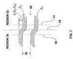
- FIG. 7is a diagram showing a band-gap of the detector device under bias.
- FIG. 8is a diagram of the detector device showing a reduced band-gap under bias and receiving an EM wave.
- an electromagnetic wave having a frequency below the plasma frequency of a metalis reflected. Electrons within the metal shield the electric field of the electromagnetic wave. On the other hand, an electromagnetic wave having a frequency above the plasma frequency is coupled through the metal. Here, the electrons are unable to respond fast enough to shield the metal from the electromagnetic wave.
- Silver (Ag)is a material having a plasma frequency of about 714 terahertz (0.42 microns) or in ultraviolet portion of the electromagnetic spectrum. Thus, silver reflects electromagnetic radiation over the entire visible portion of the spectrum and below.
- Goldhas a plasma frequency in the blue portion of the visible spectrum around 612 terahertz (0.49 microns)
- copper (Cu)has a plasma frequency of about 566 terahertz (0.53 microns) in the green portion of the visible spectrum.
- silver, gold and copperare at least some metals that interact with electromagnetic radiation within the visible portion of the electromagnetic spectrum and below.
- references to plasmonsare not limiting and can include the more general case of charge density waves.
- a junctionsuch as a metallurgical junction or PN junction, is formed between two regions, which have distinct conductivity types. The junction creates an inherent field.
- a plasmon sourceis positioned generally near the junction and receives an electromagnetic wave. The plasmon source generates plasmons having a field. An interaction occurs between the inherent field and the field from the plasmons. This causes the band-gap to diminish and reduces the width of the depletion region. Hence, a current is coupled through the device and indicates energy in the form of plasmons is detected.
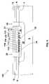
- FIG. 1is an enlarged cross-sectional side-view showing a portion of a semiconductor component 100 near the beginning of fabrication.
- a thin layer of a dielectric materialcan be formed on a major surface 4 of a substrate 2 .
- the dielectric layercommonly referred to as a screen oxide 7
- the screen oxide 7is a sacrificial layer that serves to collect dislodged particles resulting from subsequent processing employing an ion-implantation beam.
- the screen oxide 7typically randomly scatters the beam to reduce channeling.
- a photoresist layer 3for example, can be patterned having an opening 11 which exposes a portion of the screen oxide 7 .
- Ion-implantationcan be used to introduce a dopant into the substrate 2 to form a region 32 .
- the dopantcan include any suitable impurity material such as arsenic, antimony, phosphorus, or the like.
- a dopantcan be introduced using a diffusion method, without a screen oxide.
- Various diffusion techniquescan be used and are well known to those skilled in the art.
- the substrate 2can include compound semiconductors, silicon-on-insulator, silicon-on-sapphire, silicon-on-spinel, silicon-on-nitride, silicon-on-oxide, and the like.
- the type of material for making the substrate 2 and the method of introducing a dopantare not limiting.
- FIG. 2shows a portion of the device 100 after a drive-in oxidation step.
- the dopant comprising region 32is driven deeper into the substrate 2 using various diffusion techniques well known to those in the art. For example, a wet or dry oxidation process step can be used. Similar to the process shown for FIG. 1 , another dopant of an opposite conductivity type is introduced into the substrate 2 to form a region 36 above the region 32 . This dopant can include any suitable impurity material such as boron, or the like.
- the photoresist 3 and screen oxide 7are removed after the implantation steps.
- a final drive-in oxidation stepcan be used to redistribute the dopants of regions 32 and 36 and forms a dielectric layer 8 .
- dielectric layer 8can include using other techniques such as chemical vapor deposition (CVD) and plasma enhanced vapor deposition (PECVD) and is not limiting.
- CVDchemical vapor deposition
- PECVDplasma enhanced vapor deposition
- FIG. 3shows a portion the device 100 after further processing.
- a photoresist(not shown) is patterned and formed on the dielectric layer 8 . Openings 15 are etched through the dielectric layer 8 .
- the plasmon sourcecan include a transmission line, a microstructure, a micro-resonant structure having a cavity, a portion of metallization within a microcircuit, and is not limiting.
- the plasmon source 14can be formed on either side of the junction 34 .
- the plasmon source 14can include resonant, sub-wavelength and wavelength structures and can be sized to a multiple of the wavelength.
- the shape of the plasmon source 14can include spherical, cubical, triangular-pyramidal and the like. In another embodiment (not shown), a plasmon source can extend over a range of distances from a junction and is not limiting.
- a devicesuch as a transistor, can include a plasmon source near a junction and is not limiting as to the type of device. Portions of the region 36 exposed by the openings 15 , shown in FIG. 3 , are etched away using, for example, an anisotropic reactive ion etch. As shown in FIG. 4 , the plasmon source 14 comprises microstructures 17 A- 17 I and is formed above the junction 34 . The microstructures 17 A through 17 I are formed in the etched away portions of the region 36 and fill up to a surface 5 of the dielectric layer 8 using, e.g., techniques described above. The microstructures 17 A- 17 I can be made using materials that include at least gold, silver, copper, aluminum and the like.
- a dielectric layer 9is formed on the microstructures 17 A- 17 I and the dielectric layer 8 .
- the index of refraction of the dielectric layer 9should be greater than the index of refraction of the dielectric layer 8 .
- the preferred thickness of the dielectric layer 9can include a broad range of thicknesses.
- the thickness of the dielectric layer 9can include a range of thicknesses from about 750 Angstroms to about 3,000 Angstroms.
- the material for the dielectric layer 9can include various transparent or translucent materials such as silicon oxide, silicon carbide, and the like.
- the dielectric layer 9can be formed using techniques commonly known in the semiconductor industry. These techniques can include various forms of chemical vapor deposition (CVD) and plasma enhanced vapor deposition (PECVD). The material and technique for making the dielectric layer 9 can take a variety of forms and is not limiting.
- the dielectric layer 9can be planarized using Chemical Mechanical Polishing (CMP).
- CMPChemical Mechanical Polishing
- a dielectric layer 10is formed on the dielectric layer 9 .
- the index of refraction of the dielectric layer 10should be less than the index of refraction of the dielectric layer 9 .
- the thickness of dielectric layer 10can be similar to the thickness of the dielectric layer 9 .
- a dielectric layer 12is formed on the dielectric layer 10 to provide isolation and has an index of refraction less than the dielectric layer 9 .
- a photoresist layer(not shown) is patterned on the dielectric layer 12 to form openings 25 and 29 using techniques well known to those skilled in the art.
- the opening 25 and 29can be formed using an anisotropic reactive ion etch that stops on the surface 4 .
- An opening 27can be similarly formed to stop on the dielectric layer 8 .
- metallization 20 and 22fills the respective openings 25 and 29 (see FIG. 4 ).
- a dielectric material 16is formed in the opening 27 (see FIG. 4 ) using various techniques such as chemical vapor deposition (CVD) and plasma enhanced vapor deposition (PECVD).
- the dielectric material 16should have an index of refraction similar to the index of refraction of the dielectric layer 9 .
- the metallization 20 and 22electrically connects to regions 36 and 32 , respectively.
- the microstructures 17 A- 17 Iare shown in FIG. 5 respectively from left to right.
- the dopant of region 32provides excess carriers (e.g., electrons) that diffuse from the region 32 and combine with carriers (e.g., holes) in the region 36 .
- the dopant from region 36provides excess carriers (e.g., holes) that travel or diffuse and combine with carriers (e.g., electrons) in the region 32 .
- a portion of the regions 32 and 36 within the dashed lines shown near junction 34is commonly referred to as a depletion region 40 .
- a portion of the carriers reaching their respective regions 32 and 36 across the junction 34do not combine.
- uncovered chargeswhich form space charge regions on each side of the junction 34 .
- the uncovered chargesgenerate an inherent field 38 , which is directed from the uncovered charges (e.g., holes) across the junction 34 .
- a potential barrier or built-in voltage V bioccurs across the junction 34 from the inherent field 38 , and for silicon is about 0.6 volt.
- Electrodes 44 and 46are formed on the respective metallization 20 and 22 .
- the electrode 46is shown connected to ground.
- a voltage source(not shown) is connected to the electrode 44 .
- An applied voltage V B from the voltage sourceis generally within a range from about zero volts to a voltage of less than the built-in voltage V bi such that a current does not couple across the junction 34 .
- a coupler 50is for coupling an electromagnetic wave 24 (EM wave) to the microstructures 17 A- 17 I and includes the dielectric material 16 and a portion of the dielectric layers 8 , 9 , 10 and 12 .
- the dielectric layer 9 and the dielectric material 16can serve as the core of the coupler 50 .
- the dielectric layers 8 , 10 and 12function as the coupler's 50 cladding.
- the EM wave 24shown traveling through the dielectric layer 9 of the coupler 50 , can be provided by an external source (not shown) coupled to an end 49 of the coupler 50 .
- a ferrule 48 as showncan be used to connect the external source to the coupler 50 .
- At least a portion of the microstructures 17 A- 17 Iis exposed to the core or the dielectric layer 9 , which carries the EM wave 24 .
- An interaction between the EM wave 24 and the microstructures 17 A- 17 Istimulate plasmons having fields 26 .
- the fields 26can be intensified or concentrated at the corners 18 of the microstructures 17 A- 17 I.
- the EM wave 24can interact with the microstructures 17 A- 17 I over a range of frequencies.
- the fields 26 from the microstructures 17 A- 17 Ican buck or oppose the inherent field 38 across the junction 34 . As a result, the band-gap is reduced, thereby allowing a current 28 to flow across the junction 34 and through the device 100 . Hence, the current 28 is generated on detecting the plasmons.
- Thisprovides an alternative method for detecting plasmons.
- no particular semiconductorcan absorb electromagnetic radiation across the entire visible portion of the electromagnetic spectrum and below.
- silverfor example, interacts with electromagnetic radiation generally across the visible spectrum and below.
- the device 100can be formed using the microstructures 17 A- 17 I made from silver, or a number of other materials that interact with electromagnetic radiation.
- the device 100provides the advantage of using one structure to cover the entire visible spectrum and below.
- semiconductor devices that use absorption to detect electromagnetic radiationcannot continuously function over the visible spectrum and below.
- the response speed of semiconductor detectorsis limited. Carriers within a semiconductor detector that are generated outside the depletion region are delayed, because they must travel to the junction. For this reason and to increase the absorption area, the width of the depletion region is typically increased. However, too wide a depletion region can also result in an increase of the travel-time of the carriers. In contrast, if the depletion region is biased too thin, capacitance will increase causing the response of the semiconductor detector to increase (S. M., Sze, “Semiconductor Devices Physics and Technology”, 2002, page 315).
- FIG. 6is an enlarged top-view of the device 100 shown in FIG. 5 .
- FIG. 6illustrates a microstructure array 31 forming rows 13 , 19 , 21 , 23 and 29 .
- row 21the microstructures 17 A- 17 I are shown respectively from left to right.
- Electrodes 44 and 46 for respectively connecting to a voltage source and to groundare shown.
- FIG. 7is an energy diagram of a band-gap 30 between the top of the valence band EV and the bottom of the conduction band EC shown at an applied voltage of V B . Regions 32 and 36 , junction 34 and the boundaries of the depletion region 40 are overlaid on the energy diagram.
- the applied voltage V Bis shown connected to the electrode 44 in FIG. 5 and has a magnitude between zero and the built-in potential V bi , (i.e., 0 ⁇ V B ⁇ V bi ).
- the applied voltage V Bprovides a potential energy difference (i.e., q (V bi ⁇ V B )) across the junction 34 .
- the energy difference across the junction 34is the charge (q) (e.g., coulombs) multiplied by built-in voltage V bi minus the applied voltage V B (e.g., joule/coulomb).
- V Bbuilt-in voltage
- qcharge
- V biapplied voltage
- V Bapplied voltage
- a voltage of 0.3 voltis applied to the electrode 44 and opposes a built-in voltage V bi of 0.6 resulting in a voltage of about 0.3 volt across the junction 34 .
- the band-gap 30is a function of a number of variables including the net electrostatic potential across the junction 34 .
- the band-gap 30can be increased or decreased by an applied voltage across the device 100 .
- the band-gap 30is reduced by the applied voltage V B , because the field from the applied voltage V B opposes the inherent field 38 of the built-in voltage V bi .
- a carriere.g., electron
- the carrierneeds sufficient energy to reach the lowest energy level of the conduction band E c .
- the carrierneeds to overcome the energy difference (i.e., q (V bi ⁇ V B ) across the junction 34 .
- FIG. 8is an energy diagram of the device 100 illustrating a reduced band-gap 30 on receiving the EM wave 24 .
- the EM wave 24stimulates plasmons that generate the field 26 , which reduces the band-gap 30 .
- the field 26opposes the inherent field 38 , thereby reducing the band-gap 30 .
- the field 26introduces a plasmon voltage V P .
- the corresponding potential energy difference (i.e., q (V bi ⁇ V B ⁇ V P )) across the junction 34is decreased by the plasmon voltage V P .
- Carrierse.g., electrons
- the current 28flows across the junction 34 and through the device 100 .
- Methods of making a device for detecting an electromagnetic wave as can be employed hereinmay use, e.g., the techniques described in related U.S. applications Ser. Nos. 10/917,571 and/or 11/203,407, each of which is described in greater detail above.
- the devices described hereinmay also employ various similar or different example resonant structures like those described in one or more of the following, related applications, each of which was described in greater detail above: U.S. applications Ser. Nos. 11/243,476; 11/243,477; 11/238,991; 11/302,471; 11/325,432; 11/325,448; 11/325,571 and 11/325,534.
- a metallurgical junctionis formed and provides an inherent field across the junction.
- a built-in voltageresults from the inherent field.
- a band-gapis established.
- the metallurgical junctioncan be biased between zero and the built-in voltage.
- a plasmon sourceis formed near the junction.
- An electromagnetic waveis received and channeled to expose the plasmon source, and plasmons are stimulated.
- a fieldoccurs from the stimulated plasmons that oppose the inherent field.
- a net electrostatic potential across the junctionis reduced.
- the band-gapis reduced, and a current is coupled across the junction and through the device on detecting the plasmons.
Landscapes
- Investigating Or Analysing Materials By Optical Means (AREA)
- Photometry And Measurement Of Optical Pulse Characteristics (AREA)
Abstract
Description
- 1. U.S. application Ser. No. 10/917,571, filed on Aug. 13, 2004, entitled “Patterning Thin Metal Film by Dry Reactive Ion Etching”
- 2. U.S. application Ser. No. 11/203,407, filed Aug. 15, 2005, entitled “Method of Patterning Ultra-Small Structures,”
- 3. U.S. application Ser. No. 11/243,476, filed Oct. 5, 2005, entitled, “Structure and Methods for Coupling Energy from an Electromagnetic Wave;”
- 4. U.S. application Ser. No. 11/243,477, filed Oct. 5, 2005, entitled, “Electron Beam Induced Resonance;”
- 5. U.S. application Ser. No. 11/238,991, filed Sep. 30, 2005, entitled, “Light Emitting Free-Electron Micro-Resonant Structure;”
- 6. U.S. application Ser. No. 11/302,471, filed Dec. 14, 2005, entitled, “Coupled Nano-Resonating Energy Emitting Structures;”
- 7. U.S. application Ser. No. 11/325,432, filed Jan. 5, 2006, entitled, “Resonant Structure-Based Display;”
- 8. U.S. application Ser. No. 11/325,448, filed Jan. 5, 2006, entitled, “Selectable Frequency Light Emitter;”
- 9. U.S. application Ser. No. 11/325,571, filed Jan. 5, 2006, entitled, “Switching Micro-Resonant Structures by Modulating a Beam of Charged Particles;” and
- 10. U.S. application Ser. No. 11/325,534, filed Jan. 5, 2006, entitled, “Switching Micro-Resonant Structures Using at Least One Director.”
Claims (10)
Priority Applications (4)
| Application Number | Priority Date | Filing Date | Title |
|---|---|---|---|
| US11/418,084US7586167B2 (en) | 2006-05-05 | 2006-05-05 | Detecting plasmons using a metallurgical junction |
| PCT/US2006/022770WO2008121097A1 (en) | 2006-05-05 | 2006-06-12 | Detecting plasmons using a metallurgical junction |
| EP06852028AEP2022094A4 (en) | 2006-05-05 | 2006-06-12 | DETECTION OF PLASMONS USING A METAL JUNCTION |
| TW095122134ATW200743235A (en) | 2006-05-05 | 2006-06-20 | Detecting plasmons using a metallurgical junction |
Applications Claiming Priority (1)
| Application Number | Priority Date | Filing Date | Title |
|---|---|---|---|
| US11/418,084US7586167B2 (en) | 2006-05-05 | 2006-05-05 | Detecting plasmons using a metallurgical junction |
Publications (2)
| Publication Number | Publication Date |
|---|---|
| US20070257328A1 US20070257328A1 (en) | 2007-11-08 |
| US7586167B2true US7586167B2 (en) | 2009-09-08 |
Family
ID=38660439
Family Applications (1)
| Application Number | Title | Priority Date | Filing Date |
|---|---|---|---|
| US11/418,084ActiveUS7586167B2 (en) | 2006-05-05 | 2006-05-05 | Detecting plasmons using a metallurgical junction |
Country Status (4)
| Country | Link |
|---|---|
| US (1) | US7586167B2 (en) |
| EP (1) | EP2022094A4 (en) |
| TW (1) | TW200743235A (en) |
| WO (1) | WO2008121097A1 (en) |
Cited By (22)
| Publication number | Priority date | Publication date | Assignee | Title |
|---|---|---|---|---|
| US20070257208A1 (en)* | 2006-05-05 | 2007-11-08 | Virgin Islands Microsystems, Inc. | Electron accelerator for ultra-small resonant structures |
| US20080099793A1 (en)* | 2006-10-13 | 2008-05-01 | David Fattal | Photodiode module and apparatus including multiple photodiode modules |
| US20090230332A1 (en)* | 2007-10-10 | 2009-09-17 | Virgin Islands Microsystems, Inc. | Depressed Anode With Plasmon-Enabled Devices Such As Ultra-Small Resonant Structures |
| US7655934B2 (en) | 2006-06-28 | 2010-02-02 | Virgin Island Microsystems, Inc. | Data on light bulb |
| US7679067B2 (en) | 2006-05-26 | 2010-03-16 | Virgin Island Microsystems, Inc. | Receiver array using shared electron beam |
| US7688274B2 (en) | 2006-02-28 | 2010-03-30 | Virgin Islands Microsystems, Inc. | Integrated filter in antenna-based detector |
| US7710040B2 (en) | 2006-05-05 | 2010-05-04 | Virgin Islands Microsystems, Inc. | Single layer construction for ultra small devices |
| US7714513B2 (en) | 2005-09-30 | 2010-05-11 | Virgin Islands Microsystems, Inc. | Electron beam induced resonance |
| US7718977B2 (en) | 2006-05-05 | 2010-05-18 | Virgin Island Microsystems, Inc. | Stray charged particle removal device |
| US7728397B2 (en) | 2006-05-05 | 2010-06-01 | Virgin Islands Microsystems, Inc. | Coupled nano-resonating energy emitting structures |
| US7728702B2 (en) | 2006-05-05 | 2010-06-01 | Virgin Islands Microsystems, Inc. | Shielding of integrated circuit package with high-permeability magnetic material |
| US7732786B2 (en) | 2006-05-05 | 2010-06-08 | Virgin Islands Microsystems, Inc. | Coupling energy in a plasmon wave to an electron beam |
| US7741934B2 (en) | 2006-05-05 | 2010-06-22 | Virgin Islands Microsystems, Inc. | Coupling a signal through a window |
| US7746532B2 (en) | 2006-05-05 | 2010-06-29 | Virgin Island Microsystems, Inc. | Electro-optical switching system and method |
| US7791291B2 (en) | 2005-09-30 | 2010-09-07 | Virgin Islands Microsystems, Inc. | Diamond field emission tip and a method of formation |
| US7876793B2 (en) | 2006-04-26 | 2011-01-25 | Virgin Islands Microsystems, Inc. | Micro free electron laser (FEL) |
| US20110155891A1 (en)* | 2009-12-28 | 2011-06-30 | Sony Corporation | Semiconductor device and electronic apparatus |
| US7986113B2 (en) | 2006-05-05 | 2011-07-26 | Virgin Islands Microsystems, Inc. | Selectable frequency light emitter |
| US7990336B2 (en) | 2007-06-19 | 2011-08-02 | Virgin Islands Microsystems, Inc. | Microwave coupled excitation of solid state resonant arrays |
| US20110215231A1 (en)* | 2003-10-31 | 2011-09-08 | Fattal David A | Photodiode module and apparatus including multiple photodiode modules |
| US8188431B2 (en) | 2006-05-05 | 2012-05-29 | Jonathan Gorrell | Integration of vacuum microelectronic device with integrated circuit |
| US8384042B2 (en) | 2006-01-05 | 2013-02-26 | Advanced Plasmonics, Inc. | Switching micro-resonant structures by modulating a beam of charged particles |
Families Citing this family (7)
| Publication number | Priority date | Publication date | Assignee | Title |
|---|---|---|---|---|
| JP5715154B2 (en) | 2009-12-14 | 2015-05-07 | ユニバーシティ オブ メリーランド,ボルチモア カウンティ | Plasmon Electric |
| US20110215705A1 (en)* | 2010-03-05 | 2011-09-08 | James Peter Long | Micro-chip plasmonic source |
| US8735175B2 (en) | 2011-03-18 | 2014-05-27 | Chris D. Geddes | Multicolor microwave-accelerated metal-enhanced fluorescence (M-MAMEF) |
| TW201430899A (en)* | 2013-01-31 | 2014-08-01 | Oriental System Technology Inc | Non-dispersive infrared gas detector, and method of stabilizing infrared emission of an incandescent lamp in the same |
| FR3051557A1 (en)* | 2016-05-17 | 2017-11-24 | Univ Aix Marseille | PARTICULATE DETECTOR PRODUCED IN SEMICONDUCTOR MATERIAL |
| US11428690B2 (en)* | 2017-01-30 | 2022-08-30 | University Of Miami | Portable plasmonic system for disease detection |
| JP7034016B2 (en)* | 2018-06-25 | 2022-03-11 | 浜松ホトニクス株式会社 | Photodetector |
Citations (279)
| Publication number | Priority date | Publication date | Assignee | Title |
|---|---|---|---|---|
| US1948384A (en) | 1932-01-26 | 1934-02-20 | Research Corp | Method and apparatus for the acceleration of ions |
| US2307086A (en) | 1941-05-07 | 1943-01-05 | Univ Leland Stanford Junior | High frequency electrical apparatus |
| US2431396A (en) | 1942-12-21 | 1947-11-25 | Rca Corp | Current magnitude-ratio responsive amplifier |
| US2473477A (en) | 1946-07-24 | 1949-06-14 | Raythcon Mfg Company | Magnetic induction device |
| US2634372A (en) | 1953-04-07 | Super high-frequency electromag | ||
| US2932798A (en) | 1956-01-05 | 1960-04-12 | Research Corp | Imparting energy to charged particles |
| US2944183A (en) | 1957-01-25 | 1960-07-05 | Bell Telephone Labor Inc | Internal cavity reflex klystron tuned by a tightly coupled external cavity |
| US2966611A (en) | 1959-07-21 | 1960-12-27 | Sperry Rand Corp | Ruggedized klystron tuner |
| US3231779A (en) | 1962-06-25 | 1966-01-25 | Gen Electric | Elastic wave responsive apparatus |
| US3297905A (en) | 1963-02-06 | 1967-01-10 | Varian Associates | Electron discharge device of particular materials for stabilizing frequency and reducing magnetic field problems |
| US3315117A (en) | 1963-07-15 | 1967-04-18 | Burton J Udelson | Electrostatically focused electron beam phase shifter |
| US3387169A (en) | 1965-05-07 | 1968-06-04 | Sfd Lab Inc | Slow wave structure of the comb type having strap means connecting the teeth to form iterative inductive shunt loadings |
| US3543147A (en) | 1968-03-29 | 1970-11-24 | Atomic Energy Commission | Phase angle measurement system for determining and controlling the resonance of the radio frequency accelerating cavities for high energy charged particle accelerators |
| US3546524A (en) | 1967-11-24 | 1970-12-08 | Varian Associates | Linear accelerator having the beam injected at a position of maximum r.f. accelerating field |
| US3560694A (en) | 1969-01-21 | 1971-02-02 | Varian Associates | Microwave applicator employing flat multimode cavity for treating webs |
| US3571642A (en) | 1968-01-17 | 1971-03-23 | Ca Atomic Energy Ltd | Method and apparatus for interleaved charged particle acceleration |
| US3586899A (en) | 1968-06-12 | 1971-06-22 | Ibm | Apparatus using smith-purcell effect for frequency modulation and beam deflection |
| US3761828A (en) | 1970-12-10 | 1973-09-25 | J Pollard | Linear particle accelerator with coast through shield |
| US3886399A (en) | 1973-08-20 | 1975-05-27 | Varian Associates | Electron beam electrical power transmission system |
| US3923568A (en) | 1974-01-14 | 1975-12-02 | Int Plasma Corp | Dry plasma process for etching noble metal |
| US3989347A (en) | 1974-06-20 | 1976-11-02 | Siemens Aktiengesellschaft | Acousto-optical data input transducer with optical data storage and process for operation thereof |
| US4053845A (en) | 1967-03-06 | 1977-10-11 | Gordon Gould | Optically pumped laser amplifiers |
| US4282436A (en) | 1980-06-04 | 1981-08-04 | The United States Of America As Represented By The Secretary Of The Navy | Intense ion beam generation with an inverse reflex tetrode (IRT) |
| US4450554A (en) | 1981-08-10 | 1984-05-22 | International Telephone And Telegraph Corporation | Asynchronous integrated voice and data communication system |
| US4482779A (en)* | 1983-04-19 | 1984-11-13 | The United States Of America As Represented By The Administrator Of National Aeronautics And Space Administration | Inelastic tunnel diodes |
| US4528659A (en) | 1981-12-17 | 1985-07-09 | International Business Machines Corporation | Interleaved digital data and voice communications system apparatus and method |
| US4589107A (en) | 1982-11-30 | 1986-05-13 | Itt Corporation | Simultaneous voice and data communication and data base access in a switching system using a combined voice conference and data base processing module |
| US4598397A (en) | 1984-02-21 | 1986-07-01 | Cxc Corporation | Microtelephone controller |
| US4630262A (en) | 1984-05-23 | 1986-12-16 | International Business Machines Corp. | Method and system for transmitting digitized voice signals as packets of bits |
| US4652703A (en) | 1983-03-01 | 1987-03-24 | Racal Data Communications Inc. | Digital voice transmission having improved echo suppression |
| WO1987001873A1 (en) | 1985-09-19 | 1987-03-26 | Hughes Aircraft Company | Radiation source |
| US4661783A (en) | 1981-03-18 | 1987-04-28 | The United States Of America As Represented By The Secretary Of The Navy | Free electron and cyclotron resonance distributed feedback lasers and masers |
| US4704583A (en) | 1974-08-16 | 1987-11-03 | Gordon Gould | Light amplifiers employing collisions to produce a population inversion |
| US4712042A (en) | 1986-02-03 | 1987-12-08 | Accsys Technology, Inc. | Variable frequency RFQ linear accelerator |
| US4713581A (en) | 1983-08-09 | 1987-12-15 | Haimson Research Corporation | Method and apparatus for accelerating a particle beam |
| US4740963A (en) | 1986-01-30 | 1988-04-26 | Lear Siegler, Inc. | Voice and data communication system |
| US4740973A (en) | 1984-05-21 | 1988-04-26 | Madey John M J | Free electron laser |
| US4746201A (en) | 1967-03-06 | 1988-05-24 | Gordon Gould | Polarizing apparatus employing an optical element inclined at brewster's angle |
| US4761059A (en) | 1986-07-28 | 1988-08-02 | Rockwell International Corporation | External beam combining of multiple lasers |
| US4782485A (en) | 1985-08-23 | 1988-11-01 | Republic Telcom Systems Corporation | Multiplexed digital packet telephone system |
| US4789945A (en) | 1985-07-29 | 1988-12-06 | Advantest Corporation | Method and apparatus for charged particle beam exposure |
| US4806859A (en) | 1987-01-27 | 1989-02-21 | Ford Motor Company | Resonant vibrating structures with driving sensing means for noncontacting position and pick up sensing |
| US4809271A (en) | 1986-11-14 | 1989-02-28 | Hitachi, Ltd. | Voice and data multiplexer system |
| US4813040A (en) | 1986-10-31 | 1989-03-14 | Futato Steven P | Method and apparatus for transmitting digital data and real-time digitalized voice information over a communications channel |
| US4819228A (en) | 1984-10-29 | 1989-04-04 | Stratacom Inc. | Synchronous packet voice/data communication system |
| US4829527A (en) | 1984-04-23 | 1989-05-09 | The United States Of America As Represented By The Secretary Of The Army | Wideband electronic frequency tuning for orotrons |
| US4838021A (en) | 1987-12-11 | 1989-06-13 | Hughes Aircraft Company | Electrostatic ion thruster with improved thrust modulation |
| US4841538A (en) | 1986-03-05 | 1989-06-20 | Kabushiki Kaisha Toshiba | CO2 gas laser device |
| US4864131A (en) | 1987-11-09 | 1989-09-05 | The University Of Michigan | Positron microscopy |
| US4866704A (en) | 1988-03-16 | 1989-09-12 | California Institute Of Technology | Fiber optic voice/data network |
| US4866732A (en) | 1985-02-04 | 1989-09-12 | Mitel Telecom Limited | Wireless telephone system |
| US4873715A (en) | 1986-06-10 | 1989-10-10 | Hitachi, Ltd. | Automatic data/voice sending/receiving mode switching device |
| US4887265A (en) | 1988-03-18 | 1989-12-12 | Motorola, Inc. | Packet-switched cellular telephone system |
| US4890282A (en) | 1988-03-08 | 1989-12-26 | Network Equipment Technologies, Inc. | Mixed mode compression for data transmission |
| US4898022A (en) | 1987-02-09 | 1990-02-06 | Tlv Co., Ltd. | Steam trap operation detector |
| US4912705A (en) | 1985-03-20 | 1990-03-27 | International Mobile Machines Corporation | Subscriber RF telephone system for providing multiple speech and/or data signals simultaneously over either a single or a plurality of RF channels |
| US4932022A (en) | 1987-10-07 | 1990-06-05 | Telenova, Inc. | Integrated voice and data telephone system |
| US4981371A (en) | 1989-02-17 | 1991-01-01 | Itt Corporation | Integrated I/O interface for communication terminal |
| US5023563A (en) | 1989-06-08 | 1991-06-11 | Hughes Aircraft Company | Upshifted free electron laser amplifier |
| US5036513A (en) | 1989-06-21 | 1991-07-30 | Academy Of Applied Science | Method of and apparatus for integrated voice (audio) communication simultaneously with "under voice" user-transparent digital data between telephone instruments |
| US5065425A (en) | 1988-12-23 | 1991-11-12 | Telic Alcatel | Telephone connection arrangement for a personal computer and a device for such an arrangement |
| US5113141A (en) | 1990-07-18 | 1992-05-12 | Science Applications International Corporation | Four-fingers RFQ linac structure |
| US5121385A (en) | 1988-09-14 | 1992-06-09 | Fujitsu Limited | Highly efficient multiplexing system |
| US5127001A (en) | 1990-06-22 | 1992-06-30 | Unisys Corporation | Conference call arrangement for distributed network |
| US5128729A (en) | 1990-11-13 | 1992-07-07 | Motorola, Inc. | Complex opto-isolator with improved stand-off voltage stability |
| US5130985A (en) | 1988-11-25 | 1992-07-14 | Hitachi, Ltd. | Speech packet communication system and method |
| US5150410A (en) | 1991-04-11 | 1992-09-22 | Itt Corporation | Secure digital conferencing system |
| US5155726A (en) | 1990-01-22 | 1992-10-13 | Digital Equipment Corporation | Station-to-station full duplex communication in a token ring local area network |
| US5157000A (en) | 1989-07-10 | 1992-10-20 | Texas Instruments Incorporated | Method for dry etching openings in integrated circuit layers |
| US5163118A (en) | 1986-11-10 | 1992-11-10 | The United States Of America As Represented By The Secretary Of The Air Force | Lattice mismatched hetrostructure optical waveguide |
| US5185073A (en) | 1988-06-21 | 1993-02-09 | International Business Machines Corporation | Method of fabricating nendritic materials |
| US5187591A (en) | 1991-01-24 | 1993-02-16 | Micom Communications Corp. | System for transmitting and receiving aural information and modulated data |
| US5199918A (en) | 1991-11-07 | 1993-04-06 | Microelectronics And Computer Technology Corporation | Method of forming field emitter device with diamond emission tips |
| US5214650A (en) | 1990-11-19 | 1993-05-25 | Ag Communication Systems Corporation | Simultaneous voice and data system using the existing two-wire inter-face |
| US5233623A (en) | 1992-04-29 | 1993-08-03 | Research Foundation Of State University Of New York | Integrated semiconductor laser with electronic directivity and focusing control |
| US5235248A (en) | 1990-06-08 | 1993-08-10 | The United States Of America As Represented By The United States Department Of Energy | Method and split cavity oscillator/modulator to generate pulsed particle beams and electromagnetic fields |
| WO1993021663A1 (en) | 1992-04-08 | 1993-10-28 | Georgia Tech Research Corporation | Process for lift-off of thin film materials from a growth substrate |
| US5263043A (en) | 1990-08-31 | 1993-11-16 | Trustees Of Dartmouth College | Free electron laser utilizing grating coupling |
| US5262656A (en) | 1991-06-07 | 1993-11-16 | Thomson-Csf | Optical semiconductor transceiver with chemically resistant layers |
| US5268788A (en) | 1991-06-25 | 1993-12-07 | Smiths Industries Public Limited Company | Display filter arrangements |
| US5268693A (en) | 1990-08-31 | 1993-12-07 | Trustees Of Dartmouth College | Semiconductor film free electron laser |
| US5282197A (en) | 1992-05-15 | 1994-01-25 | International Business Machines | Low frequency audio sub-channel embedded signalling |
| US5283819A (en) | 1991-04-25 | 1994-02-01 | Compuadd Corporation | Computing and multimedia entertainment system |
| US5293175A (en) | 1991-07-19 | 1994-03-08 | Conifer Corporation | Stacked dual dipole MMDS feed |
| US5302240A (en) | 1991-01-22 | 1994-04-12 | Kabushiki Kaisha Toshiba | Method of manufacturing semiconductor device |
| US5305312A (en) | 1992-02-07 | 1994-04-19 | At&T Bell Laboratories | Apparatus for interfacing analog telephones and digital data terminals to an ISDN line |
| US5341374A (en) | 1991-03-01 | 1994-08-23 | Trilan Systems Corporation | Communication network integrating voice data and video with distributed call processing |
| US5446814A (en) | 1993-11-05 | 1995-08-29 | Motorola | Molded reflective optical waveguide |
| US5504341A (en) | 1995-02-17 | 1996-04-02 | Zimec Consulting, Inc. | Producing RF electric fields suitable for accelerating atomic and molecular ions in an ion implantation system |
| US5578909A (en) | 1994-07-15 | 1996-11-26 | The Regents Of The Univ. Of California | Coupled-cavity drift-tube linac |
| US5604352A (en) | 1995-04-25 | 1997-02-18 | Raychem Corporation | Apparatus comprising voltage multiplication components |
| US5608263A (en) | 1994-09-06 | 1997-03-04 | The Regents Of The University Of Michigan | Micromachined self packaged circuits for high-frequency applications |
| US5663971A (en) | 1996-04-02 | 1997-09-02 | The Regents Of The University Of California, Office Of Technology Transfer | Axial interaction free-electron laser |
| US5666020A (en) | 1994-11-16 | 1997-09-09 | Nec Corporation | Field emission electron gun and method for fabricating the same |
| US5668368A (en) | 1992-02-21 | 1997-09-16 | Hitachi, Ltd. | Apparatus for suppressing electrification of sample in charged beam irradiation apparatus |
| US5705443A (en) | 1995-05-30 | 1998-01-06 | Advanced Technology Materials, Inc. | Etching method for refractory materials |
| US5737458A (en) | 1993-03-29 | 1998-04-07 | Martin Marietta Corporation | Optical light pipe and microwave waveguide interconnects in multichip modules formed using adaptive lithography |
| US5744919A (en) | 1996-12-12 | 1998-04-28 | Mishin; Andrey V. | CW particle accelerator with low particle injection velocity |
| US5757009A (en) | 1996-12-27 | 1998-05-26 | Northrop Grumman Corporation | Charged particle beam expander |
| US5767013A (en) | 1996-08-26 | 1998-06-16 | Lg Semicon Co., Ltd. | Method for forming interconnection in semiconductor pattern device |
| US5780970A (en) | 1996-10-28 | 1998-07-14 | University Of Maryland | Multi-stage depressed collector for small orbit gyrotrons |
| US5790585A (en) | 1996-11-12 | 1998-08-04 | The Trustees Of Dartmouth College | Grating coupling free electron laser apparatus and method |
| US5811943A (en) | 1996-09-23 | 1998-09-22 | Schonberg Research Corporation | Hollow-beam microwave linear accelerator |
| US5821836A (en) | 1997-05-23 | 1998-10-13 | The Regents Of The University Of Michigan | Miniaturized filter assembly |
| US5821902A (en) | 1993-09-02 | 1998-10-13 | Inmarsat | Folded dipole microstrip antenna |
| US5825140A (en) | 1996-02-29 | 1998-10-20 | Nissin Electric Co., Ltd. | Radio-frequency type charged particle accelerator |
| US5831270A (en) | 1996-02-19 | 1998-11-03 | Nikon Corporation | Magnetic deflectors and charged-particle-beam lithography systems incorporating same |
| US5847745A (en) | 1995-03-03 | 1998-12-08 | Futaba Denshi Kogyo K.K. | Optical write element |
| US5889449A (en) | 1995-12-07 | 1999-03-30 | Space Systems/Loral, Inc. | Electromagnetic transmission line elements having a boundary between materials of high and low dielectric constants |
| US5889797A (en) | 1996-08-26 | 1999-03-30 | The Regents Of The University Of California | Measuring short electron bunch lengths using coherent smith-purcell radiation |
| US5902489A (en) | 1995-11-08 | 1999-05-11 | Hitachi, Ltd. | Particle handling method by acoustic radiation force and apparatus therefore |
| US5963857A (en) | 1998-01-20 | 1999-10-05 | Lucent Technologies, Inc. | Article comprising a micro-machined filter |
| US6005347A (en) | 1995-12-12 | 1999-12-21 | Lg Electronics Inc. | Cathode for a magnetron having primary and secondary electron emitters |
| US6008496A (en) | 1997-05-05 | 1999-12-28 | University Of Florida | High resolution resonance ionization imaging detector and method |
| US6040625A (en) | 1997-09-25 | 2000-03-21 | I/O Sensors, Inc. | Sensor package arrangement |
| US6060833A (en) | 1996-10-18 | 2000-05-09 | Velazco; Jose E. | Continuous rotating-wave electron beam accelerator |
| US6080529A (en) | 1997-12-12 | 2000-06-27 | Applied Materials, Inc. | Method of etching patterned layers useful as masking during subsequent etching or for damascene structures |
| US6139760A (en) | 1997-12-19 | 2000-10-31 | Electronics And Telecommunications Research Institute | Short-wavelength optoelectronic device including field emission device and its fabricating method |
| WO2000072413A2 (en) | 1999-05-25 | 2000-11-30 | Deutsche Telekom Ag | Miniaturized terahertz radiation source |
| US6180415B1 (en) | 1997-02-20 | 2001-01-30 | The Regents Of The University Of California | Plasmon resonant particles, methods and apparatus |
| US6195199B1 (en) | 1997-10-27 | 2001-02-27 | Kanazawa University | Electron tube type unidirectional optical amplifier |
| US6222866B1 (en) | 1997-01-06 | 2001-04-24 | Fuji Xerox Co., Ltd. | Surface emitting semiconductor laser, its producing method and surface emitting semiconductor laser array |
| US6278239B1 (en) | 1996-06-25 | 2001-08-21 | The United States Of America As Represented By The United States Department Of Energy | Vacuum-surface flashover switch with cantilever conductors |
| US6297511B1 (en) | 1999-04-01 | 2001-10-02 | Raytheon Company | High frequency infrared emitter |
| US20010025925A1 (en) | 2000-03-28 | 2001-10-04 | Kabushiki Kaisha Toshiba | Charged particle beam system and pattern slant observing method |
| US6301041B1 (en) | 1998-08-18 | 2001-10-09 | Kanazawa University | Unidirectional optical amplifier |
| US6316876B1 (en) | 1998-08-19 | 2001-11-13 | Eiji Tanabe | High gradient, compact, standing wave linear accelerator structure |
| US6338968B1 (en) | 1998-02-02 | 2002-01-15 | Signature Bioscience, Inc. | Method and apparatus for detecting molecular binding events |
| US20020036121A1 (en) | 2000-09-08 | 2002-03-28 | Ronald Ball | Illumination system for escalator handrails |
| US20020036264A1 (en) | 2000-07-27 | 2002-03-28 | Mamoru Nakasuji | Sheet beam-type inspection apparatus |
| US6370306B1 (en) | 1997-12-15 | 2002-04-09 | Seiko Instruments Inc. | Optical waveguide probe and its manufacturing method |
| US6373194B1 (en) | 2000-06-01 | 2002-04-16 | Raytheon Company | Optical magnetron for high efficiency production of optical radiation |
| US20020053638A1 (en) | 1998-07-03 | 2002-05-09 | Dieter Winkler | Apparatus and method for examing specimen with a charged particle beam |
| US20020068018A1 (en) | 2000-12-06 | 2002-06-06 | Hrl Laboratories, Llc | Compact sensor using microcavity structures |
| US20020071457A1 (en) | 2000-12-08 | 2002-06-13 | Hogan Josh N. | Pulsed non-linear resonant cavity |
| US6407516B1 (en) | 2000-05-26 | 2002-06-18 | Exaconnect Inc. | Free space electron switch |
| WO2002025785A8 (en) | 2000-09-22 | 2002-07-04 | Vermont Photonics | Apparatuses and methods for generating coherent electromagnetic laser radiation |
| US6441298B1 (en)* | 2000-08-15 | 2002-08-27 | Nec Research Institute, Inc | Surface-plasmon enhanced photovoltaic device |
| US6448850B1 (en) | 1999-05-20 | 2002-09-10 | Kanazawa University | Electromagnetic wave amplifier and electromagnetic wave generator |
| US6453087B2 (en) | 2000-04-28 | 2002-09-17 | Confluent Photonics Co. | Miniature monolithic optical add-drop multiplexer |
| US20020135665A1 (en) | 2001-03-20 | 2002-09-26 | Keith Gardner | Led print head for electrophotographic printer |
| US6470198B1 (en) | 1999-04-28 | 2002-10-22 | Murata Manufacturing Co., Ltd. | Electronic part, dielectric resonator, dielectric filter, duplexer, and communication device comprised of high TC superconductor |
| WO2002077607A9 (en) | 2001-03-23 | 2002-11-14 | Vermont Photonics | Applying far infrared radiation to biological matter |
| US20020191650A1 (en) | 2001-02-26 | 2002-12-19 | Madey John M. J. | Phase displacement free-electron laser |
| US20030012925A1 (en) | 2001-07-16 | 2003-01-16 | Motorola, Inc. | Process for fabricating semiconductor structures and devices utilizing the formation of a compliant substrate for materials used to form the same and including an etch stop layer used for back side processing |
| US20030010979A1 (en) | 2000-01-14 | 2003-01-16 | Fabrice Pardo | Vertical metal-semiconductor microresonator photodetecting device and production method thereof |
| US20030016421A1 (en) | 2000-06-01 | 2003-01-23 | Small James G. | Wireless communication system with high efficiency/high power optical source |
| US20030016412A1 (en) | 2001-07-17 | 2003-01-23 | Alcatel | Monitoring unit for optical burst mode signals |
| US20030034535A1 (en) | 2001-08-15 | 2003-02-20 | Motorola, Inc. | Mems devices suitable for integration with chip having integrated silicon and compound semiconductor devices, and methods for fabricating such devices |
| US6525477B2 (en) | 2001-05-29 | 2003-02-25 | Raytheon Company | Optical magnetron generator |
| US6545425B2 (en) | 2000-05-26 | 2003-04-08 | Exaconnect Corp. | Use of a free space electron switch in a telecommunications network |
| US6552320B1 (en)* | 1999-06-21 | 2003-04-22 | United Microelectronics Corp. | Image sensor structure |
| US20030103150A1 (en)* | 2001-11-30 | 2003-06-05 | Catrysse Peter B. | Integrated color pixel ( ICP ) |
| US6577040B2 (en) | 1999-01-14 | 2003-06-10 | The Regents Of The University Of Michigan | Method and apparatus for generating a signal having at least one desired output frequency utilizing a bank of vibrating micromechanical devices |
| US20030106998A1 (en) | 1996-08-08 | 2003-06-12 | William Marsh Rice University | Method for producing boron nitride coatings and fibers and compositions thereof |
| US6580075B2 (en) | 1998-09-18 | 2003-06-17 | Hitachi, Ltd. | Charged particle beam scanning type automatic inspecting apparatus |
| US6603781B1 (en) | 2001-01-19 | 2003-08-05 | Siros Technologies, Inc. | Multi-wavelength transmitter |
| US6603915B2 (en) | 2001-02-05 | 2003-08-05 | Fujitsu Limited | Interposer and method for producing a light-guiding structure |
| US20030158474A1 (en) | 2002-01-18 | 2003-08-21 | Axel Scherer | Method and apparatus for nanomagnetic manipulation and sensing |
| US20030155521A1 (en) | 2000-02-01 | 2003-08-21 | Hans-Peter Feuerbaum | Optical column for charged particle beam device |
| US20030164947A1 (en) | 2000-04-18 | 2003-09-04 | Matthias Vaupel | Spr sensor |
| US6624916B1 (en) | 1997-02-11 | 2003-09-23 | Quantumbeam Limited | Signalling system |
| US20030179974A1 (en) | 2002-03-20 | 2003-09-25 | Estes Michael J. | Surface plasmon devices |
| US6636653B2 (en) | 2001-02-02 | 2003-10-21 | Teravicta Technologies, Inc. | Integrated optical micro-electromechanical systems and methods of fabricating and operating the same |
| US6636185B1 (en) | 1992-03-13 | 2003-10-21 | Kopin Corporation | Head-mounted display system |
| US6640023B2 (en) | 2001-09-27 | 2003-10-28 | Memx, Inc. | Single chip optical cross connect |
| US6642907B2 (en) | 2001-01-12 | 2003-11-04 | The Furukawa Electric Co., Ltd. | Antenna device |
| US20030206708A1 (en) | 2002-03-20 | 2003-11-06 | Estes Michael J. | Surface plasmon devices |
| US20030214695A1 (en) | 2002-03-18 | 2003-11-20 | E Ink Corporation | Electro-optic displays, and methods for driving same |
| JP2004032323A (en) | 2002-06-25 | 2004-01-29 | Toyo Commun Equip Co Ltd | Surface mounting type piezoelectric oscillator and its manufacturing method |
| US6687034B2 (en) | 2001-03-23 | 2004-02-03 | Microvision, Inc. | Active tuning of a torsional resonant structure |
| US20040061053A1 (en) | 2001-02-28 | 2004-04-01 | Yoshifumi Taniguchi | Method and apparatus for measuring physical properties of micro region |
| US6724486B1 (en) | 1999-04-28 | 2004-04-20 | Zygo Corporation | Helium- Neon laser light source generating two harmonically related, single- frequency wavelengths for use in displacement and dispersion measuring interferometry |
| US20040080285A1 (en) | 2000-05-26 | 2004-04-29 | Victor Michel N. | Use of a free space electron switch in a telecommunications network |
| US20040085159A1 (en) | 2002-11-01 | 2004-05-06 | Kubena Randall L. | Micro electrical mechanical system (MEMS) tuning using focused ion beams |
| US20040092104A1 (en) | 2002-06-19 | 2004-05-13 | Luxtera, Inc. | Methods of incorporating germanium within CMOS process |
| US6738176B2 (en) | 2002-04-30 | 2004-05-18 | Mario Rabinowitz | Dynamic multi-wavelength switching ensemble |
| US6741781B2 (en) | 2000-09-29 | 2004-05-25 | Kabushiki Kaisha Toshiba | Optical interconnection circuit board and manufacturing method thereof |
| US20040108471A1 (en) | 2002-09-26 | 2004-06-10 | Chiyan Luo | Photonic crystals: a medium exhibiting anomalous cherenkov radiation |
| US20040108473A1 (en) | 2000-06-09 | 2004-06-10 | Melnychuk Stephan T. | Extreme ultraviolet light source |
| US20040136715A1 (en) | 2002-12-06 | 2004-07-15 | Seiko Epson Corporation | Wavelength multiplexing on-chip optical interconnection circuit, electro-optical device, and electronic apparatus |
| US20040150991A1 (en) | 2003-01-27 | 2004-08-05 | 3M Innovative Properties Company | Phosphor based light sources utilizing total internal reflection |
| US6782205B2 (en) | 2001-06-25 | 2004-08-24 | Silicon Light Machines | Method and apparatus for dynamic equalization in wavelength division multiplexing |
| US20040171272A1 (en) | 2003-02-28 | 2004-09-02 | Applied Materials, Inc. | Method of etching metallic materials to form a tapered profile |
| US6791438B2 (en) | 2001-10-30 | 2004-09-14 | Matsushita Electric Industrial Co., Ltd. | Radio frequency module and method for manufacturing the same |
| US20040180244A1 (en) | 2003-01-24 | 2004-09-16 | Tour James Mitchell | Process and apparatus for microwave desorption of elements or species from carbon nanotubes |
| US20040184270A1 (en) | 2003-03-17 | 2004-09-23 | Halter Michael A. | LED light module with micro-reflector cavities |
| US6800877B2 (en) | 2000-05-26 | 2004-10-05 | Exaconnect Corp. | Semi-conductor interconnect using free space electron switch |
| US20040213375A1 (en) | 2003-04-25 | 2004-10-28 | Paul Bjorkholm | Radiation sources and radiation scanning systems with improved uniformity of radiation intensity |
| US20040218651A1 (en) | 2000-03-03 | 2004-11-04 | Canon Kabushiki Kaisha | Electron-beam excitation laser |
| US20040217297A1 (en) | 2000-12-01 | 2004-11-04 | Yeda Research And Development Co. Ltd. | Device and method for the examination of samples in a non vacuum environment using a scanning electron microscope |
| US6819432B2 (en) | 2001-03-14 | 2004-11-16 | Hrl Laboratories, Llc | Coherent detecting receiver using a time delay interferometer and adaptive beam combiner |
| US20040231996A1 (en) | 2003-05-20 | 2004-11-25 | Novellus Systems, Inc. | Electroplating using DC current interruption and variable rotation rate |
| US20040240035A1 (en) | 2003-05-29 | 2004-12-02 | Stanislav Zhilkov | Method of modulation and electron modulator for optical communication and data transmission |
| US6829286B1 (en) | 2000-05-26 | 2004-12-07 | Opticomp Corporation | Resonant cavity enhanced VCSEL/waveguide grating coupler |
| US6834152B2 (en) | 2001-09-10 | 2004-12-21 | California Institute Of Technology | Strip loaded waveguide with low-index transition layer |
| US20040264867A1 (en) | 2002-12-06 | 2004-12-30 | Seiko Epson Corporation | Optical interconnection circuit among wavelength multiplexing chips, electro-optical device, and electronic apparatus |
| US20050023145A1 (en) | 2003-05-07 | 2005-02-03 | Microfabrica Inc. | Methods and apparatus for forming multi-layer structures using adhered masks |
| WO2005015143A2 (en) | 2003-08-11 | 2005-02-17 | Opgal Ltd. | Radiometry using an uncooled microbolometer detector |
| US20050045821A1 (en) | 2003-04-22 | 2005-03-03 | Nobuharu Noji | Testing apparatus using charged particles and device manufacturing method using the testing apparatus |
| US20050045832A1 (en) | 2003-07-11 | 2005-03-03 | Kelly Michael A. | Non-dispersive charged particle energy analyzer |
| US20050054151A1 (en) | 2002-01-04 | 2005-03-10 | Intersil Americas Inc. | Symmetric inducting device for an integrated circuit having a ground shield |
| US6871025B2 (en) | 2000-06-15 | 2005-03-22 | California Institute Of Technology | Direct electrical-to-optical conversion and light modulation in micro whispering-gallery-mode resonators |
| US6870438B1 (en) | 1999-11-10 | 2005-03-22 | Kyocera Corporation | Multi-layered wiring board for slot coupling a transmission line to a waveguide |
| US20050067286A1 (en) | 2003-09-26 | 2005-03-31 | The University Of Cincinnati | Microfabricated structures and processes for manufacturing same |
| US20050082469A1 (en) | 1997-06-19 | 2005-04-21 | European Organization For Nuclear Research | Neutron-driven element transmuter |
| US6885262B2 (en) | 2002-11-05 | 2005-04-26 | Ube Industries, Ltd. | Band-pass filter using film bulk acoustic resonator |
| US20050092929A1 (en) | 2003-07-08 | 2005-05-05 | Schneiker Conrad W. | Integrated sub-nanometer-scale electron beam systems |
| US20050104684A1 (en) | 2003-10-03 | 2005-05-19 | Applied Materials, Inc. | Planar integrated circuit including a plasmon waveguide-fed schottky barrier detector and transistors connected therewith |
| US20050105690A1 (en) | 2003-11-19 | 2005-05-19 | Stanley Pau | Focusable and steerable micro-miniature x-ray apparatus |
| US6900447B2 (en) | 2002-08-07 | 2005-05-31 | Fei Company | Focused ion beam system with coaxial scanning electron microscope |
| US6909092B2 (en) | 2002-05-16 | 2005-06-21 | Ebara Corporation | Electron beam apparatus and device manufacturing method using same |
| US20050145882A1 (en) | 2002-10-25 | 2005-07-07 | Taylor Geoff W. | Semiconductor devices employing at least one modulation doped quantum well structure and one or more etch stop layers for accurate contact formation |
| US20050152635A1 (en) | 2001-04-05 | 2005-07-14 | Luxtera, Inc | Photonic input/output port |
| US20050162104A1 (en) | 2000-05-26 | 2005-07-28 | Victor Michel N. | Semi-conductor interconnect using free space electron switch |
| US6936981B2 (en) | 2002-11-08 | 2005-08-30 | Applied Materials, Inc. | Retarding electron beams in multiple electron beam pattern generation |
| US20050190637A1 (en) | 2003-02-06 | 2005-09-01 | Kabushiki Kaisha Toshiba | Quantum memory and information processing method using the same |
| US20050194258A1 (en) | 2003-06-27 | 2005-09-08 | Microfabrica Inc. | Electrochemical fabrication methods incorporating dielectric materials and/or using dielectric substrates |
| US6944369B2 (en) | 2001-05-17 | 2005-09-13 | Sioptical, Inc. | Optical coupler having evanescent coupling region |
| US6943650B2 (en) | 2003-05-29 | 2005-09-13 | Freescale Semiconductor, Inc. | Electromagnetic band gap microwave filter |
| US20050201707A1 (en) | 2004-03-12 | 2005-09-15 | Alexei Glebov | Flexible optical waveguides for backplane optical interconnections |
| US20050201717A1 (en) | 2004-03-11 | 2005-09-15 | Sony Corporation | Surface plasmon resonance device |
| US20050212503A1 (en) | 2004-03-26 | 2005-09-29 | Deibele Craig E | Fast faraday cup with high bandwidth |
| US6952492B2 (en) | 2001-06-20 | 2005-10-04 | Hitachi, Ltd. | Method and apparatus for inspecting a semiconductor device |
| US6953291B2 (en) | 2003-06-30 | 2005-10-11 | Finisar Corporation | Compact package design for vertical cavity surface emitting laser array to optical fiber cable connection |
| WO2005098966A1 (en) | 2004-04-05 | 2005-10-20 | Nec Corporation | Photodiode and method for manufacturing same |
| US20050231138A1 (en) | 2004-04-19 | 2005-10-20 | Mitsubishi Denki Kabushiki Kaisha | Charged-particle beam accelerator, particle beam radiation therapy system using the charged-particle beam accelerator, and method of operating the particle beam radiation therapy system |
| US20050249451A1 (en) | 2004-04-27 | 2005-11-10 | Tom Baehr-Jones | Integrated plasmon and dielectric waveguides |
| US6965284B2 (en) | 2001-03-02 | 2005-11-15 | Matsushita Electric Industrial Co., Ltd. | Dielectric filter, antenna duplexer |
| US6972439B1 (en) | 2004-05-27 | 2005-12-06 | Samsung Electro-Mechanics Co., Ltd. | Light emitting diode device |
| WO2004086560A3 (en) | 2003-03-27 | 2005-12-29 | Univ Cambridge Tech | Terahertz radiation sources and methods |
| US20050285541A1 (en) | 2003-06-23 | 2005-12-29 | Lechevalier Robert E | Electron beam RF amplifier and emitter |
| US20060007730A1 (en) | 2002-11-26 | 2006-01-12 | Kabushiki Kaisha Toshiba | Magnetic cell and magnetic memory |
| US20060018619A1 (en) | 2004-06-18 | 2006-01-26 | Helffrich Jerome A | System and Method for Detection of Fiber Optic Cable Using Static and Induced Charge |
| US6995406B2 (en) | 2002-06-10 | 2006-02-07 | Tsuyoshi Tojo | Multibeam semiconductor laser, semiconductor light-emitting device and semiconductor device |
| US20060035173A1 (en) | 2004-08-13 | 2006-02-16 | Mark Davidson | Patterning thin metal films by dry reactive ion etching |
| US20060045418A1 (en) | 2004-08-25 | 2006-03-02 | Information And Communication University Research And Industrial Cooperation Group | Optical printed circuit board and optical interconnection block using optical fiber bundle |
| US20060050269A1 (en) | 2002-09-27 | 2006-03-09 | Brownell James H | Free electron laser, and associated components and methods |
| US20060062258A1 (en) | 2004-07-02 | 2006-03-23 | Vanderbilt University | Smith-Purcell free electron laser and method of operating same |
| US20060060782A1 (en) | 2004-06-16 | 2006-03-23 | Anjam Khursheed | Scanning electron microscope |
| WO2006042239A2 (en) | 2004-10-06 | 2006-04-20 | The Regents Of The University Of California | Cascaded cavity silicon raman laser with electrical modulation, switching, and active mode locking capability |
| US20060131695A1 (en) | 2004-12-22 | 2006-06-22 | Kuekes Philip J | Fabricating arrays of metallic nanostructures |
| US7068948B2 (en) | 2001-06-13 | 2006-06-27 | Gazillion Bits, Inc. | Generation of optical signals with return-to-zero format |
| US20060159131A1 (en) | 2005-01-20 | 2006-07-20 | Ansheng Liu | Digital signal regeneration, reshaping and wavelength conversion using an optical bistable silicon Raman laser |
| US20060164496A1 (en) | 2005-01-21 | 2006-07-27 | Konica Minolta Business Technologies, Inc. | Image forming method and image forming apparatus |
| US7092588B2 (en) | 2002-11-20 | 2006-08-15 | Seiko Epson Corporation | Optical interconnection circuit between chips, electrooptical device and electronic equipment |
| US7092603B2 (en) | 2004-03-03 | 2006-08-15 | Fujitsu Limited | Optical bridge for chip-to-board interconnection and methods of fabrication |
| US20060187794A1 (en) | 2004-10-14 | 2006-08-24 | Tim Harvey | Uses of wave guided miniature holographic system |
| US20060208667A1 (en) | 2001-03-13 | 2006-09-21 | Color Kinetics Incorporated | Methods and apparatus for providing power to lighting devices |
| US20060216940A1 (en) | 2004-08-13 | 2006-09-28 | Virgin Islands Microsystems, Inc. | Methods of producing structures for electron beam induced resonance using plating and/or etching |
| US7130102B2 (en) | 2004-07-19 | 2006-10-31 | Mario Rabinowitz | Dynamic reflection, illumination, and projection |
| US20060243925A1 (en) | 2005-05-02 | 2006-11-02 | Raytheon Company | Smith-Purcell radiation source using negative-index metamaterial (NIM) |
| US20060274922A1 (en) | 2004-04-20 | 2006-12-07 | Bio-Rad Laboratories, Inc. | Imaging method and apparatus |
| US20070003781A1 (en) | 2005-06-30 | 2007-01-04 | De Rochemont L P | Electrical components and method of manufacture |
| US20070013765A1 (en) | 2005-07-18 | 2007-01-18 | Eastman Kodak Company | Flexible organic laser printer |
| US20070086915A1 (en) | 2005-10-14 | 2007-04-19 | General Electric Company | Detection apparatus and associated method |
| US7230201B1 (en) | 2000-02-25 | 2007-06-12 | Npl Associates | Apparatus and methods for controlling charged particles |
| US20070146704A1 (en) | 2005-12-22 | 2007-06-28 | Palo Alto Research Center Incorporated | Sensing photon energies emanating from channels or moving objects |
| US20070152176A1 (en) | 2006-01-05 | 2007-07-05 | Virgin Islands Microsystems, Inc. | Selectable frequency light emitter |
| US20070154846A1 (en) | 2006-01-05 | 2007-07-05 | Virgin Islands Microsystems, Inc. | Switching micro-resonant structures using at least one director |
| US7253426B2 (en) | 2005-09-30 | 2007-08-07 | Virgin Islands Microsystems, Inc. | Structures and methods for coupling energy from an electromagnetic wave |
| US20070200940A1 (en)* | 2006-02-28 | 2007-08-30 | Gruhlke Russell W | Vertical tri-color sensor |
| US7267459B2 (en) | 2004-01-28 | 2007-09-11 | Tir Systems Ltd. | Sealed housing unit for lighting system |
| US7267461B2 (en) | 2004-01-28 | 2007-09-11 | Tir Systems, Ltd. | Directly viewable luminaire |
| US20070252983A1 (en) | 2006-04-27 | 2007-11-01 | Tong William M | Analyte stages including tunable resonant cavities and Raman signal-enhancing structures |
| US20070258690A1 (en) | 2006-05-05 | 2007-11-08 | Virgin Islands Microsystems, Inc. | Integration of electromagnetic detector on integrated chip |
| US20070264023A1 (en) | 2006-04-26 | 2007-11-15 | Virgin Islands Microsystems, Inc. | Free space interchip communications |
| US20070264030A1 (en) | 2006-04-26 | 2007-11-15 | Virgin Islands Microsystems, Inc. | Selectable frequency EMR emitter |
| US20070284527A1 (en) | 2005-07-08 | 2007-12-13 | Zani Michael J | Apparatus and method for controlled particle beam manufacturing |
| US7309953B2 (en) | 2005-01-24 | 2007-12-18 | Principia Lightworks, Inc. | Electron beam pumped laser light source for projection television |
| US7342441B2 (en) | 2006-05-05 | 2008-03-11 | Virgin Islands Microsystems, Inc. | Heterodyne receiver array using resonant structures |
| US20080069509A1 (en) | 2006-09-19 | 2008-03-20 | Virgin Islands Microsystems, Inc. | Microcircuit using electromagnetic wave routing |
| US7362972B2 (en) | 2003-09-29 | 2008-04-22 | Jds Uniphase Inc. | Laser transmitter capable of transmitting line data and supervisory information at a plurality of data rates |
| US7375631B2 (en) | 2004-07-26 | 2008-05-20 | Lenovo (Singapore) Pte. Ltd. | Enabling and disabling a wireless RFID portable transponder |
| US7436177B2 (en) | 2006-05-05 | 2008-10-14 | Virgin Islands Microsystems, Inc. | SEM test apparatus |
| US7442940B2 (en) | 2006-05-05 | 2008-10-28 | Virgin Island Microsystems, Inc. | Focal plane array incorporating ultra-small resonant structures |
| US7443358B2 (en) | 2006-02-28 | 2008-10-28 | Virgin Island Microsystems, Inc. | Integrated filter in antenna-based detector |
| US7470920B2 (en) | 2006-01-05 | 2008-12-30 | Virgin Islands Microsystems, Inc. | Resonant structure-based display |
| US7473917B2 (en) | 2005-12-16 | 2009-01-06 | Asml Netherlands B.V. | Lithographic apparatus and method |
Family Cites Families (2)
| Publication number | Priority date | Publication date | Assignee | Title |
|---|---|---|---|---|
| US2397905A (en)* | 1944-08-07 | 1946-04-09 | Int Harvester Co | Thrust collar construction |
| US20060020667A1 (en)* | 2004-07-22 | 2006-01-26 | Taiwan Semiconductor Manufacturing Company, Ltd. | Electronic mail system and method for multi-geographical domains |
- 2006
- 2006-05-05USUS11/418,084patent/US7586167B2/enactiveActive
- 2006-06-12WOPCT/US2006/022770patent/WO2008121097A1/enactiveApplication Filing
- 2006-06-12EPEP06852028Apatent/EP2022094A4/ennot_activeWithdrawn
- 2006-06-20TWTW095122134Apatent/TW200743235A/enunknown
Patent Citations (304)
| Publication number | Priority date | Publication date | Assignee | Title |
|---|---|---|---|---|
| US2634372A (en) | 1953-04-07 | Super high-frequency electromag | ||
| US1948384A (en) | 1932-01-26 | 1934-02-20 | Research Corp | Method and apparatus for the acceleration of ions |
| US2307086A (en) | 1941-05-07 | 1943-01-05 | Univ Leland Stanford Junior | High frequency electrical apparatus |
| US2431396A (en) | 1942-12-21 | 1947-11-25 | Rca Corp | Current magnitude-ratio responsive amplifier |
| US2473477A (en) | 1946-07-24 | 1949-06-14 | Raythcon Mfg Company | Magnetic induction device |
| US2932798A (en) | 1956-01-05 | 1960-04-12 | Research Corp | Imparting energy to charged particles |
| US2944183A (en) | 1957-01-25 | 1960-07-05 | Bell Telephone Labor Inc | Internal cavity reflex klystron tuned by a tightly coupled external cavity |
| US2966611A (en) | 1959-07-21 | 1960-12-27 | Sperry Rand Corp | Ruggedized klystron tuner |
| US3231779A (en) | 1962-06-25 | 1966-01-25 | Gen Electric | Elastic wave responsive apparatus |
| US3297905A (en) | 1963-02-06 | 1967-01-10 | Varian Associates | Electron discharge device of particular materials for stabilizing frequency and reducing magnetic field problems |
| US3315117A (en) | 1963-07-15 | 1967-04-18 | Burton J Udelson | Electrostatically focused electron beam phase shifter |
| US3387169A (en) | 1965-05-07 | 1968-06-04 | Sfd Lab Inc | Slow wave structure of the comb type having strap means connecting the teeth to form iterative inductive shunt loadings |
| US4053845B1 (en) | 1967-03-06 | 1987-04-28 | ||
| US4746201A (en) | 1967-03-06 | 1988-05-24 | Gordon Gould | Polarizing apparatus employing an optical element inclined at brewster's angle |
| US4053845A (en) | 1967-03-06 | 1977-10-11 | Gordon Gould | Optically pumped laser amplifiers |
| US3546524A (en) | 1967-11-24 | 1970-12-08 | Varian Associates | Linear accelerator having the beam injected at a position of maximum r.f. accelerating field |
| US3571642A (en) | 1968-01-17 | 1971-03-23 | Ca Atomic Energy Ltd | Method and apparatus for interleaved charged particle acceleration |
| US3543147A (en) | 1968-03-29 | 1970-11-24 | Atomic Energy Commission | Phase angle measurement system for determining and controlling the resonance of the radio frequency accelerating cavities for high energy charged particle accelerators |
| US3586899A (en) | 1968-06-12 | 1971-06-22 | Ibm | Apparatus using smith-purcell effect for frequency modulation and beam deflection |
| US3560694A (en) | 1969-01-21 | 1971-02-02 | Varian Associates | Microwave applicator employing flat multimode cavity for treating webs |
| US3761828A (en) | 1970-12-10 | 1973-09-25 | J Pollard | Linear particle accelerator with coast through shield |
| US3886399A (en) | 1973-08-20 | 1975-05-27 | Varian Associates | Electron beam electrical power transmission system |
| US3923568A (en) | 1974-01-14 | 1975-12-02 | Int Plasma Corp | Dry plasma process for etching noble metal |
| US3989347A (en) | 1974-06-20 | 1976-11-02 | Siemens Aktiengesellschaft | Acousto-optical data input transducer with optical data storage and process for operation thereof |
| US4704583A (en) | 1974-08-16 | 1987-11-03 | Gordon Gould | Light amplifiers employing collisions to produce a population inversion |
| US4282436A (en) | 1980-06-04 | 1981-08-04 | The United States Of America As Represented By The Secretary Of The Navy | Intense ion beam generation with an inverse reflex tetrode (IRT) |
| US4661783A (en) | 1981-03-18 | 1987-04-28 | The United States Of America As Represented By The Secretary Of The Navy | Free electron and cyclotron resonance distributed feedback lasers and masers |
| US4450554A (en) | 1981-08-10 | 1984-05-22 | International Telephone And Telegraph Corporation | Asynchronous integrated voice and data communication system |
| US4528659A (en) | 1981-12-17 | 1985-07-09 | International Business Machines Corporation | Interleaved digital data and voice communications system apparatus and method |
| US4589107A (en) | 1982-11-30 | 1986-05-13 | Itt Corporation | Simultaneous voice and data communication and data base access in a switching system using a combined voice conference and data base processing module |
| US4652703A (en) | 1983-03-01 | 1987-03-24 | Racal Data Communications Inc. | Digital voice transmission having improved echo suppression |
| US4482779A (en)* | 1983-04-19 | 1984-11-13 | The United States Of America As Represented By The Administrator Of National Aeronautics And Space Administration | Inelastic tunnel diodes |
| US4713581A (en) | 1983-08-09 | 1987-12-15 | Haimson Research Corporation | Method and apparatus for accelerating a particle beam |
| US4598397A (en) | 1984-02-21 | 1986-07-01 | Cxc Corporation | Microtelephone controller |
| US4829527A (en) | 1984-04-23 | 1989-05-09 | The United States Of America As Represented By The Secretary Of The Army | Wideband electronic frequency tuning for orotrons |
| US4740973A (en) | 1984-05-21 | 1988-04-26 | Madey John M J | Free electron laser |
| US4630262A (en) | 1984-05-23 | 1986-12-16 | International Business Machines Corp. | Method and system for transmitting digitized voice signals as packets of bits |
| US4819228A (en) | 1984-10-29 | 1989-04-04 | Stratacom Inc. | Synchronous packet voice/data communication system |
| US4866732A (en) | 1985-02-04 | 1989-09-12 | Mitel Telecom Limited | Wireless telephone system |
| US4912705A (en) | 1985-03-20 | 1990-03-27 | International Mobile Machines Corporation | Subscriber RF telephone system for providing multiple speech and/or data signals simultaneously over either a single or a plurality of RF channels |
| US4789945A (en) | 1985-07-29 | 1988-12-06 | Advantest Corporation | Method and apparatus for charged particle beam exposure |
| US4782485A (en) | 1985-08-23 | 1988-11-01 | Republic Telcom Systems Corporation | Multiplexed digital packet telephone system |
| EP0237559B1 (en) | 1985-09-19 | 1991-12-27 | Hughes Aircraft Company | Radiation source |
| US4727550A (en) | 1985-09-19 | 1988-02-23 | Chang David B | Radiation source |
| WO1987001873A1 (en) | 1985-09-19 | 1987-03-26 | Hughes Aircraft Company | Radiation source |
| US4740963A (en) | 1986-01-30 | 1988-04-26 | Lear Siegler, Inc. | Voice and data communication system |
| US4712042A (en) | 1986-02-03 | 1987-12-08 | Accsys Technology, Inc. | Variable frequency RFQ linear accelerator |
| US4841538A (en) | 1986-03-05 | 1989-06-20 | Kabushiki Kaisha Toshiba | CO2 gas laser device |
| US4873715A (en) | 1986-06-10 | 1989-10-10 | Hitachi, Ltd. | Automatic data/voice sending/receiving mode switching device |
| US4761059A (en) | 1986-07-28 | 1988-08-02 | Rockwell International Corporation | External beam combining of multiple lasers |
| US4813040A (en) | 1986-10-31 | 1989-03-14 | Futato Steven P | Method and apparatus for transmitting digital data and real-time digitalized voice information over a communications channel |
| US5163118A (en) | 1986-11-10 | 1992-11-10 | The United States Of America As Represented By The Secretary Of The Air Force | Lattice mismatched hetrostructure optical waveguide |
| US5354709A (en) | 1986-11-10 | 1994-10-11 | The United States Of America As Represented By The Secretary Of The Air Force | Method of making a lattice mismatched heterostructure optical waveguide |
| US4809271A (en) | 1986-11-14 | 1989-02-28 | Hitachi, Ltd. | Voice and data multiplexer system |
| US4806859A (en) | 1987-01-27 | 1989-02-21 | Ford Motor Company | Resonant vibrating structures with driving sensing means for noncontacting position and pick up sensing |
| US4898022A (en) | 1987-02-09 | 1990-02-06 | Tlv Co., Ltd. | Steam trap operation detector |
| US4932022A (en) | 1987-10-07 | 1990-06-05 | Telenova, Inc. | Integrated voice and data telephone system |
| US4864131A (en) | 1987-11-09 | 1989-09-05 | The University Of Michigan | Positron microscopy |
| US4838021A (en) | 1987-12-11 | 1989-06-13 | Hughes Aircraft Company | Electrostatic ion thruster with improved thrust modulation |
| US4890282A (en) | 1988-03-08 | 1989-12-26 | Network Equipment Technologies, Inc. | Mixed mode compression for data transmission |
| US4866704A (en) | 1988-03-16 | 1989-09-12 | California Institute Of Technology | Fiber optic voice/data network |
| US4887265A (en) | 1988-03-18 | 1989-12-12 | Motorola, Inc. | Packet-switched cellular telephone system |
| US5185073A (en) | 1988-06-21 | 1993-02-09 | International Business Machines Corporation | Method of fabricating nendritic materials |
| US5121385A (en) | 1988-09-14 | 1992-06-09 | Fujitsu Limited | Highly efficient multiplexing system |
| US5130985A (en) | 1988-11-25 | 1992-07-14 | Hitachi, Ltd. | Speech packet communication system and method |
| US5065425A (en) | 1988-12-23 | 1991-11-12 | Telic Alcatel | Telephone connection arrangement for a personal computer and a device for such an arrangement |
| US4981371A (en) | 1989-02-17 | 1991-01-01 | Itt Corporation | Integrated I/O interface for communication terminal |
| US5023563A (en) | 1989-06-08 | 1991-06-11 | Hughes Aircraft Company | Upshifted free electron laser amplifier |
| US5036513A (en) | 1989-06-21 | 1991-07-30 | Academy Of Applied Science | Method of and apparatus for integrated voice (audio) communication simultaneously with "under voice" user-transparent digital data between telephone instruments |
| US5157000A (en) | 1989-07-10 | 1992-10-20 | Texas Instruments Incorporated | Method for dry etching openings in integrated circuit layers |
| US5155726A (en) | 1990-01-22 | 1992-10-13 | Digital Equipment Corporation | Station-to-station full duplex communication in a token ring local area network |
| US5235248A (en) | 1990-06-08 | 1993-08-10 | The United States Of America As Represented By The United States Department Of Energy | Method and split cavity oscillator/modulator to generate pulsed particle beams and electromagnetic fields |
| US5127001A (en) | 1990-06-22 | 1992-06-30 | Unisys Corporation | Conference call arrangement for distributed network |
| US5113141A (en) | 1990-07-18 | 1992-05-12 | Science Applications International Corporation | Four-fingers RFQ linac structure |
| US5263043A (en) | 1990-08-31 | 1993-11-16 | Trustees Of Dartmouth College | Free electron laser utilizing grating coupling |
| US5268693A (en) | 1990-08-31 | 1993-12-07 | Trustees Of Dartmouth College | Semiconductor film free electron laser |
| US5128729A (en) | 1990-11-13 | 1992-07-07 | Motorola, Inc. | Complex opto-isolator with improved stand-off voltage stability |
| US5214650A (en) | 1990-11-19 | 1993-05-25 | Ag Communication Systems Corporation | Simultaneous voice and data system using the existing two-wire inter-face |
| US5302240A (en) | 1991-01-22 | 1994-04-12 | Kabushiki Kaisha Toshiba | Method of manufacturing semiconductor device |
| US5187591A (en) | 1991-01-24 | 1993-02-16 | Micom Communications Corp. | System for transmitting and receiving aural information and modulated data |
| US5341374A (en) | 1991-03-01 | 1994-08-23 | Trilan Systems Corporation | Communication network integrating voice data and video with distributed call processing |
| US5150410A (en) | 1991-04-11 | 1992-09-22 | Itt Corporation | Secure digital conferencing system |
| US5283819A (en) | 1991-04-25 | 1994-02-01 | Compuadd Corporation | Computing and multimedia entertainment system |
| US5262656A (en) | 1991-06-07 | 1993-11-16 | Thomson-Csf | Optical semiconductor transceiver with chemically resistant layers |
| US5268788A (en) | 1991-06-25 | 1993-12-07 | Smiths Industries Public Limited Company | Display filter arrangements |
| US5293175A (en) | 1991-07-19 | 1994-03-08 | Conifer Corporation | Stacked dual dipole MMDS feed |
| US5199918A (en) | 1991-11-07 | 1993-04-06 | Microelectronics And Computer Technology Corporation | Method of forming field emitter device with diamond emission tips |
| US5305312A (en) | 1992-02-07 | 1994-04-19 | At&T Bell Laboratories | Apparatus for interfacing analog telephones and digital data terminals to an ISDN line |
| US5668368A (en) | 1992-02-21 | 1997-09-16 | Hitachi, Ltd. | Apparatus for suppressing electrification of sample in charged beam irradiation apparatus |
| US6636185B1 (en) | 1992-03-13 | 2003-10-21 | Kopin Corporation | Head-mounted display system |
| WO1993021663A1 (en) | 1992-04-08 | 1993-10-28 | Georgia Tech Research Corporation | Process for lift-off of thin film materials from a growth substrate |
| US5233623A (en) | 1992-04-29 | 1993-08-03 | Research Foundation Of State University Of New York | Integrated semiconductor laser with electronic directivity and focusing control |
| US5282197A (en) | 1992-05-15 | 1994-01-25 | International Business Machines | Low frequency audio sub-channel embedded signalling |
| US5737458A (en) | 1993-03-29 | 1998-04-07 | Martin Marietta Corporation | Optical light pipe and microwave waveguide interconnects in multichip modules formed using adaptive lithography |
| US5821902A (en) | 1993-09-02 | 1998-10-13 | Inmarsat | Folded dipole microstrip antenna |
| US5446814A (en) | 1993-11-05 | 1995-08-29 | Motorola | Molded reflective optical waveguide |
| US5578909A (en) | 1994-07-15 | 1996-11-26 | The Regents Of The Univ. Of California | Coupled-cavity drift-tube linac |
| US5608263A (en) | 1994-09-06 | 1997-03-04 | The Regents Of The University Of Michigan | Micromachined self packaged circuits for high-frequency applications |
| US5666020A (en) | 1994-11-16 | 1997-09-09 | Nec Corporation | Field emission electron gun and method for fabricating the same |
| US5504341A (en) | 1995-02-17 | 1996-04-02 | Zimec Consulting, Inc. | Producing RF electric fields suitable for accelerating atomic and molecular ions in an ion implantation system |
| US5847745A (en) | 1995-03-03 | 1998-12-08 | Futaba Denshi Kogyo K.K. | Optical write element |
| US5604352A (en) | 1995-04-25 | 1997-02-18 | Raychem Corporation | Apparatus comprising voltage multiplication components |
| US5705443A (en) | 1995-05-30 | 1998-01-06 | Advanced Technology Materials, Inc. | Etching method for refractory materials |
| US5902489A (en) | 1995-11-08 | 1999-05-11 | Hitachi, Ltd. | Particle handling method by acoustic radiation force and apparatus therefore |
| US20020027481A1 (en) | 1995-12-07 | 2002-03-07 | Fiedziuszko Slawomir J. | Electromagnetic transmission line elements having a boundary between materials of high and low dielectric constants |
| US5889449A (en) | 1995-12-07 | 1999-03-30 | Space Systems/Loral, Inc. | Electromagnetic transmission line elements having a boundary between materials of high and low dielectric constants |
| US6281769B1 (en) | 1995-12-07 | 2001-08-28 | Space Systems/Loral Inc. | Electromagnetic transmission line elements having a boundary between materials of high and low dielectric constants |
| US6005347A (en) | 1995-12-12 | 1999-12-21 | Lg Electronics Inc. | Cathode for a magnetron having primary and secondary electron emitters |
| US5831270A (en) | 1996-02-19 | 1998-11-03 | Nikon Corporation | Magnetic deflectors and charged-particle-beam lithography systems incorporating same |
| US5825140A (en) | 1996-02-29 | 1998-10-20 | Nissin Electric Co., Ltd. | Radio-frequency type charged particle accelerator |
| US5663971A (en) | 1996-04-02 | 1997-09-02 | The Regents Of The University Of California, Office Of Technology Transfer | Axial interaction free-electron laser |
| US6278239B1 (en) | 1996-06-25 | 2001-08-21 | The United States Of America As Represented By The United States Department Of Energy | Vacuum-surface flashover switch with cantilever conductors |
| US20030106998A1 (en) | 1996-08-08 | 2003-06-12 | William Marsh Rice University | Method for producing boron nitride coatings and fibers and compositions thereof |
| US5889797A (en) | 1996-08-26 | 1999-03-30 | The Regents Of The University Of California | Measuring short electron bunch lengths using coherent smith-purcell radiation |
| US5767013A (en) | 1996-08-26 | 1998-06-16 | Lg Semicon Co., Ltd. | Method for forming interconnection in semiconductor pattern device |
| US5811943A (en) | 1996-09-23 | 1998-09-22 | Schonberg Research Corporation | Hollow-beam microwave linear accelerator |
| US6060833A (en) | 1996-10-18 | 2000-05-09 | Velazco; Jose E. | Continuous rotating-wave electron beam accelerator |
| US5780970A (en) | 1996-10-28 | 1998-07-14 | University Of Maryland | Multi-stage depressed collector for small orbit gyrotrons |
| US5790585A (en) | 1996-11-12 | 1998-08-04 | The Trustees Of Dartmouth College | Grating coupling free electron laser apparatus and method |
| US5744919A (en) | 1996-12-12 | 1998-04-28 | Mishin; Andrey V. | CW particle accelerator with low particle injection velocity |
| US5757009A (en) | 1996-12-27 | 1998-05-26 | Northrop Grumman Corporation | Charged particle beam expander |
| US6222866B1 (en) | 1997-01-06 | 2001-04-24 | Fuji Xerox Co., Ltd. | Surface emitting semiconductor laser, its producing method and surface emitting semiconductor laser array |
| US6624916B1 (en) | 1997-02-11 | 2003-09-23 | Quantumbeam Limited | Signalling system |
| US6180415B1 (en) | 1997-02-20 | 2001-01-30 | The Regents Of The University Of California | Plasmon resonant particles, methods and apparatus |
| US6008496A (en) | 1997-05-05 | 1999-12-28 | University Of Florida | High resolution resonance ionization imaging detector and method |
| US5821836A (en) | 1997-05-23 | 1998-10-13 | The Regents Of The University Of Michigan | Miniaturized filter assembly |
| US20050082469A1 (en) | 1997-06-19 | 2005-04-21 | European Organization For Nuclear Research | Neutron-driven element transmuter |
| US6040625A (en) | 1997-09-25 | 2000-03-21 | I/O Sensors, Inc. | Sensor package arrangement |
| US6195199B1 (en) | 1997-10-27 | 2001-02-27 | Kanazawa University | Electron tube type unidirectional optical amplifier |
| US6080529A (en) | 1997-12-12 | 2000-06-27 | Applied Materials, Inc. | Method of etching patterned layers useful as masking during subsequent etching or for damascene structures |
| US6370306B1 (en) | 1997-12-15 | 2002-04-09 | Seiko Instruments Inc. | Optical waveguide probe and its manufacturing method |
| US6139760A (en) | 1997-12-19 | 2000-10-31 | Electronics And Telecommunications Research Institute | Short-wavelength optoelectronic device including field emission device and its fabricating method |
| US5963857A (en) | 1998-01-20 | 1999-10-05 | Lucent Technologies, Inc. | Article comprising a micro-machined filter |
| US6376258B2 (en) | 1998-02-02 | 2002-04-23 | Signature Bioscience, Inc. | Resonant bio-assay device and test system for detecting molecular binding events |
| US6338968B1 (en) | 1998-02-02 | 2002-01-15 | Signature Bioscience, Inc. | Method and apparatus for detecting molecular binding events |
| US20020009723A1 (en) | 1998-02-02 | 2002-01-24 | John Hefti | Resonant bio-assay device and test system for detecting molecular binding events |
| US20020053638A1 (en) | 1998-07-03 | 2002-05-09 | Dieter Winkler | Apparatus and method for examing specimen with a charged particle beam |
| US6301041B1 (en) | 1998-08-18 | 2001-10-09 | Kanazawa University | Unidirectional optical amplifier |
| US6316876B1 (en) | 1998-08-19 | 2001-11-13 | Eiji Tanabe | High gradient, compact, standing wave linear accelerator structure |
| US6580075B2 (en) | 1998-09-18 | 2003-06-17 | Hitachi, Ltd. | Charged particle beam scanning type automatic inspecting apparatus |
| US6577040B2 (en) | 1999-01-14 | 2003-06-10 | The Regents Of The University Of Michigan | Method and apparatus for generating a signal having at least one desired output frequency utilizing a bank of vibrating micromechanical devices |
| US6297511B1 (en) | 1999-04-01 | 2001-10-02 | Raytheon Company | High frequency infrared emitter |
| US6724486B1 (en) | 1999-04-28 | 2004-04-20 | Zygo Corporation | Helium- Neon laser light source generating two harmonically related, single- frequency wavelengths for use in displacement and dispersion measuring interferometry |
| US6470198B1 (en) | 1999-04-28 | 2002-10-22 | Murata Manufacturing Co., Ltd. | Electronic part, dielectric resonator, dielectric filter, duplexer, and communication device comprised of high TC superconductor |
| US6448850B1 (en) | 1999-05-20 | 2002-09-10 | Kanazawa University | Electromagnetic wave amplifier and electromagnetic wave generator |
| US6909104B1 (en) | 1999-05-25 | 2005-06-21 | Nawotec Gmbh | Miniaturized terahertz radiation source |
| WO2000072413A2 (en) | 1999-05-25 | 2000-11-30 | Deutsche Telekom Ag | Miniaturized terahertz radiation source |
| US6552320B1 (en)* | 1999-06-21 | 2003-04-22 | United Microelectronics Corp. | Image sensor structure |
| US6870438B1 (en) | 1999-11-10 | 2005-03-22 | Kyocera Corporation | Multi-layered wiring board for slot coupling a transmission line to a waveguide |
| US20030010979A1 (en) | 2000-01-14 | 2003-01-16 | Fabrice Pardo | Vertical metal-semiconductor microresonator photodetecting device and production method thereof |
| US20030155521A1 (en) | 2000-02-01 | 2003-08-21 | Hans-Peter Feuerbaum | Optical column for charged particle beam device |
| US7230201B1 (en) | 2000-02-25 | 2007-06-12 | Npl Associates | Apparatus and methods for controlling charged particles |
| US20040218651A1 (en) | 2000-03-03 | 2004-11-04 | Canon Kabushiki Kaisha | Electron-beam excitation laser |
| US6534766B2 (en) | 2000-03-28 | 2003-03-18 | Kabushiki Kaisha Toshiba | Charged particle beam system and pattern slant observing method |
| US20010025925A1 (en) | 2000-03-28 | 2001-10-04 | Kabushiki Kaisha Toshiba | Charged particle beam system and pattern slant observing method |
| US20030164947A1 (en) | 2000-04-18 | 2003-09-04 | Matthias Vaupel | Spr sensor |
| US6453087B2 (en) | 2000-04-28 | 2002-09-17 | Confluent Photonics Co. | Miniature monolithic optical add-drop multiplexer |
| US7064500B2 (en) | 2000-05-26 | 2006-06-20 | Exaconnect Corp. | Semi-conductor interconnect using free space electron switch |
| US20050162104A1 (en) | 2000-05-26 | 2005-07-28 | Victor Michel N. | Semi-conductor interconnect using free space electron switch |
| US6800877B2 (en) | 2000-05-26 | 2004-10-05 | Exaconnect Corp. | Semi-conductor interconnect using free space electron switch |
| US6829286B1 (en) | 2000-05-26 | 2004-12-07 | Opticomp Corporation | Resonant cavity enhanced VCSEL/waveguide grating coupler |
| US6545425B2 (en) | 2000-05-26 | 2003-04-08 | Exaconnect Corp. | Use of a free space electron switch in a telecommunications network |
| US20040080285A1 (en) | 2000-05-26 | 2004-04-29 | Victor Michel N. | Use of a free space electron switch in a telecommunications network |
| US6407516B1 (en) | 2000-05-26 | 2002-06-18 | Exaconnect Inc. | Free space electron switch |
| US6801002B2 (en) | 2000-05-26 | 2004-10-05 | Exaconnect Corp. | Use of a free space electron switch in a telecommunications network |
| US6373194B1 (en) | 2000-06-01 | 2002-04-16 | Raytheon Company | Optical magnetron for high efficiency production of optical radiation |
| US6504303B2 (en) | 2000-06-01 | 2003-01-07 | Raytheon Company | Optical magnetron for high efficiency production of optical radiation, and 1/2λ induced pi-mode operation |
| US20020070671A1 (en) | 2000-06-01 | 2002-06-13 | Small James G. | Optical magnetron for high efficiency production of optical radiation, and 1/2 lambda induced pi-mode operation |
| US20030016421A1 (en) | 2000-06-01 | 2003-01-23 | Small James G. | Wireless communication system with high efficiency/high power optical source |
| US20040108473A1 (en) | 2000-06-09 | 2004-06-10 | Melnychuk Stephan T. | Extreme ultraviolet light source |
| US6871025B2 (en) | 2000-06-15 | 2005-03-22 | California Institute Of Technology | Direct electrical-to-optical conversion and light modulation in micro whispering-gallery-mode resonators |
| US20020036264A1 (en) | 2000-07-27 | 2002-03-28 | Mamoru Nakasuji | Sheet beam-type inspection apparatus |
| US20080302963A1 (en) | 2000-07-27 | 2008-12-11 | Ebara Corporation | Sheet beam-type testing apparatus |
| US6441298B1 (en)* | 2000-08-15 | 2002-08-27 | Nec Research Institute, Inc | Surface-plasmon enhanced photovoltaic device |
| US20020036121A1 (en) | 2000-09-08 | 2002-03-28 | Ronald Ball | Illumination system for escalator handrails |
| US6965625B2 (en) | 2000-09-22 | 2005-11-15 | Vermont Photonics, Inc. | Apparatuses and methods for generating coherent electromagnetic laser radiation |
| WO2002025785A8 (en) | 2000-09-22 | 2002-07-04 | Vermont Photonics | Apparatuses and methods for generating coherent electromagnetic laser radiation |
| US6741781B2 (en) | 2000-09-29 | 2004-05-25 | Kabushiki Kaisha Toshiba | Optical interconnection circuit board and manufacturing method thereof |
| US20040217297A1 (en) | 2000-12-01 | 2004-11-04 | Yeda Research And Development Co. Ltd. | Device and method for the examination of samples in a non vacuum environment using a scanning electron microscope |
| US20020068018A1 (en) | 2000-12-06 | 2002-06-06 | Hrl Laboratories, Llc | Compact sensor using microcavity structures |
| US20020071457A1 (en) | 2000-12-08 | 2002-06-13 | Hogan Josh N. | Pulsed non-linear resonant cavity |
| US6642907B2 (en) | 2001-01-12 | 2003-11-04 | The Furukawa Electric Co., Ltd. | Antenna device |
| US6603781B1 (en) | 2001-01-19 | 2003-08-05 | Siros Technologies, Inc. | Multi-wavelength transmitter |
| US6636653B2 (en) | 2001-02-02 | 2003-10-21 | Teravicta Technologies, Inc. | Integrated optical micro-electromechanical systems and methods of fabricating and operating the same |
| US6603915B2 (en) | 2001-02-05 | 2003-08-05 | Fujitsu Limited | Interposer and method for producing a light-guiding structure |
| US20020191650A1 (en) | 2001-02-26 | 2002-12-19 | Madey John M. J. | Phase displacement free-electron laser |
| US6636534B2 (en) | 2001-02-26 | 2003-10-21 | University Of Hawaii | Phase displacement free-electron laser |
| US20040061053A1 (en) | 2001-02-28 | 2004-04-01 | Yoshifumi Taniguchi | Method and apparatus for measuring physical properties of micro region |
| US6965284B2 (en) | 2001-03-02 | 2005-11-15 | Matsushita Electric Industrial Co., Ltd. | Dielectric filter, antenna duplexer |
| US20060208667A1 (en) | 2001-03-13 | 2006-09-21 | Color Kinetics Incorporated | Methods and apparatus for providing power to lighting devices |
| US6819432B2 (en) | 2001-03-14 | 2004-11-16 | Hrl Laboratories, Llc | Coherent detecting receiver using a time delay interferometer and adaptive beam combiner |
| US20020135665A1 (en) | 2001-03-20 | 2002-09-26 | Keith Gardner | Led print head for electrophotographic printer |
| WO2002077607A9 (en) | 2001-03-23 | 2002-11-14 | Vermont Photonics | Applying far infrared radiation to biological matter |
| US6687034B2 (en) | 2001-03-23 | 2004-02-03 | Microvision, Inc. | Active tuning of a torsional resonant structure |
| US20050152635A1 (en) | 2001-04-05 | 2005-07-14 | Luxtera, Inc | Photonic input/output port |
| US6944369B2 (en) | 2001-05-17 | 2005-09-13 | Sioptical, Inc. | Optical coupler having evanescent coupling region |
| US6525477B2 (en) | 2001-05-29 | 2003-02-25 | Raytheon Company | Optical magnetron generator |
| US7068948B2 (en) | 2001-06-13 | 2006-06-27 | Gazillion Bits, Inc. | Generation of optical signals with return-to-zero format |
| US6952492B2 (en) | 2001-06-20 | 2005-10-04 | Hitachi, Ltd. | Method and apparatus for inspecting a semiconductor device |
| US6782205B2 (en) | 2001-06-25 | 2004-08-24 | Silicon Light Machines | Method and apparatus for dynamic equalization in wavelength division multiplexing |
| US20030012925A1 (en) | 2001-07-16 | 2003-01-16 | Motorola, Inc. | Process for fabricating semiconductor structures and devices utilizing the formation of a compliant substrate for materials used to form the same and including an etch stop layer used for back side processing |
| US20030016412A1 (en) | 2001-07-17 | 2003-01-23 | Alcatel | Monitoring unit for optical burst mode signals |
| US20030034535A1 (en) | 2001-08-15 | 2003-02-20 | Motorola, Inc. | Mems devices suitable for integration with chip having integrated silicon and compound semiconductor devices, and methods for fabricating such devices |
| US6834152B2 (en) | 2001-09-10 | 2004-12-21 | California Institute Of Technology | Strip loaded waveguide with low-index transition layer |
| US6640023B2 (en) | 2001-09-27 | 2003-10-28 | Memx, Inc. | Single chip optical cross connect |
| US6791438B2 (en) | 2001-10-30 | 2004-09-14 | Matsushita Electric Industrial Co., Ltd. | Radio frequency module and method for manufacturing the same |
| US20030103150A1 (en)* | 2001-11-30 | 2003-06-05 | Catrysse Peter B. | Integrated color pixel ( ICP ) |
| US20050054151A1 (en) | 2002-01-04 | 2005-03-10 | Intersil Americas Inc. | Symmetric inducting device for an integrated circuit having a ground shield |
| US20030158474A1 (en) | 2002-01-18 | 2003-08-21 | Axel Scherer | Method and apparatus for nanomagnetic manipulation and sensing |
| US20030214695A1 (en) | 2002-03-18 | 2003-11-20 | E Ink Corporation | Electro-optic displays, and methods for driving same |
| US20030179974A1 (en) | 2002-03-20 | 2003-09-25 | Estes Michael J. | Surface plasmon devices |
| US20070116420A1 (en) | 2002-03-20 | 2007-05-24 | Estes Michael J | Surface Plasmon Devices |
| US7177515B2 (en) | 2002-03-20 | 2007-02-13 | The Regents Of The University Of Colorado | Surface plasmon devices |
| US7010183B2 (en) | 2002-03-20 | 2006-03-07 | The Regents Of The University Of Colorado | Surface plasmon devices |
| US20030206708A1 (en) | 2002-03-20 | 2003-11-06 | Estes Michael J. | Surface plasmon devices |
| US6738176B2 (en) | 2002-04-30 | 2004-05-18 | Mario Rabinowitz | Dynamic multi-wavelength switching ensemble |
| US6909092B2 (en) | 2002-05-16 | 2005-06-21 | Ebara Corporation | Electron beam apparatus and device manufacturing method using same |
| US6995406B2 (en) | 2002-06-10 | 2006-02-07 | Tsuyoshi Tojo | Multibeam semiconductor laser, semiconductor light-emitting device and semiconductor device |
| US20040092104A1 (en) | 2002-06-19 | 2004-05-13 | Luxtera, Inc. | Methods of incorporating germanium within CMOS process |
| JP2004032323A (en) | 2002-06-25 | 2004-01-29 | Toyo Commun Equip Co Ltd | Surface mounting type piezoelectric oscillator and its manufacturing method |
| US6900447B2 (en) | 2002-08-07 | 2005-05-31 | Fei Company | Focused ion beam system with coaxial scanning electron microscope |
| US20040108471A1 (en) | 2002-09-26 | 2004-06-10 | Chiyan Luo | Photonic crystals: a medium exhibiting anomalous cherenkov radiation |
| US20060050269A1 (en) | 2002-09-27 | 2006-03-09 | Brownell James H | Free electron laser, and associated components and methods |
| US20050145882A1 (en) | 2002-10-25 | 2005-07-07 | Taylor Geoff W. | Semiconductor devices employing at least one modulation doped quantum well structure and one or more etch stop layers for accurate contact formation |
| US20040085159A1 (en) | 2002-11-01 | 2004-05-06 | Kubena Randall L. | Micro electrical mechanical system (MEMS) tuning using focused ion beams |
| US6885262B2 (en) | 2002-11-05 | 2005-04-26 | Ube Industries, Ltd. | Band-pass filter using film bulk acoustic resonator |
| US6936981B2 (en) | 2002-11-08 | 2005-08-30 | Applied Materials, Inc. | Retarding electron beams in multiple electron beam pattern generation |
| US7092588B2 (en) | 2002-11-20 | 2006-08-15 | Seiko Epson Corporation | Optical interconnection circuit between chips, electrooptical device and electronic equipment |
| US20060007730A1 (en) | 2002-11-26 | 2006-01-12 | Kabushiki Kaisha Toshiba | Magnetic cell and magnetic memory |
| US20040264867A1 (en) | 2002-12-06 | 2004-12-30 | Seiko Epson Corporation | Optical interconnection circuit among wavelength multiplexing chips, electro-optical device, and electronic apparatus |
| US20040136715A1 (en) | 2002-12-06 | 2004-07-15 | Seiko Epson Corporation | Wavelength multiplexing on-chip optical interconnection circuit, electro-optical device, and electronic apparatus |
| US20040180244A1 (en) | 2003-01-24 | 2004-09-16 | Tour James Mitchell | Process and apparatus for microwave desorption of elements or species from carbon nanotubes |
| US20040150991A1 (en) | 2003-01-27 | 2004-08-05 | 3M Innovative Properties Company | Phosphor based light sources utilizing total internal reflection |
| US20050190637A1 (en) | 2003-02-06 | 2005-09-01 | Kabushiki Kaisha Toshiba | Quantum memory and information processing method using the same |
| US20040171272A1 (en) | 2003-02-28 | 2004-09-02 | Applied Materials, Inc. | Method of etching metallic materials to form a tapered profile |
| US20040184270A1 (en) | 2003-03-17 | 2004-09-23 | Halter Michael A. | LED light module with micro-reflector cavities |
| WO2004086560A3 (en) | 2003-03-27 | 2005-12-29 | Univ Cambridge Tech | Terahertz radiation sources and methods |
| US20050045821A1 (en) | 2003-04-22 | 2005-03-03 | Nobuharu Noji | Testing apparatus using charged particles and device manufacturing method using the testing apparatus |
| US20040213375A1 (en) | 2003-04-25 | 2004-10-28 | Paul Bjorkholm | Radiation sources and radiation scanning systems with improved uniformity of radiation intensity |
| US6954515B2 (en) | 2003-04-25 | 2005-10-11 | Varian Medical Systems, Inc., | Radiation sources and radiation scanning systems with improved uniformity of radiation intensity |
| US20050023145A1 (en) | 2003-05-07 | 2005-02-03 | Microfabrica Inc. | Methods and apparatus for forming multi-layer structures using adhered masks |
| US20040231996A1 (en) | 2003-05-20 | 2004-11-25 | Novellus Systems, Inc. | Electroplating using DC current interruption and variable rotation rate |
| US6924920B2 (en) | 2003-05-29 | 2005-08-02 | Stanislav Zhilkov | Method of modulation and electron modulator for optical communication and data transmission |
| US20040240035A1 (en) | 2003-05-29 | 2004-12-02 | Stanislav Zhilkov | Method of modulation and electron modulator for optical communication and data transmission |
| US6943650B2 (en) | 2003-05-29 | 2005-09-13 | Freescale Semiconductor, Inc. | Electromagnetic band gap microwave filter |
| US20050285541A1 (en) | 2003-06-23 | 2005-12-29 | Lechevalier Robert E | Electron beam RF amplifier and emitter |
| US20050194258A1 (en) | 2003-06-27 | 2005-09-08 | Microfabrica Inc. | Electrochemical fabrication methods incorporating dielectric materials and/or using dielectric substrates |
| US6953291B2 (en) | 2003-06-30 | 2005-10-11 | Finisar Corporation | Compact package design for vertical cavity surface emitting laser array to optical fiber cable connection |
| US20050092929A1 (en) | 2003-07-08 | 2005-05-05 | Schneiker Conrad W. | Integrated sub-nanometer-scale electron beam systems |
| US20050045832A1 (en) | 2003-07-11 | 2005-03-03 | Kelly Michael A. | Non-dispersive charged particle energy analyzer |
| WO2005015143A2 (en) | 2003-08-11 | 2005-02-17 | Opgal Ltd. | Radiometry using an uncooled microbolometer detector |
| US20050067286A1 (en) | 2003-09-26 | 2005-03-31 | The University Of Cincinnati | Microfabricated structures and processes for manufacturing same |
| US7362972B2 (en) | 2003-09-29 | 2008-04-22 | Jds Uniphase Inc. | Laser transmitter capable of transmitting line data and supervisory information at a plurality of data rates |
| US20050104684A1 (en) | 2003-10-03 | 2005-05-19 | Applied Materials, Inc. | Planar integrated circuit including a plasmon waveguide-fed schottky barrier detector and transistors connected therewith |
| US20050105690A1 (en) | 2003-11-19 | 2005-05-19 | Stanley Pau | Focusable and steerable micro-miniature x-ray apparatus |
| US7267461B2 (en) | 2004-01-28 | 2007-09-11 | Tir Systems, Ltd. | Directly viewable luminaire |
| US7267459B2 (en) | 2004-01-28 | 2007-09-11 | Tir Systems Ltd. | Sealed housing unit for lighting system |
| US7092603B2 (en) | 2004-03-03 | 2006-08-15 | Fujitsu Limited | Optical bridge for chip-to-board interconnection and methods of fabrication |
| US20050201717A1 (en) | 2004-03-11 | 2005-09-15 | Sony Corporation | Surface plasmon resonance device |
| US20050201707A1 (en) | 2004-03-12 | 2005-09-15 | Alexei Glebov | Flexible optical waveguides for backplane optical interconnections |
| US20050212503A1 (en) | 2004-03-26 | 2005-09-29 | Deibele Craig E | Fast faraday cup with high bandwidth |
| WO2005098966A1 (en) | 2004-04-05 | 2005-10-20 | Nec Corporation | Photodiode and method for manufacturing same |
| US20070194357A1 (en) | 2004-04-05 | 2007-08-23 | Keishi Oohashi | Photodiode and method for fabricating same |
| US20050231138A1 (en) | 2004-04-19 | 2005-10-20 | Mitsubishi Denki Kabushiki Kaisha | Charged-particle beam accelerator, particle beam radiation therapy system using the charged-particle beam accelerator, and method of operating the particle beam radiation therapy system |
| US7122978B2 (en) | 2004-04-19 | 2006-10-17 | Mitsubishi Denki Kabushiki Kaisha | Charged-particle beam accelerator, particle beam radiation therapy system using the charged-particle beam accelerator, and method of operating the particle beam radiation therapy system |
| US20060274922A1 (en) | 2004-04-20 | 2006-12-07 | Bio-Rad Laboratories, Inc. | Imaging method and apparatus |
| US20050249451A1 (en) | 2004-04-27 | 2005-11-10 | Tom Baehr-Jones | Integrated plasmon and dielectric waveguides |
| US6972439B1 (en) | 2004-05-27 | 2005-12-06 | Samsung Electro-Mechanics Co., Ltd. | Light emitting diode device |
| US20060060782A1 (en) | 2004-06-16 | 2006-03-23 | Anjam Khursheed | Scanning electron microscope |
| US20060018619A1 (en) | 2004-06-18 | 2006-01-26 | Helffrich Jerome A | System and Method for Detection of Fiber Optic Cable Using Static and Induced Charge |
| US20060062258A1 (en) | 2004-07-02 | 2006-03-23 | Vanderbilt University | Smith-Purcell free electron laser and method of operating same |
| US7130102B2 (en) | 2004-07-19 | 2006-10-31 | Mario Rabinowitz | Dynamic reflection, illumination, and projection |
| US7375631B2 (en) | 2004-07-26 | 2008-05-20 | Lenovo (Singapore) Pte. Ltd. | Enabling and disabling a wireless RFID portable transponder |
| US20060216940A1 (en) | 2004-08-13 | 2006-09-28 | Virgin Islands Microsystems, Inc. | Methods of producing structures for electron beam induced resonance using plating and/or etching |
| US20060035173A1 (en) | 2004-08-13 | 2006-02-16 | Mark Davidson | Patterning thin metal films by dry reactive ion etching |
| US20060045418A1 (en) | 2004-08-25 | 2006-03-02 | Information And Communication University Research And Industrial Cooperation Group | Optical printed circuit board and optical interconnection block using optical fiber bundle |
| WO2006042239A2 (en) | 2004-10-06 | 2006-04-20 | The Regents Of The University Of California | Cascaded cavity silicon raman laser with electrical modulation, switching, and active mode locking capability |
| US20060187794A1 (en) | 2004-10-14 | 2006-08-24 | Tim Harvey | Uses of wave guided miniature holographic system |
| US20060131695A1 (en) | 2004-12-22 | 2006-06-22 | Kuekes Philip J | Fabricating arrays of metallic nanostructures |
| US20060159131A1 (en) | 2005-01-20 | 2006-07-20 | Ansheng Liu | Digital signal regeneration, reshaping and wavelength conversion using an optical bistable silicon Raman laser |
| US20060164496A1 (en) | 2005-01-21 | 2006-07-27 | Konica Minolta Business Technologies, Inc. | Image forming method and image forming apparatus |
| US7309953B2 (en) | 2005-01-24 | 2007-12-18 | Principia Lightworks, Inc. | Electron beam pumped laser light source for projection television |
| US20060243925A1 (en) | 2005-05-02 | 2006-11-02 | Raytheon Company | Smith-Purcell radiation source using negative-index metamaterial (NIM) |
| US20070003781A1 (en) | 2005-06-30 | 2007-01-04 | De Rochemont L P | Electrical components and method of manufacture |
| US20070284527A1 (en) | 2005-07-08 | 2007-12-13 | Zani Michael J | Apparatus and method for controlled particle beam manufacturing |
| US20070013765A1 (en) | 2005-07-18 | 2007-01-18 | Eastman Kodak Company | Flexible organic laser printer |
| US20070075264A1 (en) | 2005-09-30 | 2007-04-05 | Virgin Islands Microsystems, Inc. | Electron beam induced resonance |
| US7253426B2 (en) | 2005-09-30 | 2007-08-07 | Virgin Islands Microsystems, Inc. | Structures and methods for coupling energy from an electromagnetic wave |
| US20070086915A1 (en) | 2005-10-14 | 2007-04-19 | General Electric Company | Detection apparatus and associated method |
| US7473917B2 (en) | 2005-12-16 | 2009-01-06 | Asml Netherlands B.V. | Lithographic apparatus and method |
| US20070146704A1 (en) | 2005-12-22 | 2007-06-28 | Palo Alto Research Center Incorporated | Sensing photon energies emanating from channels or moving objects |
| US7470920B2 (en) | 2006-01-05 | 2008-12-30 | Virgin Islands Microsystems, Inc. | Resonant structure-based display |
| US20070152176A1 (en) | 2006-01-05 | 2007-07-05 | Virgin Islands Microsystems, Inc. | Selectable frequency light emitter |
| US20070154846A1 (en) | 2006-01-05 | 2007-07-05 | Virgin Islands Microsystems, Inc. | Switching micro-resonant structures using at least one director |
| US20070200940A1 (en)* | 2006-02-28 | 2007-08-30 | Gruhlke Russell W | Vertical tri-color sensor |
| US7443358B2 (en) | 2006-02-28 | 2008-10-28 | Virgin Island Microsystems, Inc. | Integrated filter in antenna-based detector |
| US20070264023A1 (en) | 2006-04-26 | 2007-11-15 | Virgin Islands Microsystems, Inc. | Free space interchip communications |
| US20070264030A1 (en) | 2006-04-26 | 2007-11-15 | Virgin Islands Microsystems, Inc. | Selectable frequency EMR emitter |
| US20070252983A1 (en) | 2006-04-27 | 2007-11-01 | Tong William M | Analyte stages including tunable resonant cavities and Raman signal-enhancing structures |
| US7442940B2 (en) | 2006-05-05 | 2008-10-28 | Virgin Island Microsystems, Inc. | Focal plane array incorporating ultra-small resonant structures |
| US7436177B2 (en) | 2006-05-05 | 2008-10-14 | Virgin Islands Microsystems, Inc. | SEM test apparatus |
| US7342441B2 (en) | 2006-05-05 | 2008-03-11 | Virgin Islands Microsystems, Inc. | Heterodyne receiver array using resonant structures |
| US20070258690A1 (en) | 2006-05-05 | 2007-11-08 | Virgin Islands Microsystems, Inc. | Integration of electromagnetic detector on integrated chip |
| US20080069509A1 (en) | 2006-09-19 | 2008-03-20 | Virgin Islands Microsystems, Inc. | Microcircuit using electromagnetic wave routing |
Non-Patent Citations (265)
| Title |
|---|
| "Antenna Arrays." May 18, 2002. www.tpub.com/content/neets/14183/css/14183-159.htm. |
| "Array of Nanoklystrons for Frequency Agility or Redundancy," NASA's Jet Propulsion Laboratory, NASA Tech Briefs, NPO-21033. 2001. |
| "Diffraction Grating," hyperphysics.phy-astr.gsu.edu/hbase/phyopt/grating.html. |
| "Hardware Development Programs," Calabazas Creek Research, Inc. found at http://calcreek.com/hardware.html. |
| "An Early History - Invention of the Klystron," http://varianinc.com/cgi-bin/advprint/print.cgi?cid=KLQNPPJJFJ, printed on Dec. 26, 2008. |
| "An Early History - the Founding of Varian Associates," http://varianinc.com/cgi-bin/advprint/print.cgi?cid=KLQNPPJJFJ, printed on Dec. 26, 2008. |
| "Chapter 3 X-Ray Tube," http://compepid.tuskegee.edu/syllabi/clinical/small/radiology/chapter . . . , printed from tuskegee.edu on Dec. 29, 2008. |
| "Diagnostic imaging modalities - Ionizing vs non-ionizing radiation," http://info.med.yale.edu/intmed/cardio/imaging/techniques/ionizing—v . . . , printed from Yale University School of Medicine on Dec. 29, 2008. |
| "Frequently Asked Questions," Luxtera Inc., found at http://www.luxtera.com/technology—faq.htm, printed on Dec. 2, 2005, 4 pages. |
| "Klystron Amplifier," http://www.radartutorial.eu/08.transmitters/tx12.en.html, printed on Dec. 26, 2008. |
| "Klystron is a Micowave Generator," http://www2.slac.stanford.eduvvc/accelerators/klystron.html, printed on Dec. 26, 2008. |
| "Klystron," http:en.wikipedia.org/wiki/Klystron, printed on Dec. 26, 2008. |
| "Making X-rays," http://www.fnrfscience.cmu.ac.th/theory/radiation/xray-basics.html, printed on Dec. 29, 2008. |
| "Microwave Tubes," http://www.tpub.com/neets/book11/45b.htm, printed on Dec. 26, 2008. |
| "Notice of Allowability" mailed on Jan. 17, 2008 in U.S.Appl. No. 11/418,082 filed May 5, 2006. |
| "Technology Overview," Luxtera, Inc., found at http://www.luxtera.com/technology.htm, printed on Dec. 2, 2005, 1 page. |
| "The Reflex Klystron," http://www.fnrfscience.cmu.ac.th/theory/microwave/microwave%2, printed from Fast Netoron Research Facilty on Dec. 26, 2008. |
| "x-ray tube," http://www.answers.com/topic/x-ray-tube, printed on Dec. 29, 2008. |
| Alford, T.L. et al., "Advanced silver-based metallization patterning for ULSI applications," Microelectronic Engineering 55, 2001, pp. 383-388, Elsevier Science B.V. |
| Amato, Ivan, "An Everyman's Free-Electron Laser?" Science, New Series, Oct. 16, 1992, p. 401, vol. 258 No. 5081, American Association for the Advancement of Science. |
| Andrews, H.L. et al., "Dispersion and Attenuation in a Smith-Purcell Free Electron Laser," The American Physical Society, Physical Review Special Topics-Accelerators and Beams 8 (2005), pp. 050703-1-050703-9. |
| Apr. 11, 2008 PTO Office Action in U.S. Appl. No. 11/418,079. |
| Apr. 17, 2008 Response to PTO Office Action of Dec. 20, 2007 in U.S. Appl. No. 11/418,087. |
| Apr. 19, 2007 Response to PTO Office Action of Jan. 17, 2007 in U.S. Appl. No. 11/418,082. |
| Apr. 8, 2008 PTO Office Action in U.S. Appl. No. 11/325,571. |
| Aug. 10, 2007 PTO Office Action in U.S. Appl. No. 11/418,085. |
| Aug. 12, 2008 Response to PTO Office Action of Feb. 12, 2008 in U.S. Appl. No. 11/418,085. |
| Aug. 14, 2006 PTO Office Action in U.S. Appl. No. 10/917,511. |
| Backe, H. et al. "Investigation of Far-Infrared Smith-Purcell Radiation at the 3.41 MeV Electron Injector Linac of the Mainz Microtron MAMI," Institut fur Kernphysik, Universitat Mainz, D-55099, Mainz Germany. |
| Bakhtyari, A. et al., "Horn Resonator Boosts Miniature Free-Electron Laser Power," Applied Physics Letters, May 12, 2003, pp. 3150-3152, vol. 82, No. 19, American Institute of Physics. |
| Bakhtyari, Dr. Arash, "Gain Mechanism in a Smith-Purcell MicroFEL," Abstract, Department of Physics and Astronomy, Dartmouth College. |
| Bhattacharjee, Sudeep et al., "Folded Waveguide Traveling-Wave Tube Sources for Terahertz Radiation." IEEE Transactions on Plasma Science, vol. 32. No. 3, Jun. 2004, pp. 1002-1014. |
| Booske, J.H. et al., "Microfabricated TWTs as High Power, Wideband Sources of THz Radiation". |
| Brau, C.A. et al., "Gain and Coherent Radiation from a Smith-Purcell Free Electron Laster," Proceedings of the 2004 FEL Conference, pp. 278-281. |
| Brownell, J.H. et al., "Improved muFEL Performance with Novel Resonator," Jan. 7, 2005, from website: www.frascati.enea.it/thz-bridge/workshop/presentations/Wednesday/We-07-Brownell.ppt. |
| Brownell, J.H. et al., "The Angular Distribution of the Power Produced by Smith-Purcell Radiation," J. Phys. D: Appl. Phys. 1997, pp. 2478-2481, vol. 30, IOP Publishing Ltd., United Kingdom. |
| Brownell, J.H. et al., "Improved μFEL Performance with Novel Resonator," Jan. 7, 2005, from website: www.frascati.enea.it/thz-bridge/workshop/presentations/Wednesday/We-07-Brownell.ppt. |
| Chuang, S.L. et al., "Enhancement of Smith-Purcell Radiation from a Grating with Surface-Plasmon Excitation," Journal of the Optical Society of America, Jun. 1984, pp. 672-676, vol. 1 No. 6, Optical Society of America. |
| Chuang, S.L. et al., "Smith-Purcell Radiation from a Charge Moving Above a Penetrable Grating," IEEE MTT-S Digest, 1983, pp. 405-406, IEEE. |
| Corcoran, Elizabeth, "Ride the Light," Forbes Magazine, Apr. 11, 2005, pp. 68- 70. |
| Dec. 14, 2007 PTO Office Action in U.S. Appl. No. 11/418,264. |
| Dec. 14, 2007 Response to PTO Office Action of Sep. 14, 2007 in U.S. Appl. No. 11/411,131. |
| Dec. 18, 2008 Response to PTO Office Action of Jun. 20, 2008 in U.S. Appl. No. 11/418,083. |
| Dec. 20, 2007 PTO Office Action in U.S. Appl. No. 11/418,087. |
| Dec. 24, 2008 PTO Office Action in U.S. Appl. No. 11/353,208. |
| Dec. 4, 2006 PTO Office Action in U.S. Appl. No. 11/418,087. |
| European Search Report mailed Mar. 27, 2009 in European Application No. 06852028.7. |
| Far-IR, Sub-MM & MM Detector Technology Workshop list of manuscripts, session 6 2002. |
| Feltz, W.F. et al., "Near-Continuous Profiling of Temperature, Moisture, and Atmospheric Stability Using the Atmospheric Emitted Radiance Interferometer (AERI)," Journal of Applied Meteorology, May 2003, vol. 42 No. 5, H.W. Wilson Company, pp. 584-597. |
| Freund, H.P. et al., "Linearized Field Theory of a Smith-Purcell Traveling Wave Tube," IEEE Transactions on Plasma Science, Jun. 2004, pp. 1015-1027, vol. 32 No. 3, IEEE. |
| Gallerano, G.P. et al., "Overview of Terahertz Radiation Sources," Proceedings of the 2004 FEL Conference, pp. 216-221. |
| Goldstein, M. et al., "Demonstration of a Micro Far-Infrared Smith-Purcell Emitter," Applied Physics Letters, Jul. 28, 1997, pp. 452-454, vol. 71 No. 4, American Institute of Physics. |
| Gover, A. et al., "Angular Radiation Pattern of Smith-Purcell Radiation," Journal of the Optical Society of America, Oct. 1984, pp. 723-728, vol. 1 No. 5, Optical Society of America. |
| Grishin, Yu. A. et al., "Pulsed Orotron-A New Microwave Source for Submillimeter Pulse High-Field Electron Paramagnetic Resonance Spectroscopy," Review of Scientific Instruments, Sep. 2004, pp. 2926-2936, vol. 75 No. 9, American Institute of Physics. |
| International Search Report and Written Opinion mailed Nov. 23, 2007 in International Application No. PCT/US2006/022786. |
| Ishizuka, H. et al., "Smith-Purcell Experiment Utilizing a Field-Emitter Array Cathode: Measurements of Radiation," Nuclear Instruments and Methods in Physics Research, 2001, pp. 593-598, A 475, Elsevier Science B.V. |
| Ishizuka, H. et al., "Smith-Purcell Radiation Experiment Using a Field-Emission Array Cathode," Nuclear Instruments and Methods in Physics Research, 2000, pp. 276-280, A 445, Elsevier Science B.V. |
| Ives, Lawrence et al., "Development of Backward Wave Oscillators for Terahertz Applications," Terahertz for Military and Security Applications, Proceedings of SPIE vol. 5070 (2003), pp. 71-82. |
| Ives, R. Lawrence, "IVEC Summary, Session 2, Sources I" 2002. |
| J. C. Palais, "Fiber optic communications," Prentice Hall, New Jersey, 1998, pp. 156-158. |
| Jonietz, Erika, "Nano Antenna Gold nanospheres show path to all-optical computing," Technology Review, Dec. 2005/Jan. 2006, p. 32. |
| Joo, Youngcheol et al., "Air Cooling of IC Chip with Novel Microchannels Monolithically Formed on Chip Front Surface," Cooling and Thermal Design of Electronic Systems (HTD-vol. 319 & EEP-vol. 15), International Mechanical Engineering Congress and Exposition, San Francisco, CA Nov. 1995 pp. 117-121. |
| Joo, Youngcheol et al., "Fabrication of Monolithic Microchannels for IC Chip Cooling," 1995, Mechanical, Aerospace and Nuclear Engineering Department, University of California at Los Angeles. |
| Jul. 1, 2008 PTO Office Action in U.S. Appl. No. 11/418,244. |
| Jun. 11, 2008 PTO Office Action in U.S. Appl. No. 11/325,534. |
| Jun. 16, 2008 Response to PTO Office Action of Dec. 14, 2007 U.S. Appl. No. 11/418,264. |
| Jun. 20, 2008 PTO Office Action in U.S. Appl. No. 11/418,083. |
| Jun. 20, 2008 Response to PTO Office Action of Mar. 25, 2008 in U.S. Appl. No. 11/411,131. |
| Jung, K.B. et al., "Patterning of Cu, Co, Fe, and Ag for magnetic nanostructures," J. Vac. Sci. Technol. A 15(3), May/Jun. 1997, pp. 1780-1784. |
| Kapp, Oscar H. et al., "Modification of a Scanning Electron Microscope to Produce Smith-Purcell Radiation," Review of Scientific Instruments, Nov. 2004, pp. 4732-4741, vol. 75 No. 11, American Institute of Physics. |
| Kiener, C. et al., "Investigation of the Mean Free Path of Hot Electrons in GaAs/AlGaAs Heterostructures," Semicond. Sci. Technol., 1994, pp. 193-197, vol. 9, IOP Publishing Ltd., United Kingdom. |
| Kim, Shang Hoon, "Quantum Mechanical Theory of Free-Electron Two-Quantum Stark Emission Driven by Transverse Motion," Journal of the Physical Society of Japan, Aug. 1993, vol. 62 No. 8, pp. 2528-2532. |
| Korbly, S.E. et al., "Progress on a Smith-Purcell Radiation Bunch Length Diagnostic," Plasma Science and Fusion Center, MIT, Cambridge, MA. |
| Kormann, T. et al., "A Photoelectron Source for the Study of Smtih-Purcell Radiation". |
| Kube, G. et al., "Observation of Optical Smith-Purcell Radiation at an Electron Beam Energy of 855 MeV," Physical Review E, May 8, 2002, vol. 65, The American Physical Society, pp. 056501-1-056501-15. |
| Lee Kwang-Cheol et al., "Deep X-Ray Mask with Integrated Actuator for 3D Microfabrication", Conference: Pacific Rim Workshop on Transducers and Micro/Nano Technologies, (Xiamen CHN), Jul. 22, 2002. |
| Liu, Chuan Sheng, et al., "Stimulated Coherent Smith-Purcell Radiation from a Metallic Grating," IEEE Journal of Quantum Electronics, Oct. 1999, pp. 1386-1389, vol. 35, No. 10, IEEE. |
| Manohara, Harish et al., "Field Emission Testing of Carbon Nanotubes for THz Frequency Vacuum Microtube Sources." Abstract. Dec. 2003. from SPIEWeb. |
| Manohara, Harish M. et al., "Design and Fabrication of a THz Nanoklystron" (www.sofia.usra.edu/det-workshop/ posters/session 3/3-43manohara-poster.pdf), PowerPoint Presentation. |
| Manohara, Harish M. et al., "Design and Fabrication of a THz Nanoklystron". |
| Mar. 17, 2008 PTO Office Action in U.S. Appl. No. 11/353,208. |
| Mar. 19, 2009 PTO Office Action in U.S. Appl. No. 11/411,120. |
| Mar. 24, 2006 PTO Office Action in U.S. Appl. No. 10/917,511. |
| Mar. 25, 2008 PTO Office Action in U.S. Appl. No. 11/411,131. |
| Mar. 26, 2009 Response to PTO Office Action of Sep. 26, 2008 in U.S. Appl. No. 11/410,905. |
| Mar. 31, 2008 PTO Office Action in U.S. Appl. No. 11/418,315. |
| Mar. 6, 2009 Response to PTO Office Action of Sep. 16, 2008 in U.S. Appl. No. 11/18,085. |
| Markoff, John, "A Chip That Can Transfer Data Using Laser Light," The New York Times, Sep. 18, 2006. |
| May 10, 2005 PTO Office Action in U.S. Appl. No. 10/917,511. |
| May 21, 2007 PTO Office Action in U.S. Appl. No. 11/418,087. |
| May 26, 2006 Response to PTO Office Action of Mar. 24, 2006 in U.S. Appl. No. 10/917,511. |
| McDaniel, James C. et al., "Smith-Purcell Radiation in the High Conductivity and Plasma Frequency Limits," Applied Optics, Nov. 15, 1989, pp. 4924-4929, vol. 28 No. 22, Optical Society of America. |
| Meyer, Stephan, "Far IR, Sub-MM & MM Detector Technology Workshop Summary," Oct. 2002. (may date the Manohara documents). |
| Mokhoff, Nicolas, "Optical-speed light detector promises fast space talk," EETimes Online, Mar. 20, 2006, from website: www.eetimes.com/showArticle.jhtml?articleID=183701047. |
| Neo et al., "Smith-Purcell Radiation from Ultraviolet to Infrared Using a Si-field Emitter" Vacuum Electronics Conference, 2007, IVEC '07, IEEE International May 2007. |
| Nguyen, Phucanh et al., "Novel technique to pattern silver using CF4 and CF4/O2 glow discharges," J.Vac. Sci. Technol. B 19(1), Jan./Feb. 2001, American Vacuum Society, pp. 158-165. |
| Nguyen, Phucanh et al., "Reactive ion etch of patterned and blanket silver thin films in CI2/O2 and O2 glow discharges," J. Vac. Sci, Tehcnol. B. 17 (5), Sep./Oct. 1999, American Vacuum Society, pp. 2204-2209. |
| Nov. 13, 2007 Response to PTO Office Action of Aug. 10, 2007 in U.S. Appl. No. 11/418,085. |
| Nov. 25, 2008 Response to PTO Office Action of Jul. 1, 2008 in U.S. Appl. No. 11/418,244. |
| Oct. 15, 2008 Response to PTO Office Action of Jun. 11, 2008 in U.S. Appl. No. 11/325,534. |
| Oct. 19, 2007 Response to PTO Office Action of May 21, 2007 in U.S. Appl. No. 11/418,087. |
| Oct. 7, 2008 Response to PTO Office Action of Apr. 11, 2008 in U.S. Appl. No. 11/418,079. |
| Ohtaka, Kazuo, "Smith-Purcell Radiation from Metallic and Dielectric Photonic Crystals," Center for Frontier Science, pp. 272-273, Chiba University, 1-33 Yayoi, Inage-ku, Chiba-shi, Japan. |
| Ossia, Babak, "The X-Ray Production," Department of Biomedical Engineering - University of Rhode Island, 1 page. |
| Photonics Research, "Surface-Plasmon-Enhanced Random Laser Demonstrated," Phototonics Spectra, Feb. 2005, pp. 112-113. |
| Platt, C.L. et al., "A New Resonator Design for Smith-Purcell Free Electron Lasers," 6Q19, p. 296. |
| Potylitsin, A.P., "Resonant Diffraction Radiation and Smith-Purcell Effect," (Abstract), arXiv: physics/9803043 v2 Apr. 13, 1998. |
| Potylitsyn, A.P., "Resonant Diffraction Radiation and Smith-Purcell Effect," Physics Letters A, Feb. 2, 1998, pp. 112-116, A 238, Elsevier Science B.V. |
| S. Hoogland et al., "A solution-processed 1.53 mum quantum dot laser with temperature-invariant emission wavelength," Optics Express, vol. 14, No. 8, Apr. 17, 2006, pp. 3273-3281. |
| S. Hoogland et al., "A solution-processed 1.53 μm quantum dot laser with temperature-invariant emission wavelength," Optics Express, vol. 14, No. 8, Apr. 17, 2006, pp. 3273-3281. |
| S.M. Sze, "Semiconductor Devices Physics and Technology", 2nd Edition, Chapter 9 and 12, Copyright 1985, 2002. |
| Sadwick, Larry et al., "Microfabricated next-generation millimeter-wave power amplifiers," www.rfdesign.com Feb. 2004. |
| Saraph, Girish P. et al., "Design of a Single-Stage Depressed Collector for High-Power, Pulsed Gyroklystrom Amplifiers," IEEE Transactions on Electron Devices, vol. 45, No. 4, Apr. 1998, pp. 986-990. |
| Sartori, Gabriele, "CMOS Photonics Platform," Luxtera, Inc., Nov. 2005, 19 pages. |
| Savilov, Andrey V., "Stimulated Wave Scattering in the Smith-Purcell FEL," IEEE Transactions on Plasma Science, Oct. 2001, pp. 820-823, vol. 29 No. 5, IEEE. |
| Schachter, Levi et al., "Smith-Purcell Oscillator in an Exponential Gain Regime," Journal of Applied Physics, Apr. 15, 1989, pp. 3267-3269, vol. 65 No. 8, American Institute of Physics. |
| Schachter, Levi, "Influence of the Guiding Magnetic Field on the Performance of a Smith-Purcell Amplifier Operating in the Weak Compton Regime," Journal of the Optical Society of America, May 1990, pp. 873-876, vol. 7 No. 5, Optical Society of America. |
| Schachter, Levi, "The Influence of the Guided Magnetic Field on the Performance of a Smith-Purcell Amplifier Operating in the Strong Compton Regime," Journal of Applied Physics, Apr. 15, 1990, pp. 3582-3592, vol. 67 No. 8, American Institute of Physics. |
| Search Report and Writen Opinion mailed Jul. 14, 2008 in PCT Appln. No. PCT/US2006/022773. |
| Search Report and Written Opinion mailed Apr. 23, 2008 in PCT Appln. No. PCT/US2006/022678. |
| Search Report and Written Opinion mailed Apr. 3, 2008 in PCT Appln. No. PCT/US2006/027429. |
| Search Report and Written Opinion mailed Aug. 19, 2008 in PCT Appln. No. PCT/US2007/008363. |
| Search Report and Written Opinion mailed Aug. 24, 2007 in PCT Appln. No. PCT/US2006/022768. |
| Search Report and Written Opinion mailed Aug. 31, 2007 in PCT Appln. No. PCT/US2006/022680. |
| Search Report and Written Opinion mailed Dec. 20, 2007 in PCT Appln. No. PCT/US2006/022771. |
| Search Report and Written Opinion mailed Feb. 12, 2007 in PCT Appln. No. PCT/US2006/022682. |
| Search Report and Written Opinion mailed Feb. 20, 2007 in PCT Appln. No. PCT/US2006/022676. |
| Search Report and Written Opinion mailed Feb. 20, 2007 in PCT Appln. No. PCT/US2006/022772. |
| Search Report and Written Opinion mailed Feb. 20, 2007 in PCT Appln. No. PCT/US2006/022780. |
| Search Report and Written Opinion mailed Feb. 21, 2007 in PCT Appln. No. PCT/US2006/022684. |
| Search Report and Written Opinion mailed Jan. 17, 2007 in PCT Appln. No. PCT/US2006/022777. |
| Search Report and Written Opinion mailed Jan. 23, 2007 in PCT Appln. No. PCT/US2006/022781. |
| Search Report and Written Opinion mailed Jan. 31, 2008 in PCT Appln. No. PCT/US2006/027427. |
| Search Report and Written Opinion mailed Jan. 8, 2008 in PCT Appln. No. PCT/US2006/028741. |
| Search Report and Written Opinion mailed Jul. 16, 2007 in PCT Appln. No. PCT/US2006/022774. |
| Search Report and Written Opinion mailed Jul. 16, 2008 in PCT Appln. No. PCT/US2006/022766. |
| Search Report and Written Opinion mailed Jul. 20, 2007 in PCT Appln. No. PCT/US2006/024216. |
| Search Report and Written Opinion mailed Jul. 26, 2007 in PCT Appln. No. PCT/US2006/022776. |
| Search Report and Written Opinion mailed Jul. 28, 2008 in PCT Appln. No. PCT/US2006/022782. |
| Search Report and Written Opinion mailed Jul. 3, 2008 in PCT Appln. No. PCT/US2006/022690. |
| Search Report and Written Opinion mailed Jul. 3, 2008 in PCT Appln. No. PCT/US2006/022778. |
| Search Report and Written Opinion mailed Jul. 7, 2008 in PCT Appln. No. PCT/US2006/022686. |
| Search Report and Written Opinion mailed Jul. 7, 2008 in PCT Appln. No. PCT/US2006/022785. |
| Search Report and Written Opinion mailed Jun. 18, 2008 in PCT Appln. No. PCT/US2006/027430. |
| Search Report and Written Opinion mailed Jun. 20, 2007 in PCT Appln. No. PCT/US2006/022779. |
| Search Report and Written Opinion mailed Jun. 3, 2008 in PCT Appln. No. PCT/US2006/022783. |
| Search Report and Written Opinion mailed Mar. 11, 2008 in PCT Appln. No. PCT/US2006/022679. |
| Search Report and Written Opinion mailed Mar. 24, 2008 in PCT Appln. No. PCT/US2006/022677. |
| Search Report and Written Opinion mailed Mar. 24, 2008 in PCT Appln. No. PCT/US2006/022784. |
| Search Report and Written Opinion mailed Mar. 7, 2007 in PCT Appln. No. PCT/US2006/022775. |
| Search Report and Written Opinion mailed May 2, 2008 in PCT Appln. No. PCT/US2006/023280. |
| Search Report and Written Opinion mailed May 21, 2008 in PCT Appln. No. PCT/US2006/023279. |
| Search Report and Written Opinion mailed May 22, 2008 in PCT Appln. No. PCT/US2006/022685. |
| Search Report and Written Opinion mailed Oct. 25, 2007 in PCT Appln. No. PCT/US2006/022687. |
| Search Report and Written Opinion mailed Oct. 26, 2007 in PCT Appln. No. PCT/US2006/022675. |
| Search Report and Written Opinion mailed Sep. 12, 2007 in PCT Appln. No. PCT/US2006/022767. |
| Search Report and Written Opinion mailed Sep. 13, 2007 in PCT Appln. No. PCT/US2006/024217. |
| Search Report and Written Opinion mailed Sep. 17, 2007 in PCT Appln. No. PCT/US2006/022689. |
| Search Report and Written Opinion mailed Sep. 17, 2007 in PCT Appln. No. PCT/US2006/022787. |
| Search Report and Written Opinion mailed Sep. 2, 2008 in PCT Appln. No. PCT/US2006/022769. |
| Search Report and Written Opinion mailed Sep. 21, 2007 in PCT Appln. No. PCT/US2006/022688. |
| Search Report and Written Opinion mailed Sep. 25, 2007 in PCT appln. No. PCT/US2006/022681. |
| Search Report and Written Opinion mailed Sep. 26, 2007 in PCT Appln. No. PCT/US2006/024218. |
| Search Report and Written Opinion mailed Sep. 26, 2008 in PCT Appln. No. PCT/US2007/00053. |
| Search Report and Written Opinion mailed Sep. 3, 2008 in PCT Appln. No. PCT/US2006/022770. |
| Search Report and Written Opinion mailed Sep. 5, 2007 in PCT Appln. No. PCT/US2006/027428. |
| Sep. 1, 2006 Response to PTO Office Action of Aug. 14, 2006 in U.S. Appl. No. 10/917,511. |
| Sep. 12, 2005 Response to PTO Office Action of May 10, 2005 in U.S. Appl. No. 10/917,511. |
| Sep. 14, 2007 PTO Office Action in U.S. Appl. No. 11/411,131. |
| Sep. 15, 2008 Response to PTO Office Action of Mar. 17, 2008 in U.S. Appl. No. 11/353,208. |
| Sep. 16, 2008 PTO Office Action in U.S. Appl. No. 11/418,085. |
| Sep. 26, 2008 PTO Office Action in U.S. Appl. No. 11/410,905. |
| Shih, I. et al., "Experimental Investigations of Smith-Purcell Radiation," Journal of the Optical Society of America, Mar. 1990, pp. 351-356, vol. 7, No. 3, Optical Society of America. |
| Shih, I. et al., "Measurements of Smith-Purcell Radiation," Journal of the Optical Society of America, Mar. 1990, pp. 345-350, vol. 7 No. 3, Optical Society of America. |
| Speller et al., "A Low-Noise MEMS Accelerometer for Unattended Ground Sensor Applications", Applied MEMS Inc., 12200 Parc Crest, Stafford, TX, USA 77477. |
| Swartz, J.C. et al., "THz-FIR Grating Coupled Radiation Source," Plasma Science, 1998. 1D02, p. 126. |
| Temkin, Richard, "Scanning with Ease Through the Far Infrared," Science, New Series, May 8, 1998, p. 854, vol. 280, No. 5365, American Association for the Advancement of Science. |
| Thumm, Manfred, "Historical German Contributions to Physics and Applications of Electromagnetic Oscillations and Waves.". |
| Thurn-Albrecht et al., "Ultrahigh-Density Nanowire Arrays Grown in Self-Assembled Diblock Copolymer Templates", Science 290.5499, Dec. 15, 2000, pp. 2126-2129. |
| U.S. Appl. No. 11/203,407 - Nov. 13, 2008 PTO Office Action. |
| U.S. Appl. No. 11/238,991 - Dec. 29, 2008 Response to PTO Office Action of Jun. 27, 2008. |
| U.S. Appl. No. 11/238,991 - Dec. 6, 2006 PTO Office Action. |
| U.S. Appl. No. 11/238,991 - Jun. 27, 2008 PTO Office Action. |
| U.S. Appl. No. 11/238,991 - Jun. 3, 2008 Response to PTO Office Action of Sep. 10, 2007. |
| U.S. Appl. No. 11/238,991 - Jun. 6, 2007 Response to PTO Office Action of Dec. 6, 2006. |
| U.S. Appl. No. 11/238,991 - Mar. 24, 2009 PTO Office Action. |
| U.S. Appl. No. 11/238,991 -Sep. 10, 2007 PTO Office Action. |
| U.S. Appl. No. 11/243,477 - Apr. 25, 2008 PTO Office Action •. |
| U.S. Appl. No. 11/243,477 - Jan. 7, 2009 PTO Office Action. |
| U.S. Appl. No. 11/243,477 - Oct. 24, 2008 Response to PTO Office Action of Apr. 25, 2008. |
| U.S. Appl. No. 11/325,448 - Dec. 16, 2008 Response to PTO Office Action of Jun. 16, 2008. |
| U.S. Appl. No. 11/325,448 - Jun. 16, 2008 PTO Office Action. |
| U.S. Appl. No. 11/353,208 - Dec. 30, 2008 Response to PTO Office Action of Dec. 24, 2008. |
| U.S. Appl. No. 11/353,208 - Jan. 15, 2008 PTO Office Action. |
| U.S. Appl. No. 11/400,280 - Oct. 16, 2008 PTO Office Action. |
| U.S. Appl. No. 11/400,280 - Oct. 24, 2008 Response to PTO Office Action of Oct. 16, 2008. |
| U.S. Appl. No. 11/410,924 - Mar. 6, 2009 PTO Office Action. |
| U.S. Appl. No. 11/411,129 - Jan. 16, 2009 Office Action. |
| U.S. Appl. No. 11/411,130 - May 1, 2008 PTO Office Action. |
| U.S. Appl. No. 11/411,130 - Oct. 29, 2008 Response to PTO Office Action of May 1, 2008. |
| U.S. Appl. No. 11/417,129 - Apr. 17, 2008 PTO Office Action. |
| U.S. Appl. No. 11/417,129 - Dec. 17, 2007 Response to PTO Office Action of Jul. 11, 2007. |
| U.S. Appl. No. 11/417,129 - Dec. 20, 2007 Response to PTO Office Action of Jul. 11, 2007. |
| U.S. Appl. No. 11/417,129 - Jul. 11, 2007 PTO Office Action. |
| U.S. Appl. No. 11/417,129 -Jun. 19, 2008 Response to PTO Office Action of Apr. 17, 2008. |
| U.S. Appl. No. 11/418,079 - Feb. 12, 2009 PTO Office Action. |
| U.S. Appl. No. 11/418,080 - Mar. 18, 2009 PTO Office Action. |
| U.S. Appl. No. 11/418,082 - Jan. 17, 2007 PTO Office Action. |
| U.S. Appl. No. 11/418,082, filed May 5, 2006, Gorrell et al. |
| U.S. Appl. No. 11/418,085 - Feb. 12, 2008 PTO Office Action. |
| U.S. Appl. No. 11/418,087 - Dec. 29, 2006 Response to PTO Office Action of Dec. 4, 2006. |
| U.S. Appl. No. 11/418,087 - Feb. 15, 2007 PTO Office Action. |
| U.S. Appl. No. 11/418,087 - Mar. 6, 2007 Response to PTO Office Action of Feb. 15, 2007. |
| U.S. Appl. No. 11/418,088 - Dec. 8, 2008 Response to PTO Office Action of Jun. 9, 2008. |
| U.S. Appl. No. 11/418,088 - Jun. 9, 2008 PTO Office Action. |
| U.S. Appl. No. 11/418,089 - Jun. 23, 2008 Response to PTO Office Action of Mar. 21, 2008. |
| U.S. Appl. No. 11/418,089 - Mar. 21, 2008 PTO Office Action. |
| U.S. Appl. No. 11/418,089 - Mar. 30, 2009 Response to PTO Office Action of Sep. 30, 2008. |
| U.S. Appl. No. 11/418,089 - Sep. 30, 2008 PTO Office Action . |
| U.S. Appl. No. 11/418,091 - Feb. 26, 2008 PTO Office Action. |
| U.S. Appl. No. 11/418,091 - Jul. 30, 2007 PTO Office Action. |
| U.S. Appl. No. 11/418,091 - Nov. 27, 2007 Response to PTO Office Action of Jul. 30, 2007. |
| U.S. Appl. No. 11/418,097 - Dec. 2, 2008 Response to PTO Office Action of Jun. 2, 2008. |
| U.S. Appl. No. 11/418,097 - Feb. 18, 2009 PTO Office Action. |
| U.S. Appl. No. 11/418,097 - Jun. 2, 2008 PTO Office Action. |
| U.S. Appl. No. 11/418,099 - Dec. 23, 2008 Response to PTO Office Action of Jun. 23, 2008. |
| U.S. Appl. No. 11/418,099 - Jun. 23, 2008 PTO Office Action. |
| U.S. Appl. No. 11/418,100 - Jan. 12, 2009 PTO Office Action. |
| U.S. Appl. No. 11/418,123 - Apr. 25, 2008 PTO Office Action. |
| U.S. Appl. No. 11/418,123 - Jan. 26, 2009 PTO Office Action. |
| U.S. Appl. No. 11/418,123 - Oct. 27, 2008 Response to PTO Office Action of Apr. 25, 2008. |
| U.S. Appl. No. 11/418,124 - Feb. 2, 2009 Response to PTO Office Action of Oct. 1, 2008. |
| U.S. Appl. No. 11/418,124 - Mar. 13, 2009 PTO Office Action. |
| U.S. Appl. No. 11/418,124 - Oct. 1, 2008 PTO Office Action. |
| U.S. Appl. No. 11/418,126 - Aug. 6, 2007 Response to PTO Office Action of Jun. 6, 2007. |
| U.S. Appl. No. 11/418,126 - Feb. 12, 2007 Response to PTO Office Action of Oct. 12, 2006 (Redacted). |
| U.S. Appl. No. 11/418,126 - Feb. 22, 2008 Response to PTO Office Action of Nov. 2, 2007. |
| U.S. Appl. No. 11/418,126 - Jun. 10, 2008 PTO Office Action. |
| U.S. Appl. No. 11/418,126 - Jun. 6, 2007 PTO Office Action. |
| U.S. Appl. No. 11/418,126 - Nov. 2, 2007 PTO Office Action. |
| U.S. Appl. No. 11/418,126 - Oct. 12, 2006 PTO Office Action. |
| U.S. Appl. No. 11/418,127 - Apr. 2, 2009 Office Action. |
| U.S. Appl. No. 11/418,128 - Dec. 16, 2008 PTO Office Action. |
| U.S. Appl. No. 11/418,128 - Dec. 31, 2008 Response to PTO Office Action of Dec. 16, 2008. |
| U.S. Appl. No. 11/418,128 - Feb. 17, 2009 PTO Office Action. |
| U.S. Appl. No. 11/418,129 - Dec. 16, 2008 Office Action. |
| U.S. Appl. No. 11/418,129 - Dec. 31, 2008 Response to PTO Office Action of Dec. 16, 2008. |
| U.S. Appl. No. 11/418,263 - Dec, 24, 2008 Response to PTO Office Action of Sep. 24, 2008. |
| U.S. Appl. No. 11/418,263 - Mar. 9, 2009 PTO Office Action. |
| U.S. Appl. No. 11/418,263 - Sep. 24, 2008 PTO Office Action. |
| U.S. Appl. No. 11/418,318 - Mar. 31, 2009 PTO Office Action. |
| U.S. Appl. No. 11/441,219 - Jan. 7, 2009 PTO Office Action. |
| U.S. Appl. No. 11/522,929 - Feb. 21, 2008 Response to PTO Office Action of Oct. 22, 2007. |
| U.S. Appl. No. 11/522,929 - Oct. 22, 2007 PTO Office Action. |
| U.S. Appl. No. 11/641,678 - Jan. 22, 2009 Response to Office Action of Jul. 22, 2008. |
| U.S. Appl. No. 11/641,678 - Jul. 22, 2008 PTO Office Action. |
| U.S. Appl. No. 11/711,000 - Mar. 6, 2009 PTO Office Action. |
| U.S. Appl. No. 11/716,552 - Feb. 12, 2009 Response to PTO Office Action of Feb. 9, 2009. |
| U.S. Appl. No. 11/716,552 - Jul. 3, 2008 PTO Office Action. |
| Walsh, J.E., et al., 1999. From website: http://www.ieee.org/organizations/pubs/newsletters/leos/feb99/hot2.htm. |
| Wentworth, Stuart M. et al., "Far-Infrared Composite Microbolometers," IEEE MTT-S Digest, 1990, pp. 1309-1310. |
| Whiteside, Andy et al., "Dramatic Power Savings using Depressed Collector IOT Transmitters in Digital and Analog Service.". |
| Yamamoto, N. et al., "Photon Emission From Silver Particles Induced by a High-Energy Electron Beam," Physical Review B, Nov. 6, 2001, pp. 205419-1-205419-9, vol. 64, The American Physical Society. |
| Yokoo, K. et al., "Smith-Purcell Radiation at Optical Wavelength Using a Field-Emitter Array," Technical Digest of IVMC, 2003, pp. 77-78. |
| Zeng, Yuxiao et al., "Processing and encapsulation of silver patterns by using reactive ion etch and ammonia anneal," Materials Chemistry and Physics 66, 2000, pp. 77-82. |
Cited By (29)
| Publication number | Priority date | Publication date | Assignee | Title |
|---|---|---|---|---|
| US8202755B2 (en) | 2003-10-31 | 2012-06-19 | Hewlett-Packard Development Company, L.P. | Photodiode module and apparatus including multiple photodiode modules |
| US20110215231A1 (en)* | 2003-10-31 | 2011-09-08 | Fattal David A | Photodiode module and apparatus including multiple photodiode modules |
| US7758739B2 (en) | 2004-08-13 | 2010-07-20 | Virgin Islands Microsystems, Inc. | Methods of producing structures for electron beam induced resonance using plating and/or etching |
| US7791290B2 (en) | 2005-09-30 | 2010-09-07 | Virgin Islands Microsystems, Inc. | Ultra-small resonating charged particle beam modulator |
| US7791291B2 (en) | 2005-09-30 | 2010-09-07 | Virgin Islands Microsystems, Inc. | Diamond field emission tip and a method of formation |
| US7714513B2 (en) | 2005-09-30 | 2010-05-11 | Virgin Islands Microsystems, Inc. | Electron beam induced resonance |
| US8384042B2 (en) | 2006-01-05 | 2013-02-26 | Advanced Plasmonics, Inc. | Switching micro-resonant structures by modulating a beam of charged particles |
| US7688274B2 (en) | 2006-02-28 | 2010-03-30 | Virgin Islands Microsystems, Inc. | Integrated filter in antenna-based detector |
| US7876793B2 (en) | 2006-04-26 | 2011-01-25 | Virgin Islands Microsystems, Inc. | Micro free electron laser (FEL) |
| US7746532B2 (en) | 2006-05-05 | 2010-06-29 | Virgin Island Microsystems, Inc. | Electro-optical switching system and method |
| US7986113B2 (en) | 2006-05-05 | 2011-07-26 | Virgin Islands Microsystems, Inc. | Selectable frequency light emitter |
| US7728702B2 (en) | 2006-05-05 | 2010-06-01 | Virgin Islands Microsystems, Inc. | Shielding of integrated circuit package with high-permeability magnetic material |
| US7732786B2 (en) | 2006-05-05 | 2010-06-08 | Virgin Islands Microsystems, Inc. | Coupling energy in a plasmon wave to an electron beam |
| US7741934B2 (en) | 2006-05-05 | 2010-06-22 | Virgin Islands Microsystems, Inc. | Coupling a signal through a window |
| US20070257208A1 (en)* | 2006-05-05 | 2007-11-08 | Virgin Islands Microsystems, Inc. | Electron accelerator for ultra-small resonant structures |
| US7718977B2 (en) | 2006-05-05 | 2010-05-18 | Virgin Island Microsystems, Inc. | Stray charged particle removal device |
| US7710040B2 (en) | 2006-05-05 | 2010-05-04 | Virgin Islands Microsystems, Inc. | Single layer construction for ultra small devices |
| US8188431B2 (en) | 2006-05-05 | 2012-05-29 | Jonathan Gorrell | Integration of vacuum microelectronic device with integrated circuit |
| US7728397B2 (en) | 2006-05-05 | 2010-06-01 | Virgin Islands Microsystems, Inc. | Coupled nano-resonating energy emitting structures |
| US7656094B2 (en) | 2006-05-05 | 2010-02-02 | Virgin Islands Microsystems, Inc. | Electron accelerator for ultra-small resonant structures |
| US7679067B2 (en) | 2006-05-26 | 2010-03-16 | Virgin Island Microsystems, Inc. | Receiver array using shared electron beam |
| US7655934B2 (en) | 2006-06-28 | 2010-02-02 | Virgin Island Microsystems, Inc. | Data on light bulb |
| US7964925B2 (en)* | 2006-10-13 | 2011-06-21 | Hewlett-Packard Development Company, L.P. | Photodiode module and apparatus including multiple photodiode modules |
| US20080099793A1 (en)* | 2006-10-13 | 2008-05-01 | David Fattal | Photodiode module and apparatus including multiple photodiode modules |
| US7990336B2 (en) | 2007-06-19 | 2011-08-02 | Virgin Islands Microsystems, Inc. | Microwave coupled excitation of solid state resonant arrays |
| US7791053B2 (en) | 2007-10-10 | 2010-09-07 | Virgin Islands Microsystems, Inc. | Depressed anode with plasmon-enabled devices such as ultra-small resonant structures |
| US20090230332A1 (en)* | 2007-10-10 | 2009-09-17 | Virgin Islands Microsystems, Inc. | Depressed Anode With Plasmon-Enabled Devices Such As Ultra-Small Resonant Structures |
| US20110155891A1 (en)* | 2009-12-28 | 2011-06-30 | Sony Corporation | Semiconductor device and electronic apparatus |
| US8513586B2 (en)* | 2009-12-28 | 2013-08-20 | Sony Corporation | Semiconductor device and electronic apparatus |
Also Published As
| Publication number | Publication date |
|---|---|
| US20070257328A1 (en) | 2007-11-08 |
| TW200743235A (en) | 2007-11-16 |
| EP2022094A1 (en) | 2009-02-11 |
| EP2022094A4 (en) | 2009-04-29 |
| WO2008121097A1 (en) | 2008-10-09 |
Similar Documents
| Publication | Publication Date | Title |
|---|---|---|
| US7586167B2 (en) | Detecting plasmons using a metallurgical junction | |
| JP5410001B2 (en) | Silicon-based Schottky barrier infrared photodetector | |
| US7800193B2 (en) | Photodiode, method for manufacturing such photodiode, optical communication device and optical interconnection module | |
| US9748429B1 (en) | Avalanche diode having reduced dark current and method for its manufacture | |
| US6593636B1 (en) | High speed silicon photodiodes and method of manufacture | |
| US11437531B2 (en) | Photodetector | |
| US11201184B1 (en) | Image sensing devices with reflector arrays | |
| EP2545593B1 (en) | Silicon-based schottky barrier detector with improved responsivity | |
| CN118538821A (en) | Optical device and imaging system | |
| TWI841659B (en) | Photodetecting device for detecting different wavelengths | |
| EP3387680B1 (en) | Avalanche photodetectors | |
| CN113972297B (en) | Photodiode and/or PIN diode structures | |
| US20080266640A1 (en) | Structure and method for modulating light | |
| US8193497B2 (en) | Near-infrared photodetectors, image sensors employing the same, and methods of manufacturing the same | |
| US11688820B2 (en) | Photodetectors | |
| JP5785698B2 (en) | Light detection element | |
| US7276770B1 (en) | Fast Si diodes and arrays with high quantum efficiency built on dielectrically isolated wafers | |
| EP3505887B1 (en) | Detector device with photoconductive body | |
| Casalino et al. | Silicon photodetectors based on internal photoemission effect: the challenge of detecting near-infrared light | |
| TWI852280B (en) | A cavity-enhanced waveguide photodetector and fabricating process thereof | |
| LU100953B1 (en) | Photodetector | |
| CN119170613A (en) | Photoelectric sensor and method for forming the same, image sensor and method for forming the same | |
| CN116936653A (en) | On-chip integrated silicon single photon detector and preparation method thereof | |
| CN113284963A (en) | Interdigital guided mode photoelectric detector |
Legal Events
| Date | Code | Title | Description |
|---|---|---|---|
| AS | Assignment | Owner name:VIRGIN ISLAND MICROSYSTEMS, INC., STATELESS Free format text:ASSIGNMENT OF ASSIGNORS INTEREST;ASSIGNORS:GORRELL, JONATHAN;DAVIDSON, MARK;REEL/FRAME:017742/0778;SIGNING DATES FROM 20060505 TO 20060523 | |
| FEPP | Fee payment procedure | Free format text:PAYOR NUMBER ASSIGNED (ORIGINAL EVENT CODE: ASPN); ENTITY STATUS OF PATENT OWNER: SMALL ENTITY | |
| STCF | Information on status: patent grant | Free format text:PATENTED CASE | |
| AS | Assignment | Owner name:V.I. FOUNDERS, LLC, VIRGIN ISLANDS, U.S. Free format text:SECURITY AGREEMENT;ASSIGNOR:ADVANCED PLASMONICS, INC.;REEL/FRAME:028022/0961 Effective date:20111104 | |
| FPAY | Fee payment | Year of fee payment:4 | |
| AS | Assignment | Owner name:APPLIED PLASMONICS, INC., VIRGIN ISLANDS, U.S. Free format text:NUNC PRO TUNC ASSIGNMENT;ASSIGNOR:VIRGIN ISLAND MICROSYSTEMS, INC.;REEL/FRAME:029067/0657 Effective date:20120921 | |
| AS | Assignment | Owner name:ADVANCED PLASMONICS, INC., FLORIDA Free format text:NUNC PRO TUNC ASSIGNMENT;ASSIGNOR:APPLIED PLASMONICS, INC.;REEL/FRAME:029095/0525 Effective date:20120921 | |
| FPAY | Fee payment | Year of fee payment:8 | |
| AS | Assignment | Owner name:V.I. FOUNDERS, LLC, VIRGIN ISLANDS, U.S. Free format text:CORRECTIVE ASSIGNMENT TO CORRECT THE ASSIGNMENT PREVIOUSLY RECORDED AT REEL: 028022 FRAME: 0961. ASSIGNOR(S) HEREBY CONFIRMS THE CORRECTIVE ASSIGNMENT TO CORRECT THE #27 IN SCHEDULE I OF ASSIGNMENT SHOULD BE: TRANSMISSION OF DATA BETWEEN MICROCHIPS USING A PARTICLE BEAM, PAT. NO 7569836.;ASSIGNOR:ADVANCED PLASMONICS, INC.;REEL/FRAME:044945/0570 Effective date:20111104 | |
| AS | Assignment | Owner name:V.I. FOUNDERS, LLC, VIRGIN ISLANDS, U.S. Free format text:CORRECTIVE ASSIGNMENT TO CORRECT THE TO REMOVE PATENT 7,559,836 WHICH WAS ERRONEOUSLY CITED IN LINE 27 OF SCHEDULE I AND NEEDS TO BE REMOVED AS FILED ON 4/10/2012. PREVIOUSLY RECORDED ON REEL 028022 FRAME 0961. ASSIGNOR(S) HEREBY CONFIRMS THE SECURITY AGREEMENT;ASSIGNOR:ADVANCED PLASMONICS, INC.;REEL/FRAME:046011/0827 Effective date:20111104 | |
| FEPP | Fee payment procedure | Free format text:MAINTENANCE FEE REMINDER MAILED (ORIGINAL EVENT CODE: REM.); ENTITY STATUS OF PATENT OWNER: SMALL ENTITY | |
| FEPP | Fee payment procedure | Free format text:11.5 YR SURCHARGE- LATE PMT W/IN 6 MO, SMALL ENTITY (ORIGINAL EVENT CODE: M2556); ENTITY STATUS OF PATENT OWNER: SMALL ENTITY | |
| MAFP | Maintenance fee payment | Free format text:PAYMENT OF MAINTENANCE FEE, 12TH YR, SMALL ENTITY (ORIGINAL EVENT CODE: M2553); ENTITY STATUS OF PATENT OWNER: SMALL ENTITY Year of fee payment:12 |