US7585744B2 - Method of forming a seal for a semiconductor device - Google Patents
Method of forming a seal for a semiconductor deviceDownload PDFInfo
- Publication number
- US7585744B2 US7585744B2US10/730,230US73023003AUS7585744B2US 7585744 B2US7585744 B2US 7585744B2US 73023003 AUS73023003 AUS 73023003AUS 7585744 B2US7585744 B2US 7585744B2
- Authority
- US
- United States
- Prior art keywords
- layer
- forming
- insulating layer
- annealing
- semiconductor device
- Prior art date
- Legal status (The legal status is an assumption and is not a legal conclusion. Google has not performed a legal analysis and makes no representation as to the accuracy of the status listed.)
- Expired - Fee Related, expires
Links
Images


Classifications
- B—PERFORMING OPERATIONS; TRANSPORTING
- B81—MICROSTRUCTURAL TECHNOLOGY
- B81C—PROCESSES OR APPARATUS SPECIALLY ADAPTED FOR THE MANUFACTURE OR TREATMENT OF MICROSTRUCTURAL DEVICES OR SYSTEMS
- B81C1/00—Manufacture or treatment of devices or systems in or on a substrate
- B81C1/00015—Manufacture or treatment of devices or systems in or on a substrate for manufacturing microsystems
- B81C1/00261—Processes for packaging MEMS devices
- B81C1/00277—Processes for packaging MEMS devices for maintaining a controlled atmosphere inside of the cavity containing the MEMS
- B81C1/00293—Processes for packaging MEMS devices for maintaining a controlled atmosphere inside of the cavity containing the MEMS maintaining a controlled atmosphere with processes not provided for in B81C1/00285
- B—PERFORMING OPERATIONS; TRANSPORTING
- B81—MICROSTRUCTURAL TECHNOLOGY
- B81C—PROCESSES OR APPARATUS SPECIALLY ADAPTED FOR THE MANUFACTURE OR TREATMENT OF MICROSTRUCTURAL DEVICES OR SYSTEMS
- B81C2203/00—Forming microstructural systems
- B81C2203/01—Packaging MEMS
- B81C2203/0136—Growing or depositing of a covering layer
- B—PERFORMING OPERATIONS; TRANSPORTING
- B81—MICROSTRUCTURAL TECHNOLOGY
- B81C—PROCESSES OR APPARATUS SPECIALLY ADAPTED FOR THE MANUFACTURE OR TREATMENT OF MICROSTRUCTURAL DEVICES OR SYSTEMS
- B81C2203/00—Forming microstructural systems
- B81C2203/01—Packaging MEMS
- B81C2203/0145—Hermetically sealing an opening in the lid
Definitions
- This inventionrelates generally to semiconductor devices, and more specifically, to microelectromechanical systems (MEMS) devices.
- MEMSmicroelectromechanical systems
- MEMS devicesi.e., miniature devices the size of an integrated circuit
- MEMS devicesi.e., miniature devices the size of an integrated circuit
- One such use of a MEMS deviceis an accelerometer used in automobiles to detect a car accident. Upon such detection, an air bag may be deployed.
- the MEMs devicehas two main portions: 1) a stationary portion; and 2) a movable portion suspended by a spring (i.e., a flexible material) that is coupled to the stationary portion by an anchor.
- the stationary portion and the movable portionhave each have fingers (protrusions) which are interdigitated among each other. In other words, each finger of the stationary portion is surrounded by a finger of the movable portion and separated by a gap.
- the gaps between the fingerschanges.
- the change in the gap widthis detected by measuring the capacitance between the gaps.
- an actionsuch as airbag deployment, occurs.
- the gapsare approximately 1-2 microns in width. If any particles are introduced into the gaps the accelerometer will not function properly.
- One solution to keep particles out of the gaps of the accelerometeris to put a cap wafer on top of the accelerometer. This can be performed by gluing a cap wafer using a glass frit layer over the gaps.
- One problem with this approachis that it results in a large die size for the accelerometer.
- PECVDplasma enhanced chemical vapor deposition
- LPCVDlow pressure chemical vapor deposition
- FIG. 1illustrates a cross section of a portion of a semiconductor device having anchors in accordance with an embodiment of the present invention
- FIG. 2illustrates the semiconductor device of FIG. 1 after dimple and bulk contact formation in accordance with an embodiment of the present invention
- FIG. 3illustrates the semiconductor device of FIG. 2 after an epitaxial layer is formed in accordance with an embodiment of the present invention
- FIG. 4illustrates the semiconductor device of FIG. 3 after forming isolation regions and a first isolation layer in accordance with an embodiment of the present invention
- FIG. 5illustrates the semiconductor device of FIG. 4 after defining spring suspension, seismic mass, anchor, fixed electrodes and field areas in accordance with an embodiment of the present invention
- FIG. 6illustrates the semiconductor device of FIG. 5 after forming a first sacrificial layer in accordance with an embodiment of the present invention
- FIG. 7illustrates the semiconductor device of FIG. 6 after forming bridges in accordance with an embodiment of the present invention
- FIG. 8illustrates the semiconductor device of FIG. 7 after forming a second isolation layer in accordance with an embodiment of the present invention
- FIG. 9illustrates the semiconductor device of FIG. 8 after forming a second sacrificial layer in accordance with an embodiment of the present invention
- FIG. 10illustrates the semiconductor device of FIG. 9 after forming a cap layer in accordance with an embodiment of the present invention
- FIG. 11illustrates the semiconductor device of FIG. 10 after performing an etch to remove portions of the cap layer to form holes in accordance with an embodiment of the present invention
- FIG. 12illustrates a portion of FIG. 11 after forming a reflowable layer over a portion of the semiconductor device in accordance with one embodiment of the present invention
- FIG. 13illustrates the portion of the semiconductor device of FIG. 12 after a reflow process to form a seal layer in accordance with one embodiment of the present invention
- FIG. 14illustrates the semiconductor device of FIG. 11 after forming a seal layer in accordance with an embodiment of the present invention
- FIG. 15illustrates the semiconductor device of FIG. 14 after forming a cap seal layer over the seal layer in accordance with an embodiment of the present invention.
- FIG. 16illustrates the semiconductor device of FIG. 15 after forming bond pads in accordance with an embodiment of the present invention.
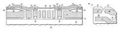
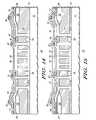
- a semiconductor device 10such as an accelerometer or other MEMS device, includes a semiconductor layer 12 , a buried oxide (BOX) layer 14 , a (semiconductor) active layer 16 , a (screen) oxide layer 18 and anchors 20 .
- the semiconductor layer 12is n-type monocrystalline silicon and is n-type
- the BOX layer 14is approximately 2 microns of silicon dioxide
- the active layer 16is approximately 0.4 microns of monocrystalline silicon.
- the semiconductor layer 12 , the BOX layer 18 and the active layer 16form a silicon-on-insulator substrate 11 .
- the semiconductor layer and the active layercan be any semiconductor material or combinations of materials, such as gallium arsenide, silicon germanium, silicon, monocrystalline silicon and the like and the BOX layer 14 can be any insulating material.
- the BOX layer 14is a sacrificial layer.
- the screen oxide layer 18is used as an etch stop layer during the formation of the anchors 20 .
- the screen oxide layer 18is approximately 0.12 microns in thickness of silicon dioxide; however, other oxides and thicknesses can be used.
- the anchors 20are a nitride, such as silicon nitride.
- silicon nitrideIn one embodiment approximately 0.8 microns of silicon nitride is deposited using low pressure chemical vapor deposition (LPCVD) over the semiconductor device 10 .
- LPCVDlow pressure chemical vapor deposition
- the silicon nitrideis etched back using the screen oxide layer 18 as an etch stop layer resulting in the silicon nitride formed on the screen oxide layer 18 being removed and the anchor 20 being recessed with respect to the screen oxide layer 18 and being approximately coplanar with the top of the active layer 16 .
- hydrofluoric acid (HF)is used to etch back the silicon nitride to form the anchors 20 .
- a dimple 23 and bulk contact openings 22are formed in layers 14 , 16 and 18 to expose the semiconductor layer 12 .
- the dimplesare approximately 1-2 microns in width.
- the screen oxide 18 , the active layer 16 and the BOX layer 14are completely etched through.
- the BOX layer 14is only partially etched.
- a time etchcan be used to remove approximately 0.5 microns of the BOX layer 14 .
- a timed etchis desirable (but not required) to stop within the BOX layer 14 and when forming the bulk contact openings 22 the semiconductor layer 12 can be used as an etch stop layer.
- the dimple 23is formed to prevent subsequently formed features, such as the seismic mass, from coming into contact with the semiconductor substrate and thereby prevents stiction. Stiction is a mode of failure that occurs when two surfaces come into contact and are held together by surface forces. This prevents any moving elements from moving in the semiconductor device 10 . In addition, the dimples may stop motion in the z-direction (i.e., the direction perpendicular to the ground) when the semiconductor device 10 is exposed to a high acceleration.
- the bulk contact openings 22(when filled with an appropriate material) will electrically coupled to the semiconductor substrate 10 to prevent the semiconductor layer 12 from being at a floating potential and thus it enables the substrate to be at a fixed potential. In addition, the bulk contact openings 22 (when filled with an appropriate material) will enable formation of an electromagnetic shield below subsequently formed layers.
- the screen oxide 18is removed by etching.
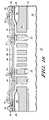
- an epitaxial semiconductor layer 24such as silicon, is grown from the semiconductor layer 12 through the bulk contacts 23 and from the active layer 16 , as shown in FIG. 3 . Since the active layer 16 and the epitaxial semiconductor layer 24 are the same materials, they combine together to form the epitaxial semiconductor layer 24 . In other words, the active layer 16 is the seed layer for the epitaxial growth of the epitaxial semiconductor layer 24 .
- the epitaxial semiconductor layer 24is grown to a required thickness of an accelerometer. In one embodiment, the epitaxial semiconductor layer 24 is approximately 25 microns thick and is n-type silicon doped with phosphorus.
- the epitaxial semiconductor layer 24is laterally grown over the dimple 23 in the BOX layer 14 due to the dimple 23 being a small feature even though the epitaxial growth is a selective process does not occur on the BOX layer 14 .
- the epitaxial semiconductor layer 24is formed over the anchors 20 and in the bulk contact openings 22 . So that the epitaxial semiconductor layer 24 grows in the dimples 23 and the over the anchors 20 the process conduction are chosen (as know to a skilled artisan) to render the process non-selective epitaxial growth.
- lateral growth of the epitaxial semiconductor layers 24occurs through epitaxial lateral overgrowth (ELO).
- isolation regions 26are formed to define an active area 17 of the semiconductor device 10 , which lies between field areas 19 , as shown in FIG. 4 .
- the isolation regions 26are within field areas 19 .
- the isolation regionsare formed using a LOCOS process as known to a skilled artisan; however, a shallow trench isolation process may also be used. It is desirable that the isolation regions 26 are thick (e.g., approximately 2-2.5 microns) to reduce parasitic capacitance of the active area 17 . If LOCOS is used, it is desirable that the slope of the bird's beak should be low so that resist layers used for patterning in subsequent processing have good step coverage.
- the distance from the isolation regions 26 to the active area 17should be large enough to prevent attack of the isolation regions 26 during a subsequently formed release; in one embodiment, the distance is approximately 5 to 20 microns. Furthermore, after the formation of the isolation regions 26 the semiconductor device 10 should not have excessive bow; in one embodiment, the bow is less than approximately 100 microns. In one embodiment, the oxide thermally grown to form the isolation regions 26 is approximately 0.05 microns.
- a first isolation nitride (layer) 28is deposited and patterned to remain over the isolation regions 26 , as shown in FIG. 4 , to protect the isolation regions 26 from the chemistry used during the release etch.
- the first isolation nitride 28is approximately 0.5 microns of a low stress silicon rich silicon nitride formed by LPCVD.
- the low stress silicon rich silicon nitridehas a tensile stress less than approximately 200 MPa.
- the first isolation nitride 28should have a high selectively to the BOX layer 14 , such 50:1 in an HF etch chemistry, for example.
- the patterningcan be formed using conventional processing (resist layers and an etch, such as reactive ion etching.) As shown in FIG. 4 , some of the first isolation nitride 28 may be formed over a portion of the active area 17 . In one embodiment, the overlap is approximately 10 microns by design but may vary due to processing.
- a patterning processis performed to form trenches 21 , 23 , 25 , 27 , 29 , 31 , 33 and 35 in the epitaxial semiconductor layer 24 .
- the patterningis performed by a deep reactive ion etch (DRIE) resulting in the trenchs' widths being approximately 1.8 to 2 microns, the minimum notching at the bottom of the trench being approximately 0 to 0.2 microns and the vertical sidewall of the trenches being approximately 89-90 degrees with respect to the semiconductor substrate 12 .
- the DRIEin one embodiment, etches down approximately 25 microns using the BOX layer 14 as an etch stop layer.
- a first sacrificial layer 40is formed and patterned over the semiconductor device 10 , as shown in FIG. 6 .
- the first sacrificial layer 40seals the trenches 21 , 23 , 25 , 27 , 29 , 31 , 33 and 35 by covering up the openings of the trenches 21 , 23 , 25 , 27 , 29 , 31 , 33 , and 35 and creates a top planar surface in the active area 17 .
- the first sacrificial layer 40may fill the trenches 21 , 23 , 25 , 27 , 29 , 31 , 33 , and 35 completely or partially depending on the conformality of the process used to form the first sacrificial layer 40 , especially when phosphosilicate glass (PSG) is used as the first sacrificial layer 40 and formed using PECVD.
- the trenches 21 , 23 , 25 , 27 , 29 , 31 , 33 , and 35are be filled with a key hold void but would be planar on the top surface of the trenches 21 , 23 , 25 , 27 , 29 , 31 , 33 , and 35 .
- the material chosen for the sacrificial layer 40should be able to withstand subsequent high temperature processing and be able to be removed without removing the layers which are to remain, as will be explained in more detail below.
- the sacrificial layer 40is of PSG.
- PSGis deposited using PECVD and is annealed in an N2, O2, or combination of the above environment to seal the top of the trenches 21 , 23 , 25 , 27 , 29 , 31 , 33 , and 35 .
- the patterning of the first sacrificial layer 40forms first openings 41 which expose portions of the first insulation nitride 28 , the fixed electrodes 34 so that subsequently formed bridges are coupled to the fixed electrodes 34 .
- the first sacrificial layer 40may be patterned using a resist layer and a wet etch, dry etch, or a combination of the above.
- bridges 42are formed over the semiconductor device 10 .
- the bridges 42couple the active area 17 to the field areas 19 and to bond pads (to be formed later) and thus are conductive.
- Any suitable materialcan be used that preferably has a low contact resistance (e.g., doped polysilicon with a contact resistance of approximately 20-40 Ohms/square), has good adhesion with the active area 17 , is not etched during a subsequently formed release etch, have low sheet resistance (e.g., doped polysilicon with a sheet resistance of approximately 20-50 Ohms/square), has sufficient mechanical strength to serve as the bridges after the release etch, and is able to withstand mechanical shocks.
- a low contact resistancee.g., doped polysilicon with a contact resistance of approximately 20-40 Ohms/square
- have low sheet resistancee.g., doped polysilicon with a sheet resistance of approximately 20-50 Ohms/square
- the bridges 42are formed of polysilicon using the following processes. First, a clean process using HF may be performed to remove any native oxide from the exposed portions of the fixed electrodes 34 . Next, approximately two microns of polysilicon is deposited using LPCVD so that it is compressive. The polysilicon layer 42 is patterned by etching using phosphorus. The polysilicon layer 42 is then etched using conventional processing using the first sacrificial layer 40 and the first isolation nitride 28 as etch stop layers.
- second isolation nitrides (layers) 44are formed over portions of the bridges 42 , as shown in FIG. 8 .
- the second isolation nitrides 44electrically isolate in the active area 17 the bridges 42 , which preferably include polysilicon, from the subsequently formed cap layer, which is also preferably made of polysilicon.
- the second isolation nitrides 44should be thick enough to not be entirely removed during the later performed release etch if they are etched at all. In one embodiment, the second isolation nitrides 44 are approximately 0.5 to 1 micron of low stress silicon rich silicon nitride formed by LPCVD.
- the low stress silicon rich silicon nitridehas a tensile stress less than approximately 200 MPa. Any known patterning process can be used.
- a second sacrificial layer 46is formed over the semiconductor device 10 , as shown in FIG. 9 .
- the second sacrificial layer 46defines the spacing of the accelerometer to the subsequently formed cap layer. The spacing should be large enough to reduce parasitic capacitance.
- the second sacrificial layer 46forms both lateral and z-axis stops and exposes pillars 45 for supports for the (to be formed ) cap layer.
- the second sacrificial layer 46is formed by PECVD, LPCVD, CVD, physical vapor deposition (PVD), the like, and combinations of the above.
- the second sacrificial layer 46is approximately 1-3 microns of PSG.
- pillars 45are formed by forming etch holes in the second sacrificial layer 46 .
- the pillars 45make the subsequently formed cap layer stronger.
- the maximum pressure that will be exerted on the semiconductor device 10should be used. Usually, the spacing of the pillars will be approximately 20 to 50 microns apart.
- a cap layer 48is formed over the semiconductor device 10 and the second sacrificial layer 46 .
- the cap layer 48is formed over the pillars 45 , which will become the mechanical support for the cap layer 48 after the release etch, which will remove the first and second sacrificial layers 40 and 46 and BOX layer 14 .
- the cap layer 48should be thick enough and the density of the pillars 45 should be great enough so that the cap layer 48 can withstand pressures of generated when the semiconductor device 10 is packaged, for example by plastic molding. For plastic molding, such pressures are approximately 1000 psi.
- the cap layer 48is approximately 2 to 10 microns of polysilicon formed by LPCVD or an epitaxial process.
- the polysiliconmay be annealed after deposition to decrease stress in the material.
- Other materialssuch as germanium and any metal can be used instead of or in conjunction with polysilicon.
- any material with suitable mechanical strength and that is compatible with CMOS processingcan be used.
- holes (i.e., openings) 43are etched in the cap layer 48 , as shown in FIG. 11 . Any conventional etch process can be used.
- the holes 43are used to allow the chemicals used in the release etch to reach the first 40 and second 46 sacrificial layers and the BOX layer 14 so that at least portions of these layers are removed to release the semiconductor device 10 .
- the release etchis performed to release the seismic mass 32 by removing the first 40 and the second 46 sacrificial layers and a portion of the BOX layer 14 and forming a gap 50 , as shown in FIG. 11 . It may be desirable to perform an overetch to account for variations across a wafer to ensure complete removal of the first 40 and the second 46 sacrificial layers and the portions of the BOX layer 14 .
- the release etch chemistry chosenpreferably minimizes the etching of the anchors 20 and the second isolation nitride 44 .
- the resulting structurepreferably has no stiction in the x, y and z directions between any moving and fixed parts.
- the release etchremoves the first 40 and the second 46 sacrificial layers below the cap 48 and within the trenches 21 , 23 , 25 , 27 , 29 , 31 , 33 and 35 .
- the BOX layer 14is removed from below the trenches 21 , 23 , 25 , 27 , 29 , 31 , 33 and 35 , the fixed electrodes 34 , the suspension 30 , the bulk contact 32 , and the seismic mass 36 .
- the BOX layer 14is removed from at least the majority of the active area 17 .
- a hydrofluoric acid (HF) wet etchis used to remove the first 40 and second 46 sacrificial layers and portion of the BOX layer 14 .
- the holes 43are sealed by forming a reflowable layer 51 over the semiconductor device 10 , as shown in FIG. 12 .
- the area enclosed in the circle 49 of FIG. 11is shown in FIG. 12 after the reflowable layer 51 is formed.
- the reflowable layer 51can be deposited by PECVD, physical vapor deposition (PVD) or atmospheric CVD. (Atmospheric CVD is CVD at a pressure approximately equal to atmosphere.)
- the thickness of the reflowable layer 51may depend on the etch port width and height and the thickness of the cap layer 48 . In one embodiment, the cap layer 48 is approximately 2-4 microns in thickness. As illustrated in FIG. 12 , the reflowable layer 51 does not seal the hole 43 .
- the reflowable layer 51is formed on the top surface of the cap layer 48 and the sidewalls of the hole 43 . Thus, subsequent processing needs to occur so that the reflowable layer 51 seals the hole 43 .
- the reflowable layer 51is PSG; any other suitable material may be used.
- the reflowable layer 51is approximately 3 microns of PSG.
- the reflowable layer 51is borophosphosilicate glass (BPSG).
- the pressure within the gap 50is at approximately atmospheric pressure to prevent oscillation of the accelerometer (i.e., the accelerometer is overdamped.) If instead, the gap 50 is at vacuum pressure oscillation will undesirably occur.
- the process used to form the reflowable layeroccurs at vacuum, which is the case for PECVD
- the semiconductor device 10 at this point in processingis removed from the vacuum and put into an atmosphere which has a pressure approximately equal to atmospheric pressure for subsequent processing.
- the resulting sealshould be hermetic and should not encroach the device area (i.e., the area underneath the cap layer 48 ).
- the reflowable layer 51is reflowed in a pressure approximately equal to atmosphere, in one embodiment using an anneal process.
- the temperatureis between approximately 1,000 and 1,040 degrees Celsius with approximately 4-8%, preferably approximately 6.5%, of phosphorus in the atmosphere.
- the topography of the semiconductor device 10may alter the parameters used for the anneal.
- the annealmay occur on a global scale so that the entire semiconductor device 10 is exposed to the heat, such as by using a furnace. Instead, the anneal can occur on a local scale (i.e., localized annealing) so that only one area is exposed to the heat and not the entire semiconductor device 10 .
- a lasermay be used.
- phosphorusmay be added to the atmosphere to decrease the temperature at which the anneal occurs; it is not necessary that phosphorus be present.
- Chemicalssuch as POCl 3 and PH 3 can be used in a furnace to introduce phosphorus into the atmosphere.
- the reflowable layer 51has sealed the hole 43 , made the pressure of the gap 50 approximately equal to atmospheric pressure and formed the seal layer 52 , as shown in FIG. 13 .
- the reflowable layer 51has established the pressure in the gap 50 and the holes 43 at approximately atmospheric pressure and has closed the gap 50 and holes off to the environment.
- the accelerometeris now desirably overdamped.
- the reflow or anneal process to form the seal layer 52occurs in an N 2 , O 2 , or combination of the above environment at approximately 1000-1040 degrees Celsius.
- a densification anneal processmay be performed prior to the reflow anneal process at approximately 900-1000 degrees Celsius an N 2 , O 2 , or combination of the above environment.
- the seal layer 52is patterned using an RIE process with the cap layer 48 as an etch stop layer.
- the reflow or anneal processmay not be performed. If a process that can deposit the seal layer 52 at approximately atmospheric pressure to seal the hole 43 is used, then the reflow or anneal process is not needed. For example, atmospheric CVD may be used. However, to seal the hole 43 using atmospheric CVD a thicker seal layer 52 may need to be deposited so that reflowing is not needed. In one embodiment, reflow may occur using a high pressure oxidation furnace (HiPOX) furnace.
- HiPOXhigh pressure oxidation furnace
- a cap seal layer 54which may be one or more layers, is formed to hermetically encase the seal layer 52 over the holes 43 , as shown in FIG. 15 . It is desirable that the thickness of the cap seal layer 54 is be sufficient to prevent access of the seal layer 52 to the atmosphere, even in a high humidity and high temperature environment if the semiconductor device 10 will later be put in such an environment.
- the cap seal layer 54can be any conductive material and preferably has a low stress and a low contact resistance to the cap layer 48 . In one embodiment, cap seal has a stress less than approximately 100 MPa and a contact resistance less than approximately 20-40 Ohms/square. In one embodiment, the cap seal layer 54 is approximately 0.3 to 3 microns of polysilicon deposited using LPCVD. The polysilicon may be doped and subsequently annealed to decrease stress.
- bond pads 56are formed. It is desirable that the bond pads form a good metal contact with the underlying materials (such as the cap seal layer 54 ), are suitable materials for good adhesion for wirebonds or other electrical connections formed during packaging processes, and have a clean surface for subsequent processing.
- approximately 2 microns of Al/Siis sputtered over the semiconductor device 10 and an etch using the cap seal layer 54 as an etch stop layer is preformed to pattern the sputtered Al/Si layer and form the bond pads 56 .
- an etch(using conventional processing) is performed to remove portions of the cap seal layer 54 and the cap layer 48 from the field areas 19 .
- subsequent processingoccurs to package the semiconductor device 10 .
- subsequent processingoccurs to package the semiconductor device 10 . Since such processing is known to a skilled artisan and may distract from the present invention such is not discussed herein.
- a process for forming a seal and cap sealuses a single wafer or substrate and seals the gap at approximately atmospheric pressure. Furthermore, the process uses an on-chip cap process. By doing so, the due size of the semiconductor device 10 is decreased compared to when a wafer is used as the cap.
- Benefits, other advantages, and solutions to problemshave been described above with regard to specific embodiments. However, the benefits, advantages, solutions to problems, and any element(s) that may cause any benefit, advantage, or solution to occur or become more pronounced are not to be construed as a critical, required, or essential feature or element of any or all the claims.
- the seal layercould be a solder ball (e.g., made of Pb/Sn) or any volume of material, for example, that is deposited over the openings and is later optionally reflowed to form the seal layer 52 .
- solder balle.g., made of Pb/Sn
- any volume of materialfor example, that is deposited over the openings and is later optionally reflowed to form the seal layer 52 .
- p-type materialscould also be used. Accordingly, the specification and figures are to be regarded in an illustrative rather than a restrictive sense, and all such modifications are intended to be included within the scope of the present invention.
- the terms “front”, “back”, “top”, “bottom”, “over”, “under” and the like in the description and in the claims, if any,are used for descriptive purposes and not necessarily for describing permanent relative positions. It is understood that the terms so used are interchangeable under appropriate circumstances such that the embodiments of the invention described herein are, for example, capable of operation in other orientations than those illustrated or otherwise described herein.
- the terms “comprises,” “comprising,” or any other variation thereof,are intended to cover a non-exclusive inclusion, such that a process, method, article, or apparatus that comprises a list of elements does not include only those elements but may include other elements not expressly listed or inherent to such process, method, article, or apparatus.
- the terms “a” or “an”, as used herein,are defined as one or more than one.
- the term “coupled”, as used herein,is defined as connected, although not necessarily directly, and not necessarily mechanically.
Landscapes
- Engineering & Computer Science (AREA)
- Microelectronics & Electronic Packaging (AREA)
- Manufacturing & Machinery (AREA)
- Micromachines (AREA)
Abstract
Description
Claims (20)
Priority Applications (1)
| Application Number | Priority Date | Filing Date | Title |
|---|---|---|---|
| US10/730,230US7585744B2 (en) | 2003-12-08 | 2003-12-08 | Method of forming a seal for a semiconductor device |
Applications Claiming Priority (1)
| Application Number | Priority Date | Filing Date | Title |
|---|---|---|---|
| US10/730,230US7585744B2 (en) | 2003-12-08 | 2003-12-08 | Method of forming a seal for a semiconductor device |
Publications (2)
| Publication Number | Publication Date |
|---|---|
| US20050124089A1 US20050124089A1 (en) | 2005-06-09 |
| US7585744B2true US7585744B2 (en) | 2009-09-08 |
Family
ID=34634113
Family Applications (1)
| Application Number | Title | Priority Date | Filing Date |
|---|---|---|---|
| US10/730,230Expired - Fee RelatedUS7585744B2 (en) | 2003-12-08 | 2003-12-08 | Method of forming a seal for a semiconductor device |
Country Status (1)
| Country | Link |
|---|---|
| US (1) | US7585744B2 (en) |
Cited By (10)
| Publication number | Priority date | Publication date | Assignee | Title |
|---|---|---|---|---|
| US20080119001A1 (en)* | 2006-11-17 | 2008-05-22 | Charles Grosjean | Substrate contact for a mems device |
| US20090311819A1 (en)* | 2007-10-18 | 2009-12-17 | Tso-Chi Chang | Method for Making Micro-Electromechanical System Devices |
| US20100213568A1 (en)* | 2009-02-24 | 2010-08-26 | PixArt Imaging Incorporation, R.O.C. | Micro-electro-mechanical-system device with guard ring and method for making same |
| US20110147860A1 (en)* | 2009-12-22 | 2011-06-23 | Commissariat A L'energie Atomique Et Aux Ene Alt | Micromechanical structure comprising a mobile part having stops for out-of-plane displacements of the structure and its production process |
| US20120001277A1 (en)* | 2010-06-30 | 2012-01-05 | Woo Tae Park | Methods for making in-plane and out-of-plane sensing micro-electro-mechanical systems (mems) |
| US8603889B2 (en) | 2012-03-30 | 2013-12-10 | International Business Machines Corporation | Integrated circuit structure having air-gap trench isolation and related design structure |
| US8648432B2 (en)* | 2011-11-28 | 2014-02-11 | Texas Instruments Deutschland Gmbh | Fully embedded micromechanical device, system on chip and method for manufacturing the same |
| US9266717B2 (en) | 2013-03-15 | 2016-02-23 | Versana Micro Inc | Monolithically integrated multi-sensor device on a semiconductor substrate and method therefor |
| US11365117B2 (en) | 2019-12-23 | 2022-06-21 | Industrial Technology Research Institute | MEMS device and manufacturing method of the same |
| US11939212B2 (en) | 2019-12-23 | 2024-03-26 | Industrial Technology Research Institute | MEMS device, manufacturing method of the same, and integrated MEMS module using the same |
Families Citing this family (15)
| Publication number | Priority date | Publication date | Assignee | Title |
|---|---|---|---|---|
| US7098065B2 (en)* | 2004-09-28 | 2006-08-29 | Stmicroelectronics, Inc. | Integrated lid formed on MEMS device |
| JP4544140B2 (en)* | 2005-02-16 | 2010-09-15 | セイコーエプソン株式会社 | MEMS element |
| US7824943B2 (en) | 2006-06-04 | 2010-11-02 | Akustica, Inc. | Methods for trapping charge in a microelectromechanical system and microelectromechanical system employing same |
| US20080119002A1 (en)* | 2006-11-17 | 2008-05-22 | Charles Grosjean | Substrate contact for a MEMS device |
| DE102008040851A1 (en) | 2008-07-30 | 2010-02-04 | Robert Bosch Gmbh | Method for capping a MEMS wafer and MEMS wafer |
| US8956903B2 (en) | 2010-06-25 | 2015-02-17 | International Business Machines Corporation | Planar cavity MEMS and related structures, methods of manufacture and design structures |
| CN102637628A (en)* | 2011-02-10 | 2012-08-15 | 上海宏力半导体制造有限公司 | Reduction method of dielectric capacitance |
| JP5760502B2 (en)* | 2011-02-25 | 2015-08-12 | 富士通株式会社 | Electronic device and manufacturing method thereof |
| US20140138790A1 (en) | 2012-11-21 | 2014-05-22 | Spansion Llc | Inter-Layer Insulator for Electronic Devices and Apparatus for Forming Same |
| JP6269113B2 (en)* | 2014-02-03 | 2018-01-31 | セイコーエプソン株式会社 | MEMS device and manufacturing method thereof |
| JP2015171740A (en)* | 2014-03-12 | 2015-10-01 | セイコーエプソン株式会社 | MEMS device and manufacturing method thereof |
| CN114553182A (en)* | 2020-11-24 | 2022-05-27 | 联华电子股份有限公司 | Surface acoustic wave module structure and manufacturing method thereof |
| US11545577B2 (en)* | 2020-12-08 | 2023-01-03 | Globalfoundries U.S. Inc. | Semiconductor structure with in-device high resistivity polycrystalline semiconductor element and method |
| CN113675327B (en)* | 2021-07-23 | 2025-02-14 | 无锡莱斯能特科技有限公司 | A method for manufacturing a thermopile sensor |
| US20250187901A1 (en)* | 2023-12-08 | 2025-06-12 | Lawrence Semiconductor Research Laboratory, Inc. | Micro-electro-mechanical systems (mems) having vertical stops and anchor structures |
Citations (21)
| Publication number | Priority date | Publication date | Assignee | Title |
|---|---|---|---|---|
| US5208180A (en)* | 1992-03-04 | 1993-05-04 | Micron Technology, Inc. | Method of forming a capacitor |
| US5576250A (en)* | 1992-12-28 | 1996-11-19 | Commissariat A L'energie Atomique | Process for the production of accelerometers using silicon on insulator technology |
| US5798283A (en)* | 1995-09-06 | 1998-08-25 | Sandia Corporation | Method for integrating microelectromechanical devices with electronic circuitry |
| US5869406A (en)* | 1995-09-28 | 1999-02-09 | Mosel Vitelic, Inc. | Method for forming insulating layers between polysilicon layers |
| US5911109A (en)* | 1994-07-12 | 1999-06-08 | National Semiconductor Corporation | Method of forming an integrated circuit including filling and planarizing a trench having an oxygen barrier layer |
| US6013584A (en)* | 1997-02-19 | 2000-01-11 | Applied Materials, Inc. | Methods and apparatus for forming HDP-CVD PSG film used for advanced pre-metal dielectric layer applications |
| US20020016058A1 (en)* | 2000-06-15 | 2002-02-07 | Bin Zhao | Microelectronic air-gap structures and methods of forming the same |
| US6413793B1 (en)* | 2001-05-17 | 2002-07-02 | Xerox Corporation | Method of forming protrusions on single crystal silicon structures built on silicon-on-insulator wafers |
| US20020098611A1 (en)* | 2000-11-18 | 2002-07-25 | Pei-Zen Chang | Micro-electromechanical process for fabrication of integrated multi-frequency communication passive components |
| US20020182819A1 (en)* | 1999-11-22 | 2002-12-05 | Martin Schrems | Method for fabricating an insulation collar in a trench capacitor |
| US6617657B1 (en)* | 1998-05-08 | 2003-09-09 | Rockwell Automation Technologies, Inc. | Process for manufacture of micro electromechanical devices having high electrical isolation |
| US6629425B2 (en)* | 2000-07-24 | 2003-10-07 | Micron Technology, Inc. | MEMS heat pumps for integrated circuit heat dissipation |
| US6635509B1 (en) | 2002-04-12 | 2003-10-21 | Dalsa Semiconductor Inc. | Wafer-level MEMS packaging |
| US20040058476A1 (en)* | 2002-09-25 | 2004-03-25 | Ziptronix | Wafer bonding hermetic encapsulation |
| US20040119125A1 (en)* | 2002-12-23 | 2004-06-24 | Motorola Inc. | Semiconductor structure and method of manufacture |
| US20040180465A1 (en)* | 2001-08-31 | 2004-09-16 | Superconductor Technologies, Inc. | Method of making an electrostatic actuator |
| US20050023629A1 (en)* | 2003-07-31 | 2005-02-03 | Xiaoyi Ding | Wafer-level sealed microdevice having trench isolation and methods for making the same |
| US6936491B2 (en)* | 2003-06-04 | 2005-08-30 | Robert Bosch Gmbh | Method of fabricating microelectromechanical systems and devices having trench isolated contacts |
| US7098065B2 (en)* | 2004-09-28 | 2006-08-29 | Stmicroelectronics, Inc. | Integrated lid formed on MEMS device |
| US20070138584A1 (en)* | 2004-09-20 | 2007-06-21 | General Electric Company | Microelectromechanical system pressure sensor and method for making and using |
| US20070298534A1 (en)* | 2002-12-27 | 2007-12-27 | Matsushita Electric Industrial Co., Ltd. | Electronic device and method of manufacturing the same |
- 2003
- 2003-12-08USUS10/730,230patent/US7585744B2/ennot_activeExpired - Fee Related
Patent Citations (21)
| Publication number | Priority date | Publication date | Assignee | Title |
|---|---|---|---|---|
| US5208180A (en)* | 1992-03-04 | 1993-05-04 | Micron Technology, Inc. | Method of forming a capacitor |
| US5576250A (en)* | 1992-12-28 | 1996-11-19 | Commissariat A L'energie Atomique | Process for the production of accelerometers using silicon on insulator technology |
| US5911109A (en)* | 1994-07-12 | 1999-06-08 | National Semiconductor Corporation | Method of forming an integrated circuit including filling and planarizing a trench having an oxygen barrier layer |
| US5798283A (en)* | 1995-09-06 | 1998-08-25 | Sandia Corporation | Method for integrating microelectromechanical devices with electronic circuitry |
| US5869406A (en)* | 1995-09-28 | 1999-02-09 | Mosel Vitelic, Inc. | Method for forming insulating layers between polysilicon layers |
| US6013584A (en)* | 1997-02-19 | 2000-01-11 | Applied Materials, Inc. | Methods and apparatus for forming HDP-CVD PSG film used for advanced pre-metal dielectric layer applications |
| US6617657B1 (en)* | 1998-05-08 | 2003-09-09 | Rockwell Automation Technologies, Inc. | Process for manufacture of micro electromechanical devices having high electrical isolation |
| US20020182819A1 (en)* | 1999-11-22 | 2002-12-05 | Martin Schrems | Method for fabricating an insulation collar in a trench capacitor |
| US20020016058A1 (en)* | 2000-06-15 | 2002-02-07 | Bin Zhao | Microelectronic air-gap structures and methods of forming the same |
| US6629425B2 (en)* | 2000-07-24 | 2003-10-07 | Micron Technology, Inc. | MEMS heat pumps for integrated circuit heat dissipation |
| US20020098611A1 (en)* | 2000-11-18 | 2002-07-25 | Pei-Zen Chang | Micro-electromechanical process for fabrication of integrated multi-frequency communication passive components |
| US6413793B1 (en)* | 2001-05-17 | 2002-07-02 | Xerox Corporation | Method of forming protrusions on single crystal silicon structures built on silicon-on-insulator wafers |
| US20040180465A1 (en)* | 2001-08-31 | 2004-09-16 | Superconductor Technologies, Inc. | Method of making an electrostatic actuator |
| US6635509B1 (en) | 2002-04-12 | 2003-10-21 | Dalsa Semiconductor Inc. | Wafer-level MEMS packaging |
| US20040058476A1 (en)* | 2002-09-25 | 2004-03-25 | Ziptronix | Wafer bonding hermetic encapsulation |
| US20040119125A1 (en)* | 2002-12-23 | 2004-06-24 | Motorola Inc. | Semiconductor structure and method of manufacture |
| US20070298534A1 (en)* | 2002-12-27 | 2007-12-27 | Matsushita Electric Industrial Co., Ltd. | Electronic device and method of manufacturing the same |
| US6936491B2 (en)* | 2003-06-04 | 2005-08-30 | Robert Bosch Gmbh | Method of fabricating microelectromechanical systems and devices having trench isolated contacts |
| US20050023629A1 (en)* | 2003-07-31 | 2005-02-03 | Xiaoyi Ding | Wafer-level sealed microdevice having trench isolation and methods for making the same |
| US20070138584A1 (en)* | 2004-09-20 | 2007-06-21 | General Electric Company | Microelectromechanical system pressure sensor and method for making and using |
| US7098065B2 (en)* | 2004-09-28 | 2006-08-29 | Stmicroelectronics, Inc. | Integrated lid formed on MEMS device |
Non-Patent Citations (6)
| Title |
|---|
| Burns et al., "Sealed-cavity Resonant Microbeam Accelerometer," Sensors and Actuators 1 53 (1996), pp. 249-255. |
| Gogoi et al., "A Low-Voltage Force-Balanced Pressure Sensor With Hermetically Sealed Servomechanism," IEEE 1999, pp. 493-498. |
| Lin et al., "Microelectromechanical Filters for Signal Processing," IEEE Journal Of Microelectromechanical Systems, vol. 7, No. 3, Sep. 1998, pp. 286-294. |
| Sze, S.M., "VLSI Technology", 1988 by Bell Telephone Laboratories, Inc., McGraw-Hill, pp. 355-362.* |
| U.S. Appl. No. 10/328,922, filed Dec. 23, 2002. |
| U.S. Appl. No. 10/328,923, filed Dec. 23, 2002. |
Cited By (23)
| Publication number | Priority date | Publication date | Assignee | Title |
|---|---|---|---|---|
| US20080119001A1 (en)* | 2006-11-17 | 2008-05-22 | Charles Grosjean | Substrate contact for a mems device |
| US20090311819A1 (en)* | 2007-10-18 | 2009-12-17 | Tso-Chi Chang | Method for Making Micro-Electromechanical System Devices |
| US7824945B2 (en)* | 2007-10-18 | 2010-11-02 | Asia Pacific Microsystems, Inc. | Method for making micro-electromechanical system devices |
| US9018718B2 (en)* | 2009-02-24 | 2015-04-28 | Pixart Imaging Incorporation | Micro-electro-mechanical-system device with guard ring and method for making same |
| US20100213568A1 (en)* | 2009-02-24 | 2010-08-26 | PixArt Imaging Incorporation, R.O.C. | Micro-electro-mechanical-system device with guard ring and method for making same |
| US20110147860A1 (en)* | 2009-12-22 | 2011-06-23 | Commissariat A L'energie Atomique Et Aux Ene Alt | Micromechanical structure comprising a mobile part having stops for out-of-plane displacements of the structure and its production process |
| US9061895B2 (en)* | 2009-12-22 | 2015-06-23 | Commissariat à l'énergie atomique et aux énergies alternatives | Micromechanical structure comprising a mobile part having stops for out-of plane displacements of the structure and its production process |
| US20120001277A1 (en)* | 2010-06-30 | 2012-01-05 | Woo Tae Park | Methods for making in-plane and out-of-plane sensing micro-electro-mechanical systems (mems) |
| US8461656B2 (en)* | 2010-06-30 | 2013-06-11 | Freescale Semiconductor, Inc. | Device structures for in-plane and out-of-plane sensing micro-electro-mechanical systems (MEMS) |
| US8648432B2 (en)* | 2011-11-28 | 2014-02-11 | Texas Instruments Deutschland Gmbh | Fully embedded micromechanical device, system on chip and method for manufacturing the same |
| US8872305B2 (en) | 2012-03-30 | 2014-10-28 | International Business Machines Corporation | Integrated circuit structure having air-gap trench isolation and related design structure |
| US8603889B2 (en) | 2012-03-30 | 2013-12-10 | International Business Machines Corporation | Integrated circuit structure having air-gap trench isolation and related design structure |
| US9580302B2 (en) | 2013-03-15 | 2017-02-28 | Versana Micro Inc. | Cell phone having a monolithically integrated multi-sensor device on a semiconductor substrate and method therefor |
| US9327965B2 (en) | 2013-03-15 | 2016-05-03 | Versana Micro Inc | Transportation device having a monolithically integrated multi-sensor device on a semiconductor substrate and method therefor |
| US9266717B2 (en) | 2013-03-15 | 2016-02-23 | Versana Micro Inc | Monolithically integrated multi-sensor device on a semiconductor substrate and method therefor |
| US9758368B2 (en) | 2013-03-15 | 2017-09-12 | Versana Micro Inc | Monolithically integrated multi-sensor device on a semiconductor substrate and method therefor |
| US9862594B2 (en) | 2013-03-15 | 2018-01-09 | Versana Micro Inc. | Wearable device having a monolithically integrated multi-sensor device on a semiconductor substrate and method therefor |
| US9890038B2 (en) | 2013-03-15 | 2018-02-13 | Versana Micro Inc. | Monolithically integrated multi-sensor device on a semiconductor substrate and method therefor |
| US10280074B2 (en) | 2013-03-15 | 2019-05-07 | Versana Micro Inc | Monolithically integrated multi-sensor device on a semiconductor substrate and method therefor |
| US10508026B2 (en) | 2013-03-15 | 2019-12-17 | Versana Micro Inc. | Monolithically integrated multi-sensor device on a semiconductor substrate and method therefor |
| US11174154B2 (en) | 2013-03-15 | 2021-11-16 | Versana Micro Inc. | Monolithically integrated multi-sensor device on a semiconductor substrate and method therefor |
| US11365117B2 (en) | 2019-12-23 | 2022-06-21 | Industrial Technology Research Institute | MEMS device and manufacturing method of the same |
| US11939212B2 (en) | 2019-12-23 | 2024-03-26 | Industrial Technology Research Institute | MEMS device, manufacturing method of the same, and integrated MEMS module using the same |
Also Published As
| Publication number | Publication date |
|---|---|
| US20050124089A1 (en) | 2005-06-09 |
Similar Documents
| Publication | Publication Date | Title |
|---|---|---|
| US7585744B2 (en) | Method of forming a seal for a semiconductor device | |
| US7923278B2 (en) | Integrated getter area for wafer level encapsulated microelectromechanical systems | |
| US6951824B2 (en) | Method for manufacturing a micromechanical component and a component that is manufactured in accordance with the method | |
| US8058143B2 (en) | Substrate bonding with metal germanium silicon material | |
| US9725304B2 (en) | Method to package multiple MEMS sensors and actuators at different gases and cavity pressures | |
| US7041225B2 (en) | Micromechanical component and method for producing the same | |
| EP1633673B1 (en) | Method for fabricating microelectromechanical systems having trench isolated contacts | |
| US9617150B2 (en) | Micro-electro mechanical system (MEMS) device having a blocking layer formed between closed chamber and a dielectric layer of a CMOS substrate | |
| US7259436B2 (en) | Micromechanical component and corresponding production method | |
| US9840410B2 (en) | Micromechanical component | |
| US20220348455A1 (en) | Systems and methods for providing getters in microelectromechanical systems | |
| US20150284240A1 (en) | Structures and formation methods of micro-electro mechanical system device | |
| US8704317B2 (en) | Microstructure device with an improved anchor | |
| US9487391B2 (en) | Micro-electro mechanical system (MEMS) device having a blocking layer formed between closed chamber and a dielectric layer of a CMOS substrate | |
| US8461656B2 (en) | Device structures for in-plane and out-of-plane sensing micro-electro-mechanical systems (MEMS) | |
| US20130230939A1 (en) | High aspect ratio mems devices and methods for forming the same | |
| US9266721B2 (en) | Eutectic bonding of thin chips on a carrier substrate | |
| JP2024152674A (en) | Double layer MEMS device and method of manufacture - Patents.com | |
| US7063796B2 (en) | Micromechanical component and method for producing the same | |
| KR101988469B1 (en) | MEMS sensor and Method for fabricating of the same | |
| CN118062806B (en) | MEMS device and preparation method thereof |
Legal Events
| Date | Code | Title | Description |
|---|---|---|---|
| AS | Assignment | Owner name:MOTOROLA, INC., ILLINOIS Free format text:ASSIGNMENT OF ASSIGNORS INTEREST;ASSIGNORS:GOGOI, BISHNU P.;ROOP, RAYMOND M.;REEL/FRAME:014779/0261 Effective date:20031206 | |
| AS | Assignment | Owner name:FREESCALE SEMICONDUCTOR, INC., TEXAS Free format text:ASSIGNMENT OF ASSIGNORS INTEREST;ASSIGNOR:MOTOROLA, INC;REEL/FRAME:015360/0718 Effective date:20040404 Owner name:FREESCALE SEMICONDUCTOR, INC.,TEXAS Free format text:ASSIGNMENT OF ASSIGNORS INTEREST;ASSIGNOR:MOTOROLA, INC;REEL/FRAME:015360/0718 Effective date:20040404 | |
| AS | Assignment | Owner name:MOTOROLA, INC., ILLINOIS Free format text:ASSIGNMENT OF ASSIGNORS INTEREST;ASSIGNORS:GOGOI, BISHNU P.;ROOP, RAYMOND M.;DESAI, HEMANT D.;REEL/FRAME:016319/0175 Effective date:20050518 | |
| AS | Assignment | Owner name:CITIBANK, N.A. AS COLLATERAL AGENT, NEW YORK Free format text:SECURITY AGREEMENT;ASSIGNORS:FREESCALE SEMICONDUCTOR, INC.;FREESCALE ACQUISITION CORPORATION;FREESCALE ACQUISITION HOLDINGS CORP.;AND OTHERS;REEL/FRAME:018855/0129 Effective date:20061201 Owner name:CITIBANK, N.A. AS COLLATERAL AGENT,NEW YORK Free format text:SECURITY AGREEMENT;ASSIGNORS:FREESCALE SEMICONDUCTOR, INC.;FREESCALE ACQUISITION CORPORATION;FREESCALE ACQUISITION HOLDINGS CORP.;AND OTHERS;REEL/FRAME:018855/0129 Effective date:20061201 | |
| STCF | Information on status: patent grant | Free format text:PATENTED CASE | |
| AS | Assignment | Owner name:CITIBANK, N.A.,NEW YORK Free format text:SECURITY AGREEMENT;ASSIGNOR:FREESCALE SEMICONDUCTOR, INC.;REEL/FRAME:023882/0834 Effective date:20091030 Owner name:CITIBANK, N.A., NEW YORK Free format text:SECURITY AGREEMENT;ASSIGNOR:FREESCALE SEMICONDUCTOR, INC.;REEL/FRAME:023882/0834 Effective date:20091030 | |
| AS | Assignment | Owner name:CITIBANK, N.A., AS COLLATERAL AGENT,NEW YORK Free format text:SECURITY AGREEMENT;ASSIGNOR:FREESCALE SEMICONDUCTOR, INC.;REEL/FRAME:024397/0001 Effective date:20100413 Owner name:CITIBANK, N.A., AS COLLATERAL AGENT, NEW YORK Free format text:SECURITY AGREEMENT;ASSIGNOR:FREESCALE SEMICONDUCTOR, INC.;REEL/FRAME:024397/0001 Effective date:20100413 | |
| FPAY | Fee payment | Year of fee payment:4 | |
| AS | Assignment | Owner name:CITIBANK, N.A., AS NOTES COLLATERAL AGENT, NEW YORK Free format text:SECURITY AGREEMENT;ASSIGNOR:FREESCALE SEMICONDUCTOR, INC.;REEL/FRAME:030633/0424 Effective date:20130521 Owner name:CITIBANK, N.A., AS NOTES COLLATERAL AGENT, NEW YOR Free format text:SECURITY AGREEMENT;ASSIGNOR:FREESCALE SEMICONDUCTOR, INC.;REEL/FRAME:030633/0424 Effective date:20130521 | |
| AS | Assignment | Owner name:CITIBANK, N.A., AS NOTES COLLATERAL AGENT, NEW YORK Free format text:SECURITY AGREEMENT;ASSIGNOR:FREESCALE SEMICONDUCTOR, INC.;REEL/FRAME:031591/0266 Effective date:20131101 Owner name:CITIBANK, N.A., AS NOTES COLLATERAL AGENT, NEW YOR Free format text:SECURITY AGREEMENT;ASSIGNOR:FREESCALE SEMICONDUCTOR, INC.;REEL/FRAME:031591/0266 Effective date:20131101 | |
| AS | Assignment | Owner name:FREESCALE SEMICONDUCTOR, INC., TEXAS Free format text:PATENT RELEASE;ASSIGNOR:CITIBANK, N.A., AS COLLATERAL AGENT;REEL/FRAME:037354/0854 Effective date:20151207 Owner name:FREESCALE SEMICONDUCTOR, INC., TEXAS Free format text:PATENT RELEASE;ASSIGNOR:CITIBANK, N.A., AS COLLATERAL AGENT;REEL/FRAME:037354/0225 Effective date:20151207 Owner name:FREESCALE SEMICONDUCTOR, INC., TEXAS Free format text:PATENT RELEASE;ASSIGNOR:CITIBANK, N.A., AS COLLATERAL AGENT;REEL/FRAME:037356/0553 Effective date:20151207 Owner name:FREESCALE SEMICONDUCTOR, INC., TEXAS Free format text:PATENT RELEASE;ASSIGNOR:CITIBANK, N.A., AS COLLATERAL AGENT;REEL/FRAME:037356/0143 Effective date:20151207 | |
| AS | Assignment | Owner name:MORGAN STANLEY SENIOR FUNDING, INC., MARYLAND Free format text:ASSIGNMENT AND ASSUMPTION OF SECURITY INTEREST IN PATENTS;ASSIGNOR:CITIBANK, N.A.;REEL/FRAME:037486/0517 Effective date:20151207 | |
| AS | Assignment | Owner name:MORGAN STANLEY SENIOR FUNDING, INC., MARYLAND Free format text:ASSIGNMENT AND ASSUMPTION OF SECURITY INTEREST IN PATENTS;ASSIGNOR:CITIBANK, N.A.;REEL/FRAME:037518/0292 Effective date:20151207 | |
| AS | Assignment | Owner name:NORTH STAR INNOVATIONS INC., CALIFORNIA Free format text:ASSIGNMENT OF ASSIGNORS INTEREST;ASSIGNOR:FREESCALE SEMICONDUCTOR, INC.;REEL/FRAME:037694/0264 Effective date:20151002 | |
| AS | Assignment | Owner name:NXP, B.V., F/K/A FREESCALE SEMICONDUCTOR, INC., NETHERLANDS Free format text:RELEASE BY SECURED PARTY;ASSIGNOR:MORGAN STANLEY SENIOR FUNDING, INC.;REEL/FRAME:040925/0001 Effective date:20160912 Owner name:NXP, B.V., F/K/A FREESCALE SEMICONDUCTOR, INC., NE Free format text:RELEASE BY SECURED PARTY;ASSIGNOR:MORGAN STANLEY SENIOR FUNDING, INC.;REEL/FRAME:040925/0001 Effective date:20160912 | |
| AS | Assignment | Owner name:NXP B.V., NETHERLANDS Free format text:RELEASE BY SECURED PARTY;ASSIGNOR:MORGAN STANLEY SENIOR FUNDING, INC.;REEL/FRAME:040928/0001 Effective date:20160622 | |
| AS | Assignment | Owner name:MORGAN STANLEY SENIOR FUNDING, INC., MARYLAND Free format text:CORRECTIVE ASSIGNMENT TO CORRECT THE REMOVE PATENTS 8108266 AND 8062324 AND REPLACE THEM WITH 6108266 AND 8060324 PREVIOUSLY RECORDED ON REEL 037518 FRAME 0292. ASSIGNOR(S) HEREBY CONFIRMS THE ASSIGNMENT AND ASSUMPTION OF SECURITY INTEREST IN PATENTS;ASSIGNOR:CITIBANK, N.A.;REEL/FRAME:041703/0536 Effective date:20151207 | |
| FPAY | Fee payment | Year of fee payment:8 | |
| AS | Assignment | Owner name:SHENZHEN XINGUODU TECHNOLOGY CO., LTD., CHINA Free format text:CORRECTIVE ASSIGNMENT TO CORRECT THE TO CORRECT THE APPLICATION NO. FROM 13,883,290 TO 13,833,290 PREVIOUSLY RECORDED ON REEL 041703 FRAME 0536. ASSIGNOR(S) HEREBY CONFIRMS THE THE ASSIGNMENT AND ASSUMPTION OF SECURITYINTEREST IN PATENTS.;ASSIGNOR:MORGAN STANLEY SENIOR FUNDING, INC.;REEL/FRAME:048734/0001 Effective date:20190217 | |
| AS | Assignment | Owner name:MORGAN STANLEY SENIOR FUNDING, INC., MARYLAND Free format text:CORRECTIVE ASSIGNMENT TO CORRECT THE REMOVE APPLICATION11759915 AND REPLACE IT WITH APPLICATION 11759935 PREVIOUSLY RECORDED ON REEL 037486 FRAME 0517. ASSIGNOR(S) HEREBY CONFIRMS THE ASSIGNMENT AND ASSUMPTION OF SECURITYINTEREST IN PATENTS;ASSIGNOR:CITIBANK, N.A.;REEL/FRAME:053547/0421 Effective date:20151207 | |
| AS | Assignment | Owner name:NXP B.V., NETHERLANDS Free format text:CORRECTIVE ASSIGNMENT TO CORRECT THE REMOVEAPPLICATION 11759915 AND REPLACE IT WITH APPLICATION11759935 PREVIOUSLY RECORDED ON REEL 040928 FRAME 0001. ASSIGNOR(S) HEREBY CONFIRMS THE RELEASE OF SECURITYINTEREST;ASSIGNOR:MORGAN STANLEY SENIOR FUNDING, INC.;REEL/FRAME:052915/0001 Effective date:20160622 | |
| AS | Assignment | Owner name:NXP, B.V. F/K/A FREESCALE SEMICONDUCTOR, INC., NETHERLANDS Free format text:CORRECTIVE ASSIGNMENT TO CORRECT THE REMOVEAPPLICATION 11759915 AND REPLACE IT WITH APPLICATION11759935 PREVIOUSLY RECORDED ON REEL 040925 FRAME 0001. ASSIGNOR(S) HEREBY CONFIRMS THE RELEASE OF SECURITYINTEREST;ASSIGNOR:MORGAN STANLEY SENIOR FUNDING, INC.;REEL/FRAME:052917/0001 Effective date:20160912 | |
| FEPP | Fee payment procedure | Free format text:MAINTENANCE FEE REMINDER MAILED (ORIGINAL EVENT CODE: REM.); ENTITY STATUS OF PATENT OWNER: LARGE ENTITY | |
| LAPS | Lapse for failure to pay maintenance fees | Free format text:PATENT EXPIRED FOR FAILURE TO PAY MAINTENANCE FEES (ORIGINAL EVENT CODE: EXP.); ENTITY STATUS OF PATENT OWNER: LARGE ENTITY | |
| STCH | Information on status: patent discontinuation | Free format text:PATENT EXPIRED DUE TO NONPAYMENT OF MAINTENANCE FEES UNDER 37 CFR 1.362 | |
| FP | Lapsed due to failure to pay maintenance fee | Effective date:20210908 |