US7585547B2 - Method and apparatus to form thin layers of materials on a base - Google Patents
Method and apparatus to form thin layers of materials on a baseDownload PDFInfo
- Publication number
- US7585547B2 US7585547B2US11/735,430US73543007AUS7585547B2US 7585547 B2US7585547 B2US 7585547B2US 73543007 AUS73543007 AUS 73543007AUS 7585547 B2US7585547 B2US 7585547B2
- Authority
- US
- United States
- Prior art keywords
- layer
- precursor
- precursor layers
- substrate
- base
- Prior art date
- Legal status (The legal status is an assumption and is not a legal conclusion. Google has not performed a legal analysis and makes no representation as to the accuracy of the status listed.)
- Expired - Fee Related, expires
Links
- 238000000034methodMethods0.000titleclaimsabstractdescription66
- 239000000463materialSubstances0.000titleclaimsabstractdescription42
- 230000008569processEffects0.000claimsabstractdescription24
- 239000011261inert gasSubstances0.000claimsabstractdescription6
- 239000002243precursorSubstances0.000claimsdescription88
- 239000000758substrateSubstances0.000claimsdescription83
- 238000006243chemical reactionMethods0.000claimsdescription32
- 229910052733galliumInorganic materials0.000claimsdescription28
- 229910052711seleniumInorganic materials0.000claimsdescription28
- 229910052802copperInorganic materials0.000claimsdescription26
- 229910052738indiumInorganic materials0.000claimsdescription26
- 239000007789gasSubstances0.000claimsdescription24
- 238000000151depositionMethods0.000claimsdescription17
- 229910052717sulfurInorganic materials0.000claimsdescription14
- 150000001875compoundsChemical class0.000abstractdescription37
- 239000010409thin filmSubstances0.000abstractdescription17
- 238000000137annealingMethods0.000abstractdescription3
- 239000011669seleniumSubstances0.000description52
- 239000010408filmSubstances0.000description39
- 238000010438heat treatmentMethods0.000description25
- 239000006096absorbing agentSubstances0.000description16
- 239000011888foilSubstances0.000description15
- 229910017612Cu(In,Ga)Se2Inorganic materials0.000description11
- 230000008021depositionEffects0.000description11
- 238000013459approachMethods0.000description9
- 229910052782aluminiumInorganic materials0.000description7
- 230000015572biosynthetic processEffects0.000description6
- 229910052793cadmiumInorganic materials0.000description6
- 238000004544sputter depositionMethods0.000description6
- 239000004020conductorSubstances0.000description5
- 238000001816coolingMethods0.000description5
- 239000000203mixtureSubstances0.000description5
- 239000010935stainless steelSubstances0.000description5
- 229910001220stainless steelInorganic materials0.000description5
- 229910052714telluriumInorganic materials0.000description5
- 238000004070electrodepositionMethods0.000description4
- 238000001704evaporationMethods0.000description4
- 230000008020evaporationEffects0.000description4
- 229910052750molybdenumInorganic materials0.000description4
- 238000012545processingMethods0.000description4
- 239000000126substanceSubstances0.000description4
- 238000004519manufacturing processMethods0.000description3
- 239000004065semiconductorSubstances0.000description3
- 229910052721tungstenInorganic materials0.000description3
- QGZKDVFQNNGYKY-UHFFFAOYSA-NAmmoniaChemical compoundNQGZKDVFQNNGYKY-UHFFFAOYSA-N0.000description2
- IJGRMHOSHXDMSA-UHFFFAOYSA-NAtomic nitrogenChemical compoundN#NIJGRMHOSHXDMSA-UHFFFAOYSA-N0.000description2
- XUIMIQQOPSSXEZ-UHFFFAOYSA-NSiliconChemical compound[Si]XUIMIQQOPSSXEZ-UHFFFAOYSA-N0.000description2
- NINIDFKCEFEMDL-UHFFFAOYSA-NSulfurChemical compound[S]NINIDFKCEFEMDL-UHFFFAOYSA-N0.000description2
- 238000000576coating methodMethods0.000description2
- 230000005611electricityEffects0.000description2
- 239000011521glassSubstances0.000description2
- 230000005855radiationEffects0.000description2
- 230000004044responseEffects0.000description2
- SPVXKVOXSXTJOY-UHFFFAOYSA-NselaneChemical compound[SeH2]SPVXKVOXSXTJOY-UHFFFAOYSA-N0.000description2
- 229910000058selaneInorganic materials0.000description2
- 229910052710siliconInorganic materials0.000description2
- 239000010703siliconSubstances0.000description2
- 239000011593sulfurSubstances0.000description2
- 229910052715tantalumInorganic materials0.000description2
- UMGDCJDMYOKAJW-UHFFFAOYSA-NthioureaChemical compoundNC(N)=SUMGDCJDMYOKAJW-UHFFFAOYSA-N0.000description2
- 229910052719titaniumInorganic materials0.000description2
- -1Cd-nitrateChemical class0.000description1
- 229910000807Ga alloyInorganic materials0.000description1
- 229910002651NO3Inorganic materials0.000description1
- BUGBHKTXTAQXES-UHFFFAOYSA-NSeleniumChemical compound[Se]BUGBHKTXTAQXES-UHFFFAOYSA-N0.000description1
- XSQUKJJJFZCRTK-UHFFFAOYSA-NUreaNatural productsNC(N)=OXSQUKJJJFZCRTK-UHFFFAOYSA-N0.000description1
- 229910021529ammoniaInorganic materials0.000description1
- 238000010420art techniqueMethods0.000description1
- 238000010923batch productionMethods0.000description1
- 230000008901benefitEffects0.000description1
- 229910052796boronInorganic materials0.000description1
- 238000005524ceramic coatingMethods0.000description1
- 238000005229chemical vapour depositionMethods0.000description1
- 239000008139complexing agentSubstances0.000description1
- 239000000470constituentSubstances0.000description1
- CDZGJSREWGPJMG-UHFFFAOYSA-Ncopper galliumChemical compound[Cu].[Ga]CDZGJSREWGPJMG-UHFFFAOYSA-N0.000description1
- 230000007547defectEffects0.000description1
- 238000005137deposition processMethods0.000description1
- 238000007598dipping methodMethods0.000description1
- 230000000694effectsEffects0.000description1
- 238000007772electroless platingMethods0.000description1
- 230000004907fluxEffects0.000description1
- 229910052737goldInorganic materials0.000description1
- 229910052735hafniumInorganic materials0.000description1
- APFVFJFRJDLVQX-UHFFFAOYSA-Nindium atomChemical compound[In]APFVFJFRJDLVQX-UHFFFAOYSA-N0.000description1
- 230000000977initiatory effectEffects0.000description1
- 239000007788liquidSubstances0.000description1
- 239000007791liquid phaseSubstances0.000description1
- 229910052751metalInorganic materials0.000description1
- 239000002184metalSubstances0.000description1
- 150000001247metal acetylidesChemical class0.000description1
- 238000002488metal-organic chemical vapour depositionMethods0.000description1
- 238000012986modificationMethods0.000description1
- 230000004048modificationEffects0.000description1
- 229910052759nickelInorganic materials0.000description1
- 150000004767nitridesChemical class0.000description1
- 229910052757nitrogenInorganic materials0.000description1
- 229910052760oxygenInorganic materials0.000description1
- 230000000737periodic effectEffects0.000description1
- 229910052699poloniumInorganic materials0.000description1
- 238000011160researchMethods0.000description1
- 238000012552reviewMethods0.000description1
- 229910052707rutheniumInorganic materials0.000description1
- 150000003839saltsChemical class0.000description1
- 229910052709silverInorganic materials0.000description1
- 238000009987spinningMethods0.000description1
- 239000007921spraySubstances0.000description1
- 238000005118spray pyrolysisMethods0.000description1
- 238000005477sputtering targetMethods0.000description1
- 229910052716thalliumInorganic materials0.000description1
- 238000007738vacuum evaporationMethods0.000description1
- 235000012431wafersNutrition0.000description1
Images


Classifications
- H—ELECTRICITY
- H01—ELECTRIC ELEMENTS
- H01L—SEMICONDUCTOR DEVICES NOT COVERED BY CLASS H10
- H01L21/00—Processes or apparatus adapted for the manufacture or treatment of semiconductor or solid state devices or of parts thereof
- H01L21/67—Apparatus specially adapted for handling semiconductor or electric solid state devices during manufacture or treatment thereof; Apparatus specially adapted for handling wafers during manufacture or treatment of semiconductor or electric solid state devices or components ; Apparatus not specifically provided for elsewhere
- H01L21/67005—Apparatus not specifically provided for elsewhere
- H01L21/67011—Apparatus for manufacture or treatment
- H01L21/67098—Apparatus for thermal treatment
- H01L21/67103—Apparatus for thermal treatment mainly by conduction
- C—CHEMISTRY; METALLURGY
- C23—COATING METALLIC MATERIAL; COATING MATERIAL WITH METALLIC MATERIAL; CHEMICAL SURFACE TREATMENT; DIFFUSION TREATMENT OF METALLIC MATERIAL; COATING BY VACUUM EVAPORATION, BY SPUTTERING, BY ION IMPLANTATION OR BY CHEMICAL VAPOUR DEPOSITION, IN GENERAL; INHIBITING CORROSION OF METALLIC MATERIAL OR INCRUSTATION IN GENERAL
- C23C—COATING METALLIC MATERIAL; COATING MATERIAL WITH METALLIC MATERIAL; SURFACE TREATMENT OF METALLIC MATERIAL BY DIFFUSION INTO THE SURFACE, BY CHEMICAL CONVERSION OR SUBSTITUTION; COATING BY VACUUM EVAPORATION, BY SPUTTERING, BY ION IMPLANTATION OR BY CHEMICAL VAPOUR DEPOSITION, IN GENERAL
- C23C14/00—Coating by vacuum evaporation, by sputtering or by ion implantation of the coating forming material
- C23C14/06—Coating by vacuum evaporation, by sputtering or by ion implantation of the coating forming material characterised by the coating material
- C23C14/0623—Sulfides, selenides or tellurides
- C—CHEMISTRY; METALLURGY
- C23—COATING METALLIC MATERIAL; COATING MATERIAL WITH METALLIC MATERIAL; CHEMICAL SURFACE TREATMENT; DIFFUSION TREATMENT OF METALLIC MATERIAL; COATING BY VACUUM EVAPORATION, BY SPUTTERING, BY ION IMPLANTATION OR BY CHEMICAL VAPOUR DEPOSITION, IN GENERAL; INHIBITING CORROSION OF METALLIC MATERIAL OR INCRUSTATION IN GENERAL
- C23C—COATING METALLIC MATERIAL; COATING MATERIAL WITH METALLIC MATERIAL; SURFACE TREATMENT OF METALLIC MATERIAL BY DIFFUSION INTO THE SURFACE, BY CHEMICAL CONVERSION OR SUBSTITUTION; COATING BY VACUUM EVAPORATION, BY SPUTTERING, BY ION IMPLANTATION OR BY CHEMICAL VAPOUR DEPOSITION, IN GENERAL
- C23C14/00—Coating by vacuum evaporation, by sputtering or by ion implantation of the coating forming material
- C23C14/22—Coating by vacuum evaporation, by sputtering or by ion implantation of the coating forming material characterised by the process of coating
- C23C14/54—Controlling or regulating the coating process
- C23C14/541—Heating or cooling of the substrates
- C—CHEMISTRY; METALLURGY
- C23—COATING METALLIC MATERIAL; COATING MATERIAL WITH METALLIC MATERIAL; CHEMICAL SURFACE TREATMENT; DIFFUSION TREATMENT OF METALLIC MATERIAL; COATING BY VACUUM EVAPORATION, BY SPUTTERING, BY ION IMPLANTATION OR BY CHEMICAL VAPOUR DEPOSITION, IN GENERAL; INHIBITING CORROSION OF METALLIC MATERIAL OR INCRUSTATION IN GENERAL
- C23C—COATING METALLIC MATERIAL; COATING MATERIAL WITH METALLIC MATERIAL; SURFACE TREATMENT OF METALLIC MATERIAL BY DIFFUSION INTO THE SURFACE, BY CHEMICAL CONVERSION OR SUBSTITUTION; COATING BY VACUUM EVAPORATION, BY SPUTTERING, BY ION IMPLANTATION OR BY CHEMICAL VAPOUR DEPOSITION, IN GENERAL
- C23C14/00—Coating by vacuum evaporation, by sputtering or by ion implantation of the coating forming material
- C23C14/22—Coating by vacuum evaporation, by sputtering or by ion implantation of the coating forming material characterised by the process of coating
- C23C14/56—Apparatus specially adapted for continuous coating; Arrangements for maintaining the vacuum, e.g. vacuum locks
- C23C14/562—Apparatus specially adapted for continuous coating; Arrangements for maintaining the vacuum, e.g. vacuum locks for coating elongated substrates
- H—ELECTRICITY
- H10—SEMICONDUCTOR DEVICES; ELECTRIC SOLID-STATE DEVICES NOT OTHERWISE PROVIDED FOR
- H10F—INORGANIC SEMICONDUCTOR DEVICES SENSITIVE TO INFRARED RADIATION, LIGHT, ELECTROMAGNETIC RADIATION OF SHORTER WAVELENGTH OR CORPUSCULAR RADIATION
- H10F10/00—Individual photovoltaic cells, e.g. solar cells
- H10F10/10—Individual photovoltaic cells, e.g. solar cells having potential barriers
- H10F10/16—Photovoltaic cells having only PN heterojunction potential barriers
- H10F10/167—Photovoltaic cells having only PN heterojunction potential barriers comprising Group I-III-VI materials, e.g. CdS/CuInSe2 [CIS] heterojunction photovoltaic cells
- H—ELECTRICITY
- H10—SEMICONDUCTOR DEVICES; ELECTRIC SOLID-STATE DEVICES NOT OTHERWISE PROVIDED FOR
- H10F—INORGANIC SEMICONDUCTOR DEVICES SENSITIVE TO INFRARED RADIATION, LIGHT, ELECTROMAGNETIC RADIATION OF SHORTER WAVELENGTH OR CORPUSCULAR RADIATION
- H10F71/00—Manufacture or treatment of devices covered by this subclass
- H10F71/128—Annealing
- H—ELECTRICITY
- H10—SEMICONDUCTOR DEVICES; ELECTRIC SOLID-STATE DEVICES NOT OTHERWISE PROVIDED FOR
- H10F—INORGANIC SEMICONDUCTOR DEVICES SENSITIVE TO INFRARED RADIATION, LIGHT, ELECTROMAGNETIC RADIATION OF SHORTER WAVELENGTH OR CORPUSCULAR RADIATION
- H10F77/00—Constructional details of devices covered by this subclass
- H10F77/10—Semiconductor bodies
- H10F77/12—Active materials
- H10F77/126—Active materials comprising only Group I-III-VI chalcopyrite materials, e.g. CuInSe2, CuGaSe2 or CuInGaSe2 [CIGS]
- Y—GENERAL TAGGING OF NEW TECHNOLOGICAL DEVELOPMENTS; GENERAL TAGGING OF CROSS-SECTIONAL TECHNOLOGIES SPANNING OVER SEVERAL SECTIONS OF THE IPC; TECHNICAL SUBJECTS COVERED BY FORMER USPC CROSS-REFERENCE ART COLLECTIONS [XRACs] AND DIGESTS
- Y02—TECHNOLOGIES OR APPLICATIONS FOR MITIGATION OR ADAPTATION AGAINST CLIMATE CHANGE
- Y02E—REDUCTION OF GREENHOUSE GAS [GHG] EMISSIONS, RELATED TO ENERGY GENERATION, TRANSMISSION OR DISTRIBUTION
- Y02E10/00—Energy generation through renewable energy sources
- Y02E10/50—Photovoltaic [PV] energy
- Y02E10/541—CuInSe2 material PV cells
- Y—GENERAL TAGGING OF NEW TECHNOLOGICAL DEVELOPMENTS; GENERAL TAGGING OF CROSS-SECTIONAL TECHNOLOGIES SPANNING OVER SEVERAL SECTIONS OF THE IPC; TECHNICAL SUBJECTS COVERED BY FORMER USPC CROSS-REFERENCE ART COLLECTIONS [XRACs] AND DIGESTS
- Y02—TECHNOLOGIES OR APPLICATIONS FOR MITIGATION OR ADAPTATION AGAINST CLIMATE CHANGE
- Y02P—CLIMATE CHANGE MITIGATION TECHNOLOGIES IN THE PRODUCTION OR PROCESSING OF GOODS
- Y02P70/00—Climate change mitigation technologies in the production process for final industrial or consumer products
- Y02P70/50—Manufacturing or production processes characterised by the final manufactured product
Definitions
- the present inventionrelates to method and apparatus for preparing thin films of materials for various applications including electronic devices such as solar cells.
- Thin films of materialsare used for many applications.
- the films or layers deposited on substratesare not electrically active.
- hard ceramic coatingssuch as carbides, nitrides and oxides of various elements are used to provide wear resistance to the substrate that they are deposited on. Some coatings provide color. Some others, such as tribological coatings, reduce the friction coefficient on the surface of the substrate that they are deposited on.
- the thin filmis electrically active, the electrical activity varies depending on the nature of the layer.
- metallic layerssuch as Al, Cu, Ni etc. may act as conductors.
- Semiconducting layerson the other hand may be used in thin film device fabrication such as thin film transistors, solar cells, photoconductors, detectors etc.
- Thin filmsmay be deposited on substrates by a large variety of techniques, including vacuum evaporation, sputtering, chemical vapor deposition, electrodeposition, electroless plating, ink deposition, melt deposition, dipping, spinning etc.
- the mechanical, structural and/or electrical properties of the deposited filmsgenerally vary with deposition conditions including the temperature of the substrate during the film deposition step. Therefore, the substrate temperature needs to be closely controlled during the deposition of the films.
- the film depositioninvolves more than one step.
- certain elements of the desired compoundmay first be deposited on a substrate in the form of a precursor layer and then reacted to form the desired compound film.
- the substrate temperatureneed to be closely controlled, especially during the reaction step because the properties of the resulting compound layer depend, to a large extent, to details of the reaction process.
- substrate heatersIn processes involving heating the substrate during film deposition, various designs of substrate heaters are employed. Typically the substrate to be coated with the film is placed on or brought to proximity of a substrate heater, which may be, for example a lamp heater or a resistive heater. In applications where deposited layers are reacted to form compounds, reactions may be carried out in ovens, furnaces, rapid thermal process tools etc, where various different temperature control means are utilized. In certain applications, however, very fast response times are required for heating and/or cooling the substrates on which the films are grown. Additionally, it is always attractive to apply the heat mostly to the substrate but not to the environment the substrate is placed in.
- a substrate heaterwhich may be, for example a lamp heater or a resistive heater.
- reactionsmay be carried out in ovens, furnaces, rapid thermal process tools etc, where various different temperature control means are utilized. In certain applications, however, very fast response times are required for heating and/or cooling the substrates on which the films are grown. Additionally, it is always attractive to apply the heat mostly to the substrate but not
- Solar cellsare photovoltaic devices that convert sunlight directly into electrical power.
- the most common solar cell materialis silicon, which is in the form of single or polycrystalline wafers.
- the cost of electricity generated using silicon-based solar cellsis higher than the cost of electricity generated by the more traditional methods. Therefore, since early 1970's there has been an effort to reduce cost of solar cells for terrestrial use.
- One way of reducing the cost of solar cellsis to develop low-cost thin film growth techniques that can deposit solar-cell-quality absorber materials on large area substrates and to fabricate these devices using high-throughput, low-cost methods.
- Group IBIIIAVIA compound semiconductorscomprising some of the Group IB (Cu, Ag, Au), Group IIIA (B, Al, Ga, In, Tl) and Group VIA (O, S, Se, Te, Po) materials or elements of the periodic table are excellent absorber materials for thin film solar cell structures.
- compounds of Cu, In, Ga, Se and Swhich are generally referred to as CIGS(S), or Cu(In,Ga)(S,Se) 2 or CuIn 1-x Ga x (S y Se 1-y ) k (where 0 ⁇ x ⁇ 1, 0 ⁇ y ⁇ 1 and k is approximately 2) have already been employed in solar cell structures that yielded conversion efficiencies approaching 20%.
- One technique for growing Cu(In,Ga)(S,Se) 2 type compound thin films for solar cell applicationsis a two-stage process where at least two components of the Cu(In,Ga)(S,Se) 2 material are first deposited onto a substrate, and then reacted with each other and/or with a reactive atmosphere in a high temperature annealing process.
- a reactive atmospherefor CuInSe 2 growth, thin layers of Cu and In are first deposited on a substrate and then this stacked precursor layer is reacted with Se at elevated temperature. If the reaction atmosphere also contains sulfur, then a CuIn(S,Se) 2 layer can be grown. Addition of Ga in the precursor layer allows the growth of a Cu(In,Ga)(S,Se) 2 absorber.
- the precursor layerneed to go through a reaction step to form the Group IBIIIAVIA compound layer.
- Thisis achieved heating the substrate on which the precursor is deposited and exposing it to at least one Group VIA material.
- This reaction stepmay be carried out in batch furnaces where a large number of substrates are heated up slowly to elevated substrates of 400-550 C in the presence of Se and/or S. This batch process is typically carried out for 20-60 minutes.
- One other approachutilizes a rapid thermal process where, typically, precursors comprising Group IB, Group IIIA and Group VIA materials are heated up rapidly to initiate and carry out reaction between them forming the Group IBIIIAVIA compound layer. It is reported that ramp rates in such a process is very important and that temperature rise rates of about 10 C/sec is needed to avoid defects in the forming compound layer.
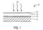
- FIG. 1The structure of a conventional Group IBIIIAVIA compound photovoltaic cell such as a Cu(In,Ga,Al)(S,Se,Te) 2 thin film solar cell is shown in FIG. 1 .
- the device 10is fabricated on a substrate 11 , such as of a sheet of glass, a sheet of metal, an insulating foil or web, or a conductive foil or web.
- the absorber film 12which comprises a material in the family of Cu(In,Ga,Al)(S,Se,Te) 2 , is grown over a conductive layer 13 or a contact layer, which is previously deposited on the substrate 11 and which acts as the ohmic contact to the device.
- Various conductive layerscomprising Mo, Ta, W, Ti, stainless steel etc. have been used in the solar cell structure of FIG. 1 . If the substrate itself is a properly selected conductive material, it is possible not to use a conductive layer 13 , since the substrate 11 may then be used as the ohmic contact to the device.
- a transparent layer 14such as a CdS, ZnO or CdS/ZnO stack is formed on the absorber film. Radiation 15 enters the device through the transparent layer 14 .
- Metallic gridsmay also be deposited over the transparent layer 14 to reduce the effective series resistance of the device.
- the preferred electrical type of the absorber film 12is p-type, and the preferred electrical type of the transparent layer 14 is n-type. However, an n-type absorber and a p-type window layer can also be utilized.
- the preferred device structure of FIG. 1is called a “substrate-type” structure.
- a “superstrate-type” structurecan also be constructed by depositing a transparent conductive layer on a transparent superstrate such as glass or transparent polymeric foil, and then depositing the Cu(In,Ga,Al)(S,Se,Te) 2 absorber film, and finally forming an ohmic contact to the device by a conductive layer. In this superstrate structure light enters the device from the superstrate side.
- heating uniformity, heating rate and sometimes cooling rateare important parameters that influence the properties of the film that is formed on the substrate. There is, therefore, a need to develop novel approaches to closely control such parameters.
- the present inventionrelates to method and apparatus for preparing thin films of materials for various applications including electronic devices such as solar cells.
- each of the method and apparatuspassing an electrical current through at least one of the base or sheet to provide controlled localized heat to the base or sheet, or to layers disposed above the base or sheet.
- the controlled localized heatis provided in combination with a process environment that can be a non-inert gas that contains an element that will become part of a compound on the base or sheet, or an inert gas that allows for the process environment to provide annealing.
- the present inventionprovides a method of forming a reacted film, the method includes providing a base; depositing on the base a precursor layer including two or more elements; and passing an electrical current through at least one of the base and the precursor layer to provide controlled localized heat to the precursor layer and cause a reaction of the two or more elements of the precursor layer to form the reacted film.
- the present inventionprovides an apparatus for forming a film on a sheet, the apparatus including a process chamber for exposing the sheet to a process environment that includes at least one constituent element; and an electrical circuit disposed with the process chamber that provides an electrical current to the sheet to cause controlled localized heat to the sheet.
- FIG. 1is a cross-sectional view of a solar cell employing a Group IBIIIAVIA absorber layer.
- FIG. 2shows a stack being heated by passing an electrical current through it.
- FIG. 2Ashows face-to-face processing in accordance with one embodiment.
- FIG. 3Ashows a stack being placed in a reactor.
- FIG. 3Bshows the stack of FIG. 3A being heated up in accordance with one embodiment while the reactor is closed.
- FIG. 4shows two temperature zones formed on a substrate using four electrical contacts.
- FIG. 5shows a film being deposited on a layer out of a solution by selectively heating the layer.
- FIG. 6shows a method of heating a substrate as a film is formed on a substrate.
- FIG. 7shows a method of heating a conductive precursor layer to form a compound layer.
- a filmis formed on a substrate comprising a conductive layer or portion.
- a currentis passed through the conductive layer or portion to heat up the conductive layer or portion and therefore the film, which is thermally coupled to it.
- the substratemay itself be a conductor, in which case there may not be a need for an additional conductive layer or portion.
- the inventionwill now be described using an example of forming thin layers of Group IBIIIAVIA semiconducting compounds. Those skilled in the art would recognize that the invention may be used to form a large variety of semiconductor, conductor or insulating layers on various substrates.
- FIG. 2shows a stack 25 made of a precursor layer 20 deposited on a base 21 .
- the precursor layer 20 of this examplemay comprise Cu, In, and Ga. It may additionally comprise a Group VIA material such as Se and/or S. These materials may be in the form of a mixture such as mixture of Cu, In, and Ga, or a mixture of Cu, In, Ga and Se, or they may be in the form of stacked sub-layer to form the precursor layer 20 .
- Sub-layersmay comprise Cu, In, Ga and Se and may be arranged in different orders to form the stacked precursor layers.
- the stacked precursor structuresinclude Cu/Ga/In, Cu/In/Ga, Cu/Ga/In/Se, CuIn/Ga/Se, Cu—Ga/In/Se, Cu—In/Ga/Se, Cu—Se/In—Se/Ga—Se, and Cu/Ga—Se/In—Se.
- the base 21may comprise a substrate 22 and a contact layer 23 .
- the substrate 22may be a conductive sheet or foil such as a stainless steel foil, a Mo foil, a Ti foil, an Al foil etc.
- the contact layermay comprise any proper material that makes good ohmic contact to Group IBIIIAVIA compound layers. These materials include Mo, Ta, W, Hf, Ru etc.
- the stack 25may be placed in an enclosure (not shown) and a current, “I”, may be passed through it by touching the stack 25 with electrodes 24 .
- a current“I”
- all the components of the stack 25i.e. the substrate 22 , the contact layer 23 and the precursor layer 20 , may be conductive. Therefore the current may pass through all these components.
- the substrate 22is typically much thicker (25-250 microns) than the rest of the layers in the stack 25 , most of the current may pass through the substrate 22 .
- the typical thickness ranges for the contact layer 23 and the precursor layer 20are, 0.1-3 microns and 0.2-2 microns, respectively.
- a current of 1-1000 Amperes (A) or largermay be passed through the stack depending on the lateral resistance of the stack which, in turn, is determined by the thickness, the width and the length of the stack 25 or the substrate 22 .
- an electrical current “I”is passed thorough the stack 25 or the substrate 22 , the temperature of the stack 25 rises and a reaction is initiated within the precursor layer 20 between Cu, In, Ga and Se. If there is no Se within the precursor layer 20 , Se or another Group VIA material, such as S and/or Te may be provided to the top surface 26 so that a Group IBIIIAVIA compound layer is formed on the contact layer 23 as a result of this reaction.
- the present inventionuses the stack and/or the base and/or the conductive substrate as a heater. Therefore, the temperature of the film forming over the substrate or the base may be controlled accurately with a fast response time. Temperature control may be achieved by attaching at least one thermocouple to the base (not shown). Temperature rise times of 10-100 C/sec may be readily obtained using this approach depending on the current density used to pass through the stack or the substrate. Such high temperature rise times are difficult to achieve in a uniform manner using standard Rapid Thermal Processing (RTP) approaches employing lamps or heater blocks. Another benefit of the present invention is increased throughput. In a regular RTP approach using heating lamps only one substrate is processed at a time. In FIG.
- RTPRapid Thermal Processing
- a bank of lampsmay be placed above the precursor layer 20 and these lamps may shine down onto the top surface 26 heating the precursor layer 20 . Therefore, it is necessary to have the top surface 26 exposed to radiation from the lamps.
- face-to-face processingmay be carried out as shown in FIG. 2A , where a first stack 27 and a second stack 28 are placed across from each other forming a gap 29 between them.
- two power suppliesas shown
- a single power supplynot shown
- Such an arrangementdoubles the throughput of the process and it forms a uniformly heated gap 29 through which inert or reactive gasses may be passed.
- first precursor layer 20 A and the second precursor layer 20 Bcomprise Cu, In, Ga and Se
- they bothwould be converted into Cu(In,Ga)Se 2 layers after the heating step which may take the temperature to a range of 200-550 C or higher.
- an inert gas, vacuum and/or Se vapormay be present in the gap 29 .
- Having a small gap of 1-5 mmalso contains the volatile Se species within the gap and increases Se utilization by keeping Se close to the precursor surface during reaction.
- both precursor layerscould be converted into Cu(In,Ga)Se 2 layers after the heating step if a Se containing gas such as H 2 Se or Se vapor is provided to the gap 29 so that the provided Se may react with the Cu, In and Ga species in the two precursor layers.
- a Se containing gassuch as H 2 Se or Se vapor is provided to the gap 29 so that the provided Se may react with the Cu, In and Ga species in the two precursor layers.
- Having a small gap of 1-5 mmcontains the volatile Se species within the gap and increases Se utilization by keeping it close to the precursor surface during reaction.
- the technique of the present inventionapplies heat directly where it is needed, i.e. directly to the film that is being formed over the substrate.
- the inventionmay also be used in a way that allows control of the cooling rate.
- FIGS. 3A and 3Bshow an example of such a case.
- FIG. 3Ashows a reactor 30 comprising an upper block 31 and lower block 32 .
- the stack 25which may be similar to the stack 25 of FIG. 2 , is placed between the upper block 31 and the lower block 32 .
- Electrodes 24 with electrical leads 35 attached to terminals of a power sourceare placed such that when the reactor 30 is closed by bringing the upper block 31 and the lower block 32 together (as shown in FIG. 3B ), they make electrical contact with the stack 25 .
- a currentmay be passed through the stack 25 via the electrodes 24 , and the stack temperature may be raised to the desired level.
- the lower block 32may be chilled or it may be kept at a pre-selected temperature.
- a gassuch as nitrogen may be brought into the lower cavity 36 via the gas inlet 33 and taken out of the cavity via the gas outlet 34 as shown in FIG. 3B .
- the electrical currentmay be cut off and a thermally conductive gas such as He may be brought into the lower cavity 36 to thermally couple the stack 25 and the lower block 32 , and rapidly cool the stack 25 down to the pre-selected temperature of the lower block 32 .
- the lower cavitymay be very shallow such as only 10-100 microns deep. Alternately, there may not be a lower cavity and the gas may just lift the stack away from the lower block 32 when passed during process. Also, if very rapid cooling is desired, vacuum may be pulled in the lower cavity to establish physical contact between the lower block 32 and the stack 25 once the heating/reaction step of the process is finished and the electrical current passing through the stack is cut off. There may be an upper cavity 37 formed between the upper block 31 and the stack 25 . The upper block 31 may or may not be heated.
- reaction gases or inert gassesmay also be brought into the upper cavity 37 .
- Se and/or S vapors or other gases containing Se and/or Smay be brought into the upper cavity 37 at the time the stack is heated up by passing the current through it.
- gasesmay participate during reaction of the precursor layer to form the compound layer.
- FIGS. 3A and 3Bmay be utilized.
- these reactorsmay be turned 90 degrees or 180 degrees yielding vertical or horizontal designs.
- the substrate 22may not be conductive but the contact layer 23 may be conductive.
- the currentmay be passed through the contact layer 23 and the contact layer 23 may be used as a thin film heater.
- face-to-face processingmay be carried out in the reactors as described in relation to FIG. 2A .
- FIG. 4schematically shows a section of a stack 25 being moved from left to right in the direction of arrow 40 .
- a first set of electrical contacts 41 A and 41 Bwhich may be sliding contacts, rollers or brushes, are provided making electrical connection to the stack 25 defining a first zone A.
- a second set of electrical contacts 42 A and 42 Bare provided making electrical connection to the stack 25 defining a second zone B.
- Power supplies P 1 and P 2may be connected to the two sets of electrical contacts as shown in the figure. Depending upon how much power is applied by the power supplies P 1 and P 2 , the temperature of the zones A and B may be pre-set or varied.
- a first current I 1may be passed through the zone A via electrical contacts 41 A and 41 B
- a second current I 2may be passed through the zone B via electrical contacts 42 A and 42 B.
- I 1 ⁇ I 2the temperature in zone B of the stack would be higher than the temperature in zone A of the stack.
- the current in zone Amay be adjusted so that the temperature in this zone goes to 200 C
- the current in zone Bmay be selected so that the temperature goes up to 500 C.
- the precursor layer of the stackmay be put through a first temperature in zone A and then a second temperature in zone B.
- the present inventionis especially suited in applications where heat needs to be applied just to the substrate or stack without dispersing it extensively to the environment of a reactor. This way desired reactions may be initiated right on the substrate or stack surface rather than on reactor walls etc.
- the conductive substrate or the stackis immersed into a reactor environment in a way to expose a face of the stack or the substrate to the reactor environment.
- the reactor environmentmay contain various chemicals, gasses, vacuum etc. that may be needed for the formation of the film on the substrate.
- Heat according to the present inventioncan be applied solely through the usage of passing the electrical current to heat the precursor layer, or a combination of using electrical current to heat the precursor layer and another heating step, either simultaneous with or after using the electrical current.
- the heat generated using the electrical currentcauses a temperature range of 200-400 C within the precursor, there will likely be the need for a further step of heating. If, however, the electrical current heats the precursor layer to a temperature range of 400-600 C, then, depending on the length of time of the heating, another heating means or another heating step may not be, and preferably is not, needed.
- fabricating a Group IBIIIAVIA solar cellssuch as a Cu(In,Ga)Se 2 solar cell involves deposition of a thin CdS layer over the Cu(In,Ga)Se 2 absorber.
- One method of depositing the CdS layeris the chemical dip method where the Cu(In,Ga)Se 2 surface is dipped in a chemical solution comprising Cd (from salts such as Cd-nitrate, Cd-sulfate, Cd-chloride etc.) and S (from sources such as thiourea), complexing agents (such as ammonia).
- Cdfrom salts such as Cd-nitrate, Cd-sulfate, Cd-chloride etc.
- Sfrom sources such as thiourea
- complexing agentssuch as ammonia
- FIG. 5shows an exemplary system 50 employing the teachings of the present invention.
- the system 50comprises a container 55 containing a solution 54 .
- the solutionmay comprise Cd and S species as mentioned before.
- the container 55may have an inlet port 56 and an outlet port 57 through which the solution 54 may be fed into and drawn out of the container 55 .
- a conductive substrate 51 coated with a layer 52 such as a Cu(In—Ga)Se 2 layeris placed in the container 55 such that a surface 53 of the layer 52 is exposed to the solution 54 .
- Electrical contacts 58are provided and connected to a power supply 59 .
- the temperature of the solutionmay be kept at a range of 10-60 C that does not allow much reaction between the Cd and S species.
- a currentmay then be passed through the electrical contacts 58 and the conductive substrate 51 , heating the conductive substrate 51 and the layer 52 to a pre-selected temperature, such as to 60-90 C.
- a micro-layer of the solution 54which is in contact with the surface 53 of the layer 52 gets heated and the Cd and S reaction is initiated within that micro-layer and on the surface 53 , selectively forming a CdS layer on the surface 53 , without wasting the bulk of the solution which may be pumped out through the outlet port 57 , filtered and fed back into the container 55 through the inlet port 56 .
- the inventionis applicable to cases where the container 55 may contain a gas rather than a liquid.
- the layer 52 on the conductive substrate 51may be a precursor layer comprising Cu, In and Ga and the container 55 may contain a gas comprising Se, such as H 2 Se gas or Se vapor.
- a reactionis initiated between the precursor layer and the gas forming a Cu(In,Ga)Se 2 compound film on the substrate 51 .
- the substrate 51may be flat, coiled or it may be a roll of metallic foil immersed in a gas comprising Se. When current is passed through the whole roll, the whole roll may be heated instantly and uniformly initiating reaction uniformly.
- heating rate of the rollwould be very non-uniform, the outside of the roll heating up first, while the core staying cooler. This would mean reaction with the reactive gas would be very non-uniform. If the whole roll is heated up by passing current through it, i.e. using the substrate roll as the heater, heating uniformity would be much better and this way large area production may be achieved without compromising the quality of the film that is formed on the substrate.
- a reactive gassuch as a gas comprising Se
- FIG. 6shows a conductive substrate 60 being coated with a film 65 on its front surface 63 .
- the substrate 60may be moving from left to right in a continuous or step-wise fashion. Electrical contacts touching the back surface 66 of the substrate complete the electrical circuit with a power supply, P, and define a zone, D. As the substrate 60 moves from left to right, the section of the substrate within the zone D gets heated to a temperature of, for example, 50-600 C if the power supply is energized.
- a material flux 62may be created by a source 61 and directed to the front surface 63 within the zone D.
- the source 61may be a sputtering target, an evaporation source, a spray gun, a doctor blade, gravure printer, ink printing head etc., depending on the deposition approach selected. Material deposits and/or reacts and/or dries on the front surface 63 forming the film 65 .
- the example aboveused a conductive substrate.
- the substratemay not be totally conductive but it may have a conductive portion or a conductive layer through which an electrical current may be passed to heat up the front surface 63 .
- the conductive substrate of the present inventionmay be a metallic foil such as an Al foil or a stainless steel foil and the film 65 may be a precursor layer comprising at least one of a Group IB material, a Group IIIA material and a Group VIA material, or it may be a Group IBIIIAVIA compound absorber layer that is deposited on the conductive substrate for the purpose of fabricating thin film solar cells.
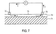
- FIG. 7shows a substrate 71 with a precursor film 70 on its surface.
- Precursor 70is conductive and may comprise elements of A, B and C (such as Cu, In and Ga).
- the substrate 71in this case may be insulating or may have high resistivity. There may be other layers such as contact layers etc between the substrate 71 and the precursor film 70 that are not shown for brevity.
- Contacts 72electrically couple a power supply, P, to the precursor layer 70 and a current, I, passes through the precursor layer 70 . Passing current heats the precursor and a reaction takes place within the precursor layer.
- Semay be provided to the top surface 73 of the precursor layer and thus a Cu(In,Ga)Se 2 compound layer may be formed through reaction of Cu, In and Ga within the precursor and Se that is provided from outside.
- the precursorcomprises all the elements required for compound formation.
- the precursormay comprise elements of A, B, C and D (such as Cu, In, Ga and Se) in the form of a mixture or in the form of thin layers.
- the A-B-C-D compoundsuch as a Cu(In,Ga)Se 2 compound.
- the compound layerforms, its conductivity gets reduced and this may be used as a self-limiting control if power supply provides a constant voltage. It should be understood that under constant voltage conditions, as a compound layer is formed from a conductive precursor layer, the resistivity may increase and therefore the current passing through the forming compound layer gets reduced, in turn reducing heating of the compound layer upon completion of the reaction.
- Group IBIIIAVIA compound layersmay be formed on spherical conductors or conductive wires which may be cylindrical in shape. This way, thin film solar cells may be obtained on cylindrical substrates or wires.
- the wiresmay be wires of stainless steel, Mo, Ti, Al etc. They may be coated with a contact layer such as Mo, W, Ta, Ru etc.
- a precursor layer comprising at least one of Group IB material, a Group IIIA material and optionally a Group VIA materialmay be deposited on the contact layer by various methods such as sputtering, evaporation, electrodeposition etc. Electrodeposition is especially attractive because of high material utilization. Precursors comprising Cu, In and Ga may be electrodeposited, for example, on contact layers at high efficiency. Once formed, the precursor layers are reacted in presence of Group VIA materials to form Group IBIIIAVIA layers such as Cu(In,Ga)Se 2 layers on the wires.
- solar cellsmay be fabricated on the compound layers of the present invention using materials and methods well known in the field. For example a thin ( ⁇ 0.1 microns) CdS layer may be deposited on the surface of the compound layer using the chemical dip method. A transparent window of ZnO may be deposited over the CdS layer using MOCVD or sputtering techniques. A metallic finger pattern is optionally deposited over the ZnO to complete the solar cell.
- a thin ( ⁇ 0.1 microns) CdS layermay be deposited on the surface of the compound layer using the chemical dip method.
- a transparent window of ZnOmay be deposited over the CdS layer using MOCVD or sputtering techniques.
- a metallic finger patternis optionally deposited over the ZnO to complete the solar cell.
Landscapes
- Chemical & Material Sciences (AREA)
- Engineering & Computer Science (AREA)
- Metallurgy (AREA)
- Chemical Kinetics & Catalysis (AREA)
- Organic Chemistry (AREA)
- Mechanical Engineering (AREA)
- Materials Engineering (AREA)
- Microelectronics & Electronic Packaging (AREA)
- Condensed Matter Physics & Semiconductors (AREA)
- Power Engineering (AREA)
- General Physics & Mathematics (AREA)
- Computer Hardware Design (AREA)
- Physics & Mathematics (AREA)
- Manufacturing & Machinery (AREA)
- Photovoltaic Devices (AREA)
- Recrystallisation Techniques (AREA)
Abstract
Description
Claims (13)
Priority Applications (5)
| Application Number | Priority Date | Filing Date | Title |
|---|---|---|---|
| US11/735,430US7585547B2 (en) | 2006-04-13 | 2007-04-13 | Method and apparatus to form thin layers of materials on a base |
| US12/037,076US7541067B2 (en) | 2006-04-13 | 2008-02-25 | Method and apparatus for continuous processing of buffer layers for group IBIIIAVIA solar cells |
| US12/463,303US8225742B2 (en) | 2006-04-13 | 2009-05-08 | Apparatus for continuous processing of buffer layers for group IBIIIAVIA solar cells |
| US12/464,673US7923281B2 (en) | 2006-04-13 | 2009-05-12 | Roll-to-roll processing method and tools for electroless deposition of thin layers |
| US12/478,561US8156891B2 (en) | 2006-04-13 | 2009-06-04 | Apparatus for simultaneous roll-to-roll wet processing of two workpieces disposed within a single chamber |
Applications Claiming Priority (2)
| Application Number | Priority Date | Filing Date | Title |
|---|---|---|---|
| US74482706P | 2006-04-13 | 2006-04-13 | |
| US11/735,430US7585547B2 (en) | 2006-04-13 | 2007-04-13 | Method and apparatus to form thin layers of materials on a base |
Related Parent Applications (1)
| Application Number | Title | Priority Date | Filing Date |
|---|---|---|---|
| US12/037,076Continuation-In-PartUS7541067B2 (en) | 2006-04-13 | 2008-02-25 | Method and apparatus for continuous processing of buffer layers for group IBIIIAVIA solar cells |
Related Child Applications (2)
| Application Number | Title | Priority Date | Filing Date |
|---|---|---|---|
| US12/037,076Continuation-In-PartUS7541067B2 (en) | 2006-04-13 | 2008-02-25 | Method and apparatus for continuous processing of buffer layers for group IBIIIAVIA solar cells |
| US12/464,673Continuation-In-PartUS7923281B2 (en) | 2006-04-13 | 2009-05-12 | Roll-to-roll processing method and tools for electroless deposition of thin layers |
Publications (2)
| Publication Number | Publication Date |
|---|---|
| US20070243657A1 US20070243657A1 (en) | 2007-10-18 |
| US7585547B2true US7585547B2 (en) | 2009-09-08 |
Family
ID=38610416
Family Applications (1)
| Application Number | Title | Priority Date | Filing Date |
|---|---|---|---|
| US11/735,430Expired - Fee RelatedUS7585547B2 (en) | 2006-04-13 | 2007-04-13 | Method and apparatus to form thin layers of materials on a base |
Country Status (2)
| Country | Link |
|---|---|
| US (1) | US7585547B2 (en) |
| WO (1) | WO2007121383A2 (en) |
Cited By (7)
| Publication number | Priority date | Publication date | Assignee | Title |
|---|---|---|---|---|
| US20080057616A1 (en)* | 2006-06-12 | 2008-03-06 | Robinson Matthew R | Bandgap grading in thin-film devices via solid group iiia particles |
| US20090117684A1 (en)* | 2007-10-26 | 2009-05-07 | Basol Bulent M | Method and apparatus for forming copper indium gallium chalcogenide layers |
| US20090246908A1 (en)* | 2006-04-13 | 2009-10-01 | Solopower, Inc. | Roll-to-roll processing method and tools for electroless deposition of thin layers |
| US20100291727A1 (en)* | 2009-05-12 | 2010-11-18 | Solopower, Inc. | Roll-to-roll processing method and tools for electroless deposition of thin layers |
| US8418418B2 (en) | 2009-04-29 | 2013-04-16 | 3Form, Inc. | Architectural panels with organic photovoltaic interlayers and methods of forming the same |
| US8539907B2 (en) | 2010-11-30 | 2013-09-24 | Industrial Technology Research Institute | Apparatus for chemical bath deposition between two covers, wherein a cover is a substrate |
| EP4340047A4 (en)* | 2021-05-11 | 2025-04-30 | Mecaroenergy Co. Ltd. | METHOD FOR PRODUCING A CIGS LIGHT ABSORPTION LAYER FOR A SOLAR CELL BY CHEMICAL VAPOR DEPOSITION |
Families Citing this family (31)
| Publication number | Priority date | Publication date | Assignee | Title |
|---|---|---|---|---|
| US8071179B2 (en) | 2007-06-29 | 2011-12-06 | Stion Corporation | Methods for infusing one or more materials into nano-voids if nanoporous or nanostructured materials |
| EP2206141A4 (en)* | 2007-10-17 | 2012-10-10 | Yann Roussillon | ARRANGEMENT FOR IMPROVED DEPOSITION OF A SOLUTION |
| US20100087015A1 (en) | 2008-03-05 | 2010-04-08 | Global Solar Energy, Inc. | Feedback for buffer layer deposition |
| DE112009000532T5 (en)* | 2008-03-05 | 2011-03-10 | Global Solar Energy, Inc., Tuscon | Heater for buffer layer application |
| DE212009000031U1 (en)* | 2008-03-05 | 2010-11-04 | Global Solar Energy, Inc., Tuscon | Device for applying a thin-layer buffer layer to a flexible carrier |
| US8062922B2 (en)* | 2008-03-05 | 2011-11-22 | Global Solar Energy, Inc. | Buffer layer deposition for thin-film solar cells |
| US9252318B2 (en) | 2008-03-05 | 2016-02-02 | Hanergy Hi-Tech Power (Hk) Limited | Solution containment during buffer layer deposition |
| US8383450B2 (en)* | 2008-09-30 | 2013-02-26 | Stion Corporation | Large scale chemical bath system and method for cadmium sulfide processing of thin film photovoltaic materials |
| US7947524B2 (en) | 2008-09-30 | 2011-05-24 | Stion Corporation | Humidity control and method for thin film photovoltaic materials |
| US8232134B2 (en)* | 2008-09-30 | 2012-07-31 | Stion Corporation | Rapid thermal method and device for thin film tandem cell |
| US20110018103A1 (en)* | 2008-10-02 | 2011-01-27 | Stion Corporation | System and method for transferring substrates in large scale processing of cigs and/or cis devices |
| US8030188B2 (en)* | 2008-12-05 | 2011-10-04 | Electronics And Telecommunications Research Institute | Methods of forming a compound semiconductor device including a diffusion region |
| US8241943B1 (en) | 2009-05-08 | 2012-08-14 | Stion Corporation | Sodium doping method and system for shaped CIGS/CIS based thin film solar cells |
| US8372684B1 (en) | 2009-05-14 | 2013-02-12 | Stion Corporation | Method and system for selenization in fabricating CIGS/CIS solar cells |
| US8507786B1 (en) | 2009-06-27 | 2013-08-13 | Stion Corporation | Manufacturing method for patterning CIGS/CIS solar cells |
| US8398772B1 (en) | 2009-08-18 | 2013-03-19 | Stion Corporation | Method and structure for processing thin film PV cells with improved temperature uniformity |
| JP5462558B2 (en)* | 2009-09-08 | 2014-04-02 | 東京応化工業株式会社 | Coating apparatus and coating method |
| JP5639816B2 (en)* | 2009-09-08 | 2014-12-10 | 東京応化工業株式会社 | Coating method and coating apparatus |
| JP5439097B2 (en)* | 2009-09-08 | 2014-03-12 | 東京応化工業株式会社 | Coating apparatus and coating method |
| JP5719546B2 (en)* | 2009-09-08 | 2015-05-20 | 東京応化工業株式会社 | Coating apparatus and coating method |
| TW201124544A (en)* | 2009-11-24 | 2011-07-16 | Applied Quantum Technology Llc | Chalcogenide absorber layers for photovoltaic applications and methods of manufacturing the same |
| US8859880B2 (en)* | 2010-01-22 | 2014-10-14 | Stion Corporation | Method and structure for tiling industrial thin-film solar devices |
| US8142521B2 (en)* | 2010-03-29 | 2012-03-27 | Stion Corporation | Large scale MOCVD system for thin film photovoltaic devices |
| US9096930B2 (en) | 2010-03-29 | 2015-08-04 | Stion Corporation | Apparatus for manufacturing thin film photovoltaic devices |
| US8461061B2 (en) | 2010-07-23 | 2013-06-11 | Stion Corporation | Quartz boat method and apparatus for thin film thermal treatment |
| US8906732B2 (en)* | 2010-10-01 | 2014-12-09 | Stion Corporation | Method and device for cadmium-free solar cells |
| JP5862080B2 (en)* | 2011-07-06 | 2016-02-16 | ソニー株式会社 | Graphene production method and graphene production apparatus |
| JP2015061062A (en)* | 2013-09-20 | 2015-03-30 | 株式会社東芝 | Photoelectric conversion element manufacturing method |
| TWI720181B (en)* | 2016-05-30 | 2021-03-01 | 日商新力股份有限公司 | Thin film manufacturing method, thin film manufacturing device, manufacturing method of photoelectric conversion element, manufacturing method of logic circuit, manufacturing method of light-emitting element, and manufacturing method of dimming element |
| CN109402575A (en)* | 2018-12-27 | 2019-03-01 | 北京铂阳顶荣光伏科技有限公司 | Pedestal and evaporated device |
| CN112531078B (en)* | 2020-12-18 | 2022-05-20 | 尚越光电科技股份有限公司 | Defect passivation method for solving problem of light attenuation of copper indium gallium selenide solar cell |
Citations (10)
| Publication number | Priority date | Publication date | Assignee | Title |
|---|---|---|---|---|
| US4798660A (en) | 1985-07-16 | 1989-01-17 | Atlantic Richfield Company | Method for forming Cu In Se2 films |
| US4915745A (en)* | 1988-09-22 | 1990-04-10 | Atlantic Richfield Company | Thin film solar cell and method of making |
| US5410796A (en) | 1993-10-06 | 1995-05-02 | Technical Research Associates, Inc. | Copper/copper alloy and graphite fiber composite and method |
| US5476811A (en)* | 1988-11-28 | 1995-12-19 | Fujitsu Limited | Method of growing epitaxial layers |
| US5997956A (en) | 1995-08-04 | 1999-12-07 | Microcoating Technologies | Chemical vapor deposition and powder formation using thermal spray with near supercritical and supercritical fluid solutions |
| US6048442A (en) | 1996-10-25 | 2000-04-11 | Showa Shell Sekiyu K.K. | Method for producing thin-film solar cell and equipment for producing the same |
| US20010006734A1 (en) | 1999-07-07 | 2001-07-05 | Hulya Demiryont | Heat treatable coated glass |
| US6537845B1 (en)* | 2001-08-30 | 2003-03-25 | Mccandless Brian E. | Chemical surface deposition of ultra-thin semiconductors |
| US6547876B2 (en)* | 2001-02-07 | 2003-04-15 | Emcore Corporation | Apparatus for growing epitaxial layers on wafers by chemical vapor deposition |
| US6923625B2 (en) | 2002-01-07 | 2005-08-02 | Integrated Sensing Systems, Inc. | Method of forming a reactive material and article formed thereby |
Family Cites Families (87)
| Publication number | Priority date | Publication date | Assignee | Title |
|---|---|---|---|---|
| US3104448A (en)* | 1961-09-21 | 1963-09-24 | Morrow | Mortician's body cavity injector |
| US3529580A (en)* | 1968-10-23 | 1970-09-22 | Foster Wheeler Corp | Start-up system |
| US4021920A (en)* | 1973-06-18 | 1977-05-10 | Horst Kirschner | Drilling or milling apparatus for the working of live bone, particularly for dentistry |
| US3835860A (en)* | 1973-06-21 | 1974-09-17 | H Garretson | Surgical bone punch |
| US4099518A (en)* | 1976-05-10 | 1978-07-11 | Baylis Shelby M | Biopsy apparatus |
| SE434332B (en)* | 1983-03-23 | 1984-07-23 | Jan Ingemar Neslund | CELL SAMPLING DEVICE |
| GB8424436D0 (en)* | 1984-09-27 | 1984-10-31 | Pratt Int Ltd Burnerd | Surgical appliance |
| GB8527646D0 (en)* | 1985-11-08 | 1985-12-11 | Cox J A | Devices for sampling drainage |
| GB8627808D0 (en)* | 1986-11-20 | 1986-12-17 | Cox J A | Sampling liquids from human/animal body |
| US4944677A (en)* | 1987-06-29 | 1990-07-31 | Raymond Joseph Alexandre | Intraosseus dental anesthesia apparatus and method |
| US5529580A (en)* | 1987-10-30 | 1996-06-25 | Olympus Optical Co., Ltd. | Surgical resecting tool |
| US4940459A (en)* | 1988-10-12 | 1990-07-10 | Mallinckrodt, Inc. | Inflation device for balloon catheter |
| US4919146A (en)* | 1988-10-25 | 1990-04-24 | Medrad, Inc. | Biopsy device |
| US4986279A (en)* | 1989-03-01 | 1991-01-22 | National-Standard Company | Localization needle assembly with reinforced needle assembly |
| US5400798A (en)* | 1989-03-29 | 1995-03-28 | Baran; Gregory W. | Automated biopsy instrument |
| US5025797A (en)* | 1989-03-29 | 1991-06-25 | Baran Gregory W | Automated biopsy instrument |
| US4921013A (en)* | 1989-08-21 | 1990-05-01 | Aeroquip Corporation | Coupling adapter |
| DE4118732A1 (en)* | 1991-06-07 | 1992-12-10 | Joka Kathetertechnik Gmbh | HOSE CLAMP FOR MEDICAL PURPOSES |
| US5332398A (en)* | 1992-02-01 | 1994-07-26 | Board Of Regents, The University Of Texas System | Intramedullary catheter |
| US5290276A (en)* | 1992-02-06 | 1994-03-01 | Sewell Jr Frank | Rotatable laparoscopic puncturing instrument |
| US5333790A (en)* | 1992-04-20 | 1994-08-02 | Christopher Gilman O | Quick disconnect nozzle apparatus |
| US5315737A (en)* | 1992-06-29 | 1994-05-31 | Serge Ouimet | Worm drive clamp with band guide channels |
| US5307924A (en)* | 1993-03-26 | 1994-05-03 | Abbott Laboratories | Packaging for T-shaped tension devices |
| US5526821A (en)* | 1993-06-03 | 1996-06-18 | Medical Biopsy, Inc. | Biopsy needle with sample retaining means |
| US6716216B1 (en)* | 1998-08-14 | 2004-04-06 | Kyphon Inc. | Systems and methods for treating vertebral bodies |
| US5649547A (en)* | 1994-03-24 | 1997-07-22 | Biopsys Medical, Inc. | Methods and devices for automated biopsy and collection of soft tissue |
| GB9417399D0 (en)* | 1994-08-30 | 1994-10-19 | Scherer Corp R P | Ocular treatment device |
| US6468248B2 (en)* | 1995-06-06 | 2002-10-22 | David Gibbs | Device for targeted, catherized delivery of medications |
| US6905486B2 (en)* | 1995-06-06 | 2005-06-14 | David Gibbs | Device for targeted, catheterized delivery of medications |
| US5769086A (en)* | 1995-12-06 | 1998-06-23 | Biopsys Medical, Inc. | Control system and method for automated biopsy device |
| US6749576B2 (en)* | 1996-01-26 | 2004-06-15 | Allegiance Corporation | Biopsy device with adjustable sampling |
| US5916229A (en)* | 1996-02-07 | 1999-06-29 | Evans; Donald | Rotating needle biopsy device and method |
| US5800389A (en)* | 1996-02-09 | 1998-09-01 | Emx, Inc. | Biopsy device |
| FR2744629B1 (en)* | 1996-02-13 | 1998-05-22 | Advanced Technical Fabrication | HIP PROSTHESIS INSTRUMENTATION |
| US5733262A (en)* | 1996-04-18 | 1998-03-31 | Paul; Kamaljit S. | Blood vessel cannulation device |
| US5724873A (en)* | 1996-07-12 | 1998-03-10 | Hillinger; George | Composite magnetic-field screwdriver |
| US6027458A (en)* | 1996-12-23 | 2000-02-22 | Janssens; Jacques Phillibert | Device for taking a tissue sample |
| US6716192B1 (en)* | 1997-09-30 | 2004-04-06 | Charles F. Schroeder | Medical needle having a visibly marked tip |
| ES2196292T3 (en)* | 1997-10-06 | 2003-12-16 | Pirelli | REINFORCEMENT FABRIC FOR AN ARTICLE MANUFACTURED FROM ELASTOMERIC MATERIAL AND CORRESPONDING ARTICLE UNDERSTANDED SUCH FABRIC. |
| US6033411A (en)* | 1997-10-14 | 2000-03-07 | Parallax Medical Inc. | Precision depth guided instruments for use in vertebroplasty |
| US5911701A (en)* | 1998-01-29 | 1999-06-15 | Sdgi Holidings, Inc. | Surgical cutting instrument |
| DE19806693A1 (en)* | 1998-02-18 | 1999-08-19 | Daum Gmbh | Telescopically working needle and tube system for removal of tumor |
| US6193673B1 (en)* | 1998-02-20 | 2001-02-27 | United States Surgical Corporation | Biopsy instrument driver apparatus |
| US6183442B1 (en)* | 1998-03-02 | 2001-02-06 | Board Of Regents Of The University Of Texas System | Tissue penetrating device and methods for using same |
| CA2287087C (en)* | 1998-10-23 | 2007-12-04 | Ethicon Endo-Surgery, Inc. | Surgical device for the collection of soft tissue |
| US20010047183A1 (en)* | 2000-04-05 | 2001-11-29 | Salvatore Privitera | Surgical device for the collection of soft tissue |
| AU3306500A (en)* | 1999-03-19 | 2000-10-09 | Paul Cervi | Biopsy needle |
| US6402701B1 (en)* | 1999-03-23 | 2002-06-11 | Fna Concepts, Llc | Biopsy needle instrument |
| US6086544A (en)* | 1999-03-31 | 2000-07-11 | Ethicon Endo-Surgery, Inc. | Control apparatus for an automated surgical biopsy device |
| US6547561B2 (en)* | 1999-06-09 | 2003-04-15 | Tulsa Dental Products Inc. | Disposable anesthesia delivery system with shortened outer sleeve and inner hollow drill |
| US6500180B1 (en)* | 1999-10-20 | 2002-12-31 | Sdgi Holdings, Inc. | Methods and instrumentation for distraction of a disc space |
| US6716215B1 (en)* | 1999-10-29 | 2004-04-06 | Image-Guided Neurologics | Cranial drill with sterile barrier |
| US6585622B1 (en)* | 1999-12-03 | 2003-07-01 | Nike, Inc. | Interactive use an athletic performance monitoring and reward method, system, and computer program product |
| US6428487B1 (en)* | 1999-12-17 | 2002-08-06 | Ethicon Endo-Surgery, Inc. | Surgical biopsy system with remote control for selecting an operational mode |
| US6702761B1 (en)* | 2000-03-06 | 2004-03-09 | Fonar Corporation | Vibration assisted needle device |
| US7201722B2 (en)* | 2000-04-18 | 2007-04-10 | Allegiance Corporation | Bone biopsy instrument having improved sample retention |
| EP1175866B1 (en)* | 2000-07-29 | 2006-12-06 | Worldwide Medical Technologies | Bone marrow extraction tool |
| US6730044B2 (en)* | 2000-10-13 | 2004-05-04 | Ethicon Endo-Surgery, Inc. | Firing mechanism for use in a surgical biopsy device |
| US6656133B2 (en)* | 2000-10-13 | 2003-12-02 | Ethicon Endo-Surgery, Inc. | Transmission assembly for a surgical biopsy device |
| US6540694B1 (en)* | 2000-10-16 | 2003-04-01 | Sanarus Medical, Inc. | Device for biopsy tumors |
| US6527736B1 (en)* | 2000-10-23 | 2003-03-04 | Grieshaber & Co. Ag Schaffhausen | Device for use in ophthalmologic procedures |
| AU2002245125A1 (en)* | 2000-11-06 | 2002-07-08 | Francis C. Classe | Biopsy and coagulant device |
| WO2002069808A2 (en)* | 2000-11-06 | 2002-09-12 | Suros Surgical Systems, Inc. | Biopsy apparatus |
| US6758824B1 (en)* | 2000-11-06 | 2004-07-06 | Suros Surgical Systems, Inc. | Biopsy apparatus |
| CA2429572A1 (en)* | 2000-11-24 | 2002-07-18 | Ckm Diagnostics, Inc. | Nerve stimulator output control needle with depth determination capability and method of use |
| EP1339326B1 (en)* | 2000-11-27 | 2013-03-06 | Covidien LP | Tissue sampling and removal apparatus |
| US6419490B1 (en)* | 2001-01-30 | 2002-07-16 | Arthur Kitchings Weathers, Jr. | Grooved intraosseous dental drill bit |
| BE1013974A3 (en)* | 2001-02-16 | 2003-01-14 | Janssens Jacques Phillibert | Device for taking a tissue language. |
| US7544196B2 (en)* | 2001-02-20 | 2009-06-09 | Orthovita, Inc. | System and kit for delivery of restorative materials |
| US6595911B2 (en)* | 2001-04-03 | 2003-07-22 | Lovuolo Michael | Method and device for anchor implantation and support of bodily structures |
| US6554809B2 (en)* | 2001-08-02 | 2003-04-29 | Teodulo Aves | Epidural catheter needle |
| US6849051B2 (en)* | 2001-08-03 | 2005-02-01 | Stemsource Llc | Devices and methods for extraction of bone marrow |
| DE60112591T2 (en)* | 2001-11-23 | 2006-05-18 | Nucletron B.V. | Automatic image-controlled device for introducing a cannula into a human or animal body for radiotherapy in this body |
| US20030125639A1 (en)* | 2002-01-02 | 2003-07-03 | Fisher John S. | Biopsy needle having rotating core for shearing tissue |
| US6887209B2 (en)* | 2002-01-25 | 2005-05-03 | Advanced Medical Optics | Pulsed vacuum and/or flow method and apparatus for tissue removal |
| WO2003079907A1 (en)* | 2002-03-20 | 2003-10-02 | Board Of Regents, The University Of Texas System | Biopsy needle |
| US7326203B2 (en)* | 2002-09-30 | 2008-02-05 | Depuy Acromed, Inc. | Device for advancing a functional element through tissue |
| US7740597B2 (en)* | 2002-12-11 | 2010-06-22 | Ethicon Endo-Surgery, Inc. | Biopsy device with sample tube |
| US7229419B2 (en)* | 2003-02-11 | 2007-06-12 | Promex/U.S. Biosy Llc | Single-handed biopsy system |
| JP4754474B2 (en)* | 2003-02-25 | 2011-08-24 | エシコン・エンド−サージェリィ・インコーポレイテッド | Biopsy device with variable speed cutter |
| WO2005112800A2 (en)* | 2004-05-17 | 2005-12-01 | Tiax Llc | Intraosseous infusion device |
| US20060074345A1 (en)* | 2004-09-29 | 2006-04-06 | Hibner John A | Biopsy apparatus and method |
| US20060079774A1 (en)* | 2004-10-08 | 2006-04-13 | Wendell Anderson | Microwave biopsy probe |
| US7329227B2 (en)* | 2004-10-21 | 2008-02-12 | Inter-V-Manan | Forward-fired automatic tissue sampling apparatus with safety lock |
| US20060122535A1 (en)* | 2004-12-08 | 2006-06-08 | Wolfgang Daum | Method and device to obtain percutaneous tissue samples |
| US20060144548A1 (en)* | 2004-12-30 | 2006-07-06 | Beckman Andrew T | Method of manufacturing a needle assembly for use with a biopsy device |
| US20060189940A1 (en)* | 2005-02-24 | 2006-08-24 | Kirsch Andrew J | Implant positioning system and method |
- 2007
- 2007-04-13USUS11/735,430patent/US7585547B2/ennot_activeExpired - Fee Related
- 2007-04-13WOPCT/US2007/066672patent/WO2007121383A2/enactiveApplication Filing
Patent Citations (12)
| Publication number | Priority date | Publication date | Assignee | Title |
|---|---|---|---|---|
| US4798660A (en) | 1985-07-16 | 1989-01-17 | Atlantic Richfield Company | Method for forming Cu In Se2 films |
| US4915745A (en)* | 1988-09-22 | 1990-04-10 | Atlantic Richfield Company | Thin film solar cell and method of making |
| US4915745B1 (en)* | 1988-09-22 | 1992-04-07 | A Pollock Gary | |
| US5476811A (en)* | 1988-11-28 | 1995-12-19 | Fujitsu Limited | Method of growing epitaxial layers |
| US5410796A (en) | 1993-10-06 | 1995-05-02 | Technical Research Associates, Inc. | Copper/copper alloy and graphite fiber composite and method |
| US5997956A (en) | 1995-08-04 | 1999-12-07 | Microcoating Technologies | Chemical vapor deposition and powder formation using thermal spray with near supercritical and supercritical fluid solutions |
| US6048442A (en) | 1996-10-25 | 2000-04-11 | Showa Shell Sekiyu K.K. | Method for producing thin-film solar cell and equipment for producing the same |
| US6092669A (en) | 1996-10-25 | 2000-07-25 | Showa Shell Sekiyu K.K. | Equipment for producing thin-film solar cell |
| US20010006734A1 (en) | 1999-07-07 | 2001-07-05 | Hulya Demiryont | Heat treatable coated glass |
| US6547876B2 (en)* | 2001-02-07 | 2003-04-15 | Emcore Corporation | Apparatus for growing epitaxial layers on wafers by chemical vapor deposition |
| US6537845B1 (en)* | 2001-08-30 | 2003-03-25 | Mccandless Brian E. | Chemical surface deposition of ultra-thin semiconductors |
| US6923625B2 (en) | 2002-01-07 | 2005-08-02 | Integrated Sensing Systems, Inc. | Method of forming a reactive material and article formed thereby |
Non-Patent Citations (3)
| Title |
|---|
| International Search Report issued Aug. 13, 2008 in PCT/US2007/66672. |
| Malinowska et al. Cadmium Recovery and Recycling from Chemical Bath Deposition of CdS Thin Layers, Progress in Photovoltaics: Research and applications, 2002, 10: pp. 215-228.* |
| Voss C., et al. "Growth kinetics of thin-film cadmium sulfide by ammonia-thiourea based CBD" J. of the Electrochemical Society, 151 (10); pp. C655-C660 (2204. |
Cited By (13)
| Publication number | Priority date | Publication date | Assignee | Title |
|---|---|---|---|---|
| US20090246908A1 (en)* | 2006-04-13 | 2009-10-01 | Solopower, Inc. | Roll-to-roll processing method and tools for electroless deposition of thin layers |
| US7923281B2 (en)* | 2006-04-13 | 2011-04-12 | Solopower, Inc. | Roll-to-roll processing method and tools for electroless deposition of thin layers |
| US20080057616A1 (en)* | 2006-06-12 | 2008-03-06 | Robinson Matthew R | Bandgap grading in thin-film devices via solid group iiia particles |
| US20110114182A1 (en)* | 2006-06-12 | 2011-05-19 | Robinson Matthew R | Thin-film devices formed from solid group iiia particles |
| US8372685B2 (en) | 2006-06-12 | 2013-02-12 | Nanosolar, Inc. | Bandgap grading in thin-film devices via solid group IIIA particles |
| US20090117684A1 (en)* | 2007-10-26 | 2009-05-07 | Basol Bulent M | Method and apparatus for forming copper indium gallium chalcogenide layers |
| US8258001B2 (en)* | 2007-10-26 | 2012-09-04 | Solopower, Inc. | Method and apparatus for forming copper indium gallium chalcogenide layers |
| US9076731B2 (en) | 2009-04-29 | 2015-07-07 | 3Form, Llc | Architectural panels with organic photovoltaic interlayers and methods of forming the same |
| US8418418B2 (en) | 2009-04-29 | 2013-04-16 | 3Form, Inc. | Architectural panels with organic photovoltaic interlayers and methods of forming the same |
| US20100291727A1 (en)* | 2009-05-12 | 2010-11-18 | Solopower, Inc. | Roll-to-roll processing method and tools for electroless deposition of thin layers |
| US8497152B2 (en) | 2009-05-12 | 2013-07-30 | Solopower, Inc. | Roll-to-roll processing method and tools for electroless deposition of thin layers |
| US8539907B2 (en) | 2010-11-30 | 2013-09-24 | Industrial Technology Research Institute | Apparatus for chemical bath deposition between two covers, wherein a cover is a substrate |
| EP4340047A4 (en)* | 2021-05-11 | 2025-04-30 | Mecaroenergy Co. Ltd. | METHOD FOR PRODUCING A CIGS LIGHT ABSORPTION LAYER FOR A SOLAR CELL BY CHEMICAL VAPOR DEPOSITION |
Also Published As
| Publication number | Publication date |
|---|---|
| WO2007121383A2 (en) | 2007-10-25 |
| WO2007121383A3 (en) | 2008-11-27 |
| US20070243657A1 (en) | 2007-10-18 |
Similar Documents
| Publication | Publication Date | Title |
|---|---|---|
| US7585547B2 (en) | Method and apparatus to form thin layers of materials on a base | |
| CN101578386B (en) | Method and apparatus for converting precursor layers into photovoltaic absorbers | |
| EP2013382B1 (en) | Composition control for roll-to- roll processed photovoltaic films | |
| US8192594B2 (en) | Technique and apparatus for depositing thin layers of semiconductors for solar cell fabrication | |
| US7736913B2 (en) | Composition control for photovoltaic thin film manufacturing | |
| US8066863B2 (en) | Electrodeposition technique and apparatus to form selenium containing layers | |
| US8163090B2 (en) | Methods structures and apparatus to provide group VIA and IA materials for solar cell absorber formation | |
| US20080175993A1 (en) | Reel-to-reel reaction of a precursor film to form solar cell absorber | |
| JP2013500400A (en) | Method for producing copper-containing three-component and four-component chalcogenide thin films | |
| US8921151B2 (en) | Back-contact for thin film solar cells optimized for light trapping for ultrathin absorbers | |
| EP2319952B1 (en) | Method and system for depositing multiple materials on a substrate | |
| TW201123470A (en) | Thermal management and method for large scale processing of CIS and/or CIGS based thin films overlying glass substrates | |
| TW201027771A (en) | Photovoltaic devices including copper indium gallium selenide | |
| CN211595770U (en) | Vacuum coating machine and heating device thereof | |
| WO2005081789A2 (en) | Formation of CIGS Absorber Layer by Atomic Layer Deposition | |
| JPH11121778A (en) | Manufacture of compound semiconductor film and solar cell | |
| WO2011135420A1 (en) | Process for the production of a compound semiconductor layer | |
| JPH10290016A (en) | Formation of cadmium sulfide and solar cell using thereof |
Legal Events
| Date | Code | Title | Description |
|---|---|---|---|
| AS | Assignment | Owner name:SOLOPOWER, INC., CALIFORNIA Free format text:ASSIGNMENT OF ASSIGNORS INTEREST;ASSIGNORS:BASOL, BULENT M.;ERDEMLI, SERKAN;REEL/FRAME:019508/0748 Effective date:20070614 | |
| AS | Assignment | Owner name:BRIDGE BANK, NATIONAL ASSOCIATION,CALIFORNIA Free format text:SECURITY AGREEMENT;ASSIGNOR:SOLOPOWER, INC.;REEL/FRAME:023900/0925 Effective date:20100203 Owner name:BRIDGE BANK, NATIONAL ASSOCIATION, CALIFORNIA Free format text:SECURITY AGREEMENT;ASSIGNOR:SOLOPOWER, INC.;REEL/FRAME:023900/0925 Effective date:20100203 | |
| AS | Assignment | Owner name:DEUTSCHE BANK TRUST COMPANY AMERICAS, AS COLLATERA Free format text:SECURITY AGREEMENT;ASSIGNOR:SOLOPOWER, INC.;REEL/FRAME:023905/0479 Effective date:20100204 | |
| AS | Assignment | Owner name:DEUTSCHE BANK TRUST COMPANY AMERICAS, NEW YORK Free format text:SECURITY AGREEMENT;ASSIGNOR:SOLOPOWER, INC.;REEL/FRAME:025671/0756 Effective date:20100204 | |
| AS | Assignment | Owner name:SOLOPOWER, INC., CALIFORNIA Free format text:RELEASE BY SECURED PARTY;ASSIGNOR:DEUTSCHE BANK TRUST COMPANY AMERICAS;REEL/FRAME:025897/0374 Effective date:20110119 | |
| REMI | Maintenance fee reminder mailed | ||
| AS | Assignment | Owner name:SPOWER, LLC, OREGON Free format text:MERGER;ASSIGNOR:SOLOPOWER, INC.;REEL/FRAME:030982/0818 Effective date:20130730 | |
| AS | Assignment | Owner name:SOLOPOWER SYSTEMS, INC., OREGON Free format text:ASSIGNMENT OF ASSIGNORS INTEREST;ASSIGNOR:SPOWER, LLC;REEL/FRAME:031003/0067 Effective date:20130809 | |
| LAPS | Lapse for failure to pay maintenance fees | ||
| STCH | Information on status: patent discontinuation | Free format text:PATENT EXPIRED DUE TO NONPAYMENT OF MAINTENANCE FEES UNDER 37 CFR 1.362 | |
| FP | Lapsed due to failure to pay maintenance fee | Effective date:20130908 |