US7584942B2 - Ampoules for producing a reaction gas and systems for depositing materials onto microfeature workpieces in reaction chambers - Google Patents
Ampoules for producing a reaction gas and systems for depositing materials onto microfeature workpieces in reaction chambersDownload PDFInfo
- Publication number
- US7584942B2 US7584942B2US10/814,573US81457304AUS7584942B2US 7584942 B2US7584942 B2US 7584942B2US 81457304 AUS81457304 AUS 81457304AUS 7584942 B2US7584942 B2US 7584942B2
- Authority
- US
- United States
- Prior art keywords
- precursor
- carrier gas
- conduit
- headspace
- ampoule
- Prior art date
- Legal status (The legal status is an assumption and is not a legal conclusion. Google has not performed a legal analysis and makes no representation as to the accuracy of the status listed.)
- Expired - Fee Related, expires
Links
Images


Classifications
- C—CHEMISTRY; METALLURGY
- C23—COATING METALLIC MATERIAL; COATING MATERIAL WITH METALLIC MATERIAL; CHEMICAL SURFACE TREATMENT; DIFFUSION TREATMENT OF METALLIC MATERIAL; COATING BY VACUUM EVAPORATION, BY SPUTTERING, BY ION IMPLANTATION OR BY CHEMICAL VAPOUR DEPOSITION, IN GENERAL; INHIBITING CORROSION OF METALLIC MATERIAL OR INCRUSTATION IN GENERAL
- C23C—COATING METALLIC MATERIAL; COATING MATERIAL WITH METALLIC MATERIAL; SURFACE TREATMENT OF METALLIC MATERIAL BY DIFFUSION INTO THE SURFACE, BY CHEMICAL CONVERSION OR SUBSTITUTION; COATING BY VACUUM EVAPORATION, BY SPUTTERING, BY ION IMPLANTATION OR BY CHEMICAL VAPOUR DEPOSITION, IN GENERAL
- C23C16/00—Chemical coating by decomposition of gaseous compounds, without leaving reaction products of surface material in the coating, i.e. chemical vapour deposition [CVD] processes
- C23C16/44—Chemical coating by decomposition of gaseous compounds, without leaving reaction products of surface material in the coating, i.e. chemical vapour deposition [CVD] processes characterised by the method of coating
- C23C16/448—Chemical coating by decomposition of gaseous compounds, without leaving reaction products of surface material in the coating, i.e. chemical vapour deposition [CVD] processes characterised by the method of coating characterised by the method used for generating reactive gas streams, e.g. by evaporation or sublimation of precursor materials
- C23C16/4481—Chemical coating by decomposition of gaseous compounds, without leaving reaction products of surface material in the coating, i.e. chemical vapour deposition [CVD] processes characterised by the method of coating characterised by the method used for generating reactive gas streams, e.g. by evaporation or sublimation of precursor materials by evaporation using carrier gas in contact with the source material
- Y—GENERAL TAGGING OF NEW TECHNOLOGICAL DEVELOPMENTS; GENERAL TAGGING OF CROSS-SECTIONAL TECHNOLOGIES SPANNING OVER SEVERAL SECTIONS OF THE IPC; TECHNICAL SUBJECTS COVERED BY FORMER USPC CROSS-REFERENCE ART COLLECTIONS [XRACs] AND DIGESTS
- Y10—TECHNICAL SUBJECTS COVERED BY FORMER USPC
- Y10S—TECHNICAL SUBJECTS COVERED BY FORMER USPC CROSS-REFERENCE ART COLLECTIONS [XRACs] AND DIGESTS
- Y10S261/00—Gas and liquid contact apparatus
- Y10S261/65—Vaporizers
Definitions
- the present inventionis related to ampoules for producing a reaction gas and systems for depositing materials onto microfeature workpieces in reaction chambers.
- Thin film deposition techniquesare widely used in the manufacturing of microfeatures to form a coating on a workpiece that closely conforms to the surface topography.
- the size of the individual components in the workpieceis constantly decreasing, and the number of layers in the workpiece is increasing.
- both the density of components and the aspect ratios of depressionsi.e., the ratio of the depth to the size of the opening
- Thin film deposition techniquesaccordingly strive to produce highly uniform conformal layers that cover the sidewalls, bottoms, and corners in deep depressions that have very small openings.
- CVDChemical Vapor Deposition
- one or more precursors that are capable of reacting to form a solid thin filmare mixed while in a gaseous or vaporous state, and then the precursor mixture is presented to the surface of the workpiece.
- the surface of the workpiececatalyzes the reaction between the precursors to form a solid thin film at the workpiece surface.
- a common way to catalyze the reaction at the surface of the workpieceis to heat the workpiece to a temperature that causes the reaction.
- CVD techniquesare useful in many applications, they also have several drawbacks. For example, if the precursors are not highly reactive, then a high workpiece temperature is needed to achieve a reasonable deposition rate. Such high temperatures are not typically desirable because heating the workpiece can be detrimental to the structures and other materials already formed on the workpiece. Implanted or doped materials, for example, can migrate within the silicon substrate at higher temperatures. On the other hand, if more reactive precursors are used so that the workpiece temperature can be lower, then reactions may occur prematurely in the gas phase before reaching the substrate. This is undesirable because the film quality and uniformity may suffer, and also because it limits the types of precursors that can be used.
- FIGS. 1A and 1Bschematically illustrate the basic operation of ALD processes.
- a layer of gas molecules Acoats the surface of a workpiece W.
- the layer of A moleculesis formed by exposing the workpiece W to a precursor gas containing A molecules and then purging the chamber with a purge gas to remove excess A molecules.
- This processcan form a monolayer of A molecules on the surface of the workpiece W because the A molecules at the surface are held in place during the purge cycle by physical adsorption forces at moderate temperatures or chemisorption forces at higher temperatures.
- the layer of A moleculesis then exposed to another precursor gas containing B molecules.
- the A moleculesreact with the B molecules to form an extremely thin layer of solid material on the workpiece W.
- the chamberis then purged again with a purge gas to remove excess B molecules.
- FIG. 2illustrates the stages of one cycle for forming a thin solid layer using ALD techniques.
- a typical cycleincludes (a) exposing the workpiece to the first precursor A, (b) purging excess A molecules, (c) exposing the workpiece to the second precursor B, and then (d) purging excess B molecules.
- several cyclesare repeated to build a thin film on a workpiece having the desired thickness.
- each cyclemay form a layer having a thickness of approximately 0.5-1.0 ⁇ , and thus several cycles are required to form a solid layer having a thickness of approximately 60 ⁇ .
- FIG. 3schematically illustrates an ALD system 1 including a single-wafer reaction chamber 10 , a carrier gas supply 30 , and an ampoule 60 in fluid communication with the reaction chamber 10 and the carrier gas supply 30 .
- the reaction chamber 10includes a heater 16 that supports the workpiece W and a gas dispenser 12 that dispenses gases into the reaction chamber 10 .
- the gas dispenser 12has a plenum 13 in fluid communication with the ampoule 60 and a distributor plate 14 with a plurality of holes 15 .
- a carrier gasflows from the carrier gas supply 30 into the ampoule 60 and mixes with a precursor 70 to form a reaction gas.
- the reaction gasflows from the ampoule 60 to the gas dispenser 12 for deposition onto the workpiece W.
- the heater 16heats the workpiece W to a desired temperature, and a vacuum 18 maintains a negative pressure in the reaction chamber 10 to draw the reaction gas from the gas dispenser 12 across the workpiece W and then through an outlet of the reaction chamber 10 .
- ALD processinghas a relatively low throughput compared to CVD techniques. For example, each A-purge-B-purge cycle can take several seconds. This results in a total process time of several minutes to form a single thin layer of only 60 ⁇ . In contrast to ALD processing, CVD techniques require only about one minute to form a 60 ⁇ thick layer. The low throughput limits the utility of the ALD technology in its current state because ALD may create a bottleneck in the overall manufacturing process.
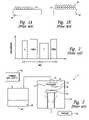
- FIGS. 1A and 1Bare schematic cross-sectional views of stages in ALD processing in accordance with the prior art.
- FIG. 2is a graph illustrating a cycle for forming a layer using ALD techniques in accordance with the prior art.
- FIG. 3is a schematic representation of a system including a reaction chamber for depositing materials onto a microfeature workpiece in accordance with the prior art.
- FIG. 4is a schematic representation of a system for depositing materials onto a microfeature workpiece W in accordance with one embodiment of the invention.
- FIG. 5is a schematic representation of an ampoule for use in processing microfeature workpieces in accordance with another embodiment of the invention.
- FIG. 6is a schematic representation of an ampoule for use in processing microfeature workpieces in accordance with another embodiment of the invention.
- FIG. 7is a schematic representation of an ampoule for use in processing microfeature workpieces in accordance with another embodiment of the invention.
- FIG. 8Ais a schematic representation of an ampoule for use in processing microfeature workpieces in accordance with another embodiment of the invention.
- FIG. 8Bis a top plan view of one of the trays in the precursor exposure assembly of FIG. 8A .
- FIG. 9is a top plan view of a precursor exposure assembly for use in an ampoule in accordance with another embodiment of the invention.
- microfeature workpieceis used throughout to include substrates upon which and/or in which microelectronic devices, micromechanical devices, data storage elements, read/write components, and other features are fabricated.
- microfeature workpiecescan be semiconductor wafers such as silicon or gallium arsenide wafers, glass substrates, insulative substrates, and many other types of materials.
- gasis used throughout to include any form of matter that has no fixed shape and will conform in volume to the space available, which specifically includes vapors (i.e., a gas having a temperature less than the critical temperature so that it may be liquefied or solidified by compression at a constant temperature).
- vaporsi.e., a gas having a temperature less than the critical temperature so that it may be liquefied or solidified by compression at a constant temperature.
- an ampoulein one embodiment, includes a vessel having an interior volume configured to receive a precursor with a headspace above the precursor.
- the ampoulefurther includes a carrier gas inlet for flowing carrier gas into the vessel, a conduit having an opening in the precursor and an outlet in the headspace, and a flow driver for flowing the precursor through the conduit and into the headspace to increase the surface area of the precursor exposed to the carrier gas.
- the flow drivercan include a pump or a carrier gas line configured to flow carrier gas into the conduit. The carrier gas entrains molecules of the precursor as the carrier gas flows into and through the conduit.
- an ampoulein another embodiment, includes a vessel having an interior volume configured to receive a precursor with a headspace above the precursor.
- the ampoulefurther includes a conduit for conveying a flow of the precursor to the headspace, a carrier gas inlet for flowing carrier gas into the vessel, and a precursor exposure assembly at least partially within the headspace.
- the precursor exposure assemblyis positioned so that at least some of the nonvaporized precursor flows from the conduit onto the assembly to increase the surface area of the precursor exposed to the carrier gas.
- the precursor exposure assemblycan include a plurality of channels, a conical surface, and/or a plurality of trays arranged in a stack to hold discrete volumes of precursor.
- a methodincludes delivering carrier gas to a vessel having a precursor and a headspace above the precursor, flowing the precursor through a conduit into the headspace to increase the surface area of the precursor exposed to the carrier gas, and removing from the headspace a reaction gas comprised of vaporized precursor.
- Flowing the precursor through the conduitcan include entraining molecules of the precursor in a carrier gas that passes through the conduit.
- flowing the precursor through the conduitcan include pumping the precursor through the conduit with a pump.
- the methodcan further include passing the reaction gas from the headspace to the reaction chamber and depositing a reaction product on a surface of the microfeature workpiece.
- the reaction productcan be derived, at least in part, from the vaporized precursor.
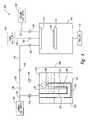
- FIG. 4is a schematic representation of a system 100 for depositing materials onto a microfeature workpiece W in accordance with one embodiment of the invention.
- the illustrated system 100includes a gas phase reaction chamber 110 for receiving the workpiece W, an ampoule 160 for carrying a precursor 170 , and a carrier gas supply 130 for providing carrier gas to the ampoule 160 to facilitate transport of the precursor 170 to the reaction chamber 110 .
- the carrier gasmixes with precursor 170 in the ampoule 160 to form a reaction gas.
- the reaction gasis delivered to the reaction chamber 110 and deposits a layer of material onto the surface of the workpiece W.
- the illustrated system 100further includes a carrier gas supply line 132 to convey the flow of carrier gas to the ampoule 160 , and a reaction gas delivery line 140 to convey the flow of reaction gas from the ampoule 160 to the reaction chamber 110 .
- Gas flow through the supply line 132 and the delivery line 140can be regulated by one or more valves.
- the gas flowcan be regulated by an ampoule inlet valve 134 , an ampoule outlet valve 142 , a delivery line valve 144 (shown in hidden lines), and a chamber inlet valve 146 (shown in hidden lines).
- a bypass line 136(shown in hidden lines) with a valve 138 (shown in hidden lines) may deliver carrier gas directly from the supply line 132 to the delivery line 140 to control the concentration of the vaporized precursor in the reaction gas.
- a second precursor and a purge gasmay be delivered from a second gas supply 150 (shown schematically and in hidden lines) and a third gas supply 155 (shown schematically and in hidden lines), respectively.
- the second gas supply 150can be coupled to the reaction chamber 110 via a delivery line 152 (shown in hidden lines) having a valve 154 (shown in hidden lines) to control the flow of the second precursor
- the third gas supply 155can be coupled to the reaction chamber 110 via a delivery line 156 (shown in hidden lines) having a valve 158 (shown in hidden lines) to control the flow of the purge gas.
- the first and second precursorscan be the gas and/or vapor phase constituents that react to form the thin, solid layer on the workpiece W.
- the purge gascan be a suitable type of gas that is compatible with the reaction chamber 110 and the workpiece W.
- the system 100can include a different number of gas sources for applications that require additional precursors or purge gases.
- the illustrated reaction chamber 110includes a gas dispenser 112 to flow the gas(es) onto the workpiece W and a workpiece support 114 to hold the workpiece W.
- the workpiece support 114can be heated to bring the workpiece W to a desired temperature for catalyzing the reaction between the first and second precursors at the surface of the workpiece W.
- the workpiece support 114can be a plate with a heating element.
- the workpiece support 114may not be heated in other applications.
- a vacuum 116(shown schematically) maintains negative pressure in the reaction chamber 110 to draw the gas(es) from the gas dispenser 112 across the workpiece W and then through an outlet of the reaction chamber 110 .
- the illustrated ampoule 160includes a vessel 162 having an interior volume configured to receive the precursor 170 with a headspace 178 above the precursor 170 .
- the vessel 162should be made of a material that is relatively inert with respect to the precursor 170 such that contact between the precursor 170 and the interior surface of the vessel 162 does not unduly degrade the vessel 162 or contaminate the precursor 170 .
- the material of the vessel 162should also be selected to withstand the rigors of use, which may include elevated processing temperatures, corrosive fluids, and/or friction with an abrasive particulate precursor. Suitable materials for forming the vessel 162 can include ceramics, glass, and metals such as stainless steel.
- the illustrated ampoule 160further includes a gas conduit 164 in fluid communication with the supply line 132 to convey a flow of carrier gas within the vessel 162 .
- the gas conduit 164has an opening 166 in the precursor 170 and an outlet 168 in the headspace 178 .
- the opening 166is sized and positioned so that precursor 170 flows into the gas conduit 164 and becomes entrained in the carrier gas as the carrier gas flows through the conduit 164 . Because the mixture of carrier gas and entrained precursor 172 is less dense than the liquid precursor 170 , the entrained precursor 172 flows up the gas conduit 164 and through the outlet 168 .
- the portion of the gas conduit 164 between the opening 166 and the outlet 168defines a lift tube 167 to convey a flow of entrained precursor 172 to the headspace 178 .
- the lift tube 167can have a hollow circular, rectangular, triangular, or other suitable cross-sectional configuration to convey the flow of entrained precursor 172 .
- the entrained precursor 172vaporizes as the precursor 172 is exposed to the carrier gas.
- the vaporized precursoris subsequently removed from the headspace 178 via the gas delivery line 140 .
- the nonvaporized precursor 170flows from the outlet 168 and back toward the precursor 170 at the base of the vessel 162 . Additional amounts of the precursor 170 vaporize in the headspace 178 because the nonvaporized precursor 170 flowing between the outlet 168 and the liquid precursor 170 at the base of the vessel 162 is exposed to the carrier gas.
- the precursor 170is exposed to the carrier gas in the lift tube 167 , at the surface of the liquid precursor 170 , and in the external flow from the outlet 168 of the lift tube 167 .
- One feature of the ampoule 160 illustrated in FIG. 4is that the lift tube 167 increases the surface area of the precursor exposed to the carrier gas. Because the precursor is exposed to the carrier gas as the precursor flows through the lift tube 167 and from the outlet 168 toward the base of the vessel 162 , the surface area of the precursor exposed to the carrier gas is greater than the transverse cross-sectional area of the vessel 162 .
- An advantage of this featureis that the vaporization rate of the precursor in the vessel 162 is increased because the vaporization rate is generally proportional to the exposed surface area of the precursor. As such, certain low volatility precursors that do not vaporize in prior art ampoules at a sufficient rate for a commercially acceptable production throughput may vaporize at commercially acceptable rates in the ampoule 160 illustrated in FIG. 4 .
- Another feature of the ampoule 160 illustrated in FIG. 4is that the vaporization rate of the precursor is increased without increasing the flow rate of the carrier gas.
- An advantage of this featureis that the vaporization rate of the precursor is increased without reducing the concentration of precursor in the carrier gas.
- FIG. 5is a schematic representation of an ampoule 260 for use in processing microfeature workpieces in accordance with another embodiment of the invention.
- the illustrated ampoule 260is generally similar to the ampoule 160 described above with reference to FIG. 4 .
- the illustrated ampoule 260includes a gas conduit 264 and a discrete lift tube 267 spaced apart from the gas conduit 264 .
- the gas conduit 264includes an outlet 265
- the lift tube 267includes an opening 266 in the precursor 170 and an outlet 268 in the headspace 178 .
- the lift tube 267may also include a tapered portion 269 at the opening 266 so that the cross-sectional area of the opening 266 is greater than the cross-sectional area of the outlet 268 .
- the opening 266 of the lift tube 267 and the outlet 265 of the gas conduit 264are positioned relative to each other so that carrier gas 263 flows from the outlet 265 into the lift tube 267 .
- the carrier gas 263entrains precursor 172 as the gas 263 flows through the lift tube 267 , and some of the entrained precursor 172 vaporizes in the lift tube 267 .
- Some of the nonvaporized precursor 170may also vaporize as the precursor 170 flows from the outlet 268 of the lift tube 267 toward the liquid precursor 170 at the base of the vessel 162 .
- the illustrated lift tube 267increases the surface area of the precursor exposed to carrier gas so that the ampoule 260 advantageously increases the vaporization rate of the precursor.
- FIG. 6is a schematic representation of an ampoule 360 for use in processing microfeature workpieces in accordance with another embodiment of the invention.
- the illustrated ampoule 360is generally similar to the ampoule 260 described above with reference to FIG. 5 .
- the ampoule 360includes a lift tube 367 with an opening 366 in the precursor 170 and an outlet 368 in the headspace 178 .
- the illustrated ampoule 360does not entrain precursor in a flow of carrier gas passing through the lift tube. Rather, the ampoule 360 includes a pump 369 (shown schematically) to flow the precursor 170 through the lift tube 367 and into the headspace 178 .
- the pump 369can be submerged in the precursor 170 , positioned in the headspace 178 , or located at another suitable position to flow precursor 170 through the lift tube 367 .
- the precursor 170is exposed to carrier gas, which is delivered to the vessel 162 via a carrier gas inlet 361 . Exposure to the carrier gas causes some of the precursor 170 to vaporize. The nonvaporized precursor 170 flows back toward the liquid precursor 170 at the base of the vessel 162 for recirculation through the lift tube 367 .
- the illustrated ampoule 360increases the surface area of the precursor 170 exposed to the carrier gas and, consequently, the vaporization rate of the precursor 170 .
- FIG. 7is a schematic representation of an ampoule 460 for use in processing microfeature workpieces in accordance with another embodiment of the invention.
- the illustrated ampoule 460is generally similar to the ampoule 160 described above with reference to FIG. 4 .
- the illustrated ampoule 460further includes a precursor exposure assembly 480 for increasing the surface area of the precursor 170 exposed to the carrier gas.
- the illustrated precursor exposure assembly 480includes a conical member 482 having a surface 484 positioned proximate to the outlet 168 of the gas conduit 164 so that the nonvaporized precursor 170 falls onto the surface 484 after exiting the outlet 168 .
- the slope of the conical member 482conveys the flow of nonvaporized precursor 170 across the surface 484 in a direction S 1 .
- the precursor exposure assembly 480increases the vaporization rate of the precursor 170 by increasing the exposure of the precursor 170 to the carrier gas.
- FIG. 8Ais a schematic representation of an ampoule 560 for use in processing microfeature workpieces in accordance with another embodiment of the invention.
- the illustrated ampoule 560is generally similar to the ampoule 160 described above with reference to FIG. 4 .
- the illustrated ampoule 560includes a precursor exposure assembly 580 for increasing the surface area of the precursor 170 exposed to the carrier gas.
- the illustrated precursor exposure assembly 580includes a plurality of trays 582 arranged in a stack and positioned proximate to the outlet 168 of the gas conduit 164 .
- the trays 582hold discrete volumes of precursor 170 to increase the surface area of the precursor 170 exposed to the carrier gas.
- the nonvaporized precursor 170flows from the outlet 168 of the gas conduit 164 and into a top tray 582 a .
- the individual trays 582are configured so that cascading flows 176 of precursor 170 pass downward from one tray 582 to an adjacent tray 582 .
- the gas conduit 164can include a plurality of holes to flow nonvaporized precursor 170 directly into the individual trays 582 in lieu of or in addition to the flow from the outlet 168 to the top tray 582 a.
- FIG. 8Bis a top plan view of one of the trays 582 of the precursor exposure assembly 580 of FIG. 8A without the precursor 170 .
- the illustrated trays 582include a support surface 583 , a hole 584 in the support surface 583 , and an outer wall 586 projecting from the support surface 583 .
- the hole 584is sized to receive the gas conduit 164 ( FIG. 8A ) so that the trays 582 can be arranged around the conduit 164 .
- the outer wall 586 and the support surface 583define an interior region configured to carry the nonvaporized precursor 170 .
- the trays 582can also include a plurality of notches 588 in the outer wall 586 through which the nonvaporized precursor 170 flows to an adjacent tray 582 . More specifically, the outer wall 586 has a height H 1 ( FIG. 8A ) and is positioned at a radius R 1 ( FIG. 8B ) on the trays 582 . The notches 588 have a height H 2 ( FIG. 8A ) and are positioned at a radius R 2 ( FIG. 8B ) less than the radius R 1 .
- the trays 582can be arranged with the notches 588 on adjacent trays 582 offset from each other so that the nonvaporized precursor 170 can flow downwardly into the adjacent tray 582 .
- the precursor exposure assembly 580can have other configurations.
- the trays 582may not include notches 588 , and/or the individual trays may have different diameters.
- the gas conduit 164can be positioned to flow nonvaporized precursor 170 into the trays 582 without extending through the center of the tray stack.
- One feature of the ampoule 560 illustrated in FIGS. 8A and 8Bis that the trays 582 of the precursor exposure assembly 580 carry discrete volumes of precursor 170 .
- An advantage of this featureis that the vaporization rate of the precursor 170 is increased due to the large surface area of the precursor 170 exposed to the carrier gas.
- the trays 582provide a relatively constant surface area that helps stabilize the vaporization rate of the precursor 170 and lends greater control to the concentration of the vaporized precursor 170 in the reaction gas extracted from the vessel 162 .
- FIG. 9is a top plan view of a precursor exposure assembly 680 for use in an ampoule in accordance with another embodiment of the invention.
- the illustrated precursor exposure assembly 680includes a central member 681 and a plurality of channels 682 projecting radially outward from the central member 681 .
- the central member 681includes a hole 684 sized to receive a gas conduit so that the channels 682 can be positioned around the outlet of the gas conduit.
- the channels 682can project radially outward and generally normal to the gas conduit, or alternatively, the channels 682 can project radially outward and downward toward the precursor at the base of the vessel.
- the channels 682are configured to receive some of the nonvaporized precursor as it flows from the gas conduit to increase the surface area of the nonvaporized precursor exposed to the carrier gas.
- the channels 682can include a support surface 683 and sidewalls 686 projecting from the support surface 683 .
- the sidewalls 686ensure that the nonvaporized precursor flows across the support surface 683 in a direction S 2 so that the surface area of the precursor exposed to the carrier gas is predictable and consistent over time.
- the channels 682may not have sidewalls 686 or may have other configurations.
Landscapes
- Chemical & Material Sciences (AREA)
- General Chemical & Material Sciences (AREA)
- Chemical Kinetics & Catalysis (AREA)
- Engineering & Computer Science (AREA)
- Materials Engineering (AREA)
- Mechanical Engineering (AREA)
- Metallurgy (AREA)
- Organic Chemistry (AREA)
- Chemical Vapour Deposition (AREA)
Abstract
Description
Claims (17)
Priority Applications (1)
| Application Number | Priority Date | Filing Date | Title |
|---|---|---|---|
| US10/814,573US7584942B2 (en) | 2004-03-31 | 2004-03-31 | Ampoules for producing a reaction gas and systems for depositing materials onto microfeature workpieces in reaction chambers |
Applications Claiming Priority (1)
| Application Number | Priority Date | Filing Date | Title |
|---|---|---|---|
| US10/814,573US7584942B2 (en) | 2004-03-31 | 2004-03-31 | Ampoules for producing a reaction gas and systems for depositing materials onto microfeature workpieces in reaction chambers |
Publications (2)
| Publication Number | Publication Date |
|---|---|
| US20050217575A1 US20050217575A1 (en) | 2005-10-06 |
| US7584942B2true US7584942B2 (en) | 2009-09-08 |
Family
ID=35052870
Family Applications (1)
| Application Number | Title | Priority Date | Filing Date |
|---|---|---|---|
| US10/814,573Expired - Fee RelatedUS7584942B2 (en) | 2004-03-31 | 2004-03-31 | Ampoules for producing a reaction gas and systems for depositing materials onto microfeature workpieces in reaction chambers |
Country Status (1)
| Country | Link |
|---|---|
| US (1) | US7584942B2 (en) |
Cited By (1)
| Publication number | Priority date | Publication date | Assignee | Title |
|---|---|---|---|---|
| US20130175362A1 (en)* | 2012-01-06 | 2013-07-11 | Chung-Ming Lee | Droplets straining device and atomizer comprising the same |
Families Citing this family (21)
| Publication number | Priority date | Publication date | Assignee | Title |
|---|---|---|---|---|
| US6838114B2 (en) | 2002-05-24 | 2005-01-04 | Micron Technology, Inc. | Methods for controlling gas pulsing in processes for depositing materials onto micro-device workpieces |
| US6821347B2 (en) | 2002-07-08 | 2004-11-23 | Micron Technology, Inc. | Apparatus and method for depositing materials onto microelectronic workpieces |
| US6955725B2 (en) | 2002-08-15 | 2005-10-18 | Micron Technology, Inc. | Reactors with isolated gas connectors and methods for depositing materials onto micro-device workpieces |
| US6926775B2 (en) | 2003-02-11 | 2005-08-09 | Micron Technology, Inc. | Reactors with isolated gas connectors and methods for depositing materials onto micro-device workpieces |
| US7335396B2 (en) | 2003-04-24 | 2008-02-26 | Micron Technology, Inc. | Methods for controlling mass flow rates and pressures in passageways coupled to reaction chambers and systems for depositing material onto microfeature workpieces in reaction chambers |
| US7422635B2 (en) | 2003-08-28 | 2008-09-09 | Micron Technology, Inc. | Methods and apparatus for processing microfeature workpieces, e.g., for depositing materials on microfeature workpieces |
| US7056806B2 (en) | 2003-09-17 | 2006-06-06 | Micron Technology, Inc. | Microfeature workpiece processing apparatus and methods for controlling deposition of materials on microfeature workpieces |
| US7258892B2 (en) | 2003-12-10 | 2007-08-21 | Micron Technology, Inc. | Methods and systems for controlling temperature during microfeature workpiece processing, e.g., CVD deposition |
| US7906393B2 (en) | 2004-01-28 | 2011-03-15 | Micron Technology, Inc. | Methods for forming small-scale capacitor structures |
| US8133554B2 (en) | 2004-05-06 | 2012-03-13 | Micron Technology, Inc. | Methods for depositing material onto microfeature workpieces in reaction chambers and systems for depositing materials onto microfeature workpieces |
| US7699932B2 (en) | 2004-06-02 | 2010-04-20 | Micron Technology, Inc. | Reactors, systems and methods for depositing thin films onto microfeature workpieces |
| US7422983B2 (en)* | 2005-02-24 | 2008-09-09 | International Business Machines Corporation | Ta-TaN selective removal process for integrated device fabrication |
| US7638074B2 (en) | 2006-03-10 | 2009-12-29 | Advanced Technology Materials, Inc. | Precursor compositions for atomic layer deposition and chemical vapor deposition of titanate, lanthanate, and tantalate dielectric films |
| US8455049B2 (en)* | 2007-08-08 | 2013-06-04 | Advanced Technology Materials, Inc. | Strontium precursor for use in chemical vapor deposition, atomic layer deposition and rapid vapor deposition |
| US8459293B2 (en)* | 2009-04-24 | 2013-06-11 | Applied Materials, Inc. | Ampoule with integrated hybrid valve |
| US9373677B2 (en) | 2010-07-07 | 2016-06-21 | Entegris, Inc. | Doping of ZrO2 for DRAM applications |
| KR101389011B1 (en)* | 2012-03-28 | 2014-04-24 | 주식회사 유니텍스 | Source container and reactor for vapor phase deposition |
| WO2013177326A1 (en) | 2012-05-25 | 2013-11-28 | Advanced Technology Materials, Inc. | Silicon precursors for low temperature ald of silicon-based thin-films |
| WO2014124056A1 (en) | 2013-02-08 | 2014-08-14 | Advanced Technology Materials, Inc. | Ald processes for low leakage current and low equivalent oxide thickness bitao films |
| US10619243B2 (en) | 2016-07-22 | 2020-04-14 | Triratna P. Muneshwar | Method to improve precursor utilization in pulsed atomic layer processes |
| US20230124304A1 (en)* | 2021-10-14 | 2023-04-20 | Applied Materials, Inc. | Controlled delivery of low-vapor-pressure precursor into a chamber |
Citations (412)
| Publication number | Priority date | Publication date | Assignee | Title |
|---|---|---|---|---|
| US579269A (en) | 1897-03-23 | Roller-bearing | ||
| US1741519A (en)* | 1926-12-10 | 1929-12-31 | Universal Oil Prod Co | Dephlegmator or fractionating column |
| US2508500A (en) | 1942-05-23 | 1950-05-23 | Hartford Nat Bank & Trust Co | Apparatus for applying metal coatings on insulators |
| USRE24291E (en)* | 1957-03-19 | Device for introducing atomized liquid into gas under pressure | ||
| US3522836A (en) | 1966-07-06 | 1970-08-04 | Battelle Development Corp | Method of manufacturing wire and the like |
| US3618919A (en) | 1969-11-03 | 1971-11-09 | Btu Eng Corp | Adjustable heat and gas barrier |
| US3620934A (en) | 1966-08-08 | 1971-11-16 | Fer Blanc Sarl Centre Rech Du | Method of electrolytic tinning sheet steel |
| US3630769A (en) | 1968-04-24 | 1971-12-28 | Plessey Co Ltd | PRODUCTION OF VAPOR-DEPOSITED Nb{11 B{11 Sn CONDUCTOR MATERIAL |
| US3630881A (en) | 1970-01-22 | 1971-12-28 | Ibm | Cathode-target assembly for rf sputtering apparatus |
| US3634212A (en) | 1970-05-06 | 1972-01-11 | M & T Chemicals Inc | Electrodeposition of bright acid tin and electrolytes therefor |
| US3744771A (en)* | 1970-07-20 | 1973-07-10 | Ahldea Corp | Disposable liquid entraining system |
| US3945804A (en)* | 1972-09-06 | 1976-03-23 | Sun Ventures, Inc. | Ammoxidation apparatus |
| US4018949A (en) | 1976-01-12 | 1977-04-19 | Ford Motor Company | Selective tin deposition onto aluminum piston skirt areas |
| SU598630A1 (en) | 1974-08-15 | 1978-02-21 | Предприятие П/Я Р-6707 | Device for introducing into reaction chamber |
| US4242182A (en) | 1978-07-21 | 1980-12-30 | Francine Popescu | Bright tin electroplating bath |
| US4269625A (en) | 1978-12-04 | 1981-05-26 | U.S. Philips Corporation | Bath for electroless depositing tin on substrates |
| US4289061A (en) | 1977-10-03 | 1981-09-15 | Hooker Chemicals & Plastics Corp. | Device and assembly for mounting parts |
| US4313783A (en) | 1980-05-19 | 1982-02-02 | Branson International Plasma Corporation | Computer controlled system for processing semiconductor wafers |
| US4388342A (en) | 1979-05-29 | 1983-06-14 | Hitachi, Ltd. | Method for chemical vapor deposition |
| US4397753A (en) | 1982-09-20 | 1983-08-09 | Circuit Chemistry Corporation | Solder stripping solution |
| US4436674A (en) | 1981-07-30 | 1984-03-13 | J.C. Schumacher Co. | Vapor mass flow control system |
| US4438724A (en) | 1982-08-13 | 1984-03-27 | Energy Conversion Devices, Inc. | Grooved gas gate |
| US4469801A (en) | 1980-09-04 | 1984-09-04 | Toshio Hirai | Titanium-containing silicon nitride film bodies and a method of producing the same |
| US4509456A (en) | 1981-07-28 | 1985-04-09 | Veb Zentrum Fur Forschung Und Technologie Mikroelektronik | Apparatus for guiding gas for LP CVD processes in a tube reactor |
| US4545136A (en) | 1981-03-16 | 1985-10-08 | Sovonics Solar Systems | Isolation valve |
| US4590042A (en) | 1984-12-24 | 1986-05-20 | Tegal Corporation | Plasma reactor having slotted manifold |
| US4593644A (en) | 1983-10-26 | 1986-06-10 | Rca Corporation | Continuous in-line deposition system |
| US4595399A (en)* | 1984-11-05 | 1986-06-17 | The United States Of America As Represented By The Administrator Of The National Aeronautics And Space Administration | Nebulization reflux concentrator |
| US4681777A (en) | 1986-05-05 | 1987-07-21 | Engelken Robert D | Method for electroless and vapor deposition of thin films of three tin sulfide phases on conductive and nonconductive substrates |
| JPS62235728A (en) | 1986-04-07 | 1987-10-15 | Nec Corp | Vapor phase epitaxial growth device |
| JPS62263629A (en) | 1986-05-12 | 1987-11-16 | Hitachi Ltd | Vapor phase growth equipment |
| US4738295A (en) | 1985-04-02 | 1988-04-19 | Genser Hans G | Method and apparatus for evaporating a fluid in a rotating vacuum evaporation system |
| JPS6320490Y2 (en) | 1979-09-08 | 1988-06-07 | ||
| JPS63111177U (en) | 1987-01-12 | 1988-07-16 | ||
| JPS63234198A (en) | 1987-03-24 | 1988-09-29 | 株式会社東芝 | Flange image leakage detection device |
| JPS63256460A (en) | 1987-04-14 | 1988-10-24 | Oki Electric Ind Co Ltd | Substrate for thermal head and production thereof |
| US4780178A (en) | 1982-10-15 | 1988-10-25 | Yamoto Scientific Co. Ltd. | Rotary evaporator with control system |
| US4826579A (en) | 1982-06-25 | 1989-05-02 | Cel Systems Corporation | Electrolytic preparation of tin and other metals |
| US4832115A (en) | 1986-07-09 | 1989-05-23 | Albers Technologies Corporation | Method and apparatus for simultaneous heat and mass transfer |
| US4871417A (en) | 1986-07-04 | 1989-10-03 | Dainippon Screen Mfg. Co., Ltd. | Method and apparatus for surface treating of substrates |
| JPH01273991A (en) | 1988-04-26 | 1989-11-01 | Ishikawajima Harima Heavy Ind Co Ltd | Furnace sealing device |
| US4894132A (en) | 1987-10-21 | 1990-01-16 | Mitsubishi Denki Kabushiki Kaisha | Sputtering method and apparatus |
| US4911638A (en) | 1989-05-18 | 1990-03-27 | Direction Incorporated | Controlled diffusion environment capsule and system |
| US4923715A (en) | 1986-03-31 | 1990-05-08 | Kabushiki Kaisha Toshiba | Method of forming thin film by chemical vapor deposition |
| US4948979A (en) | 1987-12-21 | 1990-08-14 | Kabushiki Kaisha Toshiba | Vacuum device for handling workpieces |
| US4949669A (en) | 1988-12-20 | 1990-08-21 | Texas Instruments Incorporated | Gas flow systems in CCVD reactors |
| US4966646A (en) | 1986-09-24 | 1990-10-30 | Board Of Trustees Of Leland Stanford University | Method of making an integrated, microminiature electric-to-fluidic valve |
| US4977106A (en) | 1990-05-01 | 1990-12-11 | Texas Instruments Incorporated | Tin chemical vapor deposition using TiCl4 and SiH4 |
| US5015330A (en) | 1989-02-28 | 1991-05-14 | Kabushiki Kaisha Toshiba | Film forming method and film forming device |
| US5017404A (en) | 1988-09-06 | 1991-05-21 | Schott Glaswerke | Plasma CVD process using a plurality of overlapping plasma columns |
| US5020476A (en) | 1990-04-17 | 1991-06-04 | Ds Research, Inc. | Distributed source assembly |
| JPH03174717A (en) | 1989-10-06 | 1991-07-29 | Nippon Kentetsu Co Ltd | Method of supplying water of plasma ashing |
| US5062446A (en) | 1991-01-07 | 1991-11-05 | Sematech, Inc. | Intelligent mass flow controller |
| US5076205A (en) | 1989-01-06 | 1991-12-31 | General Signal Corporation | Modular vapor processor system |
| US5091207A (en) | 1989-07-20 | 1992-02-25 | Fujitsu Limited | Process and apparatus for chemical vapor deposition |
| US5090985A (en) | 1989-10-17 | 1992-02-25 | Libbey-Owens-Ford Co. | Method for preparing vaporized reactants for chemical vapor deposition |
| JPH04100533A (en) | 1990-08-18 | 1992-04-02 | Mitsubishi Electric Corp | vacuum container |
| US5131752A (en) | 1990-06-28 | 1992-07-21 | Tamarack Scientific Co., Inc. | Method for film thickness endpoint control |
| JPH04213818A (en) | 1990-12-07 | 1992-08-04 | Sony Corp | Cvd device |
| US5136975A (en) | 1990-06-21 | 1992-08-11 | Watkins-Johnson Company | Injector and method for delivering gaseous chemicals to a surface |
| US5172849A (en) | 1991-09-25 | 1992-12-22 | General Motors Corporation | Method and apparatus for convection brazing of aluminum heat exchangers |
| US5200023A (en) | 1991-08-30 | 1993-04-06 | International Business Machines Corp. | Infrared thermographic method and apparatus for etch process monitoring and control |
| US5223113A (en) | 1990-07-20 | 1993-06-29 | Tokyo Electron Limited | Apparatus for forming reduced pressure and for processing object |
| US5232749A (en) | 1991-04-30 | 1993-08-03 | Micron Technology, Inc. | Formation of self-limiting films by photoemission induced vapor deposition |
| US5248527A (en) | 1991-03-01 | 1993-09-28 | C. Uyemura And Company, Limited | Process for electroless plating tin, lead or tin-lead alloy |
| US5286296A (en) | 1991-01-10 | 1994-02-15 | Sony Corporation | Multi-chamber wafer process equipment having plural, physically communicating transfer means |
| JPH06151558A (en) | 1992-11-09 | 1994-05-31 | Tokyo Electron Ltd | Transfer processing device |
| US5325020A (en) | 1990-09-28 | 1994-06-28 | Abtox, Inc. | Circular waveguide plasma microwave sterilizer apparatus |
| JPH06201539A (en) | 1993-01-04 | 1994-07-19 | Yasuo Kitsuta | Centrifugal evaporator |
| JPH06202372A (en) | 1992-10-21 | 1994-07-22 | Hewlett Packard Co <Hp> | Toner composition and its adjusting method |
| US5364219A (en) | 1991-06-24 | 1994-11-15 | Tdk Corporation | Apparatus for clean transfer of objects |
| US5366557A (en) | 1990-06-18 | 1994-11-22 | At&T Bell Laboratories | Method and apparatus for forming integrated circuit layers |
| JPH06342785A (en) | 1993-06-01 | 1994-12-13 | Fujitsu Ltd | Exhauster of vapor growth device and cleaning method thereof |
| US5377429A (en) | 1993-04-19 | 1995-01-03 | Micron Semiconductor, Inc. | Method and appartus for subliming precursors |
| US5380396A (en) | 1991-05-30 | 1995-01-10 | Hitachi, Ltd. | Valve and semiconductor fabricating equipment using the same |
| US5409129A (en) | 1990-12-28 | 1995-04-25 | Hokkai Can Co., Ltd. | Welded cans |
| US5418180A (en) | 1994-06-14 | 1995-05-23 | Micron Semiconductor, Inc. | Process for fabricating storage capacitor structures using CVD tin on hemispherical grain silicon |
| US5427666A (en) | 1993-09-09 | 1995-06-27 | Applied Materials, Inc. | Method for in-situ cleaning a Ti target in a Ti + TiN coating process |
| US5433835A (en) | 1993-11-24 | 1995-07-18 | Applied Materials, Inc. | Sputtering device and target with cover to hold cooling fluid |
| US5433787A (en) | 1991-12-12 | 1995-07-18 | Canon Kabushiki Kaisha | Apparatus for forming deposited film including light transmissive diffusion plate |
| US5445491A (en) | 1991-08-27 | 1995-08-29 | Toshiba Kikai Kabushiki Kaisha | Method for multichamber sheet-after-sheet type treatment |
| US5453124A (en) | 1992-12-30 | 1995-09-26 | Texas Instruments Incorporated | Programmable multizone gas injector for single-wafer semiconductor processing equipment |
| US5474612A (en) | 1990-03-19 | 1995-12-12 | Kabushiki Kaisha Toshiba | Vapor-phase deposition apparatus and vapor-phase deposition method |
| US5477623A (en) | 1992-11-25 | 1995-12-26 | Matsushita Electric Industrial Co., Ltd. | Drying apparatus |
| US5480818A (en) | 1992-02-10 | 1996-01-02 | Fujitsu Limited | Method for forming a film and method for manufacturing a thin film transistor |
| JPH0834678A (en) | 1994-07-27 | 1996-02-06 | Matsushita Electric Works Ltd | Aerogel panel |
| US5496410A (en) | 1992-03-10 | 1996-03-05 | Hitachi, Ltd. | Plasma processing apparatus and method of processing substrates by using same apparatus |
| US5498292A (en) | 1994-06-16 | 1996-03-12 | Kishimoto Sangyo Co., Ltd. | Heating device used for a gas phase growing mechanism or heat treatment mechanism |
| US5500256A (en) | 1994-08-16 | 1996-03-19 | Fujitsu Limited | Dry process apparatus using plural kinds of gas |
| US5522934A (en) | 1994-04-26 | 1996-06-04 | Tokyo Electron Limited | Plasma processing apparatus using vertical gas inlets one on top of another |
| US5536317A (en) | 1995-10-27 | 1996-07-16 | Specialty Coating Systems, Inc. | Parylene deposition apparatus including a quartz crystal thickness/rate controller |
| US5562800A (en) | 1993-09-20 | 1996-10-08 | Hitachi, Ltd. | Wafer transport method |
| US5575883A (en) | 1993-07-09 | 1996-11-19 | Fujitsu Limited | Apparatus and process for fabricating semiconductor devices |
| US5589110A (en) | 1992-11-20 | 1996-12-31 | Mitsubishi Electric Corp | Container for liquid metal organic compound |
| US5589002A (en) | 1994-03-24 | 1996-12-31 | Applied Materials, Inc. | Gas distribution plate for semiconductor wafer processing apparatus with means for inhibiting arcing |
| US5592581A (en) | 1993-07-19 | 1997-01-07 | Tokyo Electron Kabushiki Kaisha | Heat treatment apparatus |
| US5595606A (en) | 1995-04-20 | 1997-01-21 | Tokyo Electron Limited | Shower head and film forming apparatus using the same |
| US5599513A (en) | 1989-11-13 | 1997-02-04 | Showa Denko K.K. | Gas distribution plate for use with fluidized-bed gas-phase polymerizer |
| US5609798A (en)* | 1995-06-07 | 1997-03-11 | Msp Corporation | High output PSL aerosol generator |
| JPH0982650A (en) | 1995-09-14 | 1997-03-28 | Kokusai Electric Co Ltd | Semiconductor manufacturing equipment |
| US5624498A (en) | 1993-12-22 | 1997-04-29 | Samsung Electronics Co., Ltd. | Showerhead for a gas supplying apparatus |
| US5626936A (en) | 1993-09-09 | 1997-05-06 | Energy Pillow, Inc. | Phase change insulation system |
| US5640751A (en) | 1995-07-17 | 1997-06-24 | Thermionics Laboratories, Inc. | Vacuum flange |
| US5643394A (en) | 1994-09-16 | 1997-07-01 | Applied Materials, Inc. | Gas injection slit nozzle for a plasma process reactor |
| US5654589A (en) | 1995-06-06 | 1997-08-05 | Advanced Micro Devices, Incorporated | Landing pad technology doubled up as local interconnect and borderless contact for deep sub-half micrometer IC application |
| US5658503A (en)* | 1996-02-01 | 1997-08-19 | Shell Oil Company | Dual phase distribution device |
| US5683538A (en) | 1994-12-23 | 1997-11-04 | International Business Machines Corporation | Control of etch selectivity |
| US5693288A (en) | 1994-06-24 | 1997-12-02 | Nisshin Steel Co., Ltd. | Seal assembly for thermal treatment furnaces using an atmospheric gas containing hydrogen gas |
| JPH108255A (en) | 1996-06-20 | 1998-01-13 | Ebara Corp | Liquid raw material vaporizing device |
| US5716796A (en) | 1990-01-23 | 1998-02-10 | Medical Devices Corporation | Optical blood hemostatic analysis apparatus and method |
| US5729896A (en) | 1996-10-31 | 1998-03-24 | International Business Machines Corporation | Method for attaching a flip chip on flexible circuit carrier using chip with metallic cap on solder |
| US5733375A (en) | 1995-01-06 | 1998-03-31 | Tokyo Electron Limited | Apparatus for supplying a treatment material |
| US5746434A (en) | 1996-07-09 | 1998-05-05 | Lam Research Corporation | Chamber interfacing O-rings and method for implementing same |
| US5754297A (en) | 1994-01-28 | 1998-05-19 | Applied Materials, Inc. | Method and apparatus for monitoring the deposition rate of films during physical vapor deposition |
| US5766364A (en) | 1996-07-17 | 1998-06-16 | Matsushita Electric Industrial Co., Ltd. | Plasma processing apparatus |
| US5769950A (en) | 1985-07-23 | 1998-06-23 | Canon Kabushiki Kaisha | Device for forming deposited film |
| US5769952A (en) | 1994-06-07 | 1998-06-23 | Tokyo Electron, Ltd. | Reduced pressure and normal pressure treatment apparatus |
| US5772771A (en) | 1995-12-13 | 1998-06-30 | Applied Materials, Inc. | Deposition chamber for improved deposition thickness uniformity |
| US5788778A (en) | 1996-09-16 | 1998-08-04 | Applied Komatsu Technology, Inc. | Deposition chamber cleaning technique using a high power remote excitation source |
| US5792269A (en) | 1995-10-31 | 1998-08-11 | Applied Materials, Inc. | Gas distribution for CVD systems |
| US5792700A (en) | 1996-05-31 | 1998-08-11 | Micron Technology, Inc. | Semiconductor processing method for providing large grain polysilicon films |
| JPH10223719A (en) | 1996-12-06 | 1998-08-21 | Dainippon Screen Mfg Co Ltd | Substrate carrier system, substrate processor and substrate carrier method |
| WO1998037258A1 (en) | 1997-02-25 | 1998-08-27 | Moore Epitaxial Inc. | A rapid thermal processing barrel reactor for processing substrates |
| US5803938A (en) | 1992-09-21 | 1998-09-08 | Mitsubishi Denki Kabushiki Kaisha | Liquid vaporizing apparatus |
| US5819683A (en) | 1995-05-02 | 1998-10-13 | Tokyo Electron Limited | Trap apparatus |
| US5820641A (en) | 1996-02-09 | 1998-10-13 | Mks Instruments, Inc. | Fluid cooled trap |
| US5820686A (en) | 1993-01-21 | 1998-10-13 | Moore Epitaxial, Inc. | Multi-layer susceptor for rapid thermal process reactors |
| US5827370A (en) | 1997-01-13 | 1998-10-27 | Mks Instruments, Inc. | Method and apparatus for reducing build-up of material on inner surface of tube downstream from a reaction furnace |
| US5833888A (en) | 1996-12-31 | 1998-11-10 | Atmi Ecosys Corporation | Weeping weir gas/liquid interface structure |
| US5846275A (en) | 1996-12-31 | 1998-12-08 | Atmi Ecosys Corporation | Clog-resistant entry structure for introducing a particulate solids-containing and/or solids-forming gas stream to a gas processing system |
| US5846330A (en) | 1997-06-26 | 1998-12-08 | Celestech, Inc. | Gas injection disc assembly for CVD applications |
| US5851849A (en) | 1997-05-22 | 1998-12-22 | Lucent Technologies Inc. | Process for passivating semiconductor laser structures with severe steps in surface topography |
| US5851294A (en) | 1995-10-23 | 1998-12-22 | Watkins-Johnson Company | Gas injection system for semiconductor processing |
| US5865417A (en) | 1996-09-27 | 1999-02-02 | Redwood Microsystems, Inc. | Integrated electrically operable normally closed valve |
| US5866986A (en) | 1996-08-05 | 1999-02-02 | Integrated Electronic Innovations, Inc. | Microwave gas phase plasma source |
| US5868159A (en) | 1996-07-12 | 1999-02-09 | Mks Instruments, Inc. | Pressure-based mass flow controller |
| WO1999006610A1 (en) | 1997-08-01 | 1999-02-11 | Applied Komatsu Technology, Inc. | Method and apparatus for detecting the endpoint of a chamber cleaning |
| US5879459A (en) | 1997-08-29 | 1999-03-09 | Genus, Inc. | Vertically-stacked process reactor and cluster tool system for atomic layer deposition |
| US5879516A (en) | 1996-02-29 | 1999-03-09 | Kasman; David H. | Kugelrohr or distillation apparatus |
| US5885425A (en) | 1995-06-06 | 1999-03-23 | International Business Machines Corporation | Method for selective material deposition on one side of raised or recessed features |
| US5895530A (en) | 1996-02-26 | 1999-04-20 | Applied Materials, Inc. | Method and apparatus for directing fluid through a semiconductor processing chamber |
| US5902403A (en) | 1995-11-28 | 1999-05-11 | Applied Materials, Inc. | Method and apparatus for cleaning a chamber |
| US5908947A (en) | 1996-02-09 | 1999-06-01 | Micron Technology, Inc. | Difunctional amino precursors for the deposition of films comprising metals |
| US5911238A (en) | 1996-10-04 | 1999-06-15 | Emerson Electric Co. | Thermal mass flowmeter and mass flow controller, flowmetering system and method |
| JPH11172438A (en) | 1997-09-29 | 1999-06-29 | Samsung Electron Co Ltd | Method for forming metal nitride film by chemical vapor deposition and method for forming metal contact of semiconductor device using the same |
| US5932286A (en) | 1993-03-16 | 1999-08-03 | Applied Materials, Inc. | Deposition of silicon nitride thin films |
| US5936829A (en) | 1997-01-02 | 1999-08-10 | Cvc Products, Inc. | Thermally conductive chuck for vacuum processor |
| US5940684A (en) | 1996-05-23 | 1999-08-17 | Rohm, Co., Ltd. | Method and equipment for manufacturing semiconductor device |
| US5953634A (en) | 1995-02-13 | 1999-09-14 | Kabushiki Kaisha Toshiba | Method of manufacturing semiconductor device |
| US5956613A (en) | 1995-12-27 | 1999-09-21 | Lsi Logic Corporation | Method for improvement of TiN CVD film quality |
| US5958140A (en) | 1995-07-27 | 1999-09-28 | Tokyo Electron Limited | One-by-one type heat-processing apparatus |
| US5963336A (en) | 1995-10-10 | 1999-10-05 | American Air Liquide Inc. | Chamber effluent monitoring system and semiconductor processing system comprising absorption spectroscopy measurement system, and methods of use |
| US5961775A (en) | 1987-08-19 | 1999-10-05 | Fujitsu Limited | Apparatus for removing organic resist from semiconductor |
| US5968587A (en) | 1996-11-13 | 1999-10-19 | Applied Materials, Inc. | Systems and methods for controlling the temperature of a vapor deposition apparatus |
| US5972430A (en) | 1997-11-26 | 1999-10-26 | Advanced Technology Materials, Inc. | Digital chemical vapor deposition (CVD) method for forming a multi-component oxide layer |
| US5994181A (en) | 1997-05-19 | 1999-11-30 | United Microelectronics Corp. | Method for forming a DRAM cell electrode |
| US5998932A (en) | 1998-06-26 | 1999-12-07 | Lam Research Corporation | Focus ring arrangement for substantially eliminating unconfined plasma in a plasma processing chamber |
| US5997588A (en) | 1995-10-13 | 1999-12-07 | Advanced Semiconductor Materials America, Inc. | Semiconductor processing system with gas curtain |
| US6006694A (en) | 1997-12-05 | 1999-12-28 | Tegal Corporation | Plasma reactor with a deposition shield |
| US6008086A (en) | 1995-10-24 | 1999-12-28 | Micron Technology, Inc. | Method of deposting uniform dielectric film deposition on textured surfaces |
| US6016611A (en) | 1998-07-13 | 2000-01-25 | Applied Komatsu Technology, Inc. | Gas flow control in a substrate processing system |
| US6022483A (en) | 1998-03-10 | 2000-02-08 | Intergrated Systems, Inc. | System and method for controlling pressure |
| US6032923A (en) | 1998-01-08 | 2000-03-07 | Xerox Corporation | Fluid valves having cantilevered blocking films |
| US6039557A (en) | 1989-12-22 | 2000-03-21 | Imarx Pharmaceutical Corp. | Apparatus for making gas-filled vesicles of optimal size |
| US6042652A (en) | 1999-05-01 | 2000-03-28 | P.K. Ltd | Atomic layer deposition apparatus for depositing atomic layer on multiple substrates |
| US6045620A (en) | 1997-07-11 | 2000-04-04 | Applied Materials, Inc. | Two-piece slit valve insert for vacuum processing system |
| US6059885A (en) | 1996-12-19 | 2000-05-09 | Toshiba Ceramics Co., Ltd. | Vapor deposition apparatus and method for forming thin film |
| DE19851824A1 (en) | 1998-11-10 | 2000-05-11 | Siemens Ag | Process for reducing deposits in a CVD reactor comprises rinsing the chamber walls with rinsing gas |
| US6062256A (en) | 1997-02-11 | 2000-05-16 | Engineering Measurements Company | Micro mass flow control apparatus and method |
| US6070551A (en) | 1996-05-13 | 2000-06-06 | Applied Materials, Inc. | Deposition chamber and method for depositing low dielectric constant films |
| US6079426A (en) | 1997-07-02 | 2000-06-27 | Applied Materials, Inc. | Method and apparatus for determining the endpoint in a plasma cleaning process |
| US6080446A (en) | 1997-08-21 | 2000-06-27 | Anelva Corporation | Method of depositing titanium nitride thin film and CVD deposition apparatus |
| US6086677A (en) | 1998-06-16 | 2000-07-11 | Applied Materials, Inc. | Dual gas faceplate for a showerhead in a semiconductor wafer processing system |
| WO2000040772A1 (en) | 1999-01-04 | 2000-07-13 | Genus, Inc. | Processing chamber for atomic layer deposition processes |
| US6089543A (en) | 1997-07-11 | 2000-07-18 | Applied Materials, Inc. | Two-piece slit valve door with molded-in-place seal for a vacuum processing system |
| US6090210A (en) | 1996-07-24 | 2000-07-18 | Applied Materials, Inc. | Multi-zone gas flow control in a process chamber |
| US6109206A (en) | 1997-05-29 | 2000-08-29 | Applied Materials, Inc. | Remote plasma source for chamber cleaning |
| US6113698A (en) | 1997-07-10 | 2000-09-05 | Applied Materials, Inc. | Degassing method and apparatus |
| US6123107A (en) | 1999-07-09 | 2000-09-26 | Redwood Microsystems, Inc. | Apparatus and method for mounting micromechanical fluid control components |
| US6129331A (en) | 1997-05-21 | 2000-10-10 | Redwood Microsystems | Low-power thermopneumatic microvalve |
| WO2000063952A1 (en) | 1999-04-15 | 2000-10-26 | Integrated Materials, Inc. | Silicon fixtures for wafer processing and method of fabrication |
| US6139700A (en) | 1997-10-01 | 2000-10-31 | Samsung Electronics Co., Ltd. | Method of and apparatus for forming a metal interconnection in the contact hole of a semiconductor device |
| WO2000065649A1 (en) | 1999-04-27 | 2000-11-02 | Tokyo Electron Limited | CVD TiN PLUG FORMATION FROM TITANIUM HALIDE PRECURSORS |
| US6143077A (en) | 1996-08-13 | 2000-11-07 | Anelva Corporation | Chemical vapor deposition apparatus |
| US6144060A (en) | 1997-07-31 | 2000-11-07 | Samsung Electronics Co., Ltd. | Integrated circuit devices having buffer layers therein which contain metal oxide stabilized by heat treatment under low temperature |
| US6143078A (en) | 1998-11-13 | 2000-11-07 | Applied Materials, Inc. | Gas distribution system for a CVD processing chamber |
| US6142163A (en) | 1996-03-29 | 2000-11-07 | Lam Research Corporation | Method and apparatus for pressure control in vacuum processors |
| US6143659A (en) | 1997-11-18 | 2000-11-07 | Samsung Electronics, Co., Ltd. | Method for manufacturing aluminum metal interconnection layer by atomic layer deposition method |
| US6159298A (en) | 1997-12-27 | 2000-12-12 | Tokyo Electron Limited | Thermal processing system |
| US6159297A (en) | 1996-04-25 | 2000-12-12 | Applied Materials, Inc. | Semiconductor process chamber and processing method |
| US6160243A (en) | 1998-09-25 | 2000-12-12 | Redwood Microsystems, Inc. | Apparatus and method for controlling fluid in a micromachined boiler |
| US6161500A (en) | 1997-09-30 | 2000-12-19 | Tokyo Electron Limited | Apparatus and method for preventing the premature mixture of reactant gases in CVD and PECVD reactions |
| US6173673B1 (en) | 1999-03-31 | 2001-01-16 | Tokyo Electron Limited | Method and apparatus for insulating a high power RF electrode through which plasma discharge gases are injected into a processing chamber |
| US6174366B1 (en) | 1993-12-23 | 2001-01-16 | Heikki Ihantola | Apparatus and method for processing of semiconductors, such as silicon chips |
| US6174809B1 (en) | 1997-12-31 | 2001-01-16 | Samsung Electronics, Co., Ltd. | Method for forming metal layer using atomic layer deposition |
| US6178660B1 (en) | 1999-08-03 | 2001-01-30 | International Business Machines Corporation | Pass-through semiconductor wafer processing tool and process for gas treating a moving semiconductor wafer |
| US6182603B1 (en) | 1998-07-13 | 2001-02-06 | Applied Komatsu Technology, Inc. | Surface-treated shower head for use in a substrate processing chamber |
| US6183563B1 (en) | 1998-05-18 | 2001-02-06 | Ips Ltd. | Apparatus for depositing thin films on semiconductor wafers |
| US6190459B1 (en) | 1998-01-07 | 2001-02-20 | Tokyo Electron Limited | Gas treatment apparatus |
| US6194628B1 (en) | 1995-09-25 | 2001-02-27 | Applied Materials, Inc. | Method and apparatus for cleaning a vacuum line in a CVD system |
| US6193802B1 (en) | 1995-09-25 | 2001-02-27 | Applied Materials, Inc. | Parallel plate apparatus for in-situ vacuum line cleaning for substrate processing equipment |
| US6192827B1 (en) | 1998-07-03 | 2001-02-27 | Applied Materials, Inc. | Double slit-valve doors for plasma processing |
| US6197119B1 (en) | 1999-02-18 | 2001-03-06 | Mks Instruments, Inc. | Method and apparatus for controlling polymerized teos build-up in vacuum pump lines |
| US6200415B1 (en) | 1999-06-30 | 2001-03-13 | Lam Research Corporation | Load controlled rapid assembly clamp ring |
| US6199465B1 (en)* | 1996-11-29 | 2001-03-13 | Fuji Koeki Co., Ltd. | Liquid coater |
| US6203613B1 (en) | 1999-10-19 | 2001-03-20 | International Business Machines Corporation | Atomic layer deposition with nitrate containing precursors |
| US6206972B1 (en) | 1999-07-08 | 2001-03-27 | Genus, Inc. | Method and apparatus for providing uniform gas delivery to substrates in CVD and PECVD processes |
| US6206967B1 (en) | 1997-12-02 | 2001-03-27 | Applied Materials, Inc. | Low resistivity W using B2H6 nucleation step |
| US6207937B1 (en) | 1998-05-11 | 2001-03-27 | Semitool, Inc. | Temperature control system for a thermal reactor |
| JP2001082682A (en) | 1999-09-10 | 2001-03-30 | Matsushita Refrig Co Ltd | Heat insulating material and heat insulating structure |
| US6211078B1 (en) | 1997-08-18 | 2001-04-03 | Micron Technology, Inc. | Method of improving resist adhesion for use in patterning conductive layers |
| US6210754B1 (en) | 1998-12-31 | 2001-04-03 | United Microelectronics Corp. | Method of adjusting for parallel alignment between a shower head and a heater platform in a chamber used in integrated circuit fabrication |
| US6211033B1 (en) | 1996-01-23 | 2001-04-03 | Micron Technology, Inc. | Integrated capacitor bottom electrode for use with conformal dielectric |
| US6214714B1 (en) | 1999-06-25 | 2001-04-10 | Applied Materials, Inc. | Method of titanium/titanium nitride integration |
| WO2001032966A1 (en) | 1999-11-02 | 2001-05-10 | Zakrytoe Aktsionernoe Obschestvo 'pandzhsher-Kholding' | Method for producing an initial polycrystalline silicon in the form of plates having a large surface and chamber for the precipitation of silicon |
| US6237394B1 (en) | 1999-02-25 | 2001-05-29 | Redwood Microsystems, Inc. | Apparatus and method for correcting drift in a sensor |
| US6237529B1 (en) | 2000-03-03 | 2001-05-29 | Eastman Kodak Company | Source for thermal physical vapor deposition of organic electroluminescent layers |
| US20010001952A1 (en) | 1984-07-26 | 2001-05-31 | Junichi Nishizawa | Semiconductor crystal growth apparatus |
| US6245192B1 (en) | 1999-06-30 | 2001-06-12 | Lam Research Corporation | Gas distribution apparatus for semiconductor processing |
| US6251190B1 (en) | 1997-06-30 | 2001-06-26 | Applied Materials, Inc. | Gate electrode connection structure by in situ chemical vapor deposition of tungsten and tungsten nitride |
| WO2001046490A1 (en) | 1999-12-22 | 2001-06-28 | Lam Research Corporation | Method of cleaning and conditioning plasma reaction chamber |
| US6255222B1 (en) | 1999-08-24 | 2001-07-03 | Applied Materials, Inc. | Method for removing residue from substrate processing chamber exhaust line for silicon-oxygen-carbon deposition process |
| US6264788B1 (en) | 1994-04-20 | 2001-07-24 | Tokyo Electron Limited | Plasma treatment method and apparatus |
| US6263829B1 (en) | 1999-01-22 | 2001-07-24 | Applied Materials, Inc. | Process chamber having improved gas distributor and method of manufacture |
| US20010010309A1 (en) | 2000-02-01 | 2001-08-02 | Van Bilsen Frank B. M. | System of controlling the temperature of a processing chamber |
| US6270572B1 (en) | 1998-08-07 | 2001-08-07 | Samsung Electronics Co., Ltd. | Method for manufacturing thin film using atomic layer deposition |
| US20010012697A1 (en) | 1996-04-03 | 2001-08-09 | Kabushiki Kaisha Toshiba | Apparatus for manufacturing a semiconductor device in a CVD reactive chamber |
| US6273954B2 (en) | 1998-09-03 | 2001-08-14 | Mitsubishi Denki Kabushiki Kaisha | System for manufacturing a semiconductor device |
| US6277763B1 (en) | 1999-12-16 | 2001-08-21 | Applied Materials, Inc. | Plasma processing of tungsten using a gas mixture comprising a fluorinated gas and oxygen |
| US6280584B1 (en) | 1998-07-29 | 2001-08-28 | Applied Materials, Inc. | Compliant bond structure for joining ceramic to metal |
| US6287965B1 (en) | 1997-07-28 | 2001-09-11 | Samsung Electronics Co, Ltd. | Method of forming metal layer using atomic layer deposition and semiconductor device having the metal layer as barrier metal layer or upper or lower electrode of capacitor |
| US6287980B1 (en) | 1999-04-22 | 2001-09-11 | Mitsubishi Denki Kabushiki Kaisha | Plasma processing method and plasma processing apparatus |
| US20010020447A1 (en) | 1997-04-02 | 2001-09-13 | Laxman Murugesh | Sequential in-situ heating and deposition of halogen-doped silicon oxide |
| US6291337B1 (en) | 1998-02-20 | 2001-09-18 | Stmicroelectronics, Inc. | Elimination of cracks generated after a rapid thermal process step of a semiconductor wafer |
| US6290491B1 (en) | 2000-06-29 | 2001-09-18 | Motorola, Inc. | Method for heating a semiconductor wafer in a process chamber by a shower head, and process chamber |
| JP2001254181A (en) | 2000-01-06 | 2001-09-18 | Tokyo Electron Ltd | Film depositing apparatus and film depositing method |
| US6294394B1 (en) | 1999-07-01 | 2001-09-25 | Voyan Technology | Ramp rate limiter to control stress during ramping |
| JP2001261375A (en) | 2000-03-14 | 2001-09-26 | Toshiba Ceramics Co Ltd | Ceramic coated quartz glass body |
| US20010024387A1 (en) | 1999-12-03 | 2001-09-27 | Ivo Raaijmakers | Conformal thin films over textured capacitor electrodes |
| US6297539B1 (en) | 1999-07-19 | 2001-10-02 | Sharp Laboratories Of America, Inc. | Doped zirconia, or zirconia-like, dielectric film transistor structure and deposition method for same |
| US6303953B1 (en) | 1997-08-21 | 2001-10-16 | Micron Technology, Inc. | Integrated capacitor bottom electrode with etch stop layer |
| US6302965B1 (en) | 2000-08-15 | 2001-10-16 | Applied Materials, Inc. | Dispersion plate for flowing vaporizes compounds used in chemical vapor deposition of films onto semiconductor surfaces |
| US6302964B1 (en) | 1998-06-16 | 2001-10-16 | Applied Materials, Inc. | One-piece dual gas faceplate for a showerhead in a semiconductor wafer processing system |
| US20010029892A1 (en) | 1997-08-11 | 2001-10-18 | Robert C. Cook | Vertical plasma enhanced process apparatus & method |
| US6305314B1 (en) | 1999-03-11 | 2001-10-23 | Genvs, Inc. | Apparatus and concept for minimizing parasitic chemical vapor deposition during atomic layer deposition |
| US6309161B1 (en) | 1999-11-04 | 2001-10-30 | Brooks Automation, Inc. | Load lock with vertically movable support |
| US6315859B1 (en) | 1996-02-16 | 2001-11-13 | Micron Technology, Inc. | Apparatus and method for improving uniformity in batch processing of semiconductor wafers |
| US20010045187A1 (en) | 1999-12-20 | 2001-11-29 | Micron Technology, Inc. | Chemical vapor deposition methods and apparatus |
| US6328803B2 (en) | 1997-02-21 | 2001-12-11 | Micron Technology, Inc. | Method and apparatus for controlling rate of pressure change in a vacuum process chamber |
| US6329297B1 (en) | 2000-04-21 | 2001-12-11 | Applied Materials, Inc. | Dilute remote plasma clean |
| US20010050267A1 (en) | 1997-08-26 | 2001-12-13 | Hwang Jeng H. | Method for allowing a stable power transmission into a plasma processing chamber |
| US6333272B1 (en) | 2000-10-06 | 2001-12-25 | Lam Research Corporation | Gas distribution apparatus for semiconductor processing |
| US20010054484A1 (en) | 1999-11-22 | 2001-12-27 | Mitsuaki Komino | Plasma processor, cluster tool, and method of controlling plasma |
| US6334928B1 (en) | 1998-01-30 | 2002-01-01 | Kabushiki Kaisha Toshiba | Semiconductor processing system and method of using the same |
| EP1167569A1 (en) | 2000-06-24 | 2002-01-02 | IPS Limited | Apparatus and method for depositing thin film on wafer using atomic layer deposition |
| US20020000202A1 (en) | 2000-06-29 | 2002-01-03 | Katsuhisa Yuda | Remote plasma apparatus for processing sustrate with two types of gases |
| US20020007790A1 (en) | 2000-07-22 | 2002-01-24 | Park Young-Hoon | Atomic layer deposition (ALD) thin film deposition equipment having cleaning apparatus and cleaning method |
| US6342277B1 (en) | 1996-08-16 | 2002-01-29 | Licensee For Microelectronics: Asm America, Inc. | Sequential chemical vapor deposition |
| US20020016044A1 (en) | 1997-02-20 | 2002-02-07 | Joerg Dreybrodt | Method of producing doped polysilicon layers and polysilicon layered structrues and method of structuring layers and layered structures which comprise polysilicon layers |
| US6346477B1 (en) | 2001-01-09 | 2002-02-12 | Research Foundation Of Suny - New York | Method of interlayer mediated epitaxy of cobalt silicide from low temperature chemical vapor deposition of cobalt |
| US6347602B2 (en) | 1998-06-04 | 2002-02-19 | Tokyo Electron Limited | Plasma processing apparatus |
| US6347918B1 (en) | 1999-01-27 | 2002-02-19 | Applied Materials, Inc. | Inflatable slit/gate valve |
| US20020020353A1 (en) | 1996-10-30 | 2002-02-21 | Redemann Eric J. | Gas panel |
| US6355561B1 (en) | 2000-11-21 | 2002-03-12 | Micron Technology, Inc. | ALD method to improve surface coverage |
| US6358323B1 (en) | 1998-07-21 | 2002-03-19 | Applied Materials, Inc. | Method and apparatus for improved control of process and purge material in a substrate processing system |
| US6364219B1 (en) | 1999-06-11 | 2002-04-02 | Larami Limited | Bladder water gun with shaped stream discharge orifices |
| US20020043216A1 (en) | 2000-08-09 | 2002-04-18 | Chul-Ju Hwang | Atomic layer deposition method and semiconductor device fabricating apparatus having rotatable gas injectors |
| US6374831B1 (en) | 1999-02-04 | 2002-04-23 | Applied Materials, Inc. | Accelerated plasma clean |
| US6383300B1 (en) | 1998-11-27 | 2002-05-07 | Tokyo Electron Ltd. | Heat treatment apparatus and cleaning method of the same |
| US6387324B1 (en)* | 1999-09-30 | 2002-05-14 | Therox, Inc. | Apparatus and method for blood oxygenation |
| US6387207B1 (en) | 2000-04-28 | 2002-05-14 | Applied Materials, Inc. | Integration of remote plasma generator with semiconductor processing chamber |
| JP2002164336A (en) | 2000-11-27 | 2002-06-07 | Sony Corp | Gas injector and film-forming apparatus |
| US6402849B2 (en) | 2000-03-17 | 2002-06-11 | Samsung Electronics Co., Ltd. | Process tube having slit type process gas injection portion and hole type waste gas exhaust portion, and apparatus for fabricating semiconductor device |
| US6402806B1 (en) | 1997-12-23 | 2002-06-11 | Applied Materials, Inc. | Method for unreacted precursor conversion and effluent removal |
| WO2002045871A1 (en) | 2000-12-06 | 2002-06-13 | Angstron Systems, Inc. | System and method for modulated ion-induced atomic layer deposition (mii-ald) |
| US20020073924A1 (en) | 2000-12-15 | 2002-06-20 | Chiang Tony P. | Gas introduction system for a reactor |
| WO2002048427A1 (en) | 2000-12-12 | 2002-06-20 | Tokyo Electron Limited | Thin film forming method and thin film forming device |
| US20020076508A1 (en) | 2000-12-15 | 2002-06-20 | Chiang Tony P. | Varying conductance out of a process region to control gas flux in an ALD reactor |
| US20020076490A1 (en) | 2000-12-15 | 2002-06-20 | Chiang Tony P. | Variable gas conductance control for a process chamber |
| US20020076507A1 (en) | 2000-12-15 | 2002-06-20 | Chiang Tony P. | Process sequence for atomic layer deposition |
| US6415736B1 (en) | 1999-06-30 | 2002-07-09 | Lam Research Corporation | Gas distribution apparatus for semiconductor processing |
| US6419462B1 (en) | 1997-02-24 | 2002-07-16 | Ebara Corporation | Positive displacement type liquid-delivery apparatus |
| US6420230B1 (en) | 2000-08-31 | 2002-07-16 | Micron Technology, Inc. | Capacitor fabrication methods and capacitor constructions |
| US6420742B1 (en) | 2000-06-16 | 2002-07-16 | Micron Technology, Inc. | Ferroelectric memory transistor with high-k gate insulator and method of fabrication |
| US6425168B1 (en) | 1994-09-30 | 2002-07-30 | Shin-Etsu Handotai Co., Ltd. | Quartz glass jig for heat-treating semiconductor wafers and method for producing same |
| US20020100418A1 (en) | 2000-05-12 | 2002-08-01 | Gurtej Sandhu | Versatile atomic layer deposition apparatus |
| US6428859B1 (en) | 2000-12-06 | 2002-08-06 | Angstron Systems, Inc. | Sequential method for depositing a film by modulated ion-induced atomic layer deposition (MII-ALD) |
| US20020104481A1 (en) | 2000-12-06 | 2002-08-08 | Chiang Tony P. | System and method for modulated ion-induced atomic layer deposition (MII-ALD) |
| US6432256B1 (en) | 1999-02-25 | 2002-08-13 | Applied Materials, Inc. | Implanatation process for improving ceramic resistance to corrosion |
| US6432259B1 (en) | 1999-12-14 | 2002-08-13 | Applied Materials, Inc. | Plasma reactor cooled ceiling with an array of thermally isolated plasma heated mini-gas distribution plates |
| US20020110991A1 (en) | 2001-02-13 | 2002-08-15 | Micron Technology, Inc. | Sequential pulse deposition |
| US6435865B1 (en) | 2001-07-30 | 2002-08-20 | Taiwan Semiconductor Manufacturing Co., Ltd. | Apparatus and method for positioning gas injectors in a vertical furnace |
| US6444039B1 (en) | 2000-03-07 | 2002-09-03 | Simplus Systems Corporation | Three-dimensional showerhead apparatus |
| US20020127745A1 (en) | 2001-03-07 | 2002-09-12 | Siqing Lu | Valve control system for atomic layer deposition chamber |
| US6450117B1 (en) | 2000-08-07 | 2002-09-17 | Applied Materials, Inc. | Directing a flow of gas in a substrate processing chamber |
| WO2002073660A2 (en) | 2001-03-08 | 2002-09-19 | Asml Us, Inc. | System and method to control radial delta temperature |
| US20020129768A1 (en) | 2001-03-15 | 2002-09-19 | Carpenter Craig M. | Chemical vapor deposition apparatuses and deposition methods |
| US20020132374A1 (en) | 2001-02-02 | 2002-09-19 | Micron Technology, Inc. | Method for controlling deposition of dielectric films |
| US6458416B1 (en) | 2000-07-19 | 2002-10-01 | Micron Technology, Inc. | Deposition methods |
| US6461931B1 (en) | 2000-08-29 | 2002-10-08 | Micron Technology, Inc. | Thin dielectric films for DRAM storage capacitors |
| US6461436B1 (en) | 2001-10-15 | 2002-10-08 | Micron Technology, Inc. | Apparatus and process of improving atomic layer deposition chamber performance |
| US20020144655A1 (en) | 2001-04-05 | 2002-10-10 | Chiang Tony P. | Gas valve system for a reactor |
| US20020146512A1 (en) | 2001-02-08 | 2002-10-10 | Applied Materials, Inc. | Si seasoning to reduce particles, extend clean frequency, block mobile ions and increase chamber throughput |
| WO2002081771A2 (en) | 2001-04-05 | 2002-10-17 | Angstron Systems, Inc. | Atomic layer deposition system and method |
| US20020164420A1 (en) | 2002-02-25 | 2002-11-07 | Derderian Garo J. | Deposition methods and apparatus for improved delivery of metastable species |
| US20020162506A1 (en) | 2000-11-29 | 2002-11-07 | Ofer Sneh | Apparatus and concept for minimizing parasitic chemical vapor deposition during atomic layer deposition |
| US6486081B1 (en) | 1998-11-13 | 2002-11-26 | Applied Materials, Inc. | Gas distribution system for a CVD processing chamber |
| WO2002095807A2 (en) | 2001-05-18 | 2002-11-28 | Integrated Materials, Inc. | Silicon fixtures useful for high temperature wafer processing |
| US20020185067A1 (en) | 2001-06-07 | 2002-12-12 | International Business Machines Corporation | Apparatus and method for in-situ cleaning of a throttle valve in a CVD system |
| US20020197402A1 (en) | 2000-12-06 | 2002-12-26 | Chiang Tony P. | System for depositing a film by modulated ion-induced atomic layer deposition (MII-ALD) |
| US20020195201A1 (en) | 2001-06-25 | 2002-12-26 | Emanuel Beer | Apparatus and method for thermally isolating a heat chamber |
| US20020195145A1 (en) | 2001-04-13 | 2002-12-26 | Lowery Patrick A. | Mass flow meter systems and methods |
| US20030000473A1 (en) | 1999-01-18 | 2003-01-02 | Chae Yun-Sook | Method of delivering gas into reaction chamber and shower head used to deliver gas |
| US20030003697A1 (en) | 2000-06-08 | 2003-01-02 | Micron Techology, Inc. | Methods for forming and integrated circuit structures containing ruthenium and tungsten containing layers |
| US6503330B1 (en) | 1999-12-22 | 2003-01-07 | Genus, Inc. | Apparatus and method to achieve continuous interface and ultrathin film during atomic layer deposition |
| US6506254B1 (en) | 2000-06-30 | 2003-01-14 | Lam Research Corporation | Semiconductor processing equipment having improved particle performance |
| US20030013320A1 (en) | 2001-05-31 | 2003-01-16 | Samsung Electronics Co., Ltd. | Method of forming a thin film using atomic layer deposition |
| US6509280B2 (en) | 2001-02-22 | 2003-01-21 | Samsung Electronics Co., Ltd. | Method for forming a dielectric layer of a semiconductor device |
| US6508268B1 (en) | 1998-11-13 | 2003-01-21 | Ckd Corporation | Vacuum pressure control apparatus |
| US20030023338A1 (en) | 2001-07-27 | 2003-01-30 | Applied Materials, Inc. | Atomic layer deposition apparatus |
| WO2003008662A2 (en) | 2001-07-18 | 2003-01-30 | Applied Materials, Inc. | Bypass set up for integration of remote optical endpoint for cvd chambers |
| US20030024477A1 (en) | 2001-08-02 | 2003-02-06 | Hitachi Kokusai Electric Inc. | Substrate processing apparatus |
| US20030031794A1 (en) | 1997-12-24 | 2003-02-13 | Kunihiro Tada | Method of forming titanium film by CVD |
| US20030037729A1 (en) | 2001-07-13 | 2003-02-27 | Dedontney Jay Brian | Modular injector and exhaust assembly |
| WO2003016587A1 (en) | 2001-08-15 | 2003-02-27 | Asm International N.V. | Atomic layer deposition reactor |
| US20030049372A1 (en) | 1997-08-11 | 2003-03-13 | Cook Robert C. | High rate deposition at low pressures in a small batch reactor |
| US6534395B2 (en) | 2000-03-07 | 2003-03-18 | Asm Microchemistry Oy | Method of forming graded thin films using alternating pulses of vapor phase reactants |
| US20030060030A1 (en) | 2001-09-25 | 2003-03-27 | Kwang-Myung Lee | Method for processing a wafer and apparatus for performing the same |
| US6541353B1 (en) | 2000-08-31 | 2003-04-01 | Micron Technology, Inc. | Atomic layer doping apparatus and method |
| WO2003028069A2 (en) | 2001-09-25 | 2003-04-03 | Applied Materials, Inc. | Method for cyclic cvd |
| US20030066483A1 (en) | 2001-10-05 | 2003-04-10 | Samsung Electronics Co., Inc. | Atomic layer deposition apparatus and method for operating the same |
| US20030070617A1 (en) | 2001-10-11 | 2003-04-17 | Yong-Il Kim | Atomic layer deposition apparatus and process using remote plasma |
| US6551929B1 (en) | 2000-06-28 | 2003-04-22 | Applied Materials, Inc. | Bifurcated deposition process for depositing refractory metal layers employing atomic layer deposition and chemical vapor deposition techniques |
| WO2003033762A1 (en) | 2001-10-15 | 2003-04-24 | Micron Technology, Inc. | Atomic layer deposition apparatus and process |
| US20030079686A1 (en) | 2001-10-26 | 2003-05-01 | Ling Chen | Gas delivery apparatus and method for atomic layer deposition |
| WO2003035927A2 (en) | 2001-10-26 | 2003-05-01 | Applied Materials, Inc. | Gas delivery apparatus for atomic layer deposition |
| US6562140B1 (en) | 1999-05-10 | 2003-05-13 | Asm Microchemistry Oy | Apparatus for fabrication of thin films |
| US6562141B2 (en) | 2000-07-03 | 2003-05-13 | Andrew Peter Clarke | Dual degas/cool loadlock cluster tool |
| US20030094903A1 (en) | 2001-11-20 | 2003-05-22 | Taiwan Semiconductor Manufacturing Co., Ltd | Selectively controllable gas feed zones for a plasma reactor |
| US20030098419A1 (en) | 2001-10-29 | 2003-05-29 | Bing Ji | On-line UV-Visible light halogen gas analyzer for semiconductor processing effluent monitoring |
| US20030098372A1 (en) | 2001-11-23 | 2003-05-29 | Jusung Engineering Co. | Multi-sectored flat board type showerhead used in CVD apparatus |
| US20030106490A1 (en) | 2001-12-06 | 2003-06-12 | Applied Materials, Inc. | Apparatus and method for fast-cycle atomic layer deposition |
| WO2003052807A1 (en) | 2001-12-14 | 2003-06-26 | Tokyo Electron Limited | Plasma processor |
| US6585823B1 (en) | 2000-07-07 | 2003-07-01 | Asm International, N.V. | Atomic layer deposition |
| US20030121608A1 (en) | 2001-10-26 | 2003-07-03 | Applied Materials, Inc. | Gas delivery apparatus for atomic layer deposition |
| US6596085B1 (en) | 2000-02-01 | 2003-07-22 | Applied Materials, Inc. | Methods and apparatus for improved vaporization of deposition material in a substrate processing system |
| US6602346B1 (en) | 2000-08-22 | 2003-08-05 | Novellus Systems, Inc. | Gas-purged vacuum valve |
| US20030159780A1 (en) | 2002-02-22 | 2003-08-28 | Carpenter Craig M. | Interfacial structure for semiconductor substrate processing chambers and substrate transfer chambers and for semiconductor substrate processing chambers and accessory attachments, and semiconductor substrate processor |
| US6622104B2 (en) | 2000-07-24 | 2003-09-16 | Tokyo Electron Limited | Heat treatment apparatus, calibration method for temperature measuring system of the apparatus, and heat treatment system |
| US20030185979A1 (en) | 2002-03-29 | 2003-10-02 | Nelson Douglas M. | Method and apparatus for preparing vaporized reactants for chemical vapor deposition |
| US20030192645A1 (en) | 2002-04-16 | 2003-10-16 | Applied Materials, Inc. | Method and apparatus for creating circumferential process gas flow in a semiconductor wafer plasma reactor chamber |
| US20030194862A1 (en) | 2002-04-11 | 2003-10-16 | Mardian Allen P. | Chemical vapor deposition methods, and atomic layer deposition method |
| US6635965B1 (en) | 2001-05-22 | 2003-10-21 | Novellus Systems, Inc. | Method for producing ultra-thin tungsten layers with improved step coverage |
| US6638672B2 (en) | 2000-06-01 | 2003-10-28 | Canon Kabushiki Kaisha | Exposure apparatus, coating/developing apparatus, method of transferring a substrate, method of producing a device, semiconductor production factory, and method of maintaining an exposure apparatus |
| US6638879B2 (en) | 2001-12-06 | 2003-10-28 | Macronix International Co., Ltd. | Method for forming nitride spacer by using atomic layer deposition |
| US20030203109A1 (en) | 2002-04-24 | 2003-10-30 | Dando Ross S. | Chemical vapor deposition methods |
| US20030200926A1 (en) | 2002-04-24 | 2003-10-30 | Dando Ross S. | Chemical vapor deposition apparatus |
| US6641673B2 (en) | 2000-12-20 | 2003-11-04 | General Electric Company | Fluid injector for and method of prolonged delivery and distribution of reagents into plasma |
| US20030213435A1 (en) | 2002-04-11 | 2003-11-20 | Kazuyuki Okuda | Vertical type semiconductor device producing apparatus |
| US6663713B1 (en) | 1996-01-08 | 2003-12-16 | Applied Materials Inc. | Method and apparatus for forming a thin polymer layer on an integrated circuit structure |
| US20030232892A1 (en) | 2002-06-18 | 2003-12-18 | Guerra-Santos Luis H. | Microcrystalline zeaxanthin with high bioavailability in oily carrier formulations |
| US6666982B2 (en) | 2001-10-22 | 2003-12-23 | Tokyo Electron Limited | Protection of dielectric window in inductively coupled plasma generation |
| US20040000270A1 (en) | 2002-06-26 | 2004-01-01 | Carpenter Craig M. | Methods and apparatus for vapor processing of micro-device workpieces |
| US6673196B1 (en) | 1999-09-02 | 2004-01-06 | Tokyo Electron Limited | Plasma processing apparatus |
| US20040003777A1 (en) | 2002-07-08 | 2004-01-08 | Carpenter Craig M. | Apparatus and method for depositing materials onto microelectronic workpieces |
| US6689220B1 (en) | 2000-11-22 | 2004-02-10 | Simplus Systems Corporation | Plasma enhanced pulsed layer deposition |
| US20040025786A1 (en) | 2002-04-05 | 2004-02-12 | Tadashi Kontani | Substrate processing apparatus and reaction container |
| US20040035358A1 (en) | 2002-08-23 | 2004-02-26 | Cem Basceri | Reactors having gas distributors and methods for depositing materials onto micro-device workpieces |
| US20040040502A1 (en) | 2002-08-29 | 2004-03-04 | Micron Technology, Inc. | Micromachines for delivering precursors and gases for film deposition |
| US20040040503A1 (en) | 2002-08-29 | 2004-03-04 | Micron Technology, Inc. | Micromachines for delivering precursors and gases for film deposition |
| US6704913B2 (en) | 2001-01-26 | 2004-03-09 | Applied Materials Inc. | In situ wafer heat for reduced backside contamination |
| US6705345B1 (en) | 1999-11-08 | 2004-03-16 | The Trustees Of Boston University | Micro valve arrays for fluid flow control |
| US6706334B1 (en) | 1997-06-04 | 2004-03-16 | Tokyo Electron Limited | Processing method and apparatus for removing oxide film |
| US20040083961A1 (en) | 2002-08-15 | 2004-05-06 | Cem Basceri | Gas delivery system for pulsed-type deposition processes used in the manufacturing of micro-devices |
| US20040083959A1 (en) | 2001-03-13 | 2004-05-06 | Carpenter Craig M. | Chemical vapor deposition apparatuses and deposition methods |
| US20040083960A1 (en) | 2002-08-15 | 2004-05-06 | Dando Ross S. | Reactors with isolated gas connectors and methods for depositing materials onto micro-device workpieces |
| US20040094095A1 (en) | 2002-11-19 | 2004-05-20 | Taiwan Semiconductor Manufacturing Co., Ltd. | Substrate holder assembly |
| US20040099377A1 (en) | 2002-11-27 | 2004-05-27 | International Business Machines Corporation | Non-plasma reaction apparatus and method |
| US20040124131A1 (en) | 2002-09-11 | 2004-07-01 | Aitchison Bradley J. | Precursor material delivery system for atomic layer deposition |
| US6770145B2 (en) | 2000-12-11 | 2004-08-03 | Tanaka Kikinzoku Kogyo K.K. | Low-pressure CVD apparatus and method of manufacturing a thin film |
| US20040154538A1 (en) | 2003-02-11 | 2004-08-12 | Carpenter Craig M. | Reactors with isolated gas connectors and methods for depositing materials onto micro-device workpieces |
| US6800139B1 (en) | 1999-08-31 | 2004-10-05 | Tokyo Electron Limited | Film deposition apparatus and method |
| US6818249B2 (en) | 2003-03-03 | 2004-11-16 | Micron Technology, Inc. | Reactors, systems with reaction chambers, and methods for depositing materials onto micro-device workpieces |
| US20040226516A1 (en) | 2003-05-13 | 2004-11-18 | Daniel Timothy J. | Wafer pedestal cover |
| US20040226507A1 (en) | 2003-04-24 | 2004-11-18 | Carpenter Craig M. | Methods for controlling mass flow rates and pressures in passageways coupled to reaction chambers and systems for depositing material onto microfeature workpieces in reaction chambers |
| US20040238123A1 (en) | 2003-05-22 | 2004-12-02 | Axcelis Technologies, Inc. | Plasma apparatus, gas distribution assembly for a plasma apparatus and processes therewith |
| US6830652B1 (en) | 1999-05-26 | 2004-12-14 | Tokyo Electron Limited | Microwave plasma processing apparatus |
| US6838114B2 (en) | 2002-05-24 | 2005-01-04 | Micron Technology, Inc. | Methods for controlling gas pulsing in processes for depositing materials onto micro-device workpieces |
| US6845734B2 (en) | 2002-04-11 | 2005-01-25 | Micron Technology, Inc. | Deposition apparatuses configured for utilizing phased microwave radiation |
| US20050016956A1 (en) | 2003-03-14 | 2005-01-27 | Xinye Liu | Methods and apparatus for cycle time improvements for atomic layer deposition |
| US6849131B2 (en) | 2002-10-05 | 2005-02-01 | Taiwan Semiconductor Manufacturing Co., Ltd | Truncated dummy plate for process furnace |
| US20050039680A1 (en) | 2003-08-21 | 2005-02-24 | Beaman Kevin L. | Methods and apparatus for processing microfeature workpieces; methods for conditioning ALD reaction chambers |
| US20050039686A1 (en) | 2003-08-21 | 2005-02-24 | Zheng Lingyi A. | Microfeature workpiece processing apparatus and methods for batch deposition of materials on microfeature workpieces |
| US6861094B2 (en) | 2002-04-25 | 2005-03-01 | Micron Technology, Inc. | Methods for forming thin layers of materials on micro-device workpieces |
| US6861356B2 (en) | 1997-11-05 | 2005-03-01 | Tokyo Electron Limited | Method of forming a barrier film and method of forming wiring structure and electrodes of semiconductor device having a barrier film |
| US20050045102A1 (en) | 2003-08-28 | 2005-03-03 | Zheng Lingyi A. | Methods and apparatus for processing microfeature workpieces, e.g., for depositing materials on microfeature workpieces |
| US20050048742A1 (en) | 2003-08-26 | 2005-03-03 | Tokyo Electron Limited | Multiple grow-etch cyclic surface treatment for substrate preparation |
| US20050059261A1 (en) | 2003-09-17 | 2005-03-17 | Cem Basceri | Microfeature workpiece processing apparatus and methods for controlling deposition of materials on microfeature workpieces |
| US20050061243A1 (en) | 2003-09-18 | 2005-03-24 | Demetrius Sarigiannis | Systems and methods for depositing material onto microfeature workpieces in reaction chambers |
| US6877726B1 (en)* | 2001-12-19 | 2005-04-12 | John R. Rindt | Saturation vessel for use in the treatment of waste water |
| US6881295B2 (en) | 2000-03-28 | 2005-04-19 | Nec Electronics Corporation | Air-tight vessel equipped with gas feeder uniformly supplying gaseous component around plural wafers |
| US20050087132A1 (en) | 2001-01-31 | 2005-04-28 | Planar Systems, Inc. | Methods and apparatus for the production of optical filters |
| US6905547B1 (en) | 2000-12-21 | 2005-06-14 | Genus, Inc. | Method and apparatus for flexible atomic layer deposition |
| US20050217582A1 (en) | 2001-03-19 | 2005-10-06 | Apex Co., Ltd. | Chemical vapor deposition method |
| US20050249887A1 (en) | 2004-05-06 | 2005-11-10 | Dando Ross S | Methods for depositing material onto microfeature workpieces in reaction chambers and systems for depositing materials onto microfeature workpieces |
| US6966936B2 (en) | 1999-03-11 | 2005-11-22 | Tokyo Electron Limited | Processing system, evacuating system for processing system, low-pressure CVD system, and evacuating system and trapping device for low-pressure CVD system |
| US6991684B2 (en) | 2000-09-29 | 2006-01-31 | Tokyo Electron Limited | Heat-treating apparatus and heat-treating method |
| US20060165873A1 (en) | 2005-01-25 | 2006-07-27 | Micron Technology, Inc. | Plasma detection and associated systems and methods for controlling microfeature workpiece deposition processes |
| US7086410B2 (en) | 2002-03-08 | 2006-08-08 | Tokyo Electron Limited | Substrate processing apparatus and substrate processing method |
| US20060204649A1 (en) | 2003-12-10 | 2006-09-14 | Micron Technology, Inc. | Methods and systems for controlling temperature during microfeature workpiece processing, E.G. CVD deposition |
| US20060237138A1 (en) | 2005-04-26 | 2006-10-26 | Micron Technology, Inc. | Apparatuses and methods for supporting microelectronic devices during plasma-based fabrication processes |
| US7153396B2 (en) | 2001-03-23 | 2006-12-26 | Hans Georg Genser | Rotating evaporator with process-dependent rotating speed regulation |
Family Cites Families (1)
| Publication number | Priority date | Publication date | Assignee | Title |
|---|---|---|---|---|
| US5944181A (en)* | 1998-09-09 | 1999-08-31 | Finest Industrial Co., Ltd. | Disk protective enclosure |
- 2004
- 2004-03-31USUS10/814,573patent/US7584942B2/ennot_activeExpired - Fee Related
Patent Citations (458)
| Publication number | Priority date | Publication date | Assignee | Title |
|---|---|---|---|---|
| US579269A (en) | 1897-03-23 | Roller-bearing | ||
| USRE24291E (en)* | 1957-03-19 | Device for introducing atomized liquid into gas under pressure | ||
| US1741519A (en)* | 1926-12-10 | 1929-12-31 | Universal Oil Prod Co | Dephlegmator or fractionating column |
| US2508500A (en) | 1942-05-23 | 1950-05-23 | Hartford Nat Bank & Trust Co | Apparatus for applying metal coatings on insulators |
| US3522836A (en) | 1966-07-06 | 1970-08-04 | Battelle Development Corp | Method of manufacturing wire and the like |
| US3620934A (en) | 1966-08-08 | 1971-11-16 | Fer Blanc Sarl Centre Rech Du | Method of electrolytic tinning sheet steel |
| US3630769A (en) | 1968-04-24 | 1971-12-28 | Plessey Co Ltd | PRODUCTION OF VAPOR-DEPOSITED Nb{11 B{11 Sn CONDUCTOR MATERIAL |
| US3618919A (en) | 1969-11-03 | 1971-11-09 | Btu Eng Corp | Adjustable heat and gas barrier |
| US3630881A (en) | 1970-01-22 | 1971-12-28 | Ibm | Cathode-target assembly for rf sputtering apparatus |
| US3634212A (en) | 1970-05-06 | 1972-01-11 | M & T Chemicals Inc | Electrodeposition of bright acid tin and electrolytes therefor |
| US3744771A (en)* | 1970-07-20 | 1973-07-10 | Ahldea Corp | Disposable liquid entraining system |
| US3945804A (en)* | 1972-09-06 | 1976-03-23 | Sun Ventures, Inc. | Ammoxidation apparatus |
| SU598630A1 (en) | 1974-08-15 | 1978-02-21 | Предприятие П/Я Р-6707 | Device for introducing into reaction chamber |
| US4018949A (en) | 1976-01-12 | 1977-04-19 | Ford Motor Company | Selective tin deposition onto aluminum piston skirt areas |
| US4289061A (en) | 1977-10-03 | 1981-09-15 | Hooker Chemicals & Plastics Corp. | Device and assembly for mounting parts |
| US4242182A (en) | 1978-07-21 | 1980-12-30 | Francine Popescu | Bright tin electroplating bath |
| US4269625A (en) | 1978-12-04 | 1981-05-26 | U.S. Philips Corporation | Bath for electroless depositing tin on substrates |
| US4388342A (en) | 1979-05-29 | 1983-06-14 | Hitachi, Ltd. | Method for chemical vapor deposition |
| JPS6320490Y2 (en) | 1979-09-08 | 1988-06-07 | ||
| US4313783A (en) | 1980-05-19 | 1982-02-02 | Branson International Plasma Corporation | Computer controlled system for processing semiconductor wafers |
| US4469801A (en) | 1980-09-04 | 1984-09-04 | Toshio Hirai | Titanium-containing silicon nitride film bodies and a method of producing the same |
| US4545136A (en) | 1981-03-16 | 1985-10-08 | Sovonics Solar Systems | Isolation valve |
| US4509456A (en) | 1981-07-28 | 1985-04-09 | Veb Zentrum Fur Forschung Und Technologie Mikroelektronik | Apparatus for guiding gas for LP CVD processes in a tube reactor |
| US4436674A (en) | 1981-07-30 | 1984-03-13 | J.C. Schumacher Co. | Vapor mass flow control system |
| US4826579A (en) | 1982-06-25 | 1989-05-02 | Cel Systems Corporation | Electrolytic preparation of tin and other metals |
| US4438724A (en) | 1982-08-13 | 1984-03-27 | Energy Conversion Devices, Inc. | Grooved gas gate |
| US4397753A (en) | 1982-09-20 | 1983-08-09 | Circuit Chemistry Corporation | Solder stripping solution |
| US4780178A (en) | 1982-10-15 | 1988-10-25 | Yamoto Scientific Co. Ltd. | Rotary evaporator with control system |
| US4593644A (en) | 1983-10-26 | 1986-06-10 | Rca Corporation | Continuous in-line deposition system |
| US20010001952A1 (en) | 1984-07-26 | 2001-05-31 | Junichi Nishizawa | Semiconductor crystal growth apparatus |
| US4595399A (en)* | 1984-11-05 | 1986-06-17 | The United States Of America As Represented By The Administrator Of The National Aeronautics And Space Administration | Nebulization reflux concentrator |
| US4590042A (en) | 1984-12-24 | 1986-05-20 | Tegal Corporation | Plasma reactor having slotted manifold |
| US4738295A (en) | 1985-04-02 | 1988-04-19 | Genser Hans G | Method and apparatus for evaporating a fluid in a rotating vacuum evaporation system |
| US5769950A (en) | 1985-07-23 | 1998-06-23 | Canon Kabushiki Kaisha | Device for forming deposited film |
| US4923715A (en) | 1986-03-31 | 1990-05-08 | Kabushiki Kaisha Toshiba | Method of forming thin film by chemical vapor deposition |
| JPS62235728A (en) | 1986-04-07 | 1987-10-15 | Nec Corp | Vapor phase epitaxial growth device |
| US4681777A (en) | 1986-05-05 | 1987-07-21 | Engelken Robert D | Method for electroless and vapor deposition of thin films of three tin sulfide phases on conductive and nonconductive substrates |
| JPS62263629A (en) | 1986-05-12 | 1987-11-16 | Hitachi Ltd | Vapor phase growth equipment |
| US4871417A (en) | 1986-07-04 | 1989-10-03 | Dainippon Screen Mfg. Co., Ltd. | Method and apparatus for surface treating of substrates |
| US4832115A (en) | 1986-07-09 | 1989-05-23 | Albers Technologies Corporation | Method and apparatus for simultaneous heat and mass transfer |
| US4966646A (en) | 1986-09-24 | 1990-10-30 | Board Of Trustees Of Leland Stanford University | Method of making an integrated, microminiature electric-to-fluidic valve |
| JPS63111177U (en) | 1987-01-12 | 1988-07-16 | ||
| JPS63234198A (en) | 1987-03-24 | 1988-09-29 | 株式会社東芝 | Flange image leakage detection device |
| JPS63256460A (en) | 1987-04-14 | 1988-10-24 | Oki Electric Ind Co Ltd | Substrate for thermal head and production thereof |
| US5961775A (en) | 1987-08-19 | 1999-10-05 | Fujitsu Limited | Apparatus for removing organic resist from semiconductor |
| US4894132A (en) | 1987-10-21 | 1990-01-16 | Mitsubishi Denki Kabushiki Kaisha | Sputtering method and apparatus |
| US4948979A (en) | 1987-12-21 | 1990-08-14 | Kabushiki Kaisha Toshiba | Vacuum device for handling workpieces |
| JPH01273991A (en) | 1988-04-26 | 1989-11-01 | Ishikawajima Harima Heavy Ind Co Ltd | Furnace sealing device |
| US5017404A (en) | 1988-09-06 | 1991-05-21 | Schott Glaswerke | Plasma CVD process using a plurality of overlapping plasma columns |
| US4949669A (en) | 1988-12-20 | 1990-08-21 | Texas Instruments Incorporated | Gas flow systems in CCVD reactors |
| US5076205A (en) | 1989-01-06 | 1991-12-31 | General Signal Corporation | Modular vapor processor system |
| US5015330A (en) | 1989-02-28 | 1991-05-14 | Kabushiki Kaisha Toshiba | Film forming method and film forming device |
| US4911638A (en) | 1989-05-18 | 1990-03-27 | Direction Incorporated | Controlled diffusion environment capsule and system |
| US5091207A (en) | 1989-07-20 | 1992-02-25 | Fujitsu Limited | Process and apparatus for chemical vapor deposition |
| JPH03174717A (en) | 1989-10-06 | 1991-07-29 | Nippon Kentetsu Co Ltd | Method of supplying water of plasma ashing |
| US5090985A (en) | 1989-10-17 | 1992-02-25 | Libbey-Owens-Ford Co. | Method for preparing vaporized reactants for chemical vapor deposition |
| US5599513A (en) | 1989-11-13 | 1997-02-04 | Showa Denko K.K. | Gas distribution plate for use with fluidized-bed gas-phase polymerizer |
| US6039557A (en) | 1989-12-22 | 2000-03-21 | Imarx Pharmaceutical Corp. | Apparatus for making gas-filled vesicles of optimal size |
| US5716796A (en) | 1990-01-23 | 1998-02-10 | Medical Devices Corporation | Optical blood hemostatic analysis apparatus and method |
| US5474612A (en) | 1990-03-19 | 1995-12-12 | Kabushiki Kaisha Toshiba | Vapor-phase deposition apparatus and vapor-phase deposition method |
| US5020476A (en) | 1990-04-17 | 1991-06-04 | Ds Research, Inc. | Distributed source assembly |
| US4977106A (en) | 1990-05-01 | 1990-12-11 | Texas Instruments Incorporated | Tin chemical vapor deposition using TiCl4 and SiH4 |
| US5366557A (en) | 1990-06-18 | 1994-11-22 | At&T Bell Laboratories | Method and apparatus for forming integrated circuit layers |
| US5136975A (en) | 1990-06-21 | 1992-08-11 | Watkins-Johnson Company | Injector and method for delivering gaseous chemicals to a surface |
| US5131752A (en) | 1990-06-28 | 1992-07-21 | Tamarack Scientific Co., Inc. | Method for film thickness endpoint control |
| US5223113A (en) | 1990-07-20 | 1993-06-29 | Tokyo Electron Limited | Apparatus for forming reduced pressure and for processing object |
| JPH04100533A (en) | 1990-08-18 | 1992-04-02 | Mitsubishi Electric Corp | vacuum container |
| US5325020A (en) | 1990-09-28 | 1994-06-28 | Abtox, Inc. | Circular waveguide plasma microwave sterilizer apparatus |
| JPH04213818A (en) | 1990-12-07 | 1992-08-04 | Sony Corp | Cvd device |
| US5409129A (en) | 1990-12-28 | 1995-04-25 | Hokkai Can Co., Ltd. | Welded cans |
| US5062446A (en) | 1991-01-07 | 1991-11-05 | Sematech, Inc. | Intelligent mass flow controller |
| US5286296A (en) | 1991-01-10 | 1994-02-15 | Sony Corporation | Multi-chamber wafer process equipment having plural, physically communicating transfer means |
| US5248527A (en) | 1991-03-01 | 1993-09-28 | C. Uyemura And Company, Limited | Process for electroless plating tin, lead or tin-lead alloy |
| US5232749A (en) | 1991-04-30 | 1993-08-03 | Micron Technology, Inc. | Formation of self-limiting films by photoemission induced vapor deposition |
| US5380396A (en) | 1991-05-30 | 1995-01-10 | Hitachi, Ltd. | Valve and semiconductor fabricating equipment using the same |
| US5364219A (en) | 1991-06-24 | 1994-11-15 | Tdk Corporation | Apparatus for clean transfer of objects |
| US5445491A (en) | 1991-08-27 | 1995-08-29 | Toshiba Kikai Kabushiki Kaisha | Method for multichamber sheet-after-sheet type treatment |
| US5200023A (en) | 1991-08-30 | 1993-04-06 | International Business Machines Corp. | Infrared thermographic method and apparatus for etch process monitoring and control |
| US5172849A (en) | 1991-09-25 | 1992-12-22 | General Motors Corporation | Method and apparatus for convection brazing of aluminum heat exchangers |
| US5433787A (en) | 1991-12-12 | 1995-07-18 | Canon Kabushiki Kaisha | Apparatus for forming deposited film including light transmissive diffusion plate |
| US5480818A (en) | 1992-02-10 | 1996-01-02 | Fujitsu Limited | Method for forming a film and method for manufacturing a thin film transistor |
| US5496410A (en) | 1992-03-10 | 1996-03-05 | Hitachi, Ltd. | Plasma processing apparatus and method of processing substrates by using same apparatus |
| US5803938A (en) | 1992-09-21 | 1998-09-08 | Mitsubishi Denki Kabushiki Kaisha | Liquid vaporizing apparatus |
| JPH06202372A (en) | 1992-10-21 | 1994-07-22 | Hewlett Packard Co <Hp> | Toner composition and its adjusting method |
| JPH06151558A (en) | 1992-11-09 | 1994-05-31 | Tokyo Electron Ltd | Transfer processing device |
| US5589110A (en) | 1992-11-20 | 1996-12-31 | Mitsubishi Electric Corp | Container for liquid metal organic compound |
| US5477623A (en) | 1992-11-25 | 1995-12-26 | Matsushita Electric Industrial Co., Ltd. | Drying apparatus |
| US5453124A (en) | 1992-12-30 | 1995-09-26 | Texas Instruments Incorporated | Programmable multizone gas injector for single-wafer semiconductor processing equipment |
| JPH06201539A (en) | 1993-01-04 | 1994-07-19 | Yasuo Kitsuta | Centrifugal evaporator |
| US5820686A (en) | 1993-01-21 | 1998-10-13 | Moore Epitaxial, Inc. | Multi-layer susceptor for rapid thermal process reactors |
| US5932286A (en) | 1993-03-16 | 1999-08-03 | Applied Materials, Inc. | Deposition of silicon nitride thin films |
| US5377429A (en) | 1993-04-19 | 1995-01-03 | Micron Semiconductor, Inc. | Method and appartus for subliming precursors |
| JPH06342785A (en) | 1993-06-01 | 1994-12-13 | Fujitsu Ltd | Exhauster of vapor growth device and cleaning method thereof |
| US5575883A (en) | 1993-07-09 | 1996-11-19 | Fujitsu Limited | Apparatus and process for fabricating semiconductor devices |
| US5592581A (en) | 1993-07-19 | 1997-01-07 | Tokyo Electron Kabushiki Kaisha | Heat treatment apparatus |
| US5427666A (en) | 1993-09-09 | 1995-06-27 | Applied Materials, Inc. | Method for in-situ cleaning a Ti target in a Ti + TiN coating process |
| US5626936A (en) | 1993-09-09 | 1997-05-06 | Energy Pillow, Inc. | Phase change insulation system |
| US5562800A (en) | 1993-09-20 | 1996-10-08 | Hitachi, Ltd. | Wafer transport method |
| US5433835A (en) | 1993-11-24 | 1995-07-18 | Applied Materials, Inc. | Sputtering device and target with cover to hold cooling fluid |
| US5433835B1 (en) | 1993-11-24 | 1997-05-20 | Applied Materials Inc | Sputtering device and target with cover to hold cooling fluid |
| US5624498A (en) | 1993-12-22 | 1997-04-29 | Samsung Electronics Co., Ltd. | Showerhead for a gas supplying apparatus |
| US6174366B1 (en) | 1993-12-23 | 2001-01-16 | Heikki Ihantola | Apparatus and method for processing of semiconductors, such as silicon chips |
| US5754297A (en) | 1994-01-28 | 1998-05-19 | Applied Materials, Inc. | Method and apparatus for monitoring the deposition rate of films during physical vapor deposition |
| US5589002A (en) | 1994-03-24 | 1996-12-31 | Applied Materials, Inc. | Gas distribution plate for semiconductor wafer processing apparatus with means for inhibiting arcing |
| US20020088547A1 (en) | 1994-04-20 | 2002-07-11 | Tokyo Electron Limited | Plasma treatment method and apparatus |
| US6264788B1 (en) | 1994-04-20 | 2001-07-24 | Tokyo Electron Limited | Plasma treatment method and apparatus |
| US5522934A (en) | 1994-04-26 | 1996-06-04 | Tokyo Electron Limited | Plasma processing apparatus using vertical gas inlets one on top of another |
| US5769952A (en) | 1994-06-07 | 1998-06-23 | Tokyo Electron, Ltd. | Reduced pressure and normal pressure treatment apparatus |
| US5418180A (en) | 1994-06-14 | 1995-05-23 | Micron Semiconductor, Inc. | Process for fabricating storage capacitor structures using CVD tin on hemispherical grain silicon |
| US5498292A (en) | 1994-06-16 | 1996-03-12 | Kishimoto Sangyo Co., Ltd. | Heating device used for a gas phase growing mechanism or heat treatment mechanism |
| US5693288A (en) | 1994-06-24 | 1997-12-02 | Nisshin Steel Co., Ltd. | Seal assembly for thermal treatment furnaces using an atmospheric gas containing hydrogen gas |
| JPH0834678A (en) | 1994-07-27 | 1996-02-06 | Matsushita Electric Works Ltd | Aerogel panel |
| US5500256A (en) | 1994-08-16 | 1996-03-19 | Fujitsu Limited | Dry process apparatus using plural kinds of gas |
| US5643394A (en) | 1994-09-16 | 1997-07-01 | Applied Materials, Inc. | Gas injection slit nozzle for a plasma process reactor |
| US6425168B1 (en) | 1994-09-30 | 2002-07-30 | Shin-Etsu Handotai Co., Ltd. | Quartz glass jig for heat-treating semiconductor wafers and method for producing same |
| US5683538A (en) | 1994-12-23 | 1997-11-04 | International Business Machines Corporation | Control of etch selectivity |
| US5733375A (en) | 1995-01-06 | 1998-03-31 | Tokyo Electron Limited | Apparatus for supplying a treatment material |
| US5953634A (en) | 1995-02-13 | 1999-09-14 | Kabushiki Kaisha Toshiba | Method of manufacturing semiconductor device |
| US5595606A (en) | 1995-04-20 | 1997-01-21 | Tokyo Electron Limited | Shower head and film forming apparatus using the same |
| US5819683A (en) | 1995-05-02 | 1998-10-13 | Tokyo Electron Limited | Trap apparatus |
| US5654589A (en) | 1995-06-06 | 1997-08-05 | Advanced Micro Devices, Incorporated | Landing pad technology doubled up as local interconnect and borderless contact for deep sub-half micrometer IC application |
| US5885425A (en) | 1995-06-06 | 1999-03-23 | International Business Machines Corporation | Method for selective material deposition on one side of raised or recessed features |
| US5609798A (en)* | 1995-06-07 | 1997-03-11 | Msp Corporation | High output PSL aerosol generator |
| US5640751A (en) | 1995-07-17 | 1997-06-24 | Thermionics Laboratories, Inc. | Vacuum flange |
| US5958140A (en) | 1995-07-27 | 1999-09-28 | Tokyo Electron Limited | One-by-one type heat-processing apparatus |
| JPH0982650A (en) | 1995-09-14 | 1997-03-28 | Kokusai Electric Co Ltd | Semiconductor manufacturing equipment |
| US6194628B1 (en) | 1995-09-25 | 2001-02-27 | Applied Materials, Inc. | Method and apparatus for cleaning a vacuum line in a CVD system |
| US6193802B1 (en) | 1995-09-25 | 2001-02-27 | Applied Materials, Inc. | Parallel plate apparatus for in-situ vacuum line cleaning for substrate processing equipment |
| US5963336A (en) | 1995-10-10 | 1999-10-05 | American Air Liquide Inc. | Chamber effluent monitoring system and semiconductor processing system comprising absorption spectroscopy measurement system, and methods of use |
| US5997588A (en) | 1995-10-13 | 1999-12-07 | Advanced Semiconductor Materials America, Inc. | Semiconductor processing system with gas curtain |
| US5851294A (en) | 1995-10-23 | 1998-12-22 | Watkins-Johnson Company | Gas injection system for semiconductor processing |
| US6008086A (en) | 1995-10-24 | 1999-12-28 | Micron Technology, Inc. | Method of deposting uniform dielectric film deposition on textured surfaces |
| US5536317A (en) | 1995-10-27 | 1996-07-16 | Specialty Coating Systems, Inc. | Parylene deposition apparatus including a quartz crystal thickness/rate controller |
| US5792269A (en) | 1995-10-31 | 1998-08-11 | Applied Materials, Inc. | Gas distribution for CVD systems |
| US5902403A (en) | 1995-11-28 | 1999-05-11 | Applied Materials, Inc. | Method and apparatus for cleaning a chamber |
| US5772771A (en) | 1995-12-13 | 1998-06-30 | Applied Materials, Inc. | Deposition chamber for improved deposition thickness uniformity |
| US5956613A (en) | 1995-12-27 | 1999-09-21 | Lsi Logic Corporation | Method for improvement of TiN CVD film quality |
| US6663713B1 (en) | 1996-01-08 | 2003-12-16 | Applied Materials Inc. | Method and apparatus for forming a thin polymer layer on an integrated circuit structure |
| US6211033B1 (en) | 1996-01-23 | 2001-04-03 | Micron Technology, Inc. | Integrated capacitor bottom electrode for use with conformal dielectric |
| US5658503A (en)* | 1996-02-01 | 1997-08-19 | Shell Oil Company | Dual phase distribution device |
| US5820641A (en) | 1996-02-09 | 1998-10-13 | Mks Instruments, Inc. | Fluid cooled trap |
| US5908947A (en) | 1996-02-09 | 1999-06-01 | Micron Technology, Inc. | Difunctional amino precursors for the deposition of films comprising metals |
| US6315859B1 (en) | 1996-02-16 | 2001-11-13 | Micron Technology, Inc. | Apparatus and method for improving uniformity in batch processing of semiconductor wafers |
| US5895530A (en) | 1996-02-26 | 1999-04-20 | Applied Materials, Inc. | Method and apparatus for directing fluid through a semiconductor processing chamber |
| US5879516A (en) | 1996-02-29 | 1999-03-09 | Kasman; David H. | Kugelrohr or distillation apparatus |
| US6142163A (en) | 1996-03-29 | 2000-11-07 | Lam Research Corporation | Method and apparatus for pressure control in vacuum processors |
| US20010012697A1 (en) | 1996-04-03 | 2001-08-09 | Kabushiki Kaisha Toshiba | Apparatus for manufacturing a semiconductor device in a CVD reactive chamber |
| US6159297A (en) | 1996-04-25 | 2000-12-12 | Applied Materials, Inc. | Semiconductor process chamber and processing method |
| US6070551A (en) | 1996-05-13 | 2000-06-06 | Applied Materials, Inc. | Deposition chamber and method for depositing low dielectric constant films |
| US5940684A (en) | 1996-05-23 | 1999-08-17 | Rohm, Co., Ltd. | Method and equipment for manufacturing semiconductor device |
| US5792700A (en) | 1996-05-31 | 1998-08-11 | Micron Technology, Inc. | Semiconductor processing method for providing large grain polysilicon films |
| JPH108255A (en) | 1996-06-20 | 1998-01-13 | Ebara Corp | Liquid raw material vaporizing device |
| US5746434A (en) | 1996-07-09 | 1998-05-05 | Lam Research Corporation | Chamber interfacing O-rings and method for implementing same |
| US5868159A (en) | 1996-07-12 | 1999-02-09 | Mks Instruments, Inc. | Pressure-based mass flow controller |
| US5766364A (en) | 1996-07-17 | 1998-06-16 | Matsushita Electric Industrial Co., Ltd. | Plasma processing apparatus |
| US6090210A (en) | 1996-07-24 | 2000-07-18 | Applied Materials, Inc. | Multi-zone gas flow control in a process chamber |
| US5866986A (en) | 1996-08-05 | 1999-02-02 | Integrated Electronic Innovations, Inc. | Microwave gas phase plasma source |
| US6143077A (en) | 1996-08-13 | 2000-11-07 | Anelva Corporation | Chemical vapor deposition apparatus |
| US6342277B1 (en) | 1996-08-16 | 2002-01-29 | Licensee For Microelectronics: Asm America, Inc. | Sequential chemical vapor deposition |
| US5788778A (en) | 1996-09-16 | 1998-08-04 | Applied Komatsu Technology, Inc. | Deposition chamber cleaning technique using a high power remote excitation source |
| US5865417A (en) | 1996-09-27 | 1999-02-02 | Redwood Microsystems, Inc. | Integrated electrically operable normally closed valve |
| US6149123A (en) | 1996-09-27 | 2000-11-21 | Redwood Microsystems, Inc. | Integrated electrically operable micro-valve |
| US5911238A (en) | 1996-10-04 | 1999-06-15 | Emerson Electric Co. | Thermal mass flowmeter and mass flow controller, flowmetering system and method |
| US20020020353A1 (en) | 1996-10-30 | 2002-02-21 | Redemann Eric J. | Gas panel |
| US5729896A (en) | 1996-10-31 | 1998-03-24 | International Business Machines Corporation | Method for attaching a flip chip on flexible circuit carrier using chip with metallic cap on solder |
| US5968587A (en) | 1996-11-13 | 1999-10-19 | Applied Materials, Inc. | Systems and methods for controlling the temperature of a vapor deposition apparatus |
| US6199465B1 (en)* | 1996-11-29 | 2001-03-13 | Fuji Koeki Co., Ltd. | Liquid coater |
| JPH10223719A (en) | 1996-12-06 | 1998-08-21 | Dainippon Screen Mfg Co Ltd | Substrate carrier system, substrate processor and substrate carrier method |
| US6059885A (en) | 1996-12-19 | 2000-05-09 | Toshiba Ceramics Co., Ltd. | Vapor deposition apparatus and method for forming thin film |
| US5833888A (en) | 1996-12-31 | 1998-11-10 | Atmi Ecosys Corporation | Weeping weir gas/liquid interface structure |
| US5846275A (en) | 1996-12-31 | 1998-12-08 | Atmi Ecosys Corporation | Clog-resistant entry structure for introducing a particulate solids-containing and/or solids-forming gas stream to a gas processing system |
| US5936829A (en) | 1997-01-02 | 1999-08-10 | Cvc Products, Inc. | Thermally conductive chuck for vacuum processor |
| US5827370A (en) | 1997-01-13 | 1998-10-27 | Mks Instruments, Inc. | Method and apparatus for reducing build-up of material on inner surface of tube downstream from a reaction furnace |
| US6062256A (en) | 1997-02-11 | 2000-05-16 | Engineering Measurements Company | Micro mass flow control apparatus and method |
| US20020016044A1 (en) | 1997-02-20 | 2002-02-07 | Joerg Dreybrodt | Method of producing doped polysilicon layers and polysilicon layered structrues and method of structuring layers and layered structures which comprise polysilicon layers |
| US6328803B2 (en) | 1997-02-21 | 2001-12-11 | Micron Technology, Inc. | Method and apparatus for controlling rate of pressure change in a vacuum process chamber |
| US6419462B1 (en) | 1997-02-24 | 2002-07-16 | Ebara Corporation | Positive displacement type liquid-delivery apparatus |
| WO1998037258A1 (en) | 1997-02-25 | 1998-08-27 | Moore Epitaxial Inc. | A rapid thermal processing barrel reactor for processing substrates |
| US6174377B1 (en) | 1997-03-03 | 2001-01-16 | Genus, Inc. | Processing chamber for atomic layer deposition processes |
| US20020108714A1 (en) | 1997-03-03 | 2002-08-15 | Kenneth Doering | Processing chamber for atomic layer deposition processes |
| US6387185B2 (en) | 1997-03-03 | 2002-05-14 | Genus, Inc. | Processing chamber for atomic layer deposition processes |
| US20010011526A1 (en) | 1997-03-03 | 2001-08-09 | Kenneth Doering | Processing chamber for atomic layer deposition processes |
| US20010020447A1 (en) | 1997-04-02 | 2001-09-13 | Laxman Murugesh | Sequential in-situ heating and deposition of halogen-doped silicon oxide |
| US5994181A (en) | 1997-05-19 | 1999-11-30 | United Microelectronics Corp. | Method for forming a DRAM cell electrode |
| US6129331A (en) | 1997-05-21 | 2000-10-10 | Redwood Microsystems | Low-power thermopneumatic microvalve |
| US5851849A (en) | 1997-05-22 | 1998-12-22 | Lucent Technologies Inc. | Process for passivating semiconductor laser structures with severe steps in surface topography |
| US6109206A (en) | 1997-05-29 | 2000-08-29 | Applied Materials, Inc. | Remote plasma source for chamber cleaning |
| US6706334B1 (en) | 1997-06-04 | 2004-03-16 | Tokyo Electron Limited | Processing method and apparatus for removing oxide film |
| US5846330A (en) | 1997-06-26 | 1998-12-08 | Celestech, Inc. | Gas injection disc assembly for CVD applications |
| US6251190B1 (en) | 1997-06-30 | 2001-06-26 | Applied Materials, Inc. | Gate electrode connection structure by in situ chemical vapor deposition of tungsten and tungsten nitride |
| US6079426A (en) | 1997-07-02 | 2000-06-27 | Applied Materials, Inc. | Method and apparatus for determining the endpoint in a plasma cleaning process |
| US6113698A (en) | 1997-07-10 | 2000-09-05 | Applied Materials, Inc. | Degassing method and apparatus |
| US6089543A (en) | 1997-07-11 | 2000-07-18 | Applied Materials, Inc. | Two-piece slit valve door with molded-in-place seal for a vacuum processing system |
| US6045620A (en) | 1997-07-11 | 2000-04-04 | Applied Materials, Inc. | Two-piece slit valve insert for vacuum processing system |
| US6287965B1 (en) | 1997-07-28 | 2001-09-11 | Samsung Electronics Co, Ltd. | Method of forming metal layer using atomic layer deposition and semiconductor device having the metal layer as barrier metal layer or upper or lower electrode of capacitor |
| US6144060A (en) | 1997-07-31 | 2000-11-07 | Samsung Electronics Co., Ltd. | Integrated circuit devices having buffer layers therein which contain metal oxide stabilized by heat treatment under low temperature |
| WO1999006610A1 (en) | 1997-08-01 | 1999-02-11 | Applied Komatsu Technology, Inc. | Method and apparatus for detecting the endpoint of a chamber cleaning |
| US6534007B1 (en) | 1997-08-01 | 2003-03-18 | Applied Komatsu Technology, Inc. | Method and apparatus for detecting the endpoint of a chamber cleaning |
| US20010029892A1 (en) | 1997-08-11 | 2001-10-18 | Robert C. Cook | Vertical plasma enhanced process apparatus & method |
| US20030049372A1 (en) | 1997-08-11 | 2003-03-13 | Cook Robert C. | High rate deposition at low pressures in a small batch reactor |
| US6211078B1 (en) | 1997-08-18 | 2001-04-03 | Micron Technology, Inc. | Method of improving resist adhesion for use in patterning conductive layers |
| US6303953B1 (en) | 1997-08-21 | 2001-10-16 | Micron Technology, Inc. | Integrated capacitor bottom electrode with etch stop layer |
| US6080446A (en) | 1997-08-21 | 2000-06-27 | Anelva Corporation | Method of depositing titanium nitride thin film and CVD deposition apparatus |
| US20010050267A1 (en) | 1997-08-26 | 2001-12-13 | Hwang Jeng H. | Method for allowing a stable power transmission into a plasma processing chamber |
| US5879459A (en) | 1997-08-29 | 1999-03-09 | Genus, Inc. | Vertically-stacked process reactor and cluster tool system for atomic layer deposition |
| JPH11172438A (en) | 1997-09-29 | 1999-06-29 | Samsung Electron Co Ltd | Method for forming metal nitride film by chemical vapor deposition and method for forming metal contact of semiconductor device using the same |
| US6161500A (en) | 1997-09-30 | 2000-12-19 | Tokyo Electron Limited | Apparatus and method for preventing the premature mixture of reactant gases in CVD and PECVD reactions |
| US6139700A (en) | 1997-10-01 | 2000-10-31 | Samsung Electronics Co., Ltd. | Method of and apparatus for forming a metal interconnection in the contact hole of a semiconductor device |
| US6861356B2 (en) | 1997-11-05 | 2005-03-01 | Tokyo Electron Limited | Method of forming a barrier film and method of forming wiring structure and electrodes of semiconductor device having a barrier film |
| US6143659A (en) | 1997-11-18 | 2000-11-07 | Samsung Electronics, Co., Ltd. | Method for manufacturing aluminum metal interconnection layer by atomic layer deposition method |
| US5972430A (en) | 1997-11-26 | 1999-10-26 | Advanced Technology Materials, Inc. | Digital chemical vapor deposition (CVD) method for forming a multi-component oxide layer |
| US6206967B1 (en) | 1997-12-02 | 2001-03-27 | Applied Materials, Inc. | Low resistivity W using B2H6 nucleation step |
| US6006694A (en) | 1997-12-05 | 1999-12-28 | Tegal Corporation | Plasma reactor with a deposition shield |
| US6402806B1 (en) | 1997-12-23 | 2002-06-11 | Applied Materials, Inc. | Method for unreacted precursor conversion and effluent removal |
| US20030031794A1 (en) | 1997-12-24 | 2003-02-13 | Kunihiro Tada | Method of forming titanium film by CVD |
| US6159298A (en) | 1997-12-27 | 2000-12-12 | Tokyo Electron Limited | Thermal processing system |
| US6174809B1 (en) | 1997-12-31 | 2001-01-16 | Samsung Electronics, Co., Ltd. | Method for forming metal layer using atomic layer deposition |
| US6190459B1 (en) | 1998-01-07 | 2001-02-20 | Tokyo Electron Limited | Gas treatment apparatus |
| US6032923A (en) | 1998-01-08 | 2000-03-07 | Xerox Corporation | Fluid valves having cantilevered blocking films |
| US6334928B1 (en) | 1998-01-30 | 2002-01-01 | Kabushiki Kaisha Toshiba | Semiconductor processing system and method of using the same |
| US6291337B1 (en) | 1998-02-20 | 2001-09-18 | Stmicroelectronics, Inc. | Elimination of cracks generated after a rapid thermal process step of a semiconductor wafer |
| US6022483A (en) | 1998-03-10 | 2000-02-08 | Intergrated Systems, Inc. | System and method for controlling pressure |
| US6207937B1 (en) | 1998-05-11 | 2001-03-27 | Semitool, Inc. | Temperature control system for a thermal reactor |
| US6183563B1 (en) | 1998-05-18 | 2001-02-06 | Ips Ltd. | Apparatus for depositing thin films on semiconductor wafers |
| US6347602B2 (en) | 1998-06-04 | 2002-02-19 | Tokyo Electron Limited | Plasma processing apparatus |
| US6302964B1 (en) | 1998-06-16 | 2001-10-16 | Applied Materials, Inc. | One-piece dual gas faceplate for a showerhead in a semiconductor wafer processing system |
| US6086677A (en) | 1998-06-16 | 2000-07-11 | Applied Materials, Inc. | Dual gas faceplate for a showerhead in a semiconductor wafer processing system |
| US5998932A (en) | 1998-06-26 | 1999-12-07 | Lam Research Corporation | Focus ring arrangement for substantially eliminating unconfined plasma in a plasma processing chamber |
| US6192827B1 (en) | 1998-07-03 | 2001-02-27 | Applied Materials, Inc. | Double slit-valve doors for plasma processing |
| US6016611A (en) | 1998-07-13 | 2000-01-25 | Applied Komatsu Technology, Inc. | Gas flow control in a substrate processing system |
| US6182603B1 (en) | 1998-07-13 | 2001-02-06 | Applied Komatsu Technology, Inc. | Surface-treated shower head for use in a substrate processing chamber |
| US6358323B1 (en) | 1998-07-21 | 2002-03-19 | Applied Materials, Inc. | Method and apparatus for improved control of process and purge material in a substrate processing system |
| US6280584B1 (en) | 1998-07-29 | 2001-08-28 | Applied Materials, Inc. | Compliant bond structure for joining ceramic to metal |
| US6270572B1 (en) | 1998-08-07 | 2001-08-07 | Samsung Electronics Co., Ltd. | Method for manufacturing thin film using atomic layer deposition |
| US6273954B2 (en) | 1998-09-03 | 2001-08-14 | Mitsubishi Denki Kabushiki Kaisha | System for manufacturing a semiconductor device |
| US6160243A (en) | 1998-09-25 | 2000-12-12 | Redwood Microsystems, Inc. | Apparatus and method for controlling fluid in a micromachined boiler |
| DE19851824A1 (en) | 1998-11-10 | 2000-05-11 | Siemens Ag | Process for reducing deposits in a CVD reactor comprises rinsing the chamber walls with rinsing gas |
| US6508268B1 (en) | 1998-11-13 | 2003-01-21 | Ckd Corporation | Vacuum pressure control apparatus |
| US6143078A (en) | 1998-11-13 | 2000-11-07 | Applied Materials, Inc. | Gas distribution system for a CVD processing chamber |
| US6486081B1 (en) | 1998-11-13 | 2002-11-26 | Applied Materials, Inc. | Gas distribution system for a CVD processing chamber |
| US6807971B2 (en) | 1998-11-27 | 2004-10-26 | Tokyo Electron Ltd. | Heat treatment apparatus and cleaning method of the same |
| US6383300B1 (en) | 1998-11-27 | 2002-05-07 | Tokyo Electron Ltd. | Heat treatment apparatus and cleaning method of the same |
| US6210754B1 (en) | 1998-12-31 | 2001-04-03 | United Microelectronics Corp. | Method of adjusting for parallel alignment between a shower head and a heater platform in a chamber used in integrated circuit fabrication |
| WO2000040772A1 (en) | 1999-01-04 | 2000-07-13 | Genus, Inc. | Processing chamber for atomic layer deposition processes |
| US20030000473A1 (en) | 1999-01-18 | 2003-01-02 | Chae Yun-Sook | Method of delivering gas into reaction chamber and shower head used to deliver gas |
| US6263829B1 (en) | 1999-01-22 | 2001-07-24 | Applied Materials, Inc. | Process chamber having improved gas distributor and method of manufacture |
| US6347918B1 (en) | 1999-01-27 | 2002-02-19 | Applied Materials, Inc. | Inflatable slit/gate valve |
| US6374831B1 (en) | 1999-02-04 | 2002-04-23 | Applied Materials, Inc. | Accelerated plasma clean |
| US6197119B1 (en) | 1999-02-18 | 2001-03-06 | Mks Instruments, Inc. | Method and apparatus for controlling polymerized teos build-up in vacuum pump lines |
| US6237394B1 (en) | 1999-02-25 | 2001-05-29 | Redwood Microsystems, Inc. | Apparatus and method for correcting drift in a sensor |
| US6432256B1 (en) | 1999-02-25 | 2002-08-13 | Applied Materials, Inc. | Implanatation process for improving ceramic resistance to corrosion |
| US6966936B2 (en) | 1999-03-11 | 2005-11-22 | Tokyo Electron Limited | Processing system, evacuating system for processing system, low-pressure CVD system, and evacuating system and trapping device for low-pressure CVD system |
| US6451119B2 (en) | 1999-03-11 | 2002-09-17 | Genus, Inc. | Apparatus and concept for minimizing parasitic chemical vapor deposition during atomic layer deposition |
| US6305314B1 (en) | 1999-03-11 | 2001-10-23 | Genvs, Inc. | Apparatus and concept for minimizing parasitic chemical vapor deposition during atomic layer deposition |
| US6173673B1 (en) | 1999-03-31 | 2001-01-16 | Tokyo Electron Limited | Method and apparatus for insulating a high power RF electrode through which plasma discharge gases are injected into a processing chamber |
| WO2000063952A1 (en) | 1999-04-15 | 2000-10-26 | Integrated Materials, Inc. | Silicon fixtures for wafer processing and method of fabrication |
| US6287980B1 (en) | 1999-04-22 | 2001-09-11 | Mitsubishi Denki Kabushiki Kaisha | Plasma processing method and plasma processing apparatus |
| WO2000065649A1 (en) | 1999-04-27 | 2000-11-02 | Tokyo Electron Limited | CVD TiN PLUG FORMATION FROM TITANIUM HALIDE PRECURSORS |
| US6042652A (en) | 1999-05-01 | 2000-03-28 | P.K. Ltd | Atomic layer deposition apparatus for depositing atomic layer on multiple substrates |
| US6579374B2 (en) | 1999-05-10 | 2003-06-17 | Asm Microchemistry Oy | Apparatus for fabrication of thin films |
| US6562140B1 (en) | 1999-05-10 | 2003-05-13 | Asm Microchemistry Oy | Apparatus for fabrication of thin films |
| US6830652B1 (en) | 1999-05-26 | 2004-12-14 | Tokyo Electron Limited | Microwave plasma processing apparatus |
| US6364219B1 (en) | 1999-06-11 | 2002-04-02 | Larami Limited | Bladder water gun with shaped stream discharge orifices |
| US6214714B1 (en) | 1999-06-25 | 2001-04-10 | Applied Materials, Inc. | Method of titanium/titanium nitride integration |
| US6432831B2 (en) | 1999-06-30 | 2002-08-13 | Lam Research Corporation | Gas distribution apparatus for semiconductor processing |
| US6200415B1 (en) | 1999-06-30 | 2001-03-13 | Lam Research Corporation | Load controlled rapid assembly clamp ring |
| US6415736B1 (en) | 1999-06-30 | 2002-07-09 | Lam Research Corporation | Gas distribution apparatus for semiconductor processing |
| US6245192B1 (en) | 1999-06-30 | 2001-06-12 | Lam Research Corporation | Gas distribution apparatus for semiconductor processing |
| US6294394B1 (en) | 1999-07-01 | 2001-09-25 | Voyan Technology | Ramp rate limiter to control stress during ramping |
| US6206972B1 (en) | 1999-07-08 | 2001-03-27 | Genus, Inc. | Method and apparatus for providing uniform gas delivery to substrates in CVD and PECVD processes |
| US6123107A (en) | 1999-07-09 | 2000-09-26 | Redwood Microsystems, Inc. | Apparatus and method for mounting micromechanical fluid control components |
| US6297539B1 (en) | 1999-07-19 | 2001-10-02 | Sharp Laboratories Of America, Inc. | Doped zirconia, or zirconia-like, dielectric film transistor structure and deposition method for same |
| US6178660B1 (en) | 1999-08-03 | 2001-01-30 | International Business Machines Corporation | Pass-through semiconductor wafer processing tool and process for gas treating a moving semiconductor wafer |
| US6255222B1 (en) | 1999-08-24 | 2001-07-03 | Applied Materials, Inc. | Method for removing residue from substrate processing chamber exhaust line for silicon-oxygen-carbon deposition process |
| US6800139B1 (en) | 1999-08-31 | 2004-10-05 | Tokyo Electron Limited | Film deposition apparatus and method |
| US6673196B1 (en) | 1999-09-02 | 2004-01-06 | Tokyo Electron Limited | Plasma processing apparatus |
| JP2001082682A (en) | 1999-09-10 | 2001-03-30 | Matsushita Refrig Co Ltd | Heat insulating material and heat insulating structure |
| US6387324B1 (en)* | 1999-09-30 | 2002-05-14 | Therox, Inc. | Apparatus and method for blood oxygenation |
| US6203613B1 (en) | 1999-10-19 | 2001-03-20 | International Business Machines Corporation | Atomic layer deposition with nitrate containing precursors |
| WO2001032966A1 (en) | 1999-11-02 | 2001-05-10 | Zakrytoe Aktsionernoe Obschestvo 'pandzhsher-Kholding' | Method for producing an initial polycrystalline silicon in the form of plates having a large surface and chamber for the precipitation of silicon |
| US6309161B1 (en) | 1999-11-04 | 2001-10-30 | Brooks Automation, Inc. | Load lock with vertically movable support |
| US6705345B1 (en) | 1999-11-08 | 2004-03-16 | The Trustees Of Boston University | Micro valve arrays for fluid flow control |
| US20010054484A1 (en) | 1999-11-22 | 2001-12-27 | Mitsuaki Komino | Plasma processor, cluster tool, and method of controlling plasma |
| US20010024387A1 (en) | 1999-12-03 | 2001-09-27 | Ivo Raaijmakers | Conformal thin films over textured capacitor electrodes |
| US6432259B1 (en) | 1999-12-14 | 2002-08-13 | Applied Materials, Inc. | Plasma reactor cooled ceiling with an array of thermally isolated plasma heated mini-gas distribution plates |
| US6277763B1 (en) | 1999-12-16 | 2001-08-21 | Applied Materials, Inc. | Plasma processing of tungsten using a gas mixture comprising a fluorinated gas and oxygen |
| US20010045187A1 (en) | 1999-12-20 | 2001-11-29 | Micron Technology, Inc. | Chemical vapor deposition methods and apparatus |
| WO2001046490A1 (en) | 1999-12-22 | 2001-06-28 | Lam Research Corporation | Method of cleaning and conditioning plasma reaction chamber |
| US20030027431A1 (en) | 1999-12-22 | 2003-02-06 | Ofer Sneh | Apparatus and method to achieve continuous interface and ultrathin film during atomic layer deposition |
| US6503330B1 (en) | 1999-12-22 | 2003-01-07 | Genus, Inc. | Apparatus and method to achieve continuous interface and ultrathin film during atomic layer deposition |
| JP2001254181A (en) | 2000-01-06 | 2001-09-18 | Tokyo Electron Ltd | Film depositing apparatus and film depositing method |
| US6596085B1 (en) | 2000-02-01 | 2003-07-22 | Applied Materials, Inc. | Methods and apparatus for improved vaporization of deposition material in a substrate processing system |
| US20010010309A1 (en) | 2000-02-01 | 2001-08-02 | Van Bilsen Frank B. M. | System of controlling the temperature of a processing chamber |
| US6237529B1 (en) | 2000-03-03 | 2001-05-29 | Eastman Kodak Company | Source for thermal physical vapor deposition of organic electroluminescent layers |
| US6444039B1 (en) | 2000-03-07 | 2002-09-03 | Simplus Systems Corporation | Three-dimensional showerhead apparatus |
| US6534395B2 (en) | 2000-03-07 | 2003-03-18 | Asm Microchemistry Oy | Method of forming graded thin films using alternating pulses of vapor phase reactants |
| JP2001261375A (en) | 2000-03-14 | 2001-09-26 | Toshiba Ceramics Co Ltd | Ceramic coated quartz glass body |
| US6402849B2 (en) | 2000-03-17 | 2002-06-11 | Samsung Electronics Co., Ltd. | Process tube having slit type process gas injection portion and hole type waste gas exhaust portion, and apparatus for fabricating semiconductor device |
| US6881295B2 (en) | 2000-03-28 | 2005-04-19 | Nec Electronics Corporation | Air-tight vessel equipped with gas feeder uniformly supplying gaseous component around plural wafers |
| US6329297B1 (en) | 2000-04-21 | 2001-12-11 | Applied Materials, Inc. | Dilute remote plasma clean |
| US6387207B1 (en) | 2000-04-28 | 2002-05-14 | Applied Materials, Inc. | Integration of remote plasma generator with semiconductor processing chamber |
| US20020195056A1 (en) | 2000-05-12 | 2002-12-26 | Gurtej Sandhu | Versatile atomic layer deposition apparatus |
| US20020100418A1 (en) | 2000-05-12 | 2002-08-01 | Gurtej Sandhu | Versatile atomic layer deposition apparatus |
| US6638672B2 (en) | 2000-06-01 | 2003-10-28 | Canon Kabushiki Kaisha | Exposure apparatus, coating/developing apparatus, method of transferring a substrate, method of producing a device, semiconductor production factory, and method of maintaining an exposure apparatus |
| US20030003697A1 (en) | 2000-06-08 | 2003-01-02 | Micron Techology, Inc. | Methods for forming and integrated circuit structures containing ruthenium and tungsten containing layers |
| US6420742B1 (en) | 2000-06-16 | 2002-07-16 | Micron Technology, Inc. | Ferroelectric memory transistor with high-k gate insulator and method of fabrication |
| US6579372B2 (en) | 2000-06-24 | 2003-06-17 | Ips, Ltd. | Apparatus and method for depositing thin film on wafer using atomic layer deposition |
| EP1167569A1 (en) | 2000-06-24 | 2002-01-02 | IPS Limited | Apparatus and method for depositing thin film on wafer using atomic layer deposition |
| US20020094689A1 (en) | 2000-06-24 | 2002-07-18 | Park Young-Hoon | Apparatus and method for depositing thin film on wafer using atomic layer deposition |
| US6573184B2 (en) | 2000-06-24 | 2003-06-03 | Ips, Ltd. | Apparatus and method for depositing thin film on wafer using atomic layer deposition |
| US20020052097A1 (en) | 2000-06-24 | 2002-05-02 | Park Young-Hoon | Apparatus and method for depositing thin film on wafer using atomic layer deposition |
| US6551929B1 (en) | 2000-06-28 | 2003-04-22 | Applied Materials, Inc. | Bifurcated deposition process for depositing refractory metal layers employing atomic layer deposition and chemical vapor deposition techniques |
| US6290491B1 (en) | 2000-06-29 | 2001-09-18 | Motorola, Inc. | Method for heating a semiconductor wafer in a process chamber by a shower head, and process chamber |
| US20020000202A1 (en) | 2000-06-29 | 2002-01-03 | Katsuhisa Yuda | Remote plasma apparatus for processing sustrate with two types of gases |
| US6506254B1 (en) | 2000-06-30 | 2003-01-14 | Lam Research Corporation | Semiconductor processing equipment having improved particle performance |
| US6562141B2 (en) | 2000-07-03 | 2003-05-13 | Andrew Peter Clarke | Dual degas/cool loadlock cluster tool |
| US7022184B2 (en) | 2000-07-07 | 2006-04-04 | Asm International N.V. | Atomic layer CVD |
| US6585823B1 (en) | 2000-07-07 | 2003-07-01 | Asm International, N.V. | Atomic layer deposition |
| US6458416B1 (en) | 2000-07-19 | 2002-10-01 | Micron Technology, Inc. | Deposition methods |
| US20020007790A1 (en) | 2000-07-22 | 2002-01-24 | Park Young-Hoon | Atomic layer deposition (ALD) thin film deposition equipment having cleaning apparatus and cleaning method |
| US6622104B2 (en) | 2000-07-24 | 2003-09-16 | Tokyo Electron Limited | Heat treatment apparatus, calibration method for temperature measuring system of the apparatus, and heat treatment system |
| US6450117B1 (en) | 2000-08-07 | 2002-09-17 | Applied Materials, Inc. | Directing a flow of gas in a substrate processing chamber |
| US6634314B2 (en) | 2000-08-09 | 2003-10-21 | Jusung Engineering Co., Ltd. | Atomic layer deposition method and semiconductor device fabricating apparatus having rotatable gas injectors |
| US20020043216A1 (en) | 2000-08-09 | 2002-04-18 | Chul-Ju Hwang | Atomic layer deposition method and semiconductor device fabricating apparatus having rotatable gas injectors |
| US6302965B1 (en) | 2000-08-15 | 2001-10-16 | Applied Materials, Inc. | Dispersion plate for flowing vaporizes compounds used in chemical vapor deposition of films onto semiconductor surfaces |
| US6602346B1 (en) | 2000-08-22 | 2003-08-05 | Novellus Systems, Inc. | Gas-purged vacuum valve |
| US20040007188A1 (en) | 2000-08-22 | 2004-01-15 | Novellus Systems, Inc. | Gas-purged vacuum valve |
| US6461931B1 (en) | 2000-08-29 | 2002-10-08 | Micron Technology, Inc. | Thin dielectric films for DRAM storage capacitors |
| US6541353B1 (en) | 2000-08-31 | 2003-04-01 | Micron Technology, Inc. | Atomic layer doping apparatus and method |
| US6420230B1 (en) | 2000-08-31 | 2002-07-16 | Micron Technology, Inc. | Capacitor fabrication methods and capacitor constructions |
| US6991684B2 (en) | 2000-09-29 | 2006-01-31 | Tokyo Electron Limited | Heat-treating apparatus and heat-treating method |
| US6333272B1 (en) | 2000-10-06 | 2001-12-25 | Lam Research Corporation | Gas distribution apparatus for semiconductor processing |
| US20020042205A1 (en) | 2000-10-06 | 2002-04-11 | Mcmillin Brian K. | Gas distribution apparatus for semiconductor processing |
| US6355561B1 (en) | 2000-11-21 | 2002-03-12 | Micron Technology, Inc. | ALD method to improve surface coverage |
| US6689220B1 (en) | 2000-11-22 | 2004-02-10 | Simplus Systems Corporation | Plasma enhanced pulsed layer deposition |
| JP2002164336A (en) | 2000-11-27 | 2002-06-07 | Sony Corp | Gas injector and film-forming apparatus |
| US6540838B2 (en) | 2000-11-29 | 2003-04-01 | Genus, Inc. | Apparatus and concept for minimizing parasitic chemical vapor deposition during atomic layer deposition |
| US20020162506A1 (en) | 2000-11-29 | 2002-11-07 | Ofer Sneh | Apparatus and concept for minimizing parasitic chemical vapor deposition during atomic layer deposition |
| US20020104481A1 (en) | 2000-12-06 | 2002-08-08 | Chiang Tony P. | System and method for modulated ion-induced atomic layer deposition (MII-ALD) |
| WO2002045871A1 (en) | 2000-12-06 | 2002-06-13 | Angstron Systems, Inc. | System and method for modulated ion-induced atomic layer deposition (mii-ald) |
| US6428859B1 (en) | 2000-12-06 | 2002-08-06 | Angstron Systems, Inc. | Sequential method for depositing a film by modulated ion-induced atomic layer deposition (MII-ALD) |
| US20020197402A1 (en) | 2000-12-06 | 2002-12-26 | Chiang Tony P. | System for depositing a film by modulated ion-induced atomic layer deposition (MII-ALD) |
| US6770145B2 (en) | 2000-12-11 | 2004-08-03 | Tanaka Kikinzoku Kogyo K.K. | Low-pressure CVD apparatus and method of manufacturing a thin film |
| WO2002048427A1 (en) | 2000-12-12 | 2002-06-20 | Tokyo Electron Limited | Thin film forming method and thin film forming device |
| US20020076507A1 (en) | 2000-12-15 | 2002-06-20 | Chiang Tony P. | Process sequence for atomic layer deposition |
| US20020076508A1 (en) | 2000-12-15 | 2002-06-20 | Chiang Tony P. | Varying conductance out of a process region to control gas flux in an ALD reactor |
| US20020076490A1 (en) | 2000-12-15 | 2002-06-20 | Chiang Tony P. | Variable gas conductance control for a process chamber |
| US20020073924A1 (en) | 2000-12-15 | 2002-06-20 | Chiang Tony P. | Gas introduction system for a reactor |
| US6641673B2 (en) | 2000-12-20 | 2003-11-04 | General Electric Company | Fluid injector for and method of prolonged delivery and distribution of reagents into plasma |
| US6905547B1 (en) | 2000-12-21 | 2005-06-14 | Genus, Inc. | Method and apparatus for flexible atomic layer deposition |
| US6346477B1 (en) | 2001-01-09 | 2002-02-12 | Research Foundation Of Suny - New York | Method of interlayer mediated epitaxy of cobalt silicide from low temperature chemical vapor deposition of cobalt |
| US6704913B2 (en) | 2001-01-26 | 2004-03-09 | Applied Materials Inc. | In situ wafer heat for reduced backside contamination |
| US20050087132A1 (en) | 2001-01-31 | 2005-04-28 | Planar Systems, Inc. | Methods and apparatus for the production of optical filters |
| US20020132374A1 (en) | 2001-02-02 | 2002-09-19 | Micron Technology, Inc. | Method for controlling deposition of dielectric films |
| US20020146512A1 (en) | 2001-02-08 | 2002-10-10 | Applied Materials, Inc. | Si seasoning to reduce particles, extend clean frequency, block mobile ions and increase chamber throughput |
| US20030003730A1 (en) | 2001-02-13 | 2003-01-02 | Micron Technology, Inc. | Sequential pulse deposition |
| US20020110991A1 (en) | 2001-02-13 | 2002-08-15 | Micron Technology, Inc. | Sequential pulse deposition |
| US6509280B2 (en) | 2001-02-22 | 2003-01-21 | Samsung Electronics Co., Ltd. | Method for forming a dielectric layer of a semiconductor device |
| WO2002073329A2 (en) | 2001-03-07 | 2002-09-19 | Applied Materials, Inc. | Valve control system for atomic layer deposition chamber |
| US20020127745A1 (en) | 2001-03-07 | 2002-09-12 | Siqing Lu | Valve control system for atomic layer deposition chamber |
| US6734020B2 (en) | 2001-03-07 | 2004-05-11 | Applied Materials, Inc. | Valve control system for atomic layer deposition chamber |
| WO2002073660A2 (en) | 2001-03-08 | 2002-09-19 | Asml Us, Inc. | System and method to control radial delta temperature |
| US20040083959A1 (en) | 2001-03-13 | 2004-05-06 | Carpenter Craig M. | Chemical vapor deposition apparatuses and deposition methods |
| US20020129768A1 (en) | 2001-03-15 | 2002-09-19 | Carpenter Craig M. | Chemical vapor deposition apparatuses and deposition methods |
| US20050217582A1 (en) | 2001-03-19 | 2005-10-06 | Apex Co., Ltd. | Chemical vapor deposition method |
| US7153396B2 (en) | 2001-03-23 | 2006-12-26 | Hans Georg Genser | Rotating evaporator with process-dependent rotating speed regulation |
| US6630201B2 (en) | 2001-04-05 | 2003-10-07 | Angstron Systems, Inc. | Adsorption process for atomic layer deposition |
| WO2002081771A2 (en) | 2001-04-05 | 2002-10-17 | Angstron Systems, Inc. | Atomic layer deposition system and method |
| US20020144655A1 (en) | 2001-04-05 | 2002-10-10 | Chiang Tony P. | Gas valve system for a reactor |
| US20020195145A1 (en) | 2001-04-13 | 2002-12-26 | Lowery Patrick A. | Mass flow meter systems and methods |
| WO2002095807A2 (en) | 2001-05-18 | 2002-11-28 | Integrated Materials, Inc. | Silicon fixtures useful for high temperature wafer processing |
| US6635965B1 (en) | 2001-05-22 | 2003-10-21 | Novellus Systems, Inc. | Method for producing ultra-thin tungsten layers with improved step coverage |
| US20030013320A1 (en) | 2001-05-31 | 2003-01-16 | Samsung Electronics Co., Ltd. | Method of forming a thin film using atomic layer deposition |
| US20020185067A1 (en) | 2001-06-07 | 2002-12-12 | International Business Machines Corporation | Apparatus and method for in-situ cleaning of a throttle valve in a CVD system |
| US20020195201A1 (en) | 2001-06-25 | 2002-12-26 | Emanuel Beer | Apparatus and method for thermally isolating a heat chamber |
| US20030037729A1 (en) | 2001-07-13 | 2003-02-27 | Dedontney Jay Brian | Modular injector and exhaust assembly |
| US20030027428A1 (en) | 2001-07-18 | 2003-02-06 | Applied Materials, Inc. | Bypass set up for integration of remote optical endpoint for CVD chamber |
| WO2003008662A2 (en) | 2001-07-18 | 2003-01-30 | Applied Materials, Inc. | Bypass set up for integration of remote optical endpoint for cvd chambers |
| US20030023338A1 (en) | 2001-07-27 | 2003-01-30 | Applied Materials, Inc. | Atomic layer deposition apparatus |
| US6435865B1 (en) | 2001-07-30 | 2002-08-20 | Taiwan Semiconductor Manufacturing Co., Ltd. | Apparatus and method for positioning gas injectors in a vertical furnace |
| US20030024477A1 (en) | 2001-08-02 | 2003-02-06 | Hitachi Kokusai Electric Inc. | Substrate processing apparatus |
| WO2003016587A1 (en) | 2001-08-15 | 2003-02-27 | Asm International N.V. | Atomic layer deposition reactor |
| US20030075273A1 (en) | 2001-08-15 | 2003-04-24 | Olli Kilpela | Atomic layer deposition reactor |
| WO2003028069A2 (en) | 2001-09-25 | 2003-04-03 | Applied Materials, Inc. | Method for cyclic cvd |
| US20030060030A1 (en) | 2001-09-25 | 2003-03-27 | Kwang-Myung Lee | Method for processing a wafer and apparatus for performing the same |
| US20030066483A1 (en) | 2001-10-05 | 2003-04-10 | Samsung Electronics Co., Inc. | Atomic layer deposition apparatus and method for operating the same |
| US20030070617A1 (en) | 2001-10-11 | 2003-04-17 | Yong-Il Kim | Atomic layer deposition apparatus and process using remote plasma |
| US20030070609A1 (en) | 2001-10-15 | 2003-04-17 | Campbell Philip H. | Apparatus and process of improving atomic layer deposition chamber performance |
| US20030070618A1 (en) | 2001-10-15 | 2003-04-17 | Campbell Philip H. | Apparatus and process of improving atomic layer deposition chamber performance |
| WO2003033762A1 (en) | 2001-10-15 | 2003-04-24 | Micron Technology, Inc. | Atomic layer deposition apparatus and process |
| US6461436B1 (en) | 2001-10-15 | 2002-10-08 | Micron Technology, Inc. | Apparatus and process of improving atomic layer deposition chamber performance |
| US6666982B2 (en) | 2001-10-22 | 2003-12-23 | Tokyo Electron Limited | Protection of dielectric window in inductively coupled plasma generation |
| US20030079686A1 (en) | 2001-10-26 | 2003-05-01 | Ling Chen | Gas delivery apparatus and method for atomic layer deposition |
| WO2003035927A2 (en) | 2001-10-26 | 2003-05-01 | Applied Materials, Inc. | Gas delivery apparatus for atomic layer deposition |
| US20030121608A1 (en) | 2001-10-26 | 2003-07-03 | Applied Materials, Inc. | Gas delivery apparatus for atomic layer deposition |
| US20030098419A1 (en) | 2001-10-29 | 2003-05-29 | Bing Ji | On-line UV-Visible light halogen gas analyzer for semiconductor processing effluent monitoring |
| US20030094903A1 (en) | 2001-11-20 | 2003-05-22 | Taiwan Semiconductor Manufacturing Co., Ltd | Selectively controllable gas feed zones for a plasma reactor |
| US20030098372A1 (en) | 2001-11-23 | 2003-05-29 | Jusung Engineering Co. | Multi-sectored flat board type showerhead used in CVD apparatus |
| US20030106490A1 (en) | 2001-12-06 | 2003-06-12 | Applied Materials, Inc. | Apparatus and method for fast-cycle atomic layer deposition |
| US6638879B2 (en) | 2001-12-06 | 2003-10-28 | Macronix International Co., Ltd. | Method for forming nitride spacer by using atomic layer deposition |
| WO2003052807A1 (en) | 2001-12-14 | 2003-06-26 | Tokyo Electron Limited | Plasma processor |
| US6877726B1 (en)* | 2001-12-19 | 2005-04-12 | John R. Rindt | Saturation vessel for use in the treatment of waste water |
| US20030159780A1 (en) | 2002-02-22 | 2003-08-28 | Carpenter Craig M. | Interfacial structure for semiconductor substrate processing chambers and substrate transfer chambers and for semiconductor substrate processing chambers and accessory attachments, and semiconductor substrate processor |
| US20020164420A1 (en) | 2002-02-25 | 2002-11-07 | Derderian Garo J. | Deposition methods and apparatus for improved delivery of metastable species |
| US7086410B2 (en) | 2002-03-08 | 2006-08-08 | Tokyo Electron Limited | Substrate processing apparatus and substrate processing method |
| US20030185979A1 (en) | 2002-03-29 | 2003-10-02 | Nelson Douglas M. | Method and apparatus for preparing vaporized reactants for chemical vapor deposition |
| US20040025786A1 (en) | 2002-04-05 | 2004-02-12 | Tadashi Kontani | Substrate processing apparatus and reaction container |
| US6905549B2 (en) | 2002-04-11 | 2005-06-14 | Hitachi Kokusai Electric Inc. | Vertical type semiconductor device producing apparatus |
| US20030213435A1 (en) | 2002-04-11 | 2003-11-20 | Kazuyuki Okuda | Vertical type semiconductor device producing apparatus |
| US20030194862A1 (en) | 2002-04-11 | 2003-10-16 | Mardian Allen P. | Chemical vapor deposition methods, and atomic layer deposition method |
| US6845734B2 (en) | 2002-04-11 | 2005-01-25 | Micron Technology, Inc. | Deposition apparatuses configured for utilizing phased microwave radiation |
| US20030192645A1 (en) | 2002-04-16 | 2003-10-16 | Applied Materials, Inc. | Method and apparatus for creating circumferential process gas flow in a semiconductor wafer plasma reactor chamber |
| US20040089240A1 (en) | 2002-04-24 | 2004-05-13 | Dando Ross S. | Chemical vapor deposition apparatus |
| US20030200926A1 (en) | 2002-04-24 | 2003-10-30 | Dando Ross S. | Chemical vapor deposition apparatus |
| US20030203109A1 (en) | 2002-04-24 | 2003-10-30 | Dando Ross S. | Chemical vapor deposition methods |
| US6861094B2 (en) | 2002-04-25 | 2005-03-01 | Micron Technology, Inc. | Methods for forming thin layers of materials on micro-device workpieces |
| US6838114B2 (en) | 2002-05-24 | 2005-01-04 | Micron Technology, Inc. | Methods for controlling gas pulsing in processes for depositing materials onto micro-device workpieces |
| US20030232892A1 (en) | 2002-06-18 | 2003-12-18 | Guerra-Santos Luis H. | Microcrystalline zeaxanthin with high bioavailability in oily carrier formulations |
| US20040000270A1 (en) | 2002-06-26 | 2004-01-01 | Carpenter Craig M. | Methods and apparatus for vapor processing of micro-device workpieces |
| US20040003777A1 (en) | 2002-07-08 | 2004-01-08 | Carpenter Craig M. | Apparatus and method for depositing materials onto microelectronic workpieces |
| US6821347B2 (en) | 2002-07-08 | 2004-11-23 | Micron Technology, Inc. | Apparatus and method for depositing materials onto microelectronic workpieces |
| US20050022739A1 (en) | 2002-07-08 | 2005-02-03 | Carpenter Craig M. | Apparatus and method for depositing materials onto microelectronic workpieces |
| US20040083961A1 (en) | 2002-08-15 | 2004-05-06 | Cem Basceri | Gas delivery system for pulsed-type deposition processes used in the manufacturing of micro-devices |
| US20050016984A1 (en) | 2002-08-15 | 2005-01-27 | Dando Ross S. | Reactors with isolated gas connectors and methods for depositing materials onto micro-device workpieces |
| US6887521B2 (en) | 2002-08-15 | 2005-05-03 | Micron Technology, Inc. | Gas delivery system for pulsed-type deposition processes used in the manufacturing of micro-devices |
| US20040083960A1 (en) | 2002-08-15 | 2004-05-06 | Dando Ross S. | Reactors with isolated gas connectors and methods for depositing materials onto micro-device workpieces |
| US6955725B2 (en) | 2002-08-15 | 2005-10-18 | Micron Technology, Inc. | Reactors with isolated gas connectors and methods for depositing materials onto micro-device workpieces |
| US20040035358A1 (en) | 2002-08-23 | 2004-02-26 | Cem Basceri | Reactors having gas distributors and methods for depositing materials onto micro-device workpieces |
| US20040040502A1 (en) | 2002-08-29 | 2004-03-04 | Micron Technology, Inc. | Micromachines for delivering precursors and gases for film deposition |
| US20040040503A1 (en) | 2002-08-29 | 2004-03-04 | Micron Technology, Inc. | Micromachines for delivering precursors and gases for film deposition |
| US20040124131A1 (en) | 2002-09-11 | 2004-07-01 | Aitchison Bradley J. | Precursor material delivery system for atomic layer deposition |
| US6849131B2 (en) | 2002-10-05 | 2005-02-01 | Taiwan Semiconductor Manufacturing Co., Ltd | Truncated dummy plate for process furnace |
| US20040094095A1 (en) | 2002-11-19 | 2004-05-20 | Taiwan Semiconductor Manufacturing Co., Ltd. | Substrate holder assembly |
| US20040099377A1 (en) | 2002-11-27 | 2004-05-27 | International Business Machines Corporation | Non-plasma reaction apparatus and method |
| US20050028734A1 (en) | 2003-02-11 | 2005-02-10 | Carpenter Craig M. | Reactors with isolated gas connectors and methods for depositing materials onto micro-device workpieces |
| US20040154538A1 (en) | 2003-02-11 | 2004-08-12 | Carpenter Craig M. | Reactors with isolated gas connectors and methods for depositing materials onto micro-device workpieces |
| US20050045100A1 (en) | 2003-03-03 | 2005-03-03 | Derderian Garo J. | Reactors, systems with reaction chambers, and methods for depositing materials onto micro-device workpieces |
| US6818249B2 (en) | 2003-03-03 | 2004-11-16 | Micron Technology, Inc. | Reactors, systems with reaction chambers, and methods for depositing materials onto micro-device workpieces |
| US20050016956A1 (en) | 2003-03-14 | 2005-01-27 | Xinye Liu | Methods and apparatus for cycle time improvements for atomic layer deposition |
| US20040226507A1 (en) | 2003-04-24 | 2004-11-18 | Carpenter Craig M. | Methods for controlling mass flow rates and pressures in passageways coupled to reaction chambers and systems for depositing material onto microfeature workpieces in reaction chambers |
| US20040226516A1 (en) | 2003-05-13 | 2004-11-18 | Daniel Timothy J. | Wafer pedestal cover |
| US20040238123A1 (en) | 2003-05-22 | 2004-12-02 | Axcelis Technologies, Inc. | Plasma apparatus, gas distribution assembly for a plasma apparatus and processes therewith |
| US20050039680A1 (en) | 2003-08-21 | 2005-02-24 | Beaman Kevin L. | Methods and apparatus for processing microfeature workpieces; methods for conditioning ALD reaction chambers |
| US20050039686A1 (en) | 2003-08-21 | 2005-02-24 | Zheng Lingyi A. | Microfeature workpiece processing apparatus and methods for batch deposition of materials on microfeature workpieces |
| US20060198955A1 (en) | 2003-08-21 | 2006-09-07 | Micron Technology, Inc. | Microfeature workpiece processing apparatus and methods for batch deposition of materials on microfeature workpieces |
| US20050048742A1 (en) | 2003-08-26 | 2005-03-03 | Tokyo Electron Limited | Multiple grow-etch cyclic surface treatment for substrate preparation |
| US20060213440A1 (en) | 2003-08-28 | 2006-09-28 | Micron Technology, Inc. | Methods and apparatus for processing microfeature workpieces, e.g., for depositing materials on microfeature workpieces |
| US20050045102A1 (en) | 2003-08-28 | 2005-03-03 | Zheng Lingyi A. | Methods and apparatus for processing microfeature workpieces, e.g., for depositing materials on microfeature workpieces |
| US20060205187A1 (en) | 2003-08-28 | 2006-09-14 | Micron Technology, Inc. | Methods and apparatus for processing microfeature workpieces, e.g., for depositing materials on microfeature workpieces |
| US20050059261A1 (en) | 2003-09-17 | 2005-03-17 | Cem Basceri | Microfeature workpiece processing apparatus and methods for controlling deposition of materials on microfeature workpieces |
| US20060115957A1 (en) | 2003-09-17 | 2006-06-01 | Cem Basceri | Microfeature workpiece processing apparatus and methods for controlling deposition of materials on microfeature workpieces |
| US7056806B2 (en) | 2003-09-17 | 2006-06-06 | Micron Technology, Inc. | Microfeature workpiece processing apparatus and methods for controlling deposition of materials on microfeature workpieces |
| US20060121689A1 (en) | 2003-09-17 | 2006-06-08 | Cem Basceri | Microfeature workpiece processing apparatus and methods for controlling deposition of materials on microfeature workpieces |
| US20050061243A1 (en) | 2003-09-18 | 2005-03-24 | Demetrius Sarigiannis | Systems and methods for depositing material onto microfeature workpieces in reaction chambers |
| US20060204649A1 (en) | 2003-12-10 | 2006-09-14 | Micron Technology, Inc. | Methods and systems for controlling temperature during microfeature workpiece processing, E.G. CVD deposition |
| US20050249887A1 (en) | 2004-05-06 | 2005-11-10 | Dando Ross S | Methods for depositing material onto microfeature workpieces in reaction chambers and systems for depositing materials onto microfeature workpieces |
| US20060165873A1 (en) | 2005-01-25 | 2006-07-27 | Micron Technology, Inc. | Plasma detection and associated systems and methods for controlling microfeature workpiece deposition processes |
| US20060237138A1 (en) | 2005-04-26 | 2006-10-26 | Micron Technology, Inc. | Apparatuses and methods for supporting microelectronic devices during plasma-based fabrication processes |
Non-Patent Citations (34)
| Title |
|---|
| Aera Corporation, "Fundamentals of Mass Flow Control," 1 page, retrieved from the internet on Mar. 6, 2003, <http://www.aeramfc.com/funda.shtml>. |
| Bardell, R.L., et al., "Designing High-Performance Micro-Pumps Based on No-Moving-Parts Valves", DSC-vol. 62/HTD-vol. 354, Microelectromechanical Systems (MEMS) ASME 1997, pp. 47-53. |
| Cameron, I., "Atomic Layer Deposition Chamber Works at Low Temperatures", 2 pages, Electronic Times, Jul. 19, 2001, <http://www.electronictimes.com/story/OEG20010719S0042>. |
| Cowin, J.P., et al., "Measurement of Fast Desorption Kinetics of D2 From Tungsten By Laser Induced Thermal Desorption," Surface Science, vol. 78, pp. 545-564, 1978, North-Holland Publishing Company. |
| Cutting Edge Optronics, 600W QCW Laser Diode Array, Part No. ARR48P600, 2 pages, Oct. 2001, <www.ceolaser.com>. |
| Deublin Company, "Precision Rotating Connections for Water, Steam, Air, Hydraulic, Vacuum, Coolant and Hot Oil Service," 1 page, retrieved from the Internet on Feb. 4, 2002, <http://www.deublin.com>. |
| Deublin Company, "Rotating Unions", 1 page, retrieved from the Internet on Feb. 4, 2002, <http://www.com/products/rotatingunions.htm>. |
| Deublin Company, "Sealing," 2 pages, retrieved from the Internet on Feb. 4, 2002, <http://www.deublin.com/products/sealing.htm>. |
| EMCO Flow Systems, "Mach One Mass Flow Controllers", 1 page, retrieved from the internet on Nov. 7, 2003, <http://emcoflow.com/mach-one.htm>. |
| EMCO Flow Systems, Mach One Mass Flow Controller Product Brochure, 6 pages, retrieved from the Internet on Nov. 7, 2003, <http://www.emcoflow.com/literature/brochures-product-sheets/mach-one/mach-one-brochure-2-01.pdf>. |
| Engelke, F., et al., "Determination of Phenylthiohydantoin-Amino Acids by Two-Step Laser Sesorption/Multiphoton Ionization," Analytical Chemistry, vol. 59, No. 6, pp. 909-912, Mar. 15, 1987, The American Chemical Society. |
| Fitch, J.S., et al., "Pressure-Based Mass-Flow Control Using Thermopneumatically-Actuacted Microvalves," Proceedings, Sensors and Actuators Workshop, pp. 162-165 (Transducers Research Foundation, Cleveland, OH, 1998). |
| Henning, A.K. et al., "Contamination Reduction Using MEMS-Based, High-Precision Mass Flow Controllers," Proceedings, SEMICON West Symposium on Contamination Free Manuafacturing for Semiconductor Processing (SEMI, Mountain View, CA, 1998), pp. 1-11. |
| Henning, A.K., "Liquid and gas-liquid phase behavior in thermonpneumatically actuated microvalves," Proceedings, Micro Fluidic Devices and Systems (SPIE, Bellingham, WA, 1998; A.B. Frazier and C.H. Ahn, eds.), vol. 3515, pp. 53-63. |
| Henning, A.K., "Microfluidic MEMS," Proceedings, IEEE Aerospace Conference, Paper 4.906 (IEEE Press, Piscataway, NJ, 1998), 16 pages. |
| Henning, A.K., et al., "A thermopneumatically actuated microvalve for liquid expansion and proportional control", Proceedings, Transducers '97: 1997 International Solid State Sensors and Actuators Conference, pp. 825-828. |
| Henning, A.K., et al., "Microfluidic MEMS for Semiconductor Processing," IEEE Trans. Components, Packaging, and Manufacturing Technology B21, pp. 329-337, 1998. |
| Henning, A.K., et al., "Performance of MEMS-Based Gas Distribution and Control Systems for Semiconductor Processing", 8 pages, Proceedings, SEMICON West Workshop on Gas Distribution (SEMI, Mountain View, CA, 1998). |
| Henning, A.K., et al., "Performance of MEMS-Based Gas Distribution and Control Systems for Semiconductor Processing," Proceedings, Micromachined Devices and Components (SPIE, Bellingham, WA, 1998; P.J. French and K. Chau, eds.), vol. 3514, pp. 159-170. |
| Integrated Process Systems Ltd., "ALD & CVD", 2 pages, retrieved from the Internet on Dec. 11, 2001, <http://www.ips-tech.com/eng/pro-p2-2.htm>. |
| Integrated Process Systems Ltd., "Nano-ALD", 2 pages, retrieved from the Internet on Dec. 11, 2001, <http://www.ips-tech.com/eng/pro-p2.htm>. |
| Integrated Process Systems Ltd., "Welcome to IPS Ltd.", 1 page, retrieved from the Internet on Dec. 11, 2001, <http://www.ips-tech.com/eng/main.htm>. |
| Maillefer, D., et al., "A High-Performance Silicon Micropump for Disposable Drug Delivery Systems," pp. 413-417, IEEE, 2001. |
| MKS Instruments, ASTeX(R) Microwave Plasma Sources and Subsystems, 1 page, retrieved from the internet on Nov. 19, 2004, <http://www.mksinst.com/PRG2.html>. |
| MKS Instruments, ASTeX® Microwave Plasma Sources and Subsystems, 1 page, retrieved from the internet on Nov. 19, 2004, <http://www.mksinst.com/PRG2.html>. |
| MKS Instruments, Data Sheet, Downstream Plasma Source, Type AX7610, 4 pages, Dec. 2002, <http://www.mksinst.com/docs/UR/ASTEXax7610DS.pdf>. |
| Olsson, A., "Valve-less Diffuser Micropumps", ISSN 0281-2878, 66 pages, 1998. |
| Peters, L., "Thermal Processing's Tool of Choice: Single-Wafer RTP or Fast Ramp Batch?" Semiconductor International, Apr. 1, 1998, 8 pages, <http://www.e-incite.net/semiconductor/index.asp?alyout+article&articleid=CA163937>. |
| Ready, J.F., "Effects Due to Absorption of Laser Radiation," Journal of Applied Physics, vol. 36, No. 2, pp. 462-468, Feb. 1965, Journal of Applied Physics, American Institute of Physics. |
| SemiZone, "EMCO Flow Systems Granted Patent for the Mach One Mass Flow Controller for the Semiconductor Industry (Jun. 28, 2001)", 2 pages, <http://www.semizone.com/news/item?news-item-id=100223>. |
| The University of Adelaide, Australia, Department of Chemistry, "Spectroscopy", 2 pages, retrieved from the Internet on Feb. 9, 2002, <http://www.chemistry.adelaide.edu.au/external/Soc-Rel/Content/spectros.htm>. |
| Tokyo Electron Limited, Plasma Process System, Trias SPA, 1 page, retrieved from the Internet on Oct. 16, 2004, <http://www.tel.com/eng/products/spe/sdtriasspa.html>. |
| University of California, Berkeley, University Extension, "Atomic Layer Deposition," 5 pages, Sep. 24-25, 2001, <http://www.unex.berkeley,edu/eng/br225/1-1.html>. |
| Zare, R.N., et al. "Mass Spectrometry of Molecular Adsorbates Using Laser Desorption/Laser Multiphoton Ionization," Bulletin of the Chemicsl Society of Japan, vol. 61, No. 1, pp. 87-92, Jan. 1988. |
Cited By (1)
| Publication number | Priority date | Publication date | Assignee | Title |
|---|---|---|---|---|
| US20130175362A1 (en)* | 2012-01-06 | 2013-07-11 | Chung-Ming Lee | Droplets straining device and atomizer comprising the same |
Also Published As
| Publication number | Publication date |
|---|---|
| US20050217575A1 (en) | 2005-10-06 |
Similar Documents
| Publication | Publication Date | Title |
|---|---|---|
| US7584942B2 (en) | Ampoules for producing a reaction gas and systems for depositing materials onto microfeature workpieces in reaction chambers | |
| JP5548446B2 (en) | Apparatus and method for chemical vapor deposition | |
| US6821347B2 (en) | Apparatus and method for depositing materials onto microelectronic workpieces | |
| US20240209501A1 (en) | Reactant vaporizer and related systems and methods | |
| EP1660698B1 (en) | Microfeature workpiece processing apparatus and methods for batch deposition of materials on microfeature workpieces | |
| US6861094B2 (en) | Methods for forming thin layers of materials on micro-device workpieces | |
| US6818249B2 (en) | Reactors, systems with reaction chambers, and methods for depositing materials onto micro-device workpieces | |
| US6884296B2 (en) | Reactors having gas distributors and methods for depositing materials onto micro-device workpieces | |
| US20080029028A1 (en) | Systems and methods for depositing material onto microfeature workpieces in reaction chambers | |
| US20050249873A1 (en) | Apparatuses and methods for producing chemically reactive vapors used in manufacturing microelectronic devices | |
| US7452424B2 (en) | Vaporizer | |
| US20050028734A1 (en) | Reactors with isolated gas connectors and methods for depositing materials onto micro-device workpieces | |
| US20170137940A1 (en) | Apparatus and method for coating bulk quantities of solid particles | |
| JP2002060947A (en) | Cvd of atomic layer | |
| US20250293059A1 (en) | Vessel for containing precursor | |
| TWI388688B (en) | Apparatus and methods for chemical vapor deposition |
Legal Events
| Date | Code | Title | Description |
|---|---|---|---|
| AS | Assignment | Owner name:MICRON TECHNOLOGY, INC., IDAHO Free format text:ASSIGNMENT OF ASSIGNORS INTEREST;ASSIGNORS:GEALY, DAN;WEIMER;REEL/FRAME:015164/0725 Effective date:20040322 | |
| FEPP | Fee payment procedure | Free format text:PAYOR NUMBER ASSIGNED (ORIGINAL EVENT CODE: ASPN); ENTITY STATUS OF PATENT OWNER: LARGE ENTITY | |
| CC | Certificate of correction | ||
| CC | Certificate of correction | ||
| FPAY | Fee payment | Year of fee payment:4 | |
| AS | Assignment | Owner name:U.S. BANK NATIONAL ASSOCIATION, AS COLLATERAL AGENT, CALIFORNIA Free format text:SECURITY INTEREST;ASSIGNOR:MICRON TECHNOLOGY, INC.;REEL/FRAME:038669/0001 Effective date:20160426 Owner name:U.S. BANK NATIONAL ASSOCIATION, AS COLLATERAL AGEN Free format text:SECURITY INTEREST;ASSIGNOR:MICRON TECHNOLOGY, INC.;REEL/FRAME:038669/0001 Effective date:20160426 | |
| AS | Assignment | Owner name:MORGAN STANLEY SENIOR FUNDING, INC., AS COLLATERAL AGENT, MARYLAND Free format text:PATENT SECURITY AGREEMENT;ASSIGNOR:MICRON TECHNOLOGY, INC.;REEL/FRAME:038954/0001 Effective date:20160426 Owner name:MORGAN STANLEY SENIOR FUNDING, INC., AS COLLATERAL Free format text:PATENT SECURITY AGREEMENT;ASSIGNOR:MICRON TECHNOLOGY, INC.;REEL/FRAME:038954/0001 Effective date:20160426 | |
| REMI | Maintenance fee reminder mailed | ||
| AS | Assignment | Owner name:U.S. BANK NATIONAL ASSOCIATION, AS COLLATERAL AGENT, CALIFORNIA Free format text:CORRECTIVE ASSIGNMENT TO CORRECT THE REPLACE ERRONEOUSLY FILED PATENT #7358718 WITH THE CORRECT PATENT #7358178 PREVIOUSLY RECORDED ON REEL 038669 FRAME 0001. ASSIGNOR(S) HEREBY CONFIRMS THE SECURITY INTEREST;ASSIGNOR:MICRON TECHNOLOGY, INC.;REEL/FRAME:043079/0001 Effective date:20160426 Owner name:U.S. BANK NATIONAL ASSOCIATION, AS COLLATERAL AGEN Free format text:CORRECTIVE ASSIGNMENT TO CORRECT THE REPLACE ERRONEOUSLY FILED PATENT #7358718 WITH THE CORRECT PATENT #7358178 PREVIOUSLY RECORDED ON REEL 038669 FRAME 0001. ASSIGNOR(S) HEREBY CONFIRMS THE SECURITY INTEREST;ASSIGNOR:MICRON TECHNOLOGY, INC.;REEL/FRAME:043079/0001 Effective date:20160426 | |
| LAPS | Lapse for failure to pay maintenance fees | Free format text:PATENT EXPIRED FOR FAILURE TO PAY MAINTENANCE FEES (ORIGINAL EVENT CODE: EXP.) | |
| STCH | Information on status: patent discontinuation | Free format text:PATENT EXPIRED DUE TO NONPAYMENT OF MAINTENANCE FEES UNDER 37 CFR 1.362 | |
| FP | Lapsed due to failure to pay maintenance fee | Effective date:20170908 | |
| AS | Assignment | Owner name:MICRON TECHNOLOGY, INC., IDAHO Free format text:RELEASE BY SECURED PARTY;ASSIGNOR:U.S. BANK NATIONAL ASSOCIATION, AS COLLATERAL AGENT;REEL/FRAME:047243/0001 Effective date:20180629 | |
| AS | Assignment | Owner name:MICRON TECHNOLOGY, INC., IDAHO Free format text:RELEASE BY SECURED PARTY;ASSIGNOR:MORGAN STANLEY SENIOR FUNDING, INC., AS COLLATERAL AGENT;REEL/FRAME:050937/0001 Effective date:20190731 |