US7583074B1 - Low cost millimeter wave imager - Google Patents
Low cost millimeter wave imagerDownload PDFInfo
- Publication number
- US7583074B1 US7583074B1US11/303,642US30364205AUS7583074B1US 7583074 B1US7583074 B1US 7583074B1US 30364205 AUS30364205 AUS 30364205AUS 7583074 B1US7583074 B1US 7583074B1
- Authority
- US
- United States
- Prior art keywords
- circuit board
- printed circuit
- focal plane
- quartz substrate
- flip chip
- Prior art date
- Legal status (The legal status is an assumption and is not a legal conclusion. Google has not performed a legal analysis and makes no representation as to the accuracy of the status listed.)
- Expired - Fee Related
Links
- 239000000758substrateSubstances0.000claimsabstractdescription36
- 230000005641tunnelingEffects0.000claimsabstractdescription26
- 238000003384imaging methodMethods0.000claimsabstractdescription23
- 239000010453quartzSubstances0.000claimsdescription25
- VYPSYNLAJGMNEJ-UHFFFAOYSA-Nsilicon dioxideInorganic materialsO=[Si]=OVYPSYNLAJGMNEJ-UHFFFAOYSA-N0.000claimsdescription25
- 238000000034methodMethods0.000claimsdescription19
- 229910052751metalInorganic materials0.000claimsdescription16
- 239000002184metalSubstances0.000claimsdescription16
- 230000008878couplingEffects0.000claimsdescription10
- 238000010168coupling processMethods0.000claimsdescription10
- 238000005859coupling reactionMethods0.000claimsdescription10
- 238000003491arrayMethods0.000abstractdescription15
- 238000012536packaging technologyMethods0.000abstract1
- VLLVVZDKBSYMCG-UHFFFAOYSA-N1,3,5-trichloro-2-(2-chlorophenyl)benzeneChemical compoundClC1=CC(Cl)=CC(Cl)=C1C1=CC=CC=C1ClVLLVVZDKBSYMCG-UHFFFAOYSA-N0.000description32
- 239000003990capacitorSubstances0.000description11
- 230000005855radiationEffects0.000description8
- 230000035945sensitivityEffects0.000description8
- 230000003321amplificationEffects0.000description7
- 238000003199nucleic acid amplification methodMethods0.000description7
- 229910000679solderInorganic materials0.000description7
- 238000004519manufacturing processMethods0.000description6
- 230000008569processEffects0.000description6
- 239000000523sampleSubstances0.000description6
- 230000009977dual effectEffects0.000description5
- 238000005516engineering processMethods0.000description5
- 239000004065semiconductorSubstances0.000description5
- 239000004593EpoxySubstances0.000description4
- BQCADISMDOOEFD-UHFFFAOYSA-NSilverChemical compound[Ag]BQCADISMDOOEFD-UHFFFAOYSA-N0.000description4
- 238000001514detection methodMethods0.000description4
- 230000010287polarizationEffects0.000description4
- 150000003071polychlorinated biphenylsChemical class0.000description4
- 229910052709silverInorganic materials0.000description4
- 239000004332silverSubstances0.000description4
- -1aluminum antimonide compoundChemical class0.000description3
- 239000000463materialSubstances0.000description3
- 238000000926separation methodMethods0.000description3
- 230000008901benefitEffects0.000description2
- 238000011161developmentMethods0.000description2
- 230000008030eliminationEffects0.000description2
- 238000003379elimination reactionMethods0.000description2
- 238000005286illuminationMethods0.000description2
- 239000000203mixtureSubstances0.000description2
- 238000004806packaging method and processMethods0.000description2
- 238000012545processingMethods0.000description2
- 230000009467reductionEffects0.000description2
- 239000007787solidSubstances0.000description2
- 238000012546transferMethods0.000description2
- 230000007704transitionEffects0.000description2
- 229910005542GaSbInorganic materials0.000description1
- 229910001218Gallium arsenideInorganic materials0.000description1
- 229910000673Indium arsenideInorganic materials0.000description1
- 239000000853adhesiveSubstances0.000description1
- 230000001070adhesive effectEffects0.000description1
- 230000005540biological transmissionEffects0.000description1
- 239000000969carrierSubstances0.000description1
- 239000000919ceramicSubstances0.000description1
- 230000008859changeEffects0.000description1
- 238000007906compressionMethods0.000description1
- 230000003750conditioning effectEffects0.000description1
- 238000001816coolingMethods0.000description1
- 229910052802copperInorganic materials0.000description1
- 239000003989dielectric materialSubstances0.000description1
- 239000000428dustSubstances0.000description1
- RPQDHPTXJYYUPQ-UHFFFAOYSA-Nindium arsenideChemical compound[In]#[As]RPQDHPTXJYYUPQ-UHFFFAOYSA-N0.000description1
- 230000002452interceptive effectEffects0.000description1
- 239000011159matrix materialSubstances0.000description1
- 238000004377microelectronicMethods0.000description1
- 238000012986modificationMethods0.000description1
- 230000004048modificationEffects0.000description1
- 230000003287optical effectEffects0.000description1
- 230000003071parasitic effectEffects0.000description1
- 230000000737periodic effectEffects0.000description1
- 230000010363phase shiftEffects0.000description1
- 230000001902propagating effectEffects0.000description1
- 230000027756respiratory electron transport chainEffects0.000description1
- 239000000779smokeSubstances0.000description1
- 238000001228spectrumMethods0.000description1
- 238000001931thermographyMethods0.000description1
Images

Classifications
- H—ELECTRICITY
- H01—ELECTRIC ELEMENTS
- H01Q—ANTENNAS, i.e. RADIO AERIALS
- H01Q21/00—Antenna arrays or systems
- H01Q21/06—Arrays of individually energised antenna units similarly polarised and spaced apart
- H01Q21/061—Two dimensional planar arrays
- H01Q21/064—Two dimensional planar arrays using horn or slot aerials
- G—PHYSICS
- G01—MEASURING; TESTING
- G01S—RADIO DIRECTION-FINDING; RADIO NAVIGATION; DETERMINING DISTANCE OR VELOCITY BY USE OF RADIO WAVES; LOCATING OR PRESENCE-DETECTING BY USE OF THE REFLECTION OR RERADIATION OF RADIO WAVES; ANALOGOUS ARRANGEMENTS USING OTHER WAVES
- G01S13/00—Systems using the reflection or reradiation of radio waves, e.g. radar systems; Analogous systems using reflection or reradiation of waves whose nature or wavelength is irrelevant or unspecified
- G01S13/88—Radar or analogous systems specially adapted for specific applications
- G01S13/89—Radar or analogous systems specially adapted for specific applications for mapping or imaging
- H—ELECTRICITY
- H01—ELECTRIC ELEMENTS
- H01Q—ANTENNAS, i.e. RADIO AERIALS
- H01Q19/00—Combinations of primary active antenna elements and units with secondary devices, e.g. with quasi-optical devices, for giving the antenna a desired directional characteristic
- H01Q19/06—Combinations of primary active antenna elements and units with secondary devices, e.g. with quasi-optical devices, for giving the antenna a desired directional characteristic using refracting or diffracting devices, e.g. lens
- H01Q19/062—Combinations of primary active antenna elements and units with secondary devices, e.g. with quasi-optical devices, for giving the antenna a desired directional characteristic using refracting or diffracting devices, e.g. lens for focusing
- H—ELECTRICITY
- H01—ELECTRIC ELEMENTS
- H01Q—ANTENNAS, i.e. RADIO AERIALS
- H01Q3/00—Arrangements for changing or varying the orientation or the shape of the directional pattern of the waves radiated from an antenna or antenna system
- H01Q3/26—Arrangements for changing or varying the orientation or the shape of the directional pattern of the waves radiated from an antenna or antenna system varying the relative phase or relative amplitude of energisation between two or more active radiating elements; varying the distribution of energy across a radiating aperture
- H01Q3/2658—Phased-array fed focussing structure
- H—ELECTRICITY
- H05—ELECTRIC TECHNIQUES NOT OTHERWISE PROVIDED FOR
- H05K—PRINTED CIRCUITS; CASINGS OR CONSTRUCTIONAL DETAILS OF ELECTRIC APPARATUS; MANUFACTURE OF ASSEMBLAGES OF ELECTRICAL COMPONENTS
- H05K1/00—Printed circuits
- H05K1/02—Details
- H05K1/0213—Electrical arrangements not otherwise provided for
- H05K1/0237—High frequency adaptations
- H05K1/0243—Printed circuits associated with mounted high frequency components
- H—ELECTRICITY
- H05—ELECTRIC TECHNIQUES NOT OTHERWISE PROVIDED FOR
- H05K—PRINTED CIRCUITS; CASINGS OR CONSTRUCTIONAL DETAILS OF ELECTRIC APPARATUS; MANUFACTURE OF ASSEMBLAGES OF ELECTRICAL COMPONENTS
- H05K1/00—Printed circuits
- H05K1/02—Details
- H05K1/03—Use of materials for the substrate
- H05K1/0306—Inorganic insulating substrates, e.g. ceramic, glass
- H—ELECTRICITY
- H05—ELECTRIC TECHNIQUES NOT OTHERWISE PROVIDED FOR
- H05K—PRINTED CIRCUITS; CASINGS OR CONSTRUCTIONAL DETAILS OF ELECTRIC APPARATUS; MANUFACTURE OF ASSEMBLAGES OF ELECTRICAL COMPONENTS
- H05K1/00—Printed circuits
- H05K1/02—Details
- H05K1/11—Printed elements for providing electric connections to or between printed circuits
- H05K1/111—Pads for surface mounting, e.g. lay-out
- H05K1/112—Pads for surface mounting, e.g. lay-out directly combined with via connections
Definitions
- This inventionrelates to the field of millimeter wave imaging systems and, more particularly, to millimeter wave imaging systems using two dimensional focal plane sensor arrays.
- Millimeter wavesare another term for radio waves sent at higher frequencies. Millimeter waves are in the region of the light spectrum between 30 GHz and 300 GHz.
- Passive millimeter wave sensingis a newer technology taking advantage of the fact that millimeter waves can penetrate inclement weather and opaque solids.
- Work on passive millimeter wave sensingexpanded with the use of microwave and millimeter wave integrated circuit (MMIC) technology that allows sensing in this region using small integrated chips.
- MMICmicrowave and millimeter wave integrated circuit
- Noise Equivalent Poweris the minimum detectable power per square root of the bandwidth
- Noise Equivalent Delta Temperaturerefers to the change in temperature that yields a signal-to-noise ratio of unity in a thermal imaging system.
- Millimeter wave imagershave been under development for the last couple of decades. Millimeter wave imagers are useful for a number of functions, including concealed weapons detection, for example, for airport security, battlefield imaging through smoke and dust, imaging through visually opaque objects like walls, biohazard detection, and vehicular driving and landing aids. Given the potential for high volume civilian use, for example in airport security and as vehicle driving aid, there is a need for effective millimeter wave imagers.
- two-dimensional sensor arrayscan be used instead of a film when placed in the focal plane of a camera lens.
- the two-dimensional sensor arraysare capable of detecting the incoming radiation in shades of grey based on the intensity of the incident rays.
- These focal plane arrayshave been used to detect thermal radiation which is normally quite low.
- An antennadetects the radiation and the detected radiation is amplified.
- the same large number of amplifier chipsare used, the incident radiation being detected after amplification.
- sensorsfor example those including Schottky diodes, do not provide low noise and their noise is proportional to their required bias current. See Terahertz Technology, P. Siegel, IEEE Trans. Microwave Theory and Techniques, Vol. 50, No. 3, March 2002. Finally, most sensors have been difficult to manufacture, for example Ge diodes, or have exhibited strong temperature dependence.
- RF LNA and RF Dicke switch componentsare expensive and full two dimensional focal plane arrays that could contain thousands of pixels have been extraordinarily expensive. LNA elements also generate excessive heat such that using a large array of these elements close to one another becomes impracticable.
- the one-dimensional image acquisition methodsprovide savings in the cost of LNA units but increase the time needed for producing a full two-dimensional image.
- millimeter wave imagersthat include two-dimensional focal arrays at a reasonable cost, are capable of delivering useful performance at room temperature without requiring RF LNAs and RF Dicke switches, and have high responsivity with very low added noise.
- Embodiments of the present inventionmeet such a need.
- a low cost, room temperature, millimeter wave imaging sensoris provided that is capable of producing useful sensitivity levels without expensive RF electronics, such as LNAs or Dicke switches.
- zero-bias backward tunnel diode (BTD) detectorsare combined with a highly manufacturable array of antennas to produce a low cost, yet sensitive, focal plane array, typically used in conjunction with an image-forming objective lens.
- the outputs of the BTD detectorsare input to low frequency LNAs for amplification and are subsequently digitized using analog to digital converters.
- the digitized valuesare input to software that are used to form images.
- calibrationis performed following detection using low cost, low frequency Dicke switches.
- millimeter waves in the range near 94 GHzare used.
- useful sensitivity levels of for example, NEP ⁇ 1 pW/ ⁇ Hz and NEDT ⁇ 4 degKare obtained.
- the LNAsoperate in a range near 10 KHz.
- BTD detectorsare used in conjunction with a low cost array of antennas.
- the focal plane array detectorincludes a printed circuit board that has an input side and an output side, an array of backward tunneling diodes located on monolithic microwave integrated circuits, readout circuitry or electrical connections for readout circuitry located on the output side, and a plurality of horn antennas coupled to the input side.
- the monolithic microwave integrated circuitsare assembled onto the input side.
- Each horn antennais associated with a respective backward tunneling diode and directs incident waves toward the corresponding backward tunneling diode.
- the millimeter-wave imaging sensorincludes a focal plane array detector and an objective lens.
- the objective lensis located at a focal distance of the objective lens away from the focal plane array. For objects that are closer to the lens, the focal plane array may be moved to the location of the focus of the lens for the object being imaged.
- the focal plane array detectorincludes backward tunneling diodes.
- the wave detector moduleincludes a flip chip, a backward tunneling diode wave detector located on the flip chip, readout electronics or electrical connections for readout electronics coupled to the flip chip, and a horn antenna coupled to the flip chip.
- the RF printed circuit boardincludes a substrate having a thickness of approximately one quarter wavelength of a millimeter wave, a first metal pattern on a first side of the substrate, the metal pattern including bonding pads, a second metal pattern on a second side of the substrate, and a flip chip including backward tunneling diode detectors bonded to bonding pads on the substrate.
- the second sideis opposite the first side and the second metal pattern routes a signal to connections located on the second side for readout electronics or to readout electronics located on the second side.
- Another embodiment of the present inventionpresents a method for detecting low power waves prior to amplification.
- the methodincludes receiving wave energy, directing the wave energy toward a backward tunneling diode detector, and detecting the wave energy by the backward tunneling diode detector.
- the backward tunneling diode detectoroperates near zero bias voltage.
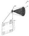
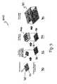
- FIG. 1shows a focal plane array imager
- FIG. 2shows imaging optics of the focal plane array imager.
- FIG. 3shows a horn antenna array according to embodiments of the invention.
- FIG. 4shows a detector module according to embodiments of the invention.
- FIG. 5shows an assembly process flow for a printed circuit board and an exploded view of the printed circuit board according to embodiments of the invention.
- FIG. 6shows the MMIC chip including a BTD detector in perspective view according to embodiments of the invention.
- FIG. 7shows the MMIC chip including the BTD detector and flip chip assembled onto the printed circuit board in plan view according to embodiments of the invention.
- FIG. 8shows the MMIC chip of FIG. 7 in perspective view.
- FIG. 9shows a low-cost assembly process for the focal plane array according to embodiments of this invention.
- FIG. 10shows the focal plane array in cross-sectional view according to embodiments of this invention.
- detectors based upon a BTD as taught in U.S. Pat. No. 6,635,907, the entire content of which is incorporated herein by reference,are integrated with a low noise antenna array and readout electronics, resulting in a low cost imager.
- a BTDis a high-speed semiconductor device that exhibits an interband tunneling characteristic. Two semiconductor regions that have different compositions from one another are separated by a thin interface layer. The two semiconductor regions have energy bands shifted in opposite directions and the interface layer is thin in order to allow for electron transfer through tunneling.
- the BTDtypically includes a heterostructure of a first layer of InAs and a second layer of GaSb or InGaSb with an interface layer of an aluminum antimonide compound. The presence of aluminum antimonide compound in the interface enhances the highly nonlinear current-voltage (I-V) curve near zero bias.
- the band gap engineering of the BTDresults in high nonlinearity in its current versus voltage characteristics right at 0V. This nonlinearity at 0V results in high responsivity at 0V. High responsivity yield a sensitive detector. Having the high nonlinearity at 0V allows the use of the BTD without having to apply a DC bias that generates a significant amount of noise. The nonlinearity characteristics of the BTD, therefore, results in a low noise sensor whose result is usable without prior RF amplification.
- RE LNAsmay reduce the sensitivity. However, this reduction in sensitivity is regained due to the ability to incorporate large numbers of pixels in a two dimensional array without generating heat.
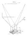
- FIG. 1shows a focal plane array imager 100 .
- the focal plane array imager 100includes an objective lens 10 that forms an image onto a focal plane array 20 .
- the focal plane array 20includes an array of pixels 200 arranged in a two-dimensional matrix.
- the lens 10may be a plano-convex lens made of a suitable dielectric material to minimize loss at millimeter wave frequencies.
- a suitable dielectric materialto minimize loss at millimeter wave frequencies.
- An example of this type of materialis Rexolite®.
- the lens 10may or may not include grooves for antireflection.
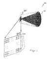
- FIG. 2shows imaging optics of the focal plane array imager 100 .
- the 3 dB beam width ⁇ 3 db of beams 15 arriving at the pixel 200 on the focal plane array 20 of FIG. 1is shown in FIG. 2 .
- the angular resolution ⁇ of the imager 100is defined as difference between the beam angle of adjacent pixels 200 .
- Focal length F or focal distance of a lensis the distance from the lens 10 to the focal plane 20 of the lens 10 where a width of a refracted group of incoming parallel rays 17 is at its narrowest or where a group of parallel rays 17 are focused by the lens 10 .
- lens 10produces a limited focal plane over which quality focusing is achieved.
- the field of view of the imageris determined by the angular resolution ⁇ times the number of pixels 200 along a row or a column.
- the diameter of the lens Dis determined by trading off image quality, physical array size, and field of view.
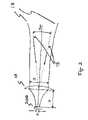
- a reflectormay be used instead of a lens.
- a parabolic reflectorprovides focusing similar to a lens, but upon reflection rather than transmission. If a reflector is used, it is common to utilize an offset-fed reflector to avoid aperture blockage by the imaging sensor, because this sensor must sit in front of the reflector. Reflectors introduce less loss than lenses because the waves need not travel through an material. In short, using a lens avoids aperture blockage while a reflector is more efficient.
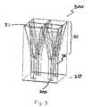
- FIG. 3shows a representative four-pixel horn antenna array 300 .
- the focal plane array 20as shown in FIG. 1 , is coupled with an array 300 of individual horn antennas 30 .
- Each horn antenna 30may end in a rectangular waveguide 35 portion as needed which in turn could be coupled to a corresponding pixel 200 .
- the horn antennas 30can be single or dual polarized with dual polarization providing an exemplary embodiment which raises imager sensitivity.
- the dual polarizationraises imager sensitivity by 1.5 dB.
- single polarizationincreases bandwidth and the imager 100 is more tolerant to misalignment of the horn antennas 30 during assembly.
- the assembly of the waveguide 35 and the pixel 200that may be achieved by a silver epoxy, is tolerant to misalignment when either the waveguide 35 or the pixel 200 are translated diagonally.
- the horn antennas 30form a diagonal feed array because their inlet rectangular cross section 31 is rotated with respect to the rectangular cross section of the corresponding pixel 200 .
- the horn antenna 30may be approximately 0.32 inches on each side of its rectangular cross section 31 and 0.62 inches in height.
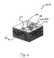
- FIG. 4shows a representative detector module 400 .
- the horn antenna array 300may be molded or cast to form a single block that is electrically connected to an RF printed circuit board (PCB) 50 .
- FIG. 4schematically shows a representative waveguide 35 coupling a portion of the PCB 50 to a representative horn antenna 30 .
- the PCB 50has a corresponding detector (not shown) associated with the representative assembly of the waveguide 35 and the horn antenna.
- a set of detector modules 400 arranged in an arrayform the focal plane array 20 of FIG. 1 . Transition from the waveguide 35 to the detector is a critical RF path that provides efficient power transfer over a wide bandwidth of frequencies and may be assembled at a low cost. The signal detected may be fed through to readout electronic circuitry.
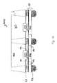
- the PCB 50includes a quartz substrate 550 that includes electrical connections 221 for readout circuitry (see FIG. 9 ) located on the bottom or back side 552 and monolithic microwave integrated circuit (MMIC) chips 220 mounted on the top or front side 551 .
- the quartz substrate 550includes vias 54 that are formed through the quartz substrate 550 wafer.
- the MMIC chips 220may be assembled onto the PCB 50 using flip chip technology.
- the detector modulemay not include the waveguide 35 and the horn antenna 30 may be directly connected to the PCB 50 .
- Connection between the horn antennas 30 and the PCB 50may be done directly, such as by bonding or through radiative coupling. Bonding can be accomplished by solder perform or silver epoxy. Radiative coupling can be achieved by maintaining the horn output openings at a fixed distance from detector coupling structures located on the PCB 50 .
- stepsare taken to ensure significant power does not radiate across the PCB 50 . This may be accomplished by using periodic etch patterns on the horn antenna array 300 bottom surface or on the PCB 50 surface that prevent power from flowing. Corrugated surfaces, for example, reflect the wave being radiated and prevent free flow of energy out of the PCB 300 .
- the quartz substrate 550may be 0.5 mm in thickness with 0.15 mm filled vias 54 .
- the vias 54serve as electrical conduction paths between the two surfaces of the quartz substrate wafer 550 if and where required.
- the vias 54also functions as antennas and contribute to the capability of the quartz substrate 550 itself to act as an antenna for oncoming wave energy.
- FIG. 5shows an assembly process flow for the PCB 50 before a MMIC chip 220 has been assembled onto it.
- the various parts of the PCB 50are shown in an exploded form.
- the front 551 or chip side metalis patterned and electroplated to form one plate 561 of an RF bypass capacitor 56 (see also FIGS. 6 and 7 ) for RF shielding and DC out regions 57 .
- Impedance matchingis done on the front side 551 , both on the MMIC chip 220 and on the PCB 50 .
- the detected outputsare routed through vias 54 from the front side 551 to the back side 552 of the PCB 50 , and from there to video amplification and other signal processing electronics. Except for the output vias 54 , the vias 54 connect the front side ground plane 551 to the back side ground plane 552 of the PCB 50 .
- the area directly beneath the MMIC chip 220does not contain vias 54 , thereby forming a back-short cavity.
- a dielectric layer 562is deposited and patterned on the chip side.
- the material deposited in this stepmay be SiN.
- the on-chip RF bypass capacitor formed using the SiN layer 562 , the capacitor plate 561 , and another capacitor plate 563 ( FIG. 6 )provides the RF bypass capacitor 56 for DC outputs.
- An RF bypass capacitoris typically a parallel element that appears as a short to RF signals and serves to carry the RF energy to ground.
- the fabrication process for the quartz substrate 550provides the transition from the E plane probes 52 to where the BTD 225 would eventually be located (not shown).
- An exemplary quartz substrate 550includes vias 54 of 2 ⁇ m height above the substrate 550 that are filled through by a mixture of W and Cu and are aligned with the DC out regions 57 .
- the fabrication processaccommodates multiple diode types including the BTD 225 that once assembled is used as the main detector of the incoming radiation.
- the “chipless” or passive RF performance of the E plane probes 52 and the quartz substrate 550 without the BTD 225may be evaluated before complete assembly of the MMIC chips 220 .
- the DC lineout 55 and the RF shielding performancemay be also evaluated during fabrication
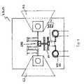
- FIG. 6shows the MMIC chip 220 in perspective view.
- This MMIC chip 220may be flipped upside down and flip chip bonded onto the PCB 50 shown in FIG. 5 .
- Au stubs or bumps 62may be electroplated on the top side of the MMIC chip 220 .
- An exemplary Au bump 62may be 20 ⁇ m-25 ⁇ m tall and 50 ⁇ m in diameter.
- the bonding of the MMIC chip 220 onto corresponding Au bumps on the surface of the quartz substrate 550may be performed by Au-Au thermo-compression.
- the MMIC chip 220includes the BTD 225 that detects the incoming wave energy and directs a corresponding signal through a meander line 64 to the RF bypass capacitor 56 having a plate 563 and to the DC out 571 of the MMIC chip 220 .
- the meander line 64gives a 90 degree phase shift to the RF bypass capacitor 56 . This creates a high RF impedance at the diode terminals of the BTD 225 , preventing the DC circuitry from interfering with the operation of the RF circuitry.
- the MMIC chip 220may be a GaAs flip chip with 0.5 ⁇ 0.5 ⁇ 0.25 mm dimensions.
- a diodemay be modeled equivalently as a series resistor Rs coupled in series to a parallel connection of a junction capacitor Cj and a junction resistor Rj.
- Exemplary parameters for a 1.5 ⁇ m ⁇ 1.5 ⁇ m BTD 225include a junction resistance Rj of 500 ⁇ , a junction capacitance Cj of 20 fF and a series resistance Rs of 13 ⁇ .
- Exemplary parameters for a 1.0 ⁇ m ⁇ 1.0 ⁇ m BTD 225include a junction resistance Rj of 1300 ⁇ , a junction capacitance Cj of 9 fF and a series resistance Rs of 28 ⁇ .
- Exemplary parameters for a 0.8 ⁇ m ⁇ 0.8 ⁇ m BTD 225include a junction resistance Rj of 2500 ⁇ , a junction capacitance Cj of 5 fF and a series resistance Rs of 40 ⁇ .
- FIG. 7shows an alternative embodiment 320 of the MMIC chip 220 as assembled upon the PCB 50 in plan view.
- the BTD 225is located between the two E plane probes 52 and is coupled to them via two portions of the circuit whose length L may be adjusted so that the effective inductance resonates with the junction capacitance of the BTD 225 . These are therefore transformer couplers between the E plane probes 52 that are electroplated on the PCB 50 and the BTD 225 that is located on the MMIC chip 320 .
- the energy detected by the BTD 225is directed through the delay or the meander line 64 to the RF bypass capacitor 56 formed from 3 layers 561 , 562 , 563 and from there to the DC out regions 57 , 571 .
- FIG. 8shows the MMIC chip of FIG. 7 in perspective view.
- FIG. 9shows a low-cost assembly process 900 for the focal plane array 20 .
- the multi-layer PCB 50is fabricated ( 90 ) with a metal pattern on the top or front side 51 that includes bonding pads for the BTD 225 and bonding pads for the horn antenna array 300 .
- Other embodimentsare possible that do not require direct bonding of the horn antenna array 300 to the PCB 50 .
- the other sidecould be called the bottom side, the output side, or the back side 53 , of the PCB 50 .
- the back side 53has bonding pads and signal lines for routing the detected signal to electronic parts located behind the PCB 50 and that are used to read the detected signal and relay it to the signal processor.
- the substrate of the PCB 50may be about a quarter wavelength electrically.
- the MMIC chip 220(or 320 ) is flip-chip bonded ( 92 ) to the front side 51 of the PCB 50 .
- Flip chip microelectronic assemblyis the direct electrical connection of face-down (hence, “flipped”) electronic components onto substrates, circuit boards, or carriers, by means of conductive bumps on the chip bond pads.
- wire bondinguses face-up chips with a wire connection to each pad.
- Flip chip componentsare predominantly semiconductor devices; however, components such as passive filters, detector arrays, and MEMs devices are also used in flip chip form.
- Flip chipis also called Direct Chip Attach because the chip is directly attached to the substrate, board, or carrier by the conductive bumps.
- Flip chiphas advantages in size, performance, flexibility, reliability, and cost over other packaging methods. Eliminating packages and bond wires reduces the required board area, and requires far less height and weight. Eliminating bond wires reduces the parasitic inductance and capacitance of the connection. The result is high speed off-chip interconnections. Flip chip gives input/output connection flexibility. Wire bond connections are limited to the perimeter of the die. Flip chip connections can use the whole area of the die, accommodating many more connections on a smaller die. Area connections also allow 3-D stacking of die and other components. Flip chip is mechanically a rugged interconnection method because flip chips, when completed with an adhesive “underfill,” are solid little blocks of cured epoxy.
- the horn antenna array 300is attached ( 94 ) to the front side 51 of the PCBs 50 over the array of BTDs 225 that are included within the MMIC chips 220 (or 320 ).
- the size of the horn antenna array 300will be determined by the tolerances required by the focal plane array 20 and the tolerances available from the manufacturing process of the horn antenna array 300 . Larger arrays can be fabricated by allowing for these tolerances and by assembling multiple horn antenna arrays 300 across the PCB 50 .
- the final assembled focal plane array 20is shown in the last step ( 96 ).
- the horn antenna array 300includes horn antennas with inlets having rectangular cross-sections.
- the rectangular cross-sections of the inlets of the horn antennas in the horn antenna array 300are shown to be parallel to the PCB ( 50 ).
- the inlet rectangular cross-section 31is shown to be parallel to focal plane array 20 and to the rectangular cross-section of the corresponding pixels 200 in the focal plane array 20 .
- FIG. 10shows an antenna array 300 assembly over a PCB 50 in cross sectional view.
- the quartz substrate 550 waferis bonded to the horn antenna 30 structure using silver epoxy or solder.
- Each MMIC chip 220 (or 320 )is flip chip bonded over the quartz substrate and is within the throat of the respective horn antenna 30 .
- Bumps or stubs 62 of the PCB 50 onto which the MMIC chip 220 (or 320 ) is bondedform orthogonal pick-up probe antennas for each horn antenna 30 for the reception of a single polarization.
- the detected output signals from the BTD 225travel along a delay line to the RF bypass capacitor 56 and then through bumps 62 to the PCB 50 .
- solder ballsmay be used to facilitate connection of the signals to subsequent amplification and signal processing.
- Ball Grid Array (BGA) 91may be used as part of the connection to subsequent amplification electronics.
- a BGAis a popular surface mount chip package that uses a grid of solder balls as its connectors. Available in plastic and ceramic varieties, BGA is noted for its compact size, high lead count and low inductance. BGA chips are easier to align to the PCB 50 , because the leads, which are called “solder balls” or “solder bumps,” are farther apart than leaded packages. Because the leads are underneath the chip, BGA has led the way to chip scale packaging (CSP) where the package is not more than 1.2 times the size of the semiconductor die itself.
- CSPchip scale packaging
- a dual polarized schemeas opposed to a single polarized scheme may be used.
- Each pixelwould require a single BTD detector for a singly polarized imager and two BTD detectors for a dual polarized imager.
- a bridge of metalmay be used so that one circuit trace may run over another without contacting it.
- the MMIC chipscan contain circuitry in addition to the BTDs that provides interconnection and impedance matching. As stated above, the MMIC chips can be mounted to a PCB using a variety of methods, such as flip chip or die attach and the circuitry on the PCB electrically connects, directly or radiatively, the BTD detectors to the horn antenna inputs.
- the outputsmay be connected to low frequency circuitry for signal conditioning, such as low noise amplifiers and Dicke switches that are used as a calibrated noise source at lower frequencies.
- low frequency circuitry for signal conditioningsuch as low noise amplifiers and Dicke switches that are used as a calibrated noise source at lower frequencies.
- Thiscan be conveniently accomplished by feeding the detected signals through the PCB to the opposite side using for example plated through holes, or vias, and connecting to the low frequency electronics that is located on the bottom side of the PCB. In this way the assembly becomes a fully integrated focal plane array.
- the PCBmay have readout electronics on the bottom or back side and flip chip MMIC chips on the top or front side where the BTDs are located.
- the entire assemblymay behave like an antenna.
- a horn antennamay be placed over the assembly of the BTD on the flip chip MMIC and on the PCB. Radiation enters the horn antenna and reaches the flip chip MMIC which is also an antenna and detects the radiation.
- Flip chipshave bumps on the back side and the bumps have catch pads on them. The flip chip metal tapers down to a spot where the BTD is located. Interconnect lines go from bump to bump and the DC output is conducted off the flip chips.
- the back side of the PCB and the interconnectsall behave as a collective antenna.
- a modular array conceptis used.
- the PCB substrateincluding the flip chip and the horn antennas that are silver epoxied onto the substrate, solder bumps on the back of the PCB connect the module to other circuitry.
- the assembly of the PCB, the flip chip MMIC and the horn antennasbecomes a module, like module shown in FIG. 4 , that can be interconnected with other modules.
- the PCB surface or the horn antenna bottom surfacemay be corrugated in order to prevent the wave from propagating through and to make it reflect back.
- the BTD detectorAs a result of the unique properties of the BTD detector, full two dimensional focal arrays can be fabricated and integrated with antenna arrays without the need for RF LNAs, unlocking the commercial and military potential of millimeter wave imaging.
- the BTDis easy to manufacture with high yields, is relatively temperature independent, exhibits low added noise, and has high responsivity.
- BTD detectorsdo not require a DC bias current to operate, so the added noise level is very low, and the BTD is only limited by thermal noise generated within the diodes. Because the diode noise is low, RF LNAs can be eliminated from the circuit, or they can be included only to further increase the sensitivity. Because of the low noise level, calibrated noise source Dicke switches do not need to be implemented at RF frequencies, but can be instead implemented at low frequencies following detection. The elimination of these RF integrated circuits significantly reduces the imager cost. This cost reduction is a direct result of the unique characteristics of the BTD detectors.
- the RF LNAis often itself a large source of noise due to drift and heat resulting from the bias current. Therefore, eliminating the RF LNA improves performance and simplifies calibration.
- a low cost array of antennassuch as the horn antennas shown in the drawings, efficiently collects RF energy and delivers that energy to the BTD detectors with minimal losses. Using the antenna array also helps reduce added noise and results in a low cost, integrated focal plane array for room temperature millimeter wave imaging.
Landscapes
- Engineering & Computer Science (AREA)
- Remote Sensing (AREA)
- Radar, Positioning & Navigation (AREA)
- Physics & Mathematics (AREA)
- Electromagnetism (AREA)
- Computer Networks & Wireless Communication (AREA)
- General Physics & Mathematics (AREA)
- Microelectronics & Electronic Packaging (AREA)
- Radar Systems Or Details Thereof (AREA)
- Variable-Direction Aerials And Aerial Arrays (AREA)
Abstract
Description
Claims (10)
Priority Applications (2)
| Application Number | Priority Date | Filing Date | Title |
|---|---|---|---|
| US11/303,642US7583074B1 (en) | 2005-12-16 | 2005-12-16 | Low cost millimeter wave imager |
| US12/503,690US7795859B1 (en) | 2005-12-16 | 2009-07-15 | Low cost millimeter wave imager |
Applications Claiming Priority (1)
| Application Number | Priority Date | Filing Date | Title |
|---|---|---|---|
| US11/303,642US7583074B1 (en) | 2005-12-16 | 2005-12-16 | Low cost millimeter wave imager |
Related Child Applications (1)
| Application Number | Title | Priority Date | Filing Date |
|---|---|---|---|
| US12/503,690DivisionUS7795859B1 (en) | 2005-12-16 | 2009-07-15 | Low cost millimeter wave imager |
Publications (1)
| Publication Number | Publication Date |
|---|---|
| US7583074B1true US7583074B1 (en) | 2009-09-01 |
Family
ID=41009196
Family Applications (2)
| Application Number | Title | Priority Date | Filing Date |
|---|---|---|---|
| US11/303,642Expired - Fee RelatedUS7583074B1 (en) | 2005-12-16 | 2005-12-16 | Low cost millimeter wave imager |
| US12/503,690Expired - Fee RelatedUS7795859B1 (en) | 2005-12-16 | 2009-07-15 | Low cost millimeter wave imager |
Family Applications After (1)
| Application Number | Title | Priority Date | Filing Date |
|---|---|---|---|
| US12/503,690Expired - Fee RelatedUS7795859B1 (en) | 2005-12-16 | 2009-07-15 | Low cost millimeter wave imager |
Country Status (1)
| Country | Link |
|---|---|
| US (2) | US7583074B1 (en) |
Cited By (180)
| Publication number | Priority date | Publication date | Assignee | Title |
|---|---|---|---|---|
| US20070262879A1 (en)* | 2006-05-12 | 2007-11-15 | Robert Greiner | I/O bus for analog sensors in an IC |
| US7795859B1 (en)* | 2005-12-16 | 2010-09-14 | Hrl Laboratories, Llc | Low cost millimeter wave imager |
| US20100301217A1 (en)* | 2009-05-28 | 2010-12-02 | The Ohio State University | MINIATURE PHASE-CORRECTED ANTENNAS FOR HIGH RESOLUTION FOCAL PLANE THz IMAGING ARRAYS |
| US8080774B1 (en)* | 2008-08-12 | 2011-12-20 | Hrl Laboratories, Llc | Module for scalable millimeter wave imaging arrays |
| US20120085909A1 (en)* | 2010-06-30 | 2012-04-12 | Nuctech Company Limited | Millimeter-wave inspection apparatus |
| US20120255763A1 (en)* | 2011-04-06 | 2012-10-11 | Dong-Hyun Baek | Card-type information recording medium having embedded antenna for near field communication and manufacturing method thereof |
| US8390403B1 (en) | 2009-01-26 | 2013-03-05 | Hrl Laboratories, Llc | Wideband ridged waveguide to diode detector transition |
| US20130187721A1 (en)* | 2012-01-19 | 2013-07-25 | Canon Kabushiki Kaisha | Oscillation element, oscillator, and imaging apparatus using the same |
| CN104051836A (en)* | 2014-06-10 | 2014-09-17 | 首都师范大学 | A terahertz waveguide coupler |
| US9119127B1 (en) | 2012-12-05 | 2015-08-25 | At&T Intellectual Property I, Lp | Backhaul link for distributed antenna system |
| US9154966B2 (en) | 2013-11-06 | 2015-10-06 | At&T Intellectual Property I, Lp | Surface-wave communications and methods thereof |
| US9209902B2 (en) | 2013-12-10 | 2015-12-08 | At&T Intellectual Property I, L.P. | Quasi-optical coupler |
| US9312919B1 (en) | 2014-10-21 | 2016-04-12 | At&T Intellectual Property I, Lp | Transmission device with impairment compensation and methods for use therewith |
| US9461706B1 (en) | 2015-07-31 | 2016-10-04 | At&T Intellectual Property I, Lp | Method and apparatus for exchanging communication signals |
| US9490869B1 (en) | 2015-05-14 | 2016-11-08 | At&T Intellectual Property I, L.P. | Transmission medium having multiple cores and methods for use therewith |
| US9503189B2 (en) | 2014-10-10 | 2016-11-22 | At&T Intellectual Property I, L.P. | Method and apparatus for arranging communication sessions in a communication system |
| US9509415B1 (en) | 2015-06-25 | 2016-11-29 | At&T Intellectual Property I, L.P. | Methods and apparatus for inducing a fundamental wave mode on a transmission medium |
| US9520945B2 (en) | 2014-10-21 | 2016-12-13 | At&T Intellectual Property I, L.P. | Apparatus for providing communication services and methods thereof |
| US9525524B2 (en) | 2013-05-31 | 2016-12-20 | At&T Intellectual Property I, L.P. | Remote distributed antenna system |
| US9525210B2 (en) | 2014-10-21 | 2016-12-20 | At&T Intellectual Property I, L.P. | Guided-wave transmission device with non-fundamental mode propagation and methods for use therewith |
| US9531427B2 (en) | 2014-11-20 | 2016-12-27 | At&T Intellectual Property I, L.P. | Transmission device with mode division multiplexing and methods for use therewith |
| US9564947B2 (en) | 2014-10-21 | 2017-02-07 | At&T Intellectual Property I, L.P. | Guided-wave transmission device with diversity and methods for use therewith |
| US9577307B2 (en) | 2014-10-21 | 2017-02-21 | At&T Intellectual Property I, L.P. | Guided-wave transmission device and methods for use therewith |
| US9608692B2 (en) | 2015-06-11 | 2017-03-28 | At&T Intellectual Property I, L.P. | Repeater and methods for use therewith |
| US9608740B2 (en) | 2015-07-15 | 2017-03-28 | At&T Intellectual Property I, L.P. | Method and apparatus for launching a wave mode that mitigates interference |
| US9615269B2 (en) | 2014-10-02 | 2017-04-04 | At&T Intellectual Property I, L.P. | Method and apparatus that provides fault tolerance in a communication network |
| US9628854B2 (en) | 2014-09-29 | 2017-04-18 | At&T Intellectual Property I, L.P. | Method and apparatus for distributing content in a communication network |
| US9628116B2 (en) | 2015-07-14 | 2017-04-18 | At&T Intellectual Property I, L.P. | Apparatus and methods for transmitting wireless signals |
| US9640850B2 (en) | 2015-06-25 | 2017-05-02 | At&T Intellectual Property I, L.P. | Methods and apparatus for inducing a non-fundamental wave mode on a transmission medium |
| US9653770B2 (en) | 2014-10-21 | 2017-05-16 | At&T Intellectual Property I, L.P. | Guided wave coupler, coupling module and methods for use therewith |
| US9654173B2 (en) | 2014-11-20 | 2017-05-16 | At&T Intellectual Property I, L.P. | Apparatus for powering a communication device and methods thereof |
| US9667317B2 (en) | 2015-06-15 | 2017-05-30 | At&T Intellectual Property I, L.P. | Method and apparatus for providing security using network traffic adjustments |
| US9680670B2 (en) | 2014-11-20 | 2017-06-13 | At&T Intellectual Property I, L.P. | Transmission device with channel equalization and control and methods for use therewith |
| US9685992B2 (en) | 2014-10-03 | 2017-06-20 | At&T Intellectual Property I, L.P. | Circuit panel network and methods thereof |
| US9692101B2 (en) | 2014-08-26 | 2017-06-27 | At&T Intellectual Property I, L.P. | Guided wave couplers for coupling electromagnetic waves between a waveguide surface and a surface of a wire |
| US9705571B2 (en) | 2015-09-16 | 2017-07-11 | At&T Intellectual Property I, L.P. | Method and apparatus for use with a radio distributed antenna system |
| US9705561B2 (en) | 2015-04-24 | 2017-07-11 | At&T Intellectual Property I, L.P. | Directional coupling device and methods for use therewith |
| US9722316B2 (en) | 2014-07-07 | 2017-08-01 | Google Inc. | Horn lens antenna |
| US9722318B2 (en) | 2015-07-14 | 2017-08-01 | At&T Intellectual Property I, L.P. | Method and apparatus for coupling an antenna to a device |
| US9729197B2 (en) | 2015-10-01 | 2017-08-08 | At&T Intellectual Property I, L.P. | Method and apparatus for communicating network management traffic over a network |
| US9735833B2 (en) | 2015-07-31 | 2017-08-15 | At&T Intellectual Property I, L.P. | Method and apparatus for communications management in a neighborhood network |
| US9742462B2 (en) | 2014-12-04 | 2017-08-22 | At&T Intellectual Property I, L.P. | Transmission medium and communication interfaces and methods for use therewith |
| US9749053B2 (en) | 2015-07-23 | 2017-08-29 | At&T Intellectual Property I, L.P. | Node device, repeater and methods for use therewith |
| US9749013B2 (en) | 2015-03-17 | 2017-08-29 | At&T Intellectual Property I, L.P. | Method and apparatus for reducing attenuation of electromagnetic waves guided by a transmission medium |
| US9748626B2 (en) | 2015-05-14 | 2017-08-29 | At&T Intellectual Property I, L.P. | Plurality of cables having different cross-sectional shapes which are bundled together to form a transmission medium |
| US9755697B2 (en) | 2014-09-15 | 2017-09-05 | At&T Intellectual Property I, L.P. | Method and apparatus for sensing a condition in a transmission medium of electromagnetic waves |
| US9762289B2 (en) | 2014-10-14 | 2017-09-12 | At&T Intellectual Property I, L.P. | Method and apparatus for transmitting or receiving signals in a transportation system |
| US9769020B2 (en) | 2014-10-21 | 2017-09-19 | At&T Intellectual Property I, L.P. | Method and apparatus for responding to events affecting communications in a communication network |
| US9769128B2 (en) | 2015-09-28 | 2017-09-19 | At&T Intellectual Property I, L.P. | Method and apparatus for encryption of communications over a network |
| US9774076B2 (en) | 2010-08-31 | 2017-09-26 | Siklu Communication ltd. | Compact millimeter-wave radio systems and methods |
| US9780834B2 (en) | 2014-10-21 | 2017-10-03 | At&T Intellectual Property I, L.P. | Method and apparatus for transmitting electromagnetic waves |
| US9793951B2 (en) | 2015-07-15 | 2017-10-17 | At&T Intellectual Property I, L.P. | Method and apparatus for launching a wave mode that mitigates interference |
| US9793954B2 (en) | 2015-04-28 | 2017-10-17 | At&T Intellectual Property I, L.P. | Magnetic coupling device and methods for use therewith |
| US9793955B2 (en) | 2015-04-24 | 2017-10-17 | At&T Intellectual Property I, Lp | Passive electrical coupling device and methods for use therewith |
| US9800327B2 (en) | 2014-11-20 | 2017-10-24 | At&T Intellectual Property I, L.P. | Apparatus for controlling operations of a communication device and methods thereof |
| US9820146B2 (en) | 2015-06-12 | 2017-11-14 | At&T Intellectual Property I, L.P. | Method and apparatus for authentication and identity management of communicating devices |
| US9836957B2 (en) | 2015-07-14 | 2017-12-05 | At&T Intellectual Property I, L.P. | Method and apparatus for communicating with premises equipment |
| US9838896B1 (en) | 2016-12-09 | 2017-12-05 | At&T Intellectual Property I, L.P. | Method and apparatus for assessing network coverage |
| US9847850B2 (en) | 2014-10-14 | 2017-12-19 | At&T Intellectual Property I, L.P. | Method and apparatus for adjusting a mode of communication in a communication network |
| US9847566B2 (en) | 2015-07-14 | 2017-12-19 | At&T Intellectual Property I, L.P. | Method and apparatus for adjusting a field of a signal to mitigate interference |
| US9853342B2 (en) | 2015-07-14 | 2017-12-26 | At&T Intellectual Property I, L.P. | Dielectric transmission medium connector and methods for use therewith |
| US20170373749A1 (en)* | 2016-04-06 | 2017-12-28 | Cable Television Laboratories, Inc | Systems and methods for line attenuation testing |
| US9860075B1 (en) | 2016-08-26 | 2018-01-02 | At&T Intellectual Property I, L.P. | Method and communication node for broadband distribution |
| US9865911B2 (en) | 2015-06-25 | 2018-01-09 | At&T Intellectual Property I, L.P. | Waveguide system for slot radiating first electromagnetic waves that are combined into a non-fundamental wave mode second electromagnetic wave on a transmission medium |
| US9866309B2 (en) | 2015-06-03 | 2018-01-09 | At&T Intellectual Property I, Lp | Host node device and methods for use therewith |
| US9871283B2 (en) | 2015-07-23 | 2018-01-16 | At&T Intellectual Property I, Lp | Transmission medium having a dielectric core comprised of plural members connected by a ball and socket configuration |
| US9871282B2 (en) | 2015-05-14 | 2018-01-16 | At&T Intellectual Property I, L.P. | At least one transmission medium having a dielectric surface that is covered at least in part by a second dielectric |
| US9876605B1 (en) | 2016-10-21 | 2018-01-23 | At&T Intellectual Property I, L.P. | Launcher and coupling system to support desired guided wave mode |
| US9876264B2 (en) | 2015-10-02 | 2018-01-23 | At&T Intellectual Property I, Lp | Communication system, guided wave switch and methods for use therewith |
| US9876571B2 (en) | 2015-02-20 | 2018-01-23 | At&T Intellectual Property I, Lp | Guided-wave transmission device with non-fundamental mode propagation and methods for use therewith |
| US9882277B2 (en) | 2015-10-02 | 2018-01-30 | At&T Intellectual Property I, Lp | Communication device and antenna assembly with actuated gimbal mount |
| US9882257B2 (en) | 2015-07-14 | 2018-01-30 | At&T Intellectual Property I, L.P. | Method and apparatus for launching a wave mode that mitigates interference |
| US9893795B1 (en) | 2016-12-07 | 2018-02-13 | At&T Intellectual Property I, Lp | Method and repeater for broadband distribution |
| US9906269B2 (en) | 2014-09-17 | 2018-02-27 | At&T Intellectual Property I, L.P. | Monitoring and mitigating conditions in a communication network |
| US9904535B2 (en) | 2015-09-14 | 2018-02-27 | At&T Intellectual Property I, L.P. | Method and apparatus for distributing software |
| US9913139B2 (en) | 2015-06-09 | 2018-03-06 | At&T Intellectual Property I, L.P. | Signal fingerprinting for authentication of communicating devices |
| US9911020B1 (en) | 2016-12-08 | 2018-03-06 | At&T Intellectual Property I, L.P. | Method and apparatus for tracking via a radio frequency identification device |
| US9912419B1 (en) | 2016-08-24 | 2018-03-06 | At&T Intellectual Property I, L.P. | Method and apparatus for managing a fault in a distributed antenna system |
| US9912381B2 (en) | 2015-06-03 | 2018-03-06 | At&T Intellectual Property I, Lp | Network termination and methods for use therewith |
| US9912027B2 (en) | 2015-07-23 | 2018-03-06 | At&T Intellectual Property I, L.P. | Method and apparatus for exchanging communication signals |
| US9917341B2 (en) | 2015-05-27 | 2018-03-13 | At&T Intellectual Property I, L.P. | Apparatus and method for launching electromagnetic waves and for modifying radial dimensions of the propagating electromagnetic waves |
| US9927517B1 (en) | 2016-12-06 | 2018-03-27 | At&T Intellectual Property I, L.P. | Apparatus and methods for sensing rainfall |
| US9948333B2 (en) | 2015-07-23 | 2018-04-17 | At&T Intellectual Property I, L.P. | Method and apparatus for wireless communications to mitigate interference |
| US9948354B2 (en) | 2015-04-28 | 2018-04-17 | At&T Intellectual Property I, L.P. | Magnetic coupling device with reflective plate and methods for use therewith |
| US9954287B2 (en) | 2014-11-20 | 2018-04-24 | At&T Intellectual Property I, L.P. | Apparatus for converting wireless signals and electromagnetic waves and methods thereof |
| US9967173B2 (en) | 2015-07-31 | 2018-05-08 | At&T Intellectual Property I, L.P. | Method and apparatus for authentication and identity management of communicating devices |
| US9973940B1 (en) | 2017-02-27 | 2018-05-15 | At&T Intellectual Property I, L.P. | Apparatus and methods for dynamic impedance matching of a guided wave launcher |
| US9991580B2 (en) | 2016-10-21 | 2018-06-05 | At&T Intellectual Property I, L.P. | Launcher and coupling system for guided wave mode cancellation |
| US9997819B2 (en) | 2015-06-09 | 2018-06-12 | At&T Intellectual Property I, L.P. | Transmission medium and method for facilitating propagation of electromagnetic waves via a core |
| US9999038B2 (en) | 2013-05-31 | 2018-06-12 | At&T Intellectual Property I, L.P. | Remote distributed antenna system |
| US9998870B1 (en) | 2016-12-08 | 2018-06-12 | At&T Intellectual Property I, L.P. | Method and apparatus for proximity sensing |
| US10009063B2 (en) | 2015-09-16 | 2018-06-26 | At&T Intellectual Property I, L.P. | Method and apparatus for use with a radio distributed antenna system having an out-of-band reference signal |
| US10009901B2 (en) | 2015-09-16 | 2018-06-26 | At&T Intellectual Property I, L.P. | Method, apparatus, and computer-readable storage medium for managing utilization of wireless resources between base stations |
| US10009067B2 (en) | 2014-12-04 | 2018-06-26 | At&T Intellectual Property I, L.P. | Method and apparatus for configuring a communication interface |
| US10009065B2 (en) | 2012-12-05 | 2018-06-26 | At&T Intellectual Property I, L.P. | Backhaul link for distributed antenna system |
| US10020844B2 (en) | 2016-12-06 | 2018-07-10 | T&T Intellectual Property I, L.P. | Method and apparatus for broadcast communication via guided waves |
| US10020587B2 (en) | 2015-07-31 | 2018-07-10 | At&T Intellectual Property I, L.P. | Radial antenna and methods for use therewith |
| US10027397B2 (en) | 2016-12-07 | 2018-07-17 | At&T Intellectual Property I, L.P. | Distributed antenna system and methods for use therewith |
| US10033108B2 (en) | 2015-07-14 | 2018-07-24 | At&T Intellectual Property I, L.P. | Apparatus and methods for generating an electromagnetic wave having a wave mode that mitigates interference |
| US10033107B2 (en) | 2015-07-14 | 2018-07-24 | At&T Intellectual Property I, L.P. | Method and apparatus for coupling an antenna to a device |
| US10044409B2 (en) | 2015-07-14 | 2018-08-07 | At&T Intellectual Property I, L.P. | Transmission medium and methods for use therewith |
| US10051483B2 (en) | 2015-10-16 | 2018-08-14 | At&T Intellectual Property I, L.P. | Method and apparatus for directing wireless signals |
| US10051629B2 (en) | 2015-09-16 | 2018-08-14 | At&T Intellectual Property I, L.P. | Method and apparatus for use with a radio distributed antenna system having an in-band reference signal |
| US10069535B2 (en) | 2016-12-08 | 2018-09-04 | At&T Intellectual Property I, L.P. | Apparatus and methods for launching electromagnetic waves having a certain electric field structure |
| US10074890B2 (en) | 2015-10-02 | 2018-09-11 | At&T Intellectual Property I, L.P. | Communication device and antenna with integrated light assembly |
| US10079661B2 (en) | 2015-09-16 | 2018-09-18 | At&T Intellectual Property I, L.P. | Method and apparatus for use with a radio distributed antenna system having a clock reference |
| US10090606B2 (en) | 2015-07-15 | 2018-10-02 | At&T Intellectual Property I, L.P. | Antenna system with dielectric array and methods for use therewith |
| US10090594B2 (en) | 2016-11-23 | 2018-10-02 | At&T Intellectual Property I, L.P. | Antenna system having structural configurations for assembly |
| US10103801B2 (en) | 2015-06-03 | 2018-10-16 | At&T Intellectual Property I, L.P. | Host node device and methods for use therewith |
| US10103422B2 (en) | 2016-12-08 | 2018-10-16 | At&T Intellectual Property I, L.P. | Method and apparatus for mounting network devices |
| US10136434B2 (en) | 2015-09-16 | 2018-11-20 | At&T Intellectual Property I, L.P. | Method and apparatus for use with a radio distributed antenna system having an ultra-wideband control channel |
| US10135145B2 (en) | 2016-12-06 | 2018-11-20 | At&T Intellectual Property I, L.P. | Apparatus and methods for generating an electromagnetic wave along a transmission medium |
| US10135146B2 (en) | 2016-10-18 | 2018-11-20 | At&T Intellectual Property I, L.P. | Apparatus and methods for launching guided waves via circuits |
| US10135147B2 (en) | 2016-10-18 | 2018-11-20 | At&T Intellectual Property I, L.P. | Apparatus and methods for launching guided waves via an antenna |
| US10139820B2 (en) | 2016-12-07 | 2018-11-27 | At&T Intellectual Property I, L.P. | Method and apparatus for deploying equipment of a communication system |
| US10142086B2 (en) | 2015-06-11 | 2018-11-27 | At&T Intellectual Property I, L.P. | Repeater and methods for use therewith |
| US10144036B2 (en) | 2015-01-30 | 2018-12-04 | At&T Intellectual Property I, L.P. | Method and apparatus for mitigating interference affecting a propagation of electromagnetic waves guided by a transmission medium |
| US10148016B2 (en) | 2015-07-14 | 2018-12-04 | At&T Intellectual Property I, L.P. | Apparatus and methods for communicating utilizing an antenna array |
| US10154493B2 (en) | 2015-06-03 | 2018-12-11 | At&T Intellectual Property I, L.P. | Network termination and methods for use therewith |
| US10168695B2 (en) | 2016-12-07 | 2019-01-01 | At&T Intellectual Property I, L.P. | Method and apparatus for controlling an unmanned aircraft |
| US10170840B2 (en) | 2015-07-14 | 2019-01-01 | At&T Intellectual Property I, L.P. | Apparatus and methods for sending or receiving electromagnetic signals |
| US10178445B2 (en) | 2016-11-23 | 2019-01-08 | At&T Intellectual Property I, L.P. | Methods, devices, and systems for load balancing between a plurality of waveguides |
| US10205655B2 (en) | 2015-07-14 | 2019-02-12 | At&T Intellectual Property I, L.P. | Apparatus and methods for communicating utilizing an antenna array and multiple communication paths |
| US10225025B2 (en) | 2016-11-03 | 2019-03-05 | At&T Intellectual Property I, L.P. | Method and apparatus for detecting a fault in a communication system |
| US10224363B2 (en)* | 2016-07-28 | 2019-03-05 | Neteera Technologies Ltd. | Terahertz CMOS sensor |
| US10224634B2 (en) | 2016-11-03 | 2019-03-05 | At&T Intellectual Property I, L.P. | Methods and apparatus for adjusting an operational characteristic of an antenna |
| US10243270B2 (en) | 2016-12-07 | 2019-03-26 | At&T Intellectual Property I, L.P. | Beam adaptive multi-feed dielectric antenna system and methods for use therewith |
| US10243784B2 (en) | 2014-11-20 | 2019-03-26 | At&T Intellectual Property I, L.P. | System for generating topology information and methods thereof |
| US10264586B2 (en) | 2016-12-09 | 2019-04-16 | At&T Mobility Ii Llc | Cloud-based packet controller and methods for use therewith |
| US10291311B2 (en) | 2016-09-09 | 2019-05-14 | At&T Intellectual Property I, L.P. | Method and apparatus for mitigating a fault in a distributed antenna system |
| US10291334B2 (en) | 2016-11-03 | 2019-05-14 | At&T Intellectual Property I, L.P. | System for detecting a fault in a communication system |
| US10298293B2 (en) | 2017-03-13 | 2019-05-21 | At&T Intellectual Property I, L.P. | Apparatus of communication utilizing wireless network devices |
| US10305190B2 (en) | 2016-12-01 | 2019-05-28 | At&T Intellectual Property I, L.P. | Reflecting dielectric antenna system and methods for use therewith |
| US10312567B2 (en) | 2016-10-26 | 2019-06-04 | At&T Intellectual Property I, L.P. | Launcher with planar strip antenna and methods for use therewith |
| US10320586B2 (en) | 2015-07-14 | 2019-06-11 | At&T Intellectual Property I, L.P. | Apparatus and methods for generating non-interfering electromagnetic waves on an insulated transmission medium |
| US10326689B2 (en) | 2016-12-08 | 2019-06-18 | At&T Intellectual Property I, L.P. | Method and system for providing alternative communication paths |
| US10326494B2 (en) | 2016-12-06 | 2019-06-18 | At&T Intellectual Property I, L.P. | Apparatus for measurement de-embedding and methods for use therewith |
| US10340600B2 (en) | 2016-10-18 | 2019-07-02 | At&T Intellectual Property I, L.P. | Apparatus and methods for launching guided waves via plural waveguide systems |
| US10340601B2 (en) | 2016-11-23 | 2019-07-02 | At&T Intellectual Property I, L.P. | Multi-antenna system and methods for use therewith |
| US10340983B2 (en) | 2016-12-09 | 2019-07-02 | At&T Intellectual Property I, L.P. | Method and apparatus for surveying remote sites via guided wave communications |
| US10340603B2 (en) | 2016-11-23 | 2019-07-02 | At&T Intellectual Property I, L.P. | Antenna system having shielded structural configurations for assembly |
| US10341142B2 (en) | 2015-07-14 | 2019-07-02 | At&T Intellectual Property I, L.P. | Apparatus and methods for generating non-interfering electromagnetic waves on an uninsulated conductor |
| US10340573B2 (en) | 2016-10-26 | 2019-07-02 | At&T Intellectual Property I, L.P. | Launcher with cylindrical coupling device and methods for use therewith |
| US10348391B2 (en) | 2015-06-03 | 2019-07-09 | At&T Intellectual Property I, L.P. | Client node device with frequency conversion and methods for use therewith |
| US10355367B2 (en) | 2015-10-16 | 2019-07-16 | At&T Intellectual Property I, L.P. | Antenna structure for exchanging wireless signals |
| US10361489B2 (en) | 2016-12-01 | 2019-07-23 | At&T Intellectual Property I, L.P. | Dielectric dish antenna system and methods for use therewith |
| US10359749B2 (en) | 2016-12-07 | 2019-07-23 | At&T Intellectual Property I, L.P. | Method and apparatus for utilities management via guided wave communication |
| US10374316B2 (en) | 2016-10-21 | 2019-08-06 | At&T Intellectual Property I, L.P. | System and dielectric antenna with non-uniform dielectric |
| US10382976B2 (en) | 2016-12-06 | 2019-08-13 | At&T Intellectual Property I, L.P. | Method and apparatus for managing wireless communications based on communication paths and network device positions |
| US10389029B2 (en) | 2016-12-07 | 2019-08-20 | At&T Intellectual Property I, L.P. | Multi-feed dielectric antenna system with core selection and methods for use therewith |
| US10389037B2 (en) | 2016-12-08 | 2019-08-20 | At&T Intellectual Property I, L.P. | Apparatus and methods for selecting sections of an antenna array and use therewith |
| US10396887B2 (en) | 2015-06-03 | 2019-08-27 | At&T Intellectual Property I, L.P. | Client node device and methods for use therewith |
| US10411356B2 (en) | 2016-12-08 | 2019-09-10 | At&T Intellectual Property I, L.P. | Apparatus and methods for selectively targeting communication devices with an antenna array |
| US10439675B2 (en) | 2016-12-06 | 2019-10-08 | At&T Intellectual Property I, L.P. | Method and apparatus for repeating guided wave communication signals |
| US10446936B2 (en) | 2016-12-07 | 2019-10-15 | At&T Intellectual Property I, L.P. | Multi-feed dielectric antenna system and methods for use therewith |
| US10498044B2 (en) | 2016-11-03 | 2019-12-03 | At&T Intellectual Property I, L.P. | Apparatus for configuring a surface of an antenna |
| US10530505B2 (en) | 2016-12-08 | 2020-01-07 | At&T Intellectual Property I, L.P. | Apparatus and methods for launching electromagnetic waves along a transmission medium |
| US10535928B2 (en) | 2016-11-23 | 2020-01-14 | At&T Intellectual Property I, L.P. | Antenna system and methods for use therewith |
| US10547348B2 (en) | 2016-12-07 | 2020-01-28 | At&T Intellectual Property I, L.P. | Method and apparatus for switching transmission mediums in a communication system |
| US10601494B2 (en) | 2016-12-08 | 2020-03-24 | At&T Intellectual Property I, L.P. | Dual-band communication device and method for use therewith |
| US10637149B2 (en) | 2016-12-06 | 2020-04-28 | At&T Intellectual Property I, L.P. | Injection molded dielectric antenna and methods for use therewith |
| US10650940B2 (en) | 2015-05-15 | 2020-05-12 | At&T Intellectual Property I, L.P. | Transmission medium having a conductive material and methods for use therewith |
| US10665942B2 (en) | 2015-10-16 | 2020-05-26 | At&T Intellectual Property I, L.P. | Method and apparatus for adjusting wireless communications |
| US10680708B2 (en) | 2016-04-06 | 2020-06-09 | Cable Television Laboratories, Inc | Systems and methods for locating a single reflection on a transmission line |
| US10679767B2 (en) | 2015-05-15 | 2020-06-09 | At&T Intellectual Property I, L.P. | Transmission medium having a conductive material and methods for use therewith |
| US10694379B2 (en) | 2016-12-06 | 2020-06-23 | At&T Intellectual Property I, L.P. | Waveguide system with device-based authentication and methods for use therewith |
| US10727599B2 (en) | 2016-12-06 | 2020-07-28 | At&T Intellectual Property I, L.P. | Launcher with slot antenna and methods for use therewith |
| US10755542B2 (en) | 2016-12-06 | 2020-08-25 | At&T Intellectual Property I, L.P. | Method and apparatus for surveillance via guided wave communication |
| US10777873B2 (en) | 2016-12-08 | 2020-09-15 | At&T Intellectual Property I, L.P. | Method and apparatus for mounting network devices |
| US10784670B2 (en) | 2015-07-23 | 2020-09-22 | At&T Intellectual Property I, L.P. | Antenna support for aligning an antenna |
| US10811767B2 (en) | 2016-10-21 | 2020-10-20 | At&T Intellectual Property I, L.P. | System and dielectric antenna with convex dielectric radome |
| US10819035B2 (en) | 2016-12-06 | 2020-10-27 | At&T Intellectual Property I, L.P. | Launcher with helical antenna and methods for use therewith |
| US10916969B2 (en) | 2016-12-08 | 2021-02-09 | At&T Intellectual Property I, L.P. | Method and apparatus for providing power using an inductive coupling |
| US10938108B2 (en) | 2016-12-08 | 2021-03-02 | At&T Intellectual Property I, L.P. | Frequency selective multi-feed dielectric antenna system and methods for use therewith |
| US11032819B2 (en) | 2016-09-15 | 2021-06-08 | At&T Intellectual Property I, L.P. | Method and apparatus for use with a radio distributed antenna system having a control channel reference signal |
| EP3845930A1 (en)* | 2019-12-30 | 2021-07-07 | Tsinghua University | Passive security checking device and receiving antenna unit thereof |
| US11199608B2 (en)* | 2016-10-04 | 2021-12-14 | Hitachi Automotive Systems, Ltd. | Antenna, sensor, and vehicle mounted system |
| US11387547B2 (en)* | 2017-06-05 | 2022-07-12 | Hitachi Astemo, Ltd. | Antenna, array antenna, radar apparatus, and in-vehicle system |
| CN115266326A (en)* | 2022-06-13 | 2022-11-01 | 东南大学 | A kind of in-situ detection device and measurement method of composite material damage based on millimeter wave |
| EP4386981A1 (en)* | 2022-12-14 | 2024-06-19 | Bitsensing Inc. | Waveguide antenna and radar apparatus including the same |
Families Citing this family (8)
| Publication number | Priority date | Publication date | Assignee | Title |
|---|---|---|---|---|
| US8791851B2 (en)* | 2011-06-02 | 2014-07-29 | International Business Machines Corporation | Hybrid millimeter wave imaging system |
| US8653467B2 (en)* | 2012-06-19 | 2014-02-18 | Raytheon Company | Multichip packaging for imaging system |
| US8934021B2 (en)* | 2012-07-02 | 2015-01-13 | Dayton D. Eden | Dual-mode terahertz imaging systems |
| US9413469B2 (en)* | 2012-07-02 | 2016-08-09 | Dayton D. Eden | Apparatus and method supporting covert communications using terahertz imaging camera |
| US11525735B2 (en) | 2016-01-11 | 2022-12-13 | Carrier Corporation | Infrared presence detector system |
| EP3403063B1 (en) | 2016-01-11 | 2023-08-30 | Carrier Corporation | Pyroelectric detector system |
| US11057072B2 (en)* | 2019-04-26 | 2021-07-06 | Battelle Memorial Institute | Systems and methods for signal communication with scalable, modular network nodes |
| US11901930B1 (en) | 2023-04-26 | 2024-02-13 | Battelle Memorial Institute | Radio frequency aperture with cooling assembly |
Citations (19)
| Publication number | Priority date | Publication date | Assignee | Title |
|---|---|---|---|---|
| US3262029A (en)* | 1962-07-24 | 1966-07-19 | Hughes Aircraft Co | Low noise microwave diode |
| US3668554A (en)* | 1971-03-29 | 1972-06-06 | Hewlett Packard Co | Yig-tuned solid state microwave oscillator |
| US3670328A (en)* | 1968-11-29 | 1972-06-13 | American Nucleonics Corp | Tunnel diode movement detector |
| US3824593A (en)* | 1972-12-04 | 1974-07-16 | Hughes Aircraft Co | Millimeter wave imaging system using direct carrier injection |
| US3882396A (en)* | 1973-08-10 | 1975-05-06 | Bell Telephone Labor Inc | Impedance-matched waveguide frequency converter integrally mounted on stripline |
| US4789840A (en)* | 1986-04-16 | 1988-12-06 | Hewlett-Packard Company | Integrated capacitance structures in microwave finline devices |
| US5233464A (en)* | 1991-03-20 | 1993-08-03 | Costich Verne R | Multilayer infrared filter |
| US5237334A (en)* | 1989-06-29 | 1993-08-17 | Waters William M | Focal plane antenna array for millimeter waves |
| US5365237A (en) | 1993-05-13 | 1994-11-15 | Thermo Trex Corporation | Microwave camera |
| US5760397A (en)* | 1996-05-22 | 1998-06-02 | Huguenin; G. Richard | Millimeter wave imaging system |
| US6049308A (en)* | 1997-03-27 | 2000-04-11 | Sandia Corporation | Integrated resonant tunneling diode based antenna |
| US6049313A (en)* | 1997-06-10 | 2000-04-11 | Yupiteru Industries Co., Ltd. | Microwave detector |
| US6417502B1 (en) | 1998-08-05 | 2002-07-09 | Microvision, Inc. | Millimeter wave scanning imaging system having central reflectors |
| US20020149530A1 (en)* | 2001-04-11 | 2002-10-17 | International Business Machines Corporation | Dual damascene horn antenna |
| US6507043B1 (en) | 1999-09-17 | 2003-01-14 | Hrl Laboratories, Llc | Epitaxially-grown backward diode |
| US6635907B1 (en) | 1999-11-17 | 2003-10-21 | Hrl Laboratories, Llc | Type II interband heterostructure backward diodes |
| US6828556B2 (en)* | 2001-09-28 | 2004-12-07 | Hrl Laboratories, Llc | Millimeter wave imaging array |
| US6841768B2 (en)* | 2001-11-09 | 2005-01-11 | Korea Institute Of Science And Technology | Three dimensional conical horn antenna coupled image detector and the manufacturing method thereof |
| US6845184B1 (en)* | 1998-10-09 | 2005-01-18 | Fujitsu Limited | Multi-layer opto-electronic substrates with electrical and optical interconnections and methods for making |
Family Cites Families (3)
| Publication number | Priority date | Publication date | Assignee | Title |
|---|---|---|---|---|
| US5438336A (en)* | 1993-11-12 | 1995-08-01 | Trw Inc. | Focal plane imaging array with internal calibration source |
| US5841288A (en)* | 1996-02-12 | 1998-11-24 | Microwave Imaging System Technologies, Inc. | Two-dimensional microwave imaging apparatus and methods |
| US7583074B1 (en)* | 2005-12-16 | 2009-09-01 | Hrl Laboratories, Llc | Low cost millimeter wave imager |
- 2005
- 2005-12-16USUS11/303,642patent/US7583074B1/ennot_activeExpired - Fee Related
- 2009
- 2009-07-15USUS12/503,690patent/US7795859B1/ennot_activeExpired - Fee Related
Patent Citations (19)
| Publication number | Priority date | Publication date | Assignee | Title |
|---|---|---|---|---|
| US3262029A (en)* | 1962-07-24 | 1966-07-19 | Hughes Aircraft Co | Low noise microwave diode |
| US3670328A (en)* | 1968-11-29 | 1972-06-13 | American Nucleonics Corp | Tunnel diode movement detector |
| US3668554A (en)* | 1971-03-29 | 1972-06-06 | Hewlett Packard Co | Yig-tuned solid state microwave oscillator |
| US3824593A (en)* | 1972-12-04 | 1974-07-16 | Hughes Aircraft Co | Millimeter wave imaging system using direct carrier injection |
| US3882396A (en)* | 1973-08-10 | 1975-05-06 | Bell Telephone Labor Inc | Impedance-matched waveguide frequency converter integrally mounted on stripline |
| US4789840A (en)* | 1986-04-16 | 1988-12-06 | Hewlett-Packard Company | Integrated capacitance structures in microwave finline devices |
| US5237334A (en)* | 1989-06-29 | 1993-08-17 | Waters William M | Focal plane antenna array for millimeter waves |
| US5233464A (en)* | 1991-03-20 | 1993-08-03 | Costich Verne R | Multilayer infrared filter |
| US5365237A (en) | 1993-05-13 | 1994-11-15 | Thermo Trex Corporation | Microwave camera |
| US5760397A (en)* | 1996-05-22 | 1998-06-02 | Huguenin; G. Richard | Millimeter wave imaging system |
| US6049308A (en)* | 1997-03-27 | 2000-04-11 | Sandia Corporation | Integrated resonant tunneling diode based antenna |
| US6049313A (en)* | 1997-06-10 | 2000-04-11 | Yupiteru Industries Co., Ltd. | Microwave detector |
| US6417502B1 (en) | 1998-08-05 | 2002-07-09 | Microvision, Inc. | Millimeter wave scanning imaging system having central reflectors |
| US6845184B1 (en)* | 1998-10-09 | 2005-01-18 | Fujitsu Limited | Multi-layer opto-electronic substrates with electrical and optical interconnections and methods for making |
| US6507043B1 (en) | 1999-09-17 | 2003-01-14 | Hrl Laboratories, Llc | Epitaxially-grown backward diode |
| US6635907B1 (en) | 1999-11-17 | 2003-10-21 | Hrl Laboratories, Llc | Type II interband heterostructure backward diodes |
| US20020149530A1 (en)* | 2001-04-11 | 2002-10-17 | International Business Machines Corporation | Dual damascene horn antenna |
| US6828556B2 (en)* | 2001-09-28 | 2004-12-07 | Hrl Laboratories, Llc | Millimeter wave imaging array |
| US6841768B2 (en)* | 2001-11-09 | 2005-01-11 | Korea Institute Of Science And Technology | Three dimensional conical horn antenna coupled image detector and the manufacturing method thereof |
Non-Patent Citations (3)
| Title |
|---|
| A. Luukanen, et al., "Active millimeter-wave video rate imaging with a staring 120-element microbolometer array," Radar Sensor Technology VIII and Passive Millimeter-Wave Imaging Technology VII, edited by Robert Trebits, et al., 2004, pp. 195-201, Proceedings of SPIE vol. 5410, SPIE, Bellingham, Washington. |
| Gert De Lange, et al., "Development of a 3x3 Micromachined Millimeter Wave SIS Imaging Array," IEEE Transactions on Applied Superconductivity, Jun. 1997, pp. 3593-3596, vol. 7, No. 2, IEEE. |
| Peter H. Siegel, "Terahertz Technology," IEEE Transactions on Microwave Theory and Techniques, Mar. 2002, pp. 910-928, vol. 50, No. 3, IEEE. |
Cited By (246)
| Publication number | Priority date | Publication date | Assignee | Title |
|---|---|---|---|---|
| US7795859B1 (en)* | 2005-12-16 | 2010-09-14 | Hrl Laboratories, Llc | Low cost millimeter wave imager |
| US20070262879A1 (en)* | 2006-05-12 | 2007-11-15 | Robert Greiner | I/O bus for analog sensors in an IC |
| US8080774B1 (en)* | 2008-08-12 | 2011-12-20 | Hrl Laboratories, Llc | Module for scalable millimeter wave imaging arrays |
| US8390403B1 (en) | 2009-01-26 | 2013-03-05 | Hrl Laboratories, Llc | Wideband ridged waveguide to diode detector transition |
| US20100301217A1 (en)* | 2009-05-28 | 2010-12-02 | The Ohio State University | MINIATURE PHASE-CORRECTED ANTENNAS FOR HIGH RESOLUTION FOCAL PLANE THz IMAGING ARRAYS |
| US9490280B2 (en) | 2009-05-28 | 2016-11-08 | Ohio State Innovation Foundation | Miniature phase-corrected antennas for high resolution focal plane THz imaging arrays |
| US20120085909A1 (en)* | 2010-06-30 | 2012-04-12 | Nuctech Company Limited | Millimeter-wave inspection apparatus |
| US8513615B2 (en)* | 2010-06-30 | 2013-08-20 | Tsinghua University | Millimeter-wave inspection apparatus |
| US9774076B2 (en) | 2010-08-31 | 2017-09-26 | Siklu Communication ltd. | Compact millimeter-wave radio systems and methods |
| US20120255763A1 (en)* | 2011-04-06 | 2012-10-11 | Dong-Hyun Baek | Card-type information recording medium having embedded antenna for near field communication and manufacturing method thereof |
| US9141905B2 (en)* | 2011-04-06 | 2015-09-22 | Mtekvision Co., Ltd. | Card-type information recording medium having embedded antenna for near field communication and manufacturing method thereof |
| US9197156B2 (en)* | 2012-01-19 | 2015-11-24 | Canon Kabushiki Kaisha | Oscillation element, oscillator, and imaging apparatus using the same |
| US20130187721A1 (en)* | 2012-01-19 | 2013-07-25 | Canon Kabushiki Kaisha | Oscillation element, oscillator, and imaging apparatus using the same |
| US10194437B2 (en) | 2012-12-05 | 2019-01-29 | At&T Intellectual Property I, L.P. | Backhaul link for distributed antenna system |
| US9119127B1 (en) | 2012-12-05 | 2015-08-25 | At&T Intellectual Property I, Lp | Backhaul link for distributed antenna system |
| US10009065B2 (en) | 2012-12-05 | 2018-06-26 | At&T Intellectual Property I, L.P. | Backhaul link for distributed antenna system |
| US9699785B2 (en) | 2012-12-05 | 2017-07-04 | At&T Intellectual Property I, L.P. | Backhaul link for distributed antenna system |
| US9788326B2 (en) | 2012-12-05 | 2017-10-10 | At&T Intellectual Property I, L.P. | Backhaul link for distributed antenna system |
| US9525524B2 (en) | 2013-05-31 | 2016-12-20 | At&T Intellectual Property I, L.P. | Remote distributed antenna system |
| US10091787B2 (en) | 2013-05-31 | 2018-10-02 | At&T Intellectual Property I, L.P. | Remote distributed antenna system |
| US9999038B2 (en) | 2013-05-31 | 2018-06-12 | At&T Intellectual Property I, L.P. | Remote distributed antenna system |
| US10051630B2 (en) | 2013-05-31 | 2018-08-14 | At&T Intellectual Property I, L.P. | Remote distributed antenna system |
| US9930668B2 (en) | 2013-05-31 | 2018-03-27 | At&T Intellectual Property I, L.P. | Remote distributed antenna system |
| US9661505B2 (en) | 2013-11-06 | 2017-05-23 | At&T Intellectual Property I, L.P. | Surface-wave communications and methods thereof |
| US9467870B2 (en) | 2013-11-06 | 2016-10-11 | At&T Intellectual Property I, L.P. | Surface-wave communications and methods thereof |
| US9674711B2 (en) | 2013-11-06 | 2017-06-06 | At&T Intellectual Property I, L.P. | Surface-wave communications and methods thereof |
| US9154966B2 (en) | 2013-11-06 | 2015-10-06 | At&T Intellectual Property I, Lp | Surface-wave communications and methods thereof |
| US9479266B2 (en) | 2013-12-10 | 2016-10-25 | At&T Intellectual Property I, L.P. | Quasi-optical coupler |
| US9209902B2 (en) | 2013-12-10 | 2015-12-08 | At&T Intellectual Property I, L.P. | Quasi-optical coupler |
| US9794003B2 (en) | 2013-12-10 | 2017-10-17 | At&T Intellectual Property I, L.P. | Quasi-optical coupler |
| US9876584B2 (en) | 2013-12-10 | 2018-01-23 | At&T Intellectual Property I, L.P. | Quasi-optical coupler |
| CN104051836A (en)* | 2014-06-10 | 2014-09-17 | 首都师范大学 | A terahertz waveguide coupler |
| US9722316B2 (en) | 2014-07-07 | 2017-08-01 | Google Inc. | Horn lens antenna |
| US9692101B2 (en) | 2014-08-26 | 2017-06-27 | At&T Intellectual Property I, L.P. | Guided wave couplers for coupling electromagnetic waves between a waveguide surface and a surface of a wire |
| US10096881B2 (en) | 2014-08-26 | 2018-10-09 | At&T Intellectual Property I, L.P. | Guided wave couplers for coupling electromagnetic waves to an outer surface of a transmission medium |
| US9755697B2 (en) | 2014-09-15 | 2017-09-05 | At&T Intellectual Property I, L.P. | Method and apparatus for sensing a condition in a transmission medium of electromagnetic waves |
| US9768833B2 (en) | 2014-09-15 | 2017-09-19 | At&T Intellectual Property I, L.P. | Method and apparatus for sensing a condition in a transmission medium of electromagnetic waves |
| US10063280B2 (en) | 2014-09-17 | 2018-08-28 | At&T Intellectual Property I, L.P. | Monitoring and mitigating conditions in a communication network |
| US9906269B2 (en) | 2014-09-17 | 2018-02-27 | At&T Intellectual Property I, L.P. | Monitoring and mitigating conditions in a communication network |
| US9628854B2 (en) | 2014-09-29 | 2017-04-18 | At&T Intellectual Property I, L.P. | Method and apparatus for distributing content in a communication network |
| US9615269B2 (en) | 2014-10-02 | 2017-04-04 | At&T Intellectual Property I, L.P. | Method and apparatus that provides fault tolerance in a communication network |
| US9998932B2 (en) | 2014-10-02 | 2018-06-12 | At&T Intellectual Property I, L.P. | Method and apparatus that provides fault tolerance in a communication network |
| US9973416B2 (en) | 2014-10-02 | 2018-05-15 | At&T Intellectual Property I, L.P. | Method and apparatus that provides fault tolerance in a communication network |
| US9685992B2 (en) | 2014-10-03 | 2017-06-20 | At&T Intellectual Property I, L.P. | Circuit panel network and methods thereof |
| US9503189B2 (en) | 2014-10-10 | 2016-11-22 | At&T Intellectual Property I, L.P. | Method and apparatus for arranging communication sessions in a communication system |
| US9866276B2 (en) | 2014-10-10 | 2018-01-09 | At&T Intellectual Property I, L.P. | Method and apparatus for arranging communication sessions in a communication system |
| US9973299B2 (en) | 2014-10-14 | 2018-05-15 | At&T Intellectual Property I, L.P. | Method and apparatus for adjusting a mode of communication in a communication network |
| US9847850B2 (en) | 2014-10-14 | 2017-12-19 | At&T Intellectual Property I, L.P. | Method and apparatus for adjusting a mode of communication in a communication network |
| US9762289B2 (en) | 2014-10-14 | 2017-09-12 | At&T Intellectual Property I, L.P. | Method and apparatus for transmitting or receiving signals in a transportation system |
| US9769020B2 (en) | 2014-10-21 | 2017-09-19 | At&T Intellectual Property I, L.P. | Method and apparatus for responding to events affecting communications in a communication network |
| US9960808B2 (en) | 2014-10-21 | 2018-05-01 | At&T Intellectual Property I, L.P. | Guided-wave transmission device and methods for use therewith |
| US9871558B2 (en) | 2014-10-21 | 2018-01-16 | At&T Intellectual Property I, L.P. | Guided-wave transmission device and methods for use therewith |
| US9312919B1 (en) | 2014-10-21 | 2016-04-12 | At&T Intellectual Property I, Lp | Transmission device with impairment compensation and methods for use therewith |
| US9596001B2 (en) | 2014-10-21 | 2017-03-14 | At&T Intellectual Property I, L.P. | Apparatus for providing communication services and methods thereof |
| US9876587B2 (en) | 2014-10-21 | 2018-01-23 | At&T Intellectual Property I, L.P. | Transmission device with impairment compensation and methods for use therewith |
| US9577306B2 (en) | 2014-10-21 | 2017-02-21 | At&T Intellectual Property I, L.P. | Guided-wave transmission device and methods for use therewith |
| US9577307B2 (en) | 2014-10-21 | 2017-02-21 | At&T Intellectual Property I, L.P. | Guided-wave transmission device and methods for use therewith |
| US9912033B2 (en) | 2014-10-21 | 2018-03-06 | At&T Intellectual Property I, Lp | Guided wave coupler, coupling module and methods for use therewith |
| US9948355B2 (en) | 2014-10-21 | 2018-04-17 | At&T Intellectual Property I, L.P. | Apparatus for providing communication services and methods thereof |
| US9653770B2 (en) | 2014-10-21 | 2017-05-16 | At&T Intellectual Property I, L.P. | Guided wave coupler, coupling module and methods for use therewith |
| US9520945B2 (en) | 2014-10-21 | 2016-12-13 | At&T Intellectual Property I, L.P. | Apparatus for providing communication services and methods thereof |
| US9780834B2 (en) | 2014-10-21 | 2017-10-03 | At&T Intellectual Property I, L.P. | Method and apparatus for transmitting electromagnetic waves |
| US9571209B2 (en) | 2014-10-21 | 2017-02-14 | At&T Intellectual Property I, L.P. | Transmission device with impairment compensation and methods for use therewith |
| US9564947B2 (en) | 2014-10-21 | 2017-02-07 | At&T Intellectual Property I, L.P. | Guided-wave transmission device with diversity and methods for use therewith |
| US9627768B2 (en) | 2014-10-21 | 2017-04-18 | At&T Intellectual Property I, L.P. | Guided-wave transmission device with non-fundamental mode propagation and methods for use therewith |
| US9525210B2 (en) | 2014-10-21 | 2016-12-20 | At&T Intellectual Property I, L.P. | Guided-wave transmission device with non-fundamental mode propagation and methods for use therewith |
| US9954286B2 (en) | 2014-10-21 | 2018-04-24 | At&T Intellectual Property I, L.P. | Guided-wave transmission device with non-fundamental mode propagation and methods for use therewith |
| US9705610B2 (en) | 2014-10-21 | 2017-07-11 | At&T Intellectual Property I, L.P. | Transmission device with impairment compensation and methods for use therewith |
| US9680670B2 (en) | 2014-11-20 | 2017-06-13 | At&T Intellectual Property I, L.P. | Transmission device with channel equalization and control and methods for use therewith |
| US10243784B2 (en) | 2014-11-20 | 2019-03-26 | At&T Intellectual Property I, L.P. | System for generating topology information and methods thereof |
| US9544006B2 (en) | 2014-11-20 | 2017-01-10 | At&T Intellectual Property I, L.P. | Transmission device with mode division multiplexing and methods for use therewith |
| US9531427B2 (en) | 2014-11-20 | 2016-12-27 | At&T Intellectual Property I, L.P. | Transmission device with mode division multiplexing and methods for use therewith |
| US9749083B2 (en) | 2014-11-20 | 2017-08-29 | At&T Intellectual Property I, L.P. | Transmission device with mode division multiplexing and methods for use therewith |
| US9712350B2 (en) | 2014-11-20 | 2017-07-18 | At&T Intellectual Property I, L.P. | Transmission device with channel equalization and control and methods for use therewith |
| US9654173B2 (en) | 2014-11-20 | 2017-05-16 | At&T Intellectual Property I, L.P. | Apparatus for powering a communication device and methods thereof |
| US9954287B2 (en) | 2014-11-20 | 2018-04-24 | At&T Intellectual Property I, L.P. | Apparatus for converting wireless signals and electromagnetic waves and methods thereof |
| US9800327B2 (en) | 2014-11-20 | 2017-10-24 | At&T Intellectual Property I, L.P. | Apparatus for controlling operations of a communication device and methods thereof |
| US9742521B2 (en) | 2014-11-20 | 2017-08-22 | At&T Intellectual Property I, L.P. | Transmission device with mode division multiplexing and methods for use therewith |
| US9742462B2 (en) | 2014-12-04 | 2017-08-22 | At&T Intellectual Property I, L.P. | Transmission medium and communication interfaces and methods for use therewith |
| US10009067B2 (en) | 2014-12-04 | 2018-06-26 | At&T Intellectual Property I, L.P. | Method and apparatus for configuring a communication interface |
| US10144036B2 (en) | 2015-01-30 | 2018-12-04 | At&T Intellectual Property I, L.P. | Method and apparatus for mitigating interference affecting a propagation of electromagnetic waves guided by a transmission medium |
| US9876570B2 (en) | 2015-02-20 | 2018-01-23 | At&T Intellectual Property I, Lp | Guided-wave transmission device with non-fundamental mode propagation and methods for use therewith |
| US9876571B2 (en) | 2015-02-20 | 2018-01-23 | At&T Intellectual Property I, Lp | Guided-wave transmission device with non-fundamental mode propagation and methods for use therewith |
| US9749013B2 (en) | 2015-03-17 | 2017-08-29 | At&T Intellectual Property I, L.P. | Method and apparatus for reducing attenuation of electromagnetic waves guided by a transmission medium |
| US10224981B2 (en) | 2015-04-24 | 2019-03-05 | At&T Intellectual Property I, Lp | Passive electrical coupling device and methods for use therewith |
| US9831912B2 (en) | 2015-04-24 | 2017-11-28 | At&T Intellectual Property I, Lp | Directional coupling device and methods for use therewith |
| US9793955B2 (en) | 2015-04-24 | 2017-10-17 | At&T Intellectual Property I, Lp | Passive electrical coupling device and methods for use therewith |
| US9705561B2 (en) | 2015-04-24 | 2017-07-11 | At&T Intellectual Property I, L.P. | Directional coupling device and methods for use therewith |
| US9948354B2 (en) | 2015-04-28 | 2018-04-17 | At&T Intellectual Property I, L.P. | Magnetic coupling device with reflective plate and methods for use therewith |
| US9793954B2 (en) | 2015-04-28 | 2017-10-17 | At&T Intellectual Property I, L.P. | Magnetic coupling device and methods for use therewith |
| US9748626B2 (en) | 2015-05-14 | 2017-08-29 | At&T Intellectual Property I, L.P. | Plurality of cables having different cross-sectional shapes which are bundled together to form a transmission medium |
| US9887447B2 (en) | 2015-05-14 | 2018-02-06 | At&T Intellectual Property I, L.P. | Transmission medium having multiple cores and methods for use therewith |
| US9871282B2 (en) | 2015-05-14 | 2018-01-16 | At&T Intellectual Property I, L.P. | At least one transmission medium having a dielectric surface that is covered at least in part by a second dielectric |
| US9490869B1 (en) | 2015-05-14 | 2016-11-08 | At&T Intellectual Property I, L.P. | Transmission medium having multiple cores and methods for use therewith |
| US10650940B2 (en) | 2015-05-15 | 2020-05-12 | At&T Intellectual Property I, L.P. | Transmission medium having a conductive material and methods for use therewith |
| US10679767B2 (en) | 2015-05-15 | 2020-06-09 | At&T Intellectual Property I, L.P. | Transmission medium having a conductive material and methods for use therewith |
| US9917341B2 (en) | 2015-05-27 | 2018-03-13 | At&T Intellectual Property I, L.P. | Apparatus and method for launching electromagnetic waves and for modifying radial dimensions of the propagating electromagnetic waves |
| US10348391B2 (en) | 2015-06-03 | 2019-07-09 | At&T Intellectual Property I, L.P. | Client node device with frequency conversion and methods for use therewith |
| US10050697B2 (en) | 2015-06-03 | 2018-08-14 | At&T Intellectual Property I, L.P. | Host node device and methods for use therewith |
| US10396887B2 (en) | 2015-06-03 | 2019-08-27 | At&T Intellectual Property I, L.P. | Client node device and methods for use therewith |
| US9935703B2 (en) | 2015-06-03 | 2018-04-03 | At&T Intellectual Property I, L.P. | Host node device and methods for use therewith |
| US9866309B2 (en) | 2015-06-03 | 2018-01-09 | At&T Intellectual Property I, Lp | Host node device and methods for use therewith |
| US10103801B2 (en) | 2015-06-03 | 2018-10-16 | At&T Intellectual Property I, L.P. | Host node device and methods for use therewith |
| US10154493B2 (en) | 2015-06-03 | 2018-12-11 | At&T Intellectual Property I, L.P. | Network termination and methods for use therewith |
| US9912381B2 (en) | 2015-06-03 | 2018-03-06 | At&T Intellectual Property I, Lp | Network termination and methods for use therewith |
| US10812174B2 (en) | 2015-06-03 | 2020-10-20 | At&T Intellectual Property I, L.P. | Client node device and methods for use therewith |
| US9967002B2 (en) | 2015-06-03 | 2018-05-08 | At&T Intellectual I, Lp | Network termination and methods for use therewith |
| US9912382B2 (en) | 2015-06-03 | 2018-03-06 | At&T Intellectual Property I, Lp | Network termination and methods for use therewith |
| US10797781B2 (en) | 2015-06-03 | 2020-10-06 | At&T Intellectual Property I, L.P. | Client node device and methods for use therewith |
| US9913139B2 (en) | 2015-06-09 | 2018-03-06 | At&T Intellectual Property I, L.P. | Signal fingerprinting for authentication of communicating devices |
| US9997819B2 (en) | 2015-06-09 | 2018-06-12 | At&T Intellectual Property I, L.P. | Transmission medium and method for facilitating propagation of electromagnetic waves via a core |
| US10142010B2 (en) | 2015-06-11 | 2018-11-27 | At&T Intellectual Property I, L.P. | Repeater and methods for use therewith |
| US9608692B2 (en) | 2015-06-11 | 2017-03-28 | At&T Intellectual Property I, L.P. | Repeater and methods for use therewith |
| US10142086B2 (en) | 2015-06-11 | 2018-11-27 | At&T Intellectual Property I, L.P. | Repeater and methods for use therewith |
| US10027398B2 (en) | 2015-06-11 | 2018-07-17 | At&T Intellectual Property I, Lp | Repeater and methods for use therewith |
| US9820146B2 (en) | 2015-06-12 | 2017-11-14 | At&T Intellectual Property I, L.P. | Method and apparatus for authentication and identity management of communicating devices |
| US9667317B2 (en) | 2015-06-15 | 2017-05-30 | At&T Intellectual Property I, L.P. | Method and apparatus for providing security using network traffic adjustments |
| US10090601B2 (en) | 2015-06-25 | 2018-10-02 | At&T Intellectual Property I, L.P. | Waveguide system and methods for inducing a non-fundamental wave mode on a transmission medium |
| US10680309B2 (en) | 2015-06-25 | 2020-06-09 | At&T Intellectual Property I, L.P. | Methods and apparatus for inducing a non-fundamental wave mode on a transmission medium |
| US9509415B1 (en) | 2015-06-25 | 2016-11-29 | At&T Intellectual Property I, L.P. | Methods and apparatus for inducing a fundamental wave mode on a transmission medium |
| US10297895B2 (en) | 2015-06-25 | 2019-05-21 | At&T Intellectual Property I, L.P. | Methods and apparatus for inducing a non-fundamental wave mode on a transmission medium |
| US9865911B2 (en) | 2015-06-25 | 2018-01-09 | At&T Intellectual Property I, L.P. | Waveguide system for slot radiating first electromagnetic waves that are combined into a non-fundamental wave mode second electromagnetic wave on a transmission medium |
| US10069185B2 (en) | 2015-06-25 | 2018-09-04 | At&T Intellectual Property I, L.P. | Methods and apparatus for inducing a non-fundamental wave mode on a transmission medium |
| US9640850B2 (en) | 2015-06-25 | 2017-05-02 | At&T Intellectual Property I, L.P. | Methods and apparatus for inducing a non-fundamental wave mode on a transmission medium |
| US9787412B2 (en) | 2015-06-25 | 2017-10-10 | At&T Intellectual Property I, L.P. | Methods and apparatus for inducing a fundamental wave mode on a transmission medium |
| US9882657B2 (en) | 2015-06-25 | 2018-01-30 | At&T Intellectual Property I, L.P. | Methods and apparatus for inducing a fundamental wave mode on a transmission medium |
| US9853342B2 (en) | 2015-07-14 | 2017-12-26 | At&T Intellectual Property I, L.P. | Dielectric transmission medium connector and methods for use therewith |
| US9929755B2 (en) | 2015-07-14 | 2018-03-27 | At&T Intellectual Property I, L.P. | Method and apparatus for coupling an antenna to a device |
| US9847566B2 (en) | 2015-07-14 | 2017-12-19 | At&T Intellectual Property I, L.P. | Method and apparatus for adjusting a field of a signal to mitigate interference |
| US10033108B2 (en) | 2015-07-14 | 2018-07-24 | At&T Intellectual Property I, L.P. | Apparatus and methods for generating an electromagnetic wave having a wave mode that mitigates interference |
| US9836957B2 (en) | 2015-07-14 | 2017-12-05 | At&T Intellectual Property I, L.P. | Method and apparatus for communicating with premises equipment |
| US9628116B2 (en) | 2015-07-14 | 2017-04-18 | At&T Intellectual Property I, L.P. | Apparatus and methods for transmitting wireless signals |
| US9882257B2 (en) | 2015-07-14 | 2018-01-30 | At&T Intellectual Property I, L.P. | Method and apparatus for launching a wave mode that mitigates interference |
| US10148016B2 (en) | 2015-07-14 | 2018-12-04 | At&T Intellectual Property I, L.P. | Apparatus and methods for communicating utilizing an antenna array |
| US10320586B2 (en) | 2015-07-14 | 2019-06-11 | At&T Intellectual Property I, L.P. | Apparatus and methods for generating non-interfering electromagnetic waves on an insulated transmission medium |
| US10033107B2 (en) | 2015-07-14 | 2018-07-24 | At&T Intellectual Property I, L.P. | Method and apparatus for coupling an antenna to a device |
| US9947982B2 (en) | 2015-07-14 | 2018-04-17 | At&T Intellectual Property I, Lp | Dielectric transmission medium connector and methods for use therewith |
| US10170840B2 (en) | 2015-07-14 | 2019-01-01 | At&T Intellectual Property I, L.P. | Apparatus and methods for sending or receiving electromagnetic signals |
| US9722318B2 (en) | 2015-07-14 | 2017-08-01 | At&T Intellectual Property I, L.P. | Method and apparatus for coupling an antenna to a device |
| US10341142B2 (en) | 2015-07-14 | 2019-07-02 | At&T Intellectual Property I, L.P. | Apparatus and methods for generating non-interfering electromagnetic waves on an uninsulated conductor |
| US10205655B2 (en) | 2015-07-14 | 2019-02-12 | At&T Intellectual Property I, L.P. | Apparatus and methods for communicating utilizing an antenna array and multiple communication paths |
| US10044409B2 (en) | 2015-07-14 | 2018-08-07 | At&T Intellectual Property I, L.P. | Transmission medium and methods for use therewith |
| US9793951B2 (en) | 2015-07-15 | 2017-10-17 | At&T Intellectual Property I, L.P. | Method and apparatus for launching a wave mode that mitigates interference |
| US10090606B2 (en) | 2015-07-15 | 2018-10-02 | At&T Intellectual Property I, L.P. | Antenna system with dielectric array and methods for use therewith |
| US9608740B2 (en) | 2015-07-15 | 2017-03-28 | At&T Intellectual Property I, L.P. | Method and apparatus for launching a wave mode that mitigates interference |
| US9806818B2 (en) | 2015-07-23 | 2017-10-31 | At&T Intellectual Property I, Lp | Node device, repeater and methods for use therewith |
| US9948333B2 (en) | 2015-07-23 | 2018-04-17 | At&T Intellectual Property I, L.P. | Method and apparatus for wireless communications to mitigate interference |
| US10784670B2 (en) | 2015-07-23 | 2020-09-22 | At&T Intellectual Property I, L.P. | Antenna support for aligning an antenna |
| US9912027B2 (en) | 2015-07-23 | 2018-03-06 | At&T Intellectual Property I, L.P. | Method and apparatus for exchanging communication signals |
| US9749053B2 (en) | 2015-07-23 | 2017-08-29 | At&T Intellectual Property I, L.P. | Node device, repeater and methods for use therewith |
| US10074886B2 (en) | 2015-07-23 | 2018-09-11 | At&T Intellectual Property I, L.P. | Dielectric transmission medium comprising a plurality of rigid dielectric members coupled together in a ball and socket configuration |
| US9871283B2 (en) | 2015-07-23 | 2018-01-16 | At&T Intellectual Property I, Lp | Transmission medium having a dielectric core comprised of plural members connected by a ball and socket configuration |
| US9838078B2 (en) | 2015-07-31 | 2017-12-05 | At&T Intellectual Property I, L.P. | Method and apparatus for exchanging communication signals |
| US9461706B1 (en) | 2015-07-31 | 2016-10-04 | At&T Intellectual Property I, Lp | Method and apparatus for exchanging communication signals |
| US10020587B2 (en) | 2015-07-31 | 2018-07-10 | At&T Intellectual Property I, L.P. | Radial antenna and methods for use therewith |
| US9967173B2 (en) | 2015-07-31 | 2018-05-08 | At&T Intellectual Property I, L.P. | Method and apparatus for authentication and identity management of communicating devices |
| US9735833B2 (en) | 2015-07-31 | 2017-08-15 | At&T Intellectual Property I, L.P. | Method and apparatus for communications management in a neighborhood network |
| US9904535B2 (en) | 2015-09-14 | 2018-02-27 | At&T Intellectual Property I, L.P. | Method and apparatus for distributing software |
| US10009063B2 (en) | 2015-09-16 | 2018-06-26 | At&T Intellectual Property I, L.P. | Method and apparatus for use with a radio distributed antenna system having an out-of-band reference signal |
| US10225842B2 (en) | 2015-09-16 | 2019-03-05 | At&T Intellectual Property I, L.P. | Method, device and storage medium for communications using a modulated signal and a reference signal |
| US10079661B2 (en) | 2015-09-16 | 2018-09-18 | At&T Intellectual Property I, L.P. | Method and apparatus for use with a radio distributed antenna system having a clock reference |
| US10051629B2 (en) | 2015-09-16 | 2018-08-14 | At&T Intellectual Property I, L.P. | Method and apparatus for use with a radio distributed antenna system having an in-band reference signal |
| US10136434B2 (en) | 2015-09-16 | 2018-11-20 | At&T Intellectual Property I, L.P. | Method and apparatus for use with a radio distributed antenna system having an ultra-wideband control channel |
| US10349418B2 (en) | 2015-09-16 | 2019-07-09 | At&T Intellectual Property I, L.P. | Method and apparatus for managing utilization of wireless resources via use of a reference signal to reduce distortion |
| US10009901B2 (en) | 2015-09-16 | 2018-06-26 | At&T Intellectual Property I, L.P. | Method, apparatus, and computer-readable storage medium for managing utilization of wireless resources between base stations |
| US9705571B2 (en) | 2015-09-16 | 2017-07-11 | At&T Intellectual Property I, L.P. | Method and apparatus for use with a radio distributed antenna system |
| US9769128B2 (en) | 2015-09-28 | 2017-09-19 | At&T Intellectual Property I, L.P. | Method and apparatus for encryption of communications over a network |
| US9729197B2 (en) | 2015-10-01 | 2017-08-08 | At&T Intellectual Property I, L.P. | Method and apparatus for communicating network management traffic over a network |
| US9876264B2 (en) | 2015-10-02 | 2018-01-23 | At&T Intellectual Property I, Lp | Communication system, guided wave switch and methods for use therewith |
| US9882277B2 (en) | 2015-10-02 | 2018-01-30 | At&T Intellectual Property I, Lp | Communication device and antenna assembly with actuated gimbal mount |
| US10074890B2 (en) | 2015-10-02 | 2018-09-11 | At&T Intellectual Property I, L.P. | Communication device and antenna with integrated light assembly |
| US10355367B2 (en) | 2015-10-16 | 2019-07-16 | At&T Intellectual Property I, L.P. | Antenna structure for exchanging wireless signals |
| US10051483B2 (en) | 2015-10-16 | 2018-08-14 | At&T Intellectual Property I, L.P. | Method and apparatus for directing wireless signals |
| US10665942B2 (en) | 2015-10-16 | 2020-05-26 | At&T Intellectual Property I, L.P. | Method and apparatus for adjusting wireless communications |
| US10541746B2 (en)* | 2016-04-06 | 2020-01-21 | Cable Television Laboratories, Inc | Systems and methods for line attenuation testing |
| US20170373749A1 (en)* | 2016-04-06 | 2017-12-28 | Cable Television Laboratories, Inc | Systems and methods for line attenuation testing |
| US10680708B2 (en) | 2016-04-06 | 2020-06-09 | Cable Television Laboratories, Inc | Systems and methods for locating a single reflection on a transmission line |
| US10224363B2 (en)* | 2016-07-28 | 2019-03-05 | Neteera Technologies Ltd. | Terahertz CMOS sensor |
| US9912419B1 (en) | 2016-08-24 | 2018-03-06 | At&T Intellectual Property I, L.P. | Method and apparatus for managing a fault in a distributed antenna system |
| US9860075B1 (en) | 2016-08-26 | 2018-01-02 | At&T Intellectual Property I, L.P. | Method and communication node for broadband distribution |
| US10291311B2 (en) | 2016-09-09 | 2019-05-14 | At&T Intellectual Property I, L.P. | Method and apparatus for mitigating a fault in a distributed antenna system |
| US11032819B2 (en) | 2016-09-15 | 2021-06-08 | At&T Intellectual Property I, L.P. | Method and apparatus for use with a radio distributed antenna system having a control channel reference signal |
| US11199608B2 (en)* | 2016-10-04 | 2021-12-14 | Hitachi Automotive Systems, Ltd. | Antenna, sensor, and vehicle mounted system |
| US10135147B2 (en) | 2016-10-18 | 2018-11-20 | At&T Intellectual Property I, L.P. | Apparatus and methods for launching guided waves via an antenna |
| US10135146B2 (en) | 2016-10-18 | 2018-11-20 | At&T Intellectual Property I, L.P. | Apparatus and methods for launching guided waves via circuits |
| US10340600B2 (en) | 2016-10-18 | 2019-07-02 | At&T Intellectual Property I, L.P. | Apparatus and methods for launching guided waves via plural waveguide systems |
| US10811767B2 (en) | 2016-10-21 | 2020-10-20 | At&T Intellectual Property I, L.P. | System and dielectric antenna with convex dielectric radome |
| US9876605B1 (en) | 2016-10-21 | 2018-01-23 | At&T Intellectual Property I, L.P. | Launcher and coupling system to support desired guided wave mode |
| US10374316B2 (en) | 2016-10-21 | 2019-08-06 | At&T Intellectual Property I, L.P. | System and dielectric antenna with non-uniform dielectric |
| US9991580B2 (en) | 2016-10-21 | 2018-06-05 | At&T Intellectual Property I, L.P. | Launcher and coupling system for guided wave mode cancellation |
| US10312567B2 (en) | 2016-10-26 | 2019-06-04 | At&T Intellectual Property I, L.P. | Launcher with planar strip antenna and methods for use therewith |
| US10340573B2 (en) | 2016-10-26 | 2019-07-02 | At&T Intellectual Property I, L.P. | Launcher with cylindrical coupling device and methods for use therewith |
| US10498044B2 (en) | 2016-11-03 | 2019-12-03 | At&T Intellectual Property I, L.P. | Apparatus for configuring a surface of an antenna |
| US10291334B2 (en) | 2016-11-03 | 2019-05-14 | At&T Intellectual Property I, L.P. | System for detecting a fault in a communication system |
| US10225025B2 (en) | 2016-11-03 | 2019-03-05 | At&T Intellectual Property I, L.P. | Method and apparatus for detecting a fault in a communication system |
| US10224634B2 (en) | 2016-11-03 | 2019-03-05 | At&T Intellectual Property I, L.P. | Methods and apparatus for adjusting an operational characteristic of an antenna |
| US10178445B2 (en) | 2016-11-23 | 2019-01-08 | At&T Intellectual Property I, L.P. | Methods, devices, and systems for load balancing between a plurality of waveguides |
| US10535928B2 (en) | 2016-11-23 | 2020-01-14 | At&T Intellectual Property I, L.P. | Antenna system and methods for use therewith |
| US10340601B2 (en) | 2016-11-23 | 2019-07-02 | At&T Intellectual Property I, L.P. | Multi-antenna system and methods for use therewith |
| US10090594B2 (en) | 2016-11-23 | 2018-10-02 | At&T Intellectual Property I, L.P. | Antenna system having structural configurations for assembly |
| US10340603B2 (en) | 2016-11-23 | 2019-07-02 | At&T Intellectual Property I, L.P. | Antenna system having shielded structural configurations for assembly |
| US10305190B2 (en) | 2016-12-01 | 2019-05-28 | At&T Intellectual Property I, L.P. | Reflecting dielectric antenna system and methods for use therewith |
| US10361489B2 (en) | 2016-12-01 | 2019-07-23 | At&T Intellectual Property I, L.P. | Dielectric dish antenna system and methods for use therewith |
| US10755542B2 (en) | 2016-12-06 | 2020-08-25 | At&T Intellectual Property I, L.P. | Method and apparatus for surveillance via guided wave communication |
| US9927517B1 (en) | 2016-12-06 | 2018-03-27 | At&T Intellectual Property I, L.P. | Apparatus and methods for sensing rainfall |
| US10135145B2 (en) | 2016-12-06 | 2018-11-20 | At&T Intellectual Property I, L.P. | Apparatus and methods for generating an electromagnetic wave along a transmission medium |
| US10637149B2 (en) | 2016-12-06 | 2020-04-28 | At&T Intellectual Property I, L.P. | Injection molded dielectric antenna and methods for use therewith |
| US10694379B2 (en) | 2016-12-06 | 2020-06-23 | At&T Intellectual Property I, L.P. | Waveguide system with device-based authentication and methods for use therewith |
| US10382976B2 (en) | 2016-12-06 | 2019-08-13 | At&T Intellectual Property I, L.P. | Method and apparatus for managing wireless communications based on communication paths and network device positions |
| US10727599B2 (en) | 2016-12-06 | 2020-07-28 | At&T Intellectual Property I, L.P. | Launcher with slot antenna and methods for use therewith |
| US10326494B2 (en) | 2016-12-06 | 2019-06-18 | At&T Intellectual Property I, L.P. | Apparatus for measurement de-embedding and methods for use therewith |
| US10819035B2 (en) | 2016-12-06 | 2020-10-27 | At&T Intellectual Property I, L.P. | Launcher with helical antenna and methods for use therewith |
| US10020844B2 (en) | 2016-12-06 | 2018-07-10 | T&T Intellectual Property I, L.P. | Method and apparatus for broadcast communication via guided waves |
| US10439675B2 (en) | 2016-12-06 | 2019-10-08 | At&T Intellectual Property I, L.P. | Method and apparatus for repeating guided wave communication signals |
| US10446936B2 (en) | 2016-12-07 | 2019-10-15 | At&T Intellectual Property I, L.P. | Multi-feed dielectric antenna system and methods for use therewith |
| US9893795B1 (en) | 2016-12-07 | 2018-02-13 | At&T Intellectual Property I, Lp | Method and repeater for broadband distribution |
| US10243270B2 (en) | 2016-12-07 | 2019-03-26 | At&T Intellectual Property I, L.P. | Beam adaptive multi-feed dielectric antenna system and methods for use therewith |
| US10389029B2 (en) | 2016-12-07 | 2019-08-20 | At&T Intellectual Property I, L.P. | Multi-feed dielectric antenna system with core selection and methods for use therewith |
| US10139820B2 (en) | 2016-12-07 | 2018-11-27 | At&T Intellectual Property I, L.P. | Method and apparatus for deploying equipment of a communication system |
| US10547348B2 (en) | 2016-12-07 | 2020-01-28 | At&T Intellectual Property I, L.P. | Method and apparatus for switching transmission mediums in a communication system |
| US10168695B2 (en) | 2016-12-07 | 2019-01-01 | At&T Intellectual Property I, L.P. | Method and apparatus for controlling an unmanned aircraft |
| US10359749B2 (en) | 2016-12-07 | 2019-07-23 | At&T Intellectual Property I, L.P. | Method and apparatus for utilities management via guided wave communication |
| US10027397B2 (en) | 2016-12-07 | 2018-07-17 | At&T Intellectual Property I, L.P. | Distributed antenna system and methods for use therewith |
| US9998870B1 (en) | 2016-12-08 | 2018-06-12 | At&T Intellectual Property I, L.P. | Method and apparatus for proximity sensing |
| US10916969B2 (en) | 2016-12-08 | 2021-02-09 | At&T Intellectual Property I, L.P. | Method and apparatus for providing power using an inductive coupling |
| US10601494B2 (en) | 2016-12-08 | 2020-03-24 | At&T Intellectual Property I, L.P. | Dual-band communication device and method for use therewith |
| US10389037B2 (en) | 2016-12-08 | 2019-08-20 | At&T Intellectual Property I, L.P. | Apparatus and methods for selecting sections of an antenna array and use therewith |
| US10069535B2 (en) | 2016-12-08 | 2018-09-04 | At&T Intellectual Property I, L.P. | Apparatus and methods for launching electromagnetic waves having a certain electric field structure |
| US10326689B2 (en) | 2016-12-08 | 2019-06-18 | At&T Intellectual Property I, L.P. | Method and system for providing alternative communication paths |
| US10530505B2 (en) | 2016-12-08 | 2020-01-07 | At&T Intellectual Property I, L.P. | Apparatus and methods for launching electromagnetic waves along a transmission medium |
| US10777873B2 (en) | 2016-12-08 | 2020-09-15 | At&T Intellectual Property I, L.P. | Method and apparatus for mounting network devices |
| US10411356B2 (en) | 2016-12-08 | 2019-09-10 | At&T Intellectual Property I, L.P. | Apparatus and methods for selectively targeting communication devices with an antenna array |
| US9911020B1 (en) | 2016-12-08 | 2018-03-06 | At&T Intellectual Property I, L.P. | Method and apparatus for tracking via a radio frequency identification device |
| US10938108B2 (en) | 2016-12-08 | 2021-03-02 | At&T Intellectual Property I, L.P. | Frequency selective multi-feed dielectric antenna system and methods for use therewith |
| US10103422B2 (en) | 2016-12-08 | 2018-10-16 | At&T Intellectual Property I, L.P. | Method and apparatus for mounting network devices |
| US9838896B1 (en) | 2016-12-09 | 2017-12-05 | At&T Intellectual Property I, L.P. | Method and apparatus for assessing network coverage |
| US10340983B2 (en) | 2016-12-09 | 2019-07-02 | At&T Intellectual Property I, L.P. | Method and apparatus for surveying remote sites via guided wave communications |
| US10264586B2 (en) | 2016-12-09 | 2019-04-16 | At&T Mobility Ii Llc | Cloud-based packet controller and methods for use therewith |
| US9973940B1 (en) | 2017-02-27 | 2018-05-15 | At&T Intellectual Property I, L.P. | Apparatus and methods for dynamic impedance matching of a guided wave launcher |
| US10298293B2 (en) | 2017-03-13 | 2019-05-21 | At&T Intellectual Property I, L.P. | Apparatus of communication utilizing wireless network devices |
| US11387547B2 (en)* | 2017-06-05 | 2022-07-12 | Hitachi Astemo, Ltd. | Antenna, array antenna, radar apparatus, and in-vehicle system |
| EP3845930A1 (en)* | 2019-12-30 | 2021-07-07 | Tsinghua University | Passive security checking device and receiving antenna unit thereof |
| CN113126173A (en)* | 2019-12-30 | 2021-07-16 | 清华大学 | Passive security inspection equipment and receiving antenna unit thereof |
| CN113126173B (en)* | 2019-12-30 | 2022-06-03 | 清华大学 | Passive security inspection equipment and receiving antenna unit thereof |
| CN115266326A (en)* | 2022-06-13 | 2022-11-01 | 东南大学 | A kind of in-situ detection device and measurement method of composite material damage based on millimeter wave |
| EP4386981A1 (en)* | 2022-12-14 | 2024-06-19 | Bitsensing Inc. | Waveguide antenna and radar apparatus including the same |
Also Published As
| Publication number | Publication date |
|---|---|
| US7795859B1 (en) | 2010-09-14 |
Similar Documents
| Publication | Publication Date | Title |
|---|---|---|
| US7583074B1 (en) | Low cost millimeter wave imager | |
| US6828556B2 (en) | Millimeter wave imaging array | |
| US5198684A (en) | Semiconductor integrated circuit device with optical transmit-receive means | |
| US9960204B2 (en) | Waveguide and semiconductor packaging | |
| US5135556A (en) | Method for making fused high density multi-layer integrated circuit module | |
| US6531767B2 (en) | Critically aligned optical MEMS dies for large packaged substrate arrays and method of manufacture | |
| US4618763A (en) | Infrared focal plane module with stacked IC module body | |
| US8098187B1 (en) | Wide field of view millimeter wave imager | |
| US8547278B2 (en) | Sensing device having multi beam antenna array | |
| US4703170A (en) | Infrared focal plane module | |
| WO2007070383A2 (en) | Highly integrated radiometer sensor cell | |
| US11071198B2 (en) | Highly integrated miniature radiometer chip | |
| US5128749A (en) | Fused high density multi-layer integrated circuit module | |
| KR102005681B1 (en) | Multi-chip detector appratus | |
| US12051712B2 (en) | Close butted collocated variable technology imaging arrays on a single ROIC | |
| TW569006B (en) | Millimeter wave imaging array | |
| WO2022061819A1 (en) | Receiving chip, distance measurement apparatus, and movable platform | |
| Chiu et al. | 340-GHz heterogeneously-integrated THz imager with 4°-beamwidth 16× 16 IPD antenna array for lensless terahertz imaging applications | |
| US20250286624A1 (en) | Optoelectronic assembly | |
| Lange et al. | 6000-element infrared focal plane array for reconnaissance applications | |
| US12035060B2 (en) | Stacked image sensor | |
| Pusarla et al. | Solder bonding alignment of microlens in hybrid receiver for free space optical interconnections | |
| Fillion et al. | Advanced 3-D stacked technology | |
| KR101282302B1 (en) | Sensing device having multi beam antenna array | |
| KR102638226B1 (en) | Infrared detection sensor and thermal imaging camera module including the sensor |
Legal Events
| Date | Code | Title | Description |
|---|---|---|---|
| AS | Assignment | Owner name:HRL LABORATORIES, LLC, CALIFORNIA Free format text:ASSIGNMENT OF ASSIGNORS INTEREST;ASSIGNORS:LYNCH, JONATHAN JAMES;SCHAFFNER, JAMES H.;SIEVENPIPER, DANIEL FREDERIC;AND OTHERS;REEL/FRAME:017708/0401;SIGNING DATES FROM 20060217 TO 20060309 | |
| FEPP | Fee payment procedure | Free format text:PAYOR NUMBER ASSIGNED (ORIGINAL EVENT CODE: ASPN); ENTITY STATUS OF PATENT OWNER: LARGE ENTITY | |
| STCF | Information on status: patent grant | Free format text:PATENTED CASE | |
| FPAY | Fee payment | Year of fee payment:4 | |
| FPAY | Fee payment | Year of fee payment:8 | |
| FEPP | Fee payment procedure | Free format text:MAINTENANCE FEE REMINDER MAILED (ORIGINAL EVENT CODE: REM.); ENTITY STATUS OF PATENT OWNER: LARGE ENTITY | |
| LAPS | Lapse for failure to pay maintenance fees | Free format text:PATENT EXPIRED FOR FAILURE TO PAY MAINTENANCE FEES (ORIGINAL EVENT CODE: EXP.); ENTITY STATUS OF PATENT OWNER: LARGE ENTITY | |
| STCH | Information on status: patent discontinuation | Free format text:PATENT EXPIRED DUE TO NONPAYMENT OF MAINTENANCE FEES UNDER 37 CFR 1.362 | |
| FP | Lapsed due to failure to pay maintenance fee | Effective date:20210901 |