US7580643B2 - Communications systems and methods - Google Patents
Communications systems and methodsDownload PDFInfo
- Publication number
- US7580643B2 US7580643B2US11/192,415US19241505AUS7580643B2US 7580643 B2US7580643 B2US 7580643B2US 19241505 AUS19241505 AUS 19241505AUS 7580643 B2US7580643 B2US 7580643B2
- Authority
- US
- United States
- Prior art keywords
- optical
- signal
- data
- receiver
- correlator
- Prior art date
- Legal status (The legal status is an assumption and is not a legal conclusion. Google has not performed a legal analysis and makes no representation as to the accuracy of the status listed.)
- Expired - Fee Related, expires
Links
- 230000006854communicationEffects0.000titleclaimsabstractdescription77
- 238000004891communicationMethods0.000titleclaimsabstractdescription77
- 238000000034methodMethods0.000titleabstractdescription40
- 230000003287optical effectEffects0.000claimsabstractdescription211
- 230000004044responseEffects0.000claimsabstractdescription38
- 230000036961partial effectEffects0.000claimsdescription19
- 230000006870functionEffects0.000claimsdescription16
- 230000001934delayEffects0.000claimsdescription6
- 238000003860storageMethods0.000claimsdescription6
- 238000006243chemical reactionMethods0.000claimsdescription5
- 230000005540biological transmissionEffects0.000description23
- 239000000523sampleSubstances0.000description19
- 230000003111delayed effectEffects0.000description16
- 238000012545processingMethods0.000description15
- 238000010586diagramMethods0.000description14
- 230000000875corresponding effectEffects0.000description13
- 238000005070samplingMethods0.000description12
- 230000000694effectsEffects0.000description10
- 230000008569processEffects0.000description9
- 238000012935AveragingMethods0.000description7
- 238000012937correctionMethods0.000description7
- 230000008878couplingEffects0.000description7
- 238000010168coupling processMethods0.000description7
- 238000005859coupling reactionMethods0.000description7
- 230000002087whitening effectEffects0.000description7
- 230000001276controlling effectEffects0.000description5
- 230000035945sensitivityEffects0.000description5
- 230000009897systematic effectEffects0.000description5
- 230000008901benefitEffects0.000description4
- 230000002596correlated effectEffects0.000description4
- 230000001419dependent effectEffects0.000description4
- 239000000835fiberSubstances0.000description4
- 230000001965increasing effectEffects0.000description4
- 230000002829reductive effectEffects0.000description4
- 230000003595spectral effectEffects0.000description4
- 238000012549trainingMethods0.000description4
- XUIMIQQOPSSXEZ-UHFFFAOYSA-NSiliconChemical compound[Si]XUIMIQQOPSSXEZ-UHFFFAOYSA-N0.000description3
- 230000009467reductionEffects0.000description3
- 229910052710siliconInorganic materials0.000description3
- 239000010703siliconSubstances0.000description3
- 238000001228spectrumMethods0.000description3
- 230000007480spreadingEffects0.000description3
- 238000003892spreadingMethods0.000description3
- 239000013078crystalSubstances0.000description2
- 239000006185dispersionSubstances0.000description2
- 238000005516engineering processMethods0.000description2
- 238000004519manufacturing processMethods0.000description2
- 238000012986modificationMethods0.000description2
- 230000004048modificationEffects0.000description2
- 230000002093peripheral effectEffects0.000description2
- 238000011896sensitive detectionMethods0.000description2
- 230000001360synchronised effectEffects0.000description2
- 238000012546transferMethods0.000description2
- 230000001960triggered effectEffects0.000description2
- QVWYCTGTGHDWFQ-AWEZNQCLSA-N(2s)-2-[[4-[2-chloroethyl(2-methylsulfonyloxyethyl)amino]benzoyl]amino]pentanedioic acidChemical compoundCS(=O)(=O)OCCN(CCCl)C1=CC=C(C(=O)N[C@@H](CCC(O)=O)C(O)=O)C=C1QVWYCTGTGHDWFQ-AWEZNQCLSA-N0.000description1
- 238000010521absorption reactionMethods0.000description1
- 238000013459approachMethods0.000description1
- 230000007175bidirectional communicationEffects0.000description1
- 230000003139buffering effectEffects0.000description1
- 230000008859changeEffects0.000description1
- 238000012512characterization methodMethods0.000description1
- 238000007796conventional methodMethods0.000description1
- 125000004122cyclic groupChemical group0.000description1
- 238000013500data storageMethods0.000description1
- 238000013461designMethods0.000description1
- 238000001514detection methodMethods0.000description1
- 230000009977dual effectEffects0.000description1
- 230000005670electromagnetic radiationEffects0.000description1
- 230000007613environmental effectEffects0.000description1
- 238000009432framingMethods0.000description1
- 230000036039immunityEffects0.000description1
- 230000001976improved effectEffects0.000description1
- 230000001939inductive effectEffects0.000description1
- 230000002401inhibitory effectEffects0.000description1
- 230000010354integrationEffects0.000description1
- 238000012886linear functionMethods0.000description1
- 230000005577local transmissionEffects0.000description1
- 238000007726management methodMethods0.000description1
- 230000000116mitigating effectEffects0.000description1
- 230000006855networkingEffects0.000description1
- 239000013307optical fiberSubstances0.000description1
- 230000001151other effectEffects0.000description1
- 238000005192partitionMethods0.000description1
- 230000000704physical effectEffects0.000description1
- 230000005855radiationEffects0.000description1
- 239000013074reference sampleSubstances0.000description1
- 230000001105regulatory effectEffects0.000description1
- 230000002441reversible effectEffects0.000description1
- 238000009738saturatingMethods0.000description1
- 238000000926separation methodMethods0.000description1
- 239000007858starting materialSubstances0.000description1
- 230000003068static effectEffects0.000description1
- XLYOFNOQVPJJNP-UHFFFAOYSA-NwaterSubstancesOXLYOFNOQVPJJNP-UHFFFAOYSA-N0.000description1
Images
Classifications
- H—ELECTRICITY
- H04—ELECTRIC COMMUNICATION TECHNIQUE
- H04B—TRANSMISSION
- H04B10/00—Transmission systems employing electromagnetic waves other than radio-waves, e.g. infrared, visible or ultraviolet light, or employing corpuscular radiation, e.g. quantum communication
- H04B10/60—Receivers
- H04B10/66—Non-coherent receivers, e.g. using direct detection
- H—ELECTRICITY
- H04—ELECTRIC COMMUNICATION TECHNIQUE
- H04L—TRANSMISSION OF DIGITAL INFORMATION, e.g. TELEGRAPHIC COMMUNICATION
- H04L25/00—Baseband systems
- H04L25/38—Synchronous or start-stop systems, e.g. for Baudot code
- H04L25/40—Transmitting circuits; Receiving circuits
- H04L25/49—Transmitting circuits; Receiving circuits using code conversion at the transmitter; using predistortion; using insertion of idle bits for obtaining a desired frequency spectrum; using three or more amplitude levels ; Baseband coding techniques specific to data transmission systems
- H04L25/4902—Pulse width modulation; Pulse position modulation
- H—ELECTRICITY
- H04—ELECTRIC COMMUNICATION TECHNIQUE
- H04B—TRANSMISSION
- H04B10/00—Transmission systems employing electromagnetic waves other than radio-waves, e.g. infrared, visible or ultraviolet light, or employing corpuscular radiation, e.g. quantum communication
- H04B10/40—Transceivers
- H—ELECTRICITY
- H04—ELECTRIC COMMUNICATION TECHNIQUE
- H04L—TRANSMISSION OF DIGITAL INFORMATION, e.g. TELEGRAPHIC COMMUNICATION
- H04L1/00—Arrangements for detecting or preventing errors in the information received
- H04L1/004—Arrangements for detecting or preventing errors in the information received by using forward error control
Definitions
- This inventionrelates to systems and methods for wireless and wired optical data communications, in particular infrared data communications using techniques borrowed ultra wideband (UWB) radio.
- UWBultra wideband
- IrDAInfrared Data Association
- cover data communication ratesto around 4 Mbps.
- the standardsare generally directed to point-to-point connectivity at distances of up to 1 m.
- transceiversthat broadcast infrared pulses in a cone of up to 30 degrees half angle off centre.
- the specificationsalso require that a maximum irradiance is not exceeded so as not to swamp and “blind” a receiver, for similar reasons the transmissions are half-duplex.
- the IrDA protocol stackbundles data for transmission into a data packets with start and stop bits, and, optionally, a CRC value.
- LAPLink Access Protocol
- LMPLink Management Protocol
- Ultra wide band communications systemstypically employ very short pulses of electromagnetic radiation resulting in a spectrum with a very wide bandwidth; when an antenna is substantially directly excited with such a pulse the system may be referred to as carrierless or carrier free since the resulting rf emission lacks any well defined carrier frequency.
- Other UWB techniquesemploy multiband OFDM (orthogonal frequency division multiplexed) technology. The techniques used in UWB receivers, combined with the very short pulses employed, make radio frequency UWB receivers relatively robust with respect to multipath effects.
- the inventorshave recognised that similar techniques may be employed in the optical field in order to mitigate optical ISI. Furthermore some particular techniques employed by the inventors in their UWB receiver systems may also be used to implement new types of optical communication system.
- an optical data communications receiverfor receiving data encoded using optical pulse position, the receiver comprising: an optical signal reception device; a reference signal memory for storing a reference channel response signal; and a correlator coupled to said reference signal memory and to said optical signal reception device for correlating a received optical pulse with said stored reference channel response signal to determine said optical pulse position; and an output coupled to said correlator to provide pulse position data for said received optical pulse.
- embodiments of the above receiverfacilitate substantial reduction in the effect of multipath reflections, either in free space or in a “wired” connection such as a passive optical network (PON) such as a network connecting a head end device to multiple (for example greater than 100, 500 or 1000) households.
- PONpassive optical network
- Embodiments of the above described receiverare also useful in mitigating the effects of pulse smearing which arise in multimode optical fibres.
- the pulse position datamay comprise hard decision data or soft data, for example for a Viterbi or similar channel decoding system.
- the receiverincludes a reference signal acquisition system to determine a reference channel response signal from a received signal. This may, for example, detect a known training pattern in the header of a data packet and may optionally de-convolve this prior to storage. However in embodiments a digitised waveshape of a received reference signal is stored in the reference signal memory for correlation with the received signal, optionally oversampling around the expected location of a pulse.
- the reference signal memorystores a plurality of reference signals each corresponding to a different IR (infrared) transmitter, optionally a transmitter (transceiver) identifier being stored together with the reference signal.
- IRinfrared
- transmittertransmitter
- the reference channel response signalcomprises a plurality of multipath components.
- the environment in which the receiver is to operatemay be known in advance, for example office, home, optical fibre network, or a user register may be provided for selecting an operating environment.
- multipath reflectionsmay persist for a long period of time relative to the pulse duration (which may be less than 10 ns or less than 1 ns) and therefore, in embodiments, the reference signal memory has a data structure which allows a channel response signal to be defined as a plurality of multipath components each separated by a delay—for example pulse shapes for the separate multipath components separated by data indicating time intervals between the multipath components.
- a receiver controllermay be provided to determine the reference signal data from the digitised received signal and to write this into the reference signal memory.
- the correlatorincludes storage for a partial correlation result in order to be able to re-use the correlator and thus correlate interleaved multipath components (which here includes the direct path component) by switching the correlator to accumulate partial correlation values for one pulse or the next depending upon the transmitted pulse to which a received pulse component belongs.
- a receiveralso includes a pattern generator to control the reference signal memory to provide such interleaved multipath components (of a stored reference signal) for correlation with interleaved multipath components of successively transmitted IR pulses.
- the correlatoris configured to effectively implement multiple correlators in parallel over a transmission frame.
- the expected pulse positionis known, at least within a range, and thus the total effective number of correlators may be reduced.
- the correlatoris configured to correlate, within a time window, a plurality of samples of the received optical pulse with a plurality of samples of the stored reference channel response signal.
- the reference channel response signalis stored in multiported memory to provide a plurality of successively delayed versions of the reference signal, preferably overlapping in time.
- a plurality of such correlatorsis implemented, coupled to the reference signal memory and to the signal reception device at a plurality of successive respective relative delays (between the received optical signal and the reference), to determine the position (in time) of an optical pulse.
- a whitening functionis employed to apply a pseudorandom pulse position modulation to a transmitted pulse, the receiver thus further comprising a pseudorandom sequence generator arranged so that it can be synchronised to the transmitter.
- the “whitening” modulationis greater than the (information) data modulation to facilitate decoding.
- the decoding processmay efficiently be performed by locating one or more correlators at the expected position of a pulse as determined from the pseudorandom sequence, the precise position of the pulse determining the modulated (information) data.
- the inventionprovides an optical data communications receiver for receiving data encoded using optical pulse position, the receiver comprising:
- an optical signal reception devicea correlator coupled to said optical signal reception device for determining a received optical pulse position; an output coupled to said correlator to provide pulse position data for said received optical pulse; and wherein said optical pulse position is modulated by a pseudorandom sequence, the receiver further comprising a pseudorandom sequence generator for tracking said pseudorandom modulation.
- the inventionprovides an optical data communications transmitter for transmitting data encoded using optical pulse position, the transmitter including a pseudorandom sequence generator for imposing a pseudorandom spreading code on said pulse positions encoding said data for transmitting.
- the inventiona method of optical data communications, the method comprising: inputting data to be transmitted; pulse position modulating said data onto an optical signal; sending said optical signal to an optical receiver; receiving said optical signal at said receiver; and demodulating said received optical data; and
- the methodfurther comprising spreading said modulated pulse positions according to a pseudorandom sequence to reduce susceptibility of the communicated data to systematic noise.
- the inventionalso provides an optical data communications system, the system comprising: an output for data to be transmitted; a pulse position modulator for pulse position modulating said data onto an optical signal; an optical transmitter to transmit said optical signal; an optical receiver to receive said transmitted optical signal; and a demodulator for demodulating said received optical data to recover said transmitted data; and wherein the system further comprises a spreader for spreading said modulated pulse positions according to a pseudorandom sequence to reduce susceptibility of the communicated data to systematic noise.
- Whitening the transmitted dataprovides a number of advantages, importantly a reduction in the sensitivity of the receiver to internal or external systematic noise such as might arise from digital circuitry and/or fluorescent lighting.
- the receiver pseudorandom sequence generatoris coupled to one or both of the reference signal memory and correlator for correlating the received optical pulse with the stored reference channel response signal at positions in time determined by the pseudorandom sequence.
- the correlator(which may include multiple instances of correlation hardware and/or time-multiplexed hardware) correlates in two or more of these positions in parallel, preferably at least in positions corresponding to the two possible values of an encoded bit (here bit referring to a “raw” bit of data sent over the channel, and overall system typically including some form of channel encoding/decoding over this). For example, at, say, the 57th frame a bit may be expected at the 13th or at the 39th discrete time interval within the frame).
- Synchronisation data for a pseudorandom sequencesuch as a sequence identifier and/or sequence seed may be provided to the receiver in an unwhitened packet header. It will be recognised that, in embodiments, one or both of the sequence identifier and sequence seed may be fixed or predetermined.
- the above described techniquesfacilitate implementation of virtually a complete receiver system in a single integrated circuit, the integrated circuit including both a front end analogue-to-digital converter and subsequent digital received signal processing circuitry.
- an optical data communications receivercomprising: a receiver front end including an optical signal reception device coupled to an analogue-to-digital (A/D) converter to digitise an optical signal received by said optical signal reception device; and a correlator coupled to said A/D converter to correlate said digitised received optical signal with a reference to decode said received optical signal.
- A/Danalogue-to-digital
- the front endis preferably configured to implement a peak detect function for the reception device.
- the front end A/Dis preferably centred on a mid-point of an input received waveform (for example by keeping statistics on maximum and minimum values and adjusting a DC offset to a zero/mid-position).
- the A/Dis run with an offset from zero so that the front end of the receiver in effect provides a peak-detect.
- the A/D converterhas a non-linear conversion function so that the digital output value is a non-linear function of the analogue input.
- a multibit A/D convertermay be employed but in some preferred embodiments a single bit A/D converter is used. In such a case the zero/one threshold may be displaced from a mid or zero-crossing position to implement the peak detect.
- the one (or more) bit samplemay be squared to provide an energy detect function input to the UWB receiver processing.
- the receiver front endmay also include a received signal level adjuster to adjust an input signal (level) to the analogue-to-digital converter, in particular in response to the reference channel response signal and/or statistics gathered on the received signal.
- the inventionprovides an optical data communications receiver, the receiver comprising: an optical signal reception device having an output; and a UWB receiver system coupled to said output of said optical signal reception device.
- Transmitters, receivers and corresponding methods as described abovemay advantageously be employed in free space optical communications such as in-room infrared broadcast communications and in passive optical networks, for example point-to-multipoint (PONs).
- free space optical communicationssuch as in-room infrared broadcast communications and in passive optical networks, for example point-to-multipoint (PONs).
- PONspoint-to-multipoint
- the inventorshave further recognised that the above described techniques facilitate the implementation of ad-hoc multihop fixed or peer-to-peer mesh networks, in particular because they provide an ability to support multiple optical channels.
- the above described pseudorandom whitening codemay be employed to define code division multiplexed channels in an optical communications system.
- one or more optical channelsmay be defined using one or more OFDM bands.
- an optical mesh networkcomprising a plurality of optical transceivers, each said transceiver comprising an optical data communications transmitter configured to modulate data to be transmitted onto an optical output of the transceiver and an optical data communications receiver configured to receive an optical signal and to demodulate said received signal to recover transmitted data, and wherein transmitter is configured to spread said transmitted data using a pseudorandom sequence, and wherein said receiver in configured to despread said received optical signal to recover said transmitted data.
- a transceiverincludes a controller for automatically establishing a link with another transceiver.
- a routing tableis stored linking incoming data on one channel with outgoing data on a second channel so that each transceiver need only be locally aware of a next transceiver (or destination) to which data should be sent.
- this routing tablestores an identifier that uniquely identifies a path through the network to a destination for a data packet.
- a unique identifiersuch as a device name and/or address may be broadcast to other transceivers (nodes) within range for configuration of a local routing table, and forwarded by these nodes to other nodes within the network to make the network (transceivers) generally aware of the new connection.
- Dormant connections in the routing tablemay be effectively deleted after a dormant time interval has elapsed.
- a channelmay be used for bi-directional, for example half-duplex communication or separate channels may be used for forward and reverse connections between pairs of nodes.
- Free space optical data transmissionsis not necessarily limited to line-of-sight communications, particularly when embodiments of the above described technique are employed to provide sensitive detection of noisy optical pulses and/or pulses in the presence of background noise.
- a dual-capability transceiver system for networkingthe transceiver having dual optical/UWB data communication capability
- the transceiverincluding: an interface for optical emitter/detector; an interface for rf emitter/detector; and a UWB signal processor coupled to said rf emitter/detector interface for sending and receiving radio frequency (rf) UWB transmissions and having UWB signal processing hardware for processing received UWB transmissions to retrieve communicated data; and wherein said optical emitter/detector interface shares at least a portion of said UWB signal processing hardware for processing received optical transmissions to retrieve optically communicated data.
- rfradio frequency
- the optical emitter/detectormay comprise, for example, a laser diode and a pin or avalanche diode detector; the rf emitter/detector may comprise a simple rf antenna or a near-field coupling device as described, for example, in the applicant's GB0428046.7 of 22 Dec. 2004, and related applications.
- a common interfacemay be provided for optical and rf communications.
- infrared channelto provide a secure method for sending a security key to a UWB receiver is described in US 2004/0264701, but because of the inherent drawback associated with conventional methods of IR communication as described in this document (“infrared communication . . . can, in a practical sense, accommodate a relatively small amount of information”) the possibility of using infrared radiation for communication of data for a consumer electronic device (CED) such audio and/or still or moving image data was not contemplated.
- CEDconsumer electronic device
- the inventionprovides a network of consumer electronic devices at least some of these including a dual-capability transceiver as described above.
- the optical signalis not restricted to visible wavelengths and, in particular, preferred embodiments employ infrared (IR) signals, typically at wavelengths longer than 700 nm, for free space transmissions avoiding water absorption regions and for fibre transmissions generally (but not necessarily) in a fibre telecommunications band such as O, E, S, C, L or U-band (approximately 1200 nm to 1700 nm).
- IRinfrared
- the communicated optical datapreferably comprises data at a rate of more than 100 Mbps, preferably more than 500 Mbps or 1 Gbps.
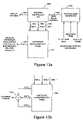
- FIG. 1show a typical UWB transceiver
- FIG. 2shows a block diagram of an infrared data communications transceiver according to an embodiment of an aspect of the present invention
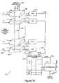
- FIGS. 3 a to 3 eshow, respectively, an example of a combined optical/UWB home wireless mesh network, a schematic diagram of an optical network with a mesh topology, a first example of a processing node on a optical mesh network, a second example of a processing node on a optical mesh network, and an architecture for a node of an optical/UWB network;
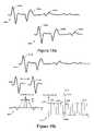
- FIGS. 4 a to 4 dshow, respectively, a transmitted UWB signal comprising a single pulse, an example of a received version of the transmitted pulse of FIG. 4 a with multipath reflections and other propagation effects, a series of transmitted UWB pulses of the type shown in FIG. 4 a , and a received signal corresponding to the transmitted signal of FIG. 4 c showing overlapping multipath reflections;
- FIG. 5shows an overview block diagram of a UWB receiver
- FIG. 6shows a simplified block diagram of a demodulator architecture for use with the receiver of FIG. 5 ;
- FIG. 7shows a timing diagram illustrating timing variations of multipath components of a pulse with respect to pulse repetition frequency
- FIG. 8shows diagrammatically a modulation scheme for use with the demodulator of FIG. 6 ;
- FIGS. 9 a and 9 bshow, respectively, a data frame format and pilot tone pulses for the receiver of FIG. 5 ;
- FIGS. 10 a and 10 bshow, respectively, a optical transmitter and a pulse generator for the transmitter
- FIGS. 11 a and 11 bshow, respectively, a signal acquisition and tracking system for the receiver of FIG. 5 , and a waveform memory data format;
- FIGS. 12 a and 12 bshow, respectively, a flow diagram of a signal acquisition procedure, and a diagrammatic illustration of a signal hunt process
- FIGS. 13 a and 13 bshow, respectively, a reference waveform generation system, and a variant of the system of FIG. 13 a;
- FIG. 14shows a block diagram of a correlator for the demodulator of FIG. 6 ;
- FIGS. 15 a and 15 bshow, respectively, received signals with interleaved multipath components, and a diagrammatic illustration of the operation of the correlator of FIG. 14 .
- FIG. 1shows an example of an analogue UWB transceiver 100 .
- Thiscomprises an transmit/receive antenna 102 with a characteristic impulse response indicated by bandpass filter (BPF) 104 (although in some instances a bandpass filter may be explicitly included), couples to a transmit/receive switch 106 .
- BPFbandpass filter
- the transmit chaincomprises an impulse generator 108 modulatable by a baseband transmit data input 110 , and an antenna driver 112 .
- the drivermay be omitted since only a small output voltage swing is generally required.
- One of a number of modulation techniquesmay be employed, typically either OOK (on-off keying i.e. transmitting or not transmitting a pulse), M-ary amplitude shift keying (pulse amplitude modulation), or PPM (pulse position modulation i.e. dithering the pulse position).
- OOKon-off keying i.e. transmitting or not transmitting a pulse
- M-ary amplitude shift keyingpulse amplitude modulation
- PPMpulse position modulation i.e. dithering the pulse position
- the transmitted pulsehas a duration of ⁇ 1 ns and may have a bandwidth of the order of gigahertz.
- the receive chaintypically comprises a low noise amplifier (LNA) and automatic gain control (AGC) stage 114 followed by a correlator or matched filter (MF) 116 , matched to the received pulse shape so that it outputs an impulse when presented with rf energy having the correct (matching) pulse shape.
- LNAlow noise amplifier
- ADCautomatic gain control
- MFmatched filter
- the output of MF 116is generally digitised by an analogue-to-digital converter (ADC) 118 and then presented to a (digital or software-based) variable gain threshold circuit 120 , the output of which comprises the received data.
- ADCanalogue-to-digital converter
- variable gain threshold circuit 120the output of which comprises the received data.
- FECforward error correction
- block error coding and other channel coding/decoding and baseband processingmay also be employed, but such techniques are well-known and conventional and hence these is omitted for clarity.
- thisshows an embodiment of an optical transceiver 200 , based on a UWB receiver system 210 , in particular the system described later but optionally some other UWB system, such as that shown in FIG. 1 .
- UWB receiver/transmitter 210the receive antenna is replaced by a fast photodiode 202 such as a PIN photodiode, together with a suitable front end LNA (low noise amplifier, for example a transimpedance amplifier) and filter 204 to couple the photodiode to the receiver/transmitter block 210 .
- the transmit antennais replaced by an optical emitter such as a light emitting or laser diode 206 , again coupled to the receiver/transmitter block 210 by a suitable driver 208 .
- an optical output power in the range 1-10 mWmay be employed at a near-IR wavelength such as 785 nm, 808 nm, 875 nm or 976 nm; fast laser diodes sub-nm rise/fall times are readily available.
- the photodiodeis selected so as to be responsive at the transmitter wavelength.
- the system we describecan provide sensitive detection and thus no additional optics are necessary.
- a receiver without additional opticswill generally exhibit a wide acceptance angle, which is often advantageous.
- simple light collection/directional opticssuch as a lens and diffuser may be employed.
- An optical filtersuch as a low (IR)-pass, bandpass or interference filter may be employed for increased sensitivity.
- the receiver/transmitter block 210comprises a single chip UWB receiver/transmitter of the type described in more detail below.
- a common UWB chipmay be interfaced or interfaceable to both optical and UWB radio communications, for example by selectable links or by a switch, optionally under automatic control.
- the optical receiver and/or transmittermay be configured for coupling to a fibre optic, for example as part of a passive optical network.
- a fibre opticfor example as part of a passive optical network.
- Such coupling arrangementsare well known to those skilled in the art, and substantially any conventional coupling arrangement may be employed.
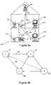
- FIG. 3 ashows an example of a wireless home network 300 comprising a plurality of consumer electronic devices each of which is provided with an optical and/or UWB transceiver and an associated controller to enable it to act as a node on the network.
- nodes on the networkinclude a laptop computer 302 and printer 304 , first and second televisions 306 , 308 , a set top box 310 and a video/DVD player 312 , a video camera 314 , a satellite receiver 316 , and an audio system 318 .
- these devicesare in optical/radio communication with one another although in general not every device will be in communication with every other device.
- the satellite receiver 316may be located in the loft of a building and may therefore only be able to communicate by radio UWB with UWB-enabled devices in upstairs rooms whereas the laptop 302 and printer 304 may communicate using an optical UWB connection.
- FIG. 3 bshows a simplified schematic diagram of an optical/UWB home wireless network such as that shown in FIG. 3 a .
- the networkhas four nodes 330 , 332 , 334 , 336 defining a mesh topology.
- Each nodeis in communication with each other node as illustrated by the solid lines connecting the nodes, except for nodes 330 and 336 which are out of range of one another, as indicated by the dashed line connecting these nodes.
- rangemay be taken to mean range providing an acceptable data rate and/or error rate.
- nodes 330 and 336wish to communicate with one another the communication must be routed via either node 332 or node 334 .
- the topology of the networkis variable since network enabled devices may be physically moved between locations and/or switched on and off. Moreover at times devices may be added to or removed from the network. It is preferable that such network modifications do not require reconfiguration of the network by a user, and in particular that there is no need for configuration of one or more routers as would be the case in a traditional IP (internet protocol) network. It can further be seen that in the networks of FIGS. 3 a and 3 b there is no single network backbone across which traffic could be managed.
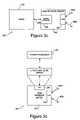
- FIGS. 3 c and 3 dshow two examples of nodes on the network of FIG. 3 b .
- FIG. 3 cshows a node 350 comprising a network device 352 coupled to a video recorder/player 354 by means of a digital link 356 comprising, for example, a coaxial cable or PCI (peripheral component interconnect) connection.
- the network device 352comprises a digital interface 358 for digital link 356 and a UWB transceiver 360 to provide one or more communication channels 362 such as an optical channel 362 a and/or a radio UWB channel 362 b .
- FIG. 3 dshows another example of a node 370 in which like elements to those of FIG. 3 c are indicated by like reference numerals.
- UWB network device 352includes a PCI interface 364 to another processor 366 such as a processor of a DVD player or an Ethernet router.
- network device 352implements a two port MAC (media access control) level bridge to the other processor 366 in a conventional manner.
- link 340 between nodes 330 and 332may utilise a first optical/UWB channel and link 342 between nodes 330 and 334 may utilise a second optical/UWB channel.
- link 342 between nodes 330 and 334may utilise a second optical/UWB channel.
- thismay be implemented using code division multiplexing, different ultra-wide frequency bands or in some other way.
- Theremay be different kinds of channel operating, optical and/or radio UWB channels and, for each, one or more code channels which may be used to distinguish between different concurrent networks or piconets using CDMA techniques.
- the logical communication flow channels within the networkmay be built over these and thus there may be several concurrent logical channels on any given single CDMA domain, either due to a distinction on grounds of QoS (bandwidth or latency control) or simply because there are multiple devices sharing the same CMDA domain by means of time multiplexing.
- Data packets transmitted over the networkpreferably contain some form of logical routing information, which may be either derived from paired MAC addresses in an 802.3 style Ethernet frame or by means of a proprietary header word.
- Communication between two devicesmay use concurrent transmission using different coding, and optionally wavelength bands and/or a combination of radio and optical communications.
- time multiplexingmay be employed, to either multiplex the physical layer (PHY) between different codes and/or wavelengths and/or optical/radio, or to time multiplex different devices sharing a common physical channel.
- PHYphysical layer
- a single transmitter, receiver or transceivermay be time multiplexed or a “separate” transmitter/receiver/transceiver may be provided for each channel.
- a logical transceivermay be provided for each parallel channel up to a maximum number of channels, each of these logical transceivers being accessed by a different logical port.
- FIG. 3 eshows an architecture 380 of a network device for the above described network.
- the devicecomprises a processor 382 which has an address and data bus 384 connecting the processor to programme memory 386 a and data memory 386 b .
- the processoralso has a control bus 388 for reading and writing control data from and to peripheral devices which here comprise one or both of a UWB radio interface 390 and an optical (UWB-based) interface 400 , a second interface 392 to a host processor or device, and a DMA (direct memory access) controller 394 .
- the UWB radio interface 390 and optical interface 400provide multi channel bi-directional communications as schematically indicated by links 390 a, b and 400 a, b ; preferably these incorporate forward error correction.
- the second interface 392may comprise a PCI interface or an Ethernet interface or another optical/UWB interface, and enables the network device to be coupled to a host processor such as a TV, video, computer, set top box and the like.
- a host processorsuch as a TV, video, computer, set top box and the like.
- the network deviceincludes a second data bus 396 which is used for transporting data sent over the network.
- data bus 396is coupled to radio/optical interfaces 390 / 400 and to second interface 392 as well as to buffer memory 398 for buffering transmitted packet data.
- data bus 396is not directly connected to the data bus of processor 382 and instead is controlled by DMA controller 394 , which in preferred embodiments is the only bus master on this data bus to avoid the need for bus arbitration.
- DMA controller 394controls the transfer of data between radio/optical interfaces 390 / 400 , packet buffer memory 398 and second interface 392 .
- Such data transferis indirectly controlled by processor 392 via control bus 388 ; preferably processor 382 is the only bus master on this control bus, again so that no bus arbitration is required.
- data bus 396is further coupled to the data memory 386 b of processor 382 in order to allow data to be exchanged between packet buffer memory 398 and data memory 386 b under control of DMA controller 394 . This allows, for example, packet header data to be transferred to data memory 386 for processing by processor 382 .
- DMA controller 394also has a plurality of registers accessible to the processor using control bus 388 , these registers storing packet control information such as channel handle information as described further below.
- packet control informationsuch as channel handle information as described further below.
- additional memorysuch as Flash memory or SDRAM may be appended to the packet buffer memory 398 , and likewise accessed by DMA controller 394 .
- a transmission medium coupling a UWB transmitter and UWB receiverwhich may comprise a wireless or wired communications channel, will typically give rise to dispersion (which distorts the received pulse shape) and other physical effects that complicate the function of the receiver. These other effects include multiple path reflections, which result in multiple pulses at the receiver for each transmitted pulse, in some cases rf pulses being phase inverted.
- interference and noise sourcesare received in addition to the desired pulse data. Noise sources include thermal noise (from the receiver itself), narrow band interference from transmitters sharing the same frequency spectrum, and broadband interference, from internal logic switching and external sources. There may be further interference from co-located systems. The inventors have recognised that some of these problems, in particular multipath and interference, are common to both UWB and pulsed IR communications links.
- FIG. 4 ashows a transmitted UWB pulse, which in this example has a duration of approximately 100 ps.
- FIG. 4 bshows the same pulse as it might be seen by a UWB receiver.
- the received pulsehas a plurality of multipath components and also exhibits distortion and other propagation effects.
- Multipath componentsare received over a time scale which depends upon the transmission channel but which may, for example, be between 10 ns and 100 ns (the pulses shown in this diagram are not to scale), multipath at the longer end of this range being observed in wired systems such as UWB over mains (AC power cable) transmissions as described in the co-depending UK Patent Application No. 0222828.6 filed on 2nd Oct. 2002.
- the first received multipath componentneed not be the largest (as shown in FIG. 4 b ) and may be significantly distorted or even inverted.
- FIG. 4 cillustrates a series of transmitted pulses
- FIG. 4 dan example of a corresponding received signal. It can be seen that multipath reflections from one pulse may overlap with the first signals from the next pulse. This problem is exacerbated when timing modulation is applied to a transmitted pulse.
- FIG. 5shows a block diagram of a UWB receiver 500 suitable for receiving such signals. We later describe how such a receiver may be adapted for optical use.
- An incoming UWB signalis received by an antenna 502 , which may comprise a capacitive an/or inductive coupling to a cable system such as a mains power cable or a telephone cable.
- the received UWB signalis provided to an analog front end block 504 which comprises a low noise amplifier (LNA) and filter 506 and an analog-to-digital converter 508 .
- a set of counters or registers 510is also provided to capture and record statistics relating to the received UWB input signal.
- the analog front end 504is primarily responsible for converting the received UWB signal into digital form.
- the digitised UWB signal output from front end 504is provided to a demodulation block 512 comprising a correlator bank 514 and a detector 516 .
- the digitised input signalis correlated with a reference signal from a reference signal memory 518 which discriminates against noise and the output of the correlator is then fed to the defector which determines the n (where n is a positive integer) most probable locations and phase values for a received pulse.
- the output of the demodulation block 512is provided to a conventional forward error correction (FEC) block 520 .
- FECforward error correction
- the receiver FEC block 520comprises a trellis or Viterbi state decoder 522 followed by a (de) interlever 524 , a Reed Solomon decoder 526 and (de) scrambler 528 .
- other codings/decoding schemessuch as turbo coding may be employed.
- the output of FEC blockis then passed to a data synchronisation unit 530 comprising a cyclic redundancy check (CRC) block 532 and de-framer 534 .
- the data synchronisation unit 530locks onto and tracks framing within the received data separating MAC (Media Access Control) control information from the application data stream(s) providing a data output to a subsequent MAC block (not shown).
- MACMedia Access Control
- a control processor 536comprising a CPU (Central Processing Unit) with program code and data storage memory is used to control the receiver.
- the primary task of the control processor 536is to maintain the reference signal that is fed to the correlator to track changes in the received signal due to environmental changes (such as the initial determination of the reference wave form, control over gain in the LNA block 506 , and on-going adjustments in the reference wave form to compensate for external changes in the environment).
- the LNA block 506amplifies the signal received from the antenna or cable coupling.
- the amplifier designcontains a fixed frequency passive filter that rejects signals out side of the FCC/ETSC permitted spectral band (3.1-10.6 GHz), as well as rejecting signals from the 5 GHz UNII frequency band. Rejection of such signal areas prevents strong narrow band transmissions from saturating the subsequent A/D converter. It is particularly important to reject signals that are likely to be co-located with a UWB device, such as 802.11, Bluetooth and mobile phone frequencies.
- the LNAalso contains a switchable attenuator that may be used to adjust the signal level fed to the A/D unit.
- the attenuatormay be controlled directly by both the control processor 536 and the reference signal.
- the purpose of the attenuatoris to avoid input saturation at the A/D unit, while maintaining sufficient sensitivity to detect the received pulse waveform.
- the reference waveform from the Detector unitmay also control the attenuation in real time, allowing different gain settings to be applied to different portions of the multipath signals that are received from a single pulse.
- the A/D converter 508may take a variety of forms. In a preferred embodiment the A/D converter 508 is logically configured as a continuous sampler, effectively providing a continuous stream of samples at a suitable rate as determined by the upper frequency of the relevant UWB band and the Nyqust criterion, for example 20 G samples per seconds (20 GHz) for a 10 GHz upper frequency.
- the A/D modulemay comprise a bank of samplers, for example 16 to provide 16 samples for each received pulse, successively triggered by a phase tapped clock to provide a snapshot of a portion of a received UWB signal at different phases which may then be used to provide an input to the correlator banks 514 of demodulation block 512 .
- parallel blocks of signal samplesmay be provided at a rate of a few hundred megahertz, for example at substantially the pulse repetition frequency (PRF) rate thus effectively reducing the primary digitisation clock speed to this rate; preferably each block substantially spans the duration of a received UWB pulse.
- PRFpulse repetition frequency
- fast A/D convertersare the described in the following documents, which are hereby incorporated by referenced: “A 20 GSamples/s 8-Bit A/D Convertor with a 1 MB memory in 0.18 ⁇ CMOS presented by Brian Setterberg of Agilent Technologies, Inc., at the 2003 IEEE International Solid-State Circuit Conference (ISSCC)”; “A Serial-Link Transceiver Based on 8-Gsamples/s A/D and D/A Converters in 0.25 ⁇ m CMOS presented by Chih-Kong Ken Yang, Vladimir Stojanovic, Siamak Modjtahedi, Mark A, Horowitz and William F. Ellersick, IEEE Journal of Solid-State Circuits, Vol 36, No 11, November 2001”; published US Patent Applications 2002 0167373 and 2002 0145484.
- the A/D convertermay either be a single-bit converter or a multi-bit converter, and may either monitor the received voltage level or the power level in the received signal.
- the A/D converter 508may comprise a non-continuous sampler where the sampler is run only around the expected time of arrival of a received pulse (or around a desired time slice when hunting for a received pulse) and is substantially inactive at other times. In this way a high sampling rate may effectively be achieved but with advantages such as reduced power consumption.
- Non-continuous samplingcan offset some of the disadvantages of such a sampler, but can constrain the range of possible delay modulation values that can be detected, thereby reducing the potential information that can be carried by each pulse.
- Such a trade-offis often acceptable in systems where there are many co-located independent pulse transmissions, since the risk of ‘collisions’ between pulses from different transmissions is reduced.
- the AFE 504therefore preferably contains counters that monitor statistics of the input signal conversion, recording the number of values recorded in each of the sampling levels over some period of time.
- Software running on the Control Processorperiodically reads these values and resets the counters. The software may then use these to determine an optimum setting for the gain/attenuation control applied to the received signal by LNA unit 506 . For such purposes, the software may assume that the received signal is, on average, a gaussian noise signal.
- LNA/filter 506may be replaced by optical transceiver components, but substantially the same A/D converter and subsequent signal processing circuitry may be employed as for rf UWB.
- A/Doperates in a zero-crossing mode, with a 1-bit converter allocating a binary one to positive signal values and a binary zero to negative signal values or vice-versa
- the A/Dis run at an offset from zero, defining a “slicing level” to provide a peak detect function.
- the sample “slicing” thresholdis adjustable, and in embodiments this may be automatically adjusted in response to the received signal level and/or to recorded statistics relating to the received signal level and/or to a level of the stored reference signal for the received signal.
- a 1-bit A/Dis used, the 1-bit sample performing an energy detect function, although in other embodiments a multibit A/D may be employed.
- thisis responsible for extracting a data signal imposed on the pulses by a transmitter.
- the scheme described hereis specifically designed to decode modulation by means of the pulse arrival time or by the pulse phase. It may also be adapted to detect modulation by means of the pulse shape (spectral modulation).
- the input to the demodulatoris a stream of sample data from the AFE 504 ; the output is a stream of decoded data bits.
- the output data rateis substantially constant fixed by the PRF (Pulse Repetition Frequency) and the number of bits encoded by each pulse.
- PRFPulse Repetition Frequency
- the operating parameters of the demodulatorPRF and bit-encoding
- PRF and bit-encodingare typically fixed for a given transmitter.
- the demodulatorand other system parameters, such as AFE gain
- the demodulatorcontains units to correlate the received signal against a reference signal (programmed and maintained to track changes in the external signal propagation environment) by control processor 536 .
- the detailed form of the demodulatoris shown in FIG. 6 .
- thisshows a simplified block diagram of demodulator 512 of FIG. 5 ; like elements to those of FIG. 5 are indicated by like reference numerals.
- the input from the wireless antenna or wired interface and amplifier/filter unit 506is implemented in discrete analog circuitry, and the A/D (sampler) 508 and demodulator 512 are implemented in the sampling clock domain which has, in one embodiment, an effective range of 25 GHz, corresponding to an actual clock rate of 250 MHz.
- the system control logic and output to the forward error correction apparatusalso operates at 250 MHz.
- the correlator 514comprises a bank of multiply-accumulate units 600 each of which receives an input signal sample (comprising a set of samples of the input signal at successive sampling intervals) and multiplies this by a reference sample (comprising a set of samples of a reference waveform at successive sampling intervals) provided by reference waveform synthesiser 518 .
- the multiplier operationmay be implemented using a simple XOR gate.
- the accumulatorsaverage the (correlation) data over a number of pulses, by averaging over (successive) transmitted pulses bearing the same encoded data and/or averaging over multipath components.
- the reference signal generator or synthesiser 518provides the reference signal to the multiply-accumulate units 600 under control of a pattern sequencer 602 .
- the pattern sequenceris controlled by a PSR (Pseudo Random) sequence lock acquisition module 604 , preferably implemented in software as described later.
- the pattern sequencer 602provides a reference waveform 606 to a plurality of delay units 608 to provide a plurality of successively delayed versions of the reference waveform to multiply-accumulate units 600 .
- the reference waveformis preferably applied in parallel to the multiply-accumulate units 600 as described later.
- the reference signal for the correlatoris programmed into the reference signal generator 518 by software running on control processor 536 , which preferably uses a training algorithm to determine the receiver response (that is, amplitude and phase distortion to a transmitted pulse).
- the control processor 536also maintains a clock phase locked to the PRF (Pulse Repetition Frequency) of the transmitter from which signals are being received by using the arrival times of detected pulses relative to an internal timing reference (Local Crystal Oscillator).
- a power control output 610 from the reference waveform generatormay also be employed to gate power to the A/D and sampling circuitry 508 to put this circuitry into a reduced power mode in periods where there is no expected received signal. This is particularly advantageous in systems using a multi-bit A/D since these often have a relatively large power consumption.
- a multiply-accumulate unit 600provide outputs to a discriminator 612 which determines the sign and peak value (or values if probabilistic outputs are supplied to the following stage of the (absolute) value maximum accumulator output).
- the discriminator outputsprovide an output data signal identifying the position of a received pulse and the pulse phase (that is, normal or inverted).
- a constellation decodermaps this position/phase data from the discriminator to an n-bit symbol which is then passed to the forward error correction block 520 .
- the demodulator 512has a plurality of interfaces to other parts of the receiver system, each of which is preferably via a data synchroniser 616 a, b, c , such as a register or buffer.
- the multiply-accumulate units 600provide an output to the control processor 536 for calibration of the receiver front end (and preferably also the transmission channel) and for location processing to facilitate physical location of a UWB receiver according to known techniques.
- the interface between the constellation decoder 614 and FEC blocks 520is preferably also implemented via a buffer.
- the PSR lock acquisition module 502preferably has a bi-directional interface to a software control function implemented on control processor 536 to provide functions such as physical location of the receiver, delay tracking, and data (de) whitening.
- thisshows relative timings of transmitted data pulses and multipath components of such pulses as seen by the receiver.
- a typical delay span for a multipath reflectionis between 1 and 100 ns whereas a typical interval between successive transmitted data pulses is between 2 and 10 ns. It can therefore be appreciated that a multipath reflection of a one pulse may arrive following a direct, line of sight transmission of the next pulse, or even of the next few pulses.
- the multipath reflectionsmay also be phase inverted subject to different path distortions from the direct path.
- the multiply-accumulate stages 600 of the correlatoronly integrate multipath energy over the inter-transmit pulse period so that, for example in FIG. 7 , multipath components arriving outside the 2-10 ns delay range would be ignored.
- typical multipath delaysare greater than the average inter-transmit pulse period, and thus significant energy may be lost with this approach. The problem is exacerbated if pseudo-random timing jitter is applied to the timing of the transmitted pulses to achieve spectral whitening.
- correlator banksthat is banks of multiply-accumulate units 600 as shown in FIG. 6 , parallel to facilitate pipelining of the pulse integrations.
- Such parallelismimplemented by repetition of the correlator logic but in a preferred arrangement this parallelism is achieved by multiplexing the use of a single set of multiply-accumulate chains 600 , for example by keeping track of distinct sets of accumulator values in a static RAM (Random Access Memory) buffer memory.
- FIG. 8shows a schematic diagram of a UWB signal employing a preferred modulation scheme for the above described receiver and which may be generated by a transmitter described later with reference to FIG. 10 .
- the signal of FIG. 8may be employed in a wireless or wired UWB transmission system.
- a similar signalmay be employed in a wireless or wired optical data communications system, although with positive-going pulses from zero rather than a mid-point baseline.
- the signal 800comprises a plurality of wavelets or pulses 802 each of which has either a normal or inverted form to encode a single bit of information data to be transmitted;
- FIG. 8shows two normal (rather than inverted) examples of such pulses.
- a wavelet or pulsecomprises a positive-going portion 802 a and negative-going portion 802 b ; the order of these two portions may be reversed to invert the pulse, thus facilitating generation of normal and inverted pulses in hardware (in an optical system such phase modulation may be omitted).
- the pulses 802have a nominal pulse repetition frequency, for example of the order of 100 MHz.
- an additional one or more information data bitsmay be modulated onto signal 800 by varying the precise position (timing) of a pulse dependent upon the data to be transmitted.
- timingFor various reasons bi-phase modulation of a rf UWB signal has been the preferred modulation of many applications.
- the optical systems we are primarily concerned with herevary the pulse position to encode data onto the optical-UWB signal.
- the pulse positionmay also be dependent upon a pseudo random or PN (pseudo noise) signal.
- Such a pseudo random sequenceis preferably deterministic so that although apparently random once the sequence and start point is known it can be reconstructed in a deterministic manner at the receiver to allow this PN modulation to be effectively subtracted from the received signal or compensated for in other ways.
- the PN modulationis greater than the information data modulation since having a relatively small range of pulse positions about an expected pulse position (once the effects of PN modulation have been compensated for) simplifies demodulation of position-encoded data.
- the positions a pulse can take in response modulation by information dataare separated by one (or more generally an integral number) of reference (and input) signal sampling intervals.
- a pulse 802may take one of eight or 16 different positions in time (although other numbers of positions may be employed) and correlator 514 correlates the input signal with reference signals at all of these positions substantially in parallel to, in a parallel operation, locate the actual or most likely position of a received pulse. As shown in FIG.
- the duration of a single doubletis typically between 50 ps and 100 ps and the correlator bank 514 performs parallel correlation operations over a time window 804 of approximately Ins, thus identifying the pulse as being in one of around 16 overlapping positions.
- the above timings, and the number of parallel multiply-accumulate units 600 of correlator 514may be varied according to the requirements of a particular implementation or application.
- FIG. 9 ashows one example of an MAC frame 900 for use with the receiver 500 when receiving a signal of the type shown in FIG. 8 .
- This MAC frameis, however, provided merely for illustrative purposes and many other different frame formats may be employed.
- the example MAC frame 900begins with a preamble sequence 902 comprising 32 bits of preamble data, for example pseudo random data for training. This is followed by a 4 byte header comprising a pseudo random sequence identifier and a pseudo random sequence seed (for identifying a starting point in a sequence), for example as a pair of 2 byte values.
- Different pseudo random sequencesmay be employed by different transmitters to help avoid collisions between transmitted UWB data signals.
- the headeris preferably structured to give the appearance of noise, and may therefore include a whitening function—for example the pseudo random sequence identifier and seed may each be selected so that the header appears essentially random.
- the headeris followed by payload data 906 which may also be whitened of a fixed or variable length, for example 128 bytes.
- FIG. 9 bschematically illustrates the positions of pilot tone pulses within an optical-UWB signal 910 also comprising information-carrying pulses (not shown).
- one in every 100 pulsescomprises a pilot tone pulse and, as can be seen from FIG. 9 b , these pilot tone pulses occur at regularly spaced intervals to provide a low-level pilot tone.
- the positions (in time) of the pilot tone pulsesmay be modulated to provide timing jitter, allowing more frequent or stronger pilot tone pulses within the spectral mask, although this is not necessary.
- FIGS. 10 a and 10 billustrate an example of a transmitter 1000 which may be employed to generate an information data modulated optical signal 800 as described above with reference to FIG. 8 .
- the transmitter structure of FIG. 10is provided by way of example only and other transmitter structures may also be employed to generate an optical signal for the systems described herein. For simplicity forward error coding arrangements are not explicitly shown in the figure.
- a clock 1002 operating at, for example, 250 MHzprovides a clock signal to a chain of delay elements 1004 a - e each providing a delay of, in this example, 40 ps.
- the successively delayed versions of the clock signalare provided to each of a plurality of monostable pulse generators 1006 , each of which also receives an enable and control input from a controller 1008 .
- a monostable 1006When enabled by the controller 1008 a monostable 1006 provides an output pulse doublet; the phase (normal or inverted) of the pulse doublet is also controllable by controller 1008 .
- the outputs from all of the monostable pulse generators 1006are combined, in this example in summers 1009 and the combined output is provided to an optical emitter 1010 , for example an LED or laser diode (in this block diagram the block 1010 also includes suitable drive circuitry for the emitter).
- the controller 1008receives a pseudo random sequence input from a pseudo noise generator 1012 , and also receives a data and control input 1014 , for example from a preceding forward error correction block and from a transmitter control processor.
- the data and control inputreceives information data to be transmitted by the transmitter and control signals such as a timing control signal to control when the transmitter is to transmit and/or pseudo noise sequence selection and start point control signals.
- the controller 1008may comprise a state machine implemented in either software or dedicated hardware or a combination of the two.
- controller 1008controls the timing of transmitted UWB pulses and the phase (normal or inverted) of these pulses by providing appropriate enable and phase control signals to the monostable pulse generators 1006 which are then triggered to provide output pulses at the corresponding time by the phase tapped clock from clock signal generator 1002 .
- FIG. 10 bthis shows an example of one implementation of a monostable 1006 for the transmitter of FIG. 10 a .
- the monostablecomprises two pulse generators 1020 a, b , one providing a positive-going pulse, the other providing a negative-going pulse, outputs from these two pulse generators being combined in a summer 1022 to provide a pulse doublet output signal 1024 .
- Both of pulse generators 1020 a and 1020 bare controlled by a common enable line 1026 which when asserted enables the pulse generators to provide an output pulse in response to an input timing reference signal on line 1028 , but which when de-asserted disables the pulse generators from providing their outputs.
- an rf system pulse generator 1020 bmay in addition have a delay signal input 1030 which delays the production of its output pulse by two cycles to effectively invert the pulse doublet.
- a pulse doubletcomprising either a positive or negative-going pulse or a negative then positive-going pulse is provided.
- a transmittersuch as a transmitter 1000 of FIG. 10 may be combined with an optical receiver, for example providing an optical input for the front end of the receiver of FIG. 5 , to provide an optical transceiver.
- the transmitter and receiver portions of the transceiverare synchronised to a common PRF clock to avoid self-collision, that is to avoid jamming reception of transmissions from a remote transmitter by local transmissions.
- FIG. 11shows details of a receiver similar to that shown in FIG. 5 , but intended for optical use.
- the signal acquisition and locking systemincluding details of the reference signal capture signal, are shown.
- Like elements of those to FIGS. 5 and 6are shown by like reference numerals.
- the functions of the PSR lock acquisition module 604are provided by a phase control processor and the functions of the pattern sequencer 602 of FIG. 6 are provided by a combination of a reference waveform data table and of a PSR sequence generator.
- the receiverincludes a photodiode 202 to provide an optical input for the receiver, the photodiode interfacing to analog front end and A/D converter 504 .
- This front endprovides a plurality of examples of a received optical input signal in parallel to correlator 514 and each set of input signal samples is processed by a correlator comprising one of multiply-accumulate units 600 of correlator 514 to correlate the set of received samples in parallel with sets of reference signals representing differently delayed pulses.
- the sets of samples defining differently delayed versions of a referenced signal pulseare derived from a waveform of a pulse stored in a reference waveform data table 1100 .
- a reference received pulseis preferably stored in this table as a pulse shaped for each of a set of multi part components of the pulse together with data representing delay intervals between these multipath components, as shown in FIG. 11 b .
- differently delayed versions of a pulsemay be provided by accessing a common wave shape data store for the pulse.
- a reference or template waveform for a single received pulse having a plurality of multipath componentscomprises sample data 102 for a plurality of successive sample points of a multipath component of a pulse followed by delay data 1104 representing an interval between that multipath component of the pulse and the next multipath component.
- An input 1106allows reference waveform data to be written into the referenced waveform data table 1100 .
- Reference waveform datais provided to the correlator 514 from the data table 1100 under control of a PSR sequence generator 1108 in synchronism with a PRF clock input 1110 .
- a phase control processor 1112provides a PRF clock to sequence generator 1108 and reference waveform data to data table 1100 .
- the phase control processorincludes a processor and non-volatile program memory storing program code for pilot tone identification, to provide a software phase locked loop (PLL), for multipath component identification, and for template wave shape retrieval and storage.
- a clock 1114provides a clock signal to the phase control processor and receives tracking data from processor 1112 comprising a time advance/retard signal for controlling the phase of the clock and a frequency increase/decrease for controlling the frequency of the clock when the phase needs to be consistently advanced/retarded.
- the clock 1114is thus adjustable to track movement of the receiver with respect to the transmitter by means of systematic adjustment in the clock timing (which are generally small compared with the modulation).
- clock 1114acts as a slave to a similar clock in a remote transmitter and thus acts as a link clock; typically it has a frequency in the range 50-250 MHz.
- the phase control processor 1112provides a control output to a transmitter 1116 , such as transmitter 1000 in FIG. 10 , to control the transmitter to provide an optical signal from an optical emitter 1118 for use in training receiver.
- the control processor 1112also receives a start of frame input signal 1120 from a MAC state machine implemented in either hardware or software.
- the phase control processor 1112further receives a set of inputs 1122 , one from each accumulator of correlator 514 , and a further input 1124 from the output of discriminator 612 .
- the phase control processor 1112programs the reference waveform data table 1100 with an initial, predetermined wave shape and then identifies the signal pilot tone and runs a software phase lock loop to lock onto this tone to provide a time reference. The processor then uses this to identify the wave shape of a received pulse, including its multipath components.
- the processor 1112may apply a Fast Fourier Transform (FFT) filter to remove narrow band interference.
- FFTFast Fourier Transform
- the multipath component with the strongest signalis identified and the shape of this multipath component of the pulse determined from the input data, and then the processor hunts for other multipath components both backwards and forwards from the strongest signal (because the direct line of sight pulse may not be the strongest).
- the correlatoroperates with blocks of eight or 16 samples and these blocks are effectively positional in time with respect to the link clock reference from clock generator 1114 .
- the multipath component pulse tracking procedureis repeated at a frequency in the order of kilohertz in order to track variations in the multipath channel and, in embodiments where implemented, to obtain physical location information relating to the receiver's position.
- the multipath environmentmay be quasi-static in which case a channel characterisation procedure such as that described above may only be applied at switch on or, for example, when the error rate increases above a threshold.
- phase control processorreceives sampled input signal data via the correlator 514 .
- processor 1112may receive sampled input signal data directly from analog front end 504 .
- the input datamay be correlated with a delta function such as a spike or impulse written into the wave form data table.
- FIG. 12 ashows a flow diagram explaining further the operation of the phase control processor 1112 of FIG. 11 a .
- the control processorinstructs transmitter 1116 to transmit local optical pulses under control of the local clock generator 1114 .
- These pulsesare received at a very high signal level and, moreover, processor 1112 knows when these pulses are transmitted and thus knows at what position in time the received input data is expected to comprise a transmitted pulse (taking account of the delay introduced by the separation between transmit antenna 1118 and receive antenna 502 (typically one or a few centimeters)).
- processor 1112programs wave form data table 1100 with a predetermined template, in particular an impulse, and hunts for the transmitted pulses by controlling the timing of PSR sequence generator 1108 . This is conveniently performed by inhibiting generation of a pseudo random sequence so that the phase of the output of generator 1108 may be varied by using the PSR seed as a phase offset adjust.
- the wave shape of a pulse as received and digitised by analog front end 504is read from correlator 514 and written into the referenced wave form data table to serve as an initial reference wave form. This in effect calibrates out phase and gain non-linearities in the receiver front end.
- the locally received signalis strong the wave shape data written into the data table 1100 may optionally comprise an average of a plurality of received pulses.
- processor 1112controls the receiver to hunt for a signal at the pulse repetition frequency of the remote transmitter, that is at the pilot tone of the remote transmitter.
- the pilot tone frequencymay not be known exactly but in preferred arrangements is limited to a small set of possible frequencies such as 50 MHz, 100 MHz, and 250 MHz and thus the receiver can pick each of these frequencies in turn to look for incoming signals.
- the process of hunting for a signal at PRFis illustrated in FIG. 12 b .
- the receiver systemfirst runs a correlation in a set of windows 1210 spaced by intervals at the PRF frequency, averaging the correlation results over a plurality of such windows and, if no significant correlation is found, slips the windows, at the same frequency, to a slightly delayed position 1212 as shown in timeline (ii) to repeat the correlation and averaging procedure until pulses at the PRF are found.
- the correlator 514provides a plurality of outputs corresponding to a small range of delays either side of a desired time position it is straightforward to track variations in the PRF.
- the clock generator 1114(and the equivalent in the transmitter) is preferably crystal controlled and thus relatively stable and varies only slowly compared with the kilohertz PLL tracking frequency.
- the more difficult taskis to locate the remote transmitter PRF in the first place, particularly as a pilot tone pulse is transmitted for of the order of only one in 100 pulses, and because the signal is relatively low level, especially at longer ranges.
- These difficultiesare addressed by averaging over a relatively long period in order to identify the systematic pilot tone impulses which appear at fixed times and distinguish, for example, from other pulses which appear effectively at random times.
- the processorcan rely on the relative stability of clock generator 1114 and can thus rewrite the referenced wave form data table 1100 with an impulse and average over a plurality of pulses, typically between 100 and 1000 pulses, to determine the reference wave form for the transmit channel, and can then write this into the wave form data table.
- the number of pulses over which the signal needs to be averageddepends upon the range—one pulse may be enough at one meter and average of 104 pulses may be necessary at a range of 30 meters.
- phase control processor 1112can hunt backwards and forwards from this to identify the next multipath component of the pilot tone, and this can be repeated to determine data for a plurality of multipath components of a transmitted pulse.
- the number of multipath components for which data is acquireddepends upon a trade off between acquisition time and system sensitivity (capturing energy from more multipath components facilitates greater sensitivity but takes longer to acquire). It will be appreciated that once the pulse shapes and delays for multipath components of a pulse have been located in time and samples stored tracking the variations of these over time is relatively straightforward and may be accomplished by periodically averaging over say 100 to 1000 pulses, for example by time multiplexing correlator in a similar way to that described below.
- FIGS. 13 a and 13 bshow details of the reference wave form generation system.
- the PSR sequence generator 1108receives control signals from the control processor 1112 comprising a pilot tone to control the timing of the reference wave form generation, and a starter frame signal and a sequence seed to control the pseudo random sequence modulation for pulse position dithering, and provides a read timing control output 1302 to a pattern controller 1300 .
- FIG. 15 athis shows the received multipath components of two successively transmitted pulses 1500 and 1502 , each with a plurality of multipath components 1500 a - c , 1502 a - c .
- the multipath components 1500 a, b of pulse 1500arrive before the start of pulse 1502 but that the multipath component 1500 c of pulse 1500 arrives between multipath components 1502 a and 1502 b of pulse 1502 .
- the reference wave form data table 1100should preferably be able to provide the appropriate multipath component of the pulses at the appropriate times even when these are interleaved as shown. Although this is not essential it is preferable in order to be able to retrieve energy from more multipath components of a received signal.
- a pattern generator 1300provides a plurality of outputs 1304 for providing reference wave forms corresponding to a plurality of transmitted pulses having overlapping multipath components.
- pattern controller 1300provides two address outputs 1304 for addressing the wave form data table at appropriate times to provide portions of the reference wave form corresponding to the overlapping or interleaved portions of the multipath components.
- a pattern controller 1300provides a first address output for controlling data table 1100 to provide multipath components 1500 a, b, c and a second address output for addressing the table to provide the reference wave shapes for multipath components 1502 a, b, c at appropriate times. It will be appreciated that the number of address outputs of pattern controller 1300 depends upon the delay span of the number of significant multipath components of a pulse as compared with the inter-transmit pulse spacing.
- the reference wave form data table 1100provides an output 1306 which comprises a time ordered combination of the multipath components of successfully transmitted components in the example of FIG. 15 a multipath components 1500 a , 1500 b , 1502 a , 1502 c , 1502 b and so forth.
- a single set of outputsprovides these multipath components in a time multiplexed fashion for use with correlator 514 also operating in a time sliced or multiplexed configuration.
- data table 1100has a plurality of sets of outputs, one for each transmitted pulse the receiver is concurrently able to process, which are combined in a summer 1310 and provided as a combined output for subsequent correlation.
- the data table memoryis configured to provide a plurality of blocks of reference signal data in parallel, each block of data being delayed with respect to a previous block of data.
- a block of datamay comprise, for example, eight or 16 sample values of the stored reference wave form, preferably defining a multipath component of a pulse such as a one of components 1500 a, b, c of FIG. 15 a .
- the blockspreferably overlap in time and in one arrangement each block is delayed from the previous block by one sample, 16 blocks defining 16 successively delayed multipath pulse components being output in parallel.
- thisrequires a bus comprising 256 parallel outputs from reference output data table 100 , but the majority of these outputs may be provided simply by appropriate wiring since 16 blocks each of 16 samples, each delayed by a sample requires only 32 parallel sample value outputs.
- Each of these sample value outputsmay comprise a single or multi-bit value, depending upon whether or single or multi-bit A/D conversion is employed.
- a block of reference datamay be added with zeros at either or both ends.
- reference wave form data tableprovides important benefits to the receiver system, in particular allowing use of a lower quality receiver analog front end than would otherwise be acceptable as the above described process of self-calibration, storing referenced wave form data table 1100 , can compensate for distortion within the receiver as previously described.
- the PSR sequence generator 1108is responsive to the pseudo random sequence employed for transmitting the data to control the read timing from the reference wave form data table to compensate for the pseudo random (but deterministic) time modulation imposed on the variable, information—dependent phase and position modulation.
- Pattern controller 1300also provides an end of pattern output signal 1308 for use in resetting the correlator as described further below.
- FIG. 14shows details of the configuration of the multiply-accumulate units of correlator 514 .
- the correlatorcomprises a plurality, in one configuration 16 , of multiply units 1400 each coupled to a respective accumulator 1402 .
- Each multiplier unit 1400receives the same block 1404 of sampled input data, as illustrated comprising 16 successively delayed samples (either one or multi-bit values).
- Each multiply unit 1400also receives a block of reference signal samples 1406 , in one configuration comprising 16 successive samples of the reference signal wave form, from data table 1100 , but each of blocks 1406 is successively delayed so that the sampled input data is correlated in parallel by multiplier units 1400 with portions of the referenced signal wave form spanning a range (as illustrated, 16) of successive time slices of the referenced wave form.
- the effect of thisis to slide the sampled input data block or time slice along the referenced wave form until a correlation is found but it is easier in practice to firstly change the referenced wave form delay rather than the sampled received data delay, and secondly to perform a plurality of correlation in parallel rather than employ a single slide window.
- Each of multiply units 1400comprises a multiplier to multiply each input data sample with the corresponding reference data sample and provide an output to the corresponding accumulator 1402 so that the accumulator accumulates a correlation value from all (in this case 16) correlation operations in parallel.
- Each accumulatorhas an output 1408 coupled to a partial correlation store 1410 for writing an accumulated correlation value into the store.
- Each accumulatoralso has an input 1412 from a read output of store 1410 to allow a partial correlation value written into the store to be read back from the store and added to a further correlation value in each respective accumulator. Writing of data into the store and reading of data from the store is controlled by the phase control processor 1112 .
- the partial correlation store 1410comprises a plurality of sets of memory locations, each set of memory locations storing a set of partial correlation values, one from each multiply-accumulate module (T 1 . . . T 16 ). Storage is provided for as many sets of partial correlation values as is needed to process a desired number of transmitted pulses as overlapping or interleaved multipath components. Thus, for example, two sets of memory locations for partial correlation values are provided for storing partial correlation values where multipath components of two successively transmitted pulses overlap or interleave.
- Discriminator 512Data from each of the plurality of memory locations of a set of partial correlation results is provided on an output 1414 to discriminator module 612 .
- Discriminator 512also provides a memory clear output 1416 for clearing or setting to zero a set of partial correlation values, and receives an end of pattern signal 1308 from pattern controller 1300 .
- Discriminator 612provides an output 1418 to subsequent forward error correction modules such as a Viterbi decoder.
- FIGS. 15 a and 15 bshow waveforms from rf UWB signals but similar principles apply when correlating optical UWB-type signals.
- the procedureis to correlate (accumulate) the first received multipath component 1500 a and to dump this into store 1410 , and then to correlate the next multipath component 1500 b , also accumulating the previously stored partial correlation for multipath component 1500 a by reading this from store 1410 adding this to the partial correlation value of multipath component 1500 b , and the total accumulated set of correlation values is then written back into store 1410 .
- This processis continued until a multipath component of a subsequent pulse is encountered, in this case multipath component 1502 a of pulse 1500 .
- the reference wave form data table 1100controls the reference wave form data table 1100 to provide a pulse shape appropriate for correlating with multipath component 1502 a and following the correlation operation the result of this correlation is dumped into a separate set of memory locations within store 1410 , this set of memory locations being allocated to the second pulse.
- the correlation operation for multipath components of the received signalcontinues with the partial correlation results being written into the set of memory locations for either the first or second pulse as appropriate, the pattern generator controlling the wave form data table to generate a reference wave shape for the appropriate multipath component.
- a multipath component 1500 c of the first pulseis next accumulated with the partial correlation value read from store 1410 for the first pulse and dumped back into store 1410 .
- thisis the final processed multipath component pulse of 1500 though the accumulated correlation values in store 1410 for the first pulse can then be taken as complete correlation values and processed by discriminator 612 .
- the signal indicating that the complete set of multipath components has been correlatedis provided by pattern controller 1300 since this controller is able to determine that the final stored multipath component has been processed.
- correlation of pulse 1502continues with multipath component 1502 b and when the first multipath component of a third pulse (is not shown in FIG. 1500 a ) received the set of partial correlation values which was previously used for pulse 1500 (and which was cleared by discriminator 612 after the complete correlation values for pulse 1500 were processed) is available for use for accumulating correlation values for this third pulse.
- FIG. 15 billustrates, diagrammatically, the correlation of a multipath component 1510 a of a received signal pulse 1510 with a set of referenced pulses 1512 a, b of which, for clarity, only two are shown.
- the referenced signal pulsesare time shifted to either side of the received multipath component 1510 a and correlation with each of these referenced signal pulses provides a correlation value as schematically illustrated in graph 1514 .
- the shape of this curve, and the height and width of its peakmay alter depending upon the received signal and referenced signal shape.
- each bar 1518represents an accumulated correlation value for one of the delayed versions of the referenced signal multipath component 1512 . It can be seen that most of the accumulated correlation values are close to a mean level 1520 but one of the accumulated values represented by bar 1522 is significantly different from the others. This represents the most likely pulse position; the bars 1524 , 1526 to either side of it represents next most probable pulse positions.
- Bar 1522 ais significantly greater than the average 1520 which applies a positive correlation (normal pulse) whilst bar 1522 b has a correlation value which is significantly less (more negative) than the average which implies a negative correlation that is an inverted received signal pulse as compared with the reference.
- the correlator of FIG. 14 bis able to co-determine both the likely position (in time) of a received signal pulse and also the phase (normal or inverted) of the pulse and hence to co-determine information data modulated to both pulse position and pulse phase simultaneously.
- the use of both position and phase simultaneously to encode information datasignificantly enhances the information data carrying capacity of the system.
- the correlatoris employed for correlating successive multipath components of received signal pulses.
- a transmitter and/or receivermay employ redundancy, using two or more transmit pulses to carry substantially the same data, at the receiver processing these as though they were merely multipath components of a single pulse.
- Such an arrangementmay be employed adaptively, reducing the data rate but increasing reliability where transmission conditions are difficult or at the edge of range of a system.
- the reduction in effective data ratemay be partially compensated for by increasing the pulse repetition frequency; the transmit power may also be adaptively controlled to facilitate this.
Landscapes
- Physics & Mathematics (AREA)
- Engineering & Computer Science (AREA)
- Computer Networks & Wireless Communication (AREA)
- Signal Processing (AREA)
- Electromagnetism (AREA)
- Spectroscopy & Molecular Physics (AREA)
- Optical Communication System (AREA)
- Mobile Radio Communication Systems (AREA)
Abstract
Description
Claims (18)
Priority Applications (1)
| Application Number | Priority Date | Filing Date | Title |
|---|---|---|---|
| US11/222,047US20070025738A1 (en) | 2005-07-28 | 2005-09-09 | Communications systems and methods |
Applications Claiming Priority (2)
| Application Number | Priority Date | Filing Date | Title |
|---|---|---|---|
| GB0515522.1 | 2005-07-28 | ||
| GB0515522AGB2428949B (en) | 2005-07-28 | 2005-07-28 | Communications systems and methods |
Related Child Applications (1)
| Application Number | Title | Priority Date | Filing Date |
|---|---|---|---|
| US11/222,047Continuation-In-PartUS20070025738A1 (en) | 2005-07-28 | 2005-09-09 | Communications systems and methods |
Publications (2)
| Publication Number | Publication Date |
|---|---|
| US20070025739A1 US20070025739A1 (en) | 2007-02-01 |
| US7580643B2true US7580643B2 (en) | 2009-08-25 |
Family
ID=34983650
Family Applications (1)
| Application Number | Title | Priority Date | Filing Date |
|---|---|---|---|
| US11/192,415Expired - Fee RelatedUS7580643B2 (en) | 2005-07-28 | 2005-07-29 | Communications systems and methods |
Country Status (2)
| Country | Link |
|---|---|
| US (1) | US7580643B2 (en) |
| GB (2) | GB2428949B (en) |
Cited By (172)
| Publication number | Priority date | Publication date | Assignee | Title |
|---|---|---|---|---|
| US20090268910A1 (en)* | 2008-04-28 | 2009-10-29 | Samsung Electronics Co., Ltd. | Apparatus and method for initialization of a scrambling sequence for a downlink reference signal in a wireless network |
| US20100272189A1 (en)* | 2006-09-15 | 2010-10-28 | Hyoung Gon Lee | Dtv transmitting system and receiving system and method of processing broadcast data |
| US20110170690A1 (en)* | 2008-02-08 | 2011-07-14 | Celight, Inc. | Secure orthogonal frequency multiplexed optical communications |
| US20120007583A1 (en)* | 2010-07-07 | 2012-01-12 | Ou Eliko Tehnoloogia Arenduskeskus | Method and device for frequency response measurement |
| US20120086345A1 (en)* | 2011-11-20 | 2012-04-12 | Tran Bao Q | Solid state light system with broadband optical communication capability |
| US9119127B1 (en) | 2012-12-05 | 2015-08-25 | At&T Intellectual Property I, Lp | Backhaul link for distributed antenna system |
| US9154966B2 (en) | 2013-11-06 | 2015-10-06 | At&T Intellectual Property I, Lp | Surface-wave communications and methods thereof |
| US9209902B2 (en) | 2013-12-10 | 2015-12-08 | At&T Intellectual Property I, L.P. | Quasi-optical coupler |
| US9312919B1 (en) | 2014-10-21 | 2016-04-12 | At&T Intellectual Property I, Lp | Transmission device with impairment compensation and methods for use therewith |
| US9310064B2 (en) | 2013-03-17 | 2016-04-12 | Bao Tran | Liquid cooled light bulb |
| US9461706B1 (en) | 2015-07-31 | 2016-10-04 | At&T Intellectual Property I, Lp | Method and apparatus for exchanging communication signals |
| US9490869B1 (en) | 2015-05-14 | 2016-11-08 | At&T Intellectual Property I, L.P. | Transmission medium having multiple cores and methods for use therewith |
| US9503189B2 (en) | 2014-10-10 | 2016-11-22 | At&T Intellectual Property I, L.P. | Method and apparatus for arranging communication sessions in a communication system |
| US9509415B1 (en) | 2015-06-25 | 2016-11-29 | At&T Intellectual Property I, L.P. | Methods and apparatus for inducing a fundamental wave mode on a transmission medium |
| US9520945B2 (en) | 2014-10-21 | 2016-12-13 | At&T Intellectual Property I, L.P. | Apparatus for providing communication services and methods thereof |
| US9525524B2 (en) | 2013-05-31 | 2016-12-20 | At&T Intellectual Property I, L.P. | Remote distributed antenna system |
| US9525210B2 (en) | 2014-10-21 | 2016-12-20 | At&T Intellectual Property I, L.P. | Guided-wave transmission device with non-fundamental mode propagation and methods for use therewith |
| US9531427B2 (en) | 2014-11-20 | 2016-12-27 | At&T Intellectual Property I, L.P. | Transmission device with mode division multiplexing and methods for use therewith |
| US9564947B2 (en) | 2014-10-21 | 2017-02-07 | At&T Intellectual Property I, L.P. | Guided-wave transmission device with diversity and methods for use therewith |
| US9577307B2 (en) | 2014-10-21 | 2017-02-21 | At&T Intellectual Property I, L.P. | Guided-wave transmission device and methods for use therewith |
| US9608692B2 (en) | 2015-06-11 | 2017-03-28 | At&T Intellectual Property I, L.P. | Repeater and methods for use therewith |
| US9608740B2 (en) | 2015-07-15 | 2017-03-28 | At&T Intellectual Property I, L.P. | Method and apparatus for launching a wave mode that mitigates interference |
| US9615269B2 (en) | 2014-10-02 | 2017-04-04 | At&T Intellectual Property I, L.P. | Method and apparatus that provides fault tolerance in a communication network |
| US9628854B2 (en) | 2014-09-29 | 2017-04-18 | At&T Intellectual Property I, L.P. | Method and apparatus for distributing content in a communication network |
| US9628116B2 (en) | 2015-07-14 | 2017-04-18 | At&T Intellectual Property I, L.P. | Apparatus and methods for transmitting wireless signals |
| US9640850B2 (en) | 2015-06-25 | 2017-05-02 | At&T Intellectual Property I, L.P. | Methods and apparatus for inducing a non-fundamental wave mode on a transmission medium |
| US9653770B2 (en) | 2014-10-21 | 2017-05-16 | At&T Intellectual Property I, L.P. | Guided wave coupler, coupling module and methods for use therewith |
| US9654173B2 (en) | 2014-11-20 | 2017-05-16 | At&T Intellectual Property I, L.P. | Apparatus for powering a communication device and methods thereof |
| US9667317B2 (en) | 2015-06-15 | 2017-05-30 | At&T Intellectual Property I, L.P. | Method and apparatus for providing security using network traffic adjustments |
| US9680670B2 (en) | 2014-11-20 | 2017-06-13 | At&T Intellectual Property I, L.P. | Transmission device with channel equalization and control and methods for use therewith |
| US9685992B2 (en) | 2014-10-03 | 2017-06-20 | At&T Intellectual Property I, L.P. | Circuit panel network and methods thereof |
| US9692101B2 (en) | 2014-08-26 | 2017-06-27 | At&T Intellectual Property I, L.P. | Guided wave couplers for coupling electromagnetic waves between a waveguide surface and a surface of a wire |
| US9705571B2 (en) | 2015-09-16 | 2017-07-11 | At&T Intellectual Property I, L.P. | Method and apparatus for use with a radio distributed antenna system |
| US9705561B2 (en) | 2015-04-24 | 2017-07-11 | At&T Intellectual Property I, L.P. | Directional coupling device and methods for use therewith |
| US9722318B2 (en) | 2015-07-14 | 2017-08-01 | At&T Intellectual Property I, L.P. | Method and apparatus for coupling an antenna to a device |
| US9729197B2 (en) | 2015-10-01 | 2017-08-08 | At&T Intellectual Property I, L.P. | Method and apparatus for communicating network management traffic over a network |
| US9735833B2 (en) | 2015-07-31 | 2017-08-15 | At&T Intellectual Property I, L.P. | Method and apparatus for communications management in a neighborhood network |
| US9742462B2 (en) | 2014-12-04 | 2017-08-22 | At&T Intellectual Property I, L.P. | Transmission medium and communication interfaces and methods for use therewith |
| US9749013B2 (en) | 2015-03-17 | 2017-08-29 | At&T Intellectual Property I, L.P. | Method and apparatus for reducing attenuation of electromagnetic waves guided by a transmission medium |
| US9749053B2 (en) | 2015-07-23 | 2017-08-29 | At&T Intellectual Property I, L.P. | Node device, repeater and methods for use therewith |
| US9748626B2 (en) | 2015-05-14 | 2017-08-29 | At&T Intellectual Property I, L.P. | Plurality of cables having different cross-sectional shapes which are bundled together to form a transmission medium |
| US9755697B2 (en) | 2014-09-15 | 2017-09-05 | At&T Intellectual Property I, L.P. | Method and apparatus for sensing a condition in a transmission medium of electromagnetic waves |
| US9762289B2 (en) | 2014-10-14 | 2017-09-12 | At&T Intellectual Property I, L.P. | Method and apparatus for transmitting or receiving signals in a transportation system |
| US9769128B2 (en) | 2015-09-28 | 2017-09-19 | At&T Intellectual Property I, L.P. | Method and apparatus for encryption of communications over a network |
| US9769020B2 (en) | 2014-10-21 | 2017-09-19 | At&T Intellectual Property I, L.P. | Method and apparatus for responding to events affecting communications in a communication network |
| US9780834B2 (en) | 2014-10-21 | 2017-10-03 | At&T Intellectual Property I, L.P. | Method and apparatus for transmitting electromagnetic waves |
| US9793955B2 (en) | 2015-04-24 | 2017-10-17 | At&T Intellectual Property I, Lp | Passive electrical coupling device and methods for use therewith |
| US9793954B2 (en) | 2015-04-28 | 2017-10-17 | At&T Intellectual Property I, L.P. | Magnetic coupling device and methods for use therewith |
| US9793951B2 (en) | 2015-07-15 | 2017-10-17 | At&T Intellectual Property I, L.P. | Method and apparatus for launching a wave mode that mitigates interference |
| US9800327B2 (en) | 2014-11-20 | 2017-10-24 | At&T Intellectual Property I, L.P. | Apparatus for controlling operations of a communication device and methods thereof |
| US9820146B2 (en) | 2015-06-12 | 2017-11-14 | At&T Intellectual Property I, L.P. | Method and apparatus for authentication and identity management of communicating devices |
| US9838896B1 (en) | 2016-12-09 | 2017-12-05 | At&T Intellectual Property I, L.P. | Method and apparatus for assessing network coverage |
| US9836957B2 (en) | 2015-07-14 | 2017-12-05 | At&T Intellectual Property I, L.P. | Method and apparatus for communicating with premises equipment |
| US9847566B2 (en) | 2015-07-14 | 2017-12-19 | At&T Intellectual Property I, L.P. | Method and apparatus for adjusting a field of a signal to mitigate interference |
| US9847850B2 (en) | 2014-10-14 | 2017-12-19 | At&T Intellectual Property I, L.P. | Method and apparatus for adjusting a mode of communication in a communication network |
| US9853342B2 (en) | 2015-07-14 | 2017-12-26 | At&T Intellectual Property I, L.P. | Dielectric transmission medium connector and methods for use therewith |
| US9860075B1 (en) | 2016-08-26 | 2018-01-02 | At&T Intellectual Property I, L.P. | Method and communication node for broadband distribution |
| US9866309B2 (en) | 2015-06-03 | 2018-01-09 | At&T Intellectual Property I, Lp | Host node device and methods for use therewith |
| US9865911B2 (en) | 2015-06-25 | 2018-01-09 | At&T Intellectual Property I, L.P. | Waveguide system for slot radiating first electromagnetic waves that are combined into a non-fundamental wave mode second electromagnetic wave on a transmission medium |
| US9871283B2 (en) | 2015-07-23 | 2018-01-16 | At&T Intellectual Property I, Lp | Transmission medium having a dielectric core comprised of plural members connected by a ball and socket configuration |
| US9871282B2 (en) | 2015-05-14 | 2018-01-16 | At&T Intellectual Property I, L.P. | At least one transmission medium having a dielectric surface that is covered at least in part by a second dielectric |
| US9876264B2 (en) | 2015-10-02 | 2018-01-23 | At&T Intellectual Property I, Lp | Communication system, guided wave switch and methods for use therewith |
| US9876571B2 (en) | 2015-02-20 | 2018-01-23 | At&T Intellectual Property I, Lp | Guided-wave transmission device with non-fundamental mode propagation and methods for use therewith |
| US9876605B1 (en) | 2016-10-21 | 2018-01-23 | At&T Intellectual Property I, L.P. | Launcher and coupling system to support desired guided wave mode |
| US9882277B2 (en) | 2015-10-02 | 2018-01-30 | At&T Intellectual Property I, Lp | Communication device and antenna assembly with actuated gimbal mount |
| US9882257B2 (en) | 2015-07-14 | 2018-01-30 | At&T Intellectual Property I, L.P. | Method and apparatus for launching a wave mode that mitigates interference |
| US9893795B1 (en) | 2016-12-07 | 2018-02-13 | At&T Intellectual Property I, Lp | Method and repeater for broadband distribution |
| US9904535B2 (en) | 2015-09-14 | 2018-02-27 | At&T Intellectual Property I, L.P. | Method and apparatus for distributing software |
| US9906269B2 (en) | 2014-09-17 | 2018-02-27 | At&T Intellectual Property I, L.P. | Monitoring and mitigating conditions in a communication network |
| US9912382B2 (en) | 2015-06-03 | 2018-03-06 | At&T Intellectual Property I, Lp | Network termination and methods for use therewith |
| US9912419B1 (en) | 2016-08-24 | 2018-03-06 | At&T Intellectual Property I, L.P. | Method and apparatus for managing a fault in a distributed antenna system |
| US9911020B1 (en) | 2016-12-08 | 2018-03-06 | At&T Intellectual Property I, L.P. | Method and apparatus for tracking via a radio frequency identification device |
| US9912027B2 (en) | 2015-07-23 | 2018-03-06 | At&T Intellectual Property I, L.P. | Method and apparatus for exchanging communication signals |
| US9913139B2 (en) | 2015-06-09 | 2018-03-06 | At&T Intellectual Property I, L.P. | Signal fingerprinting for authentication of communicating devices |
| US9917341B2 (en) | 2015-05-27 | 2018-03-13 | At&T Intellectual Property I, L.P. | Apparatus and method for launching electromagnetic waves and for modifying radial dimensions of the propagating electromagnetic waves |
| US9927517B1 (en) | 2016-12-06 | 2018-03-27 | At&T Intellectual Property I, L.P. | Apparatus and methods for sensing rainfall |
| US9948354B2 (en) | 2015-04-28 | 2018-04-17 | At&T Intellectual Property I, L.P. | Magnetic coupling device with reflective plate and methods for use therewith |
| US9948333B2 (en) | 2015-07-23 | 2018-04-17 | At&T Intellectual Property I, L.P. | Method and apparatus for wireless communications to mitigate interference |
| US9954287B2 (en) | 2014-11-20 | 2018-04-24 | At&T Intellectual Property I, L.P. | Apparatus for converting wireless signals and electromagnetic waves and methods thereof |
| US9967173B2 (en) | 2015-07-31 | 2018-05-08 | At&T Intellectual Property I, L.P. | Method and apparatus for authentication and identity management of communicating devices |
| US9973940B1 (en) | 2017-02-27 | 2018-05-15 | At&T Intellectual Property I, L.P. | Apparatus and methods for dynamic impedance matching of a guided wave launcher |
| US9991580B2 (en) | 2016-10-21 | 2018-06-05 | At&T Intellectual Property I, L.P. | Launcher and coupling system for guided wave mode cancellation |
| US9999038B2 (en) | 2013-05-31 | 2018-06-12 | At&T Intellectual Property I, L.P. | Remote distributed antenna system |
| US9997819B2 (en) | 2015-06-09 | 2018-06-12 | At&T Intellectual Property I, L.P. | Transmission medium and method for facilitating propagation of electromagnetic waves via a core |
| US9998870B1 (en) | 2016-12-08 | 2018-06-12 | At&T Intellectual Property I, L.P. | Method and apparatus for proximity sensing |
| US10009067B2 (en) | 2014-12-04 | 2018-06-26 | At&T Intellectual Property I, L.P. | Method and apparatus for configuring a communication interface |
| US10009063B2 (en) | 2015-09-16 | 2018-06-26 | At&T Intellectual Property I, L.P. | Method and apparatus for use with a radio distributed antenna system having an out-of-band reference signal |
| US10009065B2 (en) | 2012-12-05 | 2018-06-26 | At&T Intellectual Property I, L.P. | Backhaul link for distributed antenna system |
| US10009901B2 (en) | 2015-09-16 | 2018-06-26 | At&T Intellectual Property I, L.P. | Method, apparatus, and computer-readable storage medium for managing utilization of wireless resources between base stations |
| US10020844B2 (en) | 2016-12-06 | 2018-07-10 | T&T Intellectual Property I, L.P. | Method and apparatus for broadcast communication via guided waves |
| US10020587B2 (en) | 2015-07-31 | 2018-07-10 | At&T Intellectual Property I, L.P. | Radial antenna and methods for use therewith |
| US20180198525A1 (en)* | 2015-12-29 | 2018-07-12 | Intel Corporation | Techniques for optical wireless communication |
| US10027397B2 (en) | 2016-12-07 | 2018-07-17 | At&T Intellectual Property I, L.P. | Distributed antenna system and methods for use therewith |
| US10033108B2 (en) | 2015-07-14 | 2018-07-24 | At&T Intellectual Property I, L.P. | Apparatus and methods for generating an electromagnetic wave having a wave mode that mitigates interference |
| US10033107B2 (en) | 2015-07-14 | 2018-07-24 | At&T Intellectual Property I, L.P. | Method and apparatus for coupling an antenna to a device |
| US10044409B2 (en) | 2015-07-14 | 2018-08-07 | At&T Intellectual Property I, L.P. | Transmission medium and methods for use therewith |
| US10051483B2 (en) | 2015-10-16 | 2018-08-14 | At&T Intellectual Property I, L.P. | Method and apparatus for directing wireless signals |
| US10051629B2 (en) | 2015-09-16 | 2018-08-14 | At&T Intellectual Property I, L.P. | Method and apparatus for use with a radio distributed antenna system having an in-band reference signal |
| US10069535B2 (en) | 2016-12-08 | 2018-09-04 | At&T Intellectual Property I, L.P. | Apparatus and methods for launching electromagnetic waves having a certain electric field structure |
| US10074890B2 (en) | 2015-10-02 | 2018-09-11 | At&T Intellectual Property I, L.P. | Communication device and antenna with integrated light assembly |
| US10079661B2 (en) | 2015-09-16 | 2018-09-18 | At&T Intellectual Property I, L.P. | Method and apparatus for use with a radio distributed antenna system having a clock reference |
| US10090594B2 (en) | 2016-11-23 | 2018-10-02 | At&T Intellectual Property I, L.P. | Antenna system having structural configurations for assembly |
| US10090606B2 (en) | 2015-07-15 | 2018-10-02 | At&T Intellectual Property I, L.P. | Antenna system with dielectric array and methods for use therewith |
| US10103801B2 (en) | 2015-06-03 | 2018-10-16 | At&T Intellectual Property I, L.P. | Host node device and methods for use therewith |
| US10103422B2 (en) | 2016-12-08 | 2018-10-16 | At&T Intellectual Property I, L.P. | Method and apparatus for mounting network devices |
| US10135145B2 (en) | 2016-12-06 | 2018-11-20 | At&T Intellectual Property I, L.P. | Apparatus and methods for generating an electromagnetic wave along a transmission medium |
| US10135147B2 (en) | 2016-10-18 | 2018-11-20 | At&T Intellectual Property I, L.P. | Apparatus and methods for launching guided waves via an antenna |
| US10135146B2 (en) | 2016-10-18 | 2018-11-20 | At&T Intellectual Property I, L.P. | Apparatus and methods for launching guided waves via circuits |
| US10136434B2 (en) | 2015-09-16 | 2018-11-20 | At&T Intellectual Property I, L.P. | Method and apparatus for use with a radio distributed antenna system having an ultra-wideband control channel |
| US10139820B2 (en) | 2016-12-07 | 2018-11-27 | At&T Intellectual Property I, L.P. | Method and apparatus for deploying equipment of a communication system |
| US10142086B2 (en) | 2015-06-11 | 2018-11-27 | At&T Intellectual Property I, L.P. | Repeater and methods for use therewith |
| US10148016B2 (en) | 2015-07-14 | 2018-12-04 | At&T Intellectual Property I, L.P. | Apparatus and methods for communicating utilizing an antenna array |
| US10144036B2 (en) | 2015-01-30 | 2018-12-04 | At&T Intellectual Property I, L.P. | Method and apparatus for mitigating interference affecting a propagation of electromagnetic waves guided by a transmission medium |
| US10154493B2 (en) | 2015-06-03 | 2018-12-11 | At&T Intellectual Property I, L.P. | Network termination and methods for use therewith |
| US10168695B2 (en) | 2016-12-07 | 2019-01-01 | At&T Intellectual Property I, L.P. | Method and apparatus for controlling an unmanned aircraft |
| US10170840B2 (en) | 2015-07-14 | 2019-01-01 | At&T Intellectual Property I, L.P. | Apparatus and methods for sending or receiving electromagnetic signals |
| US10178445B2 (en) | 2016-11-23 | 2019-01-08 | At&T Intellectual Property I, L.P. | Methods, devices, and systems for load balancing between a plurality of waveguides |
| US10205655B2 (en) | 2015-07-14 | 2019-02-12 | At&T Intellectual Property I, L.P. | Apparatus and methods for communicating utilizing an antenna array and multiple communication paths |
| US10224634B2 (en) | 2016-11-03 | 2019-03-05 | At&T Intellectual Property I, L.P. | Methods and apparatus for adjusting an operational characteristic of an antenna |
| US10225025B2 (en) | 2016-11-03 | 2019-03-05 | At&T Intellectual Property I, L.P. | Method and apparatus for detecting a fault in a communication system |
| US10243270B2 (en) | 2016-12-07 | 2019-03-26 | At&T Intellectual Property I, L.P. | Beam adaptive multi-feed dielectric antenna system and methods for use therewith |
| US10243784B2 (en) | 2014-11-20 | 2019-03-26 | At&T Intellectual Property I, L.P. | System for generating topology information and methods thereof |
| US10264586B2 (en) | 2016-12-09 | 2019-04-16 | At&T Mobility Ii Llc | Cloud-based packet controller and methods for use therewith |
| US10291334B2 (en) | 2016-11-03 | 2019-05-14 | At&T Intellectual Property I, L.P. | System for detecting a fault in a communication system |
| US10291311B2 (en) | 2016-09-09 | 2019-05-14 | At&T Intellectual Property I, L.P. | Method and apparatus for mitigating a fault in a distributed antenna system |
| US10298293B2 (en) | 2017-03-13 | 2019-05-21 | At&T Intellectual Property I, L.P. | Apparatus of communication utilizing wireless network devices |
| US10305190B2 (en) | 2016-12-01 | 2019-05-28 | At&T Intellectual Property I, L.P. | Reflecting dielectric antenna system and methods for use therewith |
| US10305621B2 (en)* | 2016-07-26 | 2019-05-28 | Futurewei Technologies, Inc. | Burst-mode discrete multi-tone for networks |
| US10312567B2 (en) | 2016-10-26 | 2019-06-04 | At&T Intellectual Property I, L.P. | Launcher with planar strip antenna and methods for use therewith |
| US10320586B2 (en) | 2015-07-14 | 2019-06-11 | At&T Intellectual Property I, L.P. | Apparatus and methods for generating non-interfering electromagnetic waves on an insulated transmission medium |
| US10326689B2 (en) | 2016-12-08 | 2019-06-18 | At&T Intellectual Property I, L.P. | Method and system for providing alternative communication paths |
| US10326494B2 (en) | 2016-12-06 | 2019-06-18 | At&T Intellectual Property I, L.P. | Apparatus for measurement de-embedding and methods for use therewith |
| US10340983B2 (en) | 2016-12-09 | 2019-07-02 | At&T Intellectual Property I, L.P. | Method and apparatus for surveying remote sites via guided wave communications |
| US10340573B2 (en) | 2016-10-26 | 2019-07-02 | At&T Intellectual Property I, L.P. | Launcher with cylindrical coupling device and methods for use therewith |
| US10340600B2 (en) | 2016-10-18 | 2019-07-02 | At&T Intellectual Property I, L.P. | Apparatus and methods for launching guided waves via plural waveguide systems |
| US10340601B2 (en) | 2016-11-23 | 2019-07-02 | At&T Intellectual Property I, L.P. | Multi-antenna system and methods for use therewith |
| US10341142B2 (en) | 2015-07-14 | 2019-07-02 | At&T Intellectual Property I, L.P. | Apparatus and methods for generating non-interfering electromagnetic waves on an uninsulated conductor |
| US10340603B2 (en) | 2016-11-23 | 2019-07-02 | At&T Intellectual Property I, L.P. | Antenna system having shielded structural configurations for assembly |
| US10348391B2 (en) | 2015-06-03 | 2019-07-09 | At&T Intellectual Property I, L.P. | Client node device with frequency conversion and methods for use therewith |
| US10355367B2 (en) | 2015-10-16 | 2019-07-16 | At&T Intellectual Property I, L.P. | Antenna structure for exchanging wireless signals |
| US10361489B2 (en) | 2016-12-01 | 2019-07-23 | At&T Intellectual Property I, L.P. | Dielectric dish antenna system and methods for use therewith |
| US10359749B2 (en) | 2016-12-07 | 2019-07-23 | At&T Intellectual Property I, L.P. | Method and apparatus for utilities management via guided wave communication |
| US10374316B2 (en) | 2016-10-21 | 2019-08-06 | At&T Intellectual Property I, L.P. | System and dielectric antenna with non-uniform dielectric |
| US10382976B2 (en) | 2016-12-06 | 2019-08-13 | At&T Intellectual Property I, L.P. | Method and apparatus for managing wireless communications based on communication paths and network device positions |
| US10389029B2 (en) | 2016-12-07 | 2019-08-20 | At&T Intellectual Property I, L.P. | Multi-feed dielectric antenna system with core selection and methods for use therewith |
| US10389037B2 (en) | 2016-12-08 | 2019-08-20 | At&T Intellectual Property I, L.P. | Apparatus and methods for selecting sections of an antenna array and use therewith |
| US10396887B2 (en) | 2015-06-03 | 2019-08-27 | At&T Intellectual Property I, L.P. | Client node device and methods for use therewith |
| US10411356B2 (en) | 2016-12-08 | 2019-09-10 | At&T Intellectual Property I, L.P. | Apparatus and methods for selectively targeting communication devices with an antenna array |
| US10439675B2 (en) | 2016-12-06 | 2019-10-08 | At&T Intellectual Property I, L.P. | Method and apparatus for repeating guided wave communication signals |
| US10446936B2 (en) | 2016-12-07 | 2019-10-15 | At&T Intellectual Property I, L.P. | Multi-feed dielectric antenna system and methods for use therewith |
| US10498044B2 (en) | 2016-11-03 | 2019-12-03 | At&T Intellectual Property I, L.P. | Apparatus for configuring a surface of an antenna |
| US10530505B2 (en) | 2016-12-08 | 2020-01-07 | At&T Intellectual Property I, L.P. | Apparatus and methods for launching electromagnetic waves along a transmission medium |
| US10535928B2 (en) | 2016-11-23 | 2020-01-14 | At&T Intellectual Property I, L.P. | Antenna system and methods for use therewith |
| US10547348B2 (en) | 2016-12-07 | 2020-01-28 | At&T Intellectual Property I, L.P. | Method and apparatus for switching transmission mediums in a communication system |
| US10601494B2 (en) | 2016-12-08 | 2020-03-24 | At&T Intellectual Property I, L.P. | Dual-band communication device and method for use therewith |
| US10637149B2 (en) | 2016-12-06 | 2020-04-28 | At&T Intellectual Property I, L.P. | Injection molded dielectric antenna and methods for use therewith |
| US10650940B2 (en) | 2015-05-15 | 2020-05-12 | At&T Intellectual Property I, L.P. | Transmission medium having a conductive material and methods for use therewith |
| US10665942B2 (en) | 2015-10-16 | 2020-05-26 | At&T Intellectual Property I, L.P. | Method and apparatus for adjusting wireless communications |
| US10679767B2 (en) | 2015-05-15 | 2020-06-09 | At&T Intellectual Property I, L.P. | Transmission medium having a conductive material and methods for use therewith |
| US10694379B2 (en) | 2016-12-06 | 2020-06-23 | At&T Intellectual Property I, L.P. | Waveguide system with device-based authentication and methods for use therewith |
| US10727599B2 (en) | 2016-12-06 | 2020-07-28 | At&T Intellectual Property I, L.P. | Launcher with slot antenna and methods for use therewith |
| US10755542B2 (en) | 2016-12-06 | 2020-08-25 | At&T Intellectual Property I, L.P. | Method and apparatus for surveillance via guided wave communication |
| US10777873B2 (en) | 2016-12-08 | 2020-09-15 | At&T Intellectual Property I, L.P. | Method and apparatus for mounting network devices |
| US10784670B2 (en) | 2015-07-23 | 2020-09-22 | At&T Intellectual Property I, L.P. | Antenna support for aligning an antenna |
| US10811767B2 (en) | 2016-10-21 | 2020-10-20 | At&T Intellectual Property I, L.P. | System and dielectric antenna with convex dielectric radome |
| US10819035B2 (en) | 2016-12-06 | 2020-10-27 | At&T Intellectual Property I, L.P. | Launcher with helical antenna and methods for use therewith |
| WO2020223013A1 (en)* | 2019-04-29 | 2020-11-05 | Intel Corporation | High precision timestamp detection for improved cable modem clock synchronization |
| US10916969B2 (en) | 2016-12-08 | 2021-02-09 | At&T Intellectual Property I, L.P. | Method and apparatus for providing power using an inductive coupling |
| US10938108B2 (en) | 2016-12-08 | 2021-03-02 | At&T Intellectual Property I, L.P. | Frequency selective multi-feed dielectric antenna system and methods for use therewith |
| US11032819B2 (en) | 2016-09-15 | 2021-06-08 | At&T Intellectual Property I, L.P. | Method and apparatus for use with a radio distributed antenna system having a control channel reference signal |
| EP4246996A4 (en)* | 2020-11-12 | 2024-08-21 | ZTE Corporation | Preamble sending method and device and preamble receiving method and device |
| US12099661B1 (en) | 2023-09-07 | 2024-09-24 | Bank Of America Corporation | Multi-dimensional extrasensory deciphering of human gestures for digital authentication and related events |
Families Citing this family (31)
| Publication number | Priority date | Publication date | Assignee | Title |
|---|---|---|---|---|
| US8802183B2 (en) | 2005-04-28 | 2014-08-12 | Proteus Digital Health, Inc. | Communication system with enhanced partial power source and method of manufacturing same |
| US8090040B2 (en)* | 2005-10-27 | 2012-01-03 | Honeywell International Inc. | Method and system to maintain shapes of temporal pulses in wireless broadband signals transmitted through a dispersive antenna |
| US9124357B2 (en)* | 2006-04-20 | 2015-09-01 | Qualcomm Incorporated | Media access control for ultra-wide band communication |
| KR101611240B1 (en) | 2006-10-25 | 2016-04-11 | 프로테우스 디지털 헬스, 인코포레이티드 | Controlled activation ingestible identifier |
| KR100847560B1 (en)* | 2006-12-11 | 2008-07-21 | 삼성전자주식회사 | Circuit and Method for Error Correction of Downloaded Firmware |
| US8363583B2 (en)* | 2006-12-15 | 2013-01-29 | Qualcomm Incorporated | Channel access scheme for ultra-wide band communication |
| US8019224B2 (en)* | 2007-03-28 | 2011-09-13 | Seiko Epson Corporation | Communications device |
| KR100907532B1 (en)* | 2007-12-11 | 2009-07-14 | 한국전자통신연구원 | Apparatus of Transmission, Method of Transmission, Apparatus for Phase Tracking and Method for Phase Tracking at the Ultra Wide Radio Frequency System using Pulse Method |
| SG10201702853UA (en) | 2008-07-08 | 2017-06-29 | Proteus Digital Health Inc | Ingestible event marker data framework |
| US8229383B2 (en)* | 2009-01-06 | 2012-07-24 | The Directv Group, Inc. | Frequency drift estimation for low cost outdoor unit frequency conversions and system diagnostics |
| US8169999B2 (en) | 2009-01-16 | 2012-05-01 | Broadcom Corporation | Method and system for preserving content timing across femtocell interfaces via timestamp insertion |
| US8305955B2 (en) | 2009-02-27 | 2012-11-06 | Broadcom Corporation | Method and system for network synchronization via a femtocell |
| US9590733B2 (en)* | 2009-07-24 | 2017-03-07 | Corning Optical Communications LLC | Location tracking using fiber optic array cables and related systems and methods |
| TWI517050B (en) | 2009-11-04 | 2016-01-11 | 普羅托斯數位健康公司 | System for supply chain management |
| US8570914B2 (en) | 2010-08-09 | 2013-10-29 | Corning Cable Systems Llc | Apparatuses, systems, and methods for determining location of a mobile device(s) in a distributed antenna system(s) |
| US20120170618A1 (en)* | 2011-01-04 | 2012-07-05 | ABG Tag & Traq, LLC | Ultra wideband time-delayed correlator |
| US20120313895A1 (en) | 2011-06-10 | 2012-12-13 | Texas Instruments Incorporated | Touch screen |
| US8948005B1 (en)* | 2011-11-03 | 2015-02-03 | Juniper Networks, Inc. | Topology determination for an optical network |
| US10470760B2 (en)* | 2011-12-08 | 2019-11-12 | Ethicon, Inc. | Modified tissue securement fibers |
| TWI659994B (en) | 2013-01-29 | 2019-05-21 | 美商普羅托斯數位健康公司 | Highly-swellable polymeric films and compositions comprising the same |
| US10310670B2 (en) | 2015-01-16 | 2019-06-04 | Silead Inc. | System and method for capacitive sensing |
| EP3116154B1 (en)* | 2015-07-09 | 2018-08-29 | Mitsubishi Electric R&D Centre Europe B.V. | Method for detecting collisions in an out-of-band communication channel of an optical communications network |
| EP3406031B1 (en)* | 2016-01-18 | 2024-10-30 | Viavi Solutions Inc. | Method and apparatus for the detection of distortion or corruption of cellular communication signals |
| SG11201900511VA (en)* | 2016-07-22 | 2019-02-27 | Proteus Digital Health Inc | Electromagnetic sensing and detection of ingestible event markers |
| CN109804576B (en)* | 2016-10-08 | 2020-06-26 | 华为技术有限公司 | System and method for pilot data detection with correlation peak tracking |
| TWI735689B (en) | 2016-10-26 | 2021-08-11 | 日商大塚製藥股份有限公司 | Methods for manufacturing capsules with ingestible event markers |
| DE102020101735A1 (en) | 2020-01-24 | 2021-07-29 | Bundesdruckerei Gmbh | UWB communication with a plurality of UWB data coding schemes |
| FR3108008B1 (en) | 2020-03-09 | 2022-02-11 | St Microelectronics Rousset | Method and device for detecting the possible presence of at least one digital pattern within a signal |
| CN115267685B (en)* | 2022-09-23 | 2023-01-17 | 江苏万邦微电子有限公司 | Built-in microwave signal state data readback TR component wave control module |
| WO2024211810A1 (en)* | 2023-04-05 | 2024-10-10 | Rappoport Kevin J | A remote sensor rf receiver system |
| US20250247261A1 (en)* | 2024-01-31 | 2025-07-31 | Analog Devices, Inc. | Physical-layer signaling techniques for maintaining dc line balance |
Citations (29)
| Publication number | Priority date | Publication date | Assignee | Title |
|---|---|---|---|---|
| US4563774A (en)* | 1982-10-25 | 1986-01-07 | At&T Bell Laboratories | Address coded communication system |
| JPS6399621A (en) | 1986-10-15 | 1988-04-30 | Nec Corp | Ppm demodulation circuit |
| GB2219164A (en) | 1988-05-24 | 1989-11-29 | Michael Peacock | Infra red consolidator and repeater |
| US5194865A (en)* | 1991-12-06 | 1993-03-16 | Interbold | Analog-to-digital converter circuit having automatic range control |
| US5327277A (en)* | 1991-06-04 | 1994-07-05 | Alcatel N.V. | Method and apparatus for determining equalization delays in a transmission system and related apparatus |
| US5598287A (en)* | 1992-11-19 | 1997-01-28 | U.S. Philips Corporation | Multiple access telecommunication network |
| US5684871A (en) | 1995-05-02 | 1997-11-04 | Apple Computer, Inc. | Method and apparatus for multi-mode infrared data transmission |
| JP2000013317A (en) | 1998-06-26 | 2000-01-14 | Hitachi Cable Ltd | Ultra wideband optical receiver |
| JP2000267771A (en) | 1999-03-17 | 2000-09-29 | Sharp Corp | Infrared communication method and apparatus for multiple transmission lines |
| US6137609A (en) | 1997-03-27 | 2000-10-24 | The United States Of America As Represented By The Secretary Of The Navy | Over-the-horizon optical communications transceiver |
| US6160802A (en) | 1994-07-29 | 2000-12-12 | Barrett Holding, Llc | Ultrafast time hopping CDMA and TDMA RF and optical communications: code-as-carrier, multichannel operation, high data rate operation and data rate on demand |
| US6275544B1 (en)* | 1999-11-03 | 2001-08-14 | Fantasma Network, Inc. | Baseband receiver apparatus and method |
| US6414774B1 (en) | 1994-10-04 | 2002-07-02 | Jds Uniphase Corporation | Infrared laser diode wireless local area network |
| EP1220480A1 (en) | 1999-09-14 | 2002-07-03 | Sharp Kabushiki Kaisha | Data communication method, bidirectional data communication method, data communication system, bidirectional data communication system, data transmitter, and data receiver |
| US6462860B1 (en) | 2000-06-05 | 2002-10-08 | Hrl Laboratories, Llc | Method and apparatus of detection of pulse position modulated optical signals |
| US20020145484A1 (en) | 2001-04-10 | 2002-10-10 | Picosecond Pulse Labs | Ultrafast sampler with coaxial transition |
| US20020167373A1 (en) | 2001-04-10 | 2002-11-14 | Picosecond Pulse Labs. | Ultrafast sampler with non-parallel shockline |
| GB2376858A (en) | 2001-06-23 | 2002-12-24 | Roke Manor Research | Pulse-based communication system |
| WO2003069799A2 (en) | 2002-02-11 | 2003-08-21 | The Victoria University Of Manchester | Method for discriminating between transmitters using channel impulse responses |
| US20030235236A1 (en) | 2002-06-21 | 2003-12-25 | Pulse-Link, Inc. | Ultra-wideband communication through a wired medium |
| US20040166817A1 (en) | 2003-01-20 | 2004-08-26 | Mehran Mokhtari | System, method and apparatus for burst communications |
| US20040170439A1 (en) | 2001-06-29 | 2004-09-02 | Olli-Pekka Hiironen | Method and apparatus for an optical cdma system |
| US20040218687A1 (en) | 2003-04-29 | 2004-11-04 | John Santhoff | Ultra-wideband pulse modulation system and method |
| EP1480349A2 (en) | 2003-05-20 | 2004-11-24 | Samsung Electronics Co., Ltd. | Indoor local area network system using ultra wide-band communication system |
| GB2402302A (en) | 2003-05-28 | 2004-12-01 | Artimi Ltd | Ultra wideband (UWB) communication networks |
| US20040264701A1 (en) | 2003-06-24 | 2004-12-30 | Jong-Hwa Lee | Method for transmitting/receiving encoded ultra-wideband signal and terminal therefor |
| GB2404124A (en) | 2003-07-18 | 2005-01-19 | Artimi Ltd | Correlating a UWB signal with a stored pilot UWB signal |
| US20050019040A1 (en)* | 2003-07-24 | 2005-01-27 | Trutna William R. | Optical communication system and method using spread-spectrum encoding |
| US20050135811A1 (en) | 2003-12-22 | 2005-06-23 | Jong-Hun Lee | High-speed wireless LAN system |
- 2005
- 2005-07-28GBGB0515522Apatent/GB2428949B/ennot_activeExpired - Fee Related
- 2005-07-29USUS11/192,415patent/US7580643B2/ennot_activeExpired - Fee Related
- 2005-09-06GBGB0518108Apatent/GB2428919B/ennot_activeExpired - Fee Related
Patent Citations (29)
| Publication number | Priority date | Publication date | Assignee | Title |
|---|---|---|---|---|
| US4563774A (en)* | 1982-10-25 | 1986-01-07 | At&T Bell Laboratories | Address coded communication system |
| JPS6399621A (en) | 1986-10-15 | 1988-04-30 | Nec Corp | Ppm demodulation circuit |
| GB2219164A (en) | 1988-05-24 | 1989-11-29 | Michael Peacock | Infra red consolidator and repeater |
| US5327277A (en)* | 1991-06-04 | 1994-07-05 | Alcatel N.V. | Method and apparatus for determining equalization delays in a transmission system and related apparatus |
| US5194865A (en)* | 1991-12-06 | 1993-03-16 | Interbold | Analog-to-digital converter circuit having automatic range control |
| US5598287A (en)* | 1992-11-19 | 1997-01-28 | U.S. Philips Corporation | Multiple access telecommunication network |
| US6160802A (en) | 1994-07-29 | 2000-12-12 | Barrett Holding, Llc | Ultrafast time hopping CDMA and TDMA RF and optical communications: code-as-carrier, multichannel operation, high data rate operation and data rate on demand |
| US6414774B1 (en) | 1994-10-04 | 2002-07-02 | Jds Uniphase Corporation | Infrared laser diode wireless local area network |
| US5684871A (en) | 1995-05-02 | 1997-11-04 | Apple Computer, Inc. | Method and apparatus for multi-mode infrared data transmission |
| US6137609A (en) | 1997-03-27 | 2000-10-24 | The United States Of America As Represented By The Secretary Of The Navy | Over-the-horizon optical communications transceiver |
| JP2000013317A (en) | 1998-06-26 | 2000-01-14 | Hitachi Cable Ltd | Ultra wideband optical receiver |
| JP2000267771A (en) | 1999-03-17 | 2000-09-29 | Sharp Corp | Infrared communication method and apparatus for multiple transmission lines |
| EP1220480A1 (en) | 1999-09-14 | 2002-07-03 | Sharp Kabushiki Kaisha | Data communication method, bidirectional data communication method, data communication system, bidirectional data communication system, data transmitter, and data receiver |
| US6275544B1 (en)* | 1999-11-03 | 2001-08-14 | Fantasma Network, Inc. | Baseband receiver apparatus and method |
| US6462860B1 (en) | 2000-06-05 | 2002-10-08 | Hrl Laboratories, Llc | Method and apparatus of detection of pulse position modulated optical signals |
| US20020167373A1 (en) | 2001-04-10 | 2002-11-14 | Picosecond Pulse Labs. | Ultrafast sampler with non-parallel shockline |
| US20020145484A1 (en) | 2001-04-10 | 2002-10-10 | Picosecond Pulse Labs | Ultrafast sampler with coaxial transition |
| GB2376858A (en) | 2001-06-23 | 2002-12-24 | Roke Manor Research | Pulse-based communication system |
| US20040170439A1 (en) | 2001-06-29 | 2004-09-02 | Olli-Pekka Hiironen | Method and apparatus for an optical cdma system |
| WO2003069799A2 (en) | 2002-02-11 | 2003-08-21 | The Victoria University Of Manchester | Method for discriminating between transmitters using channel impulse responses |
| US20030235236A1 (en) | 2002-06-21 | 2003-12-25 | Pulse-Link, Inc. | Ultra-wideband communication through a wired medium |
| US20040166817A1 (en) | 2003-01-20 | 2004-08-26 | Mehran Mokhtari | System, method and apparatus for burst communications |
| US20040218687A1 (en) | 2003-04-29 | 2004-11-04 | John Santhoff | Ultra-wideband pulse modulation system and method |
| EP1480349A2 (en) | 2003-05-20 | 2004-11-24 | Samsung Electronics Co., Ltd. | Indoor local area network system using ultra wide-band communication system |
| GB2402302A (en) | 2003-05-28 | 2004-12-01 | Artimi Ltd | Ultra wideband (UWB) communication networks |
| US20040264701A1 (en) | 2003-06-24 | 2004-12-30 | Jong-Hwa Lee | Method for transmitting/receiving encoded ultra-wideband signal and terminal therefor |
| GB2404124A (en) | 2003-07-18 | 2005-01-19 | Artimi Ltd | Correlating a UWB signal with a stored pilot UWB signal |
| US20050019040A1 (en)* | 2003-07-24 | 2005-01-27 | Trutna William R. | Optical communication system and method using spread-spectrum encoding |
| US20050135811A1 (en) | 2003-12-22 | 2005-06-23 | Jong-Hun Lee | High-speed wireless LAN system |
Non-Patent Citations (13)
| Title |
|---|
| English abstract corresponding to Japanese Publication No. JP 2000-013317 A, 1 page. |
| English abstract corresponding to Japanese Publication No. JP 63-99621 A, 1 page. |
| Iversen, K. et al., "D2-ary Signaling for Incoherent All-Optical CDMA Systems," Proceedings of the 1997 IEEE International Symposium on Information Theory, p. 484 (Jun. 29-Jul. 4, 1997). |
| Jiménez, R.P., Wireless infrared and UWB impulse radio systems [online], Jul. 6, 2005, [Retrieved on Nov. 8, 2005]. Retrieved from the Internet: <URL: http://newyork.ing.uniroma1.it/neuwb2/DOCS/invited-03.pdf>. |
| Lee, C.K. et al., "Generation and Performance Analysis of Frequency-Hopping Optical Orthogonal Codes with Arbitrary Time Blank Patterns," ICC2001-The IEEE International Conference on Communications, vol. 4 of 10, pp. 1275-1279 (Jun. 11-14, 2001). |
| Poulton, K. et al., "A 20GS/s 8b ADC with a 1MB Memory in 0.18 mum CMOS," IEEE International Solid-State Circuits Conference: Digest of Technical Papers, Session 18-NYQUIST A/D Converters, Paper 18.1, 10 pages (Feb. 2003). |
| Search Report for GB Patent Appl. No. GB0515522.1, 1 page, dated Nov. 22, 2005. |
| Search Report for GB Patent Appl. No. GB0518108.6, 1 page, dated Nov. 25, 2005. |
| Search Report, dated Mar. 30, 2006, for UK Patent Application No. GB0515522.1, 2 pages. |
| Shiu, D. and Khan, J.M., "Differential Pulse-Position Modulation for Power-Efficient Optical Communication," IEEE Transactions on Communications, vol. 47, No. 8, pp. 1201-1210 (Aug. 1999). |
| Tanaka, Y. and Nakagawa, M., "Optical Multi-Wavelength PPM for high data rate transmission on indoor channels," Proceedings of the 1997 International Symposium on Personal, Indoor and Mobile Radio Communications, vol. 3/3, pp. 979-983 (Sep. 1-4, 1997). |
| Welcome to IrDA [online], [Retrieved on Nov. 8, 2005]. Retrieved from the Internet: <URL: http://www.irda/org/>. |
| Yang, C.-K. et al., "A Serial-Link Transceiver Based on 8-GSamples/s A/D and D/A Converters in 0.25- mum CMOS," IEEE Journal of Solid-State Circuits, vol. 36, No. 11, pp. 1684-1692 (Nov. 2001). |
Cited By (248)
| Publication number | Priority date | Publication date | Assignee | Title |
|---|---|---|---|---|
| USRE46124E1 (en) | 2006-09-15 | 2016-08-23 | Lg Electronics Inc. | DTV transmitting system and method of processing broadcast data therein |
| US20100272189A1 (en)* | 2006-09-15 | 2010-10-28 | Hyoung Gon Lee | Dtv transmitting system and receiving system and method of processing broadcast data |
| US8050327B2 (en)* | 2006-09-15 | 2011-11-01 | Lg Electronics Inc. | DTV receiving system and method of processing broadcast data therein |
| USRE46458E1 (en) | 2006-09-15 | 2017-06-27 | Lg Electronics Inc. | DTV transmitting system and method of processing broadcast data therein |
| US8428151B2 (en) | 2006-09-15 | 2013-04-23 | Lg Electronics Inc. | DTV transmitting system and method of processing broadcast data therein |
| US20110170690A1 (en)* | 2008-02-08 | 2011-07-14 | Celight, Inc. | Secure orthogonal frequency multiplexed optical communications |
| US8532498B2 (en)* | 2008-02-08 | 2013-09-10 | Celight | Secure orthogonal frequency multiplexed optical communications |
| US20090268910A1 (en)* | 2008-04-28 | 2009-10-29 | Samsung Electronics Co., Ltd. | Apparatus and method for initialization of a scrambling sequence for a downlink reference signal in a wireless network |
| US20120007583A1 (en)* | 2010-07-07 | 2012-01-12 | Ou Eliko Tehnoloogia Arenduskeskus | Method and device for frequency response measurement |
| US8854030B2 (en)* | 2010-07-07 | 2014-10-07 | Tallinn University Of Technology | Method and device for frequency response measurement |
| US20180177028A1 (en)* | 2011-11-20 | 2018-06-21 | Bao Tran | Smart light system |
| US20170273162A1 (en)* | 2011-11-20 | 2017-09-21 | Bao Tran | Smart light |
| US20120086345A1 (en)* | 2011-11-20 | 2012-04-12 | Tran Bao Q | Solid state light system with broadband optical communication capability |
| US9192030B2 (en)* | 2011-11-20 | 2015-11-17 | Bao Tran | Solid state light system with broadband optical communication capability |
| US9924579B2 (en)* | 2011-11-20 | 2018-03-20 | Bao Tran | Smart light |
| US9826597B2 (en)* | 2011-11-20 | 2017-11-21 | Bao Tran | Solid state light system with broadband optical communication capability |
| US10111305B2 (en)* | 2011-11-20 | 2018-10-23 | Bao Tran | Smart light system |
| US20140346972A1 (en)* | 2011-11-20 | 2014-11-27 | Bao Tran | Solid state light system with broadband optical communication capability |
| US8547036B2 (en)* | 2011-11-20 | 2013-10-01 | Available For Licensing | Solid state light system with broadband optical communication capability |
| US20160309565A1 (en)* | 2011-11-20 | 2016-10-20 | Bao Tran | Solid state light system with broadband optical communication capability |
| US10009065B2 (en) | 2012-12-05 | 2018-06-26 | At&T Intellectual Property I, L.P. | Backhaul link for distributed antenna system |
| US9699785B2 (en) | 2012-12-05 | 2017-07-04 | At&T Intellectual Property I, L.P. | Backhaul link for distributed antenna system |
| US9788326B2 (en) | 2012-12-05 | 2017-10-10 | At&T Intellectual Property I, L.P. | Backhaul link for distributed antenna system |
| US9119127B1 (en) | 2012-12-05 | 2015-08-25 | At&T Intellectual Property I, Lp | Backhaul link for distributed antenna system |
| US10194437B2 (en) | 2012-12-05 | 2019-01-29 | At&T Intellectual Property I, L.P. | Backhaul link for distributed antenna system |
| US9310064B2 (en) | 2013-03-17 | 2016-04-12 | Bao Tran | Liquid cooled light bulb |
| US10187145B2 (en) | 2013-03-17 | 2019-01-22 | Bao Tran | LIFI communication system |
| US9999038B2 (en) | 2013-05-31 | 2018-06-12 | At&T Intellectual Property I, L.P. | Remote distributed antenna system |
| US9930668B2 (en) | 2013-05-31 | 2018-03-27 | At&T Intellectual Property I, L.P. | Remote distributed antenna system |
| US10051630B2 (en) | 2013-05-31 | 2018-08-14 | At&T Intellectual Property I, L.P. | Remote distributed antenna system |
| US9525524B2 (en) | 2013-05-31 | 2016-12-20 | At&T Intellectual Property I, L.P. | Remote distributed antenna system |
| US10091787B2 (en) | 2013-05-31 | 2018-10-02 | At&T Intellectual Property I, L.P. | Remote distributed antenna system |
| US9467870B2 (en) | 2013-11-06 | 2016-10-11 | At&T Intellectual Property I, L.P. | Surface-wave communications and methods thereof |
| US9154966B2 (en) | 2013-11-06 | 2015-10-06 | At&T Intellectual Property I, Lp | Surface-wave communications and methods thereof |
| US9674711B2 (en) | 2013-11-06 | 2017-06-06 | At&T Intellectual Property I, L.P. | Surface-wave communications and methods thereof |
| US9661505B2 (en) | 2013-11-06 | 2017-05-23 | At&T Intellectual Property I, L.P. | Surface-wave communications and methods thereof |
| US9479266B2 (en) | 2013-12-10 | 2016-10-25 | At&T Intellectual Property I, L.P. | Quasi-optical coupler |
| US9876584B2 (en) | 2013-12-10 | 2018-01-23 | At&T Intellectual Property I, L.P. | Quasi-optical coupler |
| US9794003B2 (en) | 2013-12-10 | 2017-10-17 | At&T Intellectual Property I, L.P. | Quasi-optical coupler |
| US9209902B2 (en) | 2013-12-10 | 2015-12-08 | At&T Intellectual Property I, L.P. | Quasi-optical coupler |
| US10096881B2 (en) | 2014-08-26 | 2018-10-09 | At&T Intellectual Property I, L.P. | Guided wave couplers for coupling electromagnetic waves to an outer surface of a transmission medium |
| US9692101B2 (en) | 2014-08-26 | 2017-06-27 | At&T Intellectual Property I, L.P. | Guided wave couplers for coupling electromagnetic waves between a waveguide surface and a surface of a wire |
| US9755697B2 (en) | 2014-09-15 | 2017-09-05 | At&T Intellectual Property I, L.P. | Method and apparatus for sensing a condition in a transmission medium of electromagnetic waves |
| US9768833B2 (en) | 2014-09-15 | 2017-09-19 | At&T Intellectual Property I, L.P. | Method and apparatus for sensing a condition in a transmission medium of electromagnetic waves |
| US9906269B2 (en) | 2014-09-17 | 2018-02-27 | At&T Intellectual Property I, L.P. | Monitoring and mitigating conditions in a communication network |
| US10063280B2 (en) | 2014-09-17 | 2018-08-28 | At&T Intellectual Property I, L.P. | Monitoring and mitigating conditions in a communication network |
| US9628854B2 (en) | 2014-09-29 | 2017-04-18 | At&T Intellectual Property I, L.P. | Method and apparatus for distributing content in a communication network |
| US9973416B2 (en) | 2014-10-02 | 2018-05-15 | At&T Intellectual Property I, L.P. | Method and apparatus that provides fault tolerance in a communication network |
| US9998932B2 (en) | 2014-10-02 | 2018-06-12 | At&T Intellectual Property I, L.P. | Method and apparatus that provides fault tolerance in a communication network |
| US9615269B2 (en) | 2014-10-02 | 2017-04-04 | At&T Intellectual Property I, L.P. | Method and apparatus that provides fault tolerance in a communication network |
| US9685992B2 (en) | 2014-10-03 | 2017-06-20 | At&T Intellectual Property I, L.P. | Circuit panel network and methods thereof |
| US9503189B2 (en) | 2014-10-10 | 2016-11-22 | At&T Intellectual Property I, L.P. | Method and apparatus for arranging communication sessions in a communication system |
| US9866276B2 (en) | 2014-10-10 | 2018-01-09 | At&T Intellectual Property I, L.P. | Method and apparatus for arranging communication sessions in a communication system |
| US9973299B2 (en) | 2014-10-14 | 2018-05-15 | At&T Intellectual Property I, L.P. | Method and apparatus for adjusting a mode of communication in a communication network |
| US9762289B2 (en) | 2014-10-14 | 2017-09-12 | At&T Intellectual Property I, L.P. | Method and apparatus for transmitting or receiving signals in a transportation system |
| US9847850B2 (en) | 2014-10-14 | 2017-12-19 | At&T Intellectual Property I, L.P. | Method and apparatus for adjusting a mode of communication in a communication network |
| US9520945B2 (en) | 2014-10-21 | 2016-12-13 | At&T Intellectual Property I, L.P. | Apparatus for providing communication services and methods thereof |
| US9312919B1 (en) | 2014-10-21 | 2016-04-12 | At&T Intellectual Property I, Lp | Transmission device with impairment compensation and methods for use therewith |
| US9525210B2 (en) | 2014-10-21 | 2016-12-20 | At&T Intellectual Property I, L.P. | Guided-wave transmission device with non-fundamental mode propagation and methods for use therewith |
| US9627768B2 (en) | 2014-10-21 | 2017-04-18 | At&T Intellectual Property I, L.P. | Guided-wave transmission device with non-fundamental mode propagation and methods for use therewith |
| US9653770B2 (en) | 2014-10-21 | 2017-05-16 | At&T Intellectual Property I, L.P. | Guided wave coupler, coupling module and methods for use therewith |
| US9876587B2 (en) | 2014-10-21 | 2018-01-23 | At&T Intellectual Property I, L.P. | Transmission device with impairment compensation and methods for use therewith |
| US9912033B2 (en) | 2014-10-21 | 2018-03-06 | At&T Intellectual Property I, Lp | Guided wave coupler, coupling module and methods for use therewith |
| US9596001B2 (en) | 2014-10-21 | 2017-03-14 | At&T Intellectual Property I, L.P. | Apparatus for providing communication services and methods thereof |
| US9948355B2 (en) | 2014-10-21 | 2018-04-17 | At&T Intellectual Property I, L.P. | Apparatus for providing communication services and methods thereof |
| US9577306B2 (en) | 2014-10-21 | 2017-02-21 | At&T Intellectual Property I, L.P. | Guided-wave transmission device and methods for use therewith |
| US9705610B2 (en) | 2014-10-21 | 2017-07-11 | At&T Intellectual Property I, L.P. | Transmission device with impairment compensation and methods for use therewith |
| US9564947B2 (en) | 2014-10-21 | 2017-02-07 | At&T Intellectual Property I, L.P. | Guided-wave transmission device with diversity and methods for use therewith |
| US9571209B2 (en) | 2014-10-21 | 2017-02-14 | At&T Intellectual Property I, L.P. | Transmission device with impairment compensation and methods for use therewith |
| US9769020B2 (en) | 2014-10-21 | 2017-09-19 | At&T Intellectual Property I, L.P. | Method and apparatus for responding to events affecting communications in a communication network |
| US9954286B2 (en) | 2014-10-21 | 2018-04-24 | At&T Intellectual Property I, L.P. | Guided-wave transmission device with non-fundamental mode propagation and methods for use therewith |
| US9780834B2 (en) | 2014-10-21 | 2017-10-03 | At&T Intellectual Property I, L.P. | Method and apparatus for transmitting electromagnetic waves |
| US9871558B2 (en) | 2014-10-21 | 2018-01-16 | At&T Intellectual Property I, L.P. | Guided-wave transmission device and methods for use therewith |
| US9577307B2 (en) | 2014-10-21 | 2017-02-21 | At&T Intellectual Property I, L.P. | Guided-wave transmission device and methods for use therewith |
| US9960808B2 (en) | 2014-10-21 | 2018-05-01 | At&T Intellectual Property I, L.P. | Guided-wave transmission device and methods for use therewith |
| US9749083B2 (en) | 2014-11-20 | 2017-08-29 | At&T Intellectual Property I, L.P. | Transmission device with mode division multiplexing and methods for use therewith |
| US9954287B2 (en) | 2014-11-20 | 2018-04-24 | At&T Intellectual Property I, L.P. | Apparatus for converting wireless signals and electromagnetic waves and methods thereof |
| US9544006B2 (en) | 2014-11-20 | 2017-01-10 | At&T Intellectual Property I, L.P. | Transmission device with mode division multiplexing and methods for use therewith |
| US9800327B2 (en) | 2014-11-20 | 2017-10-24 | At&T Intellectual Property I, L.P. | Apparatus for controlling operations of a communication device and methods thereof |
| US9712350B2 (en) | 2014-11-20 | 2017-07-18 | At&T Intellectual Property I, L.P. | Transmission device with channel equalization and control and methods for use therewith |
| US10243784B2 (en) | 2014-11-20 | 2019-03-26 | At&T Intellectual Property I, L.P. | System for generating topology information and methods thereof |
| US9742521B2 (en) | 2014-11-20 | 2017-08-22 | At&T Intellectual Property I, L.P. | Transmission device with mode division multiplexing and methods for use therewith |
| US9531427B2 (en) | 2014-11-20 | 2016-12-27 | At&T Intellectual Property I, L.P. | Transmission device with mode division multiplexing and methods for use therewith |
| US9680670B2 (en) | 2014-11-20 | 2017-06-13 | At&T Intellectual Property I, L.P. | Transmission device with channel equalization and control and methods for use therewith |
| US9654173B2 (en) | 2014-11-20 | 2017-05-16 | At&T Intellectual Property I, L.P. | Apparatus for powering a communication device and methods thereof |
| US9742462B2 (en) | 2014-12-04 | 2017-08-22 | At&T Intellectual Property I, L.P. | Transmission medium and communication interfaces and methods for use therewith |
| US10009067B2 (en) | 2014-12-04 | 2018-06-26 | At&T Intellectual Property I, L.P. | Method and apparatus for configuring a communication interface |
| US10144036B2 (en) | 2015-01-30 | 2018-12-04 | At&T Intellectual Property I, L.P. | Method and apparatus for mitigating interference affecting a propagation of electromagnetic waves guided by a transmission medium |
| US9876570B2 (en) | 2015-02-20 | 2018-01-23 | At&T Intellectual Property I, Lp | Guided-wave transmission device with non-fundamental mode propagation and methods for use therewith |
| US9876571B2 (en) | 2015-02-20 | 2018-01-23 | At&T Intellectual Property I, Lp | Guided-wave transmission device with non-fundamental mode propagation and methods for use therewith |
| US9749013B2 (en) | 2015-03-17 | 2017-08-29 | At&T Intellectual Property I, L.P. | Method and apparatus for reducing attenuation of electromagnetic waves guided by a transmission medium |
| US10224981B2 (en) | 2015-04-24 | 2019-03-05 | At&T Intellectual Property I, Lp | Passive electrical coupling device and methods for use therewith |
| US9705561B2 (en) | 2015-04-24 | 2017-07-11 | At&T Intellectual Property I, L.P. | Directional coupling device and methods for use therewith |
| US9793955B2 (en) | 2015-04-24 | 2017-10-17 | At&T Intellectual Property I, Lp | Passive electrical coupling device and methods for use therewith |
| US9831912B2 (en) | 2015-04-24 | 2017-11-28 | At&T Intellectual Property I, Lp | Directional coupling device and methods for use therewith |
| US9793954B2 (en) | 2015-04-28 | 2017-10-17 | At&T Intellectual Property I, L.P. | Magnetic coupling device and methods for use therewith |
| US9948354B2 (en) | 2015-04-28 | 2018-04-17 | At&T Intellectual Property I, L.P. | Magnetic coupling device with reflective plate and methods for use therewith |
| US9490869B1 (en) | 2015-05-14 | 2016-11-08 | At&T Intellectual Property I, L.P. | Transmission medium having multiple cores and methods for use therewith |
| US9871282B2 (en) | 2015-05-14 | 2018-01-16 | At&T Intellectual Property I, L.P. | At least one transmission medium having a dielectric surface that is covered at least in part by a second dielectric |
| US9748626B2 (en) | 2015-05-14 | 2017-08-29 | At&T Intellectual Property I, L.P. | Plurality of cables having different cross-sectional shapes which are bundled together to form a transmission medium |
| US9887447B2 (en) | 2015-05-14 | 2018-02-06 | At&T Intellectual Property I, L.P. | Transmission medium having multiple cores and methods for use therewith |
| US10650940B2 (en) | 2015-05-15 | 2020-05-12 | At&T Intellectual Property I, L.P. | Transmission medium having a conductive material and methods for use therewith |
| US10679767B2 (en) | 2015-05-15 | 2020-06-09 | At&T Intellectual Property I, L.P. | Transmission medium having a conductive material and methods for use therewith |
| US9917341B2 (en) | 2015-05-27 | 2018-03-13 | At&T Intellectual Property I, L.P. | Apparatus and method for launching electromagnetic waves and for modifying radial dimensions of the propagating electromagnetic waves |
| US10396887B2 (en) | 2015-06-03 | 2019-08-27 | At&T Intellectual Property I, L.P. | Client node device and methods for use therewith |
| US10348391B2 (en) | 2015-06-03 | 2019-07-09 | At&T Intellectual Property I, L.P. | Client node device with frequency conversion and methods for use therewith |
| US10103801B2 (en) | 2015-06-03 | 2018-10-16 | At&T Intellectual Property I, L.P. | Host node device and methods for use therewith |
| US10050697B2 (en) | 2015-06-03 | 2018-08-14 | At&T Intellectual Property I, L.P. | Host node device and methods for use therewith |
| US10797781B2 (en) | 2015-06-03 | 2020-10-06 | At&T Intellectual Property I, L.P. | Client node device and methods for use therewith |
| US9912382B2 (en) | 2015-06-03 | 2018-03-06 | At&T Intellectual Property I, Lp | Network termination and methods for use therewith |
| US9967002B2 (en) | 2015-06-03 | 2018-05-08 | At&T Intellectual I, Lp | Network termination and methods for use therewith |
| US9866309B2 (en) | 2015-06-03 | 2018-01-09 | At&T Intellectual Property I, Lp | Host node device and methods for use therewith |
| US9935703B2 (en) | 2015-06-03 | 2018-04-03 | At&T Intellectual Property I, L.P. | Host node device and methods for use therewith |
| US10154493B2 (en) | 2015-06-03 | 2018-12-11 | At&T Intellectual Property I, L.P. | Network termination and methods for use therewith |
| US9912381B2 (en) | 2015-06-03 | 2018-03-06 | At&T Intellectual Property I, Lp | Network termination and methods for use therewith |
| US10812174B2 (en) | 2015-06-03 | 2020-10-20 | At&T Intellectual Property I, L.P. | Client node device and methods for use therewith |
| US9913139B2 (en) | 2015-06-09 | 2018-03-06 | At&T Intellectual Property I, L.P. | Signal fingerprinting for authentication of communicating devices |
| US9997819B2 (en) | 2015-06-09 | 2018-06-12 | At&T Intellectual Property I, L.P. | Transmission medium and method for facilitating propagation of electromagnetic waves via a core |
| US10027398B2 (en) | 2015-06-11 | 2018-07-17 | At&T Intellectual Property I, Lp | Repeater and methods for use therewith |
| US10142086B2 (en) | 2015-06-11 | 2018-11-27 | At&T Intellectual Property I, L.P. | Repeater and methods for use therewith |
| US10142010B2 (en) | 2015-06-11 | 2018-11-27 | At&T Intellectual Property I, L.P. | Repeater and methods for use therewith |
| US9608692B2 (en) | 2015-06-11 | 2017-03-28 | At&T Intellectual Property I, L.P. | Repeater and methods for use therewith |
| US9820146B2 (en) | 2015-06-12 | 2017-11-14 | At&T Intellectual Property I, L.P. | Method and apparatus for authentication and identity management of communicating devices |
| US9667317B2 (en) | 2015-06-15 | 2017-05-30 | At&T Intellectual Property I, L.P. | Method and apparatus for providing security using network traffic adjustments |
| US9865911B2 (en) | 2015-06-25 | 2018-01-09 | At&T Intellectual Property I, L.P. | Waveguide system for slot radiating first electromagnetic waves that are combined into a non-fundamental wave mode second electromagnetic wave on a transmission medium |
| US9509415B1 (en) | 2015-06-25 | 2016-11-29 | At&T Intellectual Property I, L.P. | Methods and apparatus for inducing a fundamental wave mode on a transmission medium |
| US10090601B2 (en) | 2015-06-25 | 2018-10-02 | At&T Intellectual Property I, L.P. | Waveguide system and methods for inducing a non-fundamental wave mode on a transmission medium |
| US9640850B2 (en) | 2015-06-25 | 2017-05-02 | At&T Intellectual Property I, L.P. | Methods and apparatus for inducing a non-fundamental wave mode on a transmission medium |
| US10069185B2 (en) | 2015-06-25 | 2018-09-04 | At&T Intellectual Property I, L.P. | Methods and apparatus for inducing a non-fundamental wave mode on a transmission medium |
| US9882657B2 (en) | 2015-06-25 | 2018-01-30 | At&T Intellectual Property I, L.P. | Methods and apparatus for inducing a fundamental wave mode on a transmission medium |
| US9787412B2 (en) | 2015-06-25 | 2017-10-10 | At&T Intellectual Property I, L.P. | Methods and apparatus for inducing a fundamental wave mode on a transmission medium |
| US9722318B2 (en) | 2015-07-14 | 2017-08-01 | At&T Intellectual Property I, L.P. | Method and apparatus for coupling an antenna to a device |
| US10148016B2 (en) | 2015-07-14 | 2018-12-04 | At&T Intellectual Property I, L.P. | Apparatus and methods for communicating utilizing an antenna array |
| US9853342B2 (en) | 2015-07-14 | 2017-12-26 | At&T Intellectual Property I, L.P. | Dielectric transmission medium connector and methods for use therewith |
| US9847566B2 (en) | 2015-07-14 | 2017-12-19 | At&T Intellectual Property I, L.P. | Method and apparatus for adjusting a field of a signal to mitigate interference |
| US9628116B2 (en) | 2015-07-14 | 2017-04-18 | At&T Intellectual Property I, L.P. | Apparatus and methods for transmitting wireless signals |
| US9882257B2 (en) | 2015-07-14 | 2018-01-30 | At&T Intellectual Property I, L.P. | Method and apparatus for launching a wave mode that mitigates interference |
| US9836957B2 (en) | 2015-07-14 | 2017-12-05 | At&T Intellectual Property I, L.P. | Method and apparatus for communicating with premises equipment |
| US10205655B2 (en) | 2015-07-14 | 2019-02-12 | At&T Intellectual Property I, L.P. | Apparatus and methods for communicating utilizing an antenna array and multiple communication paths |
| US10044409B2 (en) | 2015-07-14 | 2018-08-07 | At&T Intellectual Property I, L.P. | Transmission medium and methods for use therewith |
| US10033107B2 (en) | 2015-07-14 | 2018-07-24 | At&T Intellectual Property I, L.P. | Method and apparatus for coupling an antenna to a device |
| US9947982B2 (en) | 2015-07-14 | 2018-04-17 | At&T Intellectual Property I, Lp | Dielectric transmission medium connector and methods for use therewith |
| US10033108B2 (en) | 2015-07-14 | 2018-07-24 | At&T Intellectual Property I, L.P. | Apparatus and methods for generating an electromagnetic wave having a wave mode that mitigates interference |
| US10170840B2 (en) | 2015-07-14 | 2019-01-01 | At&T Intellectual Property I, L.P. | Apparatus and methods for sending or receiving electromagnetic signals |
| US9929755B2 (en) | 2015-07-14 | 2018-03-27 | At&T Intellectual Property I, L.P. | Method and apparatus for coupling an antenna to a device |
| US10341142B2 (en) | 2015-07-14 | 2019-07-02 | At&T Intellectual Property I, L.P. | Apparatus and methods for generating non-interfering electromagnetic waves on an uninsulated conductor |
| US10320586B2 (en) | 2015-07-14 | 2019-06-11 | At&T Intellectual Property I, L.P. | Apparatus and methods for generating non-interfering electromagnetic waves on an insulated transmission medium |
| US9608740B2 (en) | 2015-07-15 | 2017-03-28 | At&T Intellectual Property I, L.P. | Method and apparatus for launching a wave mode that mitigates interference |
| US10090606B2 (en) | 2015-07-15 | 2018-10-02 | At&T Intellectual Property I, L.P. | Antenna system with dielectric array and methods for use therewith |
| US9793951B2 (en) | 2015-07-15 | 2017-10-17 | At&T Intellectual Property I, L.P. | Method and apparatus for launching a wave mode that mitigates interference |
| US10074886B2 (en) | 2015-07-23 | 2018-09-11 | At&T Intellectual Property I, L.P. | Dielectric transmission medium comprising a plurality of rigid dielectric members coupled together in a ball and socket configuration |
| US9948333B2 (en) | 2015-07-23 | 2018-04-17 | At&T Intellectual Property I, L.P. | Method and apparatus for wireless communications to mitigate interference |
| US9871283B2 (en) | 2015-07-23 | 2018-01-16 | At&T Intellectual Property I, Lp | Transmission medium having a dielectric core comprised of plural members connected by a ball and socket configuration |
| US9912027B2 (en) | 2015-07-23 | 2018-03-06 | At&T Intellectual Property I, L.P. | Method and apparatus for exchanging communication signals |
| US9749053B2 (en) | 2015-07-23 | 2017-08-29 | At&T Intellectual Property I, L.P. | Node device, repeater and methods for use therewith |
| US10784670B2 (en) | 2015-07-23 | 2020-09-22 | At&T Intellectual Property I, L.P. | Antenna support for aligning an antenna |
| US9806818B2 (en) | 2015-07-23 | 2017-10-31 | At&T Intellectual Property I, Lp | Node device, repeater and methods for use therewith |
| US9838078B2 (en) | 2015-07-31 | 2017-12-05 | At&T Intellectual Property I, L.P. | Method and apparatus for exchanging communication signals |
| US9967173B2 (en) | 2015-07-31 | 2018-05-08 | At&T Intellectual Property I, L.P. | Method and apparatus for authentication and identity management of communicating devices |
| US10020587B2 (en) | 2015-07-31 | 2018-07-10 | At&T Intellectual Property I, L.P. | Radial antenna and methods for use therewith |
| US9461706B1 (en) | 2015-07-31 | 2016-10-04 | At&T Intellectual Property I, Lp | Method and apparatus for exchanging communication signals |
| US9735833B2 (en) | 2015-07-31 | 2017-08-15 | At&T Intellectual Property I, L.P. | Method and apparatus for communications management in a neighborhood network |
| US9904535B2 (en) | 2015-09-14 | 2018-02-27 | At&T Intellectual Property I, L.P. | Method and apparatus for distributing software |
| US10349418B2 (en) | 2015-09-16 | 2019-07-09 | At&T Intellectual Property I, L.P. | Method and apparatus for managing utilization of wireless resources via use of a reference signal to reduce distortion |
| US10136434B2 (en) | 2015-09-16 | 2018-11-20 | At&T Intellectual Property I, L.P. | Method and apparatus for use with a radio distributed antenna system having an ultra-wideband control channel |
| US10079661B2 (en) | 2015-09-16 | 2018-09-18 | At&T Intellectual Property I, L.P. | Method and apparatus for use with a radio distributed antenna system having a clock reference |
| US10225842B2 (en) | 2015-09-16 | 2019-03-05 | At&T Intellectual Property I, L.P. | Method, device and storage medium for communications using a modulated signal and a reference signal |
| US9705571B2 (en) | 2015-09-16 | 2017-07-11 | At&T Intellectual Property I, L.P. | Method and apparatus for use with a radio distributed antenna system |
| US10009063B2 (en) | 2015-09-16 | 2018-06-26 | At&T Intellectual Property I, L.P. | Method and apparatus for use with a radio distributed antenna system having an out-of-band reference signal |
| US10009901B2 (en) | 2015-09-16 | 2018-06-26 | At&T Intellectual Property I, L.P. | Method, apparatus, and computer-readable storage medium for managing utilization of wireless resources between base stations |
| US10051629B2 (en) | 2015-09-16 | 2018-08-14 | At&T Intellectual Property I, L.P. | Method and apparatus for use with a radio distributed antenna system having an in-band reference signal |
| US9769128B2 (en) | 2015-09-28 | 2017-09-19 | At&T Intellectual Property I, L.P. | Method and apparatus for encryption of communications over a network |
| US9729197B2 (en) | 2015-10-01 | 2017-08-08 | At&T Intellectual Property I, L.P. | Method and apparatus for communicating network management traffic over a network |
| US9882277B2 (en) | 2015-10-02 | 2018-01-30 | At&T Intellectual Property I, Lp | Communication device and antenna assembly with actuated gimbal mount |
| US10074890B2 (en) | 2015-10-02 | 2018-09-11 | At&T Intellectual Property I, L.P. | Communication device and antenna with integrated light assembly |
| US9876264B2 (en) | 2015-10-02 | 2018-01-23 | At&T Intellectual Property I, Lp | Communication system, guided wave switch and methods for use therewith |
| US10355367B2 (en) | 2015-10-16 | 2019-07-16 | At&T Intellectual Property I, L.P. | Antenna structure for exchanging wireless signals |
| US10051483B2 (en) | 2015-10-16 | 2018-08-14 | At&T Intellectual Property I, L.P. | Method and apparatus for directing wireless signals |
| US10665942B2 (en) | 2015-10-16 | 2020-05-26 | At&T Intellectual Property I, L.P. | Method and apparatus for adjusting wireless communications |
| US10135530B2 (en)* | 2015-12-29 | 2018-11-20 | Intel Corporation | Techniques for optical wireless communication |
| US20180198525A1 (en)* | 2015-12-29 | 2018-07-12 | Intel Corporation | Techniques for optical wireless communication |
| US10305621B2 (en)* | 2016-07-26 | 2019-05-28 | Futurewei Technologies, Inc. | Burst-mode discrete multi-tone for networks |
| US9912419B1 (en) | 2016-08-24 | 2018-03-06 | At&T Intellectual Property I, L.P. | Method and apparatus for managing a fault in a distributed antenna system |
| US9860075B1 (en) | 2016-08-26 | 2018-01-02 | At&T Intellectual Property I, L.P. | Method and communication node for broadband distribution |
| US10291311B2 (en) | 2016-09-09 | 2019-05-14 | At&T Intellectual Property I, L.P. | Method and apparatus for mitigating a fault in a distributed antenna system |
| US11032819B2 (en) | 2016-09-15 | 2021-06-08 | At&T Intellectual Property I, L.P. | Method and apparatus for use with a radio distributed antenna system having a control channel reference signal |
| US10135147B2 (en) | 2016-10-18 | 2018-11-20 | At&T Intellectual Property I, L.P. | Apparatus and methods for launching guided waves via an antenna |
| US10340600B2 (en) | 2016-10-18 | 2019-07-02 | At&T Intellectual Property I, L.P. | Apparatus and methods for launching guided waves via plural waveguide systems |
| US10135146B2 (en) | 2016-10-18 | 2018-11-20 | At&T Intellectual Property I, L.P. | Apparatus and methods for launching guided waves via circuits |
| US9991580B2 (en) | 2016-10-21 | 2018-06-05 | At&T Intellectual Property I, L.P. | Launcher and coupling system for guided wave mode cancellation |
| US10374316B2 (en) | 2016-10-21 | 2019-08-06 | At&T Intellectual Property I, L.P. | System and dielectric antenna with non-uniform dielectric |
| US9876605B1 (en) | 2016-10-21 | 2018-01-23 | At&T Intellectual Property I, L.P. | Launcher and coupling system to support desired guided wave mode |
| US10811767B2 (en) | 2016-10-21 | 2020-10-20 | At&T Intellectual Property I, L.P. | System and dielectric antenna with convex dielectric radome |
| US10312567B2 (en) | 2016-10-26 | 2019-06-04 | At&T Intellectual Property I, L.P. | Launcher with planar strip antenna and methods for use therewith |
| US10340573B2 (en) | 2016-10-26 | 2019-07-02 | At&T Intellectual Property I, L.P. | Launcher with cylindrical coupling device and methods for use therewith |
| US10225025B2 (en) | 2016-11-03 | 2019-03-05 | At&T Intellectual Property I, L.P. | Method and apparatus for detecting a fault in a communication system |
| US10224634B2 (en) | 2016-11-03 | 2019-03-05 | At&T Intellectual Property I, L.P. | Methods and apparatus for adjusting an operational characteristic of an antenna |
| US10291334B2 (en) | 2016-11-03 | 2019-05-14 | At&T Intellectual Property I, L.P. | System for detecting a fault in a communication system |
| US10498044B2 (en) | 2016-11-03 | 2019-12-03 | At&T Intellectual Property I, L.P. | Apparatus for configuring a surface of an antenna |
| US10340601B2 (en) | 2016-11-23 | 2019-07-02 | At&T Intellectual Property I, L.P. | Multi-antenna system and methods for use therewith |
| US10090594B2 (en) | 2016-11-23 | 2018-10-02 | At&T Intellectual Property I, L.P. | Antenna system having structural configurations for assembly |
| US10535928B2 (en) | 2016-11-23 | 2020-01-14 | At&T Intellectual Property I, L.P. | Antenna system and methods for use therewith |
| US10178445B2 (en) | 2016-11-23 | 2019-01-08 | At&T Intellectual Property I, L.P. | Methods, devices, and systems for load balancing between a plurality of waveguides |
| US10340603B2 (en) | 2016-11-23 | 2019-07-02 | At&T Intellectual Property I, L.P. | Antenna system having shielded structural configurations for assembly |
| US10361489B2 (en) | 2016-12-01 | 2019-07-23 | At&T Intellectual Property I, L.P. | Dielectric dish antenna system and methods for use therewith |
| US10305190B2 (en) | 2016-12-01 | 2019-05-28 | At&T Intellectual Property I, L.P. | Reflecting dielectric antenna system and methods for use therewith |
| US10439675B2 (en) | 2016-12-06 | 2019-10-08 | At&T Intellectual Property I, L.P. | Method and apparatus for repeating guided wave communication signals |
| US9927517B1 (en) | 2016-12-06 | 2018-03-27 | At&T Intellectual Property I, L.P. | Apparatus and methods for sensing rainfall |
| US10819035B2 (en) | 2016-12-06 | 2020-10-27 | At&T Intellectual Property I, L.P. | Launcher with helical antenna and methods for use therewith |
| US10135145B2 (en) | 2016-12-06 | 2018-11-20 | At&T Intellectual Property I, L.P. | Apparatus and methods for generating an electromagnetic wave along a transmission medium |
| US10755542B2 (en) | 2016-12-06 | 2020-08-25 | At&T Intellectual Property I, L.P. | Method and apparatus for surveillance via guided wave communication |
| US10727599B2 (en) | 2016-12-06 | 2020-07-28 | At&T Intellectual Property I, L.P. | Launcher with slot antenna and methods for use therewith |
| US10694379B2 (en) | 2016-12-06 | 2020-06-23 | At&T Intellectual Property I, L.P. | Waveguide system with device-based authentication and methods for use therewith |
| US10020844B2 (en) | 2016-12-06 | 2018-07-10 | T&T Intellectual Property I, L.P. | Method and apparatus for broadcast communication via guided waves |
| US10637149B2 (en) | 2016-12-06 | 2020-04-28 | At&T Intellectual Property I, L.P. | Injection molded dielectric antenna and methods for use therewith |
| US10382976B2 (en) | 2016-12-06 | 2019-08-13 | At&T Intellectual Property I, L.P. | Method and apparatus for managing wireless communications based on communication paths and network device positions |
| US10326494B2 (en) | 2016-12-06 | 2019-06-18 | At&T Intellectual Property I, L.P. | Apparatus for measurement de-embedding and methods for use therewith |
| US10027397B2 (en) | 2016-12-07 | 2018-07-17 | At&T Intellectual Property I, L.P. | Distributed antenna system and methods for use therewith |
| US10547348B2 (en) | 2016-12-07 | 2020-01-28 | At&T Intellectual Property I, L.P. | Method and apparatus for switching transmission mediums in a communication system |
| US10139820B2 (en) | 2016-12-07 | 2018-11-27 | At&T Intellectual Property I, L.P. | Method and apparatus for deploying equipment of a communication system |
| US10359749B2 (en) | 2016-12-07 | 2019-07-23 | At&T Intellectual Property I, L.P. | Method and apparatus for utilities management via guided wave communication |
| US10446936B2 (en) | 2016-12-07 | 2019-10-15 | At&T Intellectual Property I, L.P. | Multi-feed dielectric antenna system and methods for use therewith |
| US10389029B2 (en) | 2016-12-07 | 2019-08-20 | At&T Intellectual Property I, L.P. | Multi-feed dielectric antenna system with core selection and methods for use therewith |
| US10168695B2 (en) | 2016-12-07 | 2019-01-01 | At&T Intellectual Property I, L.P. | Method and apparatus for controlling an unmanned aircraft |
| US9893795B1 (en) | 2016-12-07 | 2018-02-13 | At&T Intellectual Property I, Lp | Method and repeater for broadband distribution |
| US10243270B2 (en) | 2016-12-07 | 2019-03-26 | At&T Intellectual Property I, L.P. | Beam adaptive multi-feed dielectric antenna system and methods for use therewith |
| US10530505B2 (en) | 2016-12-08 | 2020-01-07 | At&T Intellectual Property I, L.P. | Apparatus and methods for launching electromagnetic waves along a transmission medium |
| US10069535B2 (en) | 2016-12-08 | 2018-09-04 | At&T Intellectual Property I, L.P. | Apparatus and methods for launching electromagnetic waves having a certain electric field structure |
| US10601494B2 (en) | 2016-12-08 | 2020-03-24 | At&T Intellectual Property I, L.P. | Dual-band communication device and method for use therewith |
| US10103422B2 (en) | 2016-12-08 | 2018-10-16 | At&T Intellectual Property I, L.P. | Method and apparatus for mounting network devices |
| US10389037B2 (en) | 2016-12-08 | 2019-08-20 | At&T Intellectual Property I, L.P. | Apparatus and methods for selecting sections of an antenna array and use therewith |
| US10938108B2 (en) | 2016-12-08 | 2021-03-02 | At&T Intellectual Property I, L.P. | Frequency selective multi-feed dielectric antenna system and methods for use therewith |
| US10916969B2 (en) | 2016-12-08 | 2021-02-09 | At&T Intellectual Property I, L.P. | Method and apparatus for providing power using an inductive coupling |
| US9911020B1 (en) | 2016-12-08 | 2018-03-06 | At&T Intellectual Property I, L.P. | Method and apparatus for tracking via a radio frequency identification device |
| US10777873B2 (en) | 2016-12-08 | 2020-09-15 | At&T Intellectual Property I, L.P. | Method and apparatus for mounting network devices |
| US10326689B2 (en) | 2016-12-08 | 2019-06-18 | At&T Intellectual Property I, L.P. | Method and system for providing alternative communication paths |
| US10411356B2 (en) | 2016-12-08 | 2019-09-10 | At&T Intellectual Property I, L.P. | Apparatus and methods for selectively targeting communication devices with an antenna array |
| US9998870B1 (en) | 2016-12-08 | 2018-06-12 | At&T Intellectual Property I, L.P. | Method and apparatus for proximity sensing |
| US10340983B2 (en) | 2016-12-09 | 2019-07-02 | At&T Intellectual Property I, L.P. | Method and apparatus for surveying remote sites via guided wave communications |
| US9838896B1 (en) | 2016-12-09 | 2017-12-05 | At&T Intellectual Property I, L.P. | Method and apparatus for assessing network coverage |
| US10264586B2 (en) | 2016-12-09 | 2019-04-16 | At&T Mobility Ii Llc | Cloud-based packet controller and methods for use therewith |
| US9973940B1 (en) | 2017-02-27 | 2018-05-15 | At&T Intellectual Property I, L.P. | Apparatus and methods for dynamic impedance matching of a guided wave launcher |
| US10298293B2 (en) | 2017-03-13 | 2019-05-21 | At&T Intellectual Property I, L.P. | Apparatus of communication utilizing wireless network devices |
| WO2020223013A1 (en)* | 2019-04-29 | 2020-11-05 | Intel Corporation | High precision timestamp detection for improved cable modem clock synchronization |
| US11856081B2 (en) | 2019-04-29 | 2023-12-26 | Maxlinear, Inc. | High precision timestamp detection for improved cable modem clock synchronization |
| EP4246996A4 (en)* | 2020-11-12 | 2024-08-21 | ZTE Corporation | Preamble sending method and device and preamble receiving method and device |
| US12099661B1 (en) | 2023-09-07 | 2024-09-24 | Bank Of America Corporation | Multi-dimensional extrasensory deciphering of human gestures for digital authentication and related events |
| US12393281B2 (en) | 2023-09-07 | 2025-08-19 | Bank Of America Corporation | Multi-dimensional extrasensory deciphering of human gestures for digital authentication and related events |
Also Published As
| Publication number | Publication date |
|---|---|
| GB2428949A (en) | 2007-02-07 |
| GB2428919A (en) | 2007-02-07 |
| GB0515522D0 (en) | 2005-09-07 |
| GB2428949B (en) | 2007-11-14 |
| GB0518108D0 (en) | 2005-10-12 |
| GB2428919B (en) | 2007-09-19 |
| US20070025739A1 (en) | 2007-02-01 |
Similar Documents
| Publication | Publication Date | Title |
|---|---|---|
| US7580643B2 (en) | Communications systems and methods | |
| US20070025738A1 (en) | Communications systems and methods | |
| US7457350B2 (en) | Communications systems and methods | |
| US7460622B2 (en) | Communications systems and methods | |
| US20020064245A1 (en) | Ultra wide bandwidth noise cancellation mechanism and method | |
| CN110036577B (en) | Optical network unit and signal processing method in passive optical network | |
| JP2009502095A (en) | Method, apparatus, and system for modulating and demodulating signals that are compatible with multiple receiver types and that are designed for improved receiver performance | |
| EP1647098B1 (en) | UWB receiver system with RF analog to digital conversion (ADC) before the correlation | |
| US20050031021A1 (en) | Communications systems and methods | |
| WO2015176597A1 (en) | Ebpsk-based communication method and system | |
| KR100675502B1 (en) | Code Division Multiple Access Communication System | |
| JP4822366B2 (en) | Two-way wireless communication device | |
| JP4885854B2 (en) | Method and modulator for modulating a sequence of bits in a wireless communication network | |
| US20050078735A1 (en) | Communications systems and methods | |
| EP2159924B1 (en) | Method of coding and decoding a pulse signal, in particular an UWB-IR signal, and corresponding devices | |
| EP1658680B1 (en) | Communications systems and methods | |
| JP4837559B2 (en) | Method and system for modulating a sequence of bits in a wireless communication network | |
| Ageev et al. | Vulcan: A low-cost, low-power embedded visible light communication and networking platform | |
| CN110049545B (en) | Synchronization method of G bit-level broadband received signal | |
| Nekoogar et al. | Rapid synchronization of ultra-wideband transmitted-reference receivers | |
| GB2404123A (en) | Correlating a UWB signal with differently delayed reference UWB signals | |
| JP2007507964A (en) | Differential phase modulation multi-band ultra-wideband communication system | |
| GB2404125A (en) | Correlating a UWB signal modulated by pulse position and pulse phase | |
| Crockett et al. | Pulse shaping for RF communications in wireless sensor networks | |
| Tonello | An impulse modulation based PLC system with frequency domain receiver processing |
Legal Events
| Date | Code | Title | Description |
|---|---|---|---|
| AS | Assignment | Owner name:ARTIMI INC, CALIFORNIA Free format text:ASSIGNMENT OF ASSIGNORS INTEREST;ASSIGNORS:MOORE, MARK JUSTIN;LANG, JACK ARNOLD;REEL/FRAME:016804/0135 Effective date:20051111 | |
| AS | Assignment | Owner name:NOBLE VENTURE FINANCE II, S.A., LUXEMBOURG Free format text:SECURITY AGREEMENT;ASSIGNOR:ARTIMI INC.;REEL/FRAME:021547/0847 Effective date:20080908 | |
| AS | Assignment | Owner name:STACCATO DELAWARE, INC., CALIFORNIA Free format text:MERGER AND CHANGE OF NAME;ASSIGNOR:ARTIMI INC;REEL/FRAME:022195/0195 Effective date:20081119 | |
| AS | Assignment | Owner name:VEEBEAM CORPORATION, CALIFORNIA Free format text:ASSIGNMENT OF ASSIGNORS INTEREST;ASSIGNOR:STACCATO DELAWARE, INC. (F/K/A ARTIMI INC.);REEL/FRAME:025204/0014 Effective date:20101027 | |
| AS | Assignment | Owner name:BLUECREST VENTURE FINANCE MASTER FUND LIMITED, CAY Free format text:SECURITY AGREEMENT;ASSIGNOR:VEEBEAM CORPORATION;REEL/FRAME:025214/0089 Effective date:20100930 | |
| AS | Assignment | Owner name:ARTIMI INC., CALIFORNIA Free format text:RELEASE OF SECURITY AGREEMENT RECORDED AT REEL 021547/FRAME 0847;ASSIGNOR:NOBLE VENTURE FINANCE II S.A.;REEL/FRAME:027336/0110 Effective date:20081114 | |
| AS | Assignment | Owner name:INTEL CORPORATION, CALIFORNIA Free format text:ASSIGNMENT OF ASSIGNORS INTEREST;ASSIGNOR:VEEBEAM CORPORATION;REEL/FRAME:028170/0058 Effective date:20111222 | |
| FPAY | Fee payment | Year of fee payment:4 | |
| REMI | Maintenance fee reminder mailed | ||
| LAPS | Lapse for failure to pay maintenance fees | Free format text:PATENT EXPIRED FOR FAILURE TO PAY MAINTENANCE FEES (ORIGINAL EVENT CODE: EXP.) | |
| STCH | Information on status: patent discontinuation | Free format text:PATENT EXPIRED DUE TO NONPAYMENT OF MAINTENANCE FEES UNDER 37 CFR 1.362 | |
| FP | Lapsed due to failure to pay maintenance fee | Effective date:20170825 |