US7579895B2 - Clock-generator architecture for a programmable-logic-based system on a chip - Google Patents
Clock-generator architecture for a programmable-logic-based system on a chipDownload PDFInfo
- Publication number
- US7579895B2 US7579895B2US11/932,807US93280707AUS7579895B2US 7579895 B2US7579895 B2US 7579895B2US 93280707 AUS93280707 AUS 93280707AUS 7579895 B2US7579895 B2US 7579895B2
- Authority
- US
- United States
- Prior art keywords
- circuit
- input
- voltage
- clock
- circuits
- Prior art date
- Legal status (The legal status is an assumption and is not a legal conclusion. Google has not performed a legal analysis and makes no representation as to the accuracy of the status listed.)
- Expired - Lifetime, expires
Links
Images


Classifications
- H—ELECTRICITY
- H03—ELECTRONIC CIRCUITRY
- H03K—PULSE TECHNIQUE
- H03K19/00—Logic circuits, i.e. having at least two inputs acting on one output; Inverting circuits
- H03K19/02—Logic circuits, i.e. having at least two inputs acting on one output; Inverting circuits using specified components
- H03K19/173—Logic circuits, i.e. having at least two inputs acting on one output; Inverting circuits using specified components using elementary logic circuits as components
- H03K19/177—Logic circuits, i.e. having at least two inputs acting on one output; Inverting circuits using specified components using elementary logic circuits as components arranged in matrix form
- H03K19/17748—Structural details of configuration resources
- H03K19/1776—Structural details of configuration resources for memories
- G—PHYSICS
- G01—MEASURING; TESTING
- G01K—MEASURING TEMPERATURE; MEASURING QUANTITY OF HEAT; THERMALLY-SENSITIVE ELEMENTS NOT OTHERWISE PROVIDED FOR
- G01K7/00—Measuring temperature based on the use of electric or magnetic elements directly sensitive to heat ; Power supply therefor, e.g. using thermoelectric elements
- G01K7/01—Measuring temperature based on the use of electric or magnetic elements directly sensitive to heat ; Power supply therefor, e.g. using thermoelectric elements using semiconducting elements having PN junctions
- G01K7/015—Measuring temperature based on the use of electric or magnetic elements directly sensitive to heat ; Power supply therefor, e.g. using thermoelectric elements using semiconducting elements having PN junctions using microstructures, e.g. made of silicon
- G—PHYSICS
- G06—COMPUTING OR CALCULATING; COUNTING
- G06F—ELECTRIC DIGITAL DATA PROCESSING
- G06F1/00—Details not covered by groups G06F3/00 - G06F13/00 and G06F21/00
- G06F1/04—Generating or distributing clock signals or signals derived directly therefrom
- G06F1/08—Clock generators with changeable or programmable clock frequency
- G—PHYSICS
- G06—COMPUTING OR CALCULATING; COUNTING
- G06F—ELECTRIC DIGITAL DATA PROCESSING
- G06F1/00—Details not covered by groups G06F3/00 - G06F13/00 and G06F21/00
- G06F1/26—Power supply means, e.g. regulation thereof
- G06F1/28—Supervision thereof, e.g. detecting power-supply failure by out of limits supervision
- G—PHYSICS
- G06—COMPUTING OR CALCULATING; COUNTING
- G06F—ELECTRIC DIGITAL DATA PROCESSING
- G06F1/00—Details not covered by groups G06F3/00 - G06F13/00 and G06F21/00
- G06F1/26—Power supply means, e.g. regulation thereof
- G06F1/30—Means for acting in the event of power-supply failure or interruption, e.g. power-supply fluctuations
- G—PHYSICS
- G06—COMPUTING OR CALCULATING; COUNTING
- G06F—ELECTRIC DIGITAL DATA PROCESSING
- G06F15/00—Digital computers in general; Data processing equipment in general
- G06F15/76—Architectures of general purpose stored program computers
- G06F15/78—Architectures of general purpose stored program computers comprising a single central processing unit
- G06F15/7839—Architectures of general purpose stored program computers comprising a single central processing unit with memory
- G06F15/7842—Architectures of general purpose stored program computers comprising a single central processing unit with memory on one IC chip (single chip microcontrollers)
- G—PHYSICS
- G06—COMPUTING OR CALCULATING; COUNTING
- G06F—ELECTRIC DIGITAL DATA PROCESSING
- G06F15/00—Digital computers in general; Data processing equipment in general
- G06F15/76—Architectures of general purpose stored program computers
- G06F15/78—Architectures of general purpose stored program computers comprising a single central processing unit
- G06F15/7867—Architectures of general purpose stored program computers comprising a single central processing unit with reconfigurable architecture
- H—ELECTRICITY
- H03—ELECTRONIC CIRCUITRY
- H03F—AMPLIFIERS
- H03F3/00—Amplifiers with only discharge tubes or only semiconductor devices as amplifying elements
- H03F3/45—Differential amplifiers
- H03F3/45071—Differential amplifiers with semiconductor devices only
- H03F3/45076—Differential amplifiers with semiconductor devices only characterised by the way of implementation of the active amplifying circuit in the differential amplifier
- H03F3/45475—Differential amplifiers with semiconductor devices only characterised by the way of implementation of the active amplifying circuit in the differential amplifier using IC blocks as the active amplifying circuit
- H—ELECTRICITY
- H03—ELECTRONIC CIRCUITRY
- H03K—PULSE TECHNIQUE
- H03K17/00—Electronic switching or gating, i.e. not by contact-making and –breaking
- H03K17/22—Modifications for ensuring a predetermined initial state when the supply voltage has been applied
- H03K17/223—Modifications for ensuring a predetermined initial state when the supply voltage has been applied in field-effect transistor switches
- H—ELECTRICITY
- H03—ELECTRONIC CIRCUITRY
- H03K—PULSE TECHNIQUE
- H03K19/00—Logic circuits, i.e. having at least two inputs acting on one output; Inverting circuits
- H03K19/02—Logic circuits, i.e. having at least two inputs acting on one output; Inverting circuits using specified components
- H03K19/173—Logic circuits, i.e. having at least two inputs acting on one output; Inverting circuits using specified components using elementary logic circuits as components
- H03K19/177—Logic circuits, i.e. having at least two inputs acting on one output; Inverting circuits using specified components using elementary logic circuits as components arranged in matrix form
- H03K19/17724—Structural details of logic blocks
- H03K19/17732—Macroblocks
- H—ELECTRICITY
- H03—ELECTRONIC CIRCUITRY
- H03F—AMPLIFIERS
- H03F2203/00—Indexing scheme relating to amplifiers with only discharge tubes or only semiconductor devices as amplifying elements covered by H03F3/00
- H03F2203/45—Indexing scheme relating to differential amplifiers
- H03F2203/45136—One differential amplifier in IC-block form being shown
- H—ELECTRICITY
- H03—ELECTRONIC CIRCUITRY
- H03F—AMPLIFIERS
- H03F2203/00—Indexing scheme relating to amplifiers with only discharge tubes or only semiconductor devices as amplifying elements covered by H03F3/00
- H03F2203/45—Indexing scheme relating to differential amplifiers
- H03F2203/45166—Only one input of the dif amp being used for an input signal
Definitions
- the present inventionrelates to integrated circuits. More particularly, the present invention relates to a system-on-a-chip integrated circuit device including a programmable logic block, at least one user non-volatile memory block, and analog circuits on a single semiconductor integrated circuit chip, flip chip, face-to-face, or other multiple die configuration.
- FPGAField-programmable gate array
- An FPGAincludes an array of general-purpose logic circuits, called cells or logic blocks, whose functions are programmable. Programmable buses link the cells to one another.
- the cell typesmay be small multifunction circuits (or configurable functional blocks or groups) capable of realizing Boolean functions of multiple variables.
- the cell typesare not restricted to gates.
- configurable functional groupstypically include memory cells and connection transistors that may be used to configure logic functions such as addition, subtraction, etc., inside of the FPGA.
- a cellmay also contain a plurality of flip-flops.
- Two types of logic cells found in FPGA devicesare those based on multiplexers and those based on programmable read only memory (PROM) table-lookup memories. Erasable FPGAs can be reprogrammed many times. This technology is especially convenient when developing and debugging a prototype design for a new product and for small-scale manufacture.
- An FPGA circuitcan be programmed to implement virtually any set of digital functions. Input signals are processed by the programmed circuit to produce the desired set of outputs. Such inputs flow from the user's system, through input buffers and through the circuit, and finally back out the user's system via output buffers referred to as input/output ports (I/Os). Such buffers provide any or all of the following input/output (I/O) functions: voltage gain, current gain, level translation, delay, signal isolation or hysteresis. The input/output ports provide the access points for communication between chips. I/O ports vary in complexity depending on the FPGA.
- FPGAs and other programmable logic deviceshave been limited to providing digital logic functions programmable by a user.
- FPGA manufacturershave experimented with adding application specific integrated circuit (ASIC) blocks onto their devices (See, e.g., U.S. Pat. No. 6,150,837). Such ASIC blocks have included analog circuits (see U.S. Pat. No. 5,821,776).
- ASIC manufacturershave embedded programmable logic blocks in their devices to add programmable functionality to otherwise hardwired devices (See, e.g., devices offered (or formerly offered) by Triscend Corporation, Adaptive Silicon Inc., and Chameleon Systems.
- Programmable logic devices with clock-conditioning circuitry including a phase lock loop circuitare known in the art, such as FPGAs (see, e.g., the Accelerator product available from Actel Corporation, Mountain View, Calif.), and CPLDs (see U.S. Pat. No. 6,272,646 to Rangasayee et al.).
- Programmable logic devices such as FPGAsdo not typically include an on-chip crystal oscillator circuit or an RC oscillator circuit.
- the logicis not of a sufficient size or density or complexity to be programmed to perform most any arbitrary function that might be required by a complex user circuit design to be programmed into the system on a chip device.
- the programmable logic of the known system on a chip devices described abovecannot function as the master control of the system on a chip device (see, e.g., Sullam, where a microcontroller functions as the master control of the device).
- a programmable system-on-a-chip integrated circuit devicecomprises at least one of a crystal oscillator circuit, an RC oscillator circuit, and an external oscillator input.
- a clock conditioning circuitis selectively coupleable to one of the programmable logic block, the crystal oscillator circuit, the RC oscillator circuit, and the external oscillator input.
- a real-time clockis selectively coupleable to one of the programmable logic block, the crystal oscillator circuit, the RC oscillator circuit, and the external oscillator input.
- a programmable logic blockis coupled to the clock conditioning circuit and the real-time clock.
- FIG. 1is a block diagram of one illustrative embodiment of a system-on-a-chip according to one aspect of the present invention.
- FIG. 2is a simplified diagram of a portion of an illustrative interconnect architecture that may be used to interconnect the inputs and outputs of the various circuit elements of the system-on-a-chip of FIG. 1 to form user circuit systems.
- FIG. 3is a block diagram of another illustrative embodiment of a system-on-a-chip that includes a volatile memory block such as an SRAM block.
- FIG. 4is a block diagram of another illustrative embodiment of a system-on-a-chip based on use of a highly successful flash FPGA architecture, for the programmable logic block.
- FIG. 5is a block diagram of another illustrative embodiment of a system-on-a-chip based on use of a flash FPGA architecture for the programmable logic block.
- FIG. 6is a schematic diagram of an illustrative glitchless clock multiplexer that is suitable for use in the SOC of the present invention.
- FIG. 7is a block diagram of a portion of the SOC of FIG. 5 showing analog I/O function circuits grouped into sets according to one illustrative embodiment of the present invention.
- FIG. 8is a diagram of a pre-scaler circuit that can scale external voltages by one of eight factors.
- FIG. 9is a diagram of an illustrative configuration for the amplifier of FIG. 7 .
- FIG. 10is a diagram of an illustrative temperature monitor circuit that may be usefully employed in the analog I/O function circuit of FIG. 7 .
- FIG. 11is a diagram of an illustrative gate drive circuit that may be usefully employed in the analog I/O function circuit of FIG. 7 .
- FIG. 12is a diagram of an illustrative embodiment of internal interface circuits from FIG. 5 that are particularly useful for the SOC of the present invention.
- FIG. 13is a schematic diagram of an illustrative bandgap reference that may be used in the SOC of the present invention.
- FIG. 14is a more detailed diagram of the analog-to-digital converter shown in FIG. 5 .
- FIG. 15Ais a power-up sequence state-machine flow chart showing a typical SOC internal power up sequence.
- FIG. 15Bis a timing diagram showing a typical SOC internal power up sequence.
- FIG. 16is a more detailed block diagram of system supervisor master block 140 from FIG. 5 .
- FIG. 17is a diagram showing an illustrative power-up control circuit for performing functions in the power-up sequence of the SOC of the present invention.
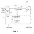
- FIG. 18is a block diagram showing a clock-generator architecture for a programmable-logic-based system on a chip according to the present invention.
- FIG. 19is a block diagram showing a more detailed view of the operation of an illustrative real time clock in the system on a chip of the present invention.
- system-on-a-chipgenerally refers to an integrated circuit device that includes multiple types of integrated circuits on a single die, where the circuits are of types that have traditionally been constructed on separate silicon wafers.
- FIG. 1An SOC 10 according to the present invention design is shown generally in a block-diagram architectural level drawing in FIG. 1 , which shows its main components.
- an illustrative embodiment of the present inventionis a system-on-a-chip integrated circuit 10 that includes a programmable logic block 12 , at least one non-volatile memory block 14 , analog ASIC circuit blocks 16 a through 16 f , digital ASIC circuit blocks 18 a through 18 f , digital input/output (“I/O”) circuit blocks 20 and analog I/O circuit blocks 22 .
- I/Odigital input/output
- System-on-a-chip integrated circuit 10also includes a system controller circuit block 24 and a clock circuit 26 .
- Programmable logic block 12may be an FPGA array.
- FPGA arraysare well known in the art, and it is contemplated for purposes of the present invention that any type of FPGA circuit block may be employed in the system-on-a-chip integrated circuit 10 of the present invention.
- the number of data inputs and outputs and the number of implementable combinatorial and sequential logic functionswill depend on the particular design of FPGA circuit used in the FPGA array. Persons of ordinary skill in the art will appreciate that other programmable logic blocks such as complex programmable logic devices (CPLD) and other programmable logic blocks may be used in the present invention.
- CPLDcomplex programmable logic devices
- Non-volatile memory block 14may be formed from an array of, as a non-limiting example, flash memory cells and a memory controller for the array. Flash memory cells are well known in the art and the present invention is not limited to use of any particular kind of flash memory cells or other non-volatile memory technology, such as nanocrystal, SONOS, solid-electrolyte switching devices, and other types as will be appreciated by persons of ordinary skill in the art. Persons of ordinary skill in the art will appreciate that, in some embodiments of the present invention, non-volatile memory block 14 may be segmented into a plurality of separately addressable arrays, each with its own memory controller. The number of data inputs and outputs and address inputs will depend on the size of the array used.
- Analog ASIC circuit blocks 16 a through 16 fare illustrated in FIG. 1 , although persons of ordinary skill in the art will observe that the provision of six analog ASIC circuit blocks 16 a through 16 f in FIG. 1 is merely illustrative and in no way limiting. Actual embodiments of system-on-a-chip integrated circuits according to the present invention may have an arbitrary number of analog ASIC circuit blocks. Analog ASIC circuit blocks 16 a through 16 f may alternatively be described as “hardwired,” “mask programmable,” or “ASIC” circuits or circuit blocks.
- analog blocksare also referred to as “analog peripherals,” and may include, as non-limiting examples, a digital-to-analog converter (DAC), an analog-to-digital converter (ADC), a Pulse Width Modulator (PWM), a MOSFET Controller, a Voltage Reference circuit, a Low-dropout (LDO) regulator, an Analog multiplexer (MUX), or an RF Transceiver.
- DACdigital-to-analog converter
- ADCanalog-to-digital converter
- PWMPulse Width Modulator
- MOSFET Controllera Voltage Reference circuit
- LDOLow-dropout
- MUXAnalog multiplexer
- RF TransceiverRF Transceiver.
- stand alone analog circuit blocks for more specific functionsmay be provided, as described above.
- a stand-alone hardwired current monitor, a stand-alone hardwired temperature monitor, or a stand-alone hardwired voltage monitormay be provided.
- Embedded analog peripheralsmay also be used to enhance generic microcontroller (“MCU”) functions with a programmable “soft” processor core programmed into the programmable logic block.
- MCUmicrocontroller
- the numbers and kinds of inputs and outputs of the individual analog ASIC circuit blocks 16 a through 16 fwill depend on the functional nature of the circuits employed.
- Digital ASIC circuit blocks 18 a through 18 fare illustrated in FIG. 1 , although persons of ordinary skill in the art will observe that the provision of six digital ASIC circuit blocks 18 a through 18 f in FIG. 1 is merely illustrative and in no way limiting. Actual embodiments of system-on-a-chip integrated circuits according to the present invention may have an arbitrary number of digital ASIC circuit blocks.
- Digital ASIC circuit blocks 18 a through 18 fmay comprise circuit blocks such as, but not limited to, state machines, analog sequencers, microprocessors, digital signal processors (“DSPs”). Hard digital blocks are especially useful to implement interfaces such as the interface between the programmable logic and the memory blocks on a device.
- the FPGA/Memory interfaceis described in more detail in the section describing the non-volatile memory controller.
- Hard digital blocksmay also be used to implement interfaces between the programmable logic or the memory blocks and hard analog blocks.
- a hard digital blockis used as a control block for the non-volatile memory block.
- the non-volatile memory controlleris described in more detail herein.
- Such digital blocksmay be implemented in a similar manner to the way in which such digital blocks are implemented in current application-specific integrated circuits (“ASICs”).
- ASICsapplication-specific integrated circuits
- all, or a portion of each of these types of blocksmay be implemented in programmable logic, sometimes referred to as “soft” implementations.
- softimplementations.
- the numbers and kinds of inputs and outputs of the individual digital ASIC circuit blocks 18 a through 18 fwill depend on the functional nature of the circuits employed.
- System-on-a-chip integrated circuit 10also includes digital I/O circuit blocks 20 .
- Digital I/O circuit blocks 20may comprise conventional digital I/O circuitry, such as that commonly employed in known FPGA and similar integrated circuits.
- System-on-a-chip integrated circuit 10also includes analog I/O circuit blocks 22 .
- Analog I/O circuit blocks 22may comprise any of the many analog amplifier circuits that are well known in the art.
- System-on-a-chip integrated circuit 10also includes a system controller circuit block 24 .
- a system controller circuit block 24provides master control functionality for the other blocks in the SOC device, including managing power up sequencing and inter-operation of the various components of the system on a chip.
- the system controller 24may control off-chip devices via signals output via the digital or analog I/Os of the device of the present invention such as reset and enable signals.
- the system controller 24includes various circuits for managing the different functions of the SOC device. In some embodiments, these circuits may all be implemented in hardwired circuit blocks, while in other embodiments, some of the circuits may be implemented in a portion of the programmable logic of the programmable logic block 12 .
- An advantage of implementing control functions in programmable logicis that the user is able to adapt the control functions to the user's application. This is especially useful if the user wishes to employ the programmable system on a chip device to control elements of the user's system that are outside the system on a chip device.
- the system controller 24 shown in FIG. 1includes a power-up control circuit, an analog power supply circuit, a voltage reference circuit, and a system supervisor circuit.
- the power-up control circuitincludes circuitry for managing the SOC device during power-up, as will be described in more detail below.
- System-on-a-chip integrated circuit 10also includes a clock circuit 26 .
- Clock circuit 26may include one or more clock sources and clock-signal-distribution systems. The number of such clocks provided on any system-on-a-chip integrated circuit fabricated according to the present invention is a matter of design choice. Such circuits and systems are well known in the art.
- the inputs and outputs of the various circuit elements of the programmable logic block 12 , a non-volatile memory block 14 , analog ASIC circuit blocks 16 a through 16 d , digital ASIC circuit blocks 18 a through 18 d , digital input/output (“I/O”) circuit blocks 20 and analog I/O circuit blocks 22 , system controller circuit block 24 and clock circuit 26may be connected together by a user by programmably connecting together their various inputs and outputs through a network of programmable interconnect conductors that is provided on the system-on-a-chip integrated circuit.
- FIG. 2A simplified diagram of a portion of an illustrative programmable interconnect architecture that may be employed with the system-on-a-chip integrated circuit of FIG. 1 is shown in FIG. 2 .
- FIG. 2illustrates a portion of an illustrative interconnect architecture. Persons of ordinary skill in the art will understand that FIG. 2 is largely schematic and simplified in nature, and in no way limits the present invention to the particular interconnect architecture depicted.
- an illustrative interconnect architecturethat can be implemented with the present invention may include interconnect conductors that run in horizontal and vertical directions in metal interconnect layers disposed over the surface of the silicon die comprising the system-on-a-chip integrated circuit 10 .
- Both the horizontal and vertical interconnect conductorsmay be segmented to allow versatility in forming interconnect between inputs and outputs of the various circuit elements disposed in system-on-a-chip integrated circuit 10 of FIG. 1 .
- the various interconnect conductorsmay be of varying lengths or may be segmented into varying lengths. In addition, either flat or hierarchical interconnect systems may be employed.
- the segments of the horizontal and vertical interconnect conductorsmay be programmably joined together by user-programmable interconnect elements indicated by the circled “X” symbols shown on FIG. 2 . Intersections formed by individual ones of the horizontal and vertical interconnect conductors may also be populated by user-programmable interconnect elements.
- the user-programmable interconnect elementsmay be in the form of one-time programmable antifuse elements as are known in the art, or may be in the form of reprogrammable switches as are also known in the art. The latter reprogrammable interconnect switches may employ technologies such as flash memory, SRAM, and other known interconnect switch technologies.
- a group 30 of segmented horizontal interconnect conductorsis shown crossing a group 32 of segmented vertical interconnect conductors to form intersections.
- the horizontal interconnect conductors and the vertical interconnect conductorsare disposed in different metal interconnect layers of the system-on-a-chip integrated circuit.
- An exemplary individual horizontal interconnect conductoris shown to be comprised of segments 34 a , 34 b , 34 c , and 34 d , each adjoining segment being coupled to one another by user-programmable interconnect elements 36 , 38 , and 40 , as shown in FIG. 2 .
- an exemplary individual vertical interconnect conductoris shown to be comprised of segments 42 a , 42 b , 42 c , and 42 d , each adjoining segment being coupled to one another by user-programmable interconnect elements 44 , 46 , and 48 , as also shown in FIG. 2 .
- Horizontal interconnect conductor segment 34 dis shown intersecting vertical interconnect conductor segment 42 b .
- the intersection of these two interconnect conductor segmentsis populated with a user-programmable interconnect element 50 .
- a conductive pathmay be formed between the output of one of the circuit elements on the system-on-a-chip integrated circuit and the input of another one of the circuit elements on the system-on-a-chip integrated circuit to form a connection therebetween.
- the illustrative interconnect architecture depicted in FIG. 2may appear more or less regular over areas such as the FPGA array of logic block 12 of FIG. 1 and may vary in density, pattern, and/or and direction over other areas and circuit blocks of the system-on-a-chip integrated circuit 10 of FIG. 1 as appropriate for the desired connection opportunities.
- FIG. 3is a block diagram of a system-on-a-chip integrated circuit 60 similar to the system-on-a-chip integrated circuit 10 shown in FIG. 1 , in that it includes a programmable logic block 62 , a non-volatile memory block 64 , analog ASIC circuit blocks 66 a through 66 f , digital ASIC circuit blocks 68 a through 68 f , digital input/output (“I/O”) circuit blocks 70 and analog I/O circuit blocks 72 , a system controller circuit block 74 and a clock circuit 76 .
- System-on-a-chip integrated circuit 60also includes a volatile memory block 78 (e.g., an SRAM block).
- the configuration shown in FIG. 3is simply suggestive of the feature set of a system-on-a-chip integrated circuit and is not intended to be limiting in terms of the number and distribution of circuit blocks, layout and other design-choice features.
- FIG. 4Another embodiment of an FPGA-based system-on-a-chip 80 is shown in FIG. 4 .
- the FPGA-based system-on-a-chip shown in FIG. 4includes a programmable logic block 82 , a non-volatile memory block 84 , analog ASIC circuit blocks 86 a through 86 f , digital ASIC circuit blocks 88 a through 88 f , digital input/output (“I/O”) circuit blocks 90 and analog I/O circuit blocks 92 , system controller circuit block 94 and a clock circuit 96 .
- the system-on-a-chip integrated circuit 80 of FIG. 4also includes SRAM block 98 .
- Flash memory block 84 and SRAM block 98are large enough to allow full use of the microprocessor.
- An example of such an embodimentmay include a microprocessor such as an 8051 hardwired core (a popular 1970's 8-bit microprocessor with a 16-bit address space) with 64 K-bytes of SRAM and 64 K-bytes of flash memory.
- memory blocks that are not used by the processorcould be allocated for use by the FPGA block 82 of the circuit.
- a more sophisticated microprocessor or microcontrollermay be provided.
- the SRAMmay operate under DMA mode for the microprocessor.
- An FPGA or other programmable logic deviceincluding a microprocessor (soft or hard) requires memory for program store. When program-storage memory is static, an on-board PROM program-store block is useful for this task.
- PROM memoryhas an advantage as it is much denser than SRAM and does not need to be loaded from some external source.
- the PROMhowever may be quite slow, so a SRAM cache may be provided for the fast processor into which the PROM program-store is loaded (perhaps in parallel or in the background) such that the entire PROM would not need to be duplicated in SRAM.
- SRAM cachemay be provided for the fast processor into which the PROM program-store is loaded (perhaps in parallel or in the background) such that the entire PROM would not need to be duplicated in SRAM.
- SRAM-based FPGAis typically configured by a bit-stream that is stored in non-volatile memory, by integrating a microcontroller and flash FPGA in one chip,
- the microcontrollercan take control of FPGA re-configuration for certain applications during boot-up or on-the-fly system operation.
- the configuration procedurecan be reversed to let the FPGA set up the microcontroller, for example, if the system times out or hangs during operation, the FPGA can send a soft reset to the microcontroller instead of requiring a hard reset.
- Both the microcontroller and FPGA blocksshare on-chip SRAM, which can be designed as dual-port SRAM to be accessed synchronously.
- on-chip SRAMcan work under DMA mode for the microcontroller.
- Customized instructionscan be implemented in flash memory, or FPGA blocks can be reconfigured as a co-processor either through the on-chip microcontroller or external host to build a powerful flash-based FPGA on-chip processor platform.
- One particular embodiment of the inventionmay be configured using a highly successful flash FPGA architecture as the programmable logic block 12 of FIG. 1 .
- An example of such an architecturemay be found in the ProASIC line of FPGA integrated circuits available from Actel Corporation of Mountain View, Calif.
- system-on-a-chip devices according to the present inventiondramatically simplify system design, and as a result, save both board space and overall system cost.
- the state-of-the-art flash memory technologyoffers very high-density integrated flash arrays and therefore a substantial cost saving over use of external flash chips to configure SRAM-based FPGAs, the traditional alternative.
- the multiple analog circuit blocksextend the traditional FPGA application from the purely digital domain to mixed-signal applications.
- the embedded flash memory and integrated analog circuit blockscan be used with an integrated soft (i.e., configured from programmable logic) processor to implement a full functional flash microcontroller unit (MCU), or the advanced analog circuit blocks can be used with high speed FPGA logic to offer system and power supervisory abilities.
- MCUflash microcontroller unit
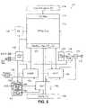
- SOC 110includes a field-programmable gate array (FPGA) that includes an FPGA core 112 comprising logic tiles, routing, and flash-cell switches and programming structures and techniques as is known in the art.
- FPGAfield-programmable gate array
- GPIOGeneral-purpose input/output circuits 116 may be coupled to the FPGA core 112 through I/O tiles 114 as is known in the art.
- a clock generator circuits block 118 and distribution systemis included to provide an on-chip source for clock signals.
- the clock generator circuits block 118may include RC oscillators.
- One or more of these moderate precision (1-2%) clock sourcesmay be completely contained within the SOC 110 and may be used for internal charge pumps and NVM erase/program timing. They can also be the source of clocks for the FPGA and/or the external system where precise frequency control is not needed.
- the clock generator circuits block 118 in SOC 110 of the present inventionmay also include a crystal oscillator circuit. This relatively high-precision clock source ( ⁇ 100 PPM) requires an inexpensive external crystal that may be connected to the SOC 110 through a pair of I/O pins as shown in FIG. 5 .
- the clock-generator circuits block 118can be used for all FPGA and system clock requirements.
- the SOCmay further include one or more phase locked loops (PLLs) 120 .
- PLLsphase locked loops
- clock generator 118 of the SOC 110 of FIG. 5may also include a glitchless clock multiplexer to allow clean switching between multiple internal or external clock sources.
- the glitchless clock multiplexermay be used to provide a selectable low power (low frequency) mode to on-chip clocked systems, or to switch between clocks for any other application reason. This can save board space in a system in which the SOC is used and provides a reliable clock source for critical system management functions.
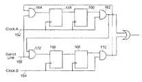
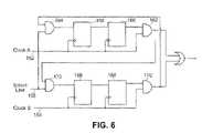
- An illustrative clock multiplexerwill be described with reference to FIG. 6 .
- a flash programming circuit 122 for programming the FPGAis coupled to a JTAG TAP controller 124 , designed in accordance with the JTAG standard, for entering the programming data through a JTAG port 126 to define the configuration of the FPGA circuits as is known in the art.
- a security circuit implementing an encryption/decryption algorithmmay be provided.
- decryption circuit 128may be a circuit designed to implement the AES encryption/decryption standard.
- AESAdvanced Encryption Standard
- NISTNational Institute of Standards and Technology
- NTISNational Technical Information Service
- the Advanced Encryption Standardspecifies a cryptographic algorithm that can be used to protect electronic data.
- the AES algorithmis a symmetric block cipher that can encrypt (encipher) and decrypt (decipher) information.
- the AES algorithmis capable of using cryptographic keys of 128, 192, and 256 bits to encrypt and decrypt data in blocks of 128 bits.
- the algorithm specified in this standardmay be implemented in software, firmware, hardware, or any combination thereof. The specific implementation may depend on several factors such as the application, the environment, the technology used, etc. Encryption can be used to protect the FPGA configuration information, the contents of the non-volatile memory, etc.
- GPIO circuits that would normally be disposed along the lower edge of the FPGA coreare shown replaced in FIG. 1 by internal interface circuits 130 for making connections between the FPGA core 112 and the other SOC circuit blocks.
- these GPIO circuits and interface blocksmay be in the form of “tiles” having identical footprints.
- SOC 110also includes at least one non-volatile memory (NVM) block.
- NVMnon-volatile memory
- the flash memory arraysare preferably sized between about 64 kBytes to about 512 Kbytes.
- Each of flash memory arrays 132 and 134has built-in known charge pumps and programming circuits to allow each to operate independently from the other and from the FPGA core.
- the provision of more than one flash memory blockpermits the SOC 110 of FIG. 5 to simultaneously perform two separate system functions using non-volatile memory.
- timing inputis provided to the flash memory blocks from the on-chip clock generator circuits 118 for accurate/reliable programming and erase of each flash memory array 132 and 134 .
- NVM programming paths for NVM blocks 132 and 134including through the FPGA from data sources in the FPGA core 112 , through the FPGA core from data sources outside the FPGA core 112 through the GPIO 116 , directly from the JTAG port 124 from external JTAG masters (such as an FPGA programmer), and data streams decrypted by the AES block 126 from JTAG data sources.
- the FPGA to NVM module interfaceprovides JTAG full capture and control boundary scan register functionality.
- a boundary scan registercan directly control and capture all core to NVM inputs and can capture all NVM outputs in a manner known in the boundary-scan art.
- the NVM blocks 132 and 134can be used to store data appropriate to provide power-up initialization of FPGA memories, analog-to-digital converter (ADC) sequencing and configuration data, system-wide power up parameters, program storage for microcontrollers or microprocessors, and general data storage as is known in the art.
- ADCanalog-to-digital converter
- the SOC 110 of FIG. 5also includes an ADC 136 .
- the ADCmay select from one of a plurality of multiplexed analog inputs and converts the applied voltage to an equivalent digital value.
- the ADCmay also include selectable conversion resolution (e.g., 8, 10, or 12 bit conversion).
- a voltage reference input at the input of ADC 136corresponds to full-scale output.
- ADC 136may include a multiplexer coupled to its input to allow multiple analog voltage sources to be used.
- the ADC 136is coupled to analog I/O 138 .
- Analog I/O 138is also coupled to interface tiles 130 as will be more fully disclosed herein.
- the SOC 110 of FIG. 5also includes a system supervisor master block 140 .
- System supervisor master block 140includes an on-chip power up control block 142 , analog voltage supply charge pumps 144 , an on-chip voltage reference 146 and a system supervisor block 148 .
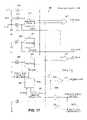
- Glitchless clock multiplexer 150may be used to select between a “Clock A” input at line 152 and a “Clock B” input at line 154 by use of a select line 156 .
- the clock A input 152drives the clock inputs of data latches 158 and 160 and one input of AND gate 162 .
- Select line 156is coupled to one input of an AND gate 164 whose output drives the data input of data latch 158 .
- the clock B input 154drives the clock inputs of data latches 166 and 168 and one input of AND gate 170 .
- the data output of data latch 168drives the other input of AND gate 170 .
- Select line 156is coupled to one (inverted) input of an AND gate 172 whose output drives the data input of data latch 166 .
- the output of AND gate 170drives the other (inverted) input of AND gate 164 and the output of AND gate 162 drives the other (inverted) input of AND gate 172 .
- the outputs of AND gates 162 and 170drive inputs of OR gate 174 .
- Persons of ordinary skill in the artwill observe that the circuit of FIG. 6 allows selecting between the clock inputs A and B without producing any glitches at the output of OR gate 174 .
- analog I/O circuits 138 in FIG. 5are used to provide inputs and outputs to ADC 136 .
- analog I/O functionsmay be grouped into sets.
- Analog I/O circuits 138may contain a number of these sets.
- the set of analog I/O circuits shown in FIG. 7has four members. Persons of ordinary skill in the art will realize that FIG. 7 is illustrative only, and a set of analog I/O circuits in an actual SOC may have fewer or more members.
- a first member 180 of the setmay be a voltage input block coupled to I/O pad 182 .
- I/O pad 182that may either have a direct connection to the input of ADC 136 (or one input of its input multiplexer), or may be connected to it through a buffered prescaler circuit 184 .
- Prescaler circuit 184may have a programmable gain set to 1 of n selectable values as will be disclosed further herein.
- Multiplexer 186is employed to select between the direct input or the prescaled input.
- the select inputs of multiplexer 186may be controlled from the FPGA.
- I/O pad 182can be configured through digital input circuit 188 as a low-performance digital input to the FPGA core.
- a second member 190 of the setmay be a current-monitor input block coupled to I/O pad 192 .
- I/O pad 192may either have a direct connection to the input of ADC 136 (or one input of its input multiplexer), or may be connected to it through a buffered prescaler 194 .
- prescaler 194may have a programmable gain set to 1 of n selectable values as will be disclosed further herein.
- Multiplexer 196is employed to select between the direct input from I/O pad 192 or the prescaled input. The select inputs of multiplexer 196 may be controlled from the FPGA.
- I/O pad 192can be configured through digital input circuit 198 as a low-performance digital input to the FPGA core.
- set member 190may be used to measure the difference between I/O pad 182 and 192 . This may be used to measure a voltage drop across a small resistor in series with an external power supply.
- I/O pad 192is connected to one input of an amplifier 160 .
- the other input of amplifier 198is coupled to I/O pad 182 .
- the output of amplifier 160is presented to a third input of multiplexer 194 . If a low value (e.g., 0.1 ohms) resistor (not shown in FIG.
- a third member 210 of the setmay be a temperature-monitor input block coupled to I/O pad 212 .
- I/O pad 212may either have a direct connection to the input of ADC 136 (or one input of its input multiplexer), or may be connected to it through a buffered prescaler 214 .
- prescaler 214may have a programmable gain set to 1 of n selectable values as will be disclosed further herein.
- Multiplexer 216is employed to select between the direct input from I/O pad 210 or the prescaled input. The select inputs of multiplexer 216 may be controlled from the FPGA.
- I/O pad 212can be configured through digital input circuit 218 as a low-performance digital input to the FPGA core.
- set member 210may be used as a temperature monitor for a signal on I/O pad 212 .
- This set member 210may be configured to measure temperature of an external diode by taking advantage of the temperature behavior of the I-V characteristics of a diode.
- a temperature monitor circuit 220may also be coupled to an input of multiplexer 216 .
- the SOC of the present inventionmay be supplied with a plurality of temperature monitor circuits. According to one embodiment of the invention, a number of temperature sensors are for measuring external temperature (e.g., the junction temperatures of other ICs or air temperature) and one for measuring its own junction temperature. Temperature monitor circuit 220 is explained in more detail with reference to FIG. 10 .
- a fourth member 230 of the setmay be a gate-driver output block coupled to I/O pad 232 .
- Power MOSFET gate driver circuit 234drives I/O pad 232 from the FPGA.
- I/O pad 232may be coupled to I/O pad 232 and/or I/O pad 212 through either of pull-up resistors 236 and 238 , respectively.
- resistors 236 and 238are optional.
- An optional ramp resistor 200may be coupled to I/O pad 232 or I/O pad 212 .
- Gate driver circuit 234is explained in more detail with reference to FIG. 11 .
- the pre-scaler circuits 184 , 194 , and 214are provided to scale external voltages up or down.
- a pre-scaler circuitis shown that can scale external voltages by one of eight factors.
- the pre-scaler circuitcan be used in voltage monitor functions or in any analog input functions.
- the pre-scaler circuitmay be based upon a current mirror circuit.
- a first side of the current mirror circuitincluding a resistor 250 coupled between I/O pad 192 and diode-connected n-channel MOS transistor 252 .
- the gate and drain of diode-connected n-channel MOS transistor 252are connected to the gates of n-channel MOS transistors 254 , 256 , 258 , and 260 .
- the ratios of the width of diode-connected n-channel MOS transistor 252 to the widths of n-channel MOS transistors 254 , 256 , 258 , and 260are selected to produce the desired scaling factors.
- n-channel MOS transistors 254 , 256 , 258 , and 260are coupled to a fixed potential, such as ground, through enable n-channel transistors 262 , 264 , 266 , and 268 , respectively.
- the gates of enable n-channel transistors 262 , 264 , 266 , and 268are driven from a decoder circuit 310 .
- the control lines of decoder circuit 310are driven from the FPGA array.
- the drains of n-channel MOS transistors 254 , 256 , 258 , and 260are coupled together to the non-inverting input of operational amplifier 312 . Resistor 314 sets the gain of operational amplifier 312 .
- the following voltage-scaling factors0.20161, 0.40322, 0.80645, 1.6129, 3.2258, 6.45161, 12.90322, and 25.80645 have been found to be particularly useful. This is particularly useful where the full-scale voltage of ADC 136 of FIG. 5 is 3.3V.
- the pre-scalercan scale negative voltages to positive voltages (i.e.
- ⁇ 16Vcan be converted to 3.3V).
- the function of the pre-scaleris to convert input voltages into ranges that are acceptable by the ADC.
- the reason for employing the exemplary scaling factors recited hereinis for user convenience to achieve correspondence between the digital output of the ADC and one-millivolt steps. From an examination of this disclosure, persons of ordinary skill in the art will appreciate that any number of different scaling factors may be selected.
- FIG. 8An illustrative configuration for amplifier 200 of FIG. 7 is shown and described with reference to FIG. 8 .
- External resistor 280is shown coupled between I/O pads 142 and 192 .
- the offset value of the operational amplifier 290is stored in capacitor 292 so that the output of the operational amplifier 250 is approximately at ground.
- the capacitors 294 and 296are charged to the voltage level which is at the right side of the external resistor 280 and the non-inverting input of the operational amplifier 290 is at ground.
- the inverting input of operational amplifier 290is at virtual ground.
- Switches 282 , 284 , 286 , and 288are then switched in order (first switch 282 , then switch 284 , then switch 286 , then switch 288 ). After all the switches 282 , 284 , 286 , and 288 are at their new positions, the voltage drop across the external resistor 280 is amplified by the operational amplifier 290 with a gain defined by (C 256 +C 258 )/C 258 . The output voltage of the operational amplifier 290 is applied to the input of the ADC. Since the value of the external resistor value is known, the current through the external resistor is known. The configuration of the circuit of FIG. 9 has the advantage of avoiding amplifying the voltage offset of operational amplifier 290 .
- temperature monitor circuit 220is explained in more detail. This circuit forces two different currents through a diode and measures the voltage drop difference across the diode. It then amplifies this voltage by a factor of five and sends it to the ADC. This amplified voltage difference directly corresponds to temperature (in ° K.).
- a voltage difference of 59.6 mV(corresponding to diode temperature of 25° C.) is measured by sequentially forcing 10 uA and 100 uA across diode 300 . This is amplified 5 ⁇ —which gives 298 mV—which corresponds to 298K (25 C).
- Diodeis coupled to I/O pad 212 .
- Two current-generating circuitsare shown, allowing the diode 300 to be oriented in either direction.
- the first current-generating circuit which sources currentincludes a first leg including p-channel MOS transistors 302 , 304 , and 306 coupled in series between a supply potential of +3.3 VDC and the I/O pad 212 .
- the gate of transistor 302is coupled to a positive bias potential.
- the gate of transistor 304is coupled to ground and the gate of transistor 306 is coupled to a Source/Sink control signal.
- the sizes of transistors 302 , 304 , and 306 and the value of the positive bias potentialare chosen to cause 10 ⁇ A to flow (source) through diode 300 .
- the second leg in the first current-generating circuitincludes p-channel MOS transistors 308 , 310 , and 312 coupled in series between the supply potential of +3.3 VDC and the I/O pad 212 .
- the gate of transistor 308is coupled to the positive bias potential.
- the gate of transistor 310is coupled to a control signal “S” and the gate of transistor 312 is coupled to the Source/Sink control signal.
- the sizes of transistors 308 , 310 , and 312 and the value of the positive bias potentialare chosen to cause an additional 90 ⁇ A to flow (source) through diode 300 .
- the second current-generating circuit which sinks currentincludes a first leg including n-channel MOS transistors 314 , 316 , and 318 coupled in series between a supply potential of ⁇ 3.3 VDC and the I/O pad 212 .
- the gate of transistor 314is coupled to a negative bias potential.
- the gate of transistor 316is coupled to a positive voltage and the gate of transistor 318 is coupled to the Source/Sink control signal.
- the sizes of transistors 314 , 316 , and 318 and the value of the negative bias potentialare chosen to cause 10 ⁇ A to flow (sink) through diode 300 .
- the second leg in the first current-generating circuitincludes n-channel MOS transistors 280 , 282 , and 284 coupled in series between the supply potential of ⁇ 3.3 VDC and the I/O pad 212 .
- the gate of transistor 280is coupled to the negative bias potential.
- the gate of transistor 282is coupled to the control signal “S” and the gate of transistor 284 is coupled to the Source/Sink control signal.
- the sizes of transistors 280 , 282 , and 284 and the value of the negative bias potentialare chosen to cause 90 ⁇ A to flow (sink) through diode 300 .
- the Source/Sink control signalis low, the current sourcing transistors operate. If the Source/Sink control signal is high, the current sinking transistors operate. In either case, the first leg of the circuit (either transistors 302 , 304 , and 306 or transistors 314 , 316 , and 318 ) are turned on, sourcing or sinking 10 ⁇ A through diode 300 . When the “S” (or “S!”) signal is asserted, the second leg of the circuit (either transistors 308 , 310 , and 312 or transistors 320 , 322 , and 324 ) is also turned on, sourcing or sinking a total of 100 ⁇ A through diode 300 .
- the remaining components of the circuitinclude operational amplifier 326 having its non-inverting input grounded, capacitor 328 coupled between I/O pad 212 and the inverting input of operational amplifier 326 , and capacitor 330 , coupled between the inverting input of operational amplifier 326 and its output through n-channel MOS transistor 332 .
- capacitor 328has five times the capacitance of capacitor 330 , which determines the gain of the circuit. Capacitor 330 stores and thus cancels the offset of operational amplifier 326 .
- the common connection of capacitor 330 and transistor 332is coupled to ground through n-channel MOS transistor 334 .
- the gate of transistor 332is coupled to a control signal Y! and the gate of transistor 334 is connected to a control signal Y.
- An n-channel MOS transistor 336is coupled between the inverting input sand the output of operational amplifier 326 and has its gate coupled to a control signal X.
- An n-channel MOS transistor 338is coupled to the inverting input of operational amplifier 326 and has its gate coupled to a control signal X!.
- the relative timing of the control signals X, Y, Y! and Sis shown at the right side of FIG. 10 .
- the difference in diode voltage before and after the timing sequenceis amplified by the circuit gain and appears at the output of the operational amplifier 326 , corresponding to the absolute temperature.
- External power MOSFET 340has its source coupled to supply potential 342 . Its gate is coupled to I/O pad 232 and its drain is coupled to I/O pad 212 or 192 (see FIG. 7 ). If supply potential 342 is positive, power MOSFET 340 will be a p-channel device and if supply potential 342 is negative, power MOSFET 340 will be an n-channel device. Resistor 236 or 238 (again see FIG. 7 ) may be disposed in the SOC device and is used to assure that the power MOSFET 340 will be turned off unless a gate drive signal is supplied at I/O pad 232 .
- Operational amplifier 344drives the gate of p-channel MOS gate-drive transistor 346 .
- the drain of p-channel MOS gate-drive transistor 346is coupled to I/O pad 232 .
- the source of p-channel MOS transistor gate-drive 346is coupled to a positive supply potential through p-channel MOS enable transistor 348 .
- the non-inverting input of operational amplifier 344is coupled to the drain of power MOSFET 340 via I/O pad 192 (or 212 ) through resistor 350 .
- the inverting input of operational amplifier 348is coupled to capacitor 352 driven by constant-current source 354 .
- operational amplifier 356drives the gate of n-channel MOS gate-drive transistor 358 .
- the drain of n-channel MOS gate-drive transistor 358is coupled to I/O pad 232 .
- the source of n-channel MOS transistor gate-drive 358is coupled to a negative supply potential through n-channel MOS enable transistor 360 .
- the inverting input of operational amplifier 356is coupled to the drain of power MOSFET 340 via I/O pad 192 (or 212 ) through resistor 340 .
- the non-inverting input of operational amplifier 356is coupled to capacitor 362 driven by constant-current source 364 .
- the non-inverting input of operational amplifier 344 and the inverting input of operational amplifier 356are coupled to ground through resistor 366 .
- p-channel enable transistor 348is turned on.
- current source 354is turned on and charges capacitor 352 at a linear rate.
- the voltage on capacitor 352is amplified with a negative gain, producing a decreasing ramp voltage at the output of operational amplifier 348 .
- Thiscauses a decreasing ramp voltage at the drain of p-channel gate drive transistor 346 to turn on p-channel MOS power transistor 340 .
- the final gate voltage on the MOS power transistor 340is established by the IR drop across the gate-to-source resistor 236 or 238 and is determined by the current through the p-channel enable transistor 348 .
- n-channel enable transistor 360is turned on, current source 364 is turned on and charges capacitor 362 at a linear rate.
- the voltage on capacitor 362is amplified with a positive gain, producing an increasing ramp voltage at the output of operational amplifier 356 . This causes an increasing ramp voltage at the drain of n-channel gate drive transistor 358 to turn on the p-channel MOS power transistor.
- the feedback provided to the operational amplifiers 344 and 356 through resistor 350assures controlled ramp rates on the load.
- FIG. 12illustrative embodiments of internal interface circuits 130 ( FIG. 5 ) that are particularly useful for the SOC of the present invention are shown. Persons of ordinary skill in the art will observe that the circuits shown in FIG. 12 are illustrative only and not limiting. Such skilled persons will appreciate that other interface circuits may be used.
- Internal interface circuit 130may include a plurality of “tiles”, each having a plurality of different types of interface circuits.
- a “tile”is a layout subunit where the inputs and outputs are placed in the same physical locations to allow for modular chip design. More than one of each type of circuit may be included in each tile, the exact number of each being a matter of design choice.
- a pair of buffers 370 and 372may be provided. Buffers 370 and 372 are shown in FIG. 12 having their inputs coupled together and having their outputs independently connectable. Buffers 370 and 372 act as input buffers for the FPGA core.
- Internal interface circuit 130may also include inverting buffer 374 disposed between an input node 376 and an output node 378 .
- a first programmable element 380is coupled between the input of buffer 374 and the output node 378 .
- a second programmable element 382is coupled between the output of buffer 374 and the output node 378 .
- programmable element 380is programmed and programmable element 382 is left unprogrammed, connecting input node 376 directly to output node 378 .
- programmable element 382is programmed and programmable element 380 is left unprogrammed, coupling input node 376 to output node 378 through buffer 374 .
- Buffer 374acts as an output buffer for the FPGA core.
- a pair of programmable elements 384 and 386may be connected in series between a logic-high voltage potential and a logic-low voltage potential.
- the common connection between these programmable elementsis used as an output node 388 to drive, for example, the gate of transistor 348 or 360 in FIG. 11 , or at least one of the control lines of multiplexers 186 196 216 of FIG. 7 .
- power for the analog portion of the ADC 136may be 3.3V.
- the analog I/O circuitsmay also employ a +/ ⁇ 3.3V supply. These supply voltages may be generated on chip from the 1.5V V CC power supply using charge pump circuits in a manner known in the art. Alternatively, 3.3 volts may be supplied to the SOC and 1.5 volts may be generated on chip by regulating down from the 3.3 volts.
- a high-precision voltageis needed as a reference voltage input to the ADC 136 or may be generated within the ADC 136 .
- This voltagemay be scaled from an on chip Bandgap voltage source using known techniques.
- Such a bandgap referenceis shown in FIG. 13 .
- a first grounded-base PNP transistor 390has a resistor 392 coupled between its emitter and the output of operational amplifier 394 .
- a second grounded base pnp transistor 396has a pair of resistors 398 and 400 coupled between its emitter and the output of operational amplifier 394 .
- the emitter of transistor 390is coupled to the non-inverting input of operational amplifier 394 and the common connection of resistors 398 and 400 is coupled to the inverting input of operational amplifier 394 .
- the output voltage V ref of the operational amplifier 394is given by the expression shown in FIG. 13 .
- a separate power source for the bandgap referenceis useful for reducing the risk of coupling noise from FPGA sources.
- the output of the bandgap referencemay also be used for controlling the level of on-chip generated analog supplies.
- the output of the bandgap referencemay be supplied to the non-volatile memory (NVM) blocks if the particular NVM being used requires a stable reference voltage (e.g., for the sense amplifiers).
- the bandgap reference circuitis used to generate a reference voltage that will be used by other analog blocks as well as the ADC 136 of FIG. 5 .
- the operational amplifier 394is not necessarily but advantageously powered by a 3.3V charge pump. Although the V ref output of the circuit is voltage-, process-, and temperature-independent, the minimum voltage supply required by the operational amplifier is about 1.35V. Hence it is preferably supplied by a 3.3V charge pump and not by 1.5V V CC .
- ADC 136 of FIG. 5is shown in more detail.
- ADC 136may be a capacitor-based successive approximation (SAR) ADC as is known in the art.
- the ADC 136is divided into two portions, an analog portion 410 and a digital portion 412 .
- the analog portion 410contains an analog multiplexer 414 , capacitor array 416 and a comparator 418 .
- the digital partcontains successive approximation register 420 , clock divider 422 , and conversion control logic 424 .
- calibration logic 426is coupled to a calibration capacitor array 428 .
- the analog multiplexer 414chooses one out of 32 input channels. Once a channel is selected using the multiplexer select lines, it charges the main capacitor array 416 during the sample phase. After that the sampled input that charged the capacitor array is compared to a known voltage and based on the compare result the capacitors are switched according to the successive approximation algorithm. When the two inputs of comparator 418 are equal, the data in the successive approximation register 420 is the digital equivalent of the analog input. Clock divider and sample time (which are programmable) determine the speed of this conversion.
- system supervisor master 140is intended to provide all chip-level and system level power-on/initialization/reset functions.
- the power-up control circuitincludes circuitry for managing the SOC device during power-up, as will be described in more detail below.
- the analog power supply circuitrymay include known power supply and management circuits, for supplying the required voltages for operation of the various circuit blocks of the SOC device, as well as different voltages for programming the programmable elements of the SOC device.
- the programmable logic block and digital hardwired blockshave their own power supply circuits separate from the system controller circuit block.
- the system controller circuitdoes include an analog power supply circuit block 144 .
- the analog power supply circuit block 144supplies power to the analog blocks as well as performing power monitoring functions for monitoring the power input to all blocks on the SOC device.
- the analog power supply circuitryincludes voltage monitoring circuits, charge pumps, and voltage supply circuitry. These types of circuits are all known in the art and are used on other types of semiconductor devices, such as ASICs.
- the analog power supply circuitry 144includes a voltage conversion and supply circuit block that may include, for example, voltage reference circuits, charge pumps, switching supplies, switch regulators, buck/boost regulators, and voltage regulators. Use of such circuits is known by those skilled in the art. Different circuit blocks in the SOC device may require different voltages, and these voltages may be different from the voltage supplied by the system of which the SOC device is a part. The voltage conversion and supply circuitry may be implemented, therefore, to provide the required power to the various components, as is known in the art. Once the voltage input to the device has been stepped up or stepped down, if required, via the circuits discussed above, the required voltages are provided to the various components of the SOC device via hardwired power lines.
- the voltage input to the devicemay be 3.3V, but the hardwired analog circuit blocks may require 1.5V so the voltage conversion and supply circuitry steps the device input voltage (V CC ) down to 1.5V in order to supply the digital circuits with the proper voltage.
- V CCdevice input voltage
- 1.5 voltscould be supplied to the SOC and pumped up to 3.3 volts.
- other elements of the SOCsuch as the programmable logic block and the non-volatile memory block have separate voltage conversion and supply circuitry that is not included in the system controller circuit block.
- the analog power supply circuitry 144also includes a voltage monitoring circuit for comparing an input voltage to a reference voltage, as is known in the art.
- the voltage monitoring circuitreceives a voltage reference signal (e.g., a bandgap reference signal from a voltage reference circuit, described below) as an input and uses it to compare other voltage supplies (e.g., the programmable logic block voltage supply, the non-volatile memory voltage supply, and the analog voltage supply) on the SOC device to the bandgap reference. If the voltages of the monitored supplies do not compare favorably with the reference voltage (i.e., are outside a predetermined error range), the voltage monitoring circuit may output a signal indicating the problem.
- the output error signalcould be used to delay start-up, trigger power down, generate one or more resets, assert an interrupt, or shut down operation of the SOC device.
- a voltage reference circuit 146 included in the system controller circuitmay be, for example, a bandgap reference circuit like the one described previously with reference to FIG. 13 , or other type of circuit known in the art for supplying an accurate reference voltage.
- a bandgap reference circuitprovides an absolute voltage output for reference by other circuits on the SOC device. Other power supplies can be compared to the reference voltage, as described above.
- the voltage reference circuit 146may include other circuitry, for example, operational amplifiers and buffers to change the level of the voltage.
- Bandgap voltage reference circuits other than the one illustrated in FIG. 13may be used in other embodiments of the invention, such as, for example a bandgap voltage reference circuit available from QualCore Logic, Inc, of Sunnyvale, Calif.
- This bandgap voltage reference circuitmay be separate from the general bandgap voltage source used for other circuit blocks on the SOC device, such as the programmable logic block, in order to provide a high-precision voltage input for components such as the ADC circuit, and to reduce the risk of coupling noise from other circuits.
- the power-up control circuit 142controls the internal power-up sequence of the SOC device.
- the power-up sequenceis used to insure that circuits receive the proper initialization, in the proper order, as power is supplied to the device.
- a typical power-up sequenceis shown in the state-machine diagram of FIG. 15A . Use of such a sequence reduces the chance for errors or damage to the SOC device resulting from circuits operating at an improper voltage (e.g., insufficient voltage or excessive voltage due to a spike) or to an improper sequence (e.g., an active circuit trying to communicate with a circuit that is not yet initialized.
- the power-up control circuit 142includes circuits that determine whether sufficient voltage is present to activate a circuit during power-up. These circuits can also be used to monitor the same voltages during operation of the SOC device, in addition to monitoring voltages during power-up.
- a timing diagram showing a typical startup sequenceis shown in FIG. 15B .
- a power-up control circuit 142 implementing a power-up sequence such as the example described hereinmay be implemented in hardwired circuitry, or a combination of hardwired circuitry and programmable logic.
- regulator circuits, charge pumps, voltage reference generators, etc.must be implemented in hardwired circuits, while sequence and control circuits may be implemented in hardwired circuits or programmed in programmable logic, as long as they are not required to be used before the programmable logic block is active.
- the power-up control circuit 142is shown to be comprised of circuits employing standard circuit elements to provide signals to activate various elements of the SOC device when the proper conditions are met (e.g., timing, sufficient voltage, etc.).
- the power-up control circuitincludes a voltage-reference-good circuit 440 for indicating that the circuit supplying the reference voltage is active and functioning within predetermined parameters.
- the power-up control circuitalso includes circuits 442 and 444 for indicating that each voltage supply (3.3V and 1.5V, in the example shown) is good (meaning active and functioning within predetermined parameters).
- the power-up control circuitmay also include voltage filter circuits for filtering voltages supplied to various components of the SOC device, such as, for example, the Vdd filter circuit 446 shown in FIG. 16 .
- the power-up control circuitincludes circuitry for activating various components of the SOC device such as the programmable logic block (circuit 448 ) and the non-volatile memory block (circuit 410 ), determining whether the component has become active, and outputting a signal to indicate that the circuit has become active. The signal indicating that a component is active may be used to activate the next step in the power-up sequence. Also shown in FIG. 16 are circuits for managing the power-up functions of the ADC. Specifically, the ADC-reference-good circuit 412 indicates that the reference voltage input to the ADC is accurate, and ADC-calibrate circuit 414 to indicates that the ADC is calibrated.
- circuits used in actual embodiments of the present invention embodimentswill depend on the particulars of the programmable logic, memory, analog, and digital hardwired blocks employed in the particular device.
- Examples of standard circuits that may be adapted to perform the power-up control functionsare multiplexers, control circuits, power monitor circuits, crystal oscillators, bandgap reference circuits, operational amplifiers, instrument amplifiers, charge pumps, filters, power supply regulators, known in the art and available from circuit design and IP licensing companies such as QualCore Logic, Inc., Sunnyvale, Calif.; TriCN, Inc., San Francisco, Calif.; or SliceX, Inc., Salt Lake City, Utah.
- FIG. 17shows a portion of the power-up control circuit 460 for performing functions early in the power-up sequence. Also shown in FIG. 17 is the voltage reference (bandgap) circuit of FIG. 13 in communication with the power-up circuits.
- the power-up circuits shown in FIG. 17are a 1.5 volt regulator circuit 462 for supplying 1.5 volts to the digital circuitry of the SOC device, a ⁇ Ve charge pump circuit 464 for supplying a negative voltage for the hardwired analog circuits of the SOC device, and a Vdd filter circuit 466 for providing a filtered 3.3 volt source to circuits requiring a filtered voltage (e.g., the bandgap voltage regulator circuit).
- 3.3Vis supplied to the SOC through I/O pad 468 and is supplied to 1.5 volt regulator circuit 462 as shown.
- I/O pad 468is also coupled to ⁇ Ve charge pump circuit 464 and to Vdd filter circuit 466 .
- the 1.5V output of 1.5 volt regulator circuit 462drives the base of external emitter-follower NPN transistor 470 through I/O pad 472 .
- the output of the external transistor 470is fed back to 1.5 volt regulator circuit 462 via I/O pad 474 .
- Comparator 476produces the 3.3V supply good signal when the voltage on I/O pad 474 is above the value set by the voltage from the 1.5 volt regulator 462 .
- Comparator 478produces the 1.5V supply good signal when the voltage on I/O pad 474 is above a preset value derived from the voltage at I/O pad 474 .
- ⁇ Ve charge pump circuit 464is presented at I/O pad 480 and the output of Vdd filter circuit 466 is presented at I/O pad 482 .
- the first signal produced in the power-up sequenceis the bandgap-good signal.
- This signalindicates that the bandgap reference circuit is outputting the accurate, regulated voltage for which it is designed. Since this voltage is the reference for the other circuits on the device, it is the first required to be operational during power-up.
- the reference voltage for the deviceis generally below the input voltage (Vcc) of the SOC device.
- the reference voltage for the SOC devicemay be 1.2V where Vcc for the SOC device is 3.3 volts.
- the portion of the power-up control circuit shown in FIG. 17also includes a threshold p-channel MOS transistor 484 and a small current source 486 for indicating when the bandgap reference circuit 488 is outputting the correct bandgap output voltage.
- the bandgap circuit 488receives a voltage input from the Vdd filter circuit 466 and outputs a controlled voltage via an output 490 .
- the source of threshold transistor 484is coupled to the Vdd filter circuit output, and a buffer 500 and the current source 486 are connected to the drain of threshold transistor 484 .
- the gate of the threshold transistor 484is connected to the bandgap output 490 .
- the threshold transistor 484will turn on when the voltage input to the bandgap circuit 488 exceeds the bandgap circuit output by the threshold of the p-channel threshold transistor 484 . Once the threshold transistor 484 turns on, current flows through the threshold transistor 484 and the bandgap-good signal is activated, via the buffer 500 . This insures that the bandgap circuit 488 will not be indicated as active until it is outputting the proper reference voltage.
- the threshold of the threshold transistor 484may be designed to a predetermined value by varying the geometry and materials of the transistor, as is known in the art. Although the exact threshold may vary with temperature, the transistor can be designed so any variance will not interfere with the basic functionality of the circuit. This functionality can be maintained as long as the general input voltage for the device sufficiently exceeds the reference voltage.
- a small current source 486on the order of 1 ⁇ A, connected between the buffer 500 and ground insures that the current through the threshold transistor 484 is sufficient before the bandgap good signal is activated at the output of buffer 500 . Once the bandgap good signal is activated, indicating that there is an accurate reference voltage available on the device, the other circuits in the power-up control circuit can begin their operations, for example, by comparing their input voltages to the known good reference voltage.
- the system controller circuit block 140also includes a system supervisor circuit.
- the system supervisor circuitmay be implemented in hardwired circuits, programmed into programmable logic, or a combination of both.
- the system supervisor circuit block 148manages on-chip and off-chip signals following the power-up of the SOC device. Once the SOC device is powered up and active, the system supervisor circuit block may perform power-up management of the system of which the SOC device of the present invention is a part, and provide other system management functions such as managing voltage monitoring circuits to monitor system voltages during operation.
- the system supervisor blockmay communicate with off-chip devices via, for example, a hardwired JTAG interface circuit block 124 included in the system controller circuit block 140 , a hardwired interface designed in accordance with another interface standard, or via the general purpose I/Os of the SOC device.
- a hardwired JTAG interface circuit block 124 included in the system controller circuit block 140a hardwired interface designed in accordance with another interface standard, or via the general purpose I/Os of the SOC device.
- the system supervisor 148may use, for example, known circuits such as a microprocessor, a microcontroller, or a system control state machine that are either hardwired or programmed into the programmable logic portion of the SOC device using circuit design and programming techniques known to those skilled in the art. These known circuits perform system management functions such as power-up sequencing of off-chip devices, system clock enabling, and system reset, as is known to those skilled in the art.
- known level compare circuits, filter circuits, and external device control circuitsmay be implemented in either programmable logic, or hardwired into the SOC device to add functionality to the system controller.
- the particular embodiments of the system supervisor circuitwill be highly dependent on the user system, and therefore it is desirable to implement much of the circuit in programmable logic. For example, different user systems may have different numbers of power supplies, operating at various voltages, to be monitored. The user can configure the system supervisor circuit to accommodate the parameters of the user's particular system.
- the system supervisor circuit 148may be configured to include a specialized microcontroller-type circuit for power-up and power monitoring called an ADC sequencer circuit.
- System voltages, as well as the reference voltage,may be input to the ADC, which converts the voltages to digital values that are input to the programmable logic block.
- An ADC sequencer circuit programmed into the programmable logic blockmay compare the digital values and use the results to control system elements via signals output from the SOC device (e.g., power-up enable signals, etc.).
- a clock-generator architectureis disclosed for a programmable-logic-based system on a chip.
- a clock-generating architecture 510 for the system on a chip of the present inventionincludes a crystal oscillator circuit 512 excited by an external crystal 514 coupled to I/O pads 516 and 518 . If the accuracy of a crystal oscillator circuit is not needed, and an external crystal is not desired, an on-chip RC oscillator circuit 520 may be used to provide the clock signal. An external clock source 522 may be coupled into the system via I/O pad 524 . The outputs of the crystal oscillator 512 , the RC oscillator 520 , and the external clock input 524 are buffered by buffers 526 .
- the clock signalsmay be input to the clock conditioning circuit (shown as a dotted line at reference numeral 530 ) via a PLL-input multiplexer 532 so that the desired clock signal source may be selected by the user.
- the PLL-input multiplexer 532is connected to a first divider circuit 534 so that the input frequency may be divided down before synthesizing by the PLL 536 .
- the first divider circuitis a digital divider circuit that has programmable inputs that are configured via a connection to the programmable logic block 538 so that the input frequency may be divided down before synthesizing by the PLL 536 .
- the programmable logic block 538is an FPGA or other logic block capable of being configured to perform a myriad of arbitrary complex logic functions.
- a PLL divider circuit 540is placed in the feedback loop of PLL 536 .
- This PLL divider circuit 540is also controlled by signals from the programmable logic block 538 that select the divisor.
- the PLL divider circuitis a digital divider circuit that has programmable inputs that are configured by the programmable logic block 538 . By configuring the programmable logic block 538 , therefore, the user can select the characteristics of the PLL divider circuit 540 and the PLL 536 will output a frequency selected by the user.
- one of the aforementioned clock signalsmay be selected by the PLL output/bypass multiplexer 542 to bypass the PLL 536 .
- PLL output/bypass multiplexer 542selects between the outputs of one of buffers 526 and the output of PLL 536 .
- the PLL output/bypass multiplexer 542may be a glitchless clock multiplexer of the type described above in reference to FIG. 6 .
- the output of multiplexer 542drives an output divider circuit 544 .
- the output divider circuit 544is also a digital divider circuit configurable via its connection to the programmable logic block 538 and can be used to further divide the frequency of the clock signal. After passing through the output divider circuit 544 , the clock signal is input to a delay line 546 that is used to set the phase for the clock signal.
- the delay linemay comprise a digital buffer chain as is known in the art. The amount of delay is controlled from the programmable logic block.
- Another alternative embodiment of the present inventioncontemplates programming a ring oscillator (not shown) into a portion of the programmable logic block, as is known in the art, and providing a clock signal from the ring oscillator to the clock conditioning circuitry via a connection from the programmable logic block 538 to the PLL input multiplexer 532 .
- an external clock sourceis input directly into the programmable logic block, which may be programmed to perform logical operations, such as, but not limited to, gating, frequency division, on the signal and then sends the signal to the clock conditioning circuitry for further conditioning or for distribution to other portions of the system on a chip device.
- the clock signal output by the clock conditioning circuitrymay be input to the programmable logic block 538 (through buffer 548 ) to serve as the clock signal for operating the programmable logic block 538 .
- any of the clock signalsmay be directed to I/O pad 550 to supply a clock source for other devices in the system.
- Output multiplexer 552selects between the buffered outputs of the crystal oscillator or the RC oscillator, the output of PLL output/bypass multiplexer 542 via delay line 546 , and a clock signal that may be generated in programmable logic block 538 .
- the selected signalis buffered by buffer 554 and presented to I/O pad 550 .
- the usermay make any of these clock signals available to other devices in the system as a system clock source.
- the usermay make one clock frequency available to the other devices of the system via an output pad while inputting a second frequency to the programmable logic block.
- the inputis variable as well.
- the input frequency for the clocking circuitry of the present inventionmay be any of a number of arbitrary frequencies. That is, the clock conditioning circuitry is able to operate receiving an input frequency within a wide range (e.g., 32 kHz-300 MHz) and still output a given frequency desired by the user.
- the clock architecture of the present inventionalso includes a real-time clock 556 as shown in FIG. 18 .
- the real-time clock 556can be clocked from the external clock, the crystal oscillator, or the RC oscillator through real-time clock multiplexer 558 as shown in FIG. 18 .
- real-time clock 556receives inputs from an external clock source 522 , a crystal oscillator circuit 512 , and the RC oscillator circuit 520 and outputs a clock signal to the programmable logic block 538 .
- the real time clock circuit 556may be used in the power management system of the system-on-a-chip device.
- An FPGA or CPLD-based programmable logic block 538consumes significant power not only during operation, but also in stand-by mode so it is desirable to turn that portion of the system-on-a-chip device off whenever it is not being used for a significant time. It may be desirable to turn off other circuits on the system on a chip device as well, such as the non-volatile memory. In designs where the programmable logic block 538 is non-volatile, the power may be disconnected from it without losing the configuration of the logic.
- the content of volatile registers of the programmable logic block 538may be stored in the non-volatile memory before the power supply is disconnected from the programmable logic block.
- the programmable logic blockis implemented in a volatile technology (e.g., SRAM)
- the configuration for the entire blockmay be stored in the non-volatile memory prior to entering sleep mode.
- the real-time clock 556allows the programmable logic block 538 to be powered down for a specified period of time and then powered up once the time period has elapsed.
- a “set” signal connectionis shown in FIG. 19 indicating that the parameters of the real time clock may be set via configuration of the programmable logic block 538 . In another embodiment, the parameters of the real time clock 556 may be set via programming of the non-volatile memory.
- the count (time elapsed) of the real time clockis used internally to the real time clock circuit 556 to indicate a match when a selected time period has elapsed.
- a “count” signalmay also be input to the programmable logic device, as shown in FIG. 19 .
- a “match” signal generated by the real time clock 556indicates when the selected time period has elapsed and is input to the programmable logic block 538 and a voltage regulator circuit 560 .
- the voltage regulator circuit 560receives inputs from the programmable logic block 538 , the real time clock circuit 556 , and a user controlled input such as a switch 562 , shown coupled into the SOC at I/O pad 564 . These inputs can be used to control the voltage regulator circuit to power down the programmable logic block 538 , the non-volatile memory block (not shown), and other circuits (not shown) on the system-on-a-chip device. Powering down a circuit may also be referred to as putting the circuit block in a “sleep mode,” and powering up a circuit block may be referred to as “waking up” the circuit block.
- the programmable logic block 538may be configured to enter a sleep mode when certain parameters are met.
- the programmable logic block 538may be configured to receive an input from the real time clock 556 and output a signal to enter a sleep mode when a certain amount of time has elapsed since the programmable logic block was last used or accessed.
- the programmable logic blockmay enter a sleep mode on a regular cycle or schedule or if some other parameter, such as the temperature of the device, exceeds a threshold value.
- the sleep modemay be initiated with a signal output from the programmable logic block 538 or from the real time clock 556 .
- the sleep modemay be initiated with a signal input from an external source such as the user-controlled switch 562 or an off-chip timer, or another off-chip signal source.
- the voltage regulator circuit 560receives a signal indicating that a sleep mode is to be entered, the voltage regulator circuit 560 disconnects the power source from the programmable logic block (and any other circuits to be powered down). The disconnecting of the power source may be done in any known manner. In the example shown in FIG.
- the voltage regulator circuit 560outputs a signal to the control electrode of an off-chip power control transistor 566 such as a bipolar transistor or MOSFET from I/O pad 568 .
- Power control transistor 566couples the power supply voltage into the SOC at I/O pad 570 .
- the power control transistormay be disposed on-chip.
- the power control transistor 566receives a 3.3-volt power supply input from the system in which the system on a chip device is installed.
- the 3.3-volt supplyis also input to power distribution circuitry via an I/O pad 572 .
- the 3.3v power distribution circuitrydistributes the 3.3v to the circuits on the system on a chip device that operate on 3.3v.
- the connections of the 3.3v power distribution circuitryare not shown, and simply indicated as an arrow showing that the 3.3v is provided internally on the integrated circuit.
- the 3.3v supplyis used to drive 3.3-volt circuits on the SOC device, such as, for example, the real time clock, the crystal oscillator circuit, and the RC oscillator circuit.
- the voltage regulator circuit 560steps down the 3.3-volt input to the device to 1.5 volts, the required voltage to supply the programmable logic block 538 and the non-volatile memory block in this example, and outputs it via the power control transistor 566 to the programmable logic block 538 and other circuits requiring a 1.5 volt power supply, such as, for example the non-volatile memory block.
- the voltages listed hereare an example for illustrative purposes only and by no means limit the range of voltages that may be used to supply the various circuits on a system on a chip device according to the present invention.
- the programmable logic block 538may be awakened via a “wake-up” signal input to the voltage regulator circuit 560 .
- the match signal from the real time clock 556may be used as the wake up signal after the set time period has elapsed. This time period is user-selectable via programming of the programmable logic block 538 or the non-volatile memory to input a set signal to the real time clock 556 .
- the programmable logic blockmay be awakened before the designated time period has expired by a signal input from an off-chip source such as the user-controlled switch 562 .
- the signal from the off-chip signal source and the signal from the real time clock 556may be routed through an “OR” gate 574 , as shown in FIG. 19 so that whichever signal arrives first may wake up the programmable logic block 538 .
- the programmable logic block 538is awakened when the voltage regulator circuit 560 sends a signal to the power control transistor 566 to re-connect the power supply to the programmable logic block 538 .
- the lost contents of volatile circuitssuch as registers may be re-loaded from the non-volatile memory.
- the sleep modemay be initiated by the real time clock circuit 556 , the programmable logic block 538 , or an external signal input.
- the programmable logic blockmay be woken up by the real time clock or an external signal input.
Landscapes
- Engineering & Computer Science (AREA)
- Physics & Mathematics (AREA)
- Theoretical Computer Science (AREA)
- General Engineering & Computer Science (AREA)
- Computer Hardware Design (AREA)
- General Physics & Mathematics (AREA)
- Mathematical Physics (AREA)
- Computing Systems (AREA)
- Power Engineering (AREA)
- Chemical & Material Sciences (AREA)
- Crystallography & Structural Chemistry (AREA)
- Semiconductor Integrated Circuits (AREA)
- Design And Manufacture Of Integrated Circuits (AREA)
- Logic Circuits (AREA)
Abstract
Description
Claims (1)
Priority Applications (1)
| Application Number | Priority Date | Filing Date | Title |
|---|---|---|---|
| US11/932,807US7579895B2 (en) | 2003-07-31 | 2007-10-31 | Clock-generator architecture for a programmable-logic-based system on a chip |
Applications Claiming Priority (6)
| Application Number | Priority Date | Filing Date | Title |
|---|---|---|---|
| US49178803P | 2003-07-31 | 2003-07-31 | |
| US10/843,701US7170315B2 (en) | 2003-07-31 | 2004-05-10 | Programmable system on a chip |
| US10/903,473US7102391B1 (en) | 2003-07-31 | 2004-07-29 | Clock-generator architecture for a programmable-logic-based system on a chip |
| US11/427,717US7298178B1 (en) | 2003-07-31 | 2006-06-29 | Clock-generator architecture for a programmable-logic-based system on a chip |
| US11/871,741US7501872B2 (en) | 2003-07-31 | 2007-10-12 | Clock-generator architecture for a programmable-logic-based system on a chip |
| US11/932,807US7579895B2 (en) | 2003-07-31 | 2007-10-31 | Clock-generator architecture for a programmable-logic-based system on a chip |
Related Parent Applications (1)
| Application Number | Title | Priority Date | Filing Date |
|---|---|---|---|
| US11/871,741DivisionUS7501872B2 (en) | 2003-07-31 | 2007-10-12 | Clock-generator architecture for a programmable-logic-based system on a chip |
Publications (2)
| Publication Number | Publication Date |
|---|---|
| US20080309393A1 US20080309393A1 (en) | 2008-12-18 |
| US7579895B2true US7579895B2 (en) | 2009-08-25 |
Family
ID=34425817
Family Applications (26)
| Application Number | Title | Priority Date | Filing Date |
|---|---|---|---|
| US10/843,701Expired - LifetimeUS7170315B2 (en) | 2003-07-31 | 2004-05-10 | Programmable system on a chip |
| US10/850,054Expired - LifetimeUS7034569B1 (en) | 2003-07-31 | 2004-05-19 | Programmable system on a chip for power-supply voltage and current monitoring and control |
| US10/850,568Expired - LifetimeUS7256610B1 (en) | 2003-07-31 | 2004-05-19 | Programmable system on a chip for temperature monitoring and control |
| US10/857,472Active2026-01-09US7352206B1 (en) | 2003-07-31 | 2004-05-28 | Integrated circuit device having state-saving and initialization feature |
| US10/877,045Expired - LifetimeUS7030649B1 (en) | 2003-07-31 | 2004-06-25 | Integrated circuit including programmable logic and external-device chip-enable override control |
| US10/877,043Expired - LifetimeUS7129746B1 (en) | 2003-07-31 | 2004-06-25 | System-on-a-chip integrated circuit including dual-function analog and digital inputs |
| US10/898,149Expired - LifetimeUS7102384B1 (en) | 2003-07-31 | 2004-07-22 | Non-volatile memory architecture for programmable-logic-based system on a chip |
| US10/903,473Expired - LifetimeUS7102391B1 (en) | 2003-07-31 | 2004-07-29 | Clock-generator architecture for a programmable-logic-based system on a chip |
| US11/345,549Expired - LifetimeUS7365565B2 (en) | 2003-07-31 | 2006-01-31 | Programmable system on a chip for power-supply voltage and current monitoring and control |
| US11/279,046Expired - LifetimeUS7362131B2 (en) | 2003-07-31 | 2006-04-07 | Integrated circuit including programmable logic and external-device chip-enable override control |
| US11/460,055Expired - LifetimeUS7385418B2 (en) | 2003-07-31 | 2006-07-26 | Non-volatile memory architecture for programmable-logic-based system on a chip |
| US11/551,857Expired - LifetimeUS7423451B2 (en) | 2003-07-31 | 2006-10-23 | System-on-a-chip integrated circuit including dual-function analog and digital inputs |
| US11/567,853AbandonedUS20070176631A1 (en) | 2003-07-31 | 2006-12-07 | Programmable system on a chip |
| US11/774,676Expired - LifetimeUS7446560B2 (en) | 2003-07-31 | 2007-07-09 | Programmable system on a chip for temperature monitoring and control |
| US11/931,772Expired - LifetimeUS7613943B2 (en) | 2003-07-31 | 2007-10-31 | Programmable system on a chip |
| US11/932,710Expired - LifetimeUS7492183B2 (en) | 2003-07-31 | 2007-10-31 | Programmable system on a chip for power-supply voltage and current monitoring and control |
| US11/932,462Expired - LifetimeUS7487376B2 (en) | 2003-07-31 | 2007-10-31 | Programmable system on a chip |
| US11/932,778Expired - LifetimeUS7493506B2 (en) | 2003-07-31 | 2007-10-31 | Programmable system on a chip for power-supply voltage and current monitoring and control |
| US11/932,807Expired - LifetimeUS7579895B2 (en) | 2003-07-31 | 2007-10-31 | Clock-generator architecture for a programmable-logic-based system on a chip |
| US12/028,615Expired - LifetimeUS7560952B2 (en) | 2003-07-31 | 2008-02-08 | Integrated circuit device having state-saving and initialization feature |
| US12/131,377Expired - LifetimeUS7675320B2 (en) | 2003-07-31 | 2008-06-02 | Non-volatile memory architecture for programmable-logic-based system on a chip |
| US12/176,560Expired - LifetimeUS7616026B2 (en) | 2003-07-31 | 2008-07-21 | System-on-a-chip integrated circuit including dual-function analog and digital inputs |
| US12/178,874Expired - LifetimeUS7560954B2 (en) | 2003-07-31 | 2008-07-24 | Programmable system on a chip for temperature monitoring and control |
| US12/350,419Expired - LifetimeUS7603578B2 (en) | 2003-07-31 | 2009-01-08 | Programmable system on a chip for power-supply voltage and current monitoring and control |
| US12/535,814Expired - LifetimeUS7937601B2 (en) | 2003-07-31 | 2009-08-05 | Programmable system on a chip |
| US12/555,492Expired - LifetimeUS7859302B2 (en) | 2003-07-31 | 2009-09-08 | Programmable system on a chip for power-supply voltage and current monitoring and control |
Family Applications Before (18)
| Application Number | Title | Priority Date | Filing Date |
|---|---|---|---|
| US10/843,701Expired - LifetimeUS7170315B2 (en) | 2003-07-31 | 2004-05-10 | Programmable system on a chip |
| US10/850,054Expired - LifetimeUS7034569B1 (en) | 2003-07-31 | 2004-05-19 | Programmable system on a chip for power-supply voltage and current monitoring and control |
| US10/850,568Expired - LifetimeUS7256610B1 (en) | 2003-07-31 | 2004-05-19 | Programmable system on a chip for temperature monitoring and control |
| US10/857,472Active2026-01-09US7352206B1 (en) | 2003-07-31 | 2004-05-28 | Integrated circuit device having state-saving and initialization feature |
| US10/877,045Expired - LifetimeUS7030649B1 (en) | 2003-07-31 | 2004-06-25 | Integrated circuit including programmable logic and external-device chip-enable override control |
| US10/877,043Expired - LifetimeUS7129746B1 (en) | 2003-07-31 | 2004-06-25 | System-on-a-chip integrated circuit including dual-function analog and digital inputs |
| US10/898,149Expired - LifetimeUS7102384B1 (en) | 2003-07-31 | 2004-07-22 | Non-volatile memory architecture for programmable-logic-based system on a chip |
| US10/903,473Expired - LifetimeUS7102391B1 (en) | 2003-07-31 | 2004-07-29 | Clock-generator architecture for a programmable-logic-based system on a chip |
| US11/345,549Expired - LifetimeUS7365565B2 (en) | 2003-07-31 | 2006-01-31 | Programmable system on a chip for power-supply voltage and current monitoring and control |
| US11/279,046Expired - LifetimeUS7362131B2 (en) | 2003-07-31 | 2006-04-07 | Integrated circuit including programmable logic and external-device chip-enable override control |
| US11/460,055Expired - LifetimeUS7385418B2 (en) | 2003-07-31 | 2006-07-26 | Non-volatile memory architecture for programmable-logic-based system on a chip |
| US11/551,857Expired - LifetimeUS7423451B2 (en) | 2003-07-31 | 2006-10-23 | System-on-a-chip integrated circuit including dual-function analog and digital inputs |
| US11/567,853AbandonedUS20070176631A1 (en) | 2003-07-31 | 2006-12-07 | Programmable system on a chip |
| US11/774,676Expired - LifetimeUS7446560B2 (en) | 2003-07-31 | 2007-07-09 | Programmable system on a chip for temperature monitoring and control |
| US11/931,772Expired - LifetimeUS7613943B2 (en) | 2003-07-31 | 2007-10-31 | Programmable system on a chip |
| US11/932,710Expired - LifetimeUS7492183B2 (en) | 2003-07-31 | 2007-10-31 | Programmable system on a chip for power-supply voltage and current monitoring and control |
| US11/932,462Expired - LifetimeUS7487376B2 (en) | 2003-07-31 | 2007-10-31 | Programmable system on a chip |
| US11/932,778Expired - LifetimeUS7493506B2 (en) | 2003-07-31 | 2007-10-31 | Programmable system on a chip for power-supply voltage and current monitoring and control |
Family Applications After (7)
| Application Number | Title | Priority Date | Filing Date |
|---|---|---|---|
| US12/028,615Expired - LifetimeUS7560952B2 (en) | 2003-07-31 | 2008-02-08 | Integrated circuit device having state-saving and initialization feature |
| US12/131,377Expired - LifetimeUS7675320B2 (en) | 2003-07-31 | 2008-06-02 | Non-volatile memory architecture for programmable-logic-based system on a chip |
| US12/176,560Expired - LifetimeUS7616026B2 (en) | 2003-07-31 | 2008-07-21 | System-on-a-chip integrated circuit including dual-function analog and digital inputs |
| US12/178,874Expired - LifetimeUS7560954B2 (en) | 2003-07-31 | 2008-07-24 | Programmable system on a chip for temperature monitoring and control |
| US12/350,419Expired - LifetimeUS7603578B2 (en) | 2003-07-31 | 2009-01-08 | Programmable system on a chip for power-supply voltage and current monitoring and control |
| US12/535,814Expired - LifetimeUS7937601B2 (en) | 2003-07-31 | 2009-08-05 | Programmable system on a chip |
| US12/555,492Expired - LifetimeUS7859302B2 (en) | 2003-07-31 | 2009-09-08 | Programmable system on a chip for power-supply voltage and current monitoring and control |
Country Status (4)
| Country | Link |
|---|---|
| US (26) | US7170315B2 (en) |
| EP (1) | EP1649600A4 (en) |
| JP (1) | JP2007502014A (en) |
| WO (1) | WO2005034175A2 (en) |
Cited By (8)
| Publication number | Priority date | Publication date | Assignee | Title |
|---|---|---|---|---|
| US7937601B2 (en) | 2003-07-31 | 2011-05-03 | Actel Corporation | Programmable system on a chip |
| US20110102010A1 (en)* | 2008-07-25 | 2011-05-05 | Dinakaran Chiadambaram | Method and apparatus for reconfigurable at-speed test clock generator |
| US8049569B1 (en)* | 2007-09-05 | 2011-11-01 | Cypress Semiconductor Corporation | Circuit and method for improving the accuracy of a crystal-less oscillator having dual-frequency modes |
| US8060661B1 (en) | 2007-03-27 | 2011-11-15 | Cypress Semiconductor Corporation | Interface circuit and method for programming or communicating with an integrated circuit via a power supply pin |
| US8058910B1 (en) | 2007-03-12 | 2011-11-15 | Cypress Semiconductor Corporation | Intelligent power supervisor |
| US9360883B1 (en) | 2015-08-26 | 2016-06-07 | Freescale Semiconductor, Inc. | Clock multiplexer for generating glitch-free clock signal |
| US9490789B1 (en) | 2016-04-27 | 2016-11-08 | Freescale Semiconductor, Inc. | Glitch-free clock switching circuit using Muller C-elements |
| KR101738783B1 (en) | 2015-06-30 | 2017-05-23 | 타이완 세미콘덕터 매뉴팩쳐링 컴퍼니 리미티드 | Multiplexer and latch system |
Families Citing this family (389)
| Publication number | Priority date | Publication date | Assignee | Title |
|---|---|---|---|---|
| US8176296B2 (en) | 2000-10-26 | 2012-05-08 | Cypress Semiconductor Corporation | Programmable microcontroller architecture |
| US6724220B1 (en) | 2000-10-26 | 2004-04-20 | Cyress Semiconductor Corporation | Programmable microcontroller architecture (mixed analog/digital) |
| US7309998B2 (en)* | 2002-12-02 | 2007-12-18 | Burns Lawrence M | Process monitor for monitoring an integrated circuit chip |
| US7205758B1 (en) | 2004-02-02 | 2007-04-17 | Transmeta Corporation | Systems and methods for adjusting threshold voltage |
| US7068068B2 (en)* | 2003-03-18 | 2006-06-27 | Innovel Technology, Inc. | Re-configurable mixed-mode integrated circuit architecture |
| US7937595B1 (en)* | 2003-06-27 | 2011-05-03 | Zoran Corporation | Integrated encryption/decryption functionality in a digital TV/PVR system-on-chip |
| US7298178B1 (en)* | 2003-07-31 | 2007-11-20 | Actel Corporation | Clock-generator architecture for a programmable-logic-based system on a chip |
| US7521960B2 (en)* | 2003-07-31 | 2009-04-21 | Actel Corporation | Integrated circuit including programmable logic and external-device chip-enable override control |
| US8872833B2 (en) | 2003-09-15 | 2014-10-28 | Nvidia Corporation | Integrated circuit configuration system and method |
| US8775997B2 (en) | 2003-09-15 | 2014-07-08 | Nvidia Corporation | System and method for testing and configuring semiconductor functional circuits |
| US8732644B1 (en) | 2003-09-15 | 2014-05-20 | Nvidia Corporation | Micro electro mechanical switch system and method for testing and configuring semiconductor functional circuits |
| US7098689B1 (en) | 2003-09-19 | 2006-08-29 | Xilinx, Inc. | Disabling unused/inactive resources in programmable logic devices for static power reduction |
| US7549139B1 (en) | 2003-09-19 | 2009-06-16 | Xilinx, Inc. | Tuning programmable logic devices for low-power design implementation |
| US7504854B1 (en) | 2003-09-19 | 2009-03-17 | Xilinx, Inc. | Regulating unused/inactive resources in programmable logic devices for static power reduction |
| US7581124B1 (en) | 2003-09-19 | 2009-08-25 | Xilinx, Inc. | Method and mechanism for controlling power consumption of an integrated circuit |
| US7498836B1 (en) | 2003-09-19 | 2009-03-03 | Xilinx, Inc. | Programmable low power modes for embedded memory blocks |
| US8711161B1 (en) | 2003-12-18 | 2014-04-29 | Nvidia Corporation | Functional component compensation reconfiguration system and method |
| US8250295B2 (en) | 2004-01-05 | 2012-08-21 | Smart Modular Technologies, Inc. | Multi-rank memory module that emulates a memory module having a different number of ranks |
| US7190190B1 (en)* | 2004-01-09 | 2007-03-13 | Altera Corporation | Programmable logic device with on-chip nonvolatile user memory |
| US7859062B1 (en) | 2004-02-02 | 2010-12-28 | Koniaris Kleanthes G | Systems and methods for integrated circuits comprising multiple body biasing domains |
| US7816742B1 (en) | 2004-09-30 | 2010-10-19 | Koniaris Kleanthes G | Systems and methods for integrated circuits comprising multiple body biasing domains |
| US7425841B2 (en)* | 2004-02-14 | 2008-09-16 | Tabula Inc. | Configurable circuits, IC's, and systems |
| US7193440B1 (en) | 2004-02-14 | 2007-03-20 | Herman Schmit | Configurable circuits, IC's, and systems |
| US7284222B1 (en) | 2004-06-30 | 2007-10-16 | Tabula, Inc. | Method and apparatus for identifying connections between configurable nodes in a configurable integrated circuit |
| US7109752B1 (en)* | 2004-02-14 | 2006-09-19 | Herman Schmit | Configurable circuits, IC's, and systems |
| US7167025B1 (en) | 2004-02-14 | 2007-01-23 | Herman Schmit | Non-sequentially configurable IC |
| US7126381B1 (en) | 2004-02-14 | 2006-10-24 | Herman Schmit | VPA interconnect circuit |
| US7299099B1 (en)* | 2004-02-18 | 2007-11-20 | Divelbiss Corporation | Programmable logic controller contained on a chip |
| US8151103B2 (en) | 2004-03-13 | 2012-04-03 | Adaptive Computing Enterprises, Inc. | System and method for providing object triggers |
| US8782654B2 (en) | 2004-03-13 | 2014-07-15 | Adaptive Computing Enterprises, Inc. | Co-allocating a reservation spanning different compute resources types |
| US7937557B2 (en)* | 2004-03-16 | 2011-05-03 | Vns Portfolio Llc | System and method for intercommunication between computers in an array |
| US7138824B1 (en) | 2004-05-10 | 2006-11-21 | Actel Corporation | Integrated multi-function analog circuit including voltage, current, and temperature monitor and gate-driver circuit blocks |
| US20050262391A1 (en)* | 2004-05-10 | 2005-11-24 | Prashant Sethi | I/O configuration messaging within a link-based computing system |
| US20070266388A1 (en) | 2004-06-18 | 2007-11-15 | Cluster Resources, Inc. | System and method for providing advanced reservations in a compute environment |
| US7282950B1 (en) | 2004-11-08 | 2007-10-16 | Tabula, Inc. | Configurable IC's with logic resources with offset connections |
| US7439766B2 (en)* | 2004-06-30 | 2008-10-21 | Tabula, Inc. | Configurable logic circuits with commutative properties |
| US7145361B1 (en) | 2004-06-30 | 2006-12-05 | Andre Rohe | Configurable integrated circuit with different connection schemes |
| US7449915B2 (en)* | 2004-06-30 | 2008-11-11 | Tabula Inc. | VPA logic circuits |
| US7193438B1 (en)* | 2004-06-30 | 2007-03-20 | Andre Rohe | Configurable integrated circuit with offset connection |
| US7408382B2 (en) | 2004-06-30 | 2008-08-05 | Tabula, Inc. | Configurable circuits, IC's, and systems |
| US7312630B2 (en) | 2004-06-30 | 2007-12-25 | Tabula, Inc. | Configurable integrated circuit with built-in turns |
| WO2006005259A1 (en)* | 2004-07-13 | 2006-01-19 | Qian Li | A monitor method and device for computer case and power supply |
| US8176490B1 (en) | 2004-08-20 | 2012-05-08 | Adaptive Computing Enterprises, Inc. | System and method of interfacing a workload manager and scheduler with an identity manager |
| EP1630657A1 (en)* | 2004-08-30 | 2006-03-01 | STMicroelectronics S.r.l. | Embedded storage device with integrated data-management functions and storage system incorporating it |
| US8723231B1 (en) | 2004-09-15 | 2014-05-13 | Nvidia Corporation | Semiconductor die micro electro-mechanical switch management system and method |
| US20060069457A1 (en)* | 2004-09-24 | 2006-03-30 | Texas Instruments Incorporated | Dynamically adjustable shared audio processing in dual core processor |
| US8711156B1 (en) | 2004-09-30 | 2014-04-29 | Nvidia Corporation | Method and system for remapping processing elements in a pipeline of a graphics processing unit |
| US7509504B1 (en) | 2004-09-30 | 2009-03-24 | Transmeta Corporation | Systems and methods for control of integrated circuits comprising body biasing systems |
| JP2006107127A (en)* | 2004-10-05 | 2006-04-20 | Nec Electronics Corp | Semiconductor integrated circuit device |
| JP2006114668A (en)* | 2004-10-14 | 2006-04-27 | Sony Corp | Semiconductor integrated circuit and manufacturing method thereof |
| US7498839B1 (en)* | 2004-10-22 | 2009-03-03 | Xilinx, Inc. | Low power zones for programmable logic devices |
| US7301242B2 (en) | 2004-11-04 | 2007-11-27 | Tabula, Inc. | Programmable system in package |
| JP2006133056A (en)* | 2004-11-05 | 2006-05-25 | Nec Electronics Corp | Semiconductor device and semiconductor element |
| US7259587B1 (en) | 2004-11-08 | 2007-08-21 | Tabula, Inc. | Configurable IC's with configurable logic resources that have asymetric inputs and/or outputs |
| US7573296B2 (en)* | 2004-11-08 | 2009-08-11 | Tabula Inc. | Configurable IC with configurable routing resources that have asymmetric input and/or outputs |
| US7242216B1 (en) | 2004-11-08 | 2007-07-10 | Herman Schmit | Embedding memory between tile arrangement of a configurable IC |
| US7224181B1 (en) | 2004-11-08 | 2007-05-29 | Herman Schmit | Clock distribution in a configurable IC |
| US7276933B1 (en) | 2004-11-08 | 2007-10-02 | Tabula, Inc. | Reconfigurable IC that has sections running at different looperness |
| US7342415B2 (en) | 2004-11-08 | 2008-03-11 | Tabula, Inc. | Configurable IC with interconnect circuits that also perform storage operations |
| US7268586B1 (en) | 2004-11-08 | 2007-09-11 | Tabula, Inc. | Method and apparatus for accessing stored data in a reconfigurable IC |
| US7330050B2 (en) | 2004-11-08 | 2008-02-12 | Tabula, Inc. | Storage elements for a configurable IC and method and apparatus for accessing data stored in the storage elements |
| US7917559B2 (en) | 2004-11-08 | 2011-03-29 | Tabula, Inc. | Configurable IC's with configurable logic circuits that perform adder and/or subtractor operations |
| WO2006053093A2 (en) | 2004-11-08 | 2006-05-18 | Cluster Resources, Inc. | System and method of providing system jobs within a compute environment |
| US7317331B2 (en) | 2004-11-08 | 2008-01-08 | Tabula, Inc. | Reconfigurable IC that has sections running at different reconfiguration rates |
| US7301368B2 (en)* | 2005-03-15 | 2007-11-27 | Tabula, Inc. | Embedding memory within tile arrangement of a configurable IC |
| US20070244958A1 (en)* | 2004-11-08 | 2007-10-18 | Jason Redgrave | Configurable IC's with carry bypass circuitry |
| US7295037B2 (en) | 2004-11-08 | 2007-11-13 | Tabula, Inc. | Configurable IC with routing circuits with offset connections |
| US7743085B2 (en) | 2004-11-08 | 2010-06-22 | Tabula, Inc. | Configurable IC with large carry chains |
| KR100662867B1 (en)* | 2004-11-09 | 2007-01-02 | 삼성전자주식회사 | Digital Inverter of Analog Audio |
| US7236009B1 (en) | 2004-12-01 | 2007-06-26 | Andre Rohe | Operational time extension |
| US7242218B2 (en)* | 2004-12-02 | 2007-07-10 | Altera Corporation | Techniques for combining volatile and non-volatile programmable logic on an integrated circuit |
| US7180813B2 (en)* | 2004-12-15 | 2007-02-20 | Stmicroelectronics, Inc. | Programmable system device having a shared power supply voltage generator for FLASH and PLD modules |
| US7119398B1 (en) | 2004-12-22 | 2006-10-10 | Actel Corporation | Power-up and power-down circuit for system-on-a-chip integrated circuit |
| US8015395B1 (en)* | 2004-12-22 | 2011-09-06 | Rmt, Inc. | Computer having reconfigurable field programmable gate array |
| US7112993B2 (en)* | 2004-12-23 | 2006-09-26 | Actel Corporation | Non-volatile memory configuration scheme for volatile-memory-based programmable circuits in an FPGA |
| US7919979B1 (en)* | 2005-01-21 | 2011-04-05 | Actel Corporation | Field programmable gate array including a non-volatile user memory and method for programming |
| US8863143B2 (en) | 2006-03-16 | 2014-10-14 | Adaptive Computing Enterprises, Inc. | System and method for managing a hybrid compute environment |
| US9413687B2 (en) | 2005-03-16 | 2016-08-09 | Adaptive Computing Enterprises, Inc. | Automatic workload transfer to an on-demand center |
| US7230869B1 (en) | 2005-03-15 | 2007-06-12 | Jason Redgrave | Method and apparatus for accessing contents of memory cells |
| US7530033B2 (en) | 2005-03-15 | 2009-05-05 | Tabula, Inc. | Method and apparatus for decomposing functions in a configurable IC |
| US7298169B2 (en) | 2005-03-15 | 2007-11-20 | Tabula, Inc | Hybrid logic/interconnect circuit in a configurable IC |
| US8201124B1 (en)* | 2005-03-15 | 2012-06-12 | Tabula, Inc. | System in package and method of creating system in package |
| US7224182B1 (en) | 2005-03-15 | 2007-05-29 | Brad Hutchings | Hybrid configurable circuit for a configurable IC |
| US7310003B2 (en) | 2005-03-15 | 2007-12-18 | Tabula, Inc. | Configurable IC with interconnect circuits that have select lines driven by user signals |
| US7825684B2 (en) | 2005-03-15 | 2010-11-02 | Tabula, Inc. | Variable width management for a memory of a configurable IC |
| US9231886B2 (en) | 2005-03-16 | 2016-01-05 | Adaptive Computing Enterprises, Inc. | Simple integration of an on-demand compute environment |
| US7861190B1 (en) | 2005-03-17 | 2010-12-28 | Altera Corporation | Power-driven timing analysis and placement for programmable logic |
| ES2614751T3 (en) | 2005-04-07 | 2017-06-01 | Iii Holdings 12, Llc | Access on demand to computer resources |
| US7337342B1 (en)* | 2005-04-28 | 2008-02-26 | Summit Microelectronics, Inc. | Power supply sequencing distributed among multiple devices with linked operation |
| TWI321841B (en)* | 2005-04-29 | 2010-03-11 | Taiwan Semiconductor Mfg | System on chip development with reconfigurable multi-project wafer technology |
| US7292063B2 (en)* | 2005-05-02 | 2007-11-06 | Lsi Corporation | Method of interconnect for multi-slot metal-mask programmable relocatable function placed in an I/O region |
| GB0509738D0 (en) | 2005-05-12 | 2005-06-22 | Cambridge Consultants | Processor and interface |
| WO2006124953A2 (en)* | 2005-05-16 | 2006-11-23 | Georgia Tech Research Corporation | Systems and methods for programming large-scale field-programmable analog arrays |
| US7904695B2 (en) | 2006-02-16 | 2011-03-08 | Vns Portfolio Llc | Asynchronous power saving computer |
| US7359811B1 (en)* | 2005-06-16 | 2008-04-15 | Altera Corporation | Programmable logic device with power supply noise monitoring |
| US7453294B1 (en)* | 2005-06-28 | 2008-11-18 | Altera Corporation | Dynamic frequency divider with improved leakage tolerance |
| JP4208864B2 (en)* | 2005-06-30 | 2009-01-14 | 日本テキサス・インスツルメンツ株式会社 | Tuner semiconductor device and diversity receiver |
| US7443196B2 (en) | 2005-07-15 | 2008-10-28 | Tabula, Inc. | Configuration network for a configurable IC |
| JP4372735B2 (en) | 2005-08-11 | 2009-11-25 | シャープ株式会社 | Parameter determining switching power supply circuit, parameter determining linear regulator, parameter determining switching power supply circuit system, switching power supply circuit development support system, and program and recording medium thereof |
| JP4675714B2 (en)* | 2005-08-17 | 2011-04-27 | 富士通セミコンダクター株式会社 | Reconfigurable integrated circuit device that automatically builds an initialization circuit |
| US7653448B2 (en)* | 2005-09-30 | 2010-01-26 | Freescale Semiconductor, Inc. | NICAM processing method |
| US7288975B2 (en)* | 2005-10-27 | 2007-10-30 | International Business Machines Corporation | Method and apparatus for fail-safe and restartable system clock generation |
| DE102005051411B4 (en)* | 2005-10-27 | 2007-07-19 | Atmel Germany Gmbh | Bus system for integrated circuit |
| US7498835B1 (en) | 2005-11-04 | 2009-03-03 | Xilinx, Inc. | Implementation of low power standby modes for integrated circuits |
| US8463836B1 (en) | 2005-11-07 | 2013-06-11 | Tabula, Inc. | Performing mathematical and logical operations in multiple sub-cycles |
| US7818361B1 (en) | 2005-11-07 | 2010-10-19 | Tabula, Inc. | Method and apparatus for performing two's complement multiplication |
| US7372297B1 (en) | 2005-11-07 | 2008-05-13 | Tabula Inc. | Hybrid interconnect/logic circuits enabling efficient replication of a function in several sub-cycles to save logic and routing resources |
| US7765249B1 (en) | 2005-11-07 | 2010-07-27 | Tabula, Inc. | Use of hybrid interconnect/logic circuits for multiplication |
| US8032766B2 (en)* | 2005-11-14 | 2011-10-04 | Zippy Technology Corp. | Machine boot up protection structure for parallel power supply equipment |
| CN100349108C (en)* | 2005-11-21 | 2007-11-14 | 北京中星微电子有限公司 | Physical interface of NAND gate quick flashing storage, interface method and management equipment |
| US7370135B2 (en)* | 2005-11-21 | 2008-05-06 | Intel Corporation | Band configuration agent for link based computing system |
| US7489162B1 (en) | 2005-12-01 | 2009-02-10 | Tabula, Inc. | Users registers in a reconfigurable IC |
| US7461362B1 (en) | 2005-12-01 | 2008-12-02 | Tabula, Inc. | Replacing circuit design elements with their equivalents |
| US7679401B1 (en) | 2005-12-01 | 2010-03-16 | Tabula, Inc. | User registers implemented with routing circuits in a configurable IC |
| US8417838B2 (en)* | 2005-12-12 | 2013-04-09 | Nvidia Corporation | System and method for configurable digital communication |
| TWI307221B (en)* | 2005-12-12 | 2009-03-01 | Novatek Microelectronics Corp | Apparatus and method for generating spread spectrum clock signal with constant spread ratio |
| US8412872B1 (en) | 2005-12-12 | 2013-04-02 | Nvidia Corporation | Configurable GPU and method for graphics processing using a configurable GPU |
| US20070136640A1 (en)* | 2005-12-14 | 2007-06-14 | Jarrar Anis M | Defect detection and repair in an embedded random access memory |
| EP1811415A1 (en)* | 2005-12-23 | 2007-07-25 | Nagracard S.A. | Secure system-on-chip |
| US8656191B2 (en) | 2005-12-23 | 2014-02-18 | Nagravision S.A. | Secure system-on-chip |
| EP1802030A1 (en)* | 2005-12-23 | 2007-06-27 | Nagracard S.A. | Secure system-on-chip |
| US7345944B1 (en) | 2006-01-11 | 2008-03-18 | Xilinx, Inc. | Programmable detection of power failure in an integrated circuit |
| US7378868B2 (en)* | 2006-01-19 | 2008-05-27 | Altera Corporation | Modular I/O bank architecture |
| US20070240013A1 (en)* | 2006-01-27 | 2007-10-11 | Sony Computer Entertainment Inc. | Methods And Apparatus For Managing Defective Processors Through Clock Programming |
| US7966481B2 (en) | 2006-02-16 | 2011-06-21 | Vns Portfolio Llc | Computer system and method for executing port communications without interrupting the receiving computer |
| US7934075B2 (en)* | 2006-02-16 | 2011-04-26 | Vns Portfolio Llc | Method and apparatus for monitoring inputs to an asyncrhonous, homogenous, reconfigurable computer array |
| US7904615B2 (en) | 2006-02-16 | 2011-03-08 | Vns Portfolio Llc | Asynchronous computer communication |
| US7747911B1 (en)* | 2006-02-27 | 2010-06-29 | Cypress Semiconductor Corporation | Self verification of non-volatile memory |
| US20070200550A1 (en)* | 2006-02-28 | 2007-08-30 | Corredoura Paul L | Trigger architecture, measurement system and method of use |
| US7930046B2 (en)* | 2006-03-01 | 2011-04-19 | Freescale Semiconductor, Inc. | Codec integrated circuit, codec and methods for use therewith |
| US7694083B1 (en) | 2006-03-08 | 2010-04-06 | Tabula, Inc. | System and method for providing a virtual memory architecture narrower and deeper than a physical memory architecture |
| US7609085B1 (en) | 2006-03-08 | 2009-10-27 | Tabula, Inc. | Configurable integrated circuit with a 4-to-1 multiplexer |
| US7504858B1 (en) | 2006-03-08 | 2009-03-17 | Tabula, Inc. | Configurable integrated circuit with parallel non-neighboring offset connections |
| US7797497B1 (en) | 2006-03-08 | 2010-09-14 | Tabula, Inc. | System and method for providing more logical memory ports than physical memory ports |
| US7518400B1 (en) | 2006-03-08 | 2009-04-14 | Tabula, Inc. | Barrel shifter implemented on a configurable integrated circuit |
| US7669097B1 (en) | 2006-03-27 | 2010-02-23 | Tabula, Inc. | Configurable IC with error detection and correction circuitry |
| US7529992B1 (en) | 2006-03-27 | 2009-05-05 | Tabula, Inc. | Configurable integrated circuit with error correcting circuitry |
| US7891865B2 (en)* | 2006-05-03 | 2011-02-22 | International Business Machines Corporation | Structure for bolometric on-chip temperature sensor |
| JP5039322B2 (en)* | 2006-05-09 | 2012-10-03 | ローム株式会社 | Start-up circuit, method, and low-voltage malfunction prevention circuit, power supply circuit, and electronic device using the same |
| US7516428B2 (en)* | 2006-05-11 | 2009-04-07 | Sige Semiconductor (Europe) Limited | Microwave circuit performance optimization by on-chip digital distribution of operating set-point |
| US7631223B1 (en)* | 2006-06-06 | 2009-12-08 | Lattice Semiconductor Corporation | Programmable logic device methods and system for providing multi-boot configuration data support |
| US7725769B1 (en)* | 2006-06-07 | 2010-05-25 | Zilog, Inc. | Latent VBO reset circuit |
| US7268515B1 (en)* | 2006-06-20 | 2007-09-11 | Delta Electronics, Inc. | Three-in-one AC servo drive |
| US7616508B1 (en)* | 2006-08-10 | 2009-11-10 | Actel Corporation | Flash-based FPGA with secure reprogramming |
| US7725742B2 (en)* | 2006-08-15 | 2010-05-25 | Mitac International Corp. | Remote monitor module for power initialization of computer system |
| US7624303B2 (en)* | 2006-08-23 | 2009-11-24 | Micrel, Inc. | Generation of system power-good signal in hot-swap power controllers |
| JP2008060444A (en)* | 2006-09-01 | 2008-03-13 | Seiko Epson Corp | Integrated circuit device |
| US7881323B2 (en)* | 2006-11-09 | 2011-02-01 | Avago Technologies Ecbu Ip (Singapore) Pte. Ltd. | Configurable ASIC for use with a programmable I/O module |
| US7802020B2 (en) | 2006-11-09 | 2010-09-21 | Avago Technologies Ecbu Ip (Singapore) Pte. Ltd. | I/O module with configurable ASICs that include a matrix switch |
| US7587697B1 (en) | 2006-12-12 | 2009-09-08 | Tabula, Inc. | System and method of mapping memory blocks in a configurable integrated circuit |
| US7930666B1 (en) | 2006-12-12 | 2011-04-19 | Tabula, Inc. | System and method of providing a memory hierarchy |
| US7622950B2 (en)* | 2007-01-03 | 2009-11-24 | Apple Inc. | GPIO mux/dynamic port configuration |
| US7797659B2 (en)* | 2007-01-29 | 2010-09-14 | Cadence Design Systems, Inc. | Analog/digital partitioning of circuit designs for simulation |
| US7479802B2 (en)* | 2007-03-09 | 2009-01-20 | Quadric, Inc | Programmable logic integrated circuit for digital algorithmic functions |
| US7514957B2 (en) | 2007-03-20 | 2009-04-07 | Tabula, Inc | Configurable IC having a routing fabric with storage elements |
| US7535252B1 (en) | 2007-03-22 | 2009-05-19 | Tabula, Inc. | Configurable ICs that conditionally transition through configuration data sets |
| US8026739B2 (en) | 2007-04-17 | 2011-09-27 | Cypress Semiconductor Corporation | System level interconnect with programmable switching |
| US7937683B1 (en) | 2007-04-30 | 2011-05-03 | Innovations Holdings, L.L.C. | Method and apparatus for configurable systems |
| US20080284609A1 (en)* | 2007-05-17 | 2008-11-20 | Broadcom Corporation, A California Corporation | RF Integrated circuit having an on-chip thermal sensing circuit |
| US8874831B2 (en) | 2007-06-01 | 2014-10-28 | Netlist, Inc. | Flash-DRAM hybrid memory module |
| US8904098B2 (en) | 2007-06-01 | 2014-12-02 | Netlist, Inc. | Redundant backup using non-volatile memory |
| US8301833B1 (en) | 2007-06-01 | 2012-10-30 | Netlist, Inc. | Non-volatile memory module |
| US7676622B2 (en)* | 2007-06-07 | 2010-03-09 | International Business Machines Corporation | System and method for improved bus communication |
| US8069425B2 (en) | 2007-06-27 | 2011-11-29 | Tabula, Inc. | Translating a user design in a configurable IC for debugging the user design |
| US20090009137A1 (en)* | 2007-07-05 | 2009-01-08 | Jun Zhang | Apparatus and method to integrate the power management IC with the system IC |
| US20100193900A1 (en)* | 2007-07-13 | 2010-08-05 | National University Corporation Tohoku University | Soi substrate and semiconductor device using an soi substrate |
| US7855542B2 (en)* | 2007-07-17 | 2010-12-21 | Qimonda Ag | Voltage regulator startup method and apparatus |
| US7719244B2 (en)* | 2007-07-17 | 2010-05-18 | Qimonda North America Corp. | Method and apparatus for enabling a voltage regulator |
| US7599241B2 (en)* | 2007-08-06 | 2009-10-06 | Sandisk Corporation | Enhanced write abort mechanism for non-volatile memory |
| US8344755B2 (en) | 2007-09-06 | 2013-01-01 | Tabula, Inc. | Configuration context switcher |
| JP5006739B2 (en)* | 2007-09-10 | 2012-08-22 | 株式会社リコー | Temperature detection circuit and electronic device using the same |
| US7945807B2 (en)* | 2007-09-19 | 2011-05-17 | Universal Scientific Industrial (Shanghai) Co., Ltd. | Communication system for a plurality of I/O cards by using the GPIO and a method thereof |
| US8990651B2 (en)* | 2007-09-19 | 2015-03-24 | Tabula, Inc. | Integrated circuit (IC) with primary and secondary networks and device containing such an IC |
| US8041773B2 (en) | 2007-09-24 | 2011-10-18 | The Research Foundation Of State University Of New York | Automatic clustering for self-organizing grids |
| US7908505B2 (en)* | 2007-09-28 | 2011-03-15 | International Business Machines Corporation | Apparatus, system, and method for event, time, and failure state recording mechanism in a power supply |
| KR101519440B1 (en) | 2007-10-04 | 2015-05-13 | 삼성전자주식회사 | Stacked semiconductor apparatus with configurable vertical i/o and methos there-of |
| US8724483B2 (en) | 2007-10-22 | 2014-05-13 | Nvidia Corporation | Loopback configuration for bi-directional interfaces |
| US8453019B2 (en)* | 2007-11-06 | 2013-05-28 | Nvidia Corporation | Method and system for a free running strobe tolerant interface |
| TW200923633A (en)* | 2007-11-22 | 2009-06-01 | Inventec Corp | Method and computer device capable of dealing with power fail |
| US7652502B2 (en) | 2007-12-29 | 2010-01-26 | Unity Semiconductor Corporation | Field programmable gate arrays using resistivity sensitive memories |
| US8863067B1 (en) | 2008-02-06 | 2014-10-14 | Tabula, Inc. | Sequential delay analysis by placement engines |
| JP5164597B2 (en)* | 2008-02-14 | 2013-03-21 | ローム株式会社 | Data control device |
| US8145894B1 (en)* | 2008-02-25 | 2012-03-27 | Drc Computer Corporation | Reconfiguration of an accelerator module having a programmable logic device |
| US7583153B1 (en) | 2008-02-28 | 2009-09-01 | Agere Systems Inc. | Systems and methods for multiplexing multiphase clocks |
| US7809521B1 (en)* | 2008-02-29 | 2010-10-05 | The United States Of America As Represented By The Administrator Of The National Aeronautics And Space Administration | Precise delay measurement through combinatorial logic |
| US7768832B2 (en)* | 2008-04-07 | 2010-08-03 | Micron Technology, Inc. | Analog read and write paths in a solid state memory device |
| US8787060B2 (en) | 2010-11-03 | 2014-07-22 | Netlist, Inc. | Method and apparatus for optimizing driver load in a memory package |
| US7965559B2 (en)* | 2008-05-27 | 2011-06-21 | Georgia Tech Research Corporation | Systems and methods for improved floating-gate transistor programming |
| US7851893B2 (en)* | 2008-06-10 | 2010-12-14 | Stats Chippac, Ltd. | Semiconductor device and method of connecting a shielding layer to ground through conductive vias |
| US8166435B2 (en) | 2008-06-26 | 2012-04-24 | Tabula, Inc. | Timing operations in an IC with configurable circuits |
| TWI379179B (en)* | 2008-06-27 | 2012-12-11 | Holtek Semiconductor Inc | And apparatus for automatically controlling a plurality of operation modes of an oscillator and automatically switching the operation modes |
| US8441298B1 (en) | 2008-07-01 | 2013-05-14 | Cypress Semiconductor Corporation | Analog bus sharing using transmission gates |
| WO2010016857A1 (en) | 2008-08-04 | 2010-02-11 | Tabula, Inc. | Trigger circuits and event counters for an ic |
| TWI474259B (en)* | 2008-08-15 | 2015-02-21 | King Yuan Electronics Co Ltd | A copy system and method for ic |
| US8327117B2 (en)* | 2008-08-29 | 2012-12-04 | Rolls-Royce Corporation | Reconfigurable FADEC with flash based FPGA control channel and ASIC sensor signal processor for aircraft engine control |
| US7728627B2 (en)* | 2008-09-04 | 2010-06-01 | Alcatel Lucent | Intelligent embedded power rail and control signal sequencer |
| US8125835B2 (en)* | 2008-09-22 | 2012-02-28 | Cypress Semiconductor Corporation | Memory architecture having two independently controlled voltage pumps |
| US20110197018A1 (en)* | 2008-10-06 | 2011-08-11 | Sam Hyuk Noh | Method and system for perpetual computing using non-volatile random access memory |
| US8060453B2 (en)* | 2008-12-31 | 2011-11-15 | Pitney Bowes Inc. | System and method for funds recovery from an integrated postal security device |
| US8055936B2 (en)* | 2008-12-31 | 2011-11-08 | Pitney Bowes Inc. | System and method for data recovery in a disabled integrated circuit |
| US8169165B2 (en)* | 2009-01-14 | 2012-05-01 | Mag Instrument, Inc. | Multi-mode portable lighting device |
| US8742791B1 (en)* | 2009-01-31 | 2014-06-03 | Xilinx, Inc. | Method and apparatus for preamble detection for a control signal |
| US8713327B1 (en)* | 2009-02-02 | 2014-04-29 | Xilinx, Inc. | Circuit for and method of enabling communication of cryptographic data |
| US8195901B2 (en) | 2009-02-05 | 2012-06-05 | International Business Machines Corporation | Firehose dump of SRAM write cache data to non-volatile memory using a supercap |
| US8598908B1 (en)* | 2009-05-01 | 2013-12-03 | Cypress Semiconductor Corp. | Built in system bus interface for random access to programmable logic registers |
| US9448964B2 (en) | 2009-05-04 | 2016-09-20 | Cypress Semiconductor Corporation | Autonomous control in a programmable system |
| US8135884B1 (en) | 2009-05-04 | 2012-03-13 | Cypress Semiconductor Corporation | Programmable interrupt routing system |
| US8179161B1 (en) | 2009-05-05 | 2012-05-15 | Cypress Semiconductor Corporation | Programmable input/output circuit |
| US8487655B1 (en) | 2009-05-05 | 2013-07-16 | Cypress Semiconductor Corporation | Combined analog architecture and functionality in a mixed-signal array |
| US9612987B2 (en)* | 2009-05-09 | 2017-04-04 | Cypress Semiconductor Corporation | Dynamically reconfigurable analog routing circuits and methods for system on a chip |
| US8125360B1 (en) | 2009-05-10 | 2012-02-28 | Cypress Semiconductor Corporation | On-chip calibration method |
| US7969186B2 (en)* | 2009-06-02 | 2011-06-28 | Mips Technologies | Apparatus and method for forming a mixed signal circuit with fully customizable analog cells and programmable interconnect |
| US8687639B2 (en) | 2009-06-04 | 2014-04-01 | Nvidia Corporation | Method and system for ordering posted packets and non-posted packets transfer |
| JP2011009349A (en)* | 2009-06-24 | 2011-01-13 | Elpida Memory Inc | Semiconductor device |
| US8169844B2 (en)* | 2009-06-30 | 2012-05-01 | Agere Systems Inc. | Memory built-in self-characterization |
| CN101937046B (en)* | 2009-06-30 | 2013-12-11 | 鸿富锦精密工业(深圳)有限公司 | Array type connector test device |
| US8138764B2 (en)* | 2009-07-02 | 2012-03-20 | Infineon Technologies Ag | Test circuit for monitoring a bandgap circuit |
| CN101957784B (en)* | 2009-07-17 | 2012-10-10 | 鸿富锦精密工业(深圳)有限公司 | Memory and data backup method thereof |
| US8694819B2 (en)* | 2009-08-24 | 2014-04-08 | Hewlett-Packard Development Company, L.P. | System and method for gradually adjusting a virtual interval timer counter value to compensate the divergence of a physical interval timer counter value and the virtual interval timer counter value |
| US8072234B2 (en) | 2009-09-21 | 2011-12-06 | Tabula, Inc. | Micro-granular delay testing of configurable ICs |
| ES2373851T3 (en) | 2009-09-23 | 2012-02-09 | St-Ericsson Sa | STARTING MECHANISM OF POWER SUPPLY, APPLIANCE, AND METHOD TO CONTROL THE ACTIVATION OF POWER SUPPLY CIRCUITS. |
| US9054990B2 (en) | 2009-10-30 | 2015-06-09 | Iii Holdings 2, Llc | System and method for data center security enhancements leveraging server SOCs or server fabrics |
| US9077654B2 (en) | 2009-10-30 | 2015-07-07 | Iii Holdings 2, Llc | System and method for data center security enhancements leveraging managed server SOCs |
| US8599863B2 (en) | 2009-10-30 | 2013-12-03 | Calxeda, Inc. | System and method for using a multi-protocol fabric module across a distributed server interconnect fabric |
| US9876735B2 (en) | 2009-10-30 | 2018-01-23 | Iii Holdings 2, Llc | Performance and power optimized computer system architectures and methods leveraging power optimized tree fabric interconnect |
| US9465771B2 (en) | 2009-09-24 | 2016-10-11 | Iii Holdings 2, Llc | Server on a chip and node cards comprising one or more of same |
| US20130107444A1 (en) | 2011-10-28 | 2013-05-02 | Calxeda, Inc. | System and method for flexible storage and networking provisioning in large scalable processor installations |
| US20110103391A1 (en) | 2009-10-30 | 2011-05-05 | Smooth-Stone, Inc. C/O Barry Evans | System and method for high-performance, low-power data center interconnect fabric |
| US8319560B2 (en)* | 2009-10-05 | 2012-11-27 | Hittite Microwave Corporation | Switched active bias control and power-on sequencing circuit for an amplifier |
| US8182141B1 (en)* | 2009-10-06 | 2012-05-22 | Xilinx, Inc. | Method and circuit for providing distributed temperature sensing in an integrated circuit |
| US8411707B2 (en)* | 2009-10-07 | 2013-04-02 | Texas Instruments Incorporated | Low power, high speed multi-channel data acquisition system and method |
| WO2011047062A1 (en)* | 2009-10-13 | 2011-04-21 | Tiger's Lair Inc. | Protecting electronic systems from counterfeiting and reverse-engineering |
| US11720290B2 (en) | 2009-10-30 | 2023-08-08 | Iii Holdings 2, Llc | Memcached server functionality in a cluster of data processing nodes |
| US9311269B2 (en) | 2009-10-30 | 2016-04-12 | Iii Holdings 2, Llc | Network proxy for high-performance, low-power data center interconnect fabric |
| US9648102B1 (en) | 2012-12-27 | 2017-05-09 | Iii Holdings 2, Llc | Memcached server functionality in a cluster of data processing nodes |
| US8985850B1 (en) | 2009-10-30 | 2015-03-24 | Cypress Semiconductor Corporation | Adaptive gate driver strength control |
| US9680770B2 (en) | 2009-10-30 | 2017-06-13 | Iii Holdings 2, Llc | System and method for using a multi-protocol fabric module across a distributed server interconnect fabric |
| US10877695B2 (en) | 2009-10-30 | 2020-12-29 | Iii Holdings 2, Llc | Memcached server functionality in a cluster of data processing nodes |
| US8255702B1 (en)* | 2009-12-03 | 2012-08-28 | Altera Corporation | Programmable logic device with improved security |
| US9176909B2 (en) | 2009-12-11 | 2015-11-03 | Nvidia Corporation | Aggregating unoccupied PCI-e links to provide greater bandwidth |
| US20110149984A1 (en)* | 2009-12-18 | 2011-06-23 | Electronics And Telecommunications Research Institute | Configuration memory apparatus in fpga and router system using the same |
| US9396358B1 (en)* | 2010-01-19 | 2016-07-19 | Altera Corporation | Integrated circuit with a self-destruction mechanism |
| US8575910B2 (en)* | 2010-01-20 | 2013-11-05 | Intersil Americas Inc. | Single-cycle charge regulator for digital control |
| HK1135565A2 (en)* | 2010-01-22 | 2010-06-04 | 安百特半导体有限公司 | A noise cancellation earplug and its circuit therewith |
| US9252773B2 (en)* | 2010-01-26 | 2016-02-02 | Intersil Americas LLC | Application specific power controller configuration technique |
| US20120331459A1 (en)* | 2010-02-26 | 2012-12-27 | Master Dhiren J | Electronic Control System for a Machine |
| US9331869B2 (en) | 2010-03-04 | 2016-05-03 | Nvidia Corporation | Input/output request packet handling techniques by a device specific kernel mode driver |
| TW201131344A (en)* | 2010-03-05 | 2011-09-16 | Ever Light Technology Ltd | Power adapter and method for protecting the power adapter |
| EP2553815A1 (en) | 2010-04-02 | 2013-02-06 | Tabula, Inc. | System and method for reducing reconfiguration power usage |
| US8279761B2 (en)* | 2010-05-28 | 2012-10-02 | Altera Corporation | Input/output interface for periodic signals |
| US9259309B2 (en)* | 2010-06-20 | 2016-02-16 | Elenza, Inc. | Ophthalmic devices and methods with application specific integrated circuits |
| US8650514B2 (en) | 2010-06-23 | 2014-02-11 | Tabula, Inc. | Rescaling |
| US8788987B2 (en) | 2010-06-23 | 2014-07-22 | Tabula, Inc. | Rescaling |
| JP5735503B2 (en) | 2010-06-24 | 2015-06-17 | 太陽誘電株式会社 | Semiconductor device |
| CN102315844B (en)* | 2010-06-29 | 2013-06-05 | 深圳市合信自动化技术有限公司 | Digital quantity output device of programmable logic controller and self-checking method |
| DE102010043706A1 (en) | 2010-07-05 | 2012-01-05 | Endress + Hauser Gmbh + Co. Kg | Field device for determining or monitoring a physical or chemical process variable |
| US8823405B1 (en) | 2010-09-10 | 2014-09-02 | Xilinx, Inc. | Integrated circuit with power gating |
| GB2484524A (en) | 2010-10-14 | 2012-04-18 | Powervation Ltd | Pin programming a power supply controller |
| CN102467107B (en)* | 2010-11-17 | 2014-07-23 | 深圳市合信自动化技术有限公司 | System for controlling PLC (Programmable Logic Controller) analog input and output and method for controlling analog output |
| US9081063B2 (en) | 2010-11-22 | 2015-07-14 | Texas Instruments Incorporated | On-chip IR drop detectors for functional and test mode scenarios, circuits, processes and systems |
| US8324932B2 (en)* | 2010-11-23 | 2012-12-04 | Oracle International Corporation | High-speed static XOR circuit |
| TW201221981A (en)* | 2010-11-24 | 2012-06-01 | Inventec Corp | Multi-chip testing system and testing method thereof |
| CN102541229A (en)* | 2010-12-20 | 2012-07-04 | 鸿富锦精密工业(深圳)有限公司 | Start-up control device and method |
| US8612789B2 (en)* | 2011-01-13 | 2013-12-17 | Xilinx, Inc. | Power management within an integrated circuit |
| CN102637457B (en)* | 2011-02-14 | 2015-06-17 | 张国飙 | Confidential type 3Dm-ROM (three-dimensional mask programmable-read only memory) |
| US20120210438A1 (en)* | 2011-02-15 | 2012-08-16 | Guobiao Zhang | Secure Three-Dimensional Mask-Programmed Read-Only Memory |
| US20150317255A1 (en)* | 2011-02-15 | 2015-11-05 | Chengdu Haicun Ip Technology Llc | Secure Printed Memory |
| US9582266B2 (en) | 2011-02-28 | 2017-02-28 | Microsemi SoC Corporation | Apparatus and methods for in-application programming of flash-based programable logic devices |
| US8667192B2 (en) | 2011-02-28 | 2014-03-04 | Xilinx, Inc. | Integrated circuit with programmable circuitry and an embedded processor system |
| DE102011016360B4 (en)* | 2011-04-07 | 2019-10-02 | Infineon Technologies Ag | Vehicle lighting arrangement, light-emitting circuit driver and method for providing information for determining a lighting condition |
| US8686753B1 (en)* | 2011-04-08 | 2014-04-01 | Altera Corporation | Partial reconfiguration and in-system debugging |
| US9543956B2 (en) | 2011-05-09 | 2017-01-10 | Intel Corporation | Systems and methods for configuring an SOPC without a need to use an external memory |
| JP5745165B2 (en)* | 2011-05-17 | 2015-07-08 | アルテラ コーポレイションAltera Corporation | System and method for interfacing between hard logic and soft logic in a hybrid integrated device |
| CN102799504A (en)* | 2011-05-23 | 2012-11-28 | 鸿富锦精密工业(深圳)有限公司 | Power supply testing system and method |
| US8334715B1 (en)* | 2011-06-10 | 2012-12-18 | Ambarella, Inc. | Method to achieve constant slew rate (over process corners) for an output buffer |
| US8941409B2 (en) | 2011-07-01 | 2015-01-27 | Tabula, Inc. | Configurable storage elements |
| US9148151B2 (en) | 2011-07-13 | 2015-09-29 | Altera Corporation | Configurable storage elements |
| US8548071B2 (en)* | 2011-07-19 | 2013-10-01 | Xilinx, Inc. | Integrated circuit enabling the communication of data and a method of communicating data in an integrated circuit |
| US10198350B2 (en) | 2011-07-28 | 2019-02-05 | Netlist, Inc. | Memory module having volatile and non-volatile memory subsystems and method of operation |
| US10838646B2 (en) | 2011-07-28 | 2020-11-17 | Netlist, Inc. | Method and apparatus for presearching stored data |
| US10380022B2 (en) | 2011-07-28 | 2019-08-13 | Netlist, Inc. | Hybrid memory module and system and method of operating the same |
| US8780628B2 (en)* | 2011-09-23 | 2014-07-15 | Taiwan Semiconductor Manufacturing Company, Ltd. | Integrated circuit including a voltage divider and methods of operating the same |
| US9092594B2 (en) | 2011-10-31 | 2015-07-28 | Iii Holdings 2, Llc | Node card management in a modular and large scalable server system |
| US8937807B2 (en) | 2011-11-21 | 2015-01-20 | Emerson Network Power—Embedded Computing, Inc. | Circuit board heatsink and heatframe structures with heater element for circuit board operation at below zero temperature |
| US20150178102A1 (en)* | 2011-11-23 | 2015-06-25 | Freescale Semiconductor, Inc. | System-on-chip, method of manufacture thereof and method of controlling a system-on-chip |
| US9330031B2 (en) | 2011-12-09 | 2016-05-03 | Nvidia Corporation | System and method for calibration of serial links using a serial-to-parallel loopback |
| US9203397B1 (en) | 2011-12-16 | 2015-12-01 | Altera Corporation | Delaying start of user design execution |
| CN103163817A (en)* | 2011-12-16 | 2013-06-19 | 鸿富锦精密工业(深圳)有限公司 | Circuit for controlling starting of a plurality of equipment in sequence |
| US9170952B1 (en)* | 2011-12-28 | 2015-10-27 | Altera Corporation | Configurable multi-standard device interface |
| CN103187955B (en)* | 2011-12-31 | 2016-08-03 | 意法半导体研发(上海)有限公司 | Cascade drive circuit |
| US8887016B1 (en)* | 2012-02-13 | 2014-11-11 | Altera Corporation | IC and a method of testing a transceiver of the IC |
| ITTO20120188A1 (en)* | 2012-03-02 | 2013-09-03 | St Microelectronics Srl | PILOTING STAGE FOR NON-VOLATILE MEMORY DEVICES AT PHASE CHANGE EQUIPPED WITH SELF-CALIBRATION PROPERTIES |
| JP5927012B2 (en)* | 2012-04-11 | 2016-05-25 | 太陽誘電株式会社 | Reconfigurable semiconductor device |
| US9509214B2 (en) | 2012-05-01 | 2016-11-29 | Intel Corporation | Voltage regulator with adaptive control |
| US8762586B2 (en)* | 2012-06-30 | 2014-06-24 | Silicon Laboratories Inc. | Apparatus for mixed signal interface acquisition circuitry and associated methods |
| US8880749B2 (en)* | 2012-06-30 | 2014-11-04 | Silicon Laboratories Inc. | Apparatus for mixed signal interface circuitry and associated methods |
| US9651981B2 (en)* | 2012-08-09 | 2017-05-16 | Infineon Technologies Austria Ag | Integrated chip with heating element and reference circuit |
| US9007243B2 (en) | 2012-09-05 | 2015-04-14 | IQ-Analog Corporation | System and method for customizing data converters from universal function dice |
| US9342259B2 (en) | 2012-09-10 | 2016-05-17 | Texas Instruments Incorporated | Nonvolatile logic array and power domain segmentation in processing device |
| JP6139835B2 (en)* | 2012-09-14 | 2017-05-31 | ローム株式会社 | Wind noise reduction circuit, audio signal processing circuit using the same, and electronic equipment |
| CN103729490A (en) | 2012-10-15 | 2014-04-16 | 飞思卡尔半导体公司 | Mixed signal IP core prototype design system |
| US9350357B2 (en) | 2012-10-28 | 2016-05-24 | Taiyo Yuden Co., Ltd. | Reconfigurable semiconductor device |
| US9553590B1 (en)* | 2012-10-29 | 2017-01-24 | Altera Corporation | Configuring programmable integrated circuit device resources as processing elements |
| US9698852B2 (en) | 2012-10-30 | 2017-07-04 | Maja Systems, Inc. | Compact and low-power millimeter-wave integrated VCO-up/down-converter with gain-boosting |
| US9026719B2 (en) | 2012-11-15 | 2015-05-05 | Elwha, Llc | Intelligent monitoring for computation in memory |
| WO2014089520A1 (en)* | 2012-12-07 | 2014-06-12 | Anayas360. Com, Llc | On-chip calibration and built-in-self-test for soc millimeter-wave integrated digital radio and modem |
| US9000801B1 (en) | 2013-02-27 | 2015-04-07 | Tabula, Inc. | Implementation of related clocks |
| US10372551B2 (en) | 2013-03-15 | 2019-08-06 | Netlist, Inc. | Hybrid memory system with configurable error thresholds and failure analysis capability |
| TWI468710B (en)* | 2013-03-25 | 2015-01-11 | Test Research Inc | Testing apparatus for providing per pin level setting |
| CN103280236A (en)* | 2013-05-14 | 2013-09-04 | 上海集成电路研发中心有限公司 | Nonvolatile FPGA (field programmable gate array) chip |
| US9058453B2 (en) | 2013-05-24 | 2015-06-16 | Nvidia Corporation | System and method for configuring a channel |
| US8860468B1 (en)* | 2013-06-06 | 2014-10-14 | Freescale Semiconductor, Inc. | Clock multiplexer |
| US9136842B2 (en) | 2013-06-07 | 2015-09-15 | Altera Corporation | Integrated circuit device with embedded programmable logic |
| US9436600B2 (en) | 2013-06-11 | 2016-09-06 | Svic No. 28 New Technology Business Investment L.L.P. | Non-volatile memory storage for multi-channel memory system |
| US9154137B2 (en) | 2013-07-04 | 2015-10-06 | Altera Corporation | Non-intrusive monitoring and control of integrated circuits |
| US9651630B2 (en)* | 2013-07-17 | 2017-05-16 | Infineon Technologies Ag | Circuitry and method for monitoring a power supply of an electronic device |
| US9559694B2 (en)* | 2013-07-22 | 2017-01-31 | Lattice Semiconductor Corporation | Stable supply-side reference over extended voltage range with hot-plugging compatibility |
| US10031825B2 (en) | 2013-09-18 | 2018-07-24 | Nxp Usa, Inc. | Electronic device having multiplexed input/output terminals |
| US9432033B2 (en)* | 2013-09-27 | 2016-08-30 | Freescale Semiconductor, Inc. | System and method for enabling maximum performance operation within an extended ambient temperature range |
| US9465766B1 (en) | 2013-10-29 | 2016-10-11 | Xilinx, Inc. | Isolation interface for master-slave communication protocols |
| US10218357B2 (en)* | 2013-11-02 | 2019-02-26 | Wave Computing, Inc. | Logical elements with switchable connections for multifunction operation |
| US10248328B2 (en) | 2013-11-07 | 2019-04-02 | Netlist, Inc. | Direct data move between DRAM and storage on a memory module |
| CN104700886B (en) | 2013-12-06 | 2019-05-31 | 恩智浦美国有限公司 | Memory circuit with power supply status sensor |
| US9047474B1 (en) | 2014-02-21 | 2015-06-02 | Xilinx, Inc. | Circuits for and methods of providing isolation in an integrated circuit |
| US9213866B1 (en) | 2014-04-01 | 2015-12-15 | Xilinx, Inc. | Circuits for and methods of preventing unauthorized access in an integrated circuit |
| US9397667B2 (en)* | 2014-09-04 | 2016-07-19 | Texas Instruments Deutschland Gmbh | Shared divide by N clock divider |
| JP6446937B2 (en)* | 2014-09-18 | 2019-01-09 | 日本電気株式会社 | Logic analysis terminal, logic analysis system, delay correction method, and program |
| WO2016056536A1 (en)* | 2014-10-08 | 2016-04-14 | 太陽誘電株式会社 | Reconfigurable semiconductor device |
| US9419624B2 (en)* | 2014-11-12 | 2016-08-16 | Xilinx, Inc. | Power management system for integrated circuits |
| US9473144B1 (en)* | 2014-11-25 | 2016-10-18 | Cypress Semiconductor Corporation | Integrated circuit device with programmable analog subsystem |
| TWI648639B (en)* | 2014-12-10 | 2019-01-21 | 英業達股份有限公司 | Burning system, adapter and data-format transformation method thereof |
| US10296061B2 (en) | 2014-12-19 | 2019-05-21 | Lattice Semiconductor Corporation | Reconfigurable and scalable hardware management architecture |
| US10452392B1 (en) | 2015-01-20 | 2019-10-22 | Altera Corporation | Configuring programmable integrated circuit device resources as processors |
| US10037071B2 (en) | 2015-02-25 | 2018-07-31 | Texas Instruments Incorporated | Compute through power loss approach for processing device having nonvolatile logic memory |
| TWI573395B (en)* | 2015-03-10 | 2017-03-01 | 新唐科技股份有限公司 | Input/output buffer circuit |
| US9536617B2 (en)* | 2015-04-03 | 2017-01-03 | Sandisk Technologies Llc | Ad hoc digital multi-die polling for peak ICC management |
| US9955802B2 (en) | 2015-04-08 | 2018-05-01 | Fasteners For Retail, Inc. | Divider with selectively securable track assembly |
| JP6384393B2 (en)* | 2015-04-21 | 2018-09-05 | 株式会社デンソー | Microcomputer and electronic control device |
| JP2017022241A (en)* | 2015-07-09 | 2017-01-26 | 株式会社東芝 | Semiconductor device and electronic equipment |
| BR112018001118A2 (en)* | 2015-07-22 | 2018-09-11 | Cepheid | dc electric motor, method for coding a dc electric motor, and motor system |
| US9356642B1 (en) | 2015-07-27 | 2016-05-31 | Qrc, Inc. Dba Qrc Technologies | Systems and methods for managing reconfigurable integrated circuit applications on a radiofrequency transceiver device |
| JP6598592B2 (en)* | 2015-08-28 | 2019-10-30 | ルネサスエレクトロニクス株式会社 | Semiconductor integrated circuit and electronic control unit |
| US10452594B2 (en) | 2015-10-20 | 2019-10-22 | Texas Instruments Incorporated | Nonvolatile logic memory for computing module reconfiguration |
| US10241683B2 (en) | 2015-10-26 | 2019-03-26 | Nxp Usa, Inc. | Non-volatile RAM system |
| CN105425917A (en)* | 2015-12-16 | 2016-03-23 | 英业达科技有限公司 | Miniature server |
| US10331203B2 (en) | 2015-12-29 | 2019-06-25 | Texas Instruments Incorporated | Compute through power loss hardware approach for processing device having nonvolatile logic memory |
| US10002100B2 (en) | 2016-02-02 | 2018-06-19 | Xilinx, Inc. | Active-by-active programmable device |
| KR102093459B1 (en)* | 2016-02-02 | 2020-03-25 | 자일링크스 인코포레이티드 | Active-by-active programmable device |
| DE102016107797A1 (en)* | 2016-04-27 | 2017-11-02 | Dspace Digital Signal Processing And Control Engineering Gmbh | A method of configuring a test device set up to test an electronic controller |
| US9727123B1 (en) | 2016-05-13 | 2017-08-08 | Cypress Semiconductor Corporation | Configurable and power-optimized integrated gate-driver for USB power-delivery and type-C SoCs |
| US9784771B1 (en)* | 2016-06-20 | 2017-10-10 | Lg Chem Ltd. | Diagnostic system for a power supply |
| US10063237B2 (en)* | 2016-07-21 | 2018-08-28 | Andapt, Inc. | Scalable integrated MOSFET (SIM) |
| US10320376B2 (en)* | 2016-11-09 | 2019-06-11 | Integrated Device Technology, Inc. | Frequency divider with selectable frequency and duty cycle |
| CN107402793A (en)* | 2017-08-03 | 2017-11-28 | 深圳市紫光同创电子有限公司 | Field programmable gate array method of automatic configuration and device based on serial flash |
| GB2567215B (en)* | 2017-10-06 | 2020-04-01 | Advanced Risc Mach Ltd | Reconfigurable circuit architecture |
| US11061585B1 (en)* | 2017-10-19 | 2021-07-13 | EMC IP Holding Company, LLC | Integration of NVMe device with DRAM cache system and method |
| US10521137B1 (en) | 2017-10-31 | 2019-12-31 | EMC IP Holding Company LLC | Storage device array integration of dual-port NVMe device with DRAM cache and hostside portion of software stack system and method |
| JP6413005B2 (en)* | 2017-11-06 | 2018-10-24 | ルネサスエレクトロニクス株式会社 | Semiconductor device and electronic system |
| JP7175555B2 (en)* | 2018-03-09 | 2022-11-21 | エイブリック株式会社 | Test circuits and semiconductor devices |
| US10613864B2 (en)* | 2018-03-16 | 2020-04-07 | Texas Instruments Incorporated | Processor with hardware supported memory buffer overflow detection |
| TWI647913B (en)* | 2018-03-16 | 2019-01-11 | 緯穎科技服務股份有限公司 | Electronic device and hot plug protection circuit |
| CN109104192B (en)* | 2018-07-27 | 2022-05-24 | 北京遥测技术研究所 | Rail-to-rail ADC integrated circuit based on data fusion structure |
| US10803909B2 (en) | 2018-08-24 | 2020-10-13 | Micron Technology, Inc. | Power management component for memory sub system power cycling |
| US10796058B1 (en)* | 2018-09-25 | 2020-10-06 | Xilinx, Inc. | Partial reconfiguration of integrated circuits using shell representation of platform design |
| CN111065187B (en)* | 2018-10-17 | 2022-04-26 | 戴洛格半导体(英国)有限公司 | Current regulator |
| US10671763B2 (en)* | 2018-11-01 | 2020-06-02 | Nvidia Corporation | Protecting circuits from hacking using a digital reset detector |
| US10796977B2 (en)* | 2019-03-04 | 2020-10-06 | Intel Corporation | Method and apparatus to control temperature of a semiconductor die in a computer system |
| KR101994819B1 (en)* | 2019-04-16 | 2019-09-30 | 아주대학교 산학협력단 | Apparatus and method for allocating clock frequency of microprocessor based on flip chip bonding package and microprocesser system using the same |
| CN114341986B (en)* | 2019-04-23 | 2023-03-28 | 乔木有限责任合伙公司 | System and method for reconfiguring an array of dual function units |
| US10802735B1 (en) | 2019-04-23 | 2020-10-13 | Arbor Company, Lllp | Systems and methods for reconfiguring dual-function cell arrays |
| US10782759B1 (en) | 2019-04-23 | 2020-09-22 | Arbor Company, Lllp | Systems and methods for integrating batteries with stacked integrated circuit die elements |
| US10949204B2 (en)* | 2019-06-20 | 2021-03-16 | Microchip Technology Incorporated | Microcontroller with configurable logic peripheral |
| KR102817702B1 (en) | 2019-07-09 | 2025-06-05 | 자일링크스 인코포레이티드 | Route monitoring in FPGA using satellite ADC |
| US10854245B1 (en)* | 2019-07-17 | 2020-12-01 | Intel Corporation | Techniques to adapt DC bias of voltage regulators for memory devices as a function of bandwidth demand |
| US10963613B1 (en) | 2019-07-26 | 2021-03-30 | Xilinx, Inc. | Partial reconfiguration of integrated circuits using shell representation of platform design with extended routing region |
| US11605166B2 (en) | 2019-10-16 | 2023-03-14 | Parsons Corporation | GPU accelerated image segmentation |
| WO2021150594A1 (en) | 2020-01-20 | 2021-07-29 | Parsons Corporation | Narrowband iq extraction and storage |
| US11619700B2 (en) | 2020-04-07 | 2023-04-04 | Parsons Corporation | Retrospective interferometry direction finding |
| US11569848B2 (en) | 2020-04-17 | 2023-01-31 | Parsons Corporation | Software-defined radio linking systems |
| US11575407B2 (en) | 2020-04-27 | 2023-02-07 | Parsons Corporation | Narrowband IQ signal obfuscation |
| CN111611013B (en)* | 2020-04-30 | 2023-12-22 | 京微齐力(北京)科技有限公司 | FPGA hard start method and device supporting multiple images |
| CN113806147B (en)* | 2020-06-15 | 2023-07-14 | 英业达科技有限公司 | Backboard testing system and backboard testing method |
| EP4173041B1 (en) | 2020-06-29 | 2025-04-23 | Arbor Company LLLP | Mobile iot edge device using 3d-die stacking re-configurable processor module with 5g processor-independent modem |
| CN111917412B (en)* | 2020-08-17 | 2022-06-03 | 成都华微电子科技股份有限公司 | Programmable charge pump circuit for bandwidth adjustable phase locked loop |
| TWI751796B (en)* | 2020-11-18 | 2022-01-01 | 芯巧科技股份有限公司 | Processor that can directly start output by external signal |
| US11747373B2 (en) | 2020-12-04 | 2023-09-05 | International Business Machines Corporation | Detecting electrical power line disturbances |
| US11849347B2 (en) | 2021-01-05 | 2023-12-19 | Parsons Corporation | Time axis correlation of pulsed electromagnetic transmissions |
| JP2022111592A (en)* | 2021-01-20 | 2022-08-01 | キオクシア株式会社 | semiconductor integrated circuit |
| US20220374161A1 (en)* | 2021-05-19 | 2022-11-24 | Silicon Storage Technology, Inc. | Output circuit for analog neural memory in a deep learning artificial neural network |
Citations (72)
| Publication number | Priority date | Publication date | Assignee | Title |
|---|---|---|---|---|
| US4479097A (en) | 1981-12-24 | 1984-10-23 | Mostek Corporation | Low voltage, low power RC oscillator circuit |
| US4503494A (en) | 1980-06-26 | 1985-03-05 | Texas Instruments Incorporated | Non-volatile memory system |
| US4513258A (en) | 1983-07-01 | 1985-04-23 | Motorola, Inc. | Single input oscillator circuit |
| US4758745A (en) | 1986-09-19 | 1988-07-19 | Actel Corporation | User programmable integrated circuit interconnect architecture and test method |
| US4855954A (en) | 1985-03-04 | 1989-08-08 | Lattice Semiconductor Corporation | In-system programmable logic device with four dedicated terminals |
| US4870302A (en) | 1984-03-12 | 1989-09-26 | Xilinx, Inc. | Configurable electrical circuit having configurable logic elements and configurable interconnects |
| US4879688A (en) | 1985-03-04 | 1989-11-07 | Lattice Semiconductor Corporation | In-system programmable logic device |
| US5101122A (en) | 1990-02-06 | 1992-03-31 | Mitsubishi Denki Kabushiki Kaisha | Programmable logic device |
| US5132571A (en) | 1990-08-01 | 1992-07-21 | Actel Corporation | Programmable interconnect architecture having interconnects disposed above function modules |
| US5237218A (en) | 1991-05-03 | 1993-08-17 | Lattice Semiconductor Corporation | Structure and method for multiplexing pins for in-system programming |
| US5237699A (en) | 1988-08-31 | 1993-08-17 | Dallas Semiconductor Corp. | Nonvolatile microprocessor with predetermined state on power-down |
| US5451912A (en) | 1994-06-13 | 1995-09-19 | Cypress Semiconductor Corp. | Methods and apparatus for a programmable frequency generator that requires no dedicated programming pins |
| US5485127A (en) | 1993-12-29 | 1996-01-16 | Intel Corporation | Integrated dynamic power dissipation control system for very large scale integrated (VLSI) chips |
| US5559449A (en) | 1994-02-18 | 1996-09-24 | Sgs-Thomson Microelectronics S.R.L. | Programmable logic array structure for semiconductor nonvolatile memories, particularly flash-eeproms |
| US5563526A (en) | 1994-01-03 | 1996-10-08 | Texas Instruments Incorporated | Programmable mixed-mode integrated circuit architecture |
| US5684434A (en) | 1995-10-30 | 1997-11-04 | Cypress Semiconductor | Erasable and programmable single chip clock generator |
| US5687325A (en) | 1996-04-19 | 1997-11-11 | Chang; Web | Application specific field programmable gate array |
| US5757212A (en) | 1995-12-21 | 1998-05-26 | Cypress Semiconductor Corp. | Method and apparatus for providing a pin configurable architecture for frequency synthesizers |
| US5774701A (en) | 1995-07-10 | 1998-06-30 | Hitachi, Ltd. | Microprocessor operating at high and low clok frequencies |
| US5811987A (en) | 1995-06-02 | 1998-09-22 | Advanced Micro Devices, Inc. | Block clock and initialization circuit for a complex high density PLD |
| US5821776A (en) | 1997-01-31 | 1998-10-13 | Actel Corporation | Field programmable gate array with mask programmed analog function circuits |
| US5889701A (en) | 1998-06-18 | 1999-03-30 | Xilinx, Inc. | Method and apparatus for selecting optimum levels for in-system programmable charge pumps |
| US5949987A (en) | 1995-08-09 | 1999-09-07 | Xilinx, Inc. | Efficient in-system programming structure and method for non-volatile programmable logic devices |
| US5999014A (en) | 1997-09-17 | 1999-12-07 | Xilinx, Inc. | Method for concurrently programming or accessing a plurality of in-system-programmable logic devices |
| US6034541A (en) | 1997-04-07 | 2000-03-07 | Lattice Semiconductor Corporation | In-system programmable interconnect circuit |
| US6091641A (en) | 1997-11-18 | 2000-07-18 | Stmicroelectronics S.A. | Non-volatile memory device and method for the programming of the same |
| US6104257A (en) | 1997-12-22 | 2000-08-15 | Cypress Semiconductor Corp. | Crystal oscillator with eprom-controlled frequency trim |
| US6134707A (en) | 1996-11-14 | 2000-10-17 | Altera Corporation | Apparatus and method for in-system programming of integrated circuits containing programmable elements |
| US6145020A (en) | 1998-05-14 | 2000-11-07 | Advanced Technology Materials, Inc. | Microcontroller incorporating an enhanced peripheral controller for automatic updating the configuration date of multiple peripherals by using a ferroelectric memory array |
| US6150837A (en) | 1997-02-28 | 2000-11-21 | Actel Corporation | Enhanced field programmable gate array |
| US6191660B1 (en) | 1999-03-24 | 2001-02-20 | Cypress Semiconductor Corp. | Programmable oscillator scheme |
| US6243842B1 (en) | 1998-06-08 | 2001-06-05 | Stmicroelectronics, Inc. | Method and apparatus for operating on a memory unit via a JTAG port |
| US6246258B1 (en) | 1999-06-21 | 2001-06-12 | Xilinx, Inc. | Realizing analog-to-digital converter on a digital programmable integrated circuit |
| US6260087B1 (en) | 1999-03-03 | 2001-07-10 | Web Chang | Embedded configurable logic ASIC |
| US6272646B1 (en) | 1996-09-04 | 2001-08-07 | Cypress Semiconductor Corp. | Programmable logic device having an integrated phase lock loop |
| US6304099B1 (en) | 1998-05-21 | 2001-10-16 | Lattice Semiconductor Corporation | Method and structure for dynamic in-system programming |
| US20010030554A1 (en) | 2000-02-14 | 2001-10-18 | Stmicroelectronics S.R.L. | Programmable logic arrays |
| US6334208B1 (en) | 1999-08-11 | 2001-12-25 | Xilinx, Inc. | Method and apparatus for in-system programming with a status bit |
| US20020007467A1 (en) | 1998-12-30 | 2002-01-17 | Ma Edward Tang Kwai | Microcontroller with a user configurable pulse width modulator |
| US6346905B1 (en) | 1998-11-27 | 2002-02-12 | Stmicroelectronics S.R.L. | Analog-to-digital flash converter for generating a thermometric digital code |
| US6389321B2 (en) | 1997-11-04 | 2002-05-14 | Lattice Semiconductor Corporation | Simultaneous wired and wireless remote in-system programming of multiple remote systems |
| US6415344B1 (en) | 1998-04-29 | 2002-07-02 | Stmicroelectronics Limited | System and method for on-chip communication |
| US6414368B1 (en) | 1982-11-26 | 2002-07-02 | Stmicroelectronics Limited | Microcomputer with high density RAM on single chip |
| US20020108006A1 (en) | 2000-10-26 | 2002-08-08 | Warren Snyder | Microcontroller programmable system on a chip |
| US6442068B1 (en) | 1999-07-30 | 2002-08-27 | Stmicroelectronics S.R.L. | Non-volatile memory with functional capability of burst mode read and page mode read during suspension of an operation of electrical alteration |
| US6483344B2 (en) | 2001-01-31 | 2002-11-19 | Stmicroelectronics, Inc. | Interconnect circuitry for implementing logic functions in a field programmable gate array and method of operation |
| US6490714B1 (en) | 1996-11-27 | 2002-12-03 | Altera Corporation | Apparatus and method for in-system programming of a field programmable logic device using device-specific characterization data |
| US6496971B1 (en) | 2000-02-07 | 2002-12-17 | Xilinx, Inc. | Supporting multiple FPGA configuration modes using dedicated on-chip processor |
| US20030005402A1 (en) | 2001-06-29 | 2003-01-02 | Stmicroelectronics Ltd. | System for simplifying the programmable memory to logic interface in FPGA |
| US20030001614A1 (en) | 2001-06-29 | 2003-01-02 | Stmicroelectronics Pvt. Ltd. | Field programmable logic device with efficient memory utilization |
| US6515519B1 (en) | 1999-05-27 | 2003-02-04 | Hitachi, Ltd. | Semiconductor integrated circuit device |
| US6526557B1 (en) | 2000-07-25 | 2003-02-25 | Xilinx, Inc. | Architecture and method for partially reconfiguring an FPGA |
| US6535048B1 (en)* | 2000-02-08 | 2003-03-18 | Infineon Technologies North America Corp. | Secure asynchronous clock multiplexer |
| US20030074637A1 (en) | 2001-10-16 | 2003-04-17 | Marco Pavesi | Clock generation system for a prototyping apparatus |
| US6552935B2 (en) | 2001-08-02 | 2003-04-22 | Stmicroelectronics, Inc. | Dual bank flash memory device and method |
| US6594192B1 (en) | 2000-08-31 | 2003-07-15 | Stmicroelectronics, Inc. | Integrated volatile and non-volatile memory |
| US6600355B1 (en) | 2002-06-10 | 2003-07-29 | Xilinx, Inc. | Clock generator circuit providing an output clock signal from phased input clock signals |
| US6614320B1 (en) | 2000-10-26 | 2003-09-02 | Cypress Semiconductor Corporation | System and method of providing a programmable clock architecture for an advanced microcontroller |
| US20030210585A1 (en) | 2002-03-14 | 2003-11-13 | Stmicroelectronics S.R.I. | Non-volatile memory device |
| US6651199B1 (en) | 2000-06-22 | 2003-11-18 | Xilinx, Inc. | In-system programmable flash memory device with trigger circuit for generating limited duration program instruction |
| US20030214321A1 (en) | 2002-04-05 | 2003-11-20 | Stmicroelectronics Pvt. Ltd. | Architecture for programmable logic device |
| US6661254B1 (en) | 2001-12-14 | 2003-12-09 | Lattice Semiconductor Corporation | Programmable interconnect circuit with a phase-locked loop |
| US6674332B1 (en) | 2002-09-06 | 2004-01-06 | Cypress Semiconductor, Corp. | Robust clock circuit architecture |
| US20040008055A1 (en) | 2002-05-29 | 2004-01-15 | Stmicroelectronics Pvt. Ltd. | Programmable logic devices providing reduced power consumption |
| US20040036500A1 (en) | 2002-08-08 | 2004-02-26 | Bratt Adrian Harvey | Semiconductor devices |
| US20040046761A1 (en) | 2001-06-28 | 2004-03-11 | Oak Technology, Ink | System-on-a-chip controller |
| US6724220B1 (en) | 2000-10-26 | 2004-04-20 | Cyress Semiconductor Corporation | Programmable microcontroller architecture (mixed analog/digital) |
| US6753739B1 (en) | 1999-03-24 | 2004-06-22 | Cypress Semiconductor Corp. | Programmable oscillator scheme |
| WO2005034175A2 (en) | 2003-07-31 | 2005-04-14 | Actel Corporation | Programmable system on a chip |
| US6900660B2 (en) | 2001-04-18 | 2005-05-31 | Silicon Labs Cp, Inc. | IC with digital and analog circuits and mixed signal I/O pins |
| US6924709B2 (en) | 2003-10-10 | 2005-08-02 | Standard Microsystems Corporation | Integrated relaxation oscillator with improved sensitivity to component variation due to process-shift |
| US7298178B1 (en) | 2003-07-31 | 2007-11-20 | Actel Corporation | Clock-generator architecture for a programmable-logic-based system on a chip |
Family Cites Families (114)
| Publication number | Priority date | Publication date | Assignee | Title |
|---|---|---|---|---|
| US665119A (en)* | 1900-09-08 | 1901-01-01 | Lawrence Leonard Latter | Chalk-line holder. |
| US1879688A (en)* | 1928-03-27 | 1932-09-27 | Jenkins Lab | Multiple spot lamp |
| US4817002A (en)* | 1984-12-24 | 1989-03-28 | Pitney Bowes Inc. | Electronic postage meter non-volatile memory systems having human visually readable and machine stored data |
| US4857774A (en) | 1986-09-19 | 1989-08-15 | Actel Corporation | Testing apparatus and diagnostic method for use with programmable interconnect architecture |
| US5105425A (en) | 1989-12-29 | 1992-04-14 | Westinghouse Electric Corp. | Adaptive or fault tolerant full wafer nonvolatile memory |
| US5283792A (en)* | 1990-10-19 | 1994-02-01 | Benchmarq Microelectronics, Inc. | Power up/power down controller and power fail detector for processor |
| US5204963A (en)* | 1990-12-07 | 1993-04-20 | Digital Equipment Corporation | Method and apparatus for a backup power controller for volatile random access memory |
| US5638418A (en)* | 1993-02-05 | 1997-06-10 | Dallas Semiconductor Corporation | Temperature detector systems and methods |
| DE4202759C2 (en)* | 1992-01-31 | 1994-04-14 | Bosch Gmbh Robert | Receiving device for receiving wirelessly transmitted information |
| JP3256603B2 (en) | 1993-07-05 | 2002-02-12 | 株式会社東芝 | Semiconductor device and manufacturing method thereof |
| US6052789A (en)* | 1994-03-02 | 2000-04-18 | Packard Bell Nec, Inc. | Power management architecture for a reconfigurable write-back cache |
| US5789764A (en) | 1995-04-14 | 1998-08-04 | Actel Corporation | Antifuse with improved antifuse material |
| US6113260A (en)* | 1995-08-16 | 2000-09-05 | Raytheon Company | Configurable interface module |
| US5564526A (en)* | 1995-08-21 | 1996-10-15 | Barnard; Charles E. | Magnetic drain plug |
| US5815404A (en) | 1995-10-16 | 1998-09-29 | Xilinx, Inc. | Method and apparatus for obtaining and using antifuse testing information to increase programmable device yield |
| US5795068A (en)* | 1996-08-30 | 1998-08-18 | Xilinx, Inc. | Method and apparatus for measuring localized temperatures and voltages on integrated circuits |
| US6023431A (en) | 1996-10-03 | 2000-02-08 | Micron Technology, Inc. | Low current redundancy anti-fuse method and apparatus |
| US5760603A (en)* | 1996-10-10 | 1998-06-02 | Xilinx, Inc. | High speed PLD "AND" array with separate nonvolatile memory |
| KR19990071991A (en)* | 1996-10-10 | 1999-09-27 | 파레 호세 마리아 인센서 | Process for prototyping of mixed-signal applications and field programmable systems on chip for application of these processes |
| US5943263A (en)* | 1997-01-08 | 1999-08-24 | Micron Technology, Inc. | Apparatus and method for programming voltage protection in a non-volatile memory system |
| US5841790A (en) | 1997-04-08 | 1998-11-24 | International Business Machines Corporation | Apparatus for testing an adapter card ASIC with reconfigurable logic |
| US6026017A (en) | 1997-04-11 | 2000-02-15 | Programmable Silicon Solutions | Compact nonvolatile memory |
| US6043667A (en) | 1997-04-17 | 2000-03-28 | International Business Machines Corporation | Substrate tester location clamping, sensing, and contacting method and apparatus |
| JP3268740B2 (en) | 1997-08-20 | 2002-03-25 | 株式会社東芝 | ASIC design / manufacturing method, standard cell, embedded array, and multi-chip package |
| US6906421B1 (en) | 1998-01-14 | 2005-06-14 | Cypress Semiconductor Corporation | Method of forming a low resistivity Ti-containing interconnect and semiconductor device comprising the same |
| US6128694A (en) | 1998-03-10 | 2000-10-03 | Dell Usa, L.P. | Method of correcting identification data stored in an EEPROM |
| US7146441B1 (en) | 1998-03-16 | 2006-12-05 | Actel Corporation | SRAM bus architecture and interconnect to an FPGA |
| US6198303B1 (en)* | 1998-03-25 | 2001-03-06 | Altera Corporation | Configuration eprom with programmable logic |
| US6216258B1 (en) | 1998-03-27 | 2001-04-10 | Xilinx, Inc. | FPGA modules parameterized by expressions |
| US6272655B1 (en) | 1998-06-11 | 2001-08-07 | Actel Corporation | Method of reducing test time for NVM cell-based FPGA |
| JP3196836B2 (en)* | 1998-08-25 | 2001-08-06 | 日本電気株式会社 | Integrated circuit device |
| US6392304B1 (en) | 1998-11-12 | 2002-05-21 | United Memories, Inc. | Multi-chip memory apparatus and associated method |
| US6242943B1 (en) | 1998-12-31 | 2001-06-05 | Khaled Ahmad El-Ayat | Programmable multi-standard I/O architecture for FPGAS |
| US6762621B1 (en) | 1998-12-31 | 2004-07-13 | Actel Corporation | Programmable multi-standard I/O architecture for FPGAs |
| US6654889B1 (en) | 1999-02-19 | 2003-11-25 | Xilinx, Inc. | Method and apparatus for protecting proprietary configuration data for programmable logic devices |
| DE60012639T2 (en) | 1999-03-04 | 2005-08-04 | Altera Corp., San Jose | CONNECTION RESOURCES FOR PROGRAMMABLE LOGICAL INTEGRATED CIRCUITS |
| US6530068B1 (en) | 1999-08-03 | 2003-03-04 | Advanced Micro Devices, Inc. | Device modeling and characterization structure with multiplexed pads |
| US6526556B1 (en) | 1999-09-13 | 2003-02-25 | The United States Of America As Represented By The Administrator Of The National Aeronautics And Space Administration | Evolutionary technique for automated synthesis of electronic circuits |
| US6166960A (en)* | 1999-09-24 | 2000-12-26 | Microchip Technology, Incorporated | Method, system and apparatus for determining that a programming voltage level is sufficient for reliably programming an eeprom |
| MXPA02004748A (en) | 1999-11-10 | 2004-01-19 | Thomson Licensing Sa | A method of disaster recovery for re writable disk media. |
| JP4899241B2 (en) | 1999-12-06 | 2012-03-21 | ソニー株式会社 | Nonvolatile semiconductor memory device and operation method thereof |
| US6567968B1 (en) | 2000-03-06 | 2003-05-20 | Actel Corporation | Block level routing architecture in a field programmable gate array |
| IL151841A0 (en)* | 2000-03-22 | 2003-04-10 | Univ Illinois | Oscillatorless dc-dc power converter |
| US6859399B1 (en)* | 2000-05-17 | 2005-02-22 | Marvell International, Ltd. | Memory architecture and system and multiport interface protocol |
| US6738962B1 (en) | 2000-06-12 | 2004-05-18 | Altera Corporation | Configuration and/or reconfiguration of integrated circuit devices that include programmable logic and microprocessor circuitry |
| WO2002003430A2 (en) | 2000-06-29 | 2002-01-10 | California Institute Of Technology | Aerosol process for fabricating discontinuous floating gate microelectronic devices |
| US6476636B1 (en) | 2000-09-02 | 2002-11-05 | Actel Corporation | Tileable field-programmable gate array architecture |
| AUPR023700A0 (en)* | 2000-09-19 | 2000-10-12 | Signal Data Systems Pty Ltd | Method for communicating between a first station and a second station, and a controller and remote station |
| US6748456B1 (en)* | 2000-09-29 | 2004-06-08 | Cypress Semiconductor Corp. | PLD configuration port architecture and logic |
| US6941336B1 (en)* | 2000-10-26 | 2005-09-06 | Cypress Semiconductor Corporation | Programmable analog system architecture |
| US6868500B1 (en)* | 2000-10-26 | 2005-03-15 | Cypress Semiconductor Corporation | Power on reset circuit for a microcontroller |
| US6507214B1 (en)* | 2000-10-26 | 2003-01-14 | Cypress Semiconductor Corporation | Digital configurable macro architecture |
| US6603330B1 (en)* | 2000-10-26 | 2003-08-05 | Cypress Semiconductor Corporation | Configuring digital functions in a digital configurable macro architecture |
| US6965675B1 (en)* | 2000-11-28 | 2005-11-15 | Xilinx, Inc. | Structure and method for loading encryption keys through a test access port |
| JPWO2002050910A1 (en) | 2000-12-01 | 2004-04-22 | 株式会社日立製作所 | Method for identifying semiconductor integrated circuit device, method for manufacturing semiconductor integrated circuit device, and semiconductor integrated circuit device |
| US6735706B2 (en) | 2000-12-06 | 2004-05-11 | Lattice Semiconductor Corporation | Programmable power management system and method |
| US6492206B2 (en) | 2000-12-12 | 2002-12-10 | Actel Corporation | Antifuse with improved radiation SEDR |
| US6686860B2 (en) | 2000-12-12 | 2004-02-03 | Massachusetts Institute Of Technology | Reconfigurable analog-to-digital converter |
| US20020078412A1 (en) | 2000-12-14 | 2002-06-20 | Yongjiang Wang | Built-in self test for a programmable logic device using linear feedback shift registers and hierarchical signature generation |
| US6678848B1 (en) | 2000-12-21 | 2004-01-13 | Actel Corporation | Programming circuitry for configurable FPGA I/O |
| GB0103837D0 (en)* | 2001-02-16 | 2001-04-04 | Nallatech Ltd | Programmable power supply for field programmable gate array modules |
| TW478154B (en) | 2001-02-20 | 2002-03-01 | Ememory Technology Inc | Flash memory cell structure without contact channel write/erase and the manufacturing method thereof |
| US6594610B1 (en) | 2001-02-21 | 2003-07-15 | Xilinx, Inc. | Fault emulation testing of programmable logic devices |
| US7231531B2 (en)* | 2001-03-16 | 2007-06-12 | Dualcor Technologies, Inc. | Personal electronics device with a dual core processor |
| US7216242B2 (en)* | 2001-03-16 | 2007-05-08 | Dualcor Technologies, Inc. | Personal electronics device with appliance drive features |
| US6757857B2 (en)* | 2001-04-10 | 2004-06-29 | International Business Machines Corporation | Alternating current built in self test (AC BIST) with variable data receiver voltage reference for performing high-speed AC memory subsystem self-test |
| US6507215B1 (en)* | 2001-04-18 | 2003-01-14 | Cygnal Integrated Products, Inc. | Programmable driver for an I/O pin of an integrated circuit |
| US8127015B2 (en)* | 2001-04-24 | 2012-02-28 | Broadcom Corporation | Alerting system, architecture and circuitry |
| CA2345845C (en) | 2001-04-30 | 2012-03-27 | Mosaid Technologies Incorporated | Bitline precharge |
| US6918027B2 (en) | 2001-07-30 | 2005-07-12 | Hewlett-Packard Development Company, L.P. | System and method for in-system programming through an on-system JTAG bridge of programmable logic devices on multiple circuit boards of a system |
| US6732309B1 (en) | 2001-08-02 | 2004-05-04 | Xilinx, Inc. | Method for testing faults in a programmable logic device |
| EP1415168B1 (en) | 2001-08-07 | 2004-12-01 | Xilinx, Inc. | Application-specific testing methods for programmable logic devices |
| US6664808B2 (en) | 2001-08-07 | 2003-12-16 | Xilinx, Inc. | Method of using partially defective programmable logic devices |
| US6720717B2 (en) | 2001-09-25 | 2004-04-13 | Matsushita Electric Works, Ltd. | Field emission-type electron source |
| GB0123421D0 (en)* | 2001-09-28 | 2001-11-21 | Memquest Ltd | Power management system |
| US6728126B1 (en) | 2002-12-20 | 2004-04-27 | Actel Corporation | Programming methods for an amorphous carbon metal-to-metal antifuse |
| DE60236835D1 (en) | 2001-10-29 | 2010-08-12 | Panasonic Elec Works Co Ltd | Field emission type electron source and method of applying a bias voltage |
| US6983405B1 (en) | 2001-11-16 | 2006-01-03 | Xilinx, Inc., | Method and apparatus for testing circuitry embedded within a field programmable gate array |
| KR100406548B1 (en) | 2001-12-31 | 2003-11-20 | 주식회사 하이닉스반도체 | Method and Circuit for Bit Line Precharging in Semiconductor Memory Device |
| US6920596B2 (en) | 2002-01-22 | 2005-07-19 | Heuristics Physics Laboratories, Inc. | Method and apparatus for determining fault sources for device failures |
| US7047465B1 (en) | 2002-02-28 | 2006-05-16 | Xilinx, Inc. | Methods for using defective programmable logic devices by customizing designs based on recorded defects |
| US7308608B1 (en)* | 2002-05-01 | 2007-12-11 | Cypress Semiconductor Corporation | Reconfigurable testing system and method |
| US6687884B1 (en) | 2002-05-16 | 2004-02-03 | Xilinx, Inc. | Testing for shorts between interconnect lines in a partially defective programmable logic device |
| US7121474B2 (en) | 2002-06-18 | 2006-10-17 | Intel Corporation | Electro-optical nanocrystal memory device |
| JP3840203B2 (en) | 2002-06-27 | 2006-11-01 | キヤノン株式会社 | Solid-state imaging device and camera system using the solid-state imaging device |
| US7129744B2 (en) | 2003-10-23 | 2006-10-31 | Viciciv Technology | Programmable interconnect structures |
| US6765427B1 (en) | 2002-08-08 | 2004-07-20 | Actel Corporation | Method and apparatus for bootstrapping a programmable antifuse circuit |
| KR100488542B1 (en) | 2002-10-21 | 2005-05-11 | 삼성전자주식회사 | semiconductor memory device of enhancing bitline precharge time |
| US6801146B2 (en)* | 2002-11-14 | 2004-10-05 | Fyre Storm, Inc. | Sample and hold circuit including a multiplexer |
| US7003620B2 (en)* | 2002-11-26 | 2006-02-21 | M-Systems Flash Disk Pioneers Ltd. | Appliance, including a flash memory, that is robust under power failure |
| US20040114436A1 (en) | 2002-12-12 | 2004-06-17 | Actel Corporation | Programmable interconnect cell for configuring a field programmable gate array |
| US6891396B1 (en) | 2002-12-27 | 2005-05-10 | Actel Corporation | Repeatable block producing a non-uniform routing architecture in a field programmable gate array having segmented tracks |
| KR101053010B1 (en) | 2003-05-07 | 2011-07-29 | 모사이드 테크놀로지스, 인코포레이티드 | Managing power on integrated circuits using power islands |
| US7009433B2 (en) | 2003-05-28 | 2006-03-07 | Lattice Semiconductor Corporation | Digitally controlled delay cells |
| US7521960B2 (en) | 2003-07-31 | 2009-04-21 | Actel Corporation | Integrated circuit including programmable logic and external-device chip-enable override control |
| US7114092B2 (en)* | 2003-10-06 | 2006-09-26 | Adlink Technology Inc. | Method of supplying a required clock frequency by a clock generator module through interface communication with a mainboard |
| US7030651B2 (en) | 2003-12-04 | 2006-04-18 | Viciciv Technology | Programmable structured arrays |
| US7142008B1 (en) | 2003-12-09 | 2006-11-28 | Xilinx, Inc. | Method and apparatus for clock division on a programmable logic device |
| EP1721338A4 (en) | 2004-02-20 | 2009-06-24 | Actel Corp | Reprogrammable metal-to-metal antifuse employing carbon-containing antifuse material |
| US7138820B2 (en)* | 2004-04-30 | 2006-11-21 | Xilinx, Inc. | System monitor in a programmable logic device |
| US7102555B2 (en)* | 2004-04-30 | 2006-09-05 | Xilinx, Inc. | Boundary-scan circuit used for analog and digital testing of an integrated circuit |
| US7138824B1 (en) | 2004-05-10 | 2006-11-21 | Actel Corporation | Integrated multi-function analog circuit including voltage, current, and temperature monitor and gate-driver circuit blocks |
| US7373516B2 (en)* | 2004-08-19 | 2008-05-13 | International Business Machines Corporation | Systems and methods of securing resources through passwords |
| US7113392B2 (en) | 2004-10-07 | 2006-09-26 | Cisco Technology, Inc. | Integrated mechanical standoff and wall-mount apparatus |
| EP1645930B1 (en)* | 2004-10-11 | 2019-09-04 | Texas Instruments Incorporated | Method and system for detecting a security violation using an error correction code |
| US7295051B2 (en)* | 2005-06-15 | 2007-11-13 | Cypress Semiconductor Corp. | System and method for monitoring a power supply level |
| JP2007050214A (en) | 2005-08-18 | 2007-03-01 | Sadamichi Shinobe | Slip prevention mechanism of synthetic resin clothes hanger |
| US7373533B2 (en)* | 2005-09-30 | 2008-05-13 | Silicon Laboratories | Programmable I/O cell capable of holding its state in power-down mode |
| SG134189A1 (en)* | 2006-01-19 | 2007-08-29 | Micron Technology Inc | Regulated internal power supply and method |
| US7861122B2 (en)* | 2006-01-27 | 2010-12-28 | Apple Inc. | Monitoring health of non-volatile memory |
| US20070180186A1 (en)* | 2006-01-27 | 2007-08-02 | Cornwell Michael J | Non-volatile memory management |
| US7400123B1 (en)* | 2006-04-11 | 2008-07-15 | Xilinx, Inc. | Voltage regulator with variable drive strength for improved phase margin in integrated circuits |
| US7882383B2 (en) | 2006-11-01 | 2011-02-01 | Freescale Semiconductor, Inc. | System on a chip with RTC power supply |
| US7873854B2 (en)* | 2007-10-01 | 2011-01-18 | Silicon Laboratories Inc. | System for monitoring power supply voltage |
- 2004
- 2004-05-10USUS10/843,701patent/US7170315B2/ennot_activeExpired - Lifetime
- 2004-05-19USUS10/850,054patent/US7034569B1/ennot_activeExpired - Lifetime
- 2004-05-19USUS10/850,568patent/US7256610B1/ennot_activeExpired - Lifetime
- 2004-05-28USUS10/857,472patent/US7352206B1/enactiveActive
- 2004-06-25USUS10/877,045patent/US7030649B1/ennot_activeExpired - Lifetime
- 2004-06-25USUS10/877,043patent/US7129746B1/ennot_activeExpired - Lifetime
- 2004-07-22USUS10/898,149patent/US7102384B1/ennot_activeExpired - Lifetime
- 2004-07-28EPEP04809518Apatent/EP1649600A4/ennot_activeWithdrawn
- 2004-07-28JPJP2006522035Apatent/JP2007502014A/enactivePending
- 2004-07-28WOPCT/US2004/024362patent/WO2005034175A2/enactiveApplication Filing
- 2004-07-29USUS10/903,473patent/US7102391B1/ennot_activeExpired - Lifetime
- 2006
- 2006-01-31USUS11/345,549patent/US7365565B2/ennot_activeExpired - Lifetime
- 2006-04-07USUS11/279,046patent/US7362131B2/ennot_activeExpired - Lifetime
- 2006-07-26USUS11/460,055patent/US7385418B2/ennot_activeExpired - Lifetime
- 2006-10-23USUS11/551,857patent/US7423451B2/ennot_activeExpired - Lifetime
- 2006-12-07USUS11/567,853patent/US20070176631A1/ennot_activeAbandoned
- 2007
- 2007-07-09USUS11/774,676patent/US7446560B2/ennot_activeExpired - Lifetime
- 2007-10-31USUS11/931,772patent/US7613943B2/ennot_activeExpired - Lifetime
- 2007-10-31USUS11/932,710patent/US7492183B2/ennot_activeExpired - Lifetime
- 2007-10-31USUS11/932,462patent/US7487376B2/ennot_activeExpired - Lifetime
- 2007-10-31USUS11/932,778patent/US7493506B2/ennot_activeExpired - Lifetime
- 2007-10-31USUS11/932,807patent/US7579895B2/ennot_activeExpired - Lifetime
- 2008
- 2008-02-08USUS12/028,615patent/US7560952B2/ennot_activeExpired - Lifetime
- 2008-06-02USUS12/131,377patent/US7675320B2/ennot_activeExpired - Lifetime
- 2008-07-21USUS12/176,560patent/US7616026B2/ennot_activeExpired - Lifetime
- 2008-07-24USUS12/178,874patent/US7560954B2/ennot_activeExpired - Lifetime
- 2009
- 2009-01-08USUS12/350,419patent/US7603578B2/ennot_activeExpired - Lifetime
- 2009-08-05USUS12/535,814patent/US7937601B2/ennot_activeExpired - Lifetime
- 2009-09-08USUS12/555,492patent/US7859302B2/ennot_activeExpired - Lifetime
Patent Citations (88)
| Publication number | Priority date | Publication date | Assignee | Title |
|---|---|---|---|---|
| US4503494A (en) | 1980-06-26 | 1985-03-05 | Texas Instruments Incorporated | Non-volatile memory system |
| US4479097A (en) | 1981-12-24 | 1984-10-23 | Mostek Corporation | Low voltage, low power RC oscillator circuit |
| US6414368B1 (en) | 1982-11-26 | 2002-07-02 | Stmicroelectronics Limited | Microcomputer with high density RAM on single chip |
| US4513258A (en) | 1983-07-01 | 1985-04-23 | Motorola, Inc. | Single input oscillator circuit |
| US4870302A (en) | 1984-03-12 | 1989-09-26 | Xilinx, Inc. | Configurable electrical circuit having configurable logic elements and configurable interconnects |
| US4879688A (en) | 1985-03-04 | 1989-11-07 | Lattice Semiconductor Corporation | In-system programmable logic device |
| US4855954A (en) | 1985-03-04 | 1989-08-08 | Lattice Semiconductor Corporation | In-system programmable logic device with four dedicated terminals |
| US4758745B1 (en) | 1986-09-19 | 1994-11-15 | Actel Corp | User programmable integrated circuit interconnect architecture and test method |
| US4758745A (en) | 1986-09-19 | 1988-07-19 | Actel Corporation | User programmable integrated circuit interconnect architecture and test method |
| US5237699A (en) | 1988-08-31 | 1993-08-17 | Dallas Semiconductor Corp. | Nonvolatile microprocessor with predetermined state on power-down |
| US5101122A (en) | 1990-02-06 | 1992-03-31 | Mitsubishi Denki Kabushiki Kaisha | Programmable logic device |
| US5132571A (en) | 1990-08-01 | 1992-07-21 | Actel Corporation | Programmable interconnect architecture having interconnects disposed above function modules |
| US5336951A (en) | 1991-05-03 | 1994-08-09 | Lattice Semiconductor Corporation | Structure and method for multiplexing pins for in-system programming |
| US5237218A (en) | 1991-05-03 | 1993-08-17 | Lattice Semiconductor Corporation | Structure and method for multiplexing pins for in-system programming |
| US5485127A (en) | 1993-12-29 | 1996-01-16 | Intel Corporation | Integrated dynamic power dissipation control system for very large scale integrated (VLSI) chips |
| US5563526A (en) | 1994-01-03 | 1996-10-08 | Texas Instruments Incorporated | Programmable mixed-mode integrated circuit architecture |
| US5559449A (en) | 1994-02-18 | 1996-09-24 | Sgs-Thomson Microelectronics S.R.L. | Programmable logic array structure for semiconductor nonvolatile memories, particularly flash-eeproms |
| US5451912A (en) | 1994-06-13 | 1995-09-19 | Cypress Semiconductor Corp. | Methods and apparatus for a programmable frequency generator that requires no dedicated programming pins |
| US5811987A (en) | 1995-06-02 | 1998-09-22 | Advanced Micro Devices, Inc. | Block clock and initialization circuit for a complex high density PLD |
| US5774701A (en) | 1995-07-10 | 1998-06-30 | Hitachi, Ltd. | Microprocessor operating at high and low clok frequencies |
| US5949987A (en) | 1995-08-09 | 1999-09-07 | Xilinx, Inc. | Efficient in-system programming structure and method for non-volatile programmable logic devices |
| US5684434A (en) | 1995-10-30 | 1997-11-04 | Cypress Semiconductor | Erasable and programmable single chip clock generator |
| US5877656A (en) | 1995-10-30 | 1999-03-02 | Cypress Semiconductor Corp. | Programmable clock generator |
| US6433645B1 (en) | 1995-10-30 | 2002-08-13 | Cypress Semiconductor Corp. | Programmable clock generator |
| US5757212A (en) | 1995-12-21 | 1998-05-26 | Cypress Semiconductor Corp. | Method and apparatus for providing a pin configurable architecture for frequency synthesizers |
| US5687325A (en) | 1996-04-19 | 1997-11-11 | Chang; Web | Application specific field programmable gate array |
| US6272646B1 (en) | 1996-09-04 | 2001-08-07 | Cypress Semiconductor Corp. | Programmable logic device having an integrated phase lock loop |
| US6408432B1 (en) | 1996-11-14 | 2002-06-18 | Altera Corporation | Apparatus and method for in-system programming of integrated circuits containing programmable elements |
| US6134707A (en) | 1996-11-14 | 2000-10-17 | Altera Corporation | Apparatus and method for in-system programming of integrated circuits containing programmable elements |
| US6490714B1 (en) | 1996-11-27 | 2002-12-03 | Altera Corporation | Apparatus and method for in-system programming of a field programmable logic device using device-specific characterization data |
| US5821776A (en) | 1997-01-31 | 1998-10-13 | Actel Corporation | Field programmable gate array with mask programmed analog function circuits |
| US6150837A (en) | 1997-02-28 | 2000-11-21 | Actel Corporation | Enhanced field programmable gate array |
| US6034541A (en) | 1997-04-07 | 2000-03-07 | Lattice Semiconductor Corporation | In-system programmable interconnect circuit |
| US5999014A (en) | 1997-09-17 | 1999-12-07 | Xilinx, Inc. | Method for concurrently programming or accessing a plurality of in-system-programmable logic devices |
| US6389321B2 (en) | 1997-11-04 | 2002-05-14 | Lattice Semiconductor Corporation | Simultaneous wired and wireless remote in-system programming of multiple remote systems |
| US6091641A (en) | 1997-11-18 | 2000-07-18 | Stmicroelectronics S.A. | Non-volatile memory device and method for the programming of the same |
| US6104257A (en) | 1997-12-22 | 2000-08-15 | Cypress Semiconductor Corp. | Crystal oscillator with eprom-controlled frequency trim |
| US6415344B1 (en) | 1998-04-29 | 2002-07-02 | Stmicroelectronics Limited | System and method for on-chip communication |
| US6145020A (en) | 1998-05-14 | 2000-11-07 | Advanced Technology Materials, Inc. | Microcontroller incorporating an enhanced peripheral controller for automatic updating the configuration date of multiple peripherals by using a ferroelectric memory array |
| US6356107B1 (en) | 1998-05-21 | 2002-03-12 | Lattice Semiconductor Corporation | Method and structure dynamic in-system programming |
| US6304099B1 (en) | 1998-05-21 | 2001-10-16 | Lattice Semiconductor Corporation | Method and structure for dynamic in-system programming |
| US6243842B1 (en) | 1998-06-08 | 2001-06-05 | Stmicroelectronics, Inc. | Method and apparatus for operating on a memory unit via a JTAG port |
| US5889701A (en) | 1998-06-18 | 1999-03-30 | Xilinx, Inc. | Method and apparatus for selecting optimum levels for in-system programmable charge pumps |
| US6346905B1 (en) | 1998-11-27 | 2002-02-12 | Stmicroelectronics S.R.L. | Analog-to-digital flash converter for generating a thermometric digital code |
| US20020007467A1 (en) | 1998-12-30 | 2002-01-17 | Ma Edward Tang Kwai | Microcontroller with a user configurable pulse width modulator |
| US6260087B1 (en) | 1999-03-03 | 2001-07-10 | Web Chang | Embedded configurable logic ASIC |
| US6191660B1 (en) | 1999-03-24 | 2001-02-20 | Cypress Semiconductor Corp. | Programmable oscillator scheme |
| US6515551B1 (en) | 1999-03-24 | 2003-02-04 | Cypress Semiconductor Corp. | Programmable oscillator scheme |
| US6753739B1 (en) | 1999-03-24 | 2004-06-22 | Cypress Semiconductor Corp. | Programmable oscillator scheme |
| US6515519B1 (en) | 1999-05-27 | 2003-02-04 | Hitachi, Ltd. | Semiconductor integrated circuit device |
| US6246258B1 (en) | 1999-06-21 | 2001-06-12 | Xilinx, Inc. | Realizing analog-to-digital converter on a digital programmable integrated circuit |
| US6442068B1 (en) | 1999-07-30 | 2002-08-27 | Stmicroelectronics S.R.L. | Non-volatile memory with functional capability of burst mode read and page mode read during suspension of an operation of electrical alteration |
| US6334208B1 (en) | 1999-08-11 | 2001-12-25 | Xilinx, Inc. | Method and apparatus for in-system programming with a status bit |
| US6496971B1 (en) | 2000-02-07 | 2002-12-17 | Xilinx, Inc. | Supporting multiple FPGA configuration modes using dedicated on-chip processor |
| US6535048B1 (en)* | 2000-02-08 | 2003-03-18 | Infineon Technologies North America Corp. | Secure asynchronous clock multiplexer |
| US20010030554A1 (en) | 2000-02-14 | 2001-10-18 | Stmicroelectronics S.R.L. | Programmable logic arrays |
| US6396168B2 (en) | 2000-02-14 | 2002-05-28 | Stmicroelectronics S.R.L. | Programmable logic arrays |
| US6651199B1 (en) | 2000-06-22 | 2003-11-18 | Xilinx, Inc. | In-system programmable flash memory device with trigger circuit for generating limited duration program instruction |
| US6526557B1 (en) | 2000-07-25 | 2003-02-25 | Xilinx, Inc. | Architecture and method for partially reconfiguring an FPGA |
| US6594192B1 (en) | 2000-08-31 | 2003-07-15 | Stmicroelectronics, Inc. | Integrated volatile and non-volatile memory |
| US20030210599A1 (en) | 2000-08-31 | 2003-11-13 | Stmicroelectronics, Inc. | Integrated volatile and non-volatile memory |
| US20020108006A1 (en) | 2000-10-26 | 2002-08-08 | Warren Snyder | Microcontroller programmable system on a chip |
| US6724220B1 (en) | 2000-10-26 | 2004-04-20 | Cyress Semiconductor Corporation | Programmable microcontroller architecture (mixed analog/digital) |
| US6614320B1 (en) | 2000-10-26 | 2003-09-02 | Cypress Semiconductor Corporation | System and method of providing a programmable clock architecture for an advanced microcontroller |
| US6483344B2 (en) | 2001-01-31 | 2002-11-19 | Stmicroelectronics, Inc. | Interconnect circuitry for implementing logic functions in a field programmable gate array and method of operation |
| US6900660B2 (en) | 2001-04-18 | 2005-05-31 | Silicon Labs Cp, Inc. | IC with digital and analog circuits and mixed signal I/O pins |
| US20040046761A1 (en) | 2001-06-28 | 2004-03-11 | Oak Technology, Ink | System-on-a-chip controller |
| US6748577B2 (en) | 2001-06-29 | 2004-06-08 | Stmicroelectronics Ltd. | System for simplifying the programmable memory to logic interface in FPGA |
| US20030005402A1 (en) | 2001-06-29 | 2003-01-02 | Stmicroelectronics Ltd. | System for simplifying the programmable memory to logic interface in FPGA |
| US20030001614A1 (en) | 2001-06-29 | 2003-01-02 | Stmicroelectronics Pvt. Ltd. | Field programmable logic device with efficient memory utilization |
| US6552935B2 (en) | 2001-08-02 | 2003-04-22 | Stmicroelectronics, Inc. | Dual bank flash memory device and method |
| US20030074637A1 (en) | 2001-10-16 | 2003-04-17 | Marco Pavesi | Clock generation system for a prototyping apparatus |
| US6661254B1 (en) | 2001-12-14 | 2003-12-09 | Lattice Semiconductor Corporation | Programmable interconnect circuit with a phase-locked loop |
| US20030210585A1 (en) | 2002-03-14 | 2003-11-13 | Stmicroelectronics S.R.I. | Non-volatile memory device |
| US20030214321A1 (en) | 2002-04-05 | 2003-11-20 | Stmicroelectronics Pvt. Ltd. | Architecture for programmable logic device |
| US20040008055A1 (en) | 2002-05-29 | 2004-01-15 | Stmicroelectronics Pvt. Ltd. | Programmable logic devices providing reduced power consumption |
| US6600355B1 (en) | 2002-06-10 | 2003-07-29 | Xilinx, Inc. | Clock generator circuit providing an output clock signal from phased input clock signals |
| US20040036500A1 (en) | 2002-08-08 | 2004-02-26 | Bratt Adrian Harvey | Semiconductor devices |
| US6674332B1 (en) | 2002-09-06 | 2004-01-06 | Cypress Semiconductor, Corp. | Robust clock circuit architecture |
| WO2005034175A2 (en) | 2003-07-31 | 2005-04-14 | Actel Corporation | Programmable system on a chip |
| WO2005034175A3 (en) | 2003-07-31 | 2005-12-15 | Actel Corp | Programmable system on a chip |
| US7034569B1 (en) | 2003-07-31 | 2006-04-25 | Actel Corporation | Programmable system on a chip for power-supply voltage and current monitoring and control |
| EP1649600A2 (en) | 2003-07-31 | 2006-04-26 | Actel Corporation | Programmable system on a chip |
| US7102391B1 (en) | 2003-07-31 | 2006-09-05 | Actel Corporation | Clock-generator architecture for a programmable-logic-based system on a chip |
| JP2007502014A (en) | 2003-07-31 | 2007-02-01 | アクテル・コーポレイシヨン | Programmable system on chip |
| US20070176631A1 (en) | 2003-07-31 | 2007-08-02 | Actel Corporation | Programmable system on a chip |
| US7298178B1 (en) | 2003-07-31 | 2007-11-20 | Actel Corporation | Clock-generator architecture for a programmable-logic-based system on a chip |
| US6924709B2 (en) | 2003-10-10 | 2005-08-02 | Standard Microsystems Corporation | Integrated relaxation oscillator with improved sensitivity to component variation due to process-shift |
Non-Patent Citations (3)
| Title |
|---|
| Copending U.S. Appl. No. 11/871,741, filed Oct. 12, 2007 entitled Clock Generator Architecture for a Progammable-Logic-Based System on a Chip. |
| Copending U.S. Appl. No. 11/931,772, filed Oct. 31, 2007 entitled Programmable System on a Chip. |
| Copending U.S. Appl. No. 11/932,462, filed Oct. 31, 2007 entitled Programmable System on a Chip. |
Cited By (28)
| Publication number | Priority date | Publication date | Assignee | Title |
|---|---|---|---|---|
| US7937601B2 (en) | 2003-07-31 | 2011-05-03 | Actel Corporation | Programmable system on a chip |
| US8786357B1 (en) | 2007-03-12 | 2014-07-22 | Luciano Processing L.L.C. | Intelligent voltage regulator |
| US11237578B2 (en) | 2007-03-12 | 2022-02-01 | Tamiras Per Pte. Ltd., Llc | Intelligent voltage regulator |
| US10545519B2 (en) | 2007-03-12 | 2020-01-28 | Tamiras Per Pte. Ltd., Llc | Intelligent voltage regulator |
| US8058910B1 (en) | 2007-03-12 | 2011-11-15 | Cypress Semiconductor Corporation | Intelligent power supervisor |
| US8072247B1 (en) | 2007-03-12 | 2011-12-06 | Cypress Semiconductor Corporation | Programmable voltage regulator |
| US8089306B1 (en) | 2007-03-12 | 2012-01-03 | Cypress Semiconductor Corporation | Intelligent voltage regulator |
| US8269531B1 (en) | 2007-03-12 | 2012-09-18 | Cypress Semiconductor Corporation | Programmable power supervisor |
| US8278978B1 (en) | 2007-03-12 | 2012-10-02 | Cypress Semiconductor Corporation | Programmable voltage regulator |
| US10162774B2 (en) | 2007-03-12 | 2018-12-25 | Tamiras Per Pte. Ltd., Llc | Intelligent voltage regulator |
| US8471609B1 (en) | 2007-03-12 | 2013-06-25 | Luciano Processing L.L.C. | Intelligent power supervisor |
| US8510584B1 (en) | 2007-03-12 | 2013-08-13 | Luciano Processing L.L.C. | Ultra low power sleep mode |
| US9143027B2 (en) | 2007-03-12 | 2015-09-22 | Luciano Processing L.L.C. | Intelligent power supervisor |
| US9588916B1 (en) | 2007-03-12 | 2017-03-07 | Cypress Semiconductor Corporation | Interrupt latency reduction |
| US8769177B1 (en) | 2007-03-12 | 2014-07-01 | Cypress Semiconductor Corporation | Interrupt latency reduction |
| US8680902B1 (en) | 2007-03-12 | 2014-03-25 | Luciano Processing L.L.C. | Programmable power supervisor |
| US9429964B2 (en) | 2007-03-12 | 2016-08-30 | Tamiras Per Pte. Ltd., Llc | Intelligent voltage regulator |
| US8060661B1 (en) | 2007-03-27 | 2011-11-15 | Cypress Semiconductor Corporation | Interface circuit and method for programming or communicating with an integrated circuit via a power supply pin |
| US8049569B1 (en)* | 2007-09-05 | 2011-11-01 | Cypress Semiconductor Corporation | Circuit and method for improving the accuracy of a crystal-less oscillator having dual-frequency modes |
| US8432181B2 (en)* | 2008-07-25 | 2013-04-30 | Thomson Licensing | Method and apparatus for reconfigurable at-speed test clock generator |
| US20110102010A1 (en)* | 2008-07-25 | 2011-05-05 | Dinakaran Chiadambaram | Method and apparatus for reconfigurable at-speed test clock generator |
| KR101738783B1 (en) | 2015-06-30 | 2017-05-23 | 타이완 세미콘덕터 매뉴팩쳐링 컴퍼니 리미티드 | Multiplexer and latch system |
| US10110232B2 (en) | 2015-06-30 | 2018-10-23 | Taiwan Semiconductor Manufacturing Company, Ltd. | Multiplexer and latch system |
| US10541685B2 (en) | 2015-06-30 | 2020-01-21 | Taiwan Semiconductor Manufacturing Company, Ltd. | Multiplexing latch circuit and method |
| US11296703B2 (en) | 2015-06-30 | 2022-04-05 | Taiwan Semiconductor Manufacturing Company, Ltd. | Multiplexing latch circuit and method |
| US11916550B2 (en) | 2015-06-30 | 2024-02-27 | Taiwan Semiconductor Manufacturing Company, Ltd. | Multiplexing latch circuit |
| US9360883B1 (en) | 2015-08-26 | 2016-06-07 | Freescale Semiconductor, Inc. | Clock multiplexer for generating glitch-free clock signal |
| US9490789B1 (en) | 2016-04-27 | 2016-11-08 | Freescale Semiconductor, Inc. | Glitch-free clock switching circuit using Muller C-elements |
Also Published As
Similar Documents
| Publication | Publication Date | Title |
|---|---|---|
| US7579895B2 (en) | Clock-generator architecture for a programmable-logic-based system on a chip | |
| US7501872B2 (en) | Clock-generator architecture for a programmable-logic-based system on a chip | |
| US7421605B2 (en) | Programmable system on a chip for power-supply voltage and current monitoring and control | |
| US7521960B2 (en) | Integrated circuit including programmable logic and external-device chip-enable override control |
Legal Events
| Date | Code | Title | Description |
|---|---|---|---|
| STCF | Information on status: patent grant | Free format text:PATENTED CASE | |
| AS | Assignment | Owner name:MORGAN STANLEY & CO. INCORPORATED, NEW YORK Free format text:PATENT SECURITY AGREEMENT;ASSIGNORS:WHITE ELECTRONIC DESIGNS CORP.;ACTEL CORPORATION;MICROSEMI CORPORATION;REEL/FRAME:025783/0613 Effective date:20110111 | |
| FPAY | Fee payment | Year of fee payment:4 | |
| AS | Assignment | Owner name:BANK OF AMERICA, N.A., AS SUCCESSOR AGENT, NORTH C Free format text:NOTICE OF SUCCESSION OF AGENCY;ASSIGNOR:ROYAL BANK OF CANADA (AS SUCCESSOR TO MORGAN STANLEY & CO. LLC);REEL/FRAME:035657/0223 Effective date:20150402 | |
| AS | Assignment | Owner name:MICROSEMI SOC CORP., CALIFORNIA Free format text:CHANGE OF NAME;ASSIGNOR:ACTEL CORPORATION;REEL/FRAME:037393/0572 Effective date:20120823 | |
| AS | Assignment | Owner name:MICROSEMI SOC CORP., A CALIFORNIA CORPORATION, CAL Free format text:RELEASE BY SECURED PARTY;ASSIGNOR:BANK OF AMERICA, N.A.;REEL/FRAME:037558/0711 Effective date:20160115 Owner name:MICROSEMI COMMUNICATIONS, INC. (F/K/A VITESSE SEMI Free format text:RELEASE BY SECURED PARTY;ASSIGNOR:BANK OF AMERICA, N.A.;REEL/FRAME:037558/0711 Effective date:20160115 Owner name:MICROSEMI FREQUENCY AND TIME CORPORATION, A DELAWA Free format text:RELEASE BY SECURED PARTY;ASSIGNOR:BANK OF AMERICA, N.A.;REEL/FRAME:037558/0711 Effective date:20160115 Owner name:MICROSEMI CORP.-ANALOG MIXED SIGNAL GROUP, A DELAW Free format text:RELEASE BY SECURED PARTY;ASSIGNOR:BANK OF AMERICA, N.A.;REEL/FRAME:037558/0711 Effective date:20160115 Owner name:MICROSEMI CORP.-MEMORY AND STORAGE SOLUTIONS (F/K/ Free format text:RELEASE BY SECURED PARTY;ASSIGNOR:BANK OF AMERICA, N.A.;REEL/FRAME:037558/0711 Effective date:20160115 Owner name:MICROSEMI CORPORATION, CALIFORNIA Free format text:RELEASE BY SECURED PARTY;ASSIGNOR:BANK OF AMERICA, N.A.;REEL/FRAME:037558/0711 Effective date:20160115 Owner name:MICROSEMI SEMICONDUCTOR (U.S.) INC., A DELAWARE CO Free format text:RELEASE BY SECURED PARTY;ASSIGNOR:BANK OF AMERICA, N.A.;REEL/FRAME:037558/0711 Effective date:20160115 | |
| AS | Assignment | Owner name:MORGAN STANLEY SENIOR FUNDING, INC., NEW YORK Free format text:PATENT SECURITY AGREEMENT;ASSIGNORS:MICROSEMI CORPORATION;MICROSEMI SEMICONDUCTOR (U.S.) INC. (F/K/A LEGERITY, INC., ZARLINK SEMICONDUCTOR (V.N.) INC., CENTELLAX, INC., AND ZARLINK SEMICONDUCTOR (U.S.) INC.);MICROSEMI FREQUENCY AND TIME CORPORATION (F/K/A SYMMETRICON, INC.);AND OTHERS;REEL/FRAME:037691/0697 Effective date:20160115 | |
| FPAY | Fee payment | Year of fee payment:8 | |
| AS | Assignment | Owner name:MICROSEMI CORPORATION, CALIFORNIA Free format text:RELEASE BY SECURED PARTY;ASSIGNOR:MORGAN STANLEY SENIOR FUNDING, INC.;REEL/FRAME:046251/0391 Effective date:20180529 Owner name:MICROSEMI CORP. - RF INTEGRATED SOLUTIONS, CALIFOR Free format text:RELEASE BY SECURED PARTY;ASSIGNOR:MORGAN STANLEY SENIOR FUNDING, INC.;REEL/FRAME:046251/0391 Effective date:20180529 Owner name:MICROSEMI CORP. - POWER PRODUCTS GROUP, CALIFORNIA Free format text:RELEASE BY SECURED PARTY;ASSIGNOR:MORGAN STANLEY SENIOR FUNDING, INC.;REEL/FRAME:046251/0391 Effective date:20180529 Owner name:MICROSEMI SEMICONDUCTOR (U.S.), INC., CALIFORNIA Free format text:RELEASE BY SECURED PARTY;ASSIGNOR:MORGAN STANLEY SENIOR FUNDING, INC.;REEL/FRAME:046251/0391 Effective date:20180529 Owner name:MICROSEMI COMMUNICATIONS, INC., CALIFORNIA Free format text:RELEASE BY SECURED PARTY;ASSIGNOR:MORGAN STANLEY SENIOR FUNDING, INC.;REEL/FRAME:046251/0391 Effective date:20180529 Owner name:MICROSEMI FREQUENCY AND TIME CORPORATION, CALIFORN Free format text:RELEASE BY SECURED PARTY;ASSIGNOR:MORGAN STANLEY SENIOR FUNDING, INC.;REEL/FRAME:046251/0391 Effective date:20180529 Owner name:MICROSEMI SOC CORP., CALIFORNIA Free format text:RELEASE BY SECURED PARTY;ASSIGNOR:MORGAN STANLEY SENIOR FUNDING, INC.;REEL/FRAME:046251/0391 Effective date:20180529 | |
| MAFP | Maintenance fee payment | Free format text:PAYMENT OF MAINTENANCE FEE, 12TH YEAR, LARGE ENTITY (ORIGINAL EVENT CODE: M1553); ENTITY STATUS OF PATENT OWNER: LARGE ENTITY Year of fee payment:12 |