US7576400B1 - Circuitry and gate stacks - Google Patents
Circuitry and gate stacksDownload PDFInfo
- Publication number
- US7576400B1 US7576400B1US09/559,903US55990300AUS7576400B1US 7576400 B1US7576400 B1US 7576400B1US 55990300 AUS55990300 AUS 55990300AUS 7576400 B1US7576400 B1US 7576400B1
- Authority
- US
- United States
- Prior art keywords
- layer
- metal silicide
- gate stack
- silicon nitride
- annealed
- Prior art date
- Legal status (The legal status is an assumption and is not a legal conclusion. Google has not performed a legal analysis and makes no representation as to the accuracy of the status listed.)
- Expired - Fee Related
Links
Images


Classifications
- H—ELECTRICITY
- H01—ELECTRIC ELEMENTS
- H01L—SEMICONDUCTOR DEVICES NOT COVERED BY CLASS H10
- H01L21/00—Processes or apparatus adapted for the manufacture or treatment of semiconductor or solid state devices or of parts thereof
- H01L21/02—Manufacture or treatment of semiconductor devices or of parts thereof
- H01L21/04—Manufacture or treatment of semiconductor devices or of parts thereof the devices having potential barriers, e.g. a PN junction, depletion layer or carrier concentration layer
- H01L21/18—Manufacture or treatment of semiconductor devices or of parts thereof the devices having potential barriers, e.g. a PN junction, depletion layer or carrier concentration layer the devices having semiconductor bodies comprising elements of Group IV of the Periodic Table or AIIIBV compounds with or without impurities, e.g. doping materials
- H01L21/28—Manufacture of electrodes on semiconductor bodies using processes or apparatus not provided for in groups H01L21/20 - H01L21/268
- H—ELECTRICITY
- H01—ELECTRIC ELEMENTS
- H01L—SEMICONDUCTOR DEVICES NOT COVERED BY CLASS H10
- H01L21/00—Processes or apparatus adapted for the manufacture or treatment of semiconductor or solid state devices or of parts thereof
- H01L21/02—Manufacture or treatment of semiconductor devices or of parts thereof
- H01L21/04—Manufacture or treatment of semiconductor devices or of parts thereof the devices having potential barriers, e.g. a PN junction, depletion layer or carrier concentration layer
- H01L21/18—Manufacture or treatment of semiconductor devices or of parts thereof the devices having potential barriers, e.g. a PN junction, depletion layer or carrier concentration layer the devices having semiconductor bodies comprising elements of Group IV of the Periodic Table or AIIIBV compounds with or without impurities, e.g. doping materials
- H01L21/30—Treatment of semiconductor bodies using processes or apparatus not provided for in groups H01L21/20 - H01L21/26
- H01L21/31—Treatment of semiconductor bodies using processes or apparatus not provided for in groups H01L21/20 - H01L21/26 to form insulating layers thereon, e.g. for masking or by using photolithographic techniques; After treatment of these layers; Selection of materials for these layers
- H01L21/3105—After-treatment
- H01L21/311—Etching the insulating layers by chemical or physical means
- H01L21/31144—Etching the insulating layers by chemical or physical means using masks
- H—ELECTRICITY
- H01—ELECTRIC ELEMENTS
- H01L—SEMICONDUCTOR DEVICES NOT COVERED BY CLASS H10
- H01L21/00—Processes or apparatus adapted for the manufacture or treatment of semiconductor or solid state devices or of parts thereof
- H01L21/02—Manufacture or treatment of semiconductor devices or of parts thereof
- H01L21/027—Making masks on semiconductor bodies for further photolithographic processing not provided for in group H01L21/18 or H01L21/34
- H01L21/0271—Making masks on semiconductor bodies for further photolithographic processing not provided for in group H01L21/18 or H01L21/34 comprising organic layers
- H01L21/0273—Making masks on semiconductor bodies for further photolithographic processing not provided for in group H01L21/18 or H01L21/34 comprising organic layers characterised by the treatment of photoresist layers
- H01L21/0274—Photolithographic processes
- H01L21/0276—Photolithographic processes using an anti-reflective coating
- H—ELECTRICITY
- H01—ELECTRIC ELEMENTS
- H01L—SEMICONDUCTOR DEVICES NOT COVERED BY CLASS H10
- H01L21/00—Processes or apparatus adapted for the manufacture or treatment of semiconductor or solid state devices or of parts thereof
- H01L21/02—Manufacture or treatment of semiconductor devices or of parts thereof
- H01L21/04—Manufacture or treatment of semiconductor devices or of parts thereof the devices having potential barriers, e.g. a PN junction, depletion layer or carrier concentration layer
- H01L21/18—Manufacture or treatment of semiconductor devices or of parts thereof the devices having potential barriers, e.g. a PN junction, depletion layer or carrier concentration layer the devices having semiconductor bodies comprising elements of Group IV of the Periodic Table or AIIIBV compounds with or without impurities, e.g. doping materials
- H01L21/28—Manufacture of electrodes on semiconductor bodies using processes or apparatus not provided for in groups H01L21/20 - H01L21/268
- H01L21/28008—Making conductor-insulator-semiconductor electrodes
- H01L21/28017—Making conductor-insulator-semiconductor electrodes the insulator being formed after the semiconductor body, the semiconductor being silicon
- H01L21/28026—Making conductor-insulator-semiconductor electrodes the insulator being formed after the semiconductor body, the semiconductor being silicon characterised by the conductor
- H01L21/28123—Lithography-related aspects, e.g. sub-lithography lengths; Isolation-related aspects, e.g. to solve problems arising at the crossing with the side of the device isolation; Planarisation aspects
- H—ELECTRICITY
- H01—ELECTRIC ELEMENTS
- H01L—SEMICONDUCTOR DEVICES NOT COVERED BY CLASS H10
- H01L21/00—Processes or apparatus adapted for the manufacture or treatment of semiconductor or solid state devices or of parts thereof
- H01L21/02—Manufacture or treatment of semiconductor devices or of parts thereof
- H01L21/04—Manufacture or treatment of semiconductor devices or of parts thereof the devices having potential barriers, e.g. a PN junction, depletion layer or carrier concentration layer
- H01L21/18—Manufacture or treatment of semiconductor devices or of parts thereof the devices having potential barriers, e.g. a PN junction, depletion layer or carrier concentration layer the devices having semiconductor bodies comprising elements of Group IV of the Periodic Table or AIIIBV compounds with or without impurities, e.g. doping materials
- H01L21/30—Treatment of semiconductor bodies using processes or apparatus not provided for in groups H01L21/20 - H01L21/26
- H01L21/31—Treatment of semiconductor bodies using processes or apparatus not provided for in groups H01L21/20 - H01L21/26 to form insulating layers thereon, e.g. for masking or by using photolithographic techniques; After treatment of these layers; Selection of materials for these layers
- H01L21/3205—Deposition of non-insulating-, e.g. conductive- or resistive-, layers on insulating layers; After-treatment of these layers
- H01L21/321—After treatment
- H01L21/3213—Physical or chemical etching of the layers, e.g. to produce a patterned layer from a pre-deposited extensive layer
- H01L21/32139—Physical or chemical etching of the layers, e.g. to produce a patterned layer from a pre-deposited extensive layer using masks
Definitions
- the inventionpertains to methods of forming and utilizing antireflective materials.
- the inventionalso pertains to semiconductor processing methods of forming stacks of materials, such as, for example, gate stacks.
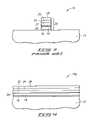
- FIG. 1illustrates a semiconductive wafer fragment 10 at a preliminary step of a prior art gate structure patterning process.
- Semiconductive wafer fragment 10comprises a substrate 12 having a stack 14 of materials formed thereover.
- Substrate 12can comprise, for example, monocrystalline silicon lightly doped with a p-type background dopant.
- the term “semiconductive substrate”is defined to mean any construction comprising semiconductive material, including, but not limited to, bulk semiconductive materials such as a semiconductive wafer (either alone or in assemblies comprising other materials thereon), and semiconductive material layers (either alone or in assemblies comprising other materials).
- substraterefers to any supporting structure, including, but not limited to, the semiconductive substrates described above.
- Stack 14comprises a gate oxide layer 16 , a polysilicon layer 18 , a metal silicide layer 20 , an oxide layer 22 , a nitride layer 24 , an antireflective material layer 26 , and a photoresist layer 28 .
- Gate oxide layer 16can comprise, for example, silicon dioxide, and forms an insulating layer between polysilicon layer 18 and substrate 12 .
- Polysilicon layer 18can comprise, for example, conductively doped polysilicon, and will ultimately be patterned into a first conductive portion of a transistor gate.
- Silicide layer 20comprises a metal silicide, such as, for example, tungsten silicide or titanium silicide, and will ultimately comprise a second conductive portion of a transistor gate.
- a metal silicidesuch as, for example, tungsten silicide or titanium silicide
- the silicidePrior to utilization of silicide layer 20 as a conductive portion of a transistor gate, the silicide is typically subjected to an anneal to improve crystallinity and conductivity of the silicide material of layer 20 .
- Such annealcan comprise, for example, a temperature of from about 800° C. to about 900° C. for a time of about thirty minutes with a nitrogen (N 2 ) purge.
- oxide layer 22is preferably provided over silicide layer 20 prior to the anneal.
- Oxide layer 22can comprise, for example, silicon dioxide.
- Another purpose of having oxide layer 22 over silicide layer 20is as an insulative layer to prevent electrical contact of silicide layer 20 with other conductive layers ultimately formed proximate silicide layer 20 .
- Nitride layer 24can comprise, for example, silicon nitride, and is provided to further electrically insulate conductive layers 18 and 20 from other conductive layers which may ultimately be formed proximate layers 18 and 20 .
- Nitride layer 24is a thick layer (a typical thickness can be on the order of several hundred, or a few thousand Angstroms) and can create stress on underlying layers. Accordingly, another function of oxide layer 22 is to alleviate stress induced by nitride layer 24 on underlying layers 18 and 20 .
- Antireflective material layer 26can comprise, for example, an organic layer that is spun over nitride layer 24 .
- layer 26can be a deposited inorganic antireflective material, such as, for example, Si x O y N z :H, wherein x is from 0.39 to 0.65, y is from 0.02 to 0.56, and z is from 0.05 to 0.33.
- the layercan be substantially inorganic, with the term “substantially inorganic” indicating that the layer can contain a small amount of carbon (less than 1% by weight). Alternatively, if, for example, organic precursors are utilized, the layer can have greater than or equal to 1% carbon, by weight.
- Photoresist layer 28can comprise either a positive or a negative photoresist.
- Photoresist layer 28is patterned by exposing the layer to light through a masked light source.
- the maskcontains clear and opaque features defining a pattern to be created in photoresist layer 28 .
- Regions of photoresist layer 28 which are exposed to lightare made either soluble or insoluble in a solvent. If the exposed regions are soluble, a positive image of the mask is produced in photoresist layer 28 and the resist is termed a positive photoresist.
- the photoresistis referred to as a negative photoresist.
- a difficulty that can occur when exposing photoresist layer 28 to radiationis that waves of the radiation can propagate through photoresist 28 to a layer beneath the photoresist and then be reflected back up through the photoresist to interact with other waves of the radiation which are propagating through the photoresist.
- the reflected wavescan constructively and/or destructively interfere with the other waves to create periodic variations of light intensity within the photoresist.
- Such variations of light intensitycan cause the photoresist to receive non-uniform doses of energy throughout its thickness.
- the non-uniform dosescan decrease the accuracy and precision with which a masked pattern is transferred to the photoresist.
- Antireflective material 26is provided to suppress waves from reflecting back into photoresist layer 28 .
- Antireflective layer 26comprises materials which absorb and/or attenuate radiation and which therefore reduce or eliminate reflection of the radiation.
- FIG. 2shows semiconductive wafer fragment 10 after photoresist layer 28 is patterned by exposure to light and solvent to remove portions of layer 28 .
- a pattern from layer 28is transferred to underlying layers 16 , 18 , 20 , 22 , 24 , and 26 to form a patterned stack 30 .
- Such transfer of a pattern from masking layer 28can occur by a suitable etch, such as, for example, a plasma etch utilizing one or more of Cl, HBr, CF 4 , CH 2 F 2 , He, and NF 3 .
- layers 28 and 26can be removed to leave a patterned gate stack comprising layers 16 , 18 , 20 , 22 , and 24 .
- a continuing goal in semiconductor wafer fabrication technologiesis to reduce process complexity. Such reduction can comprise, for example, reducing a number of process steps, or reducing a number of layers utilized in forming a particular semiconductor structure. Accordingly, it would be desirable to develop alternative methods of forming patterned gate stacks wherein fewer steps and/or layers are utilized than those utilized in the prior art embodiment described with reference to FIGS. 1-3 .
- the inventionencompasses a semiconductor processing method.
- a metal silicide layeris formed over a substrate.
- An antireflective material layeris chemical vapor deposited in physical contact with the metal silicide layer.
- a layer of photoresistis applied over the antireflective material layer and patterned photolithographically.
- the inventionencompasses a gate stack forming method.
- a polysilicon layeris formed over a substrate.
- a metal silicide layeris formed over the polysilicon layer.
- An antireflective material layeris deposited over the metal silicide layer.
- a silicon nitride layeris formed over the antireflective material layer and a layer of photoresist is formed over the silicon nitride layer.
- the layer of photoresistis photolithographically patterned to form a masking layer from the layer of photoresist.
- a patternis transferred from the is masking layer to the silicon nitride layer, antireflective material layer, metal silicide layer and polysilicon layer to pattern the silicon nitride layer, antireflective material layer, metal silicide layer and polysilicon layer into a gate stack.
- the inventionencompasses a gate stack comprising a polysilicon layer over a semiconductive substrate.
- the gate stackfurther comprises a metal silicide layer over the polysilicon layer, and a layer comprising silicon, oxygen and nitrogen over the metal silicide.
- the gate stackcomprises a silicon nitride layer over the layer comprising silicon, oxygen and nitrogen.
- FIG. 1is a fragmentary, diagrammatic, cross-sectional view of a semiconductive wafer fragment at a preliminary processing step of a prior art process.
- FIG. 2is a view of the FIG. 1 wafer fragment at a prior art processing step subsequent to that of FIG. 1 .
- FIG. 3is a view of the FIG. 1 wafer fragment at a prior art processing step subsequent to that of FIG. 2 .
- FIG. 4is a fragmentary, diagrammatic, cross-sectional view of a semiconductive wafer fragment at a preliminary processing step of a method of the present invention.
- FIG. 5is a view of the FIG. 4 wafer fragment at a processing step subsequent to that of FIG. 4 .
- FIG. 6is a view of the FIG. 4 wafer fragment at a processing step subsequent to that of FIG. 5 .
- FIGS. 4-6An embodiment encompassed by the present invention is described with reference to FIGS. 4-6 .
- similar numbering to that utilized above in describing the prior art processing of FIGS. 1-3will be used, with differences indicated by the suffix “a”, or by different numerals.
- Wafer fragment 10 alike the wafer fragment 10 of FIGS. 1-3 , comprises a substrate 12 , a gate oxide layer 16 , a polysilicon layer 18 , and a silicide layer 20 .
- a layer 50comprising silicon, nitrogen, and oxygen is formed over silicide 20 , and in the shown preferred embodiment is formed in physical contact with silicide layer 20 .
- Layer 50thus replaces the oxide layer 22 of the prior art embodiment of FIGS. 1-3 .
- Layer 50is preferably formed by chemical vapor deposition (CVD).
- Layer 50can be formed by, for example, CVD utilizing SiH 4 and N 2 O as precursors, in a reaction chamber at a temperature of about 400° C. Such deposition can be performed either with or without a plasma being present within the reaction chamber.
- CVDchemical vapor deposition
- Exemplary conditions for depositing layer 50include flowing SiH 4 into a plasma-enhanced CVD chamber at a rate of from about 40 standard cubic centimeters per minute (SCCM) to about 300 SCCM (preferably about 80 SCCM), N 2 O at a rate of from about 80 SCCM to about 600 SCCM (preferably about 80 SCCM), He at a rate from about 1300 SCCM to about 2500 SCCM (preferably about 2200 SCCM), with a pressure within the chamber of from about 4 Torr to about 6.5 Torr, and a power to the chamber of from about 50 watts to about 200 watts (preferably about 100 watts).
- SCCMstandard cubic centimeters per minute
- N 2 Oat a rate of from about 80 SCCM to about 600 SCCM (preferably about 80 SCCM)
- Heat a rate from about 1300 SCCM to about 2500 SCCM (preferably about 2200 SCCM)
- a pressure within the chamberof from about 4 Torr to about 6.5 Torr
- a power to the chamberof from about 50
- the above-described exemplary conditionscan further include flowing nitrogen gas (N 2 ) into the reaction chamber at a rate of from greater than 0 SCCM to about 300 SCCM, and preferably at a rate of about 200 SCCM, and/or flowing NH 3 into the reaction chamber at a rate of from greater than 0 SCCM to about 100 SCCM.
- N 2nitrogen gas
- the relative values of x, y, z and the hydrogen contentcan be adjusted to alter absorbance characteristics of the deposited material.
- Layer 50preferably has a thickness of from about 250 ⁇ to about 650 ⁇ .
- Layer 50is preferably provided over silicide layer 20 before annealing layer 20 .
- Layer 50thus provides the above-described function of oxide layer 22 (described with reference to FIGS. 1-3 ) of protecting silicide layer 20 from exposure to gaseous oxygen during annealing of the silicide layer.
- a silicon nitride layer 24is formed over layer 50 , and can be in physical contact with layer 50 .
- silicon nitride layer 24can exert stress on underlying layers.
- layer 50can serve a function of prior art silicon dioxide layer 22 (discussed with reference to FIGS. 1-3 ) of alleviating such stress from adversely impacting underlying conductive layers 20 and 18 .
- Silicon nitride layer 24can be formed over layer 50 either before or after annealing silicide layer 20 .
- a photoresist layer 28is formed over silicon nitride layer 24 .
- layer 50is preferably utilized to serve the function of an antireflective material.
- nitride layer 24is effectively transparent to radiation utilized in patterning photoresist layer 28 . Accordingly, radiation which penetrates photoresist layer 28 will generally also penetrate silicon nitride layer 24 and thereafter enter layer 50 .
- the stoichiometry of silicon, oxygen and nitrogen of layer 50is appropriately adjusted to cancel radiation reaching layer 50 from being reflected back into photoresist layer 28 .
- layers 24 and 50can be tuned in thickness (by adjusting thickness of one or both of layers 24 and 50 ) and stoichiometry (by adjusting a stoichiometry of layer 50 ) such that reflection back into an overlying layer of photoresist is minimized.
- photoresist layer 28is patterned to form a patterned mask over a stack 60 comprising layers 16 , 18 , 20 , 50 and 24 .
- a pattern from photoresist layer 28is transferred to stack 60 ( FIG. 5 ) to form a patterned gate stack 70 comprising layers 16 , 18 , 20 , 50 and 24 .
- Such transfer of a pattern from layer 28can be accomplished by, for example, a plasma etch utilizing one or more of Cl, HBr, CF 4 , CH 2 F 2 , He and NF 3 .
- Photoresist layer 28can then be removed from over gate stack 70 . Subsequently, source and drain regions can be implanted adjacent the gate stack, and sidewall spacers can be provided over sidewalls of the gate stack to complete construction of a transistor gate from gate stack 70 .
- the method of the present inventioncan reduce complexity relative to the prior art gate stack forming method described above with reference to FIGS. 1-3 .
- the method of the present inventioncan utilize a single layer ( 50 ) to accomplish the various functions of protecting silicide during annealing, reducing stress from an overlying silicon nitride layer, and alleviating reflections of light during photolithographic processing of an overlying photoresist layer.
- the method of the present inventioncan eliminate an entire layer (antireflective layer 26 of FIGS. 1-3 ) relative to the prior art process described with reference to FIGS. 1-3 .
- Such elimination of a layeralso eliminates fabrication steps associated with forming and removing the layer. Accordingly, methods encompassed by the present invention can be more efficient semiconductor fabrication processes then prior art methods.
Landscapes
- Engineering & Computer Science (AREA)
- Condensed Matter Physics & Semiconductors (AREA)
- General Physics & Mathematics (AREA)
- Manufacturing & Machinery (AREA)
- Computer Hardware Design (AREA)
- Microelectronics & Electronic Packaging (AREA)
- Power Engineering (AREA)
- Physics & Mathematics (AREA)
- Insulated Gate Type Field-Effect Transistor (AREA)
- Electrodes Of Semiconductors (AREA)
- Internal Circuitry In Semiconductor Integrated Circuit Devices (AREA)
- Formation Of Insulating Films (AREA)
- Exposure Of Semiconductors, Excluding Electron Or Ion Beam Exposure (AREA)
- Semiconductor Memories (AREA)
- Semiconductor Integrated Circuits (AREA)
- Junction Field-Effect Transistors (AREA)
Abstract
Description
Claims (13)
Priority Applications (2)
| Application Number | Priority Date | Filing Date | Title |
|---|---|---|---|
| US09/559,903US7576400B1 (en) | 1998-09-03 | 2000-04-26 | Circuitry and gate stacks |
| US12/537,577US20090294878A1 (en) | 1998-09-03 | 2009-08-07 | Circuitry and gate stacks |
Applications Claiming Priority (2)
| Application Number | Priority Date | Filing Date | Title |
|---|---|---|---|
| US09/146,842US6281100B1 (en) | 1998-09-03 | 1998-09-03 | Semiconductor processing methods |
| US09/559,903US7576400B1 (en) | 1998-09-03 | 2000-04-26 | Circuitry and gate stacks |
Related Parent Applications (1)
| Application Number | Title | Priority Date | Filing Date |
|---|---|---|---|
| US09/146,842DivisionUS6281100B1 (en) | 1998-09-03 | 1998-09-03 | Semiconductor processing methods |
Related Child Applications (1)
| Application Number | Title | Priority Date | Filing Date |
|---|---|---|---|
| US12/537,577ContinuationUS20090294878A1 (en) | 1998-09-03 | 2009-08-07 | Circuitry and gate stacks |
Publications (1)
| Publication Number | Publication Date |
|---|---|
| US7576400B1true US7576400B1 (en) | 2009-08-18 |
Family
ID=22519209
Family Applications (4)
| Application Number | Title | Priority Date | Filing Date |
|---|---|---|---|
| US09/146,842Expired - LifetimeUS6281100B1 (en) | 1998-09-03 | 1998-09-03 | Semiconductor processing methods |
| US09/559,903Expired - Fee RelatedUS7576400B1 (en) | 1998-09-03 | 2000-04-26 | Circuitry and gate stacks |
| US09/870,850Expired - LifetimeUS6461950B2 (en) | 1998-09-03 | 2001-05-30 | Semiconductor processing methods, semiconductor circuitry, and gate stacks |
| US12/537,577AbandonedUS20090294878A1 (en) | 1998-09-03 | 2009-08-07 | Circuitry and gate stacks |
Family Applications Before (1)
| Application Number | Title | Priority Date | Filing Date |
|---|---|---|---|
| US09/146,842Expired - LifetimeUS6281100B1 (en) | 1998-09-03 | 1998-09-03 | Semiconductor processing methods |
Family Applications After (2)
| Application Number | Title | Priority Date | Filing Date |
|---|---|---|---|
| US09/870,850Expired - LifetimeUS6461950B2 (en) | 1998-09-03 | 2001-05-30 | Semiconductor processing methods, semiconductor circuitry, and gate stacks |
| US12/537,577AbandonedUS20090294878A1 (en) | 1998-09-03 | 2009-08-07 | Circuitry and gate stacks |
Country Status (8)
| Country | Link |
|---|---|
| US (4) | US6281100B1 (en) |
| EP (1) | EP1114444B1 (en) |
| JP (1) | JP2003506854A (en) |
| KR (1) | KR100434560B1 (en) |
| AT (1) | ATE345580T1 (en) |
| AU (1) | AU5590699A (en) |
| DE (1) | DE69934019T2 (en) |
| WO (1) | WO2000014780A1 (en) |
Cited By (1)
| Publication number | Priority date | Publication date | Assignee | Title |
|---|---|---|---|---|
| US9748160B2 (en) | 2015-10-16 | 2017-08-29 | Samsung Electronics Co., Ltd. | Semiconductor package, method of fabricating the same, and semiconductor module |
Families Citing this family (26)
| Publication number | Priority date | Publication date | Assignee | Title |
|---|---|---|---|---|
| US6274292B1 (en)* | 1998-02-25 | 2001-08-14 | Micron Technology, Inc. | Semiconductor processing methods |
| US7804115B2 (en) | 1998-02-25 | 2010-09-28 | Micron Technology, Inc. | Semiconductor constructions having antireflective portions |
| US6291868B1 (en)* | 1998-02-26 | 2001-09-18 | Micron Technology, Inc. | Forming a conductive structure in a semiconductor device |
| US6268282B1 (en) | 1998-09-03 | 2001-07-31 | Micron Technology, Inc. | Semiconductor processing methods of forming and utilizing antireflective material layers, and methods of forming transistor gate stacks |
| US6828683B2 (en) | 1998-12-23 | 2004-12-07 | Micron Technology, Inc. | Semiconductor devices, and semiconductor processing methods |
| US7235499B1 (en)* | 1999-01-20 | 2007-06-26 | Micron Technology, Inc. | Semiconductor processing methods |
| US6291361B1 (en)* | 1999-03-24 | 2001-09-18 | Conexant Systems, Inc. | Method and apparatus for high-resolution in-situ plasma etching of inorganic and metal films |
| US7067414B1 (en) | 1999-09-01 | 2006-06-27 | Micron Technology, Inc. | Low k interlevel dielectric layer fabrication methods |
| JP3498022B2 (en)* | 1999-10-15 | 2004-02-16 | Necエレクトロニクス株式会社 | Method for manufacturing semiconductor device |
| US6440860B1 (en) | 2000-01-18 | 2002-08-27 | Micron Technology, Inc. | Semiconductor processing methods of transferring patterns from patterned photoresists to materials, and structures comprising silicon nitride |
| KR100408743B1 (en)* | 2001-09-21 | 2003-12-11 | 삼성전자주식회사 | Method of forming a quantum dot and method of forming a gate electrode using the same |
| US6573175B1 (en)* | 2001-11-30 | 2003-06-03 | Micron Technology, Inc. | Dry low k film application for interlevel dielectric and method of cleaning etched features |
| US6777829B2 (en) | 2002-03-13 | 2004-08-17 | Celis Semiconductor Corporation | Rectifier utilizing a grounded antenna |
| US6720235B2 (en)* | 2002-09-10 | 2004-04-13 | Silicon Integrated System Corp. | Method of forming shallow trench isolation in a semiconductor substrate |
| US7384727B2 (en)* | 2003-06-26 | 2008-06-10 | Micron Technology, Inc. | Semiconductor processing patterning methods |
| US7115532B2 (en) | 2003-09-05 | 2006-10-03 | Micron Technolgoy, Inc. | Methods of forming patterned photoresist layers over semiconductor substrates |
| US7132201B2 (en)* | 2003-09-12 | 2006-11-07 | Micron Technology, Inc. | Transparent amorphous carbon structure in semiconductor devices |
| US7129180B2 (en)* | 2003-09-12 | 2006-10-31 | Micron Technology, Inc. | Masking structure having multiple layers including an amorphous carbon layer |
| US6969677B2 (en)* | 2003-10-20 | 2005-11-29 | Micron Technology, Inc. | Methods of forming conductive metal silicides by reaction of metal with silicon |
| US7026243B2 (en)* | 2003-10-20 | 2006-04-11 | Micron Technology, Inc. | Methods of forming conductive material silicides by reaction of metal with silicon |
| US7153769B2 (en)* | 2004-04-08 | 2006-12-26 | Micron Technology, Inc. | Methods of forming a reaction product and methods of forming a conductive metal silicide by reaction of metal with silicon |
| US7119031B2 (en)* | 2004-06-28 | 2006-10-10 | Micron Technology, Inc. | Methods of forming patterned photoresist layers over semiconductor substrates |
| US7241705B2 (en)* | 2004-09-01 | 2007-07-10 | Micron Technology, Inc. | Methods of forming conductive contacts to source/drain regions and methods of forming local interconnects |
| JP2009071232A (en)* | 2007-09-18 | 2009-04-02 | Elpida Memory Inc | Semiconductor device and manufacturing method thereof |
| CN108172621A (en)* | 2018-01-19 | 2018-06-15 | 矽力杰半导体技术(杭州)有限公司 | LDMOS transistor and its manufacturing method |
| CN112331558B (en)* | 2020-10-23 | 2023-09-15 | 杭州芯迈半导体技术有限公司 | LDMOS transistor and manufacturing method |
Citations (208)
| Publication number | Priority date | Publication date | Assignee | Title |
|---|---|---|---|---|
| US4158717A (en) | 1977-02-14 | 1979-06-19 | Varian Associates, Inc. | Silicon nitride film and method of deposition |
| US4444617A (en) | 1983-01-06 | 1984-04-24 | Rockwell International Corporation | Reactive ion etching of molybdenum silicide and N+ polysilicon |
| US4474975A (en) | 1983-05-09 | 1984-10-02 | The United States Of America As Represented By The Administrator Of The National Aeronautics And Space Administration | Process for producing tris (N-methylamino) methylsilane |
| US4523214A (en) | 1981-07-03 | 1985-06-11 | Fuji Photo Film Co., Ltd. | Solid state image pickup device utilizing microcrystalline and amorphous silicon |
| US4552783A (en)* | 1984-11-05 | 1985-11-12 | General Electric Company | Enhancing the selectivity of tungsten deposition on conductor and semiconductor surfaces |
| US4562091A (en) | 1982-12-23 | 1985-12-31 | International Business Machines Corporation | Use of plasma polymerized orgaosilicon films in fabrication of lift-off masks |
| US4592129A (en) | 1985-04-01 | 1986-06-03 | Motorola, Inc. | Method of making an integral, multiple layer antireflection coating by hydrogen ion implantation |
| US4600671A (en) | 1983-09-12 | 1986-07-15 | Canon Kabushiki Kaisha | Photoconductive member having light receiving layer of A-(Si-Ge) and N |
| US4648904A (en) | 1986-02-14 | 1987-03-10 | Scm Corporation | Aqueous systems containing silanes for rendering masonry surfaces water repellant |
| US4695859A (en) | 1986-10-20 | 1987-09-22 | Energy Conversion Devices, Inc. | Thin film light emitting diode, photonic circuit employing said diode imager employing said circuits |
| US4702936A (en) | 1984-09-20 | 1987-10-27 | Applied Materials Japan, Inc. | Gas-phase growth process |
| US4755478A (en) | 1987-08-13 | 1988-07-05 | International Business Machines Corporation | Method of forming metal-strapped polysilicon gate electrode for FET device |
| US4764247A (en) | 1987-03-18 | 1988-08-16 | Syn Labs, Inc. | Silicon containing resists |
| JPS63157443U (en) | 1987-03-30 | 1988-10-14 | ||
| JPS63316476A (en) | 1987-06-18 | 1988-12-23 | Seiko Instr & Electronics Ltd | Semiconductor device and manufacture thereof |
| US4805683A (en) | 1988-03-04 | 1989-02-21 | International Business Machines Corporation | Method for producing a plurality of layers of metallurgy |
| US4833096A (en) | 1988-01-19 | 1989-05-23 | Atmel Corporation | EEPROM fabrication process |
| US4863755A (en) | 1987-10-16 | 1989-09-05 | The Regents Of The University Of California | Plasma enhanced chemical vapor deposition of thin films of silicon nitride from cyclic organosilicon nitrogen precursors |
| US4870470A (en) | 1987-10-16 | 1989-09-26 | International Business Machines Corporation | Non-volatile memory cell having Si rich silicon nitride charge trapping layer |
| US4905073A (en)* | 1987-06-22 | 1990-02-27 | At&T Bell Laboratories | Integrated circuit with improved tub tie |
| US4907064A (en)* | 1986-09-08 | 1990-03-06 | Nec Corporation | Semiconductor device having silicon oxynitride film with improved moisture resistance |
| US4910160A (en) | 1989-06-06 | 1990-03-20 | National Semiconductor Corporation | High voltage complementary NPN/PNP process |
| US4940509A (en) | 1988-03-25 | 1990-07-10 | Texas Instruments, Incorporated | Isotropic etchant for capped silicide processes |
| US4971655A (en) | 1989-12-26 | 1990-11-20 | Micron Technology, Inc. | Protection of a refractory metal silicide during high-temperature processing using a dual-layer cap of silicon dioxide and silicon nitride |
| US4992306A (en) | 1990-02-01 | 1991-02-12 | Air Products Abd Chemicals, Inc. | Deposition of silicon dioxide and silicon oxynitride films using azidosilane sources |
| US5034348A (en) | 1990-08-16 | 1991-07-23 | International Business Machines Corp. | Process for forming refractory metal silicide layers of different thicknesses in an integrated circuit |
| US5036383A (en) | 1989-04-27 | 1991-07-30 | Kabushiki Kaisha Toshiba | Semiconductor device having an improved bonding pad |
| US5061509A (en) | 1989-08-25 | 1991-10-29 | Kabushiki Kaisha Toshiba | Method of manufacturing polyimide thin film and method of manufacturing liquid crystal orientation film of polyimide |
| EP0464515A3 (en) | 1990-06-28 | 1992-05-06 | Kabushiki Kaisha Toshiba | Method of manufacturing silicon nitride film |
| US5140390A (en) | 1990-02-16 | 1992-08-18 | Hughes Aircraft Company | High speed silicon-on-insulator device |
| US5219613A (en) | 1990-06-13 | 1993-06-15 | Wacker-Chemitronic Gesellschaft Fur Elektronik-Grundstoffe Mbh | Process for producing storage-stable surfaces of polished silicon wafers |
| US5244537A (en) | 1989-12-27 | 1993-09-14 | Honeywell, Inc. | Fabrication of an electronic microvalve apparatus |
| JPH05263255A (en) | 1992-03-19 | 1993-10-12 | Hitachi Electron Eng Co Ltd | Plasma cvd device |
| US5260600A (en) | 1990-06-05 | 1993-11-09 | Mitsubishi Denki Kabushiki Kaisha | Semiconductor device having protective insulating film |
| US5270267A (en) | 1989-05-31 | 1993-12-14 | Mitel Corporation | Curing and passivation of spin on glasses by a plasma process wherein an external polarization field is applied to the substrate |
| US5286661A (en) | 1992-08-26 | 1994-02-15 | Motorola, Inc. | Method of forming a bipolar transistor having an emitter overhang |
| JPH0667019A (en) | 1992-01-17 | 1994-03-11 | Asahi Glass Co Ltd | Antireflection layer and its production |
| EP0588087A2 (en) | 1992-08-20 | 1994-03-23 | Sony Corporation | Method of determining optimum optical conditions for an anti-reflective layer used in a method of forming a resist pattern |
| US5302366A (en) | 1991-03-28 | 1994-04-12 | Phillips Petroleum Company | Production of silicon product containing both carbon and nitrogen |
| US5312768A (en) | 1993-03-09 | 1994-05-17 | Micron Technology, Inc. | Integrated process for fabricating raised, source/drain, short-channel transistors |
| US5314724A (en) | 1991-01-08 | 1994-05-24 | Fujitsu Limited | Process for forming silicon oxide film |
| US5340621A (en) | 1992-03-30 | 1994-08-23 | Nippon Sheet Glass Co., Ltd. | Plasma CVD method |
| JPH06244172A (en) | 1993-02-18 | 1994-09-02 | Toray Ind Inc | Multilayered wiring structure |
| US5356515A (en) | 1990-10-19 | 1994-10-18 | Tokyo Electron Limited | Dry etching method |
| US5376591A (en) | 1992-06-05 | 1994-12-27 | Semiconductor Process Laboratory Co., Ltd. | Method for manufacturing semiconductor device |
| US5405489A (en) | 1991-10-30 | 1995-04-11 | Samsung Electronics Co., Ltd. | Method for fabricating an interlayer-dielectric film of a semiconductor device by using a plasma treatment prior to reflow |
| US5413963A (en) | 1994-08-12 | 1995-05-09 | United Microelectronics Corporation | Method for depositing an insulating interlayer in a semiconductor metallurgy system |
| US5429987A (en) | 1993-01-25 | 1995-07-04 | Sharp Microelectronics Technology, Inc. | Method for profile control of selective metallization |
| JPH07201716A (en) | 1993-12-29 | 1995-08-04 | Sony Corp | Semiconductor device and its manufacture |
| US5439838A (en) | 1994-09-14 | 1995-08-08 | United Microelectronics Corporation | Method of thinning for EEPROM tunneling oxide device |
| US5441797A (en) | 1993-04-27 | 1995-08-15 | International Business Machines Corporation | Antireflective polyimide dielectric for photolithography |
| US5461003A (en) | 1994-05-27 | 1995-10-24 | Texas Instruments Incorporated | Multilevel interconnect structure with air gaps formed between metal leads |
| US5470772A (en) | 1991-11-06 | 1995-11-28 | Intel Corporation | Silicidation method for contactless EPROM related devices |
| US5472829A (en) | 1991-12-30 | 1995-12-05 | Sony Corporation | Method of forming a resist pattern by using an anti-reflective layer |
| US5472827A (en) | 1991-12-30 | 1995-12-05 | Sony Corporation | Method of forming a resist pattern using an anti-reflective layer |
| US5482894A (en)* | 1994-08-23 | 1996-01-09 | Texas Instruments Incorporated | Method of fabricating a self-aligned contact using organic dielectric materials |
| JPH0845926A (en) | 1994-07-26 | 1996-02-16 | Sony Corp | Semiconductor device and its manufacture |
| JPH0846186A (en) | 1994-07-27 | 1996-02-16 | Sony Corp | Semiconductor device |
| US5498555A (en) | 1994-11-07 | 1996-03-12 | United Microelectronics Corporation | Method of making LDD with polysilicon and dielectric spacers |
| US5536857A (en) | 1994-07-05 | 1996-07-16 | Ford Motor Company | Single source volatile precursor for SiO2.TiO2 powders and films |
| US5541445A (en) | 1991-08-14 | 1996-07-30 | Mitel Corporation | High performance passivation for semiconductor devices |
| US5543654A (en) | 1992-01-28 | 1996-08-06 | Thunderbird Technologies, Inc. | Contoured-tub fermi-threshold field effect transistor and method of forming same |
| JPH08213386A (en) | 1995-02-08 | 1996-08-20 | Fujitsu Ltd | Method for manufacturing semiconductor device |
| US5554567A (en) | 1994-09-01 | 1996-09-10 | Taiwan Semiconductor Manufacturing Company Ltd. | Method for improving adhesion to a spin-on-glass |
| US5591494A (en) | 1993-09-24 | 1997-01-07 | Applied Materials, Inc. | Deposition of silicon nitrides by plasma-enhanced chemical vapor deposition |
| US5593741A (en) | 1992-11-30 | 1997-01-14 | Nec Corporation | Method and apparatus for forming silicon oxide film by chemical vapor deposition |
| US5600165A (en) | 1994-07-27 | 1997-02-04 | Sony Corporation | Semiconductor device with antireflection film |
| JPH0950993A (en) | 1995-08-08 | 1997-02-18 | Fujitsu Ltd | Insulating film forming method and semiconductor device |
| US5605601A (en) | 1995-09-19 | 1997-02-25 | Mitsubishi Denki Kabushiki Kaisha | Method of manufacturing semiconductor device |
| JPH0955351A (en) | 1995-08-15 | 1997-02-25 | Sony Corp | Manufacture of semiconductor device |
| EP0771886A1 (en) | 1995-10-30 | 1997-05-07 | Dow Corning Corporation | Method for depositing amorphous SiNC coatings |
| EP0778496A2 (en) | 1995-12-05 | 1997-06-11 | Applied Materials, Inc. | Method and apparatus for depositing antireflective coating |
| US5639689A (en) | 1993-12-29 | 1997-06-17 | Hyundai Electronics Industries Co., Ltd. | Method for fabricating storage electrode of semiconductor device |
| US5639687A (en) | 1993-07-06 | 1997-06-17 | Motorola Inc. | Method for forming an integrated circuit pattern on a semiconductor substrate using silicon-rich silicon nitride |
| US5652187A (en) | 1991-10-30 | 1997-07-29 | Samsung Electronics Co., Ltd. | Method for fabricating doped interlayer-dielectric film of semiconductor device using a plasma treatment |
| US5653619A (en) | 1992-03-02 | 1997-08-05 | Micron Technology, Inc. | Method to form self-aligned gate structures and focus rings |
| US5656330A (en) | 1994-03-22 | 1997-08-12 | Futaba Denshi Kogyo K.K. | Resistive element having a resistivity which is thermally stable against heat treatment, and method and apparatus for producing same |
| US5656337A (en) | 1993-08-31 | 1997-08-12 | Samsung Electronics Co., Ltd. | Method of forming a dielectric layer |
| US5661093A (en) | 1996-09-12 | 1997-08-26 | Applied Materials, Inc. | Method for the stabilization of halogen-doped films through the use of multiple sealing layers |
| US5667015A (en) | 1995-02-03 | 1997-09-16 | Bj Services Company | Well barrier |
| US5670297A (en) | 1991-12-30 | 1997-09-23 | Sony Corporation | Process for the formation of a metal pattern |
| US5674356A (en) | 1994-04-05 | 1997-10-07 | Sony Corporation | Method for forming a semiconductor device in which an anti reflective layer is formed by varying the composition thereof |
| US5677015A (en) | 1994-03-17 | 1997-10-14 | Sony Corporation | High dielectric constant material containing tantalum, process for forming high dielectric constant film containing tantalum, and semiconductor device using the same |
| US5677111A (en) | 1991-12-20 | 1997-10-14 | Sony Corporation | Process for production of micropattern utilizing antireflection film |
| US5691212A (en) | 1996-09-27 | 1997-11-25 | Taiwan Semiconductor Manufacturing Company, Ltd. | MOS device structure and integration method |
| US5710067A (en) | 1995-06-07 | 1998-01-20 | Advanced Micro Devices, Inc. | Silicon oxime film |
| US5709741A (en) | 1995-02-28 | 1998-01-20 | Dow Corning Toray Silicone Co., Ltd. | Water repellent for application to glass and water-repellent glass |
| US5711987A (en) | 1996-10-04 | 1998-01-27 | Dow Corning Corporation | Electronic coatings |
| US5731242A (en) | 1993-10-15 | 1998-03-24 | Intel Corporation | Self-aligned contact process in semiconductor fabrication |
| US5741721A (en) | 1994-02-01 | 1998-04-21 | Quality Microcircuits Corporation | Method of forming capacitors and interconnect lines |
| US5744399A (en) | 1995-11-13 | 1998-04-28 | Lsi Logic Corporation | Process for forming low dielectric constant layers using fullerenes |
| US5747388A (en) | 1992-09-18 | 1998-05-05 | Siemens Aktiengesellschaft | Antireflection layer and process for lithographically structuring a layer |
| US5750442A (en) | 1995-09-25 | 1998-05-12 | Micron Technology, Inc. | Germanium as an antireflective coating and method of use |
| US5753320A (en) | 1985-09-26 | 1998-05-19 | Canon Kabushiki Kaisha | Process for forming deposited film |
| US5759755A (en) | 1993-08-08 | 1998-06-02 | Samsung Electronics, Co., Ltd. | Semiconductor substrate containing anti-reflective layer |
| JPH10163083A (en) | 1996-10-15 | 1998-06-19 | Texas Instr Inc <Ti> | Semiconductor treatment method |
| US5780891A (en) | 1994-12-05 | 1998-07-14 | Micron Technology, Inc. | Nonvolatile floating gate memory with improved interploy dielectric |
| US5783493A (en) | 1997-01-27 | 1998-07-21 | Taiwan Semiconductor Manufacturing Company Ltd. | Method for reducing precipitate defects using a plasma treatment post BPSG etchback |
| US5786039A (en) | 1995-05-15 | 1998-07-28 | France Telecom | Process for electrical insulation in microelectronics, applicable in narrow cavities, by deposition of oxide in the viscous state and corresponding device |
| US5792689A (en) | 1997-04-11 | 1998-08-11 | Vanguard International Semiconducter Corporation | Method for manufacturing double-crown capacitors self-aligned to node contacts on dynamic random access memory |
| US5800877A (en) | 1995-08-18 | 1998-09-01 | Canon Sales Co., Inc. | Method for forming a fluorine containing silicon oxide film |
| US5801399A (en)* | 1994-10-13 | 1998-09-01 | Yamaha Corporation | Semiconductor device with antireflection film |
| US5807660A (en) | 1997-02-03 | 1998-09-15 | Taiwan Semiconductor Manufacturing Company Ltd. | Avoid photoresist lifting by post-oxide-dep plasma treatment |
| US5817549A (en) | 1994-08-31 | 1998-10-06 | Semiconductor Energy Laboratory Co., Ltd. | Method for manufacturing a semiconductor device |
| US5838052A (en) | 1996-03-07 | 1998-11-17 | Micron Technology, Inc. | Reducing reflectivity on a semiconductor wafer by annealing titanium and aluminum |
| US5840610A (en) | 1997-01-16 | 1998-11-24 | Advanced Micro Devices, Inc. | Enhanced oxynitride gate dielectrics using NF3 gas |
| US5858880A (en) | 1994-05-14 | 1999-01-12 | Trikon Equipment Limited | Method of treating a semi-conductor wafer |
| US5872035A (en) | 1996-06-29 | 1999-02-16 | Hyundai Electronics Industries Co., Ltd. | Method of forming a floating gate in a flash memory device |
| US5872385A (en) | 1994-05-02 | 1999-02-16 | Motorola Inc. | Conductive interconnect structure and method of formation |
| US5874367A (en) | 1992-07-04 | 1999-02-23 | Trikon Technologies Limited | Method of treating a semi-conductor wafer |
| US5883011A (en) | 1997-06-18 | 1999-03-16 | Vlsi Technology, Inc. | Method of removing an inorganic antireflective coating from a semiconductor substrate |
| US5883014A (en) | 1997-06-03 | 1999-03-16 | United Microelectronics Corp. | Method for treating via sidewalls with hydrogen plasma |
| WO1999020029A1 (en) | 1997-10-14 | 1999-04-22 | Sagem S.A. | Mobile telephone sending audio messages |
| WO1999020030A1 (en) | 1997-10-14 | 1999-04-22 | Ameritech Corporation | Method of sharing and transferring information between isdn telephones |
| US5924000A (en) | 1997-09-19 | 1999-07-13 | Vanguard International Semiconductor Corporation | Method for forming residue free patterned polysilicon layer containing integrated circuit structures |
| US5933721A (en) | 1997-04-21 | 1999-08-03 | Advanced Micro Devices, Inc. | Method for fabricating differential threshold voltage transistor pair |
| US5948482A (en) | 1995-09-19 | 1999-09-07 | University Of New Mexico | Ambient pressure process for preparing aerogel thin films reliquified sols useful in preparing aerogel thin films |
| EP0942330A1 (en) | 1998-03-11 | 1999-09-15 | Applied Materials, Inc. | Process for depositing and developing a plasma polymerized organosilicon photoresist film |
| US5956605A (en) | 1996-09-20 | 1999-09-21 | Micron Technology, Inc. | Use of nitrides for flip-chip encapsulation |
| US5960289A (en) | 1998-06-22 | 1999-09-28 | Motorola, Inc. | Method for making a dual-thickness gate oxide layer using a nitride/oxide composite region |
| US5962581A (en) | 1995-04-28 | 1999-10-05 | Kabushiki Kaisha Toshiba | Silicone polymer composition, method of forming a pattern and method of forming an insulating film |
| US5968611A (en) | 1997-11-26 | 1999-10-19 | The Research Foundation Of State University Of New York | Silicon nitrogen-based films and method of making the same |
| US5981368A (en) | 1998-11-05 | 1999-11-09 | Advanced Micro Devices | Enhanced shallow junction design by polysilicon line width reduction using oxidation with integrated spacer formation |
| US5985519A (en) | 1997-03-19 | 1999-11-16 | Fujitsu Limited | Method of manufacturing semiconductor device using top antireflection film |
| US5986318A (en) | 1996-10-24 | 1999-11-16 | Samsung Electronics Co., Ltd. | (Ge,Si) Nx anti-reflective compositions and integrated circuit devices comprising the same |
| US5994217A (en) | 1996-12-16 | 1999-11-30 | Chartered Semiconductor Manufacturing Ltd. | Post metallization stress relief annealing heat treatment for ARC TiN over aluminum layers |
| US5994730A (en)* | 1996-11-21 | 1999-11-30 | Alliance Semiconductor Corporation | DRAM cell having storage capacitor contact self-aligned to bit lines and word lines |
| US6001747A (en) | 1998-07-22 | 1999-12-14 | Vlsi Technology, Inc. | Process to improve adhesion of cap layers in integrated circuits |
| US6001741A (en) | 1998-04-15 | 1999-12-14 | Lucent Technologies Inc. | Method for making field effect devices and capacitors with improved thin film dielectrics and resulting devices |
| US6004850A (en) | 1998-02-23 | 1999-12-21 | Motorola Inc. | Tantalum oxide anti-reflective coating (ARC) integrated with a metallic transistor gate electrode and method of formation |
| US6008124A (en) | 1996-02-22 | 1999-12-28 | Matsushita Electric Industrial Co., Ltd. | Semiconductor device having improved lamination-structure reliability for buried layers, silicide films and metal films, and a method for forming the same |
| US6008121A (en) | 1996-03-19 | 1999-12-28 | Siemens Aktiengesellschaft | Etching high aspect contact holes in solid state devices |
| US6017779A (en) | 1994-06-15 | 2000-01-25 | Seiko Epson Corporation | Fabrication method for a thin film semiconductor device, the thin film semiconductor device itself, liquid crystal display, and electronic device |
| US6020243A (en) | 1997-07-24 | 2000-02-01 | Texas Instruments Incorporated | Zirconium and/or hafnium silicon-oxynitride gate dielectric |
| US6022404A (en) | 1995-01-12 | 2000-02-08 | Degussa Aktiengesellschaft | Surface-modified, pyrogenically produced mixed oxides, method of their production and use |
| US6028015A (en) | 1999-03-29 | 2000-02-22 | Lsi Logic Corporation | Process for treating damaged surfaces of low dielectric constant organo silicon oxide insulation material to inhibit moisture absorption |
| US6030901A (en) | 1999-06-24 | 2000-02-29 | Advanced Micro Devices, Inc. | Photoresist stripping without degrading low dielectric constant materials |
| JP2000068261A (en) | 1998-08-19 | 2000-03-03 | Toshiba Corp | Method for manufacturing semiconductor device |
| US6040619A (en)* | 1995-06-07 | 2000-03-21 | Advanced Micro Devices | Semiconductor device including antireflective etch stop layer |
| US6054379A (en) | 1998-02-11 | 2000-04-25 | Applied Materials, Inc. | Method of depositing a low k dielectric with organo silane |
| US6057217A (en) | 1996-07-25 | 2000-05-02 | Nec Corporation | Process for production of semiconductor device with foreign element introduced into silicon dioxide film |
| US6060766A (en)* | 1997-08-25 | 2000-05-09 | Advanced Micro Devices, Inc. | Protection of hydrogen sensitive regions in semiconductor devices from the positive charge associated with plasma deposited barriers or layers |
| US6060765A (en)* | 1998-01-05 | 2000-05-09 | Mitsubishi Denki Kabushiki Kaisha | Semiconductor device and a method of manufacturing the same |
| US6071799A (en) | 1997-06-30 | 2000-06-06 | Hyundai Electronics Industries Co., Ltd. | Method of forming a contact of a semiconductor device |
| US6087267A (en) | 1986-03-04 | 2000-07-11 | Motorola, Inc. | Process for forming an integrated circuit |
| US6087064A (en) | 1998-09-03 | 2000-07-11 | International Business Machines Corporation | Silsesquioxane polymers, method of synthesis, photoresist composition, and multilayer lithographic method |
| US6096656A (en) | 1999-06-24 | 2000-08-01 | Sandia Corporation | Formation of microchannels from low-temperature plasma-deposited silicon oxynitride |
| US6121133A (en) | 1997-08-22 | 2000-09-19 | Micron Technology, Inc. | Isolation using an antireflective coating |
| US6124641A (en) | 1997-06-26 | 2000-09-26 | Mitsubishi Denki Kabushiki Kaisha | Semiconductor device organic insulator film |
| US6130168A (en) | 1999-07-08 | 2000-10-10 | Taiwan Semiconductor Manufacturing Company | Using ONO as hard mask to reduce STI oxide loss on low voltage device in flash or EPROM process |
| US6133096A (en) | 1998-12-10 | 2000-10-17 | Su; Hung-Der | Process for simultaneously fabricating a stack gate flash memory cell and salicided periphereral devices |
| US6133618A (en) | 1997-08-14 | 2000-10-17 | Lucent Technologies Inc. | Semiconductor device having an anti-reflective layer and a method of manufacture thereof |
| US6133613A (en)* | 1998-02-03 | 2000-10-17 | Vanguard International Semiconductor Corporation | Anti-reflection oxynitride film for tungsten-silicide substrates |
| US6136636A (en) | 1998-03-25 | 2000-10-24 | Texas Instruments - Acer Incorporated | Method of manufacturing deep sub-micron CMOS transistors |
| US6140151A (en) | 1998-05-22 | 2000-10-31 | Micron Technology, Inc. | Semiconductor wafer processing method |
| US6140677A (en) | 1998-06-26 | 2000-10-31 | Advanced Micro Devices, Inc. | Semiconductor topography for a high speed MOSFET having an ultra narrow gate |
| US6144083A (en) | 1998-06-10 | 2000-11-07 | Micron Technology, Inc. | Method of reducing defects in anti-reflective coatings and semiconductor structures fabricated thereby |
| US6143670A (en) | 1998-12-28 | 2000-11-07 | Taiwan Semiconductor Manufacturing Company | Method to improve adhesion between low dielectric constant layer and silicon containing dielectric layer |
| US6153504A (en) | 1999-08-16 | 2000-11-28 | Advanced Micro Devices, Inc. | Method of using a silicon oxynitride ARC for final metal layer |
| US6156674A (en) | 1998-11-25 | 2000-12-05 | Micron Technology, Inc. | Semiconductor processing methods of forming insulative materials |
| US6159871A (en) | 1998-05-29 | 2000-12-12 | Dow Corning Corporation | Method for producing hydrogenated silicon oxycarbide films having low dielectric constant |
| US6159804A (en) | 1998-09-02 | 2000-12-12 | Advanced Micro Devices, Inc. | Disposable sidewall oxidation fabrication method for making a transistor having an ultra short channel length |
| US6184151B1 (en) | 1997-08-21 | 2001-02-06 | International Business Machines Corporation | Method for forming cornered images on a substrate and photomask formed thereby |
| US6184158B1 (en) | 1996-12-23 | 2001-02-06 | Lam Research Corporation | Inductively coupled plasma CVD |
| US6187657B1 (en) | 1999-03-24 | 2001-02-13 | Advanced Micro Devices, Inc. | Dual material gate MOSFET technique |
| US6187694B1 (en) | 1997-11-10 | 2001-02-13 | Intel Corporation | Method of fabricating a feature in an integrated circuit using two edge definition layers and a spacer |
| US6198144B1 (en) | 1999-08-18 | 2001-03-06 | Micron Technology, Inc. | Passivation of sidewalls of a word line stack |
| US6200835B1 (en) | 1994-10-07 | 2001-03-13 | Micron Technology, Inc. | Methods of forming conductive polysilicon lines and bottom gated thin film transistors, and conductive polysilicon lines and thin film transistors |
| US6204168B1 (en) | 1998-02-02 | 2001-03-20 | Applied Materials, Inc. | Damascene structure fabricated using a layer of silicon-based photoresist material |
| US6207587B1 (en) | 1997-06-24 | 2001-03-27 | Micron Technology, Inc. | Method for forming a dielectric |
| US6209484B1 (en) | 1996-06-28 | 2001-04-03 | Applied Materials, Inc. | Method and apparatus for depositing an etch stop layer |
| US6218292B1 (en) | 1997-12-18 | 2001-04-17 | Advanced Micro Devices, Inc. | Dual layer bottom anti-reflective coating |
| US6225217B1 (en) | 1997-06-27 | 2001-05-01 | Nec Corporation | Method of manufacturing semiconductor device having multilayer wiring |
| US6235568B1 (en) | 1999-01-22 | 2001-05-22 | Intel Corporation | Semiconductor device having deposited silicon regions and a method of fabrication |
| US6235591B1 (en) | 1999-10-25 | 2001-05-22 | Chartered Semiconductor Manufacturing Company | Method to form gate oxides of different thicknesses on a silicon substrate |
| US6238976B1 (en) | 1997-07-08 | 2001-05-29 | Micron Technology, Inc. | Method for forming high density flash memory |
| US20010003064A1 (en) | 1999-12-02 | 2001-06-07 | Nec Corporation | Method for fabricating semiconductor device and apparatus for fabricating same |
| US6268282B1 (en) | 1998-09-03 | 2001-07-31 | Micron Technology, Inc. | Semiconductor processing methods of forming and utilizing antireflective material layers, and methods of forming transistor gate stacks |
| US6284677B1 (en) | 1997-04-18 | 2001-09-04 | United Semiconductor Corp. | Method of forming fluorosilicate glass (FSG) layers with moisture-resistant capability |
| US20010019868A1 (en) | 1999-07-23 | 2001-09-06 | Fernando Gonzalez | Field effect transistor assemblies, integrated circuitry, and methods of forming field effect transistors and integrated circuitry |
| US20010023051A1 (en) | 1995-12-04 | 2001-09-20 | Rolfson J. Brett | Semiconductor processing method of promoting photoresist adhesion to an outer substrate layer predominately comprising silicon nitride |
| US20010038919A1 (en) | 2000-03-20 | 2001-11-08 | Berry Ivan L. | Plasma curing process for porous silica thin film |
| EP1172845A2 (en) | 2000-07-14 | 2002-01-16 | Applied Materials, Inc. | Method for treating dielectric layers with low dielectric constant to reduce oxygen diffusion |
| US20020033486A1 (en) | 2000-08-04 | 2002-03-21 | Samsung Electronics Co., Ltd. | Method for forming an interconnection line using a hydrosilsesquioxane (HSQ) layer as an interlayer insulating layer |
| US6373114B1 (en) | 1998-10-23 | 2002-04-16 | Micron Technology, Inc. | Barrier in gate stack for improved gate dielectric integrity |
| US6403464B1 (en) | 1999-11-03 | 2002-06-11 | Taiwan Semiconductor Manufacturing Company | Method to reduce the moisture content in an organic low dielectric constant material |
| US20020081834A1 (en) | 2000-12-26 | 2002-06-27 | Honeywell International Inc. | Method for eliminating reaction between photoresist and OSG |
| US6429115B1 (en) | 2001-02-27 | 2002-08-06 | United Microelectronics Corp. | Method of manufacturing multilevel interconnects including performing a surface treatment to form a hydrophilic surface layer |
| US6436808B1 (en) | 2000-12-07 | 2002-08-20 | Advanced Micro Devices, Inc. | NH3/N2-plasma treatment to prevent organic ILD degradation |
| US6435943B1 (en) | 2000-10-26 | 2002-08-20 | United Microelectronics Corp. | Method of chemical mechanical polishing organic silicon material with low dielectric constant |
| US6440860B1 (en) | 2000-01-18 | 2002-08-27 | Micron Technology, Inc. | Semiconductor processing methods of transferring patterns from patterned photoresists to materials, and structures comprising silicon nitride |
| US6444593B1 (en) | 1998-12-02 | 2002-09-03 | Advanced Micro Devices, Inc. | Surface treatment of low-K SiOF to prevent metal interaction |
| US6465372B1 (en) | 1999-08-17 | 2002-10-15 | Applied Materials, Inc. | Surface treatment of C-doped SiO2 film to enhance film stability during O2 ashing |
| US6486061B1 (en) | 1999-08-17 | 2002-11-26 | Applied Materials, Inc. | Post-deposition treatment to enhance properties of Si-O-C low K films |
| US6486057B1 (en) | 2001-04-12 | 2002-11-26 | National Science Council | Process for preparing Cu damascene interconnection |
| US6492688B1 (en) | 1999-03-02 | 2002-12-10 | Siemens Aktiengesellschaft | Dual work function CMOS device |
| US6498084B2 (en) | 2001-05-14 | 2002-12-24 | Maxim Integrated Products, Inc. | Method of forming high density EEPROM cell |
| US6503818B1 (en) | 1999-04-02 | 2003-01-07 | Taiwan Semiconductor Manufacturing Company | Delamination resistant multi-layer composite dielectric layer employing low dielectric constant dielectric material |
| US20030013311A1 (en) | 2001-07-03 | 2003-01-16 | Ting-Chang Chang | Method of avoiding dielectric layer deterioation with a low dielectric constant during a stripping process |
| US6518122B1 (en) | 1999-12-17 | 2003-02-11 | Chartered Semiconductor Manufacturing Ltd. | Low voltage programmable and erasable flash EEPROM |
| US6541164B1 (en)* | 1997-10-22 | 2003-04-01 | Applied Materials, Inc. | Method for etching an anti-reflective coating |
| US20030077916A1 (en) | 2001-10-11 | 2003-04-24 | Applied Materials, Inc. | Method of eliminating photoresist poisoning in damascene applications |
| US6627535B2 (en) | 2000-01-19 | 2003-09-30 | Trikon Holdings Ltd. | Methods and apparatus for forming a film on a substrate |
| US6638875B2 (en) | 1999-08-05 | 2003-10-28 | Axcelis Technologies, Inc. | Oxygen free plasma stripping process |
| US20030207594A1 (en) | 2001-06-19 | 2003-11-06 | Catabay Wilbur G. | Plasma treatment of low dielectric constant dielectric material to form structures useful in formation of metal interconnects and/or filled vias for intergrated circuit structure |
| US6720247B2 (en) | 2000-12-14 | 2004-04-13 | Texas Instruments Incorporated | Pre-pattern surface modification for low-k dielectrics using A H2 plasma |
| US20040071878A1 (en) | 2002-08-15 | 2004-04-15 | Interuniversitair Microelektronica Centrum (Imec Vzw) | Surface preparation using plasma for ALD Films |
| US6723631B2 (en) | 2000-09-29 | 2004-04-20 | Renesas Technology Corporation | Fabrication method of semiconductor integrated circuit device |
Family Cites Families (2)
| Publication number | Priority date | Publication date | Assignee | Title |
|---|---|---|---|---|
| US2553314A (en) | 1944-07-01 | 1951-05-15 | Gen Electric | Method of rendering materials water repellent |
| US6436746B1 (en)* | 1998-01-12 | 2002-08-20 | Texas Instruments Incorporated | Transistor having an improved gate structure and method of construction |
- 1998
- 1998-09-03USUS09/146,842patent/US6281100B1/ennot_activeExpired - Lifetime
- 1999
- 1999-08-31JPJP2000569430Apatent/JP2003506854A/enactivePending
- 1999-08-31ATAT99942555Tpatent/ATE345580T1/ennot_activeIP Right Cessation
- 1999-08-31WOPCT/US1999/020029patent/WO2000014780A1/enactiveIP Right Grant
- 1999-08-31DEDE69934019Tpatent/DE69934019T2/ennot_activeExpired - Lifetime
- 1999-08-31EPEP99942555Apatent/EP1114444B1/ennot_activeExpired - Lifetime
- 1999-08-31AUAU55906/99Apatent/AU5590699A/ennot_activeAbandoned
- 1999-08-31KRKR10-2001-7002811Apatent/KR100434560B1/ennot_activeExpired - Fee Related
- 2000
- 2000-04-26USUS09/559,903patent/US7576400B1/ennot_activeExpired - Fee Related
- 2001
- 2001-05-30USUS09/870,850patent/US6461950B2/ennot_activeExpired - Lifetime
- 2009
- 2009-08-07USUS12/537,577patent/US20090294878A1/ennot_activeAbandoned
Patent Citations (224)
| Publication number | Priority date | Publication date | Assignee | Title |
|---|---|---|---|---|
| US4158717A (en) | 1977-02-14 | 1979-06-19 | Varian Associates, Inc. | Silicon nitride film and method of deposition |
| US4523214A (en) | 1981-07-03 | 1985-06-11 | Fuji Photo Film Co., Ltd. | Solid state image pickup device utilizing microcrystalline and amorphous silicon |
| US4562091A (en) | 1982-12-23 | 1985-12-31 | International Business Machines Corporation | Use of plasma polymerized orgaosilicon films in fabrication of lift-off masks |
| US4444617A (en) | 1983-01-06 | 1984-04-24 | Rockwell International Corporation | Reactive ion etching of molybdenum silicide and N+ polysilicon |
| US4474975A (en) | 1983-05-09 | 1984-10-02 | The United States Of America As Represented By The Administrator Of The National Aeronautics And Space Administration | Process for producing tris (N-methylamino) methylsilane |
| US4600671A (en) | 1983-09-12 | 1986-07-15 | Canon Kabushiki Kaisha | Photoconductive member having light receiving layer of A-(Si-Ge) and N |
| US4702936A (en) | 1984-09-20 | 1987-10-27 | Applied Materials Japan, Inc. | Gas-phase growth process |
| US4552783A (en)* | 1984-11-05 | 1985-11-12 | General Electric Company | Enhancing the selectivity of tungsten deposition on conductor and semiconductor surfaces |
| US4592129A (en) | 1985-04-01 | 1986-06-03 | Motorola, Inc. | Method of making an integral, multiple layer antireflection coating by hydrogen ion implantation |
| US5753320A (en) | 1985-09-26 | 1998-05-19 | Canon Kabushiki Kaisha | Process for forming deposited film |
| US4648904A (en) | 1986-02-14 | 1987-03-10 | Scm Corporation | Aqueous systems containing silanes for rendering masonry surfaces water repellant |
| US4648904B1 (en) | 1986-02-14 | 1988-12-06 | ||
| US6087267A (en) | 1986-03-04 | 2000-07-11 | Motorola, Inc. | Process for forming an integrated circuit |
| US4907064A (en)* | 1986-09-08 | 1990-03-06 | Nec Corporation | Semiconductor device having silicon oxynitride film with improved moisture resistance |
| US4695859A (en) | 1986-10-20 | 1987-09-22 | Energy Conversion Devices, Inc. | Thin film light emitting diode, photonic circuit employing said diode imager employing said circuits |
| US4764247A (en) | 1987-03-18 | 1988-08-16 | Syn Labs, Inc. | Silicon containing resists |
| JPS63157443U (en) | 1987-03-30 | 1988-10-14 | ||
| US4954867A (en) | 1987-06-18 | 1990-09-04 | Seiko Instruments Inc. | Semiconductor device with silicon oxynitride over refractory metal gate electrode in LDD structure |
| JPS63316476A (en) | 1987-06-18 | 1988-12-23 | Seiko Instr & Electronics Ltd | Semiconductor device and manufacture thereof |
| US4905073A (en)* | 1987-06-22 | 1990-02-27 | At&T Bell Laboratories | Integrated circuit with improved tub tie |
| US4755478A (en) | 1987-08-13 | 1988-07-05 | International Business Machines Corporation | Method of forming metal-strapped polysilicon gate electrode for FET device |
| US4863755A (en) | 1987-10-16 | 1989-09-05 | The Regents Of The University Of California | Plasma enhanced chemical vapor deposition of thin films of silicon nitride from cyclic organosilicon nitrogen precursors |
| US4870470A (en) | 1987-10-16 | 1989-09-26 | International Business Machines Corporation | Non-volatile memory cell having Si rich silicon nitride charge trapping layer |
| US4833096A (en) | 1988-01-19 | 1989-05-23 | Atmel Corporation | EEPROM fabrication process |
| US4805683A (en) | 1988-03-04 | 1989-02-21 | International Business Machines Corporation | Method for producing a plurality of layers of metallurgy |
| US4940509A (en) | 1988-03-25 | 1990-07-10 | Texas Instruments, Incorporated | Isotropic etchant for capped silicide processes |
| US5036383A (en) | 1989-04-27 | 1991-07-30 | Kabushiki Kaisha Toshiba | Semiconductor device having an improved bonding pad |
| US5270267A (en) | 1989-05-31 | 1993-12-14 | Mitel Corporation | Curing and passivation of spin on glasses by a plasma process wherein an external polarization field is applied to the substrate |
| US4910160A (en) | 1989-06-06 | 1990-03-20 | National Semiconductor Corporation | High voltage complementary NPN/PNP process |
| US5061509A (en) | 1989-08-25 | 1991-10-29 | Kabushiki Kaisha Toshiba | Method of manufacturing polyimide thin film and method of manufacturing liquid crystal orientation film of polyimide |
| US4971655A (en) | 1989-12-26 | 1990-11-20 | Micron Technology, Inc. | Protection of a refractory metal silicide during high-temperature processing using a dual-layer cap of silicon dioxide and silicon nitride |
| US5244537A (en) | 1989-12-27 | 1993-09-14 | Honeywell, Inc. | Fabrication of an electronic microvalve apparatus |
| US4992306A (en) | 1990-02-01 | 1991-02-12 | Air Products Abd Chemicals, Inc. | Deposition of silicon dioxide and silicon oxynitride films using azidosilane sources |
| US5140390A (en) | 1990-02-16 | 1992-08-18 | Hughes Aircraft Company | High speed silicon-on-insulator device |
| US5260600A (en) | 1990-06-05 | 1993-11-09 | Mitsubishi Denki Kabushiki Kaisha | Semiconductor device having protective insulating film |
| US5219613A (en) | 1990-06-13 | 1993-06-15 | Wacker-Chemitronic Gesellschaft Fur Elektronik-Grundstoffe Mbh | Process for producing storage-stable surfaces of polished silicon wafers |
| EP0464515A3 (en) | 1990-06-28 | 1992-05-06 | Kabushiki Kaisha Toshiba | Method of manufacturing silicon nitride film |
| US5234869A (en) | 1990-06-28 | 1993-08-10 | Kabushiki Kaisha Toshiba | Method of manufacturing silicon nitride film |
| US5034348A (en) | 1990-08-16 | 1991-07-23 | International Business Machines Corp. | Process for forming refractory metal silicide layers of different thicknesses in an integrated circuit |
| EP0471185A2 (en) | 1990-08-16 | 1992-02-19 | International Business Machines Corporation | Process for forming refractory metal silicide layers in an integrated circuit |
| US5356515A (en) | 1990-10-19 | 1994-10-18 | Tokyo Electron Limited | Dry etching method |
| US5314724A (en) | 1991-01-08 | 1994-05-24 | Fujitsu Limited | Process for forming silicon oxide film |
| US5302366A (en) | 1991-03-28 | 1994-04-12 | Phillips Petroleum Company | Production of silicon product containing both carbon and nitrogen |
| US5541445A (en) | 1991-08-14 | 1996-07-30 | Mitel Corporation | High performance passivation for semiconductor devices |
| US5405489A (en) | 1991-10-30 | 1995-04-11 | Samsung Electronics Co., Ltd. | Method for fabricating an interlayer-dielectric film of a semiconductor device by using a plasma treatment prior to reflow |
| US5652187A (en) | 1991-10-30 | 1997-07-29 | Samsung Electronics Co., Ltd. | Method for fabricating doped interlayer-dielectric film of semiconductor device using a plasma treatment |
| US5470772A (en) | 1991-11-06 | 1995-11-28 | Intel Corporation | Silicidation method for contactless EPROM related devices |
| US5677111A (en) | 1991-12-20 | 1997-10-14 | Sony Corporation | Process for production of micropattern utilizing antireflection film |
| US5472829A (en) | 1991-12-30 | 1995-12-05 | Sony Corporation | Method of forming a resist pattern by using an anti-reflective layer |
| US5648202A (en) | 1991-12-30 | 1997-07-15 | Sony Corporation | Method of forming a photoresist pattern using an anti-reflective |
| US5641607A (en) | 1991-12-30 | 1997-06-24 | Sony Corporation | Anti-reflective layer used to form a semiconductor device |
| US5591566A (en) | 1991-12-30 | 1997-01-07 | Sony Corporation | Method of forming a resist pattern by using a silicon carbide anti-reflective layer |
| US5670297A (en) | 1991-12-30 | 1997-09-23 | Sony Corporation | Process for the formation of a metal pattern |
| US5472827A (en) | 1991-12-30 | 1995-12-05 | Sony Corporation | Method of forming a resist pattern using an anti-reflective layer |
| US5698352A (en) | 1991-12-30 | 1997-12-16 | Sony Corporation | Semiconductor device containing Si, O and N anti-reflective layer |
| JPH0667019A (en) | 1992-01-17 | 1994-03-11 | Asahi Glass Co Ltd | Antireflection layer and its production |
| US5543654A (en) | 1992-01-28 | 1996-08-06 | Thunderbird Technologies, Inc. | Contoured-tub fermi-threshold field effect transistor and method of forming same |
| US5653619A (en) | 1992-03-02 | 1997-08-05 | Micron Technology, Inc. | Method to form self-aligned gate structures and focus rings |
| JPH05263255A (en) | 1992-03-19 | 1993-10-12 | Hitachi Electron Eng Co Ltd | Plasma cvd device |
| US5340621A (en) | 1992-03-30 | 1994-08-23 | Nippon Sheet Glass Co., Ltd. | Plasma CVD method |
| US5376591A (en) | 1992-06-05 | 1994-12-27 | Semiconductor Process Laboratory Co., Ltd. | Method for manufacturing semiconductor device |
| US5874367A (en) | 1992-07-04 | 1999-02-23 | Trikon Technologies Limited | Method of treating a semi-conductor wafer |
| EP0588087A2 (en) | 1992-08-20 | 1994-03-23 | Sony Corporation | Method of determining optimum optical conditions for an anti-reflective layer used in a method of forming a resist pattern |
| EP0588087A3 (en) | 1992-08-20 | 1995-08-02 | Sony Corp | Method for determining the optimal optical properties of an anti-reflection layer and use of a method for forming a paint pattern. |
| US5286661A (en) | 1992-08-26 | 1994-02-15 | Motorola, Inc. | Method of forming a bipolar transistor having an emitter overhang |
| US5747388A (en) | 1992-09-18 | 1998-05-05 | Siemens Aktiengesellschaft | Antireflection layer and process for lithographically structuring a layer |
| US5593741A (en) | 1992-11-30 | 1997-01-14 | Nec Corporation | Method and apparatus for forming silicon oxide film by chemical vapor deposition |
| US5429987A (en) | 1993-01-25 | 1995-07-04 | Sharp Microelectronics Technology, Inc. | Method for profile control of selective metallization |
| JPH06244172A (en) | 1993-02-18 | 1994-09-02 | Toray Ind Inc | Multilayered wiring structure |
| US5312768A (en) | 1993-03-09 | 1994-05-17 | Micron Technology, Inc. | Integrated process for fabricating raised, source/drain, short-channel transistors |
| US5441797A (en) | 1993-04-27 | 1995-08-15 | International Business Machines Corporation | Antireflective polyimide dielectric for photolithography |
| US5639687A (en) | 1993-07-06 | 1997-06-17 | Motorola Inc. | Method for forming an integrated circuit pattern on a semiconductor substrate using silicon-rich silicon nitride |
| US5759755A (en) | 1993-08-08 | 1998-06-02 | Samsung Electronics, Co., Ltd. | Semiconductor substrate containing anti-reflective layer |
| US5656337A (en) | 1993-08-31 | 1997-08-12 | Samsung Electronics Co., Ltd. | Method of forming a dielectric layer |
| US5591494A (en) | 1993-09-24 | 1997-01-07 | Applied Materials, Inc. | Deposition of silicon nitrides by plasma-enhanced chemical vapor deposition |
| US5731242A (en) | 1993-10-15 | 1998-03-24 | Intel Corporation | Self-aligned contact process in semiconductor fabrication |
| JPH07201716A (en) | 1993-12-29 | 1995-08-04 | Sony Corp | Semiconductor device and its manufacture |
| US5639689A (en) | 1993-12-29 | 1997-06-17 | Hyundai Electronics Industries Co., Ltd. | Method for fabricating storage electrode of semiconductor device |
| US5741721A (en) | 1994-02-01 | 1998-04-21 | Quality Microcircuits Corporation | Method of forming capacitors and interconnect lines |
| US5677015A (en) | 1994-03-17 | 1997-10-14 | Sony Corporation | High dielectric constant material containing tantalum, process for forming high dielectric constant film containing tantalum, and semiconductor device using the same |
| US5656330A (en) | 1994-03-22 | 1997-08-12 | Futaba Denshi Kogyo K.K. | Resistive element having a resistivity which is thermally stable against heat treatment, and method and apparatus for producing same |
| US5831321A (en) | 1994-04-05 | 1998-11-03 | Sony Corporation | Semiconductor device in which an anti-reflective layer is formed by varying the composition thereof |
| US5674356A (en) | 1994-04-05 | 1997-10-07 | Sony Corporation | Method for forming a semiconductor device in which an anti reflective layer is formed by varying the composition thereof |
| US5872385A (en) | 1994-05-02 | 1999-02-16 | Motorola Inc. | Conductive interconnect structure and method of formation |
| US5858880A (en) | 1994-05-14 | 1999-01-12 | Trikon Equipment Limited | Method of treating a semi-conductor wafer |
| US5461003A (en) | 1994-05-27 | 1995-10-24 | Texas Instruments Incorporated | Multilevel interconnect structure with air gaps formed between metal leads |
| US6017779A (en) | 1994-06-15 | 2000-01-25 | Seiko Epson Corporation | Fabrication method for a thin film semiconductor device, the thin film semiconductor device itself, liquid crystal display, and electronic device |
| US5536857A (en) | 1994-07-05 | 1996-07-16 | Ford Motor Company | Single source volatile precursor for SiO2.TiO2 powders and films |
| JPH0845926A (en) | 1994-07-26 | 1996-02-16 | Sony Corp | Semiconductor device and its manufacture |
| JPH0846186A (en) | 1994-07-27 | 1996-02-16 | Sony Corp | Semiconductor device |
| US5600165A (en) | 1994-07-27 | 1997-02-04 | Sony Corporation | Semiconductor device with antireflection film |
| US5413963A (en) | 1994-08-12 | 1995-05-09 | United Microelectronics Corporation | Method for depositing an insulating interlayer in a semiconductor metallurgy system |
| US5482894A (en)* | 1994-08-23 | 1996-01-09 | Texas Instruments Incorporated | Method of fabricating a self-aligned contact using organic dielectric materials |
| US5817549A (en) | 1994-08-31 | 1998-10-06 | Semiconductor Energy Laboratory Co., Ltd. | Method for manufacturing a semiconductor device |
| US5554567A (en) | 1994-09-01 | 1996-09-10 | Taiwan Semiconductor Manufacturing Company Ltd. | Method for improving adhesion to a spin-on-glass |
| US5439838A (en) | 1994-09-14 | 1995-08-08 | United Microelectronics Corporation | Method of thinning for EEPROM tunneling oxide device |
| US6200835B1 (en) | 1994-10-07 | 2001-03-13 | Micron Technology, Inc. | Methods of forming conductive polysilicon lines and bottom gated thin film transistors, and conductive polysilicon lines and thin film transistors |
| US5801399A (en)* | 1994-10-13 | 1998-09-01 | Yamaha Corporation | Semiconductor device with antireflection film |
| US5498555A (en) | 1994-11-07 | 1996-03-12 | United Microelectronics Corporation | Method of making LDD with polysilicon and dielectric spacers |
| US5780891A (en) | 1994-12-05 | 1998-07-14 | Micron Technology, Inc. | Nonvolatile floating gate memory with improved interploy dielectric |
| US6022404A (en) | 1995-01-12 | 2000-02-08 | Degussa Aktiengesellschaft | Surface-modified, pyrogenically produced mixed oxides, method of their production and use |
| US5667015A (en) | 1995-02-03 | 1997-09-16 | Bj Services Company | Well barrier |
| JPH08213386A (en) | 1995-02-08 | 1996-08-20 | Fujitsu Ltd | Method for manufacturing semiconductor device |
| US5709741A (en) | 1995-02-28 | 1998-01-20 | Dow Corning Toray Silicone Co., Ltd. | Water repellent for application to glass and water-repellent glass |
| US5962581A (en) | 1995-04-28 | 1999-10-05 | Kabushiki Kaisha Toshiba | Silicone polymer composition, method of forming a pattern and method of forming an insulating film |
| US5786039A (en) | 1995-05-15 | 1998-07-28 | France Telecom | Process for electrical insulation in microelectronics, applicable in narrow cavities, by deposition of oxide in the viscous state and corresponding device |
| US6040619A (en)* | 1995-06-07 | 2000-03-21 | Advanced Micro Devices | Semiconductor device including antireflective etch stop layer |
| US5710067A (en) | 1995-06-07 | 1998-01-20 | Advanced Micro Devices, Inc. | Silicon oxime film |
| JPH0950993A (en) | 1995-08-08 | 1997-02-18 | Fujitsu Ltd | Insulating film forming method and semiconductor device |
| JPH0955351A (en) | 1995-08-15 | 1997-02-25 | Sony Corp | Manufacture of semiconductor device |
| US5800877A (en) | 1995-08-18 | 1998-09-01 | Canon Sales Co., Inc. | Method for forming a fluorine containing silicon oxide film |
| US5948482A (en) | 1995-09-19 | 1999-09-07 | University Of New Mexico | Ambient pressure process for preparing aerogel thin films reliquified sols useful in preparing aerogel thin films |
| US5605601A (en) | 1995-09-19 | 1997-02-25 | Mitsubishi Denki Kabushiki Kaisha | Method of manufacturing semiconductor device |
| US5750442A (en) | 1995-09-25 | 1998-05-12 | Micron Technology, Inc. | Germanium as an antireflective coating and method of use |
| US6114255A (en) | 1995-09-25 | 2000-09-05 | Micron Technology, Inc. | Method of using an alloy of germanium and silicon as an antireflective coating |
| EP0771886A1 (en) | 1995-10-30 | 1997-05-07 | Dow Corning Corporation | Method for depositing amorphous SiNC coatings |
| US5744399A (en) | 1995-11-13 | 1998-04-28 | Lsi Logic Corporation | Process for forming low dielectric constant layers using fullerenes |
| US20010023051A1 (en) | 1995-12-04 | 2001-09-20 | Rolfson J. Brett | Semiconductor processing method of promoting photoresist adhesion to an outer substrate layer predominately comprising silicon nitride |
| EP0778496A3 (en) | 1995-12-05 | 1998-10-14 | Applied Materials, Inc. | Method and apparatus for depositing antireflective coating |
| EP0778496A2 (en) | 1995-12-05 | 1997-06-11 | Applied Materials, Inc. | Method and apparatus for depositing antireflective coating |
| US5968324A (en) | 1995-12-05 | 1999-10-19 | Applied Materials, Inc. | Method and apparatus for depositing antireflective coating |
| US6008124A (en) | 1996-02-22 | 1999-12-28 | Matsushita Electric Industrial Co., Ltd. | Semiconductor device having improved lamination-structure reliability for buried layers, silicide films and metal films, and a method for forming the same |
| US5838052A (en) | 1996-03-07 | 1998-11-17 | Micron Technology, Inc. | Reducing reflectivity on a semiconductor wafer by annealing titanium and aluminum |
| US6008121A (en) | 1996-03-19 | 1999-12-28 | Siemens Aktiengesellschaft | Etching high aspect contact holes in solid state devices |
| US6209484B1 (en) | 1996-06-28 | 2001-04-03 | Applied Materials, Inc. | Method and apparatus for depositing an etch stop layer |
| US5872035A (en) | 1996-06-29 | 1999-02-16 | Hyundai Electronics Industries Co., Ltd. | Method of forming a floating gate in a flash memory device |
| US6057217A (en) | 1996-07-25 | 2000-05-02 | Nec Corporation | Process for production of semiconductor device with foreign element introduced into silicon dioxide film |
| US5661093A (en) | 1996-09-12 | 1997-08-26 | Applied Materials, Inc. | Method for the stabilization of halogen-doped films through the use of multiple sealing layers |
| US5956605A (en) | 1996-09-20 | 1999-09-21 | Micron Technology, Inc. | Use of nitrides for flip-chip encapsulation |
| US5691212A (en) | 1996-09-27 | 1997-11-25 | Taiwan Semiconductor Manufacturing Company, Ltd. | MOS device structure and integration method |
| US5711987A (en) | 1996-10-04 | 1998-01-27 | Dow Corning Corporation | Electronic coatings |
| JPH10163083A (en) | 1996-10-15 | 1998-06-19 | Texas Instr Inc <Ti> | Semiconductor treatment method |
| US5986318A (en) | 1996-10-24 | 1999-11-16 | Samsung Electronics Co., Ltd. | (Ge,Si) Nx anti-reflective compositions and integrated circuit devices comprising the same |
| US5994730A (en)* | 1996-11-21 | 1999-11-30 | Alliance Semiconductor Corporation | DRAM cell having storage capacitor contact self-aligned to bit lines and word lines |
| US5994217A (en) | 1996-12-16 | 1999-11-30 | Chartered Semiconductor Manufacturing Ltd. | Post metallization stress relief annealing heat treatment for ARC TiN over aluminum layers |
| US6184158B1 (en) | 1996-12-23 | 2001-02-06 | Lam Research Corporation | Inductively coupled plasma CVD |
| US5840610A (en) | 1997-01-16 | 1998-11-24 | Advanced Micro Devices, Inc. | Enhanced oxynitride gate dielectrics using NF3 gas |
| US5783493A (en) | 1997-01-27 | 1998-07-21 | Taiwan Semiconductor Manufacturing Company Ltd. | Method for reducing precipitate defects using a plasma treatment post BPSG etchback |
| US5807660A (en) | 1997-02-03 | 1998-09-15 | Taiwan Semiconductor Manufacturing Company Ltd. | Avoid photoresist lifting by post-oxide-dep plasma treatment |
| US5985519A (en) | 1997-03-19 | 1999-11-16 | Fujitsu Limited | Method of manufacturing semiconductor device using top antireflection film |
| US5792689A (en) | 1997-04-11 | 1998-08-11 | Vanguard International Semiconducter Corporation | Method for manufacturing double-crown capacitors self-aligned to node contacts on dynamic random access memory |
| US6284677B1 (en) | 1997-04-18 | 2001-09-04 | United Semiconductor Corp. | Method of forming fluorosilicate glass (FSG) layers with moisture-resistant capability |
| US5933721A (en) | 1997-04-21 | 1999-08-03 | Advanced Micro Devices, Inc. | Method for fabricating differential threshold voltage transistor pair |
| US5883014A (en) | 1997-06-03 | 1999-03-16 | United Microelectronics Corp. | Method for treating via sidewalls with hydrogen plasma |
| US5883011A (en) | 1997-06-18 | 1999-03-16 | Vlsi Technology, Inc. | Method of removing an inorganic antireflective coating from a semiconductor substrate |
| US6207587B1 (en) | 1997-06-24 | 2001-03-27 | Micron Technology, Inc. | Method for forming a dielectric |
| US6124641A (en) | 1997-06-26 | 2000-09-26 | Mitsubishi Denki Kabushiki Kaisha | Semiconductor device organic insulator film |
| US6225217B1 (en) | 1997-06-27 | 2001-05-01 | Nec Corporation | Method of manufacturing semiconductor device having multilayer wiring |
| US6071799A (en) | 1997-06-30 | 2000-06-06 | Hyundai Electronics Industries Co., Ltd. | Method of forming a contact of a semiconductor device |
| US6238976B1 (en) | 1997-07-08 | 2001-05-29 | Micron Technology, Inc. | Method for forming high density flash memory |
| US6020243A (en) | 1997-07-24 | 2000-02-01 | Texas Instruments Incorporated | Zirconium and/or hafnium silicon-oxynitride gate dielectric |
| US6133618A (en) | 1997-08-14 | 2000-10-17 | Lucent Technologies Inc. | Semiconductor device having an anti-reflective layer and a method of manufacture thereof |
| US6184151B1 (en) | 1997-08-21 | 2001-02-06 | International Business Machines Corporation | Method for forming cornered images on a substrate and photomask formed thereby |
| US6121133A (en) | 1997-08-22 | 2000-09-19 | Micron Technology, Inc. | Isolation using an antireflective coating |
| US6060766A (en)* | 1997-08-25 | 2000-05-09 | Advanced Micro Devices, Inc. | Protection of hydrogen sensitive regions in semiconductor devices from the positive charge associated with plasma deposited barriers or layers |
| US5924000A (en) | 1997-09-19 | 1999-07-13 | Vanguard International Semiconductor Corporation | Method for forming residue free patterned polysilicon layer containing integrated circuit structures |
| US6313018B1 (en)* | 1997-09-25 | 2001-11-06 | Advanced Micro Devices, Inc. | Process for fabricating semiconductor device including antireflective etch stop layer |
| WO1999020029A1 (en) | 1997-10-14 | 1999-04-22 | Sagem S.A. | Mobile telephone sending audio messages |
| WO1999020030A1 (en) | 1997-10-14 | 1999-04-22 | Ameritech Corporation | Method of sharing and transferring information between isdn telephones |
| US6541164B1 (en)* | 1997-10-22 | 2003-04-01 | Applied Materials, Inc. | Method for etching an anti-reflective coating |
| US6187694B1 (en) | 1997-11-10 | 2001-02-13 | Intel Corporation | Method of fabricating a feature in an integrated circuit using two edge definition layers and a spacer |
| US5968611A (en) | 1997-11-26 | 1999-10-19 | The Research Foundation Of State University Of New York | Silicon nitrogen-based films and method of making the same |
| US6218292B1 (en) | 1997-12-18 | 2001-04-17 | Advanced Micro Devices, Inc. | Dual layer bottom anti-reflective coating |
| US6060765A (en)* | 1998-01-05 | 2000-05-09 | Mitsubishi Denki Kabushiki Kaisha | Semiconductor device and a method of manufacturing the same |
| US6204168B1 (en) | 1998-02-02 | 2001-03-20 | Applied Materials, Inc. | Damascene structure fabricated using a layer of silicon-based photoresist material |
| US6133613A (en)* | 1998-02-03 | 2000-10-17 | Vanguard International Semiconductor Corporation | Anti-reflection oxynitride film for tungsten-silicide substrates |
| US6054379A (en) | 1998-02-11 | 2000-04-25 | Applied Materials, Inc. | Method of depositing a low k dielectric with organo silane |
| US6072227A (en) | 1998-02-11 | 2000-06-06 | Applied Materials, Inc. | Low power method of depositing a low k dielectric with organo silane |
| US6004850A (en) | 1998-02-23 | 1999-12-21 | Motorola Inc. | Tantalum oxide anti-reflective coating (ARC) integrated with a metallic transistor gate electrode and method of formation |
| EP0942330A1 (en) | 1998-03-11 | 1999-09-15 | Applied Materials, Inc. | Process for depositing and developing a plasma polymerized organosilicon photoresist film |
| US6136636A (en) | 1998-03-25 | 2000-10-24 | Texas Instruments - Acer Incorporated | Method of manufacturing deep sub-micron CMOS transistors |
| US6001741A (en) | 1998-04-15 | 1999-12-14 | Lucent Technologies Inc. | Method for making field effect devices and capacitors with improved thin film dielectrics and resulting devices |
| US6140151A (en) | 1998-05-22 | 2000-10-31 | Micron Technology, Inc. | Semiconductor wafer processing method |
| US6159871A (en) | 1998-05-29 | 2000-12-12 | Dow Corning Corporation | Method for producing hydrogenated silicon oxycarbide films having low dielectric constant |
| US6225671B1 (en) | 1998-06-10 | 2001-05-01 | Micron Technology, Inc. | Method of reducing defects in anti-reflective coatings and semiconductor structures fabricated thereby |
| US6144083A (en) | 1998-06-10 | 2000-11-07 | Micron Technology, Inc. | Method of reducing defects in anti-reflective coatings and semiconductor structures fabricated thereby |
| US5960289A (en) | 1998-06-22 | 1999-09-28 | Motorola, Inc. | Method for making a dual-thickness gate oxide layer using a nitride/oxide composite region |
| US6140677A (en) | 1998-06-26 | 2000-10-31 | Advanced Micro Devices, Inc. | Semiconductor topography for a high speed MOSFET having an ultra narrow gate |
| US6001747A (en) | 1998-07-22 | 1999-12-14 | Vlsi Technology, Inc. | Process to improve adhesion of cap layers in integrated circuits |
| JP2000068261A (en) | 1998-08-19 | 2000-03-03 | Toshiba Corp | Method for manufacturing semiconductor device |
| US6159804A (en) | 1998-09-02 | 2000-12-12 | Advanced Micro Devices, Inc. | Disposable sidewall oxidation fabrication method for making a transistor having an ultra short channel length |
| US6268282B1 (en) | 1998-09-03 | 2001-07-31 | Micron Technology, Inc. | Semiconductor processing methods of forming and utilizing antireflective material layers, and methods of forming transistor gate stacks |
| US6087064A (en) | 1998-09-03 | 2000-07-11 | International Business Machines Corporation | Silsesquioxane polymers, method of synthesis, photoresist composition, and multilayer lithographic method |
| US6373114B1 (en) | 1998-10-23 | 2002-04-16 | Micron Technology, Inc. | Barrier in gate stack for improved gate dielectric integrity |
| US5981368A (en) | 1998-11-05 | 1999-11-09 | Advanced Micro Devices | Enhanced shallow junction design by polysilicon line width reduction using oxidation with integrated spacer formation |
| US6156674A (en) | 1998-11-25 | 2000-12-05 | Micron Technology, Inc. | Semiconductor processing methods of forming insulative materials |
| US6444593B1 (en) | 1998-12-02 | 2002-09-03 | Advanced Micro Devices, Inc. | Surface treatment of low-K SiOF to prevent metal interaction |
| US6133096A (en) | 1998-12-10 | 2000-10-17 | Su; Hung-Der | Process for simultaneously fabricating a stack gate flash memory cell and salicided periphereral devices |
| US6143670A (en) | 1998-12-28 | 2000-11-07 | Taiwan Semiconductor Manufacturing Company | Method to improve adhesion between low dielectric constant layer and silicon containing dielectric layer |
| US6235568B1 (en) | 1999-01-22 | 2001-05-22 | Intel Corporation | Semiconductor device having deposited silicon regions and a method of fabrication |
| US6492688B1 (en) | 1999-03-02 | 2002-12-10 | Siemens Aktiengesellschaft | Dual work function CMOS device |
| US6187657B1 (en) | 1999-03-24 | 2001-02-13 | Advanced Micro Devices, Inc. | Dual material gate MOSFET technique |
| US6028015A (en) | 1999-03-29 | 2000-02-22 | Lsi Logic Corporation | Process for treating damaged surfaces of low dielectric constant organo silicon oxide insulation material to inhibit moisture absorption |
| US6503818B1 (en) | 1999-04-02 | 2003-01-07 | Taiwan Semiconductor Manufacturing Company | Delamination resistant multi-layer composite dielectric layer employing low dielectric constant dielectric material |
| US6096656A (en) | 1999-06-24 | 2000-08-01 | Sandia Corporation | Formation of microchannels from low-temperature plasma-deposited silicon oxynitride |
| US6030901A (en) | 1999-06-24 | 2000-02-29 | Advanced Micro Devices, Inc. | Photoresist stripping without degrading low dielectric constant materials |
| US6130168A (en) | 1999-07-08 | 2000-10-10 | Taiwan Semiconductor Manufacturing Company | Using ONO as hard mask to reduce STI oxide loss on low voltage device in flash or EPROM process |
| US20010019868A1 (en) | 1999-07-23 | 2001-09-06 | Fernando Gonzalez | Field effect transistor assemblies, integrated circuitry, and methods of forming field effect transistors and integrated circuitry |
| US6638875B2 (en) | 1999-08-05 | 2003-10-28 | Axcelis Technologies, Inc. | Oxygen free plasma stripping process |
| US6153504A (en) | 1999-08-16 | 2000-11-28 | Advanced Micro Devices, Inc. | Method of using a silicon oxynitride ARC for final metal layer |
| US6486061B1 (en) | 1999-08-17 | 2002-11-26 | Applied Materials, Inc. | Post-deposition treatment to enhance properties of Si-O-C low K films |
| US6465372B1 (en) | 1999-08-17 | 2002-10-15 | Applied Materials, Inc. | Surface treatment of C-doped SiO2 film to enhance film stability during O2 ashing |
| US6198144B1 (en) | 1999-08-18 | 2001-03-06 | Micron Technology, Inc. | Passivation of sidewalls of a word line stack |
| US6235591B1 (en) | 1999-10-25 | 2001-05-22 | Chartered Semiconductor Manufacturing Company | Method to form gate oxides of different thicknesses on a silicon substrate |
| US6403464B1 (en) | 1999-11-03 | 2002-06-11 | Taiwan Semiconductor Manufacturing Company | Method to reduce the moisture content in an organic low dielectric constant material |
| US20010003064A1 (en) | 1999-12-02 | 2001-06-07 | Nec Corporation | Method for fabricating semiconductor device and apparatus for fabricating same |
| US6518122B1 (en) | 1999-12-17 | 2003-02-11 | Chartered Semiconductor Manufacturing Ltd. | Low voltage programmable and erasable flash EEPROM |
| US6440860B1 (en) | 2000-01-18 | 2002-08-27 | Micron Technology, Inc. | Semiconductor processing methods of transferring patterns from patterned photoresists to materials, and structures comprising silicon nitride |
| US6627535B2 (en) | 2000-01-19 | 2003-09-30 | Trikon Holdings Ltd. | Methods and apparatus for forming a film on a substrate |
| US20010038919A1 (en) | 2000-03-20 | 2001-11-08 | Berry Ivan L. | Plasma curing process for porous silica thin film |
| EP1172845A2 (en) | 2000-07-14 | 2002-01-16 | Applied Materials, Inc. | Method for treating dielectric layers with low dielectric constant to reduce oxygen diffusion |
| US20020033486A1 (en) | 2000-08-04 | 2002-03-21 | Samsung Electronics Co., Ltd. | Method for forming an interconnection line using a hydrosilsesquioxane (HSQ) layer as an interlayer insulating layer |
| US6723631B2 (en) | 2000-09-29 | 2004-04-20 | Renesas Technology Corporation | Fabrication method of semiconductor integrated circuit device |
| US6435943B1 (en) | 2000-10-26 | 2002-08-20 | United Microelectronics Corp. | Method of chemical mechanical polishing organic silicon material with low dielectric constant |
| US6436808B1 (en) | 2000-12-07 | 2002-08-20 | Advanced Micro Devices, Inc. | NH3/N2-plasma treatment to prevent organic ILD degradation |
| US6720247B2 (en) | 2000-12-14 | 2004-04-13 | Texas Instruments Incorporated | Pre-pattern surface modification for low-k dielectrics using A H2 plasma |
| US20020081834A1 (en) | 2000-12-26 | 2002-06-27 | Honeywell International Inc. | Method for eliminating reaction between photoresist and OSG |
| US6429115B1 (en) | 2001-02-27 | 2002-08-06 | United Microelectronics Corp. | Method of manufacturing multilevel interconnects including performing a surface treatment to form a hydrophilic surface layer |
| US6486057B1 (en) | 2001-04-12 | 2002-11-26 | National Science Council | Process for preparing Cu damascene interconnection |
| US6498084B2 (en) | 2001-05-14 | 2002-12-24 | Maxim Integrated Products, Inc. | Method of forming high density EEPROM cell |
| US20030207594A1 (en) | 2001-06-19 | 2003-11-06 | Catabay Wilbur G. | Plasma treatment of low dielectric constant dielectric material to form structures useful in formation of metal interconnects and/or filled vias for intergrated circuit structure |
| US20030013311A1 (en) | 2001-07-03 | 2003-01-16 | Ting-Chang Chang | Method of avoiding dielectric layer deterioation with a low dielectric constant during a stripping process |
| US20030077916A1 (en) | 2001-10-11 | 2003-04-24 | Applied Materials, Inc. | Method of eliminating photoresist poisoning in damascene applications |
| US20040071878A1 (en) | 2002-08-15 | 2004-04-15 | Interuniversitair Microelektronica Centrum (Imec Vzw) | Surface preparation using plasma for ALD Films |
Non-Patent Citations (40)
| Title |
|---|
| Abstract: Loboda, M. et al., "Using Trimethylsilane to Improve Safety, Throughput and Versatility in PECVD Processes", Electrochemical Society Meeting Abstract No. 358, 191st Meeting, Montreal, Quebec, vol. MA 97-1, 1997, p. 454. |
| Ajey M. Joshi et al; "Plasma Deposited Organosilicon Hydride Network Polymers as Versatile Resists for Entirely Dry Mid-Deep UV Photolithography"; SPIE vol. 1925/709; pp. 709-720, Jan. 26, 1993. |
| Anonymous, "New Gas Helps Make Faster ICs", Machine Design, vol. 71, Iss. 21, Nov. 4, 1999, p. 118. |
| Article: Bencher, C. et al., "Dielectric antirefelective coatings for DUV lithography", Solid State Technology (Mar. 1997), pp. 109-114. |
| Article: Bencher, C. et al., "Dielectric antireflective coatings for DUV lithography", Solid State Technology (Mar. 1997), pp. 109-114. |
| Article: Dammel, R. R. et al., "Dependence of Optical Constants of AZ(R) BARLI(TM) Bottom Coating on Back Conditions", SPIE vol. 3049 (1997), pp. 963-973. |
| Article: Dammel, R. R. et al., "Dependence of Optical Constants of AZ® BARLI™ Bottom Coating on Back Conditions", SPIE vol. 3049 (1997), pp. 963-973. |
| Beekman , K. et al., "Sub-Micron Gap Fill and In-Situ Planarisation Using Flowfill(TM) Technology", ULSI Conf, Portland, OR, Oct. 1995, pp. 1-7. |
| Beekman , K. et al., "Sub-Micron Gap Fill and In-Situ Planarisation Using Flowfill™ Technology", ULSI Conf, Portland, OR, Oct. 1995, pp. 1-7. |
| IBM Technical Disclosure Bulletin "Low-Temperature Deposition of SiO2, Si3N4 or SiO2-Si3N4," vol. 28, No. 9, p. 4170, Feb. 1986. |
| Joubert, O. et al., "Application of Plasma Polymerized Methylsilane in an All Dry Resist Process for 193 and 248nm Lithography", Microelectronic Engineering 30 (1996), pp. 275-278. |
| Julius Grant, "Hack's Chemical Dictionary", McGraw-Hill Book Company 1969, Fourth Edition, p. 27. |
| Kiermasz, A. et al., "Planarisation for Sub-Micron Devices Utilising a New Chemistry", DUMIC Conf., California, Feb. 1995, pp. 1-. |
| Laxman, R. et al., "Synthesizing Low-K CVD Materials for Fab Use", Semiconductor Internatl., Nov. 2000, pp. 95-102 (printed from www.semiconductor-intl.com). |
| M. Matsuura et al.; "A Highly Reliable Self-planarizing Low-k Intermetal Dielectric for Sub-quarter Micron Interconnects"; IEEE Jul. 1997 pp. 31.6.1-31.6.4, Jul. 1997. |
| McClatchie, S. et al., "Low Dielectric Constant Flowfill Technology for IMD Applications", Proceed. of 3d Internatl. Dielectrics for ULSI Multilevel Interconnection Conf, Santa Clara, CA, Feb. 1997, pp. 34-40. |
| McKenzie, D. et al., "New Technology for PACVD", Surface and Coatings Technology 82 (1996), pp. 326-333. |
| O. Horie et al.; "Kinetics and Mechanisms of the Reactions of O(3P) with SiH4, CH3SiH3, (CH3)2SiH2, and (CH3)3SiH"; 1991 American Chemical Society; pp. 4393-4400. |
| Robert Withnall et al.; "Matrix Reactions of Methylsilanes and Oxygen Atoms"; 1988 American Chemical Society; pp. 594-602. |
| S. Wolf and R.N. Tauber, Silicon Processing for the VLSI Era (vol. 1-Process Technology). pp. 189-190. 1986. |
| S. Wolf and R.N. Tauber. Silicon Processing for the VLSI Era (vol. 1-Process Technology). Prologue. pp. xxiii. |
| Shibata, Noburu, "Plasma-Chemical Vapor-Deposited Silicon Oxide/Silicon Oxynitrite Double-Layer Antireflective Coating for Solar Cells", Jap. Journ. of Applied Physics, vol. 30, No. 5, May 1991, pp. 997-1001. |
| Stanley Wolf, Silicon Processing for the VLSI Era. vol. 3, Lattice Press 1995, p. 635. |
| Text: Heavens, O. S., "Optical Properties of Thin Solid Films", pp. 48-49, Dover Publications 1991. |
| Text: Heavens, O. S., "Optical Properties of Thin Solid Films", pp. 48-49. |
| Text: Jenkins, F. et al., "Fundamentals of Optics", Properties of Light, pp. 9-10, McGraw Hill 1976. |
| Text: Jenkins, F. et al., "Fundamentals of Optics", Properties of Light, pp. 9-10. |
| Text: Ralls, K. et al., "Introduction to Materials Science and Engineering", 1976 John Wiley & Sons, Inc., pp. 312-313. |
| Text: Wolf, S. et al., "Silicon Processing for the VLSI Era", vol. 1, pp. 437-441, Lattice Press 1986. |
| Text: Wolf, S. et al., "Silicon Processing for the VLSI Era", vol. 1, pp. 437-441. |
| U.S. Appl. No. 09/030,618, filed and amended Feb. 25, 1998, Hotscher. |
| U.S. Appl. No. 09/146,843, filed Sep. 1998, Li et al. |
| U.S. Appl. No. 09/234,233, filed Sep. 1998, Li et al. |
| Weidman, T. et al., "All Dry Lithography: Applications of Plasma Polymerized Methylsilane as a Single Layer Resist and Silicon Dioxide Precursor", J. Photopolym. Sci. Technol., vol. 8, No. 4, 1995, pp. 679-686. |
| Weidman, T. et al., "New Photodefinable Glass Etch Masks for Entirely Dry Photolithography: Plasma Deposited Organosilicon Hydride Polymers", Appl. Phys. Lett., vol. 62, No. 4, Jan. 25, 1993, pp. 372-374. |
| Wolf et al., Silicon Processing for the VLSI Era, 1986, Lattice Press, vol. 1, pp. 1 and 2. |
| Wolf, S. "Silicon Processing for the VLSi Era", vol. 2, pp. 48-49 and 435, 1986 Lattice Press. |
| Wolf, S. "Silicon Processing for the VLSI Era", vol. 2, pp. 48-49 and 435. |
| Wolf, S., "Silicon Processing for the VLSI Era," vol. 1, pp. 407-413, 1986 Lattice Press. |
| Wolf, S., "Silicon Processing for the VLSI Era," vol. 1, pp. 407-413. |
Cited By (1)
| Publication number | Priority date | Publication date | Assignee | Title |
|---|---|---|---|---|
| US9748160B2 (en) | 2015-10-16 | 2017-08-29 | Samsung Electronics Co., Ltd. | Semiconductor package, method of fabricating the same, and semiconductor module |
Also Published As
| Publication number | Publication date |
|---|---|
| EP1114444B1 (en) | 2006-11-15 |
| AU5590699A (en) | 2000-03-27 |
| US6281100B1 (en) | 2001-08-28 |
| KR100434560B1 (en) | 2004-06-07 |
| EP1114444A1 (en) | 2001-07-11 |
| WO2000014780A1 (en) | 2000-03-16 |
| KR20010073111A (en) | 2001-07-31 |
| DE69934019T2 (en) | 2007-06-28 |
| US20010028095A1 (en) | 2001-10-11 |
| ATE345580T1 (en) | 2006-12-15 |
| US6461950B2 (en) | 2002-10-08 |
| DE69934019D1 (en) | 2006-12-28 |
| US20090294878A1 (en) | 2009-12-03 |
| JP2003506854A (en) | 2003-02-18 |
Similar Documents
| Publication | Publication Date | Title |
|---|---|---|
| US7576400B1 (en) | Circuitry and gate stacks | |
| US6727173B2 (en) | Semiconductor processing methods of forming an utilizing antireflective material layers, and methods of forming transistor gate stacks | |
| US6858523B2 (en) | Semiconductor processing methods of transferring patterns from patterned photoresists to materials, and structures comprising silicon nitride | |
| US6703672B1 (en) | Polysilicon/amorphous silicon composite gate electrode | |
| US20020187628A1 (en) | Low k interlevel dielectric layer fabrication methods | |
| US20020047202A1 (en) | Semiconductor wafer assemblies comprising photoresist over silicon nitride materials | |
| US6028002A (en) | Refractory metal roughness reduction using high temperature anneal in hydrides or organo-silane ambients | |
| US6211054B1 (en) | Method of forming a conductive line and method of forming a local interconnect | |
| US7033960B1 (en) | Multi-chamber deposition of silicon oxynitride film for patterning | |
| US20020197835A1 (en) | Anti-reflective coating and methods of making the same | |
| KR100381961B1 (en) | Method for forming a nitridized interface on a semiconductor substrate | |
| US6323141B1 (en) | Method for forming anti-reflective coating layer with enhanced film thickness uniformity | |
| JPH0624191B2 (en) | Plasma processing method | |
| US20030219961A1 (en) | Method to reduce reflectivity of polysilicon layer | |
| KR950013798B1 (en) | Channel Activation Method of Gallium Arsenide Field Effect Transistor |
Legal Events
| Date | Code | Title | Description |
|---|---|---|---|
| FEPP | Fee payment procedure | Free format text:PAYOR NUMBER ASSIGNED (ORIGINAL EVENT CODE: ASPN); ENTITY STATUS OF PATENT OWNER: LARGE ENTITY | |
| FPAY | Fee payment | Year of fee payment:4 | |
| AS | Assignment | Owner name:U.S. BANK NATIONAL ASSOCIATION, AS COLLATERAL AGENT, CALIFORNIA Free format text:SECURITY INTEREST;ASSIGNOR:MICRON TECHNOLOGY, INC.;REEL/FRAME:038669/0001 Effective date:20160426 Owner name:U.S. BANK NATIONAL ASSOCIATION, AS COLLATERAL AGEN Free format text:SECURITY INTEREST;ASSIGNOR:MICRON TECHNOLOGY, INC.;REEL/FRAME:038669/0001 Effective date:20160426 | |
| AS | Assignment | Owner name:MORGAN STANLEY SENIOR FUNDING, INC., AS COLLATERAL AGENT, MARYLAND Free format text:PATENT SECURITY AGREEMENT;ASSIGNOR:MICRON TECHNOLOGY, INC.;REEL/FRAME:038954/0001 Effective date:20160426 Owner name:MORGAN STANLEY SENIOR FUNDING, INC., AS COLLATERAL Free format text:PATENT SECURITY AGREEMENT;ASSIGNOR:MICRON TECHNOLOGY, INC.;REEL/FRAME:038954/0001 Effective date:20160426 | |
| REMI | Maintenance fee reminder mailed | ||
| AS | Assignment | Owner name:U.S. BANK NATIONAL ASSOCIATION, AS COLLATERAL AGENT, CALIFORNIA Free format text:CORRECTIVE ASSIGNMENT TO CORRECT THE REPLACE ERRONEOUSLY FILED PATENT #7358718 WITH THE CORRECT PATENT #7358178 PREVIOUSLY RECORDED ON REEL 038669 FRAME 0001. ASSIGNOR(S) HEREBY CONFIRMS THE SECURITY INTEREST;ASSIGNOR:MICRON TECHNOLOGY, INC.;REEL/FRAME:043079/0001 Effective date:20160426 Owner name:U.S. BANK NATIONAL ASSOCIATION, AS COLLATERAL AGEN Free format text:CORRECTIVE ASSIGNMENT TO CORRECT THE REPLACE ERRONEOUSLY FILED PATENT #7358718 WITH THE CORRECT PATENT #7358178 PREVIOUSLY RECORDED ON REEL 038669 FRAME 0001. ASSIGNOR(S) HEREBY CONFIRMS THE SECURITY INTEREST;ASSIGNOR:MICRON TECHNOLOGY, INC.;REEL/FRAME:043079/0001 Effective date:20160426 | |
| LAPS | Lapse for failure to pay maintenance fees | Free format text:PATENT EXPIRED FOR FAILURE TO PAY MAINTENANCE FEES (ORIGINAL EVENT CODE: EXP.) | |
| STCH | Information on status: patent discontinuation | Free format text:PATENT EXPIRED DUE TO NONPAYMENT OF MAINTENANCE FEES UNDER 37 CFR 1.362 | |
| FP | Lapsed due to failure to pay maintenance fee | Effective date:20170818 | |
| AS | Assignment | Owner name:MICRON TECHNOLOGY, INC., IDAHO Free format text:RELEASE BY SECURED PARTY;ASSIGNOR:U.S. BANK NATIONAL ASSOCIATION, AS COLLATERAL AGENT;REEL/FRAME:047243/0001 Effective date:20180629 | |
| AS | Assignment | Owner name:MICRON TECHNOLOGY, INC., IDAHO Free format text:RELEASE BY SECURED PARTY;ASSIGNOR:MORGAN STANLEY SENIOR FUNDING, INC., AS COLLATERAL AGENT;REEL/FRAME:050937/0001 Effective date:20190731 |