US7574173B2 - Wireless communication over a transducer device - Google Patents
Wireless communication over a transducer deviceDownload PDFInfo
- Publication number
- US7574173B2 US7574173B2US11/544,950US54495006AUS7574173B2US 7574173 B2US7574173 B2US 7574173B2US 54495006 AUS54495006 AUS 54495006AUS 7574173 B2US7574173 B2US 7574173B2
- Authority
- US
- United States
- Prior art keywords
- transducer
- circuit
- transmitting
- receiving
- over
- Prior art date
- Legal status (The legal status is an assumption and is not a legal conclusion. Google has not performed a legal analysis and makes no representation as to the accuracy of the status listed.)
- Expired - Lifetime
Links
- 230000006854communicationEffects0.000titleclaimsdescription16
- 238000004891communicationMethods0.000titleclaimsdescription16
- 238000000034methodMethods0.000claimsabstractdescription59
- 239000003990capacitorSubstances0.000claimsdescription129
- 230000008878couplingEffects0.000claimsdescription28
- 238000010168coupling processMethods0.000claimsdescription28
- 238000005859coupling reactionMethods0.000claimsdescription28
- 230000001939inductive effectEffects0.000claimsdescription25
- 230000008093supporting effectEffects0.000claimsdescription8
- 230000002457bidirectional effectEffects0.000claims1
- 238000010586diagramMethods0.000description35
- 230000000694effectsEffects0.000description7
- 239000000523sampleSubstances0.000description6
- 230000008901benefitEffects0.000description5
- 230000007175bidirectional communicationEffects0.000description4
- 230000008859changeEffects0.000description4
- 238000012544monitoring processMethods0.000description4
- 230000005540biological transmissionEffects0.000description3
- 230000003071parasitic effectEffects0.000description3
- 230000000903blocking effectEffects0.000description2
- 230000000295complement effectEffects0.000description2
- 230000007423decreaseEffects0.000description2
- 230000005684electric fieldEffects0.000description2
- 230000007613environmental effectEffects0.000description2
- 230000005669field effectEffects0.000description2
- 238000002955isolationMethods0.000description2
- 238000004519manufacturing processMethods0.000description2
- 230000008569processEffects0.000description2
- 230000004044responseEffects0.000description2
- 238000001228spectrumMethods0.000description2
- 238000012360testing methodMethods0.000description2
- 229910000859α-FeInorganic materials0.000description2
- 238000005516engineering processMethods0.000description1
- 230000002431foraging effectEffects0.000description1
- 230000001976improved effectEffects0.000description1
- 230000006698inductionEffects0.000description1
- 230000002452interceptive effectEffects0.000description1
- 238000012545processingMethods0.000description1
- 230000000135prohibitive effectEffects0.000description1
- 230000001755vocal effectEffects0.000description1
Images


Classifications
- H—ELECTRICITY
- H04—ELECTRIC COMMUNICATION TECHNIQUE
- H04B—TRANSMISSION
- H04B5/00—Near-field transmission systems, e.g. inductive or capacitive transmission systems
- H04B5/20—Near-field transmission systems, e.g. inductive or capacitive transmission systems characterised by the transmission technique; characterised by the transmission medium
- H04B5/22—Capacitive coupling
- H—ELECTRICITY
- H04—ELECTRIC COMMUNICATION TECHNIQUE
- H04B—TRANSMISSION
- H04B5/00—Near-field transmission systems, e.g. inductive or capacitive transmission systems
- H04B5/20—Near-field transmission systems, e.g. inductive or capacitive transmission systems characterised by the transmission technique; characterised by the transmission medium
- H04B5/24—Inductive coupling
- H04B5/26—Inductive coupling using coils
- H—ELECTRICITY
- H04—ELECTRIC COMMUNICATION TECHNIQUE
- H04B—TRANSMISSION
- H04B5/00—Near-field transmission systems, e.g. inductive or capacitive transmission systems
- H04B5/40—Near-field transmission systems, e.g. inductive or capacitive transmission systems characterised by components specially adapted for near-field transmission
- H04B5/48—Transceivers
- H—ELECTRICITY
- H04—ELECTRIC COMMUNICATION TECHNIQUE
- H04M—TELEPHONIC COMMUNICATION
- H04M1/00—Substation equipment, e.g. for use by subscribers
- H04M1/60—Substation equipment, e.g. for use by subscribers including speech amplifiers
- H04M1/6033—Substation equipment, e.g. for use by subscribers including speech amplifiers for providing handsfree use or a loudspeaker mode in telephone sets
- H04M1/6041—Portable telephones adapted for handsfree use
- H04M1/6058—Portable telephones adapted for handsfree use involving the use of a headset accessory device connected to the portable telephone
- H04M1/6066—Portable telephones adapted for handsfree use involving the use of a headset accessory device connected to the portable telephone including a wireless connection
- H—ELECTRICITY
- H04—ELECTRIC COMMUNICATION TECHNIQUE
- H04M—TELEPHONIC COMMUNICATION
- H04M1/00—Substation equipment, e.g. for use by subscribers
- H04M1/72—Mobile telephones; Cordless telephones, i.e. devices for establishing wireless links to base stations without route selection
- H04M1/725—Cordless telephones
- H04M1/727—Identification code transfer arrangements
- H—ELECTRICITY
- H04—ELECTRIC COMMUNICATION TECHNIQUE
- H04M—TELEPHONIC COMMUNICATION
- H04M1/00—Substation equipment, e.g. for use by subscribers
- H04M1/72—Mobile telephones; Cordless telephones, i.e. devices for establishing wireless links to base stations without route selection
- H04M1/725—Cordless telephones
- H04M1/737—Characterised by transmission of electromagnetic waves other than radio waves, e.g. infrared waves
- H—ELECTRICITY
- H04—ELECTRIC COMMUNICATION TECHNIQUE
- H04R—LOUDSPEAKERS, MICROPHONES, GRAMOPHONE PICK-UPS OR LIKE ACOUSTIC ELECTROMECHANICAL TRANSDUCERS; DEAF-AID SETS; PUBLIC ADDRESS SYSTEMS
- H04R2420/00—Details of connection covered by H04R, not provided for in its groups
- H04R2420/07—Applications of wireless loudspeakers or wireless microphones
Definitions
- a transceiver device supporting bi-directional communicationincludes two specifically tuned antennas, one of which is tuned for transmitting while the other is tuned for receiving.
- inductive antennasare often independently tuned for more efficiently transmitting or receiving wireless signals.
- inductive antennas used for transmittingare generally tuned so they effectively have a low impedance.
- inductive antennas used for receivingare typically tuned so they effectively have a high impedance.
- Most inductive systems supporting two-way communicationsinclude separate antenna devices, each of which is tuned for either transmitting or receiving at a particular carrier frequency.
- transceiver systemsuch as a transducer and related circuitry for transmitting and receiving wireless signals based on inductive coupling.
- One aspect of the present inventionis generally directed towards a system and method of tuning a transducer for transceiving, i.e., transmitting or receiving, wireless signals.
- a single transduceris coupled to a circuit for either transmitting or receiving.
- electrical characteristics of the circuitcan be adjusted to increase a magnetic field generated by the transducer.
- Characteristics of the circuitalso can be adjusted for receiving a magnetic field. Accordingly, a single transducer device can be tuned for either transmitting or receiving a wireless signal.
- the circuit to which the transducer is coupledis broken into two components such as first and second circuits.
- the transducercan be coupled to and tuned by the first circuit for transmitting, while the transducer can be coupled to and tuned by the second circuit for receiving.
- Characteristics of the first and second circuitscan be adjusted using passive circuit components such as capacitors, inductors and resistors. Such circuit components are typically inexpensive and can be easily mounted to a circuit board.
- the first and second circuitscan include active circuits for tuning the transducer for transmitting or receiving.
- a capacitance of the first circuitcan be adjusted to reduce an effective impedance of the transducer for transmitting a wireless signal.
- a capacitance of the second circuitcan be adjusted to increase an effective impedance of the transducer for receiving a wireless signal. Accordingly, a single transducer can be switched or time-multiplexed between the first and second circuits to support bidirectional communication with a transceiver device at a remote location. By adjusting the electrical characteristics of a corresponding circuit, higher coupling efficiency can be achieved between the tuned transducer and a remote transmitter or receiver.
- the first and second circuitscan be adjusted for transmitting and receiving at different carrier frequencies.
- a reactance or impedance of the first circuitcan be adjusted for transmitting a magnetically encoded signal at a first carrier frequency while characteristics of the second circuit can be adjusted to receive a magnetically encoded signal at a second carrier frequency.
- the first or second circuitcan be adjusted for respectively transmitting or receiving over the transducer at different frequencies during different time intervals. More specifically, the transducer and first circuit can be adjusted to transmit at a first carrier frequency for a first time interval, and the transducer and first circuit can be adjusted or tuned to transmit at a second carrier frequency during another time interval. Also, the transducer can be adjusted to receive on two different carrier frequencies during two different time intervals by adjusting the second circuit when coupled to the transducer. Thus, a single transducer can be dynamically tuned in the field to transmit at multiple carrier frequencies and receive at multiple carrier frequencies.
- One method of tuning the transducer for transmittinginvolves disposing an inductive element in the second circuit.
- the inductive elementhas an inductance approximately matching that of the transducer.
- a portion of circuitry used for tuning the transducer for transmittingcan be nullified by matching an inductive element in the second circuit with a portion of the first circuit.
- the second circuitoptionally includes at least a portion of the first circuit or can be coupled to the first circuit.
- certain componentssuch as a switch can be disposed for coupling a transmitter to the first circuit and transducer.
- Another switchcan be positioned to couple at least a portion of the first circuit with the second circuit. Accordingly, the second circuit can be coupled to a portion of the first circuit for receiving a wireless signal over the transducer.
- the first circuitcan be used to serially tune the transducer for transmitting and the second circuit can be used to parallel tune the transducer for receiving.
- the transducergenerally is tuned to effectively have a high impedance for receiving and a low impedance for transmitting.
- Another aspect of the present inventionis directed towards a method and apparatus for supporting communication via magnetic coupling.
- the methodinvolves switching to select either transmitting or receiving over a transducer.
- a first circuiteffectively tunes the transducer to a low impedance device for generating a magnetic field when a transmitter is switched to transmit over the transducer.
- a second circuiteffectively tunes the transducer be a high impedance for receiving a magnetic field when a receiver is switched to receive over the transducer.
- a common transducer devicecan be tuned to transmit or receive a magnetic field depending on whether the transducer is tuned to be a high or low impedance device.
- the ability to select either transmitting or receiving over a single transduceris particularly advantageous in space restricted applications because at least one otherwise necessary transducer can be eliminated.
- the transducerWhile in a transmit mode, the transducer can be serially tuned by reducing an overall reactance or impedance of the first circuit including the transducer. This can be achieved by substantially matching an inductance of the transducer with a capacitance of the first circuit so that the corresponding reactance of each component cancels or nullifies each other.
- a single transducercan be dynamically tuned to transmit a wireless signal.
- Switching functionalitycan be employed to support coupling of a transmitter and first circuit to the transducer for transmitting. Likewise, switching functionality can be employed to support coupling a receiver to a second circuit and the transducer for receiving.
- the transmitter driving the transducer and related circuitgenerates an output at one of two voltages.
- the transmittercan be controlled to produce a series of high and low voltage outputs for a specified duration of time to drive the transducer.
- the transducerin turn will generate a corresponding magnetic field depending on the applied voltage.
- a resistancecan be disposed in series with the transducer to adjust a Q (quality or efficiency factor) of the circuit for transmitting and receiving over a particular resonant frequency. Adjusting the Q of the circuit has an effect on the bandwidth of data information that can be transmitted or received at a particular carrier frequency to which the transducer is tuned.
- the combined impedance of the first circuit and transducercan be adjusted or tuned for generating a maximal magnetic power output of the transducer at a particular carrier frequency.
- characteristics such as the impedance of certain components in the first circuitcan be dynamically adjusted so that the transducer produces a maximal magnetic field at a particular carrier frequency. Accordingly, the battery life of a transceiver can be extended because a transducer can be adjusted for efficient use.
- an impedance of both the first and second circuitscan be adjusted for transmitting and receiving over a substantially similar carrier frequency.
- a single transducercan be used to transmit and receive over a common carrier frequency without interfering with other wireless devices potentially using other carrier frequencies in the wireless spectrum.
- One technique for tuning the transducerinvolves adjusting a reactance of the first and second circuit by selectively switching capacitors in parallel to increase or decrease a capacitance of a capacitor bank. This technique of tuning can be used to select at which carrier frequency the transducer is tuned to transmit or receive.
- the first circuitcan be adjusted to tune a particular transducer
- the transduceritself can be an adjustable element for tuning with a corresponding circuit. It is thus possible to adjust a combined impedance of the first circuit and transducer for transmitting or receiving via an adjustable transducer device.
- One method of tuning a circuit for transmitting a maximal or increased wireless signal from the transducerinvolves positioning a second transducer to receive at least a portion of a magnetic signal transmitted from the first transducer. While driving a combination of the first circuit and transducer with the transmitter, a reactance of the first circuit can be adjusted to determine which setting of the first circuit produces a maximal signal at the receiving second transducer. In other words, feedback from a pickup or second transducer can be used to tune the transducer for transmitting. Likewise, the second transducer can generate a wireless signal while a receiving transducer and related circuitry is adjusted to optimally receive the generated wireless signal.
- Switching techniquesenable a single transducer to transmit and receive based on time division multiplexing.
- the transducersupports half duplex communication with a remote receiver. That is, the transducer can transmit to a remote transceiver during specified intervals and receive from the remote transceiver during other time intervals.
- a transmittercan be decoupled from the first circuit and transducer while at least a portion of the first circuit and transducer are coupled to the second circuit.
- a reactance of one or multiple components in the first circuit and a reactance of one or multiple components in the second circuitcan be positioned to substantially cancel each other.
- an inductor in the second circuitcan be matched with the inductance of the transducer or a capacitance of the first circuit to reduce a combined impedance or reactance of both circuits to tune the transducer for receiving.
- An electronic switch circuitcan enable coupling and decoupling of the transmitter from the first circuit and transducer.
- the transmitterWhen decoupled, the transmitter generally does not negatively affect the functionality of the transducer when set to a receiving mode since it is disconnected via an open switch.
- each of the multiple transducerscan be uniquely oriented so that a generated magnetic field can be coupled with a remote transceiver having an unknown orientation.
- the first and second circuitsare switched to receive over one of the multiple transducers.
- each transducercan have its own dedicated first and second circuits for tuning the corresponding transducer for transmitting and receiving. More specifically, dedicated circuitry coupled to a corresponding transducer can be adjusted for transmitting or receiving at a particular carrier frequency as previously discussed for a single transducer application.
- the multiple transducerscan be positioned so they are uniquely oriented with respect to each other. For example, three transducers can be positioned substantially orthogonal to each other. Consequently, at least one of the transducers typically can be used to communicate with a remote target transceiver regardless of its orientation with respect to the multiple transducers.
- the first and second circuitscan be switched for transmitting on one of the transducers while receiving on another transducer. If no signal is received from a remote transceiver device on a selected one of the multiple transducers, another transducer can be selected to receive a magnetic signal.
- the unique orientation of the multiple transducersensures that a magnetic signal can be received from at least one of the transducers at all times.
- circuitry for tuning a particular transducercan be adjusted while one transducer is transmitting and one transducer is receiving.
- a selected transducer in a group of multiple transducerscan be tuned for transmitting a signal while another transducer in the group and related circuitry can be selected to receive the transmitted signal.
- characteristics of the transmitting transducer and related circuitcan be adjusted so that an increased signal is received at the receiver.
- the transducer and related circuitry selected to receive the signalcan be adjusted for optimal reception while transmitting on a different transducer.
- the intensity of a received signalcan be monitored to tune a circuit for optimally receiving or transmitting over a transducer.
- Another aspect of the present inventionis also directed towards an apparatus and method for supporting communication via inductive coupling.
- one of multiple circuit pathscan be selected for either transmitting or receiving over a transducer.
- An overall impedance of a first circuit path including the transducercan be reduced for transmitting an inductive signal over the transducer.
- An overall impedance of at least a portion of a second pathcan be reduced for receiving an inductive signal over the transducer.
- a single transducercan be used to transmit or receive depending on which of multiple circuit paths is switched for transmitting or receiving.
- an overall impedance of the first circuit path including the transducercan be reduced by substantially matching a reactance of the transducer with circuit components disposed along the first path.
- an inductance of the transducercan be cancelled via a capacitance switched into the first circuit path.
- the first circuitcan have an impedance that is almost entirely real, i.e., there is little or no reactance in the first circuit path. Accordingly, the transducer can be tuned for efficiently generating a wireless signal such a magnetic field for inductive communications.
- Circuit components for adjusting an impedance of a circuit pathcan include passive elements such as resistors, inductors and capacitors.
- the second circuit pathcan be coupled to the first circuit path via a serially disposed switch. Consequently, the second circuit path can effectively include the first circuit path for receiving over the transducer.
- a transmitteris optionally decoupled from the first circuit path so that it has a minimal effect on characteristics of the second circuit path.
- the second circuit pathalso can be coupled to a receiver for receiving over the transducer, while at least a portion of a reactance along the second circuit path is reduced by substantially matching a reactance of the transducer with at least one circuit component disposed along the second circuit path.
- the second circuit pathcan include a serially disposed inductive element matched with the transducer for reducing a reactance along the second circuit path.
- a signal received at the transducercan be coupled more effectively to an input of the receiver.
- an inductance of the serially disposed inductive elementsubstantially matches an inductance of the transducer.
- a reactance of components disposed along the second circuit pathcan be matched to cancel a reactance of at least a portion of a reactance of components along the first circuit path so that a reactance of at least a portion of the overall circuit path is reduced. Accordingly, a transducer can be coupled to a receiver input via a circuit path that is less susceptible to noise.
- a combined reactance along the first circuit path including the transducercan be tuned to increase a magnetic power output of the transducer at a particular carrier frequency.
- a second transducercan be positioned to receive a portion of the magnetic signal transmitted from a first transducer. While driving the first transducer via a connection through the first circuit path, an impedance along the first circuit path can be adjusted so that an increased signal is received at the second transducer. Alternatively, an impedance along the second circuit path can be adjusted for increased reception of a magnetic signal.
- a transducercan be coupled to receive over the second circuit path while a signal is received from a second transducer. During reception, the transducer and related circuitry along the second circuit can be tuned for increased reception of the received signal. Accordingly, a single transducer can be tuned for optimally receiving or transmitting.
- One of multiple transducerscan be selected and an impedance along a corresponding circuit path can be adjusted to respectively transmit or receive.
- the multiple transducersare orthogonally disposed with respect to each other.
- Another aspect of the present inventioninvolves tuning the transducer with a capacitance in parallel with the transducer.
- a capacitancecan be disposed along a circuit path in parallel with the transducer for efficient tuning.
- a hands-free headset or transceiver device supporting transmitting and receiving wireless audio data informationcan include minimal components such as a speaker, microphone, battery pack, processor circuitry and a transducer device.
- the size and weight of the transducer device for transmitting and receiving wireless signalscan be significantly reduced because a single transducer (potentially one of multiple selectively activated transducers) can be tuned for both transmitting and receiving.
- the overall size and weight of the transducer systemcan be reduced so that a hands-free headset can be more comfortably worn by a user.
- a hands-free headsetis so small that it is easily clipped or secured to an ear.
- size and weight of the transceivermore significantly affects whether the headset device can be comfortably worn by a user.
- a transducer devicecan be dynamically adjusted for transmitting and receiving over an optimal carrier frequency. For instance, one or multiple transceiver devices can be dynamically adjusted in the field to optimize use of an available wireless spectrum. Interference can be reduced among multiple transceivers in the same general vicinity by dynamically tuning corresponding transducers for receiving and transmitting over different carrier frequencies. Dynamic tuning of a transducer device typically can be achieved in a relatively short period of time when electronic switches are provided to adjust corresponding circuitry coupled with respective transducers.
- Dynamic tuning of one or multiple transducer deviceshas other benefits.
- a transducer devicecan be optimally tuned in the field for transmitting and receiving at a particular carrier frequency and bandwidth.
- a wireless linkis generally more reliable. That is, attempted data transmissions are more likely to be received at a target device. In a bi-directional audio communication device, it is therefore less likely that a user will have to repeat a verbal message due to lost data.
- Yet another benefit of the present inventionrelates to battery life.
- Dynamic tuning of a transducer device in a particular environmentcan ensure that a significant portion of energy dissipated by the transducer and related circuit is directed towards generating a wireless signal such as a magnetic field rather than being needlessly dissipated by related circuitry.
- the energy expended per bit of data transmitted to a target devicecan be optimized or minimized for a particular application.
- the effective energy spent for transmitting a wireless signalcan be minimized and a corresponding battery powering the transceiver device typically can last longer. This is especially advantageous in applications in which the transceiver device is powered by coin-sized batteries and must transmit significant amounts of data to a remote target transceiver device.
- electronic circuitrycan be shared among multiple transducer devices for transmitting and receiving wireless data signals.
- an electronic circuit for transmitting and receivingcan be switched among multiple transducers, each of which has unique electronic characteristics that effect tuning.
- a dynamically tuned circuitcan provide a range of tuning capability so that each of multiple unique transducers can be optimally tuned for transmitting or receiving.
- component variations in the transducer devicescan be dynamically compensated in the field on short order.
- a transducer deviceis tuned based upon feedback by a receiving transducer. More specifically, a transducer in the transceiver device can generate a wireless signal while another transducer in the same transceiver device can monitor the generated signal. Accordingly, a transducer can be dynamically tuned in the field for receiving or transmitting based on feedback from another transducer located within the same transceiver device. Again, energy is not needlessly wasted while generating a wireless signal to a remote target device.
- Characteristics of electronic componentscan decay over time. Since such components are typically selected to tune a transducer device for transmitting or receiving, a carrier frequency over which a transceiver device is set to transceive, e.g., transmit or receive, can vary as a result of a component's changing electronic characteristics. For example, a capacitance of an electronic component for tuning a transducer to a specific carrier frequency can change under certain environmental conditions such as extreme temperature or humidity. This can result in a shift in a resonant frequency and less efficient coupling between two transceiver devices. According to the principles of the present invention, a transducer device can be dynamically tuned to compensate for aging, temperature or other environmental conditions for optimally transmitting or receiving a wireless signal.
- FIG. 1is a block diagram illustrating a transceiver system according to certain principles of the present invention.
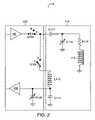
- FIG. 2is a block diagram of a transducer and related circuitry for transmitting and receiving according to certain principles of the present invention.
- FIG. 3is a circuit diagram including an adjustable varactor capacitor in which a transducer is tuned for receiving according to certain principles of the present invention.
- FIG. 4is a flow chart illustrating a method for adjusting a varactor capacitor and tuning a transducer for receiving according to certain principles of the present invention.
- FIG. 5is a circuit diagram including an adjustable varactor capacitor in which a transducer is tuned for transmitting according to certain principles of the present invention.
- FIG. 6is a flow chart illustrating a method for adjusting a varactor capacitor for transmitting over a transducer according to certain principles of the present invention.
- FIG. 7is a circuit including an adjustable transducer according to certain principles of the present invention.
- FIG. 8is a flow chart illustrating a method for adjusting a variable inductor transducer for transmitting according to certain principles of the present invention.
- FIG. 9is a circuit diagram including a capacitor bank for tuning a transducer device according to certain principles of the present invention.
- FIG. 10is a flow chart illustrating a method for adjusting a capacitance provided by a capacitor bank that tunes a transducer for transmitting according to certain principles of the present invention.
- FIG. 11is a circuit diagram including a first transducer for transmitting a wireless signal and second transducer for receiving a wireless signal according to certain principles of the present invention.
- FIG. 12is a flow chart illustrating a method for tuning a transducer according to certain principles of the present invention.
- FIG. 13is a circuit diagram of a transceiver system including multiple transducers for transmitting and receiving wireless signals according to certain principles of the present invention.
- FIG. 14is a flow chart illustrating a method for tuning a transducer for transmitting or receiving according to certain principles of the present invention.
- FIG. 15is a circuit diagram for tuning a transducer for receiving according to certain principles of the present invention.
- FIG. 16is a circuit diagram for tuning one of multiple transducers according to certain principles of the present invention.
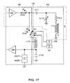
- FIG. 17is a circuit diagram for transmitting and receiving over one of multiple transducers according to certain principles of the present invention.
- FIG. 18is a circuit diagram for tuning one of multiple transducers according to certain principles of the present invention.
- FIG. 19is a diagram of a capacitor bank according to certain principles of the present invention.
- FIG. 20is a block diagram illustrating a wireless system for two-way communications according to certain principles of the present invention.
- FIG. 21is a circuit diagram illustrating a transceiver system for transmitting and receiving a wireless signal over a single transducer according to certain principles of the present invention.
- FIG. 22is a circuit diagram illustrating yet another transceiver system for transmitting and receiving a wireless signal over a single transducer according to the principles of the present invention.
- FIG. 23is a detailed circuit diagram illustrating a transceiver system for transmitting and receiving a wireless signal according to certain principles of the present invention.
- FIG. 24is a detailed circuit diagram illustrating a transceiver system according to certain principles of the present invention.
- FIG. 1is a block diagram illustrating a transceiver system according to certain principles of the present invention.
- a first transceiver 114is coupled via an inductive or magnetic field to second transceiver 165 .
- First transceiver 114is optionally portable so that its orientation is not fixed with respect to second transceiver 165 , which includes control circuit 161 and transducer 163 .
- Second transceiver 165itself can be portable while first transceiver is a fixed. Further, first transceiver 114 and second transceiver 165 both can be portable so that they are mobile and oriented in any manner with respect to each other.
- tuning circuit 144 and related circuitryis controlled by processor 142 to transmit over transducer 113 while tuning circuit 146 is controlled by processor 142 to receive over transducer 113 .
- Tuning informationcan be stored in memory 140 and retrieved by processor 142 for setting corresponding circuitry.
- transceivingtransmitting and/or receiving wireless signals according to the principles of the present invention are discussed relative to the following figures.
- FIG. 2is a block diagram illustrating a transducer for transmitting and receiving wireless signals according to certain principles of the present invention. As shown, a single transducer 113 can be employed to receive and transmit time-multiplexed wireless signals such as encoded magnetic fields.
- a single transducer 113can be tuned via impedance network 110 for transmitting and receiving at different times.
- transducer 113can be tuned to receive for a specified duration of time, while at other times, transducer 113 can be tuned to transmit for a duration of time.
- a single transducercan support bi-directional communications with one or multiple remote transceivers. The use of a single transducer supporting bi-directional communications can be particularly advantageous in space restricted applications.
- transducer 113can be an inductive device for generating a wireless signal such as a magnetic field.
- transducer 113can be a coiled strand of wire.
- a magnetic fieldcan be generated when a current is driven through the coiled wire.
- a ferrite rodcan be disposed at a core of the coiled strand of wire to enhance directional or signal strength characteristics of transducer 113 for receiving and transmitting a magnetic field.
- transducer 113includes a 3 ⁇ 25 mm (millimeters) ferrite rod having eight turns of wire.
- specific attributes of transducer 113can vary depending on a particular application.
- network 110includes capacitor C 111 , resistor R 112 , transducer 113 , capacitor C 114 , inductor L 115 , and capacitor C 116 .
- FIG. 1illustrates a specific network configuration including multiple electronic circuit elements for tuning transducer 113 , network 110 can be modified while still achieving the principles of the present invention.
- capacitors C 106 and C 116can be combined into one capacitor.
- resistor R 112is a model for the parasitic resistance of transducer 113 .
- the value of R 112can be dynamically controlled to change the operating efficiency, Q.
- R 112can be adjusted to change an effective bandwidth at which a tuned transducer transmits or receives a wireless signal. This can be achieved by switching additional resistors in parallel with R 112 .
- a transducer devicecan be tuned in two ways. First, a transducer can be tuned to transmit or receive over a wider or narrower bandwidth centered around a resonant frequency. Also, a transducer can be dynamically tuned to efficiently transmit or receive at a selected resonant frequency.
- a transduceris tuned to receive over a wide bandwidth while it is otherwise tuned to transmit over a narrower bandwidth.
- Such a transducer receiving over a wider bandwidthcan potentially receive wireless signals from multiple transceiver devices transmitting at different resonant frequencies without having to re-tune the transducer to each of the different resonant frequencies.
- Transceiver 100typically includes circuitry for transmitting and receiving over transducer 113 .
- transceiver 100can include transmitter amplifier 102 , switch S 104 , switch S 105 , capacitor C 106 , and receiver amplifier 108 .
- switch S 104 and switch S 105are both switched to the ‘T’ position and transmitter 102 drives transducer 113 and related circuitry as shown in FIG. 1 .
- Receiver circuit including L 115 , C 116 , C 106 , and receiver amplifier 108are generally disconnected (via open switch S 105 ) from transmitter circuit including amplifier 102 , S 104 , C 111 , C 114 , R 112 and transducer 113 while in a transmit mode.
- Switches S 104 and S 105can be electronically controlled BJT (Bipolar Junction Transistor) or FET (Field Effect Transistor) devices. When such devices are used, fast switching times can be achieved and transducer 113 can be quickly tuned to either transmit or receive. Consequently, a half duplex system including transducer 113 can be switched so fast that the system of the present invention appears to support full-duplex communications.
- BJTBipolar Junction Transistor
- FETField Effect Transistor
- switchesincluding mechanical devices such as relays, solenoids, and the like also can be used to switch between transmitting and receiving according to the principles of the present invention.
- switches S 104 and S 105are switched to the ‘T’ position for transmitting.
- S 104 and S 105are both generally switched to position ‘R’ and receiver 108 receives a signal sensed by transducer 113 .
- switches S 104 and S 105are driven by another electronic device controlled by, for example, a microprocessor that selects either transmitting or receiving.
- Receiver 108can be an amplifier device that senses a relatively small AC (Alternating Current) signal and amplifies it for further processing. For example, an amplitude varying voltage as sensed by transducer 113 can be amplified so that data such as digital information modulated onto a selected carrier frequency can be further processed by a microprocessor device. Receiver 108 can therefore be an amplifier device.
- ACAlternating Current
- one aspect of the present inventionconcerns tuning transducer 113 for transmitting and receiving at different intervals of time.
- a series LC circuitcan be tuned to a selected carrier frequency so that the impedance of transducer 113 is effectively reduced. More specifically, an overall reactance (as seen by transmitter 102 ) of combined circuitry C 111 , C 114 , R 112 , and transducer 113 can be effectively reduced so that a majority of energy is coupled to transducer 113 to generate a magnetic field. A portion of total energy will be dissipated by series resistor R 112 . However, the energy dissipated by R 112 is typically minimal and depends on the efficiency, Q, of the circuit.
- capacitor C 111Since a portion of the transmitter circuitry, i.e., capacitor C 111 , is in series with transducer 113 , its effects must be addressed while in the receive mode. For example, the capacitive effects of C 111 can be nullified by inductive effects of inductor L 115 when switches S 104 and S 105 are switched to receive mode.
- a parallel LC circuit including transducer 113generally can be tuned for optimal reception of a wireless signal such as a magnetic field.
- receiver circuitrycan be tuned to increase an effective impedance of transducer 113 so that a relatively large voltage develops at amplifier 108 as a result of a received wireless signal.
- a voltage generated by transducer 113 during receptioncan be coupled to input of receiver amplifier 108 , where the received signal is further amplified and digitally processed.
- an impedancesuch as a reactance along a receiver circuit path including C 111 , S 105 and L 115 between transducer 113 and receiver 108 is reduced for better signal reception, i.e., the circuit can be tuned to achieve a higher signal-to-noise ratio at receiver amplifier 108 .
- inductor L 115can be impedance matched to capacitor C 111 so that capacitors C 116 , C 114 , C 106 , and serial combination of R 112 and transducer 113 form a parallel tunable LC tank circuit.
- a substantial reactance of C 111 and L 115can cancel each other while switched to a receive mode.
- C 114can be effectively in parallel with C 106 and C 116 via a low impedance path including C 111 , S 105 and L 115 .
- C 111 and C 114are provided to tune transducer 113 . That is, a capacitance of C 111 and C 114 can be adjusted to cancel the inductive effects of transducer 113 .
- a ratio of C 111 to C 114is typically selected to set a peak current driving transducer 113 .
- Both C 114 and C 106can be tunable capacitors for adjusting the resonant frequency of corresponding transmit and receive circuits. Consequently, capacitors C 114 and C 106 can be electrically or mechanically tuned so that the corresponding circuit resonates at a particular carrier frequency.
- Transceiver device 112can be tested at a factory to determine optimal settings for capacitors C 106 and C 114 for transmitting and receiving at a particular carrier frequency. Either or both capacitors C 106 and C 114 can be fixed to permanent values in the factory. In one application, C 106 and C 114 are set or adjusted to a value during an assembly and testing process of a transceiver device and switches S 104 and S 105 are thereafter used to select a mode of transmitting or receiving.
- information concerning capacitor selectioncan be stored in memory and later retrieved to dynamically tune transducer 113 in the field depending on a particular application. More specifically, switch settings can be stored in a table and applied to select a capacitance of a particular capacitor bank to tune transducer 113 for transmitting or receiving at a particular carrier frequency. Information stored in memory can include binary data identifying which of multiple switches in a capacitor bank will be activated to select a particular capacitance of C 106 or C 114 .
- transmitter amplifier 102During transmission, transmitter amplifier 102 generates a voltage that couples across resistor R 112 and transducer 113 .
- transmitter 102generates an output at one of two voltages from an electronic device such as an ASIC (Application Specific Integrated Circuit).
- ASICApplication Specific Integrated Circuit
- transmitter 102can be designed to drive a binary voltage output of either 0 volts or 2 volts.
- data informationsuch as binary encoded data can be modulated onto a carrier frequency and transmitted over transducer 113 .
- a digital integrated circuit devicecan be used to drive transducer 113 .
- any other suitable voltagesuch as an analog sinusoidal voltage or other amplitude varying analog voltage can be used to effectively drive transducer 113 and related circuitry.
- a wireless signalcan be generated by transducer 113 for coupling to one or multiple target devices.
- transducer 113is tuned to transmit and receive at a resonant frequency of around 12.0 MHZ.
- a resonant frequencyof around 12.0 MHZ.
- any other suitable resonant frequencygenerally can be used.
- capacitor C 106 and C 114 as well as other components shown in FIG. 2can be adjustable to provide tuning of transducer 113 for either transmitting or receiving.
- an adjustable capacitoris formed via a bank of parallel capacitors C 1110 that are potentially connected to ground via corresponding switches S 1120 as shown in FIG. 19 .
- switchessuch as FET devices are activated to connect an end of a corresponding capacitor to ground.
- S 1120an effective capacitance of the bank increases.
- an overall capacitance supplied by the capacitor bankdecreases as capacitors are disconnected from ground via corresponding switches. Consequently, transducer 113 can be tuned to a particular resonant frequency by adjusting a reactance of circuits via switching for transmitting or receiving.
- switch setting informationcan be stored as binary data in memory.
- capacitor C 116can be selected to provide a majority of capacitance provided by combination of C 106 , C 114 and C 116 .
- one or multiple capacitors comprising C 106can be components having a smaller capacitance value to provide fine tuning of combined capacitance of C 106 and C 116 .
- C 111can be selected to provide a majority of capacitance provided by combination of C 111 and C 114 , while C 114 itself can be a capacitor bank comprising many smaller capacitors for fine tuning. Note that C 114 and C 111 are set to control the maximum signal strength.
- Another aspect of the present inventionconcerns selecting of components disposed in either the transmit or receive circuit.
- component valuesare typically selected to provide a desired performance.
- an actual size of componentsis a factor to consider for selecting component values.
- capacitor valuesare on the order of micro-farads or picoFarads.
- power dissipation and signal bandwidthare factors to consider for properly selecting component values.
- selection of componentscan differ depending on a particular application.
- transducer 113is selected to have a maximum number of effective ampere-turns so that a predetermined amount of power is dissipated in lumped loss element resistor R 112 .
- R 112represents a majority of losses in the transmit path.
- Transmitter 102 and each passive componenthas its own loss element but this is generally minimal.
- 12 MHZis a typical resonant frequency
- for transmitting or receiving a selected carrier frequencycan be any suitable setting such as between 0.5 and 60 MHZ.
- ⁇ 0the resonant frequency
- transducer 113can be 1.5 ⁇ H while C 111 and C 114 can be respectively 33 pF (picoFarads) and 84.3 pF.
- Efficiency factor, Qof the circuit can be approximately 40 depending on components selected resulting in resistance R 112 , inductance of transducer 113 (noted above as L 113 ), and capacitor divider C 111 and C 114 .
- the efficiency Qcan be defined as the energy stored by transducer 113 in its magnetic field divided by the energy dissipated by the overall transmitter circuit.
- RMSRoot Mean Squared
- V inoutput voltage of transmitter 102
- V 113voltage across transducer 113
- Typical values for the circuitare:
- transducer 113 impedanceOne factor to consider when selecting a transducer 113 impedance is electric field coupling between a remote transmitter and transducer 113 . For example, if the impedance of transducer 113 is too high, it produces signals as a result of electric field coupling (with remote transducers) rather than or in addition to magnetic field coupling. Typically, the inductance of transducer 113 is selected to substantially support inductive coupling. Thus, continuous coupling can be supported between transducer 113 and a remote device without nulls as sometimes experienced with RF devices.
- Component values for capacitorsare generally selected so they are larger than the parasitic capacitance of the circuit board and corresponding traces, including parasitic output capacitance of transmitter 102 and input capacitance of receiver 108 potentially disposed in an electronic device such as an ASIC (Application Specific Integrated Circuit).
- ASICApplication Specific Integrated Circuit
- inductor L 115is selected to cancel capacitive effects of C 111 .
- L 115is properly selected, a low impedance path is generally created so that C 114 , C 116 and C 106 are effectively in parallel with each other and transducer 113 .
- FIG. 3is a circuit diagram including an adjustable varactor capacitor in which a transducer is tuned for receiving according to certain principles of the present invention.
- FIG. 3includes adjustable varactor capacitor VC 106 (in lieu of C 106 ), bias generator 110 , resistor R 118 and capacitor C 120 .
- Transducer 113can be tuned for receiving based upon adjustments to varactor capacitor VC 106 .
- receiver amplifier 108can be coupled for receiving over transducer 113 by setting switches S 105 and S 104 to position ‘R’. While in the receive mode, an inductance of inductor L 115 approximately cancels a reactance of capacitor C 111 for effectively connecting transducer 113 via a low impedance path to capacitor C 116 and varactor capacitor VC 106 through resistor R 112 .
- Varactor capacitor VC 106 , capacitor C 116 , capacitor C 114 and transducer 113form a parallel tunable LC tank circuit in which varactor capacitor VC 106 is tuned to increase reception of a wireless signal as detected at the input of receiver amplifier 108 .
- Bias generator 110generates a voltage that is applied to VC 106 through resistor R 118 .
- the voltage of bias generator 110is adjusted to select a capacitance of VC 106 . Consequently, transducer 113 and related circuitry can be tuned to receive a wireless signal at a particular carrier frequency.
- Resistor 118provides resistive isolation between bias generator 110 and the received signal while capacitor C 120 provides DC (Direct Current) isolation between bias generator 110 and receiver amplifier 108 .
- bias generator 110can be controlled by many types of devices, bias generator 110 is typically a voltage source controlled by a microprocessor and related circuitry to adjust characteristics of the circuit and tune transducer 113 to receive at a particular carrier frequency.
- FIG. 4is a flow chart illustrating a method for adjusting a varactor capacitor and tuning a transducer for receiving according to certain principles of the present invention.
- transducer 113is coupled to receiver amplifier 108 by setting switch S 105 to position ‘R’.
- step 320transmitter amplifier 102 is decoupled from transducer 113 by setting switch S 104 to position ‘R’.
- step 330a wireless signal is received over transducer 113 .
- step 340the signal at input or output of receiver 108 is measured.
- step 350the capacitance of varactor capacitor VC 106 is adjusted via the voltage supplied by generator 110 to increase or maximize the received signal strength at the input of receiver amplifier 108 .
- this same procedurecan be utilized to set the transceiver device 112 in FIG. 2 for receiving.
- capacitor C 106 and C 114are adjusted for receiving at a particular carrier frequency.
- FIG. 5is a circuit diagram including an adjustable varactor capacitor in which a transducer is tuned for transmitting according to certain principles of the present invention.
- the circuit in FIG. 5is similar to that shown in FIG. 3 except varactor capacitor VC 114 , inductor L 117 , and capacitor C 120 are provided to adjust characteristics of the circuit for transmitting over transducer 113 .
- transmitter amplifier 102is switched for transmitting over transducer 113 by setting switch S 104 to position ‘T’ while receiver amplifier 108 is decoupled from transducer 113 and related circuitry by setting switch S 105 to position ‘T’.
- Capacitor C 111 , varactor capacitor VC 114 and transducer 113generally form a tunable LC circuit while in the transmit mode.
- varactor capacitor VC 106is adjusted to increase or maximize a transmit signal strength as measured at a magnetic loop probe located in proximity to transducer 113 .
- a voltage, Vs,is applied at inductor L 117 as shown to select a capacitance of VC 114 .
- This voltagecan be a DC voltage supplied from any suitable electronic device or component such as a D/A (Digital-to-Analog) converter.
- FIG. 5illustrates a specific technique for providing a bias to node V of VC 114
- other similar techniquescan be utilized to select an effective capacitance of VC 114 for tuning the circuit.
- Inductor L 117is typically provided to isolate voltage source Vs from VC 114 so that a signal supplied to transducer 113 is not effected by voltage supply, Vs.
- Capacitor C 120is a blocking capacitor that isolates DC (Direct Current) components of the voltage generated by voltage source Vs from appearing across transducer 113 .
- FIG. 6is a flow chart illustrating a method for adjusting a varactor capacitor for transmitting over a transducer according to certain principles of the present invention.
- transducer 113is coupled to transmitter 102 by setting switch S 104 to position ‘T’.
- step 520receiver amplifier 108 is decoupled from transducer 113 by setting switch S 105 to position ‘T’.
- step 525a signal is generated at transmitter 102 to transmit a wireless signal over transducer 113 .
- step 527the generated wireless signal is measured to determine a magnetic field strength.
- step 530the capacitance of varactor capacitor VC 114 is adjusted via a voltage supplied by source Vs to increase or maximize the transmitted signal from transducer 113 .
- a magnetic loop probecan be located in proximity to transducer 113 for monitoring a corresponding generated magnetic field.
- a range of voltagescan be applied to varactor capacitor VC 114 to determine which of multiple potential settings is preferred for transmitting data information at a particular carrier frequency.
- FIG. 7is a circuit including an adjustable transducer device according to certain principles of the present invention. Generally, adjustable transducer 213 is tuned for transmitting at a particular carrier frequency. Capacitor C 114 can be fixed instead of being adjustable as illustrated in previous figures.
- transmitter amplifier 102is coupled to transducer 213 by setting switch S 104 to position ‘T’ while receiver amplifier 108 is decoupled from variable inductor transducer 213 by setting switch S 105 to position ‘T’. While in this mode, capacitor C 111 , fixed capacitor C 114 and variable inductor antenna 113 generally form a tunable LC tank circuit.
- Variable inductor transducer 213can be adjusted to maximize or increase a magnetic field generated by transducer 213 .
- transducer 213can be adjusted while a monitor such as a magnetic loop probe located in proximity to transducer 213 monitors a wireless signal generated by transducer 213 to determine which of multiple potential settings is optimal for transmitting over adjustable transducer 213 .
- an inductance value of adjustable transducer 213can be varied manually or automatically.
- FIG. 8is a flow chart illustrating a method for adjusting a variable inductor transducer for transmitting according to certain principles of the present invention.
- transducer 213is coupled to transmitter 102 by setting switch S 104 to position ‘T’.
- step 720receiver amplifier 108 is decoupled from transducer 113 by setting switch S 105 to position ‘T’.
- step 725a signal is generated at transmitter 102 to transmit a wireless signal over transducer 213 .
- step 727the generated wireless signal is measured to determine a magnetic field strength.
- step 730the inductance of transducer 213 is adjusted to increase or maximize the wireless signal generated by transducer 213 .
- a magnetic loop probecan be located in proximity to transducer 213 for monitoring a corresponding generated magnetic field.
- transducer 213can be adjusted while the magnetic field is monitored to determine which of multiple potential settings is preferred for transmitting data information at a particular carrier frequency.
- FIG. 9is a circuit diagram including a capacitor bank for tuning a transducer device according to certain principles of the present invention. As shown, this circuit illustrates an embodiment including capacitors C 114 A . . . C 114 N and corresponding switches S 120 A . . . S 120 N for tuning transducer 113 .
- transmitter amplifier 102is coupled to transducer 113 by setting switch S 104 in position ‘T’ while receiver amplifier 108 is decoupled from transducer 113 by setting switch S 105 in the ‘T’ position.
- Capacitors 114 A . . . 114 Nform a capacitor bank and switches S 120 A . . . S 120 N form a switch bank that connect corresponding capacitors C 114 to ground.
- a switch S 120When a switch S 120 is closed, i.e., a low impedance path is provided between a corresponding capacitor and ground. An effective capacitance of the capacitor is then imparted at node P to increase the overall capacitance at node P. Conversely, when a switch S 120 is open, i.e., a high impedance path is provided between a corresponding capacitor and ground, a corresponding capacitor C 114 is effectively removed from the circuit so that this extra capacitance is no longer imparted at node P.
- switches S 120are FET (Field Effect Transistor) or BJT (Bipolar Junction Transistor) transistor devices controlled by a microprocessor device.
- FETField Effect Transistor
- BJTBipolar Junction Transistor
- any type of mechanical or electronic switchcan be used.
- Capacitor C 111selected capacitors C 114 (those coupled to ground via switches S 120 ) and transducer 113 form a tunable LC tank circuit.
- Capacitors C 114 A . . . C 114 Nare switched into and out of the circuit to maximize or increase a magnetic signal generated by transducer 113 .
- capacitor bank C 114 A . . . C 114 Ncan be adjusted while a monitor such as a magnetic loop probe located in proximity to transducer 113 monitors a signal generated by transducer 113 to determine which of multiple potential settings is optimal for transmitting.
- FIG. 10is a flow chart illustrating a method for adjusting a capacitance provided by a capacitor bank that tunes a transducer for transmitting according to certain principles of the present invention.
- transducer 113is coupled to transmitter 102 by setting switch S 104 to position ‘T’.
- step 920receiver amplifier 108 is decoupled from transducer 113 by setting switch S 105 to position ‘T’.
- step 925a signal is generated at transmitter 102 to transmit a wireless signal over transducer 113 .
- step 927the generated wireless signal is measured to determine a magnetic field strength.
- step 930the capacitance provided by capacitor bank C 114 is adjusted via switches S 120 to increase, maximize or optimize a magnetic signal transmitted from transducer 113 for a particular application.
- a magnetic loop probecan be located in proximity to transducer 113 for monitoring a corresponding generated magnetic field.
- a capacitance at node Pcan be adjusted while a magnetic field generated by transducer 113 is monitored. Consequently, settings for the circuit in FIG. 8 can be optimized for transmitting data information at a particular carrier frequency. These settings as discussed can be learned and then stored in memory.
- FIG. 11is a circuit diagram including transducers for transmitting a wireless signal and a transducer for receiving a wireless signal according to certain principles of the present invention.
- switch S 105can include multiple positions for coupling receiver 108 to either transducer X, transducer Y, transducer Z or loop 119 for receiving
- receiver circuitry including S 105 , L 115 , C 116 , C 106 and receiver 108can be duplicated for each of the transducers or wire loop 119 so that a magnetic signal can be received over a single selected transducer or multiple transducers simultaneously.
- second transducer 119can be positioned for receiving a wireless signal transmitted over transducer X, Y or Z, all of which are disposed in a single transceiver device.
- transducer 119is a wire loop antenna that enables self-tuning of a selected transducer based upon feedback.
- transducer 113can be tuned to transmit a wireless signal based on signal strength of the wireless signal as received at second transducer 119 .
- transducer 119 or transducer 113is fabricated from wire loops, coiled wires, wires, circuit board traces, discreet components, hybrid integrated circuit packages or monolithically integrated portions of integrated circuits. Any suitable transducer device can be employed for transmitting and receiving according to the principles of the present invention.
- switch S 105can include switch position settings XR, YR, and ZR as shown for respectively coupling a respective transducer X (transducer 113 ), Y or Z and related circuitry to an input of receiver 108 .
- Circuit 1050 and circuit 1060respectively include transducer Y and transducer Z and related circuitry that can be coupled to receiver 108 . Note that each transducer can be driven by a corresponding transmitter device as shown.
- switch S 104can be modified to include multiple switch positions so that transmitter 102 can drive a selected transducer.
- Switch position ‘L’ of switch S 105renders it possible to couple transducer 119 to the input of receiver 108 .
- a magnetic signal as transmitted by transducer X, Y or Zcan be monitored based on the wireless signal as received at transducer 119 .
- Feedback provided by transducer 119can be used to tune transducer 113 .
- capacitor C 114can be adjusted so that a maximal or increased magnetic field is generated by transducer 113 based on feedback from transducer 119 .
- the circuit as showncan be modified for properly receiving a corresponding wireless signal at receiver 108 .
- circuit 1050 and circuit 1060each can include a transducer similar to transducer 113 and corresponding circuitry for tuning.
- circuit 1050 and circuit 1060each can include a transducer device similar to transducer 113 .
- each circuit 1050 and circuit 1060can include corresponding components such as R 112 , C 114 , and C 111 , similar to the circuitry shown for transducer 113 .
- a corresponding transducercan be coupled via circuit path including L 115 , C 116 and C 106 to the input of receiver 108 .
- Capacitor C 106can be adjusted for tuning a transducer for receiving a wireless signal.
- a single receiver 108 and related circuitrycan be adjusted or tuned to receive a wireless signal over a selected one of multiple transducers.
- transducer X, Y or Zcan be adjusted for transmitting a corresponding wireless signal.
- transducers X, Y and Zare uniquely positioned so that they are orthogonal to each other.
- Transmitter amplifier 102can be coupled to transducer 113 by setting switch S 104 to position ‘T’ while transmitter amplifiers in circuits 1050 and 1060 are decoupled from their associated transducer Y and Z by setting their corresponding switches to an open position.
- Receiver 108is coupled to transducer 119 by setting switch S 105 to position ‘L’. However, after an optimal setting is identified for transmitting over a particular transducer, switch S 105 can be switched to receive on one of the other transducers. Thus, receiver 108 also can be switched to receive a wireless signal from a remotely located source.
- a combination of capacitor C 111 , capacitor C 114 and transducer 113form a tunable LC circuit, in which capacitor C 114 is tuned to maximize or increase the magnetic signal strength as generated by transducer 113 .
- Transducer 119is typically positioned in reasonable proximity such as within centimeters or millimeters of transducer 113 for receiving the corresponding wireless signal generated by transducer 113 .
- the strength of the received wireless signalcan be measured at the output of receiver amplifier 108 .
- This feedback processalso can be used to tune transducer Y or transducer Z when switches are set to YT or ZT respectively.
- each transducer deviceis uniquely positioned with respect to each other.
- three transducerssuch as transducers X, Y, and Z can be orthogonally disposed to each other along an X, Y and Z axis for transmitting and receiving one or multiple wireless signals. Based upon this configuration, a continuous wireless link can be supported with a remote target device such as that shown in FIG. 1 , even though an orientation of transducers changes as a result of motion.
- FIG. 12is a flow chart illustrating a method for tuning a transducer according to certain principles of the present invention.
- transducer 113is coupled to transmitter amplifier 102 by setting switch S 104 to position ‘XT’.
- receiver amplifier 108is coupled to transducer 119 by setting switch S 105 to position ‘L’.
- Transducer 119can be tuned to receive at the same carrier frequency as the magnetic field transmitted by transducer 113 . This can be achieved by adjusting capacitance of C 116 .
- transducer 119is tested at a factory and preferred capacitance settings for each of multiple carrier frequencies are recorded in memory for later use. For example, transducer 119 is exposed to a wireless signal having a known carrier frequency and capacitance C 106 is adjusted so that a maximal signal is received at receiver 108 . Thus, transducer 119 can thereafter be tuned for optimally receiving a wireless signal at the carrier frequency based on capacitor settings as stored in memory.
- step 1122a wireless signal is transmitted over transducer 113 .
- step 1124part of this transmitted signal is received over transducer 119 .
- step 1126the wireless signal as received over transducer 119 is measured at receiver 108 .
- capacitor C 114is adjusted so that an increased or maximal signal as generated by transducer 113 is received at the input of receiver amplifier 108 for a particular carrier frequency.
- the strength of the wireless signal generated by transducer 113 as received at receiver 108can be measured for tuning transducer 113 .
- the voltage level of the received signal at receiver 108can indicate a relative signal strength of the received magnetic field generated by transducer 113 .
- Other methods of measuring the power level of the wireless signalalso can be employed to provide a relative measure of received signal strength.
- transducer 113Based on a power level of the received magnetic field at transducer 119 , transducer 113 can be tuned to transmit an increased signal.
- capacitor C 114can be swept through a range of potential capacitance settings so that an optimal setting can be identified for a particular environment in which the transceiver device operates. Accordingly, settings can be learned and stored in memory for later use.
- FIG. 13is a circuit diagram of a transceiver system including multiple transducers for transmitting and receiving wireless signals according to certain principles of the present invention.
- switch S 105can be set to receive over either transducer X (transducer 113 ), transducer Y or transducer Z.
- Circuitry 150 for driving transducer 113 (transducer X)can be duplicated in circuits 1050 and 1060 for transmitting over transducer Y or Z as previously discussed. Accordingly, one of multiple transducers in a transducer device can be selected for transmitting while a different transducer can be selected for receiving. As discussed, one purpose for tuning a selected transducer is to increase its generated field strength.
- transmitter amplifier 102is coupled to transmit over transducer 113 by setting switch S 104 to position ‘XT’ while a second transducer is selected via switch S 105 to receive a wireless signal for tuning transducer 113 .
- switch S 105 as shownis set to position ‘YR’ for receiving over transducer Y.
- switch S 105can be set to optional position T, thus disconnecting receiver 108 from all transducers to reduce power consumption or circuit interference.
- receiver 108is coupled to receive over transducer Y and switch S 104 is set to position ‘YR’ as shown.
- capacitor C 111 , capacitor C 114 and transducer 113form a tunable LC circuit, in which capacitor C 114 is tuned to transmit at an optimal signal strength.
- a magnetic signalcan be transmitted over transducer 113 while attributes of the transmitted magnetic signal are received and monitored over transducer Y.
- transducer 113can be tuned to optimally transmit based on feedback received at transducer Y.
- a receiving transducer and related circuitrycan be adjusted to optimally receive a signal that is transmitted by a selected transducer.
- capacitor C 106can be adjusted to optimally receive a wireless signal as generated by transducer X.
- transducer orientationcan effect whether a signal is detected. If the transmitted magnetic signal does not couple to transducer Y due to its orientation, another transducer can be selected to monitor the wireless signal from the transducer X. For example, switch S 105 can be switched to receive over transducer Z instead of transducer Y if no signal is detected.
- transducersare typically located within less than several inches from each other, coupling is very likely for all transducers even when the transducers are positioned substantially orthogonal to each other.
- any one of multiple transducerscan be tuned for optimally transmitting or receiving during field use. That is, a transceiver device need not be returned to the factory for testing and adjusting characteristics of the circuit. It can be adjusted during normal operational use of the transceiver device.
- a transceiver device incorporating the principles of the present inventioncan adapt itself to provide optimal, improved or continuous coupling with a remote device despite operation of the device in an ever-changing environment.
- a power supply energizing the transceiverwill last longer because the transceiver device is optimally linked to a target device. More specifically, circuits can be tuned so that minimal energy is dissipated while generating a maximum magnetic field.
- FIG. 14is a flow chart illustrating a method for tuning a transducer for transmitting or receiving according to certain principles of the present invention.
- transducer 113is coupled to transmitter amplifier 102 by setting switch S 104 to position ‘XT’.
- receiver amplifier 108is coupled to transducer Y by setting switch S 105 to position ‘YR’.
- transducer YRis tuned to receive at the same carrier frequency as transmitted by transducer 113 . This can be achieved by adjusting capacitance at C 106 .
- step 1322a wireless signal is transmitted over transducer X.
- step 1324the transmitted signal from transducer X is received over transducer Y.
- step 1326the signal as received over transducer Y is measured at receiver 108 .
- step 1330a capacitance provided by capacitor C 114 is adjusted so that an increased, optimal or maximal signal as generated by transducer X is received at the input of receiver amplifier 108 for a particular carrier frequency.
- step 1340a wireless signal is transmitted over transducer X.
- a capacitance of C 106can be adjusted so that transducer Y and related circuitry is tuned for optimally receiving. For example, transducer Y and related circuitry are adjusted to optimally receive a wireless signal transmitted by transducer X.
- the strength of the wireless signal generated by transducer 113 as received at receiver 108 over transducer Yis optionally measured for tuning transducer 113 or transducer Y.
- the voltage level of the received signal at receiver 108can indicate a relative signal strength of the received magnetic field generated by transducer 113 .
- Other methods of measuring the power level of the wireless signalalso can be employed to provide a relative measure of received signal strength.
- transducer X, transducer Y, or transducer Zcan be selectively tuned to transmit or receive an increased magnetic signal.
- capacitor C 114 or C 106can be swept through a range of potential capacitance settings to learn which setting is optimal for transmitting or receiving over a corresponding transducer.
- FIG. 15is a circuit diagram for tuning a transducer for receiving according to certain principles of the present invention. As shown, transducer 118 is provided for generating a magnetic field that is received over selected transducer 113 .
- receiver amplifier 108 of transceiver 100is coupled to transducer 113 by setting switch S 105 to position ‘XR’ while transmitter amplifier 102 is decoupled from transducer 113 by setting switch S 104 to position ‘R’.
- Transmitter 117is coupled to transducer 118 through capacitor 120 when switch S 103 is set to position ‘T’.
- capacitor C 106can be adjusted to tune transducer 113 for receiving a wireless signal generated by transducer 118 . Specifically, capacitor C 106 can be swept through a range of potential capacitance settings to determine which setting provides an optimal setting for receiving over transducer 113 .
- Switch S 105also can be switched to select a mode for receiving over transducer Y or Z.
- transducer Y or Zcan be optimally tuned for receiving a wireless signal generated by transducer 118 .
- FIG. 16is a circuit diagram for tuning one of multiple transducers according to certain principles of the present invention. As shown, separate circuits are provided for transmitting and receiving over a corresponding transducer. For example, circuit 185 is dedicated to transducer 113 for transmitting and receiving. Circuit 186 and circuit 187 include similar components as shown for circuit 185 . However, circuit 186 and 187 are employed to receive and transmit over transducer Y of circuit 186 and transducer Z of circuit 187 , respectively. In other words, circuit 185 can be replicated for transmitting and receiving over multiple transducers.
- Circuitry including receiver 108 , switch S 110 , capacitor bank C 4010 and switch bank S 4020can be disposed so that they are common to all circuits.
- switch S 110can be switched to receive over one of multiple transducers such as orthogonally positioned transducers X, Y and Z.
- receiver 108is coupled to transducer Y. Since a portion of circuitry is shared among transducers, specific circuitry such as capacitor bank C 4010 , receiver 108 and switch bank S 4020 are not needlessly duplicated for each circuit.
- switch S 105in a transmit mode, switch S 105 as well as complementary switches disposed in circuit 186 and circuit 187 can be set to position ‘T’ for decoupling receiver 108 from a corresponding transducer.
- a single transducer or multiple transducerscan be tuned and driven at the same time using a common carrier frequency or different carrier frequencies.
- a selected one of multiple transducerscan be individually tuned for receiving a wireless signal via coupling provided by switch S 110 .
- FIG. 17is a circuit diagram for transmitting and receiving over one of multiple transducers according to certain principles of the present invention. As shown, minimal circuit components can be employed to tune a transducer for transmitting or receiving at a particular carrier frequency.
- Switch S 105selects which of multiple transducers such as transducer X, transducer Y (in circuit 196 ) or transducer Z (in circuit 197 ) will be tuned for receiving at receiver 108 .
- Common circuitry shared by the multiple transducersincludes receiver 108 , capacitor bank C 4010 , switch bank S 4020 , C 116 and L 115 .
- the circuitry shown in circuit 195can be replicated in circuit 196 to receive/transmit over transducer Y and circuit 197 to receive/transmit over transducer Z.
- switch S 104 or its complement in circuit 196 or 197is set to position ‘T’ while switch S 105 is set to receive over another transducer.
- transmitter 102is coupled to drive transducer X while receiver 108 is coupled to receive over transducer Y.
- a selected transducercan be tuned for optimally transmitting or receiving a wireless signal.
- This technique of adjusting each transducer via capacitance provided by capacitor bank 4010simplifies tuning multiple transducers, each of which potentially has its own unique electronic characteristics. For example, electronic characteristics of transducer devices can vary from component to component as a result of manufacturing tolerances. Consequently, a single adjustable circuit can be adjusted to dynamically tune each of multiple unique transducer devices for receiving or transmitting.
- FIG. 18is a circuit diagram for tuning one of multiple transducers according to certain principles of the present invention. As shown, minimal circuit components can be employed to tune a selected transducer for transmitting or receiving at a particular carrier frequency. Components in circuit 175 including C 111 , C 114 , R 112 and transducer 113 (transducer X) can be duplicated in circuit 176 and circuit 177 . Circuit 176 includes transducer Y while circuit 177 includes transducer Z.
- Switch S 105can be switched to select which, if any, of multiple receivers will be coupled to receiver 108 for receiving. As shown, switch S 105 is set to position YP for receiving a wireless signal over transducer Y.
- switch S 104can be switched to select which, if any, of multiple transducers will be coupled to transmitter 102 for transmitting.
- one transducercan be tuned for transmitting while another transducer can be tuned for receiving.
- FIG. 20is a block diagram illustrating a wireless system for two-way communications according to certain principles of the present invention. The techniques as previously discussed can be used in this embodiment to dynamically tune a transducer dedicated for either transmitting or receiving.
- transceiver device 2010 and transceiver device 2060communicate with each other via wireless signals.
- Each transceiver devicecan include at least one dedicated transmitter 2030 , 2085 (transducer and related circuitry) for transmitting a wireless signal and at least one dedicated receiver 2035 , 2080 (transducer and related circuitry) for receiving.
- a switchcan be provided so that one of multiple uniquely oriented transducer devices within a transmitter or receiver can be selected and dynamically tuned for transmitting or receiving a wireless signal as previously discussed.
- processor 2015In a forward direction between transceiver 2010 and transceiver 2060 , processor 2015 generates encoded data and transmits a wireless signal from transmitter 2030 at a selected carrier frequency. For example, a dedicated transducer of transmitter 2030 can be dynamically tuned to transmit at a selected carrier frequency. Receiver 2080 is dynamically tuned to receive at the selected carrier frequency and decode the received wireless signal at processor 2065 .
- processor 2065In a reverse direction, processor 2065 generates encoded data and transmits a wireless signal from transmitter 2085 at a dynamically selected carrier frequency. Receiver 2035 is dynamically tuned to receive over the selected carrier frequency and decode the received wireless signal at processor 2015 .
- a first carrier frequencycan be utilized to transmit/receive information in one direction while a different carrier frequency can be used to transmit/receive information in the opposite direction.
- Time division multiplexing techniquesalso can be used to transmit and receive information over a commonly used carrier frequency.
- a single dedicated transducer devicecan be dynamically or electronically tuned for transmitting or receiving at a particular carrier frequency.
- interferencetypically can be avoided during operational use in the field by dynamically tuning a transmitter/receiver pair of the transducers to transmit and receive at another carrier frequency.
- FIG. 21is a circuit diagram illustrating a transceiver system for transmitting and receiving a wireless signal over a single transducer according to certain principles of the present invention. As shown, certain circuit elements have been eliminated from the transceiver system as shown in FIG. 2 . More specifically, inductor L 115 and capacitors C 106 and C 116 have been eliminated.
- the transceiver system as shown in FIG. 21supports two-way communication over a single transducer device using fewer circuit components. Consequently, the wireless communication system according to the principles of the present invention can occupy a smaller volume and thus fit into yet smaller wireless transceiver devices.
- both switches S 104 and S 105are set to position T.
- Capacitor C 114is adjusted to tune transducer 113 for transmitting at a selected carrier frequency similar to the circuits as previously discussed.
- both switches S 104 and S 105are set to position R.
- Capacitor C 114is adjusted to tune transducer 113 for receiving at a selected carrier frequency.
- a voltage proportional to a received wireless signal at transducer 113is generated at the node connecting C 111 , C 114 and R 112 . This generated voltage or signal is coupled to receiver amplifier 108 through the circuit path including switch S 105 and capacitor C 111 .
- FIG. 22is a circuit diagram illustrating yet another transceiver system for transmitting and receiving a wireless signal over a single transducer according to certain principles of the present invention.
- adjustable capacitor C 114 and switch S 104have been eliminated from the diagram as shown in FIG. 21 .
- capacitor C 111has been modified so that it is adjustable.
- the circuitincludes only one switch that must be controlled for selecting either a transmit or receive mode.
- switch S 105is set to position T.
- capacitor C 111is adjusted to tune transducer 113 for transmitting at a selected carrier frequency.
- Transmitter 102is controlled to produce an output voltage and drive transducer 113 .
- switch S 105is set to position R and the output of transmitter 102 is driven to a virtual ground.
- capacitor C 111is effectively disposed in parallel with the combination of R 112 and transducer 113 . Similar to the principles as previously discussed, capacitor C 111 is adjusted to tune transducer 113 for receiving at a selected carrier frequency.
- a voltage proportional to a received wireless signalis generated at the node connecting C 111 , R 112 and S 105 . The generated voltage or signal is coupled to receiver amplifier 108 through the low impedance circuit path including switch S 105 .
- FIG. 23is a detailed circuit diagram illustrating a transceiver system for transmitting and receiving a wireless signal according to certain principles of the present invention. Generally, FIG. 23 is a more detailed circuit diagram illustrating a system and method for providing an adjustable capacitance at C 111 as shown in FIG. 22 .
- a capacitor bank including capacitor C 230 - 1 , C 230 - 2 , C 230 - 3 . . . C 230 -nare selectively coupled to the output of transmitter 102 via corresponding switches S 240 - 1 , S 240 - 2 , S 240 - 3 . . . S 240 -n. Similar to the principles as previously discussed, characteristics of the circuit are adjusted to tune transducer 113 for transmitting or receiving. More specifically, capacitors C 230 are switched in and out to adjust a combined capacitance of C 111 for transmitting or receiving a wireless signal over transducer 113 .
- FIG. 24is a detailed circuit diagram illustrating a transceiver system for transmitting and receiving a wireless signal according to certain principles of the present invention.
- C 2410is a DC blocking capacitor to keep DC voltages from input of receiver 108 .
- C 2420can be used to shift the resonant frequency of the receiver (e.g., from 12 to 13 MHz) while R 2430 can be adjusted to change the Q of the receiver 108 .
- This tuning circuitcan ensure that the proper impedance is present at the frequency of use. This may be necessary due to variations in the coil impedance.
- a variable capacitor C 106can be used for tuning the receiver. This can be achieved in manufacturing by monitoring the received signal strength and adjusting capacitor C 106 .
- Automatic tuning of transducer 113 for receiving on receiver 108can be achieved using a firmware driven capacitor table containing multiple programmable capacitors with 40 pF of range. This capacitor table can be loaded into memory when a transceiver system 2400 is turned on.
- transceiver system 2400is a TDD (Time Division Duplex) system that can be configured to alternately transmit and receive in synchronization with a base transceiver unit.
- switch S 105is open and one or more of transmitter drivers 102 - 1 . . . 102 -n can be selectively activated (to control power output levels) and to apply a 50% duty GMSK modulated square wave to transducer 113 and related circuitry.
- This front-end network, including transducer 113 , and impedance scaling capacitorsform a series tuned band pass filter that is centered at the carrier frequency. The result is a GMSK modulated sine wave coil current.
- a low impedance of the transmitter driver 102can be removed from the circuit. This can be accomplished by setting the drivers to a high output impedance state.
- Switch S 105can be closed and the receiver tuning network switches associated with C 106 can be adjusted. In this mode, the series tuned band pass response of the transmitter path has been converted into a purely parallel band pass response.
Landscapes
- Engineering & Computer Science (AREA)
- Signal Processing (AREA)
- Computer Networks & Wireless Communication (AREA)
- Physics & Mathematics (AREA)
- Electromagnetism (AREA)
- Near-Field Transmission Systems (AREA)
- Transceivers (AREA)
- Circuits Of Receivers In General (AREA)
Abstract
Description
Given a carrier frequency generally centered around 12.0 MHZ,
PR112=(I113)2·R112
where
Claims (20)
Priority Applications (1)
| Application Number | Priority Date | Filing Date | Title |
|---|---|---|---|
| US11/544,950US7574173B2 (en) | 2001-03-16 | 2006-10-06 | Wireless communication over a transducer device |
Applications Claiming Priority (5)
| Application Number | Priority Date | Filing Date | Title |
|---|---|---|---|
| US27639801P | 2001-03-16 | 2001-03-16 | |
| US29622901P | 2001-06-06 | 2001-06-06 | |
| US94237201A | 2001-08-29 | 2001-08-29 | |
| US10/004,989US7142811B2 (en) | 2001-03-16 | 2001-12-03 | Wireless communication over a transducer device |
| US11/544,950US7574173B2 (en) | 2001-03-16 | 2006-10-06 | Wireless communication over a transducer device |
Related Parent Applications (1)
| Application Number | Title | Priority Date | Filing Date |
|---|---|---|---|
| US10/004,989ContinuationUS7142811B2 (en) | 2001-03-16 | 2001-12-03 | Wireless communication over a transducer device |
Publications (2)
| Publication Number | Publication Date |
|---|---|
| US20070082611A1 US20070082611A1 (en) | 2007-04-12 |
| US7574173B2true US7574173B2 (en) | 2009-08-11 |
Family
ID=27485422
Family Applications (2)
| Application Number | Title | Priority Date | Filing Date |
|---|---|---|---|
| US10/004,989Expired - LifetimeUS7142811B2 (en) | 2001-03-16 | 2001-12-03 | Wireless communication over a transducer device |
| US11/544,950Expired - LifetimeUS7574173B2 (en) | 2001-03-16 | 2006-10-06 | Wireless communication over a transducer device |
Family Applications Before (1)
| Application Number | Title | Priority Date | Filing Date |
|---|---|---|---|
| US10/004,989Expired - LifetimeUS7142811B2 (en) | 2001-03-16 | 2001-12-03 | Wireless communication over a transducer device |
Country Status (4)
| Country | Link |
|---|---|
| US (2) | US7142811B2 (en) |
| EP (1) | EP1378070A2 (en) |
| AU (1) | AU2002254243A1 (en) |
| WO (1) | WO2002075939A2 (en) |
Cited By (34)
| Publication number | Priority date | Publication date | Assignee | Title |
|---|---|---|---|---|
| US20090041241A1 (en)* | 2007-08-08 | 2009-02-12 | Radeum, Inc. | Near field communications system having enhanced security |
| US20090098827A1 (en)* | 2007-08-30 | 2009-04-16 | Kyocera Corporation | Communication apparatus and method for controlling the same |
| US20110278945A1 (en)* | 2010-05-13 | 2011-11-17 | Qualcomm Incorporated | Resonance detection and control within a wireless power system |
| US20120252362A1 (en)* | 2011-03-28 | 2012-10-04 | Felica Networks, Inc. | Communication device |
| US8880100B2 (en) | 2011-03-23 | 2014-11-04 | Radium, Inc. | Proximity based social networking |
| US8929809B2 (en) | 2011-03-22 | 2015-01-06 | Radeum, Inc. | Techniques for wireless communication of proximity based content |
| US9287040B2 (en) | 2012-07-27 | 2016-03-15 | Thoratec Corporation | Self-tuning resonant power transfer systems |
| US9397726B2 (en) | 2010-08-23 | 2016-07-19 | Radeum, Inc. | System and method for communicating between near field communication devices within a target region using near field communication |
| US9400985B2 (en) | 2010-11-08 | 2016-07-26 | Radeum, Inc. | Techniques for wireless communication of proximity based content |
| US9583874B2 (en) | 2014-10-06 | 2017-02-28 | Thoratec Corporation | Multiaxial connector for implantable devices |
| US9592397B2 (en) | 2012-07-27 | 2017-03-14 | Thoratec Corporation | Thermal management for implantable wireless power transfer systems |
| US9621227B2 (en) | 2014-08-29 | 2017-04-11 | Freelinc Technologies | Proximity boundary based communication using radio frequency (RF) communication standards |
| US9680310B2 (en) | 2013-03-15 | 2017-06-13 | Thoratec Corporation | Integrated implantable TETS housing including fins and coil loops |
| US9805863B2 (en) | 2012-07-27 | 2017-10-31 | Thoratec Corporation | Magnetic power transmission utilizing phased transmitter coil arrays and phased receiver coil arrays |
| US9825471B2 (en) | 2012-07-27 | 2017-11-21 | Thoratec Corporation | Resonant power transfer systems with protective algorithm |
| US9855437B2 (en) | 2013-11-11 | 2018-01-02 | Tc1 Llc | Hinged resonant power transfer coil |
| US10148126B2 (en) | 2015-08-31 | 2018-12-04 | Tc1 Llc | Wireless energy transfer system and wearables |
| US10164685B2 (en) | 2014-12-31 | 2018-12-25 | Freelinc Technologies Inc. | Spatially aware wireless network |
| US10177604B2 (en) | 2015-10-07 | 2019-01-08 | Tc1 Llc | Resonant power transfer systems having efficiency optimization based on receiver impedance |
| US10186760B2 (en) | 2014-09-22 | 2019-01-22 | Tc1 Llc | Antenna designs for communication between a wirelessly powered implant to an external device outside the body |
| US10251987B2 (en) | 2012-07-27 | 2019-04-09 | Tc1 Llc | Resonant power transmission coils and systems |
| US10291067B2 (en) | 2012-07-27 | 2019-05-14 | Tc1 Llc | Computer modeling for resonant power transfer systems |
| US10373756B2 (en) | 2013-03-15 | 2019-08-06 | Tc1 Llc | Malleable TETs coil with improved anatomical fit |
| US10383990B2 (en) | 2012-07-27 | 2019-08-20 | Tc1 Llc | Variable capacitor for resonant power transfer systems |
| US10525181B2 (en) | 2012-07-27 | 2020-01-07 | Tc1 Llc | Resonant power transfer system and method of estimating system state |
| US10610692B2 (en) | 2014-03-06 | 2020-04-07 | Tc1 Llc | Electrical connectors for implantable devices |
| US10615642B2 (en) | 2013-11-11 | 2020-04-07 | Tc1 Llc | Resonant power transfer systems with communications |
| US10695476B2 (en) | 2013-11-11 | 2020-06-30 | Tc1 Llc | Resonant power transfer systems with communications |
| US10770923B2 (en) | 2018-01-04 | 2020-09-08 | Tc1 Llc | Systems and methods for elastic wireless power transmission devices |
| US10898292B2 (en) | 2016-09-21 | 2021-01-26 | Tc1 Llc | Systems and methods for locating implanted wireless power transmission devices |
| US11197990B2 (en) | 2017-01-18 | 2021-12-14 | Tc1 Llc | Systems and methods for transcutaneous power transfer using microneedles |
| US12057896B2 (en) | 2020-05-07 | 2024-08-06 | Cascodium Llc | Devices, systems and methods for sensing and tracing proximity contacts |
| US12096167B2 (en) | 2019-01-30 | 2024-09-17 | Fraunhofer-Gesellschaft Zur Foerderung Der Angewandten Forschung E.V. | Bidirectional configuration of sensor nodes with mobile phone with no extension |
| US12294422B2 (en) | 2019-05-10 | 2025-05-06 | Fraunhofer-Gesellschaft zur Förderung der angewandten Forschung e.V. | Efficient communication to configure sensor nodes |
Families Citing this family (110)
| Publication number | Priority date | Publication date | Assignee | Title |
|---|---|---|---|---|
| US7657297B2 (en)* | 2004-05-03 | 2010-02-02 | Dexcom, Inc. | Implantable analyte sensor |
| US8744384B2 (en) | 2000-07-20 | 2014-06-03 | Blackberry Limited | Tunable microwave devices with auto-adjusting matching circuit |
| US8064188B2 (en) | 2000-07-20 | 2011-11-22 | Paratek Microwave, Inc. | Optimized thin film capacitors |
| JP3727853B2 (en)* | 2001-01-26 | 2005-12-21 | 三菱電機株式会社 | In-vehicle device for narrow area communication |
| US7035608B2 (en)* | 2001-03-16 | 2006-04-25 | Aura Communications Technology, Inc. | Methods and apparatus for tuning in an inductive system |
| US7532901B1 (en) | 2001-03-16 | 2009-05-12 | Radeum, Inc. | Methods and apparatus to detect location and orientation in an inductive system |
| US7920906B2 (en) | 2005-03-10 | 2011-04-05 | Dexcom, Inc. | System and methods for processing analyte sensor data for sensor calibration |
| US7818036B2 (en)* | 2003-09-19 | 2010-10-19 | Radeum, Inc. | Techniques for wirelessly controlling push-to-talk operation of half-duplex wireless device |
| US7149552B2 (en)* | 2003-09-19 | 2006-12-12 | Radeum, Inc. | Wireless headset for communications device |
| US7818037B2 (en)* | 2003-09-19 | 2010-10-19 | Radeum, Inc. | Techniques for wirelessly controlling push-to-talk operation of half-duplex wireless device |
| US9247900B2 (en) | 2004-07-13 | 2016-02-02 | Dexcom, Inc. | Analyte sensor |
| US7325180B2 (en)* | 2003-11-26 | 2008-01-29 | Carnegie Mellon University | System and method to test integrated circuits on a wafer |
| US7515881B2 (en)* | 2003-11-26 | 2009-04-07 | Starkey Laboratories, Inc. | Resonance frequency shift canceling in wireless hearing aids |
| US8423114B2 (en) | 2006-10-04 | 2013-04-16 | Dexcom, Inc. | Dual electrode system for a continuous analyte sensor |
| ATE480761T1 (en) | 2003-12-05 | 2010-09-15 | Dexcom Inc | CALIBRATION METHODS FOR A CONTINUOUSLY WORKING ANALYTICAL SENSOR |
| US11633133B2 (en) | 2003-12-05 | 2023-04-25 | Dexcom, Inc. | Dual electrode system for a continuous analyte sensor |
| US8792955B2 (en) | 2004-05-03 | 2014-07-29 | Dexcom, Inc. | Transcutaneous analyte sensor |
| US7654956B2 (en) | 2004-07-13 | 2010-02-02 | Dexcom, Inc. | Transcutaneous analyte sensor |
| EP1679937A1 (en)* | 2005-01-06 | 2006-07-12 | IDT Sonicvision Limited | Wireless output system for audio/video equipment |
| US20060150221A1 (en)* | 2005-01-06 | 2006-07-06 | Idt Sonicvision Limited | Wireless output system for audio/video equipment |
| US8249500B2 (en)* | 2005-02-24 | 2012-08-21 | Innovision Research & Technology Plc | Tuneable NFC device |
| US9406444B2 (en) | 2005-11-14 | 2016-08-02 | Blackberry Limited | Thin film capacitors |
| US8125399B2 (en) | 2006-01-14 | 2012-02-28 | Paratek Microwave, Inc. | Adaptively tunable antennas incorporating an external probe to monitor radiated power |
| US7711337B2 (en) | 2006-01-14 | 2010-05-04 | Paratek Microwave, Inc. | Adaptive impedance matching module (AIMM) control architectures |
| US8325097B2 (en) | 2006-01-14 | 2012-12-04 | Research In Motion Rf, Inc. | Adaptively tunable antennas and method of operation therefore |
| US9130602B2 (en) | 2006-01-18 | 2015-09-08 | Qualcomm Incorporated | Method and apparatus for delivering energy to an electrical or electronic device via a wireless link |
| US8447234B2 (en)* | 2006-01-18 | 2013-05-21 | Qualcomm Incorporated | Method and system for powering an electronic device via a wireless link |
| WO2007107642A1 (en) | 2006-03-21 | 2007-09-27 | Tmms Co., Ltd. | Device for transporting energy by partial influence through a dielectric medium |
| US7647035B2 (en)* | 2006-09-15 | 2010-01-12 | Broadcom Corporation | RF transceiver with undesired signal rejection and methods for use therewith |
| US20080076476A1 (en)* | 2006-09-22 | 2008-03-27 | Broadcom Corporation, A California Corporation | RF transceiver with a plurality of programmable antennas and methods for use therewith |
| US7639199B2 (en)* | 2006-09-22 | 2009-12-29 | Broadcom Corporation | Programmable antenna with programmable impedance matching and methods for use therewith |
| US7848386B2 (en)* | 2006-09-22 | 2010-12-07 | Broadcom Corporation | Frequency hopping RF transceiver with programmable antenna and methods for use therewith |
| US20080076353A1 (en)* | 2006-09-26 | 2008-03-27 | Broadcom Corporation, A California Corporation | Cable modem with integrated RF identification and methods for use therewith |
| US20080076354A1 (en)* | 2006-09-26 | 2008-03-27 | Broadcom Corporation, A California Corporation | Cable modem with programmable antenna and methods for use therewith |
| US20080123568A1 (en)* | 2006-09-26 | 2008-05-29 | Broadcom Corporation, A California Corporation | Cable modem with wireless voice-over-IP phone and methods for use therewith |
| US20100321128A1 (en)* | 2006-10-19 | 2010-12-23 | Nxp, B.V. | Transceiving circuit for contactless communication |
| US8299867B2 (en)* | 2006-11-08 | 2012-10-30 | Research In Motion Rf, Inc. | Adaptive impedance matching module |
| US7714676B2 (en) | 2006-11-08 | 2010-05-11 | Paratek Microwave, Inc. | Adaptive impedance matching apparatus, system and method |
| US7535312B2 (en)* | 2006-11-08 | 2009-05-19 | Paratek Microwave, Inc. | Adaptive impedance matching apparatus, system and method with improved dynamic range |
| US9582981B2 (en)* | 2014-10-08 | 2017-02-28 | Rfmicron, Inc. | Radio frequency identification (RFID) moisture tag(s) and sensors with extended sensing via capillaries |
| US11817637B2 (en) | 2006-11-18 | 2023-11-14 | Rfmicron, Inc. | Radio frequency identification (RFID) moisture tag(s) and sensors with extended sensing via capillaries |
| US20080174500A1 (en)* | 2007-01-23 | 2008-07-24 | Microsoft Corporation | Magnetic communication link with diversity antennas |
| US8539809B2 (en)* | 2007-01-30 | 2013-09-24 | Aerocrine Ab | Method and device for testing the measuring function of a measuring device |
| US9774086B2 (en)* | 2007-03-02 | 2017-09-26 | Qualcomm Incorporated | Wireless power apparatus and methods |
| US8378523B2 (en) | 2007-03-02 | 2013-02-19 | Qualcomm Incorporated | Transmitters and receivers for wireless energy transfer |
| US8482157B2 (en) | 2007-03-02 | 2013-07-09 | Qualcomm Incorporated | Increasing the Q factor of a resonator |
| US7917104B2 (en)* | 2007-04-23 | 2011-03-29 | Paratek Microwave, Inc. | Techniques for improved adaptive impedance matching |
| US8213886B2 (en) | 2007-05-07 | 2012-07-03 | Paratek Microwave, Inc. | Hybrid techniques for antenna retuning utilizing transmit and receive power information |
| US9124120B2 (en)* | 2007-06-11 | 2015-09-01 | Qualcomm Incorporated | Wireless power system and proximity effects |
| US20080312719A1 (en)* | 2007-06-13 | 2008-12-18 | Cardiometrix, Inc. | Transducer wireless control system and method |
| JP4841670B2 (en)* | 2007-07-24 | 2011-12-21 | 富士通株式会社 | Transceiver circuit |
| FR2920061A1 (en)* | 2007-08-17 | 2009-02-20 | Patrick Camurati | METHOD AND DEVICE FOR TRANSPORTING, DISTRIBUTING AND MANAGING ELECTRICAL ENERGY BY LONGITUDINAL COUPLING IN A CLOSE FIELD BETWEEN ELECTRIC DIPOLES |
| WO2009036405A1 (en)* | 2007-09-13 | 2009-03-19 | Nigelpower, Llc | Maximizing power yield from wireless power magnetic resonators |
| JP5362733B2 (en) | 2007-10-11 | 2013-12-11 | クゥアルコム・インコーポレイテッド | Wireless power transfer using a magneto-mechanical system |
| US7991363B2 (en)* | 2007-11-14 | 2011-08-02 | Paratek Microwave, Inc. | Tuning matching circuits for transmitter and receiver bands as a function of transmitter metrics |
| EP2271384B1 (en) | 2008-03-10 | 2018-04-18 | Roche Diabetes Care GmbH | Portable infusion and sensing device with battery charging and data transferring mechanisms |
| US8629576B2 (en) | 2008-03-28 | 2014-01-14 | Qualcomm Incorporated | Tuning and gain control in electro-magnetic power systems |
| US7903041B2 (en)* | 2008-05-01 | 2011-03-08 | Lockheed Martin Corporation | Magnetic antenna apparatus and method for generating a magnetic field |
| US9048884B2 (en)* | 2008-05-02 | 2015-06-02 | Lockheed Martin Corporation | Magnetic based short range communications device, system and method |
| US20090273242A1 (en)* | 2008-05-05 | 2009-11-05 | Nigelpower, Llc | Wireless Delivery of power to a Fixed-Geometry power part |
| US8878393B2 (en) | 2008-05-13 | 2014-11-04 | Qualcomm Incorporated | Wireless power transfer for vehicles |
| US20090284369A1 (en) | 2008-05-13 | 2009-11-19 | Qualcomm Incorporated | Transmit power control for a wireless charging system |
| US20090299918A1 (en)* | 2008-05-28 | 2009-12-03 | Nigelpower, Llc | Wireless delivery of power to a mobile powered device |
| US8072285B2 (en) | 2008-09-24 | 2011-12-06 | Paratek Microwave, Inc. | Methods for tuning an adaptive impedance matching network with a look-up table |
| US9312924B2 (en) | 2009-02-10 | 2016-04-12 | Qualcomm Incorporated | Systems and methods relating to multi-dimensional wireless charging |
| US8854224B2 (en) | 2009-02-10 | 2014-10-07 | Qualcomm Incorporated | Conveying device information relating to wireless charging |
| US20100201312A1 (en) | 2009-02-10 | 2010-08-12 | Qualcomm Incorporated | Wireless power transfer for portable enclosures |
| US8532315B2 (en)* | 2009-04-02 | 2013-09-10 | The United States Of America As Represented By The Secretary Of The Army | High powered high speed switch |
| US8536736B2 (en)* | 2009-04-03 | 2013-09-17 | International Business Machines Corporation | Wireless power infrastructure |
| US8472888B2 (en)* | 2009-08-25 | 2013-06-25 | Research In Motion Rf, Inc. | Method and apparatus for calibrating a communication device |
| US9026062B2 (en) | 2009-10-10 | 2015-05-05 | Blackberry Limited | Method and apparatus for managing operations of a communication device |
| US8803631B2 (en) | 2010-03-22 | 2014-08-12 | Blackberry Limited | Method and apparatus for adapting a variable impedance network |
| JP5901612B2 (en) | 2010-04-20 | 2016-04-13 | ブラックベリー リミテッド | Method and apparatus for managing interference in a communication device |
| WO2011134655A1 (en)* | 2010-04-28 | 2011-11-03 | Baimos Technologies Gmbh | Device, system and method for identifying an artificially generated magnetic field on a mobile telephone |
| WO2012057078A1 (en)* | 2010-10-25 | 2012-05-03 | シャープ株式会社 | Wireless communication device, method for controlling wireless communication device, program, and storage medium |
| US9379454B2 (en) | 2010-11-08 | 2016-06-28 | Blackberry Limited | Method and apparatus for tuning antennas in a communication device |
| US20120153739A1 (en)* | 2010-12-21 | 2012-06-21 | Cooper Emily B | Range adaptation mechanism for wireless power transfer |
| US8712340B2 (en) | 2011-02-18 | 2014-04-29 | Blackberry Limited | Method and apparatus for radio antenna frequency tuning |
| US8655286B2 (en) | 2011-02-25 | 2014-02-18 | Blackberry Limited | Method and apparatus for tuning a communication device |
| US20120217817A1 (en)* | 2011-02-28 | 2012-08-30 | Bingnan Wang | Tuning Electromagnetic Fields Characteristics for Wireless Energy Transfer Using Arrays of Resonant Objects |
| US8626083B2 (en) | 2011-05-16 | 2014-01-07 | Blackberry Limited | Method and apparatus for tuning a communication device |
| US8843081B2 (en) | 2011-05-16 | 2014-09-23 | Qualcomm Incorporated | Receiver with transmit signal cancellation |
| US8594584B2 (en) | 2011-05-16 | 2013-11-26 | Blackberry Limited | Method and apparatus for tuning a communication device |
| JP5071574B1 (en)* | 2011-07-05 | 2012-11-14 | ソニー株式会社 | Sensing device, power receiving device, non-contact power transmission system, and sensing method |
| EP2740221B1 (en) | 2011-08-05 | 2019-06-26 | BlackBerry Limited | Method and apparatus for band tuning in a communication device |
| KR102020869B1 (en)* | 2011-08-24 | 2019-09-11 | 삼성전자주식회사 | Communication system using wireless power |
| KR101844427B1 (en)* | 2011-09-02 | 2018-04-03 | 삼성전자주식회사 | Communication system using wireless power |
| CA2788895C (en)* | 2011-09-07 | 2020-08-18 | Solace Power Inc. | Wireless electric field power transmission system and method |
| US9083441B2 (en)* | 2011-10-26 | 2015-07-14 | Qualcomm Incorporated | Impedance balancing for transmitter to receiver rejection |
| US8971219B2 (en) | 2012-03-30 | 2015-03-03 | Qualcomm Incorporated | Hybrid transformer based integrated duplexer for multi-band/multi-mode radio frequency (RF) front end |
| US20130259099A1 (en) | 2012-03-30 | 2013-10-03 | Qualcomm Incorporated | Tunable notch filter using feedback through an existing feedback receiver |
| US8948889B2 (en) | 2012-06-01 | 2015-02-03 | Blackberry Limited | Methods and apparatus for tuning circuit components of a communication device |
| US9853363B2 (en) | 2012-07-06 | 2017-12-26 | Blackberry Limited | Methods and apparatus to control mutual coupling between antennas |
| US9246223B2 (en) | 2012-07-17 | 2016-01-26 | Blackberry Limited | Antenna tuning for multiband operation |
| US9413066B2 (en) | 2012-07-19 | 2016-08-09 | Blackberry Limited | Method and apparatus for beam forming and antenna tuning in a communication device |
| US9350405B2 (en) | 2012-07-19 | 2016-05-24 | Blackberry Limited | Method and apparatus for antenna tuning and power consumption management in a communication device |
| US9362891B2 (en) | 2012-07-26 | 2016-06-07 | Blackberry Limited | Methods and apparatus for tuning a communication device |
| US9374113B2 (en) | 2012-12-21 | 2016-06-21 | Blackberry Limited | Method and apparatus for adjusting the timing of radio antenna tuning |
| US10404295B2 (en) | 2012-12-21 | 2019-09-03 | Blackberry Limited | Method and apparatus for adjusting the timing of radio antenna tuning |
| US10122402B2 (en)* | 2012-12-31 | 2018-11-06 | Futurewei Technologies, Inc. | Method and apparatus for a tunable antenna |
| CN103973322A (en)* | 2013-01-30 | 2014-08-06 | 深圳富泰宏精密工业有限公司 | Wireless communication device |
| US9601267B2 (en) | 2013-07-03 | 2017-03-21 | Qualcomm Incorporated | Wireless power transmitter with a plurality of magnetic oscillators |
| US9466018B2 (en)* | 2014-05-23 | 2016-10-11 | Apple Inc. | Displays with radio-frequency identifiers |
| SG11201610806QA (en) | 2014-06-26 | 2017-01-27 | Solace Power Inc | Wireless electric field power transmission system, transmitter and receiver therefor and method of wirelessly transferring power |
| EP3189581A4 (en) | 2014-09-05 | 2018-03-28 | Solace Power Inc. | Wireless electric field power transfer system, method, transmitter and receiver therefor |
| US9438319B2 (en) | 2014-12-16 | 2016-09-06 | Blackberry Limited | Method and apparatus for antenna selection |
| US9711973B2 (en)* | 2015-04-24 | 2017-07-18 | Motorola Solutions, Inc. | Wireless power transfer using a microwave signal |
| US10714985B2 (en)* | 2017-10-11 | 2020-07-14 | Spark Connected LLC | Wireless power transfer system and method |
| KR101839382B1 (en)* | 2018-02-12 | 2018-03-16 | 삼성전자주식회사 | Communication system using wireless power |
| RU2705421C1 (en)* | 2018-12-25 | 2019-11-07 | Общество с ограниченной ответственностью "ТЕКОН Микропроцессорные технологии" | Method of transmitting data over a bus, a communication system for realizing said method and an automatic protection device for preventing an emergency situation at a control object |
Citations (51)
| Publication number | Priority date | Publication date | Assignee | Title |
|---|---|---|---|---|
| US3733608A (en)* | 1971-12-09 | 1973-05-15 | Motorola Inc | Circuit for coupling radio receiver and radio transmitter to a common antenna for duplex operation |
| US3864662A (en) | 1973-05-18 | 1975-02-04 | France Etat | Telemetry systems employing active transponders |
| US3906405A (en) | 1974-07-01 | 1975-09-16 | Motorola Inc | Tunable antenna coupling circuit |
| US4061972A (en) | 1973-12-03 | 1977-12-06 | Victor Robert Burgess | Short range induction field communication system |
| US4085405A (en)* | 1976-11-09 | 1978-04-18 | Mhz Enterprises, Inc. | Antenna matching network |
| US4160952A (en) | 1978-05-12 | 1979-07-10 | Bell Telephone Laboratories, Incorporated | Space diversity receiver with combined step and continuous phase control |
| SU868895A1 (en)* | 1979-12-21 | 1981-09-30 | Предприятие П/Я В-8751 | Magnetic aerial |
| US4334315A (en) | 1979-05-04 | 1982-06-08 | Gen Engineering, Ltd. | Wireless transmitting and receiving systems including ear microphones |
| US4334316A (en) | 1979-10-31 | 1982-06-08 | Nippon Electric Co., Ltd. | Pre-detection maximal ratio combining system for diversity reception of radio frequency signals |
| US4373210A (en) | 1981-03-27 | 1983-02-08 | Bell Telephone Laboratories, Incorporated | Space diversity combiner |
| US4373207A (en) | 1980-12-17 | 1983-02-08 | Bell Telephone Laboratories, Incorporated | Space diversity signal combiner |
| US4442434A (en) | 1980-03-13 | 1984-04-10 | Bang & Olufsen A/S | Antenna circuit of the negative impedance type |
| US4489330A (en) | 1981-10-01 | 1984-12-18 | Rion Kabushiki Kaisha | Electromagnetic induction coil antenna |
| US4513412A (en) | 1983-04-25 | 1985-04-23 | At&T Bell Laboratories | Time division adaptive retransmission technique for portable radio telephones |
| US4542532A (en) | 1984-03-09 | 1985-09-17 | Medtronic, Inc. | Dual-antenna transceiver |
| US4584707A (en) | 1985-01-22 | 1986-04-22 | Dataproducts New England, Inc. | Cordless communications system |
| US4654883A (en) | 1983-10-18 | 1987-03-31 | Iwata Electric Co., Ltd. | Radio transmitter and receiver device having a headset with speaker and microphone |
| US4733402A (en) | 1987-04-23 | 1988-03-22 | Signatron, Inc. | Adaptive filter equalizer systems |
| US4747158A (en) | 1985-01-22 | 1988-05-24 | Data Products New England, Inc. | Cordless communications system |
| US4752776A (en) | 1986-03-14 | 1988-06-21 | Enguvu Ag/Sa/Ltd. | Identification system |
| US4799066A (en) | 1985-07-26 | 1989-01-17 | The Marconi Company Limited | Impedance matching arrangement |
| US4879738A (en) | 1989-02-16 | 1989-11-07 | Northern Telecom Limited | Digital telephony card for use in an operator system |
| US4939791A (en) | 1987-12-09 | 1990-07-03 | Blaupunkt Werke Gmbh | Diversity radio receiver for use with multiple antenna, particularly car radio |
| US4965607A (en) | 1987-04-30 | 1990-10-23 | Br Communications, Inc. | Antenna coupler |
| WO1991015878A1 (en)* | 1990-04-09 | 1991-10-17 | Adalbert Kopera | Antenna assembly |
| US5124699A (en) | 1989-06-30 | 1992-06-23 | N.V. Netherlandsche Apparatenfabriek Nedap | Electromagnetic identification system for identifying a plurality of coded responders simultaneously present in an interrogation field |
| US5231407A (en)* | 1989-04-18 | 1993-07-27 | Novatel Communications, Ltd. | Duplexing antenna for portable radio transceiver |
| US5276920A (en) | 1990-01-18 | 1994-01-04 | Nokia Mobile Phones Ltd. | Antenna selection switch for a diversity antenna |
| US5321668A (en) | 1990-02-21 | 1994-06-14 | The Laitram Corporation | Hydroacoustic ranging method using bottom reflections |
| US5345231A (en) | 1990-08-23 | 1994-09-06 | Mikron Gesellschaft Fur Integrierte Mikroelectronik Mbh | Contactless inductive data-transmission system |
| US5390357A (en) | 1991-08-28 | 1995-02-14 | Nec Corporation | Power saving diversity receiver |
| US5425032A (en) | 1992-04-07 | 1995-06-13 | Hughes Aircraft Company | TDMA network and protocol for reader-transponder communications and method |
| US5553312A (en) | 1994-06-20 | 1996-09-03 | Acs Wireless, Inc. | Data transfer and communication network |
| US5568516A (en) | 1993-07-02 | 1996-10-22 | Phonic Ear Incorporated | Very low power cordless headset system |
| WO1996037052A1 (en)* | 1995-05-18 | 1996-11-21 | Aura Communications, Inc. | Short-range magnetic communication system |
| US5596638A (en) | 1993-07-27 | 1997-01-21 | Spectralink Corproation | Headset for hands-free wireless telephone |
| US5701121A (en) | 1988-04-11 | 1997-12-23 | Uniscan Ltd. | Transducer and interrogator device |
| US5722050A (en) | 1996-03-12 | 1998-02-24 | Chen; Jinsaun | Transmitter-receiver system for use in an audio equipment |
| US5757320A (en)* | 1993-04-12 | 1998-05-26 | The Regents Of The University Of California | Short range, ultra-wideband radar with high resolution swept range gate |
| US5787174A (en) | 1992-06-17 | 1998-07-28 | Micron Technology, Inc. | Remote identification of integrated circuit |
| US5812598A (en) | 1993-07-02 | 1998-09-22 | Phonic Ear Incorporated | Hearing assist system employing time variant modulation transmission to hearing aid |
| US5825299A (en) | 1995-04-18 | 1998-10-20 | Em Microelectronic-Marin Sa | Object identification system |
| US5831348A (en) | 1996-06-03 | 1998-11-03 | Mitsubishi Denki Kabushiki Kaisha | Secondary circuit device for wireless transmit-receive system and induction coil for wireless transmit-receive system |
| US5912925A (en) | 1995-05-18 | 1999-06-15 | Aura Communications, Inc. | Diversity circuit for magnetic communication system |
| US5966641A (en) | 1996-11-01 | 1999-10-12 | Plantronics, Inc. | Aerial arrays for inductive communications systems |
| US5982764A (en) | 1995-05-18 | 1999-11-09 | Aura Communications, Inc. | Time-multiplexed short-range magnetic communications |
| US6369550B1 (en) | 1998-11-25 | 2002-04-09 | General Electric Company | Method and apparatus for reducing input impedance of a preamplifier |
| US6424820B1 (en)* | 1999-04-02 | 2002-07-23 | Interval Research Corporation | Inductively coupled wireless system and method |
| US6466131B1 (en) | 1996-07-30 | 2002-10-15 | Micron Technology, Inc. | Radio frequency data communications device with adjustable receiver sensitivity and method |
| US6570914B1 (en) | 1999-07-07 | 2003-05-27 | Nec Corporation | Amplitude calculation circuit |
| US6650870B2 (en)* | 1995-12-15 | 2003-11-18 | Innovision Research & Technology Plc | Data communication apparatus |
Family Cites Families (5)
| Publication number | Priority date | Publication date | Assignee | Title |
|---|---|---|---|---|
| US4542432A (en)* | 1982-08-27 | 1985-09-17 | Square D Company | Ground fault detection circuit |
| GB8417383D0 (en) | 1984-07-07 | 1984-08-30 | Plessey Co Plc | Communication apparatus |
| DE3535112A1 (en)* | 1985-10-02 | 1987-04-16 | Witzel Ulrich | TIBI PLATE PART OF A KNEE-KNEE ENDOPROTHESIS |
| GB8718552D0 (en) | 1987-08-05 | 1987-09-09 | British Railways Board | Track to train communications systems |
| WO1999038272A2 (en)* | 1998-01-21 | 1999-07-29 | Plantronics, Inc. | Short range magnetic inductive communication |
- 2001
- 2001-12-03USUS10/004,989patent/US7142811B2/ennot_activeExpired - Lifetime
- 2002
- 2002-03-15WOPCT/US2002/008118patent/WO2002075939A2/ennot_activeApplication Discontinuation
- 2002-03-15AUAU2002254243Apatent/AU2002254243A1/ennot_activeAbandoned
- 2002-03-15EPEP02723467Apatent/EP1378070A2/ennot_activeWithdrawn
- 2006
- 2006-10-06USUS11/544,950patent/US7574173B2/ennot_activeExpired - Lifetime
Patent Citations (52)
| Publication number | Priority date | Publication date | Assignee | Title |
|---|---|---|---|---|
| US3733608A (en)* | 1971-12-09 | 1973-05-15 | Motorola Inc | Circuit for coupling radio receiver and radio transmitter to a common antenna for duplex operation |
| US3864662A (en) | 1973-05-18 | 1975-02-04 | France Etat | Telemetry systems employing active transponders |
| US4061972A (en) | 1973-12-03 | 1977-12-06 | Victor Robert Burgess | Short range induction field communication system |
| US3906405A (en) | 1974-07-01 | 1975-09-16 | Motorola Inc | Tunable antenna coupling circuit |
| US4085405A (en)* | 1976-11-09 | 1978-04-18 | Mhz Enterprises, Inc. | Antenna matching network |
| US4160952A (en) | 1978-05-12 | 1979-07-10 | Bell Telephone Laboratories, Incorporated | Space diversity receiver with combined step and continuous phase control |
| US4334315A (en) | 1979-05-04 | 1982-06-08 | Gen Engineering, Ltd. | Wireless transmitting and receiving systems including ear microphones |
| US4334316A (en) | 1979-10-31 | 1982-06-08 | Nippon Electric Co., Ltd. | Pre-detection maximal ratio combining system for diversity reception of radio frequency signals |
| SU868895A1 (en)* | 1979-12-21 | 1981-09-30 | Предприятие П/Я В-8751 | Magnetic aerial |
| US4442434A (en) | 1980-03-13 | 1984-04-10 | Bang & Olufsen A/S | Antenna circuit of the negative impedance type |
| US4373207A (en) | 1980-12-17 | 1983-02-08 | Bell Telephone Laboratories, Incorporated | Space diversity signal combiner |
| US4373210A (en) | 1981-03-27 | 1983-02-08 | Bell Telephone Laboratories, Incorporated | Space diversity combiner |
| US4489330A (en) | 1981-10-01 | 1984-12-18 | Rion Kabushiki Kaisha | Electromagnetic induction coil antenna |
| US4513412A (en) | 1983-04-25 | 1985-04-23 | At&T Bell Laboratories | Time division adaptive retransmission technique for portable radio telephones |
| US4654883A (en) | 1983-10-18 | 1987-03-31 | Iwata Electric Co., Ltd. | Radio transmitter and receiver device having a headset with speaker and microphone |
| US4542532A (en) | 1984-03-09 | 1985-09-17 | Medtronic, Inc. | Dual-antenna transceiver |
| US4584707A (en) | 1985-01-22 | 1986-04-22 | Dataproducts New England, Inc. | Cordless communications system |
| US4747158A (en) | 1985-01-22 | 1988-05-24 | Data Products New England, Inc. | Cordless communications system |
| US4799066A (en) | 1985-07-26 | 1989-01-17 | The Marconi Company Limited | Impedance matching arrangement |
| US4752776A (en) | 1986-03-14 | 1988-06-21 | Enguvu Ag/Sa/Ltd. | Identification system |
| US4733402A (en) | 1987-04-23 | 1988-03-22 | Signatron, Inc. | Adaptive filter equalizer systems |
| US4965607A (en) | 1987-04-30 | 1990-10-23 | Br Communications, Inc. | Antenna coupler |
| US4939791A (en) | 1987-12-09 | 1990-07-03 | Blaupunkt Werke Gmbh | Diversity radio receiver for use with multiple antenna, particularly car radio |
| US5701121A (en) | 1988-04-11 | 1997-12-23 | Uniscan Ltd. | Transducer and interrogator device |
| US4879738A (en) | 1989-02-16 | 1989-11-07 | Northern Telecom Limited | Digital telephony card for use in an operator system |
| US5231407A (en)* | 1989-04-18 | 1993-07-27 | Novatel Communications, Ltd. | Duplexing antenna for portable radio transceiver |
| US5124699A (en) | 1989-06-30 | 1992-06-23 | N.V. Netherlandsche Apparatenfabriek Nedap | Electromagnetic identification system for identifying a plurality of coded responders simultaneously present in an interrogation field |
| US5276920A (en) | 1990-01-18 | 1994-01-04 | Nokia Mobile Phones Ltd. | Antenna selection switch for a diversity antenna |
| US5321668A (en) | 1990-02-21 | 1994-06-14 | The Laitram Corporation | Hydroacoustic ranging method using bottom reflections |
| WO1991015878A1 (en)* | 1990-04-09 | 1991-10-17 | Adalbert Kopera | Antenna assembly |
| US5345231A (en) | 1990-08-23 | 1994-09-06 | Mikron Gesellschaft Fur Integrierte Mikroelectronik Mbh | Contactless inductive data-transmission system |
| US5390357A (en) | 1991-08-28 | 1995-02-14 | Nec Corporation | Power saving diversity receiver |
| US5425032A (en) | 1992-04-07 | 1995-06-13 | Hughes Aircraft Company | TDMA network and protocol for reader-transponder communications and method |
| US5787174A (en) | 1992-06-17 | 1998-07-28 | Micron Technology, Inc. | Remote identification of integrated circuit |
| US5757320A (en)* | 1993-04-12 | 1998-05-26 | The Regents Of The University Of California | Short range, ultra-wideband radar with high resolution swept range gate |
| US5568516A (en) | 1993-07-02 | 1996-10-22 | Phonic Ear Incorporated | Very low power cordless headset system |
| US5812598A (en) | 1993-07-02 | 1998-09-22 | Phonic Ear Incorporated | Hearing assist system employing time variant modulation transmission to hearing aid |
| US5596638A (en) | 1993-07-27 | 1997-01-21 | Spectralink Corproation | Headset for hands-free wireless telephone |
| US5553312A (en) | 1994-06-20 | 1996-09-03 | Acs Wireless, Inc. | Data transfer and communication network |
| US5825299A (en) | 1995-04-18 | 1998-10-20 | Em Microelectronic-Marin Sa | Object identification system |
| US5771438A (en) | 1995-05-18 | 1998-06-23 | Aura Communications, Inc. | Short-range magnetic communication system |
| WO1996037052A1 (en)* | 1995-05-18 | 1996-11-21 | Aura Communications, Inc. | Short-range magnetic communication system |
| US5912925A (en) | 1995-05-18 | 1999-06-15 | Aura Communications, Inc. | Diversity circuit for magnetic communication system |
| US5982764A (en) | 1995-05-18 | 1999-11-09 | Aura Communications, Inc. | Time-multiplexed short-range magnetic communications |
| US6650870B2 (en)* | 1995-12-15 | 2003-11-18 | Innovision Research & Technology Plc | Data communication apparatus |
| US5722050A (en) | 1996-03-12 | 1998-02-24 | Chen; Jinsaun | Transmitter-receiver system for use in an audio equipment |
| US5831348A (en) | 1996-06-03 | 1998-11-03 | Mitsubishi Denki Kabushiki Kaisha | Secondary circuit device for wireless transmit-receive system and induction coil for wireless transmit-receive system |
| US6466131B1 (en) | 1996-07-30 | 2002-10-15 | Micron Technology, Inc. | Radio frequency data communications device with adjustable receiver sensitivity and method |
| US5966641A (en) | 1996-11-01 | 1999-10-12 | Plantronics, Inc. | Aerial arrays for inductive communications systems |
| US6369550B1 (en) | 1998-11-25 | 2002-04-09 | General Electric Company | Method and apparatus for reducing input impedance of a preamplifier |
| US6424820B1 (en)* | 1999-04-02 | 2002-07-23 | Interval Research Corporation | Inductively coupled wireless system and method |
| US6570914B1 (en) | 1999-07-07 | 2003-05-27 | Nec Corporation | Amplitude calculation circuit |
Cited By (64)
| Publication number | Priority date | Publication date | Assignee | Title |
|---|---|---|---|---|
| US20090041241A1 (en)* | 2007-08-08 | 2009-02-12 | Radeum, Inc. | Near field communications system having enhanced security |
| US11581918B2 (en) | 2007-08-08 | 2023-02-14 | Freelinc Technologies Inc. | Near field communications system having enhanced security |
| US8335470B2 (en)* | 2007-08-30 | 2012-12-18 | Kyocera Corporation | Communication apparatus and method for controlling the same |
| US20090098827A1 (en)* | 2007-08-30 | 2009-04-16 | Kyocera Corporation | Communication apparatus and method for controlling the same |
| US9479225B2 (en)* | 2010-05-13 | 2016-10-25 | Qualcomm Incorporated | Resonance detection and control within a wireless power system |
| US20110278945A1 (en)* | 2010-05-13 | 2011-11-17 | Qualcomm Incorporated | Resonance detection and control within a wireless power system |
| US9397726B2 (en) | 2010-08-23 | 2016-07-19 | Radeum, Inc. | System and method for communicating between near field communication devices within a target region using near field communication |
| US9960813B2 (en) | 2010-08-23 | 2018-05-01 | Freelinc Technologies Inc. | System and method for communicating between near field communication devices within a target region using near field communication |
| US10117050B2 (en) | 2010-11-08 | 2018-10-30 | Freelinc Technologies Inc. | Techniques for wireless communication of proximity based content |
| US9400985B2 (en) | 2010-11-08 | 2016-07-26 | Radeum, Inc. | Techniques for wireless communication of proximity based content |
| US8929809B2 (en) | 2011-03-22 | 2015-01-06 | Radeum, Inc. | Techniques for wireless communication of proximity based content |
| US9455771B2 (en) | 2011-03-22 | 2016-09-27 | Freelinc Technologies Inc. | System and method for close proximity communication |
| US10103786B2 (en) | 2011-03-22 | 2018-10-16 | Freelinc Technologies Inc. | System and method for close proximity communication |
| US8880100B2 (en) | 2011-03-23 | 2014-11-04 | Radium, Inc. | Proximity based social networking |
| US9560505B2 (en) | 2011-03-23 | 2017-01-31 | Freelinc Technologies Inc. | Proximity based social networking |
| US9070058B2 (en)* | 2011-03-28 | 2015-06-30 | Felica Networks, Inc. | Communication device |
| US20120252362A1 (en)* | 2011-03-28 | 2012-10-04 | Felica Networks, Inc. | Communication device |
| US10644514B2 (en) | 2012-07-27 | 2020-05-05 | Tc1 Llc | Resonant power transfer systems with protective algorithm |
| US10525181B2 (en) | 2012-07-27 | 2020-01-07 | Tc1 Llc | Resonant power transfer system and method of estimating system state |
| US10291067B2 (en) | 2012-07-27 | 2019-05-14 | Tc1 Llc | Computer modeling for resonant power transfer systems |
| US10383990B2 (en) | 2012-07-27 | 2019-08-20 | Tc1 Llc | Variable capacitor for resonant power transfer systems |
| US9805863B2 (en) | 2012-07-27 | 2017-10-31 | Thoratec Corporation | Magnetic power transmission utilizing phased transmitter coil arrays and phased receiver coil arrays |
| US9825471B2 (en) | 2012-07-27 | 2017-11-21 | Thoratec Corporation | Resonant power transfer systems with protective algorithm |
| US10693299B2 (en) | 2012-07-27 | 2020-06-23 | Tc1 Llc | Self-tuning resonant power transfer systems |
| US10251987B2 (en) | 2012-07-27 | 2019-04-09 | Tc1 Llc | Resonant power transmission coils and systems |
| US10434235B2 (en) | 2012-07-27 | 2019-10-08 | Tci Llc | Thermal management for implantable wireless power transfer systems |
| US9997928B2 (en) | 2012-07-27 | 2018-06-12 | Tc1 Llc | Self-tuning resonant power transfer systems |
| US9287040B2 (en) | 2012-07-27 | 2016-03-15 | Thoratec Corporation | Self-tuning resonant power transfer systems |
| US9592397B2 (en) | 2012-07-27 | 2017-03-14 | Thoratec Corporation | Thermal management for implantable wireless power transfer systems |
| US10636566B2 (en) | 2013-03-15 | 2020-04-28 | Tc1 Llc | Malleable TETS coil with improved anatomical fit |
| US10373756B2 (en) | 2013-03-15 | 2019-08-06 | Tc1 Llc | Malleable TETs coil with improved anatomical fit |
| US9680310B2 (en) | 2013-03-15 | 2017-06-13 | Thoratec Corporation | Integrated implantable TETS housing including fins and coil loops |
| US10476317B2 (en) | 2013-03-15 | 2019-11-12 | Tci Llc | Integrated implantable TETs housing including fins and coil loops |
| US10615642B2 (en) | 2013-11-11 | 2020-04-07 | Tc1 Llc | Resonant power transfer systems with communications |
| US11179559B2 (en) | 2013-11-11 | 2021-11-23 | Tc1 Llc | Resonant power transfer systems with communications |
| US9855437B2 (en) | 2013-11-11 | 2018-01-02 | Tc1 Llc | Hinged resonant power transfer coil |
| US10695476B2 (en) | 2013-11-11 | 2020-06-30 | Tc1 Llc | Resonant power transfer systems with communications |
| US10873220B2 (en) | 2013-11-11 | 2020-12-22 | Tc1 Llc | Resonant power transfer systems with communications |
| US10610692B2 (en) | 2014-03-06 | 2020-04-07 | Tc1 Llc | Electrical connectors for implantable devices |
| US9621227B2 (en) | 2014-08-29 | 2017-04-11 | Freelinc Technologies | Proximity boundary based communication using radio frequency (RF) communication standards |
| US9780837B2 (en) | 2014-08-29 | 2017-10-03 | Freelinc Technologies | Spatially enabled secure communications |
| US9705564B2 (en) | 2014-08-29 | 2017-07-11 | Freelinc Technologies | Spatially enabled secure communications |
| US9621228B2 (en) | 2014-08-29 | 2017-04-11 | Freelinc Technologies | Spatially aware communications using radio frequency (RF) communications standards |
| US9838082B2 (en) | 2014-08-29 | 2017-12-05 | Freelinc Technologies | Proximity boundary based communication |
| US10038475B2 (en) | 2014-08-29 | 2018-07-31 | Freelinc Technologies Inc. | Proximity boundary based communication using radio frequency (RF) communication standards |
| US10122414B2 (en) | 2014-08-29 | 2018-11-06 | Freelinc Technologies Inc. | Spatially enabled secure communications |
| US10084512B2 (en) | 2014-08-29 | 2018-09-25 | Freelinc Technologies | Proximity boundary based communication |
| US11245181B2 (en) | 2014-09-22 | 2022-02-08 | Tc1 Llc | Antenna designs for communication between a wirelessly powered implant to an external device outside the body |
| US10186760B2 (en) | 2014-09-22 | 2019-01-22 | Tc1 Llc | Antenna designs for communication between a wirelessly powered implant to an external device outside the body |
| US9583874B2 (en) | 2014-10-06 | 2017-02-28 | Thoratec Corporation | Multiaxial connector for implantable devices |
| US10265450B2 (en) | 2014-10-06 | 2019-04-23 | Tc1 Llc | Multiaxial connector for implantable devices |
| US10164685B2 (en) | 2014-12-31 | 2018-12-25 | Freelinc Technologies Inc. | Spatially aware wireless network |
| US10148126B2 (en) | 2015-08-31 | 2018-12-04 | Tc1 Llc | Wireless energy transfer system and wearables |
| US10770919B2 (en) | 2015-08-31 | 2020-09-08 | Tc1 Llc | Wireless energy transfer system and wearables |
| US10804744B2 (en) | 2015-10-07 | 2020-10-13 | Tc1 Llc | Resonant power transfer systems having efficiency optimization based on receiver impedance |
| US10177604B2 (en) | 2015-10-07 | 2019-01-08 | Tc1 Llc | Resonant power transfer systems having efficiency optimization based on receiver impedance |
| US10898292B2 (en) | 2016-09-21 | 2021-01-26 | Tc1 Llc | Systems and methods for locating implanted wireless power transmission devices |
| US11317988B2 (en) | 2016-09-21 | 2022-05-03 | Tc1 Llc | Systems and methods for locating implanted wireless power transmission devices |
| US11197990B2 (en) | 2017-01-18 | 2021-12-14 | Tc1 Llc | Systems and methods for transcutaneous power transfer using microneedles |
| US10770923B2 (en) | 2018-01-04 | 2020-09-08 | Tc1 Llc | Systems and methods for elastic wireless power transmission devices |
| US12096167B2 (en) | 2019-01-30 | 2024-09-17 | Fraunhofer-Gesellschaft Zur Foerderung Der Angewandten Forschung E.V. | Bidirectional configuration of sensor nodes with mobile phone with no extension |
| US12294422B2 (en) | 2019-05-10 | 2025-05-06 | Fraunhofer-Gesellschaft zur Förderung der angewandten Forschung e.V. | Efficient communication to configure sensor nodes |
| US12057896B2 (en) | 2020-05-07 | 2024-08-06 | Cascodium Llc | Devices, systems and methods for sensing and tracing proximity contacts |
| US12231189B2 (en) | 2020-05-07 | 2025-02-18 | Cascodium Llc | Devices, systems and methods using a common frame of reference to provide a consistent magnetic field orientation for magnetic coupling |
Also Published As
| Publication number | Publication date |
|---|---|
| WO2002075939A2 (en) | 2002-09-26 |
| EP1378070A2 (en) | 2004-01-07 |
| WO2002075939A3 (en) | 2003-03-13 |
| US20070082611A1 (en) | 2007-04-12 |
| AU2002254243A1 (en) | 2002-10-03 |
| US20020160722A1 (en) | 2002-10-31 |
| US7142811B2 (en) | 2006-11-28 |
Similar Documents
| Publication | Publication Date | Title |
|---|---|---|
| US7574173B2 (en) | Wireless communication over a transducer device | |
| US7035608B2 (en) | Methods and apparatus for tuning in an inductive system | |
| US8532568B2 (en) | Radio receiver and transmitter circuits and methods | |
| AU2001280487B2 (en) | Twin coil antenna | |
| US4165487A (en) | Low power system and method for communicating audio information to patrons having portable radio receivers | |
| US5438699A (en) | Adaptive system for self-tuning a receiver in an RF communication system | |
| US6526263B1 (en) | Antenna impedance adjuster | |
| US5859572A (en) | Oscillator and transmitter arrangement for power specific applications having parasitic impedances | |
| CN112534730B (en) | Device for detecting and communicating with an electronic device having two near field communication antennas | |
| AU2001280487A1 (en) | Twin coil antenna | |
| WO1997038496A1 (en) | Small rf transmitter with no external antenna | |
| JP2000504167A (en) | Time duplex radiotelephone compatible with improved hearing aids | |
| DE602004024114D1 (en) | RESONANCE FREQUENCY SHIFT SHIFT IN WIRELESS TUBE | |
| US20130020876A1 (en) | Power transmission apparatus and power reception apparatus | |
| US5699021A (en) | Balanced and buffered oscillator and transmitter arrangement | |
| AU2004202225A1 (en) | Transmission Coil System and Remote Control for a Hearing Aid | |
| JP2004153310A (en) | Wireless communication device | |
| JP2002503432A (en) | Communication device | |
| EP1615292B1 (en) | AM antenna noise reduction | |
| AU625874B2 (en) | Antenna structure used in portable radio device | |
| JP4766780B2 (en) | Contact reader / writer | |
| JP4140098B2 (en) | ANTENNA DEVICE AND RADIO COMMUNICATION DEVICE | |
| EP1180454A2 (en) | Ultra low power seatbelt mounted wireless microphone for automotive control applications | |
| JP2000059121A (en) | Antenna for portable radio equipment | |
| CN2788478Y (en) | Remote-control type audio/video frequency information transferring device |
Legal Events
| Date | Code | Title | Description |
|---|---|---|---|
| REMI | Maintenance fee reminder mailed | ||
| LAPS | Lapse for failure to pay maintenance fees | ||
| REIN | Reinstatement after maintenance fee payment confirmed | ||
| FP | Lapsed due to failure to pay maintenance fee | Effective date:20130811 | |
| FEPP | Fee payment procedure | Free format text:PETITION RELATED TO MAINTENANCE FEES GRANTED (ORIGINAL EVENT CODE: PMFG); ENTITY STATUS OF PATENT OWNER: SMALL ENTITY Free format text:PETITION RELATED TO MAINTENANCE FEES FILED (ORIGINAL EVENT CODE: PMFP); ENTITY STATUS OF PATENT OWNER: SMALL ENTITY | |
| PRDP | Patent reinstated due to the acceptance of a late maintenance fee | Effective date:20140422 | |
| FPAY | Fee payment | Year of fee payment:4 | |
| STCF | Information on status: patent grant | Free format text:PATENTED CASE | |
| AS | Assignment | Owner name:RADEUM, INC., UTAH Free format text:ASSIGNMENT OF ASSIGNORS INTEREST;ASSIGNOR:AURA COMMUNICATIONS TECHNOLOGY, INC.;REEL/FRAME:037958/0672 Effective date:20070917 | |
| AS | Assignment | Owner name:FREELINC TECHNOLOGIES INC., UTAH Free format text:ASSIGNMENT OF ASSIGNORS INTEREST;ASSIGNOR:RADEUM, INC.;REEL/FRAME:037966/0154 Effective date:20160304 | |
| FPAY | Fee payment | Year of fee payment:8 | |
| AS | Assignment | Owner name:FREELINC HOLDINGS, LLC, NEW YORK Free format text:ASSIGNMENT OF ASSIGNORS INTEREST;ASSIGNOR:FREELINC TECHNOLOGIES INC.;REEL/FRAME:050164/0339 Effective date:20190731 | |
| MAFP | Maintenance fee payment | Free format text:PAYMENT OF MAINTENANCE FEE, 12TH YR, SMALL ENTITY (ORIGINAL EVENT CODE: M2553); ENTITY STATUS OF PATENT OWNER: SMALL ENTITY Year of fee payment:12 |