US7573547B2 - System and method for protecting micro-structure of display array using spacers in gap within display device - Google Patents
System and method for protecting micro-structure of display array using spacers in gap within display deviceDownload PDFInfo
- Publication number
- US7573547B2 US7573547B2US11/108,026US10802605AUS7573547B2US 7573547 B2US7573547 B2US 7573547B2US 10802605 AUS10802605 AUS 10802605AUS 7573547 B2US7573547 B2US 7573547B2
- Authority
- US
- United States
- Prior art keywords
- backplate
- spacers
- array
- substrate
- display package
- Prior art date
- Legal status (The legal status is an assumption and is not a legal conclusion. Google has not performed a legal analysis and makes no representation as to the accuracy of the status listed.)
- Expired - Fee Related, expires
Links
Images


Classifications
- G—PHYSICS
- G02—OPTICS
- G02F—OPTICAL DEVICES OR ARRANGEMENTS FOR THE CONTROL OF LIGHT BY MODIFICATION OF THE OPTICAL PROPERTIES OF THE MEDIA OF THE ELEMENTS INVOLVED THEREIN; NON-LINEAR OPTICS; FREQUENCY-CHANGING OF LIGHT; OPTICAL LOGIC ELEMENTS; OPTICAL ANALOGUE/DIGITAL CONVERTERS
- G02F1/00—Devices or arrangements for the control of the intensity, colour, phase, polarisation or direction of light arriving from an independent light source, e.g. switching, gating or modulating; Non-linear optics
- G02F1/01—Devices or arrangements for the control of the intensity, colour, phase, polarisation or direction of light arriving from an independent light source, e.g. switching, gating or modulating; Non-linear optics for the control of the intensity, phase, polarisation or colour
- G02F1/21—Devices or arrangements for the control of the intensity, colour, phase, polarisation or direction of light arriving from an independent light source, e.g. switching, gating or modulating; Non-linear optics for the control of the intensity, phase, polarisation or colour by interference
- B—PERFORMING OPERATIONS; TRANSPORTING
- B81—MICROSTRUCTURAL TECHNOLOGY
- B81B—MICROSTRUCTURAL DEVICES OR SYSTEMS, e.g. MICROMECHANICAL DEVICES
- B81B7/00—Microstructural systems; Auxiliary parts of microstructural devices or systems
- B81B7/0032—Packages or encapsulation
- B81B7/0058—Packages or encapsulation for protecting against damages due to external chemical or mechanical influences, e.g. shocks or vibrations
- G—PHYSICS
- G02—OPTICS
- G02B—OPTICAL ELEMENTS, SYSTEMS OR APPARATUS
- G02B26/00—Optical devices or arrangements for the control of light using movable or deformable optical elements
- G02B26/001—Optical devices or arrangements for the control of light using movable or deformable optical elements based on interference in an adjustable optical cavity
- B—PERFORMING OPERATIONS; TRANSPORTING
- B81—MICROSTRUCTURAL TECHNOLOGY
- B81B—MICROSTRUCTURAL DEVICES OR SYSTEMS, e.g. MICROMECHANICAL DEVICES
- B81B2201/00—Specific applications of microelectromechanical systems
- B81B2201/04—Optical MEMS
- B81B2201/045—Optical switches
Definitions
- the inventionrelates to electronic devices. More particularly, the invention relates to a packaging system and a method for protecting a microelectromechanical device from physical damage.
- Microelectromechanical systemsinclude micromechanical elements, actuators, and electronics. Micromechanical elements may be created using deposition, etching, and or other micromachining processes that etch away parts of substrates and/or deposited material layers or that add layers to form electrical and electromechanical devices.
- An interferometric modulatormay comprise a pair of conductive plates, one or both of which may be transparent and/or reflective in whole or part and capable of relative motion upon application of an appropriate electrical signal.
- One platemay comprise a stationary layer deposited on a substrate, the other plate may comprise a metallic membrane separated from the stationary layer by an air gap.
- Such deviceshave a wide range of applications, and it would be beneficial in the art to utilize and/or modify the characteristics of these types of devices so that their features can be exploited in improving existing products and creating new products that have not yet been developed.
- a packaging system and packaged electronic devicethat resists physical damage, a method for manufacturing the same, and a method for protecting an electronic device from physical damage.
- the packaging system for the electronic deviceincludes one or more spacers that prevent or reduce damage to the electronic device arising from contact with the packaging.
- the packaged electronic device comprising spacersis thinner than a comparable device manufactured without spacers.
- some embodiments of the packaged electronic devicecomprise: an electronic device formed on a substrate; a backplate; a seal disposed between the substrate and the backplate, wherein the substrate, backplate, and seal together package the electronic device; and at least one spacer disposed between the electronic device and the backplate, wherein at least one of the spacers prevents the backplate from contacting the electronic device.
- inventionsprovide a method for manufacturing a packaged electronic device and a packaged electronic device manufactured by the method, wherein the method comprises: providing an electronic device on a substrate; disposing one or more spacers in the proximity of the electronic device; and sealing a backplate onto the substrate to form a display package, wherein at least one of the spacers prevents the backplate from contacting the electronic device.
- a packaged electronic devicecomprising: an array of interferometric modulators formed on a substrate; a backplate; a seal disposed between the substrate and the backplate, wherein the substrate, backplate, and seal together package the array of interferometric modulators; and a means for preventing the array and the backplate from contacting each other disposed within the display package.
- the electronic deviceis a microelectomechanical system (MEMS) device.
- MEMS deviceis an interferometric modulator.
- a plurality of interferometric modulatorsare formed in an array.
- a packaged electronic device comprising an array of interferometric modulatorsis also referred to herein as a “display package.”
- the display packagecomprises a plurality of arrays of interferometric modulators.
- the substrateis at least partially transparent and/or translucent.
- the interferometric modulatorsare configured to reflect light through the transparent and/or translucent portion of the substrate.
- the backplatecomprises a recessed cap. In some embodiments, the backplate comprises glass. In some embodiments, the backplate comprises a desiccant.
- the sealis a semi-hermetic seal and/or a hermetic seal. In some embodiments, the seal comprises a desiccant.
- a spacercomprises a desiccant. In some embodiments, the spacers are regularly spaced. In other embodiments, the spacers are irregularly spaced.
- FIG. 1is an isometric view depicting a portion of one embodiment of an interferometric modulator display in which a movable reflective layer of a first interferometric modulator is in a released position and a movable reflective layer of a second interferometric modulator is in an actuated position.
- FIG. 2is a system block diagram illustrating one embodiment of an electronic device incorporating a 3 ⁇ 3 interferometric modulator display.
- FIG. 3is a diagram of movable mirror position versus applied voltage for one exemplary embodiment of an interferometric modulator of FIG. 1 .
- FIG. 4is an illustration of sets of row and column voltages that may be used to drive an interferometric modulator display.
- FIG. 5A and FIG. 5Billustrate one exemplary timing diagram for row and column signals that may be used to write a frame of display data to the 3 ⁇ 3 interferometric modulator display of FIG. 2 .
- FIG. 6Ais a cross section of the device of FIG. 1 .
- FIG. 6Bis a cross section of an alternative embodiment of an interferometric modulator.
- FIG. 6Cis a cross section of an alternative embodiment of an interferometric modulator.
- FIG. 7A and FIG. 7Billustrate an exploded view and a cross section of an embodiment of a display package comprising a spacer.
- FIG. 7Cillustrates an embodiment of a display package comprising a recessed cap.
- FIG. 7Dillustrates an embodiment of a display package that comprises a curved backplate.
- FIG. 8Aillustrates a cross section of an embodiment of a recessed cap.
- FIG. 8Billustrates a cross section of an embodiment of a backplate comprising reinforcing ribs.
- FIG. 8Cillustrates a cross section of an embodiment of a recessed cap comprising reinforcing ribs.
- FIG. 8D and FIG. 8Eillustrate in cross section backplates comprising cavities in which a desiccant is disposed.
- FIG. 9illustrates a cross section of a double array device, which comprises two interferometric modulator arrays.
- FIG. 10illustrates a cross section of an embodiment of a display package comprising a desiccant.
- FIG. 11Aillustrates a top view of an embodiment of a device in which the spacers are arranged in a substantially regular pattern.
- FIG. 11Billustrates a top view of an embodiment of a device in which the spacers are arranged in a random pattern.
- FIG. 11Cillustrates a top view of an embodiment of a device in which the spacers are arranged around the center of the array.
- FIG. 11Dillustrates a top view of an embodiment of a device in which the spacers are more dense around the center of the array and less dense around the periphery.
- FIG. 11Eillustrates a top view of an embodiment of a device comprising three concentric zones of spacers.
- FIG. 12A-FIG . 12 Tillustrate embodiments of spacers.
- FIG. 13Aillustrates a top view of an embodiment of a device comprising spacers that span at least two posts in the array.
- FIG. 13Billustrates a top view of an embodiment of a device comprising disk-shaped spacers that span at least two posts in the array.
- FIG. 14illustrates a top view of an embodiment of a device comprising spacers at least as large as an interferometric modulator element in an array.
- FIG. 15Aillustrates a top view of an embodiment of a device comprising spacers substantially centered over the posts.
- FIG. 15Billustrates a top view of an embodiment of a device wherein a portion of each spacer is positioned over a post.
- FIG. 15Cillustrates a top view of an embodiment of a device wherein no portion of any spacer is positioned over a post.
- FIG. 16illustrates a top view of an embodiment of a device comprising spacers of different sizes.
- FIG. 17Aillustrates a top view of an embodiment of a device comprising a mesh spacer.
- FIG. 17Billustrates a top view of an embodiment of a device comprising a mesh spacer that is denser at the center than at the periphery.
- FIG. 17Cillustrates a top view of an integrated rectangular spacer.
- FIG. 17Dillustrates a top view of an integrated diagonal spacer.
- FIG. 18Aillustrates a cross section of an embodiment of a device comprising a film spacer.
- FIG. 18Billustrates a cross section of an embodiment of a device comprising a film spacer with a non-planar cross section.
- FIG. 18Cillustrates a cross section of an embodiment of a device comprising a film spacer in the form of a bag.
- FIG. 19illustrates a cross section of an embodiment of a device comprising a plurality of film spacers.
- FIG. 20A-FIG . 20 Dillustrate in cross section the response of an embodiment of a spacer with a triangular cross section to an applied force.
- FIG. 20Eillustrates an embodiment of a spacer with a thinner upper portion and a thicker lower portion.
- FIG. 20Fillustrates a cross section of an embodiment of a spacer with two regions that respond differently to an applied force.
- FIG. 21Aillustrates a cross section of an embodiment of a device in which the spacer extends between the array and backplate.
- FIG. 21Billustrates a cross section of an embodiment of a device in which the spacer contacts the array but not the backplate.
- FIG. 21Cillustrates a cross section of an embodiment of a device in which the spacer contacts the backplate but not the array.
- FIG. 22Aillustrates a cross section of an embodiment of a device comprising integrated spacers formed over the posts of the interferometric modulators.
- FIG. 22Billustrates a cross section of an embodiment of a device comprising integrated spacers formed over the posts of interferometric modulators of different heights and a second spacer disposed on the integrated spacers.
- FIG. 22Cillustrates a cross section of an embodiment of a device comprising integrated spacers formed over the posts of interferometric modulators and a second spacer that engages the integrated spacers.
- FIG. 23is a flowchart illustrating an embodiment of a method for manufacturing an packaged electronic device that resists physical damage.
- FIG. 24is a flowchart illustrating an embodiment of a method for protecting an electronic device from physical damage.
- MEMSmicroelectromechanical system
- a packing system for electronic devicesincluding MEMS devices, that includes spacers configured to prevent or reduce contacts of components in the packaged device likely to damage the electronic device.
- the spacersare configured to prevent or reduce damage arising from contacts between the array of interferometric modulators and the backplate of a packaging system for the same. Consequently, in some embodiments, a package display comprising one or more spacers is thinner than an equivalent package display fabricated without spacers because the spacers permit disposing the backplate closer to the interferometric modulator array, as discussed below.
- the interferometric modulator MEMS devices disclosed hereinare useful in the fabrication of display devices.
- the displaycomprises an array of interferometric modulators formed on a substrate, thereby producing a device that is relatively thin compared to its length and/or width.
- Some embodiments of such structuresare susceptible to deflection or deformation by a force with a component that is normal to the surface of the device.
- Some embodiments of such structuresare susceptible to deformation on torsion. Those skilled in the art will understand that, all other things being equal, the deflection or deformation will increase with increasing length and/or width of the device.
- the following detailed descriptionis directed to certain specific embodiments of the invention. However, the invention can be embodied in a multitude of different ways. In this description, reference is made to the drawings wherein like parts are designated with like numerals throughout. As will be apparent from the following description, the invention may be implemented in any device that is configured to display an image, whether in motion (e.g., video) or stationary (e.g., still image), and whether textual or pictorial.
- motione.g., video
- stationarye.g., still image
- the inventionmay be implemented in or associated with a variety of electronic devices such as, but not limited to, mobile telephones, wireless devices, personal data assistants (PDAs), hand-held or portable computers, GPS receivers/navigators, cameras, MP3 players, camcorders, game consoles, wrist watches, clocks, calculators, television monitors, flat panel displays, computer monitors, auto displays (e.g., odometer display, etc.), cockpit controls and/or displays, display of camera views (e.g., display of a rear view camera in a vehicle), electronic photographs, electronic billboards or signs, projectors, architectural structures, packaging, and aesthetic structures (e.g., display of images on a piece of jewelry).
- MEMS devices of similar structure to those described hereincan also be used in non-display applications such as in electronic switching devices.
- FIG. 1One interferometric modulator display embodiment comprising an interferometric MEMS display element is illustrated in FIG. 1 .
- the pixelsare in either a bright or dark state.
- the display elementIn the bright (“on” or “open”) state, the display element reflects a large portion of incident visible light to a user.
- the dark (“off” or “closed”) stateWhen in the dark (“off” or “closed”) state, the display element reflects little incident visible light to the user.
- the light reflectance properties of the “on” and “off” statesmay be reversed.
- MEMS pixelscan be configured to reflect predominantly at selected colors, allowing for a color display in addition to black and white.
- FIG. 1is an isometric view depicting two adjacent pixels in a series of pixels of a visual display, wherein each pixel comprises a MEMS interferometric modulator.
- an interferometric modulator displaycomprises a row/column array of these interferometric modulators.
- Each interferometric modulatorincludes a pair of reflective layers positioned at a variable and controllable distance from each other to form a resonant optical cavity with at least one variable dimension.
- one of the reflective layersmay be moved between two positions. In the first position, referred to herein as the released state, the movable layer is positioned at a relatively large distance from a fixed partially reflective layer.
- the movable layerIn the second position, the movable layer is positioned more closely adjacent to the partially reflective layer. Incident light that reflects from the two layers interferes constructively or destructively depending on the position of the movable reflective layer, producing either an overall reflective or non-reflective state for each pixel.
- the depicted portion of the pixel array in FIG. 1includes two adjacent interferometric modulators 12 a and 12 b .
- a movable and highly reflective layer 14 ais illustrated in a released position at a predetermined distance from a fixed partially reflective layer 16 a .
- the movable highly reflective layer 14 bis illustrated in an actuated position adjacent to the fixed partially reflective layer 16 b.
- the fixed layers 16 a , 16 bare electrically conductive, partially transparent and partially reflective, and may be fabricated, for example, by depositing one or more layers each of chromium and indium-tin-oxide onto a transparent substrate 20 .
- the layersare patterned into parallel strips, and may form row electrodes in a display device as described further below.
- the movable layers 14 a , 14 bmay be formed as a series of parallel strips of a deposited metal layer or layers (orthogonal to the row electrodes 16 a , 16 b ) deposited on top of posts 18 and an intervening sacrificial material deposited between the posts 18 .
- the deformable metal layersare separated from the fixed metal layers by a defined air gap 19 .
- a highly conductive and reflective materialsuch as aluminum may be used for the deformable layers, and these strips may form column electrodes in a display device.
- the cavity 19remains between the layers 14 a , 16 a and the deformable layer is in a mechanically relaxed state as illustrated by the pixel 12 a in FIG. 1 .
- the capacitor formed at the intersection of the row and column electrodes at the corresponding pixelbecomes charged, and electrostatic forces pull the electrodes together.
- the movable layeris deformed and is forced against the fixed layer (a dielectric material which is not illustrated in this Figure may be deposited on the fixed layer to prevent shorting and control the separation distance) as illustrated by the pixel 12 b on the right in FIG. 1 .
- the behavioris the same regardless of the polarity of the applied potential difference. In this way, row/column actuation that can control the reflective vs. non-reflective pixel states is analogous in many ways to that used in conventional LCD and other display technologies.
- FIG. 2 through FIG. 5illustrate one exemplary process and system for using an array of interferometric modulators in a display application.
- FIG. 2is a system block diagram illustrating one embodiment of an electronic device that may incorporate aspects of the invention.
- the electronic deviceincludes a processor 21 which may be any general purpose single- or multi-chip microprocessor such as an ARM, Pentium®, Pentium II®, Pentium III®, Pentium IV®, Pentium® Pro, an 8051, a MIPS®, a Power PC®, an ALPHA®, or any special purpose microprocessor such as a digital signal processor, microcontroller, or a programmable gate array.
- the processor 21may be configured to execute one or more software modules.
- the processormay be configured to execute one or more software applications, including a web browser, a telephone application, an email program, or any other software application.
- the processor 21is also configured to communicate with an array controller 22 .
- the array controller 22includes a row driver circuit 24 and a column driver circuit 26 that provide signals to a pixel array 30 .
- the cross section of the array illustrated in FIG. 1is shown by the lines 1 - 1 in FIG. 2 .
- the row/column actuation protocolmay take advantage of a hysteresis property of these devices illustrated in FIG. 3 . It may require, for example, a 10 volt potential difference to cause a movable layer to deform from the released state to the actuated state. However, when the voltage is reduced from that value, the movable layer maintains its state as the voltage drops back below 10 volts.
- the movable layerdoes not release completely until the voltage drops below 2 volts.
- There is thus a range of voltage, about 3 to 7 V in the example illustrated in FIG. 3where there exists a window of applied voltage within which the device is stable in either the released or actuated state. This is referred to herein as the “hysteresis window” or “stability window.”
- hysteresis windowor “stability window.”
- the row/column actuation protocolcan be designed such that during row strobing, pixels in the strobed row that are to be actuated are exposed to a voltage difference of about 10 volts, and pixels that are to be released are exposed to a voltage difference of close to zero volts. After the strobe, the pixels are exposed to a steady state voltage difference of about 5 volts such that they remain in whatever state the row strobe put them in. After being written, each pixel sees a potential difference within the “stability window” of 3-7 volts in this example. This feature makes the pixel design illustrated in FIG. 1 stable under the same applied voltage conditions in either an actuated or released pre-existing state.
- each pixel of the interferometric modulatoris essentially a capacitor formed by the fixed and moving reflective layers, this stable state can be held at a voltage within the hysteresis window with almost no power dissipation. Essentially no current flows into the pixel if the applied potential is fixed.
- a display framemay be created by asserting the set of column electrodes in accordance with the desired set of actuated pixels in the first row.
- a row pulseis then applied to the row 1 electrode, actuating the pixels corresponding to the asserted column lines.
- the asserted set of column electrodesis then changed to correspond to the desired set of actuated pixels in the second row.
- a pulseis then applied to the row 2 electrode, actuating the appropriate pixels in row 2 in accordance with the asserted column electrodes.
- the row 1 pixelsare unaffected by the row 2 pulse, and remain in the state they were set to during the row 1 pulse. This may be repeated for the entire series of rows in a sequential fashion to produce the frame.
- the framesare refreshed and/or updated with new display data by continually repeating this process at some desired number of frames per second.
- protocols for driving row and column electrodes of pixel arrays to produce display framesare also well known and may be used in conjunction with the present invention.
- FIG. 4 and FIG. 5illustrate one possible actuation protocol for creating a display frame on the 3 ⁇ 3 array of FIG. 2 .
- FIG. 4illustrates a possible set of column and row voltage levels that may be used for pixels exhibiting the hysteresis curves of FIG. 3 .
- actuating a pixelinvolves setting the appropriate column to ⁇ V bias , and the appropriate row to + ⁇ V, which may correspond to ⁇ 5 volts and +5 volts respectively Releasing the pixel is accomplished by setting the appropriate column to +V bias , and the appropriate row to the same + ⁇ V, producing a zero volt potential difference across the pixel. In those rows where the row voltage is held at zero volts, the pixels are stable in whatever state they were originally in, regardless of whether the column is at +V bias , or ⁇ V bias .
- FIG. 5Bis a timing diagram showing a series of row and column signals applied to the 3 ⁇ 3 array of FIG. 2 which will result in the display arrangement illustrated in FIG. 5A , where actuated pixels are non-reflective.
- the pixelsPrior to writing the frame illustrated in FIG. 5A , the pixels can be in any state, and in this example, all the rows are at 0 volts, and all the columns are at +5 volts. With these applied voltages, all pixels are stable in their existing actuated or released states.
- pixels ( 1 , 1 ), ( 1 , 2 ), ( 2 , 2 ), ( 3 , 2 ) and ( 3 , 3 )are actuated.
- columns 1 and 2are set to ⁇ 5 volts
- column 3is set to +5 volts. This does not change the state of any pixels, because all the pixels remain in the 3-7 volt stability window.
- Row 1is then strobed with a pulse that goes from 0, up to 5 volts, and back to zero. This actuates the ( 1 , 1 ) and ( 1 , 2 ) pixels and releases the ( 1 , 3 ) pixel. No other pixels in the array are affected.
- row 2is set to ⁇ 5 volts, and columns 1 and 3 are set to +5 volts.
- the same strobe applied to row 2will then actuate pixel ( 2 , 2 ) and release pixels ( 2 , 1 ) and ( 2 , 3 ). Again, no other pixels of the array are affected.
- Row 3is similarly set by setting columns 2 and 3 to ⁇ 5 volts, and column 1 to +5 volts.
- the row 3strobe sets the row 3 pixels as shown in FIG. 5A . After writing the frame, the row potentials are zero, and the column potentials can remain at either +5 or ⁇ 5 volts, and the display is then stable in the arrangement of FIG. 5A .
- FIG. 6A-FIG . 6 Cillustrate three different embodiments of the moving mirror structure.
- FIG. 6Ais a cross section of the embodiment of FIG. 1 , where a strip of metal material 14 is deposited on orthogonally extending supports 18 .
- FIG. 6Bthe moveable reflective material 14 is attached to supports at the corners only, on tethers 32 .
- FIG. 6Cthe moveable reflective material 14 is suspended from a deformable layer 34 .
- This embodimenthas benefits because the structural design and materials used for the reflective material 14 can be optimized with respect to the optical properties, and the structural design and materials used for the deformable layer 34 can be optimized with respect to desired mechanical properties.
- the production of various types of interferometric devicesis described in a variety of published documents, including, for example, U.S. Published Application 2004/0051929.
- a wide variety of well known techniquesmay be used to produce the above described structures involving a series of material deposition, patterning, and etching steps.
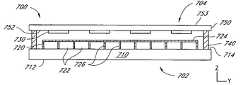
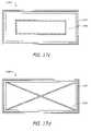
- FIG. 7A and FIG. 7Billustrate an exploded view and cross-section of an embodiment of a packaged electronic device 700 comprising a substrate 710 , an array 720 of interferometric modulators 722 , one or more spacers 730 , a seal 740 , and a backplate 750 .
- the device 700comprises a first side 702 and a second side 704 .
- the substrate 710comprises a first surface 712 and a second surface 714 .
- the interferometric modulator array 720On the second surface 714 of the substrate is formed the interferometric modulator array 720 .
- the backplate 750is secured to the substrate 710 by the seal 740 .
- Disposed between the array 720 and the backplate 750is one or more spacers 730 . Also illustrated in FIG. 7A are x, y, and z axes, and in FIG. 7B , y and z axes referred to in the description herein.
- the substrate 710is any substrate on which an interferometric modulator 722 is formable.
- the device 700displays an image viewable from the first side 702 , and accordingly, the substrate 710 is substantially transparent and/or translucent.
- the substrateis glass, silica, and/or alumina.
- the substrate 710is not substantially transparent and/or translucent, for example, in a device 700 that displays an image viewable from the second side 704 , or in a device 700 that does not display a viewable image.
- the first surface 712 of the substratefurther comprises one or more additional structures, for example, one or more structural, protective, and/or optical films.
- the interferometric modulators 722are of any type.
- the interferometric modulator 722comprises a mechanical layer 724 distal from the substrate 710 and proximal to the backplate 750 .
- the mechanical layer 724is susceptible to physical damage.
- the seal 740secures the backplate 750 to the substrate 710 .
- the term “perimeter support”is also used herein to refer to the seal 740 .
- the seal 740also acts to maintain a predetermined spacing between the backplate 750 and substrate 710 .
- the seal 740 ′does not have a spacing function.
- the sealdoes not produce or outgas a volatile compound, for example, hydrocarbons, acids, amines, and the like.
- the sealis partially or substantially impermeable to liquid water and/or water vapor. In some embodiments, the seal is partially or substantially impermeable to air and/or other gases.
- the sealis rigid. In other embodiments, the seal is elastic or elastomeric. In other embodiments, the seal comprises both rigid, and elastic or elastomeric components. In some embodiments, the seal comprises one or more adhesives compatible with the substrate and/or backplate.
- the adhesive or adhesivesare of suitable any type known in the art. In some embodiments, one or more of the adhesives is pressure sensitive. In some embodiments, one or more of the adhesives is thermally cured. In some embodiments, one or more of the adhesives is UV-cured. In some embodiments, the seal is thermally bonded to the substrate and/or backplate. In some embodiments, the seal is secured to the substrate and/or backplate mechanically. Some embodiments use a combination of methods for securing the seal to the substrate and/or backplate. Some embodiments do not comprise a seal, for example, where the substrate is secured directly to the backplate, for example, by thermal welding.
- the sealcomprises any suitable material, for example, metals, steel, stainless steel, brass, titanium, magnesium, aluminum, copper, tin, lead, zinc, solder, polymer resins, epoxies, polyamides, polyalkenes, polyesters, polysulfones, polystyrene, polyurethanes, polyacrylates, cyanoacrylates, acrylic epoxies, silicones, rubbers, polyisobutylene, neoprene, polyisoprene, styrene-butadiene, parylene, U.V.-curable adhesives, ceramics, glass, silica, alumina, and blends, copolymers, alloys, and/or composites thereof.
- suitable materialfor example, metals, steel, stainless steel, brass, titanium, magnesium, aluminum, copper, tin, lead, zinc, solder, polymer resins, epoxies, polyamides, polyalkenes, polyesters, polysulfone
- the sealfurther comprises a reinforcement, for example, fibers, a mesh, and/or a fabric, for example, glass, metal, carbon, boron, carbon nanotubes, and the like.
- the selected seal materialis partially or substantially water impermeable.
- the sealis a semi-hermetic or hermetic seal.
- the sealis less than about 50 ⁇ m thick, for example, from about 10 ⁇ m to about 30 ⁇ m thick.
- the sealis from about 0.5 mm to about 5 mm wide, for example, from about 1 mm to about 2 mm.
- an embodiment of a method for fabricating the illustrated seal 740 using a UV-curable epoxyis described below.
- the epoxyis applied to the backplate 750 and/or substrate 710 using means known in the art, for example, by printing.
- the type and amount of epoxyis preselected to provide a seal 740 with the desired width, thickness, and moisture permeation properties.
- the backplate 750 and substrate 710are brought together, and the epoxy cured by irradiation with a suitable source of UV radiation.
- a typical epoxyis cured using about 6000 mJ/cm 2 of UV radiation.
- Some embodimentsalso include a post-cure bake at about 80° C.
- the backplate 750is also referred to herein as a “cap” or “backplane.” These terms are not intended to limit the position of the backplate 750 within the device 700 , or the orientation of the device 700 itself.
- the backplate 750protects the array 720 from damage. As discussed above, some embodiments of an interferometric modulator 722 are potentially damaged by physical assaults. Consequently, in some embodiments, the backplate 750 protects the array 720 from contact with foreign objects and/or other components in an apparatus comprising the array 720 , for example. Furthermore, in some embodiments, the backplate 750 protects the array 720 from other environmental conditions, for example, humidity, moisture, dust, changes in ambient pressure, and the like.
- the backplate 750is substantially transparent and/or translucent. In other embodiments, the backplate 750 is not substantially transparent and/or translucent. In some embodiments, the backplate 750 is made from a material that does not produce or outgas a volatile compound, for example, hydrocarbons, acids, amines, and the like. In some embodiments, the backplate 750 is substantially impermeable to liquid water and/or water vapor. In some embodiments, the backplate 750 is substantially impermeable to air and/or other gases.
- Suitable materials for the backplate 750include, for example, metals, steel, stainless steel, brass, titanium, magnesium, aluminum, polymer resins, epoxies, polyamides, polyalkenes, polyesters, polysulfones, polystyrene, polyurethanes, polyacrylates, parylene, ceramics, glass, silica, alumina, and blends, copolymers, alloys, composites, and/or combinations thereof. Examples of suitable composite materials include composite films available from Vitex Systems (San Jose, Calif.).
- the backplate 750further comprises a reinforcement, for example, fibers and/or a fabric, for example, glass, metal, carbon, boron, carbon nanotubes, and the like.
- the backplate 750is substantially rigid. In other embodiments, the backplate 750 is flexible, for example, foil or film. In some embodiments, the backplate 750 is deformed in a predetermined configuration before and/or during assembly of the package structure 700 . As will be discussed in greater detail below, in some embodiments, the backplate 750 is an element in a system for preventing damage to the array 710 .
- the backplate 750comprises an inner surface 752 and an outer surface 753 .
- the inner surface and/or outer surface of the backplatefurther comprise one or more additional structures, for example, a structural, protective, mechanical, and/or optical film or films.
- FIG. 7Billustrates an embodiment of a device 700 ′ in which the inner surface 752 ′ of the backplate is recessed, thereby forming a flange 754 ′ at the perimeter of the backplate 750 ′.
- a backplate with this configurationis referred to as a “recessed cap” herein.
- FIG. 7Dillustrates in cross section an embodiment of a package device 700 ′′ comprising a curved or bowed backplate 750 ′′.
- spacers 730 ′′are disposed near the periphery of an array 720 ′′, which is relatively closer to the backplate 750 ′′, and consequently, more likely to contact the backplate 75 ′′ and sustain damage.
- Other embodimentscomprise a different configuration of one or more spacers. Spacers are discussed in greater detail below.
- the backplate 750 ′′is preformed into the curved configuration.
- the curved shape of the backplate 750 ′′is formed by bending or deforming a substantially flat precursor during assembly of the package device 700 ′′.
- an array 720 ′′ of interferometric modulatorsis formed on a substrate 710 ′′ as described above.
- a seal materialfor example, a UV curable epoxy, is applied to the periphery of a substantially planar backplate 750 ′′, which is wider and/or longer than the substrate 710 ′′.
- the backplate 750 ′′is deformed, for example, by compression, to the desired size, and positioned on the substrate 710 ′′.
- the epoxyis cured, for example, using UV radiation to form the seal 740 ′′.
- FIG. 8Aillustrates a recessed cap 850 in which the inner surface 852 is concave.
- the inner surface 852 and the outer surface 853are not parallel. Consequently, the recessed cap 850 is thinner at the center 858 than at the edge 859 .
- the illustrated embodimentcomprises a peripheral flange 854 , which sets the minimum spacing between the substrate and the inner surface 852 of the recessed cap backplate.
- the peripheral flange 854forms a substantially continuous structure around the periphery of the recessed cap 850 . In other embodiments, the peripheral flange 854 is not continuous.
- the backplate 850comprises reinforcing ribs 856 on the outer surface 853 .
- the reinforcing ribsare on the inner surface 852 or on both surfaces of the backplate.
- the reinforcing structurehas another shape, for example, a grid, or honeycomb. Some embodiments comprise a combination of these features.
- FIG. 8Cillustrates an embodiment of a recessed cap 850 with a concave inner surface 852 and reinforcing ribs 856 on the outer surface 853 .
- Some embodiments of the disclosed backplatesexhibit improved properties, for example, strength, weight, cost, rigidity, transparency, ease of manufacturing, and the like.
- FIG. 8D and FIG. 8Eillustrate in cross section backplates comprising one or more cavities configured to contain a desiccant.
- FIG. 8Dillustrates an embodiment of a backplate 850 comprising a cavity 857 formed on the inner surface 852 of the backplate i.e. between the backplate and the array.
- a desiccant 855is disposed in the cavity 857 .
- FIG. 8Eillustrates an embodiment of a recessed cap backplate 850 comprising two cavities 857 in which desiccant 855 is disposed.
- the desiccant 855substantially does not extend past the inner surface 852 of the backplate. Accordingly, the same spacers discussed below are usable anywhere between the array and backplate.
- the dimensions of the cavities 857are selected according for factors known in the art, for example, the properties of the desiccant, the quantity of desiccant to be used, the amount of moisture to be absorbed, the volume of the device, the mechanical properties of the backplate, and the like. Suitable desiccants and methods for securing a desiccant to a backplate are discussed below. Those skilled in the art will appreciate that in other embodiments, the cavities 857 have a different configuration, for example, length, width, thickness, and/or shape.
- the cavities 857are fabricated by any method known in the art, for example, etching, embossing, stamping, engraving, machining, grinding, milling, sandblasting, molding, slumping, and the like.
- recessesare created by building up the non-recessed portions of the backplate 859 , for example, using an adhesive, welding, fusing, sintering, and the like.
- a slurry of glassis sprayed onto or molded on the backplate and the slurry fused or sintered to form a cavity.
- the seal 740extends between the substrate 710 and backplate 750 .
- the substrate 710 , backplate 750 , and seal 740together substantially completely enclose the array 720 .
- the enclosure 706 formed therefromis substantially impermeable to liquid water, water vapor, and/or particles, for example, dirt or dust.
- the enclosure 706is substantially hermetically and/or semi-hermetically sealed.
- the inner surface 752 of the backplatecontacts the array 720 . In some embodiments, the inner surface 752 does not contact the array 720 . In some embodiments, the gap or headspace between the inner surface 752 of the backplate and the array 720 is at least about 10 ⁇ m. In some preferred embodiments, the gap is from about 30 ⁇ m to about 100 ⁇ m, for example, about 40 ⁇ m, 50 ⁇ m, 60 ⁇ m, 70 ⁇ m, 80 ⁇ m, or 90 ⁇ m. In some embodiments the gap is at greater than 100 ⁇ m, for example 0.5 mm, 1 mm, or greater. In some embodiments, the gap or headspace between the inner surface 752 of the backplate and the array 720 is not constant.
- FIG. 9illustrates an embodiment of the package device 900 comprising a first substrate 910 a , on which a first array 920 a of interferometric modulators 922 a is formed, and a second substrate 910 b , on which a second array 920 b of interferometric modulators 922 b is formed.
- a device with this configurationis also referred to herein as a “double array device.” Such a device may be viewed as one in which the backplate is replaced with a second interferometric modulator array.
- the package device 900is capable of simultaneously displaying a first image on the first array 920 a and a second image on the second array 920 b .
- the package device 900also comprises a seal 940 as described above. Disposed between the first array 920 a and second array 920 b is one or more spacers 930 of any suitable type disclosed herein.
- An embodiment 1000 illustrated in FIG. 10comprises an array 1020 of interferometric modulators formed on a substrate 1010 .
- a recessed cap backplate 1050 and seal 1040 together with the substrate 1010form a cavity or enclosed space 1006 in which is disposed one or more spacers 1030 .
- the backplate 1050comprises one or more units of a desiccant 1055 .
- the desiccantmaintains a reduced humidity within the enclosed space 1006 .
- a package of desiccant 1055is secured to the inner surface 1052 of the backplate, for example, using an adhesive, thermally, and/or mechanically.
- Suitable packaging into which a desiccant is suitably heldare known in the art, including, for example, a container with a mesh surface, a perforated container, a bag made from a permeable fabric or cover stock, and the like.
- the packagingis a sheet of a suitable material secured to the backplate, for example, using a pressure-sensitive adhesive.
- the packageis non-dusting, i.e., resists releasing dust.
- the desiccantis embedded in an inert carrier, for example, a polymer resin, and the assembly secured to the inner surface 1052 .
- the desiccant 1055is directly secured to the inner surface 1052 of the backplate.
- the material from with the backplate 1050is fabricated comprises a desiccant.
- the backplatecomprises a layer of applied desiccant.
- a liquid desiccant or a desiccant dissolved or suspended in a suitable liquidis applied to the backplate 1050 and baked, thereby forming a layer of desiccant on the backplate 1050 .
- a desiccantis mixed with an uncured polymer resin and the mixture applied to the backplate 1050 and cured.
- the desiccantis any suitable desiccant known in the art, for example, metal oxides, calcium oxide, barium oxide, boric anhydride, phosphorus pentoxide, metal sulfates, calcium sulfate, magnesium sulfate, sodium sulfate, metals, sodium, lead/sodium alloy, metal hydrides, sodium borohydride, sodium hydride, lithium aluminum hydride, silica gel, activated alumina, zeolites, molecular sieves, phosphorus, metal salts, magnesium perchlorate, zinc chloride, carbon nanotubes, and combinations thereof.
- metal oxidescalcium oxide, barium oxide, boric anhydride, phosphorus pentoxide, metal sulfates, calcium sulfate, magnesium sulfate, sodium sulfate, metals, sodium, lead/sodium alloy, metal hydrides, sodium borohydride, sodium hydride, lithium aluminum hydride, silica gel, activated a
- the device 700deforms on application of an external force.
- the deformationwill result in relative or differential movement between the array 720 and the backplate 750 .
- forces likely to be encountered in the normal use of the device 700for example, in the construction of the device 700 , in the installation of the device 700 in an apparatus, or in the normal use of the device 700 , are insufficient to cause the array 720 to contact the backplate 750 .
- some components of an interferometric modulator 722for example, the mechanical layer 724 , are susceptible to damage on physical contact. Consequently, in these embodiments, the backplate 750 is unlikely to damage the array 720 and/or interferometric modulators 722 in the array in normal use.
- forces likely to be encountered in normal use of the device 700are sufficient to cause the array 720 to contact the backplate 750 , typically, at or near the center of the backplate 750 and array 720 .
- the relative movement between the array 720 and backplate 750will also increase.
- the length and/or width of a device 700will increase, for example, with increasing size and/or number of the interferometric modulators 722 in the array 720 .
- the increased likelihood of contact between the array 720 and the backplate 750is counteracted by increasing the distance between the array 720 and the backplate 750 .
- the increased likelihood of contact between the array 720 and the backplate 750is counteracted by increasing the rigidity of the device 700 , for example, the substrate 710 , backplate 750 , and/or seal 740 .
- Methods for increasing rigidityare known in the art, and include, for example, increasing the rigidity of a component, modifying the dimensions of a component, changing the shape or profile of a component, adding reinforcement, and the like.
- the increased likelihood of contact between the array 720 and the backplate 750is counteracted by increasing the distance between the array 720 and inner surface 752 of the backplate.
- Some embodiments of the deviceuse a backplate 850 as illustrated in FIG. 8A in which the inner surface 852 is concave, thereby increasing the distance between the center 858 of the backplate and the array 820 .
- increasing the distance between the inner surface of the backplate 752 and the array 720will tend to increase the thickness of the device 700 , particularly if components in the device are also made thicker to increase rigidity. In some applications, a thicker device 700 is undesirable.
- the device 700comprise one or more spacers 730 disposed between the array 720 and the backplate 750 .
- the spacer(s) 730are configured to prevent and/or reduce contact between the array 720 and the backplate 750 when the device 700 is subjected to a deforming force, thereby eliminating and/or reducing damage to the interferometric modulators 722 .
- the backplate 750comprises irregularities or features, for example, reinforcing ribs and/or desiccant packages, as described above.
- the spacers 730prevent an irregularity or feature from contacting the mechanical layer 724 of the array, either directly (e.g., the feature contacting the spacer) or indirectly (e.g., some other part of the backplate contacting the spacer, preventing the feature from contacting the mechanical layer 724 ).
- the surface of the spacer 720 proximal to the array 720is substantially smooth.
- the spacers 730distribute an applied force, thereby reducing the likelihood that the force will damage any particular interferometric modulator 722 .
- a spacer 730distributes an applied force to the posts 726 of the interferometric modulators, thereby protecting the mechanical layer 724 .
- a spacer 730reduces or prevents damage arising from relative lateral or tangential motion between the array 720 and backplate 750 , for example, by sliding and/or rolling.
- the spacer 730comprises one or more low friction surfaces.
- the spacerhas a circular cross section, for example, a sphere or rod.
- the spacer or spacers 730are resilient, thereby absorbing and/or distributing an applied force.
- a spacer 730is designed to concentrate the damage to a small number of interferometric modulators, for example, by using one or more spacers 730 of a particular size and/or shape.
- the array 720comprises redundant pixels such that disabling an isolated pixel is not noticeable to an end user. Accordingly, in these embodiments, the spacer 730 concentrates damage to a single pixel rather than to a group of neighboring pixels, which would be noticeable to the end user.
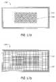
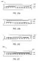
- FIG. 11Ais a top view of the device 1100 illustrating the relative positioning of the spacers and the array.
- the spacerscontact the array, in other embodiments the spacers contact the backplate, and in other embodiments, the spacers contact the array and the backplate.
- the device 1100comprises a plurality of spacers 1130 arranged in a substantially regular pattern over an array 1120 of interferometric modulators formed on a substrate 1110 .
- the spacers 1130are positioned substantially above posts 1126 of the interferometric modulators.
- a spacer 1130is not positioned over every post 1126 .
- the spacers 1130are positioned above the array 1120 . In some embodiments, the spacers 1130 are positioned in the space 110 between the array 1120 and a seal 1140 . In some embodiments, the spacers 1130 are positioned both above the array 1120 and in the space 1110 between the array 1120 and the seal 1140 . Those skilled in the art will understand that other spacings and/or patterns for the spacers 1130 are possible.
- FIG. 11Billustrates a top view of another embodiment of a device 1100 in which the spacers 1130 are arranged substantially randomly over the array 1120 .
- spacers 1130are provided around the center of the array 1120 , but not around the periphery.
- the embodiment of the device 1100 illustrated in FIG. 11Dcomprises a denser arrangement of spacers 1130 around the center of the array 1120 and a sparser arrangement around the periphery.
- the embodiment of the device 1100 illustrated in FIG. 11Ecomprises three concentric zones of spacers 1130 with increasing density towards the center of the array 1120 . Those skilled in the art will understand that other arrangements are possible.
- the spacersare of any suitable size, shape, and material. In some embodiments, all of the spacers are of the same type. Other embodiments comprise spacers of different types, for example, different sizes, shapes, and/or materials.
- the particular dimensions for a spacerwill depend on factors known in the art including the material from which the spacer is made, the headspace between the array and the backplate, the intended application for the display package, and the like.
- the thickness of the spaceris similar to the headspace between the array and the backplate. In other embodiments, the thickness of the spacer is less than the headspace between the array and the backplate. The dimensions of the headspace are discussed above.
- Suitable materials for the spacersinclude rigid materials and/or elastomeric materials.
- the spacerscomprise a material capable of absorbing at least a portion of a force applied thereto, for example, by deformation.
- the spaceris elastic and returns to substantially the original shape after the deforming force is removed. In other embodiments, the spacer permanently deforms in absorbing the force applied thereto.
- the spaceris a composite, for example, comprising a core of one material and a coating of another.
- the spacercomprises a core of a rigid material, for example a metal, and a coating of an elastomeric material, for example, a polymer resin.
- the spacersare transparent or translucent.
- the spacersare electrically conductive.
- the spacerscomprise a desiccant of any type known in the art, for example, metal oxides, calcium oxide, barium oxide, boric anhydride, phosphorus pentoxide, metal sulfates, calcium sulfate, magnesium sulfate, sodium sulfate, metals, sodium, lead/sodium alloy, metal hydrides, sodium borohydride, sodium hydride, lithium aluminum hydride, silica gel, activated alumina, zeolites, molecular sieves, phosphorus, metal salts, magnesium perchlorate, zinc chloride, carbon nanotubes, and combinations thereof.
- the spacersubstantially comprises a desiccant.
- the spacercomprises a composite in which the desiccant is a component. In some embodiments, the desiccant is distributed throughout the composite. In other embodiments, the desiccant is concentrated in one portion of the spacer, for example in a core.
- the other component or components in the compositeare any suitable material, for example, the materials disclosed above as suitable for a spacer.
- another materialfor example, a coating over the desiccant, is a material that is permeable to water and/or water vapor, thereby facilitating the absorption of water by the desiccant.
- the coatingcomprises one or more openings, for example, made by abrading the coating or through the manufacturing process of the spacer, to permit contact between the desiccant in the core and the ambient atmosphere.
- Spacersare manufactured using methods known in the art, which will depend upon factors know in the art, including the material or materials from with the spacers are made, the size and shape of the spacers, the tolerances for the spacers.
- the spacersare applied as a fluid, for example, a liquid, a gel, and/or a paste, which is then cured to form the spacers.
- suitable fluid materialsinclude, for example, adhesives and photoresists.
- curing conditionsdepend on the particular material, and include thermal curing, photocuring, UV curing, and/or radiation curing.
- the spacersare pre-manufactured. Embodiments of pre-manufactured spacers are illustrated in FIG. 12A-FIG . 12 T. Those skilled in the art will understand that the illustrated shapes are exemplary and that other shapes are possible. For example, in some embodiments, the spacers are irregularly shaped. In some embodiments, the spacers are substantially solid. In other embodiments, the spacers comprise one or more voids. For example, in some embodiments, the spacer comprises one or more hollow regions. In some embodiments, the spacer comprises a plurality of voids, for example, an open-cell or closed-cell foam. Spherical and rod-shaped spacers illustrated in FIG. 12D and FIG.
- glass rod-shaped spacersare commercially available from Nippon Electric Glass Co. (Otsu, Shiga, Japan) in diameters of from about 1.5 ⁇ m to about 60 ⁇ m.
- Plastic spherical spacersare commercially available, for example, from Sekisui Chemical Co. (Osaka, Japan) in diameters of from about 5 ⁇ m to about 350 ⁇ m.
- Some embodimentsuse such spacers for reasons of availability, uniformity, and/or cost.
- Other shapesfor example, squares and circles, are also readily manufactured, and are used in other embodiments.
- the spacercomprises one or more projections and/or indentations, for example, as illustrated in FIG. 12N-FIG . 12 T.
- the projections and/or indentationsengage a structure or feature on the array and/or backplate, as discussed in greater detail below.
- the projections and/or indentationsare designed to absorb at least some of the force applied to the device.
- some embodimentscomprise springs, as illustrated in FIG. 12P-FIG . 12 S.
- Some embodimentscomprise projections, as illustrated in FIG. 12N , FIG. 12O , and FIG. 12T , which are discussed in greater detail below.
- the embodiment illustrated in FIG. 12Tcomprises both projections 1232 and indentations 1234 .
- the spacer 1330spans at least two posts 1326 of the array 1320 of interferometric modulators.
- the shortest diameter D of the spacer 1330is at least about twice the spacing d between the posts 1326 , which ensures that the spacer always spans at least two posts 1326 .
- the spacing dis from about 30 ⁇ m to about 80 ⁇ m, for example, about 30 ⁇ m, 40 ⁇ m, 50 ⁇ m, 60 ⁇ m, or 30 ⁇ m. In other embodiments, the spacing d is larger, for example, up to 1 mm, or up to 5 mm.
- the array 1320comprises interferometric modulators 1322 with different dimensions, for example, widths, and consequently, the spacing between posts 1326 for adjacent interferometric modulators 1322 is not uniform. Consequently in some embodiments, the dimension D is at least the largest distance between the outer posts 1326 of adjacent interferometric modulators 1322 .
- FIG. 13BOne embodiment of such an arrangement is illustrated in FIG. 13B , in which the posts 1326 ′ have a different design than those illustrated in FIG. 13A and the spacers 1330 ′ are disk-shaped.
- the spacer 1430is at least a large as an interferometric modulator 1422 , and consequently, is positioned at least over one post 1426 .
- the spacer 1430is a perforated square. Interferometric modulator sizes are discussed above.
- each spacer 1530is substantially centered over a post 1526 .
- a least a portion of each spacer 1530is positioned over a post 1526 .
- no portion of each spacer 1530is positioned over a post 1526 .
- Other embodiments, not illustrated,include any combination of these arrangements.
- the embodiment of the device 1600 illustrated in FIG. 16comprises spacers 1630 of different sizes positioned substantially over the array 1620 .
- FIG. 17Aillustrates an embodiment of a device 1700 that comprises a spacer 1730 in the form of a mesh positioned over the center portion of the array 1720 .
- FIG. 17Billustrates an embodiment of a device 1700 that comprises a mesh spacer 1730 that is denser around the center than around the peripheral portion.
- FIG. 17Cillustrates an embodiment of a device 1700 in which the spacer 1730 is roughly an open rectangle substantially centered over the array 1720 .
- FIG. 17Dillustrates an embodiment of a device 1700 in which the spacer 1730 is substantially defined by the diagonals of the array 1720 .
- the spaceris thicker in one or more regions and thinner in one or more regions.
- the spaceris thicker in the central region and thinner around the periphery.
- the spacer 1730comprises a desiccant, as discussed above.
- the spacer 1730comprises a core of a desiccant surrounded by an outer layer, for example, a polymer resin.
- a desiccantis embedded into the spacer material.
- An embodiment 1800 illustrated in FIG. 18Acomprises a spacer 1830 in the form of a film disposed between the array 1820 and the backplate 1850 .
- the spacer 1830extends beyond the array 1820 .
- the spacer 1830does not extend beyond the array 1820 .
- the spacer 1830is substantially coextensive with the array 1820 .
- the spacer 1830does not cover the entire array 1820 .
- the filmis substantially a flat film. In some embodiments, the film is from about 5 ⁇ m to about 50 ⁇ m thick, for example, from about 10 ⁇ m to about 20 ⁇ m thick. In other embodiments, the film is thicker. In some embodiments, the film is sufficiently thick to substantially fill the space between the array and backplate. In some embodiments, the film comprises a resilient material, for example, a foam. In some embodiments, the foam has a covering, for example, a non-permeable polymer, which in some embodiments, comprises perforations. In other embodiments, the film has a different shape. FIG.
- the film spacer 1830 ′in the form of a film with a non-planar cross section, for example, corrugated or an “egg-crate” shape, which absorbs at least some of the deforming force when compressed between the array 1820 ′ and the backplate 1850 ′.
- a non-planar filmis thicker than the corresponding planar film.
- the film spacercomprises areas of varying properties, for example, thickness, compositions (e.g., composites), projections, indentations, and the like.
- one or both faces of the filmfurther comprises additional spacers as described above, for example, the spacers illustrated in FIG. 12A-FIG . 12 T.
- the film and spacersare formed as an integrated unit. In other embodiments the spacers and film are fabricated separately and joined in a separate step.
- the filmis perforated.
- some embodiments of the spacers illustrated in FIG. 17A and FIG. 17Bare perforated films.
- FIG. 18Cillustrates an embodiment in which the spacer 1830 ′′ is a sealed bag enclosing a volume of gas disposed between the array 1820 ′′ and the backplate 1850 ′′.
- the particular film selected for an applicationwill depend on factors including the thickness of the film, its mechanical properties, its shape and configuration, the headspace between the array and backplate, and the anticipated use of the display package.
- the filmcomprises a desiccant. In some embodiments, the film is a desiccant. In other embodiments, the film, for example, a polymer resin film, is impregnated with a desiccant. In still other embodiments, the film comprises a thin layer of desiccant that is encapsulated, for example, using a polymer resin.
- Some embodimentscomprise a planar film spacer in contact with the array or a portion thereof in order to distribute forces over a larger area.
- one or more other spacers as disclosed hereinare positioned between the film and the backplate, and/or between the film and the array, for example any of the spacers described above.
- FIG. 19illustrates an embodiment 1900 comprising a plurality of film spacers 1930 disposed between the array 1920 and the backplate 1950 .
- the film spacersare as described above.
- Some embodimentscomprise a combination of a planar film spacer and a non-planar film spacer, for example, with the planar film spacer contacting the array 1920 as described above.
- Some embodimentscomprise at least two non-planar film spacers arranged such that the spacers do not nest, for example, a pair of corrugated films arranged with the corrugations at right angles.
- Some embodimentscomprise at least two non-planar film spacers with a planar film spacer disposed in-between thereby preventing the non-planar spacers from nesting.
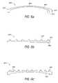
- the spacer or some portion thereofhas a shape designed to provide a graded response to an applied force, for example, a spacer or portion thereof with a triangular cross section.
- An example of a portion of a spaceris provided FIG. 12T as projection 1232 .
- a triangular portion of a spaceris illustrated in FIG. 20A .
- the triangular portionis relatively susceptible to small deformations, as illustrated in FIG. 20B , but becomes increasingly difficult to deform as illustrated in FIG. 20C and FIG. 20D .
- FIG. 20Eillustrates another embodiment in which the spacer 2032 has two regions, each which has a different response to an applied force: a thinner upper portion 2032 a and a thicker lower portion 2034 b .
- the spacer 2030 ′also has two response regions, an upper region 2032 ′ that is has relatively more void space, and a lower region 2034 ′ that has relatively less void space.
- spacercomprises a composite that provides a graded response.
- one or more of the spacersis secured to the array. In other embodiments, one or more of the spacers is secured to the backplate. In other embodiments, one or more of the spacers is secured to both the array and the backplate. In other embodiments, a first set of one or more spacers is secured to the array, and a second set of one or more spacers is secured to the backplate. In other embodiments, one or more of the spacers is not secured to either the array or the backplate. In embodiments in which a spacer is secured to the array and or backplate, the spacer is secured using any method known in the art, for example, using an adhesive, mechanically, and/or by welding.
- one or more adhesivesis applied to the array and/or backplate using any method known in the art, for example, lithographically, inkjet printing, contact printing, and the like.
- a spacer or spacersis then applied to the adhesive.
- the adhesiveis applied to the spacer, which is then applied to the array and/or backplate, for example, by spraying, rolling, individual application, and the like.
- the spacersare suspended in a liquid comprising the adhesive. The suspension of spacers is applied to the array and the liquid removed, for example, by evaporation.
- suitable liquidsinclude lower alcohols, for example, methanol, ethanol, and isopropanol, as well as other volatile liquids, for example, acetone, methyl t-butyl ether, and ethyl acetate.
- spacersare applied to a film, which is then applied to the array and/or backplate.
- the spaceris integral to the array or backplate, as described in greater detail below. Spacers are secured to the backplate using substantially similar methods.
- one or more spacersare not secured to the array or the backplate.
- the spacersare simply positioned on the array and/or backplate in the assembly of the package device.
- the spacersare conveniently positioned by suspending them in a fluid carrier and applying the suspended spacers to the array and/or backplate, for example, by spraying and/or spin coating.
- the fluid carrieris a liquid that is easily removed, for example, under vacuum and/or by heating.
- suitable liquidsinclude lower alcohols (e.g., methanol, ethanol, isopropanol), hydrocarbons (e.g., propane, butane, pentane), halogenated compounds (e.g., fluorocarbons, chlorofluorocarbons, hydrochlorofluorocarbons, chlorocarbons, hydrochlorocarons), ethers (e.g., methyl tert-butyl ether, diethyl ether, tetrahydrofuran), esters (e.g., ethyl acetate), ketones (e.g., acetone), and combinations thereof.
- the fluidis a gas, for example, air or nitrogen.
- the spacerstend to remain in position after the solvent is removed, even absent an added adhesive.
- the spacersare applied substantially only over the array, for example, by masking the area on which the seal is formed during the application of the spacers. In other embodiments, the spacers are applied over the array as well as other portions of the device, for example, over the area on which the seal is formed. In some of these embodiments, the spacers also define the thickness of the seal, thereby providing a uniform seal thickness. For example, disposing 20- ⁇ m spacers within the seal and contacting the substrate and backplate with the spacers provides a seal thickness of 20 ⁇ m.
- one or more of the spacers 2130extends between the array 2120 and backplate 2150 .
- the spacer 2130 ′contacts the array 2120 ′, but does not contact the backplate 2150 ′.
- the spacer 2130 ′′contacts the backplate 2150 ′′, but does not contact the array 2120 ′′.
- FIG. 22Ais similar to the device illustrated in FIG. 6C .
- the spacers 2230are integrated with the array 2220 interferometric modulators.
- the spacers 2230are formed over the posts 2226 of the interferometric modulators 2222 .
- the process for forming the spacers 2230is a thin-film process, and is integrated with the process for forming the interferometric modulators 2222 , for example, as disclosed above and in U.S. Pat. No. 5,835,255.
- a spacer materialis deposited on the mechanical layer 2224 prior to the removal of the sacrificial material (not illustrated) in the process for manufacturing the interferometric modulators 2222 .
- the spacers 2230are patterned and etched from the spacer material using methods known in the art. Those skilled in the art will understand that the particular method will depend on factors including the particular spacer material used, the other materials used in the manufacture of the interferometric modulators 2222 , the geometries of the interferometric modulators 2222 , and the like.
- the formation of the spacers 2230is integrated in the process flow for forming interferometric modulators, for example, the process disclosed in U.S. Pat. No. 5,835,255.
- a layer (not shown) of the spacer materialis deposited on the mechanical layer 2224 before removal of a sacrificial material (not shown) occupying the cavity between the mirrors.
- the spacer layeris then etched to form the individual spacers 2230 .
- the spacer layeris patterned and etched so that a passage allowing gas communication to each cavity in an array 2220 of interferometric modulators is formed. The cavity is then formed by removing the sacrificial material through the passage.
- the integrated spacersare fabricated from a solid material with good shape retention that is not easily compressed.
- the materialis selected from the group consisting of metals, oxides, nitrides, photoresists, other organic materials, spin-on glass, and combinations thereof.
- the spacersare electrically conductive. Those skilled in the art will understand that similar processes are useful in fabricating integrated spacers on the inner surface of the backplate.
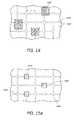
- the array 2220 ′comprises interferometric modulators 2222 ′ of different heights.
- the first spacers 2230 ′compensate for the height differences, thereby providing a uniform platform supporting second spacers 2260 ′ of any type disclosed above.
- the second spacers 2260 ′are secured to the first spacers.
- the second spacers 2260 ′are not secured to the first spacers.
- the second spacers 2260 ′′comprises indentations 2234 ′′ that engage the first spacers 2230 ′′.
- FIG. 23is a flowchart illustrating a method for manufacturing a packaged electronic device with reference to the structure illustrated in FIG. 7A and FIG. 7B .
- a substrate 710 on which an interferometric modulator 722 has been formedis obtained.
- the interferometric modulator 722is part of an array 720 of interferometric modulators 722 .
- a backplate 750is obtained.
- one or more spacers 730are disposed between the interferometric modulator 722 and the backplate 750 .
- a seal 740is formed between the substrate 710 and the backplate 750 .
- the product of the manufacturing processis a panel comprising a plurality of package displays.
- the individual package displaysare then cut from the panel.
- a plurality of interferometric modulator arraysis formed on a single substrate (mother glass), as discussed above.
- a sheet comprising a plurality of backplates (typically equal in number to the interferometric modulator arrays) dimensioned and spaced to match the interferometric arraysis obtained. Spacers are disposed between the substrate and backplate as discussed above. Seals are formed between each array and backplate as discussed above, thereby forming a panel comprising a plurality of interferometric modulator arrays.
- the individual package displaysare cut from the panel using any method known in the art, for example, by scribing.
- FIG. 24is a flowchart illustrating a method for protecting an electronic device with reference to the structure illustrated in FIG. 7A and FIG. 7B .
- a devicecomprising an interferometric modulator 722 formed on a substrate 710 and a backplate 750 is obtained.
- one or more spacersare disposed between the interferometric modulator 722 and the backplate 750 .
- the isopropanolis removed by heating at 100° C. for 5 seconds.
- a bead of a UV curing epoxy(H5516, Nagase, Tokyo, Japan) is applied to the peripheries of the recessed cap backplates and the sheet aligned over the substrate. Pressure is applied to the sheet to provide a layer of epoxy with a 15 ⁇ m average thickness.
- the epoxyis cured by irradiating at 6000 mJ/cm 2 350 nm (about 2 minutes), then baking at 80° C. for 30 min. Six interferometric modulator packages are cut from the resulting panel.
Landscapes
- Physics & Mathematics (AREA)
- Engineering & Computer Science (AREA)
- Microelectronics & Electronic Packaging (AREA)
- General Physics & Mathematics (AREA)
- Optics & Photonics (AREA)
- Computer Hardware Design (AREA)
- General Health & Medical Sciences (AREA)
- Spectroscopy & Molecular Physics (AREA)
- Toxicology (AREA)
- Health & Medical Sciences (AREA)
- Nonlinear Science (AREA)
- Mechanical Light Control Or Optical Switches (AREA)
- Devices For Indicating Variable Information By Combining Individual Elements (AREA)
- Control Of Indicators Other Than Cathode Ray Tubes (AREA)
- Micromachines (AREA)
Abstract
Description
Claims (33)
Priority Applications (16)
| Application Number | Priority Date | Filing Date | Title |
|---|---|---|---|
| US11/108,026US7573547B2 (en) | 2004-09-27 | 2005-04-15 | System and method for protecting micro-structure of display array using spacers in gap within display device |
| AU2005209661AAU2005209661A1 (en) | 2004-09-27 | 2005-09-12 | System and method for protecting micro-structure of display array using spacers in gap within display device |
| ES05255641TES2416360T3 (en) | 2004-09-27 | 2005-09-14 | System and procedure to protect the microstructure of a display matrix using spacers in a strike within the display device |
| EP05255641.2AEP1640322B1 (en) | 2004-09-27 | 2005-09-14 | System and method for protecting micro-structure of display array using spacers in gap within display device |
| MYPI20054363AMY140654A (en) | 2004-09-27 | 2005-09-16 | System and method for protecting micro-structure of display array using spacers in gap within display device |
| SG200506061ASG121159A1 (en) | 2004-09-27 | 2005-09-21 | System and method for protecting micro-structure of display array using spacers in gap within display device |
| CA002520358ACA2520358A1 (en) | 2004-09-27 | 2005-09-21 | System and method for protecting micro-structure of display array using spacers in gap within display device |
| JP2005276442AJP4674808B2 (en) | 2004-09-27 | 2005-09-22 | Display device and method of manufacturing display device |
| TW102111753ATWI438524B (en) | 2004-09-27 | 2005-09-22 | System and method for protecting micro-structure of display array using spacers in gap within display device |
| TW094132853ATWI438522B (en) | 2004-09-27 | 2005-09-22 | System and method for protecting micro-structure of display array using spacers in gap within display device |
| CN2011103168706ACN102354049A (en) | 2004-09-27 | 2005-09-23 | System and method for protecting micro-structure of display array using spacers in gap within display device |
| MXPA05010256AMXPA05010256A (en) | 2004-09-27 | 2005-09-23 | System and method for protecting micro-structure of display array using spacers in gap within display device. |
| BRPI0503904-5ABRPI0503904A (en) | 2004-09-27 | 2005-09-27 | system and method for protecting display matrix microstructure using interval spacers within the display device |
| KR1020050089839AKR101287981B1 (en) | 2004-09-27 | 2005-09-27 | System and method for protecting micro-structure of display array using spacers in gap within display device |
| JP2009223128AJP5237233B2 (en) | 2004-09-27 | 2009-09-28 | System and method for protecting the microstructure of a display array by using spacers in the gaps in the display device |
| JP2012279879AJP2013117726A (en) | 2004-09-27 | 2012-12-21 | System and method for protecting micro-structure of display array using spacers in gap within display device |
Applications Claiming Priority (3)
| Application Number | Priority Date | Filing Date | Title |
|---|---|---|---|
| US61368204P | 2004-09-27 | 2004-09-27 | |
| US61340604P | 2004-09-27 | 2004-09-27 | |
| US11/108,026US7573547B2 (en) | 2004-09-27 | 2005-04-15 | System and method for protecting micro-structure of display array using spacers in gap within display device |
Publications (2)
| Publication Number | Publication Date |
|---|---|
| US20060077147A1 US20060077147A1 (en) | 2006-04-13 |
| US7573547B2true US7573547B2 (en) | 2009-08-11 |
Family
ID=35207587
Family Applications (1)
| Application Number | Title | Priority Date | Filing Date |
|---|---|---|---|
| US11/108,026Expired - Fee RelatedUS7573547B2 (en) | 2004-09-27 | 2005-04-15 | System and method for protecting micro-structure of display array using spacers in gap within display device |
Country Status (13)
| Country | Link |
|---|---|
| US (1) | US7573547B2 (en) |
| EP (1) | EP1640322B1 (en) |
| JP (3) | JP4674808B2 (en) |
| KR (1) | KR101287981B1 (en) |
| CN (1) | CN102354049A (en) |
| AU (1) | AU2005209661A1 (en) |
| BR (1) | BRPI0503904A (en) |
| CA (1) | CA2520358A1 (en) |
| ES (1) | ES2416360T3 (en) |
| MX (1) | MXPA05010256A (en) |
| MY (1) | MY140654A (en) |
| SG (1) | SG121159A1 (en) |
| TW (2) | TWI438522B (en) |
Cited By (38)
| Publication number | Priority date | Publication date | Assignee | Title |
|---|---|---|---|---|
| US20070268581A1 (en)* | 2006-05-17 | 2007-11-22 | Qualcomm Incorporated | Desiccant in a mems device |
| US20080232615A1 (en)* | 2007-03-21 | 2008-09-25 | Goer Tek Inc. | Condenser microphone chip |
| US20090059342A1 (en)* | 2004-09-27 | 2009-03-05 | Idc, Llc | Method and device for packaging a substrate |
| US20110012219A1 (en)* | 2007-09-28 | 2011-01-20 | Qualcomm Mems Technologies, Inc. | Optimization of desiccant usage in a mems package |
| US20110042552A1 (en)* | 2009-08-19 | 2011-02-24 | Furuya Shogo | Solid-state imaging device and method of manufacturing the same |
| US20110157679A1 (en)* | 2008-08-04 | 2011-06-30 | Pixtronix, Inc. | Methods for manufacturing cold seal fluid-filled display apparatus |
| US20110235156A1 (en)* | 2010-03-26 | 2011-09-29 | Qualcomm Mems Technologies, Inc. | Methods and devices for pressure detection |
| WO2011130715A2 (en) | 2010-04-16 | 2011-10-20 | Flex Lighting Ii, Llc | Illumination device comprising a film-based lightguide |
| WO2011130718A2 (en) | 2010-04-16 | 2011-10-20 | Flex Lighting Ii, Llc | Front illumination device comprising a film-based lightguide |
| US20120026577A1 (en)* | 2010-07-28 | 2012-02-02 | E Ink Holdings Inc. | Display device and manufacturing method thereof |
| US8284475B2 (en) | 2007-05-11 | 2012-10-09 | Qualcomm Mems Technologies, Inc. | Methods of fabricating MEMS with spacers between plates and devices formed by same |
| US8379392B2 (en) | 2009-10-23 | 2013-02-19 | Qualcomm Mems Technologies, Inc. | Light-based sealing and device packaging |
| US8482496B2 (en) | 2006-01-06 | 2013-07-09 | Pixtronix, Inc. | Circuits for controlling MEMS display apparatus on a transparent substrate |
| US8519945B2 (en) | 2006-01-06 | 2013-08-27 | Pixtronix, Inc. | Circuits for controlling display apparatus |
| US8519923B2 (en) | 2005-02-23 | 2013-08-27 | Pixtronix, Inc. | Display methods and apparatus |
| US8526096B2 (en) | 2006-02-23 | 2013-09-03 | Pixtronix, Inc. | Mechanical light modulators with stressed beams |
| US8599463B2 (en) | 2008-10-27 | 2013-12-03 | Pixtronix, Inc. | MEMS anchors |
| US20130321749A1 (en)* | 2012-06-01 | 2013-12-05 | Shenzhen China Star Optoelectronics Technology Co., Ltd. | Liquid Crystal Display Device |
| US20140063501A1 (en)* | 2012-08-30 | 2014-03-06 | Seiko Epson Corporation | Variable wavelength interference filter, optical module, electronic apparatus, and method of manufacturing variable wavelength interference filter |
| US8693084B2 (en) | 2008-03-07 | 2014-04-08 | Qualcomm Mems Technologies, Inc. | Interferometric modulator in transmission mode |
| US20140192060A1 (en)* | 2013-01-08 | 2014-07-10 | Qualcomm Mems Technologies, Inc. | Controlling movable layer shape for electromechanical systems devices |
| US20140264693A1 (en)* | 2013-03-12 | 2014-09-18 | Optiz, Inc. | Cover-Free Sensor Module And Method Of Making Same |
| US8941909B2 (en) | 2011-05-17 | 2015-01-27 | Pixtronix, Inc. | Display device |
| US9057872B2 (en) | 2010-08-31 | 2015-06-16 | Qualcomm Mems Technologies, Inc. | Dielectric enhanced mirror for IMOD display |
| US9082353B2 (en) | 2010-01-05 | 2015-07-14 | Pixtronix, Inc. | Circuits for controlling display apparatus |
| US9087486B2 (en) | 2005-02-23 | 2015-07-21 | Pixtronix, Inc. | Circuits for controlling display apparatus |
| US20150253612A1 (en)* | 2012-09-28 | 2015-09-10 | Panasonic Intellectual Property Management Co., Ltd. | Display device |
| US9134552B2 (en) | 2013-03-13 | 2015-09-15 | Pixtronix, Inc. | Display apparatus with narrow gap electrostatic actuators |
| US9135868B2 (en) | 2005-02-23 | 2015-09-15 | Pixtronix, Inc. | Direct-view MEMS display devices and methods for generating images thereon |
| US9158106B2 (en) | 2005-02-23 | 2015-10-13 | Pixtronix, Inc. | Display methods and apparatus |
| US9176318B2 (en) | 2007-05-18 | 2015-11-03 | Pixtronix, Inc. | Methods for manufacturing fluid-filled MEMS displays |
| US9229222B2 (en) | 2005-02-23 | 2016-01-05 | Pixtronix, Inc. | Alignment methods in fluid-filled MEMS displays |
| US9261694B2 (en) | 2005-02-23 | 2016-02-16 | Pixtronix, Inc. | Display apparatus and methods for manufacture thereof |
| US9336732B2 (en) | 2005-02-23 | 2016-05-10 | Pixtronix, Inc. | Circuits for controlling display apparatus |
| US9500853B2 (en) | 2005-02-23 | 2016-11-22 | Snaptrack, Inc. | MEMS-based display apparatus |
| US9543347B2 (en) | 2015-02-24 | 2017-01-10 | Optiz, Inc. | Stress released image sensor package structure and method |
| US9575723B2 (en) | 2013-03-14 | 2017-02-21 | International Business Machines Corporation | Software interface for a specialized hardware device |
| US9588333B2 (en) | 2013-01-07 | 2017-03-07 | Seiko Epson Corporation | Wavelength tunable interference filter, method for manufacturing wavelength tunable interference filter, optical module, and electronic apparatus |
Families Citing this family (68)
| Publication number | Priority date | Publication date | Assignee | Title |
|---|---|---|---|---|
| US6794119B2 (en)* | 2002-02-12 | 2004-09-21 | Iridigm Display Corporation | Method for fabricating a structure for a microelectromechanical systems (MEMS) device |
| US7573547B2 (en)* | 2004-09-27 | 2009-08-11 | Idc, Llc | System and method for protecting micro-structure of display array using spacers in gap within display device |
| US7626581B2 (en)* | 2004-09-27 | 2009-12-01 | Idc, Llc | Device and method for display memory using manipulation of mechanical response |
| US7405924B2 (en)* | 2004-09-27 | 2008-07-29 | Idc, Llc | System and method for protecting microelectromechanical systems array using structurally reinforced back-plate |
| US8194056B2 (en)* | 2006-02-09 | 2012-06-05 | Qualcomm Mems Technologies Inc. | Method and system for writing data to MEMS display elements |
| WO2007120887A2 (en)* | 2006-04-13 | 2007-10-25 | Qualcomm Mems Technologies, Inc | Packaging a mems device using a frame |
| KR101292765B1 (en)* | 2006-10-31 | 2013-08-02 | 삼성디스플레이 주식회사 | Display Apparatus and Method of Fabricating the Same |
| US7816164B2 (en)* | 2006-12-01 | 2010-10-19 | Qualcomm Mems Technologies, Inc. | MEMS processing |
| US20090034223A1 (en)* | 2007-07-31 | 2009-02-05 | Doczy Paul J | Electronic device housing assembly |
| JP2009086276A (en)* | 2007-09-28 | 2009-04-23 | Hitachi Ltd | Image display device and support structure thereof |
| EP2043415B1 (en) | 2007-09-28 | 2013-08-21 | Hitachi, Ltd. | Image displaying apparatus |
| CN101458604B (en)* | 2007-12-12 | 2012-03-28 | 清华大学 | Touch screen and display device |
| CN101458609B (en)* | 2007-12-14 | 2011-11-09 | 清华大学 | Touch screen and display device |
| CN101458597B (en)* | 2007-12-14 | 2011-06-08 | 清华大学 | Touch screen, method for producing the touch screen, and display device using the touch screen |
| CN101620454A (en)* | 2008-07-04 | 2010-01-06 | 清华大学 | Potable computer |
| CN101458608B (en)* | 2007-12-14 | 2011-09-28 | 清华大学 | Touch screen preparation method |
| CN101458594B (en)* | 2007-12-12 | 2012-07-18 | 清华大学 | Touch screen and display device |
| CN101458603B (en)* | 2007-12-12 | 2011-06-08 | 北京富纳特创新科技有限公司 | Touch screen and display device |
| CN101470559B (en)* | 2007-12-27 | 2012-11-21 | 清华大学 | Touch screen and display equipment |
| CN101458599B (en)* | 2007-12-14 | 2011-06-08 | 清华大学 | Touch screen, method for producing the touch screen, and display device using the touch screen |
| CN101676832B (en)* | 2008-09-19 | 2012-03-28 | 清华大学 | Desktop PC |
| CN101458598B (en)* | 2007-12-14 | 2011-06-08 | 清华大学 | Touch screen and display device |
| CN101470560B (en)* | 2007-12-27 | 2012-01-25 | 清华大学 | Touch screen and display equipment |
| CN101458595B (en)* | 2007-12-12 | 2011-06-08 | 清华大学 | Touch screen and display device |
| CN101458593B (en)* | 2007-12-12 | 2012-03-14 | 清华大学 | Touch screen and display device |
| CN101656769B (en)* | 2008-08-22 | 2012-10-10 | 清华大学 | Mobile telephone |
| CN101419519B (en)* | 2007-10-23 | 2012-06-20 | 清华大学 | Touch panel |
| CN101458605B (en)* | 2007-12-12 | 2011-03-30 | 鸿富锦精密工业(深圳)有限公司 | Touch screen and display device |
| CN101458606B (en)* | 2007-12-12 | 2012-06-20 | 清华大学 | Touch screen, method for producing the touch screen, and display device using the touch screen |
| CN101458600B (en)* | 2007-12-14 | 2011-11-30 | 清华大学 | Touch screen and display device |
| CN101464763B (en)* | 2007-12-21 | 2010-09-29 | 清华大学 | Manufacturing method of touch screen |
| CN101470566B (en)* | 2007-12-27 | 2011-06-08 | 清华大学 | Touch control device |
| CN101419518B (en)* | 2007-10-23 | 2012-06-20 | 清华大学 | Touch panel |
| CN101470558B (en)* | 2007-12-27 | 2012-11-21 | 清华大学 | Touch screen and display equipment |
| CN101458596B (en)* | 2007-12-12 | 2011-06-08 | 北京富纳特创新科技有限公司 | Touch screen and display device |
| CN101655720B (en)* | 2008-08-22 | 2012-07-18 | 清华大学 | Personal digital assistant |
| CN101458602B (en)* | 2007-12-12 | 2011-12-21 | 清华大学 | Touch screen and display device |
| CN101458975B (en)* | 2007-12-12 | 2012-05-16 | 清华大学 | Electronic element |
| CN101464757A (en)* | 2007-12-21 | 2009-06-24 | 清华大学 | Touch screen and display equipment |
| CN101458607B (en)* | 2007-12-14 | 2010-12-29 | 清华大学 | Touch screen and display device |
| CN101458601B (en)* | 2007-12-14 | 2012-03-14 | 清华大学 | Touch screen and display device |
| CN101464766B (en)* | 2007-12-21 | 2011-11-30 | 清华大学 | Touch screen and display equipment |
| CN101464765B (en)* | 2007-12-21 | 2011-01-05 | 鸿富锦精密工业(深圳)有限公司 | Touch screen and display equipment |
| US8574393B2 (en)* | 2007-12-21 | 2013-11-05 | Tsinghua University | Method for making touch panel |
| CN101470565B (en)* | 2007-12-27 | 2011-08-24 | 清华大学 | Touch screen and display device |
| CN101464764B (en)* | 2007-12-21 | 2012-07-18 | 清华大学 | Touch screen and display equipment |
| US7746539B2 (en)* | 2008-06-25 | 2010-06-29 | Qualcomm Mems Technologies, Inc. | Method for packing a display device and the device obtained thereof |
| US20090323170A1 (en)* | 2008-06-30 | 2009-12-31 | Qualcomm Mems Technologies, Inc. | Groove on cover plate or substrate |
| US8237677B2 (en)* | 2008-07-04 | 2012-08-07 | Tsinghua University | Liquid crystal display screen |
| US8390580B2 (en)* | 2008-07-09 | 2013-03-05 | Tsinghua University | Touch panel, liquid crystal display screen using the same, and methods for making the touch panel and the liquid crystal display screen |
| US20100020382A1 (en)* | 2008-07-22 | 2010-01-28 | Qualcomm Mems Technologies, Inc. | Spacer for mems device |
| US8410690B2 (en)* | 2009-02-13 | 2013-04-02 | Qualcomm Mems Technologies, Inc. | Display device with desiccant |
| CN101924816B (en)* | 2009-06-12 | 2013-03-20 | 清华大学 | Flexible mobile phone |
| NO333724B1 (en)* | 2009-08-14 | 2013-09-02 | Sintef | A micromechanical series with optically reflective surfaces |
| JP5310529B2 (en)* | 2009-12-22 | 2013-10-09 | 株式会社豊田中央研究所 | Oscillator for plate member |
| US20120134008A1 (en)* | 2010-11-30 | 2012-05-31 | Ion Bita | Electromechanical interferometric modulator device |
| US20120235959A1 (en)* | 2011-03-15 | 2012-09-20 | Qualcomm Mems Technologies, Inc. | Seal anchor structures |
| US20120327092A1 (en)* | 2011-06-21 | 2012-12-27 | Qualcomm Mems Technologies, Inc. | Planarized spacer for cover plate over electromechanical systems device array |
| US8724832B2 (en) | 2011-08-30 | 2014-05-13 | Qualcomm Mems Technologies, Inc. | Piezoelectric microphone fabricated on glass |
| US8824706B2 (en)* | 2011-08-30 | 2014-09-02 | Qualcomm Mems Technologies, Inc. | Piezoelectric microphone fabricated on glass |
| US9148726B2 (en)* | 2011-09-12 | 2015-09-29 | Infineon Technologies Ag | Micro electrical mechanical system with bending deflection of backplate structure |
| JP5097851B2 (en)* | 2011-11-08 | 2012-12-12 | 株式会社日立製作所 | Power supply substrate for thin display device and thin display device using the same |
| JP6259672B2 (en)* | 2014-01-24 | 2018-01-10 | 株式会社小糸製作所 | Vehicle lighting |
| US20150351207A1 (en)* | 2014-05-29 | 2015-12-03 | Qualcomm Mems Technologies, Inc. | Electrostatic discharge mitgation in display devices |
| CN109727530A (en)* | 2017-10-31 | 2019-05-07 | 昆山工研院新型平板显示技术中心有限公司 | Flexible display module and preparation method of flexible display module |
| CN110288916B (en)* | 2019-07-11 | 2021-08-24 | 昆山工研院新型平板显示技术中心有限公司 | Supporting member and flexible display device |
| CN112687187B (en)* | 2019-10-18 | 2022-12-20 | Oppo广东移动通信有限公司 | Display module and electronic equipment |
| CN115171534B (en)* | 2022-07-12 | 2024-02-02 | 武汉华星光电半导体显示技术有限公司 | Display module and display device |
Citations (156)
| Publication number | Priority date | Publication date | Assignee | Title |
|---|---|---|---|---|
| US4074480A (en) | 1976-02-12 | 1978-02-21 | Burton Henry W G | Kit for converting single-glazed window to double-glazed window |
| US4310220A (en) | 1977-01-24 | 1982-01-12 | Sharp Kabushiki Kaisha | Electrochromic display with one porous separator |
| US4383255A (en) | 1980-03-11 | 1983-05-10 | Centre Electronique Horloger S.A. | Miniature display device |
| US4459182A (en) | 1980-03-04 | 1984-07-10 | U.S. Philips Corporation | Method of manufacturing a display device |
| JPS61206244U (en) | 1985-06-13 | 1986-12-26 | ||
| JPS63162378U (en) | 1987-04-14 | 1988-10-24 | ||
| JPH0268513A (en) | 1988-09-05 | 1990-03-08 | Fuji Photo Film Co Ltd | Color filter |
| US4956619A (en) | 1988-02-19 | 1990-09-11 | Texas Instruments Incorporated | Spatial light modulator |
| US5018256A (en) | 1990-06-29 | 1991-05-28 | Texas Instruments Incorporated | Architecture and process for integrating DMD with control circuit substrates |
| JPH03199920A (en) | 1989-12-27 | 1991-08-30 | Tdk Corp | Light-displacement transducer and sensor |
| US5099353A (en) | 1990-06-29 | 1992-03-24 | Texas Instruments Incorporated | Architecture and process for integrating DMD with control circuit substrates |
| US5216537A (en) | 1990-06-29 | 1993-06-01 | Texas Instruments Incorporated | Architecture and process for integrating DMD with control circuit substrates |
| US5244707A (en) | 1992-01-10 | 1993-09-14 | Shores A Andrew | Enclosure for electronic devices |
| US5268533A (en) | 1991-05-03 | 1993-12-07 | Hughes Aircraft Company | Pre-stressed laminated lid for electronic circuit package |
| US5331454A (en) | 1990-11-13 | 1994-07-19 | Texas Instruments Incorporated | Low reset voltage process for DMD |
| WO1995001624A1 (en) | 1991-03-06 | 1995-01-12 | Massachusetts Institute Of Technology | Spatial light modulator |
| US5401983A (en) | 1992-04-08 | 1995-03-28 | Georgia Tech Research Corporation | Processes for lift-off of thin film materials or devices for fabricating three dimensional integrated circuits, optical detectors, and micromechanical devices |
| EP0667548A1 (en) | 1994-01-27 | 1995-08-16 | AT&T Corp. | Micromechanical modulator |
| WO1995030924A1 (en) | 1994-05-05 | 1995-11-16 | Etalon, Inc. | Visible spectrum modulator arrays |
| EP0695959A1 (en) | 1994-07-29 | 1996-02-07 | AT&T Corp. | Direct view display based on a micromechanical modulator |
| JPH08162006A (en) | 1994-11-30 | 1996-06-21 | Canon Inc | Electron emitting device, electron source, and image forming apparatus using the same |
| US5717476A (en) | 1995-01-13 | 1998-02-10 | Seiko Epson Corporation | Liquid crystal display device and manfacturing method therefor |
| WO1998006118A1 (en) | 1996-08-05 | 1998-02-12 | Mcnc | Encapsulated micro-relay modules and methods of fabricating same |
| JPH1070287A (en) | 1996-08-26 | 1998-03-10 | Yokogawa Electric Corp | Vibration transducer and manufacturing method thereof |
| US5771321A (en) | 1996-01-04 | 1998-06-23 | Massachusetts Institute Of Technology | Micromechanical optical switch and flat panel display |
| EP0822570A3 (en) | 1996-08-02 | 1998-10-14 | Motorola, Inc. | Field emission display and method of making same |
| US5853662A (en) | 1996-04-17 | 1998-12-29 | Mitsubishi Gas Chemical Company, Inc. | Method for preserving polished inorganic glass and method for preserving article obtained by using the same |
| US5856820A (en) | 1995-02-24 | 1999-01-05 | The Whitaker Corporation | Laminated acoustic wave touch panel |
| US5936758A (en) | 1996-04-12 | 1999-08-10 | Texas Instruments Incorporated | Method of passivating a micromechanical device within a hermetic package |
| US5939785A (en) | 1996-04-12 | 1999-08-17 | Texas Instruments Incorporated | Micromechanical device including time-release passivant |
| WO1999041732A3 (en) | 1998-02-17 | 1999-09-23 | Sarnoff Corp | Tiled electronic display structure |
| US5999306A (en) | 1995-12-01 | 1999-12-07 | Seiko Epson Corporation | Method of manufacturing spatial light modulator and electronic device employing it |
| JPH11337953A (en) | 1998-05-25 | 1999-12-10 | Toshiba Corp | Liquid crystal display |
| US6040937A (en) | 1994-05-05 | 2000-03-21 | Etalon, Inc. | Interferometric modulation |
| WO2000016105A1 (en) | 1998-09-12 | 2000-03-23 | The Secretary Of State For Defence Defence Evaluation And Research Agency | Formation of a bridge in a micro-device |
| WO2000017695A1 (en) | 1998-09-24 | 2000-03-30 | Reflectivity, Inc. | A double substrate reflective spatial light modulator with self-limiting micro-mechanical elements |
| US6120339A (en) | 1998-10-26 | 2000-09-19 | Micron Technology, Inc. | Methods of fabricating flat panel evacuated displays |
| US6127765A (en) | 1998-02-24 | 2000-10-03 | Tokyo Institute Of Technology | Micro-electromechanical device |
| US6195196B1 (en) | 1998-03-13 | 2001-02-27 | Fuji Photo Film Co., Ltd. | Array-type exposing device and flat type display incorporating light modulator and driving method thereof |
| US6238755B1 (en) | 1997-11-15 | 2001-05-29 | Dow Corning Corporation | Insulating glass units |
| US20010004085A1 (en) | 1999-12-15 | 2001-06-21 | Gueissaz Fran?Ccedil;Ois | Method for hermetically encapsulating microsystems in situ |
| US6303986B1 (en) | 1998-07-29 | 2001-10-16 | Silicon Light Machines | Method of and apparatus for sealing an hermetic lid to a semiconductor die |
| JP2001318324A (en) | 2000-05-11 | 2001-11-16 | Seiko Epson Corp | Optical switching unit, method of manufacturing the same, and image display device |
| JP2001351998A (en) | 2000-06-09 | 2001-12-21 | Kyocera Corp | Package for storing semiconductor elements |
| WO2001045140A3 (en) | 1999-12-17 | 2002-01-03 | Osram Opto Semiconductors Gmbh | Encapsulation for organic led device |
| US20020012364A1 (en) | 2000-02-11 | 2002-01-31 | Ron Kalian | Method of synchronising the replay of audio data in a network of computers |
| JP2002062491A (en) | 2000-08-15 | 2002-02-28 | Canon Inc | Imaging optical system and light amount control device using coherent modulation element |
| JP2002062492A (en) | 2000-08-15 | 2002-02-28 | Canon Inc | Projection optical system using coherent modulator |
| WO2001058804A3 (en) | 2000-02-09 | 2002-03-14 | Bosch Gmbh Robert | Micromechanical component and corresponding production method |
| US6365229B1 (en) | 1998-09-30 | 2002-04-02 | Texas Instruments Incorporated | Surface treatment material deposition and recapture |
| US20020043706A1 (en) | 2000-06-28 | 2002-04-18 | Institut National D'optique | Miniature Microdevice Package and Process for Making Thereof |
| US6379988B1 (en) | 2000-05-16 | 2002-04-30 | Sandia Corporation | Pre-release plastic packaging of MEMS and IMEMS devices |
| US20020052392A1 (en) | 2000-10-20 | 2002-05-02 | Day Robert F. | Bita3 adrenergic receptor agonists and uses thereof |
| US20020057565A1 (en) | 2000-11-14 | 2002-05-16 | Satoshi Seo | Light emitting device |
| US20020056900A1 (en) | 2000-11-16 | 2002-05-16 | Liu Jwei Wien | Electro-optical package with drop-in aperture |
| US20020056898A1 (en) | 2000-11-16 | 2002-05-16 | Lopes Vincent C. | Package with environmental control material carrier |
| US20020070931A1 (en) | 2000-07-03 | 2002-06-13 | Hiroichi Ishikawa | Optical multilayer structure, optical switching device, and image display |
| US20020075551A1 (en) | 2000-11-29 | 2002-06-20 | Onix Microsystems, Inc | Enclosure for MEMS apparatus and method of using the same |
| US20020075555A1 (en) | 1994-05-05 | 2002-06-20 | Iridigm Display Corporation | Interferometric modulation of radiation |
| US6426124B2 (en) | 1998-12-21 | 2002-07-30 | Sikorsky Aircraft Corporation | Processed fiber for emission of energy into a medium and method therefor |
| US6426461B1 (en) | 2000-09-21 | 2002-07-30 | Delphi Technologies, Inc. | Enclosure for electronic components |
| US6447126B1 (en) | 1994-11-02 | 2002-09-10 | Texas Instruments Incorporated | Support post architecture for micromechanical devices |
| JP2002258310A (en) | 2001-02-28 | 2002-09-11 | Kyocera Corp | Liquid crystal display and display equipment |
| US20020132389A1 (en) | 2001-03-15 | 2002-09-19 | Reflectivity, Inc., A Delaware Corporation | Method for making a micromechanical device by using a sacrificial substrate |
| US6455927B1 (en) | 2001-03-12 | 2002-09-24 | Amkor Technology, Inc. | Micromirror device package |
| US6462392B1 (en) | 2000-02-04 | 2002-10-08 | Robert Bosch Gmbh | Micromechanical cap structure and the respective manufacturing method |
| JP2002296519A (en) | 2001-03-29 | 2002-10-09 | Ricoh Co Ltd | Optical modulator and method of manufacturing the same, image forming apparatus having the optical modulator, and image projection display device having the optical modulator |
| US6465355B1 (en) | 2001-04-27 | 2002-10-15 | Hewlett-Packard Company | Method of fabricating suspended microstructures |
| US6466354B1 (en) | 2000-09-19 | 2002-10-15 | Silicon Light Machines | Method and apparatus for interferometric modulation of light |
| JP2002312066A (en) | 2001-04-17 | 2002-10-25 | Hunet Inc | Portable computer equipped with removable attached additional display and display module for additional installation of such display |
| US6472739B1 (en) | 1999-11-15 | 2002-10-29 | Jds Uniphase Corporation | Encapsulated microelectromechanical (MEMS) devices |
| US20020160583A1 (en) | 2001-04-26 | 2002-10-31 | Samsung Electronics Co., Ltd. | MEMS relay and mehtod of fabricating the same |
| JP2002328313A (en) | 2001-05-01 | 2002-11-15 | Sony Corp | Optical switching element, method for manufacturing the same, and image display device |
| US6489670B1 (en) | 2000-05-16 | 2002-12-03 | Sandia Corporation | Sealed symmetric multilayered microelectronic device package with integral windows |
| US20020187254A1 (en) | 2001-05-08 | 2002-12-12 | Eastman Kodak Company | Ultrasonically sealing the cover plate to provide a hermetic enclosure for OLED displays |
| JP2002357846A (en) | 2002-04-15 | 2002-12-13 | Sharp Corp | Liquid crystal display device and manufacturing method thereof |
| US6507385B1 (en) | 1999-04-30 | 2003-01-14 | Matsushita Electric Industrial Co., Ltd. | Liquid crystal display element and manufacturing method thereof |
| WO2002042716A3 (en) | 2000-11-27 | 2003-01-23 | Microsensors Inc | Wafer eutectic bonding of mems gyros |
| US6525416B2 (en) | 2000-10-04 | 2003-02-25 | Infineon Technologies Ag | Electronic devices and a sheet strip for packaging bonding wire connections of electronic devices and method for producing them |
| US20030043157A1 (en) | 1999-10-05 | 2003-03-06 | Iridigm Display Corporation | Photonic MEMS and structures |
| JP2003075741A (en) | 2001-07-24 | 2003-03-12 | Lucent Technol Inc | Constitution of mems driver circuit |
| WO2003023849A1 (en) | 2001-09-13 | 2003-03-20 | Silicon Light Machines | Microelectronic mechanical system and methods |
| WO2003026369A1 (en) | 2001-09-17 | 2003-03-27 | John Stafford | Latching micro magnetic relay packages and methods of packaging |
| US20030062186A1 (en) | 2001-09-21 | 2003-04-03 | Eastman Kodak Company | Sealing structure for highly moisture-sensitive electronic device element and method for fabrication |
| US20030072070A1 (en) | 1995-05-01 | 2003-04-17 | Etalon, Inc., A Ma Corporation | Visible spectrum modulator arrays |
| US20030075794A1 (en) | 2001-10-23 | 2003-04-24 | Felton Lawrence E. | MEMS capping method and apparatus |
| US6558820B2 (en) | 2001-05-10 | 2003-05-06 | Eastman Kodak Company | High contrast light-emitting diode devices |
| US20030108306A1 (en) | 2001-12-12 | 2003-06-12 | Axsun Technologies, Inc. | MEMS tunable optical filter system with moisture getter for frequency stability |
| US20030111603A1 (en) | 2001-12-13 | 2003-06-19 | Mitsubishi Denki Kabushiki Kaisha | Infrared light detection array and method of producing the same |
| US6583921B2 (en) | 1999-12-28 | 2003-06-24 | Texas Instruments Incorporated | Micromechanical device and method for non-contacting edge-coupled operation |
| US6589625B1 (en) | 2001-08-01 | 2003-07-08 | Iridigm Display Corporation | Hermetic seal and method to create the same |
| US20030144034A1 (en) | 2001-12-12 | 2003-07-31 | Hack Michael G. | Intelligent multi-media display communication system |
| US6603182B1 (en) | 2002-03-12 | 2003-08-05 | Lucent Technologies Inc. | Packaging micromechanical devices |
| US20030152872A1 (en) | 2002-02-12 | 2003-08-14 | Miles Mark W. | Method for fabricating a structure for a microelectromechanical systems (MEMS) device |
| JP2003233024A (en) | 2002-02-13 | 2003-08-22 | Sony Corp | Optical multilayered structure, optical switching element using the same, and picture display device |
| US20030161126A1 (en) | 1998-12-19 | 2003-08-28 | Wilkinson Timothy D. | Spacers for cells having spaced opposed substrates |
| US20030184412A1 (en) | 2002-03-27 | 2003-10-02 | Gorrell Jonathan F. | Tunable MEMS resonator and method for tuning |
| US20030183916A1 (en) | 2002-03-27 | 2003-10-02 | John Heck | Packaging microelectromechanical systems |
| US6650455B2 (en) | 1994-05-05 | 2003-11-18 | Iridigm Display Corporation | Photonic mems and structures |
| JP2003330001A (en) | 2002-05-10 | 2003-11-19 | Alps Electric Co Ltd | Liquid crystal display |
| WO2003095706A2 (en) | 2002-05-07 | 2003-11-20 | Memgen Corporation | Electrochemically fabricated hermetically sealed microstructures |
| US6661084B1 (en) | 2000-05-16 | 2003-12-09 | Sandia Corporation | Single level microelectronic device package with an integral window |
| WO2003105198A1 (en) | 2002-06-11 | 2003-12-18 | Reflectivity, Inc. | Methods for depositing, releasing and packaging micro-electromechanical devices on wafer substrates |
| FR2841380A1 (en) | 2002-06-25 | 2003-12-26 | Commissariat Energie Atomique | METHOD FOR ENCAPSULATING AN OBJECT UNDER CONTROLLED ATMOSPHERE |
| US6674562B1 (en) | 1994-05-05 | 2004-01-06 | Iridigm Display Corporation | Interferometric modulation of radiation |
| US6690444B1 (en) | 1998-12-19 | 2004-02-10 | Qinetiq Limited | Sealing of cells having active backplanes |
| JP2004053852A (en) | 2002-07-18 | 2004-02-19 | Sony Corp | Optical modulation element and manufacturing method therefor |
| JP2004078107A (en) | 2002-08-22 | 2004-03-11 | Samsung Nec Mobile Display Co Ltd | Organic electroluminescent display device having impact absorbing structure |
| US20040051929A1 (en)* | 1994-05-05 | 2004-03-18 | Sampsell Jeffrey Brian | Separable modulator |
| WO2003070625A3 (en) | 2002-02-19 | 2004-03-25 | Northrop Grumman Corp | Thin film encapsulation of mems devices |
| US20040066258A1 (en) | 2000-11-29 | 2004-04-08 | Cohn Michael B. | MEMS device with integral packaging |
| JP2004118001A (en) | 2002-09-27 | 2004-04-15 | Matsushita Electric Ind Co Ltd | Display device |
| US20040076008A1 (en) | 2001-12-26 | 2004-04-22 | Koichi Ikeda | Electrostatic drive type mems element, manufacturing method thereof, optical mems element, optical modulation element, glv device, and laser display |
| EP1418154A2 (en) | 2002-11-08 | 2004-05-12 | Samsung Electronics Co., Ltd. | Method and apparatus for vacuum-mounting a micro electro mechanical system on a substrate |
| WO2003084861A3 (en) | 2002-04-11 | 2004-05-13 | Koninkl Philips Electronics Nv | Method of manufacturing an electronic device in a cavity with a cover |
| US20040100677A1 (en) | 2000-12-07 | 2004-05-27 | Reflectivity, Inc., A California Corporation | Spatial light modulators with light blocking/absorbing areas |
| EP1433742A2 (en) | 2002-12-27 | 2004-06-30 | Shinko Electric Industries Co. Ltd. | Electronic devices and production methods |
| WO2003054925A3 (en) | 2001-10-25 | 2004-07-01 | Univ Michigan | Method and system for locally sealing a vacuum microcavity, methods and systems for monitoring and controlling pressure and method and system for trimming resonant frequency of a microstructure therein |
| US20040140557A1 (en) | 2003-01-21 | 2004-07-22 | United Test & Assembly Center Limited | Wl-bga for MEMS/MOEMS devices |
| US20040150319A1 (en) | 2002-02-04 | 2004-08-05 | Toshifumi Tomimatsu | Display apparatus and method of manufacturing the same |
| US6779260B1 (en) | 2003-03-28 | 2004-08-24 | Delphi Technologies, Inc. | Overmolded electronic package including circuit-carrying substrate |
| US20040163472A1 (en) | 2003-02-26 | 2004-08-26 | Mitsubishi Denki Kabushiki Kaisha | Acceleration sensor formed on surface of semiconductor substrate |
| US20040173886A1 (en) | 2003-03-07 | 2004-09-09 | Carley L. Richard | Micromachined assembly with a multi-layer cap defining a cavity |
| US20040183990A1 (en) | 2000-08-02 | 2004-09-23 | Dong-Yuan Guang | Liquid crystal display structures |
| US20040184133A1 (en) | 2003-03-18 | 2004-09-23 | Tao Su | Microsystem package structure |
| US20040218251A1 (en) | 2003-04-30 | 2004-11-04 | Arthur Piehl | Optical interference pixel display with charge control |
| US6833668B1 (en) | 1999-09-29 | 2004-12-21 | Sanyo Electric Co., Ltd. | Electroluminescence display device having a desiccant |
| US20050002079A1 (en) | 2003-03-22 | 2005-01-06 | Novotny Vlad J. | MEMS devices monolithically integrated with drive and control circuitry |
| US6843936B1 (en) | 1998-10-22 | 2005-01-18 | Texas Instruments Incorporated | Getter for enhanced micromechanical device performance |
| US20050036192A1 (en) | 2003-08-15 | 2005-02-17 | Wen-Jian Lin | Optical interference display panel |
| US20050035699A1 (en) | 2003-08-15 | 2005-02-17 | Hsiung-Kuang Tsai | Optical interference display panel |
| US20050036095A1 (en) | 2003-08-15 | 2005-02-17 | Jia-Jiun Yeh | Color-changeable pixels of an optical interference display panel |
| US20050042117A1 (en) | 2003-08-18 | 2005-02-24 | Wen-Jian Lin | Optical interference display panel and manufacturing method thereof |
| US20050046919A1 (en) | 2003-08-29 | 2005-03-03 | Sharp Kabushiki Kaisha | Interferometric modulator and display unit |
| US6882458B2 (en) | 2003-04-21 | 2005-04-19 | Prime View International Co., Ltd. | Structure of an optical interference display cell |
| US6882480B2 (en) | 2002-08-08 | 2005-04-19 | Seiko Epson Corporation | Optical device, optical unit and projector |
| US20050093134A1 (en) | 2003-10-30 | 2005-05-05 | Terry Tarn | Device packages with low stress assembly process |
| US20050159028A1 (en) | 2002-01-15 | 2005-07-21 | Tribotek, Inc. | Contact woven connectors |
| WO2005066596A1 (en) | 2003-12-31 | 2005-07-21 | Honeywell International Inc. | Tunable sensor |
| US20050184304A1 (en) | 2004-02-25 | 2005-08-25 | Gupta Pavan O. | Large cavity wafer-level package for MEMS |
| US20050195462A1 (en) | 2004-03-05 | 2005-09-08 | Prime View International Co., Ltd. | Interference display plate and manufacturing method thereof |
| US6947200B2 (en) | 1995-06-19 | 2005-09-20 | Reflectivity, Inc | Double substrate reflective spatial light modulator with self-limiting micro-mechanical elements |
| US20050253283A1 (en) | 2004-05-13 | 2005-11-17 | Dcamp Jon B | Getter deposition for vacuum packaging |
| US20050254982A1 (en) | 2002-06-26 | 2005-11-17 | Leonardo Cadeddu | Internal gear machine with variable capacity |
| WO2005110914A1 (en) | 2004-05-04 | 2005-11-24 | Idc, Llc | Modifying the electro-mechanical behavior of micromachined devices |
| WO2005114294A1 (en) | 2004-05-12 | 2005-12-01 | Idc, Llc | Packaging for an interferometric modulator |
| US6995890B2 (en) | 2003-04-21 | 2006-02-07 | Prime View International Co., Ltd. | Interference display unit |
| US20060029732A1 (en) | 2004-08-04 | 2006-02-09 | Boris Kobrin | Vapor deposited functional organic coatings |
| US7019458B2 (en) | 2002-05-24 | 2006-03-28 | Sanyo Electric Co., Ltd. | Electroluminescent display device |
| US20060066935A1 (en) | 2004-09-27 | 2006-03-30 | Cummings William J | Process for modifying offset voltage characteristics of an interferometric modulator |
| US20060076648A1 (en)* | 2004-09-27 | 2006-04-13 | Brian Gally | System and method for protecting microelectromechanical systems array using structurally reinforced back-plate |
| US7034984B2 (en) | 2002-06-19 | 2006-04-25 | Miradia Inc. | Fabrication of a high fill ratio reflective spatial light modulator with hidden hinge |
| US7126741B2 (en) | 2004-08-12 | 2006-10-24 | Hewlett-Packard Development Company, L.P. | Light modulator assembly |
| US20060274400A1 (en) | 1995-11-06 | 2006-12-07 | Miles Mark W | Method and device for modulating light with optical compensation |
| US7161728B2 (en) | 2003-12-09 | 2007-01-09 | Idc, Llc | Area array modulation and lead reduction in interferometric modulators |
| WO2004077523A3 (en) | 2003-02-25 | 2007-05-24 | Ic Mechanics Inc | Micromachined assembly with a multi-layer cap defining cavity |
Family Cites Families (18)
| Publication number | Priority date | Publication date | Assignee | Title |
|---|---|---|---|---|
| US661084A (en)* | 1900-06-13 | 1900-11-06 | Lewis M Smith | Chair. |
| JP2000056255A (en)* | 1998-08-04 | 2000-02-25 | Sony Corp | Device for image input or image output and its production |
| JP2000173766A (en)* | 1998-09-30 | 2000-06-23 | Sanyo Electric Co Ltd | Display device |
| JP2000156287A (en)* | 1998-11-20 | 2000-06-06 | Hokuriku Electric Ind Co Ltd | Organic EL device and manufacturing method thereof |
| JP2000180862A (en)* | 1998-12-11 | 2000-06-30 | Ricoh Microelectronics Co Ltd | Formation of spacer for liquid crystal display device, device for formation of spacer for liquid crystal display device and liquid crystal display device |
| JP2001013506A (en)* | 1999-04-30 | 2001-01-19 | Matsushita Electric Ind Co Ltd | Liquid crystal display device and method of manufacturing the same |
| US7091605B2 (en)* | 2001-09-21 | 2006-08-15 | Eastman Kodak Company | Highly moisture-sensitive electronic device element and method for fabrication |
| JP3411864B2 (en)* | 1999-06-11 | 2003-06-03 | ティーディーケイ株式会社 | Organic EL display |
| JP2001092413A (en)* | 1999-09-24 | 2001-04-06 | Semiconductor Energy Lab Co Ltd | EL display device and electronic device |
| JP2001305514A (en)* | 2000-04-21 | 2001-10-31 | Matsushita Electric Ind Co Ltd | Liquid crystal display panel and image display application equipment |
| JP4223211B2 (en)* | 2000-11-14 | 2009-02-12 | 株式会社半導体エネルギー研究所 | Method for manufacturing light emitting device |
| JP2003057571A (en)* | 2001-08-16 | 2003-02-26 | Sony Corp | Optical multilayer structure, optical switching element, and image display device |
| JP2003303683A (en)* | 2002-04-09 | 2003-10-24 | Semiconductor Energy Lab Co Ltd | Luminous device |
| JP2003315693A (en)* | 2002-04-25 | 2003-11-06 | Fuji Photo Film Co Ltd | Image display element and projector device using the same |
| FR2839812B1 (en)* | 2002-05-17 | 2005-07-01 | Atmel Grenoble Sa | COLLECTIVE MANUFACTURING METHOD OF OPTICAL FILTER COMPONENTS AND COMPONENT WAFER |
| JP4150534B2 (en)* | 2002-05-22 | 2008-09-17 | シャープ株式会社 | Manufacturing method of display element |
| US7573547B2 (en)* | 2004-09-27 | 2009-08-11 | Idc, Llc | System and method for protecting micro-structure of display array using spacers in gap within display device |
| DE102004048185B4 (en)* | 2004-09-30 | 2006-09-14 | Magna Donnelly Gmbh & Co. Kg | Method for operating an electronic inspection system and vehicle with an electronic inspection system |
- 2005
- 2005-04-15USUS11/108,026patent/US7573547B2/ennot_activeExpired - Fee Related
- 2005-09-12AUAU2005209661Apatent/AU2005209661A1/ennot_activeAbandoned
- 2005-09-14ESES05255641Tpatent/ES2416360T3/ennot_activeExpired - Lifetime
- 2005-09-14EPEP05255641.2Apatent/EP1640322B1/ennot_activeExpired - Lifetime
- 2005-09-16MYMYPI20054363Apatent/MY140654A/enunknown
- 2005-09-21SGSG200506061Apatent/SG121159A1/enunknown
- 2005-09-21CACA002520358Apatent/CA2520358A1/ennot_activeAbandoned
- 2005-09-22TWTW094132853Apatent/TWI438522B/ennot_activeIP Right Cessation
- 2005-09-22JPJP2005276442Apatent/JP4674808B2/ennot_activeExpired - Fee Related
- 2005-09-22TWTW102111753Apatent/TWI438524B/ennot_activeIP Right Cessation
- 2005-09-23MXMXPA05010256Apatent/MXPA05010256A/enactiveIP Right Grant
- 2005-09-23CNCN2011103168706Apatent/CN102354049A/enactivePending
- 2005-09-27BRBRPI0503904-5Apatent/BRPI0503904A/ennot_activeIP Right Cessation
- 2005-09-27KRKR1020050089839Apatent/KR101287981B1/ennot_activeExpired - Fee Related
- 2009
- 2009-09-28JPJP2009223128Apatent/JP5237233B2/ennot_activeExpired - Fee Related
- 2012
- 2012-12-21JPJP2012279879Apatent/JP2013117726A/enactivePending
Patent Citations (182)
| Publication number | Priority date | Publication date | Assignee | Title |
|---|---|---|---|---|
| US4074480A (en) | 1976-02-12 | 1978-02-21 | Burton Henry W G | Kit for converting single-glazed window to double-glazed window |
| US4310220A (en) | 1977-01-24 | 1982-01-12 | Sharp Kabushiki Kaisha | Electrochromic display with one porous separator |
| US4459182A (en) | 1980-03-04 | 1984-07-10 | U.S. Philips Corporation | Method of manufacturing a display device |
| US4383255A (en) | 1980-03-11 | 1983-05-10 | Centre Electronique Horloger S.A. | Miniature display device |
| JPS61206244U (en) | 1985-06-13 | 1986-12-26 | ||
| US5835255A (en) | 1986-04-23 | 1998-11-10 | Etalon, Inc. | Visible spectrum modulator arrays |
| JPS63162378U (en) | 1987-04-14 | 1988-10-24 | ||
| US4956619A (en) | 1988-02-19 | 1990-09-11 | Texas Instruments Incorporated | Spatial light modulator |
| JPH0268513A (en) | 1988-09-05 | 1990-03-08 | Fuji Photo Film Co Ltd | Color filter |
| JPH03199920A (en) | 1989-12-27 | 1991-08-30 | Tdk Corp | Light-displacement transducer and sensor |
| US5099353A (en) | 1990-06-29 | 1992-03-24 | Texas Instruments Incorporated | Architecture and process for integrating DMD with control circuit substrates |
| US5216537A (en) | 1990-06-29 | 1993-06-01 | Texas Instruments Incorporated | Architecture and process for integrating DMD with control circuit substrates |
| US5018256A (en) | 1990-06-29 | 1991-05-28 | Texas Instruments Incorporated | Architecture and process for integrating DMD with control circuit substrates |
| US5331454A (en) | 1990-11-13 | 1994-07-19 | Texas Instruments Incorporated | Low reset voltage process for DMD |
| WO1995001624A1 (en) | 1991-03-06 | 1995-01-12 | Massachusetts Institute Of Technology | Spatial light modulator |
| US5784189A (en) | 1991-03-06 | 1998-07-21 | Massachusetts Institute Of Technology | Spatial light modulator |
| US5959763A (en) | 1991-03-06 | 1999-09-28 | Massachusetts Institute Of Technology | Spatial light modulator |
| US5268533A (en) | 1991-05-03 | 1993-12-07 | Hughes Aircraft Company | Pre-stressed laminated lid for electronic circuit package |
| US5244707A (en) | 1992-01-10 | 1993-09-14 | Shores A Andrew | Enclosure for electronic devices |
| US5401983A (en) | 1992-04-08 | 1995-03-28 | Georgia Tech Research Corporation | Processes for lift-off of thin film materials or devices for fabricating three dimensional integrated circuits, optical detectors, and micromechanical devices |
| US5986796A (en) | 1993-03-17 | 1999-11-16 | Etalon Inc. | Visible spectrum modulator arrays |
| EP0667548A1 (en) | 1994-01-27 | 1995-08-16 | AT&T Corp. | Micromechanical modulator |
| US6650455B2 (en) | 1994-05-05 | 2003-11-18 | Iridigm Display Corporation | Photonic mems and structures |
| WO1995030924A1 (en) | 1994-05-05 | 1995-11-16 | Etalon, Inc. | Visible spectrum modulator arrays |
| US20040051929A1 (en)* | 1994-05-05 | 2004-03-18 | Sampsell Jeffrey Brian | Separable modulator |
| US7042643B2 (en) | 1994-05-05 | 2006-05-09 | Idc, Llc | Interferometric modulation of radiation |
| US6680792B2 (en) | 1994-05-05 | 2004-01-20 | Iridigm Display Corporation | Interferometric modulation of radiation |
| US7123216B1 (en) | 1994-05-05 | 2006-10-17 | Idc, Llc | Photonic MEMS and structures |
| US6674562B1 (en) | 1994-05-05 | 2004-01-06 | Iridigm Display Corporation | Interferometric modulation of radiation |
| US6867896B2 (en) | 1994-05-05 | 2005-03-15 | Idc, Llc | Interferometric modulation of radiation |
| US6055090A (en) | 1994-05-05 | 2000-04-25 | Etalon, Inc. | Interferometric modulation |
| US20020126364A1 (en) | 1994-05-05 | 2002-09-12 | Iridigm Display Corporation, A Delaware Corporation | Interferometric modulation of radiation |
| US6040937A (en) | 1994-05-05 | 2000-03-21 | Etalon, Inc. | Interferometric modulation |
| US20020075555A1 (en) | 1994-05-05 | 2002-06-20 | Iridigm Display Corporation | Interferometric modulation of radiation |
| EP0695959A1 (en) | 1994-07-29 | 1996-02-07 | AT&T Corp. | Direct view display based on a micromechanical modulator |
| US6447126B1 (en) | 1994-11-02 | 2002-09-10 | Texas Instruments Incorporated | Support post architecture for micromechanical devices |
| JPH08162006A (en) | 1994-11-30 | 1996-06-21 | Canon Inc | Electron emitting device, electron source, and image forming apparatus using the same |
| US5717476A (en) | 1995-01-13 | 1998-02-10 | Seiko Epson Corporation | Liquid crystal display device and manfacturing method therefor |
| US5856820A (en) | 1995-02-24 | 1999-01-05 | The Whitaker Corporation | Laminated acoustic wave touch panel |
| US20030072070A1 (en) | 1995-05-01 | 2003-04-17 | Etalon, Inc., A Ma Corporation | Visible spectrum modulator arrays |
| US6947200B2 (en) | 1995-06-19 | 2005-09-20 | Reflectivity, Inc | Double substrate reflective spatial light modulator with self-limiting micro-mechanical elements |
| US20060274400A1 (en) | 1995-11-06 | 2006-12-07 | Miles Mark W | Method and device for modulating light with optical compensation |
| US5999306A (en) | 1995-12-01 | 1999-12-07 | Seiko Epson Corporation | Method of manufacturing spatial light modulator and electronic device employing it |
| US6107115A (en) | 1995-12-01 | 2000-08-22 | Seiko Epson Corporation | Method of manufacturing spatial light modulator and electronic device employing it |
| US20010055146A1 (en) | 1995-12-01 | 2001-12-27 | Mitsuro Atobe | Method of manufacturing spatial light modulator and electronic device employing it |
| US5771321A (en) | 1996-01-04 | 1998-06-23 | Massachusetts Institute Of Technology | Micromechanical optical switch and flat panel display |
| US5939785A (en) | 1996-04-12 | 1999-08-17 | Texas Instruments Incorporated | Micromechanical device including time-release passivant |
| US5936758A (en) | 1996-04-12 | 1999-08-10 | Texas Instruments Incorporated | Method of passivating a micromechanical device within a hermetic package |
| US5853662A (en) | 1996-04-17 | 1998-12-29 | Mitsubishi Gas Chemical Company, Inc. | Method for preserving polished inorganic glass and method for preserving article obtained by using the same |
| EP0822570A3 (en) | 1996-08-02 | 1998-10-14 | Motorola, Inc. | Field emission display and method of making same |
| WO1998006118A1 (en) | 1996-08-05 | 1998-02-12 | Mcnc | Encapsulated micro-relay modules and methods of fabricating same |
| JPH1070287A (en) | 1996-08-26 | 1998-03-10 | Yokogawa Electric Corp | Vibration transducer and manufacturing method thereof |
| US6238755B1 (en) | 1997-11-15 | 2001-05-29 | Dow Corning Corporation | Insulating glass units |
| WO1999041732A3 (en) | 1998-02-17 | 1999-09-23 | Sarnoff Corp | Tiled electronic display structure |
| US6127765A (en) | 1998-02-24 | 2000-10-03 | Tokyo Institute Of Technology | Micro-electromechanical device |
| US6195196B1 (en) | 1998-03-13 | 2001-02-27 | Fuji Photo Film Co., Ltd. | Array-type exposing device and flat type display incorporating light modulator and driving method thereof |
| JPH11337953A (en) | 1998-05-25 | 1999-12-10 | Toshiba Corp | Liquid crystal display |
| US6303986B1 (en) | 1998-07-29 | 2001-10-16 | Silicon Light Machines | Method of and apparatus for sealing an hermetic lid to a semiconductor die |
| WO2000016105A1 (en) | 1998-09-12 | 2000-03-23 | The Secretary Of State For Defence Defence Evaluation And Research Agency | Formation of a bridge in a micro-device |
| WO2000017695A1 (en) | 1998-09-24 | 2000-03-30 | Reflectivity, Inc. | A double substrate reflective spatial light modulator with self-limiting micro-mechanical elements |
| US6365229B1 (en) | 1998-09-30 | 2002-04-02 | Texas Instruments Incorporated | Surface treatment material deposition and recapture |
| US6843936B1 (en) | 1998-10-22 | 2005-01-18 | Texas Instruments Incorporated | Getter for enhanced micromechanical device performance |
| US6120339A (en) | 1998-10-26 | 2000-09-19 | Micron Technology, Inc. | Methods of fabricating flat panel evacuated displays |
| US20030161126A1 (en) | 1998-12-19 | 2003-08-28 | Wilkinson Timothy D. | Spacers for cells having spaced opposed substrates |
| US6690444B1 (en) | 1998-12-19 | 2004-02-10 | Qinetiq Limited | Sealing of cells having active backplanes |
| US6426124B2 (en) | 1998-12-21 | 2002-07-30 | Sikorsky Aircraft Corporation | Processed fiber for emission of energy into a medium and method therefor |
| US6507385B1 (en) | 1999-04-30 | 2003-01-14 | Matsushita Electric Industrial Co., Ltd. | Liquid crystal display element and manufacturing method thereof |
| US6833668B1 (en) | 1999-09-29 | 2004-12-21 | Sanyo Electric Co., Ltd. | Electroluminescence display device having a desiccant |
| US20030043157A1 (en) | 1999-10-05 | 2003-03-06 | Iridigm Display Corporation | Photonic MEMS and structures |
| US6472739B1 (en) | 1999-11-15 | 2002-10-29 | Jds Uniphase Corporation | Encapsulated microelectromechanical (MEMS) devices |
| US20010004085A1 (en) | 1999-12-15 | 2001-06-21 | Gueissaz Fran?Ccedil;Ois | Method for hermetically encapsulating microsystems in situ |
| WO2001045140A3 (en) | 1999-12-17 | 2002-01-03 | Osram Opto Semiconductors Gmbh | Encapsulation for organic led device |
| US6583921B2 (en) | 1999-12-28 | 2003-06-24 | Texas Instruments Incorporated | Micromechanical device and method for non-contacting edge-coupled operation |
| US6462392B1 (en) | 2000-02-04 | 2002-10-08 | Robert Bosch Gmbh | Micromechanical cap structure and the respective manufacturing method |
| WO2001058804A3 (en) | 2000-02-09 | 2002-03-14 | Bosch Gmbh Robert | Micromechanical component and corresponding production method |
| US20020012364A1 (en) | 2000-02-11 | 2002-01-31 | Ron Kalian | Method of synchronising the replay of audio data in a network of computers |
| JP2001318324A (en) | 2000-05-11 | 2001-11-16 | Seiko Epson Corp | Optical switching unit, method of manufacturing the same, and image display device |
| US6661084B1 (en) | 2000-05-16 | 2003-12-09 | Sandia Corporation | Single level microelectronic device package with an integral window |
| US6379988B1 (en) | 2000-05-16 | 2002-04-30 | Sandia Corporation | Pre-release plastic packaging of MEMS and IMEMS devices |
| US6538312B1 (en) | 2000-05-16 | 2003-03-25 | Sandia Corporation | Multilayered microelectronic device package with an integral window |
| US6489670B1 (en) | 2000-05-16 | 2002-12-03 | Sandia Corporation | Sealed symmetric multilayered microelectronic device package with integral windows |
| US6495895B1 (en) | 2000-05-16 | 2002-12-17 | Sandia Corporation | Bi-level multilayered microelectronic device package with an integral window |
| US6674159B1 (en) | 2000-05-16 | 2004-01-06 | Sandia National Laboratories | Bi-level microelectronic device package with an integral window |
| JP2001351998A (en) | 2000-06-09 | 2001-12-21 | Kyocera Corp | Package for storing semiconductor elements |
| US20020043706A1 (en) | 2000-06-28 | 2002-04-18 | Institut National D'optique | Miniature Microdevice Package and Process for Making Thereof |
| US20020070931A1 (en) | 2000-07-03 | 2002-06-13 | Hiroichi Ishikawa | Optical multilayer structure, optical switching device, and image display |
| US20040183990A1 (en) | 2000-08-02 | 2004-09-23 | Dong-Yuan Guang | Liquid crystal display structures |
| JP2002062492A (en) | 2000-08-15 | 2002-02-28 | Canon Inc | Projection optical system using coherent modulator |
| JP2002062491A (en) | 2000-08-15 | 2002-02-28 | Canon Inc | Imaging optical system and light amount control device using coherent modulation element |
| US6466354B1 (en) | 2000-09-19 | 2002-10-15 | Silicon Light Machines | Method and apparatus for interferometric modulation of light |
| US6426461B1 (en) | 2000-09-21 | 2002-07-30 | Delphi Technologies, Inc. | Enclosure for electronic components |
| US6525416B2 (en) | 2000-10-04 | 2003-02-25 | Infineon Technologies Ag | Electronic devices and a sheet strip for packaging bonding wire connections of electronic devices and method for producing them |
| US20020052392A1 (en) | 2000-10-20 | 2002-05-02 | Day Robert F. | Bita3 adrenergic receptor agonists and uses thereof |
| US20020057565A1 (en) | 2000-11-14 | 2002-05-16 | Satoshi Seo | Light emitting device |
| US20020056898A1 (en) | 2000-11-16 | 2002-05-16 | Lopes Vincent C. | Package with environmental control material carrier |
| US20020056900A1 (en) | 2000-11-16 | 2002-05-16 | Liu Jwei Wien | Electro-optical package with drop-in aperture |
| US20040061492A1 (en) | 2000-11-16 | 2004-04-01 | Lopes Vincent C. | Package with environmental control material carrier |
| WO2002042716A3 (en) | 2000-11-27 | 2003-01-23 | Microsensors Inc | Wafer eutectic bonding of mems gyros |
| US20040066258A1 (en) | 2000-11-29 | 2004-04-08 | Cohn Michael B. | MEMS device with integral packaging |
| US20020075551A1 (en) | 2000-11-29 | 2002-06-20 | Onix Microsystems, Inc | Enclosure for MEMS apparatus and method of using the same |
| US20050074919A1 (en) | 2000-12-07 | 2005-04-07 | Reflectivity, Inc. | Methods for depositing, releasing and packaging micro-electromechanical devices on wafer substrates |
| US20030054588A1 (en) | 2000-12-07 | 2003-03-20 | Reflectivity, Inc., A California Corporation | Methods for depositing, releasing and packaging micro-electromechanical devices on wafer substrates |
| US20040100677A1 (en) | 2000-12-07 | 2004-05-27 | Reflectivity, Inc., A California Corporation | Spatial light modulators with light blocking/absorbing areas |
| JP2002258310A (en) | 2001-02-28 | 2002-09-11 | Kyocera Corp | Liquid crystal display and display equipment |
| US6455927B1 (en) | 2001-03-12 | 2002-09-24 | Amkor Technology, Inc. | Micromirror device package |
| US20020132389A1 (en) | 2001-03-15 | 2002-09-19 | Reflectivity, Inc., A Delaware Corporation | Method for making a micromechanical device by using a sacrificial substrate |
| JP2002296519A (en) | 2001-03-29 | 2002-10-09 | Ricoh Co Ltd | Optical modulator and method of manufacturing the same, image forming apparatus having the optical modulator, and image projection display device having the optical modulator |
| JP2002312066A (en) | 2001-04-17 | 2002-10-25 | Hunet Inc | Portable computer equipped with removable attached additional display and display module for additional installation of such display |
| US20020160583A1 (en) | 2001-04-26 | 2002-10-31 | Samsung Electronics Co., Ltd. | MEMS relay and mehtod of fabricating the same |
| US6465355B1 (en) | 2001-04-27 | 2002-10-15 | Hewlett-Packard Company | Method of fabricating suspended microstructures |
| JP2002328313A (en) | 2001-05-01 | 2002-11-15 | Sony Corp | Optical switching element, method for manufacturing the same, and image display device |
| US20020187254A1 (en) | 2001-05-08 | 2002-12-12 | Eastman Kodak Company | Ultrasonically sealing the cover plate to provide a hermetic enclosure for OLED displays |
| US6558820B2 (en) | 2001-05-10 | 2003-05-06 | Eastman Kodak Company | High contrast light-emitting diode devices |
| JP2003075741A (en) | 2001-07-24 | 2003-03-12 | Lucent Technol Inc | Constitution of mems driver circuit |
| US6589625B1 (en) | 2001-08-01 | 2003-07-08 | Iridigm Display Corporation | Hermetic seal and method to create the same |
| WO2003023849A1 (en) | 2001-09-13 | 2003-03-20 | Silicon Light Machines | Microelectronic mechanical system and methods |
| WO2003026369A1 (en) | 2001-09-17 | 2003-03-27 | John Stafford | Latching micro magnetic relay packages and methods of packaging |
| US6778046B2 (en) | 2001-09-17 | 2004-08-17 | Magfusion Inc. | Latching micro magnetic relay packages and methods of packaging |
| US20030062186A1 (en) | 2001-09-21 | 2003-04-03 | Eastman Kodak Company | Sealing structure for highly moisture-sensitive electronic device element and method for fabrication |
| US20030075794A1 (en) | 2001-10-23 | 2003-04-24 | Felton Lawrence E. | MEMS capping method and apparatus |
| WO2003054925A3 (en) | 2001-10-25 | 2004-07-01 | Univ Michigan | Method and system for locally sealing a vacuum microcavity, methods and systems for monitoring and controlling pressure and method and system for trimming resonant frequency of a microstructure therein |
| US20030108306A1 (en) | 2001-12-12 | 2003-06-12 | Axsun Technologies, Inc. | MEMS tunable optical filter system with moisture getter for frequency stability |
| US20030144034A1 (en) | 2001-12-12 | 2003-07-31 | Hack Michael G. | Intelligent multi-media display communication system |
| US20030111603A1 (en) | 2001-12-13 | 2003-06-19 | Mitsubishi Denki Kabushiki Kaisha | Infrared light detection array and method of producing the same |
| US20040076008A1 (en) | 2001-12-26 | 2004-04-22 | Koichi Ikeda | Electrostatic drive type mems element, manufacturing method thereof, optical mems element, optical modulation element, glv device, and laser display |
| US20050159028A1 (en) | 2002-01-15 | 2005-07-21 | Tribotek, Inc. | Contact woven connectors |
| US20040150319A1 (en) | 2002-02-04 | 2004-08-05 | Toshifumi Tomimatsu | Display apparatus and method of manufacturing the same |
| US20030152872A1 (en) | 2002-02-12 | 2003-08-14 | Miles Mark W. | Method for fabricating a structure for a microelectromechanical systems (MEMS) device |
| JP2003233024A (en) | 2002-02-13 | 2003-08-22 | Sony Corp | Optical multilayered structure, optical switching element using the same, and picture display device |
| WO2003070625A3 (en) | 2002-02-19 | 2004-03-25 | Northrop Grumman Corp | Thin film encapsulation of mems devices |
| US6603182B1 (en) | 2002-03-12 | 2003-08-05 | Lucent Technologies Inc. | Packaging micromechanical devices |
| US20030184412A1 (en) | 2002-03-27 | 2003-10-02 | Gorrell Jonathan F. | Tunable MEMS resonator and method for tuning |
| US20030183916A1 (en) | 2002-03-27 | 2003-10-02 | John Heck | Packaging microelectromechanical systems |
| WO2003084861A3 (en) | 2002-04-11 | 2004-05-13 | Koninkl Philips Electronics Nv | Method of manufacturing an electronic device in a cavity with a cover |
| JP2002357846A (en) | 2002-04-15 | 2002-12-13 | Sharp Corp | Liquid crystal display device and manufacturing method thereof |
| WO2003095706A2 (en) | 2002-05-07 | 2003-11-20 | Memgen Corporation | Electrochemically fabricated hermetically sealed microstructures |
| JP2003330001A (en) | 2002-05-10 | 2003-11-19 | Alps Electric Co Ltd | Liquid crystal display |
| US7019458B2 (en) | 2002-05-24 | 2006-03-28 | Sanyo Electric Co., Ltd. | Electroluminescent display device |
| WO2003105198A1 (en) | 2002-06-11 | 2003-12-18 | Reflectivity, Inc. | Methods for depositing, releasing and packaging micro-electromechanical devices on wafer substrates |
| US7034984B2 (en) | 2002-06-19 | 2006-04-25 | Miradia Inc. | Fabrication of a high fill ratio reflective spatial light modulator with hidden hinge |
| FR2841380A1 (en) | 2002-06-25 | 2003-12-26 | Commissariat Energie Atomique | METHOD FOR ENCAPSULATING AN OBJECT UNDER CONTROLLED ATMOSPHERE |
| US20050254982A1 (en) | 2002-06-26 | 2005-11-17 | Leonardo Cadeddu | Internal gear machine with variable capacity |
| JP2004053852A (en) | 2002-07-18 | 2004-02-19 | Sony Corp | Optical modulation element and manufacturing method therefor |
| US6882480B2 (en) | 2002-08-08 | 2005-04-19 | Seiko Epson Corporation | Optical device, optical unit and projector |
| JP2004078107A (en) | 2002-08-22 | 2004-03-11 | Samsung Nec Mobile Display Co Ltd | Organic electroluminescent display device having impact absorbing structure |
| JP2004118001A (en) | 2002-09-27 | 2004-04-15 | Matsushita Electric Ind Co Ltd | Display device |
| EP1418154A2 (en) | 2002-11-08 | 2004-05-12 | Samsung Electronics Co., Ltd. | Method and apparatus for vacuum-mounting a micro electro mechanical system on a substrate |
| EP1433742A2 (en) | 2002-12-27 | 2004-06-30 | Shinko Electric Industries Co. Ltd. | Electronic devices and production methods |
| US20050167795A1 (en) | 2002-12-27 | 2005-08-04 | Shinko Electric Industries Co., Ltd. | Electronic devices and its production methods |
| US20040140557A1 (en) | 2003-01-21 | 2004-07-22 | United Test & Assembly Center Limited | Wl-bga for MEMS/MOEMS devices |
| WO2004077523A3 (en) | 2003-02-25 | 2007-05-24 | Ic Mechanics Inc | Micromachined assembly with a multi-layer cap defining cavity |
| US20040163472A1 (en) | 2003-02-26 | 2004-08-26 | Mitsubishi Denki Kabushiki Kaisha | Acceleration sensor formed on surface of semiconductor substrate |
| US20040173886A1 (en) | 2003-03-07 | 2004-09-09 | Carley L. Richard | Micromachined assembly with a multi-layer cap defining a cavity |
| US20040184133A1 (en) | 2003-03-18 | 2004-09-23 | Tao Su | Microsystem package structure |
| US7015885B2 (en) | 2003-03-22 | 2006-03-21 | Active Optical Networks, Inc. | MEMS devices monolithically integrated with drive and control circuitry |
| US20050002079A1 (en) | 2003-03-22 | 2005-01-06 | Novotny Vlad J. | MEMS devices monolithically integrated with drive and control circuitry |
| US6779260B1 (en) | 2003-03-28 | 2004-08-24 | Delphi Technologies, Inc. | Overmolded electronic package including circuit-carrying substrate |
| US6882458B2 (en) | 2003-04-21 | 2005-04-19 | Prime View International Co., Ltd. | Structure of an optical interference display cell |
| US6995890B2 (en) | 2003-04-21 | 2006-02-07 | Prime View International Co., Ltd. | Interference display unit |
| US20040218251A1 (en) | 2003-04-30 | 2004-11-04 | Arthur Piehl | Optical interference pixel display with charge control |
| US6999225B2 (en) | 2003-08-15 | 2006-02-14 | Prime View International Co, Ltd. | Optical interference display panel |
| US20050036192A1 (en) | 2003-08-15 | 2005-02-17 | Wen-Jian Lin | Optical interference display panel |
| US20050035699A1 (en) | 2003-08-15 | 2005-02-17 | Hsiung-Kuang Tsai | Optical interference display panel |
| US20050036095A1 (en) | 2003-08-15 | 2005-02-17 | Jia-Jiun Yeh | Color-changeable pixels of an optical interference display panel |
| US20060148365A1 (en) | 2003-08-15 | 2006-07-06 | Hsiung-Kuang Tsai | Optical interference display panel |
| US20050042117A1 (en) | 2003-08-18 | 2005-02-24 | Wen-Jian Lin | Optical interference display panel and manufacturing method thereof |
| US20050046919A1 (en) | 2003-08-29 | 2005-03-03 | Sharp Kabushiki Kaisha | Interferometric modulator and display unit |
| US20050093134A1 (en) | 2003-10-30 | 2005-05-05 | Terry Tarn | Device packages with low stress assembly process |
| US7161728B2 (en) | 2003-12-09 | 2007-01-09 | Idc, Llc | Area array modulation and lead reduction in interferometric modulators |
| WO2005066596A1 (en) | 2003-12-31 | 2005-07-21 | Honeywell International Inc. | Tunable sensor |
| US20050184304A1 (en) | 2004-02-25 | 2005-08-25 | Gupta Pavan O. | Large cavity wafer-level package for MEMS |
| US20050195462A1 (en) | 2004-03-05 | 2005-09-08 | Prime View International Co., Ltd. | Interference display plate and manufacturing method thereof |
| US7060895B2 (en) | 2004-05-04 | 2006-06-13 | Idc, Llc | Modifying the electro-mechanical behavior of devices |
| WO2005110914A1 (en) | 2004-05-04 | 2005-11-24 | Idc, Llc | Modifying the electro-mechanical behavior of micromachined devices |
| WO2005114294A1 (en) | 2004-05-12 | 2005-12-01 | Idc, Llc | Packaging for an interferometric modulator |
| US7164520B2 (en) | 2004-05-12 | 2007-01-16 | Idc, Llc | Packaging for an interferometric modulator |
| US20070170568A1 (en) | 2004-05-12 | 2007-07-26 | Lauren Palmateer | Packaging for an interferometric modulator |
| US20050253283A1 (en) | 2004-05-13 | 2005-11-17 | Dcamp Jon B | Getter deposition for vacuum packaging |
| US20060029732A1 (en) | 2004-08-04 | 2006-02-09 | Boris Kobrin | Vapor deposited functional organic coatings |
| US7126741B2 (en) | 2004-08-12 | 2006-10-24 | Hewlett-Packard Development Company, L.P. | Light modulator assembly |
| US20060076648A1 (en)* | 2004-09-27 | 2006-04-13 | Brian Gally | System and method for protecting microelectromechanical systems array using structurally reinforced back-plate |
| US20060066935A1 (en) | 2004-09-27 | 2006-03-30 | Cummings William J | Process for modifying offset voltage characteristics of an interferometric modulator |
Non-Patent Citations (12)
| Title |
|---|
| EP Search Report for EP patent application No. 05255684.2217. |
| EP Search Report for EP patent application No. 05255700.6-2217. |
| Extendend European Search Report for App. No. 05255641.2, dated May 29, 2008. |
| Greco et al., Optical properties of IPN-like networks polyethylene/poly(butylmethacrylate-co-styrene copolymer systems, III. Influence of copolymer crosslinkers, Polymer 42 (2001), 5089-5095. |
| Liang et al. "A Low Temperature Wafer-level hermetic MEMS package using UV curable adhesive" Electronic Components and Technology 2004, pp. 1486-1491. |
| MILES, MEMS-based interferometric modulator for display applications, Proceedings of the SPIE, Micromachined Devices and Components, V, Sep. 1999, pp. 20-28. |
| Moraja, et al. Advanced Getter Solutions at Wafer Level to Assure High Reliability to the last Generations MEMS, IEEE, Reliability Physics Symposium Proceedings, 2003 pp. 458-459. |
| Notification of Reasons for Rejection in Japanese App. No. 2005-276442, dated Jul. 1, 2008. |
| Office Action dated May 9, 2008 in Chinese App. No. 200510105841.X. |
| Sparks, et al. Chip-Level Vacuum Packaging of Micromachines Using NanoGetters, IEEE Transactions on Advanced Packaging, vol. 26 Issue 3, Aug. 2003, pp. 277-282. |
| Stark et al., An Integrated process for post-packaging release and vacuum sealing of electroplated nickel packages, Transducers, 12th International Conference on Solid-State Sensors, Actuators and Microsystems, 2003, pp. 1911-1914. |
| Tilmans et al., The indent reflow sealing (IRS) technique-A method for the fabrication of sealed cavities for mems devices, Journal of Microelectromechanical Systems, 9(2), Jun. 2000. |
Cited By (55)
| Publication number | Priority date | Publication date | Assignee | Title |
|---|---|---|---|---|
| US20090059342A1 (en)* | 2004-09-27 | 2009-03-05 | Idc, Llc | Method and device for packaging a substrate |
| US8045835B2 (en)* | 2004-09-27 | 2011-10-25 | Qualcomm Mems Technologies, Inc. | Method and device for packaging a substrate |
| US9135868B2 (en) | 2005-02-23 | 2015-09-15 | Pixtronix, Inc. | Direct-view MEMS display devices and methods for generating images thereon |
| US9158106B2 (en) | 2005-02-23 | 2015-10-13 | Pixtronix, Inc. | Display methods and apparatus |
| US9229222B2 (en) | 2005-02-23 | 2016-01-05 | Pixtronix, Inc. | Alignment methods in fluid-filled MEMS displays |
| US9261694B2 (en) | 2005-02-23 | 2016-02-16 | Pixtronix, Inc. | Display apparatus and methods for manufacture thereof |
| US9500853B2 (en) | 2005-02-23 | 2016-11-22 | Snaptrack, Inc. | MEMS-based display apparatus |
| US9177523B2 (en) | 2005-02-23 | 2015-11-03 | Pixtronix, Inc. | Circuits for controlling display apparatus |
| US9087486B2 (en) | 2005-02-23 | 2015-07-21 | Pixtronix, Inc. | Circuits for controlling display apparatus |
| US9336732B2 (en) | 2005-02-23 | 2016-05-10 | Pixtronix, Inc. | Circuits for controlling display apparatus |
| US9274333B2 (en) | 2005-02-23 | 2016-03-01 | Pixtronix, Inc. | Alignment methods in fluid-filled MEMS displays |
| US8519923B2 (en) | 2005-02-23 | 2013-08-27 | Pixtronix, Inc. | Display methods and apparatus |
| US8482496B2 (en) | 2006-01-06 | 2013-07-09 | Pixtronix, Inc. | Circuits for controlling MEMS display apparatus on a transparent substrate |
| US8519945B2 (en) | 2006-01-06 | 2013-08-27 | Pixtronix, Inc. | Circuits for controlling display apparatus |
| US9128277B2 (en) | 2006-02-23 | 2015-09-08 | Pixtronix, Inc. | Mechanical light modulators with stressed beams |
| US8526096B2 (en) | 2006-02-23 | 2013-09-03 | Pixtronix, Inc. | Mechanical light modulators with stressed beams |
| US8040587B2 (en) | 2006-05-17 | 2011-10-18 | Qualcomm Mems Technologies, Inc. | Desiccant in a MEMS device |
| US20070268581A1 (en)* | 2006-05-17 | 2007-11-22 | Qualcomm Incorporated | Desiccant in a mems device |
| US8121315B2 (en)* | 2007-03-21 | 2012-02-21 | Goer Tek Inc. | Condenser microphone chip |
| US20080232615A1 (en)* | 2007-03-21 | 2008-09-25 | Goer Tek Inc. | Condenser microphone chip |
| US8284475B2 (en) | 2007-05-11 | 2012-10-09 | Qualcomm Mems Technologies, Inc. | Methods of fabricating MEMS with spacers between plates and devices formed by same |
| US8830557B2 (en) | 2007-05-11 | 2014-09-09 | Qualcomm Mems Technologies, Inc. | Methods of fabricating MEMS with spacers between plates and devices formed by same |
| US9176318B2 (en) | 2007-05-18 | 2015-11-03 | Pixtronix, Inc. | Methods for manufacturing fluid-filled MEMS displays |
| US8435838B2 (en) | 2007-09-28 | 2013-05-07 | Qualcomm Mems Technologies, Inc. | Optimization of desiccant usage in a MEMS package |
| US20110012219A1 (en)* | 2007-09-28 | 2011-01-20 | Qualcomm Mems Technologies, Inc. | Optimization of desiccant usage in a mems package |
| US8693084B2 (en) | 2008-03-07 | 2014-04-08 | Qualcomm Mems Technologies, Inc. | Interferometric modulator in transmission mode |
| US8520285B2 (en)* | 2008-08-04 | 2013-08-27 | Pixtronix, Inc. | Methods for manufacturing cold seal fluid-filled display apparatus |
| US20110157679A1 (en)* | 2008-08-04 | 2011-06-30 | Pixtronix, Inc. | Methods for manufacturing cold seal fluid-filled display apparatus |
| US8891152B2 (en) | 2008-08-04 | 2014-11-18 | Pixtronix, Inc. | Methods for manufacturing cold seal fluid-filled display apparatus |
| US9182587B2 (en) | 2008-10-27 | 2015-11-10 | Pixtronix, Inc. | Manufacturing structure and process for compliant mechanisms |
| US8599463B2 (en) | 2008-10-27 | 2013-12-03 | Pixtronix, Inc. | MEMS anchors |
| US9116344B2 (en) | 2008-10-27 | 2015-08-25 | Pixtronix, Inc. | MEMS anchors |
| US20110042552A1 (en)* | 2009-08-19 | 2011-02-24 | Furuya Shogo | Solid-state imaging device and method of manufacturing the same |
| US8379392B2 (en) | 2009-10-23 | 2013-02-19 | Qualcomm Mems Technologies, Inc. | Light-based sealing and device packaging |
| US9082353B2 (en) | 2010-01-05 | 2015-07-14 | Pixtronix, Inc. | Circuits for controlling display apparatus |
| US20110235156A1 (en)* | 2010-03-26 | 2011-09-29 | Qualcomm Mems Technologies, Inc. | Methods and devices for pressure detection |
| WO2011130718A2 (en) | 2010-04-16 | 2011-10-20 | Flex Lighting Ii, Llc | Front illumination device comprising a film-based lightguide |
| US9110200B2 (en) | 2010-04-16 | 2015-08-18 | Flex Lighting Ii, Llc | Illumination device comprising a film-based lightguide |
| WO2011130715A2 (en) | 2010-04-16 | 2011-10-20 | Flex Lighting Ii, Llc | Illumination device comprising a film-based lightguide |
| US20120026577A1 (en)* | 2010-07-28 | 2012-02-02 | E Ink Holdings Inc. | Display device and manufacturing method thereof |
| US9116411B2 (en)* | 2010-07-28 | 2015-08-25 | E Ink Holdings Inc. | Display device and manufacturing method thereof |
| TWI463450B (en)* | 2010-07-28 | 2014-12-01 | E Ink Holdings Inc | Display device and method for manufacturing the same |
| US9057872B2 (en) | 2010-08-31 | 2015-06-16 | Qualcomm Mems Technologies, Inc. | Dielectric enhanced mirror for IMOD display |
| US8941909B2 (en) | 2011-05-17 | 2015-01-27 | Pixtronix, Inc. | Display device |
| US20130321749A1 (en)* | 2012-06-01 | 2013-12-05 | Shenzhen China Star Optoelectronics Technology Co., Ltd. | Liquid Crystal Display Device |
| US9372293B2 (en)* | 2012-08-30 | 2016-06-21 | Seiko Espon Corporation | Variable wavelength interference filter, optical module, electronic apparatus, and method of manufacturing variable wavelength interference filter |
| US20140063501A1 (en)* | 2012-08-30 | 2014-03-06 | Seiko Epson Corporation | Variable wavelength interference filter, optical module, electronic apparatus, and method of manufacturing variable wavelength interference filter |
| US20150253612A1 (en)* | 2012-09-28 | 2015-09-10 | Panasonic Intellectual Property Management Co., Ltd. | Display device |
| US9588333B2 (en) | 2013-01-07 | 2017-03-07 | Seiko Epson Corporation | Wavelength tunable interference filter, method for manufacturing wavelength tunable interference filter, optical module, and electronic apparatus |
| US20140192060A1 (en)* | 2013-01-08 | 2014-07-10 | Qualcomm Mems Technologies, Inc. | Controlling movable layer shape for electromechanical systems devices |
| US20140264693A1 (en)* | 2013-03-12 | 2014-09-18 | Optiz, Inc. | Cover-Free Sensor Module And Method Of Making Same |
| US9134552B2 (en) | 2013-03-13 | 2015-09-15 | Pixtronix, Inc. | Display apparatus with narrow gap electrostatic actuators |
| US9575723B2 (en) | 2013-03-14 | 2017-02-21 | International Business Machines Corporation | Software interface for a specialized hardware device |
| US9543347B2 (en) | 2015-02-24 | 2017-01-10 | Optiz, Inc. | Stress released image sensor package structure and method |
| US9853079B2 (en) | 2015-02-24 | 2017-12-26 | Optiz, Inc. | Method of forming a stress released image sensor package structure |
Also Published As
| Publication number | Publication date |
|---|---|
| MY140654A (en) | 2010-01-15 |
| SG121159A1 (en) | 2006-04-26 |
| KR101287981B1 (en) | 2013-07-23 |
| JP2006146169A (en) | 2006-06-08 |
| TWI438522B (en) | 2014-05-21 |
| JP2010102334A (en) | 2010-05-06 |
| BRPI0503904A (en) | 2006-05-16 |
| TWI438524B (en) | 2014-05-21 |
| CA2520358A1 (en) | 2006-03-27 |
| JP5237233B2 (en) | 2013-07-17 |
| KR20060092918A (en) | 2006-08-23 |
| EP1640322A2 (en) | 2006-03-29 |
| EP1640322A3 (en) | 2008-07-02 |
| TW200624905A (en) | 2006-07-16 |
| CN102354049A (en) | 2012-02-15 |
| TW201333581A (en) | 2013-08-16 |
| MXPA05010256A (en) | 2006-05-22 |
| ES2416360T3 (en) | 2013-07-31 |
| JP4674808B2 (en) | 2011-04-20 |
| EP1640322B1 (en) | 2013-05-01 |
| JP2013117726A (en) | 2013-06-13 |
| US20060077147A1 (en) | 2006-04-13 |
| AU2005209661A1 (en) | 2006-04-13 |
Similar Documents
| Publication | Publication Date | Title |
|---|---|---|
| US7573547B2 (en) | System and method for protecting micro-structure of display array using spacers in gap within display device | |
| US7826127B2 (en) | MEMS device having a recessed cavity and methods therefor | |
| US7405924B2 (en) | System and method for protecting microelectromechanical systems array using structurally reinforced back-plate | |
| US7368803B2 (en) | System and method for protecting microelectromechanical systems array using back-plate with non-flat portion | |
| US7701631B2 (en) | Device having patterned spacers for backplates and method of making the same | |
| KR101199903B1 (en) | System and method for display device with integrated desiccant | |
| WO2007075656A1 (en) | Method and apparatus for reducing back-glass deflection in an interferometric modulator display | |
| US20090189230A1 (en) | Method and system for packaging mems devices with incorporated getter | |
| RU2383043C2 (en) | System and method of protecting microstructure of display matrix using pads in gap inside display device | |
| CN1758128A (en) | Systems and methods for protecting microstructures of display arrays using spacers in gaps within a display device | |
| HK1087484A (en) | System and method for protecting micro-structure of display array using spacers in gap within display device | |
| HK1087786A1 (en) | System and method for display device with reinforcing substance | |
| HK1087786B (en) | System and method for display device with reinforcing substance |
Legal Events
| Date | Code | Title | Description |
|---|---|---|---|
| AS | Assignment | Owner name:IDC, LLC, CALIFORNIA Free format text:ASSIGNMENT OF ASSIGNORS INTEREST;ASSIGNORS:PALMATEER, LAUREN;CUMMINGS, WILLIAM J.;GALLY, BRIAN;AND OTHERS;REEL/FRAME:016672/0555;SIGNING DATES FROM 20050627 TO 20050708 | |
| STCF | Information on status: patent grant | Free format text:PATENTED CASE | |
| AS | Assignment | Owner name:QUALCOMM MEMS TECHNOLOGIES, INC., CALIFORNIA Free format text:ASSIGNMENT OF ASSIGNORS INTEREST;ASSIGNOR:IDC,LLC;REEL/FRAME:023449/0614 Effective date:20090925 | |
| CC | Certificate of correction | ||
| FEPP | Fee payment procedure | Free format text:PAYOR NUMBER ASSIGNED (ORIGINAL EVENT CODE: ASPN); ENTITY STATUS OF PATENT OWNER: LARGE ENTITY | |
| FPAY | Fee payment | Year of fee payment:4 | |
| AS | Assignment | Owner name:SNAPTRACK, INC., CALIFORNIA Free format text:ASSIGNMENT OF ASSIGNORS INTEREST;ASSIGNOR:QUALCOMM MEMS TECHNOLOGIES, INC.;REEL/FRAME:039891/0001 Effective date:20160830 | |
| FPAY | Fee payment | Year of fee payment:8 | |
| FEPP | Fee payment procedure | Free format text:MAINTENANCE FEE REMINDER MAILED (ORIGINAL EVENT CODE: REM.); ENTITY STATUS OF PATENT OWNER: LARGE ENTITY | |
| LAPS | Lapse for failure to pay maintenance fees | Free format text:PATENT EXPIRED FOR FAILURE TO PAY MAINTENANCE FEES (ORIGINAL EVENT CODE: EXP.); ENTITY STATUS OF PATENT OWNER: LARGE ENTITY | |
| STCH | Information on status: patent discontinuation | Free format text:PATENT EXPIRED DUE TO NONPAYMENT OF MAINTENANCE FEES UNDER 37 CFR 1.362 | |
| FP | Lapsed due to failure to pay maintenance fee | Effective date:20210811 |