US7569894B2 - Semiconductor device with NMOS transistors arranged continuously - Google Patents
Semiconductor device with NMOS transistors arranged continuouslyDownload PDFInfo
- Publication number
- US7569894B2 US7569894B2US11/434,262US43426206AUS7569894B2US 7569894 B2US7569894 B2US 7569894B2US 43426206 AUS43426206 AUS 43426206AUS 7569894 B2US7569894 B2US 7569894B2
- Authority
- US
- United States
- Prior art keywords
- semiconductor device
- nmos transistors
- transistors
- nmos
- cell
- Prior art date
- Legal status (The legal status is an assumption and is not a legal conclusion. Google has not performed a legal analysis and makes no representation as to the accuracy of the status listed.)
- Active, expires
Links
Images


Classifications
- H—ELECTRICITY
- H10—SEMICONDUCTOR DEVICES; ELECTRIC SOLID-STATE DEVICES NOT OTHERWISE PROVIDED FOR
- H10D—INORGANIC ELECTRIC SEMICONDUCTOR DEVICES
- H10D84/00—Integrated devices formed in or on semiconductor substrates that comprise only semiconducting layers, e.g. on Si wafers or on GaAs-on-Si wafers
- H10D84/80—Integrated devices formed in or on semiconductor substrates that comprise only semiconducting layers, e.g. on Si wafers or on GaAs-on-Si wafers characterised by the integration of at least one component covered by groups H10D12/00 or H10D30/00, e.g. integration of IGFETs
- H10D84/82—Integrated devices formed in or on semiconductor substrates that comprise only semiconducting layers, e.g. on Si wafers or on GaAs-on-Si wafers characterised by the integration of at least one component covered by groups H10D12/00 or H10D30/00, e.g. integration of IGFETs of only field-effect components
- H10D84/83—Integrated devices formed in or on semiconductor substrates that comprise only semiconducting layers, e.g. on Si wafers or on GaAs-on-Si wafers characterised by the integration of at least one component covered by groups H10D12/00 or H10D30/00, e.g. integration of IGFETs of only field-effect components of only insulated-gate FETs [IGFET]
- H10D84/85—Complementary IGFETs, e.g. CMOS
- H—ELECTRICITY
- H10—SEMICONDUCTOR DEVICES; ELECTRIC SOLID-STATE DEVICES NOT OTHERWISE PROVIDED FOR
- H10D—INORGANIC ELECTRIC SEMICONDUCTOR DEVICES
- H10D64/00—Electrodes of devices having potential barriers
- H10D64/20—Electrodes characterised by their shapes, relative sizes or dispositions
- H10D64/27—Electrodes not carrying the current to be rectified, amplified, oscillated or switched, e.g. gates
- H10D64/311—Gate electrodes for field-effect devices
- H10D64/411—Gate electrodes for field-effect devices for FETs
- H10D64/511—Gate electrodes for field-effect devices for FETs for IGFETs
- H10D64/517—Gate electrodes for field-effect devices for FETs for IGFETs characterised by the conducting layers
- H10D64/519—Gate electrodes for field-effect devices for FETs for IGFETs characterised by the conducting layers characterised by their top-view geometrical layouts
- H—ELECTRICITY
- H10—SEMICONDUCTOR DEVICES; ELECTRIC SOLID-STATE DEVICES NOT OTHERWISE PROVIDED FOR
- H10D—INORGANIC ELECTRIC SEMICONDUCTOR DEVICES
- H10D84/00—Integrated devices formed in or on semiconductor substrates that comprise only semiconducting layers, e.g. on Si wafers or on GaAs-on-Si wafers
- H10D84/90—Masterslice integrated circuits
- H10D84/903—Masterslice integrated circuits comprising field effect technology
- H10D84/907—CMOS gate arrays
- H—ELECTRICITY
- H10—SEMICONDUCTOR DEVICES; ELECTRIC SOLID-STATE DEVICES NOT OTHERWISE PROVIDED FOR
- H10D—INORGANIC ELECTRIC SEMICONDUCTOR DEVICES
- H10D89/00—Aspects of integrated devices not covered by groups H10D84/00 - H10D88/00
- H10D89/10—Integrated device layouts
Definitions
- the present inventionrelates to a semiconductor device. More particularly, the present invention relates to a semiconductor device including PMOS transistors and NMOS transistors, and a manufacturing method of the same.
- LSILarge-Scaled Integrated Semiconductor Device
- a semiconductor device design supporting system using the computer in this manneris referred to as a CAD (Computer Aided Design) system.
- CADComputer Aided Design
- a LSI designing method of cell basecells of a plurality of types are configured as a library.
- a designerexecutes designing of LSI by utilizing CAD and allocating a desired cell in a layout space defined on the computer.
- FIG. 1shows basic cells (primitive cells) for designing a conventional semiconductor device.
- a power supply line 102 for supplying a power supply voltage VDD and a ground line 103 for supplying a ground voltage GNDare arranged along a X-direction.
- the power supply line 102 and the ground line 103are connected to a N-type diffusion layer 104 and P-type diffusion layer 105 for applying substrate voltages via contacts, respectively.
- PMOS transistors P 1 to P 4 and NMOS transistors N 1 to N 4are formed in a region between by the power supply line 102 and the ground line 103 .
- a gate electrode 110is formed along a Y-direction.
- P-type diffusion layers 112are formed in a region for the PMOS transistors to be formed to put the gate electrode 110 therebetween, and N-type diffusion layers 113 are formed in a region for the NMOS transistors to be formed to put the gate electrode 110 therebetween. Further, for the sake of isolation or separation of elements, a STI (Shallow Trench Isolation) structure 120 is formed as an element isolation structure.
- STIShallow Trench Isolation
- each of the basic cellsis formed in such a manner that a “transistor group” composed of a plurality of transistors is surrounded by a STI structure 120 .
- a “transistor group” composed of a plurality of transistorsis surrounded by a STI structure 120 .
- the PMOS transistor group P 1 and P 2is surrounded by the STI structure 120
- the PMOS transistor group P 3 and P 4is surrounded by the STI structure 120 . That is, the PMOS transistor group P 1 and P 2 and the PMOS transistor group P 3 and P 4 are isolated or separated by the STI structures 120 .
- an NMOS transistor group N 1 and N 2is surrounded by the STI structure 120 and an NMOS transistor group N 3 and N 4 is surrounded by the STI structure 120 . That is, the NMOS transistor group N 1 and N 2 and the NMOS transistor group N 3 and N 4 are isolated by the STI structures 120 .
- the length of one transistor group in the X-directionis referred to as a “diffusion layer length DL”. In other words, the diffusion layer length DL can be defined as the length between STI structures 120 in the X-direction.
- a semiconductor deviceis disclosed in Japanese Laid open Patent Publication (JP-P2003-203989A).
- the semiconductor deviceincludes P-channel field effect transistors connected in a lattice form.
- a long active region extending over a plurality of transistorsis divided for every gate electrode such that a compression stress is applied to a channel portion of the P-channel field effect transistor.
- a sufficiently thin STI structureis arranged between the gate electrodes.
- JP-P2001-345430AJapanese Laid Open Patent Publication
- element structure MISFET and element isolation MISFETare formed on a main surface of a semiconductor substrate.
- the element structure MISFET and the element isolation MISFET ofinclude a source and a drain which are formed in a semiconductor substrate, a gate insulating film formed between the source and the drain on the semiconductor substrate, and a doped gate electrode formed on the gate insulating film.
- a difference in work function between the gate electrode of the element isolation MISFET and the main surface of the semiconductor substrateis greater than a difference in work function between the gate electrode of the element constitution MISFET and the main surface of the semiconductor substrate.
- a stress generated due to isolation of elements by the STI structurechanges the crystal structure.
- the change in the crystal structurehas an influence upon characteristics of transistors, for example, driving capability of a transistor.
- miniaturization of the elementhas made remarkable progress, and the STI structure stress has become a significant problem. Namely, as the element is miniaturized, the STI structure stress that influences the driving capability of the transistor has become one of factors which cannot be ignored. For example, it is known that magnitude of ON current Ion of the transistor (drain current) fluctuates depending on change in the STI structure stress. Since the STI structure stress depends upon the above diffusion layer length DL as a distance between STI structures, the diffusion layer length DL has an effect upon magnitude of ON current Ion.
- FIG. 2shows dependence of ON current Ion on the diffusion layer length DL.
- a vertical axisrepresents ON current IonN of the NMOS transistor and ON current IonP of the PMOS transistor.
- a horizontal axisrepresents the diffusion layer length DL.
- the ON current IonPis larger in the PMOS transistor.
- the NMOS transistorwhen the diffusion layer length DL is longer, the ON current IonN is larger.
- the characteristics of the PMOS transistorscan be improved with the shorter diffusion layer length DL and the characteristics of the NMOS transistors can be improved with the longer diffusion layer length DL.
- the diffusion layer length DLis simply elongated in the NMOS transistor, many NMOS transistors are arranged in a region between the STI structures. In this case, it is not possible to use a desired number of NMOS transistors among many NMOS transistors. In other words, if the diffusion layer length DL is simply elongated, isolation of a desired number of elements is not possible and handling of a desired number of elements is not possible accordingly.
- a semiconductor devicein an aspect of the present invention, includes a plurality of PMOS transistors formed on a semiconductor substrate; and a plurality of NMOS transistors formed on the semiconductor substrate.
- the plurality of PMOS transistorsare electrically isolated from each other by a device isolation structure formed in the semiconductor substrate.
- the plurality of NMOS transistorsare continuously formed in a first direction such that a sequence of N-type diffusion layers of the plurality of NMOS transistors extends in the first direction.
- One of the plurality of PMOS transistors and one of the plurality of NMOS transistorsshare a gate electrode.
- the semiconductor devicemay further include gate structures formed on the semiconductor substrate to extend in a second direction orthogonal to the first direction over the sequence of the N-type diffusion layers.
- a voltage of the gate structuresmay be fixed to a ground voltage.
- the voltage of the gate structuresmay be fixed to a power supply voltage.
- the gate structuresmay isolate the plurality of NMOS transistors in units of a predetermined number of NMOS transistors.
- the predetermined numbermay be one of two, four and six.
- two of the gate electrodes of the two NMOS transistorsmay be connected to each other.
- four of the gate electrodes of the four NMOS transistorsmay be connected to each other.
- a semiconductor deviceincludes a plurality of transistor cells arranged in a first direction.
- Each of the plurality of transistor cellsincludes a first PMOS transistor formed on a semiconductor substrate; a second PMOS transistor formed on the semiconductor substrate adjacently to the first PMOS transistor; a device isolation structure configured to isolate the first and second PMOS transistors from each other; a first NMOS transistor formed on the semiconductor substrate; and a second NMOS transistor formed on the semiconductor substrate adjacently to the first NMOS transistor.
- N-type diffusion layers of the first and second NMOS transistorsare arranged in the first direction.
- the N-type diffusion layersmay reach at least one of two opposing sides of the cell orthogonal to the first direction. Especially, the N-type diffusion layers may reach the two opposing sides of the cell orthogonal to the first direction.
- the cellmay further include a half of a gate structure provided on the semiconductor substrate to extend over the N-type diffusion layers in a second direction orthogonal to the first direction. A remaining half of the gate structure is provided in one cell adjacent to the cell.
- the semiconductor devicemay further include a device isolation cell provided for every predetermined number of the plurality of transistor cells.
- the device isolation cellincludes a gate structure provided on the semiconductor substrate to extend in a second direction orthogonal to the first direction; and N-type diffusion layers formed in the semiconductor substrate to be adjacent to the gate structure.
- the N-type diffusion layers of the device isolation cellreach two opposing sides of the device isolation cell orthogonal to the first direction.
- the predetermined numbermay be one of two, four and six.
- two of the gate electrodes of the two NMOS transistorsmay be connected to each other, and four of the gate electrodes of the fourth NMOS transistors may be connected to each other.
- a method of manufacturing a semiconductor deviceis achieved by (A) providing a basic cell and a device isolation cell; wherein the basic cell includes: a PMOS transistor surrounded by the device isolation structure; and a first N-type diffusion layer of an NMOS transistor configured to contacting one of two opposing sides of the basic cell, and the device isolation cell includes: a second group of N-type diffusion layers configured to contact two opposing sides of the device isolation cells; and a gate structure provided on a semiconductor substrate in a region put in the second group of N-type diffusion layers, and the first N-type diffusion layer of the basic cell is formed to be aligned with the first N-type diffusion layer of another basic cell, and the second group of N-type diffusion layers the device isolation cell in a first direction, by (B) arranging the basic cell repeatedly in the first direction; and by (C) arranges the device isolation cell to be adjacent to the arranged basic cell in the first direction.
- the gate structure of the device isolation cellmay be grounded.
- the basic cellmay have a gate electrode of the PMOS transistor and the NMOS transistor, and the gate electrode may be formed to extend in a second direction orthogonal to the first direction.
- FIG. 1is a top plan view showing basic cells for forming a conventional semiconductor device
- FIG. 2is a graph showing dependence of drain current on diffusion layer length
- FIG. 3is a top plan showing a structure of a semiconductor device according to a first embodiment of the present invention
- FIG. 4Ais a sectional view showing the structure of the semiconductor device along a line A-A′ in FIG. 3 ;
- FIG. 4Bis a sectional view showing the structure of the semiconductor device along a line B-B′ in FIG. 3 ;
- FIG. 5is a top plan view showing arrangement of cells in the semiconductor device according to a second embodiment of the present invention.
- FIG. 6is a sectional view showing the structure of the semiconductor device along the line A-A′ and the line B-B′ in FIG. 5 ;
- FIG. 7is a block diagram showing the configuration of a semiconductor device design supporting system according to a first embodiment of the present invention.
- FIG. 8Ais a top plan view showing the structure of inverters as the semiconductor device according to a third embodiment of the present invention.
- FIG. 8Bis a top plan view showing the structure of inverters as the semiconductor device according to a fourth embodiment of the present invention.
- FIG. 9is a top plan view showing the structure of the semiconductor device according to a fifth embodiment of the present invention.
- FIG. 10Ais a sectional view showing the structure of the semiconductor device along the line A-A′ in FIG. 9 ;
- FIG. 10Bis a sectional view showing the structure of the semiconductor device along the line B-B′ in FIG. 9 .
- the semiconductor device according to the present inventionincludes PMOS transistors and NMOS transistors.
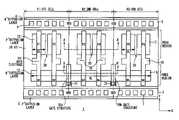
- FIG. 3is a plan view showing a pattern structure of a semiconductor device 1 according to the first embodiment of the present invention.
- a power supply line 2 for supplying a power supply voltage VDD and a ground line 3 for supplying a ground voltage GNDare arranged to extend in an X-direction.
- the power supply line 2is connected to an N-type diffusion layer 4 via contacts 6 to apply a power supply voltage as a substrate voltage.
- the ground line 3is connected to a P-type diffusion layer 5 via contacts 7 to apply a ground voltage as the substrate voltage.
- a plurality of PMOS transistors P 1 to P 6 and a plurality of NMOS transistors N 1 to N 6are formed in a region put between the power supply line 2 and the ground line 3 .
- the plurality of PMOS transistors P 1 to P 6are formed in a PMOS region to be aligned with each other along an X-direction.
- the plurality of NMOS transistors N 1 to N 6are formed in a NMOS region to be aligned with each other along the X-direction.
- a plurality of gate electrodes 10are formed for the plurality of PMOS transistors P 1 to P 6 and the plurality of NMOS transistors N 1 to N 6 . These gate electrodes 10 are formed to extend in a Y-direction orthogonal to the X-direction. Also, each of the gate electrodes 10 is shared by one PMOS transistor and one NMOS transistor. In the PMOS region, P-type diffusion layers 12 are formed to put the gate electrode 10 therebetween. Also, in the NMOS region, N-type diffusion layers 13 are formed to put the gate electrode 10 therebetween. Further, a STI structure 20 is formed as an element separation structure.
- each of the plurality of PMOS transistors P 1 to P 6is surrounded by the STI structure 20 .
- the STI structure 20is formed between the PMOS transistors P 1 and P 2 .
- the plurality of NMOS transistors N 1 to N 6are surrounded as a whole by the STI structure 20 .
- the STI structure 20is not formed between the NMOS transistors N 2 and N 3 . That is, the plurality of NMOS transistors N 1 to N 6 are continuously formed to be adjacent to each other and constitute a “NMOS transistor group”. In other words, one NMOS transistor group includes a large number of NMOS transistors.
- one PMOS transistor groupincludes only one PMOS transistor.
- the length of one transistor group in the X-directionis defined to be “diffusion layer length DL”.
- the diffusion layer length DLcan be defined to be a distance between the STI structures 20 in the X-direction.
- the diffusion layer length DL in the NMOS transistor groupis longer than the diffusion layer length DL in the PMOS transistor group.
- each of the PMOS transistorsis separated by using the STI structure 20 .
- Each of the plurality of NMOS transistors of the NMOS transistor groupshould be separated.
- a separation structure other than the STI structure 20should be employed.
- a gate structure 30is formed at a predetermined position in the NMOS region.
- the gate structure 30is located in a region between adjacent NMOS transistors.
- the gate structure 30is formed on the N-type diffusion layer 13 to extend in the Y-direction, like the gate electrode 10 .
- the gate structure 30is connected to the ground line 3 or the P-type diffusion layer 5 that is connected to the ground line 3 via a contact 31 . That is, the gate structure 30 is grounded and the voltage thereof is fixed to the ground voltage GND. Since the voltage of the gate structure 30 is the ground voltage, its gate structure 30 is equivalent to a transistor in OFF state. Therefore, it is possible to isolate the NMOS transistors themselves at a predetermined position in the NMOS region without using the STI structure 20 . For example, a gate structure 30 a isolates a set of the NMOS transistors N 1 and N 2 from a set of the NMOS transistors N 3 and N 4 .
- a gate structure 30 bisolates a set of the NMOS transistors N 3 and N 4 from a set of the NMOS transistors N 5 and N 6 .
- element isolation for NMOS transistorscan be realized using the gate structure 30 in place of the STI structure 20 .
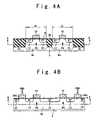
- FIG. 4Ais a cross sectional view of the semiconductor device along the line A-A′ in FIG. 3 .
- the PMOS transistors P 3 and P 4are formed on N-type regions 8 n of a substrate 8 adjacently to each other.
- the gate electrode 10is formed on the substrate 8 via a gate insulating film 9 .
- the P-type diffusion layers 12are formed in the N-type regions 8 n of the substrate 8 under the gate electrode 10 .
- Each of PMOS transistorsis surrounded by the STI structure 20 , and the STI structure 20 is formed in the substrate 8 between the PMOS transistors P 3 and P 4 .
- the length of a region surrounded by the STI structure 20is a diffusion layer length DL.
- FIG. 4Bis a sectional view of the semiconductor device along the line B-B′ in FIG. 3 .
- the NMOS transistors N 3 and N 4are formed on a P-type region 8 p of the substrate 8 adjacently to each other.
- the gate electrode 10is formed on the substrate 8 via the gate insulating film 9 .
- the N-type diffusion layers 13are formed in the P-type region 8 p of the substrate 8 in a region under the gate electrode 10 .
- the gate structures 30 a and 30 bare formed on the substrate 8 via the gate insulating film 9 .
- the N-type diffusion layers 13are formed in the substrate 8 in region below the gate structure 30 .
- the ground voltage GNDis applied to the gate structures 30 a and 30 b.
- the semiconductor device 1 shown in FIG. 3may be used in a gate array fashion.
- the semiconductor device 1 shown in FIG. 3may be provided as a foundation layer of ASIC (Application Specific Integrated Circuit).
- ASICApplication Specific Integrated Circuit
- its foundation layeris used in common to many purposes and wirings meeting user requirements are formed in a customized layer as an upper layer of the foundation layer. With this configuration, a desired LSI is obtained in a short time.
- the PMOS transistorsare formed one by one to be surrounded by an element separation STI structure 20 .
- the diffusion layer length DLbecomes minimum and characteristics of ON current can be improved as shown in FIG. 2 .
- the NMOS transistorsare arranged continuously to constitute the NMOS transistor group. In the NMOS transistor group, each of the NMOS transistors is not isolated by the STI structure 20 . Therefore, the diffusion layer length DL becomes longer and characteristics of ON current can be improved as shown in FIG. 2 . In this way, characteristics of ON current can be improved in both the PMOS transistors and the NMOS transistors. Since driving capabilities of both the PMOS transistors and the NMOS transistors are improved, the delay time is reduced.
- a voltage of the gate structure 30 formed in the NMOS regionis fixed to the ground voltage GND.
- the element separation or isolationcan be carried out by using the gate structure 30 without using the STI structure 20 that is related to deterioration of characteristics of ON current.
- elongation of the diffusion layer length DL in the NMOS region and the element isolation in the NMOS regionare both accomplished by the gate structure 30 according to the first embodiment.
- the element separation or isolationis realized in the NMOS region, it is possible to handle the desired number of NMOS transistors in the NMOS transistor group.
- the designingcan be carried out freely.
- the gate structures 30 a and 30 bmay simply be formed at the positions shown in FIG. 3 .
- the first embodimentit is possible to carry out element separation without consideration of effects by the diffusion layer length DL. Therefore, characteristic of ON current is improved and at the same time, the degree of freedom in designing is improved.
- the diffusion layer length DL in the PMOS transistoris shortened and the diffusion layer length DL in the NMOS transistors is lengthened. Therefore, the diffusion layer lengths DL between the PMOS region and the NMOS region are different. If the element isolation is not made for the NMOS transistors, a dimension of one PROS transistor and a dimension of one NMOS transistor are different. As a result, when one NMOS transistor is allocated to one PMOS transistor, a useless region will be generated due to their dimension difference.
- the element isolationis realized by the gate structure 30 , it is possible to make the dimension of one PMOS transistor coincident with that of one NMOS transistor. Thus, since no useless region is generated, the reduction in chip area usage efficiency is prevented.
- the semiconductor device 1can be designed by cell-base technique and manufactured.
- the structure shown in FIG. 3can be realized by a combination of a first cell 41 , a second cell 42 and a third cell 43 .
- the first cell 41includes PMOS transistors P 1 and P 2 , NMOS transistors N 1 and N 2 and half of the gate structure 30 a .
- the second cell 42includes PMOS transistors P 3 and P 4 , NMOS transistors N 3 and N 4 , half of the gate structure 30 a and half of the gate structure 30 b .
- the third cell 43includes PMOS transistors P 5 and P 6 , NMOS transistors N 5 and N 6 and half of the gate structure 30 b .
- the first cell 41 and the second cell 42are arranged so that the gate structure 30 a is formed when they are adjacent to each other.
- the second cell 42 and the third cell 43are arranged so that the gate structure 30 b is formed when they are adjacent to each other.
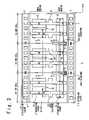
- FIG. 5is a plan view showing arrangement of cells in the semiconductor device according to the second embodiment of the present invention. As shown in FIG. 5 , a plurality of fourth cells 44 and a plurality of fifth cells 45 are arranged in the X-direction.
- the fourth cell 44is a basic cell.
- the fifth cell 45is an element isolation cell to be used for the element isolation.
- the element isolation cell 45is arranged adjacent to the plurality of basic cells 44 .
- the PMOS transistors and the NMOS transistors shown in FIG. 5are formed in the basic cell (fourth cell). Specifically, the gate electrode 10 is formed to extend in the Y-direction orthogonal to the X-direction. One gate electrode 10 is shared by one PMOS transistor and one NMOS transistor. Further, the P-type diffusion layers 12 are formed in the PMOS region to put the gate electrode 10 therebetween, and the N-type diffusion layers 13 are formed in the NMOS region to put the gate electrode 10 therebetween.
- the N-type diffusion layer (group) 13is formed to extend to an end portion of the basic cell 44 in the X-direction. That is, the N-type diffusion layer 13 is in contact with at least one of two opposing sides of the basic cell 44 . Meanwhile, the PMOS transistor is surrounded by the STI structure 20 .
- the gate structure 30 shown in FIG. 5is formed in the element isolation cell (fifth cell) 45 . Specifically, the gate structure 30 is located in a region put between two N-type diffusion layers 13 (N-type diffusion layer group). The two N-type diffusion layers 13 extend to the ends of the element isolation cell 45 in the X-direction and an opposing direction. That is, each of two N-type diffusion layers 13 is contact with one of two opposing sides of the element isolation cell 45 .
- the gate structure 30is connected to the ground line 3 and voltage thereof is fixed to the ground voltage GND.
- the N-type diffusion layers 13 of a certain basic cell 44are lined up with the N-type diffusion layers 13 of other basic cell 44 along the X-direction.
- the N-type diffusion layers 13 of the basic cell 44are lined up with the N-type diffusion layers 13 of the element isolation cell 45 in the X-direction.
- the basic cells 44 and the element isolation cells 45are arranged continuously along the X-direction, the N-type diffusion layers 13 are lined up. Therefore, it is possible to elongate the diffusion layer length DL to a desired length in the NMOS region by repeatedly providing the basic cells 44 and the element isolation cells 45 .
- the element isolation cell 45may simply be inserted appropriately at a position where electrical isolation is necessary.
- FIG. 6is a sectional view of the semiconductor device along the line A-A′ and the line B-B′ in FIG. 5 .
- the PMOS transistors and the NMOS transistorsare formed on the substrate 8 .
- the gate electrode 10is formed on the substrate 8 via the gate insulating film 9 .
- the P-type diffusion layers 12 and the N-type diffusion layers 13are formed in the substrate 8 to be adjacent to a region under the gate electrode 10 .
- the PMOS transistorsare surrounded by the STI structure 20 and the STI structure 20 is formed in the substrate 8 between adjacent PMOS transistors. It is supposed that the length of the basic cell 4 in the X-direction is Wa.
- one basic cell 44includes two PMOS transistors and two NMOS transistors.
- the number of transistorsis not necessarily limited to two.
- one basic cell 44may include one PMOS transistor and one NMOS transistor.
- one basic cell 44may include four PMOS transistors and four NMOS transistors. Designing of the semiconductor device 1 is carried out by arranging the basic cells 44 and the element isolation cells 45 appropriately.
- FIG. 7is a block diagram showing a system (CAD) for supporting design of the semiconductor device 1 .
- This semiconductor device design supporting system 50includes a cell library 40 , a processing unit 51 , a memory 52 , a design program 53 , an input unit 54 and a display unit 55 .
- Data showing a plurality of cellsare stored as a library in the cell library 40 .
- the fourth cell 44 and the fifth cell 45 for the element isolationare included in the plurality of cells. Further, as the plurality of cells, the first cell 41 to the third cell 43 may be used.
- the cell library 40is realized by, for example, a hard disc unit.
- the memory 52is used as a working area in which a layout is formed and a layout space is constructed therein.
- the processing unit 51can access the cell library 40 and the memory 52 .
- the design program (automatic layout tool) 53is a computer program (software product) executed by the processing unit 51 .
- As the input unit 54a keyboard or a mouse is exemplified.
- a usercan enter various commands using the input unit 54 while referring to information displayed on the display unit 55 .
- the usercan produce a layout data showing the layout of the semiconductor device 1 by use of semiconductor device designing system 50 .
- the processing unit 51executes the following operation according to commands given from the design program 53 .
- the processing unit 51builds up a layout space on the memory 52 .
- the processing unit 51reads out a data showing a cell to be used from the cell library 40 .
- the cellis then arranged at a predetermined position on the layout space.
- the basic cell 44is arranged repeatedly in the X-direction.
- the element isolation cell 45is arranged to be adjacent to the basic cells 44 arranged as mentioned.
- the element isolation cell 45may be inserted appropriately in the position that needs electrical isolation. Following this, wirings for connecting transistors are provided according to a logic circuit to be designed and manufactured.
- FIG. 8Ashows an example of wirings to be used for the structure of inverters as the semiconductor device according to the third embodiment of the present invention.
- a source of the PMOS transistor P 1is connected to a power supply line by a wiring 61 .
- a source of the PMOS transistor P 2is connected to the power supply line by a wiring 62 .
- a source of the NMOS transistor N 1is connected to a ground line by a wiring 63 .
- a source of the NMOS transistor N 2is connected to the ground line by a wiring 64 .
- a drain of the PMOS transistor P 1is connected to a drain of the NMOS transistor N 1 by a wiring 65 .
- a drain of the PMOS transistor P 2is connected to a drain of the NMOS transistor N 2 by a wiring 66 .
- the wiring 65 and the wiring 66are connected to each other. Further, a gate electrode 10 - 1 of the PMOS transistor P 1 and the NMOS transistor N 1 , and a gate electrode 10 - 2 of the PMOS transistor P 2 and the NMOS transistor N 2 are connected via a wiring 67 . With this configuration, a so-called “ ⁇ 2 inverter” is constituted.
- a source of the PMOS transistor P 3is connected to the power supply line by a wiring 71 .
- a source of the PMOS transistor P 4is connected to the power supply line by a wiring 72 .
- a source of the NMOS transistor N 3is connected to the ground line by a wiring 73 .
- a source of the NMOS transistor N 4is connected to the ground line by a wiring 74 .
- a drain of the PMOS transistor P 3is connected to a drain of the NMOS transistor N 3 by a wiring 75 .
- a drain of the PMOS transistor P 4is connected to a drain of the NMOS transistor N 4 by a wiring 76 .
- the wiring 75 and the wiring 76are connected to each other.
- a gate electrode 10 - 3 of the PMOS transistor P 3 and the NMOS transistor N 3 , and a gate electrode 10 - 4 of the PMOS transistor P 4 and the NMOS transistor N 4are connected via a wiring 77 .
- a so-called “ ⁇ 2 inverter”is constituted.
- FIG. 8Bis a top plan view showing another structure of inverters as the semiconductor device according to the fourth embodiment of the present invention.
- identical reference numerals or symbolsare used for the same components as those shown in FIG. 8A and description thereof is omitted.
- gate electrodes 10 - 1 to 10 - 4are connected to each other via a wiring 80 . With this configuration, a so-called “ ⁇ 4 inverter” is constituted. An inverter having greater driving capability than the inverter shown in FIG. 8A is thus realized.
- invertersIn the LSI, various driving capabilities are required for inverters. According to the present embodiments, it is possible to realize inverters with various driving capabilities by changing wirings between transistors. Further, when a so-called “ ⁇ 8 inverter” is required, the number of repetitions of the basic cell 44 should be altered. Not limited to inverters, it is possible to design and manufacture various logic circuits by altering the number of times of repetition of the basic cell 44 and position of the element isolation cell 45 . Further, it is possible to carry out the element isolation by inserting the element isolation cell 45 having the gate structure 30 in the desired position without effects by the diffusion layer length DL. According to the present invention, the degree of freedom in designing is improved. Therefore, it is possible to cope minutely with user's needs.
- the gate electrode 10is preferably formed to extend along the Y-direction.
- DFMDesign for Manufacturing
- a design ruleis prepared considering a manufacturing process. For example, in order to reduce a circuit region, when a gate electrode is designed to pass through a complicated route, there is a possibility of generation of deviation in the width of gate polysilicon in actual manufacturing stage. That is, a gate electrode with a complicated configuration may result in deviation in the gate length L of transistors at manufacturing.
- the deviation in the gate length Lis one of factors of deviation in characteristics of transistors.
- the gate electrode 10be designed to be a linear straight line at designing stage. With this consideration, the deviation in the gate length L is suppressed at actual designing stage. Therefore, performances of transistors are improved.
- time and effort for considering effects of the diffusion layer length DL (STI structure stress) and deviation in the gate length Lare eliminated.
- FIG. 9is a top plan view of the semiconductor device according to the fifth embodiment of the present invention.
- a gate structure 90is used instead of the gate structure 30 connected to the ground line 3 .
- a gate structure 90 ais arranged between NMOS transistors N 2 and N 3 .
- a gate structure 90 bis arranged between NMOS transistors N 3 and N 4 .
- FIG. 10Ais a sectional view of the semiconductor device according to the fifth embodiment along the line A-A′ in FIG. 9 .
- the PMOS transistors P 3 and P 4are formed on the N-type regions 8 n of the substrate 8 adjacently to each other.
- the gate electrode 10is formed on the substrate 8 via the gate insulating film 9 .
- the P-type diffusion layers 12are formed in the N-type regions 8 n of the substrate 8 to be adjacent to a region under the gate electrode 10 .
- Each of the PMOS transistorsis surrounded by the STI structure 20 and the STI structure 20 is formed in the substrate 8 between the PMOS transistors P 3 and P 4 .
- FIG. 10Bis a sectional view of the semiconductor device according to the fifth embodiment along the line B-B′ in FIG. 9 .
- the gate electrode 10is formed on the substrate 8 via the gate insulating film 9 .
- the N-type diffusion layers 13are formed in the substrate 8 to be adjacent to a region under the gate electrode 10 .
- the gate structures 90 a and 90 bare formed on the substrate 8 via the gate insulating film 9 .
- the N-type diffusion layers 13are formed in the substrate 8 to be adjacent to a region under the gate structure 90 .
- power supply voltage VDDis applied to the gate structures 90 a and 90 b.
- the gate structure 90By using the gate structure 90 as mentioned above, it is possible to realize a circuit in which the number of PMOS transistors and the number of NMOS transistors are asymmetrical. For example, it is possible to realize a circuit of two PMOS transistors and four NMOS transistors.
- the grounded gate structure 30may simply be formed in the position in which electrical isolation is needed, with a similar manner as the first embodiment. With this configuration, the element isolation is also realized.
- Such a structureis possible simply because no STI structure 20 is formed in the NMOS region.
- the gate structureis formed between adjacent NMOS transistors instead of the STI structure 20 , and a voltage to be applied to the gate structure may be determined depending on the desired circuit.
- the characteristic of ON currentcan be improved for both the PMOS transistors and the NMOS transistors. Since driving capabilities of both PMOS transistors and the NMOS transistors can be improved, a delay time is reduced.
- the semiconductor device 1 ′may be designed and manufactured based on the cell-base technique in a similar manner as the second embodiment. In such a case, in addition to the fourth cell (basic cell) 44 and the fifth cell (element isolation cell) 45 , a sixth cell 46 shown in FIG. 9 may be used. It becomes possible to realize various logic circuits by disposing the fourth cell 44 repeatedly and by inserting the fifth cell 45 or the sixth cell 46 at the desired position.
Landscapes
- Metal-Oxide And Bipolar Metal-Oxide Semiconductor Integrated Circuits (AREA)
- Design And Manufacture Of Integrated Circuits (AREA)
- Element Separation (AREA)
Abstract
Description
1. Field of the Invention
The present invention relates to a semiconductor device. More particularly, the present invention relates to a semiconductor device including PMOS transistors and NMOS transistors, and a manufacturing method of the same.
2. Description of the Related Art
It is indispensable in designing an LSI (Large-Scaled Integrated Semiconductor Device) to use a computer for the sake of reduction in time for designing and confirmation and to eliminate man-caused mistakes. A semiconductor device design supporting system using the computer in this manner is referred to as a CAD (Computer Aided Design) system. According to a LSI designing method of cell base, cells of a plurality of types are configured as a library. A designer executes designing of LSI by utilizing CAD and allocating a desired cell in a layout space defined on the computer.
In a semiconductor device field, in many cases, a plurality of transistors are used collectively. For this reason, each of the basic cells is formed in such a manner that a “transistor group” composed of a plurality of transistors is surrounded by aSTI structure 120. For example, inFIG. 1 , the PMOS transistor group P1 and P2 is surrounded by theSTI structure 120, and the PMOS transistor group P3 and P4 is surrounded by theSTI structure 120. That is, the PMOS transistor group P1 and P2 and the PMOS transistor group P3 and P4 are isolated or separated by theSTI structures 120. Further, an NMOS transistor group N1 and N2 is surrounded by theSTI structure 120 and an NMOS transistor group N3 and N4 is surrounded by theSTI structure 120. That is, the NMOS transistor group N1 and N2 and the NMOS transistor group N3 and N4 are isolated by theSTI structures 120. Meanwhile, the length of one transistor group in the X-direction is referred to as a “diffusion layer length DL”. In other words, the diffusion layer length DL can be defined as the length betweenSTI structures 120 in the X-direction.
In conjunction with the above description, a semiconductor device is disclosed in Japanese Laid open Patent Publication (JP-P2003-203989A). In this conventional example, the semiconductor device includes P-channel field effect transistors connected in a lattice form. In the semiconductor device of this type, a long active region extending over a plurality of transistors is divided for every gate electrode such that a compression stress is applied to a channel portion of the P-channel field effect transistor. A sufficiently thin STI structure is arranged between the gate electrodes.
Also, a semiconductor integrated circuit device is disclosed in Japanese Laid Open Patent Publication (JP-P2001-345430A), in which element structure MISFET and element isolation MISFET are formed on a main surface of a semiconductor substrate. The element structure MISFET and the element isolation MISFET of include a source and a drain which are formed in a semiconductor substrate, a gate insulating film formed between the source and the drain on the semiconductor substrate, and a doped gate electrode formed on the gate insulating film. Besides, a difference in work function between the gate electrode of the element isolation MISFET and the main surface of the semiconductor substrate is greater than a difference in work function between the gate electrode of the element constitution MISFET and the main surface of the semiconductor substrate.
A stress generated due to isolation of elements by the STI structure (hereinafter, to be also referred to as a STI structure stress) changes the crystal structure. The change in the crystal structure has an influence upon characteristics of transistors, for example, driving capability of a transistor. In recent years, miniaturization of the element has made remarkable progress, and the STI structure stress has become a significant problem. Namely, as the element is miniaturized, the STI structure stress that influences the driving capability of the transistor has become one of factors which cannot be ignored. For example, it is known that magnitude of ON current Ion of the transistor (drain current) fluctuates depending on change in the STI structure stress. Since the STI structure stress depends upon the above diffusion layer length DL as a distance between STI structures, the diffusion layer length DL has an effect upon magnitude of ON current Ion.
In consideration of miniaturization of the elements, it is desired to provide a technique that can improve the characteristics of ON current (drain current) as much as possible for both the PMOS transistors and the NMOS transistors. When the diffusion layer length DL is simply elongated in the NMOS transistor, many NMOS transistors are arranged in a region between the STI structures. In this case, it is not possible to use a desired number of NMOS transistors among many NMOS transistors. In other words, if the diffusion layer length DL is simply elongated, isolation of a desired number of elements is not possible and handling of a desired number of elements is not possible accordingly.
In an aspect of the present invention, a semiconductor device includes a plurality of PMOS transistors formed on a semiconductor substrate; and a plurality of NMOS transistors formed on the semiconductor substrate. The plurality of PMOS transistors are electrically isolated from each other by a device isolation structure formed in the semiconductor substrate. The plurality of NMOS transistors are continuously formed in a first direction such that a sequence of N-type diffusion layers of the plurality of NMOS transistors extends in the first direction. One of the plurality of PMOS transistors and one of the plurality of NMOS transistors share a gate electrode.
Here, the semiconductor device may further include gate structures formed on the semiconductor substrate to extend in a second direction orthogonal to the first direction over the sequence of the N-type diffusion layers.
In this case, a voltage of the gate structures may be fixed to a ground voltage. Instead, the voltage of the gate structures may be fixed to a power supply voltage.
The gate structures may isolate the plurality of NMOS transistors in units of a predetermined number of NMOS transistors. In this case, the predetermined number may be one of two, four and six.
Also, two of the gate electrodes of the two NMOS transistors may be connected to each other. Also, four of the gate electrodes of the four NMOS transistors may be connected to each other.
Also, in another aspect of the present invention, a semiconductor device includes a plurality of transistor cells arranged in a first direction. Each of the plurality of transistor cells includes a first PMOS transistor formed on a semiconductor substrate; a second PMOS transistor formed on the semiconductor substrate adjacently to the first PMOS transistor; a device isolation structure configured to isolate the first and second PMOS transistors from each other; a first NMOS transistor formed on the semiconductor substrate; and a second NMOS transistor formed on the semiconductor substrate adjacently to the first NMOS transistor. N-type diffusion layers of the first and second NMOS transistors are arranged in the first direction.
Here, the N-type diffusion layers may reach at least one of two opposing sides of the cell orthogonal to the first direction. Especially, the N-type diffusion layers may reach the two opposing sides of the cell orthogonal to the first direction.
In this case, the cell may further include a half of a gate structure provided on the semiconductor substrate to extend over the N-type diffusion layers in a second direction orthogonal to the first direction. A remaining half of the gate structure is provided in one cell adjacent to the cell.
Also, the semiconductor device may further include a device isolation cell provided for every predetermined number of the plurality of transistor cells. The device isolation cell includes a gate structure provided on the semiconductor substrate to extend in a second direction orthogonal to the first direction; and N-type diffusion layers formed in the semiconductor substrate to be adjacent to the gate structure. The N-type diffusion layers of the device isolation cell reach two opposing sides of the device isolation cell orthogonal to the first direction.
Here, the predetermined number may be one of two, four and six.
Also, two of the gate electrodes of the two NMOS transistors may be connected to each other, and four of the gate electrodes of the fourth NMOS transistors may be connected to each other.
In another aspect of the present invention, a method of manufacturing a semiconductor device, is achieved by (A) providing a basic cell and a device isolation cell; wherein the basic cell includes: a PMOS transistor surrounded by the device isolation structure; and a first N-type diffusion layer of an NMOS transistor configured to contacting one of two opposing sides of the basic cell, and the device isolation cell includes: a second group of N-type diffusion layers configured to contact two opposing sides of the device isolation cells; and a gate structure provided on a semiconductor substrate in a region put in the second group of N-type diffusion layers, and the first N-type diffusion layer of the basic cell is formed to be aligned with the first N-type diffusion layer of another basic cell, and the second group of N-type diffusion layers the device isolation cell in a first direction, by (B) arranging the basic cell repeatedly in the first direction; and by (C) arranges the device isolation cell to be adjacent to the arranged basic cell in the first direction.
Here, the gate structure of the device isolation cell may be grounded.
Also, the basic cell may have a gate electrode of the PMOS transistor and the NMOS transistor, and the gate electrode may be formed to extend in a second direction orthogonal to the first direction.
Hereinafter, a semiconductor device and a method of manufacturing the same according to the present invention will be described in detail with reference to the attached drawings. The semiconductor device according to the present invention includes PMOS transistors and NMOS transistors.
A plurality ofgate electrodes 10 are formed for the plurality of PMOS transistors P1 to P6 and the plurality of NMOS transistors N1 to N6. Thesegate electrodes 10 are formed to extend in a Y-direction orthogonal to the X-direction. Also, each of thegate electrodes 10 is shared by one PMOS transistor and one NMOS transistor. In the PMOS region, P-type diffusion layers12 are formed to put thegate electrode 10 therebetween. Also, in the NMOS region, N-type diffusion layers13 are formed to put thegate electrode 10 therebetween. Further, aSTI structure 20 is formed as an element separation structure. According to the present invention, in the PMOS region, each of the plurality of PMOS transistors P1 to P6 is surrounded by theSTI structure 20. For example, theSTI structure 20 is formed between the PMOS transistors P1 and P2. On the other hand, in the NMOS region, the plurality of NMOS transistors N1 to N6 are surrounded as a whole by theSTI structure 20. For example, theSTI structure 20 is not formed between the NMOS transistors N2 and N3. That is, the plurality of NMOS transistors N1 to N6 are continuously formed to be adjacent to each other and constitute a “NMOS transistor group”. In other words, one NMOS transistor group includes a large number of NMOS transistors. Meanwhile, one PMOS transistor group includes only one PMOS transistor. The length of one transistor group in the X-direction is defined to be “diffusion layer length DL”. Further, the diffusion layer length DL can be defined to be a distance between theSTI structures 20 in the X-direction. According to the present invention, the diffusion layer length DL in the NMOS transistor group is longer than the diffusion layer length DL in the PMOS transistor group.
As shown above, each of the PMOS transistors is separated by using theSTI structure 20. Each of the plurality of NMOS transistors of the NMOS transistor group should be separated. Here, in order to keep the diffusion layer length DL long to a maximum extent, a separation structure other than theSTI structure 20 should be employed. To attain this, according to the present invention, as shown inFIG. 3 , agate structure 30 is formed at a predetermined position in the NMOS region. Thegate structure 30 is located in a region between adjacent NMOS transistors. Also, thegate structure 30 is formed on the N-type diffusion layer 13 to extend in the Y-direction, like thegate electrode 10. Thegate structure 30 is connected to theground line 3 or the P-type diffusion layer 5 that is connected to theground line 3 via acontact 31. That is, thegate structure 30 is grounded and the voltage thereof is fixed to the ground voltage GND. Since the voltage of thegate structure 30 is the ground voltage, itsgate structure 30 is equivalent to a transistor in OFF state. Therefore, it is possible to isolate the NMOS transistors themselves at a predetermined position in the NMOS region without using theSTI structure 20. For example, agate structure 30aisolates a set of the NMOS transistors N1 and N2 from a set of the NMOS transistors N3 and N4. Further, agate structure 30bisolates a set of the NMOS transistors N3 and N4 from a set of the NMOS transistors N5 and N6. In this way, according to the present invention, element isolation for NMOS transistors can be realized using thegate structure 30 in place of theSTI structure 20.
Also,FIG. 4B is a sectional view of the semiconductor device along the line B-B′ inFIG. 3 . As shown inFIG. 4B , the NMOS transistors N3 and N4 are formed on a P-type region 8pof thesubstrate 8 adjacently to each other. In each of the NMOS transistors, thegate electrode 10 is formed on thesubstrate 8 via thegate insulating film 9. The N-type diffusion layers13 are formed in the P-type region 8pof thesubstrate 8 in a region under thegate electrode 10. Further, thegate structures substrate 8 via thegate insulating film 9. The N-type diffusion layers13 are formed in thesubstrate 8 in region below thegate structure 30. Further, the ground voltage GND is applied to thegate structures
By using thesemiconductor device 1 as shown above, and connecting appropriately the PMOS transistors and the NMOS transistors, various logic circuits are realized. Thesemiconductor device 1 shown inFIG. 3 may be used in a gate array fashion. Thesemiconductor device 1 shown inFIG. 3 may be provided as a foundation layer of ASIC (Application Specific Integrated Circuit). In case of ASIC, its foundation layer is used in common to many purposes and wirings meeting user requirements are formed in a customized layer as an upper layer of the foundation layer. With this configuration, a desired LSI is obtained in a short time.
As described above, according to thesemiconductor device 1 according to the first embodiment of the present invention, the PMOS transistors are formed one by one to be surrounded by an elementseparation STI structure 20. For this reason, the diffusion layer length DL becomes minimum and characteristics of ON current can be improved as shown inFIG. 2 . On the other hand, the NMOS transistors are arranged continuously to constitute the NMOS transistor group. In the NMOS transistor group, each of the NMOS transistors is not isolated by theSTI structure 20. Therefore, the diffusion layer length DL becomes longer and characteristics of ON current can be improved as shown inFIG. 2 . In this way, characteristics of ON current can be improved in both the PMOS transistors and the NMOS transistors. Since driving capabilities of both the PMOS transistors and the NMOS transistors are improved, the delay time is reduced.
Also, according to the first embodiment, a voltage of thegate structure 30 formed in the NMOS region is fixed to the ground voltage GND. Thus, it is possible to electrically isolate adjacent NMOS transistors from each other at the position of thegate structure 30. That is, the element separation or isolation can be carried out by using thegate structure 30 without using theSTI structure 20 that is related to deterioration of characteristics of ON current. Thus, elongation of the diffusion layer length DL in the NMOS region and the element isolation in the NMOS region are both accomplished by thegate structure 30 according to the first embodiment. Further, since the element separation or isolation is realized in the NMOS region, it is possible to handle the desired number of NMOS transistors in the NMOS transistor group. Thus, the designing can be carried out freely. For example, when transistors are to be used in units of two, thegate structures FIG. 3 . According to the first embodiment, it is possible to carry out element separation without consideration of effects by the diffusion layer length DL. Therefore, characteristic of ON current is improved and at the same time, the degree of freedom in designing is improved.
Further, according to the first embodiment, reduction of chip area usage efficiency in layout can be prevented. The diffusion layer length DL in the PMOS transistor is shortened and the diffusion layer length DL in the NMOS transistors is lengthened. Therefore, the diffusion layer lengths DL between the PMOS region and the NMOS region are different. If the element isolation is not made for the NMOS transistors, a dimension of one PROS transistor and a dimension of one NMOS transistor are different. As a result, when one NMOS transistor is allocated to one PMOS transistor, a useless region will be generated due to their dimension difference. However, according to the first embodiment, since the element isolation is realized by thegate structure 30, it is possible to make the dimension of one PMOS transistor coincident with that of one NMOS transistor. Thus, since no useless region is generated, the reduction in chip area usage efficiency is prevented.
Thesemiconductor device 1 according to the present invention can be designed by cell-base technique and manufactured. For example, the structure shown inFIG. 3 can be realized by a combination of afirst cell 41, asecond cell 42 and athird cell 43. Thefirst cell 41 includes PMOS transistors P1 and P2, NMOS transistors N1 and N2 and half of thegate structure 30a. Thesecond cell 42 includes PMOS transistors P3 and P4, NMOS transistors N3 and N4, half of thegate structure 30aand half of thegate structure 30b. Thethird cell 43 includes PMOS transistors P5 and P6, NMOS transistors N5 and N6 and half of thegate structure 30b. Thefirst cell 41 and thesecond cell 42 are arranged so that thegate structure 30ais formed when they are adjacent to each other. Further, thesecond cell 42 and thethird cell 43 are arranged so that thegate structure 30bis formed when they are adjacent to each other.
Further, thesemiconductor device 1 according to the present invention can be also realized by a combination of cell groups of different types.FIG. 5 is a plan view showing arrangement of cells in the semiconductor device according to the second embodiment of the present invention. As shown inFIG. 5 , a plurality offourth cells 44 and a plurality offifth cells 45 are arranged in the X-direction. Thefourth cell 44 is a basic cell. On the other hand, thefifth cell 45 is an element isolation cell to be used for the element isolation. Theelement isolation cell 45 is arranged adjacent to the plurality ofbasic cells 44.
The PMOS transistors and the NMOS transistors shown inFIG. 5 are formed in the basic cell (fourth cell). Specifically, thegate electrode 10 is formed to extend in the Y-direction orthogonal to the X-direction. Onegate electrode 10 is shared by one PMOS transistor and one NMOS transistor. Further, the P-type diffusion layers12 are formed in the PMOS region to put thegate electrode 10 therebetween, and the N-type diffusion layers13 are formed in the NMOS region to put thegate electrode 10 therebetween. The N-type diffusion layer (group)13 is formed to extend to an end portion of thebasic cell 44 in the X-direction. That is, the N-type diffusion layer 13 is in contact with at least one of two opposing sides of thebasic cell 44. Meanwhile, the PMOS transistor is surrounded by theSTI structure 20.
Thegate structure 30 shown inFIG. 5 is formed in the element isolation cell (fifth cell)45. Specifically, thegate structure 30 is located in a region put between two N-type diffusion layers13 (N-type diffusion layer group). The two N-type diffusion layers13 extend to the ends of theelement isolation cell 45 in the X-direction and an opposing direction. That is, each of two N-type diffusion layers13 is contact with one of two opposing sides of theelement isolation cell 45. Thegate structure 30 is connected to theground line 3 and voltage thereof is fixed to the ground voltage GND.
As shown inFIG. 5 , the N-type diffusion layers13 of a certainbasic cell 44 are lined up with the N-type diffusion layers13 of otherbasic cell 44 along the X-direction. Also, the N-type diffusion layers13 of thebasic cell 44 are lined up with the N-type diffusion layers13 of theelement isolation cell 45 in the X-direction. Conversely, it is designed that when thebasic cells 44 and theelement isolation cells 45 are arranged continuously along the X-direction, the N-type diffusion layers13 are lined up. Therefore, it is possible to elongate the diffusion layer length DL to a desired length in the NMOS region by repeatedly providing thebasic cells 44 and theelement isolation cells 45. Theelement isolation cell 45 may simply be inserted appropriately at a position where electrical isolation is necessary.
Thememory 52 is used as a working area in which a layout is formed and a layout space is constructed therein. Theprocessing unit 51 can access thecell library 40 and thememory 52. The design program (automatic layout tool)53 is a computer program (software product) executed by theprocessing unit 51. As theinput unit 54, a keyboard or a mouse is exemplified. A user (design person) can enter various commands using theinput unit 54 while referring to information displayed on thedisplay unit 55. The user can produce a layout data showing the layout of thesemiconductor device 1 by use of semiconductordevice designing system 50.
Theprocessing unit 51 executes the following operation according to commands given from thedesign program 53. First, theprocessing unit 51 builds up a layout space on thememory 52. Next, theprocessing unit 51 reads out a data showing a cell to be used from thecell library 40. The cell is then arranged at a predetermined position on the layout space. For example, as shown inFIG. 5 , thebasic cell 44 is arranged repeatedly in the X-direction. Then, at a predetermined position, theelement isolation cell 45 is arranged to be adjacent to thebasic cells 44 arranged as mentioned. Thus, it is possible to elongate the diffusion layer length DL to a desired length in the NMOS region by arranging thebasic cells 44 and theelement isolation cells 45 repeatedly. Theelement isolation cell 45 may be inserted appropriately in the position that needs electrical isolation. Following this, wirings for connecting transistors are provided according to a logic circuit to be designed and manufactured.
Further, a source of the PMOS transistor P3 is connected to the power supply line by awiring 71. A source of the PMOS transistor P4 is connected to the power supply line by awiring 72. A source of the NMOS transistor N3 is connected to the ground line by awiring 73. A source of the NMOS transistor N4 is connected to the ground line by awiring 74. A drain of the PMOS transistor P3 is connected to a drain of the NMOS transistor N3 by awiring 75. A drain of the PMOS transistor P4 is connected to a drain of the NMOS transistor N4 by awiring 76. Besides, thewiring 75 and thewiring 76 are connected to each other. Further, a gate electrode10-3 of the PMOS transistor P3 and the NMOS transistor N3, and a gate electrode10-4 of the PMOS transistor P4 and the NMOS transistor N4 are connected via a wiring77. With this configuration, a so-called “×2 inverter” is constituted.
In the LSI, various driving capabilities are required for inverters. According to the present embodiments, it is possible to realize inverters with various driving capabilities by changing wirings between transistors. Further, when a so-called “×8 inverter” is required, the number of repetitions of thebasic cell 44 should be altered. Not limited to inverters, it is possible to design and manufacture various logic circuits by altering the number of times of repetition of thebasic cell 44 and position of theelement isolation cell 45. Further, it is possible to carry out the element isolation by inserting theelement isolation cell 45 having thegate structure 30 in the desired position without effects by the diffusion layer length DL. According to the present invention, the degree of freedom in designing is improved. Therefore, it is possible to cope minutely with user's needs.
As shown inFIG. 5 , thegate electrode 10 is preferably formed to extend along the Y-direction. In recent years, concept of DFM (Design for Manufacturing) are attracting attentions. In the DFM, a design rule is prepared considering a manufacturing process. For example, in order to reduce a circuit region, when a gate electrode is designed to pass through a complicated route, there is a possibility of generation of deviation in the width of gate polysilicon in actual manufacturing stage. That is, a gate electrode with a complicated configuration may result in deviation in the gate length L of transistors at manufacturing. The deviation in the gate length L is one of factors of deviation in characteristics of transistors. For this reason, according to the concept of DFM, it is preferable that thegate electrode 10 be designed to be a linear straight line at designing stage. With this consideration, the deviation in the gate length L is suppressed at actual designing stage. Therefore, performances of transistors are improved. According to the present invention, time and effort for considering effects of the diffusion layer length DL (STI structure stress) and deviation in the gate length L are eliminated.
By using the gate structure90 as mentioned above, it is possible to realize a circuit in which the number of PMOS transistors and the number of NMOS transistors are asymmetrical. For example, it is possible to realize a circuit of two PMOS transistors and four NMOS transistors. As a matter of fact, the groundedgate structure 30 may simply be formed in the position in which electrical isolation is needed, with a similar manner as the first embodiment. With this configuration, the element isolation is also realized. Such a structure is possible simply because noSTI structure 20 is formed in the NMOS region. The gate structure is formed between adjacent NMOS transistors instead of theSTI structure 20, and a voltage to be applied to the gate structure may be determined depending on the desired circuit.
According to the fifth embodiment, in a similar manner to the first embodiment, the characteristic of ON current can be improved for both the PMOS transistors and the NMOS transistors. Since driving capabilities of both PMOS transistors and the NMOS transistors can be improved, a delay time is reduced. Further, thesemiconductor device 1′ may be designed and manufactured based on the cell-base technique in a similar manner as the second embodiment. In such a case, in addition to the fourth cell (basic cell)44 and the fifth cell (element isolation cell)45, asixth cell 46 shown inFIG. 9 may be used. It becomes possible to realize various logic circuits by disposing thefourth cell 44 repeatedly and by inserting thefifth cell 45 or thesixth cell 46 at the desired position.
Claims (14)
1. A semiconductor device comprising:
a plurality of PMOS transistors formed on a semiconductor substrate;
a plurality of NMOS transistors formed on said semiconductor substrate; and
a gate structure formed on said semiconductor substrate between an adjacent of said plurality of NMOS transistors to extend in a second direction perpendicular to a first direction over an N-type diffusion layer,
wherein said plurality of PMOS transistors are surrounded and electrically isolated from each other by a device isolation structure formed in said semiconductor substrate,
wherein said plurality of NMOS transistors are adjacent to each other and surrounded by said device isolation structure in said first direction such that said N-type diffusion layer of said plurality of NMOS transistors extends continuously with respect to said plurality of NMOS transistors in said first direction, and
wherein one of said plurality of PMOS transistors and one of said plurality of NMOS transistors share a gate electrode.
2. The semiconductor device according toclaim 1 , wherein a ground voltage is applied to said gate structure.
3. The semiconductor device according toclaim 1 , wherein a power supply voltage is applied to said gate structure.
4. The semiconductor device according toclaim 1 , wherein said gate structure isolates a predetermined number of said plurality of said NMOS transistors.
5. The semiconductor device according toclaim 4 , wherein the predetermined number is two.
6. The semiconductor device according toclaim 4 , wherein the predetermined number is four.
7. The semiconductor device according toclaim 4 , wherein the predetermined number is six.
8. The semiconductor device according toclaim 5 , wherein said gate electrode of said one of said plurality of NMOS transistors is connected to another gate electrode of another one of said plurality of NMOS transistors.
9. The semiconductor device according toclaim 6 , wherein four of said gate electrodes of four of said plurality of NMOS transistors are connected to each other.
10. The semiconductor device according toclaim 1 , wherein said device isolation structure is formed between each of said plurality of PMOS transistors.
11. The semiconductor device according toclaim 1 , wherein each of said plurality of PMOS transistors comprises a P-type diffusion layer.
12. The semiconductor device according toclaim 11 , wherein a length of said N-type diffusion layer is greater than a length of said P-type diffusion layer.
13. The semiconductor device according toclaim 1 , wherein said plurality of NMOS transistors comprises an NMOS transistor group, and
wherein said N-type diffusion layer extends throughout said NMOS transistor group in said first direction.
14. The semiconductor device according toclaim 1 , wherein said gate structure is connected to one of a ground line and a P-type diffusion layer connected to said ground line.
Applications Claiming Priority (2)
| Application Number | Priority Date | Filing Date | Title |
|---|---|---|---|
| JP2005144723AJP4936418B2 (en) | 2005-05-17 | 2005-05-17 | Semiconductor device, manufacturing method thereof, and semiconductor device design program |
| JP2005-144723 | 2005-05-17 |
Publications (2)
| Publication Number | Publication Date |
|---|---|
| US20060261417A1 US20060261417A1 (en) | 2006-11-23 |
| US7569894B2true US7569894B2 (en) | 2009-08-04 |
Family
ID=37447568
Family Applications (1)
| Application Number | Title | Priority Date | Filing Date |
|---|---|---|---|
| US11/434,262Active2026-10-21US7569894B2 (en) | 2005-05-17 | 2006-05-16 | Semiconductor device with NMOS transistors arranged continuously |
Country Status (2)
| Country | Link |
|---|---|
| US (1) | US7569894B2 (en) |
| JP (1) | JP4936418B2 (en) |
Cited By (20)
| Publication number | Priority date | Publication date | Assignee | Title |
|---|---|---|---|---|
| US8541879B2 (en) | 2007-12-13 | 2013-09-24 | Tela Innovations, Inc. | Super-self-aligned contacts and method for making the same |
| US8549455B2 (en) | 2007-08-02 | 2013-10-01 | Tela Innovations, Inc. | Methods for cell phasing and placement in dynamic array architecture and implementation of the same |
| US8552508B2 (en) | 2008-03-13 | 2013-10-08 | Tela Innovations, Inc. | Integrated circuit including cross-coupled transistors having gate electrodes formed within gate level feature layout channels with shared diffusion regions on opposite sides of two-transistor-forming gate level feature and electrical connection of transistor gates through linear interconnect conductors in single interconnect layer |
| US8653857B2 (en) | 2006-03-09 | 2014-02-18 | Tela Innovations, Inc. | Circuitry and layouts for XOR and XNOR logic |
| US8658542B2 (en) | 2006-03-09 | 2014-02-25 | Tela Innovations, Inc. | Coarse grid design methods and structures |
| US8661392B2 (en) | 2009-10-13 | 2014-02-25 | Tela Innovations, Inc. | Methods for cell boundary encroachment and layouts implementing the Same |
| US8667443B2 (en) | 2007-03-05 | 2014-03-04 | Tela Innovations, Inc. | Integrated circuit cell library for multiple patterning |
| US8680626B2 (en) | 2007-10-26 | 2014-03-25 | Tela Innovations, Inc. | Methods, structures, and designs for self-aligning local interconnects used in integrated circuits |
| US8701071B2 (en) | 2008-01-31 | 2014-04-15 | Tela Innovations, Inc. | Enforcement of semiconductor structure regularity for localized transistors and interconnect |
| US8756551B2 (en) | 2007-08-02 | 2014-06-17 | Tela Innovations, Inc. | Methods for designing semiconductor device with dynamic array section |
| US8759985B2 (en) | 2008-03-27 | 2014-06-24 | Tela Innovations, Inc. | Methods for multi-wire routing and apparatus implementing same |
| US8823062B2 (en) | 2006-03-09 | 2014-09-02 | Tela Innovations, Inc. | Integrated circuit with offset line end spacings in linear gate electrode level |
| US8839175B2 (en) | 2006-03-09 | 2014-09-16 | Tela Innovations, Inc. | Scalable meta-data objects |
| US8863063B2 (en) | 2009-05-06 | 2014-10-14 | Tela Innovations, Inc. | Finfet transistor circuit |
| US9035359B2 (en) | 2006-03-09 | 2015-05-19 | Tela Innovations, Inc. | Semiconductor chip including region including linear-shaped conductive structures forming gate electrodes and having electrical connection areas arranged relative to inner region between transistors of different types and associated methods |
| US9122832B2 (en) | 2008-08-01 | 2015-09-01 | Tela Innovations, Inc. | Methods for controlling microloading variation in semiconductor wafer layout and fabrication |
| US9159627B2 (en) | 2010-11-12 | 2015-10-13 | Tela Innovations, Inc. | Methods for linewidth modification and apparatus implementing the same |
| US9230910B2 (en) | 2006-03-09 | 2016-01-05 | Tela Innovations, Inc. | Oversized contacts and vias in layout defined by linearly constrained topology |
| US9563733B2 (en) | 2009-05-06 | 2017-02-07 | Tela Innovations, Inc. | Cell circuit and layout with linear finfet structures |
| US9754878B2 (en) | 2006-03-09 | 2017-09-05 | Tela Innovations, Inc. | Semiconductor chip including a chip level based on a layout that includes both regular and irregular wires |
Families Citing this family (2)
| Publication number | Priority date | Publication date | Assignee | Title |
|---|---|---|---|---|
| JP5465907B2 (en)* | 2009-03-27 | 2014-04-09 | ラピスセミコンダクタ株式会社 | Semiconductor device |
| US9336346B2 (en)* | 2014-01-30 | 2016-05-10 | Qualcomm Technologies International, Ltd. | Integral fabrication of asymmetric CMOS transistors for autonomous wireless state radios and sensor/actuator nodes |
Citations (4)
| Publication number | Priority date | Publication date | Assignee | Title |
|---|---|---|---|---|
| US5334861A (en)* | 1992-05-19 | 1994-08-02 | Motorola Inc. | Semiconductor memory cell |
| US5714394A (en)* | 1996-11-07 | 1998-02-03 | Advanced Micro Devices, Inc. | Method of making an ultra high density NAND gate using a stacked transistor arrangement |
| JP2001345430A (en) | 2000-05-31 | 2001-12-14 | Hitachi Ltd | Semiconductor integrated circuit device and method of manufacturing the same |
| US20030127697A1 (en)* | 2002-01-10 | 2003-07-10 | Hiroyuki Ohta | Semiconductor device |
Family Cites Families (6)
| Publication number | Priority date | Publication date | Assignee | Title |
|---|---|---|---|---|
| JPH09289251A (en)* | 1996-04-23 | 1997-11-04 | Matsushita Electric Ind Co Ltd | Layout structure of semiconductor integrated circuit and its verification method |
| JP2002368080A (en)* | 2001-06-05 | 2002-12-20 | Hitachi Ltd | Semiconductor integrated circuit device and method of manufacturing the same |
| JP2003158205A (en)* | 2001-11-26 | 2003-05-30 | Hitachi Ltd | Semiconductor device and manufacturing method |
| JP4030383B2 (en)* | 2002-08-26 | 2008-01-09 | 株式会社ルネサステクノロジ | Semiconductor device and manufacturing method thereof |
| JP3759924B2 (en)* | 2002-11-21 | 2006-03-29 | 松下電器産業株式会社 | Semiconductor device |
| JP2004241529A (en)* | 2003-02-05 | 2004-08-26 | Matsushita Electric Ind Co Ltd | Semiconductor circuit device and circuit simulation method thereof |
- 2005
- 2005-05-17JPJP2005144723Apatent/JP4936418B2/ennot_activeExpired - Fee Related
- 2006
- 2006-05-16USUS11/434,262patent/US7569894B2/enactiveActive
Patent Citations (5)
| Publication number | Priority date | Publication date | Assignee | Title |
|---|---|---|---|---|
| US5334861A (en)* | 1992-05-19 | 1994-08-02 | Motorola Inc. | Semiconductor memory cell |
| US5714394A (en)* | 1996-11-07 | 1998-02-03 | Advanced Micro Devices, Inc. | Method of making an ultra high density NAND gate using a stacked transistor arrangement |
| JP2001345430A (en) | 2000-05-31 | 2001-12-14 | Hitachi Ltd | Semiconductor integrated circuit device and method of manufacturing the same |
| US20030127697A1 (en)* | 2002-01-10 | 2003-07-10 | Hiroyuki Ohta | Semiconductor device |
| JP2003203989A (en) | 2002-01-10 | 2003-07-18 | Hitachi Ltd | Semiconductor device |
Cited By (104)
| Publication number | Priority date | Publication date | Assignee | Title |
|---|---|---|---|---|
| US8823062B2 (en) | 2006-03-09 | 2014-09-02 | Tela Innovations, Inc. | Integrated circuit with offset line end spacings in linear gate electrode level |
| US10230377B2 (en) | 2006-03-09 | 2019-03-12 | Tela Innovations, Inc. | Circuitry and layouts for XOR and XNOR logic |
| US10217763B2 (en) | 2006-03-09 | 2019-02-26 | Tela Innovations, Inc. | Semiconductor chip having region including gate electrode features of rectangular shape on gate horizontal grid and first-metal structures of rectangular shape on at least eight first-metal gridlines of first-metal vertical grid |
| US10186523B2 (en) | 2006-03-09 | 2019-01-22 | Tela Innovations, Inc. | Semiconductor chip having region including gate electrode features formed in part from rectangular layout shapes on gate horizontal grid and first-metal structures formed in part from rectangular layout shapes on at least eight first-metal gridlines of first-metal vertical grid |
| US10141334B2 (en) | 2006-03-09 | 2018-11-27 | Tela Innovations, Inc. | Semiconductor chip including region having rectangular-shaped gate structures and first-metal structures |
| US10141335B2 (en) | 2006-03-09 | 2018-11-27 | Tela Innovations, Inc. | Semiconductor CIP including region having rectangular-shaped gate structures and first metal structures |
| US9917056B2 (en) | 2006-03-09 | 2018-03-13 | Tela Innovations, Inc. | Coarse grid design methods and structures |
| US9905576B2 (en) | 2006-03-09 | 2018-02-27 | Tela Innovations, Inc. | Semiconductor chip including region having rectangular-shaped gate structures and first metal structures |
| US9859277B2 (en) | 2006-03-09 | 2018-01-02 | Tela Innovations, Inc. | Methods, structures, and designs for self-aligning local interconnects used in integrated circuits |
| US9754878B2 (en) | 2006-03-09 | 2017-09-05 | Tela Innovations, Inc. | Semiconductor chip including a chip level based on a layout that includes both regular and irregular wires |
| US9741719B2 (en) | 2006-03-09 | 2017-08-22 | Tela Innovations, Inc. | Methods, structures, and designs for self-aligning local interconnects used in integrated circuits |
| US9711495B2 (en) | 2006-03-09 | 2017-07-18 | Tela Innovations, Inc. | Oversized contacts and vias in layout defined by linearly constrained topology |
| US8653857B2 (en) | 2006-03-09 | 2014-02-18 | Tela Innovations, Inc. | Circuitry and layouts for XOR and XNOR logic |
| US8658542B2 (en) | 2006-03-09 | 2014-02-25 | Tela Innovations, Inc. | Coarse grid design methods and structures |
| US9673825B2 (en) | 2006-03-09 | 2017-06-06 | Tela Innovations, Inc. | Circuitry and layouts for XOR and XNOR logic |
| US9589091B2 (en) | 2006-03-09 | 2017-03-07 | Tela Innovations, Inc. | Scalable meta-data objects |
| US9443947B2 (en) | 2006-03-09 | 2016-09-13 | Tela Innovations, Inc. | Semiconductor chip including region having integrated circuit transistor gate electrodes formed by various conductive structures of specified shape and position and method for manufacturing the same |
| US9425145B2 (en) | 2006-03-09 | 2016-08-23 | Tela Innovations, Inc. | Oversized contacts and vias in layout defined by linearly constrained topology |
| US9425272B2 (en) | 2006-03-09 | 2016-08-23 | Tela Innovations, Inc. | Semiconductor chip including integrated circuit including four transistors of first transistor type and four transistors of second transistor type with electrical connections between various transistors and methods for manufacturing the same |
| US9425273B2 (en) | 2006-03-09 | 2016-08-23 | Tela Innovations, Inc. | Semiconductor chip including integrated circuit including at least five gate level conductive structures having particular spatial and electrical relationship and method for manufacturing the same |
| US9336344B2 (en) | 2006-03-09 | 2016-05-10 | Tela Innovations, Inc. | Coarse grid design methods and structures |
| US9240413B2 (en) | 2006-03-09 | 2016-01-19 | Tela Innovations, Inc. | Methods, structures, and designs for self-aligning local interconnects used in integrated circuits |
| US9230910B2 (en) | 2006-03-09 | 2016-01-05 | Tela Innovations, Inc. | Oversized contacts and vias in layout defined by linearly constrained topology |
| US9035359B2 (en) | 2006-03-09 | 2015-05-19 | Tela Innovations, Inc. | Semiconductor chip including region including linear-shaped conductive structures forming gate electrodes and having electrical connection areas arranged relative to inner region between transistors of different types and associated methods |
| US9009641B2 (en) | 2006-03-09 | 2015-04-14 | Tela Innovations, Inc. | Circuits with linear finfet structures |
| US8952425B2 (en) | 2006-03-09 | 2015-02-10 | Tela Innovations, Inc. | Integrated circuit including at least four linear-shaped conductive structures having extending portions of different length |
| US8946781B2 (en) | 2006-03-09 | 2015-02-03 | Tela Innovations, Inc. | Integrated circuit including gate electrode conductive structures with different extension distances beyond contact |
| US8921896B2 (en) | 2006-03-09 | 2014-12-30 | Tela Innovations, Inc. | Integrated circuit including linear gate electrode structures having different extension distances beyond contact |
| US8921897B2 (en) | 2006-03-09 | 2014-12-30 | Tela Innovations, Inc. | Integrated circuit with gate electrode conductive structures having offset ends |
| US8839175B2 (en) | 2006-03-09 | 2014-09-16 | Tela Innovations, Inc. | Scalable meta-data objects |
| US9633987B2 (en) | 2007-03-05 | 2017-04-25 | Tela Innovations, Inc. | Integrated circuit cell library for multiple patterning |
| US10074640B2 (en) | 2007-03-05 | 2018-09-11 | Tela Innovations, Inc. | Integrated circuit cell library for multiple patterning |
| US8667443B2 (en) | 2007-03-05 | 2014-03-04 | Tela Innovations, Inc. | Integrated circuit cell library for multiple patterning |
| US9424387B2 (en) | 2007-03-07 | 2016-08-23 | Tela Innovations, Inc. | Methods for cell phasing and placement in dynamic array architecture and implementation of the same |
| US8966424B2 (en) | 2007-03-07 | 2015-02-24 | Tela Innovations, Inc. | Methods for cell phasing and placement in dynamic array architecture and implementation of the same |
| US9910950B2 (en) | 2007-03-07 | 2018-03-06 | Tela Innovations, Inc. | Methods for cell phasing and placement in dynamic array architecture and implementation of the same |
| US9595515B2 (en) | 2007-03-07 | 2017-03-14 | Tela Innovations, Inc. | Semiconductor chip including integrated circuit defined within dynamic array section |
| US8756551B2 (en) | 2007-08-02 | 2014-06-17 | Tela Innovations, Inc. | Methods for designing semiconductor device with dynamic array section |
| US8759882B2 (en) | 2007-08-02 | 2014-06-24 | Tela Innovations, Inc. | Semiconductor device with dynamic array sections defined and placed according to manufacturing assurance halos |
| US8549455B2 (en) | 2007-08-02 | 2013-10-01 | Tela Innovations, Inc. | Methods for cell phasing and placement in dynamic array architecture and implementation of the same |
| US8680626B2 (en) | 2007-10-26 | 2014-03-25 | Tela Innovations, Inc. | Methods, structures, and designs for self-aligning local interconnects used in integrated circuits |
| US10734383B2 (en) | 2007-10-26 | 2020-08-04 | Tela Innovations, Inc. | Methods, structures, and designs for self-aligning local interconnects used in integrated circuits |
| US9818747B2 (en) | 2007-12-13 | 2017-11-14 | Tela Innovations, Inc. | Super-self-aligned contacts and method for making the same |
| US8541879B2 (en) | 2007-12-13 | 2013-09-24 | Tela Innovations, Inc. | Super-self-aligned contacts and method for making the same |
| US10461081B2 (en) | 2007-12-13 | 2019-10-29 | Tel Innovations, Inc. | Super-self-aligned contacts and method for making the same |
| US9281371B2 (en) | 2007-12-13 | 2016-03-08 | Tela Innovations, Inc. | Super-self-aligned contacts and method for making the same |
| US8951916B2 (en) | 2007-12-13 | 2015-02-10 | Tela Innovations, Inc. | Super-self-aligned contacts and method for making the same |
| US9530734B2 (en) | 2008-01-31 | 2016-12-27 | Tela Innovations, Inc. | Enforcement of semiconductor structure regularity for localized transistors and interconnect |
| US8701071B2 (en) | 2008-01-31 | 2014-04-15 | Tela Innovations, Inc. | Enforcement of semiconductor structure regularity for localized transistors and interconnect |
| US9202779B2 (en) | 2008-01-31 | 2015-12-01 | Tela Innovations, Inc. | Enforcement of semiconductor structure regularity for localized transistors and interconnect |
| US8680583B2 (en) | 2008-03-13 | 2014-03-25 | Tela Innovations, Inc. | Integrated circuit including cross-coupled transistors having gate electrodes formed within at least nine gate level feature layout channels |
| US8569841B2 (en) | 2008-03-13 | 2013-10-29 | Tela Innovations, Inc. | Integrated circuit including cross-coupled transistors having gate electrodes formed within gate level feature layout channels with at least one gate level feature extending into adjacent gate level feature layout channel |
| US8735995B2 (en) | 2008-03-13 | 2014-05-27 | Tela Innovations, Inc. | Cross-coupled transistor circuit defined on three gate electrode tracks with diffusion regions of common node on opposing sides of same gate electrode track |
| US9081931B2 (en) | 2008-03-13 | 2015-07-14 | Tela Innovations, Inc. | Cross-coupled transistor circuit having diffusion regions of common node on opposing sides of same gate electrode track and gate node connection through single interconnect layer |
| US9117050B2 (en) | 2008-03-13 | 2015-08-25 | Tela Innovations, Inc. | Integrated circuit including cross-coupled transistors having gate electrodes formed within gate level feature layout channels with gate contact position and offset specifications |
| US8785978B2 (en) | 2008-03-13 | 2014-07-22 | Tela Innovations, Inc. | Integrated circuit including cross-coupled transistors having gate electrodes formed within gate level feature layout channels with electrical connection of cross-coupled transistors through same interconnect layer |
| US10727252B2 (en) | 2008-03-13 | 2020-07-28 | Tela Innovations, Inc. | Semiconductor chip including integrated circuit having cross-coupled transistor configuration and method for manufacturing the same |
| US8742462B2 (en) | 2008-03-13 | 2014-06-03 | Tela Innovations, Inc. | Integrated circuit including cross-coupled transistors having gate electrodes formed within gate level feature layout channels with gate contact position specifications |
| US9208279B2 (en) | 2008-03-13 | 2015-12-08 | Tela Innovations, Inc. | Semiconductor chip including digital logic circuit including linear-shaped conductive structures having electrical connection areas located within inner region between transistors of different type and associated methods |
| US9213792B2 (en) | 2008-03-13 | 2015-12-15 | Tela Innovations, Inc. | Semiconductor chip including digital logic circuit including at least six transistors with some transistors forming cross-coupled transistor configuration and associated methods |
| US8729643B2 (en) | 2008-03-13 | 2014-05-20 | Tela Innovations, Inc. | Cross-coupled transistor circuit including offset inner gate contacts |
| US8729606B2 (en) | 2008-03-13 | 2014-05-20 | Tela Innovations, Inc. | Integrated circuit including cross-coupled transistors having gate electrodes formed within gate level feature layout channels |
| US9245081B2 (en) | 2008-03-13 | 2016-01-26 | Tela Innovations, Inc. | Semiconductor chip including digital logic circuit including at least nine linear-shaped conductive structures collectively forming gate electrodes of at least six transistors with some transistors forming cross-coupled transistor configuration and associated methods |
| US10658385B2 (en) | 2008-03-13 | 2020-05-19 | Tela Innovations, Inc. | Cross-coupled transistor circuit defined on four gate electrode tracks |
| US8742463B2 (en) | 2008-03-13 | 2014-06-03 | Tela Innovations, Inc. | Integrated circuit including cross-coupled transistors having gate electrodes formed within gate level feature layout channels with outer positioned gate contacts |
| US10651200B2 (en) | 2008-03-13 | 2020-05-12 | Tela Innovations, Inc. | Cross-coupled transistor circuit defined on three gate electrode tracks |
| US8816402B2 (en) | 2008-03-13 | 2014-08-26 | Tela Innovations, Inc. | Integrated circuit including cross-coupled transistors having gate electrodes formed within gate level feature layout channels with gate level feature layout channel including single transistor |
| US8785979B2 (en) | 2008-03-13 | 2014-07-22 | Tela Innovations, Inc. | Integrated circuit including cross-coupled transistors having gate electrodes formed within gate level feature layout channels with two inside positioned gate contacts and two outside positioned gate contacts and electrical connection of cross-coupled transistors through same interconnect layer |
| US8872283B2 (en) | 2008-03-13 | 2014-10-28 | Tela Innovations, Inc. | Integrated circuit including cross-coupled transistors having gate electrodes formed within gate level feature layout channels with shared diffusion regions on opposite sides of two-transistor-forming gate level feature |
| US8669594B2 (en) | 2008-03-13 | 2014-03-11 | Tela Innovations, Inc. | Integrated circuit including cross-coupled transistors having gate electrodes formed within at least twelve gate level feature layout channels |
| US8866197B2 (en) | 2008-03-13 | 2014-10-21 | Tela Innovations, Inc. | Integrated circuit including cross-coupled transistors having gate electrodes formed within gate level feature layout channels with at least two gate electrodes electrically connected to each other through another transistor forming gate level feature |
| US8669595B2 (en) | 2008-03-13 | 2014-03-11 | Tela Innovations, Inc. | Integrated circuit including cross-coupled transistors having gate electrodes formed within gate level feature layout channels with gate contact position, alignment, and offset specifications |
| US8772839B2 (en) | 2008-03-13 | 2014-07-08 | Tela Innovations, Inc. | Integrated circuit including cross-coupled transistors having gate electrodes formed within gate level feature layout channels with four inside positioned gate contacts having offset and aligned relationships and electrical connection of transistor gates through linear interconnect conductors in single interconnect layer |
| US8552508B2 (en) | 2008-03-13 | 2013-10-08 | Tela Innovations, Inc. | Integrated circuit including cross-coupled transistors having gate electrodes formed within gate level feature layout channels with shared diffusion regions on opposite sides of two-transistor-forming gate level feature and electrical connection of transistor gates through linear interconnect conductors in single interconnect layer |
| US9536899B2 (en) | 2008-03-13 | 2017-01-03 | Tela Innovations, Inc. | Semiconductor chip including integrated circuit having cross-coupled transistor configuration and method for manufacturing the same |
| US8552509B2 (en) | 2008-03-13 | 2013-10-08 | Tela Innovations, Inc. | Integrated circuit including cross-coupled transistors having gate electrodes formed within gate level feature layout channels with other transistors positioned between cross-coupled transistors |
| US8853794B2 (en) | 2008-03-13 | 2014-10-07 | Tela Innovations, Inc. | Integrated circuit within semiconductor chip including cross-coupled transistor configuration |
| US8853793B2 (en) | 2008-03-13 | 2014-10-07 | Tela Innovations, Inc. | Integrated circuit including gate electrode level region including cross-coupled transistors having gate contacts located over inner portion of gate electrode level region and offset gate level feature line ends |
| US8847331B2 (en) | 2008-03-13 | 2014-09-30 | Tela Innovations, Inc. | Semiconductor chip including region having cross-coupled transistor configuration with offset electrical connection areas on gate electrode forming conductive structures and at least two different inner extension distances of gate electrode forming conductive structures |
| US8558322B2 (en) | 2008-03-13 | 2013-10-15 | Tela Innovations, Inc. | Integrated circuit including cross-coupled transistors having gate electrodes formed within gate level feature layout channels with at least two gate electrodes electrically connected to each other through gate level feature |
| US8564071B2 (en) | 2008-03-13 | 2013-10-22 | Tela Innovations, Inc. | Integrated circuit including cross-coupled transistors having gate electrodes formed within gate level feature layout channels with at least two different gate level feature extensions beyond contact |
| US8592872B2 (en) | 2008-03-13 | 2013-11-26 | Tela Innovations, Inc. | Integrated circuit including cross-coupled transistors with two transistors of different type having gate electrodes formed by common gate level feature with shared diffusion regions on opposite sides of common gate level feature |
| US8587034B2 (en) | 2008-03-13 | 2013-11-19 | Tela Innovations, Inc. | Integrated circuit including cross-coupled transistors having gate electrodes formed within gate level feature layout channels with four inside positioned gate contacts and electrical connection of transistor gates through linear interconnect conductors in single interconnect layer |
| US8581304B2 (en) | 2008-03-13 | 2013-11-12 | Tela Innovations, Inc. | Integrated circuit including cross-coupled transistors having gate electrodes formed within gate level feature layout channels with four inside positioned gate contacts having offset and aligned relationships |
| US8835989B2 (en) | 2008-03-13 | 2014-09-16 | Tela Innovations, Inc. | Integrated circuit including cross-coupled transistors having gate electrodes formed within gate level feature layout channels with gate electrode placement specifications |
| US8847329B2 (en) | 2008-03-13 | 2014-09-30 | Tela Innovations, Inc. | Cross-coupled transistor circuit defined having diffusion regions of common node on opposing sides of same gate electrode track with at least two non-inner positioned gate contacts |
| US8581303B2 (en) | 2008-03-13 | 2013-11-12 | Tela Innovations, Inc. | Integrated circuit including cross-coupled trasistors having gate electrodes formed within gate level feature layout channels with four inside positioned gate contacts having offset relationships and electrical connection of cross-coupled transistors through same interconnect layer |
| US9871056B2 (en) | 2008-03-13 | 2018-01-16 | Tela Innovations, Inc. | Semiconductor chip including integrated circuit having cross-coupled transistor configuration and method for manufacturing the same |
| US8575706B2 (en) | 2008-03-13 | 2013-11-05 | Tela Innovations, Inc. | Integrated circuit including cross-coupled transistors having gate electrodes formed within gate level feature layout channels with at least two different gate level features inner extensions beyond gate electrode |
| US8836045B2 (en) | 2008-03-13 | 2014-09-16 | Tela Innovations, Inc. | Cross-coupled transistor circuit having diffusion regions of common node on opposing sides of same gate electrode track |
| US8735944B2 (en) | 2008-03-13 | 2014-05-27 | Tela Innovations, Inc. | Integrated circuit including cross-coupled transistors having gate electrodes formed within gate level feature layout channels with serially connected transistors |
| US10020321B2 (en) | 2008-03-13 | 2018-07-10 | Tela Innovations, Inc. | Cross-coupled transistor circuit defined on two gate electrode tracks |
| US9779200B2 (en) | 2008-03-27 | 2017-10-03 | Tela Innovations, Inc. | Methods for multi-wire routing and apparatus implementing same |
| US9390215B2 (en) | 2008-03-27 | 2016-07-12 | Tela Innovations, Inc. | Methods for multi-wire routing and apparatus implementing same |
| US8759985B2 (en) | 2008-03-27 | 2014-06-24 | Tela Innovations, Inc. | Methods for multi-wire routing and apparatus implementing same |
| US9122832B2 (en) | 2008-08-01 | 2015-09-01 | Tela Innovations, Inc. | Methods for controlling microloading variation in semiconductor wafer layout and fabrication |
| US9563733B2 (en) | 2009-05-06 | 2017-02-07 | Tela Innovations, Inc. | Cell circuit and layout with linear finfet structures |
| US8863063B2 (en) | 2009-05-06 | 2014-10-14 | Tela Innovations, Inc. | Finfet transistor circuit |
| US10446536B2 (en) | 2009-05-06 | 2019-10-15 | Tela Innovations, Inc. | Cell circuit and layout with linear finfet structures |
| US8661392B2 (en) | 2009-10-13 | 2014-02-25 | Tela Innovations, Inc. | Methods for cell boundary encroachment and layouts implementing the Same |
| US9530795B2 (en) | 2009-10-13 | 2016-12-27 | Tela Innovations, Inc. | Methods for cell boundary encroachment and semiconductor devices implementing the same |
| US9269702B2 (en) | 2009-10-13 | 2016-02-23 | Tela Innovations, Inc. | Methods for cell boundary encroachment and layouts implementing the same |
| US9704845B2 (en) | 2010-11-12 | 2017-07-11 | Tela Innovations, Inc. | Methods for linewidth modification and apparatus implementing the same |
| US9159627B2 (en) | 2010-11-12 | 2015-10-13 | Tela Innovations, Inc. | Methods for linewidth modification and apparatus implementing the same |
Also Published As
| Publication number | Publication date |
|---|---|
| JP4936418B2 (en) | 2012-05-23 |
| US20060261417A1 (en) | 2006-11-23 |
| JP2006324360A (en) | 2006-11-30 |
Similar Documents
| Publication | Publication Date | Title |
|---|---|---|
| US7569894B2 (en) | Semiconductor device with NMOS transistors arranged continuously | |
| US8183600B2 (en) | Semiconductor integrated circuit device with reduced cell size | |
| CN104377196B (en) | Standard cell placement, the semiconductor devices with engineering change order unit and method | |
| CN109962072B (en) | Semiconductor device | |
| US7525173B2 (en) | Layout structure of MOS transistors on an active region | |
| US8039874B2 (en) | Semiconductor integrated circuit | |
| CN112086450B (en) | Semiconductor Devices | |
| US20100264484A1 (en) | Semiconductor device | |
| KR20130012945A (en) | Semiconductor device | |
| US7698680B2 (en) | Engineering change order cell and method for arranging and routing the same | |
| CN101315928B (en) | Layout method for integrated circuits with cell metal oxide semiconductors | |
| WO2018025597A1 (en) | Semiconductor chip | |
| US11239228B2 (en) | Integrated circuit layout and method of configuring the same | |
| TWI850480B (en) | Semiconductor device and method of fabricating the same | |
| US8178904B2 (en) | Gate array | |
| JP2010283269A (en) | Semiconductor device | |
| TWI864518B (en) | Semiconductor structure | |
| KR100269494B1 (en) | Small semiconductor device using soi cmos technology | |
| KR102784789B1 (en) | Semiconductor device | |
| KR20020042507A (en) | A semiconductor device, a method of manufacturing the same and storage media | |
| JP5464761B2 (en) | Semiconductor device, manufacturing method thereof, and semiconductor device design program | |
| CN106601732B (en) | Element grid layout structure and method for forming element grid | |
| JP2014022390A (en) | Semiconductor device, layout method of pillar transistor, and semiconductor manufactured using the layout method | |
| US7968917B2 (en) | Semiconductor memory device | |
| JPH09246393A (en) | Method for laying out semiconductor integrated circuit |
Legal Events
| Date | Code | Title | Description |
|---|---|---|---|
| AS | Assignment | Owner name:NEC ELECTRONICS CORPORATION, JAPAN Free format text:ASSIGNMENT OF ASSIGNORS INTEREST;ASSIGNOR:SUZUKI, FUMIAKI;REEL/FRAME:017909/0108 Effective date:20060509 | |
| STCF | Information on status: patent grant | Free format text:PATENTED CASE | |
| AS | Assignment | Owner name:RENESAS ELECTRONICS CORPORATION, JAPAN Free format text:CHANGE OF NAME;ASSIGNOR:NEC ELECTRONICS CORPORATION;REEL/FRAME:025311/0833 Effective date:20100401 | |
| FPAY | Fee payment | Year of fee payment:4 | |
| FPAY | Fee payment | Year of fee payment:8 | |
| AS | Assignment | Owner name:RENESAS ELECTRONICS CORPORATION, JAPAN Free format text:CHANGE OF ADDRESS;ASSIGNOR:RENESAS ELECTRONICS CORPORATION;REEL/FRAME:044928/0001 Effective date:20150806 | |
| MAFP | Maintenance fee payment | Free format text:PAYMENT OF MAINTENANCE FEE, 12TH YEAR, LARGE ENTITY (ORIGINAL EVENT CODE: M1553); ENTITY STATUS OF PATENT OWNER: LARGE ENTITY Year of fee payment:12 |