US7567461B2 - Method and system for minimizing number of programming pulses used to program rows of non-volatile memory cells - Google Patents
Method and system for minimizing number of programming pulses used to program rows of non-volatile memory cellsDownload PDFInfo
- Publication number
- US7567461B2 US7567461B2US11/506,375US50637506AUS7567461B2US 7567461 B2US7567461 B2US 7567461B2US 50637506 AUS50637506 AUS 50637506AUS 7567461 B2US7567461 B2US 7567461B2
- Authority
- US
- United States
- Prior art keywords
- memory cells
- row
- volatile memory
- bits
- array
- Prior art date
- Legal status (The legal status is an assumption and is not a legal conclusion. Google has not performed a legal analysis and makes no representation as to the accuracy of the status listed.)
- Active, expires
Links
- 238000000034methodMethods0.000titleclaimsdescription25
- 230000004044responseEffects0.000claimsdescription6
- 230000008569processEffects0.000claimsdescription4
- 238000012545processingMethods0.000claimsdescription4
- 238000010586diagramMethods0.000description8
- 230000002950deficientEffects0.000description5
- 238000013500data storageMethods0.000description4
- 230000006870functionEffects0.000description4
- 238000013461designMethods0.000description3
- 238000004519manufacturing processMethods0.000description3
- 238000013459approachMethods0.000description2
- 230000007547defectEffects0.000description2
- 229910021420polycrystalline siliconInorganic materials0.000description2
- 229920005591polysiliconPolymers0.000description2
- 230000008439repair processEffects0.000description2
- 230000000630rising effectEffects0.000description2
- 230000000007visual effectEffects0.000description2
- 230000001154acute effectEffects0.000description1
- 230000002411adverseEffects0.000description1
- 238000003491arrayMethods0.000description1
- 238000004364calculation methodMethods0.000description1
- 230000000295complement effectEffects0.000description1
- 230000005669field effectEffects0.000description1
- 238000012986modificationMethods0.000description1
- 230000004048modificationEffects0.000description1
- 239000013641positive controlSubstances0.000description1
- 230000000717retained effectEffects0.000description1
- 230000003068static effectEffects0.000description1
- 238000012360testing methodMethods0.000description1
- 238000012795verificationMethods0.000description1
Images


Classifications
- G—PHYSICS
- G11—INFORMATION STORAGE
- G11C—STATIC STORES
- G11C16/00—Erasable programmable read-only memories
- G11C16/02—Erasable programmable read-only memories electrically programmable
- G11C16/06—Auxiliary circuits, e.g. for writing into memory
- G11C16/10—Programming or data input circuits
- G—PHYSICS
- G11—INFORMATION STORAGE
- G11C—STATIC STORES
- G11C8/00—Arrangements for selecting an address in a digital store
- G11C8/10—Decoders
- G—PHYSICS
- G11—INFORMATION STORAGE
- G11C—STATIC STORES
- G11C16/00—Erasable programmable read-only memories
- G11C16/02—Erasable programmable read-only memories electrically programmable
- G11C16/06—Auxiliary circuits, e.g. for writing into memory
- G11C16/34—Determination of programming status, e.g. threshold voltage, overprogramming or underprogramming, retention
- G11C16/3436—Arrangements for verifying correct programming or erasure
- G—PHYSICS
- G11—INFORMATION STORAGE
- G11C—STATIC STORES
- G11C7/00—Arrangements for writing information into, or reading information out from, a digital store
- G11C7/16—Storage of analogue signals in digital stores using an arrangement comprising analogue/digital [A/D] converters, digital memories and digital/analogue [D/A] converters
Definitions
- This inventionrelates to non-volatile memory devices, and, more particularly, to a non-volatile memory device in which the number of programming pulses used to program a row of non-volatile memory cells is limited to the number required to program a sufficient number of cells that any data errors can be corrected by error checking and correcting means.
- a flash memory cellalso known as a floating gate transistor memory cell, is similar to a field effect transistor, having a source region and a drain region that is spaced apart from the source region to form an intermediate channel region.
- a floating gatetypically made of doped polysilicon, is disposed over the channel region and is electrically isolated from the channel region by a layer of gate oxide.
- a control gateis fabricated over the floating gate, and it can also be made of doped polysilicon. The control gate is electrically separated from the floating gate by a dielectric layer.
- the floating gateis “floating’ in the sense that it is insulated from the channel, the control gate and all other components of the flash memory cell.
- a flash memory cellis programmed by storing charge on the floating gate. The charge thereafter remains on the gate for an indefinite period even after power has been removed from the flash memory device. Flash memory devices are therefore non-volatile. Charge is stored on the floating gate by applying appropriate voltages to the control gate and the drain or source. For example, a negative charge can be placed on the floating gate by grounding the source while applying a sufficiently large positive voltage to the control gate to attract electrons, which tunnel through the gate oxide to the floating gate from the channel region. The voltage applied to the control gate, called a programming voltage, determines the amount of charge residing on the floating gate after programming.
- a flash memory cellcan be read by applying a positive control gate to source voltage having a magnitude greater than a threshold voltage.
- the amount of charge stored on the flash memory celldetermines the magnitude of the threshold voltage that must be applied to the control gate to allow the flash memory cell to conduct current between the source and the drain.
- the threshold voltage of the flash memory cellincreases.
- a read voltageis applied to the control gate that is large enough to render the cell conductive if no charge is stored on the floating gate, but not large enough to render the cell conductive if charge is stored on the floating gate.
- the sourceis coupled to ground, and a positive voltage is applied through a suitable impedance to the drain, which is used as the output terminal of the cell. Therefore, if the floating gate of the flash memory cell is charged, the drain will remain at the positive voltage. If the floating gate of the flash memory cell is not charged, the cell will ground the drain.
- a flash memory cellBefore a flash memory cell can be programmed, it must be erased by removing charge from the floating gate.
- the cellcan be erased by applying a gate-to-source voltage to the cell that has a polarity opposite that used for programming. Specifically, the control gate is grounded, and a large positive voltage is applied to the source to cause the electrons to tunnel through the gate oxide and deplete the charge from the floating gate. In another approach, a relatively large negative voltage is applied to the control gate, and a positive voltage, such as a supply voltage, is applied to the source region.
- a typical flash memory deviceincludes a memory array containing a large number of flash memory cells arranged in rows and columns.
- Two common types of flash memory array architecturesare the “NAND” and “NOR” architectures, so called for the logical form in which the basic flash memory cell configuration for each is arranged.
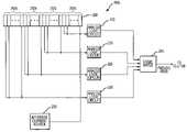
- FIG. 1illustrates a typical NAND flash memory array 10 of conventional design.
- the array 10is comprised of a large number of flash memory cells, collectively indicated by reference numeral 14 .
- the array of flash memory cells 14is typically divided into a number of blocks, one of which is shown in FIG. 1 . Each block includes a number of rows, which, in the example shown in FIG. 1 , includes 32 rows.
- the cells 14 in the same rowhave their control gates coupled to a common word select line 30 , each of which receives a respective word line signal WL 0 -WL 31 .
- the cells 14 in the same columnhaving their sources and drains connected to each other in series. Thus all of the memory cells 14 in the same column of each block are typically connected in series with each other.
- the drain of the upper flash memory cell 14 in the blockis coupled to a bit line 20 through a first select gate transistor 24 .
- the conductive state of the transistors 24 in each blockare controlled by a source gate SG(D) signal.
- Each of the bit lines 20output a respective bit line signal BL 1 -BLN indicative of the data bit stored in the respective column of the array 10 .
- the bit lines 20extend through multiple blocks to respective sense amplifiers (not shown).
- the source of the lower flash memory cell 14 in the blockis coupled to a source line 26 through a second select gate transistor 28 .
- the conductive state of the transistors 28 in each blockare controlled by a source gate SG(S) signal.
- the source line 26receives a signal SL having various magnitudes depending upon whether the memory cells 14 are being programmed, read or erased.
- a read operationis performed on a row-by-row basis.
- the source line 26is coupled to ground, and the select gate transistors 24 , 28 for that block are turned ON responsive to high SG(D) and SG(S) signals.
- the bit line 20 for each columnis precharged to the supply voltage V CC .
- a read voltageis applied to a word select line 30 for the selected row, thereby applying the read voltage to the control gates of all of the flash memory cells 14 in that row.
- the magnitude of the read voltageis sufficient to turn ON all flash memory cells 14 that do not have a charged floating gate, but insufficient to turn ON all cells that have a charged floating gate.
- a voltage having a higher magnitudeis applied to the word select lines 30 for all of the non-selected rows. This voltage is large enough to turn ON the flash memory cells 14 even if their floating gates are storing charge. As a result, the bit line 20 for each column will be low if the cell 14 in that column of the selected row is not storing charge. Otherwise the bit line 20 remains high at V CC .
- the voltage on each bit line 20is compared to a reference voltage by a respective sense amplifier (not shown). If the voltage on the bit line 20 is less than the reference voltage, the sense amplifier outputs a voltage corresponding to a “1” binary value of the read data bit. If the voltage on the bit line 20 is greater than the reference voltage, the sense amplifier outputs a voltage corresponding to a “0” binary value of the read data bit.
- the select gate transistors 28 shown in FIG. 1are NMOS transistors, which are normally fabricated in a p-well (not shown).
- the word select line 30 for the selected rowis coupled to ground, and the p-well is coupled to a positive voltage.
- the positive voltageis coupled through the PN junction formed by the p-well and the n-doped drain of the select gate transistors 28 to apply the positive voltage to the sources of the flash memory cells 14 .
- the positive voltagethen depletes charge from the floating gates in all of the cells 14 , thereby erasing all of the memory cells 14 in the selected row.
- the flash memory cells 14are normally erased on a block-by-block basis by grounding the word select lines 30 for all of the cells 14 in the block. Insofar as erasing the cells 14 removes charge from their floating gates, erasing the cells 14 effectively programs them to store logic “1” bit values.
- a programming voltageis applied to the word select line 30 for the selected row, and a voltage sufficient to turn ON the remaining cells 14 is applied to the control gates of the remaining flash memory cells 14 .
- the first column select transistor 24is turned ON and voltages corresponding to the data bits that are to be programmed are applied to the respective bit lines. If the voltage of a bit line 20 is at ground corresponding to a logic “0,” charge will be stored in the floating gate of the flash memory cell 14 in that column of the selected row. Otherwise, a voltage on the bit line 20 corresponding to a logic “1” prevents any charge from being stored on the floating gate. Programming is therefore performed on a row-by-row basis.
- the storage capacity of a flash memory arraycan be increased by storing multiple bits of data in each flash memory cell 14 . This can be accomplished by storing multiple levels of charge on the floating gate of each cell 14 .
- These memory devicesare commonly referred to as multi-bit or multi-level flash memory cells, known as “MLC memory cells.”
- MLC memory cellsmultiple bits of binary data corresponding to distinct threshold voltage levels defined over respective voltage ranges are stored within a single cell. Each distinct threshold voltage level corresponds to a respective combination of data bits. Specifically, the number N of bits requires 2 N distinct threshold voltage levels. For example, for a flash memory cell to store 2 bits of data, 4 distinct threshold voltage levels corresponding to bit states 00 , 01 , 10 , and 11 are needed.
- the threshold voltage level for which the memory cell 14 conducts currentcorresponds to a combination of bits representing data programmed into the cell.
- the two or more bits stored in each flash memory cell 14can be adjacent bits in the same page of data. However, more frequently, one bit is treated as a bit in one page of data, and the other bit is treated as the corresponding bit in an adjacent page of data.
- the bit states assigned to respective charge levelsare normally the same for all rows of memory cells in an array.
- the bit states assigned to the flash memory cells in the arrayare usually implemented in hardware and thus cannot be changed during operation of the flash memory device.
- a multi-level flash memory cellis programmed by applying a programming voltage to the control gate and holding the drain to a constant voltage over a proper time period to store enough charge in the floating gate to move the threshold voltage V t of the flash memory cell 14 to a desired level.
- This threshold voltage level V trepresents a bit state of the cell corresponding to the combination of data bits stored in the cell.
- programming of multi-level cellsis performed on a row-by-row basis.
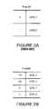
- FIG. 2Aillustrates the cell data map for a conventional one-bit-per-cell flash cell.
- two separate charge levels or rangesare defined within the overall flash cell threshold voltage V t range.
- V tthreshold voltage
- all that is necessaryis to determine whether the threshold voltage V t is above or below the midpoint between the two levels. Voltages in one level are interpreted as a single binary bit (zero or one) while voltages in the other level are interpreted as the complementary binary bit (one or zero).
- FIG. 2Billustrates the cell data map for a multi-level flash memory cell capable of storing two bits.
- the data mapdefines four separate charge ranges or levels (Levels 0 , 1 , 2 , and 3 ) within the range of the cell's overall maximum threshold voltage V t .
- Each levelis assigned a two-bit pair or bit-set 00 , 01 , 10 , or 11 .
- the bit setsare assigned for increasing levels of stored charge as 11 , 01 , 00 , 10 so that only a single bit changes with each incremental increase in stored charge.
- the multiple bits stored in each rowcan be used as adjacent bits in a single page of memory.
- the multiple bits stored in each rowcan be used as corresponding bits in two different pages of memory.
- the data bits X,Y stored in the first columncan be used so that X is the first data bit of one page, and Y is the first data bit of an adjacent page.
- the block containing the rowis normally tagged as being defective, and a redundant block is substituted for the defective block.
- Column-to-column shortsare normally repaired by substituting a redundant column of memory cells for each defective column.
- circuitrythere is also a limit to the precision with which circuitry can store an analog value on the floating gate of a flash cell, particularly where multiple levels of charge must be stored.
- the flash cells across an entire array and even across a single rowmay not all behave identically.
- conventional circuitry for programming or erasing the flash cellstypically perform these tasks in an iterative manner.
- the circuitryapplies a programming pulse having an appropriate duration and magnitude to a word select line 30 .
- the pulseis applied to the control gate of each of the cells 14 to charge the floating gate to target levels corresponding to bit state values to which the cells are to be programmed.
- the cellsare then interrogated to verify that the floating gate of each cell has been charged to that level.
- the circuitryagain applies a programming pulse to the control gate of each of the cells, and the cells are again verified. This process is repeated until the floating gates have been charged to the target levels. As can be appreciated, it can require a considerable period of time to program flash memory cells in this iterative manner. Additionally, each time the programming pulse is applied to a word select line 30 , the pulse can inadvertently couple charge to floating gates of the programmed memory cells 14 in the corresponding row or an adjacent row. This problem is particularly acute for multi-level flash memory cells.
- One approach to preventing an excessive number of programming pulses from being applied to a rowis to simply consider the row to be properly programmed when the proper programming of less than all of the memory cells in the row have been verified. Using this technique, a “pseudo pass” condition is considered to exist even though one or more of the memory cells are programmed to erroneous bit states. These bit state errors can be corrected when the row is read using the conventional ECC techniques described above. However, these conventional ECC techniques are usually limited to repairing a relatively small number of data bit errors in each row.
- the number of data bit errors existing after one or a few programming pulses have been applied to a rowcan exceed the number of data bit errors that can be corrected by ECC circuitry.
- FIG. 1is a schematic diagram showing a conventional NAND array of flash memory cells.
- FIGS. 2A and 2Bare schematic diagrams illustrating the manner in which the flash cells shown in FIG. 1 are programmed to store one or more data bits.
- FIG. 3is a block diagram showing a flash memory device that may be used according to one example of the invention.
- FIG. 4is a block diagram of one example of a conventional pseudo pass detector that has been used in the flash memory device of FIG. 3 .
- FIG. 5is a block diagram of a pseudo pass detector according to one example of the invention that may be used in the flash memory device of FIG. 3 .
- FIG. 6is a block diagram of a pseudo pass detector according to another example of the invention that may be used in the flash memory device of FIG. 3 .
- FIG. 7is a simplified block diagram of a processor-based system including the flash memory device of FIG. 3 or another flash memory device using a pseudo pass detector according to an example of the invention.
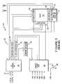
- FIG. 3A flash memory device 100 of conventional design that can be used according to one example of the invention is shown in FIG. 3 .
- the flash memory device 100includes an array 130 of flash memory cells arranged in banks of rows and columns.
- the flash memory cells in the array 130have their control gates coupled to word select lines, drain regions coupled to local bit lines, and source regions selectively coupled to a ground potential as shown in FIG. 1 .
- command, address and write data signalsare not applied to the flash memory device 100 through respective command, address and data buses. Instead, most command signals, the address signals and the write data signals are applied to the memory device 100 as sets of sequential input/output (“I/O”) signals transmitted through an I/O bus 134 . Similarly, read data signals are output from the flash memory device 100 through the I/O bus 134 .
- the I/O busis connected to an I/O control unit 140 that routes the signals between the I/O bus 134 and an internal data bus 142 , an address register 144 , a command register 146 and a status register 148 .
- the flash memory device 100also includes a control logic unit 150 that receives a number of control signals, including an active low chip enable signal CE#, a command latch enable signal CLE, an address latch enable signal ALE, an active low write enable signal WE#, an active low read enable signal RE#, and an active low write protect WP# signal.
- a control logic unit 150receives a number of control signals, including an active low chip enable signal CE#, a command latch enable signal CLE, an address latch enable signal ALE, an active low write enable signal WE#, an active low read enable signal RE#, and an active low write protect WP# signal.
- the chip enable signal CE#is active low
- command, address and data signalsmay be transferred between the memory device 100 and a memory access device (not shown).
- the control logic unit 150causes the I/O control unit 140 to route signals received through the I/O bus 134 to the command register 146 responsive to the rising edge of the WE# signal.
- the I/O control unit 140routes signals received through the I/O bus 134 to the address register 146 responsive to the rising edge of the WE# signal.
- the write enable signal WE#is also used to gate write data signals from the memory access device (not shown) to the memory device 100
- the read enable signal RE#is used to gate the read data signals from the memory device 100 to the memory access device (not shown).
- the I/O control unit 140transfers the write data signals and read data signals between the I/O bus 134 and the internal data bus 142 when the CLE and ALE signals are both low.
- an active low write protect signal WP#prevents the memory device 100 from inadvertently performing programming or erase functions.
- the control logic unit 150is also coupled to the internal data bus 142 to receive write date from the I/O control unit for reasons that will be explained below.
- the status register 148can be read responsive to a read status command. After the read status command, all subsequent read commands will result in status data being read from the status register 148 until a subsequent read status command is received.
- the status data read from the status register 148provides information about the operation of the memory device 100 , such as whether programming and erase operations were completed without error.
- the address register 146stores row and column address signals applied to the memory device 100 .
- the address register 146then outputs the row address signals to a row decoder 160 and the column address signals to a column decoder 164 .
- the row decoder 160asserts word select lines 30 ( FIG. 1 ) corresponding to the decoded row address signals.
- the column decoder 164enables write data signals to be applied to bit lines for columns corresponding to the column address signals and allow read data signals to be coupled from bit lines for columns corresponding to the column address signals.
- the flash memory cells in the array 130are erased, programmed, or read.
- the memory array 130is programmed on a row-by-row or page-by-page basis.
- the I/O control unit 140routes write data signals to a cache register 170 .
- the write data signalsare stored in the cache register 170 in successive sets each having a size corresponding to the width of the I/O bus 134 .
- the cache register 170sequentially stores the sets of write data signals for an entire row or page of flash memory cells in the array 130 .
- All of the stored write data signalsare then used to program a row or page of memory cells in the array 130 selected by the row address stored in the address register 146 .
- data signals from a row or page of memory cells selected by the row address stored in the address register 146are stored in a data register 180 .
- Sets of data signals corresponding in size to the width of the I/O bus 134are then sequentially transferred through the I/O control unit 140 from the data register 180 to the I/O bus 134 .
- the array 130is typically read on a row-by-row or page-by-page basis, a selected portion of a selected row or page may be read by specifying a corresponding column address.
- the flash memory device 130also includes an NMOS transistor 186 having its gate coupled to receive a signal from the control logic unit 150 .
- the control logic unit 150When the memory device 100 is busy processing a programming, erase or read command, the control logic unit 150 outputs a high signal to cause the transistor 186 to output an active low read/busy signal R/B#. At other times, the transistor 186 is turned OFF to indicate to a memory access device that the device 100 is able to accept and process memory commands.
- the control logic unit 150causes the write data signals stored in the cache register 170 to program a row or page of memory cells in the array 130 . As also explained above, this is accomplished in an iterative manner in which the control logic unit 150 repetitively performs program and verify operations.
- the cache register 170includes a pseudo pass detector 190 .
- the pseudo pass detector 190outputs a signal to the control logic unit 150 when a sufficient number of cells have been programmed that programming of the row or page can be considered complete.
- a pseudo pass detector 190 a of conventional designis shown in FIG. 4 .
- the detector 190 aincludes a comparator 200 having a plurality of comparator stages, one of which is provided for each data signal stored in the cache register 170 .
- One of the inputs of each stagereceives a respective one of the data signals stored in the cache register 170
- the other input of the stagereceives a corresponding data signal read from a row of memory cells during verification.
- the respective stages of the comparator 200thus compare each read data signal stored in the cache register 170 to the data signal stored in a corresponding memory cell in the row being programmed to determine if the cell has been properly programmed.
- the corresponding stage of the comparator 200If the data signal stored in a memory cell does not match the corresponding read data signal stored in the cache register 170 , the corresponding stage of the comparator 200 outputs a current signal that draws a predetermined amount of current from a common output line 202 . If a stage of the comparator 200 determines there is a match, it does not output a current signal but instead leaves its output isolated or tri-stated.
- the current signals from all of the stages of the comparator 200are applied through the common line 202 to an analog logic circuit 204 .
- the analog logic circuit 204generate a pseudo pass bit indicative of whether or not the number of improperly programmed memory cells exceed a predetermined number.
- the analog logic circuit 204performs this function by outputting a pseudo pass bit having one binary value if the total current drawn by all the current signals from the respective stages of the comparator 200 do not exceed a predetermined value, and a different binary value if the total current drawn exceeds the predetermined value.
- the analog logic circuit 204may be implemented, for example, by biasing a node high through a fixed resistance and detecting when the total current draw from the comparators 200 is sufficient to pull the voltage of the node below a predetermined threshold voltage.
- the analog logic circuit 204outputs a low pseudo pass bit to the control logic unit 150 as long as the number of improperly programmed memory cells is less than 5, i.e., 4.
- the control logic unit 150terminates, repetitively programming and verifying the data being stored in the row of memory cells being programmed.
- the 4 or fewer erroneous data signalscan then be corrected by conventional ECC circuitry (not shown) in the memory device 100 or in a flash memory controller (not shown) connected to the memory device 100 .
- the analog logic circuit 204outputs a high pseudo pass bit.
- the control logic unit 150can then continue to repetitively program and verify the data being stored in the row of memory cells being programmed.
- the conventional pseudo pass detector 190 auses an analog logic circuit 204 rather than a set of logic gates because the large number of signals that it receives, typically in the thousands, would require a large number of logic gates. The required number of logic gates would consume a great deal of space on an integrated circuit chip, and might draw a significant amount of power.
- the analog logic circuit 204can be implemented with significantly less circuitry and draw significantly less power. However, the logic function performed by the analog logic circuit 204 can easily be implemented by digital means in a manner that will be apparent to one skilled in the art.
- the conventional pseudo pass detector 190 a shown in FIG. 4may cause the control logic unit 150 to perform more program and verify operations than are actually necessary to reduce the number of data errors to a level that can be corrected by ECC circuitry. More specifically, the data stored in the memory array 130 are often read from the memory device 100 in sets of 512 bytes, which correspond to a sector of a hard disk drive. However, regardless of whether this is the case, the data will be read from the memory device in sets that are smaller than the number of data signals stored in each row or page of memory cells in the array 130 . For example, if the rows in the array 130 store 2048 data signals, the data will be read from the row in four sets of 512 bytes.
- the maximum number of erroneous bits read from the rowwill always be 4 or fewer, and these can be corrected by the ECC circuitry.
- the ECC circuitrycould correct more than 4 erroneous data bits stored in a row or page. For example, if there are 3 erroneous bits in each of the sets of 512 bytes, the ECC circuitry would receive a maximum of 3 erroneous data bits from any one set. Therefore, the ECC circuitry could easily correct these bits even though there would be a total of 12 erroneous bits in the entire row or page.
- control logic unit 150would unnecessarily continue to perform program and verify operations until the total number of erroneous bit errors was reduced to 4. These unnecessary program and verify operations could corrupt the data stored in previously programmed cells for the reasons previously explained.
- the number of bit errorswas not limited to 4, and there were just 6 bit errors present in the same set of 512 bytes, these bits could not be corrected by the ECC circuitry since it would simultaneously receive more than 4 erroneous bits.
- program and verify operationsmust be performed to reduce the number of erroneous bits to 4 or less, even though doing so is sometimes unnecessary.
- a memory device 100 using the conventional pseudo pass detector 190 amay require more time than actually needed to program a row or page. Additionally, because of data corruption caused by an excessive number of programming pulses, the data stored in a row may become corrupted to the extent that they could not be corrected by ECC circuitry.
- a pseudo pass detector 190 bis shown in FIG. 5 .
- the pseudo pass detector 190 bdiffers from the conventional pseudo pass detector 190 a by performing its comparison operations on subsets of data signals stored in the cache register 170 .
- the number of data signals in each subsetis equal to the number of read data signals in each set output from the memory device 100 .
- the pseudo pass detector 190 bincludes the same comparator 200 that is used in the pseudo pass detector 190 a of FIG. 1 . However, the match signals from groups 202 a - d of stages of the comparator 200 are processed separately. In the example shown in FIG.
- the stages of the comparator 200are divided into 4 groups, 202 a - d , each of which contains 512 stages.
- the current signals from the stages in each groupare applied to respective analog logic circuits 220 .
- the analog logic circuits 220each compare the current drawn by the stages of the comparator 200 to which it is coupled to a current reference signal generated by a bit error current source 230 .
- the bit error current source 230generates a current corresponding to the maximum number of data errors that are considered acceptable in the corresponding subset of data signals.
- the same bit error current source 230may be used for all of the signal groups 202 a - d , as shown in FIG.
- a respective bit error current source 230may be provided for each group of stages, 202 a - d , of the comparator 200 .
- the comparator 200 and analog logic circuits 220 for each group 202 a - doperate in essentially the same manner as the comparator 200 and analog logic circuit 204 except that the current to which the currents drawn by the comparator stages is generated by the bit error current source.
- Each analog logic circuit 220outputs a respective pass signal whenever the number of errors in the data bits from the corresponding group of comparator stages is within the number of data errors that can be corrected by ECC circuitry (not shown). These pass signals from all of the analog logic circuits 220 are applied to logic gates 240 .
- the logic gates 240output a pseudo pass signal to the control logic unit 150 whenever all of the analog logic circuits 220 224 are outputting respective pass signals. Therefore, the control logic unit 150 will continue to perform program and verify operations until the number of errors in each set of data signals is within the number that can be corrected by ECC circuitry. However, the total number of errors in the data stored in an entire row or page can be well in excess of the number of errors that can be corrected by ECC circuitry.
- each row of cells in the arraystores 2048 bytes of data, and the data bytes are transferred from the memory device 100 in sets of 512 bytes. These data bytes are transferred to a flash memory controller (not shown) that can correct 4 or fewer data bit errors.
- the current output from the bit error current source 230thus corresponds to 4 bit errors.
- a pseudo pass detector 190 cis shown in FIG. 6 .
- the pseudo pass detector 190 cdiffers from the pseudo pass detector 190 b and conventional pseudo pass detector 190 a by performing its comparison operations digitally rather than by analog means.
- the pseudo pass detector 190 bincludes a comparator 250 that outputs a digital match signal from each stage if the data signal stored in a corresponding memory cell matches the corresponding read data signal stored in the cache register 170 .
- the stages of the comparator 250are divided into 4 groups, 252 a - d , each of which contains 512 stages.
- the match signals from the stages in each groupare applied to respective logic gates 270 that generate a plurality of bits specifying the number of data errors in the corresponding subset of data signals. These bits are applied to a respective comparator 274 that compares the number to a number indicated by bits from a bit error register 280 .
- the same bit error register 280may be used for all of the signal groups 252 a - d , as shown in FIG. 6 , or a respective bit error register 280 may be provided for each group of stages, 252 a - d , of the comparator 250 .
- Each comparator 274outputs a respective pass signal whenever the number of errors in the data bits from the corresponding group of stages is within the number of data errors that can be corrected by ECC circuitry (not shown).
- the pseudo pass detector 190 calso includes a set of logic gates 290 that receive the pass signals from the comparator 274 for each group of stages of the comparator 250 .
- the logic gates 290output a pseudo pass signal to the control logic unit 150 whenever all of the comparators 274 are outputting respective pass signals. Therefore, the control logic unit 150 will continue to perform program and verify operations until the number of errors in each set of data signals is within the number that can be corrected by ECC circuitry.
- the total number of errors in the data stored in an entire row or pagecan be well in excess of the number of errors that can be corrected by ECC circuitry.
- each row of cells in the arraystores 2048 bytes of data, and the data bytes are transferred from the memory device 100 in sets of 512 bytes. These data bytes are transferred to a flash memory controller (not shown) that can correct 4 or fewer data bit errors. The number 4 is therefore stored in the bit error register 280 .
- FIG. 7is a block diagram of a processor-based system 300 including processor circuitry 302 having volatile memory 310 .
- the processor circuitry 302is coupled through address, data, and control buses to the volatile memory 310 to provide for writing data to and reading data from the volatile memory 310 .
- the processor circuitry 302includes circuitry for performing various processing functions, such as executing specific software to perform specific calculations or tasks.
- the processor-based system 300also includes one or more input devices 304 coupled to the processor circuitry 302 to allow an operator to interface with the processor-based system 300 . Examples of input devices 304 include keypads, touch screens, and scroll wheels.
- the processor-based system 300also includes one or more output devices 306 coupled to the processor circuitry 302 to provide output information to the operator.
- the output device 306is a visual display providing visual information to the operator.
- Data storage 308is also coupled to the processor circuitry 302 through a controller 320 to store data that is to be retained even when power is not supplied to the processor-based system 300 or to the data storage 308 .
- the flash memory device 100or a flash memory device according to some other example of the invention, can be used for the data storage 308 , and a flash memory controller can be used for the controller 320 .
- the controller 320includes ECC circuitry 324 for correcting errors in data read from the flash memory device used for the data storage 308 , as previously explained.
Landscapes
- Engineering & Computer Science (AREA)
- Microelectronics & Electronic Packaging (AREA)
- Read Only Memory (AREA)
Abstract
Description
Claims (35)
Priority Applications (4)
| Application Number | Priority Date | Filing Date | Title |
|---|---|---|---|
| US11/506,375US7567461B2 (en) | 2006-08-18 | 2006-08-18 | Method and system for minimizing number of programming pulses used to program rows of non-volatile memory cells |
| US12/505,886US7961522B2 (en) | 2006-08-18 | 2009-07-20 | Method and system for minimizing number of programming pulses used to program rows of non-volatile memory cells |
| US13/113,853US8730737B2 (en) | 2006-08-18 | 2011-05-23 | Method and system for minimizing number of programming pulses used to program rows of non-volatile memory cells |
| US14/281,694US9019774B2 (en) | 2006-08-18 | 2014-05-19 | Method and system for minimizing number of programming pulses used to program rows of non-volatile memory cells |
Applications Claiming Priority (1)
| Application Number | Priority Date | Filing Date | Title |
|---|---|---|---|
| US11/506,375US7567461B2 (en) | 2006-08-18 | 2006-08-18 | Method and system for minimizing number of programming pulses used to program rows of non-volatile memory cells |
Related Child Applications (1)
| Application Number | Title | Priority Date | Filing Date |
|---|---|---|---|
| US12/505,886DivisionUS7961522B2 (en) | 2006-08-18 | 2009-07-20 | Method and system for minimizing number of programming pulses used to program rows of non-volatile memory cells |
Publications (2)
| Publication Number | Publication Date |
|---|---|
| US20080043535A1 US20080043535A1 (en) | 2008-02-21 |
| US7567461B2true US7567461B2 (en) | 2009-07-28 |
Family
ID=39101232
Family Applications (4)
| Application Number | Title | Priority Date | Filing Date |
|---|---|---|---|
| US11/506,375Active2027-06-05US7567461B2 (en) | 2006-08-18 | 2006-08-18 | Method and system for minimizing number of programming pulses used to program rows of non-volatile memory cells |
| US12/505,886Active2026-10-27US7961522B2 (en) | 2006-08-18 | 2009-07-20 | Method and system for minimizing number of programming pulses used to program rows of non-volatile memory cells |
| US13/113,853Active2027-03-11US8730737B2 (en) | 2006-08-18 | 2011-05-23 | Method and system for minimizing number of programming pulses used to program rows of non-volatile memory cells |
| US14/281,694ActiveUS9019774B2 (en) | 2006-08-18 | 2014-05-19 | Method and system for minimizing number of programming pulses used to program rows of non-volatile memory cells |
Family Applications After (3)
| Application Number | Title | Priority Date | Filing Date |
|---|---|---|---|
| US12/505,886Active2026-10-27US7961522B2 (en) | 2006-08-18 | 2009-07-20 | Method and system for minimizing number of programming pulses used to program rows of non-volatile memory cells |
| US13/113,853Active2027-03-11US8730737B2 (en) | 2006-08-18 | 2011-05-23 | Method and system for minimizing number of programming pulses used to program rows of non-volatile memory cells |
| US14/281,694ActiveUS9019774B2 (en) | 2006-08-18 | 2014-05-19 | Method and system for minimizing number of programming pulses used to program rows of non-volatile memory cells |
Country Status (1)
| Country | Link |
|---|---|
| US (4) | US7567461B2 (en) |
Cited By (8)
| Publication number | Priority date | Publication date | Assignee | Title |
|---|---|---|---|---|
| US20070115743A1 (en)* | 2005-09-09 | 2007-05-24 | Stmicroelectronics S.R.I. | Memory architecture with serial peripheral interface |
| US20080304317A1 (en)* | 2007-06-05 | 2008-12-11 | Roohparvar Frankie F | Solid state memory utilizing analog communication of data values |
| US20090044085A1 (en)* | 2007-08-06 | 2009-02-12 | Industrial Technology Research Institute | Defect management method for storage medium and system thereof |
| US20090141602A1 (en)* | 2007-11-29 | 2009-06-04 | Industrial Technology Research Institute | Recording medium structure capable of displaying defect rate |
| US20100162084A1 (en)* | 2008-12-18 | 2010-06-24 | Richard Coulson | Data error recovery in non-volatile memory |
| US20110141832A1 (en)* | 2009-12-15 | 2011-06-16 | Gopinath Balakrishnan | Program cycle skip |
| US20140164682A1 (en)* | 2012-12-12 | 2014-06-12 | SK Hynix Inc. | Nonvolatile memory apparatus, operating method thereof, and data processing system having the same |
| US20190130991A1 (en)* | 2017-11-02 | 2019-05-02 | Samsung Electronics Co., Ltd. | Semiconductor memory devices, memory systems and methods of operating semiconductor memory devices |
Families Citing this family (74)
| Publication number | Priority date | Publication date | Assignee | Title |
|---|---|---|---|---|
| WO2007132453A2 (en) | 2006-05-12 | 2007-11-22 | Anobit Technologies Ltd. | Distortion estimation and cancellation in memory devices |
| WO2007132452A2 (en)* | 2006-05-12 | 2007-11-22 | Anobit Technologies | Reducing programming error in memory devices |
| WO2007132456A2 (en)* | 2006-05-12 | 2007-11-22 | Anobit Technologies Ltd. | Memory device with adaptive capacity |
| KR101202537B1 (en)* | 2006-05-12 | 2012-11-19 | 애플 인크. | Combined distortion estimation and error correction coding for memory devices |
| US20080123405A1 (en)* | 2006-08-18 | 2008-05-29 | Mammen Thomas | Implanted multi-bit NAND ROM |
| WO2008026203A2 (en) | 2006-08-27 | 2008-03-06 | Anobit Technologies | Estimation of non-linear distortion in memory devices |
| WO2008053473A2 (en) | 2006-10-30 | 2008-05-08 | Anobit Technologies Ltd. | Memory cell readout using successive approximation |
| US7975192B2 (en)* | 2006-10-30 | 2011-07-05 | Anobit Technologies Ltd. | Reading memory cells using multiple thresholds |
| US7924648B2 (en) | 2006-11-28 | 2011-04-12 | Anobit Technologies Ltd. | Memory power and performance management |
| WO2008068747A2 (en)* | 2006-12-03 | 2008-06-12 | Anobit Technologies Ltd. | Automatic defect management in memory devices |
| US7593263B2 (en)* | 2006-12-17 | 2009-09-22 | Anobit Technologies Ltd. | Memory device with reduced reading latency |
| US7900102B2 (en)* | 2006-12-17 | 2011-03-01 | Anobit Technologies Ltd. | High-speed programming of memory devices |
| US7751240B2 (en)* | 2007-01-24 | 2010-07-06 | Anobit Technologies Ltd. | Memory device with negative thresholds |
| US8151166B2 (en)* | 2007-01-24 | 2012-04-03 | Anobit Technologies Ltd. | Reduction of back pattern dependency effects in memory devices |
| US8369141B2 (en)* | 2007-03-12 | 2013-02-05 | Apple Inc. | Adaptive estimation of memory cell read thresholds |
| US8001320B2 (en)* | 2007-04-22 | 2011-08-16 | Anobit Technologies Ltd. | Command interface for memory devices |
| WO2008139441A2 (en) | 2007-05-12 | 2008-11-20 | Anobit Technologies Ltd. | Memory device with internal signal processing unit |
| US8234545B2 (en)* | 2007-05-12 | 2012-07-31 | Apple Inc. | Data storage with incremental redundancy |
| US7925936B1 (en) | 2007-07-13 | 2011-04-12 | Anobit Technologies Ltd. | Memory device with non-uniform programming levels |
| US8259497B2 (en) | 2007-08-06 | 2012-09-04 | Apple Inc. | Programming schemes for multi-level analog memory cells |
| US8174905B2 (en)* | 2007-09-19 | 2012-05-08 | Anobit Technologies Ltd. | Programming orders for reducing distortion in arrays of multi-level analog memory cells |
| US7773413B2 (en) | 2007-10-08 | 2010-08-10 | Anobit Technologies Ltd. | Reliable data storage in analog memory cells in the presence of temperature variations |
| US8527819B2 (en)* | 2007-10-19 | 2013-09-03 | Apple Inc. | Data storage in analog memory cell arrays having erase failures |
| US8000141B1 (en) | 2007-10-19 | 2011-08-16 | Anobit Technologies Ltd. | Compensation for voltage drifts in analog memory cells |
| US8068360B2 (en)* | 2007-10-19 | 2011-11-29 | Anobit Technologies Ltd. | Reading analog memory cells using built-in multi-threshold commands |
| US8270246B2 (en)* | 2007-11-13 | 2012-09-18 | Apple Inc. | Optimized selection of memory chips in multi-chips memory devices |
| US8225181B2 (en) | 2007-11-30 | 2012-07-17 | Apple Inc. | Efficient re-read operations from memory devices |
| US8209588B2 (en)* | 2007-12-12 | 2012-06-26 | Anobit Technologies Ltd. | Efficient interference cancellation in analog memory cell arrays |
| US8456905B2 (en) | 2007-12-16 | 2013-06-04 | Apple Inc. | Efficient data storage in multi-plane memory devices |
| US8085586B2 (en)* | 2007-12-27 | 2011-12-27 | Anobit Technologies Ltd. | Wear level estimation in analog memory cells |
| US8156398B2 (en)* | 2008-02-05 | 2012-04-10 | Anobit Technologies Ltd. | Parameter estimation based on error correction code parity check equations |
| US7924587B2 (en)* | 2008-02-21 | 2011-04-12 | Anobit Technologies Ltd. | Programming of analog memory cells using a single programming pulse per state transition |
| US7864573B2 (en) | 2008-02-24 | 2011-01-04 | Anobit Technologies Ltd. | Programming analog memory cells for reduced variance after retention |
| US8230300B2 (en)* | 2008-03-07 | 2012-07-24 | Apple Inc. | Efficient readout from analog memory cells using data compression |
| US8059457B2 (en) | 2008-03-18 | 2011-11-15 | Anobit Technologies Ltd. | Memory device with multiple-accuracy read commands |
| US8400858B2 (en) | 2008-03-18 | 2013-03-19 | Apple Inc. | Memory device with reduced sense time readout |
| US8498151B1 (en) | 2008-08-05 | 2013-07-30 | Apple Inc. | Data storage in analog memory cells using modified pass voltages |
| US7924613B1 (en) | 2008-08-05 | 2011-04-12 | Anobit Technologies Ltd. | Data storage in analog memory cells with protection against programming interruption |
| US8169825B1 (en) | 2008-09-02 | 2012-05-01 | Anobit Technologies Ltd. | Reliable data storage in analog memory cells subjected to long retention periods |
| US8949684B1 (en) | 2008-09-02 | 2015-02-03 | Apple Inc. | Segmented data storage |
| US8000135B1 (en) | 2008-09-14 | 2011-08-16 | Anobit Technologies Ltd. | Estimation of memory cell read thresholds by sampling inside programming level distribution intervals |
| US8482978B1 (en) | 2008-09-14 | 2013-07-09 | Apple Inc. | Estimation of memory cell read thresholds by sampling inside programming level distribution intervals |
| US8239734B1 (en) | 2008-10-15 | 2012-08-07 | Apple Inc. | Efficient data storage in storage device arrays |
| US8713330B1 (en) | 2008-10-30 | 2014-04-29 | Apple Inc. | Data scrambling in memory devices |
| US8208304B2 (en)* | 2008-11-16 | 2012-06-26 | Anobit Technologies Ltd. | Storage at M bits/cell density in N bits/cell analog memory cell devices, M>N |
| US8248831B2 (en)* | 2008-12-31 | 2012-08-21 | Apple Inc. | Rejuvenation of analog memory cells |
| US8174857B1 (en) | 2008-12-31 | 2012-05-08 | Anobit Technologies Ltd. | Efficient readout schemes for analog memory cell devices using multiple read threshold sets |
| US8924661B1 (en) | 2009-01-18 | 2014-12-30 | Apple Inc. | Memory system including a controller and processors associated with memory devices |
| US8228701B2 (en) | 2009-03-01 | 2012-07-24 | Apple Inc. | Selective activation of programming schemes in analog memory cell arrays |
| US8832354B2 (en)* | 2009-03-25 | 2014-09-09 | Apple Inc. | Use of host system resources by memory controller |
| US8259506B1 (en) | 2009-03-25 | 2012-09-04 | Apple Inc. | Database of memory read thresholds |
| US8238157B1 (en) | 2009-04-12 | 2012-08-07 | Apple Inc. | Selective re-programming of analog memory cells |
| US8479080B1 (en) | 2009-07-12 | 2013-07-02 | Apple Inc. | Adaptive over-provisioning in memory systems |
| US8495465B1 (en) | 2009-10-15 | 2013-07-23 | Apple Inc. | Error correction coding over multiple memory pages |
| US8677054B1 (en) | 2009-12-16 | 2014-03-18 | Apple Inc. | Memory management schemes for non-volatile memory devices |
| US8437183B2 (en)* | 2009-12-16 | 2013-05-07 | Sandisk Il Ltd. | Auxiliary parity bits for data written in multi-level cells |
| US8694814B1 (en) | 2010-01-10 | 2014-04-08 | Apple Inc. | Reuse of host hibernation storage space by memory controller |
| US8572311B1 (en) | 2010-01-11 | 2013-10-29 | Apple Inc. | Redundant data storage in multi-die memory systems |
| US8694853B1 (en) | 2010-05-04 | 2014-04-08 | Apple Inc. | Read commands for reading interfering memory cells |
| US8572423B1 (en) | 2010-06-22 | 2013-10-29 | Apple Inc. | Reducing peak current in memory systems |
| US8595591B1 (en) | 2010-07-11 | 2013-11-26 | Apple Inc. | Interference-aware assignment of programming levels in analog memory cells |
| US9104580B1 (en) | 2010-07-27 | 2015-08-11 | Apple Inc. | Cache memory for hybrid disk drives |
| US8645794B1 (en) | 2010-07-31 | 2014-02-04 | Apple Inc. | Data storage in analog memory cells using a non-integer number of bits per cell |
| US8856475B1 (en) | 2010-08-01 | 2014-10-07 | Apple Inc. | Efficient selection of memory blocks for compaction |
| US8694854B1 (en) | 2010-08-17 | 2014-04-08 | Apple Inc. | Read threshold setting based on soft readout statistics |
| US9021181B1 (en) | 2010-09-27 | 2015-04-28 | Apple Inc. | Memory management for unifying memory cell conditions by using maximum time intervals |
| US8634241B2 (en)* | 2010-12-13 | 2014-01-21 | Aplus Flash Technology, Inc. | Universal timing waveforms sets to improve random access read and write speed of memories |
| KR101212739B1 (en)* | 2010-12-21 | 2012-12-14 | 에스케이하이닉스 주식회사 | Non-volatile memory device and cache program method of the same |
| KR102470606B1 (en) | 2015-11-26 | 2022-11-28 | 삼성전자주식회사 | Nonvolatile memory device and storage device including nonvolatile memory device |
| CN114400041A (en)* | 2021-03-15 | 2022-04-26 | 长江存储科技有限责任公司 | Verification error bit quantization circuit and method for semiconductor memory |
| US11556416B2 (en) | 2021-05-05 | 2023-01-17 | Apple Inc. | Controlling memory readout reliability and throughput by adjusting distance between read thresholds |
| US11847342B2 (en) | 2021-07-28 | 2023-12-19 | Apple Inc. | Efficient transfer of hard data and confidence levels in reading a nonvolatile memory |
| US11908523B2 (en)* | 2021-09-01 | 2024-02-20 | Micron Technology, Inc. | Express programming using advanced cache register release in a memory sub-system |
| CN114242142A (en)* | 2021-12-08 | 2022-03-25 | 上海集成电路装备材料产业创新中心有限公司 | Programming device, method and novel memory |
Citations (51)
| Publication number | Priority date | Publication date | Assignee | Title |
|---|---|---|---|---|
| US4498151A (en) | 1980-04-17 | 1985-02-05 | Texas Instruments Incorporated | On board non-volatile memory programming |
| US5023613A (en) | 1988-03-31 | 1991-06-11 | Harris Semiconductor Patents, Inc. | Decoder error prevention apparatus for use in flash analog-to-digital converters |
| US5142541A (en) | 1988-12-15 | 1992-08-25 | Samsung Electronics Co., Ltd. | Error-bit generating circuit for use in a non-volatile semiconductor memory device |
| US5252974A (en) | 1986-12-24 | 1993-10-12 | Zdzislaw Gulczynski | Encoder with error correction particularly for flash analog-to-digital converters |
| US5268870A (en) | 1988-06-08 | 1993-12-07 | Eliyahou Harari | Flash EEPROM system and intelligent programming and erasing methods therefor |
| US5377145A (en) | 1991-02-11 | 1994-12-27 | Intel Corporation | Circuitry and method for programming and erasing a non-volatile semiconductor memory |
| US5475693A (en) | 1994-12-27 | 1995-12-12 | Intel Corporation | Error management processes for flash EEPROM memory arrays |
| US5513144A (en) | 1995-02-13 | 1996-04-30 | Micron Technology, Inc. | On-chip memory redundancy circuitry for programmable non-volatile memories, and methods for programming same |
| US5523972A (en) | 1994-06-02 | 1996-06-04 | Intel Corporation | Method and apparatus for verifying the programming of multi-level flash EEPROM memory |
| US5587946A (en) | 1993-03-18 | 1996-12-24 | Sgs-Thomson Microelectronics S.R.L. | Method of reading, erasing and programming a nonvolatile flash-EEPROM memory arrray using source line switching transistors |
| US5621738A (en) | 1991-12-10 | 1997-04-15 | Eastman Kodak Company | Method for programming flash EEPROM devices |
| US5727003A (en) | 1995-07-03 | 1998-03-10 | Cirrus Logic, Inc. | Method and apparatus for flash burst error correction |
| US5751637A (en) | 1995-06-07 | 1998-05-12 | Macronix International Co., Ltd. | Automatic programming algorithm for page mode flash memory with variable programming pulse height and pulse width |
| US5754567A (en) | 1996-10-15 | 1998-05-19 | Micron Quantum Devices, Inc. | Write reduction in flash memory systems through ECC usage |
| US5765185A (en) | 1995-03-17 | 1998-06-09 | Atmel Corporation | EEPROM array with flash-like core having ECC or a write cache or interruptible load cycles |
| US5828862A (en) | 1994-05-04 | 1998-10-27 | International Business Machines Corporation | Game programming flash memory cartridge system including a programmer and a reprogrammable cartridge |
| US5881295A (en) | 1995-02-07 | 1999-03-09 | Hitachi, Ltd. | Data processor which controls interrupts during programming and erasing of on-chip erasable and programmable non-volatile program memory |
| US5909449A (en) | 1997-09-08 | 1999-06-01 | Invox Technology | Multibit-per-cell non-volatile memory with error detection and correction |
| US5925140A (en) | 1993-04-30 | 1999-07-20 | Intel Corporation | Apparatus and method for error free loading of a programmable non-volatile memory over a datalink |
| US5966723A (en) | 1997-05-16 | 1999-10-12 | Intel Corporation | Serial programming mode for non-volatile memory |
| US5991517A (en) | 1989-04-13 | 1999-11-23 | Sandisk Corporation | Flash EEprom system with cell by cell programming verification |
| US6216251B1 (en) | 1999-04-30 | 2001-04-10 | Motorola Inc | On-chip error detection and correction system for an embedded non-volatile memory array and method of operation |
| US6247168B1 (en) | 1997-04-29 | 2001-06-12 | Rockwell Technologies, Llc | Embedded non-volatile programming tool |
| US6317371B2 (en) | 1996-02-29 | 2001-11-13 | Hitachi, Ltd. | Storage device with an error correction unit and an improved arrangement for accessing and transferring blocks of data stored in a non-volatile semiconductor memory |
| US6421757B1 (en) | 1998-09-30 | 2002-07-16 | Conexant Systems, Inc | Method and apparatus for controlling the programming and erasing of flash memory |
| US6426893B1 (en) | 2000-02-17 | 2002-07-30 | Sandisk Corporation | Flash eeprom system with simultaneous multiple data sector programming and storage of physical block characteristics in other designated blocks |
| US6438726B1 (en) | 1999-05-18 | 2002-08-20 | Advanced Micro Devices, Inc. | Method of dual use of non-volatile memory for error correction |
| US6490201B2 (en) | 2000-09-28 | 2002-12-03 | Hitachi, Ltd. | Non-volatile memory and method of non-volatile memory programming |
| US6498749B1 (en) | 1999-11-01 | 2002-12-24 | Koninklijke Philips Electronics N.V. | Data processing circuit with non-volatile memory and error correction circuitry |
| US6687158B2 (en) | 2001-12-21 | 2004-02-03 | Fujitsu Limited | Gapless programming for a NAND type flash memory |
| US6728164B2 (en) | 2001-09-26 | 2004-04-27 | Kabushiki Kaisha Toshiba | Flash memory rewrite circuit, semiconductor integrated circuit, memory card having the semiconductor integrated circuit thereof, method of rewriting flash memory and flash memory rewriting program |
| US6754103B2 (en) | 2002-11-04 | 2004-06-22 | Silicon Storage Technology, Inc. | Method and apparatus for programming and testing a non-volatile memory cell for storing multibit states |
| US20040125653A1 (en)* | 1999-01-14 | 2004-07-01 | Tran Hieu Van | Seek window verify program system and method for a multilevel non-volatile memory integrated circuit system |
| US6763424B2 (en) | 2001-01-19 | 2004-07-13 | Sandisk Corporation | Partial block data programming and reading operations in a non-volatile memory |
| US6771536B2 (en) | 2002-02-27 | 2004-08-03 | Sandisk Corporation | Operating techniques for reducing program and read disturbs of a non-volatile memory |
| US6799101B2 (en) | 2002-12-05 | 2004-09-28 | Wabco Gmbh & Co. Ohg | Method for programming flash EEPROMS in microprocessor-equipped vehicle control electronics |
| US6856551B2 (en) | 2003-02-06 | 2005-02-15 | Sandisk Corporation | System and method for programming cells in non-volatile integrated memory devices |
| US6871257B2 (en) | 2002-02-22 | 2005-03-22 | Sandisk Corporation | Pipelined parallel programming operation in a non-volatile memory system |
| US6888758B1 (en) | 2004-01-21 | 2005-05-03 | Sandisk Corporation | Programming non-volatile memory |
| US6940917B2 (en) | 2002-08-27 | 2005-09-06 | Qualcomm, Incorporated | Beam-steering and beam-forming for wideband MIMO/MISO systems |
| US20050219909A1 (en)* | 2003-07-04 | 2005-10-06 | Kabushiki Kaisha Toshiba | Non-volatile semiconductor memory device, method for sub-block erase and electric device with the same |
| US6959365B2 (en) | 2001-11-15 | 2005-10-25 | Renesas Technology Corp. | Microcomputer including a flash memory and a flash memory rewrite program stored therein |
| US6992932B2 (en) | 2002-10-29 | 2006-01-31 | Saifun Semiconductors Ltd | Method circuit and system for read error detection in a non-volatile memory array |
| US7023737B1 (en) | 2005-08-01 | 2006-04-04 | Sandisk Corporation | System for programming non-volatile memory with self-adjusting maximum program loop |
| US7057939B2 (en) | 2004-04-23 | 2006-06-06 | Sandisk Corporation | Non-volatile memory and control with improved partial page program capability |
| US20060171202A1 (en)* | 2004-08-02 | 2006-08-03 | Kazuya Kawamoto | Memory system and data writing method |
| US7102383B2 (en) | 2001-06-12 | 2006-09-05 | Stmicroelectronics Sa | Method for programming/parallel programming of onboard flash memory by multiple access bus |
| US7117296B2 (en) | 2001-12-20 | 2006-10-03 | Kabushiki Kaisha Toshiba | Method of programming non-volatile semiconductor memory device having an electrically erasable and programmable memory cell array |
| US7120051B2 (en) | 2004-12-14 | 2006-10-10 | Sandisk Corporation | Pipelined programming of non-volatile memories using early data |
| US7126854B2 (en) | 2004-02-17 | 2006-10-24 | Promos Technologies Inc. | Technique for programming floating-gate transistor used in circuitry as flash EPROM |
| US7269090B2 (en)* | 2001-01-30 | 2007-09-11 | Freescale Semiconductor, Inc. | Memory access with consecutive addresses corresponding to different rows |
Family Cites Families (11)
| Publication number | Priority date | Publication date | Assignee | Title |
|---|---|---|---|---|
| US5563827A (en)* | 1995-09-25 | 1996-10-08 | Xilinx, Inc. | Wordline driver for flash PLD |
| US5978275A (en)* | 1998-08-12 | 1999-11-02 | Nexflash, Technologies, Inc. | Erase and program control state machines for flash memory |
| US6178133B1 (en)* | 1999-03-01 | 2001-01-23 | Micron Technology, Inc. | Method and system for accessing rows in multiple memory banks within an integrated circuit |
| US6829167B2 (en)* | 2002-12-12 | 2004-12-07 | Sandisk Corporation | Error recovery for nonvolatile memory |
| US7038945B2 (en)* | 2004-05-07 | 2006-05-02 | Micron Technology, Inc. | Flash memory device with improved programming performance |
| JP4261461B2 (en)* | 2004-11-05 | 2009-04-30 | 株式会社東芝 | Semiconductor integrated circuit device and nonvolatile memory system using the same |
| GB2436272B (en)* | 2005-01-27 | 2011-01-19 | Spansion Llc | Semiconductor device, address assignment method, and verify method |
| KR100648290B1 (en)* | 2005-07-26 | 2006-11-23 | 삼성전자주식회사 | Nonvolatile memory device and its programming method which can improve program speed |
| US7631245B2 (en)* | 2005-09-26 | 2009-12-08 | Sandisk Il Ltd. | NAND flash memory controller exporting a NAND interface |
| EP1870901A1 (en)* | 2006-06-21 | 2007-12-26 | STMicroelectronics S.r.l. | Page buffer for multi-level nand flash memories |
| US7817470B2 (en)* | 2006-11-27 | 2010-10-19 | Mosaid Technologies Incorporated | Non-volatile memory serial core architecture |
- 2006
- 2006-08-18USUS11/506,375patent/US7567461B2/enactiveActive
- 2009
- 2009-07-20USUS12/505,886patent/US7961522B2/enactiveActive
- 2011
- 2011-05-23USUS13/113,853patent/US8730737B2/enactiveActive
- 2014
- 2014-05-19USUS14/281,694patent/US9019774B2/enactiveActive
Patent Citations (68)
| Publication number | Priority date | Publication date | Assignee | Title |
|---|---|---|---|---|
| US4498151A (en) | 1980-04-17 | 1985-02-05 | Texas Instruments Incorporated | On board non-volatile memory programming |
| US5252974A (en) | 1986-12-24 | 1993-10-12 | Zdzislaw Gulczynski | Encoder with error correction particularly for flash analog-to-digital converters |
| US5023613A (en) | 1988-03-31 | 1991-06-11 | Harris Semiconductor Patents, Inc. | Decoder error prevention apparatus for use in flash analog-to-digital converters |
| US5268870A (en) | 1988-06-08 | 1993-12-07 | Eliyahou Harari | Flash EEPROM system and intelligent programming and erasing methods therefor |
| US5909390A (en) | 1988-06-08 | 1999-06-01 | Harari; Eliyahou | Techniques of programming and erasing an array of multi-state flash EEPROM cells including comparing the states of the cells to desired values |
| US5544118A (en) | 1988-06-08 | 1996-08-06 | Harari; Eliyahou | Flash EEPROM system cell array with defect management including an error correction scheme |
| US5862081A (en) | 1988-06-08 | 1999-01-19 | Harari; Eliyahou | Multi-state flash EEPROM system with defect management including an error correction scheme |
| US5142541A (en) | 1988-12-15 | 1992-08-25 | Samsung Electronics Co., Ltd. | Error-bit generating circuit for use in a non-volatile semiconductor memory device |
| US5991517A (en) | 1989-04-13 | 1999-11-23 | Sandisk Corporation | Flash EEprom system with cell by cell programming verification |
| US5448712A (en) | 1991-02-11 | 1995-09-05 | Intel Corporation | Circuitry and method for programming and erasing a non-volatile semiconductor memory |
| US5513333A (en) | 1991-02-11 | 1996-04-30 | Intel Corporation | Circuitry and method for programming and erasing a non-volatile semiconductor memory |
| US5377145A (en) | 1991-02-11 | 1994-12-27 | Intel Corporation | Circuitry and method for programming and erasing a non-volatile semiconductor memory |
| US5621738A (en) | 1991-12-10 | 1997-04-15 | Eastman Kodak Company | Method for programming flash EEPROM devices |
| US5587946A (en) | 1993-03-18 | 1996-12-24 | Sgs-Thomson Microelectronics S.R.L. | Method of reading, erasing and programming a nonvolatile flash-EEPROM memory arrray using source line switching transistors |
| US5633822A (en) | 1993-03-18 | 1997-05-27 | Sgs-Thomson Microelectronics S.R.L. | Method of programming a nonvolatile flash-EEPROM memory array using source line switching transistors |
| US5925140A (en) | 1993-04-30 | 1999-07-20 | Intel Corporation | Apparatus and method for error free loading of a programmable non-volatile memory over a datalink |
| US5828862A (en) | 1994-05-04 | 1998-10-27 | International Business Machines Corporation | Game programming flash memory cartridge system including a programmer and a reprogrammable cartridge |
| US5523972A (en) | 1994-06-02 | 1996-06-04 | Intel Corporation | Method and apparatus for verifying the programming of multi-level flash EEPROM memory |
| US5475693A (en) | 1994-12-27 | 1995-12-12 | Intel Corporation | Error management processes for flash EEPROM memory arrays |
| US6141700A (en) | 1995-02-07 | 2000-10-31 | Hitachi, Ltd. | Data processor which accesses a second memory while responding to an interrupt request during programming and erasing mode of first erasable and programmable non-volatile memory |
| US5881295A (en) | 1995-02-07 | 1999-03-09 | Hitachi, Ltd. | Data processor which controls interrupts during programming and erasing of on-chip erasable and programmable non-volatile program memory |
| US5648934A (en) | 1995-02-13 | 1997-07-15 | Micron Technology, Inc. | On-chip memory redundancy circuitry for programmable non-volatile memories, and methods for programming same |
| US5751647A (en) | 1995-02-13 | 1998-05-12 | Micron Technology, Inc. | On-chip memory redundancy circuitry for programmable non-volatile memories, and methods for programming same |
| US5513144A (en) | 1995-02-13 | 1996-04-30 | Micron Technology, Inc. | On-chip memory redundancy circuitry for programmable non-volatile memories, and methods for programming same |
| US5765185A (en) | 1995-03-17 | 1998-06-09 | Atmel Corporation | EEPROM array with flash-like core having ECC or a write cache or interruptible load cycles |
| US5751637A (en) | 1995-06-07 | 1998-05-12 | Macronix International Co., Ltd. | Automatic programming algorithm for page mode flash memory with variable programming pulse height and pulse width |
| US5727003A (en) | 1995-07-03 | 1998-03-10 | Cirrus Logic, Inc. | Method and apparatus for flash burst error correction |
| US6317371B2 (en) | 1996-02-29 | 2001-11-13 | Hitachi, Ltd. | Storage device with an error correction unit and an improved arrangement for accessing and transferring blocks of data stored in a non-volatile semiconductor memory |
| US5754567A (en) | 1996-10-15 | 1998-05-19 | Micron Quantum Devices, Inc. | Write reduction in flash memory systems through ECC usage |
| US6601211B1 (en) | 1996-10-15 | 2003-07-29 | Micron Technology, Inc. | Write reduction in flash memory systems through ECC usage |
| US6247168B1 (en) | 1997-04-29 | 2001-06-12 | Rockwell Technologies, Llc | Embedded non-volatile programming tool |
| US5966723A (en) | 1997-05-16 | 1999-10-12 | Intel Corporation | Serial programming mode for non-volatile memory |
| US5909449A (en) | 1997-09-08 | 1999-06-01 | Invox Technology | Multibit-per-cell non-volatile memory with error detection and correction |
| US6421757B1 (en) | 1998-09-30 | 2002-07-16 | Conexant Systems, Inc | Method and apparatus for controlling the programming and erasing of flash memory |
| US20040125653A1 (en)* | 1999-01-14 | 2004-07-01 | Tran Hieu Van | Seek window verify program system and method for a multilevel non-volatile memory integrated circuit system |
| US6216251B1 (en) | 1999-04-30 | 2001-04-10 | Motorola Inc | On-chip error detection and correction system for an embedded non-volatile memory array and method of operation |
| US6438726B1 (en) | 1999-05-18 | 2002-08-20 | Advanced Micro Devices, Inc. | Method of dual use of non-volatile memory for error correction |
| US6498749B1 (en) | 1999-11-01 | 2002-12-24 | Koninklijke Philips Electronics N.V. | Data processing circuit with non-volatile memory and error correction circuitry |
| US6996008B2 (en) | 2000-02-17 | 2006-02-07 | Sandisk Corporation | Flash EEPROM system with simultaneous multiple data sector programming and storage of physical block characteristics in other designated blocks |
| US6426893B1 (en) | 2000-02-17 | 2002-07-30 | Sandisk Corporation | Flash eeprom system with simultaneous multiple data sector programming and storage of physical block characteristics in other designated blocks |
| US6580638B2 (en) | 2000-02-17 | 2003-06-17 | Sandisk Corporation | Flash EEPROM system with simultaneous multiple data sector programming and storage of physical block characteristics in other designated blocks |
| US6760255B2 (en) | 2000-02-17 | 2004-07-06 | Sandisk Corporation | Flash EEPROM system with simultaneous multiple data sector programming and storage of physical block characteristics in other designated blocks |
| US6683810B2 (en) | 2000-09-28 | 2004-01-27 | Renesas Technology Corporation | Non-volatile memory and method of non-volatile memory programming |
| US6490201B2 (en) | 2000-09-28 | 2002-12-03 | Hitachi, Ltd. | Non-volatile memory and method of non-volatile memory programming |
| US6763424B2 (en) | 2001-01-19 | 2004-07-13 | Sandisk Corporation | Partial block data programming and reading operations in a non-volatile memory |
| US6968421B2 (en) | 2001-01-19 | 2005-11-22 | Sandisk Corporation | Partial block data programming and reading operations in a non-volatile memory |
| US7269090B2 (en)* | 2001-01-30 | 2007-09-11 | Freescale Semiconductor, Inc. | Memory access with consecutive addresses corresponding to different rows |
| US7102383B2 (en) | 2001-06-12 | 2006-09-05 | Stmicroelectronics Sa | Method for programming/parallel programming of onboard flash memory by multiple access bus |
| US6728164B2 (en) | 2001-09-26 | 2004-04-27 | Kabushiki Kaisha Toshiba | Flash memory rewrite circuit, semiconductor integrated circuit, memory card having the semiconductor integrated circuit thereof, method of rewriting flash memory and flash memory rewriting program |
| US6959365B2 (en) | 2001-11-15 | 2005-10-25 | Renesas Technology Corp. | Microcomputer including a flash memory and a flash memory rewrite program stored therein |
| US7117296B2 (en) | 2001-12-20 | 2006-10-03 | Kabushiki Kaisha Toshiba | Method of programming non-volatile semiconductor memory device having an electrically erasable and programmable memory cell array |
| US6687158B2 (en) | 2001-12-21 | 2004-02-03 | Fujitsu Limited | Gapless programming for a NAND type flash memory |
| US6871257B2 (en) | 2002-02-22 | 2005-03-22 | Sandisk Corporation | Pipelined parallel programming operation in a non-volatile memory system |
| US6771536B2 (en) | 2002-02-27 | 2004-08-03 | Sandisk Corporation | Operating techniques for reducing program and read disturbs of a non-volatile memory |
| US6996003B2 (en) | 2002-02-27 | 2006-02-07 | Sandisk Corporation | Operating techniques for reducing program and read disturbs of a non-volatile memory |
| US6940917B2 (en) | 2002-08-27 | 2005-09-06 | Qualcomm, Incorporated | Beam-steering and beam-forming for wideband MIMO/MISO systems |
| US6992932B2 (en) | 2002-10-29 | 2006-01-31 | Saifun Semiconductors Ltd | Method circuit and system for read error detection in a non-volatile memory array |
| US6754103B2 (en) | 2002-11-04 | 2004-06-22 | Silicon Storage Technology, Inc. | Method and apparatus for programming and testing a non-volatile memory cell for storing multibit states |
| US6799101B2 (en) | 2002-12-05 | 2004-09-28 | Wabco Gmbh & Co. Ohg | Method for programming flash EEPROMS in microprocessor-equipped vehicle control electronics |
| US6856551B2 (en) | 2003-02-06 | 2005-02-15 | Sandisk Corporation | System and method for programming cells in non-volatile integrated memory devices |
| US20050219909A1 (en)* | 2003-07-04 | 2005-10-06 | Kabushiki Kaisha Toshiba | Non-volatile semiconductor memory device, method for sub-block erase and electric device with the same |
| US7035146B2 (en) | 2004-01-21 | 2006-04-25 | Sandisk Corporation | Programming non-volatile memory |
| US6888758B1 (en) | 2004-01-21 | 2005-05-03 | Sandisk Corporation | Programming non-volatile memory |
| US7126854B2 (en) | 2004-02-17 | 2006-10-24 | Promos Technologies Inc. | Technique for programming floating-gate transistor used in circuitry as flash EPROM |
| US7057939B2 (en) | 2004-04-23 | 2006-06-06 | Sandisk Corporation | Non-volatile memory and control with improved partial page program capability |
| US20060171202A1 (en)* | 2004-08-02 | 2006-08-03 | Kazuya Kawamoto | Memory system and data writing method |
| US7120051B2 (en) | 2004-12-14 | 2006-10-10 | Sandisk Corporation | Pipelined programming of non-volatile memories using early data |
| US7023737B1 (en) | 2005-08-01 | 2006-04-04 | Sandisk Corporation | System for programming non-volatile memory with self-adjusting maximum program loop |
Cited By (19)
| Publication number | Priority date | Publication date | Assignee | Title |
|---|---|---|---|---|
| US20070115743A1 (en)* | 2005-09-09 | 2007-05-24 | Stmicroelectronics S.R.I. | Memory architecture with serial peripheral interface |
| US7793031B2 (en)* | 2005-09-09 | 2010-09-07 | Laura Sartori | Memory architecture with serial peripheral interface |
| US8064266B2 (en) | 2007-06-05 | 2011-11-22 | Micron Technology, Inc. | Memory devices and methods of writing data to memory devices utilizing analog voltage levels |
| US20080304317A1 (en)* | 2007-06-05 | 2008-12-11 | Roohparvar Frankie F | Solid state memory utilizing analog communication of data values |
| US8811092B2 (en) | 2007-06-05 | 2014-08-19 | Micron Technology, Inc. | Apparatus configured to program a memory cell to a target threshold voltage representing a data pattern of more than one bit |
| US8411511B2 (en) | 2007-06-05 | 2013-04-02 | Micron Technology, Inc. | Reading data from memory cells including storing charges to analog storage devices |
| US7719901B2 (en)* | 2007-06-05 | 2010-05-18 | Micron Technology, Inc. | Solid state memory utilizing analog communication of data values |
| US20100226175A1 (en)* | 2007-06-05 | 2010-09-09 | Micron Technology, Inc. | Memory devices and methods of writing data to memory devices utilizing analog voltage levels |
| US8332696B2 (en)* | 2007-08-06 | 2012-12-11 | Industrial Technology Research Institute | Defect management method for storage medium and system thereof |
| US20090044085A1 (en)* | 2007-08-06 | 2009-02-12 | Industrial Technology Research Institute | Defect management method for storage medium and system thereof |
| US7962810B2 (en)* | 2007-11-29 | 2011-06-14 | Industrial Technology Research Institute | Recording medium structure capable of displaying defect rate |
| US20090141602A1 (en)* | 2007-11-29 | 2009-06-04 | Industrial Technology Research Institute | Recording medium structure capable of displaying defect rate |
| US8291297B2 (en)* | 2008-12-18 | 2012-10-16 | Intel Corporation | Data error recovery in non-volatile memory |
| US20100162084A1 (en)* | 2008-12-18 | 2010-06-24 | Richard Coulson | Data error recovery in non-volatile memory |
| US20110141832A1 (en)* | 2009-12-15 | 2011-06-16 | Gopinath Balakrishnan | Program cycle skip |
| US20140164682A1 (en)* | 2012-12-12 | 2014-06-12 | SK Hynix Inc. | Nonvolatile memory apparatus, operating method thereof, and data processing system having the same |
| US9489298B2 (en)* | 2012-12-12 | 2016-11-08 | SK Hynix Inc. | Nonvolatile memory apparatus, operating method thereof, and data processing system having the same |
| US20190130991A1 (en)* | 2017-11-02 | 2019-05-02 | Samsung Electronics Co., Ltd. | Semiconductor memory devices, memory systems and methods of operating semiconductor memory devices |
| US10818375B2 (en)* | 2017-11-02 | 2020-10-27 | Samsung Electronics Co., Ltd. | Semiconductor memory devices, memory systems and methods of operating semiconductor memory devices |
Also Published As
| Publication number | Publication date |
|---|---|
| US20080043535A1 (en) | 2008-02-21 |
| US20140254273A1 (en) | 2014-09-11 |
| US20090279363A1 (en) | 2009-11-12 |
| US7961522B2 (en) | 2011-06-14 |
| US20110222354A1 (en) | 2011-09-15 |
| US9019774B2 (en) | 2015-04-28 |
| US8730737B2 (en) | 2014-05-20 |
Similar Documents
| Publication | Publication Date | Title |
|---|---|---|
| US7567461B2 (en) | Method and system for minimizing number of programming pulses used to program rows of non-volatile memory cells | |
| US9177653B2 (en) | Method and system for programming non-volatile memory cells based on programming of proximate memory cells | |
| US7457155B2 (en) | Non-volatile memory device and method having bit-state assignments selected to minimize signal coupling | |
| US8339861B2 (en) | Method and apparatus of performing an erase operation on a memory integrated circuit | |
| US7567462B2 (en) | Method and system for selectively limiting peak power consumption during programming or erase of non-volatile memory devices | |
| JP3076195B2 (en) | Nonvolatile semiconductor memory device | |
| US5930169A (en) | Nonvolatile semiconductor memory device capable of improving of chip's lifetime and method of operating the same | |
| US9093172B2 (en) | Method and apparatus for leakage suppression in flash memory in response to external commands | |
| US10395753B2 (en) | Semiconductor memory device and programming method thereof | |
| US20090010071A1 (en) | Nonvolatile memory device and erasing method | |
| CN106898378B (en) | Semiconductor memory device and programming method of NAND flash memory | |
| US7830708B1 (en) | Compensating for variations in memory cell programmed state distributions | |
| US11978515B2 (en) | Semiconductor memory device and reading method | |
| CN105321566A (en) | Semiconductor memory device and programming method thereof | |
| JP2009080884A (en) | Nonvolatile semiconductor memory device | |
| CN112262435A (en) | Apparatus and method for determining expected data lifespan of memory cells |
Legal Events
| Date | Code | Title | Description |
|---|---|---|---|
| AS | Assignment | Owner name:MICRON TECHNOLOGY, INC., IDAHO Free format text:ASSIGNMENT OF ASSIGNORS INTEREST;ASSIGNOR:ROOHPARVAR, FRANKIE;REEL/FRAME:018198/0786 Effective date:20060719 | |
| FEPP | Fee payment procedure | Free format text:PAYOR NUMBER ASSIGNED (ORIGINAL EVENT CODE: ASPN); ENTITY STATUS OF PATENT OWNER: LARGE ENTITY | |
| STCF | Information on status: patent grant | Free format text:PATENTED CASE | |
| CC | Certificate of correction | ||
| FPAY | Fee payment | Year of fee payment:4 | |
| AS | Assignment | Owner name:U.S. BANK NATIONAL ASSOCIATION, AS COLLATERAL AGENT, CALIFORNIA Free format text:SECURITY INTEREST;ASSIGNOR:MICRON TECHNOLOGY, INC.;REEL/FRAME:038669/0001 Effective date:20160426 Owner name:U.S. BANK NATIONAL ASSOCIATION, AS COLLATERAL AGEN Free format text:SECURITY INTEREST;ASSIGNOR:MICRON TECHNOLOGY, INC.;REEL/FRAME:038669/0001 Effective date:20160426 | |
| AS | Assignment | Owner name:MORGAN STANLEY SENIOR FUNDING, INC., AS COLLATERAL AGENT, MARYLAND Free format text:PATENT SECURITY AGREEMENT;ASSIGNOR:MICRON TECHNOLOGY, INC.;REEL/FRAME:038954/0001 Effective date:20160426 Owner name:MORGAN STANLEY SENIOR FUNDING, INC., AS COLLATERAL Free format text:PATENT SECURITY AGREEMENT;ASSIGNOR:MICRON TECHNOLOGY, INC.;REEL/FRAME:038954/0001 Effective date:20160426 | |
| FPAY | Fee payment | Year of fee payment:8 | |
| AS | Assignment | Owner name:U.S. BANK NATIONAL ASSOCIATION, AS COLLATERAL AGENT, CALIFORNIA Free format text:CORRECTIVE ASSIGNMENT TO CORRECT THE REPLACE ERRONEOUSLY FILED PATENT #7358718 WITH THE CORRECT PATENT #7358178 PREVIOUSLY RECORDED ON REEL 038669 FRAME 0001. ASSIGNOR(S) HEREBY CONFIRMS THE SECURITY INTEREST;ASSIGNOR:MICRON TECHNOLOGY, INC.;REEL/FRAME:043079/0001 Effective date:20160426 Owner name:U.S. BANK NATIONAL ASSOCIATION, AS COLLATERAL AGEN Free format text:CORRECTIVE ASSIGNMENT TO CORRECT THE REPLACE ERRONEOUSLY FILED PATENT #7358718 WITH THE CORRECT PATENT #7358178 PREVIOUSLY RECORDED ON REEL 038669 FRAME 0001. ASSIGNOR(S) HEREBY CONFIRMS THE SECURITY INTEREST;ASSIGNOR:MICRON TECHNOLOGY, INC.;REEL/FRAME:043079/0001 Effective date:20160426 | |
| AS | Assignment | Owner name:JPMORGAN CHASE BANK, N.A., AS COLLATERAL AGENT, ILLINOIS Free format text:SECURITY INTEREST;ASSIGNORS:MICRON TECHNOLOGY, INC.;MICRON SEMICONDUCTOR PRODUCTS, INC.;REEL/FRAME:047540/0001 Effective date:20180703 Owner name:JPMORGAN CHASE BANK, N.A., AS COLLATERAL AGENT, IL Free format text:SECURITY INTEREST;ASSIGNORS:MICRON TECHNOLOGY, INC.;MICRON SEMICONDUCTOR PRODUCTS, INC.;REEL/FRAME:047540/0001 Effective date:20180703 | |
| AS | Assignment | Owner name:MICRON TECHNOLOGY, INC., IDAHO Free format text:RELEASE BY SECURED PARTY;ASSIGNOR:U.S. BANK NATIONAL ASSOCIATION, AS COLLATERAL AGENT;REEL/FRAME:047243/0001 Effective date:20180629 | |
| AS | Assignment | Owner name:MICRON TECHNOLOGY, INC., IDAHO Free format text:RELEASE BY SECURED PARTY;ASSIGNOR:MORGAN STANLEY SENIOR FUNDING, INC., AS COLLATERAL AGENT;REEL/FRAME:050937/0001 Effective date:20190731 | |
| AS | Assignment | Owner name:MICRON SEMICONDUCTOR PRODUCTS, INC., IDAHO Free format text:RELEASE BY SECURED PARTY;ASSIGNOR:JPMORGAN CHASE BANK, N.A., AS COLLATERAL AGENT;REEL/FRAME:051028/0001 Effective date:20190731 Owner name:MICRON TECHNOLOGY, INC., IDAHO Free format text:RELEASE BY SECURED PARTY;ASSIGNOR:JPMORGAN CHASE BANK, N.A., AS COLLATERAL AGENT;REEL/FRAME:051028/0001 Effective date:20190731 | |
| MAFP | Maintenance fee payment | Free format text:PAYMENT OF MAINTENANCE FEE, 12TH YEAR, LARGE ENTITY (ORIGINAL EVENT CODE: M1553); ENTITY STATUS OF PATENT OWNER: LARGE ENTITY Year of fee payment:12 |