US7566664B2 - Selective etching of MEMS using gaseous halides and reactive co-etchants - Google Patents
Selective etching of MEMS using gaseous halides and reactive co-etchantsDownload PDFInfo
- Publication number
- US7566664B2 US7566664B2US11/497,726US49772606AUS7566664B2US 7566664 B2US7566664 B2US 7566664B2US 49772606 AUS49772606 AUS 49772606AUS 7566664 B2US7566664 B2US 7566664B2
- Authority
- US
- United States
- Prior art keywords
- etchant
- etching
- target material
- combinations
- group
- Prior art date
- Legal status (The legal status is an assumption and is not a legal conclusion. Google has not performed a legal analysis and makes no representation as to the accuracy of the status listed.)
- Expired - Fee Related, expires
Links
Images


Classifications
- G—PHYSICS
- G02—OPTICS
- G02B—OPTICAL ELEMENTS, SYSTEMS OR APPARATUS
- G02B26/00—Optical devices or arrangements for the control of light using movable or deformable optical elements
- G02B26/001—Optical devices or arrangements for the control of light using movable or deformable optical elements based on interference in an adjustable optical cavity
- B—PERFORMING OPERATIONS; TRANSPORTING
- B81—MICROSTRUCTURAL TECHNOLOGY
- B81C—PROCESSES OR APPARATUS SPECIALLY ADAPTED FOR THE MANUFACTURE OR TREATMENT OF MICROSTRUCTURAL DEVICES OR SYSTEMS
- B81C1/00—Manufacture or treatment of devices or systems in or on a substrate
- B81C1/00436—Shaping materials, i.e. techniques for structuring the substrate or the layers on the substrate
- B81C1/00555—Achieving a desired geometry, i.e. controlling etch rates, anisotropy or selectivity
- B81C1/00595—Control etch selectivity
- B—PERFORMING OPERATIONS; TRANSPORTING
- B81—MICROSTRUCTURAL TECHNOLOGY
- B81B—MICROSTRUCTURAL DEVICES OR SYSTEMS, e.g. MICROMECHANICAL DEVICES
- B81B2201/00—Specific applications of microelectromechanical systems
- B81B2201/04—Optical MEMS
- B81B2201/047—Optical MEMS not provided for in B81B2201/042 - B81B2201/045
- B—PERFORMING OPERATIONS; TRANSPORTING
- B81—MICROSTRUCTURAL TECHNOLOGY
- B81C—PROCESSES OR APPARATUS SPECIALLY ADAPTED FOR THE MANUFACTURE OR TREATMENT OF MICROSTRUCTURAL DEVICES OR SYSTEMS
- B81C2201/00—Manufacture or treatment of microstructural devices or systems
- B81C2201/01—Manufacture or treatment of microstructural devices or systems in or on a substrate
- B81C2201/0101—Shaping material; Structuring the bulk substrate or layers on the substrate; Film patterning
- B81C2201/0128—Processes for removing material
- B81C2201/013—Etching
- B81C2201/0132—Dry etching, i.e. plasma etching, barrel etching, reactive ion etching [RIE], sputter etching or ion milling
Definitions
- This applicationis generally related to microelectromechanical systems, and more particularly, to interferometric modulators.
- Microelectromechanical systemsinclude micro mechanical elements, actuators, and electronics. Micromechanical elements may be created using deposition, etching, and/or other micromachining processes that etch away parts of substrates and/or deposited material layers or that add layers to form electrical and electromechanical devices.
- MEMS deviceOne type of MEMS device is called an interferometric modulator.
- interferometric modulator or interferometric light modulatorrefers to a device that selectively absorbs and/or reflects light using the principles of optical interference.
- an interferometric modulatormay comprise a pair of conductive plates, one or both of which may be transparent and/or reflective in whole or part and capable of relative motion upon application of an appropriate electrical signal.
- one platemay comprise a stationary layer deposited on a substrate and the other plate may comprise a metallic membrane separated from the stationary layer by an air gap.
- the position of one plate in relation to anothercan change the optical interference of light incident on the interferometric modulator.
- Such deviceshave a wide range of applications, and it would be beneficial in the art to utilize and/or modify the characteristics of these types of devices so that their features can be exploited in improving existing products and creating new products that have not yet been developed.
- Some embodimentsprovide a method for fabricating a microelectromechanical systems device comprising: contacting a microelectromechanical systems device with a vapor phase etchant comprising a gaseous halide and a co-etchant, wherein the microelectromechanical systems device comprises a target material and a structural material; the target material and the structural material are both etchable by the gaseous halide with an etching selectivity between the target material and the structural material of at least about 50:1 in the absence of a co-etchant; and the co-etchant is present in an amount effective to improve the etching selectivity between the target material and the structural material by at least about 2-times compared with the etching selectivity in the absence of the co-etchant.
- Some embodimentsprovide a microelectromechanical (MEMS) device fabricated by a method comprising : contacting a microelectromechanical systems device with a vapor phase etchant comprising a gaseous halide and a co-etchant, wherein the microelectromechanical systems device comprises a target material and a structural material; the target material and the structural material are both etchable by the gaseous halide with an etching selectivity between the target material and the structural material of at least about 50:1 in the absence of a co-etchant; and the co-etchant is present in an amount effective to improve the etching selectivity between the target material and the structural material by at least about 2-times compared with the etching selectivity in the absence of the co-etchant.
- MEMSmicroelectromechanical
- the microelectromechanical systems devicecomprises an interferometric modulator, wherein at least a portion of the target material is a sacrificial material that after etching defines a cavity, and at least a portion of the structural material is a dielectric material disposed on a stationary electrode.
- Some embodimentsprovide a method for fabricating a microelectromechanical systems device comprising: contacting a microelectromechanical systems device with a vapor phase etchant means and a co-etchant means, wherein the microelectromechanical systems device comprises a metal target material and a structural material; and the co-etchant means is present in an amount effective to improve an etching selectivity between the target material and the structural material by at least 2-times compared with an etching selectivity between the target material and the structural material in the absence of the co-etchant means.
- Some embodimentsprovide a method for fabricating an interferometric modulator comprising: contacting an unreleased interferometric modulator with a vapor phase etchant and a vapor phase co-etchant, wherein the unreleased interferometric modulator comprises a sacrificial material in contact with a dielectric material, and at least a portion of the sacrificial material when etched away forms a cavity; and etching away substantially all of the at least a portion of the sacrificial material, wherein the co-etchant is present in an amount sufficient to improve the etching selectivity between the sacrificial material and the dielectric material by at least 2-times.
- the etching away substantially all of the at least a portion of the sacrificial materialis performed in a single etching cycle.
- the gaseous halidecomprises a compound selected from the group consisting of noble gas fluorides, interhalogen fluorides, interhalogen chlorides, NF 3 , and combinations thereof. In some embodiments, the gaseous halide is XeF 2 .
- the target materialcomprises a metal.
- the metalis selected from the group consisting of titanium, zirconium, hafnium, vanadium, tantalum, niobium, molybdenum, tungsten, and combinations thereof. In some embodiments, the metal comprises molybdenum.
- the structural materialcomprises a dielectric material.
- the dielectric materialcomprises SiO 2 .
- the co-etchantcomprises an oxygen-containing compound.
- the oxygen-containing compoundis selected from the group consisting of O 2 , O 3 , ozonides, peroxides, peracids, superoxides, N x O y , S x O y , and combinations thereof.
- the oxygen-containing compoundcomprises O 2 .
- the co-etchantcomprises a nitrogen-containing compound.
- the nitrogen-containing compoundis selected from the group consisting of amines, amides, azides, and combinations thereof.
- the co-etchantcomprises a sulfur-containing compound.
- the co-etchantcomprises a sulfur-containing compound selected from the group consisting of thiols, sulfides, thiones, thioic acids, carbon disulfide, OCS, and combinations thereof.
- a ratio between the co-etchant and etchantis at least about 1:1. In some embodiments, a ratio between the co-etchant and etchant is at least about 10:1.
- the etching selectivity between the target material and the structural materialis at least about 100:1 in the absence of a co-etchant.
- the etching selectivity between the target material and the structural material in the presence of the co-etchantis at least 4-times the etching selectivity between the target material and the structural material in the absence of the co-etchant. In some embodiments, the etching selectivity between the target material and the structural in the presence of the co-etchant is at least 10-times the etching selectivity between the target material and the structural material in the absence of the co-etchant.
- a pressure of the vapor phase etchantis from about 0.5 torr to about 400 torr for at least a portion of the etching process.
- a temperatureis from about 0° C. to about 200° C. for at least a portion of the etching process.
- FIG. 1is an isometric view depicting a portion of one embodiment of an interferometric modulator display in which a movable reflective layer of a first interferometric modulator is in a relaxed position and a movable reflective layer of a second interferometric modulator is in an actuated position.
- FIG. 2is a system block diagram illustrating one embodiment of an electronic device incorporating a 3 ⁇ 3 interferometric modulator display.
- FIG. 3is a diagram of movable mirror position versus applied voltage for one exemplary embodiment of an interferometric modulator of FIG. 1 .
- FIG. 4is an illustration of a set of row and column voltages that may be used to drive an interferometric modulator display.
- FIG. 5Aillustrates one exemplary frame of display data in the 3 ⁇ 3 interferometric modulator display of FIG. 2 .
- FIG. 5Billustrates one exemplary timing diagram for row and column signals that may be used to write the frame of FIG. 5A .
- FIGS. 6A and 6Bare system block diagrams illustrating an embodiment of a visual display device comprising a plurality of interferometric modulators.
- FIG. 7Ais a cross section of the device of FIG. 1 .
- FIG. 7Bis a cross section of an alternative embodiment of an interferometric modulator.
- FIG. 7Cis a cross section of another alternative embodiment of an interferometric modulator.
- FIG. 7Dis a cross section of yet another alternative embodiment of an interferometric modulator.
- FIG. 7Eis a cross section of an additional alternative embodiment of an interferometric modulator.
- FIGS. 8A-8Eillustrate in cross section embodiments of unreleased interferometric modulators corresponding to the devices illustrated in FIGS. 7A-7E prior to etching away a sacrificial material in a release etch.
- FIGS. 9A-9Dillustrate in cross section an embodiment of a release etch of an interferometric array.
- FIG. 10illustrates in cross section an embodiment of an optical stack comprising an etch stop with a layer of a sacrificial material formed thereupon.
- FIG. 11is a flowchart illustrating an embodiment of a method for etching a target material over a structural material with improved selectivity.
- FIGS. 12A-12Cillustrate in cross section the etching of a target material and a structural material in a test device.
- FIG. 13schematically illustrates an embodiment of an etching apparatus.
- FIGS. 14A and 14Billustrate comparative profilometry results of devices etched according to embodiments of the disclosed etching method.
- the embodimentsmay be implemented in or associated with a variety of electronic devices such as, but not limited to, mobile telephones, wireless devices, personal data assistants (PDAs), hand-held or portable computers, GPS receivers/navigators, cameras, MP3 players, camcorders, game consoles, wrist watches, clocks, calculators, television monitors, flat panel displays, computer monitors, auto displays (e.g., odometer display, etc.), cockpit controls and/or displays, display of camera views (e.g., display of a rear view camera in a vehicle), electronic photographs, electronic billboards or signs, projectors, architectural structures, packaging, and aesthetic structures (e.g., display of images on a piece of jewelry).
- MEMS devices of similar structure to those described hereincan also be used in non-display applications such as in electronic switching devices.
- a method for etching a target material in the presence of a structural material with increased selectivityuses an etchant and a co-etchant. Embodiments of the method exhibit improved selectivities of from at least about 2- to at least about 100-fold compared with similar etching processes not using a co-etchant.
- the target materialcomprises a metal. Embodiments of the method are particularly useful in the manufacture of MEMS devices, for example, interferometric modulators.
- the target materialcomprises molybdenum and the structural material comprises silicon dioxide.
- Embodiments of methods for manufacturing interferometric modulators and/or other MEMS devicesuse one or more release etch steps in which one or more target or sacrificial materials at least partially surrounded by one or more structural or non-sacrificial materials are etched away to form an opening or cavity in the device.
- Selectivity in the etching of the sacrificial material over the non-sacrificial materialbecomes increasing important as device dimensions shrink, for example, in maintaining physical integrity and yields, as well as in optical components in interferometric modulators.
- Embodiments of an etching methoduse an etchant and a co-etchant improves the etching selectivity between the sacrificial material and the non-sacrificial material.
- FIG. 1One interferometric modulator display embodiment comprising an interferometric MEMS display element is illustrated in FIG. 1 .
- the pixelsare in either a bright or dark state.
- the display elementIn the bright (“on” or “open”) state, the display element reflects a large portion of incident visible light to a user.
- the dark (“off” or “closed”) stateWhen in the dark (“off” or “closed”) state, the display element reflects little incident visible light to the user.
- the light reflectance properties of the “on” and “off” statesmay be reversed.
- MEMS pixelscan be configured to reflect predominantly at selected colors, allowing for a color display in addition to black and white.
- FIG. 1is an isometric view depicting two adjacent pixels in a series of pixels of a visual display, wherein each pixel comprises a MEMS interferometric modulator.
- an interferometric modulator displaycomprises a row/column array of these interferometric modulators.
- Each interferometric modulatorincludes a pair of reflective layers positioned at a variable and controllable distance from each other to form a resonant optical gap with at least one variable dimension.
- one of the reflective layersmay be moved between two positions. In the first position, referred to herein as the relaxed position, the movable reflective layer is positioned at a relatively large distance from a fixed partially reflective layer.
- the movable reflective layerIn the second position, referred to herein as the actuated position, the movable reflective layer is positioned more closely adjacent to the partially reflective layer. Incident light that reflects from the two layers interferes constructively or destructively depending on the position of the movable reflective layer, producing either an overall reflective or non-reflective state for each pixel.
- the depicted portion of the pixel array in FIG. 1includes two adjacent interferometric modulators 12 a and 12 b .
- a movable reflective layer 14 ais illustrated in a relaxed position at a predetermined distance from an optical stack 16 a , which includes a partially reflective layer.
- the movable reflective layer 14 bis illustrated in an actuated position adjacent to the optical stack 16 b.
- optical stack 16typically comprise several fused layers, which can include an electrode layer, such as indium tin oxide (ITO), a partially reflective layer, such as chromium, and a transparent dielectric.
- ITOindium tin oxide
- the optical stack 16is thus electrically conductive, partially transparent, and partially reflective, and may be fabricated, for example, by depositing one or more of the above layers onto a transparent substrate 20 .
- the partially reflective layercan be formed from a variety of materials that are partially reflective such as various metals, semiconductors, and dielectrics.
- the partially reflective layercan be formed of one or more layers of materials, and each of the layers can be formed of a single material or a combination of materials.
- the layers of the optical stack 16are patterned into parallel strips, and may form row electrodes in a display device as described further below.
- the movable reflective layers 14 a , 14 bmay be formed as a series of parallel strips of a deposited metal layer or layers (orthogonal to the row electrodes of 16 a , 16 b ) deposited on top of posts 18 and an intervening sacrificial material deposited between the posts 18 . When the sacrificial material is etched away, the movable reflective layers 14 a , 14 b are separated from the optical stacks 16 a , 16 b by a defined gap 19 .
- a highly conductive and reflective materialsuch as aluminum may be used for the reflective layers 14 , and these strips may form column electrodes in a display device.
- the gap 19remains between the movable reflective layer 14 a and optical stack 16 a , with the movable reflective layer 14 a in a mechanically relaxed state, as illustrated by the pixel 12 a in FIG. 1 .
- the capacitor formed at the intersection of the row and column electrodes at the corresponding pixelbecomes charged, and electrostatic forces pull the electrodes together.
- the movable reflective layer 14is deformed and is forced against the optical stack 16 .
- a dielectric layerwithin the optical stack 16 may prevent shorting and control the separation distance between layers 14 and 16 , as illustrated by pixel 12 b on the right in FIG. 1 .
- the behavioris the same regardless of the polarity of the applied potential difference. In this way, row/column actuation that can control the reflective vs. non-reflective pixel states is analogous in many ways to that used in conventional LCD and other display technologies.
- FIGS. 2 through 5Billustrate one exemplary process and system for using an array of interferometric modulators in a display application.
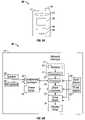
- FIG. 2is a system block diagram illustrating one embodiment of an electronic device that may incorporate aspects of the invention.
- the electronic deviceincludes a processor 21 which may be any general purpose single- or multi-chip microprocessor such as an ARM, Pentium®, Pentium II®, Pentium III®, Pentium IV®, Pentium® Pro, an 8051, a MIPS®, a Power PC®, an ALPHA®, or any special purpose microprocessor such as a digital signal processor, microcontroller, or a programmable gate array.
- the processor 21may be configured to execute one or more software modules.
- the processormay be configured to execute one or more software applications, including a web browser, a telephone application, an email program, or any other software application.
- the processor 21is also configured to communicate with an array driver 22 .
- the array driver 22includes a row driver circuit 24 and a column driver circuit 26 that provide signals to a display array or panel 30 .
- the cross section of the array illustrated in FIG. 1is shown by the lines 1 - 1 in FIG. 2 .
- the row/column actuation protocolmay take advantage of a hysteresis property of these devices illustrated in FIG. 3 . It may require, for example, a 10 volt potential difference to cause a movable layer to deform from the relaxed state to the actuated state. However, when the voltage is reduced from that value, the movable layer maintains its state as the voltage drops back below 10 volts.
- the movable layerdoes not relax completely until the voltage drops below 2 volts.
- a window of applied voltageabout 3 to 7 V in the example illustrated in FIG. 3 , within which the device is stable in either the relaxed or actuated state. This is referred to herein as the “hysteresis window” or “stability window.”
- the row/column actuation protocolcan be designed such that during row strobing, pixels in the strobed row that are to be actuated are exposed to a voltage difference of about 10 volts, and pixels that are to be relaxed are exposed to a voltage difference of close to zero volts.
- each pixelsees a potential difference within the “stability window” of 3-7 volts in this example.
- This featuremakes the pixel design illustrated in FIG. 1 stable under the same applied voltage conditions in either an actuated or relaxed pre-existing state. Since each pixel of the interferometric modulator, whether in the actuated or relaxed state, is essentially a capacitor formed by the fixed and moving reflective layers, this stable state can be held at a voltage within the hysteresis window with almost no power dissipation. Essentially no current flows into the pixel if the applied potential is fixed.
- a display framemay be created by asserting the set of column electrodes in accordance with the desired set of actuated pixels in the first row.
- a row pulseis then applied to the row 1 electrode, actuating the pixels corresponding to the asserted column lines.
- the asserted set of column electrodesis then changed to correspond to the desired set of actuated pixels in the second row.
- a pulseis then applied to the row 2 electrode, actuating the appropriate pixels in row 2 in accordance with the asserted column electrodes.
- the row 1 pixelsare unaffected by the row 2 pulse, and remain in the state they were set to during the row 1 pulse. This may be repeated for the entire series of rows in a sequential fashion to produce the frame.
- the framesare refreshed and/or updated with new display data by continually repeating this process at some desired number of frames per second.
- protocols for driving row and column electrodes of pixel arrays to produce display framesare also well known and may be used in conjunction with the present invention.
- FIGS. 4 , 5 A, and 5 Billustrate one possible actuation protocol for creating a display frame on the 3 ⁇ 3 array of FIG. 2 .
- FIG. 4illustrates a possible set of column and row voltage levels that may be used for pixels exhibiting the hysteresis curves of FIG. 3 .
- actuating a pixelinvolves setting the appropriate volts, respectively Relaxing the pixel is accomplished by setting the appropriate column to +V bias , and the appropriate row to the same + ⁇ V, producing a zero volt potential difference across the pixel. In those rows where the row voltage is held at zero volts, the pixels are stable in whatever state they were originally in, regardless of whether the column is at +V bias , or ⁇ V bias .
- actuating a pixelcan involve setting the appropriate column to +V bias , and the appropriate row to ⁇ V.
- releasing the pixelis accomplished by setting the appropriate column to ⁇ V bias , and the appropriate row to the same ⁇ V , producing a zero volt potential difference across the pixel.
- FIG. 5Bis a timing diagram showing a series of row and column signals applied to the 3 ⁇ 3 array of FIG. 2 which will result in the display arrangement illustrated in FIG. 5A , where actuated pixels are non-reflective.
- the pixelsPrior to writing the frame illustrated in FIG. 5A , the pixels can be in any state, and in this example, all the rows are at 0 volts, and all the columns are at +5 volts. With these applied voltages, all pixels are stable in their existing actuated or relaxed states.
- pixels ( 1 , 1 ), ( 1 , 2 ), ( 2 , 2 ), ( 3 , 2 ) and ( 3 , 3 )are actuated.
- columns 1 and 2are set to ⁇ 5 volts
- column 3is set to +5 volts. This does not change the state of any pixels, because all the pixels remain in the 3-7 volt stability window.
- Row 1is then strobed with a pulse that goes from 0, up to 5 volts, and back to zero. This actuates the ( 1 , 1 ) and ( 1 , 2 ) pixels and relaxes the ( 1 , 3 ) pixel. No other pixels in the array are affected.
- row 2is set to ⁇ 5 volts, and columns 1 and 3 are set to +5 volts.
- the same strobe applied to row 2will then actuate pixel ( 2 , 2 ) and relax pixels ( 2 , 1 ) and ( 2 , 3 ). Again, no other pixels of the array are affected.
- Row 3is similarly set by setting columns 2 and 3 to ⁇ 5 volts, and column 1 to +5 volts.
- the row 3strobe sets the row 3 pixels as shown in FIG. 5A . After writing the frame, the row potentials are zero, and the column potentials can remain at either +5 or ⁇ 5 volts, and the display is then stable in the arrangement of FIG. 5A .
- FIGS. 6A and 6Bare system block diagrams illustrating an embodiment of a display device 40 .
- the display device 40can be, for example, a cellular or mobile telephone.
- the same components of display device 40 or slight variations thereofare also illustrative of various types of display devices such as televisions and portable media players.
- the display device 40includes a housing 41 , a display 30 , an antenna 43 , a speaker 45 , an input device 48 , and a microphone 46 .
- the housing 41is generally formed from any of a variety of manufacturing processes as are well known to those of skill in the art, including injection molding and vacuum forming.
- the housing 41may be made from any of a variety of materials, including, but not limited to, plastic, metal, glass, rubber, and ceramic, or a combination thereof.
- the housing 41includes removable portions (not shown) that may be interchanged with other removable portions of different color, or containing different logos, pictures, or symbols.
- the display 30 of exemplary display device 40may be any of a variety of displays, including a bi-stable display, as described herein.
- the display 30includes a flat-panel display, such as plasma, EL, OLED, STN LCD, or TFT LCD as described above, or a non-flat-panel display, such as a CRT or other tube device, as is well known to those of skill in the art.
- the display 30includes an interferometric modulator display, as described herein.
- the components of one embodiment of exemplary display device 40are schematically illustrated in FIG. 6B .
- the illustrated exemplary display device 40includes a housing 41 and can include additional components at least partially enclosed therein.
- the exemplary display device 40includes a network interface 27 that includes an antenna 43 , which is coupled to a transceiver 47 .
- the transceiver 47is connected to a processor 21 , which is connected to conditioning hardware 52 .
- the conditioning hardware 52may be configured to condition a signal (e.g., filter a signal).
- the conditioning hardware 52is connected to a speaker 45 and a microphone 46 .
- the processor 21is also connected to an input device 48 and a driver controller 29 .
- the driver controller 29is coupled to a frame buffer 28 and to an array driver 22 , which in turn is coupled to a display array 30 .
- a power supply 50provides power to all components as required by the particular exemplary display device 40 design.
- the network interface 27includes the antenna 43 and the transceiver 47 so that the exemplary display device 40 can communicate with one or more devices over a network. In one embodiment, the network interface 27 may also have some processing capabilities to relieve requirements of the processor 21 .
- the antenna 43is any antenna known to those of skill in the art for transmitting and receiving signals. In one embodiment, the antenna transmits and receives RF signals according to the IEEE 802.11 standard, including IEEE 802.11(a), (b), or (g). In another embodiment, the antenna transmits and receives RF signals according to the BLUETOOTH standard. In the case of a cellular telephone, the antenna is designed to receive CDMA, GSM, AMPS, or other known signals that are used to communicate within a wireless cell phone network.
- the transceiver 47pre-processes the signals received from the antenna 43 so that they may be received by and further manipulated by the processor 21 .
- the transceiver 47also processes signals received from the processor 21 so that they may be transmitted from the exemplary display device 40 via the antenna 43 .
- the transceiver 47can be replaced by a receiver.
- the network interface 27can be replaced by an image source, which can store or generate image data to be sent to the processor 21 .
- the image sourcecan be a digital video disc (DVD) or a hard-disc drive that contains image data, or a software module that generates image data.
- the processor 21generally controls the overall operation of the exemplary display device 40 .
- the processor 21receives data, such as compressed image data from the network interface 27 or an image source, and processes the data into raw image data or into a format that is readily processed into raw image data.
- the processor 21then sends the processed data to the driver controller 29 or to frame buffer 28 for storage.
- Raw datatypically refers to the information that identifies the image characteristics at each location within an image. For example, such image characteristics can include color, saturation, and gray-scale level.
- the processor 21includes a microcontroller, CPU, or logic unit to control operation of the exemplary display device 40 .
- Conditioning hardware 52generally includes amplifiers and filters for transmitting signals to the speaker 45 , and for receiving signals from the microphone 46 .
- Conditioning hardware 52may be discrete components within the exemplary display device 40 , or may be incorporated within the processor 21 or other components.
- the driver controller 29takes the raw image data generated by the processor 21 either directly from the processor 21 or from the frame buffer 28 and reformats the raw image data appropriately for high speed transmission to the array driver 22 . Specifically, the driver controller 29 reformats the raw image data into a data flow having a raster-like format, such that it has a time order suitable for scanning across the display array 30 . Then the driver controller 29 sends the formatted information to the array driver 22 .
- a driver controller 29such as a LCD controller, is often associated with the system processor 21 as a stand-alone Integrated Circuit (IC), such controllers may be implemented in many ways. They may be embedded in the processor 21 as hardware, embedded in the processor 21 as software, or fully integrated in hardware with the array driver 22 .
- the array driver 22receives the formatted information from the driver controller 29 and reformats the video data into a parallel set of waveforms that are applied many times per second to the hundreds and sometimes thousands of leads coming from the display's x-y matrix of pixels.
- the driver controller 29 , array driver 22 , and display array 30are appropriate for any of the types of displays described herein.
- the driver controller 29is a conventional display controller or a bi-stable display controller (e.g., an interferometric modulator controller).
- the array driver 22is a conventional driver or a bi-stable display driver (e.g., an interferometric modulator display).
- a driver controller 29is integrated with the array driver 22 .
- display array 30is a typical display array or a bi-stable display array (e.g., a display including an array of interferometric modulators).
- the input device 48allows a user to control the operation of the exemplary display device 40 .
- the input device 48includes a keypad, such as a QWERTY keyboard or a telephone keypad, a button, a switch, a touch-sensitive screen, or a pressure- or heat-sensitive membrane.
- the microphone 46is an input device for the exemplary display device 40 . When the microphone 46 is used to input data to the device, voice commands may be provided by a user for controlling operations of the exemplary display device 40 .
- the power supply 50can include a variety of energy storage devices as are well known in the art.
- the power supply 50is a rechargeable battery, such as a nickel-cadmium battery or a lithium ion battery.
- the power supply 50is a renewable energy source, a capacitor, or a solar cell including a plastic solar cell, and solar-cell paint.
- the power supply 50is configured to receive power from a wall outlet.
- control programmabilityresides, as described above, in a driver controller which can be located in several places in the electronic display system. In some embodiments, control programmability resides in the array driver 22 . Those of skill in the art will recognize that the above-described optimizations may be implemented in any number of hardware and/or software components and in various configurations.
- FIGS. 7A-7Eillustrate five different embodiments of the movable reflective layer 14 and its supporting structures.
- FIG. 7Ais a cross section of the embodiment of FIG. 1 , where a strip of metal material 14 is deposited on orthogonally extending supports 18 .
- FIG. 7Bthe moveable reflective layer 14 is attached to supports at the corners only, on tethers 32 .
- FIG. 7Cthe moveable reflective layer 14 is suspended from a deformable layer 34 , which may comprise a flexible metal.
- the deformable layer 34connects, directly or indirectly, to the substrate 20 around the perimeter of the deformable layer 34 .
- connectionscan take the form of continuous walls and/or individual posts.
- parallel railscan support crossing rows of deformable layer 34 materials, thus defining columns of pixels in trenches and/or cavities between the rails. Additional support posts within each cavity can serve to stiffen the deformable layer 34 and prevent sagging in the relaxed position.
- the embodiment illustrated in FIG. 7Dhas support post plugs 42 upon which the deformable layer 34 rests.
- the movable reflective layer 14remains suspended over the gap, as in FIGS. 7A-7C , but the deformable layer 34 does not form the support posts by filling holes between the deformable layer 34 and the optical stack 16 . Rather, the support posts are formed of a planarization material, which is used to form support post plugs 42 .
- the embodiment illustrated in FIG. 7Eis based on the embodiment shown in FIG. 7D , but may also be adapted to work with any of the embodiments illustrated in FIGS. 7A-7C , as well as additional embodiments not shown. In the embodiment shown in FIG. 7E , an extra layer of metal or other conductive material has been used to form a bus structure 44 . This allows signal routing along the back of the interferometric modulators, eliminating a number of electrodes that may otherwise have had to be formed on the substrate 20 .
- the interferometric modulatorsfunction as direct-view devices, in which images are viewed from the front side of the transparent substrate 20 , the side opposite to that upon which the modulator is arranged.
- the reflective layer 14optically shields the portions of the interferometric modulator on the side of the reflective layer opposite the substrate 20 , including the deformable layer 34 . This allows the shielded areas to be configured and operated upon without negatively affecting the image quality.
- Such shieldingallows the bus structure 44 in FIG. 7E , which provides the ability to separate the optical properties of the modulator from the electromechanical properties of the modulator, such as addressing and the movements that result from that addressing.
- This separable modulator architectureallows the structural design and materials used for the electromechanical aspects and the optical aspects of the modulator to be selected and to function independently of each other.
- the embodiments shown in FIGS. 7C-7Ehave additional benefits deriving from the decoupling of the optical properties of the reflective layer 14 from its mechanical properties, which are carried out by the deformable layer 34 .
- Thisallows the structural design and materials used for the reflective layer 14 to be optimized with respect to the optical properties, and the structural design and materials used for the deformable layer 34 to be optimized with respect to desired mechanical properties.
- some embodiments of the disclosed interferometric modulatorare fabricated using methods in which portions or all of one or more sacrificial materials are substantially etched away in one or more steps of a manufacturing process, for example, as disclosed in U.S. Patent Publication No. 2004/0051929 A1. Such an etching process is also referred to herein as a “release etch.”
- a device comprising a sacrificial materialis contacted with an etchant that selectively etches away the sacrificial material.
- the etchantis a vapor phase etchant, for example, XeF 2 , and substantially all of the etching products are also in the vapor phase.
- the sacrificial materialis selectively etched over other, non-sacrificial materials that contact the etchant.
- a material for which etching is desired in a particular etching stepis also referred to herein as a “target material.”
- a material for which etching is not desired in a particular etching stepis also referred to herein as a “structural material,” although those skilled in the art will understand that a structural material does not necessarily have a structural function in the final device.
- a structural material in one stepcan be a target material in another step.
- a sacrificial materialis a structural material in one or more steps and a target material in another step. Accordingly, those skilled in the art will understand that the etching conditions in a particular step will determine whether a material is a target material or a structural material.
- FIGS. 8A-8Eillustrate in cross section devices 800 used in some embodiments of a method for fabricating the devices illustrated in FIGS. 7A-7E .
- Each of these devices 800comprises a sacrificial material 860 disposed in a volume that is a cavity in the corresponding devices illustrated in FIGS. 7A-7E .
- the devices illustrated in FIGS. 8A-8Eare also referred to herein as “unreleased,” and the devices illustrated in FIGS.
- a process from etching away the sacrificial material 860is referred to herein as a “release etch.”
- These devicealso comprise one or more etch holes (not illustrated) formed, for example, in the deformable layer 34 through which an etchant accesses the sacrificial material 860 in a release etch process.
- the etchantalso accesses the sacrificial material 860 from open sides of the interferometric modulator arrays.
- contacting the devices 800 illustrated in any of FIGS. 8A-8E to a vapor phase etchant, for example, XeF 2provides the devices illustrated in FIGS.
- the sacrificial material 860comprise one or more layers.
- the sacrificial material 860comprises a material etchable by XeF 2 , for example, silicon, titanium, zirconium, hafnium, vanadium, tantalum, niobium, molybdenum, tungsten, and combinations thereof.
- the optical stack 816 in some embodiments of the disclosed interferometric modulatorscomprise a dielectric layer 816 a formed over a partially reflective layer 816 b and a conductive layer 816 c , for example, as illustrated in FIG. 8C .
- the dielectric layer 816 acomprises silicon dioxide.
- etching away a molybdenum sacrificial layer 860 with a thickness of from about 0.15 ⁇ m to about 0.7 ⁇ m using XeF 2the silicon dioxide dielectric layer 816 a was also etched to a depth of up to about 500 ⁇ , which is significant in a dielectric layer with an original thickness of about 1000 ⁇ . In other words, the etching is not as selective as desired for preferentially etching molybdenum over silicon dioxide.
- sacrificial materialsare often disposed under and/or between one or more non-sacrificial materials with structural, electrical, and/or optical functions.
- Undesired etching of the structural and/or optical componentscan result in failure of the device and/or changes in the physical and/or optical properties of the device, for example, changes in the color of a pixel.
- undesired etchingis particularly acute at or around openings in a device that provide etchant access to the sacrificial material.
- the observed etching selectivity between a target material and a structural material in a confined volumeis different from the selectivity of the same materials in an unconfined configuration.
- the confined volumeresults in extended contact between the target and structural materials with, for example, excess etchant, etching byproducts, and/or etching intermediates.
- excess etchantetching byproducts
- etching intermediatesare effective etchants for the target material and/or the structural material. Because the etching selectivities of these compounds are different from the etching selectivity of the etchant, the observed or effective etching selectivity depends on the relative concentrations of all of the active etching species.
- an etching process in a confined volumeexhibits a lower effective selectivity than would be otherwise expected based on known and/or measured etching rates of the respective bulk materials.
- FIG. 9Aillustrates a cross section of an unreleased interferometric modulator array 900 comprising a red interferometric modulator 900 a , a green interferometric modulator 900 b , and a blue interferometric modulator 900 c similar to the unreleased interferometric modulator illustrated in FIG. 8A .
- FIGS. 9A-9Dillustrate supports 918 corresponding to each of the interferometric modulators 900 a , 900 b , and 900 c .
- the red interferometric modulator 900 acomprises supports 918 a
- the green interferometric modulator 900 bcomprises supports 918 b
- the blue interferometric modulator 900 ccomprises supports 918 c .
- supports 918 care longer than supports 918 b , which are in turn, longer than supports 918 a .
- Deformable layers 914 a , 914 b , and 914 c corresponding to interferometric modulators 900 a , 900 b , and 900 care formed over the supports 918 a , 918 b , and 918 c , respectively.
- a layer of sacrificial material 960 a , 960 b , and 960 cDisposed between the optical stack 916 and each of the deformable layers 914 a , 914 b , and 914 c is a layer of sacrificial material 960 a , 960 b , and 960 c .
- the array 900is not drawn to scale.
- the thickness of the layers of sacrificial material 960 a , 960 b , and 960 care on the order of tenths of microns, while the overall widths of the interferometric modulators 900 a , 900 b , and 900 c are on the order of tens of microns. Accordingly, certain features in FIGS. 9A-9D are exaggerated for clarity.
- FIG. 9Billustrates the initial etching of the sacrificial layers 960 a , 960 b , and 960 c through the etch holes 970 , forming cavities 980 .
- the etchantaccesses the sacrificial layers 960 exclusively through the etching holes 970 .
- some embodiments of unreleased interferometric modulatorspermit etchant access through, for example, one or more of the sides of the device.
- the cavity 980extends to the optical stack 916 exposing a portion 916 c to the etchant, etching byproducts, and etching intermediates.
- the thinner sacrificial layer 960 c of blue interferometric modulator 900 cwill be completely etched away before sacrificial layers 960 b (green) and 960 a (red), as illustrated in FIG. 9C .
- the portion 916 c of the optical stack of the blue interferometric modulator 900 cis completely exposed to the etchant, while portions of the optical stack 916 b and 916 a of the green 900 b and red 900 a interferometric modulators are partially exposed.
- etching holes 970are formed in the deformable layers 914 a , 914 b , and 914 c .
- etchantaccesses the sacrificial layers 916 a , 916 b , and 916 c through an etching hole 970 , forming a cavity 980 generally centered on the etching hole 970 .
- the etch holes 970limit diffusion of fresh etchant into, and etching byproducts and intermediates out of the cavity 980 .
- Portions of the dielectric layer 916 exposed by the cavity 980experience increased etching by the etchant and/or etching by-products compared with unexposed portions, thereby forming dips 917 a , as best seen for the optical stack portion 916 c.
- the etchingis complete when the sacrificial layers 960 b and 960 a of the green and red interferometric modulator 900 b and 900 a are etched away, thereby completely exposing the portions of the optical stack 916 b and 916 a to the etchant, as illustrated in FIG. 9D .
- the optical stack 916 cis further etched relative to the state illustrated in FIG. 9C .
- etching selectivityis expressed as a ratio between an etching rate of a target material and an etching rate of a structural material.
- the etching rate for a particular materialwill differ depending on factors known in the art, for example, the identity of the etchant, etchant concentration, temperature, and the like.
- mass transportwhich affects, for example, the rate at which fresh etchant diffuses to the etching front, as well as the rate at which etching by-products diffuse away.
- etchantaccesses the sacrificial material 860 of the unreleased interferometric modulators illustrated in FIGS. 8A-8E through etch holes and from the sides of device.
- mass transport of the etchant, etching byproducts, and etching intermediates in such devicesdepends in part on the mean free path, which depends on factors known in the art, for example, on the size of the etching hole(s), the dimensions of the cavity, the shape of the cavity, and the like.
- the mean free pathchanges as the etching proceeds, for example, to regions remote from the etch holes and/or edges of the device.
- the etching rate of a target material and/or a structural material in a constrained volumeis different from the etching rate of the same material in an unconstrained volume, for example, on an outer surface of a device or in a bulk sample of the material.
- etching in the constrained volumeis slower, for example, when the etching reaction is limited by diffusion of fresh etchant to the etching front.
- etching in the constrained volumeis faster, for example, when etching byproducts and/or intermediates trapped within the cavity are active etchants.
- the observed etching rate of a target or structural materialdepends at least in part on the shape, size, and dimensions of the constrained volume. Because these factors change over the course of an etching reaction, one or more of the etching rates also changes in some embodiments. Such considerations make the a priori determination of an etching rate of a target or structural material under such conditions difficult. Accordingly, in many cases, the etching rates of target and/or structural are determined empirically, for example, on a device-by-device basis.
- etching ratesare expressed as average etching rates over an entire etching process. In other embodiments, etching rates are expressed as average etching rates over a portion of an etching process. In other embodiments, etching rates are expressed as rates at one or more particular time points in an etching process. Unless otherwise specified, etching rates disclosed herein are average rates over an entire etching process. Etching rates are also expressible in units of mass per time (e.g., g/sec), amount per time (e.g., mol/sec), volume per time (e.g., mL/sec), and/or distance per time (e.g., ⁇ m/sec). Etching rates are typically expressed in distance per time herein, although those skilled in the art will understand that the rates are equivalently expressible using different units.
- etching selectivity in the illustrated embodimentis expressible as a ratio between an etching rate of the sacrificial material 960 and an etching rate of the dielectric layer of the optical stack 916 within the cavity 980 .
- at least one of the target material or structural materialis not in a constrained volume.
- a target materialis disposed in a constrained volume in a device and a structural material of interest is disposed on an exterior of the device, and the relevant relative rate between is between the materials in these environments.
- an etching selectivity between the target material and the structural material in the absence of a co-etchantis at least 20:1, preferably, at least 50:1, more preferably, at least 100:1, most preferably, at least 200:1. In some preferred embodiments, the etching selectivity is at least 300:1, at least 400:1, or at least 500:1.
- Embodiments of the methodinclude a quantity of a co-etchant effective to improve the selectivity by at least about 2-times, preferably, at least about 4 -times, more preferably, at least about 5-times, most preferably, at least about 10-times compared with a similar etching reaction not using a co-etchant. In some embodiments, the improvement in selectivity is at least about 20-times, at least about 50-times, or at least about 100-times.
- interferometric modulator fabricationinclude a release etch step for a molybdenum layer with about a 20 ⁇ m undercut, for example, as illustrated in FIGS. 9A-9D .
- an underlying SiO 2 layeris etched about 500 ⁇ during the etching of the molybdenum. Accordingly, the selectivity of this particular etching reaction is about 400:1 (20 ⁇ m/500 ⁇ ).
- the SiO 2 layeris etched by not more than about 50 ⁇ , which translates into an etching selectivity of at least 4000:1, or at least about a 10-time improvement in selectivity.
- the selectivity of an etching processis different for materials in an unconstrained volume, for example, for the bulk materials.
- the etching rate of bulk SiO 2is about 1 ⁇ /min and of bulk molybdenum is about 3 ⁇ m/min (about 1-5 ⁇ m/min), for an etching selectivity of about 30,000:1.
- FIG. 10illustrates an embodiment of an optical stack 1016 formed on a glass substrate 1020 .
- a sacrificial layer 1060is formed over the optical stack 1016 .
- the optical stack 1016comprises an etch stop 1016 b formed over the dielectric layer 1016 a .
- the etch stop 1016 bcomprises a material which is more resistant to etching in the release etch than the dielectric layer 1016 a .
- the etch stop 1016 bcomprises aluminum oxide (Al 2 O 3 ), which is highly resistant to etching in some embodiments of release etch processes, thereby preventing etching of the dielectric layer 1016 a .
- Some embodiments of an aluminum oxide etch stop 1016 bexhibit one or more of the following disadvantages, however: additional steps for forming the etch stop layer 1016 b , charge trapping in the etch stop layer 1016 b , and high surface energy.
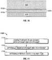
- FIG. 11is a flowchart illustrating an embodiment of an etching method 1100 exhibiting improved selectivity between a target material and a structural material, for example, molybdenum and silicon dioxide, thereby eliminating the need for an etch stop layer to protect the structural material.
- a device-to-be-etchedis contemporaneously contacted with an etchant and a co-etchant.
- the etchant and co-etchantare optionally removed, for example, by purging with a gas and/or under vacuum.
- steps 1110 and 1120are optionally repeated.
- some embodimentsuse an etching apparatus with an insufficient volume to hold enough vapor phase etchant to completely etch a device in a single cycle. Some embodiments use different ratios of the vapor phase etchant and co-etchant in different cycles. In some embodiments, purging between etching cycles removes reactive etching byproducts and/or intermediates, thereby improving selectivity. Embodiments of the method are useful for the fabrication of MEMS devices comprising hole or cavities, for example, for the release etch of any of the unreleased interferometric modulators illustrated in FIGS. 8A-8E to form the corresponding released interferometric modulators illustrated in FIGS. 7A-7E .
- the etchantis a vapor phase etchant, for example, one or more gaseous halides known in the art.
- suitable gaseous halidesinclude noble gas fluorides, interhalogen fluorides, interhalogen chlorides, NF 3 , combinations thereof, and the like.
- the etchantis XeF 2 , which is a noble gas fluoride.
- the pressure of the etchant over at least a portion of the etching processis from about 0.5 torr to about 500 torr, more preferably, from about 1 torr to about 50 torr, most preferably, from about 2 torr to about 10 torr.
- the pressureis a partial pressure. As the etching proceeds, the partial pressure of the etchant declines. Those skilled in the art will understand that different pressures are suitable for different etchants.
- the co-etchantcomprises one or more oxygen-containing compounds, one or more sulfur-containing compounds, one or more nitrogen-containing compounds, or combinations thereof.
- Suitable oxygen-containing compoundsinclude O 2 , O 3 , ozonides, peroxides, peracids, superoxides, nitrogen oxides (N x O y ), sulfur oxides (S x O y ), and combinations thereof.
- Suitable sulfur-containing compoundsinclude thiols, sulfides, thiones, thioic acids, carbon disulfide, OCS, and combinations thereof.
- Suitable nitrogen-containing compoundsinclude amines, amides, azides, and combinations thereof.
- the co-etchantis a vapor phase co-etchant.
- the pressure of the co-etchant over at least a portion of the etching processis from about 0.5 torr to about 500 torr, more preferably, from about 1 torr to about 50 torr, most preferably, from about 2 torr to about 10 torr.
- the etching processis performed at from about 0° C. to about 200° C., preferably, from about 10° C. to about 100° C., most preferably from about 20° C. to about 50° C.
- the overall pressure over at least a portion of the etching processis from about 0.5 torr to about 1000 torr, preferably, from about 1 torr to about 500 torr, most preferably, from about 5 torr to about 100 torr.
- vapor phaserefers to compounds for which an effective amount of the compound is in the vapor phase under the etching conditions. As such, in some embodiments, at least some of the compound is not in the vapor phase, that is, is in a condensed phase, for example, solid and/or liquid phases.
- Methods for generating a vapor phase concentration of a compoundare known in the art, for example, heating, sparging, atomizing, irradiating, combinations thereof, and the like.
- Suitable target materialsinclude group IVA ( 14 ) semiconductors, III-V (13-15) semiconductors, metals, transition metals, and combinations, mixtures, solutions, and alloys thereof.
- Suitable target materialsinclude silicon, titanium, zirconium, hafnium, vanadium, tantalum, niobium, molybdenum, tungsten, and combinations thereof.
- the target materialcomprises a metal, for example, titanium, zirconium, hafnium, vanadium, tantalum, niobium, molybdenum, tungsten, and combinations thereof.
- the target materialcomprises molybdenum.
- Suitable structural materialsinclude metal oxides, nitrides, sulfides, combinations thereof, and the like. Other suitable structural materials include metals, metal alloys, photoresist materials, organic materials, combinations thereof, and the like.
- Some embodimentsfurther comprise activation of the etching process, by means known in the art, for example, using thermal, ultrasonic, microwave, ultraviolet (UV), laser, or combination energy.
- activation of the etching processby means known in the art, for example, using thermal, ultrasonic, microwave, ultraviolet (UV), laser, or combination energy.
- a series of test devices 1200 illustrated in FIG. 12Awere manufactured, each of with comprised a dielectric layer 1210 , a molybdenum layer 1220 formed over the dielectric layer 1210 , and a photoresist layer 1230 partially covering the molybdenum layer 1220 , thereby forming an exposed region 1222 .
- the dielectric layer 1210was either sputtered silicon dioxide (450 ⁇ 50 ⁇ ) or alumina-magnesium oxide-calcium oxide-soda glass.
- Two different types of molybdenum layers 1220referred to as low-density and high-density, respectively, were formed on the substrate 1210 by sputtering (physical vapor deposition, PVD).
- the low-density layerhad a density of less than about 5 g/cm 3 and a thickness of about 2000 ⁇ .
- the high-density layerhad a density of greater than about 5 g/cm 3 and a thickness of about 1700 ⁇ .
- the photoresist layer 1230was an I-line photoresist spin-coated and patterned, with a thickness of about 2 ⁇ m. These devices 1200 simulate the etching of a target material to form a cavity bounded by structural materials in the manufacture of a MEMS device, for example, in a release etch of an unreleased interferometric modulator as illustrated in FIG. 9A .
- the exposed region 1222corresponds, for example, to a partially opened cavity, the photoresist layer 1230 to the deformable layer, the dielectric layer 1210 to the dielectric layer of an optical stack, and the molybdenum layer 1220 to a sacrificial material.
- the apparatus 1300comprises an etching chamber 1310 , fluidly connected with an expansion chamber 1320 though a valve 1322 .
- the expansion chamber 1320is fluidly connected with a XeF 2 vessel 1330 through a valve 1332 .
- a vacuum source 1340is fluidly connected with the etching chamber 1310 through a valve 1342 .
- a substrate support 1312is disposed in the etching chamber 1310 .
- the expansion chamber 1320is equipped with a gas inlet, which is controlled by a valve 1324 , used, for example, for introducing a vapor phase co-etchant.
- the vacuum source 1340 and the expansion chamber 1320are fluidly connected through a valve 1344 .
- Etching of the test deviceswas performed as follows. Solid XeF 2 was loaded in the XeF 2 vessel 1330 . A test device was loaded onto the substrate support 1312 .
- One etching cyclecomprised the following steps. Valves 1332 and 1344 were opened and the etching chamber 1310 and expansion chamber 1320 evacuated. Valves 1342 and 1344 were closed, then valve 1332 opened to permit XeF 2 vapor to fill the expansion chamber 1320 . At 25° C., the vapor pressure of XeF 2 is about 3.8 Torr (0.5 kPa). Valve 1332 was then closed and O 2 mixed with the XeF 2 vapor in the expansion chamber though gas inlet valve 1324 .
- Valve 1322was then opened for a charging time, then closed, thereby filling the etching chamber with and exposing the device to the etchant (XeF 2 ) and co-etchant (O 2 ). After the device was etched for an etching time, valve 1342 was opened to remove the etchant and co-etchant from the etching chamber 1310 .
- the total pressure of the XeF 2 +O 2was from about 4 torr to about 50 torr.
- the etchingwas performed at room temperature or at about 50° C. with one or two etching cycles, each with a 120 sec charge time and a 300 sec etch time. As illustrated in FIG. 12B , etching the molybdenum layer 1220 forms an undercut 1222 below the photoresist layer 1230 .
- the width of the undercut 1222was determined by optical microscopy.
- the photoresist 1230was then stripped using acetone with an isopropanol rinse to provide the structure illustrated in FIG. 12C comprising a molybdenum layer 1220 overlying part of the dielectric layer 1210 .
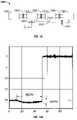
- the presence and dimensions of a dip 1212 in the dielectric layer 1210was determined using a Tencor P20 profilometer (KLA-Tencor, San Jose, Calif.). It is believed that the dip 1212 is localized in the undercut area 1222 because the relatively poorer mass transport in this region increases the concentration of reactive etching intermediates and/or by-products, which as discussed below, are believed to contribute to the etching of the structural material. Results are summarized in TABLE 1 , where the proportion of O 2 :XeF 2 is on a molar basis, in these experiments, the ratio of their pressures. Each value is the average of three test runs.
- FIGS. 14A and 14BProfilometry results for experiments 1 and 6 are illustrated in FIGS. 14A and 14B , respectively.
- the co-etchantimproved the selectivity of the etching in both types of test devices, and increasing the amount of co-etchant increased the selectivity.
- adding the co-etchantdid not significantly change the etch rate compared with the etch rate without a co-etchant.
- XPSX-ray photoelectron spectroscopy
- SIMSsecondary ion mass spectroscopy
- the target materialis molybdenum
- the structural materialis silicon dioxide
- the etchantis XeF 2
- the co-etchantis O 2 .
- silicon dioxideis etched by some combination of two mechanisms: direct etching by XeF 2 and/or etching by reactive molybdenum fluoride species.
- the reaction of silicon dioxide with XeF 2is thermodynamically favorable, but kinetically unfavorable (Eq. 2).
- SiO 2 (s)+2XeF 2 (g) ⁇ SiF 4 (g)+2Xe (g)+O 2 ( g) ⁇ H°⁇ 358 kJ/mol Eq.
- O 2reacts with other reactive species present, for example, XeF ⁇ , F ⁇ , MoO x , and/or SiF y to produce less reactive products. Furthermore, because one of the products in the reaction of XeF 2 with SiO 2 (Eq. 2) is O 2 , it is believed that adding O 2 inhibits this reaction by mass action.
Landscapes
- Physics & Mathematics (AREA)
- Engineering & Computer Science (AREA)
- Spectroscopy & Molecular Physics (AREA)
- General Physics & Mathematics (AREA)
- Optics & Photonics (AREA)
- Geometry (AREA)
- Manufacturing & Machinery (AREA)
- Microelectronics & Electronic Packaging (AREA)
- Mechanical Light Control Or Optical Switches (AREA)
- Micromachines (AREA)
- Drying Of Semiconductors (AREA)
Abstract
Description
| TABLE I | |||||
| Dip | Dip | ||||
| Undercut | width | depth | |||
| Entry | Mo/dielectric | O2:XeF2 | (μm) | (μm) | (Å) |
| 1 | Low density/ | 0 | 40 | 47 | 170 |
| 2 | Low density/ | 1 | 35 | 40 | 110 |
| 3 | Low density/ | 10 | 35 | 41 | 90 |
| 4 | High density/ | 0 | 15 | 18 | 110 |
| 5 | High density/ | 1 | 18 | no dip | no dip |
| 6 | High density/ | 10 | 12 | no dip | no dip |
Mo (s)+3XeF2(g)→MoF6(g)+3Xe (g) Eq. 1
This reaction also forms lower molybdenum fluorides (MoFx, x=1-5) as byproducts.
SiO2(s)+2XeF2(g)→SiF4(g)+2Xe (g)+O2( g) ΔH°=−358 kJ/mol Eq. 2
Also formed in the etching process are unstable intermediates generated from XeF2, for example, XeF− and F−, as well as lower silicon fluorides (SiFy, y=1-3). It is believed that these species, as well as the lower molybdenum fluoride species discussed above can react with or activate SiO2. The reaction of MoF6with SiO2to form SiF4is also thermodynamically favorable (Eq. 3).
SiO2(s)+2MoF6(g)→SiF4(g)+2MoOF4(g)ΔH°=−99 kJ/mol Eq. 3
It is believed that MoOF4does not react with SiO2under the etching conditions because the reaction is thermodynamically unfavorable (Eq. 4).
SiO2(s)+2MoOF4(g)→SiF4(g)+2MoO2F2(g)ΔH°=+378 kJ/mol Eq. 4
2Mo (s)+4XeF2(g)+O2(g)→2MoOF4(g)+4Xe (g) Eq. 5
Claims (37)
Priority Applications (3)
| Application Number | Priority Date | Filing Date | Title |
|---|---|---|---|
| US11/497,726US7566664B2 (en) | 2006-08-02 | 2006-08-02 | Selective etching of MEMS using gaseous halides and reactive co-etchants |
| PCT/US2007/016353WO2008100279A2 (en) | 2006-08-02 | 2007-07-18 | Selective etching of mems using gaseous halides and reactive co-etchants |
| TW096128431ATW200821259A (en) | 2006-08-02 | 2007-08-02 | Selective etching of MEMS using gaseous halides and reactive co-etchants |
Applications Claiming Priority (1)
| Application Number | Priority Date | Filing Date | Title |
|---|---|---|---|
| US11/497,726US7566664B2 (en) | 2006-08-02 | 2006-08-02 | Selective etching of MEMS using gaseous halides and reactive co-etchants |
Publications (2)
| Publication Number | Publication Date |
|---|---|
| US20080032439A1 US20080032439A1 (en) | 2008-02-07 |
| US7566664B2true US7566664B2 (en) | 2009-07-28 |
Family
ID=39029691
Family Applications (1)
| Application Number | Title | Priority Date | Filing Date |
|---|---|---|---|
| US11/497,726Expired - Fee RelatedUS7566664B2 (en) | 2006-08-02 | 2006-08-02 | Selective etching of MEMS using gaseous halides and reactive co-etchants |
Country Status (3)
| Country | Link |
|---|---|
| US (1) | US7566664B2 (en) |
| TW (1) | TW200821259A (en) |
| WO (1) | WO2008100279A2 (en) |
Cited By (44)
| Publication number | Priority date | Publication date | Assignee | Title |
|---|---|---|---|---|
| US20070268201A1 (en)* | 2006-05-22 | 2007-11-22 | Sampsell Jeffrey B | Back-to-back displays |
| US20080130089A1 (en)* | 1994-05-05 | 2008-06-05 | Idc, Llc | METHOD OF FABRICATING MEMS DEVICES (SUCH AS IMod) COMPRISING USING A GAS PHASE ETCHANT TO REMOVE A LAYER |
| US20080218834A1 (en)* | 2007-03-08 | 2008-09-11 | Qualcomm Mems Technologies, Inc. | Method and apparatus for providing a light absorbing mask in an interferometric modulator display |
| US20100079847A1 (en)* | 2008-09-30 | 2010-04-01 | Qualcomm Mems Technologies, Inc. | Multi-thickness layers for mems and mask-saving sequence for same |
| US20100085625A1 (en)* | 2007-07-02 | 2010-04-08 | Qualcomm Mems Technologies, Inc. | Electromechanical device with optical function separated from mechanical and electrical function |
| US7847999B2 (en) | 2007-09-14 | 2010-12-07 | Qualcomm Mems Technologies, Inc. | Interferometric modulator display devices |
| US20100328755A1 (en)* | 2006-06-15 | 2010-12-30 | Qualcomm Mems Technologies, Inc. | Apparatuses with enhanced low range bit depth |
| US7889417B2 (en) | 2007-05-09 | 2011-02-15 | Qualcomm Mems Technologies, Inc. | Electromechanical system having a dielectric movable membrane |
| US7898723B2 (en) | 2008-04-02 | 2011-03-01 | Qualcomm Mems Technologies, Inc. | Microelectromechanical systems display element with photovoltaic structure |
| US20110053379A1 (en)* | 2007-09-27 | 2011-03-03 | Lam Research Corporation | Profile control in dielectric etch |
| US7944604B2 (en) | 2008-03-07 | 2011-05-17 | Qualcomm Mems Technologies, Inc. | Interferometric modulator in transmission mode |
| US7969638B2 (en) | 2008-04-10 | 2011-06-28 | Qualcomm Mems Technologies, Inc. | Device having thin black mask and method of fabricating the same |
| US8023167B2 (en) | 2008-06-25 | 2011-09-20 | Qualcomm Mems Technologies, Inc. | Backlight displays |
| WO2011130718A2 (en) | 2010-04-16 | 2011-10-20 | Flex Lighting Ii, Llc | Front illumination device comprising a film-based lightguide |
| WO2011130715A2 (en) | 2010-04-16 | 2011-10-20 | Flex Lighting Ii, Llc | Illumination device comprising a film-based lightguide |
| US8054527B2 (en) | 2007-10-23 | 2011-11-08 | Qualcomm Mems Technologies, Inc. | Adjustably transmissive MEMS-based devices |
| US8058549B2 (en) | 2007-10-19 | 2011-11-15 | Qualcomm Mems Technologies, Inc. | Photovoltaic devices with integrated color interferometric film stacks |
| US8068269B2 (en) | 2008-03-27 | 2011-11-29 | Qualcomm Mems Technologies, Inc. | Microelectromechanical device with spacing layer |
| US8081373B2 (en) | 2007-07-31 | 2011-12-20 | Qualcomm Mems Technologies, Inc. | Devices and methods for enhancing color shift of interferometric modulators |
| US8115987B2 (en) | 2007-02-01 | 2012-02-14 | Qualcomm Mems Technologies, Inc. | Modulating the intensity of light from an interferometric reflector |
| US8164821B2 (en) | 2008-02-22 | 2012-04-24 | Qualcomm Mems Technologies, Inc. | Microelectromechanical device with thermal expansion balancing layer or stiffening layer |
| US8164815B2 (en) | 2007-03-21 | 2012-04-24 | Qualcomm Mems Technologies, Inc. | MEMS cavity-coating layers and methods |
| US8270056B2 (en) | 2009-03-23 | 2012-09-18 | Qualcomm Mems Technologies, Inc. | Display device with openings between sub-pixels and method of making same |
| US8270062B2 (en) | 2009-09-17 | 2012-09-18 | Qualcomm Mems Technologies, Inc. | Display device with at least one movable stop element |
| US8358266B2 (en) | 2008-09-02 | 2013-01-22 | Qualcomm Mems Technologies, Inc. | Light turning device with prismatic light turning features |
| US8488228B2 (en) | 2009-09-28 | 2013-07-16 | Qualcomm Mems Technologies, Inc. | Interferometric display with interferometric reflector |
| US8659816B2 (en) | 2011-04-25 | 2014-02-25 | Qualcomm Mems Technologies, Inc. | Mechanical layer and methods of making the same |
| US8736939B2 (en) | 2011-11-04 | 2014-05-27 | Qualcomm Mems Technologies, Inc. | Matching layer thin-films for an electromechanical systems reflective display device |
| US8797628B2 (en) | 2007-10-19 | 2014-08-05 | Qualcomm Memstechnologies, Inc. | Display with integrated photovoltaic device |
| US8797632B2 (en) | 2010-08-17 | 2014-08-05 | Qualcomm Mems Technologies, Inc. | Actuation and calibration of charge neutral electrode of a display device |
| US8817357B2 (en) | 2010-04-09 | 2014-08-26 | Qualcomm Mems Technologies, Inc. | Mechanical layer and methods of forming the same |
| US8830557B2 (en) | 2007-05-11 | 2014-09-09 | Qualcomm Mems Technologies, Inc. | Methods of fabricating MEMS with spacers between plates and devices formed by same |
| US8883026B2 (en) | 2012-03-29 | 2014-11-11 | SCREEN Holdings Co., Ltd. | Substrate processing method and substrate processing apparatus |
| US8941631B2 (en) | 2007-11-16 | 2015-01-27 | Qualcomm Mems Technologies, Inc. | Simultaneous light collection and illumination on an active display |
| US8964280B2 (en) | 2006-06-30 | 2015-02-24 | Qualcomm Mems Technologies, Inc. | Method of manufacturing MEMS devices providing air gap control |
| US8963159B2 (en) | 2011-04-04 | 2015-02-24 | Qualcomm Mems Technologies, Inc. | Pixel via and methods of forming the same |
| US8970939B2 (en) | 2004-09-27 | 2015-03-03 | Qualcomm Mems Technologies, Inc. | Method and device for multistate interferometric light modulation |
| US8971675B2 (en) | 2006-01-13 | 2015-03-03 | Qualcomm Mems Technologies, Inc. | Interconnect structure for MEMS device |
| US8979349B2 (en) | 2009-05-29 | 2015-03-17 | Qualcomm Mems Technologies, Inc. | Illumination devices and methods of fabrication thereof |
| US9001412B2 (en) | 2004-09-27 | 2015-04-07 | Qualcomm Mems Technologies, Inc. | Electromechanical device with optical function separated from mechanical and electrical function |
| US9057872B2 (en) | 2010-08-31 | 2015-06-16 | Qualcomm Mems Technologies, Inc. | Dielectric enhanced mirror for IMOD display |
| US9134527B2 (en) | 2011-04-04 | 2015-09-15 | Qualcomm Mems Technologies, Inc. | Pixel via and methods of forming the same |
| US10989177B2 (en) | 2017-08-29 | 2021-04-27 | Rutgers, The State University Of New Jersey | Metallic molybdenum disulfide nanosheets-based electrochemical actuators |
| US12020908B2 (en) | 2021-06-03 | 2024-06-25 | Applied Materials, Inc. | Atomic layer etching of Ru metal |
Families Citing this family (16)
| Publication number | Priority date | Publication date | Assignee | Title |
|---|---|---|---|---|
| US7643203B2 (en)* | 2006-04-10 | 2010-01-05 | Qualcomm Mems Technologies, Inc. | Interferometric optical display system with broadband characteristics |
| US7956370B2 (en)* | 2007-06-12 | 2011-06-07 | Siphoton, Inc. | Silicon based solid state lighting |
| US20090032799A1 (en)* | 2007-06-12 | 2009-02-05 | Siphoton, Inc | Light emitting device |
| US7570415B2 (en)* | 2007-08-07 | 2009-08-04 | Qualcomm Mems Technologies, Inc. | MEMS device and interconnects for same |
| US8023191B2 (en) | 2008-05-07 | 2011-09-20 | Qualcomm Mems Technologies, Inc. | Printable static interferometric images |
| WO2009157921A1 (en)* | 2008-06-24 | 2009-12-30 | Pan Shaoher X | Silicon based solid state lighting |
| US20100308300A1 (en)* | 2009-06-08 | 2010-12-09 | Siphoton, Inc. | Integrated circuit light emission device, module and fabrication process |
| TWI569322B (en)* | 2009-12-02 | 2017-02-01 | 史畢茲科技公司 | High-selectivity etching system and method |
| US8674383B2 (en)* | 2010-01-21 | 2014-03-18 | Siphoton Inc. | Solid state lighting device on a conductive substrate |
| US8283676B2 (en)* | 2010-01-21 | 2012-10-09 | Siphoton Inc. | Manufacturing process for solid state lighting device on a conductive substrate |
| US8217418B1 (en) | 2011-02-14 | 2012-07-10 | Siphoton Inc. | Semi-polar semiconductor light emission devices |
| US9969613B2 (en) | 2013-04-12 | 2018-05-15 | International Business Machines Corporation | Method for forming micro-electro-mechanical system (MEMS) beam structure |
| JP6102842B2 (en)* | 2014-06-30 | 2017-03-29 | ウシオ電機株式会社 | Desmear processing method and desmear processing apparatus |
| JP6766184B2 (en)* | 2016-06-03 | 2020-10-07 | インテグリス・インコーポレーテッド | Hafnia and zirconia vapor phase etching |
| KR102109884B1 (en) | 2018-05-17 | 2020-05-12 | 삼성전기주식회사 | Bulk-acoustic wave resonator and method for manufacturing the same |
| US12283489B2 (en)* | 2019-12-09 | 2025-04-22 | Tokyo Electron Limited | Etching method and etching apparatus |
Citations (523)
| Publication number | Priority date | Publication date | Assignee | Title |
|---|---|---|---|---|
| US2534846A (en) | 1946-06-20 | 1950-12-19 | Emi Ltd | Color filter |
| US3439973A (en) | 1963-06-28 | 1969-04-22 | Siemens Ag | Polarizing reflector for electromagnetic wave radiation in the micron wavelength |
| US3616312A (en) | 1966-04-15 | 1971-10-26 | Ionics | Hydrazine manufacture |
| US3653741A (en) | 1970-02-16 | 1972-04-04 | Alvin M Marks | Electro-optical dipolar material |
| US3656836A (en) | 1968-07-05 | 1972-04-18 | Thomson Csf | Light modulator |
| US3725868A (en) | 1970-10-19 | 1973-04-03 | Burroughs Corp | Small reconfigurable processor for a variety of data processing applications |
| US3813265A (en) | 1970-02-16 | 1974-05-28 | A Marks | Electro-optical dipolar material |
| US3955880A (en) | 1973-07-20 | 1976-05-11 | Organisation Europeenne De Recherches Spatiales | Infrared radiation modulator |
| US4099854A (en) | 1976-10-12 | 1978-07-11 | The Unites States Of America As Represented By The Secretary Of The Navy | Optical notch filter utilizing electric dipole resonance absorption |
| US4196396A (en) | 1976-10-15 | 1980-04-01 | Bell Telephone Laboratories, Incorporated | Interferometer apparatus using electro-optic material with feedback |
| US4228437A (en) | 1979-06-26 | 1980-10-14 | The United States Of America As Represented By The Secretary Of The Navy | Wideband polarization-transforming electromagnetic mirror |
| US4377324A (en) | 1980-08-04 | 1983-03-22 | Honeywell Inc. | Graded index Fabry-Perot optical filter device |
| US4389096A (en) | 1977-12-27 | 1983-06-21 | Matsushita Electric Industrial Co., Ltd. | Image display apparatus of liquid crystal valve projection type |
| US4392711A (en) | 1980-03-28 | 1983-07-12 | Hoechst Aktiengesellschaft | Process and apparatus for rendering visible charge images |
| US4403248A (en) | 1980-03-04 | 1983-09-06 | U.S. Philips Corporation | Display device with deformable reflective medium |
| US4441791A (en) | 1980-09-02 | 1984-04-10 | Texas Instruments Incorporated | Deformable mirror light modulator |
| US4445050A (en) | 1981-12-15 | 1984-04-24 | Marks Alvin M | Device for conversion of light power to electric power |
| US4482213A (en) | 1982-11-23 | 1984-11-13 | Texas Instruments Incorporated | Perimeter seal reinforcement holes for plastic LCDs |
| US4500171A (en) | 1982-06-02 | 1985-02-19 | Texas Instruments Incorporated | Process for plastic LCD fill hole sealing |
| US4519676A (en) | 1982-02-01 | 1985-05-28 | U.S. Philips Corporation | Passive display device |
| US4531126A (en) | 1981-05-18 | 1985-07-23 | Societe D'etude Du Radant | Method and device for analyzing a very high frequency radiation beam of electromagnetic waves |
| US4566935A (en) | 1984-07-31 | 1986-01-28 | Texas Instruments Incorporated | Spatial light modulator and method |
| US4571603A (en) | 1981-11-03 | 1986-02-18 | Texas Instruments Incorporated | Deformable mirror electrostatic printer |
| EP0173808A1 (en) | 1984-07-28 | 1986-03-12 | Deutsche Thomson-Brandt GmbH | Control circuit for liquid-crystal displays |
| US4596992A (en) | 1984-08-31 | 1986-06-24 | Texas Instruments Incorporated | Linear spatial light modulator and printer |
| US4615595A (en) | 1984-10-10 | 1986-10-07 | Texas Instruments Incorporated | Frame addressed spatial light modulator |
| US4617608A (en) | 1984-12-28 | 1986-10-14 | At&T Bell Laboratories | Variable gap device and method of manufacture |
| US4662746A (en) | 1985-10-30 | 1987-05-05 | Texas Instruments Incorporated | Spatial light modulator and method |
| US4663083A (en) | 1978-05-26 | 1987-05-05 | Marks Alvin M | Electro-optical dipole suspension with reflective-absorptive-transmissive characteristics |
| US4681403A (en) | 1981-07-16 | 1987-07-21 | U.S. Philips Corporation | Display device with micromechanical leaf spring switches |
| US4710732A (en) | 1984-07-31 | 1987-12-01 | Texas Instruments Incorporated | Spatial light modulator and method |
| US4748366A (en) | 1986-09-02 | 1988-05-31 | Taylor George W | Novel uses of piezoelectric materials for creating optical effects |
| US4786128A (en) | 1986-12-02 | 1988-11-22 | Quantum Diagnostics, Ltd. | Device for modulating and reflecting electromagnetic radiation employing electro-optic layer having a variable index of refraction |
| US4790635A (en) | 1986-04-25 | 1988-12-13 | The Secretary Of State For Defence In Her Brittanic Majesty's Government Of The United Kingdom Of Great Britain And Northern Ireland | Electro-optical device |
| US4856863A (en) | 1988-06-22 | 1989-08-15 | Texas Instruments Incorporated | Optical fiber interconnection network including spatial light modulator |
| US4859060A (en) | 1985-11-26 | 1989-08-22 | 501 Sharp Kabushiki Kaisha | Variable interferometric device and a process for the production of the same |
| US4863245A (en) | 1984-02-28 | 1989-09-05 | Exxon Research And Engineering Company | Superlattice electrooptic devices |
| US4900395A (en) | 1989-04-07 | 1990-02-13 | Fsi International, Inc. | HF gas etching of wafers in an acid processor |
| US4900136A (en) | 1987-08-11 | 1990-02-13 | North American Philips Corporation | Method of metallizing silica-containing gel and solid state light modulator incorporating the metallized gel |
| US4937496A (en) | 1987-05-16 | 1990-06-26 | W. C. Heraeus Gmbh | Xenon short arc discharge lamp |
| US4954789A (en) | 1989-09-28 | 1990-09-04 | Texas Instruments Incorporated | Spatial light modulator |
| US4956619A (en) | 1988-02-19 | 1990-09-11 | Texas Instruments Incorporated | Spatial light modulator |
| US4965562A (en) | 1987-05-13 | 1990-10-23 | U.S. Philips Corporation | Electroscopic display device |
| US4982184A (en) | 1989-01-03 | 1991-01-01 | General Electric Company | Electrocrystallochromic display and element |
| US5018256A (en) | 1990-06-29 | 1991-05-28 | Texas Instruments Incorporated | Architecture and process for integrating DMD with control circuit substrates |
| US5022745A (en) | 1989-09-07 | 1991-06-11 | Massachusetts Institute Of Technology | Electrostatically deformable single crystal dielectrically coated mirror |
| US5028939A (en) | 1988-08-23 | 1991-07-02 | Texas Instruments Incorporated | Spatial light modulator system |
| US5030319A (en) | 1988-12-27 | 1991-07-09 | Kabushiki Kaisha Toshiba | Method of oxide etching with condensed plasma reaction product |
| US5037173A (en) | 1989-11-22 | 1991-08-06 | Texas Instruments Incorporated | Optical interconnection network |
| US5044736A (en) | 1990-11-06 | 1991-09-03 | Motorola, Inc. | Configurable optical filter or display |
| US5061049A (en) | 1984-08-31 | 1991-10-29 | Texas Instruments Incorporated | Spatial light modulator and method |
| US5075796A (en) | 1990-05-31 | 1991-12-24 | Eastman Kodak Company | Optical article for multicolor imaging |
| US5079544A (en) | 1989-02-27 | 1992-01-07 | Texas Instruments Incorporated | Standard independent digitized video system |
| US5078479A (en) | 1990-04-20 | 1992-01-07 | Centre Suisse D'electronique Et De Microtechnique Sa | Light modulation device with matrix addressing |
| US5083857A (en) | 1990-06-29 | 1992-01-28 | Texas Instruments Incorporated | Multi-level deformable mirror device |
| US5096279A (en) | 1984-08-31 | 1992-03-17 | Texas Instruments Incorporated | Spatial light modulator and method |
| US5099353A (en) | 1990-06-29 | 1992-03-24 | Texas Instruments Incorporated | Architecture and process for integrating DMD with control circuit substrates |
| US5124834A (en) | 1989-11-16 | 1992-06-23 | General Electric Company | Transferrable, self-supporting pellicle for elastomer light valve displays and method for making the same |
| WO1992010925A1 (en) | 1990-12-11 | 1992-06-25 | Robert Bosch Gmbh | Electrical device, in particular a switching and control device for motor vehicles |
| US5136669A (en) | 1991-03-15 | 1992-08-04 | Sperry Marine Inc. | Variable ratio fiber optic coupler optical signal processing element |
| US5142405A (en) | 1990-06-29 | 1992-08-25 | Texas Instruments Incorporated | Bistable dmd addressing circuit and method |
| US5142414A (en) | 1991-04-22 | 1992-08-25 | Koehler Dale R | Electrically actuatable temporal tristimulus-color device |
| CH680534A5 (en) | 1991-09-16 | 1992-09-15 | Landis & Gyr Betriebs Ag | Fabry=perot sensor for optical parameter measurement - uses two opposing mirrors respectively attached to deflected measuring membrane and transparent plate |
| US5153771A (en) | 1990-07-18 | 1992-10-06 | Northrop Corporation | Coherent light modulation and detector |
| US5162787A (en) | 1989-02-27 | 1992-11-10 | Texas Instruments Incorporated | Apparatus and method for digitized video system utilizing a moving display surface |
| US5168406A (en) | 1991-07-31 | 1992-12-01 | Texas Instruments Incorporated | Color deformable mirror device and method for manufacture |
| US5170156A (en) | 1989-02-27 | 1992-12-08 | Texas Instruments Incorporated | Multi-frequency two dimensional display system |
| US5172262A (en) | 1985-10-30 | 1992-12-15 | Texas Instruments Incorporated | Spatial light modulator and method |
| CH681047A5 (en) | 1991-11-25 | 1992-12-31 | Landis & Gyr Betriebs Ag | Measuring parameter, esp. pressure difference, using Fabry-Perot detector - controlling optical length of detector according to output parameter to determine working point on graph |
| US5179274A (en) | 1991-07-12 | 1993-01-12 | Texas Instruments Incorporated | Method for controlling operation of optical systems and devices |
| US5192946A (en) | 1989-02-27 | 1993-03-09 | Texas Instruments Incorporated | Digitized color video display system |
| US5192395A (en) | 1990-10-12 | 1993-03-09 | Texas Instruments Incorporated | Method of making a digital flexure beam accelerometer |
| US5206629A (en) | 1989-02-27 | 1993-04-27 | Texas Instruments Incorporated | Spatial light modulator and memory for digitized video display |
| US5212582A (en) | 1992-03-04 | 1993-05-18 | Texas Instruments Incorporated | Electrostatically controlled beam steering device and method |
| US5214420A (en) | 1989-02-27 | 1993-05-25 | Texas Instruments Incorporated | Spatial light modulator projection system with random polarity light |
| US5214419A (en) | 1989-02-27 | 1993-05-25 | Texas Instruments Incorporated | Planarized true three dimensional display |
| US5216537A (en) | 1990-06-29 | 1993-06-01 | Texas Instruments Incorporated | Architecture and process for integrating DMD with control circuit substrates |
| US5218472A (en) | 1989-03-22 | 1993-06-08 | Alcan International Limited | Optical interference structures incorporating porous films |
| US5226099A (en) | 1991-04-26 | 1993-07-06 | Texas Instruments Incorporated | Digital micromirror shutter device |
| US5228013A (en) | 1992-01-10 | 1993-07-13 | Bik Russell J | Clock-painting device and method for indicating the time-of-day with a non-traditional, now analog artistic panel of digital electronic visual displays |
| US5231532A (en) | 1992-02-05 | 1993-07-27 | Texas Instruments Incorporated | Switchable resonant filter for optical radiation |
| US5233459A (en) | 1991-03-06 | 1993-08-03 | Massachusetts Institute Of Technology | Electric display device |
| US5233456A (en) | 1991-12-20 | 1993-08-03 | Texas Instruments Incorporated | Resonant mirror and method of manufacture |
| US5233385A (en) | 1991-12-18 | 1993-08-03 | Texas Instruments Incorporated | White light enhanced color field sequential projection |
| US5254980A (en) | 1991-09-06 | 1993-10-19 | Texas Instruments Incorporated | DMD display system controller |
| US5272473A (en) | 1989-02-27 | 1993-12-21 | Texas Instruments Incorporated | Reduced-speckle display system |
| US5278652A (en) | 1991-04-01 | 1994-01-11 | Texas Instruments Incorporated | DMD architecture and timing for use in a pulse width modulated display system |
| US5280277A (en) | 1990-06-29 | 1994-01-18 | Texas Instruments Incorporated | Field updated deformable mirror device |
| US5287096A (en) | 1989-02-27 | 1994-02-15 | Texas Instruments Incorporated | Variable luminosity display system |
| US5293272A (en) | 1992-08-24 | 1994-03-08 | Physical Optics Corporation | High finesse holographic fabry-perot etalon and method of fabricating |
| US5296950A (en) | 1992-01-31 | 1994-03-22 | Texas Instruments Incorporated | Optical signal free-space conversion board |
| US5299041A (en) | 1991-07-11 | 1994-03-29 | France Telecom Etablissement Autonome De Droit Public | Active matrix, high definition, liquid crystal display structure |
| US5311360A (en) | 1992-04-28 | 1994-05-10 | The Board Of Trustees Of The Leland Stanford, Junior University | Method and apparatus for modulating a light beam |
| US5312513A (en) | 1992-04-03 | 1994-05-17 | Texas Instruments Incorporated | Methods of forming multiple phase light modulators |
| US5312512A (en) | 1992-10-23 | 1994-05-17 | Ncr Corporation | Global planarization using SOG and CMP |
| US5323002A (en) | 1992-03-25 | 1994-06-21 | Texas Instruments Incorporated | Spatial light modulator based optical calibration system |
| US5325116A (en) | 1992-09-18 | 1994-06-28 | Texas Instruments Incorporated | Device for writing to and reading from optical storage media |
| US5324683A (en) | 1993-06-02 | 1994-06-28 | Motorola, Inc. | Method of forming a semiconductor structure having an air region |
| US5326430A (en) | 1992-09-24 | 1994-07-05 | International Business Machines Corporation | Cooling microfan arrangements and process |
| US5327286A (en) | 1992-08-31 | 1994-07-05 | Texas Instruments Incorporated | Real time optical correlation system |
| US5330617A (en) | 1990-11-16 | 1994-07-19 | France Telecom | Method for etching integrated-circuit layers to a fixed depth and corresponding integrated circuit |
| US5331454A (en) | 1990-11-13 | 1994-07-19 | Texas Instruments Incorporated | Low reset voltage process for DMD |
| US5345328A (en) | 1992-08-12 | 1994-09-06 | Sandia Corporation | Tandem resonator reflectance modulator |
| US5347377A (en) | 1992-06-17 | 1994-09-13 | Eastman Kodak Company | Planar waveguide liquid crystal variable retarder |
| JPH06281956A (en) | 1993-03-29 | 1994-10-07 | Sharp Corp | Active matrix wiring board |
| US5355357A (en) | 1990-01-20 | 1994-10-11 | Sony Corporation | Disc player and disc loading device |
| US5358601A (en) | 1991-09-24 | 1994-10-25 | Micron Technology, Inc. | Process for isotropically etching semiconductor devices |
| US5365283A (en) | 1993-07-19 | 1994-11-15 | Texas Instruments Incorporated | Color phase control for projection display using spatial light modulator |
| US5381253A (en) | 1991-11-14 | 1995-01-10 | Board Of Regents Of University Of Colorado | Chiral smectic liquid crystal optical modulators having variable retardation |
| US5381232A (en) | 1992-05-19 | 1995-01-10 | Akzo Nobel N.V. | Fabry-perot with device mirrors including a dielectric coating outside the resonant cavity |
| US5401983A (en) | 1992-04-08 | 1995-03-28 | Georgia Tech Research Corporation | Processes for lift-off of thin film materials or devices for fabricating three dimensional integrated circuits, optical detectors, and micromechanical devices |
| JPH0745550B2 (en) | 1987-07-29 | 1995-05-17 | 三井東圧化学株式会社 | Polymerization method of propylene |
| EP0667548A1 (en) | 1994-01-27 | 1995-08-16 | AT&T Corp. | Micromechanical modulator |
| US5444566A (en) | 1994-03-07 | 1995-08-22 | Texas Instruments Incorporated | Optimized electronic operation of digital micromirror devices |
| US5446479A (en) | 1989-02-27 | 1995-08-29 | Texas Instruments Incorporated | Multi-dimensional array video processor system |
| US5448314A (en) | 1994-01-07 | 1995-09-05 | Texas Instruments | Method and apparatus for sequential color imaging |
| US5452024A (en) | 1993-11-01 | 1995-09-19 | Texas Instruments Incorporated | DMD display system |
| US5454906A (en) | 1994-06-21 | 1995-10-03 | Texas Instruments Inc. | Method of providing sacrificial spacer for micro-mechanical devices |
| US5457493A (en) | 1993-09-15 | 1995-10-10 | Texas Instruments Incorporated | Digital micro-mirror based image simulation system |
| US5457566A (en) | 1991-11-22 | 1995-10-10 | Texas Instruments Incorporated | DMD scanner |
| US5459602A (en) | 1993-10-29 | 1995-10-17 | Texas Instruments | Micro-mechanical optical shutter |
| US5461411A (en) | 1993-03-29 | 1995-10-24 | Texas Instruments Incorporated | Process and architecture for digital micromirror printer |
| WO1995030924A1 (en) | 1994-05-05 | 1995-11-16 | Etalon, Inc. | Visible spectrum modulator arrays |
| US5474865A (en) | 1994-11-21 | 1995-12-12 | Sematech, Inc. | Globally planarized binary optical mask using buried absorbers |
| US5488505A (en) | 1992-10-01 | 1996-01-30 | Engle; Craig D. | Enhanced electrostatic shutter mosaic modulator |
| US5489952A (en) | 1993-07-14 | 1996-02-06 | Texas Instruments Incorporated | Method and device for multi-format television |
| US5497197A (en) | 1993-11-04 | 1996-03-05 | Texas Instruments Incorporated | System and method for packaging data into video processor |
| US5497172A (en) | 1994-06-13 | 1996-03-05 | Texas Instruments Incorporated | Pulse width modulation for spatial light modulator with split reset addressing |
| US5499037A (en) | 1988-09-30 | 1996-03-12 | Sharp Kabushiki Kaisha | Liquid crystal display device for display with gray levels |
| US5499062A (en) | 1994-06-23 | 1996-03-12 | Texas Instruments Incorporated | Multiplexed memory timing with block reset and secondary memory |
| US5500635A (en) | 1990-02-20 | 1996-03-19 | Mott; Jonathan C. | Products incorporating piezoelectric material |
| US5503952A (en) | 1994-03-22 | 1996-04-02 | Shinto Paint Co., Ltd. | Method for manufacture of color filter and liquid crystal display |
| US5506597A (en) | 1989-02-27 | 1996-04-09 | Texas Instruments Incorporated | Apparatus and method for image projection |
| US5517347A (en) | 1993-12-01 | 1996-05-14 | Texas Instruments Incorporated | Direct view deformable mirror device |
| US5526051A (en) | 1993-10-27 | 1996-06-11 | Texas Instruments Incorporated | Digital television system |
| US5526172A (en) | 1993-07-27 | 1996-06-11 | Texas Instruments Incorporated | Microminiature, monolithic, variable electrical signal processor and apparatus including same |
| US5526327A (en) | 1994-03-15 | 1996-06-11 | Cordova, Jr.; David J. | Spatial displacement time display |
| US5526688A (en) | 1990-10-12 | 1996-06-18 | Texas Instruments Incorporated | Digital flexure beam accelerometer and method |
| US5535047A (en) | 1995-04-18 | 1996-07-09 | Texas Instruments Incorporated | Active yoke hidden hinge digital micromirror device |
| US5548301A (en) | 1993-01-11 | 1996-08-20 | Texas Instruments Incorporated | Pixel control circuitry for spatial light modulator |
| US5552925A (en) | 1993-09-07 | 1996-09-03 | John M. Baker | Electro-micro-mechanical shutters on transparent substrates |
| US5552924A (en) | 1994-11-14 | 1996-09-03 | Texas Instruments Incorporated | Micromechanical device having an improved beam |
| US5559358A (en) | 1993-05-25 | 1996-09-24 | Honeywell Inc. | Opto-electro-mechanical device or filter, process for making, and sensors made therefrom |
| US5563398A (en) | 1991-10-31 | 1996-10-08 | Texas Instruments Incorporated | Spatial light modulator scanning system |
| US5567334A (en) | 1995-02-27 | 1996-10-22 | Texas Instruments Incorporated | Method for creating a digital micromirror device using an aluminum hard mask |
| US5579149A (en) | 1993-09-13 | 1996-11-26 | Csem Centre Suisse D'electronique Et De Microtechnique Sa | Miniature network of light obturators |
| US5578976A (en) | 1995-06-22 | 1996-11-26 | Rockwell International Corporation | Micro electromechanical RF switch |
| US5581272A (en) | 1993-08-25 | 1996-12-03 | Texas Instruments Incorporated | Signal generator for controlling a spatial light modulator |
| US5583688A (en) | 1993-12-21 | 1996-12-10 | Texas Instruments Incorporated | Multi-level digital micromirror device |
| US5597736A (en) | 1992-08-11 | 1997-01-28 | Texas Instruments Incorporated | High-yield spatial light modulator with light blocking layer |
| JPH0936387A (en) | 1995-07-18 | 1997-02-07 | Denso Corp | Method for manufacturing semiconductor sensor for amount of dynamics |
| US5602671A (en) | 1990-11-13 | 1997-02-11 | Texas Instruments Incorporated | Low surface energy passivation layer for micromechanical devices |
| US5610438A (en) | 1995-03-08 | 1997-03-11 | Texas Instruments Incorporated | Micro-mechanical device with non-evaporable getter |
| US5610624A (en) | 1994-11-30 | 1997-03-11 | Texas Instruments Incorporated | Spatial light modulator with reduced possibility of an on state defect |
| US5610625A (en) | 1992-05-20 | 1997-03-11 | Texas Instruments Incorporated | Monolithic spatial light modulator and memory package |
| US5619365A (en) | 1992-06-08 | 1997-04-08 | Texas Instruments Incorporated | Elecronically tunable optical periodic surface filters with an alterable resonant frequency |
| US5619059A (en) | 1994-09-28 | 1997-04-08 | National Research Council Of Canada | Color deformable mirror device having optical thin film interference color coatings |
| US5622814A (en) | 1988-04-20 | 1997-04-22 | Matsushita Electric Industrial Co., Ltd. | Method for fabricating active substrate |
| US5629790A (en) | 1993-10-18 | 1997-05-13 | Neukermans; Armand P. | Micromachined torsional scanner |
| WO1997017628A1 (en) | 1995-11-06 | 1997-05-15 | Etalon, Inc. | Interferometric modulation |
| US5633652A (en) | 1984-02-17 | 1997-05-27 | Canon Kabushiki Kaisha | Method for driving optical modulation device |
| US5636052A (en) | 1994-07-29 | 1997-06-03 | Lucent Technologies Inc. | Direct view display based on a micromechanical modulation |
| US5636185A (en) | 1995-03-10 | 1997-06-03 | Boit Incorporated | Dynamically changing liquid crystal display timekeeping apparatus |
| US5638084A (en) | 1992-05-22 | 1997-06-10 | Dielectric Systems International, Inc. | Lighting-independent color video display |
| US5638946A (en) | 1996-01-11 | 1997-06-17 | Northeastern University | Micromechanical switch with insulated switch contact |
| US5641391A (en) | 1995-05-15 | 1997-06-24 | Hunter; Ian W. | Three dimensional microfabrication by localized electrodeposition and etching |
| US5646768A (en) | 1994-07-29 | 1997-07-08 | Texas Instruments Incorporated | Support posts for micro-mechanical devices |
| US5647819A (en) | 1993-11-05 | 1997-07-15 | Mitsubishi Jidosha Kogyo Kabushiki Kaisha | Speed change control method for an automatic transmission |
| US5650834A (en) | 1994-07-05 | 1997-07-22 | Mitsubishi Denki Kabushiki Kaisha | Active-matrix device having silicide thin film resistor disposed between an input terminal and a short-circuit ring |
| US5650881A (en) | 1994-11-02 | 1997-07-22 | Texas Instruments Incorporated | Support post architecture for micromechanical devices |
| US5654741A (en) | 1994-05-17 | 1997-08-05 | Texas Instruments Incorporation | Spatial light modulator display pointing device |
| US5659374A (en) | 1992-10-23 | 1997-08-19 | Texas Instruments Incorporated | Method of repairing defective pixels |
| US5665997A (en) | 1994-03-31 | 1997-09-09 | Texas Instruments Incorporated | Grated landing area to eliminate sticking of micro-mechanical devices |
| US5673139A (en) | 1993-07-19 | 1997-09-30 | Medcom, Inc. | Microelectromechanical television scanning device and method for making the same |
| US5674757A (en) | 1994-05-28 | 1997-10-07 | Samsung Electronics Co., Ltd. | Process of fabricating a self-aligned thin-film transistor for a liquid crystal display |
| US5683591A (en) | 1993-05-25 | 1997-11-04 | Robert Bosch Gmbh | Process for producing surface micromechanical structures |
| US5703710A (en) | 1994-09-09 | 1997-12-30 | Deacon Research | Method for manipulating optical energy using poled structure |
| US5706022A (en) | 1994-03-15 | 1998-01-06 | Fujitsu Limited | Optical display device having an optically transparent driver circuit |
| US5710656A (en) | 1996-07-30 | 1998-01-20 | Lucent Technologies Inc. | Micromechanical optical modulator having a reduced-mass composite membrane |
| US5726480A (en) | 1995-01-27 | 1998-03-10 | The Regents Of The University Of California | Etchants for use in micromachining of CMOS Microaccelerometers and microelectromechanical devices and method of making the same |
| US5737050A (en) | 1992-08-25 | 1998-04-07 | Matsushita Electric Industrial Co., Ltd. | Light valve having reduced reflected light, high brightness and high contrast |
| US5739945A (en) | 1995-09-29 | 1998-04-14 | Tayebati; Parviz | Electrically tunable optical filter utilizing a deformable multi-layer mirror |
| US5745281A (en) | 1995-12-29 | 1998-04-28 | Hewlett-Packard Company | Electrostatically-driven light modulator and display |
| JPH10116996A (en) | 1996-10-14 | 1998-05-06 | Texas Instr Japan Ltd | Composite device manufacturing method and composite device |
| US5759334A (en) | 1995-05-18 | 1998-06-02 | Plasma System Corp. | Plasma processing apparatus |
| JPH10148644A (en) | 1996-11-19 | 1998-06-02 | Tdk Corp | Manufacture of minute mechanical element |
| US5771321A (en) | 1996-01-04 | 1998-06-23 | Massachusetts Institute Of Technology | Micromechanical optical switch and flat panel display |
| US5771116A (en) | 1996-10-21 | 1998-06-23 | Texas Instruments Incorporated | Multiple bias level reset waveform for enhanced DMD control |
| WO1998029748A1 (en) | 1997-01-03 | 1998-07-09 | Siemens Aktiengesellschaft | Micromechanical semiconductor array and method for the production thereof |
| US5784190A (en) | 1995-04-27 | 1998-07-21 | John M. Baker | Electro-micro-mechanical shutters on transparent substrates |
| US5785877A (en) | 1994-06-02 | 1998-07-28 | Nippon Telegraph And Telephone Corporation | Dry etching method |
| US5793504A (en) | 1996-08-07 | 1998-08-11 | Northrop Grumman Corporation | Hybrid angular/spatial holographic multiplexer |
| US5808780A (en) | 1997-06-09 | 1998-09-15 | Texas Instruments Incorporated | Non-contacting micromechanical optical switch |
| JPH10267658A (en) | 1997-03-24 | 1998-10-09 | Nissan Motor Co Ltd | Vibration type angular velocity sensor |
| US5822170A (en) | 1997-10-09 | 1998-10-13 | Honeywell Inc. | Hydrophobic coating for reducing humidity effect in electrostatic actuators |
| US5825528A (en) | 1995-12-26 | 1998-10-20 | Lucent Technologies Inc. | Phase-mismatched fabry-perot cavity micromechanical modulator |
| US5824608A (en) | 1995-06-27 | 1998-10-20 | Nippondenso Co., Ltd. | Semiconductor physical-quantity sensor and method for manufacturing same |
| US5835256A (en) | 1995-06-19 | 1998-11-10 | Reflectivity, Inc. | Reflective spatial light modulator with encapsulated micro-mechanical elements |
| US5838484A (en) | 1996-08-19 | 1998-11-17 | Lucent Technologies Inc. | Micromechanical optical modulator with linear operating characteristic |
| US5842088A (en) | 1994-06-17 | 1998-11-24 | Texas Instruments Incorporated | Method of calibrating a spatial light modulator printing system |
| US5867302A (en) | 1997-08-07 | 1999-02-02 | Sandia Corporation | Bistable microelectromechanical actuator |
| JPH1197799A (en) | 1997-09-22 | 1999-04-09 | Mitsubishi Electric Corp | Method for manufacturing semiconductor device |
| US5906536A (en) | 1996-02-29 | 1999-05-25 | Sony Corporation | Powder sealing device of powder beam processing machine |
| US5912758A (en) | 1996-09-11 | 1999-06-15 | Texas Instruments Incorporated | Bipolar reset for spatial light modulators |
| JPH11211999A (en) | 1998-01-28 | 1999-08-06 | Teijin Ltd | Optical modulating element and display device |
| US5943158A (en) | 1998-05-05 | 1999-08-24 | Lucent Technologies Inc. | Micro-mechanical, anti-reflection, switched optical modulator array and fabrication method |
| US5945980A (en) | 1997-11-14 | 1999-08-31 | Logitech, Inc. | Touchpad with active plane for pen detection |
| JPH11243214A (en) | 1998-02-26 | 1999-09-07 | Nippon Telegr & Teleph Corp <Ntt> | Manufacturing method of microstructure |
| JPH11263012A (en) | 1998-03-18 | 1999-09-28 | Seiko Epson Corp | Electrostatic actuator and method of manufacturing the same |
| WO1999052006A2 (en) | 1998-04-08 | 1999-10-14 | Etalon, Inc. | Interferometric modulation of radiation |
| US5967163A (en) | 1996-01-30 | 1999-10-19 | Abbott Laboratories | Actuator and method |
| US5972193A (en) | 1997-10-10 | 1999-10-26 | Industrial Technology Research Institute | Method of manufacturing a planar coil using a transparency substrate |
| US5976902A (en) | 1998-08-03 | 1999-11-02 | Industrial Technology Research Institute | Method of fabricating a fully self-aligned TFT-LCD |
| US5994174A (en) | 1997-09-29 | 1999-11-30 | The Regents Of The University Of California | Method of fabrication of display pixels driven by silicon thin film transistors |
| EP0878824A3 (en) | 1997-05-13 | 2000-01-19 | Surface Technology Systems Limited | Method and apparatus for etching a workpiece |
| US6016693A (en) | 1998-02-09 | 2000-01-25 | The Regents Of The University Of California | Microfabrication of cantilevers using sacrificial templates |
| JP2000040831A (en) | 1998-07-22 | 2000-02-08 | Denso Corp | Production method of mechanical sensor of semiconductor |
| US6028690A (en) | 1997-11-26 | 2000-02-22 | Texas Instruments Incorporated | Reduced micromirror mirror gaps for improved contrast ratio |
| US6031653A (en) | 1997-08-28 | 2000-02-29 | California Institute Of Technology | Low-cost thin-metal-film interference filters |
| US6038056A (en) | 1997-05-08 | 2000-03-14 | Texas Instruments Incorporated | Spatial light modulator having improved contrast ratio |
| DE19938072A1 (en) | 1998-09-09 | 2000-03-16 | Siemens Ag | Self-aligned structure, especially for semiconductor, micro-optical or micromechanical devices, is produced using an existing substrate structure as mask for back face resist layer exposure |
| US6040937A (en) | 1994-05-05 | 2000-03-21 | Etalon, Inc. | Interferometric modulation |
| DE19847455A1 (en) | 1998-10-15 | 2000-04-27 | Bosch Gmbh Robert | Silicon multi-layer etching, especially for micromechanical sensor production, comprises etching trenches down to buried separation layer, etching exposed separation layer and etching underlying silicon layer |
| US6057903A (en) | 1998-08-18 | 2000-05-02 | International Business Machines Corporation | Liquid crystal display device employing a guard plane between a layer for measuring touch position and common electrode layer |
| US6061075A (en) | 1992-01-23 | 2000-05-09 | Texas Instruments Incorporated | Non-systolic time delay and integration printing |
| KR20000033006A (en) | 1998-11-19 | 2000-06-15 | 하대규 | Method for plasma etching compartment surface of upper side of faraday cage |
| US6088162A (en) | 1995-08-28 | 2000-07-11 | Alps Electric Co., Ltd. | Multilayered filter films |
| US6097145A (en) | 1998-04-27 | 2000-08-01 | Copytele, Inc. | Aerogel-based phase transition flat panel display |
| US6099132A (en) | 1994-09-23 | 2000-08-08 | Texas Instruments Incorporated | Manufacture method for micromechanical devices |
| US6100872A (en) | 1993-05-25 | 2000-08-08 | Canon Kabushiki Kaisha | Display control method and apparatus |
| US6113239A (en) | 1998-09-04 | 2000-09-05 | Sharp Laboratories Of America, Inc. | Projection display system for reflective light valves |
| US6115326A (en) | 1998-10-22 | 2000-09-05 | Integrated Medical Systems, Inc. | Ultrasonic micro-machined selectable transducer array |
| US6136630A (en) | 1998-06-04 | 2000-10-24 | The Regents Of The University Of Michigan | Method of making a micromechanical device from a single crystal semiconductor substrate and monolithic sensor formed thereby |
| US6137150A (en) | 1994-10-28 | 2000-10-24 | Nippondenso Co., Ltd. | Semiconductor physical-quantity sensor having a locos oxide film, for sensing a physical quantity such as acceleration, yaw rate, or the like |
| US6147790A (en) | 1998-06-02 | 2000-11-14 | Texas Instruments Incorporated | Spring-ring micromechanical device |
| US6158156A (en) | 1995-10-30 | 2000-12-12 | John Mcgavigan Limited | Display panels |
| US6160833A (en) | 1998-05-06 | 2000-12-12 | Xerox Corporation | Blue vertical cavity surface emitting laser |
| US6166422A (en) | 1998-05-13 | 2000-12-26 | Lsi Logic Corporation | Inductor with cobalt/nickel core for integrated circuit structure with high inductance and high Q-factor |
| US6171945B1 (en) | 1998-10-22 | 2001-01-09 | Applied Materials, Inc. | CVD nanoporous silica low dielectric constant films |
| US6180428B1 (en) | 1997-12-12 | 2001-01-30 | Xerox Corporation | Monolithic scanning light emitting devices using micromachining |
| US6195196B1 (en) | 1998-03-13 | 2001-02-27 | Fuji Photo Film Co., Ltd. | Array-type exposing device and flat type display incorporating light modulator and driving method thereof |
| US6194323B1 (en) | 1998-12-16 | 2001-02-27 | Lucent Technologies Inc. | Deep sub-micron metal etch with in-situ hard mask etch |
| US6201633B1 (en) | 1999-06-07 | 2001-03-13 | Xerox Corporation | Micro-electromechanical based bistable color display sheets |
| US6204080B1 (en) | 1997-10-31 | 2001-03-20 | Daewoo Electronics Co., Ltd. | Method for manufacturing thin film actuated mirror array in an optical projection system |
| US6215221B1 (en) | 1998-12-29 | 2001-04-10 | Honeywell International Inc. | Electrostatic/pneumatic actuators for active surfaces |
| US6232936B1 (en) | 1993-12-03 | 2001-05-15 | Texas Instruments Incorporated | DMD Architecture to improve horizontal resolution |
| US6243149B1 (en) | 1994-10-27 | 2001-06-05 | Massachusetts Institute Of Technology | Method of imaging using a liquid crystal display device |
| US6246398B1 (en) | 1997-12-15 | 2001-06-12 | Hyundai Electronics Industries Co., Ltd. | Application specific integrated circuit (ASIC) for driving an external display device |
| US20010003487A1 (en) | 1996-11-05 | 2001-06-14 | Mark W. Miles | Visible spectrum modulator arrays |
| US6249039B1 (en) | 1998-09-10 | 2001-06-19 | Bourns, Inc. | Integrated inductive components and method of fabricating such components |
| US20010010953A1 (en) | 1998-06-05 | 2001-08-02 | Lg Semicon Co., Ltd. | Thin film transistor and method of fabricating the same |
| US6275220B1 (en) | 1997-03-17 | 2001-08-14 | Nec Corporation | Flat panel type display apparatuses having driver ICs formed on plate for holding display glasses |
| US6282010B1 (en) | 1998-05-14 | 2001-08-28 | Texas Instruments Incorporated | Anti-reflective coatings for spatial light modulators |
| WO2001063657A1 (en) | 2000-02-25 | 2001-08-30 | Applied Materials, Inc. | Two etchant etch method |
| US6284560B1 (en) | 1998-12-18 | 2001-09-04 | Eastman Kodak Company | Method for producing co-planar surface structures |
| US6288824B1 (en) | 1998-11-03 | 2001-09-11 | Alex Kastalsky | Display device based on grating electromechanical shutter |
| US6295154B1 (en) | 1998-06-05 | 2001-09-25 | Texas Instruments Incorporated | Optical switching apparatus |
| US6297072B1 (en) | 1998-04-17 | 2001-10-02 | Interuniversitair Micro-Elktronica Centrum (Imec Vzw) | Method of fabrication of a microstructure having an internal cavity |
| US20010026951A1 (en) | 1998-07-10 | 2001-10-04 | Paolo Vergani | Method for manufacturing integrated structures including removing a sacrificial region |
| WO2001014248A3 (en) | 1999-08-24 | 2001-10-11 | Knowles Electronics Llc | Assembly process for delicate silicon structures |
| US20010040649A1 (en) | 1999-03-16 | 2001-11-15 | Fujitsu Limited | Manufacturing method of a liquid crystal display |
| US20010040675A1 (en) | 2000-01-28 | 2001-11-15 | True Randall J. | Method for forming a micromechanical device |
| US6323982B1 (en) | 1998-05-22 | 2001-11-27 | Texas Instruments Incorporated | Yield superstructure for digital micromirror device |
| US6327071B1 (en) | 1998-10-16 | 2001-12-04 | Fuji Photo Film Co., Ltd. | Drive methods of array-type light modulation element and flat-panel display |
| US6329297B1 (en) | 2000-04-21 | 2001-12-11 | Applied Materials, Inc. | Dilute remote plasma clean |
| US6333556B1 (en) | 1997-10-09 | 2001-12-25 | Micron Technology, Inc. | Insulating materials |
| US20010055208A1 (en) | 2000-06-15 | 2001-12-27 | Koichi Kimura | Optical element, optical light source unit and optical display device equipped with the optical light source unit |
| US6335831B2 (en) | 1998-12-18 | 2002-01-01 | Eastman Kodak Company | Multilevel mechanical grating device |
| US6340435B1 (en) | 1998-02-11 | 2002-01-22 | Applied Materials, Inc. | Integrated low K dielectrics and etch stops |
| US20020015215A1 (en) | 1994-05-05 | 2002-02-07 | Iridigm Display Corporation, A Delaware Corporation | Interferometric modulation of radiation |
| US20020021485A1 (en) | 2000-07-13 | 2002-02-21 | Nissim Pilossof | Blazed micro-mechanical light modulator and array thereof |
| US6351329B1 (en) | 1999-10-08 | 2002-02-26 | Lucent Technologies Inc. | Optical attenuator |
| JP2002062493A (en) | 2000-08-21 | 2002-02-28 | Canon Inc | Display element using coherent modulation element |
| US20020024711A1 (en) | 1994-05-05 | 2002-02-28 | Iridigm Display Corporation, A Delaware Corporation | Interferometric modulation of radiation |
| US6356254B1 (en) | 1998-09-25 | 2002-03-12 | Fuji Photo Film Co., Ltd. | Array-type light modulating device and method of operating flat display unit |
| US20020036304A1 (en) | 1998-11-25 | 2002-03-28 | Raytheon Company, A Delaware Corporation | Method and apparatus for switching high frequency signals |
| WO2002024570A1 (en) | 2000-09-25 | 2002-03-28 | Bookham Technology Plc | Micro electro-mechanical systems |
| US6376787B1 (en) | 2000-08-24 | 2002-04-23 | Texas Instruments Incorporated | Microelectromechanical switch with fixed metal electrode/dielectric interface with a protective cap layer |
| US20020054424A1 (en) | 1994-05-05 | 2002-05-09 | Etalon, Inc. | Photonic mems and structures |
| US20020055253A1 (en) | 2000-11-09 | 2002-05-09 | Joachim Rudhard | Method for producing a micromechanical structure and a micromechanical structure |
| US20020058422A1 (en)* | 2000-11-13 | 2002-05-16 | Won-Ick Jang | Stiction-free microstructure releasing method for fabricating MEMS device |
| US6392233B1 (en) | 2000-08-10 | 2002-05-21 | Sarnoff Corporation | Optomechanical radiant energy detector |
| US6392781B1 (en) | 1999-09-15 | 2002-05-21 | Electronics And Telecommunications Research Institute | High speed semiconductor optical modulator and fabricating method thereof |
| US20020071169A1 (en) | 2000-02-01 | 2002-06-13 | Bowers John Edward | Micro-electro-mechanical-system (MEMS) mirror device |
| US20020070931A1 (en) | 2000-07-03 | 2002-06-13 | Hiroichi Ishikawa | Optical multilayer structure, optical switching device, and image display |
| US6407851B1 (en) | 2000-08-01 | 2002-06-18 | Mohammed N. Islam | Micromechanical optical switch |
| US20020086455A1 (en) | 2000-12-21 | 2002-07-04 | Martin Franosch | Method for the manufacture of micro-mechanical components |
| US6424094B1 (en) | 2001-05-15 | 2002-07-23 | Eastman Kodak Company | Organic electroluminescent display with integrated resistive touch screen |
| US20020109899A1 (en) | 2001-01-18 | 2002-08-15 | Kouichi Ohtaka | Optical modulator, optical modulator manufacturing method, light information processing apparatus including optical modulator, image formation apparatus including optical modulator, and image projection and display appratus including optical modulator |
| US6449084B1 (en) | 1999-05-10 | 2002-09-10 | Yanping Guo | Optical deflector |
| US6452124B1 (en) | 2000-06-28 | 2002-09-17 | The Regents Of The University Of California | Capacitive microelectromechanical switches |
| US6452465B1 (en) | 2000-06-27 | 2002-09-17 | M-Squared Filters, Llc | High quality-factor tunable resonator |
| JP2002270575A (en) | 2001-03-13 | 2002-09-20 | Seiko Epson Corp | Etching method, semiconductor device and etching apparatus manufactured by this method |
| US6456420B1 (en) | 2000-07-27 | 2002-09-24 | Mcnc | Microelectromechanical elevating structures |
| US20020135857A1 (en) | 2001-03-26 | 2002-09-26 | Fitzpatrick Glen Arthur | High frequency deformable mirror device |
| US20020137072A1 (en) | 1996-07-29 | 2002-09-26 | Nanosphere, Inc. | Nanoparticles having oligonucleotides attached thereto and uses therefor |
| JP2002296521A (en) | 2001-03-30 | 2002-10-09 | Ricoh Co Ltd | Optical modulator and method of manufacturing the same, image forming apparatus having the optical modulator, and image projection display device having the optical modulator |
| US6465355B1 (en) | 2001-04-27 | 2002-10-15 | Hewlett-Packard Company | Method of fabricating suspended microstructures |
| US6466354B1 (en) | 2000-09-19 | 2002-10-15 | Silicon Light Machines | Method and apparatus for interferometric modulation of light |
| US6466358B2 (en) | 1999-12-30 | 2002-10-15 | Texas Instruments Incorporated | Analog pulse width modulation cell for digital micromechanical device |
| US20020149828A1 (en) | 1994-05-05 | 2002-10-17 | Miles Mark W. | Controlling micro-electro-mechanical cavities |
| US20020149850A1 (en) | 2001-04-17 | 2002-10-17 | E-Tek Dynamics, Inc. | Tunable optical filter |
| US6473274B1 (en) | 2000-06-28 | 2002-10-29 | Texas Instruments Incorporated | Symmetrical microactuator structure for use in mass data storage devices, or the like |
| US6480177B2 (en) | 1997-06-04 | 2002-11-12 | Texas Instruments Incorporated | Blocked stepped address voltage for micromechanical devices |
| US20020168136A1 (en) | 2001-05-08 | 2002-11-14 | Axsun Technologies, Inc. | Suspended high reflectivity coating on release structure and fabrication process therefor |
| US20020167072A1 (en) | 2001-03-16 | 2002-11-14 | Andosca Robert George | Electrostatically actuated micro-electro-mechanical devices and method of manufacture |
| EP1258860A1 (en) | 2001-05-09 | 2002-11-20 | Eastman Kodak Company | Drive circuit for cholesteric liquid crystal displays |
| US20020171610A1 (en) | 2001-04-04 | 2002-11-21 | Eastman Kodak Company | Organic electroluminescent display with integrated touch-screen |
| JP2002341267A (en) | 2001-05-11 | 2002-11-27 | Sony Corp | Driving method for optical multi-layered structure, driving method for display device, and display device |
| JP2002355800A (en) | 2001-05-30 | 2002-12-10 | Samsung Electronics Co Ltd | Method for producing anti-adhesion microstructure |
| US20020186209A1 (en) | 2001-05-24 | 2002-12-12 | Eastman Kodak Company | Touch screen for use with an OLED display |
| US6496122B2 (en) | 1998-06-26 | 2002-12-17 | Sharp Laboratories Of America, Inc. | Image display and remote control system capable of displaying two distinct images |
| US20020195681A1 (en) | 2001-04-17 | 2002-12-26 | Melendez Jose L. | Selection of materials and dimensions for a micro-electromechanical switch for use in the RF regime |
| US20030003372A1 (en) | 2001-06-29 | 2003-01-02 | John Hutchinson | Microelectromechanical system mask |
| JP2003001598A (en) | 2001-06-21 | 2003-01-08 | Sony Corp | ETCHING METHOD OF Si FILM |
| US20030007107A1 (en) | 2001-07-06 | 2003-01-09 | Chae Gee Sung | Array substrate of liquid crystal display device |
| US20030006468A1 (en) | 2001-06-27 | 2003-01-09 | Qing Ma | Sacrificial layer technique to make gaps in mems applications |
| WO2003007049A1 (en) | 1999-10-05 | 2003-01-23 | Iridigm Display Corporation | Photonic mems and structures |
| US20030021004A1 (en) | 2000-12-19 | 2003-01-30 | Cunningham Shawn Jay | Method for fabricating a through-wafer optical MEMS device having an anti-reflective coating |
| US6513911B1 (en) | 1999-06-04 | 2003-02-04 | Canon Kabushiki Kaisha | Micro-electromechanical device, liquid discharge head, and method of manufacture therefor |
| US6522801B1 (en) | 2000-10-10 | 2003-02-18 | Agere Systems Inc. | Micro-electro-optical mechanical device having an implanted dopant included therein and a method of manufacture therefor |
| JP2003057571A (en) | 2001-08-16 | 2003-02-26 | Sony Corp | Optical multilayer structure, optical switching element, and image display device |
| US6531945B1 (en) | 2000-03-10 | 2003-03-11 | Micron Technology, Inc. | Integrated circuit inductor with a magnetic core |
| US20030053078A1 (en) | 2001-09-17 | 2003-03-20 | Mark Missey | Microelectromechanical tunable fabry-perot wavelength monitor with thermal actuators |
| US20030054588A1 (en) | 2000-12-07 | 2003-03-20 | Reflectivity, Inc., A California Corporation | Methods for depositing, releasing and packaging micro-electromechanical devices on wafer substrates |
| US20030062186A1 (en) | 2001-09-21 | 2003-04-03 | Eastman Kodak Company | Sealing structure for highly moisture-sensitive electronic device element and method for fabrication |
| US6545335B1 (en) | 1999-12-27 | 2003-04-08 | Xerox Corporation | Structure and method for electrical isolation of optoelectronic integrated circuits |
| US6549338B1 (en) | 1999-11-12 | 2003-04-15 | Texas Instruments Incorporated | Bandpass filter to reduce thermal impact of dichroic light shift |
| US6548908B2 (en) | 1999-12-27 | 2003-04-15 | Xerox Corporation | Structure and method for planar lateral oxidation in passive devices |
| US6549195B2 (en) | 1998-06-08 | 2003-04-15 | Kaneka Corporation | Resistance-film type touch panel for use in a liquid crystal display device and liquid crystal display device equipped with the same |
| US20030073042A1 (en) | 2001-10-17 | 2003-04-17 | Cernigliaro George J. | Process and materials for formation of patterned films of functional materials |
| US6552840B2 (en) | 1999-12-03 | 2003-04-22 | Texas Instruments Incorporated | Electrostatic efficiency of micromechanical devices |
| US20030077843A1 (en) | 2001-07-31 | 2003-04-24 | Applied Materials, Inc. | Method of etching conductive layers for capacitor and semiconductor device fabrication |
| US20030090350A1 (en) | 2001-11-13 | 2003-05-15 | The Board Of Trustees Of The University Of Illinos | Electromagnetic energy controlled low actuation voltage microelectromechanical switch |
| US6574033B1 (en) | 2002-02-27 | 2003-06-03 | Iridigm Display Corporation | Microelectromechanical systems device and method for fabricating same |
| US20030102771A1 (en) | 2001-11-06 | 2003-06-05 | Akira Akiba | Electrostatic actuator, and electrostatic microrelay and other devices using the same |
| US6577785B1 (en) | 2001-08-09 | 2003-06-10 | Sandia Corporation | Compound semiconductor optical waveguide switch |
| US20030112096A1 (en) | 2001-09-13 | 2003-06-19 | Potter Michael D. | Resonator and a method of making thereof |
| WO2003052506A1 (en) | 2001-12-18 | 2003-06-26 | Nokia Corporation | Electrically tunable interferometric filter |
| US20030118920A1 (en) | 2001-12-13 | 2003-06-26 | Dupont Photomasks, Inc. | Multi-tone photomask and method for manufacturing the same |
| US6589625B1 (en) | 2001-08-01 | 2003-07-08 | Iridigm Display Corporation | Hermetic seal and method to create the same |
| JP2003195201A (en) | 2001-12-27 | 2003-07-09 | Fuji Photo Film Co Ltd | Optical modulation element, optical modulation element array and exposure device using the same |
| US20030132822A1 (en) | 2002-01-16 | 2003-07-17 | Ko Jong Soo | Micro-electromechanical actuators |
| US20030138213A1 (en) | 2002-01-22 | 2003-07-24 | Lucent Technologies | Optical systems comprising curved MEMs mirrors and methods for making same |
| US6600201B2 (en) | 2001-08-03 | 2003-07-29 | Hewlett-Packard Development Company, L.P. | Systems with high density packing of micromachines |
| US6606175B1 (en) | 1999-03-16 | 2003-08-12 | Sharp Laboratories Of America, Inc. | Multi-segment light-emitting diode |
| US20030152872A1 (en) | 2002-02-12 | 2003-08-14 | Miles Mark W. | Method for fabricating a structure for a microelectromechanical systems (MEMS) device |
| US6608268B1 (en) | 2002-02-05 | 2003-08-19 | Memtronics, A Division Of Cogent Solutions, Inc. | Proximity micro-electro-mechanical system |
| US6610440B1 (en) | 1998-03-10 | 2003-08-26 | Bipolar Technologies, Inc | Microscopic batteries for MEMS systems |
| US20030164350A1 (en) | 1999-09-01 | 2003-09-04 | Hanson Robert J. | Buffer layer in flat panel display |
| US6625047B2 (en) | 2000-12-31 | 2003-09-23 | Texas Instruments Incorporated | Micromechanical memory element |
| US6624944B1 (en) | 1996-03-29 | 2003-09-23 | Texas Instruments Incorporated | Fluorinated coating for an optical element |
| US6630786B2 (en) | 2001-03-30 | 2003-10-07 | Candescent Technologies Corporation | Light-emitting device having light-reflective layer formed with, or/and adjacent to, material that enhances device performance |
| US6632698B2 (en) | 2001-08-07 | 2003-10-14 | Hewlett-Packard Development Company, L.P. | Microelectromechanical device having a stiffened support beam, and methods of forming stiffened support beams in MEMS |
| WO2003085728A1 (en) | 2002-04-11 | 2003-10-16 | Koninklijke Philips Electronics N.V. | Carrier, method of manufacturing a carrier and an electronic device |
| US6635919B1 (en) | 2000-08-17 | 2003-10-21 | Texas Instruments Incorporated | High Q-large tuning range micro-electro mechanical system (MEMS) varactor for broadband applications |
| US6639724B2 (en) | 2001-06-05 | 2003-10-28 | Lucent Technologies Inc. | Device having a barrier layer located therein and a method of manufacture therefor |
| US20030202266A1 (en) | 2002-04-30 | 2003-10-30 | Ring James W. | Micro-mirror device with light angle amplification |
| US20030202265A1 (en) | 2002-04-30 | 2003-10-30 | Reboa Paul F. | Micro-mirror device including dielectrophoretic liquid |
| US20030201784A1 (en) | 2001-09-13 | 2003-10-30 | Potter Michael D. | Biohazard sensing system and methods thereof |
| US20030202264A1 (en) | 2002-04-30 | 2003-10-30 | Weber Timothy L. | Micro-mirror device |
| US6642913B1 (en) | 1999-01-20 | 2003-11-04 | Fuji Photo Film Co., Ltd. | Light modulation element, exposure unit, and flat-panel display unit |
| US6643069B2 (en) | 2000-08-31 | 2003-11-04 | Texas Instruments Incorporated | SLM-base color projection display having multiple SLM's and multiple projection lenses |
| US6653997B2 (en) | 2000-02-24 | 2003-11-25 | Koninklijke Philips Electronics N.V. | Display device comprising a light guide |
| US6657832B2 (en) | 2001-04-26 | 2003-12-02 | Texas Instruments Incorporated | Mechanically assisted restoring force support for micromachined membranes |
| US6660656B2 (en) | 1998-02-11 | 2003-12-09 | Applied Materials Inc. | Plasma processes for depositing low dielectric constant films |
| US20030231373A1 (en) | 2002-06-12 | 2003-12-18 | Eastman Kodak Compay | High-contrast display system with scanned conformal grating device |
| US6666561B1 (en) | 2002-10-28 | 2003-12-23 | Hewlett-Packard Development Company, L.P. | Continuously variable analog micro-mirror device |
| US6674563B2 (en) | 2000-04-13 | 2004-01-06 | Lightconnect, Inc. | Method and apparatus for device linearization |
| WO2004006003A1 (en) | 2002-07-02 | 2004-01-15 | Iridigm Display Corporation | A device having a light-absorbing mask a method for fabricating same |
| US20040010115A1 (en) | 2002-07-11 | 2004-01-15 | Sotzing Gregory Allen | Polymers comprising thieno [3,4-b]thiophene and methods of making and using the same |
| US6687896B1 (en) | 1996-09-20 | 2004-02-03 | Robert Royce | Computer system to compile non incremental computer source code to execute within incremental type computer system |
| US20040028849A1 (en) | 2002-04-18 | 2004-02-12 | Stark Brian H. | Low temperature method for forming a microcavity on a substrate and article having same |
| US20040027701A1 (en) | 2001-07-12 | 2004-02-12 | Hiroichi Ishikawa | Optical multilayer structure and its production method, optical switching device, and image display |
| US20040035821A1 (en) | 1999-10-26 | 2004-02-26 | Doan Jonathan C. | Methods for forming and releasing microelectromechanical structures |
| US20040051929A1 (en) | 1994-05-05 | 2004-03-18 | Sampsell Jeffrey Brian | Separable modulator |
| US20040053434A1 (en) | 2001-09-13 | 2004-03-18 | Silicon Light Machines | Microelectronic mechanical system and methods |
| US20040058531A1 (en) | 2002-08-08 | 2004-03-25 | United Microelectronics Corp. | Method for preventing metal extrusion in a semiconductor structure. |
| US20040058532A1 (en) | 2002-09-20 | 2004-03-25 | Miles Mark W. | Controlling electromechanical behavior of structures within a microelectromechanical systems device |
| US20040061543A1 (en) | 2002-09-26 | 2004-04-01 | Yun-Woo Nam | Flexible MEMS transducer and manufacturing method thereof, and flexible MEMS wireless microphone |
| US20040063322A1 (en) | 2000-11-02 | 2004-04-01 | Eui-Hyeok Yang | Wafer-level transfer of membranes with gas-phase etching and wet etching methods |
| JP2004102022A (en) | 2002-09-11 | 2004-04-02 | Ricoh Co Ltd | Image forming device |
| WO2003046508A3 (en) | 2001-11-09 | 2004-04-08 | Biomicroarrays Inc | High surface area substrates for microarrays and methods to make same |
| JP2004106074A (en) | 2002-09-13 | 2004-04-08 | Sony Corp | Production method for hollow structure and production method for mems element |
| US6720267B1 (en) | 2003-03-19 | 2004-04-13 | United Microelectronics Corp. | Method for forming a cantilever beam model micro-electromechanical system |
| US20040080035A1 (en) | 2002-10-24 | 2004-04-29 | Commissariat A L'energie Atomique | Integrated electromechanical microstructure comprising pressure adjusting means in a sealed cavity and pressure adjustment process |
| US20040080832A1 (en) | 2002-06-28 | 2004-04-29 | Mandeep Singh | Solid state etalons with low thermally-induced optical path length change employing crystalline materials having significantly negative temperature coefficients of optical path length |
| US20040080807A1 (en) | 2002-10-24 | 2004-04-29 | Zhizhang Chen | Mems-actuated color light modulator and methods |
| US20040087086A1 (en) | 2002-10-23 | 2004-05-06 | Wook-Hyoung Lee | Non-volatile memory device to protect floating gate from charge loss and method for fabricating the same |
| US6736987B1 (en)* | 2000-07-12 | 2004-05-18 | Techbank Corporation | Silicon etching apparatus using XeF2 |
| US6741503B1 (en) | 2002-12-04 | 2004-05-25 | Texas Instruments Incorporated | SLM display data address mapping for four bank frame buffer |
| US6741384B1 (en) | 2003-04-30 | 2004-05-25 | Hewlett-Packard Development Company, L.P. | Control of MEMS and light modulator arrays |
| US20040100677A1 (en) | 2000-12-07 | 2004-05-27 | Reflectivity, Inc., A California Corporation | Spatial light modulators with light blocking/absorbing areas |
| US20040100594A1 (en) | 2002-11-26 | 2004-05-27 | Reflectivity, Inc., A California Corporation | Spatial light modulators with light absorbing areas |
| US6743570B2 (en) | 2001-05-25 | 2004-06-01 | Cornell Research Foundation, Inc. | Method of using heat-depolymerizable polycarbonate sacrificial layer to create nano-fluidic devices |
| US6747800B1 (en) | 2002-12-27 | 2004-06-08 | Prime View International Co., Ltd. | Optical interference type panel and the manufacturing method thereof |
| US6756317B2 (en) | 2001-04-23 | 2004-06-29 | Memx, Inc. | Method for making a microstructure by surface micromachining |
| US20040125536A1 (en) | 2002-12-18 | 2004-07-01 | Susanne Arney | Charge dissipation in electrostatically driven devices |
| US20040125282A1 (en) | 2002-12-27 | 2004-07-01 | Wen-Jian Lin | Optical interference color display and optical interference modulator |
| US20040124073A1 (en) | 2002-05-07 | 2004-07-01 | Pillans Brandon W. | Micro-electro-mechanical switch, and methods of making and using it |
| US20040125281A1 (en) | 2002-12-25 | 2004-07-01 | Wen-Jian Lin | Optical interference type of color display |
| WO2004015741A3 (en) | 2002-07-24 | 2004-07-15 | Unaxis Usa Inc | Notch-free etching of high aspect soi structures using alternating deposition and etching and pulsed plasma |
| US20040136076A1 (en) | 1995-09-29 | 2004-07-15 | Parviz Tayebati | Electrically tunable fabry-perot structure utilizing a deformable multi-layer mirror and method of making the same |
| US6768097B1 (en) | 2001-02-05 | 2004-07-27 | Centre National De La Recherche Scientifique | Optoelectronic device with wavelength filtering by cavity coupling |
| US20040147056A1 (en) | 2003-01-29 | 2004-07-29 | Mckinnell James C. | Micro-fabricated device and method of making |
| US20040148009A1 (en) | 2001-10-12 | 2004-07-29 | Jon Buzzard | Locking handle deployment mechanism for medical device and method |
| US20040145049A1 (en) | 2003-01-29 | 2004-07-29 | Mckinnell James C. | Micro-fabricated device with thermoelectric device and method of making |
| US20040145811A1 (en) | 2003-01-29 | 2004-07-29 | Prime View International Co., Ltd. | Optical-interference type reflective panel and method for making the same |
| JP2004212656A (en) | 2002-12-27 | 2004-07-29 | Fuji Photo Film Co Ltd | Optical modulator array and plane display |
| US20040147198A1 (en) | 2003-01-29 | 2004-07-29 | Prime View International Co., Ltd. | Optical-interference type display panel and method for making the same |
| US20040150939A1 (en) | 2002-11-20 | 2004-08-05 | Corporation For National Research Initiatives | MEMS-based variable capacitor |
| US20040150869A1 (en) | 2002-02-19 | 2004-08-05 | Hiroto Kasai | Mems device and methods for manufacturing thereof, light modulation device, glv device and methods for manufacturing thereof, and laser display |
| US20040150915A1 (en) | 2003-02-05 | 2004-08-05 | Thomas Fred C. | Air bearing surface for a head, and a method of making it |
| US6775174B2 (en) | 2000-12-28 | 2004-08-10 | Texas Instruments Incorporated | Memory architecture for micromirror cell |
| US6778306B2 (en) | 2001-04-23 | 2004-08-17 | Memx, Inc. | Surface micromachined optical system with reinforced mirror microstructure |
| US6778155B2 (en) | 2000-07-31 | 2004-08-17 | Texas Instruments Incorporated | Display operation with inserted block clears |
| US20040160143A1 (en) | 2003-02-14 | 2004-08-19 | Shreeve Robert W. | Micro-mirror device with increased mirror tilt |
| US20040163758A1 (en) | 2000-04-21 | 2004-08-26 | International Business Machines Corporation | Patterning solution deposited thin films with self-assembled monolayers |
| US20040175577A1 (en) | 2003-03-05 | 2004-09-09 | Prime View International Co., Ltd. | Structure of a light-incidence electrode of an optical interference display plate |
| US6791692B2 (en) | 2000-11-29 | 2004-09-14 | Lightwind Corporation | Method and device utilizing plasma source for real-time gas sampling |
| US20040179281A1 (en) | 2003-03-12 | 2004-09-16 | Reboa Paul F. | Micro-mirror device including dielectrophoretic liquid |
| US20040179445A1 (en) | 2003-03-13 | 2004-09-16 | Park Yong Cheol | Write-once recording medium and defective area management method and apparatus for write-once recording medium |
| US20040191946A1 (en) | 2003-03-28 | 2004-09-30 | Satyadev R. Patel | Novel sacrificial layers for use in fabrications of microelectromechanical devices |
| US20040191937A1 (en) | 2003-03-28 | 2004-09-30 | Patel Satyadev R. | Barrier layers for microelectromechanical systems |
| US6803534B1 (en) | 2001-05-25 | 2004-10-12 | Raytheon Company | Membrane for micro-electro-mechanical switch, and methods of making and using it |
| US20040209192A1 (en) | 2003-04-21 | 2004-10-21 | Prime View International Co., Ltd. | Method for fabricating an interference display unit |
| US20040209195A1 (en) | 2003-04-21 | 2004-10-21 | Wen-Jian Lin | Method for fabricating an interference display unit |
| US20040207897A1 (en) | 2003-04-21 | 2004-10-21 | Wen-Jian Lin | Method for fabricating an interference display unit |
| US6809788B2 (en) | 2000-06-30 | 2004-10-26 | Minolta Co., Ltd. | Liquid crystal display element with different ratios of polydomain and monodomain states |
| US20040212026A1 (en) | 2002-05-07 | 2004-10-28 | Hewlett-Packard Company | MEMS device having time-varying control |
| WO2004000717A3 (en) | 2002-06-19 | 2004-10-28 | Filtronic Compound Semiconduct | A micro-electromechanical variable capactitor |
| US6811267B1 (en) | 2003-06-09 | 2004-11-02 | Hewlett-Packard Development Company, L.P. | Display system with nonvisible data projection |
| US6812482B2 (en) | 1999-04-21 | 2004-11-02 | Sandia Corporation | Method to fabricate layered material compositions |
| US20040218334A1 (en) | 2003-04-30 | 2004-11-04 | Martin Eric T | Selective update of micro-electromechanical device |
| US20040218251A1 (en) | 2003-04-30 | 2004-11-04 | Arthur Piehl | Optical interference pixel display with charge control |
| US20040217378A1 (en) | 2003-04-30 | 2004-11-04 | Martin Eric T. | Charge control circuit for a micro-electromechanical device |
| US20040217919A1 (en) | 2003-04-30 | 2004-11-04 | Arthur Piehl | Self-packaged optical interference display device having anti-stiction bumps, integral micro-lens, and reflection-absorbing layers |
| US20040218341A1 (en) | 2003-04-30 | 2004-11-04 | Martin Eric T. | Charge control of micro-electromechanical device |
| US6814814B2 (en) | 2002-03-29 | 2004-11-09 | Applied Materials, Inc. | Cleaning residues from surfaces in a chamber by sputtering sacrificial substrates |
| US6819469B1 (en) | 2003-05-05 | 2004-11-16 | Igor M. Koba | High-resolution spatial light modulator for 3-dimensional holographic display |
| US20040227493A1 (en) | 2003-04-30 | 2004-11-18 | Van Brocklin Andrew L. | System and a method of driving a parallel-plate variable micro-electromechanical capacitor |
| US6822628B2 (en) | 2001-06-28 | 2004-11-23 | Candescent Intellectual Property Services, Inc. | Methods and systems for compensating row-to-row brightness variations of a field emission display |
| US20040233503A1 (en) | 2003-05-23 | 2004-11-25 | Fuji Photo Film Co., Ltd. | Transmissive spatial light modulator and method of manufacturing the same |
| US20040240138A1 (en) | 2003-05-14 | 2004-12-02 | Eric Martin | Charge control circuit |
| US20040240027A1 (en) | 2003-05-26 | 2004-12-02 | Prime View International Co., Ltd. | Structure of a structure release and a method for manufacturing the same |
| US20040245588A1 (en) | 2003-06-03 | 2004-12-09 | Nikkel Eric L. | MEMS device and method of forming MEMS device |
| US20040263944A1 (en) | 2003-06-24 | 2004-12-30 | Miles Mark W. | Thin film precursor stack for MEMS manufacturing |
| JP2005005696A (en) | 2003-05-20 | 2005-01-06 | Victor Co Of Japan Ltd | Ridge waveguide type semiconductor laser device and its manufacturing method |
| US20050003667A1 (en) | 2003-05-26 | 2005-01-06 | Prime View International Co., Ltd. | Method for fabricating optical interference display cell |
| US6844959B2 (en) | 2002-11-26 | 2005-01-18 | Reflectivity, Inc | Spatial light modulators with light absorbing areas |
| US20050012975A1 (en) | 2002-12-17 | 2005-01-20 | George Steven M. | Al2O3 atomic layer deposition to enhance the deposition of hydrophobic or hydrophilic coatings on micro-electromechcanical devices |
| US20050020089A1 (en) | 2002-03-22 | 2005-01-27 | Hongqin Shi | Etching method used in fabrications of microstructures |
| US6853129B1 (en) | 2000-07-28 | 2005-02-08 | Candescent Technologies Corporation | Protected substrate structure for a field emission display device |
| US6855610B2 (en) | 2002-09-18 | 2005-02-15 | Promos Technologies, Inc. | Method of forming self-aligned contact structure with locally etched gate conductive layer |
| US20050036192A1 (en) | 2003-08-15 | 2005-02-17 | Wen-Jian Lin | Optical interference display panel |
| US20050036095A1 (en) | 2003-08-15 | 2005-02-17 | Jia-Jiun Yeh | Color-changeable pixels of an optical interference display panel |
| US20050035699A1 (en) | 2003-08-15 | 2005-02-17 | Hsiung-Kuang Tsai | Optical interference display panel |
| US20050038950A1 (en) | 2003-08-13 | 2005-02-17 | Adelmann Todd C. | Storage device having a probe and a storage cell with moveable parts |
| US6858080B2 (en) | 1998-05-15 | 2005-02-22 | Apollo Diamond, Inc. | Tunable CVD diamond structures |
| US6859301B1 (en) | 2000-08-01 | 2005-02-22 | Cheetah Omni, Llc | Micromechanical optical switch |
| US6859218B1 (en) | 2000-11-07 | 2005-02-22 | Hewlett-Packard Development Company, L.P. | Electronic display devices and methods |
| JP2005051007A (en) | 2003-07-28 | 2005-02-24 | Tokyo Electron Ltd | Manufacturing method of semiconductor chip |
| US20050042117A1 (en) | 2003-08-18 | 2005-02-24 | Wen-Jian Lin | Optical interference display panel and manufacturing method thereof |
| US6862022B2 (en) | 2001-07-20 | 2005-03-01 | Hewlett-Packard Development Company, L.P. | Method and system for automatically selecting a vertical refresh rate for a video display monitor |
| US6861277B1 (en) | 2003-10-02 | 2005-03-01 | Hewlett-Packard Development Company, L.P. | Method of forming MEMS device |
| US6862029B1 (en) | 1999-07-27 | 2005-03-01 | Hewlett-Packard Development Company, L.P. | Color display system |
| US20050046948A1 (en) | 2003-08-26 | 2005-03-03 | Wen-Jian Lin | Interference display cell and fabrication method thereof |
| US20050046919A1 (en) | 2003-08-29 | 2005-03-03 | Sharp Kabushiki Kaisha | Interferometric modulator and display unit |
| US20050046922A1 (en) | 2003-09-03 | 2005-03-03 | Wen-Jian Lin | Interferometric modulation pixels and manufacturing method thereof |
| US20050057442A1 (en) | 2003-08-28 | 2005-03-17 | Olan Way | Adjacent display of sequential sub-images |
| US6870581B2 (en) | 2001-10-30 | 2005-03-22 | Sharp Laboratories Of America, Inc. | Single panel color video projection display using reflective banded color falling-raster illumination |
| US20050068605A1 (en) | 2003-09-26 | 2005-03-31 | Prime View International Co., Ltd. | Color changeable pixel |
| US20050068583A1 (en) | 2003-09-30 | 2005-03-31 | Gutkowski Lawrence J. | Organizing a digital image |
| US20050069209A1 (en) | 2003-09-26 | 2005-03-31 | Niranjan Damera-Venkata | Generating and displaying spatially offset sub-frames |
| US20050078348A1 (en) | 2003-09-30 | 2005-04-14 | Wen-Jian Lin | Structure of a micro electro mechanical system and the manufacturing method thereof |
| US6882458B2 (en) | 2003-04-21 | 2005-04-19 | Prime View International Co., Ltd. | Structure of an optical interference display cell |
| US6882461B1 (en) | 2004-02-18 | 2005-04-19 | Prime View International Co., Ltd | Micro electro mechanical system display cell and method for fabricating thereof |
| US6905621B2 (en) | 2002-10-10 | 2005-06-14 | Taiwan Semiconductor Manufacturing Co., Ltd. | Method for preventing the etch transfer of sidelobes in contact hole patterns |
| US20050128565A1 (en) | 2003-12-11 | 2005-06-16 | Ulric Ljungblad | Method and apparatus for patterning a workpiece and methods of manufacturing the same |
| US6919274B2 (en)* | 2003-07-30 | 2005-07-19 | Hitachi High-Technologies Corporation | LSI device etching method and apparatus thereof |
| WO2005066596A1 (en) | 2003-12-31 | 2005-07-21 | Honeywell International Inc. | Tunable sensor |
| US6939472B2 (en)* | 2003-09-17 | 2005-09-06 | Reflectivity, Inc. | Etching method in fabrications of microstructures |
| US20050195462A1 (en) | 2004-03-05 | 2005-09-08 | Prime View International Co., Ltd. | Interference display plate and manufacturing method thereof |
| US20050195467A1 (en) | 2004-03-03 | 2005-09-08 | Manish Kothari | Altering temporal response of microelectromechanical elements |
| US20050202649A1 (en) | 2004-03-10 | 2005-09-15 | Po-Chung Hung | Optical interference reflective element and repairing and manufacturing methods thereof |
| US6947200B2 (en) | 1995-06-19 | 2005-09-20 | Reflectivity, Inc | Double substrate reflective spatial light modulator with self-limiting micro-mechanical elements |
| US6949202B1 (en)* | 1999-10-26 | 2005-09-27 | Reflectivity, Inc | Apparatus and method for flow of process gas in an ultra-clean environment |
| US6952303B2 (en) | 2003-08-29 | 2005-10-04 | Prime View International Co., Ltd | Interferometric modulation pixels and manufacturing method thereof |
| US6958847B2 (en) | 2004-01-20 | 2005-10-25 | Prime View International Co., Ltd. | Structure of an optical interference display unit |
| US20050250235A1 (en) | 2002-09-20 | 2005-11-10 | Miles Mark W | Controlling electromechanical behavior of structures within a microelectromechanical systems device |
| US20050249966A1 (en) | 2004-05-04 | 2005-11-10 | Ming-Hau Tung | Method of manufacture for microelectromechanical devices |
| WO2005061378A3 (en) | 2003-12-19 | 2005-11-10 | Honeywell Int Inc | Equipment and process for creating a custom sloped etch in a substrate |
| US20050253820A1 (en) | 2004-05-12 | 2005-11-17 | Shimano Inc. | Cycle computer display apparatus |
| WO2005124869A1 (en) | 2004-06-18 | 2005-12-29 | Electronics And Telecommunications Research Institute | Micro-mechanical structure and method for manufacturing the same |
| US20060024880A1 (en) | 2004-07-29 | 2006-02-02 | Clarence Chui | System and method for micro-electromechanical operation of an interferometric modulator |
| US20060050393A1 (en) | 2004-01-08 | 2006-03-09 | Wen-Jian Lin | Method for making an optical interference type reflective panel |
| US20060056001A1 (en) | 2004-09-02 | 2006-03-16 | Ayumu Taguchi | Aggregate of electronic device chips, electronic device chip, aggregate of diffraction grating light modulators, and diffraction grating light modulator |
| US7016099B2 (en) | 2001-07-06 | 2006-03-21 | Sony Corporation | MEMS element, GLV device, and laser display |
| EP1640317A2 (en) | 2004-09-27 | 2006-03-29 | Idc, Llc | Methods of fabricating interferometric modulators by selectively removing a material |
| US20060067644A1 (en) | 2004-09-27 | 2006-03-30 | Clarence Chui | Method of fabricating interferometric devices using lift-off processing techniques |
| US20060066511A1 (en) | 2004-09-27 | 2006-03-30 | Clarence Chui | Systems and methods using interferometric optical modulators and diffusers |
| US20060066932A1 (en) | 2004-09-27 | 2006-03-30 | Clarence Chui | Method of selective etching using etch stop layer |
| US20060066935A1 (en) | 2004-09-27 | 2006-03-30 | Cummings William J | Process for modifying offset voltage characteristics of an interferometric modulator |
| US20060067646A1 (en) | 2004-09-27 | 2006-03-30 | Clarence Chui | MEMS device fabricated on a pre-patterned substrate |
| WO2006036542A1 (en) | 2004-09-27 | 2006-04-06 | Idc, Llc | Interferometric optical modulator using filler material and method |
| WO2006036437A1 (en) | 2004-09-27 | 2006-04-06 | Idc, Llc | Device and method for modifying actuation voltage thresholds of a deformable membrane in an interferometric modulator |
| US7041224B2 (en)* | 1999-10-26 | 2006-05-09 | Reflectivity, Inc. | Method for vapor phase etching of silicon |
| US20060096705A1 (en)* | 2002-05-22 | 2006-05-11 | Hongqin Shi | Removal of sacrificial materials in MEMS fabrications |
| EP1243550B1 (en) | 2001-03-19 | 2006-06-14 | Xerox Corporation | Micro-fabricated shielded conductors |
| US7064089B2 (en) | 2002-12-10 | 2006-06-20 | Semiconductor Energy Laboratory Co., Ltd. | Plasma treatment apparatus and method for plasma treatment |
| US20060209386A1 (en) | 2005-03-15 | 2006-09-21 | Texas Instruments Incorporated | Antireflective coating for semiconductor devices and method for the same |
| US20060261330A1 (en) | 1994-05-05 | 2006-11-23 | Miles Mark W | MEMS device and method of forming a MEMS device |
| US7161730B2 (en) | 2004-09-27 | 2007-01-09 | Idc, Llc | System and method for providing thermal compensation for an interferometric modulator display |
| US20070096300A1 (en) | 2005-10-28 | 2007-05-03 | Hsin-Fu Wang | Diffusion barrier layer for MEMS devices |
| US20070103028A1 (en) | 2005-09-30 | 2007-05-10 | Lewis Alan G | MEMS device and interconnects for same |
| US7256922B2 (en) | 2004-07-02 | 2007-08-14 | Idc, Llc | Interferometric modulators with thin film transistors |
| US7259865B2 (en) | 2004-09-27 | 2007-08-21 | Idc, Llc | Process control monitors for interferometric modulators |
| US20070206267A1 (en) | 2006-03-02 | 2007-09-06 | Ming-Hau Tung | Methods for producing MEMS with protective coatings using multi-component sacrificial layers |
| US20070236774A1 (en) | 2006-04-10 | 2007-10-11 | Evgeni Gousev | Interferometric optical display system with broadband characteristics |
| US20070285761A1 (en) | 2006-01-27 | 2007-12-13 | Fan Zhong | MEMS device with integrated optical element |
| US20080030825A1 (en) | 2006-04-19 | 2008-02-07 | Qualcomm Incorporated | Microelectromechanical device and method utilizing a porous surface |
| US7369292B2 (en) | 2006-05-03 | 2008-05-06 | Qualcomm Mems Technologies, Inc. | Electrode and interconnect materials for MEMS devices |
| US20080158645A1 (en) | 2006-12-27 | 2008-07-03 | Chih-Wei Chiang | Aluminum fluoride films for microelectromechanical system applications |
Family Cites Families (1)
| Publication number | Priority date | Publication date | Assignee | Title |
|---|---|---|---|---|
| US6674033B1 (en)* | 2002-08-21 | 2004-01-06 | Ming-Shan Wang | Press button type safety switch |
- 2006
- 2006-08-02USUS11/497,726patent/US7566664B2/ennot_activeExpired - Fee Related
- 2007
- 2007-07-18WOPCT/US2007/016353patent/WO2008100279A2/enactiveApplication Filing
- 2007-08-02TWTW096128431Apatent/TW200821259A/enunknown
Patent Citations (604)
| Publication number | Priority date | Publication date | Assignee | Title |
|---|---|---|---|---|
| US2534846A (en) | 1946-06-20 | 1950-12-19 | Emi Ltd | Color filter |
| US3439973A (en) | 1963-06-28 | 1969-04-22 | Siemens Ag | Polarizing reflector for electromagnetic wave radiation in the micron wavelength |
| US3443854A (en) | 1963-06-28 | 1969-05-13 | Siemens Ag | Dipole device for electromagnetic wave radiation in micron wavelength ranges |
| US3616312A (en) | 1966-04-15 | 1971-10-26 | Ionics | Hydrazine manufacture |
| US3656836A (en) | 1968-07-05 | 1972-04-18 | Thomson Csf | Light modulator |
| US3653741A (en) | 1970-02-16 | 1972-04-04 | Alvin M Marks | Electro-optical dipolar material |
| US3813265A (en) | 1970-02-16 | 1974-05-28 | A Marks | Electro-optical dipolar material |
| US3725868A (en) | 1970-10-19 | 1973-04-03 | Burroughs Corp | Small reconfigurable processor for a variety of data processing applications |
| US3955880A (en) | 1973-07-20 | 1976-05-11 | Organisation Europeenne De Recherches Spatiales | Infrared radiation modulator |
| US4099854A (en) | 1976-10-12 | 1978-07-11 | The Unites States Of America As Represented By The Secretary Of The Navy | Optical notch filter utilizing electric dipole resonance absorption |
| US4196396A (en) | 1976-10-15 | 1980-04-01 | Bell Telephone Laboratories, Incorporated | Interferometer apparatus using electro-optic material with feedback |
| US4389096A (en) | 1977-12-27 | 1983-06-21 | Matsushita Electric Industrial Co., Ltd. | Image display apparatus of liquid crystal valve projection type |
| US4663083A (en) | 1978-05-26 | 1987-05-05 | Marks Alvin M | Electro-optical dipole suspension with reflective-absorptive-transmissive characteristics |
| US4228437A (en) | 1979-06-26 | 1980-10-14 | The United States Of America As Represented By The Secretary Of The Navy | Wideband polarization-transforming electromagnetic mirror |
| US4459182A (en) | 1980-03-04 | 1984-07-10 | U.S. Philips Corporation | Method of manufacturing a display device |
| US4403248A (en) | 1980-03-04 | 1983-09-06 | U.S. Philips Corporation | Display device with deformable reflective medium |
| EP0035299B1 (en) | 1980-03-04 | 1983-09-21 | Koninklijke Philips Electronics N.V. | Display device |
| US4392711A (en) | 1980-03-28 | 1983-07-12 | Hoechst Aktiengesellschaft | Process and apparatus for rendering visible charge images |
| US4377324A (en) | 1980-08-04 | 1983-03-22 | Honeywell Inc. | Graded index Fabry-Perot optical filter device |
| US4441791A (en) | 1980-09-02 | 1984-04-10 | Texas Instruments Incorporated | Deformable mirror light modulator |
| US4531126A (en) | 1981-05-18 | 1985-07-23 | Societe D'etude Du Radant | Method and device for analyzing a very high frequency radiation beam of electromagnetic waves |
| US4681403A (en) | 1981-07-16 | 1987-07-21 | U.S. Philips Corporation | Display device with micromechanical leaf spring switches |
| US4571603A (en) | 1981-11-03 | 1986-02-18 | Texas Instruments Incorporated | Deformable mirror electrostatic printer |
| US4445050A (en) | 1981-12-15 | 1984-04-24 | Marks Alvin M | Device for conversion of light power to electric power |
| US4519676A (en) | 1982-02-01 | 1985-05-28 | U.S. Philips Corporation | Passive display device |
| US4500171A (en) | 1982-06-02 | 1985-02-19 | Texas Instruments Incorporated | Process for plastic LCD fill hole sealing |
| US4482213A (en) | 1982-11-23 | 1984-11-13 | Texas Instruments Incorporated | Perimeter seal reinforcement holes for plastic LCDs |
| US5633652A (en) | 1984-02-17 | 1997-05-27 | Canon Kabushiki Kaisha | Method for driving optical modulation device |
| US4863245A (en) | 1984-02-28 | 1989-09-05 | Exxon Research And Engineering Company | Superlattice electrooptic devices |
| EP0173808A1 (en) | 1984-07-28 | 1986-03-12 | Deutsche Thomson-Brandt GmbH | Control circuit for liquid-crystal displays |
| US4710732A (en) | 1984-07-31 | 1987-12-01 | Texas Instruments Incorporated | Spatial light modulator and method |
| US4566935A (en) | 1984-07-31 | 1986-01-28 | Texas Instruments Incorporated | Spatial light modulator and method |
| US5096279A (en) | 1984-08-31 | 1992-03-17 | Texas Instruments Incorporated | Spatial light modulator and method |
| US5061049A (en) | 1984-08-31 | 1991-10-29 | Texas Instruments Incorporated | Spatial light modulator and method |
| US4596992A (en) | 1984-08-31 | 1986-06-24 | Texas Instruments Incorporated | Linear spatial light modulator and printer |
| US4615595A (en) | 1984-10-10 | 1986-10-07 | Texas Instruments Incorporated | Frame addressed spatial light modulator |
| US4617608A (en) | 1984-12-28 | 1986-10-14 | At&T Bell Laboratories | Variable gap device and method of manufacture |
| US5172262A (en) | 1985-10-30 | 1992-12-15 | Texas Instruments Incorporated | Spatial light modulator and method |
| US4662746A (en) | 1985-10-30 | 1987-05-05 | Texas Instruments Incorporated | Spatial light modulator and method |
| US4859060A (en) | 1985-11-26 | 1989-08-22 | 501 Sharp Kabushiki Kaisha | Variable interferometric device and a process for the production of the same |
| US5835255A (en) | 1986-04-23 | 1998-11-10 | Etalon, Inc. | Visible spectrum modulator arrays |
| US4790635A (en) | 1986-04-25 | 1988-12-13 | The Secretary Of State For Defence In Her Brittanic Majesty's Government Of The United Kingdom Of Great Britain And Northern Ireland | Electro-optical device |
| US4748366A (en) | 1986-09-02 | 1988-05-31 | Taylor George W | Novel uses of piezoelectric materials for creating optical effects |
| US4786128A (en) | 1986-12-02 | 1988-11-22 | Quantum Diagnostics, Ltd. | Device for modulating and reflecting electromagnetic radiation employing electro-optic layer having a variable index of refraction |
| US4965562A (en) | 1987-05-13 | 1990-10-23 | U.S. Philips Corporation | Electroscopic display device |
| US4937496A (en) | 1987-05-16 | 1990-06-26 | W. C. Heraeus Gmbh | Xenon short arc discharge lamp |
| JPH0745550B2 (en) | 1987-07-29 | 1995-05-17 | 三井東圧化学株式会社 | Polymerization method of propylene |
| US4900136A (en) | 1987-08-11 | 1990-02-13 | North American Philips Corporation | Method of metallizing silica-containing gel and solid state light modulator incorporating the metallized gel |
| US4956619A (en) | 1988-02-19 | 1990-09-11 | Texas Instruments Incorporated | Spatial light modulator |
| US5622814A (en) | 1988-04-20 | 1997-04-22 | Matsushita Electric Industrial Co., Ltd. | Method for fabricating active substrate |
| US4856863A (en) | 1988-06-22 | 1989-08-15 | Texas Instruments Incorporated | Optical fiber interconnection network including spatial light modulator |
| US5028939A (en) | 1988-08-23 | 1991-07-02 | Texas Instruments Incorporated | Spatial light modulator system |
| US5499037A (en) | 1988-09-30 | 1996-03-12 | Sharp Kabushiki Kaisha | Liquid crystal display device for display with gray levels |
| US5030319A (en) | 1988-12-27 | 1991-07-09 | Kabushiki Kaisha Toshiba | Method of oxide etching with condensed plasma reaction product |
| US4982184A (en) | 1989-01-03 | 1991-01-01 | General Electric Company | Electrocrystallochromic display and element |
| US5206629A (en) | 1989-02-27 | 1993-04-27 | Texas Instruments Incorporated | Spatial light modulator and memory for digitized video display |
| US5214419A (en) | 1989-02-27 | 1993-05-25 | Texas Instruments Incorporated | Planarized true three dimensional display |
| US6049317A (en) | 1989-02-27 | 2000-04-11 | Texas Instruments Incorporated | System for imaging of light-sensitive media |
| US5079544A (en) | 1989-02-27 | 1992-01-07 | Texas Instruments Incorporated | Standard independent digitized video system |
| US5446479A (en) | 1989-02-27 | 1995-08-29 | Texas Instruments Incorporated | Multi-dimensional array video processor system |
| US5287096A (en) | 1989-02-27 | 1994-02-15 | Texas Instruments Incorporated | Variable luminosity display system |
| US5272473A (en) | 1989-02-27 | 1993-12-21 | Texas Instruments Incorporated | Reduced-speckle display system |
| US5214420A (en) | 1989-02-27 | 1993-05-25 | Texas Instruments Incorporated | Spatial light modulator projection system with random polarity light |
| US5506597A (en) | 1989-02-27 | 1996-04-09 | Texas Instruments Incorporated | Apparatus and method for image projection |
| US5589852A (en) | 1989-02-27 | 1996-12-31 | Texas Instruments Incorporated | Apparatus and method for image projection with pixel intensity control |
| US5192946A (en) | 1989-02-27 | 1993-03-09 | Texas Instruments Incorporated | Digitized color video display system |
| US5515076A (en) | 1989-02-27 | 1996-05-07 | Texas Instruments Incorporated | Multi-dimensional array video processor system |
| US5162787A (en) | 1989-02-27 | 1992-11-10 | Texas Instruments Incorporated | Apparatus and method for digitized video system utilizing a moving display surface |
| US5170156A (en) | 1989-02-27 | 1992-12-08 | Texas Instruments Incorporated | Multi-frequency two dimensional display system |
| US5218472A (en) | 1989-03-22 | 1993-06-08 | Alcan International Limited | Optical interference structures incorporating porous films |
| US4900395A (en) | 1989-04-07 | 1990-02-13 | Fsi International, Inc. | HF gas etching of wafers in an acid processor |
| US5022745A (en) | 1989-09-07 | 1991-06-11 | Massachusetts Institute Of Technology | Electrostatically deformable single crystal dielectrically coated mirror |
| US4954789A (en) | 1989-09-28 | 1990-09-04 | Texas Instruments Incorporated | Spatial light modulator |
| US5124834A (en) | 1989-11-16 | 1992-06-23 | General Electric Company | Transferrable, self-supporting pellicle for elastomer light valve displays and method for making the same |
| US5037173A (en) | 1989-11-22 | 1991-08-06 | Texas Instruments Incorporated | Optical interconnection network |
| US5355357A (en) | 1990-01-20 | 1994-10-11 | Sony Corporation | Disc player and disc loading device |
| US5500635A (en) | 1990-02-20 | 1996-03-19 | Mott; Jonathan C. | Products incorporating piezoelectric material |
| US5078479A (en) | 1990-04-20 | 1992-01-07 | Centre Suisse D'electronique Et De Microtechnique Sa | Light modulation device with matrix addressing |
| US5075796A (en) | 1990-05-31 | 1991-12-24 | Eastman Kodak Company | Optical article for multicolor imaging |
| US5099353A (en) | 1990-06-29 | 1992-03-24 | Texas Instruments Incorporated | Architecture and process for integrating DMD with control circuit substrates |
| US5280277A (en) | 1990-06-29 | 1994-01-18 | Texas Instruments Incorporated | Field updated deformable mirror device |
| US5083857A (en) | 1990-06-29 | 1992-01-28 | Texas Instruments Incorporated | Multi-level deformable mirror device |
| US5600383A (en) | 1990-06-29 | 1997-02-04 | Texas Instruments Incorporated | Multi-level deformable mirror device with torsion hinges placed in a layer different from the torsion beam layer |
| US5142405A (en) | 1990-06-29 | 1992-08-25 | Texas Instruments Incorporated | Bistable dmd addressing circuit and method |
| US5216537A (en) | 1990-06-29 | 1993-06-01 | Texas Instruments Incorporated | Architecture and process for integrating DMD with control circuit substrates |
| US5018256A (en) | 1990-06-29 | 1991-05-28 | Texas Instruments Incorporated | Architecture and process for integrating DMD with control circuit substrates |
| US5153771A (en) | 1990-07-18 | 1992-10-06 | Northrop Corporation | Coherent light modulation and detector |
| US5305640A (en) | 1990-10-12 | 1994-04-26 | Texas Instruments Incorporated | Digital flexure beam accelerometer |
| US5526688A (en) | 1990-10-12 | 1996-06-18 | Texas Instruments Incorporated | Digital flexure beam accelerometer and method |
| US5192395A (en) | 1990-10-12 | 1993-03-09 | Texas Instruments Incorporated | Method of making a digital flexure beam accelerometer |
| US5551293A (en) | 1990-10-12 | 1996-09-03 | Texas Instruments Incorporated | Micro-machined accelerometer array with shield plane |
| US5044736A (en) | 1990-11-06 | 1991-09-03 | Motorola, Inc. | Configurable optical filter or display |
| US5411769A (en) | 1990-11-13 | 1995-05-02 | Texas Instruments Incorporated | Method of producing micromechanical devices |
| US5602671A (en) | 1990-11-13 | 1997-02-11 | Texas Instruments Incorporated | Low surface energy passivation layer for micromechanical devices |
| US5331454A (en) | 1990-11-13 | 1994-07-19 | Texas Instruments Incorporated | Low reset voltage process for DMD |
| US5330617A (en) | 1990-11-16 | 1994-07-19 | France Telecom | Method for etching integrated-circuit layers to a fixed depth and corresponding integrated circuit |
| WO1992010925A1 (en) | 1990-12-11 | 1992-06-25 | Robert Bosch Gmbh | Electrical device, in particular a switching and control device for motor vehicles |
| US5959763A (en) | 1991-03-06 | 1999-09-28 | Massachusetts Institute Of Technology | Spatial light modulator |
| US5233459A (en) | 1991-03-06 | 1993-08-03 | Massachusetts Institute Of Technology | Electric display device |
| US5784189A (en) | 1991-03-06 | 1998-07-21 | Massachusetts Institute Of Technology | Spatial light modulator |
| US5136669A (en) | 1991-03-15 | 1992-08-04 | Sperry Marine Inc. | Variable ratio fiber optic coupler optical signal processing element |
| US5745193A (en) | 1991-04-01 | 1998-04-28 | Texas Instruments Incorporated | DMD architecture and timing for use in a pulse-width modulated display system |
| US5278652A (en) | 1991-04-01 | 1994-01-11 | Texas Instruments Incorporated | DMD architecture and timing for use in a pulse width modulated display system |
| US5339116A (en) | 1991-04-01 | 1994-08-16 | Texas Instruments Incorporated | DMD architecture and timing for use in a pulse-width modulated display system |
| US5523803A (en) | 1991-04-01 | 1996-06-04 | Texas Instruments Incorporated | DMD architecture and timing for use in a pulse-width modulated display system |
| US5142414A (en) | 1991-04-22 | 1992-08-25 | Koehler Dale R | Electrically actuatable temporal tristimulus-color device |
| US5226099A (en) | 1991-04-26 | 1993-07-06 | Texas Instruments Incorporated | Digital micromirror shutter device |
| US5299041A (en) | 1991-07-11 | 1994-03-29 | France Telecom Etablissement Autonome De Droit Public | Active matrix, high definition, liquid crystal display structure |
| US5179274A (en) | 1991-07-12 | 1993-01-12 | Texas Instruments Incorporated | Method for controlling operation of optical systems and devices |
| US5168406A (en) | 1991-07-31 | 1992-12-01 | Texas Instruments Incorporated | Color deformable mirror device and method for manufacture |
| US5254980A (en) | 1991-09-06 | 1993-10-19 | Texas Instruments Incorporated | DMD display system controller |
| CH680534A5 (en) | 1991-09-16 | 1992-09-15 | Landis & Gyr Betriebs Ag | Fabry=perot sensor for optical parameter measurement - uses two opposing mirrors respectively attached to deflected measuring membrane and transparent plate |
| US5358601A (en) | 1991-09-24 | 1994-10-25 | Micron Technology, Inc. | Process for isotropically etching semiconductor devices |
| US5563398A (en) | 1991-10-31 | 1996-10-08 | Texas Instruments Incorporated | Spatial light modulator scanning system |
| US5381253A (en) | 1991-11-14 | 1995-01-10 | Board Of Regents Of University Of Colorado | Chiral smectic liquid crystal optical modulators having variable retardation |
| US5457566A (en) | 1991-11-22 | 1995-10-10 | Texas Instruments Incorporated | DMD scanner |
| CH681047A5 (en) | 1991-11-25 | 1992-12-31 | Landis & Gyr Betriebs Ag | Measuring parameter, esp. pressure difference, using Fabry-Perot detector - controlling optical length of detector according to output parameter to determine working point on graph |
| US5233385A (en) | 1991-12-18 | 1993-08-03 | Texas Instruments Incorporated | White light enhanced color field sequential projection |
| US5233456A (en) | 1991-12-20 | 1993-08-03 | Texas Instruments Incorporated | Resonant mirror and method of manufacture |
| US5228013A (en) | 1992-01-10 | 1993-07-13 | Bik Russell J | Clock-painting device and method for indicating the time-of-day with a non-traditional, now analog artistic panel of digital electronic visual displays |
| US6061075A (en) | 1992-01-23 | 2000-05-09 | Texas Instruments Incorporated | Non-systolic time delay and integration printing |
| US5296950A (en) | 1992-01-31 | 1994-03-22 | Texas Instruments Incorporated | Optical signal free-space conversion board |
| US5231532A (en) | 1992-02-05 | 1993-07-27 | Texas Instruments Incorporated | Switchable resonant filter for optical radiation |
| US5212582A (en) | 1992-03-04 | 1993-05-18 | Texas Instruments Incorporated | Electrostatically controlled beam steering device and method |
| US5323002A (en) | 1992-03-25 | 1994-06-21 | Texas Instruments Incorporated | Spatial light modulator based optical calibration system |
| US5606441A (en) | 1992-04-03 | 1997-02-25 | Texas Instruments Incorporated | Multiple phase light modulation using binary addressing |
| US5312513A (en) | 1992-04-03 | 1994-05-17 | Texas Instruments Incorporated | Methods of forming multiple phase light modulators |
| US5401983A (en) | 1992-04-08 | 1995-03-28 | Georgia Tech Research Corporation | Processes for lift-off of thin film materials or devices for fabricating three dimensional integrated circuits, optical detectors, and micromechanical devices |
| US5311360A (en) | 1992-04-28 | 1994-05-10 | The Board Of Trustees Of The Leland Stanford, Junior University | Method and apparatus for modulating a light beam |
| US5459610A (en) | 1992-04-28 | 1995-10-17 | The Board Of Trustees Of The Leland Stanford, Junior University | Deformable grating apparatus for modulating a light beam and including means for obviating stiction between grating elements and underlying substrate |
| US5381232A (en) | 1992-05-19 | 1995-01-10 | Akzo Nobel N.V. | Fabry-perot with device mirrors including a dielectric coating outside the resonant cavity |
| US5610625A (en) | 1992-05-20 | 1997-03-11 | Texas Instruments Incorporated | Monolithic spatial light modulator and memory package |
| US5638084A (en) | 1992-05-22 | 1997-06-10 | Dielectric Systems International, Inc. | Lighting-independent color video display |
| US5619366A (en) | 1992-06-08 | 1997-04-08 | Texas Instruments Incorporated | Controllable surface filter |
| US5619365A (en) | 1992-06-08 | 1997-04-08 | Texas Instruments Incorporated | Elecronically tunable optical periodic surface filters with an alterable resonant frequency |
| US5347377A (en) | 1992-06-17 | 1994-09-13 | Eastman Kodak Company | Planar waveguide liquid crystal variable retarder |
| US5597736A (en) | 1992-08-11 | 1997-01-28 | Texas Instruments Incorporated | High-yield spatial light modulator with light blocking layer |
| US5818095A (en) | 1992-08-11 | 1998-10-06 | Texas Instruments Incorporated | High-yield spatial light modulator with light blocking layer |
| US5345328A (en) | 1992-08-12 | 1994-09-06 | Sandia Corporation | Tandem resonator reflectance modulator |
| US5293272A (en) | 1992-08-24 | 1994-03-08 | Physical Optics Corporation | High finesse holographic fabry-perot etalon and method of fabricating |
| US5737050A (en) | 1992-08-25 | 1998-04-07 | Matsushita Electric Industrial Co., Ltd. | Light valve having reduced reflected light, high brightness and high contrast |
| US5327286A (en) | 1992-08-31 | 1994-07-05 | Texas Instruments Incorporated | Real time optical correlation system |
| US5325116A (en) | 1992-09-18 | 1994-06-28 | Texas Instruments Incorporated | Device for writing to and reading from optical storage media |
| US5326430A (en) | 1992-09-24 | 1994-07-05 | International Business Machines Corporation | Cooling microfan arrangements and process |
| US5488505A (en) | 1992-10-01 | 1996-01-30 | Engle; Craig D. | Enhanced electrostatic shutter mosaic modulator |
| US5659374A (en) | 1992-10-23 | 1997-08-19 | Texas Instruments Incorporated | Method of repairing defective pixels |
| US5312512A (en) | 1992-10-23 | 1994-05-17 | Ncr Corporation | Global planarization using SOG and CMP |
| US5548301A (en) | 1993-01-11 | 1996-08-20 | Texas Instruments Incorporated | Pixel control circuitry for spatial light modulator |
| US5986796A (en) | 1993-03-17 | 1999-11-16 | Etalon Inc. | Visible spectrum modulator arrays |
| JPH06281956A (en) | 1993-03-29 | 1994-10-07 | Sharp Corp | Active matrix wiring board |
| US5461411A (en) | 1993-03-29 | 1995-10-24 | Texas Instruments Incorporated | Process and architecture for digital micromirror printer |
| US5559358A (en) | 1993-05-25 | 1996-09-24 | Honeywell Inc. | Opto-electro-mechanical device or filter, process for making, and sensors made therefrom |
| US6100872A (en) | 1993-05-25 | 2000-08-08 | Canon Kabushiki Kaisha | Display control method and apparatus |
| US5683591A (en) | 1993-05-25 | 1997-11-04 | Robert Bosch Gmbh | Process for producing surface micromechanical structures |
| US5324683A (en) | 1993-06-02 | 1994-06-28 | Motorola, Inc. | Method of forming a semiconductor structure having an air region |
| US5489952A (en) | 1993-07-14 | 1996-02-06 | Texas Instruments Incorporated | Method and device for multi-format television |
| US5570135A (en) | 1993-07-14 | 1996-10-29 | Texas Instruments Incorporated | Method and device for multi-format television |
| US5608468A (en) | 1993-07-14 | 1997-03-04 | Texas Instruments Incorporated | Method and device for multi-format television |
| US5657099A (en) | 1993-07-19 | 1997-08-12 | Texas Instruments Incorporated | Color phase control for projection display using spatial light modulator |
| US5673139A (en) | 1993-07-19 | 1997-09-30 | Medcom, Inc. | Microelectromechanical television scanning device and method for making the same |
| US5365283A (en) | 1993-07-19 | 1994-11-15 | Texas Instruments Incorporated | Color phase control for projection display using spatial light modulator |
| US5526172A (en) | 1993-07-27 | 1996-06-11 | Texas Instruments Incorporated | Microminiature, monolithic, variable electrical signal processor and apparatus including same |
| US5581272A (en) | 1993-08-25 | 1996-12-03 | Texas Instruments Incorporated | Signal generator for controlling a spatial light modulator |
| US5552925A (en) | 1993-09-07 | 1996-09-03 | John M. Baker | Electro-micro-mechanical shutters on transparent substrates |
| US5579149A (en) | 1993-09-13 | 1996-11-26 | Csem Centre Suisse D'electronique Et De Microtechnique Sa | Miniature network of light obturators |
| US5457493A (en) | 1993-09-15 | 1995-10-10 | Texas Instruments Incorporated | Digital micro-mirror based image simulation system |
| US5629790A (en) | 1993-10-18 | 1997-05-13 | Neukermans; Armand P. | Micromachined torsional scanner |
| US5526051A (en) | 1993-10-27 | 1996-06-11 | Texas Instruments Incorporated | Digital television system |
| US5459602A (en) | 1993-10-29 | 1995-10-17 | Texas Instruments | Micro-mechanical optical shutter |
| US5452024A (en) | 1993-11-01 | 1995-09-19 | Texas Instruments Incorporated | DMD display system |
| US5497197A (en) | 1993-11-04 | 1996-03-05 | Texas Instruments Incorporated | System and method for packaging data into video processor |
| US5647819A (en) | 1993-11-05 | 1997-07-15 | Mitsubishi Jidosha Kogyo Kabushiki Kaisha | Speed change control method for an automatic transmission |
| US5517347A (en) | 1993-12-01 | 1996-05-14 | Texas Instruments Incorporated | Direct view deformable mirror device |
| US6232936B1 (en) | 1993-12-03 | 2001-05-15 | Texas Instruments Incorporated | DMD Architecture to improve horizontal resolution |
| US5583688A (en) | 1993-12-21 | 1996-12-10 | Texas Instruments Incorporated | Multi-level digital micromirror device |
| US5448314A (en) | 1994-01-07 | 1995-09-05 | Texas Instruments | Method and apparatus for sequential color imaging |
| US5500761A (en) | 1994-01-27 | 1996-03-19 | At&T Corp. | Micromechanical modulator |
| EP0667548A1 (en) | 1994-01-27 | 1995-08-16 | AT&T Corp. | Micromechanical modulator |
| US5444566A (en) | 1994-03-07 | 1995-08-22 | Texas Instruments Incorporated | Optimized electronic operation of digital micromirror devices |
| US5706022A (en) | 1994-03-15 | 1998-01-06 | Fujitsu Limited | Optical display device having an optically transparent driver circuit |
| US5526327A (en) | 1994-03-15 | 1996-06-11 | Cordova, Jr.; David J. | Spatial displacement time display |
| US5503952A (en) | 1994-03-22 | 1996-04-02 | Shinto Paint Co., Ltd. | Method for manufacture of color filter and liquid crystal display |
| US5665997A (en) | 1994-03-31 | 1997-09-09 | Texas Instruments Incorporated | Grated landing area to eliminate sticking of micro-mechanical devices |
| WO1995030924A1 (en) | 1994-05-05 | 1995-11-16 | Etalon, Inc. | Visible spectrum modulator arrays |
| US6680792B2 (en) | 1994-05-05 | 2004-01-20 | Iridigm Display Corporation | Interferometric modulation of radiation |
| US6710908B2 (en) | 1994-05-05 | 2004-03-23 | Iridigm Display Corporation | Controlling micro-electro-mechanical cavities |
| US6867896B2 (en) | 1994-05-05 | 2005-03-15 | Idc, Llc | Interferometric modulation of radiation |
| US20040051929A1 (en) | 1994-05-05 | 2004-03-18 | Sampsell Jeffrey Brian | Separable modulator |
| US20020024711A1 (en) | 1994-05-05 | 2002-02-28 | Iridigm Display Corporation, A Delaware Corporation | Interferometric modulation of radiation |
| US20020075555A1 (en) | 1994-05-05 | 2002-06-20 | Iridigm Display Corporation | Interferometric modulation of radiation |
| US20060261330A1 (en) | 1994-05-05 | 2006-11-23 | Miles Mark W | MEMS device and method of forming a MEMS device |
| US20040240032A1 (en) | 1994-05-05 | 2004-12-02 | Miles Mark W. | Interferometric modulation of radiation |
| US20020126364A1 (en) | 1994-05-05 | 2002-09-12 | Iridigm Display Corporation, A Delaware Corporation | Interferometric modulation of radiation |
| US20070121205A1 (en) | 1994-05-05 | 2007-05-31 | Idc, Llc | Method and device for modulating light |
| US6674562B1 (en) | 1994-05-05 | 2004-01-06 | Iridigm Display Corporation | Interferometric modulation of radiation |
| US20020054424A1 (en) | 1994-05-05 | 2002-05-09 | Etalon, Inc. | Photonic mems and structures |
| JPH10500224A (en) | 1994-05-05 | 1998-01-06 | イタロン インコーポレイテッド | Visible spectrum modulator array |
| US6650455B2 (en) | 1994-05-05 | 2003-11-18 | Iridigm Display Corporation | Photonic mems and structures |
| US7123216B1 (en) | 1994-05-05 | 2006-10-17 | Idc, Llc | Photonic MEMS and structures |
| US20020015215A1 (en) | 1994-05-05 | 2002-02-07 | Iridigm Display Corporation, A Delaware Corporation | Interferometric modulation of radiation |
| US20020149828A1 (en) | 1994-05-05 | 2002-10-17 | Miles Mark W. | Controlling micro-electro-mechanical cavities |
| US6040937A (en) | 1994-05-05 | 2000-03-21 | Etalon, Inc. | Interferometric modulation |
| US6055090A (en) | 1994-05-05 | 2000-04-25 | Etalon, Inc. | Interferometric modulation |
| US5654741A (en) | 1994-05-17 | 1997-08-05 | Texas Instruments Incorporation | Spatial light modulator display pointing device |
| US5674757A (en) | 1994-05-28 | 1997-10-07 | Samsung Electronics Co., Ltd. | Process of fabricating a self-aligned thin-film transistor for a liquid crystal display |
| US5785877A (en) | 1994-06-02 | 1998-07-28 | Nippon Telegraph And Telephone Corporation | Dry etching method |
| US5497172A (en) | 1994-06-13 | 1996-03-05 | Texas Instruments Incorporated | Pulse width modulation for spatial light modulator with split reset addressing |
| US5842088A (en) | 1994-06-17 | 1998-11-24 | Texas Instruments Incorporated | Method of calibrating a spatial light modulator printing system |
| US5454906A (en) | 1994-06-21 | 1995-10-03 | Texas Instruments Inc. | Method of providing sacrificial spacer for micro-mechanical devices |
| US5499062A (en) | 1994-06-23 | 1996-03-12 | Texas Instruments Incorporated | Multiplexed memory timing with block reset and secondary memory |
| US5650834A (en) | 1994-07-05 | 1997-07-22 | Mitsubishi Denki Kabushiki Kaisha | Active-matrix device having silicide thin film resistor disposed between an input terminal and a short-circuit ring |
| US5646768A (en) | 1994-07-29 | 1997-07-08 | Texas Instruments Incorporated | Support posts for micro-mechanical devices |
| US5636052A (en) | 1994-07-29 | 1997-06-03 | Lucent Technologies Inc. | Direct view display based on a micromechanical modulation |
| US5703710A (en) | 1994-09-09 | 1997-12-30 | Deacon Research | Method for manipulating optical energy using poled structure |
| US6099132A (en) | 1994-09-23 | 2000-08-08 | Texas Instruments Incorporated | Manufacture method for micromechanical devices |
| US5619059A (en) | 1994-09-28 | 1997-04-08 | National Research Council Of Canada | Color deformable mirror device having optical thin film interference color coatings |
| US6243149B1 (en) | 1994-10-27 | 2001-06-05 | Massachusetts Institute Of Technology | Method of imaging using a liquid crystal display device |
| US6137150A (en) | 1994-10-28 | 2000-10-24 | Nippondenso Co., Ltd. | Semiconductor physical-quantity sensor having a locos oxide film, for sensing a physical quantity such as acceleration, yaw rate, or the like |
| US5650881A (en) | 1994-11-02 | 1997-07-22 | Texas Instruments Incorporated | Support post architecture for micromechanical devices |
| US5784212A (en) | 1994-11-02 | 1998-07-21 | Texas Instruments Incorporated | Method of making a support post for a micromechanical device |
| US6447126B1 (en) | 1994-11-02 | 2002-09-10 | Texas Instruments Incorporated | Support post architecture for micromechanical devices |
| US5552924A (en) | 1994-11-14 | 1996-09-03 | Texas Instruments Incorporated | Micromechanical device having an improved beam |
| US5474865A (en) | 1994-11-21 | 1995-12-12 | Sematech, Inc. | Globally planarized binary optical mask using buried absorbers |
| US5610624A (en) | 1994-11-30 | 1997-03-11 | Texas Instruments Incorporated | Spatial light modulator with reduced possibility of an on state defect |
| US5726480A (en) | 1995-01-27 | 1998-03-10 | The Regents Of The University Of California | Etchants for use in micromachining of CMOS Microaccelerometers and microelectromechanical devices and method of making the same |
| US5567334A (en) | 1995-02-27 | 1996-10-22 | Texas Instruments Incorporated | Method for creating a digital micromirror device using an aluminum hard mask |
| US5610438A (en) | 1995-03-08 | 1997-03-11 | Texas Instruments Incorporated | Micro-mechanical device with non-evaporable getter |
| US5636185A (en) | 1995-03-10 | 1997-06-03 | Boit Incorporated | Dynamically changing liquid crystal display timekeeping apparatus |
| US5535047A (en) | 1995-04-18 | 1996-07-09 | Texas Instruments Incorporated | Active yoke hidden hinge digital micromirror device |
| US5784190A (en) | 1995-04-27 | 1998-07-21 | John M. Baker | Electro-micro-mechanical shutters on transparent substrates |
| US20030072070A1 (en) | 1995-05-01 | 2003-04-17 | Etalon, Inc., A Ma Corporation | Visible spectrum modulator arrays |
| US5641391A (en) | 1995-05-15 | 1997-06-24 | Hunter; Ian W. | Three dimensional microfabrication by localized electrodeposition and etching |
| US5759334A (en) | 1995-05-18 | 1998-06-02 | Plasma System Corp. | Plasma processing apparatus |
| US6947200B2 (en) | 1995-06-19 | 2005-09-20 | Reflectivity, Inc | Double substrate reflective spatial light modulator with self-limiting micro-mechanical elements |
| US5835256A (en) | 1995-06-19 | 1998-11-10 | Reflectivity, Inc. | Reflective spatial light modulator with encapsulated micro-mechanical elements |
| US5578976A (en) | 1995-06-22 | 1996-11-26 | Rockwell International Corporation | Micro electromechanical RF switch |
| US5824608A (en) | 1995-06-27 | 1998-10-20 | Nippondenso Co., Ltd. | Semiconductor physical-quantity sensor and method for manufacturing same |
| JPH0936387A (en) | 1995-07-18 | 1997-02-07 | Denso Corp | Method for manufacturing semiconductor sensor for amount of dynamics |
| US6088162A (en) | 1995-08-28 | 2000-07-11 | Alps Electric Co., Ltd. | Multilayered filter films |
| US20040136076A1 (en) | 1995-09-29 | 2004-07-15 | Parviz Tayebati | Electrically tunable fabry-perot structure utilizing a deformable multi-layer mirror and method of making the same |
| US5739945A (en) | 1995-09-29 | 1998-04-14 | Tayebati; Parviz | Electrically tunable optical filter utilizing a deformable multi-layer mirror |
| US6158156A (en) | 1995-10-30 | 2000-12-12 | John Mcgavigan Limited | Display panels |
| WO1997017628A1 (en) | 1995-11-06 | 1997-05-15 | Etalon, Inc. | Interferometric modulation |
| US5825528A (en) | 1995-12-26 | 1998-10-20 | Lucent Technologies Inc. | Phase-mismatched fabry-perot cavity micromechanical modulator |
| US5745281A (en) | 1995-12-29 | 1998-04-28 | Hewlett-Packard Company | Electrostatically-driven light modulator and display |
| US5771321A (en) | 1996-01-04 | 1998-06-23 | Massachusetts Institute Of Technology | Micromechanical optical switch and flat panel display |
| US5638946A (en) | 1996-01-11 | 1997-06-17 | Northeastern University | Micromechanical switch with insulated switch contact |
| US5967163A (en) | 1996-01-30 | 1999-10-19 | Abbott Laboratories | Actuator and method |
| US5906536A (en) | 1996-02-29 | 1999-05-25 | Sony Corporation | Powder sealing device of powder beam processing machine |
| US6624944B1 (en) | 1996-03-29 | 2003-09-23 | Texas Instruments Incorporated | Fluorinated coating for an optical element |
| US20020137072A1 (en) | 1996-07-29 | 2002-09-26 | Nanosphere, Inc. | Nanoparticles having oligonucleotides attached thereto and uses therefor |
| US5710656A (en) | 1996-07-30 | 1998-01-20 | Lucent Technologies Inc. | Micromechanical optical modulator having a reduced-mass composite membrane |
| US5793504A (en) | 1996-08-07 | 1998-08-11 | Northrop Grumman Corporation | Hybrid angular/spatial holographic multiplexer |
| US5838484A (en) | 1996-08-19 | 1998-11-17 | Lucent Technologies Inc. | Micromechanical optical modulator with linear operating characteristic |
| US5912758A (en) | 1996-09-11 | 1999-06-15 | Texas Instruments Incorporated | Bipolar reset for spatial light modulators |
| US6687896B1 (en) | 1996-09-20 | 2004-02-03 | Robert Royce | Computer system to compile non incremental computer source code to execute within incremental type computer system |
| JPH10116996A (en) | 1996-10-14 | 1998-05-06 | Texas Instr Japan Ltd | Composite device manufacturing method and composite device |
| US5771116A (en) | 1996-10-21 | 1998-06-23 | Texas Instruments Incorporated | Multiple bias level reset waveform for enhanced DMD control |
| US20010003487A1 (en) | 1996-11-05 | 2001-06-14 | Mark W. Miles | Visible spectrum modulator arrays |
| JPH10148644A (en) | 1996-11-19 | 1998-06-02 | Tdk Corp | Manufacture of minute mechanical element |
| WO1998029748A1 (en) | 1997-01-03 | 1998-07-09 | Siemens Aktiengesellschaft | Micromechanical semiconductor array and method for the production thereof |
| US6275220B1 (en) | 1997-03-17 | 2001-08-14 | Nec Corporation | Flat panel type display apparatuses having driver ICs formed on plate for holding display glasses |
| JPH10267658A (en) | 1997-03-24 | 1998-10-09 | Nissan Motor Co Ltd | Vibration type angular velocity sensor |
| US6038056A (en) | 1997-05-08 | 2000-03-14 | Texas Instruments Incorporated | Spatial light modulator having improved contrast ratio |
| EP0878824A3 (en) | 1997-05-13 | 2000-01-19 | Surface Technology Systems Limited | Method and apparatus for etching a workpiece |
| US6480177B2 (en) | 1997-06-04 | 2002-11-12 | Texas Instruments Incorporated | Blocked stepped address voltage for micromechanical devices |
| US5808780A (en) | 1997-06-09 | 1998-09-15 | Texas Instruments Incorporated | Non-contacting micromechanical optical switch |
| US5867302A (en) | 1997-08-07 | 1999-02-02 | Sandia Corporation | Bistable microelectromechanical actuator |
| US6031653A (en) | 1997-08-28 | 2000-02-29 | California Institute Of Technology | Low-cost thin-metal-film interference filters |
| JPH1197799A (en) | 1997-09-22 | 1999-04-09 | Mitsubishi Electric Corp | Method for manufacturing semiconductor device |
| US5994174A (en) | 1997-09-29 | 1999-11-30 | The Regents Of The University Of California | Method of fabrication of display pixels driven by silicon thin film transistors |
| US5822170A (en) | 1997-10-09 | 1998-10-13 | Honeywell Inc. | Hydrophobic coating for reducing humidity effect in electrostatic actuators |
| US6333556B1 (en) | 1997-10-09 | 2001-12-25 | Micron Technology, Inc. | Insulating materials |
| US5972193A (en) | 1997-10-10 | 1999-10-26 | Industrial Technology Research Institute | Method of manufacturing a planar coil using a transparency substrate |
| US6204080B1 (en) | 1997-10-31 | 2001-03-20 | Daewoo Electronics Co., Ltd. | Method for manufacturing thin film actuated mirror array in an optical projection system |
| US5945980A (en) | 1997-11-14 | 1999-08-31 | Logitech, Inc. | Touchpad with active plane for pen detection |
| US6028690A (en) | 1997-11-26 | 2000-02-22 | Texas Instruments Incorporated | Reduced micromirror mirror gaps for improved contrast ratio |
| US6180428B1 (en) | 1997-12-12 | 2001-01-30 | Xerox Corporation | Monolithic scanning light emitting devices using micromachining |
| US6246398B1 (en) | 1997-12-15 | 2001-06-12 | Hyundai Electronics Industries Co., Ltd. | Application specific integrated circuit (ASIC) for driving an external display device |
| JPH11211999A (en) | 1998-01-28 | 1999-08-06 | Teijin Ltd | Optical modulating element and display device |
| US6016693A (en) | 1998-02-09 | 2000-01-25 | The Regents Of The University Of California | Microfabrication of cantilevers using sacrificial templates |
| US6660656B2 (en) | 1998-02-11 | 2003-12-09 | Applied Materials Inc. | Plasma processes for depositing low dielectric constant films |
| US6340435B1 (en) | 1998-02-11 | 2002-01-22 | Applied Materials, Inc. | Integrated low K dielectrics and etch stops |
| JPH11243214A (en) | 1998-02-26 | 1999-09-07 | Nippon Telegr & Teleph Corp <Ntt> | Manufacturing method of microstructure |
| US6610440B1 (en) | 1998-03-10 | 2003-08-26 | Bipolar Technologies, Inc | Microscopic batteries for MEMS systems |
| US6195196B1 (en) | 1998-03-13 | 2001-02-27 | Fuji Photo Film Co., Ltd. | Array-type exposing device and flat type display incorporating light modulator and driving method thereof |
| JPH11263012A (en) | 1998-03-18 | 1999-09-28 | Seiko Epson Corp | Electrostatic actuator and method of manufacturing the same |
| WO1999052006A2 (en) | 1998-04-08 | 1999-10-14 | Etalon, Inc. | Interferometric modulation of radiation |
| WO1999052006A3 (en) | 1998-04-08 | 1999-12-29 | Etalon Inc | Interferometric modulation of radiation |
| US6297072B1 (en) | 1998-04-17 | 2001-10-02 | Interuniversitair Micro-Elktronica Centrum (Imec Vzw) | Method of fabrication of a microstructure having an internal cavity |
| US6097145A (en) | 1998-04-27 | 2000-08-01 | Copytele, Inc. | Aerogel-based phase transition flat panel display |
| US5943158A (en) | 1998-05-05 | 1999-08-24 | Lucent Technologies Inc. | Micro-mechanical, anti-reflection, switched optical modulator array and fabrication method |
| US6160833A (en) | 1998-05-06 | 2000-12-12 | Xerox Corporation | Blue vertical cavity surface emitting laser |
| US6166422A (en) | 1998-05-13 | 2000-12-26 | Lsi Logic Corporation | Inductor with cobalt/nickel core for integrated circuit structure with high inductance and high Q-factor |
| US6282010B1 (en) | 1998-05-14 | 2001-08-28 | Texas Instruments Incorporated | Anti-reflective coatings for spatial light modulators |
| US6858080B2 (en) | 1998-05-15 | 2005-02-22 | Apollo Diamond, Inc. | Tunable CVD diamond structures |
| US6323982B1 (en) | 1998-05-22 | 2001-11-27 | Texas Instruments Incorporated | Yield superstructure for digital micromirror device |
| US6147790A (en) | 1998-06-02 | 2000-11-14 | Texas Instruments Incorporated | Spring-ring micromechanical device |
| US6136630A (en) | 1998-06-04 | 2000-10-24 | The Regents Of The University Of Michigan | Method of making a micromechanical device from a single crystal semiconductor substrate and monolithic sensor formed thereby |
| US6295154B1 (en) | 1998-06-05 | 2001-09-25 | Texas Instruments Incorporated | Optical switching apparatus |
| US20010010953A1 (en) | 1998-06-05 | 2001-08-02 | Lg Semicon Co., Ltd. | Thin film transistor and method of fabricating the same |
| US6549195B2 (en) | 1998-06-08 | 2003-04-15 | Kaneka Corporation | Resistance-film type touch panel for use in a liquid crystal display device and liquid crystal display device equipped with the same |
| US6496122B2 (en) | 1998-06-26 | 2002-12-17 | Sharp Laboratories Of America, Inc. | Image display and remote control system capable of displaying two distinct images |
| US20010026951A1 (en) | 1998-07-10 | 2001-10-04 | Paolo Vergani | Method for manufacturing integrated structures including removing a sacrificial region |
| JP2000040831A (en) | 1998-07-22 | 2000-02-08 | Denso Corp | Production method of mechanical sensor of semiconductor |
| US5976902A (en) | 1998-08-03 | 1999-11-02 | Industrial Technology Research Institute | Method of fabricating a fully self-aligned TFT-LCD |
| US6057903A (en) | 1998-08-18 | 2000-05-02 | International Business Machines Corporation | Liquid crystal display device employing a guard plane between a layer for measuring touch position and common electrode layer |
| US6113239A (en) | 1998-09-04 | 2000-09-05 | Sharp Laboratories Of America, Inc. | Projection display system for reflective light valves |
| DE19938072A1 (en) | 1998-09-09 | 2000-03-16 | Siemens Ag | Self-aligned structure, especially for semiconductor, micro-optical or micromechanical devices, is produced using an existing substrate structure as mask for back face resist layer exposure |
| US6249039B1 (en) | 1998-09-10 | 2001-06-19 | Bourns, Inc. | Integrated inductive components and method of fabricating such components |
| US6356254B1 (en) | 1998-09-25 | 2002-03-12 | Fuji Photo Film Co., Ltd. | Array-type light modulating device and method of operating flat display unit |
| DE19847455A1 (en) | 1998-10-15 | 2000-04-27 | Bosch Gmbh Robert | Silicon multi-layer etching, especially for micromechanical sensor production, comprises etching trenches down to buried separation layer, etching exposed separation layer and etching underlying silicon layer |
| US6327071B1 (en) | 1998-10-16 | 2001-12-04 | Fuji Photo Film Co., Ltd. | Drive methods of array-type light modulation element and flat-panel display |
| US6171945B1 (en) | 1998-10-22 | 2001-01-09 | Applied Materials, Inc. | CVD nanoporous silica low dielectric constant films |
| US6115326A (en) | 1998-10-22 | 2000-09-05 | Integrated Medical Systems, Inc. | Ultrasonic micro-machined selectable transducer array |
| US6288824B1 (en) | 1998-11-03 | 2001-09-11 | Alex Kastalsky | Display device based on grating electromechanical shutter |
| KR20000033006A (en) | 1998-11-19 | 2000-06-15 | 하대규 | Method for plasma etching compartment surface of upper side of faraday cage |
| US20020036304A1 (en) | 1998-11-25 | 2002-03-28 | Raytheon Company, A Delaware Corporation | Method and apparatus for switching high frequency signals |
| US6391675B1 (en) | 1998-11-25 | 2002-05-21 | Raytheon Company | Method and apparatus for switching high frequency signals |
| US6194323B1 (en) | 1998-12-16 | 2001-02-27 | Lucent Technologies Inc. | Deep sub-micron metal etch with in-situ hard mask etch |
| US6284560B1 (en) | 1998-12-18 | 2001-09-04 | Eastman Kodak Company | Method for producing co-planar surface structures |
| US6335831B2 (en) | 1998-12-18 | 2002-01-01 | Eastman Kodak Company | Multilevel mechanical grating device |
| US6215221B1 (en) | 1998-12-29 | 2001-04-10 | Honeywell International Inc. | Electrostatic/pneumatic actuators for active surfaces |
| US6642913B1 (en) | 1999-01-20 | 2003-11-04 | Fuji Photo Film Co., Ltd. | Light modulation element, exposure unit, and flat-panel display unit |
| US6606175B1 (en) | 1999-03-16 | 2003-08-12 | Sharp Laboratories Of America, Inc. | Multi-segment light-emitting diode |
| US20010040649A1 (en) | 1999-03-16 | 2001-11-15 | Fujitsu Limited | Manufacturing method of a liquid crystal display |
| US6812482B2 (en) | 1999-04-21 | 2004-11-02 | Sandia Corporation | Method to fabricate layered material compositions |
| US6449084B1 (en) | 1999-05-10 | 2002-09-10 | Yanping Guo | Optical deflector |
| US6513911B1 (en) | 1999-06-04 | 2003-02-04 | Canon Kabushiki Kaisha | Micro-electromechanical device, liquid discharge head, and method of manufacture therefor |
| US6201633B1 (en) | 1999-06-07 | 2001-03-13 | Xerox Corporation | Micro-electromechanical based bistable color display sheets |
| US6862029B1 (en) | 1999-07-27 | 2005-03-01 | Hewlett-Packard Development Company, L.P. | Color display system |
| WO2001014248A3 (en) | 1999-08-24 | 2001-10-11 | Knowles Electronics Llc | Assembly process for delicate silicon structures |
| US20030164350A1 (en) | 1999-09-01 | 2003-09-04 | Hanson Robert J. | Buffer layer in flat panel display |
| US6392781B1 (en) | 1999-09-15 | 2002-05-21 | Electronics And Telecommunications Research Institute | High speed semiconductor optical modulator and fabricating method thereof |
| WO2003007049A1 (en) | 1999-10-05 | 2003-01-23 | Iridigm Display Corporation | Photonic mems and structures |
| US20030043157A1 (en) | 1999-10-05 | 2003-03-06 | Iridigm Display Corporation | Photonic MEMS and structures |
| US7110158B2 (en) | 1999-10-05 | 2006-09-19 | Idc, Llc | Photonic MEMS and structures |
| US6351329B1 (en) | 1999-10-08 | 2002-02-26 | Lucent Technologies Inc. | Optical attenuator |
| US6949202B1 (en)* | 1999-10-26 | 2005-09-27 | Reflectivity, Inc | Apparatus and method for flow of process gas in an ultra-clean environment |
| US20040035821A1 (en) | 1999-10-26 | 2004-02-26 | Doan Jonathan C. | Methods for forming and releasing microelectromechanical structures |
| US7041224B2 (en)* | 1999-10-26 | 2006-05-09 | Reflectivity, Inc. | Method for vapor phase etching of silicon |
| US6549338B1 (en) | 1999-11-12 | 2003-04-15 | Texas Instruments Incorporated | Bandpass filter to reduce thermal impact of dichroic light shift |
| US6552840B2 (en) | 1999-12-03 | 2003-04-22 | Texas Instruments Incorporated | Electrostatic efficiency of micromechanical devices |
| US6545335B1 (en) | 1999-12-27 | 2003-04-08 | Xerox Corporation | Structure and method for electrical isolation of optoelectronic integrated circuits |
| US6548908B2 (en) | 1999-12-27 | 2003-04-15 | Xerox Corporation | Structure and method for planar lateral oxidation in passive devices |
| US6466358B2 (en) | 1999-12-30 | 2002-10-15 | Texas Instruments Incorporated | Analog pulse width modulation cell for digital micromechanical device |
| US20010040675A1 (en) | 2000-01-28 | 2001-11-15 | True Randall J. | Method for forming a micromechanical device |
| US20020071169A1 (en) | 2000-02-01 | 2002-06-13 | Bowers John Edward | Micro-electro-mechanical-system (MEMS) mirror device |
| US6653997B2 (en) | 2000-02-24 | 2003-11-25 | Koninklijke Philips Electronics N.V. | Display device comprising a light guide |
| WO2001063657A1 (en) | 2000-02-25 | 2001-08-30 | Applied Materials, Inc. | Two etchant etch method |
| US6531945B1 (en) | 2000-03-10 | 2003-03-11 | Micron Technology, Inc. | Integrated circuit inductor with a magnetic core |
| US6674563B2 (en) | 2000-04-13 | 2004-01-06 | Lightconnect, Inc. | Method and apparatus for device linearization |
| US20040163758A1 (en) | 2000-04-21 | 2004-08-26 | International Business Machines Corporation | Patterning solution deposited thin films with self-assembled monolayers |
| US6329297B1 (en) | 2000-04-21 | 2001-12-11 | Applied Materials, Inc. | Dilute remote plasma clean |
| US20010055208A1 (en) | 2000-06-15 | 2001-12-27 | Koichi Kimura | Optical element, optical light source unit and optical display device equipped with the optical light source unit |
| US6452465B1 (en) | 2000-06-27 | 2002-09-17 | M-Squared Filters, Llc | High quality-factor tunable resonator |
| US6452124B1 (en) | 2000-06-28 | 2002-09-17 | The Regents Of The University Of California | Capacitive microelectromechanical switches |
| US6473274B1 (en) | 2000-06-28 | 2002-10-29 | Texas Instruments Incorporated | Symmetrical microactuator structure for use in mass data storage devices, or the like |
| US6809788B2 (en) | 2000-06-30 | 2004-10-26 | Minolta Co., Ltd. | Liquid crystal display element with different ratios of polydomain and monodomain states |
| US6940631B2 (en) | 2000-07-03 | 2005-09-06 | Sony Corporation | Optical multilayer structure, optical switching device, and image display |
| EP1170618A3 (en) | 2000-07-03 | 2004-11-17 | Sony Corporation | Optical multilayer structure, optical switching device, and image display |
| US20020070931A1 (en) | 2000-07-03 | 2002-06-13 | Hiroichi Ishikawa | Optical multilayer structure, optical switching device, and image display |
| US6736987B1 (en)* | 2000-07-12 | 2004-05-18 | Techbank Corporation | Silicon etching apparatus using XeF2 |
| US20020021485A1 (en) | 2000-07-13 | 2002-02-21 | Nissim Pilossof | Blazed micro-mechanical light modulator and array thereof |
| US6456420B1 (en) | 2000-07-27 | 2002-09-24 | Mcnc | Microelectromechanical elevating structures |
| US6853129B1 (en) | 2000-07-28 | 2005-02-08 | Candescent Technologies Corporation | Protected substrate structure for a field emission display device |
| US6778155B2 (en) | 2000-07-31 | 2004-08-17 | Texas Instruments Incorporated | Display operation with inserted block clears |
| US6859301B1 (en) | 2000-08-01 | 2005-02-22 | Cheetah Omni, Llc | Micromechanical optical switch |
| US6407851B1 (en) | 2000-08-01 | 2002-06-18 | Mohammed N. Islam | Micromechanical optical switch |
| US6392233B1 (en) | 2000-08-10 | 2002-05-21 | Sarnoff Corporation | Optomechanical radiant energy detector |
| US6635919B1 (en) | 2000-08-17 | 2003-10-21 | Texas Instruments Incorporated | High Q-large tuning range micro-electro mechanical system (MEMS) varactor for broadband applications |
| JP2002062493A (en) | 2000-08-21 | 2002-02-28 | Canon Inc | Display element using coherent modulation element |
| US6376787B1 (en) | 2000-08-24 | 2002-04-23 | Texas Instruments Incorporated | Microelectromechanical switch with fixed metal electrode/dielectric interface with a protective cap layer |
| US6643069B2 (en) | 2000-08-31 | 2003-11-04 | Texas Instruments Incorporated | SLM-base color projection display having multiple SLM's and multiple projection lenses |
| US6466354B1 (en) | 2000-09-19 | 2002-10-15 | Silicon Light Machines | Method and apparatus for interferometric modulation of light |
| WO2002024570A1 (en) | 2000-09-25 | 2002-03-28 | Bookham Technology Plc | Micro electro-mechanical systems |
| US6522801B1 (en) | 2000-10-10 | 2003-02-18 | Agere Systems Inc. | Micro-electro-optical mechanical device having an implanted dopant included therein and a method of manufacture therefor |
| US20040063322A1 (en) | 2000-11-02 | 2004-04-01 | Eui-Hyeok Yang | Wafer-level transfer of membranes with gas-phase etching and wet etching methods |
| US6859218B1 (en) | 2000-11-07 | 2005-02-22 | Hewlett-Packard Development Company, L.P. | Electronic display devices and methods |
| US20020055253A1 (en) | 2000-11-09 | 2002-05-09 | Joachim Rudhard | Method for producing a micromechanical structure and a micromechanical structure |
| US20020058422A1 (en)* | 2000-11-13 | 2002-05-16 | Won-Ick Jang | Stiction-free microstructure releasing method for fabricating MEMS device |
| US6791692B2 (en) | 2000-11-29 | 2004-09-14 | Lightwind Corporation | Method and device utilizing plasma source for real-time gas sampling |
| US6906847B2 (en) | 2000-12-07 | 2005-06-14 | Reflectivity, Inc | Spatial light modulators with light blocking/absorbing areas |
| US20040100677A1 (en) | 2000-12-07 | 2004-05-27 | Reflectivity, Inc., A California Corporation | Spatial light modulators with light blocking/absorbing areas |
| US20030054588A1 (en) | 2000-12-07 | 2003-03-20 | Reflectivity, Inc., A California Corporation | Methods for depositing, releasing and packaging micro-electromechanical devices on wafer substrates |
| US20030021004A1 (en) | 2000-12-19 | 2003-01-30 | Cunningham Shawn Jay | Method for fabricating a through-wafer optical MEMS device having an anti-reflective coating |
| US20020086455A1 (en) | 2000-12-21 | 2002-07-04 | Martin Franosch | Method for the manufacture of micro-mechanical components |
| US6775174B2 (en) | 2000-12-28 | 2004-08-10 | Texas Instruments Incorporated | Memory architecture for micromirror cell |
| US6625047B2 (en) | 2000-12-31 | 2003-09-23 | Texas Instruments Incorporated | Micromechanical memory element |
| US20020109899A1 (en) | 2001-01-18 | 2002-08-15 | Kouichi Ohtaka | Optical modulator, optical modulator manufacturing method, light information processing apparatus including optical modulator, image formation apparatus including optical modulator, and image projection and display appratus including optical modulator |
| US6768097B1 (en) | 2001-02-05 | 2004-07-27 | Centre National De La Recherche Scientifique | Optoelectronic device with wavelength filtering by cavity coupling |
| JP2002270575A (en) | 2001-03-13 | 2002-09-20 | Seiko Epson Corp | Etching method, semiconductor device and etching apparatus manufactured by this method |
| US20020167072A1 (en) | 2001-03-16 | 2002-11-14 | Andosca Robert George | Electrostatically actuated micro-electro-mechanical devices and method of manufacture |
| EP1243550B1 (en) | 2001-03-19 | 2006-06-14 | Xerox Corporation | Micro-fabricated shielded conductors |
| US20020135857A1 (en) | 2001-03-26 | 2002-09-26 | Fitzpatrick Glen Arthur | High frequency deformable mirror device |
| JP2002296521A (en) | 2001-03-30 | 2002-10-09 | Ricoh Co Ltd | Optical modulator and method of manufacturing the same, image forming apparatus having the optical modulator, and image projection display device having the optical modulator |
| US6630786B2 (en) | 2001-03-30 | 2003-10-07 | Candescent Technologies Corporation | Light-emitting device having light-reflective layer formed with, or/and adjacent to, material that enhances device performance |
| US20020171610A1 (en) | 2001-04-04 | 2002-11-21 | Eastman Kodak Company | Organic electroluminescent display with integrated touch-screen |
| US20020149850A1 (en) | 2001-04-17 | 2002-10-17 | E-Tek Dynamics, Inc. | Tunable optical filter |
| US20020195681A1 (en) | 2001-04-17 | 2002-12-26 | Melendez Jose L. | Selection of materials and dimensions for a micro-electromechanical switch for use in the RF regime |
| US6778306B2 (en) | 2001-04-23 | 2004-08-17 | Memx, Inc. | Surface micromachined optical system with reinforced mirror microstructure |
| US6756317B2 (en) | 2001-04-23 | 2004-06-29 | Memx, Inc. | Method for making a microstructure by surface micromachining |
| US6657832B2 (en) | 2001-04-26 | 2003-12-02 | Texas Instruments Incorporated | Mechanically assisted restoring force support for micromachined membranes |
| US6465355B1 (en) | 2001-04-27 | 2002-10-15 | Hewlett-Packard Company | Method of fabricating suspended microstructures |
| US20020168136A1 (en) | 2001-05-08 | 2002-11-14 | Axsun Technologies, Inc. | Suspended high reflectivity coating on release structure and fabrication process therefor |
| EP1258860A1 (en) | 2001-05-09 | 2002-11-20 | Eastman Kodak Company | Drive circuit for cholesteric liquid crystal displays |
| JP2002341267A (en) | 2001-05-11 | 2002-11-27 | Sony Corp | Driving method for optical multi-layered structure, driving method for display device, and display device |
| US6424094B1 (en) | 2001-05-15 | 2002-07-23 | Eastman Kodak Company | Organic electroluminescent display with integrated resistive touch screen |
| US20020186209A1 (en) | 2001-05-24 | 2002-12-12 | Eastman Kodak Company | Touch screen for use with an OLED display |
| US6803534B1 (en) | 2001-05-25 | 2004-10-12 | Raytheon Company | Membrane for micro-electro-mechanical switch, and methods of making and using it |
| US6743570B2 (en) | 2001-05-25 | 2004-06-01 | Cornell Research Foundation, Inc. | Method of using heat-depolymerizable polycarbonate sacrificial layer to create nano-fluidic devices |
| JP2002355800A (en) | 2001-05-30 | 2002-12-10 | Samsung Electronics Co Ltd | Method for producing anti-adhesion microstructure |
| US6639724B2 (en) | 2001-06-05 | 2003-10-28 | Lucent Technologies Inc. | Device having a barrier layer located therein and a method of manufacture therefor |
| JP2003001598A (en) | 2001-06-21 | 2003-01-08 | Sony Corp | ETCHING METHOD OF Si FILM |
| US20030006468A1 (en) | 2001-06-27 | 2003-01-09 | Qing Ma | Sacrificial layer technique to make gaps in mems applications |
| US6822628B2 (en) | 2001-06-28 | 2004-11-23 | Candescent Intellectual Property Services, Inc. | Methods and systems for compensating row-to-row brightness variations of a field emission display |
| US20030003372A1 (en) | 2001-06-29 | 2003-01-02 | John Hutchinson | Microelectromechanical system mask |
| US20030007107A1 (en) | 2001-07-06 | 2003-01-09 | Chae Gee Sung | Array substrate of liquid crystal display device |
| US7016099B2 (en) | 2001-07-06 | 2006-03-21 | Sony Corporation | MEMS element, GLV device, and laser display |
| US20040027701A1 (en) | 2001-07-12 | 2004-02-12 | Hiroichi Ishikawa | Optical multilayer structure and its production method, optical switching device, and image display |
| US6862022B2 (en) | 2001-07-20 | 2005-03-01 | Hewlett-Packard Development Company, L.P. | Method and system for automatically selecting a vertical refresh rate for a video display monitor |
| US20030077843A1 (en) | 2001-07-31 | 2003-04-24 | Applied Materials, Inc. | Method of etching conductive layers for capacitor and semiconductor device fabrication |
| US6589625B1 (en) | 2001-08-01 | 2003-07-08 | Iridigm Display Corporation | Hermetic seal and method to create the same |
| US6600201B2 (en) | 2001-08-03 | 2003-07-29 | Hewlett-Packard Development Company, L.P. | Systems with high density packing of micromachines |
| US6632698B2 (en) | 2001-08-07 | 2003-10-14 | Hewlett-Packard Development Company, L.P. | Microelectromechanical device having a stiffened support beam, and methods of forming stiffened support beams in MEMS |
| US6577785B1 (en) | 2001-08-09 | 2003-06-10 | Sandia Corporation | Compound semiconductor optical waveguide switch |
| JP2003057571A (en) | 2001-08-16 | 2003-02-26 | Sony Corp | Optical multilayer structure, optical switching element, and image display device |
| US20030112096A1 (en) | 2001-09-13 | 2003-06-19 | Potter Michael D. | Resonator and a method of making thereof |
| US20030201784A1 (en) | 2001-09-13 | 2003-10-30 | Potter Michael D. | Biohazard sensing system and methods thereof |
| US20040053434A1 (en) | 2001-09-13 | 2004-03-18 | Silicon Light Machines | Microelectronic mechanical system and methods |
| US20030053078A1 (en) | 2001-09-17 | 2003-03-20 | Mark Missey | Microelectromechanical tunable fabry-perot wavelength monitor with thermal actuators |
| US20030062186A1 (en) | 2001-09-21 | 2003-04-03 | Eastman Kodak Company | Sealing structure for highly moisture-sensitive electronic device element and method for fabrication |
| US20040148009A1 (en) | 2001-10-12 | 2004-07-29 | Jon Buzzard | Locking handle deployment mechanism for medical device and method |
| US20030073042A1 (en) | 2001-10-17 | 2003-04-17 | Cernigliaro George J. | Process and materials for formation of patterned films of functional materials |
| US6870581B2 (en) | 2001-10-30 | 2005-03-22 | Sharp Laboratories Of America, Inc. | Single panel color video projection display using reflective banded color falling-raster illumination |
| US20030102771A1 (en) | 2001-11-06 | 2003-06-05 | Akira Akiba | Electrostatic actuator, and electrostatic microrelay and other devices using the same |
| WO2003046508A3 (en) | 2001-11-09 | 2004-04-08 | Biomicroarrays Inc | High surface area substrates for microarrays and methods to make same |
| US20030090350A1 (en) | 2001-11-13 | 2003-05-15 | The Board Of Trustees Of The University Of Illinos | Electromagnetic energy controlled low actuation voltage microelectromechanical switch |
| US20030118920A1 (en) | 2001-12-13 | 2003-06-26 | Dupont Photomasks, Inc. | Multi-tone photomask and method for manufacturing the same |
| WO2003052506A1 (en) | 2001-12-18 | 2003-06-26 | Nokia Corporation | Electrically tunable interferometric filter |
| JP2003195201A (en) | 2001-12-27 | 2003-07-09 | Fuji Photo Film Co Ltd | Optical modulation element, optical modulation element array and exposure device using the same |
| US20030132822A1 (en) | 2002-01-16 | 2003-07-17 | Ko Jong Soo | Micro-electromechanical actuators |
| US20030138213A1 (en) | 2002-01-22 | 2003-07-24 | Lucent Technologies | Optical systems comprising curved MEMs mirrors and methods for making same |
| US6608268B1 (en) | 2002-02-05 | 2003-08-19 | Memtronics, A Division Of Cogent Solutions, Inc. | Proximity micro-electro-mechanical system |
| US20030152872A1 (en) | 2002-02-12 | 2003-08-14 | Miles Mark W. | Method for fabricating a structure for a microelectromechanical systems (MEMS) device |
| US7250315B2 (en) | 2002-02-12 | 2007-07-31 | Idc, Llc | Method for fabricating a structure for a microelectromechanical system (MEMS) device |
| US6794119B2 (en) | 2002-02-12 | 2004-09-21 | Iridigm Display Corporation | Method for fabricating a structure for a microelectromechanical systems (MEMS) device |
| US20040150869A1 (en) | 2002-02-19 | 2004-08-05 | Hiroto Kasai | Mems device and methods for manufacturing thereof, light modulation device, glv device and methods for manufacturing thereof, and laser display |
| WO2003073151A1 (en) | 2002-02-27 | 2003-09-04 | Iridigm Display Corporation | A microelectromechanical systems device and method for fabricating same |
| US6574033B1 (en) | 2002-02-27 | 2003-06-03 | Iridigm Display Corporation | Microelectromechanical systems device and method for fabricating same |
| US7027200B2 (en)* | 2002-03-22 | 2006-04-11 | Reflectivity, Inc | Etching method used in fabrications of microstructures |
| US20050020089A1 (en) | 2002-03-22 | 2005-01-27 | Hongqin Shi | Etching method used in fabrications of microstructures |
| US6814814B2 (en) | 2002-03-29 | 2004-11-09 | Applied Materials, Inc. | Cleaning residues from surfaces in a chamber by sputtering sacrificial substrates |
| WO2003085728A1 (en) | 2002-04-11 | 2003-10-16 | Koninklijke Philips Electronics N.V. | Carrier, method of manufacturing a carrier and an electronic device |
| US20040028849A1 (en) | 2002-04-18 | 2004-02-12 | Stark Brian H. | Low temperature method for forming a microcavity on a substrate and article having same |
| US20030202265A1 (en) | 2002-04-30 | 2003-10-30 | Reboa Paul F. | Micro-mirror device including dielectrophoretic liquid |
| US20030202264A1 (en) | 2002-04-30 | 2003-10-30 | Weber Timothy L. | Micro-mirror device |
| US20030202266A1 (en) | 2002-04-30 | 2003-10-30 | Ring James W. | Micro-mirror device with light angle amplification |
| US20050012577A1 (en) | 2002-05-07 | 2005-01-20 | Raytheon Company, A Delaware Corporation | Micro-electro-mechanical switch, and methods of making and using it |
| US20040124073A1 (en) | 2002-05-07 | 2004-07-01 | Pillans Brandon W. | Micro-electro-mechanical switch, and methods of making and using it |
| US20040212026A1 (en) | 2002-05-07 | 2004-10-28 | Hewlett-Packard Company | MEMS device having time-varying control |
| US6791441B2 (en) | 2002-05-07 | 2004-09-14 | Raytheon Company | Micro-electro-mechanical switch, and methods of making and using it |
| US20060096705A1 (en)* | 2002-05-22 | 2006-05-11 | Hongqin Shi | Removal of sacrificial materials in MEMS fabrications |
| US20030231373A1 (en) | 2002-06-12 | 2003-12-18 | Eastman Kodak Compay | High-contrast display system with scanned conformal grating device |
| WO2004000717A3 (en) | 2002-06-19 | 2004-10-28 | Filtronic Compound Semiconduct | A micro-electromechanical variable capactitor |
| US20040080832A1 (en) | 2002-06-28 | 2004-04-29 | Mandeep Singh | Solid state etalons with low thermally-induced optical path length change employing crystalline materials having significantly negative temperature coefficients of optical path length |
| WO2004006003A1 (en) | 2002-07-02 | 2004-01-15 | Iridigm Display Corporation | A device having a light-absorbing mask a method for fabricating same |
| US6741377B2 (en) | 2002-07-02 | 2004-05-25 | Iridigm Display Corporation | Device having a light-absorbing mask and a method for fabricating same |
| US20040027636A1 (en) | 2002-07-02 | 2004-02-12 | Miles Mark W. | Device having a light-absorbing mask and a method for fabricating same |
| US20040010115A1 (en) | 2002-07-11 | 2004-01-15 | Sotzing Gregory Allen | Polymers comprising thieno [3,4-b]thiophene and methods of making and using the same |
| WO2004015741A3 (en) | 2002-07-24 | 2004-07-15 | Unaxis Usa Inc | Notch-free etching of high aspect soi structures using alternating deposition and etching and pulsed plasma |
| US20040058531A1 (en) | 2002-08-08 | 2004-03-25 | United Microelectronics Corp. | Method for preventing metal extrusion in a semiconductor structure. |
| JP2004102022A (en) | 2002-09-11 | 2004-04-02 | Ricoh Co Ltd | Image forming device |
| JP2004106074A (en) | 2002-09-13 | 2004-04-08 | Sony Corp | Production method for hollow structure and production method for mems element |
| US6855610B2 (en) | 2002-09-18 | 2005-02-15 | Promos Technologies, Inc. | Method of forming self-aligned contact structure with locally etched gate conductive layer |
| US20050250235A1 (en) | 2002-09-20 | 2005-11-10 | Miles Mark W | Controlling electromechanical behavior of structures within a microelectromechanical systems device |
| WO2004026757A2 (en) | 2002-09-20 | 2004-04-01 | Iridigm Display Corporation | Controlling electromechanical behavior of structures within a microelectromechanical systems device |
| US20040058532A1 (en) | 2002-09-20 | 2004-03-25 | Miles Mark W. | Controlling electromechanical behavior of structures within a microelectromechanical systems device |
| US20040061543A1 (en) | 2002-09-26 | 2004-04-01 | Yun-Woo Nam | Flexible MEMS transducer and manufacturing method thereof, and flexible MEMS wireless microphone |
| US6905621B2 (en) | 2002-10-10 | 2005-06-14 | Taiwan Semiconductor Manufacturing Co., Ltd. | Method for preventing the etch transfer of sidelobes in contact hole patterns |
| US20040087086A1 (en) | 2002-10-23 | 2004-05-06 | Wook-Hyoung Lee | Non-volatile memory device to protect floating gate from charge loss and method for fabricating the same |
| US20040080035A1 (en) | 2002-10-24 | 2004-04-29 | Commissariat A L'energie Atomique | Integrated electromechanical microstructure comprising pressure adjusting means in a sealed cavity and pressure adjustment process |
| US6747785B2 (en) | 2002-10-24 | 2004-06-08 | Hewlett-Packard Development Company, L.P. | MEMS-actuated color light modulator and methods |
| US20040080807A1 (en) | 2002-10-24 | 2004-04-29 | Zhizhang Chen | Mems-actuated color light modulator and methods |
| US20040174583A1 (en) | 2002-10-24 | 2004-09-09 | Zhizhang Chen | MEMS-actuated color light modulator and methods |
| US6666561B1 (en) | 2002-10-28 | 2003-12-23 | Hewlett-Packard Development Company, L.P. | Continuously variable analog micro-mirror device |
| US20040150939A1 (en) | 2002-11-20 | 2004-08-05 | Corporation For National Research Initiatives | MEMS-based variable capacitor |
| US6844959B2 (en) | 2002-11-26 | 2005-01-18 | Reflectivity, Inc | Spatial light modulators with light absorbing areas |
| US20040100594A1 (en) | 2002-11-26 | 2004-05-27 | Reflectivity, Inc., A California Corporation | Spatial light modulators with light absorbing areas |
| US6741503B1 (en) | 2002-12-04 | 2004-05-25 | Texas Instruments Incorporated | SLM display data address mapping for four bank frame buffer |
| US7064089B2 (en) | 2002-12-10 | 2006-06-20 | Semiconductor Energy Laboratory Co., Ltd. | Plasma treatment apparatus and method for plasma treatment |
| US20050012975A1 (en) | 2002-12-17 | 2005-01-20 | George Steven M. | Al2O3 atomic layer deposition to enhance the deposition of hydrophobic or hydrophilic coatings on micro-electromechcanical devices |
| US20040125536A1 (en) | 2002-12-18 | 2004-07-01 | Susanne Arney | Charge dissipation in electrostatically driven devices |
| US20040125281A1 (en) | 2002-12-25 | 2004-07-01 | Wen-Jian Lin | Optical interference type of color display |
| US20050024557A1 (en) | 2002-12-25 | 2005-02-03 | Wen-Jian Lin | Optical interference type of color display |
| US6912022B2 (en) | 2002-12-27 | 2005-06-28 | Prime View International Co., Ltd. | Optical interference color display and optical interference modulator |
| JP2004212656A (en) | 2002-12-27 | 2004-07-29 | Fuji Photo Film Co Ltd | Optical modulator array and plane display |
| US20040125282A1 (en) | 2002-12-27 | 2004-07-01 | Wen-Jian Lin | Optical interference color display and optical interference modulator |
| US6747800B1 (en) | 2002-12-27 | 2004-06-08 | Prime View International Co., Ltd. | Optical interference type panel and the manufacturing method thereof |
| US20040145049A1 (en) | 2003-01-29 | 2004-07-29 | Mckinnell James C. | Micro-fabricated device with thermoelectric device and method of making |
| US6999236B2 (en) | 2003-01-29 | 2006-02-14 | Prime View International Co., Ltd. | Optical-interference type reflective panel and method for making the same |
| US7172915B2 (en) | 2003-01-29 | 2007-02-06 | Qualcomm Mems Technologies Co., Ltd. | Optical-interference type display panel and method for making the same |
| US20040147056A1 (en) | 2003-01-29 | 2004-07-29 | Mckinnell James C. | Micro-fabricated device and method of making |
| US20040145811A1 (en) | 2003-01-29 | 2004-07-29 | Prime View International Co., Ltd. | Optical-interference type reflective panel and method for making the same |
| US20040147198A1 (en) | 2003-01-29 | 2004-07-29 | Prime View International Co., Ltd. | Optical-interference type display panel and method for making the same |
| US20040150915A1 (en) | 2003-02-05 | 2004-08-05 | Thomas Fred C. | Air bearing surface for a head, and a method of making it |
| US20040160143A1 (en) | 2003-02-14 | 2004-08-19 | Shreeve Robert W. | Micro-mirror device with increased mirror tilt |
| US20040175577A1 (en) | 2003-03-05 | 2004-09-09 | Prime View International Co., Ltd. | Structure of a light-incidence electrode of an optical interference display plate |
| US20040179281A1 (en) | 2003-03-12 | 2004-09-16 | Reboa Paul F. | Micro-mirror device including dielectrophoretic liquid |
| US20040179445A1 (en) | 2003-03-13 | 2004-09-16 | Park Yong Cheol | Write-once recording medium and defective area management method and apparatus for write-once recording medium |
| US6720267B1 (en) | 2003-03-19 | 2004-04-13 | United Microelectronics Corp. | Method for forming a cantilever beam model micro-electromechanical system |
| US20040191937A1 (en) | 2003-03-28 | 2004-09-30 | Patel Satyadev R. | Barrier layers for microelectromechanical systems |
| US20040191946A1 (en) | 2003-03-28 | 2004-09-30 | Satyadev R. Patel | Novel sacrificial layers for use in fabrications of microelectromechanical devices |
| US6913942B2 (en)* | 2003-03-28 | 2005-07-05 | Reflectvity, Inc | Sacrificial layers for use in fabrications of microelectromechanical devices |
| US20040209195A1 (en) | 2003-04-21 | 2004-10-21 | Wen-Jian Lin | Method for fabricating an interference display unit |
| US6995890B2 (en) | 2003-04-21 | 2006-02-07 | Prime View International Co., Ltd. | Interference display unit |
| US6882458B2 (en) | 2003-04-21 | 2005-04-19 | Prime View International Co., Ltd. | Structure of an optical interference display cell |
| US20050168849A1 (en) | 2003-04-21 | 2005-08-04 | Prime View International Co., Ltd. | Method for fabricating an interference display unit |
| US20040207897A1 (en) | 2003-04-21 | 2004-10-21 | Wen-Jian Lin | Method for fabricating an interference display unit |
| US20040209192A1 (en) | 2003-04-21 | 2004-10-21 | Prime View International Co., Ltd. | Method for fabricating an interference display unit |
| US20040217919A1 (en) | 2003-04-30 | 2004-11-04 | Arthur Piehl | Self-packaged optical interference display device having anti-stiction bumps, integral micro-lens, and reflection-absorbing layers |
| US6829132B2 (en) | 2003-04-30 | 2004-12-07 | Hewlett-Packard Development Company, L.P. | Charge control of micro-electromechanical device |
| US20040218251A1 (en) | 2003-04-30 | 2004-11-04 | Arthur Piehl | Optical interference pixel display with charge control |
| US20050001828A1 (en) | 2003-04-30 | 2005-01-06 | Martin Eric T. | Charge control of micro-electromechanical device |
| US20040217378A1 (en) | 2003-04-30 | 2004-11-04 | Martin Eric T. | Charge control circuit for a micro-electromechanical device |
| US20040218341A1 (en) | 2003-04-30 | 2004-11-04 | Martin Eric T. | Charge control of micro-electromechanical device |
| US6741384B1 (en) | 2003-04-30 | 2004-05-25 | Hewlett-Packard Development Company, L.P. | Control of MEMS and light modulator arrays |
| US20040227493A1 (en) | 2003-04-30 | 2004-11-18 | Van Brocklin Andrew L. | System and a method of driving a parallel-plate variable micro-electromechanical capacitor |
| US20040218334A1 (en) | 2003-04-30 | 2004-11-04 | Martin Eric T | Selective update of micro-electromechanical device |
| US6819469B1 (en) | 2003-05-05 | 2004-11-16 | Igor M. Koba | High-resolution spatial light modulator for 3-dimensional holographic display |
| US20040240138A1 (en) | 2003-05-14 | 2004-12-02 | Eric Martin | Charge control circuit |
| JP2005005696A (en) | 2003-05-20 | 2005-01-06 | Victor Co Of Japan Ltd | Ridge waveguide type semiconductor laser device and its manufacturing method |
| US20040233503A1 (en) | 2003-05-23 | 2004-11-25 | Fuji Photo Film Co., Ltd. | Transmissive spatial light modulator and method of manufacturing the same |
| US6870654B2 (en) | 2003-05-26 | 2005-03-22 | Prime View International Co., Ltd. | Structure of a structure release and a method for manufacturing the same |
| US7078293B2 (en) | 2003-05-26 | 2006-07-18 | Prime View International Co., Ltd. | Method for fabricating optical interference display cell |
| US20040240027A1 (en) | 2003-05-26 | 2004-12-02 | Prime View International Co., Ltd. | Structure of a structure release and a method for manufacturing the same |
| US20050003667A1 (en) | 2003-05-26 | 2005-01-06 | Prime View International Co., Ltd. | Method for fabricating optical interference display cell |
| US20040245588A1 (en) | 2003-06-03 | 2004-12-09 | Nikkel Eric L. | MEMS device and method of forming MEMS device |
| US6811267B1 (en) | 2003-06-09 | 2004-11-02 | Hewlett-Packard Development Company, L.P. | Display system with nonvisible data projection |
| US20040263944A1 (en) | 2003-06-24 | 2004-12-30 | Miles Mark W. | Thin film precursor stack for MEMS manufacturing |
| JP2005051007A (en) | 2003-07-28 | 2005-02-24 | Tokyo Electron Ltd | Manufacturing method of semiconductor chip |
| US6919274B2 (en)* | 2003-07-30 | 2005-07-19 | Hitachi High-Technologies Corporation | LSI device etching method and apparatus thereof |
| US20050038950A1 (en) | 2003-08-13 | 2005-02-17 | Adelmann Todd C. | Storage device having a probe and a storage cell with moveable parts |
| US20050036192A1 (en) | 2003-08-15 | 2005-02-17 | Wen-Jian Lin | Optical interference display panel |
| US6999225B2 (en) | 2003-08-15 | 2006-02-14 | Prime View International Co, Ltd. | Optical interference display panel |
| US20050035699A1 (en) | 2003-08-15 | 2005-02-17 | Hsiung-Kuang Tsai | Optical interference display panel |
| US20050036095A1 (en) | 2003-08-15 | 2005-02-17 | Jia-Jiun Yeh | Color-changeable pixels of an optical interference display panel |
| US20050042117A1 (en) | 2003-08-18 | 2005-02-24 | Wen-Jian Lin | Optical interference display panel and manufacturing method thereof |
| WO2005019899A1 (en) | 2003-08-19 | 2005-03-03 | Idc, Llc | Separable modulator |
| US20050046948A1 (en) | 2003-08-26 | 2005-03-03 | Wen-Jian Lin | Interference display cell and fabrication method thereof |
| US20050057442A1 (en) | 2003-08-28 | 2005-03-17 | Olan Way | Adjacent display of sequential sub-images |
| US20050046919A1 (en) | 2003-08-29 | 2005-03-03 | Sharp Kabushiki Kaisha | Interferometric modulator and display unit |
| US6952303B2 (en) | 2003-08-29 | 2005-10-04 | Prime View International Co., Ltd | Interferometric modulation pixels and manufacturing method thereof |
| US20050046922A1 (en) | 2003-09-03 | 2005-03-03 | Wen-Jian Lin | Interferometric modulation pixels and manufacturing method thereof |
| US6939472B2 (en)* | 2003-09-17 | 2005-09-06 | Reflectivity, Inc. | Etching method in fabrications of microstructures |
| US20050068606A1 (en) | 2003-09-26 | 2005-03-31 | Prime View International Co., Ltd. | Color changeable pixel |
| US6982820B2 (en) | 2003-09-26 | 2006-01-03 | Prime View International Co., Ltd. | Color changeable pixel |
| US20050068605A1 (en) | 2003-09-26 | 2005-03-31 | Prime View International Co., Ltd. | Color changeable pixel |
| US20050069209A1 (en) | 2003-09-26 | 2005-03-31 | Niranjan Damera-Venkata | Generating and displaying spatially offset sub-frames |
| US20050068583A1 (en) | 2003-09-30 | 2005-03-31 | Gutkowski Lawrence J. | Organizing a digital image |
| US20050078348A1 (en) | 2003-09-30 | 2005-04-14 | Wen-Jian Lin | Structure of a micro electro mechanical system and the manufacturing method thereof |
| US6861277B1 (en) | 2003-10-02 | 2005-03-01 | Hewlett-Packard Development Company, L.P. | Method of forming MEMS device |
| US20050128565A1 (en) | 2003-12-11 | 2005-06-16 | Ulric Ljungblad | Method and apparatus for patterning a workpiece and methods of manufacturing the same |
| WO2005061378A3 (en) | 2003-12-19 | 2005-11-10 | Honeywell Int Inc | Equipment and process for creating a custom sloped etch in a substrate |
| WO2005066596A1 (en) | 2003-12-31 | 2005-07-21 | Honeywell International Inc. | Tunable sensor |
| US20060050393A1 (en) | 2004-01-08 | 2006-03-09 | Wen-Jian Lin | Method for making an optical interference type reflective panel |
| US7323217B2 (en) | 2004-01-08 | 2008-01-29 | Qualcomm Mems Technologies, Inc. | Method for making an optical interference type reflective panel |
| US6958847B2 (en) | 2004-01-20 | 2005-10-25 | Prime View International Co., Ltd. | Structure of an optical interference display unit |
| US6882461B1 (en) | 2004-02-18 | 2005-04-19 | Prime View International Co., Ltd | Micro electro mechanical system display cell and method for fabricating thereof |
| US20050195467A1 (en) | 2004-03-03 | 2005-09-08 | Manish Kothari | Altering temporal response of microelectromechanical elements |
| US20050195462A1 (en) | 2004-03-05 | 2005-09-08 | Prime View International Co., Ltd. | Interference display plate and manufacturing method thereof |
| US20050202649A1 (en) | 2004-03-10 | 2005-09-15 | Po-Chung Hung | Optical interference reflective element and repairing and manufacturing methods thereof |
| US6980350B2 (en) | 2004-03-10 | 2005-12-27 | Prime View International Co., Ltd. | Optical interference reflective element and repairing and manufacturing methods thereof |
| US20050249966A1 (en) | 2004-05-04 | 2005-11-10 | Ming-Hau Tung | Method of manufacture for microelectromechanical devices |
| US20050253820A1 (en) | 2004-05-12 | 2005-11-17 | Shimano Inc. | Cycle computer display apparatus |
| WO2005124869A1 (en) | 2004-06-18 | 2005-12-29 | Electronics And Telecommunications Research Institute | Micro-mechanical structure and method for manufacturing the same |
| US7256922B2 (en) | 2004-07-02 | 2007-08-14 | Idc, Llc | Interferometric modulators with thin film transistors |
| US20060024880A1 (en) | 2004-07-29 | 2006-02-02 | Clarence Chui | System and method for micro-electromechanical operation of an interferometric modulator |
| US20060056001A1 (en) | 2004-09-02 | 2006-03-16 | Ayumu Taguchi | Aggregate of electronic device chips, electronic device chip, aggregate of diffraction grating light modulators, and diffraction grating light modulator |
| EP1640317A2 (en) | 2004-09-27 | 2006-03-29 | Idc, Llc | Methods of fabricating interferometric modulators by selectively removing a material |
| US7259865B2 (en) | 2004-09-27 | 2007-08-21 | Idc, Llc | Process control monitors for interferometric modulators |
| US20060067644A1 (en) | 2004-09-27 | 2006-03-30 | Clarence Chui | Method of fabricating interferometric devices using lift-off processing techniques |
| US20080144163A1 (en) | 2004-09-27 | 2008-06-19 | Idc, Llc | Device and method for modifying actuation voltage thresholds of a deformable membrane in an interferometric modulator |
| US20060077528A1 (en) | 2004-09-27 | 2006-04-13 | Floyd Philip D | Device and method for modifying actuation voltage thresholds of a deformable membrane in an interferometric modulator |
| US20060066511A1 (en) | 2004-09-27 | 2006-03-30 | Clarence Chui | Systems and methods using interferometric optical modulators and diffusers |
| US7161730B2 (en) | 2004-09-27 | 2007-01-09 | Idc, Llc | System and method for providing thermal compensation for an interferometric modulator display |
| WO2006036385A1 (en) | 2004-09-27 | 2006-04-06 | Idc, Llc | Mems device fabricated on a pre-patterned substrate |
| US7373026B2 (en) | 2004-09-27 | 2008-05-13 | Idc, Llc | MEMS device fabricated on a pre-patterned substrate |
| US7369296B2 (en) | 2004-09-27 | 2008-05-06 | Idc, Llc | Device and method for modifying actuation voltage thresholds of a deformable membrane in an interferometric modulator |
| WO2006036437A1 (en) | 2004-09-27 | 2006-04-06 | Idc, Llc | Device and method for modifying actuation voltage thresholds of a deformable membrane in an interferometric modulator |
| WO2006036542A1 (en) | 2004-09-27 | 2006-04-06 | Idc, Llc | Interferometric optical modulator using filler material and method |
| US20060067646A1 (en) | 2004-09-27 | 2006-03-30 | Clarence Chui | MEMS device fabricated on a pre-patterned substrate |
| US20060066932A1 (en) | 2004-09-27 | 2006-03-30 | Clarence Chui | Method of selective etching using etch stop layer |
| US20080093688A1 (en) | 2004-09-27 | 2008-04-24 | Idc, Llc | Process for modifying offset voltage characteristics of an interferometric modulator |
| US20060066935A1 (en) | 2004-09-27 | 2006-03-30 | Cummings William J | Process for modifying offset voltage characteristics of an interferometric modulator |
| US20060209386A1 (en) | 2005-03-15 | 2006-09-21 | Texas Instruments Incorporated | Antireflective coating for semiconductor devices and method for the same |
| US20070103028A1 (en) | 2005-09-30 | 2007-05-10 | Lewis Alan G | MEMS device and interconnects for same |
| US20070096300A1 (en) | 2005-10-28 | 2007-05-03 | Hsin-Fu Wang | Diffusion barrier layer for MEMS devices |
| US20070285761A1 (en) | 2006-01-27 | 2007-12-13 | Fan Zhong | MEMS device with integrated optical element |
| US20070206267A1 (en) | 2006-03-02 | 2007-09-06 | Ming-Hau Tung | Methods for producing MEMS with protective coatings using multi-component sacrificial layers |
| US20070236774A1 (en) | 2006-04-10 | 2007-10-11 | Evgeni Gousev | Interferometric optical display system with broadband characteristics |
| US20080030825A1 (en) | 2006-04-19 | 2008-02-07 | Qualcomm Incorporated | Microelectromechanical device and method utilizing a porous surface |
| US7369292B2 (en) | 2006-05-03 | 2008-05-06 | Qualcomm Mems Technologies, Inc. | Electrode and interconnect materials for MEMS devices |
| US20080158645A1 (en) | 2006-12-27 | 2008-07-03 | Chih-Wei Chiang | Aluminum fluoride films for microelectromechanical system applications |
Non-Patent Citations (91)
| Title |
|---|
| Akasaka, "Three-Dimensional IC Trends," Proceedings of IEEE, vol. 74, No. 12, pp. 1703-1714, (Dec. 1986). |
| Aratani et al., "Process and Design Considerations for Surface Micromachined Beams for a Tuneable Interferometer Array in Silicon," Proc. IEEE Microelectromechanical Workshop, Fort Lauderdale, FL, pp. 230-235 (Feb. 1993). |
| Aratani et al., "Surface micromachined tuneable interferometer array," Sensors and Actuators, pp. 17-23. (1994). |
| Austrian Search Report dated Aug. 12, 2005. |
| Austrian Search Report for EX139/2005 dated Jul. 27, 2005. |
| Austrian Search Report for EX144/2005 dated Aug. 11, 2005. |
| Austrian Search Report for EX170/2005 dated Jul. 6, 2005. |
| Austrian Search Report for EX64/2005 dated May 4, 2005. |
| Austrian Search Report for EX72/2005 dated May 13, 2005. |
| Austrian Search Report for EX81/2005 dated May 18, 2005. |
| Bains, "Digital Paper Display Technology Holds Promise For Portables," CommsDesign EE Times (2000). |
| Bass, Handbook of Optics, vol. 1, Fundamentals, Techniques, and Design, Second Edition, McGraw-Hill, inc. New York pp. 2.29/2.36 (1995). |
| Chu, et al. "Formation and Microstructures of Anodic Aluminoa Films from Aluminum Sputtered onglass Substrate" Journal of the Electrochemical Society, 149 (7) B321-B327 (2002). |
| Conner, "Hybrid Color Display Using Optical Interference Filter Array," SID Digest, pp. 577-580 (1993). |
| Crouse, "Self-ordered pore structure of anodized aluminum on silicon and pattern transfer" Applied Physics Letters, vol. 76, No. 1, Jan. 3, 2000. pp. 49-51. |
| Dai et al., "A CMOS surface micromachined pressure sensor," Journal of the Chinese institute of Engineers, 1999, vol. 22, No. 3 (May), pp. 375-380. |
| Dai et al., "A maskless post-CMOS bulk micromachining process and its application," Journal of Micromechanics and Microengineering, vol. 15, No. 12, pp. 2366-2371, IOP Publishing, Dec. 2005. |
| DeHon, Array-based architecture for FET-based, nanoscale electronics, IEEE Transactions on Nanotechnology, 2(1):23-32 Mar. 2003. |
| EP 05255661.0 European Search Report (Dec. 30, 2005). |
| Fan et al., "Channel Drop Filters in Photonic Crystals," Optics Express, vol. 3, No. 1 (1998). |
| French, P.J. "Development of Surface Micromachining techniques compatable with on-chip electronics" Journal of Micromechanics and Microengineering vol. 6 No. 2 , 197-211 XP 002360789 Jun. 1996 IOP Publishing. |
| Furneaux, et al. "The Formation of Controlled-porosity membranes from Anodically Oxidized Aluminium" Nature vo 337 Jan. 12, 1989, pp. 147-149. |
| Giles et al., "A Silicon MEMS Optical Switch Attenuator and Its Use in Lightwave Subsystems," IEEE Journal of Selected Topics in Quanum Electronics, vol. 5, No. 1, pp. 18-25, (Jan./Feb. 1999). |
| Goossen et al., "Possible Display Applications of the Silicon Mechanical Anti-Reflection Switch," Society for Information Display (1994). |
| Goossen et al., "Silicon Modulator Based on Mechanically-Active Anti-Reflection Layer with 1Mbit/sec Capability for Fiber-in-the-Loop Applications," IEEE Photonics Technology Letters, pp. 1119, 1121 (Sep. 1994). |
| Goossen K.W., "MEMS-Based Variable Optical Interference Devices", Optical MEMS, 2000 IEEE/Leos International Conference on Aug. 21-24, 2000, Piscataway, NJ, USA, IEE, Aug. 21, 2000, pp. 17-18. |
| Gosch, "West Germany Grabs the Lead in X-Ray Lithography," Electronics pp. 78-80 (Feb. 5, 1987). |
| Hall, Integrated optical inteferometric detection method for micromachined capacitiive acoustic transducers, App. Phy. Let. 80:20(3859-3961) May 20, 2002. |
| Harnett et al., "Heat-depolymerizable polycarbonates as electron beam patternable sacrificial layers for nanofluidics," J. Vac. Sci. Technol. B 19(6), (Nov./Dec. 2001), pp. 2842-2845. |
| Howard et al., "Nanometer-Scale Fabrication Techniques," VLSI Electronics: Microstructure Science, vol. 5, pp. 145-153 and pp. 166-173 (1982). |
| Ibbotson et al., "Comparison of XeF2 and F-atom reactions with Si and SiO2," Applied Physics Letters, vol. 44, No. 12, pp. 1129-1131 (Jun. 1984). |
| Jackson "Classical Electrodynamics," John Wiley & Sons, Inc., pp. 568-573. (date unknown). |
| Jerman et al., "A Miniature Fabry-Perot Interferometer with a Corrugated Silicon Diaphragm Support," (1988). |
| Jerman J. H. et al., "Maniature Fabry-Perot Interferometers Micromachined in Silicon for use in Optical Fiber WDM Systems," Transducers. San Francisco, Jun. 24-27, 1991, Proceedings of the Internatioal Conference on Solid State Sensors Andactuators, New Youk IEEE, US, vol. Conf. 6, Jun. 24, 1991. |
| Joannopoulos et al., "Photonic Crystals: Molding the Flow of Light," Princeton University Press (1995). |
| Johnson, "Optical Scanners," Microwave Scanning Antennas, vol. 1, p. 251-261, (1964). |
| Kawamura et al., Fabrication of fine metal microstructures packaged in the bonded glass substrates, Proceedings of SPIE, vol. 3893, pp. 486-493, 1999. |
| Kim et al., "Control of Optical Transmission Through Metals Perforated With Subwavelength Hole Arrays," Optic Letters, vol. 24, No. 4, pp. 256-257, (Feb. 1999). |
| Lee et al., "Electrostatic Actuation of Surface/Bulk Micromachined Single-Crystal Silicon Microresonators", International Conference on Intelligent Robots and Systems, vol. 2, pp. 1057-1062, (Oct. 17-21, 1999). |
| Lee et al., "The Surface/Bulk Micromachining (SBM) Process: A New Method for Fabricating Released MEMS in Single Crystal Silicon", Journal of Microelectromechanical Systems, vol. 8, Issue 4, pp. 409-416, (Dec. 1999). |
| Lieberman, "MEMS Display Looks to Give PDAs Sharper Image," EE Times (Feb. 11, 1997). |
| Lieberman, "Microbridges at Heart of New MEMS Displays," EE Times (Apr. 24, 1997). |
| Light over Matter, Circle No. 36 (Jun. 1993). |
| Lin et al., "Free-Space Micromachined Optical Switches for Optical Networking," IEEE Journal of Selected Topics in Quantum Electronics, vol. 5, No. 1, pp. 4-9. (Jan./Feb. 1999). |
| Little et al., "Vertically Coupled Microring Resonator Channel Dropping Filter," IEEE Photonics Technology Letters, vol. 11, No. 2, (1999). |
| Ma et al., "A novel integrated multistage optical MEMS-mirror switch architecture design with shuffle Benes inter-stage connecting principle," Optics Communications 242 (2004), pp. 179-189. |
| Maboudian, et al. Critical Review: Adhesion in Surface Micromechanical Structures: J. Vac. Sci Techno. B 15(1) Jan./Feb. 1997, pp. 1-20. |
| Magel, "Integrated Optic Devices Using Micromachined Metal Membranes," SPIE vol. 2686, 0-8194-2060-Mar. (1996). |
| Matsumoto et al., Novel prevention method of stiction using silicon anodization for SOI structure, Sensors and Actuators, 72:2(153-159) Jan. 19, 1999. |
| Microchem, LOR Lift-Off Resists Datasheet, 2002. |
| Miles, "Interferometric Modulation: MOEMS as an Enabling Technology for High-Performance Reflective Displays," Proceedings of the International Society for Optical Engineering, San Jose, CA, vol. 49085, pp. 131-139 (Jan. 28, 2003). |
| Miles, et al., "10.1: Digital Paper for Reflective Displays," 2002 SID International Symposium Digest of Technical Papers, Boston, MA, SID International Symposium Digest of Technical Papers, San Jose, CA, vol. 33/1, pp. 115-117 (May 21-23, 2002). |
| Miles, Mark, W., "A New Reflective FPD Technology Using Interferometric Modulation," The Proceedings of the Society for Information Display (May 11-16, 1997). |
| Nagami et al., "Plastic Cell Architecture: Towards Reconfigurable Computing For General-Purpose," IEEE, 0-8186-8900-, pp. 68-77, (May 1998). |
| Newsbreaks, "Quantum-trench devices might operate at terahertz frequencies," Laser Focus World (May 1993). |
| Oliner et al., "Radiating Elements and Mutual Coupling," Microwave Scanning Antennas, vol. 2, pp. 131-141, (1966). |
| PCT/US05/029821 International Search Report (Dec. 27, 2005). |
| PCT/US05/030927 International Search Report (Jan. 25, 2006). |
| PCT/US05/031693 Internatioanl Search Report. |
| PCT/US05/033558 Partial International Search Report (Feb. 24, 2006). |
| PCT/US2004/035820 International Search Report and Written Opinion (Apr. 11, 2005). |
| PCT/US96/17731 Search Report. |
| Penta Vacuum MEMS Etcher Specifications, http://www.pentavacuum.com/memes.htm, Jan. 5, 2005. |
| Raley et al., "A Fabry-Perot Microinterferometer for Visible Wavelengths," IEEE Solid-State Sensor and Actuator Workshop, Jun. 1992, Hilton Head, SC. |
| Schnakenberg, et al. TMAHW Etchants for Silicon Micromachining. 1991 International Conference on Solid State Sensors and Actuators-Digest of Technical Papers. pp. 815-818. |
| Science and Technology, The Economist, pp. 89-90, (May 1999). |
| Search Report and Written Opinion for PCT/US05/032647. |
| Search Report and Written Opinion for PCT/US05/33558 (May 19, 2005). |
| Search Report PCT/US02/13442 (Sep. 13, 2002). |
| Search Report PCT/US04/20330 (Nov. 8, 2004). |
| Search Report PCT/US05/030033 and Written Opinion. |
| Search Report PCT/US05/030902 And Written Opinion. |
| Search Report PCT/US05/031237. |
| Search Report PCT/US05/032331 (Apr. 7, 2006). |
| Search Report PCT/US05/032331 (Jan. 9, 2006). |
| Sperger et al., "High Performance Patterned All-Dielectric Interference Colour Filter for Display Applications," SID Digest, pp. 81-83, (1994). |
| Sridharan et al., "Post-Packaging Release a New Concept for Surface-Micromachined Devices" Technical Digest, IEEE Solid-State Sensor & Actuator Workshop, New York, NY, US, Nov. 8, 1998, pp. 225-228, XP000992464. |
| Stone, "Radiation and Optics, An Introduction to the Classical Theory," McGraw-Hill, pp. 340-343, (1963). |
| Tayebi et al. "Reducing the Effects of adhesion and friction in microelectomechanical systesm (MEMS) through surface roughening: Comparison Between theory and experiments" http://jap.ajp.org/jap/copyright.isp Journal of applied Physics 98, 073528 (2005). |
| Thin Film Transistors- Materials and Processes -vol. 1 Amorphous Silicon Thin Film Transistors ed. Yue Kuo, Kluwer Academic Publishers, Boston (2004). |
| Walker et al., "Electron-beam-tunable Interference Filter Spatial Light Modulator," Optics Letters vol. 13, No. 5, pp. 345-347, (May 1988). |
| Watanabe et al., Reduction of microtrenching and island formation in oxide plasma etching by employing electron beam charge neutralization, Applied Physics Letters, 79:17(2698-2700), Oct. 22, 2001. |
| Williams et al., "Etch Rates for Micromachining Processing," Journal of Microelectromechanical Systems, vol. 5, No. 4, pp. 256-259 (Dec. 1996). |
| Winters et al., "The etching of silicon with XeF2 vapor. Applied Physics Letters," vol. 34, No. 1, pp. 70-73 (Jan. 1979). |
| Winton, "A novel way to capture solar energy," Chemical Week, (May 1985). |
| Wu, "Design of a Reflective Color LCD Using Optical Interference Reflectors," ASIA Display '95, pp. 929-931, (Oct. 1995). |
| Xactix Xetch X3(TM) Specifications, http://www.xactix.com/Xetch-X3specs.htm, Jan. 5, 2005. |
| Xactix Xetch X3™ Specifications, http://www.xactix.com/Xetch—X3specs.htm, Jan. 5, 2005. |
| Xactix Xetch(TM) Product Information. |
| Xactix Xetch™ Product Information. |
| Zhou et al., "Waveguide Panel Display Using Electromechanical Spatial Modulators" SID Digest, vol. XXIX, (1998). |
Cited By (58)
| Publication number | Priority date | Publication date | Assignee | Title |
|---|---|---|---|---|
| US20080130089A1 (en)* | 1994-05-05 | 2008-06-05 | Idc, Llc | METHOD OF FABRICATING MEMS DEVICES (SUCH AS IMod) COMPRISING USING A GAS PHASE ETCHANT TO REMOVE A LAYER |
| US8105496B2 (en)* | 1994-05-05 | 2012-01-31 | Qualcomm Mems Technologies, Inc. | Method of fabricating MEMS devices (such as IMod) comprising using a gas phase etchant to remove a layer |
| US8970939B2 (en) | 2004-09-27 | 2015-03-03 | Qualcomm Mems Technologies, Inc. | Method and device for multistate interferometric light modulation |
| US9001412B2 (en) | 2004-09-27 | 2015-04-07 | Qualcomm Mems Technologies, Inc. | Electromechanical device with optical function separated from mechanical and electrical function |
| US8971675B2 (en) | 2006-01-13 | 2015-03-03 | Qualcomm Mems Technologies, Inc. | Interconnect structure for MEMS device |
| US20070268201A1 (en)* | 2006-05-22 | 2007-11-22 | Sampsell Jeffrey B | Back-to-back displays |
| US7898725B2 (en) | 2006-06-15 | 2011-03-01 | Qualcomm Mems Technologies, Inc. | Apparatuses with enhanced low range bit depth |
| US20100328755A1 (en)* | 2006-06-15 | 2010-12-30 | Qualcomm Mems Technologies, Inc. | Apparatuses with enhanced low range bit depth |
| US8964280B2 (en) | 2006-06-30 | 2015-02-24 | Qualcomm Mems Technologies, Inc. | Method of manufacturing MEMS devices providing air gap control |
| US8115987B2 (en) | 2007-02-01 | 2012-02-14 | Qualcomm Mems Technologies, Inc. | Modulating the intensity of light from an interferometric reflector |
| US20080218834A1 (en)* | 2007-03-08 | 2008-09-11 | Qualcomm Mems Technologies, Inc. | Method and apparatus for providing a light absorbing mask in an interferometric modulator display |
| US7916378B2 (en) | 2007-03-08 | 2011-03-29 | Qualcomm Mems Technologies, Inc. | Method and apparatus for providing a light absorbing mask in an interferometric modulator display |
| US8164815B2 (en) | 2007-03-21 | 2012-04-24 | Qualcomm Mems Technologies, Inc. | MEMS cavity-coating layers and methods |
| US7889417B2 (en) | 2007-05-09 | 2011-02-15 | Qualcomm Mems Technologies, Inc. | Electromechanical system having a dielectric movable membrane |
| US8098417B2 (en) | 2007-05-09 | 2012-01-17 | Qualcomm Mems Technologies, Inc. | Electromechanical system having a dielectric movable membrane |
| US8830557B2 (en) | 2007-05-11 | 2014-09-09 | Qualcomm Mems Technologies, Inc. | Methods of fabricating MEMS with spacers between plates and devices formed by same |
| US20100085625A1 (en)* | 2007-07-02 | 2010-04-08 | Qualcomm Mems Technologies, Inc. | Electromechanical device with optical function separated from mechanical and electrical function |
| US8368997B2 (en) | 2007-07-02 | 2013-02-05 | Qualcomm Mems Technologies, Inc. | Electromechanical device with optical function separated from mechanical and electrical function |
| US7920319B2 (en) | 2007-07-02 | 2011-04-05 | Qualcomm Mems Technologies, Inc. | Electromechanical device with optical function separated from mechanical and electrical function |
| US8736949B2 (en) | 2007-07-31 | 2014-05-27 | Qualcomm Mems Technologies, Inc. | Devices and methods for enhancing color shift of interferometric modulators |
| US8081373B2 (en) | 2007-07-31 | 2011-12-20 | Qualcomm Mems Technologies, Inc. | Devices and methods for enhancing color shift of interferometric modulators |
| US7847999B2 (en) | 2007-09-14 | 2010-12-07 | Qualcomm Mems Technologies, Inc. | Interferometric modulator display devices |
| US8501627B2 (en)* | 2007-09-27 | 2013-08-06 | Lam Research Corporation | Profile control in dielectric etch |
| US20110053379A1 (en)* | 2007-09-27 | 2011-03-03 | Lam Research Corporation | Profile control in dielectric etch |
| US8797628B2 (en) | 2007-10-19 | 2014-08-05 | Qualcomm Memstechnologies, Inc. | Display with integrated photovoltaic device |
| US8058549B2 (en) | 2007-10-19 | 2011-11-15 | Qualcomm Mems Technologies, Inc. | Photovoltaic devices with integrated color interferometric film stacks |
| US8054527B2 (en) | 2007-10-23 | 2011-11-08 | Qualcomm Mems Technologies, Inc. | Adjustably transmissive MEMS-based devices |
| US8941631B2 (en) | 2007-11-16 | 2015-01-27 | Qualcomm Mems Technologies, Inc. | Simultaneous light collection and illumination on an active display |
| US8164821B2 (en) | 2008-02-22 | 2012-04-24 | Qualcomm Mems Technologies, Inc. | Microelectromechanical device with thermal expansion balancing layer or stiffening layer |
| US8174752B2 (en) | 2008-03-07 | 2012-05-08 | Qualcomm Mems Technologies, Inc. | Interferometric modulator in transmission mode |
| US8693084B2 (en) | 2008-03-07 | 2014-04-08 | Qualcomm Mems Technologies, Inc. | Interferometric modulator in transmission mode |
| US7944604B2 (en) | 2008-03-07 | 2011-05-17 | Qualcomm Mems Technologies, Inc. | Interferometric modulator in transmission mode |
| US8068269B2 (en) | 2008-03-27 | 2011-11-29 | Qualcomm Mems Technologies, Inc. | Microelectromechanical device with spacing layer |
| US7898723B2 (en) | 2008-04-02 | 2011-03-01 | Qualcomm Mems Technologies, Inc. | Microelectromechanical systems display element with photovoltaic structure |
| US7969638B2 (en) | 2008-04-10 | 2011-06-28 | Qualcomm Mems Technologies, Inc. | Device having thin black mask and method of fabricating the same |
| US8023167B2 (en) | 2008-06-25 | 2011-09-20 | Qualcomm Mems Technologies, Inc. | Backlight displays |
| US8358266B2 (en) | 2008-09-02 | 2013-01-22 | Qualcomm Mems Technologies, Inc. | Light turning device with prismatic light turning features |
| US7719754B2 (en) | 2008-09-30 | 2010-05-18 | Qualcomm Mems Technologies, Inc. | Multi-thickness layers for MEMS and mask-saving sequence for same |
| US20100079847A1 (en)* | 2008-09-30 | 2010-04-01 | Qualcomm Mems Technologies, Inc. | Multi-thickness layers for mems and mask-saving sequence for same |
| US8270056B2 (en) | 2009-03-23 | 2012-09-18 | Qualcomm Mems Technologies, Inc. | Display device with openings between sub-pixels and method of making same |
| US8979349B2 (en) | 2009-05-29 | 2015-03-17 | Qualcomm Mems Technologies, Inc. | Illumination devices and methods of fabrication thereof |
| US9121979B2 (en) | 2009-05-29 | 2015-09-01 | Qualcomm Mems Technologies, Inc. | Illumination devices and methods of fabrication thereof |
| US8270062B2 (en) | 2009-09-17 | 2012-09-18 | Qualcomm Mems Technologies, Inc. | Display device with at least one movable stop element |
| US8488228B2 (en) | 2009-09-28 | 2013-07-16 | Qualcomm Mems Technologies, Inc. | Interferometric display with interferometric reflector |
| US8817357B2 (en) | 2010-04-09 | 2014-08-26 | Qualcomm Mems Technologies, Inc. | Mechanical layer and methods of forming the same |
| WO2011130718A2 (en) | 2010-04-16 | 2011-10-20 | Flex Lighting Ii, Llc | Front illumination device comprising a film-based lightguide |
| WO2011130715A2 (en) | 2010-04-16 | 2011-10-20 | Flex Lighting Ii, Llc | Illumination device comprising a film-based lightguide |
| US9110200B2 (en) | 2010-04-16 | 2015-08-18 | Flex Lighting Ii, Llc | Illumination device comprising a film-based lightguide |
| US8797632B2 (en) | 2010-08-17 | 2014-08-05 | Qualcomm Mems Technologies, Inc. | Actuation and calibration of charge neutral electrode of a display device |
| US9057872B2 (en) | 2010-08-31 | 2015-06-16 | Qualcomm Mems Technologies, Inc. | Dielectric enhanced mirror for IMOD display |
| US8963159B2 (en) | 2011-04-04 | 2015-02-24 | Qualcomm Mems Technologies, Inc. | Pixel via and methods of forming the same |
| US9134527B2 (en) | 2011-04-04 | 2015-09-15 | Qualcomm Mems Technologies, Inc. | Pixel via and methods of forming the same |
| US8659816B2 (en) | 2011-04-25 | 2014-02-25 | Qualcomm Mems Technologies, Inc. | Mechanical layer and methods of making the same |
| US9081188B2 (en) | 2011-11-04 | 2015-07-14 | Qualcomm Mems Technologies, Inc. | Matching layer thin-films for an electromechanical systems reflective display device |
| US8736939B2 (en) | 2011-11-04 | 2014-05-27 | Qualcomm Mems Technologies, Inc. | Matching layer thin-films for an electromechanical systems reflective display device |
| US8883026B2 (en) | 2012-03-29 | 2014-11-11 | SCREEN Holdings Co., Ltd. | Substrate processing method and substrate processing apparatus |
| US10989177B2 (en) | 2017-08-29 | 2021-04-27 | Rutgers, The State University Of New Jersey | Metallic molybdenum disulfide nanosheets-based electrochemical actuators |
| US12020908B2 (en) | 2021-06-03 | 2024-06-25 | Applied Materials, Inc. | Atomic layer etching of Ru metal |
Also Published As
| Publication number | Publication date |
|---|---|
| WO2008100279A2 (en) | 2008-08-21 |
| TW200821259A (en) | 2008-05-16 |
| WO2008100279A3 (en) | 2009-01-22 |
| US20080032439A1 (en) | 2008-02-07 |
Similar Documents
| Publication | Publication Date | Title |
|---|---|---|
| US7566664B2 (en) | Selective etching of MEMS using gaseous halides and reactive co-etchants | |
| US7535621B2 (en) | Aluminum fluoride films for microelectromechanical system applications | |
| US7944603B2 (en) | Microelectromechanical device and method utilizing a porous surface | |
| US7664345B2 (en) | MEMS device fabricated on a pre-patterned substrate | |
| US7534640B2 (en) | Support structure for MEMS device and methods therefor | |
| US7486867B2 (en) | Methods for forming layers within a MEMS device using liftoff processes to achieve a tapered edge | |
| US7948671B2 (en) | Apparatus and method for reducing slippage between structures in an interferometric modulator | |
| US7936497B2 (en) | MEMS device having deformable membrane characterized by mechanical persistence | |
| US8068268B2 (en) | MEMS devices having improved uniformity and methods for making them | |
| US20100147790A1 (en) | Support structure for mems device and methods therefor | |
| US20060077529A1 (en) | Method of fabricating a free-standing microstructure | |
| US7684106B2 (en) | Compatible MEMS switch architecture | |
| US20120057216A1 (en) | Multicomponent sacrificial structure | |
| EP1640317A2 (en) | Methods of fabricating interferometric modulators by selectively removing a material | |
| US7863079B2 (en) | Methods of reducing CD loss in a microelectromechanical device | |
| WO2009099791A1 (en) | Methods of reducing cd loss in a microelectromechanical device |
Legal Events
| Date | Code | Title | Description |
|---|---|---|---|
| AS | Assignment | Owner name:QUALCOMM MEMS TECHNOLOGIES, INC., CALIFORNIA Free format text:ASSIGNMENT OF ASSIGNORS INTEREST;ASSIGNORS:YAN, XIAOMING;ARBUCKLE, BRIAN;GOUSEV, EVGENI;AND OTHERS;REEL/FRAME:018151/0938;SIGNING DATES FROM 20060728 TO 20060731 | |
| AS | Assignment | Owner name:QUALCOMM INCORPORATED, CALIFORNIA Free format text:ASSIGNMENT OF ASSIGNORS INTEREST;ASSIGNOR:QUALCOMM MEMS TECHNOLOGIES, INC.;REEL/FRAME:019493/0860 Effective date:20070523 Owner name:QUALCOMM INCORPORATED,CALIFORNIA Free format text:ASSIGNMENT OF ASSIGNORS INTEREST;ASSIGNOR:QUALCOMM MEMS TECHNOLOGIES, INC.;REEL/FRAME:019493/0860 Effective date:20070523 | |
| AS | Assignment | Owner name:QUALCOMM MEMS TECHNOLOGIES, INC., CALIFORNIA Free format text:ASSIGNMENT OF ASSIGNORS INTEREST;ASSIGNOR:QUALCOMM INCORPORATED;REEL/FRAME:020571/0253 Effective date:20080222 Owner name:QUALCOMM MEMS TECHNOLOGIES, INC.,CALIFORNIA Free format text:ASSIGNMENT OF ASSIGNORS INTEREST;ASSIGNOR:QUALCOMM INCORPORATED;REEL/FRAME:020571/0253 Effective date:20080222 | |
| FEPP | Fee payment procedure | Free format text:PAYOR NUMBER ASSIGNED (ORIGINAL EVENT CODE: ASPN); ENTITY STATUS OF PATENT OWNER: LARGE ENTITY | |
| CC | Certificate of correction | ||
| FPAY | Fee payment | Year of fee payment:4 | |
| AS | Assignment | Owner name:SNAPTRACK, INC., CALIFORNIA Free format text:ASSIGNMENT OF ASSIGNORS INTEREST;ASSIGNOR:QUALCOMM MEMS TECHNOLOGIES, INC.;REEL/FRAME:039891/0001 Effective date:20160830 | |
| REMI | Maintenance fee reminder mailed | ||
| LAPS | Lapse for failure to pay maintenance fees | Free format text:PATENT EXPIRED FOR FAILURE TO PAY MAINTENANCE FEES (ORIGINAL EVENT CODE: EXP.) | |
| STCH | Information on status: patent discontinuation | Free format text:PATENT EXPIRED DUE TO NONPAYMENT OF MAINTENANCE FEES UNDER 37 CFR 1.362 | |
| FP | Lapsed due to failure to pay maintenance fee | Effective date:20170728 |