US7566590B2 - Low voltage drop and high thermal performance ball grid array package - Google Patents
Low voltage drop and high thermal performance ball grid array packageDownload PDFInfo
- Publication number
- US7566590B2 US7566590B2US11/621,352US62135207AUS7566590B2US 7566590 B2US7566590 B2US 7566590B2US 62135207 AUS62135207 AUS 62135207AUS 7566590 B2US7566590 B2US 7566590B2
- Authority
- US
- United States
- Prior art keywords
- heat sink
- die
- sink element
- substrate
- package
- Prior art date
- Legal status (The legal status is an assumption and is not a legal conclusion. Google has not performed a legal analysis and makes no representation as to the accuracy of the status listed.)
- Expired - Fee Related, expires
Links
Images


Classifications
- H—ELECTRICITY
- H01—ELECTRIC ELEMENTS
- H01L—SEMICONDUCTOR DEVICES NOT COVERED BY CLASS H10
- H01L23/00—Details of semiconductor or other solid state devices
- H01L23/28—Encapsulations, e.g. encapsulating layers, coatings, e.g. for protection
- H01L23/31—Encapsulations, e.g. encapsulating layers, coatings, e.g. for protection characterised by the arrangement or shape
- H01L23/3107—Encapsulations, e.g. encapsulating layers, coatings, e.g. for protection characterised by the arrangement or shape the device being completely enclosed
- H01L23/3121—Encapsulations, e.g. encapsulating layers, coatings, e.g. for protection characterised by the arrangement or shape the device being completely enclosed a substrate forming part of the encapsulation
- H01L23/3128—Encapsulations, e.g. encapsulating layers, coatings, e.g. for protection characterised by the arrangement or shape the device being completely enclosed a substrate forming part of the encapsulation the substrate having spherical bumps for external connection
- H—ELECTRICITY
- H01—ELECTRIC ELEMENTS
- H01L—SEMICONDUCTOR DEVICES NOT COVERED BY CLASS H10
- H01L23/00—Details of semiconductor or other solid state devices
- H01L23/34—Arrangements for cooling, heating, ventilating or temperature compensation ; Temperature sensing arrangements
- H01L23/42—Fillings or auxiliary members in containers or encapsulations selected or arranged to facilitate heating or cooling
- H01L23/433—Auxiliary members in containers characterised by their shape, e.g. pistons
- H01L23/4334—Auxiliary members in encapsulations
- H—ELECTRICITY
- H01—ELECTRIC ELEMENTS
- H01L—SEMICONDUCTOR DEVICES NOT COVERED BY CLASS H10
- H01L2224/00—Indexing scheme for arrangements for connecting or disconnecting semiconductor or solid-state bodies and methods related thereto as covered by H01L24/00
- H01L2224/01—Means for bonding being attached to, or being formed on, the surface to be connected, e.g. chip-to-package, die-attach, "first-level" interconnects; Manufacturing methods related thereto
- H01L2224/02—Bonding areas; Manufacturing methods related thereto
- H01L2224/04—Structure, shape, material or disposition of the bonding areas prior to the connecting process
- H01L2224/05—Structure, shape, material or disposition of the bonding areas prior to the connecting process of an individual bonding area
- H01L2224/0554—External layer
- H01L2224/0555—Shape
- H01L2224/05552—Shape in top view
- H01L2224/05554—Shape in top view being square
- H—ELECTRICITY
- H01—ELECTRIC ELEMENTS
- H01L—SEMICONDUCTOR DEVICES NOT COVERED BY CLASS H10
- H01L2224/00—Indexing scheme for arrangements for connecting or disconnecting semiconductor or solid-state bodies and methods related thereto as covered by H01L24/00
- H01L2224/01—Means for bonding being attached to, or being formed on, the surface to be connected, e.g. chip-to-package, die-attach, "first-level" interconnects; Manufacturing methods related thereto
- H01L2224/02—Bonding areas; Manufacturing methods related thereto
- H01L2224/04—Structure, shape, material or disposition of the bonding areas prior to the connecting process
- H01L2224/05—Structure, shape, material or disposition of the bonding areas prior to the connecting process of an individual bonding area
- H01L2224/0554—External layer
- H01L2224/05599—Material
- H—ELECTRICITY
- H01—ELECTRIC ELEMENTS
- H01L—SEMICONDUCTOR DEVICES NOT COVERED BY CLASS H10
- H01L2224/00—Indexing scheme for arrangements for connecting or disconnecting semiconductor or solid-state bodies and methods related thereto as covered by H01L24/00
- H01L2224/01—Means for bonding being attached to, or being formed on, the surface to be connected, e.g. chip-to-package, die-attach, "first-level" interconnects; Manufacturing methods related thereto
- H01L2224/26—Layer connectors, e.g. plate connectors, solder or adhesive layers; Manufacturing methods related thereto
- H01L2224/31—Structure, shape, material or disposition of the layer connectors after the connecting process
- H01L2224/32—Structure, shape, material or disposition of the layer connectors after the connecting process of an individual layer connector
- H01L2224/321—Disposition
- H01L2224/32151—Disposition the layer connector connecting between a semiconductor or solid-state body and an item not being a semiconductor or solid-state body, e.g. chip-to-substrate, chip-to-passive
- H01L2224/32221—Disposition the layer connector connecting between a semiconductor or solid-state body and an item not being a semiconductor or solid-state body, e.g. chip-to-substrate, chip-to-passive the body and the item being stacked
- H01L2224/32225—Disposition the layer connector connecting between a semiconductor or solid-state body and an item not being a semiconductor or solid-state body, e.g. chip-to-substrate, chip-to-passive the body and the item being stacked the item being non-metallic, e.g. insulating substrate with or without metallisation
- H—ELECTRICITY
- H01—ELECTRIC ELEMENTS
- H01L—SEMICONDUCTOR DEVICES NOT COVERED BY CLASS H10
- H01L2224/00—Indexing scheme for arrangements for connecting or disconnecting semiconductor or solid-state bodies and methods related thereto as covered by H01L24/00
- H01L2224/01—Means for bonding being attached to, or being formed on, the surface to be connected, e.g. chip-to-package, die-attach, "first-level" interconnects; Manufacturing methods related thereto
- H01L2224/42—Wire connectors; Manufacturing methods related thereto
- H01L2224/44—Structure, shape, material or disposition of the wire connectors prior to the connecting process
- H01L2224/45—Structure, shape, material or disposition of the wire connectors prior to the connecting process of an individual wire connector
- H01L2224/45001—Core members of the connector
- H01L2224/45099—Material
- H—ELECTRICITY
- H01—ELECTRIC ELEMENTS
- H01L—SEMICONDUCTOR DEVICES NOT COVERED BY CLASS H10
- H01L2224/00—Indexing scheme for arrangements for connecting or disconnecting semiconductor or solid-state bodies and methods related thereto as covered by H01L24/00
- H01L2224/01—Means for bonding being attached to, or being formed on, the surface to be connected, e.g. chip-to-package, die-attach, "first-level" interconnects; Manufacturing methods related thereto
- H01L2224/42—Wire connectors; Manufacturing methods related thereto
- H01L2224/47—Structure, shape, material or disposition of the wire connectors after the connecting process
- H01L2224/48—Structure, shape, material or disposition of the wire connectors after the connecting process of an individual wire connector
- H01L2224/4805—Shape
- H01L2224/4809—Loop shape
- H01L2224/48091—Arched
- H—ELECTRICITY
- H01—ELECTRIC ELEMENTS
- H01L—SEMICONDUCTOR DEVICES NOT COVERED BY CLASS H10
- H01L2224/00—Indexing scheme for arrangements for connecting or disconnecting semiconductor or solid-state bodies and methods related thereto as covered by H01L24/00
- H01L2224/01—Means for bonding being attached to, or being formed on, the surface to be connected, e.g. chip-to-package, die-attach, "first-level" interconnects; Manufacturing methods related thereto
- H01L2224/42—Wire connectors; Manufacturing methods related thereto
- H01L2224/47—Structure, shape, material or disposition of the wire connectors after the connecting process
- H01L2224/48—Structure, shape, material or disposition of the wire connectors after the connecting process of an individual wire connector
- H01L2224/481—Disposition
- H01L2224/48151—Connecting between a semiconductor or solid-state body and an item not being a semiconductor or solid-state body, e.g. chip-to-substrate, chip-to-passive
- H01L2224/48221—Connecting between a semiconductor or solid-state body and an item not being a semiconductor or solid-state body, e.g. chip-to-substrate, chip-to-passive the body and the item being stacked
- H01L2224/48225—Connecting between a semiconductor or solid-state body and an item not being a semiconductor or solid-state body, e.g. chip-to-substrate, chip-to-passive the body and the item being stacked the item being non-metallic, e.g. insulating substrate with or without metallisation
- H01L2224/48227—Connecting between a semiconductor or solid-state body and an item not being a semiconductor or solid-state body, e.g. chip-to-substrate, chip-to-passive the body and the item being stacked the item being non-metallic, e.g. insulating substrate with or without metallisation connecting the wire to a bond pad of the item
- H01L2224/48228—Connecting between a semiconductor or solid-state body and an item not being a semiconductor or solid-state body, e.g. chip-to-substrate, chip-to-passive the body and the item being stacked the item being non-metallic, e.g. insulating substrate with or without metallisation connecting the wire to a bond pad of the item the bond pad being disposed in a recess of the surface of the item
- H—ELECTRICITY
- H01—ELECTRIC ELEMENTS
- H01L—SEMICONDUCTOR DEVICES NOT COVERED BY CLASS H10
- H01L2224/00—Indexing scheme for arrangements for connecting or disconnecting semiconductor or solid-state bodies and methods related thereto as covered by H01L24/00
- H01L2224/01—Means for bonding being attached to, or being formed on, the surface to be connected, e.g. chip-to-package, die-attach, "first-level" interconnects; Manufacturing methods related thereto
- H01L2224/42—Wire connectors; Manufacturing methods related thereto
- H01L2224/47—Structure, shape, material or disposition of the wire connectors after the connecting process
- H01L2224/49—Structure, shape, material or disposition of the wire connectors after the connecting process of a plurality of wire connectors
- H01L2224/491—Disposition
- H01L2224/4912—Layout
- H01L2224/49171—Fan-out arrangements
- H—ELECTRICITY
- H01—ELECTRIC ELEMENTS
- H01L—SEMICONDUCTOR DEVICES NOT COVERED BY CLASS H10
- H01L2224/00—Indexing scheme for arrangements for connecting or disconnecting semiconductor or solid-state bodies and methods related thereto as covered by H01L24/00
- H01L2224/73—Means for bonding being of different types provided for in two or more of groups H01L2224/10, H01L2224/18, H01L2224/26, H01L2224/34, H01L2224/42, H01L2224/50, H01L2224/63, H01L2224/71
- H01L2224/732—Location after the connecting process
- H01L2224/73251—Location after the connecting process on different surfaces
- H01L2224/73265—Layer and wire connectors
- H—ELECTRICITY
- H01—ELECTRIC ELEMENTS
- H01L—SEMICONDUCTOR DEVICES NOT COVERED BY CLASS H10
- H01L2224/00—Indexing scheme for arrangements for connecting or disconnecting semiconductor or solid-state bodies and methods related thereto as covered by H01L24/00
- H01L2224/80—Methods for connecting semiconductor or other solid state bodies using means for bonding being attached to, or being formed on, the surface to be connected
- H01L2224/85—Methods for connecting semiconductor or other solid state bodies using means for bonding being attached to, or being formed on, the surface to be connected using a wire connector
- H01L2224/8538—Bonding interfaces outside the semiconductor or solid-state body
- H01L2224/85399—Material
- H—ELECTRICITY
- H01—ELECTRIC ELEMENTS
- H01L—SEMICONDUCTOR DEVICES NOT COVERED BY CLASS H10
- H01L24/00—Arrangements for connecting or disconnecting semiconductor or solid-state bodies; Methods or apparatus related thereto
- H01L24/01—Means for bonding being attached to, or being formed on, the surface to be connected, e.g. chip-to-package, die-attach, "first-level" interconnects; Manufacturing methods related thereto
- H01L24/42—Wire connectors; Manufacturing methods related thereto
- H01L24/47—Structure, shape, material or disposition of the wire connectors after the connecting process
- H01L24/48—Structure, shape, material or disposition of the wire connectors after the connecting process of an individual wire connector
- H—ELECTRICITY
- H01—ELECTRIC ELEMENTS
- H01L—SEMICONDUCTOR DEVICES NOT COVERED BY CLASS H10
- H01L24/00—Arrangements for connecting or disconnecting semiconductor or solid-state bodies; Methods or apparatus related thereto
- H01L24/01—Means for bonding being attached to, or being formed on, the surface to be connected, e.g. chip-to-package, die-attach, "first-level" interconnects; Manufacturing methods related thereto
- H01L24/42—Wire connectors; Manufacturing methods related thereto
- H01L24/47—Structure, shape, material or disposition of the wire connectors after the connecting process
- H01L24/49—Structure, shape, material or disposition of the wire connectors after the connecting process of a plurality of wire connectors
- H—ELECTRICITY
- H01—ELECTRIC ELEMENTS
- H01L—SEMICONDUCTOR DEVICES NOT COVERED BY CLASS H10
- H01L24/00—Arrangements for connecting or disconnecting semiconductor or solid-state bodies; Methods or apparatus related thereto
- H01L24/73—Means for bonding being of different types provided for in two or more of groups H01L24/10, H01L24/18, H01L24/26, H01L24/34, H01L24/42, H01L24/50, H01L24/63, H01L24/71
- H—ELECTRICITY
- H01—ELECTRIC ELEMENTS
- H01L—SEMICONDUCTOR DEVICES NOT COVERED BY CLASS H10
- H01L25/00—Assemblies consisting of a plurality of semiconductor or other solid state devices
- H01L25/03—Assemblies consisting of a plurality of semiconductor or other solid state devices all the devices being of a type provided for in a single subclass of subclasses H10B, H10D, H10F, H10H, H10K or H10N, e.g. assemblies of rectifier diodes
- H01L25/04—Assemblies consisting of a plurality of semiconductor or other solid state devices all the devices being of a type provided for in a single subclass of subclasses H10B, H10D, H10F, H10H, H10K or H10N, e.g. assemblies of rectifier diodes the devices not having separate containers
- H01L25/065—Assemblies consisting of a plurality of semiconductor or other solid state devices all the devices being of a type provided for in a single subclass of subclasses H10B, H10D, H10F, H10H, H10K or H10N, e.g. assemblies of rectifier diodes the devices not having separate containers the devices being of a type provided for in group H10D89/00
- H01L25/0657—Stacked arrangements of devices
- H—ELECTRICITY
- H01—ELECTRIC ELEMENTS
- H01L—SEMICONDUCTOR DEVICES NOT COVERED BY CLASS H10
- H01L2924/00—Indexing scheme for arrangements or methods for connecting or disconnecting semiconductor or solid-state bodies as covered by H01L24/00
- H01L2924/0001—Technical content checked by a classifier
- H01L2924/00014—Technical content checked by a classifier the subject-matter covered by the group, the symbol of which is combined with the symbol of this group, being disclosed without further technical details
- H—ELECTRICITY
- H01—ELECTRIC ELEMENTS
- H01L—SEMICONDUCTOR DEVICES NOT COVERED BY CLASS H10
- H01L2924/00—Indexing scheme for arrangements or methods for connecting or disconnecting semiconductor or solid-state bodies as covered by H01L24/00
- H01L2924/01—Chemical elements
- H01L2924/01077—Iridium [Ir]
- H—ELECTRICITY
- H01—ELECTRIC ELEMENTS
- H01L—SEMICONDUCTOR DEVICES NOT COVERED BY CLASS H10
- H01L2924/00—Indexing scheme for arrangements or methods for connecting or disconnecting semiconductor or solid-state bodies as covered by H01L24/00
- H01L2924/01—Chemical elements
- H01L2924/01079—Gold [Au]
- H—ELECTRICITY
- H01—ELECTRIC ELEMENTS
- H01L—SEMICONDUCTOR DEVICES NOT COVERED BY CLASS H10
- H01L2924/00—Indexing scheme for arrangements or methods for connecting or disconnecting semiconductor or solid-state bodies as covered by H01L24/00
- H01L2924/10—Details of semiconductor or other solid state devices to be connected
- H01L2924/1015—Shape
- H01L2924/1016—Shape being a cuboid
- H01L2924/10162—Shape being a cuboid with a square active surface
- H—ELECTRICITY
- H01—ELECTRIC ELEMENTS
- H01L—SEMICONDUCTOR DEVICES NOT COVERED BY CLASS H10
- H01L2924/00—Indexing scheme for arrangements or methods for connecting or disconnecting semiconductor or solid-state bodies as covered by H01L24/00
- H01L2924/10—Details of semiconductor or other solid state devices to be connected
- H01L2924/11—Device type
- H01L2924/14—Integrated circuits
- H01L2924/143—Digital devices
- H01L2924/1433—Application-specific integrated circuit [ASIC]
- H—ELECTRICITY
- H01—ELECTRIC ELEMENTS
- H01L—SEMICONDUCTOR DEVICES NOT COVERED BY CLASS H10
- H01L2924/00—Indexing scheme for arrangements or methods for connecting or disconnecting semiconductor or solid-state bodies as covered by H01L24/00
- H01L2924/15—Details of package parts other than the semiconductor or other solid state devices to be connected
- H01L2924/151—Die mounting substrate
- H01L2924/153—Connection portion
- H01L2924/1531—Connection portion the connection portion being formed only on the surface of the substrate opposite to the die mounting surface
- H01L2924/15311—Connection portion the connection portion being formed only on the surface of the substrate opposite to the die mounting surface being a ball array, e.g. BGA
- H—ELECTRICITY
- H01—ELECTRIC ELEMENTS
- H01L—SEMICONDUCTOR DEVICES NOT COVERED BY CLASS H10
- H01L2924/00—Indexing scheme for arrangements or methods for connecting or disconnecting semiconductor or solid-state bodies as covered by H01L24/00
- H01L2924/15—Details of package parts other than the semiconductor or other solid state devices to be connected
- H01L2924/161—Cap
- H01L2924/1615—Shape
- H01L2924/16152—Cap comprising a cavity for hosting the device, e.g. U-shaped cap
- H—ELECTRICITY
- H01—ELECTRIC ELEMENTS
- H01L—SEMICONDUCTOR DEVICES NOT COVERED BY CLASS H10
- H01L2924/00—Indexing scheme for arrangements or methods for connecting or disconnecting semiconductor or solid-state bodies as covered by H01L24/00
- H01L2924/15—Details of package parts other than the semiconductor or other solid state devices to be connected
- H01L2924/181—Encapsulation
- H—ELECTRICITY
- H01—ELECTRIC ELEMENTS
- H01L—SEMICONDUCTOR DEVICES NOT COVERED BY CLASS H10
- H01L2924/00—Indexing scheme for arrangements or methods for connecting or disconnecting semiconductor or solid-state bodies as covered by H01L24/00
- H01L2924/30—Technical effects
- H01L2924/301—Electrical effects
- H01L2924/30107—Inductance
- H—ELECTRICITY
- H01—ELECTRIC ELEMENTS
- H01L—SEMICONDUCTOR DEVICES NOT COVERED BY CLASS H10
- H01L2924/00—Indexing scheme for arrangements or methods for connecting or disconnecting semiconductor or solid-state bodies as covered by H01L24/00
- H01L2924/30—Technical effects
- H01L2924/301—Electrical effects
- H01L2924/3011—Impedance
- H—ELECTRICITY
- H01—ELECTRIC ELEMENTS
- H01L—SEMICONDUCTOR DEVICES NOT COVERED BY CLASS H10
- H01L2924/00—Indexing scheme for arrangements or methods for connecting or disconnecting semiconductor or solid-state bodies as covered by H01L24/00
- H01L2924/30—Technical effects
- H01L2924/301—Electrical effects
- H01L2924/3025—Electromagnetic shielding
Definitions
- the inventionrelates generally to the field of integrated circuit (IC) device packaging technology and, more particularly, to techniques for improving electrical and thermal performances of ball grid array (BGA) packages.
- ICintegrated circuit
- BGAball grid array
- Integrated circuit (IC) diesare typically mounted in or on a package that is attached to a printed circuit board (PCB).
- PCBprinted circuit board
- One such type of IC die packageis a ball grid array (BGA) package.
- BGA packagesprovide for smaller footprints than many other package solutions available today.
- a BGA packagehas an array of solder balls located on a bottom external surface of a package substrate. The solder balls are reflowed to attach the package to the PCB.
- the IC dieis mounted to a top surface of the package substrate. Wire bonds typically couple signals in the IC die to the substrate.
- the substratehas internal routing which electrically couples the IC die signals to the solder balls on the bottom substrate surface.
- BGA package substrate typesincluding ceramic, plastic, and tape (also known as “flex”).
- a stiffenermay be attached to the substrate to supply planarity and rigidity to the package.
- the IC diemay be mounted to the stiffener instead of the substrate. Openings in the stiffener may be used to allow the IC die to be wire-bonded to the substrate.
- die-up and die-down BGA package configurationsexist.
- the IC dieis mounted on a top surface of the substrate or stiffener, opposite of the side to which the solder balls are attached.
- die-down BGA packagesthe IC die is mounted on a bottom surface of the substrate or stiffener, on the same side as which the solder balls are attached.
- the tape substrate used in flex BGA packagesis typically polyimide, which has a low value of thermal conductivity. Consequently, the IC die is separated from the PCB internally by the tape substrate which acts as a thermal barrier. The lack of direct thermal connection from IC die to PCB leads to relatively high resistance to heat transfer from IC die-to-board (theta-jb).
- a stiffener attached to a substratecan enhance heat spreading.
- the openings on the stiffener for wire bond connectionstend to reduce the thermal connections between the IC die and the edges of the stiffener.
- heat spreadingis limited largely to the region of the IC die attach pad, while areas at the stiffener periphery do not contribute effectively to heat spreading.
- Ball grid array packagesthat use plastic substrates (for example, BT or FR4 plastic) are commonly known as plastic BGAs, or PBGAs. See, e.g., Lau, J. H., Ball Grid Array Technology , McGraw-Hill, New York, (1995).
- a PBGA packagemay add solder balls to the bottom substrate surface under the IC die to aid in conducting heat to the PCB. Solder balls such as these are referred to as thermal balls.
- the cost of the PBGA packagewill increase with the number of thermal balls. Furthermore, a large array of thermal balls may be necessary for heat dissipation into the PCB for high levels of IC device power.
- BGA packagesare widely used in the IC packaging industry. This is because BGA packages have many beneficial characteristics, including high reliability, a relatively mature assembly process, relatively low cost, and good thermal and electrical performances.
- Existing BGA packageshave limitations that affect their ability to be used for advanced IC die applications. As more functions are integrated into individual IC dies, IC dies increasingly have more stringent design requirements, including: (1) handling an increased IC die power requirement; (2) handling an increased number of IC die I/O signals; (3) handling lower voltage values for IC die power supplies; (4) handling higher clock and data transfer signal frequencies; and (5) supporting a decreased IC die size.
- Existing BGA package designsmay use narrower trace widths, longer wire bonds, staggered bond pad arrangements, and larger BGA package sizes to meet these requirements. These design techniques, however, have limitations. For example, these design techniques may lead to unwanted BGA package voltage dropping, which can cause poor performance for the packaged IC die.
- the present inventionprovides for improved thermal conduction from an IC die and for reduced package inductance and voltage drop.
- a heat sink assemblyis coupled in an integrated circuit package.
- the packagemay be a land grid array (LGA), pin grid array (PGA), chip scale package (CSP), ball grid array (BGA), quad flat pack (QFP), and other integrated circuit package type.
- the heat sink assemblyprovides an enhanced thermal and electrical connection from the IC die to the package substrate.
- a low voltage drop and thermally enhanced integrated circuit packageis described.
- a substantially planar substrate having a plurality of contact pads on a first surfaceis electrically connected through the substrate to a plurality of solder ball pads on a second surface of the substrate.
- An IC die having a first surfaceis mounted to the first surface of the substrate.
- the IC diehas a plurality of I/O pads electrically connected to the plurality of contact pads on the first surface of the substrate.
- a heat sink assemblyis coupled to a second surface of the IC die and to a first contact pad on the first surface of the substrate to provide a thermal path from the IC die to the first surface of the substrate.
- the heat sink assemblymay have one or two heat sink elements to provide thermal and/or electrical connectivity between the IC die and the substrate.
- the heat sink assemblyprovides an electrically conductive path from a first I/O pad of the IC die to the first contact pad.
- a first and a second heat sink elementare present in the heat sink assembly.
- a first surface of the first heat sink elementis attached to the IC die.
- the second heat sink elementis coupled to a second surface of the first heat sink element and to a contact pad on the substrate.
- the second surface of the first heat sink elementhas a bond area and a contact area.
- the bond areais electrically coupled to the contact area.
- a wire bondcouples an I/O bond pad on the second surface of the IC die to the bond area.
- the second heat sink elementis electrically coupled to the contact area.
- the heat sink assemblyis segmented.
- the second surface of the first heat sink elementfurther has a second bond area and a second contact area.
- the second bond areais electrically coupled to the second contact area.
- the first contact areais electrically isolated from the second contact area.
- the second heat sink elementincludes a first arm portion and a second arm portion.
- the first arm portionis attached to the first contact area and the first contact pad on the first surface of the substrate.
- the second arm portionis attached to the second contact area and a second contact pad on the first surface of the substrate.
- a second wire bondelectrically couples a second I/O bond pad on the second surface of the IC die to the second bond area.
- the first I/O bond padis coupled to a first signal in the IC die
- the second I/O bond padis coupled to a second signal in the IC die.
- the second surface of the first heat sink elementhas a plurality of bond areas and a plurality of contact areas.
- Each bond area of the plurality of bond areasis electrically coupled to a contact area of the plurality of contact areas.
- the plurality of contact areasare electrically isolated from each other.
- the second heat sink elementhas a plurality of portions that are each electrically coupled to a respective contact area of the plurality of contact areas.
- the second heat sink elementincludes at least one perforation that opens from a first surface of the second heat sink element to the second surface of a second heat sink element.
- a thermally and/or electrically conductive adhesive materialsubstantially fills the at least one perforation and attaches the first surface of the second heat sink element to the second surface of the first heat sink element.
- an encapsulate materialencapsulates the IC die and the at least a portion of the heat sink assembly on the first surface of the substrate.
- the heat sink assemblyincludes a single heat sink element.
- the single heat sink elementis coupled to the second surface of the IC die and to the first contact pad on the first surface of the substrate.
- the single heat sink elementhas the features and aspects of the first and second heat sink elements of the two-heat sink element configuration.
- one or more important signals of the IC dieare coupled to one or more package solder balls by a lower inductance path than conventional paths that include lengthy wire bonds.
- the relatively shorter inner wire bond(s) and heat sink assemblyform an electrical connection path that can be used for a ground, power or other critical signal.
- the heat sink assemblymay be electrically segmented or divided to support a plurality of ground, power, and critical signals.
- the single heat sink elementmay be segmented.
- the first heat sink element and second heat sink elementmay be electrically segmented or divided.
- the heat sink assemblyprovides for an improved thermal conduction path from the IC die.
- Heat from the IC diemay be better conducted to the package substrate by the heat sink assembly, and better radiated to the environment by the heat sink assembly.
- a thermal pathis formed from the IC die, through the first heat sink element and second heat sink element, to the package substrate.
- a thermal pathis formed from the IC die, through the single heat sink element, to the package substrate.
- FIGS. 1A and 1Billustrate conventional flex BGA packages.
- FIG. 2Ashows a top view of a stiffener.
- FIG. 2Bshows a temperature distribution for a stiffener during operation of an IC device in a flex BGA package.
- FIG. 2Cshows an top view of an alternative stiffener configuration.
- FIGS. 3A and 3Bshow cross-sectional views of conventional die-up plastic BGA packages.
- FIG. 4Aillustrates a cross-sectional view of a die-up BGA package.
- FIGS. 4B and 4Cillustrate exemplary solder ball arrangements for the die-up BGA package of FIG. 4A .
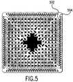
- FIG. 5shows exemplary routing in a substrate layer.
- FIG. 6illustrates a cross-sectional view of a die-up BGA package with heat spreader.
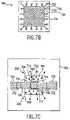
- FIG. 7Ashows a cross-sectional view of an example BGA package with an example heat sink assembly, according to an embodiment of the present invention.
- FIG. 7Bshows a top view of a first heat sink element of the heat sink assembly shown in FIG. 7A , according to an embodiment of the present invention.
- FIGS. 7C-7Eshow top views of the example BGA package of FIG. 7A with example heat sink assembly configurations, according to embodiments of the present invention.
- FIG. 7Fshows a cross-sectional view of a portion of an example BGA package, according to an embodiment of the present invention.
- FIGS. 7G and 7Hshow top views of example second heat sink elements, according to embodiments of the present invention.
- FIG. 8Ashows a cross-sectional view of an example BGA package with an example heat sink assembly, according to an embodiment of the present invention.
- FIGS. 8B and 8Cshow top views of the example BGA package of FIG. 8A with example heat sink assembly configurations, according to embodiments of the present invention.
- FIG. 8Dshows a cross-sectional view of an example BGA package with an example heat sink assembly, according to an embodiment of the present invention.
- FIG. 8Eshows a top view of the example BGA package of FIG. 8D with an example heat sink assembly configuration, according to embodiments of the present invention.
- FIG. 9Ashows a cross-sectional view of an example BGA package with an example perforated heat sink assembly, according to an embodiment of the present invention.
- FIG. 9Bshows a top view of the example perforated heat sink assembly of FIG. 9A , according to an embodiment of the present invention.
- FIGS. 9C and 9Dshow top views of example perforated heat sink assemblies, according to embodiments of the present invention.
- FIG. 10Ashows a cross-sectional view of an example BGA package with an example heat sink assembly, according to an embodiment of the present invention.
- FIG. 10Bshows a top view of the example heat sink assembly of FIG. 10A , according to an embodiment of the present invention.
- FIG. 11Ashows a cross-sectional view of an example BGA package with example heat sink assembly, according to an example embodiment of the present invention.
- FIG. 11Bshows an example surface of a first heat sink element of the example heat sink assembly of FIG. 11A that interfaces with an IC die through one or more passivation openings, according to an embodiment of the present invention.
- FIG. 11Cshows an example surface of a first heat sink element of the example heat sink assembly of FIG. 11A that interfaces with a second heat sink element of the example heat sink assembly, according to an embodiment of the present invention.
- FIG. 12shows an example segmented first heat sink element, according to an embodiment of the present invention.
- FIG. 13Ashows a cross-sectional view of an example BGA package with segmented heat sink assembly, according to embodiments of the present invention.
- FIGS. 13B-13Fshow example segmented heat sink assemblies, according to embodiments of the present invention.
- FIG. 14shows a cross-sectional view of an example BGA package with segmented heat sink assembly, according to embodiments of the present invention.
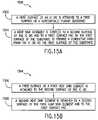
- FIGS. 15A and 15Bshow flowcharts that provide example steps for assembling embodiments of the present invention.
- the present inventionis directed to a method, system, and apparatus for improving the mechanical, thermal, and electrical performances of integrated circuit packages.
- the present inventionis applicable in land grid array (LGA), pin grid array (PGA), chip scale package (CSP), ball grid array (BGA), quad flat pack (QFP), and other integrated circuit package types.
- LGAland grid array
- PGApin grid array
- CSPchip scale package
- BGAball grid array
- QFPquad flat pack
- the present inventionis applicable to all types of package substrates, including ceramic, plastic, and tape (flex) substrates.
- the present inventionis applicable to die-up (cavity-up) and die-down (cavity-down) IC die orientations.
- the present inventionis described herein as being implemented in a BGA package.
- the present inventionis applicable to the other integrated circuit package types mentioned herein, and to additional integrated circuit package types.
- Ball grid array package typesare described below. A discussion of package inductances and resistances is then provided. Various embodiments of the present invention are also presented below. The embodiments described herein may be combined in any applicable manner, as required by a particular application.
- a ball grid array (BGA) packageis used to package and interface an IC die with a printed circuit board (PCB).
- BGA packagesmay be used with any type of IC die, and are particularly useful for high speed ICs.
- solder padsdo not just surround the package periphery, as in chip carrier type packages, but cover the entire bottom package surface in an array configuration.
- BGA packagesare also referred to as pad array carrier (PAC), pad array, land grid array, and pad-grid array packages.
- PACpad array carrier
- BGA package typesare further described in the following paragraphs. For additional description on BGA packages, refer to Lau, J. H., Ball Grid Array Technology , McGraw-Hill, New York, (1995), which is herein incorporated by reference in its entirety.
- die-up and die-down BGA package configurationsexist.
- the IC dieis mounted on a top surface of the substrate or stiffener, in a direction away from the PCB.
- die-down BGA packagesthe IC die is mounted on a bottom surface of the substrate or stiffener, in a direction towards the PCB.
- FIG. 1Aillustrates a conventional flex BGA package 100 .
- Flex BGA package 100includes an IC die 102 , a tape substrate 104 , a plurality of solder balls 106 , and one or more wire bonds 108 .
- Tape or flex BGA packagesare particularly appropriate for large IC dies with large numbers of input and outputs, such as application specific integrated circuits (ASIC) and microprocessors.
- ASICapplication specific integrated circuits
- Tape substrate 104is generally made from one or more conductive layers bonded with a dielectric material.
- the dielectric materialmay be made from various substances, such as polyimide tape.
- the conductive layersare typically made from a metal, or combination of metals, such as copper and/or aluminum. Trace or routing patterns are made in the conductive layer material.
- Substrate 104may be a single-layer tape, a two-layer tape, or additional layer tape substrate type. In a two-layer tape, the metal layers sandwich the dielectric layer, such as in a copper-Upilex-copper arrangement.
- IC die 102is attached directly to substrate 104 , for example, by an epoxy or other die-attach material.
- IC die 102is any type of semiconductor integrated circuit, separated from a semiconductor wafer.
- Bond pads 118are I/O pads for IC die 102 that make internal signals of IC die 102 externally available.
- Encapsulating material 116covers IC die 102 and wire bonds 108 for mechanical and environmental protection.
- Encapsulating material 116is a mold compound, epoxy, or other applicable encapsulating substance.
- flex BGA package 100does not include a stiffener.
- a stiffenercan be attached to the substrate to add planarity and rigidity to the package.
- FIG. 1Billustrates a flex BGA package 110 , similar to flex BGA package 100 , that incorporates a stiffener 112 .
- Stiffener 112may be laminated to substrate 104 .
- Stiffener 112is typically made from a metal, or combination of metals, such as copper, tin, and/or aluminum, or may be made from a polymer, for example.
- Stiffener 112also may act as a heat sink, and allow for greater heat spreading in BGA package 110 .
- One or more openings 114 in stiffener 112may be used to allow for wire bonds 108 to connect IC die 102 to substrate 104 .
- Stiffener 112may be configured in other ways, and have different opening arrangements than shown in FIG. 1B .
- FIG. 2Ashows a top view of a stiffener 112 .
- Stiffener 112includes an opening 114 adjacent to all four sides of an IC die mounting position 202 in the center of stiffener 112 .
- FIG. 2Bshows a temperature distribution 204 of a stiffener, such as stiffener 112 , during operation of an IC die in a flex BGA package. Temperature distribution 204 shows that heat transfer from IC die mounting position 202 to the edges of stiffener 112 is substantially limited by openings 114 . Openings 114 act as thermal barriers to heat spreading in stiffener 112 .
- FIG. 2Cshows a top view of an alternative configuration for stiffener 112 , according to an embodiment of the present invention.
- Stiffener 112includes an opening 206 adjacent to all four sides of an IC die mounting position 202 in the center of stiffener 112 . Openings 206 are similar to openings 114 of FIG. 2A , but of different shape. The different shape can enhance thermal transfer to the outer areas of stiffener 112 , for example. Further alternatively shaped openings in stiffener 112 are applicable to the present invention, including elliptical or rounded openings, etc.
- FIGS. 3A and 3Bshow cross-sectional views of conventional die-up PBGA packages 300 .
- PBGA package 300 shown in FIG. 3Aincludes a plastic substrate 302 , an IC die 304 , a plurality of solder balls 306 , a plurality of wire bonds 308 , a die pad 310 , one or more vias 314 , and one or more thermal/ground vias 316 .
- Plastic substrate 302includes one or more metal layers formed on an organic substrate (for example, BT resin or FR 4 epoxy/glass).
- IC die 304is mounted to die pad 310 .
- Wire bonds 308couple signals of IC die 304 to contact pads on the top surface of substrate 302 .
- An encapsulate material 320covers IC die 304 and wire bonds 308 for mechanical and environmental protection.
- encapsulate material 320may be a mold compound, epoxy, or other encapsulating substance.
- Solder balls 306are formed on solder ball pads on the bottom surface of substrate 302 . The solder ball pads are electrically coupled through substrate 302 to the contact pads on the top surface of substrate 302 .
- thermal/ground vias 316connect die pad 310 to one or more thermal/ground balls 322 on the center bottom surface of substrate 302 .
- IC die 304may be attached to die pad 310 with a die attach material 324 .
- die attach material 324may be an epoxy, such as a silver-filled epoxy, an adhesive tape, or other adhesive material.
- Wire bonds 308connect signals of IC die 304 to contact pads 326 of substrate 302 .
- Contact pads 326may be portions of bond fingers, traces, and pads accessible on the top surface of substrate 302 .
- gold bonding wireis bonded from aluminum bond pads on IC die 304 to gold-plated contact pads 326 on substrate 302 .
- the contact pads 326 on substrate 302connect to solder balls 306 attached to solder ball contact pads 328 the bottom surface of substrate 302 , through vias 314 and routing within substrate 302 using copper or other metal type conductors 312 .
- PBGA package 300 shown in FIG. 3Bdoes not include thermal/ground balls 322 .
- a BGA packageincludes an array of solder balls pads located on a bottom external surface of the package substrate for attachment of solder balls.
- FIG. 4Aillustrates a cross-sectional view of a die-up BGA package 400 .
- FIGS. 4B and 4Cillustrate exemplary solder ball arrangements for die-up BGA package 400 .
- BGA package 400includes an IC die 408 mounted on a substrate 412 .
- IC die 408is electrically connected to substrate 412 by one or more wire bonds 410 .
- Wire bonds 410are electrically connected to solder balls 406 underneath substrate 412 through corresponding vias and routing in substrate 412 .
- the vias in substrate 412can be filled with a conductive material, such as solder, to allow for these connections.
- Solder balls 406are attached to substrate 412 , and are used to attach the BGA package to a PCB.
- wire bondssuch as wire bonds 410
- IC diesmay be flipped and mounted to a substrate by solder balls located on the bottom surface of the IC die, by a process commonly referred to as “C4” or “flip chip” packaging.
- solder balls 406may be arranged in an array.
- FIG. 4Bshows a 14 by 14 array of solder balls on the bottom surface of BGA package 400 .
- Other sized arrays of solder ballsare also applicable to the present invention.
- Solder balls 406are reflowed to attach BGA package 400 to a PCB.
- the PCBmay include contact pads to which solder balls 406 are bonded.
- PCB contact padsare generally made from a metal or combination of metals, such as copper, nickel, tin, and/or gold.
- FIG. 4Cshows a bottom view of BGA package 400 , with an alternative solder ball array arrangement.
- BGA package 400attaches an array of solder balls 406 on a bottom surface of substrate 412 .
- solder balls 406are located in a peripheral area of the bottom surface of substrate 412 , away from a substrate center 424 .
- solder balls 406 on the bottom surface of substrate 412may be located outside an outer profile area of an IC die mounted on the opposite surface of substrate 412 .
- the solder ball arraymay be organized in any number of ways, according to the requirements of the particular BGA package application.
- the present inventionis applicable to any configuration or matrix of solders balls pads and solder balls, including full matrix, peripheral balls, center balls, etc.
- the BGA package substrateprovides vias and routing on one or more layers to connect contact pads for wire bonds on its upper surface to solder balls attached to the bottom substrate surface.
- FIG. 5shows an example routing 504 in a substrate layer 502 for accomplishing this.
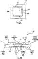
- FIG. 6shows a BGA package 300 , that includes a heat spreader 602 coupled to the top surface of substrate 302 .
- Heat spreader 602improves heat dissipation from BGA package 300 .
- Heat spreader 602conducts heat from the top surface of IC die 304 away from BGA package 300 to the environment. However, there is a gap 604 between heat spreader 602 and IC die 304 , and hence, heat does not efficiently conduct from IC die 304 to heat spreader 602 .
- the present inventionas described herein, provides for improved thermal performance in a BGA package.
- Ground and power wire bondsmay be coupled to respective ground and power rings on the surface of the BGA package substrate.
- Such ground and power ringscan often improve BGA package electrical performance by reducing BGA package inductances, and by saving space for signal input and output (I/O) wire bond connections.
- a ground ringis placed near to the IC die to reduce resistance and inductance of wire bonds so as to reduce ground bounce.
- One or more power rings for various supply voltagescan be placed on the substrate surface further away from the IC die.
- Signal bond fingersare placed outside of the outermost power/ground ring, spaced according to applicable design rules/constraints.
- Various planes, traces, and viasare integrated in the substrate to connect ground and power voltages, and other signals, to the corresponding solder balls on the bottom substrate surface.
- wire bondsmay be manufactured from expensive material, such as gold, and hence may be expensive. Hence, shorter wire bonds may be advantageous from a cost perspective also.
- ground and power ringsthat may be used on a BGA package substrate is limited by a maximum wire bond length and by a power/ground ring spacing requirement. Frequently, more power supply voltages are required by some IC dies, such as modem IC dies, than can be accommodated on a single substrate.
- power supply voltage levelsare being decreased.
- typical digital core power supply levelshave been reduced to 1.2-1.0 V for 0.13 ⁇ m wafer technology.
- a low power supply voltage valuerequires lower BGA package voltage drops for the IC die to operate properly.
- BGA package inductances and resistancesare related to the length of wire bonds, and longer wire bonds can lead to increased voltage drops.
- IC die clock and I/O data transfer frequenciesare increasingly becoming higher.
- the rise times for signal currentsare becoming shorter, and the rate of change of signal currents is becoming higher.
- IC dies having short current signal rise times, high change rates for signal currents, and low power supply voltage valueshave much more stringent restrictions on acceptable BGA package voltage level drops (including voltage drops due to package inductance and resistance).
- the present inventionis applicable to improving thermal and electrical performance in the BGA package types described herein, and further BGA package types.
- a package resistanceas well as inductance, may be lowered. This is especially important for power and ground signals. Reducing power and ground resistances and inductances may benefit the package in the following ways:
- Lower resistance and inductancewill reduce the core power supply droop.
- the lower resistancecan reduce the IR voltage drop and the lower inductance can reduce the voltage change due to core current change.
- Low resistance and low inductancewill benefit the IC die or chip when the core is operating at high or full speed.
- a typical signal path in a BGA packageincludes a bonding wire (i.e., wire bond), which connects the IC die or chip to a bond finger or ring on the surface of the substrate.
- the tracesare often replaced with corresponding conductive rings and planes.
- the total resistance and inductance of a signalmay be calculated by summing the resistance and inductance of each above-mentioned path portion, in a first grade approximation.
- Equation 1The voltage drop or ground bounce due to package inductance can be described by a simplified formula in Equation 1:
- Va change in voltage caused by the inductance
- Equation 1shows that the voltage drop is proportional to the package inductance L.
- Equation 2A partial self inductance (L) per unit length of a wire bond of a finite radius r, a length 1, permeability constants ⁇ 1 and ⁇ 2, and conducting a current i, is expressed in Equation 2 for low frequencies:
- Equation 21 i ⁇ ⁇ 0 a ⁇ ⁇ 1 ⁇ ir 2 ⁇ ⁇ ⁇ ⁇ r 2 ⁇ d r + ⁇ 0 ⁇ ⁇ ⁇ 2 ⁇ i 2 ⁇ ⁇ ⁇ ⁇ r ⁇ d r Equation ⁇ ⁇ 2
- Equation 3an external partial self inductance
- hthe distance from l to ground plane
- Equation 3shows that the inductance of a wire bond is proportional at the first level approximation to the wire length.
- Equation 4shows the inductance Lwires for a number n of wire bonds for a particular signal net:
- Ljthe inductance of a wire bond j.
- a total inductance Lpackageis equal to the sum of inductances for all wire bonds, for the substrate, and for the solder balls, as is expressed in Equation 5:
- L packageL wires +L substrate +L solderball Equation 5
- the present inventionprovides for improved thermal conduction from an IC die through a heat spreader, and provides for reduced package inductance.
- a heat sink assemblyis coupled to the IC die in a BGA package.
- the heat sink assembly of the present inventionmay also be referred to as a connection module.
- the heat sink assemblyprovides an enhanced thermal and electrical connection from the IC die to the package substrate.
- the heat sink assemblyforms a electrical connection path that can be used for ground, power and other critical signals.
- the first heat sink element and second heat sink elementmay be electrically segmented or divided to support a plurality of signals. Hence, any number of one or more signals may be electrically connected through the heat sink assembly, including ground, power, and other signals.
- the second heat sink elementis made of a metal or alloy, such as copper or aluminum, it has much lower inductance and resistance compared to conventional wire bonds. Hence, the second heat sink element significantly reduces the package voltage drop. Furthermore, the second heat sink element improves thermal dissipation from the IC die, by improving heat transfer to the environment. The first heat sink element further reduces the package inductance, and minimizes the voltage drop.
- Inner wire bonds used to bond IC die signals to the heat sink assemblyeffectively shorten the length of wire bonds for signals. As described above, shorter wire bonds greatly reduce the package inductance and resistance. Because the second heat sink element is made of a metal that is thicker than a wire bond, it reduces the package inductance and resistance further. Additionally, when the second heat sink element is used for ground, it can further reduce signal wire inductance by providing ground shielding.
- the first heat sink elementwhen formed with bumps to conform to an IC die with corresponding passivation openings, combines the advantages of wire bonding and a flip chip configuration.
- a very short signal pathis provided due to the close proximity of the first heat sink element bumps and IC die, which leads to a lower voltage drop.
- the thermal performance of the BGA package with heat sink assemblyis improved over that of conventional BGA packages due to the close proximity of the heat sink assembly to the IC die. They are coupled at the top surface of the IC die.
- the heat sink assemblymay include two- and single-heat sink elements.
- the single heat sink element embodimentscombine advantages of the two heat sink elements described herein.
- the single heat sink elementmay be configured to coupled to an IC die mounted in a standard configuration or a flip chip orientation, and in other ways described for two heat sink embodiments.
- single heat sink element packagesmay further be configured in additional ways, as described herein.
- FIG. 7Aillustrates a cross-sectional view of a BGA package 700 that includes a heat sink assembly 702 , according to an embodiment of the present invention.
- FIG. 7Cshows a top view of BGA package 700 , without encapsulate material 320 and some surface features of substrate 302 visible.
- BGA package 700is substantially similar to the BGA packages described above, subject to the differences described below.
- Heat sink assembly 702includes a first heat sink element 704 and a second heat sink element 706 , according to an embodiment of the present invention.
- First heat sink element 704may also be referred to as an “inner connector,” and second heat sink element 706 may also be referred to as an “outer connector.”
- First and second heat sink elements 704 and 706contribute to the thermal, electrical, and mechanical advantages of the present invention.
- First heat sink element 704is attached to the top surface of IC die 304 by an adhesive layer 710 .
- Adhesive layer 710may also act as a cushion layer to absorb an impact force that occurs during a wire bonding process, when wire bonds are attached to first heat sink element 704 .
- Adhesive layer 710may be an epoxy or adhesive film, or other adhesive material. In some applications, an adhesive thin film may provide relative ease in attachment to IC die 304 , and a beneficial cushion effect.
- adhesive layer 710is a thermally conductive adhesive material, to enable thermal transfer from IC die 304 to heat sink assembly 702 .
- Adhesive layer 710may or may not be electrically conductive, depending on the particular application.
- Adhesive layer 714mechanically, thermally, and/or electrically couples first heat sink element 704 and second heat sink element 706 .
- Adhesive layer 714is typically an electrically and thermally conductive layer that couples first heat sink element 704 and second heat sink element 706 .
- Materials that may be used for adhesive layer 714include conductive epoxy (e.g., silver-filled), conductive film, and other thermally and electrically conductive adhesive materials.
- a conductive tape or filmmay be used for adhesive layer 714 . When used, the conductive film may be placed on the top surface of first heat sink element 704 .
- a thermal compression bonding processmay be used to bond second heat sink element 706 firmly to first heat sink element 704 using the conductive film.
- adhesive layer 714may be electrically and/or thermally non-conductive, depending on the particular application.
- An adhesive layer 716mechanically, thermally, and/or electrically couples second heat sink element 706 to an exposed contact pad 720 of substrate 302 .
- Materials that may be used for adhesive layer 716include conductive epoxy (e.g., silver-filled), conductive film, and other thermally and/or electrically conductive adhesive materials.
- Contact pad 720may be a metal pad, ring, trace, or other land type contact, for example.
- One or more vias 314 , traces or planes in substrate 302are used to electrically couple contact pad 720 to one or more corresponding solder balls 306 .
- the corresponding solder ballsare attached to the bottom surface of substrate 302 directly beneath contact pad 720 . This may allow for a shortest electrical path for the respective signal, and lowest resistance and/or inductance. In other embodiments, however, the corresponding solder balls 306 may be located elsewhere on the bottom surface of substrate 302 .
- a top surface of first heat sink element 704is wire bondable in a peripheral region, and is electrically conductive in a center region.
- FIG. 7Bshows a top surface of first heat sink element 704 , according to an embodiment of the present invention.
- bond pads 722 and a contact area 724are formed on the top surface of heat sink element 704 .
- Bond pads 722may be bond fingers, pads, areas, rings, or other bond pad types.
- Bond pads 722 and contact area 724are electrically conductive, and may be formed from conductive metals formed in or plated on first heat sink element 704 , for example. Bond pads 722 are electrically coupled to contact area 724 by traces 726 .
- Second heat sink element 706is electrically coupled to contact area 724 when attached to first heat sink element 704 by adhesive layer 716 . Hence, when wire bonds from IC die 304 are bonded to bond pads 722 , they are electrically coupled to second heat sink element 706 through trace 726 and contact area 724 .
- inner wire bonds 708couple IC die bond pads 712 inwardly to the peripheral region of first heat sink element 704 .
- inner wire bonds 708are standard wire bonds.
- Inner wire bonds 708can be attached or bonded between IC die 304 and first heat sink element 704 during the same manufacturing step as are other BGA package wire bonds, such as wire bonds 308 .
- Inner wire bonds 708may alternatively be applied during a separate manufacturing step.
- Inner wire bonds 708can be bonded from either inner or outer rows of staggered bond pads 712 on IC die 304 , for example. As shown in FIG. 7C , wire bonds 708 are bonded to bond pads 722 of first heat sink element 704 .
- adhesive layer 710may effectively absorb the impact force created when inner wire bonds 708 are applied to first heat sink element 704 , and can aid in protecting the integrity of IC die 304 .
- a combination of inner wire bonds 708 , first heat sink element 704 , adhesive layer 714 , second heat sink element 706 , adhesive layer 716 , and contact pad 720allow for ground, power and/or other signals to be electrically coupled from IC die 304 to substrate 302 , and hence to one or more corresponding solder balls 306 .
- first heat sink element 704is substantially planar, and may be rectangular, rounded, or otherwise shaped.
- First heat sink element 704may be formed from a variety of materials, including a printed circuit board (PCB) substrate, a metal or alloy, silicon, and/or a single- or multi-layer tape. Example embodiments for each of these configurations of first heat sink element 704 are further described as follows.
- PCBprinted circuit board
- A) PCB substrate materialA single- or multi-layer PCB substrate is suitable for use as first heat sink element 704 .
- PCB substrate materialsare especially useful when necessary to connect more than one signal net through heat sink assembly 702 .
- bond pads or fingers for a same-signal netare coupled together in the PCB substrate of heat sink element 704 , and are connected to a particular contact area of second heat sink element 706 .
- Second heat sink element 706may be segmented into two or more portions in order to couple different electrically isolated contact areas of first heat sink element 704 to corresponding contact pads of substrate 302 .
- a metalmay be used for first heat sink element 704 to improve thermal performance.
- first heat sink element 704may include copper, aluminum, tin, lead, gold, silver, nickel, or other metals, or combinations or alloys thereof.
- a standard lead frame materialsuch as C7025 or EFTEC may be used.
- Inner wire bonds 708are bonded to peripheral wire bondable plated pads or areas on first heat sink element 704 .
- a single or multi-layer tapemay be used for first heat sink element 704 .
- a two-layer tapemay be conveniently used. With an adhesive layer already attached on the back side of the tape, a tape first heat sink element 704 may be easily attached to IC die 304 .
- a silicon piece or chip similar to IC die 304 , with connecting circuits formed thereon,may be used as a first heat sink element 704 .
- inner wire bonds 708are bonded from bond pads 712 on IC die 304 to bond pads on the silicon first heat sink element 704 .
- first heat sink element 704is suitable for first heat sink element 704 .
- Second heat sink element 706may be manufactured from a variety of materials, depending on the electrical and thermal performance desired.
- a metalmay be used for second heat sink element 706 to improve thermal and electrical performance.
- second heat sink element 706may include copper, aluminum, tin, lead, gold, silver, nickel, or other metals, or combinations or alloys thereof.
- Second heat sink element 706may also be manufactured from ceramic, graphite, plastic, and/or other materials.
- I/O bond pads of IC die 304may be simultaneously coupled by wire bonds to substrate 302 and by inner wire bonds 708 to heat sink assembly 702 .
- heat sink assembly 702may be removed from the BGA package for failure analysis, for example, while IC die 304 is still capable of operating.
- Second heat sink element 706may be shaped in a variety of ways, to allow connection between first heat sink element 704 and substrate 302 . As shown in FIG. 7A , second heat sink element 706 is formed such that one or more of its ends 718 are allowed to contact substrate 302 .
- FIG. 7Fshows an cross-sectional view of a portion of an example BGA package 700 attached to an example PCB 750 , according to an embodiment of the present invention.
- second heat sink element 706can be viewed as having a central region 730 (a portion of which is shown in FIG. 7F ) and one or more arms 732 that extend from central region 730 to contact substrate 302 .
- a bottom surface of central region 730is coupled to the top surface of first heat sink element 704 .
- central region 730is substantially planar.
- central region 730is recessed. Note that in alternative embodiments, as described below, central region 730 does not have to be recessed.
- arm 732has a first arm portion 734 and a second arm portion 736 coupled in series.
- First arm portion 734extends from central region 730 in an upward direction to allow arm 732 to avoid contact with inner wire bond 708 and wire bond 308 .
- Second arm portion 736extends in a downward direction to allow arm 732 to couple with contact pad 720 on the top surface of substrate 302 .
- this configurationforms an M-shaped cross-section for second heat sink element 706 .
- FIG. 7Gshows second heat sink element 706 of FIG. 7A in further detail.
- second heat sink element 706has first and second arms 732 a and 732 b .
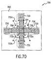
- FIGS. 7D , 7 E, and 7 Hshow further example shapes for second heat sink element 706 , from a top view, according to example embodiments of the present invention.
- second heat sink element 706has first, second, third, and fourth arms 732 a - 732 d .
- Second heat sink element 706may have any number of one or more arms, as is required by the particular application.
- second heat sink element 706may be thought of as having an arm 732 with a width that is continuous around central region 730 .
- contact pad 720is a continuous ring on the top surface of substrate 302 .
- Contact pad 720may also be separated into a plurality of contact pads in the configuration shown in FIG. 7E .
- second heat sink element 706is coupled to four circular contact pads 720 a - 720 d at corresponding corners or ends 718 a - d of second heat sink element 706 .
- the corners or ends 718 a - d of second heat sink element 706are formed in squared or “cut off” shape.
- Second arm portions 736 a - 736 d of second heat sink element 706are bent, stamped, molded, or otherwise formed so that ends 718 a - d make contact with contact pads 720 a - d .
- the number of contact pads 720may alternatively be greater or less than four, depending on the particular application.
- second heat sink 706is a relatively large plane that covers a large portion of the top surface of substrate 302 . In this manner, second heat sink 706 is able to transfer more heat from IC die 304 to the environment.
- Second heat sink element 706may have alternative and additional shapes, as would be understood to persons skilled in the relevant art(s) from the teachings herein.
- heat sink assembly 702includes a single heat sink element.
- FIGS. 8A and 8Deach illustrate BGA package 700 with heat sink assembly 702 , according to single heat sink element embodiments of the present invention.
- heat sink assembly 702includes a single-piece heat sink element that couples one or more signal nets of IC die 304 to substrate 302 , in a similar fashion to that described for the two heat sink element embodiments described above.
- the single-piece heat sink element of the embodiments of FIGS. 8A and 8Dincludes benefits of both of first heat sink element 704 and second heat sink element 706 , in a single piece.
- the single heat sink element or connector element of heat sink assembly 702is heat sink element 802 .
- Heat sink element 802may be made from materials such as those from which first and second heat sink elements 704 and 706 may be made.
- Heat sink element 802is preferably made from a metal material, with wire bondable plated areas 818 for attachment of inner wire bonds 708 .
- Heat sink element 802includes one or more formed portions or arms 806 that extend towards substrate 302 from a central region 814 for attachment to substrate 302 , similarly to second heat sink element 706 . In the embodiment shown in FIG. 8A , first and second arms 806 a and 806 b are shown.
- Arms 806may be formed to conform relatively closely to IC die 304 , to attach to substrate 302 at exposed contact pads 808 relatively closely to IC die 304 .
- contact pads 808may be metal rings, traces, bond fingers, and other lands that are formed on substrate 302 .
- heat sink element 802may be shaped in a variety of ways.
- FIGS. 8B and 8Cshows example top views of BGA package 700 , with heat sink element 802 , according to embodiments of the present invention.
- Heat sink element 802may have any number of one or more arms 806 .
- FIG. 8Bshows heat sink element 802 with four arms 806 a - 806 d , with two arms 806 extending to the substrate on each of two sides of IC die 304 .
- FIG. 8Cshows heat sink element 802 with four arms 806 a - 806 d , with a single arm 806 extending to the substrate on each of the four sides of IC die 304 .
- the single heat sink element of heat sink assembly 702includes a single heat sink element 804 .
- Heat sink element 804may be made from materials such as those from which first and second heat sink elements 704 and 706 may be made.
- Heat sink element 804is preferably made from a metal material, with wire bondable plated areas for attachment of inner wire bonds 708 .
- Heat sink element 804includes one or more formed portions or arms 810 that extend towards substrate 302 from a central region 816 for attachment to substrate 302 .
- first and second arms 810 a and 810 bare shown.
- Arms 810may be formed to extend relatively far from IC die 304 on substrate 302 , similarly to the structure of second heat sink element 706 shown in FIG. 7A , for example. Arms 810 attach to substrate 302 at exposed contact pads 812 , which are substantially similar to contact pads 808 of FIG. 8A .
- heat sink element 804may be shaped in a variety of ways.
- FIG. 8Eshows an example top view of BGA package 700 , with heat sink element 804 , according to an embodiment of the present invention.
- Heat sink element 804is applicable to being shaped as elsewhere shown herein for other heat sink elements, including in the manner shown for second heat sink element 706 as shown in FIGS. 7A-7G .
- heat sink element 804may be formed to have a M-shaped cross-section, as shown in FIG. 8D , or may be otherwise formed.
- a conductive epoxymay be dispersed on the top surface of first heat sink element 704 as adhesive layer 710 , and then second heat sink element 706 may be placed on first heat sink element 704 .
- the conductive epoxyis typically cured after placing second heat sink element 706 on first heat sink element 704 .
- second heat sink element 706may be perforated.
- FIG. 9Ashows a cross-sectional view of a BGA package 700 that includes a second heat sink element 706 with one or more perforations 902 , according to an embodiment of the present invention.
- FIG. 9Bshows a top view of second heat sink element 706 of FIG. 9A .
- the perforated second heat sink element 706may have perforations 902 in center region 730 of the top surface of second heat sink element 706 .
- a conductive epoxy 906may be applied to center region 730 of the top surface of second heat sink element 706 , to fill in perforations 902 in second heat sink element 706 .
- Conductive epoxy 906may be used alternatively to, or combined with adhesive layer 714 to better thermally, mechanically, and/or electrically couple second heat sink element 706 to first heat sink element 704 .
- Second heat sink element 706may be additionally or alternatively perforated in other portions.
- FIGS. 9C and 9Dshow top views of second heat sink element 706 , according to further embodiments of the present invention.
- Second heat sink element 706may have perforations in one or more ends 718 .
- second heat sink element 706has perforations 908 in first and second ends 718 a and 718 b .
- Second heat sink element 706may also have perforations in any portion of one or more arms 732 .
- second heat sink element 706has perforations 904 in first and second arms 732 a and 732 b.
- Perforations 902 , 904 , and 908can increase a contacting area and improve reliability.
- Perforations 902enhance an electrical, thermal, and mechanical connection between first heat sink element 704 and second heat sink element 706 .
- Perforations 908enhance an electrical, thermal, and mechanical connection between second heat sink element 706 and respective contact pads 720 on substrate 302 .
- Perforations 902 and 908allow an excess adhesive material, such as an epoxy, to flow through them while bonding second heat sink element 706 to first heat sink element 704 and contact pad 720 , respectively. Hence, the adhesive material does not spread as much horizontally, and adhesiveness between second heat spreader 704 and first heat sink element 704 and/or contact pad 720 is improved.
- Perforations 904provides for enhanced bonding between second heat sink element 706 and encapsulate material 320 , and for void free encapsulation.
- a molding compound applied to a BGA packagewill have improved interfacial bonding to second heat sink element 706 with perforations 904 .
- the molding compound at the top and bottom surfaces of second heat sink element 706is allowed to join together through perforations 904 , improving the adhesion of the molding compound to second heat sink element 706 and the BGA package.
- perforations 904allow the molding compound to flow through second heat sink element 706 into “voids” or spaces under second heat sink element 706 that would be difficult or impossible for the molding compound to reach if it could only flow in from the sides of second heat sink element 706 .
- first heat sink element 704 and single heat sink elements 802 and 804may also be perforated as described above, to provide similar benefits.
- second heat sink element 706a specific portion of second heat sink element 706 may be left perforation-free, such as the geometrical center of heat sink element 706 . This perforation-free location may allow a pick and place device to better attach to second heat sink element 706 .
- Second heat sink element 706 or single heat sink elements 802 and 804may be completely encapsulated in BGA package 700 by encapsulate 320 , such as shown in FIG. 9 for second heat sink element 706 .
- a portion 1002 of second heat sink element 706 (or single heat sink element 802 or 804 )may be exposed through encapsulate 320 , as shown in FIG. 10A , according to an embodiment of the present invention.
- FIG. 10Bshows a top view of second heat sink element 706 of FIG. 10A .
- central region 730 of second heat sink element 706 (or single heat sink element 802 )is not recessed.
- second heat sink element 706may be considered to be substantially planar in portion 1002 on its top surface, with a protruding portion 1004 on its bottom surface.
- Protruding portion 1004is coupled to first heat sink element 704 .
- protruding portion 1004may be a piece separate from first and second heat sink elements 704 and 706 , that is coupled between first and second heat sink elements 704 and 706 .
- the separate-piece protruding portion 1004may be made of any of the materials that first and second heat sink elements 704 and 706 may be made of, and other materials.
- An electrically and/or thermally conductive adhesive materialmay be used to attach the separate-piece protruding portion 1004 to first and second heat sink elements 704 and 706 .
- FIG. 11Ashows an example configuration for BGA package 700 , according to an embodiment of the present invention.
- I/O pads of IC die 304are electrically accessed by heat sink assembly 702 through the top surface of IC die 304 .
- first heat sink element 704may be a PCB or tape substrate that is bumped with one or more conductive bumps 1102 .
- bumps 1102may be gold, silver, aluminum, copper, other metal, or alloys or combinations of metals, or other conductive materials.
- a plurality of bumps 1102may be arranged to form a pattern or matrix on the bottom surface of first heat sink element 704 .
- FIG. 11Bshows the bottom surface of first heat sink element 704 , according to an embodiment of the present invention. As shown in FIG. 11B , the bottom surface of first heat sink element 704 has a plurality of bumps 1102 , formed in an example pattern.
- IC die 304may be formed to have a corresponding pattern or matrix of passivation openings in its top surface to match the bumps 1102 of first heat sink element 704 .
- one or more ground, power, and/or signal nets of IC die 304can be electrically coupled to first heat sink element 704 by coupling of bumps 1102 to the signals exposed in the corresponding openings on the upper surface of IC die 304 .
- the matching patterns or matricescan enhance the thermal, electrical, and mechanical coupling of first heat sink element 704 to IC die 304 .
- First heat sink element 704can be bonded to IC die 304 using a thermal compression process, for example.
- Inner wire bonds 708may also be present, but are not required in the embodiment for BGA package 700 shown in FIG. 11A .
- FIG. 11Cshows the top surface of first heat sink element 704 , corresponding to the bottom surface of first heat sink element 704 shown in FIG. 11B , according to an example embodiment of the present invention.
- the bottom surface of first heat sink element 704has an electrically conductive contact area 1106 .
- One or more bumps 1102are electrically coupled to contact area 1106 in first heat sink element 704 , using conductive vias, etc.
- Second heat sink element 706is electrically coupled to contact area 1106 when attached to first heat sink element 704 as described above, to electrically couple the one or more ground, power, and/or signal nets of IC die 304 to second heat sink element 704 .
- contact area 1106may be segmented into a plurality of electrically isolated contact areas to support multiple ground, power, and/or signal nets of IC die 304 .
- single heat sink elements 802 and 804may be formed with one or more bumps 1102 to interface with I/O pads of IC die 304 in a single heat sink element embodiment.
- single heat sink elements 802 or 804may each be configured to directly interface with signals of IC die 304 through passivation openings in the IC die 304 .
- a total parts countis reduced, and construction of the integrated circuit package is simplified.
- the present inventionis applicable to any number of ground, power, and signal nets being coupled to segmented portions of heat sink assembly 702 .
- two signal netscan be bonded to first heat sink element 704 , such as ground and power.
- Electrically separate bond fingersare formed on first heat sink element 704 .
- Ground and power I/O pads of IC die 304are coupled to the electrically separate bond fingers.
- the bond fingers of first heat sink element 704can be designed such that ground and power bond fingers have substantially the same length, and are placed next to each other.
- FIG. 12shows an example of first heat sink element 704 that is divided or segmented to allow for connection with a plurality of signals, according to an embodiment of the present invention.
- FIG. 12shows two contact area segments, first contact area 1202 and second contact area 1204 , that each correspond to a different signal net.
- First and second contact areas 1202 and 1204are exposed on the top surface of first heat sink element 704 for attachment to respective segmented portions of second heat sink element 706 .
- inner wire bonds 708are bonded to one or more bond pads or fingers of first heat sink element 704 . Bond pads or fingers of one signal value are coupled internally in first heat sink element 704 to one of first and second contact areas 1202 and 1204 .
- first bond fingers 1206are coupled to first contact segment 1202
- second bond fingers 1208are coupled to second contact segment 1204
- ground I/O pads of IC die 304may be coupled to one or more of first bond fingers 1206
- power I/O pads of IC die 304may be coupled to one or more of second bond fingers 1208 .
- FIG. 13Ashows a cross-sectional view of BGA package 700 that includes a segmented heat sink assembly 702 , according to an embodiment of the present invention.
- Heat sink assembly 702includes a segmented second heat sink element 706 , that has a first segment 1302 a and a second segment 1302 b .
- first segment 1302 aincludes a first arm and a first portion of the central region of second heat sink element 706
- second segment 1302 bincludes a second arm and a second portion of the central region of second heat sink element 706 .
- First segment 1302 a and second segment 1302 bare electrically insulated from each other, by an insulator 1306 .
- First segment 1302 ais coupled to a first contact area of first heat sink element 704 , such as first contact area 1202
- second segment 1302 bis coupled to a second contact area of first heat sink element 704 , such as second contact area 1204 .
- first segment 1302 a and the first contact area of first heat sink element 704allows for a first signal to be electrically coupled to substrate 302 with low inductance and resistance.
- second segment 1302 b and the second area of first heat sink element 704allows for a second signal to be electrically coupled to substrate 302 with low inductance and resistance.
- the first and second signalsare electrically isolated.
- Heat sink assembly 702may be segmented in a variety of ways.
- FIGS. 13B-13Dshow examples of segmented versions of second heat sink element 706 , according to embodiments of the present invention.
- FIG. 13Bshows a segmented version of second heat sink element 706 , with first and second segments 1302 a and 1302 b , that would be suitable for use with the segmented first heat sink element 704 shown in FIG. 12 .
- FIG. 13Cshows a segmented version of second heat sink element 706 with four segments 1302 a - 1302 d .
- FIG. 13Dshows a cross-shaped segmented version of second heat sink element 706 with four segments 1302 a - 1302 d.
- FIGS. 13E and 13Fshow top views of BGA package 700 , according to another segmented embodiment for heat sink assembly 702 .
- FIG. 13Eshows a segmented first heat sink element 704 attached to IC die 304 in BGA package 700 .
- FIG. 13Fshows a segmented second heat sink element 706 attached to the segmented first heat sink element 704 of FIG. 13E .
- first heat sink element 704has four contact areas 1304 a - d , for electrical coupling with second heat sink element 706 .
- the top surface of substrate 302has eight contact pads 720 a - 720 h for coupling with second heat sink element 706 .
- a ground ring 1306surrounds IC die 304 .
- Wire bonds(not shown in FIG. 13E ) are coupled between I/O pads of IC die 304 and ground ring 1306 , and between I/O pads of IC die 304 and bond fingers/traces on the top surface of substrate 302 .
- inner wire bonds(not shown in FIG.
- first heat sink element 704may be coupled between I/O pads of IC die 304 and bond pads/fingers on the top surface of first heat sink element 704 .
- inner wire bondsare not present, and first heat sink element 704 is electrically coupled to one or more signals in IC die 304 through one or more passivation openings in the top surface of IC die 304 .
- segmented second heat sink element 706includes first and second segments 1302 a and 1302 b .
- First and second segments 1302 a and 1302 bare each similar to second heat sink element 706 shown in FIG. 7H , and include perforations 902 , 904 , and 908 .
- First and second segments 1302 a and 1302 bare coupled between first heat sink element 704 and contact pads 720 a - h .
- first and second segments 1302 a and 1302 bprovide an electrical and/or thermal path between IC die 304 and contact pads 720 a - h .
- first segment 1302couples contact areas 1304 a and 1304 b to contact pads 720 a - d
- second segment 1304couples contact areas 1304 c and 1304 d to contact pads 720 e - h.
- perforations 902enhance connection of first and second segments 1302 a and 1302 b to contact areas 1304 a - d , as described above with reference to FIG. 9B .
- Perforations 904enhance connection of an encapsulate material 320 (not shown in FIGS. 13E and 13F ) to second heat sink element 706 , as described above with reference to FIG. 9D .
- Perforations 908enhance connection of second heat sink element 706 to contact pads 720 a - h , as described above with reference to FIG. 9C .
- Second heat sink element 706may be segmented in any number of ways, as would be understood by persons skilled in the relevant art(s). First heat sink element 704 will be correspondingly segmented, to support electrical coupling and electrical isolation, as required by the particular segmented configuration of second heat sink element 706 . When segmented, the separate segments of second heat sink element 706 may be attached to a BGA package separately, or they may be pre-joined, by insulator 1306 or other attachment mechanism, and then attached to the BGA package as a unit. Note that in some configurations, when second heat sink element 706 is segmented, a thermal stress on IC die 304 may be reduced relative to a thermal stress when second heat sink element 706 is not segmented. For example, the thermal stress may be reduced on the top surface of IC die 304 when the environmental temperature changes over a range such as from a low temperature to a high temperature, and vice versa.
- FIG. 14shows a cross-sectional view of an example of BGA package 700 , with a segmented heat sink element 804 , according to an embodiment of the present invention.
- Heat sink element 804includes a first segment 1402 and a second segment 1404 .
- First segment 1402 and second segment 1404are electrically insulated from each other, by insulator 1306 .
- Single heat sink element 802may be segmented in a variety of ways, including in the manner of the examples shown for second heat sink element 706 in FIGS. 13A-13D .
- the separate segments of single heat sink elements 802 and 804may be attached to a BGA package separately, or they may be pre-joined, by an insulator or other attachment mechanism, and then attached to the BGA package as a unit.
- first heat sink element 704may be segmented. Similarly to segmented second heat sink element 706 and segmented single heat sink elements 802 and 804 , a segmented first heat sink element 704 the separate segments of first heat sink element 704 may be attached to an IC die separately, or they may be pre-joined, by an insulator or other attachment mechanism, and then attached to the IC die as a unit.
- FIG. 15Ashows a flowchart 1500 providing steps for assembling one or more embodiments of the present invention.
- FIG. 15Bshows additional steps for assembling embodiments of the present invention.
- the steps of FIGS. 15A and 15Bdo not necessarily have to occur in the order shown, as will be apparent to persons skilled in the relevant art(s) based on the teachings herein. Other structural embodiments will be apparent to persons skilled in the relevant art(s) based on the following discussion. These steps are described in detail below.
- Flowchart 1500begins with step 1502 .
- a first surface of an IC dieis attached to a first surface of a substantially planar substrate.
- the IC dieis IC die 304
- the substrateis substrate 302 .
- IC die 304is attached to the top surface of substrate 304 .
- a heat sink assemblyis coupled to a second surface of the IC die and to a first contact pad on the first surface of the substrate to provide a conductive path from the IC die to the first surface of the substrate.
- the heat sink assemblyis heat sink assembly 702 .
- heat sink assembly 702is attached to the top surface of IC die 304 , and to contact pad 720 on the surface of substrate 302 .
- An electrically and/or thermally conductive pathis provided through heat sink assembly 702 to substrate 302 .
- Further examples of heat sink assembly 702 of the present inventionare shown in FIGS. 7C-7G , 8 A- 8 E, 9 A, 9 B, 10 A, 10 B, 10 A, 13 A- 13 D, and 14 .
- step 1504includes the step where an electrically conductive path is formed from a first I/O pad of said IC die to the first contact pad.
- a wire bond 712electrically couples an I/O pad 712 of IC die 304 to heat sink assembly 702 , which in turn electrically couples the I/O pad 712 to contact pad 720 .
- FIG. 11Ashows an embodiment, where a conductive bump 1102 of heat sink assembly 702 is electrically coupled to an I/O pad (not shown) of IC die 304 through a passivation opening. Heat sink assembly 702 , in turn, electrically couples the I/O pad to contact pad 720 .
- step 1504may include the steps shown in FIG. 15B .
- a first surface of a first heat sink elementis attached to the second surface of the IC die.
- the first heat sink elementis first heat sink element 704 shown in FIG. 7A .
- first heat sink element 704is attached to the top surface of IC die 304 .
- a second heat sink elementis attached to a second surface of the first heat sink element and to the first contact pad.
- the second heat sink elementis second heat sink element 706 .
- second heat sink element 706is attached to the top surface of first heat sink element 704 , and to contact pad 720 .
- step 1502may include the step where the IC die is mounted on a substrate, and first heat sink element 704 with pre-formed conductive bumps is mounted on the IC die in a flipped orientation.
- Step 1502may include the step where a conductive bump on a surface of the heat sink assembly is electrically coupled to an I/O pad of the IC die through a passivation opening in the second surface of the IC die, as described above.
- step 1504may include the step where a heat sink element is attached to the second surface of the IC die and to the first contact pad on the surface of the substrate.
- the single heat sink elementmay be single heat sink element 802 or 804 , shown in FIGS. 8A and 8B , respectively.
- heat sink element 802is coupled to the top surface of IC die 304 , and to contact pad 808 .
- heat sink element 804is coupled to the top surface of IC die 304 , and to contact pad 812 .
- Short wire bond lengthsreduce the inductance and resistance of the package. For example, in conventional BGA packages, ground rings are formed a particular distance from the IC die on the package substrate so that they are not contacted by an overflow of the IC die attach epoxy. Hence, an example minimum wire bond length for a ground signal is around 1.0 mm. According to the present invention, the inner wire bonds can be shorter because a ground ring can be formed on the first heat sink element. Furthermore, when an adhesive tape is used to attach the IC die to the first heat sink element, there is no concern for epoxy flow.
- a first heat sink element with metal bumps thereonallows for a more direct connection from the IC die core to the second heat sink element, thus reducing the voltage drop for core power.
- Additional power ringsBy removing a ring (e.g., a ground or power ring) from the package substrate, more area is available on the package substrate for additional substrate and rings. For example, an additional power ring may be formed on the package substrate.
- a ringe.g., a ground or power ring
- Shorter wire bondshave a lower inductance value, which helps to reduce the package voltage drop.
- the number of wire bondsis based on a calculated allowable voltage drop.
- the heat sink assembly of the present inventioncan significantly decrease the number of required wire bonds, making it easier to meet voltage drop requirements.
- Reduced required IC die sizeBecause the number of required power and/or ground wire bonds is reduced in the package of the present invention, the required IC die size can be decreased, because IC dies with fewer I/O pads may be used.
- the reduced wire bond lengths of the present inventionleads to improved performance of the I/O signals from the IC die. This is due to a number of factors, including lower inductance and resistance, less susceptibility to noise, decreased signal path distance, etc.
- one or more ringsmay be removed from the package substrate, there is more area on the package substrate to position bond fingers, vias, and traces for routing. Furthermore, more bond fingers may be positioned on the substrate with the same maximum wire bond length restriction.
- Reduced package body sizeA reduced package body size is possible because of the improved routability of the package, as described above.
- Fewer substrate layers requiredFewer substrate layers may be used because of the benefits of lower inductance and resistance, improved routability, and enhanced thermal performance described herein.
- Ground and/or power bond pads used for inner wire bond attachmentcan be placed at an inner row of bond pads on the IC die top surface. This greatly increases IC die design flexibility. For example, in conventional BGA packages, ground and power bond pads are often required to be placed at the outer row of IC die bond pads.
- the package of the present inventionoperates very efficiently to spread heat from the IC die.
- Second heat sink element 706effectively shields signals inside the package, and minimized electromagnetic interference (EMI).
- EMIelectromagnetic interference
Landscapes
- Engineering & Computer Science (AREA)
- Microelectronics & Electronic Packaging (AREA)
- Physics & Mathematics (AREA)
- Condensed Matter Physics & Semiconductors (AREA)
- General Physics & Mathematics (AREA)
- Computer Hardware Design (AREA)
- Power Engineering (AREA)
- Cooling Or The Like Of Semiconductors Or Solid State Devices (AREA)
Abstract
Description
Where:
The left-most integration in
Where:
Where:
Lpackage=Lwires+Lsubstrate+Lsolderball Equation 5
Claims (12)
Priority Applications (2)
| Application Number | Priority Date | Filing Date | Title |
|---|---|---|---|
| US11/621,352US7566590B2 (en) | 2002-03-22 | 2007-01-09 | Low voltage drop and high thermal performance ball grid array package |
| US12/496,749US7781882B2 (en) | 2002-03-22 | 2009-07-02 | Low voltage drop and high thermal performance ball grid array package |
Applications Claiming Priority (3)
| Application Number | Priority Date | Filing Date | Title |
|---|---|---|---|
| US36624102P | 2002-03-22 | 2002-03-22 | |
| US10/253,600US7196415B2 (en) | 2002-03-22 | 2002-09-25 | Low voltage drop and high thermal performance ball grid array package |
| US11/621,352US7566590B2 (en) | 2002-03-22 | 2007-01-09 | Low voltage drop and high thermal performance ball grid array package |
Related Parent Applications (1)
| Application Number | Title | Priority Date | Filing Date |
|---|---|---|---|
| US10/253,600ContinuationUS7196415B2 (en) | 2002-03-22 | 2002-09-25 | Low voltage drop and high thermal performance ball grid array package |
Related Child Applications (1)
| Application Number | Title | Priority Date | Filing Date |
|---|---|---|---|
| US12/496,749DivisionUS7781882B2 (en) | 2002-03-22 | 2009-07-02 | Low voltage drop and high thermal performance ball grid array package |
Publications (2)
| Publication Number | Publication Date |
|---|---|
| US20070108598A1 US20070108598A1 (en) | 2007-05-17 |
| US7566590B2true US7566590B2 (en) | 2009-07-28 |
Family
ID=27791425
Family Applications (3)
| Application Number | Title | Priority Date | Filing Date |
|---|---|---|---|
| US10/253,600Expired - Fee RelatedUS7196415B2 (en) | 2002-03-22 | 2002-09-25 | Low voltage drop and high thermal performance ball grid array package |
| US11/621,352Expired - Fee RelatedUS7566590B2 (en) | 2002-03-22 | 2007-01-09 | Low voltage drop and high thermal performance ball grid array package |
| US12/496,749Expired - Fee RelatedUS7781882B2 (en) | 2002-03-22 | 2009-07-02 | Low voltage drop and high thermal performance ball grid array package |
Family Applications Before (1)
| Application Number | Title | Priority Date | Filing Date |
|---|---|---|---|
| US10/253,600Expired - Fee RelatedUS7196415B2 (en) | 2002-03-22 | 2002-09-25 | Low voltage drop and high thermal performance ball grid array package |
Family Applications After (1)
| Application Number | Title | Priority Date | Filing Date |
|---|---|---|---|
| US12/496,749Expired - Fee RelatedUS7781882B2 (en) | 2002-03-22 | 2009-07-02 | Low voltage drop and high thermal performance ball grid array package |
Country Status (3)
| Country | Link |
|---|---|
| US (3) | US7196415B2 (en) |
| EP (1) | EP1347513A3 (en) |
| TW (1) | TWI301314B (en) |
Cited By (13)
| Publication number | Priority date | Publication date | Assignee | Title |
|---|---|---|---|---|
| US20090152688A1 (en)* | 2007-12-13 | 2009-06-18 | Byung Tai Do | Integrated circuit package system for shielding electromagnetic interference |
| US20090236733A1 (en)* | 2008-03-18 | 2009-09-24 | Seng Guan Chow | Ball grid array package system |
| US20090309688A1 (en)* | 2008-06-17 | 2009-12-17 | Nec Electronics Corporation | Circuit apparatus and method of manufacturing the same |
| US20090315192A1 (en)* | 2008-06-24 | 2009-12-24 | Elpida Memory, Inc. | Method of manufacturing semiconductor device and semiconductor device |
| US20100059873A1 (en)* | 2008-09-08 | 2010-03-11 | Seng Guan Chow | Ball grid array package stacking system |
| US7781266B2 (en) | 2005-10-20 | 2010-08-24 | Broadcom Corporation | Methods and apparatus for improved thermal performance and electromagnetic interference (EMI) shielding in leadframe integrated circuit (IC) packages |
| US7838988B1 (en)* | 2009-05-28 | 2010-11-23 | Texas Instruments Incorporated | Stud bumps as local heat sinks during transient power operations |
| US20100308453A1 (en)* | 2009-06-03 | 2010-12-09 | Honeywell International Inc. | Integrated circuit package including a thermally and electrically conductive package lid |
| US8183662B2 (en)* | 2008-12-01 | 2012-05-22 | Alpha & Omega Semiconductor, Inc. | Compact semiconductor package with integrated bypass capacitor |
| US8405214B2 (en)* | 2011-08-12 | 2013-03-26 | Nanya Technology Corp. | Semiconductor package structure with common gold plated metal conductor on die and substrate |
| US20130082364A1 (en)* | 2011-09-30 | 2013-04-04 | Taiwan Semiconductor Manufacturing Company, Ltd. | EMI Package AND METHOD FOR MAKING SAME |
| US20130093085A1 (en)* | 2011-10-18 | 2013-04-18 | Stmicroelectronics Asia Pacific Pte Ltd. | Dual interlock heatsink assembly for enhanced cavity pbga packages, and method of manufacture |
| US10440813B1 (en) | 2018-06-28 | 2019-10-08 | Nxp Usa, Inc. | Microelectronic modules including thermal extension levels and methods for the fabrication thereof |
Families Citing this family (122)
| Publication number | Priority date | Publication date | Assignee | Title |
|---|---|---|---|---|
| AU2002217987A1 (en) | 2000-12-01 | 2002-06-11 | Broadcom Corporation | Thermally and electrically enhanced ball grid array packaging |
| US6906414B2 (en) | 2000-12-22 | 2005-06-14 | Broadcom Corporation | Ball grid array package with patterned stiffener layer |
| US20020079572A1 (en) | 2000-12-22 | 2002-06-27 | Khan Reza-Ur Rahman | Enhanced die-up ball grid array and method for making the same |
| US7161239B2 (en) | 2000-12-22 | 2007-01-09 | Broadcom Corporation | Ball grid array package enhanced with a thermal and electrical connector |
| US6853070B2 (en)* | 2001-02-15 | 2005-02-08 | Broadcom Corporation | Die-down ball grid array package with die-attached heat spreader and method for making the same |
| US7259448B2 (en) | 2001-05-07 | 2007-08-21 | Broadcom Corporation | Die-up ball grid array package with a heat spreader and method for making the same |
| US6879039B2 (en) | 2001-12-18 | 2005-04-12 | Broadcom Corporation | Ball grid array package substrates and method of making the same |
| US6861750B2 (en) | 2002-02-01 | 2005-03-01 | Broadcom Corporation | Ball grid array package with multiple interposers |
| US6825108B2 (en) | 2002-02-01 | 2004-11-30 | Broadcom Corporation | Ball grid array package fabrication with IC die support structures |
| US6876553B2 (en)* | 2002-03-21 | 2005-04-05 | Broadcom Corporation | Enhanced die-up ball grid array package with two substrates |
| US7196415B2 (en) | 2002-03-22 | 2007-03-27 | Broadcom Corporation | Low voltage drop and high thermal performance ball grid array package |
| US6765290B2 (en)* | 2002-04-02 | 2004-07-20 | Intersil Americas Inc. | Arrangement for back-biasing multiple integrated circuit substrates at maximum supply voltage among all circuits |
| SG105544A1 (en)* | 2002-04-19 | 2004-08-27 | Micron Technology Inc | Ultrathin leadframe bga circuit package |
| TWI299559B (en)* | 2002-06-19 | 2008-08-01 | Inpaq Technology Co Ltd | Ic substrate with over voltage protection function and method for manufacturing the same |
| JP3666749B2 (en)* | 2003-01-07 | 2005-06-29 | 沖電気工業株式会社 | Semiconductor device |
| US7164192B2 (en)* | 2003-02-10 | 2007-01-16 | Skyworks Solutions, Inc. | Semiconductor die package with reduced inductance and reduced die attach flow out |
| US6933602B1 (en)* | 2003-07-14 | 2005-08-23 | Lsi Logic Corporation | Semiconductor package having a thermally and electrically connected heatspreader |
| TWI376756B (en) | 2003-07-30 | 2012-11-11 | Taiwan Semiconductor Mfg | Ground arch for wirebond ball grid arrays |
| US6956286B2 (en)* | 2003-08-05 | 2005-10-18 | International Business Machines Corporation | Integrated circuit package with overlapping bond fingers |
| KR20050016087A (en)* | 2003-08-06 | 2005-02-21 | 로무 가부시키가이샤 | Semiconductor device |
| US7411281B2 (en) | 2004-06-21 | 2008-08-12 | Broadcom Corporation | Integrated circuit device package having both wire bond and flip-chip interconnections and method of making the same |
| US7432586B2 (en) | 2004-06-21 | 2008-10-07 | Broadcom Corporation | Apparatus and method for thermal and electromagnetic interference (EMI) shielding enhancement in die-up array packages |
| US7482686B2 (en) | 2004-06-21 | 2009-01-27 | Braodcom Corporation | Multipiece apparatus for thermal and electromagnetic interference (EMI) shielding enhancement in die-up array packages and method of making the same |
| SE529673C2 (en)* | 2004-09-20 | 2007-10-16 | Danaher Motion Stockholm Ab | Circuit arrangement for cooling surface-mounted semiconductors |
| US7786591B2 (en) | 2004-09-29 | 2010-08-31 | Broadcom Corporation | Die down ball grid array package |
| US7361985B2 (en) | 2004-10-27 | 2008-04-22 | Freescale Semiconductor, Inc. | Thermally enhanced molded package for semiconductors |
| US7271479B2 (en)* | 2004-11-03 | 2007-09-18 | Broadcom Corporation | Flip chip package including a non-planar heat spreader and method of making the same |
| US7530044B2 (en)* | 2004-11-04 | 2009-05-05 | Tabula, Inc. | Method for manufacturing a programmable system in package |
| US7301242B2 (en)* | 2004-11-04 | 2007-11-27 | Tabula, Inc. | Programmable system in package |
| US8201124B1 (en) | 2005-03-15 | 2012-06-12 | Tabula, Inc. | System in package and method of creating system in package |
| US20070001291A1 (en)* | 2005-06-30 | 2007-01-04 | Infineon Technologies Ag | Anti-warp heat spreader for semiconductor devices |
| US7566591B2 (en)* | 2005-08-22 | 2009-07-28 | Broadcom Corporation | Method and system for secure heat sink attachment on semiconductor devices with macroscopic uneven surface features |
| US7459782B1 (en)* | 2005-10-05 | 2008-12-02 | Altera Corporation | Stiffener for flip chip BGA package |
| US20070090509A1 (en)* | 2005-10-14 | 2007-04-26 | Oqo, Inc. | Electromagnetic interference circuit package shield |
| US7468548B2 (en)* | 2005-12-09 | 2008-12-23 | Fairchild Semiconductor Corporation | Thermal enhanced upper and dual heat sink exposed molded leadless package |
| DE102005062344B4 (en)* | 2005-12-23 | 2010-08-19 | Infineon Technologies Ag | Semiconductor component for high-frequency applications and method for producing such a semiconductor component |
| DE102006000724A1 (en)* | 2006-01-03 | 2007-07-12 | Infineon Technologies Ag | Electronic semiconductor unit, has semiconductor chip, cooling body, and passage contacts that are partly embedded into filling layer, where passage contacts are separated from cooling body through recesses |
| US20070200210A1 (en)* | 2006-02-28 | 2007-08-30 | Broadcom Corporation | Methods and apparatus for improved thermal performance and electromagnetic interference (EMI) shielding in integrated circuit (IC) packages |
| US7714453B2 (en)* | 2006-05-12 | 2010-05-11 | Broadcom Corporation | Interconnect structure and formation for package stacking of molded plastic area array package |
| US8183680B2 (en) | 2006-05-16 | 2012-05-22 | Broadcom Corporation | No-lead IC packages having integrated heat spreader for electromagnetic interference (EMI) shielding and thermal enhancement |
| US9299634B2 (en)* | 2006-05-16 | 2016-03-29 | Broadcom Corporation | Method and apparatus for cooling semiconductor device hot blocks and large scale integrated circuit (IC) using integrated interposer for IC packages |
| US20070273023A1 (en)* | 2006-05-26 | 2007-11-29 | Broadcom Corporation | Integrated circuit package having exposed thermally conducting body |
| US7808087B2 (en) | 2006-06-01 | 2010-10-05 | Broadcom Corporation | Leadframe IC packages having top and bottom integrated heat spreaders |
| US20080083981A1 (en)* | 2006-06-07 | 2008-04-10 | Romig Matthew D | Thermally Enhanced BGA Packages and Methods |
| US8581381B2 (en) | 2006-06-20 | 2013-11-12 | Broadcom Corporation | Integrated circuit (IC) package stacking and IC packages formed by same |
| US9013035B2 (en)* | 2006-06-20 | 2015-04-21 | Broadcom Corporation | Thermal improvement for hotspots on dies in integrated circuit packages |
| US8063482B2 (en) | 2006-06-30 | 2011-11-22 | Intel Corporation | Heat spreader as mechanical reinforcement for ultra-thin die |
| US7435664B2 (en)* | 2006-06-30 | 2008-10-14 | Intel Corporation | Wafer-level bonding for mechanically reinforced ultra-thin die |
| US7545032B2 (en)* | 2006-07-10 | 2009-06-09 | Stats Chippac Ltd. | Integrated circuit package system with stiffener |
| US7960825B2 (en)* | 2006-09-06 | 2011-06-14 | Megica Corporation | Chip package and method for fabricating the same |
| US8049313B2 (en)* | 2006-09-20 | 2011-11-01 | Freescale Semiconductor, Inc. | Heat spreader for semiconductor package |
| US7906844B2 (en)* | 2006-09-26 | 2011-03-15 | Compass Technology Co. Ltd. | Multiple integrated circuit die package with thermal performance |
| US8169067B2 (en)* | 2006-10-20 | 2012-05-01 | Broadcom Corporation | Low profile ball grid array (BGA) package with exposed die and method of making same |
| US8304874B2 (en)* | 2006-12-09 | 2012-11-06 | Stats Chippac Ltd. | Stackable integrated circuit package system |
| US7635913B2 (en)* | 2006-12-09 | 2009-12-22 | Stats Chippac Ltd. | Stacked integrated circuit package-in-package system |
| US8183687B2 (en)* | 2007-02-16 | 2012-05-22 | Broadcom Corporation | Interposer for die stacking in semiconductor packages and the method of making the same |
| JP2008203376A (en) | 2007-02-19 | 2008-09-04 | Matsushita Electric Ind Co Ltd | Semiconductor device and display device |
| US7863738B2 (en)* | 2007-05-16 | 2011-01-04 | Texas Instruments Incorporated | Apparatus for connecting integrated circuit chip to power and ground circuits |
| US8643172B2 (en)* | 2007-06-08 | 2014-02-04 | Freescale Semiconductor, Inc. | Heat spreader for center gate molding |
| US7944034B2 (en)* | 2007-06-22 | 2011-05-17 | Texas Instruments Incorporated | Array molded package-on-package having redistribution lines |
| US7838985B2 (en)* | 2007-07-12 | 2010-11-23 | Vishay General Semiconductor Llc | Semiconductor assembly that includes a power semiconductor die located on a cell defined by first and second patterned polymer layers |
| US7915728B2 (en)* | 2007-07-12 | 2011-03-29 | Vishay General Semiconductor Llc | Subassembly that includes a power semiconductor die and a heat sink having an exposed surface portion thereof |
| US7868471B2 (en)* | 2007-09-13 | 2011-01-11 | Stats Chippac Ltd. | Integrated circuit package-in-package system with leads |
| US7714419B2 (en)* | 2007-12-27 | 2010-05-11 | Stats Chippac Ltd. | Integrated circuit package system with shielding |
| US7787250B2 (en)* | 2007-12-28 | 2010-08-31 | Universal Scientific Industrial (Shanghai) Co., Ltd. | Metallic cover of miniaturization module |
| JP5095460B2 (en)* | 2008-01-17 | 2012-12-12 | シャープ株式会社 | Semiconductor device and display device |
| US20090243069A1 (en)* | 2008-03-26 | 2009-10-01 | Zigmund Ramirez Camacho | Integrated circuit package system with redistribution |
| TWI357135B (en)* | 2008-05-29 | 2012-01-21 | Ind Tech Res Inst | Chip package structure and manufacturing method th |
| US9293385B2 (en)* | 2008-07-30 | 2016-03-22 | Stats Chippac Ltd. | RDL patterning with package on package system |
| US20100052156A1 (en)* | 2008-08-27 | 2010-03-04 | Advanced Semiconductor Engineering, Inc. | Chip scale package structure and fabrication method thereof |
| US8110441B2 (en)* | 2008-09-25 | 2012-02-07 | Stats Chippac, Ltd. | Method of electrically connecting a shielding layer to ground through a conductive via disposed in peripheral region around semiconductor die |
| US7705447B2 (en)* | 2008-09-29 | 2010-04-27 | Intel Corporation | Input/output package architectures, and methods of using same |
| WO2010038345A1 (en)* | 2008-10-03 | 2010-04-08 | パナソニック株式会社 | Wiring board, semiconductor device and method for manufacturing the same |
| US8354740B2 (en)* | 2008-12-01 | 2013-01-15 | Alpha & Omega Semiconductor, Inc. | Top-side cooled semiconductor package with stacked interconnection plates and method |
| US8097489B2 (en)* | 2009-03-23 | 2012-01-17 | Stats Chippac, Ltd. | Semiconductor device and method of mounting pre-fabricated shielding frame over semiconductor die |
| US20110012257A1 (en)* | 2009-07-14 | 2011-01-20 | Freescale Semiconductor, Inc | Heat spreader for semiconductor package |
| JP2011054640A (en)* | 2009-08-31 | 2011-03-17 | Funai Electric Co Ltd | Shield package substrate |
| TWI401773B (en)* | 2010-05-14 | 2013-07-11 | Chipmos Technologies Inc | Chip package device and manufacturing method thereof |
| EP2557592A1 (en)* | 2010-06-14 | 2013-02-13 | Sharp Kabushiki Kaisha | Electronic device, display device, and television receiver |
| US8553420B2 (en)* | 2010-10-19 | 2013-10-08 | Tessera, Inc. | Enhanced stacked microelectronic assemblies with central contacts and improved thermal characteristics |
| US20120126387A1 (en)* | 2010-11-24 | 2012-05-24 | Lsi Corporation | Enhanced heat spreader for use in an electronic device and method of manufacturing the same |
| US8350376B2 (en)* | 2011-04-18 | 2013-01-08 | International Rectifier Corporation | Bondwireless power module with three-dimensional current routing |
| US8970028B2 (en) | 2011-12-29 | 2015-03-03 | Invensas Corporation | Embedded heat spreader for package with multiple microelectronic elements and face-down connection |
| US8304881B1 (en) | 2011-04-21 | 2012-11-06 | Tessera, Inc. | Flip-chip, face-up and face-down wirebond combination package |
| US8952516B2 (en) | 2011-04-21 | 2015-02-10 | Tessera, Inc. | Multiple die stacking for two or more die |
| US8928153B2 (en) | 2011-04-21 | 2015-01-06 | Tessera, Inc. | Flip-chip, face-up and face-down centerbond memory wirebond assemblies |
| US8633576B2 (en) | 2011-04-21 | 2014-01-21 | Tessera, Inc. | Stacked chip-on-board module with edge connector |
| US9013033B2 (en) | 2011-04-21 | 2015-04-21 | Tessera, Inc. | Multiple die face-down stacking for two or more die |
| FR2977975A1 (en)* | 2011-07-13 | 2013-01-18 | St Microelectronics Grenoble 2 | THERMAL VIA ELECTRONIC HOUSING AND METHOD OF MANUFACTURE |
| EP2608258A1 (en)* | 2011-12-20 | 2013-06-26 | STMicroelectronics (Grenoble 2) SAS | A package |
| US8867231B2 (en) | 2012-01-13 | 2014-10-21 | Tyco Electronics Corporation | Electronic module packages and assemblies for electrical systems |
| US8674509B2 (en)* | 2012-05-31 | 2014-03-18 | Freescale Semiconductor, Inc. | Integrated circuit die assembly with heat spreader |
| US8790964B2 (en)* | 2012-06-29 | 2014-07-29 | Freescale Semiconductor, Inc. | Power transistor with heat dissipation and method therefor |
| TWI480989B (en) | 2012-10-02 | 2015-04-11 | 矽品精密工業股份有限公司 | Semiconductor package and fabrication method thereof |
| US20140103505A1 (en)* | 2012-10-16 | 2014-04-17 | Broadcom Corporation | Die down integrated circuit package with integrated heat spreader and leads |
| KR20140057979A (en)* | 2012-11-05 | 2014-05-14 | 삼성전자주식회사 | Semiconductor package and method of manufacturing the semiconductor package |
| US8813016B1 (en)* | 2013-01-28 | 2014-08-19 | Taiwan Semiconductor Manufacturing Company Limited | Multiple via connections using connectivity rings |
| US10269688B2 (en)* | 2013-03-14 | 2019-04-23 | General Electric Company | Power overlay structure and method of making same |
| US8987876B2 (en) | 2013-03-14 | 2015-03-24 | General Electric Company | Power overlay structure and method of making same |
| KR20140115668A (en)* | 2013-03-21 | 2014-10-01 | 삼성전자주식회사 | Semiconductor package having a heat slug and a passive device |
| US20140284040A1 (en)* | 2013-03-22 | 2014-09-25 | International Business Machines Corporation | Heat spreading layer with high thermal conductivity |
| US20140374891A1 (en)* | 2013-06-24 | 2014-12-25 | Boon Yew Low | Semiconductor device with heat spreader and thermal sheet |
| US9576930B2 (en) | 2013-11-08 | 2017-02-21 | Taiwan Semiconductor Manufacturing Co., Ltd. | Thermally conductive structure for heat dissipation in semiconductor packages |
| US9349670B2 (en) | 2014-08-04 | 2016-05-24 | Micron Technology, Inc. | Semiconductor die assemblies with heat sink and associated systems and methods |
| KR102340828B1 (en) | 2014-10-23 | 2021-12-17 | 삼성전자주식회사 | Printed circuit board assembly manufacturing method |
| KR102266192B1 (en)* | 2015-02-02 | 2021-06-17 | 삼성디스플레이 주식회사 | Display device |
| FR3034253B1 (en)* | 2015-03-24 | 2018-09-07 | 3D Plus | ELECTRONIC CHIP DEVICE WITH IMPROVED THERMAL RESISTANCE AND METHOD OF MANUFACTURING THE SAME |
| US9887145B2 (en)* | 2015-04-03 | 2018-02-06 | Dawning Leading Technology Inc. | Metal top stacking package structure and method for manufacturing the same |
| US20170127567A1 (en)* | 2015-10-28 | 2017-05-04 | Stmicroelectronics (Grenoble 2) Sas | Electronic device equipped with a heat sink |
| US10587195B2 (en) | 2016-04-29 | 2020-03-10 | Apple Inc. | Integrated passive devices to reduce power supply voltage droop |
| US9953904B1 (en)* | 2016-10-25 | 2018-04-24 | Nxp Usa, Inc. | Electronic component package with heatsink and multiple electronic components |
| EP3340293A1 (en)* | 2016-12-20 | 2018-06-27 | Siemens Aktiengesellschaft | Semiconductor module with support structure on the bottom |
| WO2018159453A1 (en)* | 2017-02-28 | 2018-09-07 | 株式会社村田製作所 | Module |
| US10332851B2 (en)* | 2017-06-22 | 2019-06-25 | Advanced Semiconductor Engineering, Inc. | Semiconductor device package and a method of manufacturing the same |
| US10643913B2 (en)* | 2017-12-06 | 2020-05-05 | Google Llc | Apparatus and mechanisms for reducing warpage and increasing surface mount technology yields in high performance integrated circuit packages |
| WO2020076658A2 (en) | 2018-10-04 | 2020-04-16 | Brookhaven Science Associates, Llc | High-data throughput reconfigurable computing platform |
| US10575448B1 (en)* | 2018-11-15 | 2020-02-25 | International Business Machines Corporation | Electromagnetic shielding of heat sinks with shape-memory alloy grounding |
| IT201900022632A1 (en)* | 2019-12-02 | 2021-06-02 | St Microelectronics Srl | PROCEDURE FOR MANUFACTURING SEMICONDUCTOR DEVICES AND CORRESPONDING SEMICONDUCTOR DEVICE |
| US11830786B2 (en) | 2020-12-28 | 2023-11-28 | Innoscience (Suzhou) Technology Co., Ltd. | Semiconductor package and method for manufacturing the same |
| TWI755281B (en) | 2021-02-18 | 2022-02-11 | 創意電子股份有限公司 | Heat dissipation structure, semiconductor packaging device and manufacturing method of the semiconductor packaging device |
| CN114975295A (en)* | 2021-02-18 | 2022-08-30 | 创意电子股份有限公司 | Heat dissipation structure, semiconductor packaging device, and manufacturing method of semiconductor packaging device |
| TWI835336B (en)* | 2022-10-11 | 2024-03-11 | 群創光電股份有限公司 | Electronic device and manufacturing method thereof |
Citations (156)
| Publication number | Priority date | Publication date | Assignee | Title |
|---|---|---|---|---|
| US3790866A (en) | 1973-05-14 | 1974-02-05 | Gen Motors Corp | Semiconductor device enclosure and method of making same |
| US4611238A (en) | 1982-05-05 | 1986-09-09 | Burroughs Corporation | Integrated circuit package incorporating low-stress omnidirectional heat sink |
| JPS6149446B2 (en) | 1979-09-06 | 1986-10-29 | Nichireki Chem Ind Co | |
| US5045921A (en) | 1989-12-26 | 1991-09-03 | Motorola, Inc. | Pad array carrier IC device using flexible tape |
| US5065281A (en) | 1990-02-12 | 1991-11-12 | Rogers Corporation | Molded integrated circuit package incorporating heat sink |
| US5173766A (en) | 1990-06-25 | 1992-12-22 | Lsi Logic Corporation | Semiconductor device package and method of making such a package |
| US5208504A (en) | 1990-12-28 | 1993-05-04 | Raytheon Company | Saw device and method of manufacture |
| US5216278A (en) | 1990-12-04 | 1993-06-01 | Motorola, Inc. | Semiconductor device having a pad array carrier package |
| EP0573297A2 (en) | 1992-06-04 | 1993-12-08 | Shinko Electric Industries Co. Ltd. | Semiconductor device comprising a TAB tape |
| US5285352A (en) | 1992-07-15 | 1994-02-08 | Motorola, Inc. | Pad array semiconductor device with thermal conductor and process for making the same |
| US5291062A (en) | 1993-03-01 | 1994-03-01 | Motorola, Inc. | Area array semiconductor device having a lid with functional contacts |
| US5294826A (en) | 1993-04-16 | 1994-03-15 | Northern Telecom Limited | Integrated circuit package and assembly thereof for thermal and EMI management |
| US5366589A (en) | 1993-11-16 | 1994-11-22 | Motorola, Inc. | Bonding pad with circular exposed area and method thereof |
| US5371404A (en) | 1993-02-04 | 1994-12-06 | Motorola, Inc. | Thermally conductive integrated circuit package with radio frequency shielding |
| US5394009A (en) | 1993-07-30 | 1995-02-28 | Sun Microsystems, Inc. | Tab semiconductor package with cushioned land grid array outer lead bumps |
| US5397921A (en) | 1993-09-03 | 1995-03-14 | Advanced Semiconductor Assembly Technology | Tab grid array |
| US5397917A (en) | 1993-04-26 | 1995-03-14 | Motorola, Inc. | Semiconductor package capable of spreading heat |
| US5433631A (en) | 1993-01-26 | 1995-07-18 | International Business Machines Corporation | Flex circuit card elastomeric cable connector assembly |
| US5438216A (en) | 1992-08-31 | 1995-08-01 | Motorola, Inc. | Light erasable multichip module |
| JPH07283336A (en) | 1994-04-05 | 1995-10-27 | Toppan Printing Co Ltd | Chip carrier |
| US5474957A (en) | 1994-05-09 | 1995-12-12 | Nec Corporation | Process of mounting tape automated bonded semiconductor chip on printed circuit board through bumps |
| US5490324A (en) | 1993-09-15 | 1996-02-13 | Lsi Logic Corporation | Method of making integrated circuit package having multiple bonding tiers |
| US5534467A (en) | 1993-03-18 | 1996-07-09 | Lsi Logic Corporation | Semiconductor packages for high I/O semiconductor dies |
| US5541450A (en) | 1994-11-02 | 1996-07-30 | Motorola, Inc. | Low-profile ball-grid array semiconductor package |
| US5552635A (en) | 1994-01-11 | 1996-09-03 | Samsung Electronics Co., Ltd. | High thermal emissive semiconductor device package |
| US5572405A (en) | 1995-06-07 | 1996-11-05 | International Business Machines Corporation (Ibm) | Thermally enhanced ball grid array package |
| US5578869A (en) | 1994-03-29 | 1996-11-26 | Olin Corporation | Components for housing an integrated circuit device |
| US5583377A (en) | 1992-07-15 | 1996-12-10 | Motorola, Inc. | Pad array semiconductor device having a heat sink with die receiving cavity |
| US5583378A (en) | 1994-05-16 | 1996-12-10 | Amkor Electronics, Inc. | Ball grid array integrated circuit package with thermal conductor |
| US5642261A (en) | 1993-12-20 | 1997-06-24 | Sgs-Thomson Microelectronics, Inc. | Ball-grid-array integrated circuit package with solder-connected thermal conductor |
| US5648679A (en) | 1994-09-16 | 1997-07-15 | National Semiconductor Corporation | Tape ball lead integrated circuit package |
| US5650662A (en) | 1993-08-17 | 1997-07-22 | Edwards; Steven F. | Direct bonded heat spreader |
| US5650659A (en) | 1995-08-04 | 1997-07-22 | National Semiconductor Corporation | Semiconductor component package assembly including an integral RF/EMI shield |
| US5691567A (en) | 1995-09-19 | 1997-11-25 | National Semiconductor Corporation | Structure for attaching a lead frame to a heat spreader/heat slug structure |
| US5717252A (en) | 1994-07-25 | 1998-02-10 | Mitsui High-Tec, Inc. | Solder-ball connected semiconductor device with a recessed chip mounting area |
| JPH1050877A (en) | 1996-07-30 | 1998-02-20 | Toshiba Corp | Semiconductor package |
| US5736785A (en) | 1996-12-20 | 1998-04-07 | Industrial Technology Research Institute | Semiconductor package for improving the capability of spreading heat |
| US5744863A (en) | 1994-07-11 | 1998-04-28 | International Business Machines Corporation | Chip carrier modules with heat sinks attached by flexible-epoxy |
| EP0504411B1 (en) | 1990-09-19 | 1998-06-17 | Fujitsu Limited | Semiconductor device having many lead pins |
| JPH10189835A (en) | 1996-12-16 | 1998-07-21 | Lg Electron Inc | Semiconductor package and its assembling method |
| US5796170A (en) | 1996-02-15 | 1998-08-18 | Northern Telecom Limited | Ball grid array (BGA) integrated circuit packages |
| US5798909A (en) | 1995-02-15 | 1998-08-25 | International Business Machines Corporation | Single-tiered organic chip carriers for wire bond-type chips |
| US5801432A (en) | 1992-06-04 | 1998-09-01 | Lsi Logic Corporation | Electronic system using multi-layer tab tape semiconductor device having distinct signal, power and ground planes |
| JPH10247703A (en) | 1997-03-05 | 1998-09-14 | Sumitomo Kinzoku Electro Device:Kk | Ball grid array package and printed board |
| JPH10247702A (en) | 1997-03-05 | 1998-09-14 | Sumitomo Kinzoku Electro Device:Kk | Ball grid array package and printed board |
| US5835355A (en) | 1997-09-22 | 1998-11-10 | Lsi Logic Corporation | Tape ball grid array package with perforated metal stiffener |
| US5843808A (en) | 1996-01-11 | 1998-12-01 | Asat, Limited | Structure and method for automated assembly of a tab grid array package |
| US5844168A (en) | 1995-08-01 | 1998-12-01 | Minnesota Mining And Manufacturing Company | Multi-layer interconnect sutructure for ball grid arrays |
| US5856911A (en) | 1996-11-12 | 1999-01-05 | National Semiconductor Corporation | Attachment assembly for integrated circuits |
| JPH1117064A (en) | 1997-06-24 | 1999-01-22 | Toshiba Corp | Semiconductor package |
| US5866949A (en) | 1996-12-02 | 1999-02-02 | Minnesota Mining And Manufacturing Company | Chip scale ball grid array for integrated circuit packaging |
| US5883430A (en) | 1996-06-19 | 1999-03-16 | International Business Machines Corporation | Thermally enhanced flip chip package |
| US5889324A (en) | 1998-03-30 | 1999-03-30 | Nec Corporation | Package for a semiconductor device |
| US5889321A (en) | 1997-06-17 | 1999-03-30 | International Business Machines Corporation | Stiffeners with improved adhesion to flexible substrates |
| US5894410A (en) | 1996-03-28 | 1999-04-13 | Intel Corporation | Perimeter matrix ball grid array circuit package with a populated center |
| JPH11102989A (en) | 1997-09-26 | 1999-04-13 | Hitachi Cable Ltd | BGA type semiconductor device |
| US5895967A (en) | 1997-07-07 | 1999-04-20 | Texas Instruments Incorporated | Ball grid array package having a deformable metal layer and method |
| US5901041A (en) | 1997-12-02 | 1999-05-04 | Northern Telecom Limited | Flexible integrated circuit package |
| US5903052A (en) | 1998-05-12 | 1999-05-11 | Industrial Technology Research Institute | Structure for semiconductor package for improving the efficiency of spreading heat |
| US5905633A (en) | 1996-02-29 | 1999-05-18 | Anam Semiconductor Inc. | Ball grid array semiconductor package using a metal carrier ring as a heat spreader |
| US5907189A (en) | 1997-05-29 | 1999-05-25 | Lsi Logic Corporation | Conformal diamond coating for thermal improvement of electronic packages |
| US5907903A (en) | 1996-05-24 | 1999-06-01 | International Business Machines Corporation | Multi-layer-multi-chip pyramid and circuit board structure and method of forming same |
| US5920117A (en) | 1994-08-02 | 1999-07-06 | Fujitsu Limited | Semiconductor device and method of forming the device |
| US5949137A (en) | 1997-09-26 | 1999-09-07 | Lsi Logic Corporation | Stiffener ring and heat spreader for use with flip chip packaging assemblies |
| US5953589A (en) | 1996-12-30 | 1999-09-14 | Anam Semiconductor Inc. | Ball grid array semiconductor package with solder balls fused on printed circuit board and method for fabricating the same |
| US5972734A (en) | 1997-09-17 | 1999-10-26 | Lsi Logic Corporation | Interposer for ball grid array (BGA) package |
| US5977633A (en) | 1996-08-15 | 1999-11-02 | Nec Corporation | Semiconductor device with metal base substrate having hollows |
| US5977626A (en) | 1998-08-12 | 1999-11-02 | Industrial Technology Research Institute | Thermally and electrically enhanced PBGA package |
| US5976912A (en) | 1994-03-18 | 1999-11-02 | Hitachi Chemical Company, Ltd. | Fabrication process of semiconductor package and semiconductor package |
| US5982621A (en) | 1998-11-23 | 1999-11-09 | Caesar Technology Inc. | Electronic device cooling arrangement |
| US5986340A (en) | 1996-05-02 | 1999-11-16 | National Semiconductor Corporation | Ball grid array package with enhanced thermal and electrical characteristics and electronic device incorporating same |
| US5986885A (en) | 1997-04-08 | 1999-11-16 | Integrated Device Technology, Inc. | Semiconductor package with internal heatsink and assembly method |
| US5998241A (en) | 1997-12-08 | 1999-12-07 | Nec Corporation | Semiconductor device and method of manufacturing the same |
| US5999415A (en) | 1998-11-18 | 1999-12-07 | Vlsi Technology, Inc. | BGA package using PCB and tape in a die-down configuration |
| US6002147A (en) | 1996-09-26 | 1999-12-14 | Samsung Electronics Company | Hybrid microwave-frequency integrated circuit |
| US6002169A (en) | 1998-06-15 | 1999-12-14 | Lsi Logic Corporation | Thermally enhanced tape ball grid array package |
| US6011694A (en) | 1996-08-01 | 2000-01-04 | Fuji Machinery Mfg. & Electronics Co., Ltd. | Ball grid array semiconductor package with solder ball openings in an insulative base |
| US6011304A (en) | 1997-05-05 | 2000-01-04 | Lsi Logic Corporation | Stiffener ring attachment with holes and removable snap-in heat sink or heat spreader/lid |
| US6020637A (en) | 1997-05-07 | 2000-02-01 | Signetics Kp Co., Ltd. | Ball grid array semiconductor package |
| US6028358A (en) | 1996-05-30 | 2000-02-22 | Nec Corporation | Package for a semiconductor device and a semiconductor device |
| US6034427A (en) | 1998-01-28 | 2000-03-07 | Prolinx Labs Corporation | Ball grid array structure and method for packaging an integrated circuit chip |
| US6040984A (en) | 1996-02-27 | 2000-03-21 | Fuji Machinery Mfg. & Electronics Co., Ltd. | Printed circuit board with opposed bonding shelves for semiconductor chip wire bonding at different levels |
| US6057601A (en) | 1998-11-27 | 2000-05-02 | Express Packaging Systems, Inc. | Heat spreader with a placement recess and bottom saw-teeth for connection to ground planes on a thin two-sided single-core BGA substrate |
| US6060777A (en) | 1998-07-21 | 2000-05-09 | Intel Corporation | Underside heat slug for ball grid array packages |
| US6069407A (en) | 1998-11-18 | 2000-05-30 | Vlsi Technology, Inc. | BGA package using PCB and tape in a die-up configuration |
| US6077724A (en) | 1998-09-05 | 2000-06-20 | First International Computer Inc. | Multi-chips semiconductor package and fabrication method |
| US6084777A (en) | 1997-04-23 | 2000-07-04 | Texas Instruments Incorporated | Ball grid array package |
| US6084297A (en) | 1998-09-03 | 2000-07-04 | Micron Technology, Inc. | Cavity ball grid array apparatus |
| US6114761A (en) | 1998-01-20 | 2000-09-05 | Lsi Logic Corporation | Thermally-enhanced flip chip IC package with extruded heatspreader |
| US6117797A (en) | 1998-09-03 | 2000-09-12 | Micron Technology, Inc. | Attachment method for heat sinks and devices involving removal of misplaced encapsulant |
| US6122171A (en) | 1999-07-30 | 2000-09-19 | Micron Technology, Inc. | Heat sink chip package and method of making |
| JP2000286294A (en) | 1999-03-30 | 2000-10-13 | Hitachi Ltd | Semiconductor device and manufacturing method thereof |
| US6133064A (en) | 1999-05-27 | 2000-10-17 | Lsi Logic Corporation | Flip chip ball grid array package with laminated substrate |
| US6140707A (en) | 1998-05-07 | 2000-10-31 | 3M Innovative Properties Co. | Laminated integrated circuit package |
| US6160705A (en) | 1997-05-09 | 2000-12-12 | Texas Instruments Incorporated | Ball grid array package and method using enhanced power and ground distribution circuitry |
| US6162659A (en) | 1999-03-05 | 2000-12-19 | International Business Machines Corporation | Method for manufacturing a package structure having a heat spreader for integrated circuit chips |
| US6163458A (en) | 1999-12-03 | 2000-12-19 | Caesar Technology, Inc. | Heat spreader for ball grid array package |
| US6166434A (en) | 1997-09-23 | 2000-12-26 | Lsi Logic Corporation | Die clip assembly for semiconductor package |
| US6184580B1 (en) | 1999-09-10 | 2001-02-06 | Siliconware Precision Industries Co., Ltd. | Ball grid array package with conductive leads |
| US6201300B1 (en) | 1998-04-22 | 2001-03-13 | World Wiser Electronics Inc. | Printed circuit board with thermal conductive structure |
| JP2001068512A (en) | 1999-08-27 | 2001-03-16 | Hitachi Cable Ltd | TAB tape and BGA package with stiffener |
| US6207467B1 (en) | 1999-08-17 | 2001-03-27 | Micron Technology, Inc. | Multi-chip module with stacked dice |
| US6212070B1 (en) | 1996-07-22 | 2001-04-03 | International Business Machines Corporation | Zero force heat sink |
| US20010001505A1 (en) | 1998-10-14 | 2001-05-24 | 3M Innovative Properties Company | Tape ball grid array with interconnected ground plane |
| US6242279B1 (en) | 1999-06-14 | 2001-06-05 | Thin Film Module, Inc. | High density wire bond BGA |
| US6246111B1 (en) | 2000-01-25 | 2001-06-12 | Siliconware Precision Industries Co., Ltd. | Universal lead frame type of quad flat non-lead package of semiconductor |
| FR2803098A3 (en) | 1999-12-22 | 2001-06-29 | Orient Semiconductor Elect Ltd | Heat sink for plastic ball grid array on IC chip surface has antioxidant coating on protruding body mounted on chip surface to form an elastic connecting structure using material adhesion |
| US6278613B1 (en) | 2000-09-27 | 2001-08-21 | St Assembly Test Services Pte Ltd | Copper pads for heat spreader attach |
| US6288444B1 (en) | 1998-11-17 | 2001-09-11 | Fujitsu Limited | Semiconductor device and method of producing the same |
| US6313525B1 (en) | 1997-07-10 | 2001-11-06 | Sony Corporation | Hollow package and method for fabricating the same and solid-state image apparatus provided therewith |
| US6313521B1 (en) | 1998-11-04 | 2001-11-06 | Nec Corporation | Semiconductor device and method of manufacturing the same |
| US20010040279A1 (en) | 1999-08-30 | 2001-11-15 | Mess Leonard E. | Apparatus and methods of packaging and testing die |
| US20010045644A1 (en) | 2000-01-13 | 2001-11-29 | Chien-Ping Huang | Semiconductor package having heat sink at the outer surface |
| US6347037B2 (en) | 1994-04-28 | 2002-02-12 | Fujitsu Limited | Semiconductor device and method of forming the same |
| US6362525B1 (en) | 1999-11-09 | 2002-03-26 | Cypress Semiconductor Corp. | Circuit structure including a passive element formed within a grid array substrate and method for making the same |
| US6369455B1 (en) | 2000-01-04 | 2002-04-09 | Siliconware Precision Industries Co., Ltd. | Externally-embedded heat-dissipating device for ball grid array integrated circuit package |
| US6380623B1 (en) | 1999-10-15 | 2002-04-30 | Hughes Electronics Corporation | Microcircuit assembly having dual-path grounding and negative self-bias |
| US20020053731A1 (en) | 2000-11-08 | 2002-05-09 | Shin-Hua Chao | Structure and package of a heat spreader substrate |
| US20020072214A1 (en) | 1998-10-28 | 2002-06-13 | Seiko Epson Corporation | Semiconductor device and method of fabrication thereof, circuit board, and electronic equipment |
| US20020079572A1 (en) | 2000-12-22 | 2002-06-27 | Khan Reza-Ur Rahman | Enhanced die-up ball grid array and method for making the same |
| US20020098617A1 (en) | 2001-01-20 | 2002-07-25 | Ming-Xun Lee | CD BGA package and a fabrication method thereof |
| US20020096767A1 (en) | 2001-01-25 | 2002-07-25 | Cote Kevin J. | Cavity down ball grid array package with EMI shielding and reduced thermal resistance |
| US20020109226A1 (en) | 2001-02-15 | 2002-08-15 | Broadcom Corporation | Enhanced die-down ball grid array and method for making the same |
| US20020135065A1 (en) | 2000-12-01 | 2002-09-26 | Zhao Sam Ziqun | Thermally and electrically enhanced ball grid array packaging |
| US6462274B1 (en) | 1998-10-31 | 2002-10-08 | Amkor Technology, Inc. | Chip-scale semiconductor package of the fan-out type and method of manufacturing such packages |
| US6472741B1 (en) | 2001-07-14 | 2002-10-29 | Siliconware Precision Industries Co., Ltd. | Thermally-enhanced stacked-die ball grid array semiconductor package and method of fabricating the same |
| US20020171144A1 (en) | 2001-05-07 | 2002-11-21 | Broadcom Corporation | Die-up ball grid array package with a heat spreader and method for making the same |
| US20020180040A1 (en) | 2001-05-30 | 2002-12-05 | St Assembly Test Services Pte Ltd | Super thin/super thermal ball grid array package |
| US20020185717A1 (en) | 2001-06-11 | 2002-12-12 | Xilinx, Inc. | High performance flipchip package that incorporates heat removal with minimal thermal mismatch |
| US6525942B2 (en) | 2000-09-19 | 2003-02-25 | Siliconware Precision Industries Co., Ltd. | Heat dissipation ball grid array package |
| US6528892B2 (en) | 2001-06-05 | 2003-03-04 | International Business Machines Corporation | Land grid array stiffener use with flexible chip carriers |
| US6528869B1 (en) | 2001-04-06 | 2003-03-04 | Amkor Technology, Inc. | Semiconductor package with molded substrate and recessed input/output terminals |
| US6541832B2 (en) | 2000-01-31 | 2003-04-01 | Texas Instruments Incorporated | Plastic package for micromechanical devices |
| US6552266B2 (en) | 1998-03-11 | 2003-04-22 | International Business Machines Corporation | High performance chip packaging and method |
| US6552428B1 (en) | 1998-10-12 | 2003-04-22 | Siliconware Precision Industries Co., Ltd. | Semiconductor package having an exposed heat spreader |
| US6552430B1 (en) | 2002-01-30 | 2003-04-22 | Texas Instruments Incorporated | Ball grid array substrate with improved traces formed from copper based metal |
| US6559536B1 (en) | 1999-12-13 | 2003-05-06 | Fujitsu Limited | Semiconductor device having a heat spreading plate |
| US6580167B1 (en)* | 2001-04-20 | 2003-06-17 | Amkor Technology, Inc. | Heat spreader with spring IC package |
| US20030111726A1 (en) | 2001-12-18 | 2003-06-19 | Khan Reza-Ur Rahman | Ball grid array package substrates and method of making the same |
| US6583516B2 (en) | 1998-03-23 | 2003-06-24 | Seiko Epson Corporation | Semiconductor device and method of manufacturing the same, circuit board, and electronic instrument |
| US20030138613A1 (en) | 2002-01-24 | 2003-07-24 | Steve Thoman | Lightweight thermal heat transfer apparatus |
| US6614660B1 (en) | 2002-04-30 | 2003-09-02 | Ultratera Corporation | Thermally enhanced IC chip package |
| US6617193B1 (en) | 1997-04-30 | 2003-09-09 | Hitachi Chemical Company, Ltd. | Semiconductor device, semiconductor device substrate, and methods of fabricating the same |
| US6657870B1 (en) | 2001-10-01 | 2003-12-02 | Lsi Logic Corporation | Die power distribution system |
| US6664617B2 (en) | 2000-12-19 | 2003-12-16 | Convergence Technologies, Ltd. | Semiconductor package |
| US6667546B2 (en)* | 2001-11-15 | 2003-12-23 | Siliconware Precision Industries Co., Ltd. | Ball grid array semiconductor package and substrate without power ring or ground ring |
| US20040072456A1 (en) | 1993-11-16 | 2004-04-15 | Formfactor, Inc. | Methods of removably mounting electronic components to a circuit board, and sockets formed by the methods |
| US6724071B2 (en) | 1993-09-03 | 2004-04-20 | Asat, Limited | Molded plastic package with heat sink and enhanced electrical performance |
| US6724080B1 (en) | 2002-12-20 | 2004-04-20 | Altera Corporation | Heat sink with elevated heat spreader lid |
| US6875634B2 (en) | 2002-01-23 | 2005-04-05 | St Assembly Test Services Pte Ltd | Heat spreader anchoring and grounding method and thermally enhanced PBGA package using the same |
| US6876553B2 (en) | 2002-03-21 | 2005-04-05 | Broadcom Corporation | Enhanced die-up ball grid array package with two substrates |
| US6906414B2 (en) | 2000-12-22 | 2005-06-14 | Broadcom Corporation | Ball grid array package with patterned stiffener layer |
| US7132744B2 (en) | 2000-12-22 | 2006-11-07 | Broadcom Corporation | Enhanced die-up ball grid array packages and method for making the same |
| US7161239B2 (en) | 2000-12-22 | 2007-01-09 | Broadcom Corporation | Ball grid array package enhanced with a thermal and electrical connector |
| US7196415B2 (en) | 2002-03-22 | 2007-03-27 | Broadcom Corporation | Low voltage drop and high thermal performance ball grid array package |
| US7245500B2 (en) | 2002-02-01 | 2007-07-17 | Broadcom Corporation | Ball grid array package with stepped stiffener layer |
Family Cites Families (10)
| Publication number | Priority date | Publication date | Assignee | Title |
|---|---|---|---|---|
| US558377A (en)* | 1896-04-14 | Adam f | ||
| US5041902A (en)* | 1989-12-14 | 1991-08-20 | Motorola, Inc. | Molded electronic package with compression structures |
| US6586829B1 (en)* | 1997-12-18 | 2003-07-01 | Si Diamond Technology, Inc. | Ball grid array package |
| US6190945B1 (en)* | 1998-05-21 | 2001-02-20 | Micron Technology, Inc. | Integrated heat sink |
| TW383908U (en) | 1998-09-22 | 2000-03-01 | Caesar Technology Inc | Structure used for increasing heat-dissipation of micro-electronic apparatus |
| TW417219B (en) | 1999-07-22 | 2001-01-01 | Siliconware Precision Industries Co Ltd | Ball grid array package having leads |
| US6519154B1 (en)* | 2001-08-17 | 2003-02-11 | Intel Corporation | Thermal bus design to cool a microelectronic die |
| US6825108B2 (en) | 2002-02-01 | 2004-11-30 | Broadcom Corporation | Ball grid array package fabrication with IC die support structures |
| US7550845B2 (en) | 2002-02-01 | 2009-06-23 | Broadcom Corporation | Ball grid array package with separated stiffener layer |
| US6861750B2 (en) | 2002-02-01 | 2005-03-01 | Broadcom Corporation | Ball grid array package with multiple interposers |
- 2002
- 2002-09-25USUS10/253,600patent/US7196415B2/ennot_activeExpired - Fee Related
- 2003
- 2003-03-17TWTW092105798Apatent/TWI301314B/ennot_activeIP Right Cessation
- 2003-03-24EPEP03006574Apatent/EP1347513A3/ennot_activeWithdrawn
- 2007
- 2007-01-09USUS11/621,352patent/US7566590B2/ennot_activeExpired - Fee Related
- 2009
- 2009-07-02USUS12/496,749patent/US7781882B2/ennot_activeExpired - Fee Related
Patent Citations (183)
| Publication number | Priority date | Publication date | Assignee | Title |
|---|---|---|---|---|
| US3790866A (en) | 1973-05-14 | 1974-02-05 | Gen Motors Corp | Semiconductor device enclosure and method of making same |
| JPS6149446B2 (en) | 1979-09-06 | 1986-10-29 | Nichireki Chem Ind Co | |
| US4611238A (en) | 1982-05-05 | 1986-09-09 | Burroughs Corporation | Integrated circuit package incorporating low-stress omnidirectional heat sink |
| US5045921A (en) | 1989-12-26 | 1991-09-03 | Motorola, Inc. | Pad array carrier IC device using flexible tape |
| US5065281A (en) | 1990-02-12 | 1991-11-12 | Rogers Corporation | Molded integrated circuit package incorporating heat sink |
| US5173766A (en) | 1990-06-25 | 1992-12-22 | Lsi Logic Corporation | Semiconductor device package and method of making such a package |
| EP0504411B1 (en) | 1990-09-19 | 1998-06-17 | Fujitsu Limited | Semiconductor device having many lead pins |
| US5216278A (en) | 1990-12-04 | 1993-06-01 | Motorola, Inc. | Semiconductor device having a pad array carrier package |
| US5208504A (en) | 1990-12-28 | 1993-05-04 | Raytheon Company | Saw device and method of manufacture |
| US5801432A (en) | 1992-06-04 | 1998-09-01 | Lsi Logic Corporation | Electronic system using multi-layer tab tape semiconductor device having distinct signal, power and ground planes |
| EP0573297A2 (en) | 1992-06-04 | 1993-12-08 | Shinko Electric Industries Co. Ltd. | Semiconductor device comprising a TAB tape |
| EP0573297A3 (en) | 1992-06-04 | 1993-12-29 | Shinko Electric Industries Co. Ltd. | Semiconductor device comprising a tab tape |
| US5285352A (en) | 1992-07-15 | 1994-02-08 | Motorola, Inc. | Pad array semiconductor device with thermal conductor and process for making the same |
| US5583377A (en) | 1992-07-15 | 1996-12-10 | Motorola, Inc. | Pad array semiconductor device having a heat sink with die receiving cavity |
| US5438216A (en) | 1992-08-31 | 1995-08-01 | Motorola, Inc. | Light erasable multichip module |
| US5433631A (en) | 1993-01-26 | 1995-07-18 | International Business Machines Corporation | Flex circuit card elastomeric cable connector assembly |
| US5371404A (en) | 1993-02-04 | 1994-12-06 | Motorola, Inc. | Thermally conductive integrated circuit package with radio frequency shielding |
| US5291062A (en) | 1993-03-01 | 1994-03-01 | Motorola, Inc. | Area array semiconductor device having a lid with functional contacts |
| US5534467A (en) | 1993-03-18 | 1996-07-09 | Lsi Logic Corporation | Semiconductor packages for high I/O semiconductor dies |
| US5294826A (en) | 1993-04-16 | 1994-03-15 | Northern Telecom Limited | Integrated circuit package and assembly thereof for thermal and EMI management |
| US5397917A (en) | 1993-04-26 | 1995-03-14 | Motorola, Inc. | Semiconductor package capable of spreading heat |
| US5394009A (en) | 1993-07-30 | 1995-02-28 | Sun Microsystems, Inc. | Tab semiconductor package with cushioned land grid array outer lead bumps |
| US5650662A (en) | 1993-08-17 | 1997-07-22 | Edwards; Steven F. | Direct bonded heat spreader |
| US5409865A (en) | 1993-09-03 | 1995-04-25 | Advanced Semiconductor Assembly Technology | Process for assembling a TAB grid array package for an integrated circuit |
| US6724071B2 (en) | 1993-09-03 | 2004-04-20 | Asat, Limited | Molded plastic package with heat sink and enhanced electrical performance |
| US5397921A (en) | 1993-09-03 | 1995-03-14 | Advanced Semiconductor Assembly Technology | Tab grid array |
| US5490324A (en) | 1993-09-15 | 1996-02-13 | Lsi Logic Corporation | Method of making integrated circuit package having multiple bonding tiers |
| US5366589A (en) | 1993-11-16 | 1994-11-22 | Motorola, Inc. | Bonding pad with circular exposed area and method thereof |
| US20040072456A1 (en) | 1993-11-16 | 2004-04-15 | Formfactor, Inc. | Methods of removably mounting electronic components to a circuit board, and sockets formed by the methods |
| US5642261A (en) | 1993-12-20 | 1997-06-24 | Sgs-Thomson Microelectronics, Inc. | Ball-grid-array integrated circuit package with solder-connected thermal conductor |
| US5552635A (en) | 1994-01-11 | 1996-09-03 | Samsung Electronics Co., Ltd. | High thermal emissive semiconductor device package |
| US5976912A (en) | 1994-03-18 | 1999-11-02 | Hitachi Chemical Company, Ltd. | Fabrication process of semiconductor package and semiconductor package |
| US5578869A (en) | 1994-03-29 | 1996-11-26 | Olin Corporation | Components for housing an integrated circuit device |
| JPH07283336A (en) | 1994-04-05 | 1995-10-27 | Toppan Printing Co Ltd | Chip carrier |
| US6347037B2 (en) | 1994-04-28 | 2002-02-12 | Fujitsu Limited | Semiconductor device and method of forming the same |
| US5474957A (en) | 1994-05-09 | 1995-12-12 | Nec Corporation | Process of mounting tape automated bonded semiconductor chip on printed circuit board through bumps |
| US5583378A (en) | 1994-05-16 | 1996-12-10 | Amkor Electronics, Inc. | Ball grid array integrated circuit package with thermal conductor |
| US5744863A (en) | 1994-07-11 | 1998-04-28 | International Business Machines Corporation | Chip carrier modules with heat sinks attached by flexible-epoxy |
| US5717252A (en) | 1994-07-25 | 1998-02-10 | Mitsui High-Tec, Inc. | Solder-ball connected semiconductor device with a recessed chip mounting area |
| US5920117A (en) | 1994-08-02 | 1999-07-06 | Fujitsu Limited | Semiconductor device and method of forming the device |
| US5648679A (en) | 1994-09-16 | 1997-07-15 | National Semiconductor Corporation | Tape ball lead integrated circuit package |
| US5541450A (en) | 1994-11-02 | 1996-07-30 | Motorola, Inc. | Low-profile ball-grid array semiconductor package |
| US5798909A (en) | 1995-02-15 | 1998-08-25 | International Business Machines Corporation | Single-tiered organic chip carriers for wire bond-type chips |
| US5572405A (en) | 1995-06-07 | 1996-11-05 | International Business Machines Corporation (Ibm) | Thermally enhanced ball grid array package |
| US5844168A (en) | 1995-08-01 | 1998-12-01 | Minnesota Mining And Manufacturing Company | Multi-layer interconnect sutructure for ball grid arrays |
| US5650659A (en) | 1995-08-04 | 1997-07-22 | National Semiconductor Corporation | Semiconductor component package assembly including an integral RF/EMI shield |
| US5691567A (en) | 1995-09-19 | 1997-11-25 | National Semiconductor Corporation | Structure for attaching a lead frame to a heat spreader/heat slug structure |
| US5843808A (en) | 1996-01-11 | 1998-12-01 | Asat, Limited | Structure and method for automated assembly of a tab grid array package |
| US5796170A (en) | 1996-02-15 | 1998-08-18 | Northern Telecom Limited | Ball grid array (BGA) integrated circuit packages |
| US6040984A (en) | 1996-02-27 | 2000-03-21 | Fuji Machinery Mfg. & Electronics Co., Ltd. | Printed circuit board with opposed bonding shelves for semiconductor chip wire bonding at different levels |
| US5905633A (en) | 1996-02-29 | 1999-05-18 | Anam Semiconductor Inc. | Ball grid array semiconductor package using a metal carrier ring as a heat spreader |
| US5894410A (en) | 1996-03-28 | 1999-04-13 | Intel Corporation | Perimeter matrix ball grid array circuit package with a populated center |
| US5986340A (en) | 1996-05-02 | 1999-11-16 | National Semiconductor Corporation | Ball grid array package with enhanced thermal and electrical characteristics and electronic device incorporating same |
| US5907903A (en) | 1996-05-24 | 1999-06-01 | International Business Machines Corporation | Multi-layer-multi-chip pyramid and circuit board structure and method of forming same |
| US6028358A (en) | 1996-05-30 | 2000-02-22 | Nec Corporation | Package for a semiconductor device and a semiconductor device |
| US5883430A (en) | 1996-06-19 | 1999-03-16 | International Business Machines Corporation | Thermally enhanced flip chip package |
| US6212070B1 (en) | 1996-07-22 | 2001-04-03 | International Business Machines Corporation | Zero force heat sink |
| JPH1050877A (en) | 1996-07-30 | 1998-02-20 | Toshiba Corp | Semiconductor package |
| US6011694A (en) | 1996-08-01 | 2000-01-04 | Fuji Machinery Mfg. & Electronics Co., Ltd. | Ball grid array semiconductor package with solder ball openings in an insulative base |
| US5977633A (en) | 1996-08-15 | 1999-11-02 | Nec Corporation | Semiconductor device with metal base substrate having hollows |
| US6002147A (en) | 1996-09-26 | 1999-12-14 | Samsung Electronics Company | Hybrid microwave-frequency integrated circuit |
| US5856911A (en) | 1996-11-12 | 1999-01-05 | National Semiconductor Corporation | Attachment assembly for integrated circuits |
| US5866949A (en) | 1996-12-02 | 1999-02-02 | Minnesota Mining And Manufacturing Company | Chip scale ball grid array for integrated circuit packaging |
| JPH10189835A (en) | 1996-12-16 | 1998-07-21 | Lg Electron Inc | Semiconductor package and its assembling method |
| US5736785A (en) | 1996-12-20 | 1998-04-07 | Industrial Technology Research Institute | Semiconductor package for improving the capability of spreading heat |
| US5953589A (en) | 1996-12-30 | 1999-09-14 | Anam Semiconductor Inc. | Ball grid array semiconductor package with solder balls fused on printed circuit board and method for fabricating the same |
| JPH10247703A (en) | 1997-03-05 | 1998-09-14 | Sumitomo Kinzoku Electro Device:Kk | Ball grid array package and printed board |
| JPH10247702A (en) | 1997-03-05 | 1998-09-14 | Sumitomo Kinzoku Electro Device:Kk | Ball grid array package and printed board |
| US5986885A (en) | 1997-04-08 | 1999-11-16 | Integrated Device Technology, Inc. | Semiconductor package with internal heatsink and assembly method |
| US6084777A (en) | 1997-04-23 | 2000-07-04 | Texas Instruments Incorporated | Ball grid array package |
| US6617193B1 (en) | 1997-04-30 | 2003-09-09 | Hitachi Chemical Company, Ltd. | Semiconductor device, semiconductor device substrate, and methods of fabricating the same |
| US6011304A (en) | 1997-05-05 | 2000-01-04 | Lsi Logic Corporation | Stiffener ring attachment with holes and removable snap-in heat sink or heat spreader/lid |
| US6020637A (en) | 1997-05-07 | 2000-02-01 | Signetics Kp Co., Ltd. | Ball grid array semiconductor package |
| US6160705A (en) | 1997-05-09 | 2000-12-12 | Texas Instruments Incorporated | Ball grid array package and method using enhanced power and ground distribution circuitry |
| US5907189A (en) | 1997-05-29 | 1999-05-25 | Lsi Logic Corporation | Conformal diamond coating for thermal improvement of electronic packages |
| US5889321A (en) | 1997-06-17 | 1999-03-30 | International Business Machines Corporation | Stiffeners with improved adhesion to flexible substrates |
| JPH1117064A (en) | 1997-06-24 | 1999-01-22 | Toshiba Corp | Semiconductor package |
| US5895967A (en) | 1997-07-07 | 1999-04-20 | Texas Instruments Incorporated | Ball grid array package having a deformable metal layer and method |
| US6313525B1 (en) | 1997-07-10 | 2001-11-06 | Sony Corporation | Hollow package and method for fabricating the same and solid-state image apparatus provided therewith |
| US5972734A (en) | 1997-09-17 | 1999-10-26 | Lsi Logic Corporation | Interposer for ball grid array (BGA) package |
| US5835355A (en) | 1997-09-22 | 1998-11-10 | Lsi Logic Corporation | Tape ball grid array package with perforated metal stiffener |
| US6166434A (en) | 1997-09-23 | 2000-12-26 | Lsi Logic Corporation | Die clip assembly for semiconductor package |
| JPH11102989A (en) | 1997-09-26 | 1999-04-13 | Hitachi Cable Ltd | BGA type semiconductor device |
| US5949137A (en) | 1997-09-26 | 1999-09-07 | Lsi Logic Corporation | Stiffener ring and heat spreader for use with flip chip packaging assemblies |
| US5901041A (en) | 1997-12-02 | 1999-05-04 | Northern Telecom Limited | Flexible integrated circuit package |
| US5998241A (en) | 1997-12-08 | 1999-12-07 | Nec Corporation | Semiconductor device and method of manufacturing the same |
| US6114761A (en) | 1998-01-20 | 2000-09-05 | Lsi Logic Corporation | Thermally-enhanced flip chip IC package with extruded heatspreader |
| US6034427A (en) | 1998-01-28 | 2000-03-07 | Prolinx Labs Corporation | Ball grid array structure and method for packaging an integrated circuit chip |
| US6552266B2 (en) | 1998-03-11 | 2003-04-22 | International Business Machines Corporation | High performance chip packaging and method |
| US6583516B2 (en) | 1998-03-23 | 2003-06-24 | Seiko Epson Corporation | Semiconductor device and method of manufacturing the same, circuit board, and electronic instrument |
| US5889324A (en) | 1998-03-30 | 1999-03-30 | Nec Corporation | Package for a semiconductor device |
| US6201300B1 (en) | 1998-04-22 | 2001-03-13 | World Wiser Electronics Inc. | Printed circuit board with thermal conductive structure |
| US6140707A (en) | 1998-05-07 | 2000-10-31 | 3M Innovative Properties Co. | Laminated integrated circuit package |
| US5903052A (en) | 1998-05-12 | 1999-05-11 | Industrial Technology Research Institute | Structure for semiconductor package for improving the efficiency of spreading heat |
| US6002169A (en) | 1998-06-15 | 1999-12-14 | Lsi Logic Corporation | Thermally enhanced tape ball grid array package |
| US6545351B1 (en) | 1998-07-21 | 2003-04-08 | Intel Corporation | Underside heat slug for ball grid array packages |
| US6060777A (en) | 1998-07-21 | 2000-05-09 | Intel Corporation | Underside heat slug for ball grid array packages |
| US5977626A (en) | 1998-08-12 | 1999-11-02 | Industrial Technology Research Institute | Thermally and electrically enhanced PBGA package |
| US6084297A (en) | 1998-09-03 | 2000-07-04 | Micron Technology, Inc. | Cavity ball grid array apparatus |
| US6117797A (en) | 1998-09-03 | 2000-09-12 | Micron Technology, Inc. | Attachment method for heat sinks and devices involving removal of misplaced encapsulant |
| US6077724A (en) | 1998-09-05 | 2000-06-20 | First International Computer Inc. | Multi-chips semiconductor package and fabrication method |
| US6552428B1 (en) | 1998-10-12 | 2003-04-22 | Siliconware Precision Industries Co., Ltd. | Semiconductor package having an exposed heat spreader |
| US20010001505A1 (en) | 1998-10-14 | 2001-05-24 | 3M Innovative Properties Company | Tape ball grid array with interconnected ground plane |
| US20020072214A1 (en) | 1998-10-28 | 2002-06-13 | Seiko Epson Corporation | Semiconductor device and method of fabrication thereof, circuit board, and electronic equipment |
| US6462274B1 (en) | 1998-10-31 | 2002-10-08 | Amkor Technology, Inc. | Chip-scale semiconductor package of the fan-out type and method of manufacturing such packages |
| US6313521B1 (en) | 1998-11-04 | 2001-11-06 | Nec Corporation | Semiconductor device and method of manufacturing the same |
| US6288444B1 (en) | 1998-11-17 | 2001-09-11 | Fujitsu Limited | Semiconductor device and method of producing the same |
| US6069407A (en) | 1998-11-18 | 2000-05-30 | Vlsi Technology, Inc. | BGA package using PCB and tape in a die-up configuration |
| US5999415A (en) | 1998-11-18 | 1999-12-07 | Vlsi Technology, Inc. | BGA package using PCB and tape in a die-down configuration |
| US5982621A (en) | 1998-11-23 | 1999-11-09 | Caesar Technology Inc. | Electronic device cooling arrangement |
| US6057601A (en) | 1998-11-27 | 2000-05-02 | Express Packaging Systems, Inc. | Heat spreader with a placement recess and bottom saw-teeth for connection to ground planes on a thin two-sided single-core BGA substrate |
| US6162659A (en) | 1999-03-05 | 2000-12-19 | International Business Machines Corporation | Method for manufacturing a package structure having a heat spreader for integrated circuit chips |
| JP2000286294A (en) | 1999-03-30 | 2000-10-13 | Hitachi Ltd | Semiconductor device and manufacturing method thereof |
| US6133064A (en) | 1999-05-27 | 2000-10-17 | Lsi Logic Corporation | Flip chip ball grid array package with laminated substrate |
| US6242279B1 (en) | 1999-06-14 | 2001-06-05 | Thin Film Module, Inc. | High density wire bond BGA |
| US6122171A (en) | 1999-07-30 | 2000-09-19 | Micron Technology, Inc. | Heat sink chip package and method of making |
| US6563712B2 (en) | 1999-07-30 | 2003-05-13 | Micron Technology, Inc. | Heak sink chip package |
| US6207467B1 (en) | 1999-08-17 | 2001-03-27 | Micron Technology, Inc. | Multi-chip module with stacked dice |
| JP2001068512A (en) | 1999-08-27 | 2001-03-16 | Hitachi Cable Ltd | TAB tape and BGA package with stiffener |
| US20010040279A1 (en) | 1999-08-30 | 2001-11-15 | Mess Leonard E. | Apparatus and methods of packaging and testing die |
| US6184580B1 (en) | 1999-09-10 | 2001-02-06 | Siliconware Precision Industries Co., Ltd. | Ball grid array package with conductive leads |
| US6380623B1 (en) | 1999-10-15 | 2002-04-30 | Hughes Electronics Corporation | Microcircuit assembly having dual-path grounding and negative self-bias |
| US6362525B1 (en) | 1999-11-09 | 2002-03-26 | Cypress Semiconductor Corp. | Circuit structure including a passive element formed within a grid array substrate and method for making the same |
| US6163458A (en) | 1999-12-03 | 2000-12-19 | Caesar Technology, Inc. | Heat spreader for ball grid array package |
| US6559536B1 (en) | 1999-12-13 | 2003-05-06 | Fujitsu Limited | Semiconductor device having a heat spreading plate |
| FR2803098A3 (en) | 1999-12-22 | 2001-06-29 | Orient Semiconductor Elect Ltd | Heat sink for plastic ball grid array on IC chip surface has antioxidant coating on protruding body mounted on chip surface to form an elastic connecting structure using material adhesion |
| US6369455B1 (en) | 2000-01-04 | 2002-04-09 | Siliconware Precision Industries Co., Ltd. | Externally-embedded heat-dissipating device for ball grid array integrated circuit package |
| US20010045644A1 (en) | 2000-01-13 | 2001-11-29 | Chien-Ping Huang | Semiconductor package having heat sink at the outer surface |
| US6246111B1 (en) | 2000-01-25 | 2001-06-12 | Siliconware Precision Industries Co., Ltd. | Universal lead frame type of quad flat non-lead package of semiconductor |
| US6541832B2 (en) | 2000-01-31 | 2003-04-01 | Texas Instruments Incorporated | Plastic package for micromechanical devices |
| US6525942B2 (en) | 2000-09-19 | 2003-02-25 | Siliconware Precision Industries Co., Ltd. | Heat dissipation ball grid array package |
| US6278613B1 (en) | 2000-09-27 | 2001-08-21 | St Assembly Test Services Pte Ltd | Copper pads for heat spreader attach |
| US20020053731A1 (en) | 2000-11-08 | 2002-05-09 | Shin-Hua Chao | Structure and package of a heat spreader substrate |
| US20020135065A1 (en) | 2000-12-01 | 2002-09-26 | Zhao Sam Ziqun | Thermally and electrically enhanced ball grid array packaging |
| US6882042B2 (en) | 2000-12-01 | 2005-04-19 | Broadcom Corporation | Thermally and electrically enhanced ball grid array packaging |
| US20050077545A1 (en) | 2000-12-01 | 2005-04-14 | Broadcom Corporation | Ball grid array package with patterned stiffener surface and method of assembling the same |
| US6664617B2 (en) | 2000-12-19 | 2003-12-16 | Convergence Technologies, Ltd. | Semiconductor package |
| US6989593B2 (en) | 2000-12-22 | 2006-01-24 | Broadcom Corporation | Die-up ball grid array package with patterned stiffener opening |
| US7132744B2 (en) | 2000-12-22 | 2006-11-07 | Broadcom Corporation | Enhanced die-up ball grid array packages and method for making the same |
| US7202559B2 (en) | 2000-12-22 | 2007-04-10 | Broadcom Corporation | Method of assembling a ball grid array package with patterned stiffener layer |
| US20070045824A1 (en) | 2000-12-22 | 2007-03-01 | Broadcom Corporation | Methods of making a die-up ball grid array package with printed circuit board attachable heat spreader |
| US7161239B2 (en) | 2000-12-22 | 2007-01-09 | Broadcom Corporation | Ball grid array package enhanced with a thermal and electrical connector |
| US7462933B2 (en) | 2000-12-22 | 2008-12-09 | Broadcom Corporation | Ball grid array package enhanced with a thermal and electrical connector |
| US20020190362A1 (en) | 2000-12-22 | 2002-12-19 | Khan Reza-Ur R. | Die-up ball grid array package with patterned stiffener opening |
| US20020079572A1 (en) | 2000-12-22 | 2002-06-27 | Khan Reza-Ur Rahman | Enhanced die-up ball grid array and method for making the same |
| US20050029657A1 (en) | 2000-12-22 | 2005-02-10 | Broadcom Corporation | Enhanced die-up ball grid array and method for making the same |
| US7102225B2 (en) | 2000-12-22 | 2006-09-05 | Broadcom Corporation | Die-up ball grid array package with printed circuit board attachable heat spreader |
| US7038312B2 (en) | 2000-12-22 | 2006-05-02 | Broadcom Corporation | Die-up ball grid array package with attached stiffener ring |
| US7227256B2 (en) | 2000-12-22 | 2007-06-05 | Broadcom Corporation | Die-up ball grid array package with printed circuit board attachable heat spreader |
| US7005737B2 (en) | 2000-12-22 | 2006-02-28 | Broadcom Corporation | Die-up ball grid array package with enhanced stiffener |
| US20020190361A1 (en) | 2000-12-22 | 2002-12-19 | Zhao Sam Z. | Die-up ball grid array package with die-attached heat spreader |
| US6906414B2 (en) | 2000-12-22 | 2005-06-14 | Broadcom Corporation | Ball grid array package with patterned stiffener layer |
| US20020098617A1 (en) | 2001-01-20 | 2002-07-25 | Ming-Xun Lee | CD BGA package and a fabrication method thereof |
| US20020096767A1 (en) | 2001-01-25 | 2002-07-25 | Cote Kevin J. | Cavity down ball grid array package with EMI shielding and reduced thermal resistance |
| US6853070B2 (en) | 2001-02-15 | 2005-02-08 | Broadcom Corporation | Die-down ball grid array package with die-attached heat spreader and method for making the same |
| US20020109226A1 (en) | 2001-02-15 | 2002-08-15 | Broadcom Corporation | Enhanced die-down ball grid array and method for making the same |
| US7402906B2 (en) | 2001-02-15 | 2008-07-22 | Broadcom Corporation | Enhanced die-down ball grid array and method for making the same |
| US6528869B1 (en) | 2001-04-06 | 2003-03-04 | Amkor Technology, Inc. | Semiconductor package with molded substrate and recessed input/output terminals |
| US6580167B1 (en)* | 2001-04-20 | 2003-06-17 | Amkor Technology, Inc. | Heat spreader with spring IC package |
| US20050035452A1 (en) | 2001-05-07 | 2005-02-17 | Broadcom Corporation | Die-up ball grid array package including a substrate having an opening and method for making the same |
| US20020171144A1 (en) | 2001-05-07 | 2002-11-21 | Broadcom Corporation | Die-up ball grid array package with a heat spreader and method for making the same |
| US7259448B2 (en) | 2001-05-07 | 2007-08-21 | Broadcom Corporation | Die-up ball grid array package with a heat spreader and method for making the same |
| US7259457B2 (en) | 2001-05-07 | 2007-08-21 | Broadcom Corporation | Die-up ball grid array package including a substrate capable of mounting an integrated circuit die and method for making the same |
| US20020180040A1 (en) | 2001-05-30 | 2002-12-05 | St Assembly Test Services Pte Ltd | Super thin/super thermal ball grid array package |
| US6528892B2 (en) | 2001-06-05 | 2003-03-04 | International Business Machines Corporation | Land grid array stiffener use with flexible chip carriers |
| US20020185717A1 (en) | 2001-06-11 | 2002-12-12 | Xilinx, Inc. | High performance flipchip package that incorporates heat removal with minimal thermal mismatch |
| US6472741B1 (en) | 2001-07-14 | 2002-10-29 | Siliconware Precision Industries Co., Ltd. | Thermally-enhanced stacked-die ball grid array semiconductor package and method of fabricating the same |
| US6657870B1 (en) | 2001-10-01 | 2003-12-02 | Lsi Logic Corporation | Die power distribution system |
| US6667546B2 (en)* | 2001-11-15 | 2003-12-23 | Siliconware Precision Industries Co., Ltd. | Ball grid array semiconductor package and substrate without power ring or ground ring |
| US20030111726A1 (en) | 2001-12-18 | 2003-06-19 | Khan Reza-Ur Rahman | Ball grid array package substrates and method of making the same |
| US6879039B2 (en) | 2001-12-18 | 2005-04-12 | Broadcom Corporation | Ball grid array package substrates and method of making the same |
| US7405145B2 (en) | 2001-12-18 | 2008-07-29 | Broadcom Corporation | Ball grid array package substrates with a modified central opening and method for making the same |
| US6875634B2 (en) | 2002-01-23 | 2005-04-05 | St Assembly Test Services Pte Ltd | Heat spreader anchoring and grounding method and thermally enhanced PBGA package using the same |
| US20030138613A1 (en) | 2002-01-24 | 2003-07-24 | Steve Thoman | Lightweight thermal heat transfer apparatus |
| US6552430B1 (en) | 2002-01-30 | 2003-04-22 | Texas Instruments Incorporated | Ball grid array substrate with improved traces formed from copper based metal |
| US7245500B2 (en) | 2002-02-01 | 2007-07-17 | Broadcom Corporation | Ball grid array package with stepped stiffener layer |
| US6887741B2 (en) | 2002-03-21 | 2005-05-03 | Broadcom Corporation | Method for making an enhanced die-up ball grid array package with two substrates |
| US7312108B2 (en) | 2002-03-21 | 2007-12-25 | Broadcom Corporation | Method for assembling a ball grid array package with two substrates |
| US6876553B2 (en) | 2002-03-21 | 2005-04-05 | Broadcom Corporation | Enhanced die-up ball grid array package with two substrates |
| US20070108598A1 (en) | 2002-03-22 | 2007-05-17 | Broadcom Corporation | Low Voltage Drop and High Thermal Performance Ball Grid Array Package |
| US7196415B2 (en) | 2002-03-22 | 2007-03-27 | Broadcom Corporation | Low voltage drop and high thermal performance ball grid array package |
| US6614660B1 (en) | 2002-04-30 | 2003-09-02 | Ultratera Corporation | Thermally enhanced IC chip package |
| US6724080B1 (en) | 2002-12-20 | 2004-04-20 | Altera Corporation | Heat sink with elevated heat spreader lid |
Non-Patent Citations (139)
| Title |
|---|
| "How To Give Your BGAs A Better Bottom Line.", Advanced Packaging, IHS Publishing Group, Jan./Feb. 1995, page unknown. |
| "Literature Review", Special Supplement to Electronic Packaging & Production, Feb. 1995, Cahners Publication, 10 pages. |
| "LTCC MCMs Lead to Ceramic BGAs," Advanced Packaging, IHS Publishing Group, Sep./Oct. 1994, vol. 3, No. 5, pp. 14-15. |
| "New PBGA Pushes Technology to Outer Limits", Advanced Packaging, IHS Publishing Group, Jan./Feb. 1995, p. 11. |
| "Pad Array Improves Density", Electronic Packaging & Production, Cahners Publishing Company, May 1992, pp. 25-26. |
| "Survival of the Fittest", Advanced Packaging, IHS Publishing Group, Mar./Apr. 1995, page unknown. |
| "Tutorial and Short Courses", 45th Electronic Components & Technology Conference, May 21-24, 1995, Las Vegas, Nevada, IEEE, 6 pages. |
| Ahn, S.H. and Kwon, Y.S., "Popcorn Phenomena in a Ball Grid Array Package", IEEE Transactions on Components, Packaging, and Manufacturing Technology Part B: Advanced Packaging, IEEE, Aug. 1995, vol. 18, No. 3, pp. 491-496. |
| Amkor Electronics, "Amkor BGA Packaging: Taking The World By Storm", Electronic Packaging & Production, Cahners Publishing Company, May 1994, page unknown. |
| Amkor package data sheet, "SuperFC.RTM.", from http://www.amkor.com/Products/all.sub.--datasheets/superfc.pdf, 2 pages (Jan. 2003). |
| Anderson, L. and Trabucco, B., "Solder Attachment Analysis of Plastic BGA Modules", Surface Mount International Conference, Surface Mount International, Aug. 28-Sep. 1, 1994, San Jose, California, pp. 189-194. |
| Andrews, M., "Trends in Ball Grid Array Technology," Ball Grid Array National Symposium, Mar. 29-30, 1995, Dallas, Texas, 10 pages. |
| Andros, F., "Tape Ball Grid Array," from Puttlitz, K.J. and Totta, P.A. (eds.), Area Array Interconnection Handbook, pp. 619-620, ISBN No. 0-7923-7919-5, Kluwer Academic Publishers (2001). |
| Attarwala, A.I. Dr. and Stierman, R., "Failure Mode Analysis of a 540 Pin Plastic Ball Grid Array", Surface Mount International Conference, Surface Mount International, Aug. 28-Sep. 1, 1994, San Jose, California, pp. 252-257. |
| Banerji, K., Development of the Slightly Larger Than IC Carrier (SLICC), Journal of Surface Mount Technology, Jul. 1994, pp. 21-26. |
| Bauer, C., Ph.D., "Partitioning and Die Selection Strategies for Cost Effective MCM Designs", Journal of Surface Mount Technology, Oct. 1994, pp. 4-9. |
| Bernier, W.E. et al., "BGA vs. QFP: A Summary of Tradeoffs for Selection of High I/O Components", Surface Mount International Conference Proceedings, Surface Mount International, Aug. 28-Sep. 1, 1994, San Jose, California, pp. 181-185. |
| Brofman, P.J. et al., "Flip-Chip Die Attach Technology," Puttlitz, K.J. and Totta, P.A. (eds.), Area Array Interconnection Handbook, pp. 315-349, ISBN No. 0-7923-7919-5, Kluwer Academic Publishers (2001). |
| Burgos, J. et al., "Achieving Accurate Thermal Characterization Using a CFD Code-A Case Study of Plastic Packages", IEEE Transactions on Components, Packaging, and Manufacturing Technology Part A, IEEE, Dec. 1995, vol. 18, No. 4, pp. 732-738. |
| Chadima, M., "Interconnecting Structure Manufacturing Technology," Ball Grid Array National Symposium, Dallas, Texas, Mar. 29-30, 1995. |
| Chanchani, R. et al., "Mini BGA: Pad and Pitch Ease Die Test and Handling", Advanced Packaging, IHS Publishing Group, May/Jun. 1995, pp. 34, 36-37. |
| Chung, T.C. et al., "Rework of Plastic, Ceramic, and Tape Ball Grid Array Assemblies", Ball Grid Array National Symposium Proceedings, Dallas, Texas, Mar. 29-30, 1995, pp. 1-15. |
| Cole, M.S. and Caulfield, T. "A Review of Available Ball Grid Array (BGA) Packages", Journal of Surface Mount Technology, Surface Mount Technology Association, Jan. 1996, vol. 9, pp. 4-11. |
| Cole, M.S. and Caulfield, T., "Ball Grid Array Packaging", Surface Mount International Conference Proceedings, Surface Mount International, Aug. 28-Sep. 1, 1994, San Jose, California, pp. 147-153. |
| Dobers, M. and Seyffert, M., "Low Cost MCMs: BGAs Provide a Fine-Pitch Alternative", Advanced Packaging, IHS Publishing Group, Sep./Oct. 1994, vol. 3, No. 5, pp. 28, 30 and 32. |
| Dody, G. and Burnette, T., "BGA Assembly Process and Rework", Journal of Surface Mount Technology, Surface Mount Technology Association, Jan. 1996, vol. 9, pp. 39-45. |
| Edwards, D. et al., "The Effect of Internal Package Delaminations on the Thermal Performance of PQFP, Thermally Enhanced PQFP, LOC and BGA Packages", 45th Electronic Components & Technology Conference, IEEE, May 21-24, 1995, Las Vegas, NV, pp. 285-292. |
| Ejim, T.L. et al., "Designed Experiment to Determine Attachment Reliability Drivers for PBGA Packages", Journal of Surface Mount Technology, Surface Mount Technology Association, Jan. 1996, vol. 9, pp. 30-38. |
| English-language Abstract of JP 10-189835, published Jul. 21, 1998, 2 pages (last visited Mar. 14, 2003). |
| English-language Abstract of JP 10-247702, published Sep. 14, 1998, 2 pages (last visited Jan. 25, 2002). |
| English-language Abstract of JP 10-247703, published Sep. 14, 1998, 1 page. |
| English-language Abstract of JP 10-50877, published Feb. 20, 1998, 1 page (last visited Oct. 2, 2002). |
| English-language Abstract of JP 11-102989, published Apr. 13, 1999, 1 page. |
| English-language Abstract of JP 11-17064, published Jan. 22, 1999, 1 page. |
| English-language Abstract of JP 2000-286294, published Oct. 13, 2000, 2 pages (last visited Mar. 14, 2003). |
| English-language Abstract of JP 2001-68512, published Mar. 16, 2001, 1 page (last visited Oct. 2, 2002). |
| English-language Abstract of JP 61-49446, published Mar. 11, 1986, 1 page. |
| English-language Abstract of JP 7-283336, published Oct. 27, 1995, 1 page. |
| Ewanich, J. et al., "Development of a Tab (TCP) Ball Grid Array Package", Proceedings of the 1995 International Electronics Packaging Conference, San Diego, CA, Sep. 24-27, 1995, pp. 588-594. |
| Fauser, S. et al, "High Pin-Count PBGA Assembly", Circuits Assembly, Feb. 1995, vol. 6, No. 2, pp. 36-38 and 40. |
| Fauser, Suzanne et al., "High Pin Count PBGA Assembly: Solder Defect Failure Modes and Root Cause Analysis", Surface Mount International, Proceedings of The Technical Program, Surface Mount International, Aug. 28-Sep. 1, 1994, San Jose, California, pp. 169-174. |
| Ferguson, M. "Ensuring High-Yield BGA Assembly", Circuits Assembly, Feb. 1995, vol. 6, No. 2, pp. 54, 56 and 58. |
| Freda, M., "Laminate Technology for IC Packaging", Electronic Packaging & Production, Cahners Publishing Company, Oct. 1995, vol. 35, No. 11, pp. S4-S5. |
| Freedman, M., "Package Size and Pin-Out Standardization", Ball Grid Array National Symposium, Mar. 29-30, 1995, 7 pages. |
| Freyman, B. and Pennisi, R., "Over-molded Plastic Pad Arrary Carriers (OMPAC): A Low Cost, High Interconnect Density IC Packaging Solution for Consumer and Industrial Electronics", 41st Electronic Compounds & Technology Conference, IEEE, May 11-16, 1991, pp. 176-182. |
| Freyman, B. and Petrucci, M., "High-Pincount PBGAs," Advanced Packaging, pp. 44-46, An IHS Group Publication (May/Jun. 1995). |
| Freyman, B. et al., "Surface Mount Process Technology for Ball Grid Array Packaging", Surface Mount International Conference Proceedings, Surface Mount International, Aug. 29-Sep. 2, 1993, San Jose, California, pp. 81-85. |
| Freyman, B. et al., "The Move to Perimeter Plastic BGAs", Surface Mount International Conference Proceedings, San Jose, CA, Aug. 29-31, 1995, pp. 373-382. |
| Freyman, B., "Trends in Plastic BGA Packaging," Ball Grid Array National Symposium, Dallas, Texas, Mar. 29-30, 1995, 45 pages. |
| Ghosal, B. et al., "Ceramic and Plastic Pin Grid Array Technology," Puttlitz, K.J. and Totta, P.A. (eds.), Area Array Interconnection Handbook, pp. 551-576, ISBN No. 0-7923-7919-5, Kluwer Academic Publishers (2001). |
| Gilleo, K., "Electronic Polymers: Die Attach and Oriented Z-Axis Films", Advanced Packaging, IHS Publishing Group, Sep./Oct. 1994, vol. 3, No. 5, pp. 37-38, 40 and 42. |
| Guenin, B. et al., "Analysis of a Thermally Enhanced Ball Grid Array Package", IEEE Transactions on Components, Packaging, and Manufacturing Technology, Part A, IEEE Components, Packaging, and Manufacturing Technology Society, Dec. 1995, vol. 18, No. 4, pp. 749-757. |
| Harper, C.A. (ed.), Electronic Packaging And Interconnection Handbook, Third Edition, pp. 7.58-7.59, ISBN No. 0-07-134745-3, McGraw-Hill Companies (2000). |
| Hart, C. "Vias in Pads", Circuits Assembly, Feb. 1995, vol. 6, No. 2, pp. 42, 44-46 and 50. |
| Hart, C., "Vias in Pads for Coarse and Fine Pitch Ball Grid Arrays", Surface Mount International Conference Proceedings, Surface Mount International, Aug. 28-Sep. 1, 1994, San Jose, California, pp. 203-207. |
| Hattas, D., "BGAs Face Production Testing: New Package Offers Promise but Must Clear Technology Hurdles.", Advanced Packaging, IHS Publishing Group, Summer 1993, vol. 2, No. 3, pp. 44-46. |
| Hayden, T.F. et al., "Thermal & Electrical Performance and Reliability Results for Cavity-Up Enhanced BGAs", Electronic Components and Technology Conference, IEEE, 1999, pp. 638-644. |
| Heitmann, R., "A Direct Attach Evolution: TAB, COB and Flip Chip Assembly Challenges", Advanced Packaging, IHS Publishing Group, Jul./Aug. 1994, vol. 3, No. 4, pp. 95-99 and 103. |
| Hodson, T., "Study Examines BGA Use", Electronic Packaging & Production, Mar. 1993, page unknown. |
| Holden, H., "The Many Techniques of Small Via Formation for Thin Boards", The Institute for Interconnecting and Packaging Electronic Circuit Ball Grid Array National Symposium, San Diego, CA, Jan. 18-19, 1996, pp. 1-7. |
| Houghten, J., "New Package Takes On QFPs", Advanced Packaging, IHS Publishing Group, Winter 1993, vol. 2, No. 1, pp. 38-39. |
| Houghten, J.L., "Plastic Ball-Grid Arrays Continue To Evolve", Electronic Design, Feb. 6, 1995, pp. 141-146. |
| http://thermal-compounds.globalspec.com, 1999-2005. |
| Huang, W. and Ricks, J., "Electrical Characterization of PBGA for Communication Applications by Simulation and Measurement", National Electronic Packaging and Production Conference West '95, Feb. 26-Mar. 2, 1995, Anaheim, California, pp. 300-307. |
| Hundt, M. et al., "Thermal Enhancements of Ball Grid Arrays", National Electronic Packaging and Production Conference West '95, Reed Exhibition Companies, Anaheim, CA, Feb. 25-29, 1996, pp. 702-711. |
| Hutchins, C.L., "Understanding Grid Array Packages", Surface Mount Technology Magazine, IHS Publishing Group, Nov. 1994, vol. 8, No. 11, pp. 12-13. |
| Hwang, J.S., "A Hybrid of QFP and BGA Architectures", Surface Mount Technology Magazine, IHS Publishing Group, Feb. 1995, vol. 9, No. 2, p. 18. |
| Hwang, J.S., "Reliability of BGA Solder Interconnections", Surface Mount Technology Magazine, IHS Publishing Group, Sep. 1994, vol. 8, No. 9, pp. 14-15. |
| International Search Report for European Application No. 03006574.2, mailed Mar. 8, 2004, 4 pages. |
| Johnson, R. et al., "A Feasibility Study of of Ball Grid Array Packaging", National Electronic Packaging and Production Conference East '93, Boston, Massachusetts, Jun. 14-17, 1993, pp. 413-422. |
| Johnson, R. et al., "Thermal Characterization of 140 and 225 Pin Ball Grid Array Packages", National Electronic Packaging & Production Conference East '93, Boston, Massachusetts, Jun. 14-17, 1993, pp. 423-430. |
| Johnston, P. "Printed Circuit Board Design Guidelines for Ball Grid Array Packages", Journal of Surface Mount Technology, Surface Mount Technology Association, Jan. 1996, vol. 9, pp. 12-18. |
| Johnston, P., "Land Pattern Interconnectivity Schemes", Ball Grid Array National Symposium, Dallas, Texas, Mar. 29-30, 1995, pp. 2-21. |
| Karnezos, M., "An EPBGA Alternative," Advanced Packaging, Jun. 1998, pp. 90, 92, 94, and 96. |
| Kawahara, T. et al., "Ball Grid Array Type Package By Using of New Encapsulation Method", Proceedings of the 1995 International Electronics Packaging Conference, San Diego, CA, Sep. 24-27, 1995, pp. 577-587. |
| Khan, R. et al., U.S. Appl. No. 10/952,172, filed Sep. 29, 2004, entitled "Die Down Ball Grid Array Packages and Method for Making Same". |
| Knickerbocker, J.U. and Cole, M.S., "Ceramic BGA: A Packaging Alternative", Advanced Packaging, IHS Publishing Group, Jan./Feb. 1995, vol. 4, No. 1, pp. 20, 22 and 25. |
| Kromann, G., et al., "A Hi-Density C4/CBGA Interconnect Technology for a CMOS Microprocessor", National Electronic Packaging and Production Conference West '95, IEEE, Feb. 26-Mar. 2, 1995 Anaheim, California, pp. 1523-1529. |
| Kunkle, R., "Discrete Wiring for Array Packages", Ball Grid Array National Symposium, Dallas, Texas, Mar. 29-30, 1995, 9 pages. |
| Lall, B. et al, "Methodology for Thermal Evaluation of Multichip Modules", IEEE Transactions on Components, Packaging, and Manufacturing Technology Part A, IEEE, Dec. 1995, vol. 18, No. 4, pp. 758-764. |
| Lasance, C. et al., "Thermal Characterization of Electronic Devices with Boundary Condition Independent Compact Models", IEEE Transactions on Components, Packaging, and Manufacturing Technology Part A, IEEE Components, Packaging, and Manufacturing Technology Society, Dec. 1995, vol. 18, No. 4, pp. 723-731. |
| Lau, J. et al., "No Clean Mass Reflow of Large Plastic Ball Grid Array Packages", Circuit World, Wela Publications Ltd., vol. 20, No. 3, Mar. 1994, pp. 15-22. |
| Lau, J., "Ball Grid Array Technology", McGraw-Hill Inc., 1995, entire book submitted. |
| Lin, S. and Chang, N., "Challenges in Power-Grounded Integrity," Proceedings Of The 2001 International Conference On Computer-Aided Design, pp. 651-654 (Nov. 4-8, 2001). |
| Lloyd, J. and Overhauser, D., "Electromigration wreaks havoc in IC design," EDN, pp. 145-148 (Mar. 26, 1998). |
| LSI Logic Package Selector Guide, Second Edition, LSI Logic Corporation, 1994-1995, entire document submitted. |
| Mak, Dr. W.C. et al., "Increased SOIC Power Dissipation Capability Through Board Design and Finite Element Modeling", Journal of Surface Mount Technology, Surface Mount International, Oct. 1994, pp. 33-41. |
| Marrs, R. et al., "Recent Technology Breakthroughs Achieved with the New SuperBGA.RTM. Package", 1995 International Electronics Packaging Conference, San Diego, California, Sep. 24-27, 1995, pp. 565-576. |
| Marrs, R.C. and Olachea, G., "BGAs For MCMs: Changing Markets and Product Functionality", Advanced Packaging, IHS Publishing Group, Sep./Oct. 1994, vol. 3, No. 5, pp. 48, 50, and 52. |
| Matthew, L.C. et al., "Area Array Packaging: KGD in a Chip-Sized Package", Advanced Packaging, IHS Publishing Group, Jul./Aug. 1994, pp. 91-94. |
| Mawer, A. et al., "Plastic BGA Solder Joint Reliability Considerations", Surface Mount International Conference Proceedings, Surface Mount International, Aug. 28-Sep. 1, 1994, San Jose, California, pp. 239-251. |
| Mazzullo, T. and Schaertl, L., "How IC Packages Affect PCB Design", Surface Mount Technology Magazine, Feb. 1995, vol. 9, No. 2, pp. 114-116. |
| Mearig, J., "An Overview of Manufacturing BGA Technology", National Electronic Packaging and Production Conference West '95, Feb. 26-Mar. 2, 1995, Anaheim, California, pp. 295-299. |
| Mertol, A., "Application of the Taguchi Method on the Robust Design of Molded 225 Plastic Ball Grid Array Packages", IEEE Transactions on Components, Packaging, and Manufacturing Technology Part B: Advanced Packaging, IEEE, Nov. 1995, vol. 18, No. 4, pp. 734-743. |
| Mescher, P. and Phelan, G., "A Practical Comparison of Surface Mount Assembly for Ball Grid Array Components", Surface Mount International Conference Proceedings, Surface Mount International, Aug. 28-Sep. 1, 1994, San Jose, California, pp. 164-168. |
| Mulgaonker, S. et al., "An Assessment of the Thermal Performance of the PBGA Family", Eleventh Annual IEEE Semiconductor Thermal Measurement and Management Symposium, IEEE, San Jose, CA, Feb. 7-9, 1995,pp. 17-27. |
| Olachea, G., "Managing Heat: A Focus on Power IC Packaging", Electronic Packaging & Production (Special Supplement), Cahners Publishing Company, Nov. 1994, pp. 26-28. |
| Partridge, J. and Viswanadham, P., "Organic Carrier Requirements for Flip Chip Assemblies", Journal of Surface Mount Technology, Surface Mount Technology Association, Jul. 1994, pp. 15-20. |
| Ramirez, C. and Fauser, S., "Fatigue Life Comparison of The Perimeter and Full Plastic Ball Grid Array", Surface Mount International Conference Proceedings, Surface Mount International, Aug. 28-Sep. 1, 1994, San Jose, California, pp. 258-266. |
| Rogren, P., "MCM-L Built on Ball Grid Array Formats", National Electronic Packaging and Production Conference West '94, Anaheim, California, pp. 1277-1282, Feb. 27-Mar. 4, 1994. |
| Rooks, S., "X-Ray Inspection of Flip Chip Attach Using Digital Tomosynthesis", Surface Mount International, Proceedings of The Technical Program, Aug. 28-Sep. 1, 1994, San Jose, California, pp. 195-202. |
| Rukavina, J., "Attachment Methodologies: Ball Grid Array Technology", Ball Grid Array National Symposium, Dallas, Texas, Mar. 29-30, 1995, 37 pages. |
| Sack, T., "Inspection Technology", Ball Grid Array National Symposium, Dallas, Texas, Mar. 29-30, 1995, pp. 1-41. |
| Schmolze, C. and Fraser, A., "SPICE Modeling Helps Enhance BGA Performance", Electronic Packaging & Production, Jan. 1995, pp. 50-52. |
| Schueller, R.D. et al., "Performance and Reliability of a Cavity Down Tape BGA Package," IEEE Electronic Packaging Technology Conference, 1997, pp. 151-162. |
| Semiconductor Group Package Outlines Reference Guide, Texas Instruments, 1995, entire document submitted. |
| Shimizu, J., "Plastic Ball Grid Array Coplanrity", Surface Mount International Conference, San Jose, California, Aug. 31-Sep. 2, 1993, pp. 86-91. |
| Sigliano, R., "Using BGA Packages: An Appealing Technology in a QFP and Fine-Pitch Market", Advanced Packaging, IHS Publishing Group, Mar./Apr. 1994, pp. 36-39. |
| Sirois, L., "Dispensing for BGA: Automated Liquid Dispensing in a High-Density Environment", Advanced Packaging, IHS Publishing Group, May/Jun. 1995, pp. 38 and 41. |
| Solberg, V., "Interconnection Structure Preparation: Impact of Material Handling and PCB Surface Finish on SMT Assembly Process Yield", Ball Grid Array National Symposium, Dallas Texas, Mar. 29-30, 1995, 10 pages. |
| Song, W.S. and Glasser, L.A., "Power Distribution Techniques for VLSI Circuits," IEEE Journal Of Solid-State Circuits, vol. SC-21, No. 1, pp. 150-156 (Feb. 1986). |
| Tang, K.T. and Friedman, E.G., "Simultaneous Switching Noise in On-Chip CMOS Power Distribution Networks," IEEE Transactions On Very Large Scale Integration (VLSI) Systems, vol. 10, No. 4, pp. 487-493 (Aug. 2002). |
| Thompson, T., "Reliability Assessment of a Thin (Flex) BGA Using a Polyimide Tape Substrate", International Electronics Manufacturing Technology Symposium, IEEE, 1999, pp. 207-213. |
| Tuck, J., "BGA Technology Branches Out", Circuits Assembly, Feb. 1995, vol. 6, No. 2, pp. 24, 26, and 28. |
| U.S. Appl. No. 10/101,751, Zhao et al., filed Sep. 25, 2003. |
| U.S. Appl. No. 10/197,438, filed Dec. 12, 2002, Zhao et al. |
| U.S. Appl. No. 10/200,255, filed Dec. 19, 2002, Zhao et al. |
| U.S. Appl. No. 10/200,336, filed Dec. 12, 2002, Khan et al. |
| U.S. Appl. No. 10/201,309, filed Dec. 19, 2002, Khan et al. |
| U.S. Appl. No. 10/201,891, filed Dec. 12, 2002, Zhao et al. |
| U.S. Appl. No. 10/201,893, filed Dec. 12, 2002, Zhao et al. |
| U.S. Appl. No. 10/284,166, filed Aug. 7, 2003, Zhao et al. |
| U.S. Appl. No. 10/284,312, filed Mar. 27, 2003, Zhao et al. |
| U.S. Appl. No. 10/284,340, Zhao et al. , filed Oct. 28, 2004. |
| U.S. Appl. No. 10/284,349, filed Aug. 7, 2003, Khan et al. |
| U.S. Appl. No. 10/284,366, filed Aug. 7, 2003, Zhao et al. |
| U.S. Appl. No. 10/284,371, filed Aug. 7, 2003, Khan et al. |
| Vardaman, E. J. and Crowley, R.T., "Worldwide Trends In Ball Grid Array Developments", National Electronic Packaging and Production Conference West '96, Reed Exhibition Companies, Anaheim, CA, Feb. 25-29, 1996, pp. 699-701. |
| Walshak, D. and Hashemi, H., "BGA Technology: Current and Future Direction for Plastic, Ceramic and Tape BGAs", Surface Mount International Conference Proceedings, Surface Mount International, Aug. 28-Sep. 1, 1994, San Jose, California, pp. 157-163. |
| Walshak, D. and Hashemi, H., "Thermal Modeling of a Multichip BGA Package", National Electronic Packaging and Production Conference West '94, Reed Exhibition Companies, Anaheim, California, Feb. 27-Mar. 4, 1994, pp. 1266-1276. |
| Written Primary Examination Decision of Rejection issued by the Taiwan Patent Office (with English translation attached) 5 pages, Jan. 12, 2007. |
| Xie, H. et al., "Thermal Solutions to Pentium Processors in TCP in Notebooks and Sub-Notebooks", 45th Electronic Components & Technology Conference, IEEE, Las Vegas, NV, May 21-24, 1995, pp. 201-210. |
| Yip, W.Y., "Package Characterization of a 313 Pin BGA", National Electronic Packaging and Production Conference West '95, Reed Exhibition Companies, Feb. 26-Mar. 2, 1995, Anaheim, California, pp. 1530-1541. |
| Zamborsky, E., "BGAS in the Assembly Process", Circuits Assembly, Feb. 1995, vol. 6, No. 2, pp. 60, 62-64. |
| Zhao, S. et al., U.S. Appl. No. 10/870,927, filed Jun. 21, 2004, entitled "Apparatus and Method for Thermal and Electromagnetic Interference (EMI) Shielding Enhancement in Die-up Array Packages". |
| Zhao, Z., Ph.D., "IC Package Thermal Issues and Thermal Design," ASAT, Inc., Jan. 15, 2000, 98 pages, presented at 2.sup.nd International Icepak User's Group Meeting, Palo Alto, CA, on Feb. 7, 2000. |
| Zhao, Z., Ph.D., "Thermal Design and Modeling of Packages," IEEE Short Courses, Broadcom Corporation, Oct. 25, 2000, 95 pages. |
| Zimerman, M., "High Performance BGA Molded Packages for MCM Application", Surface Mount International Conference Proceedings, Surface Mount International, Aug. 28-Sep. 1, 1994, San Jose, California, pp. 175-180. |
| Zweig, G., "BGAs: Inspect the Process, Not the Product", Electronic Packaging & Production (Special Supplement), Cahners Publishing Company, Aug. 1994 (Supplement), p. 41. |
Cited By (24)
| Publication number | Priority date | Publication date | Assignee | Title |
|---|---|---|---|---|
| US7781266B2 (en) | 2005-10-20 | 2010-08-24 | Broadcom Corporation | Methods and apparatus for improved thermal performance and electromagnetic interference (EMI) shielding in leadframe integrated circuit (IC) packages |
| US20090152688A1 (en)* | 2007-12-13 | 2009-06-18 | Byung Tai Do | Integrated circuit package system for shielding electromagnetic interference |
| US8178956B2 (en)* | 2007-12-13 | 2012-05-15 | Stats Chippac Ltd. | Integrated circuit package system for shielding electromagnetic interference |
| US20090236733A1 (en)* | 2008-03-18 | 2009-09-24 | Seng Guan Chow | Ball grid array package system |
| US7863732B2 (en)* | 2008-03-18 | 2011-01-04 | Stats Chippac Ltd. | Ball grid array package system |
| US20090309688A1 (en)* | 2008-06-17 | 2009-12-17 | Nec Electronics Corporation | Circuit apparatus and method of manufacturing the same |
| US20090315192A1 (en)* | 2008-06-24 | 2009-12-24 | Elpida Memory, Inc. | Method of manufacturing semiconductor device and semiconductor device |
| US8169089B2 (en)* | 2008-06-24 | 2012-05-01 | Elpida Memory, Inc. | Semiconductor device including semiconductor chip and sealing material |
| US20100059873A1 (en)* | 2008-09-08 | 2010-03-11 | Seng Guan Chow | Ball grid array package stacking system |
| US7871862B2 (en) | 2008-09-08 | 2011-01-18 | Stats Chippac Ltd. | Ball grid array package stacking system |
| US8183662B2 (en)* | 2008-12-01 | 2012-05-22 | Alpha & Omega Semiconductor, Inc. | Compact semiconductor package with integrated bypass capacitor |
| US8129224B2 (en) | 2009-05-28 | 2012-03-06 | Texas Instruments Incorporated | Stud bumps as local heat sinks during transient power operations |
| US20110027943A1 (en)* | 2009-05-28 | 2011-02-03 | Texas Instruments Incorporated | Stud Bumps as Local Heat Sinks During Transient Power Operations |
| US20100301470A1 (en)* | 2009-05-28 | 2010-12-02 | Texas Instruments Incorporated | Stud bumps as local heat sinks during transient power operations |
| US7838988B1 (en)* | 2009-05-28 | 2010-11-23 | Texas Instruments Incorporated | Stud bumps as local heat sinks during transient power operations |
| US20100308453A1 (en)* | 2009-06-03 | 2010-12-09 | Honeywell International Inc. | Integrated circuit package including a thermally and electrically conductive package lid |
| US8362607B2 (en)* | 2009-06-03 | 2013-01-29 | Honeywell International Inc. | Integrated circuit package including a thermally and electrically conductive package lid |
| US8405214B2 (en)* | 2011-08-12 | 2013-03-26 | Nanya Technology Corp. | Semiconductor package structure with common gold plated metal conductor on die and substrate |
| US20130082364A1 (en)* | 2011-09-30 | 2013-04-04 | Taiwan Semiconductor Manufacturing Company, Ltd. | EMI Package AND METHOD FOR MAKING SAME |
| US8872312B2 (en)* | 2011-09-30 | 2014-10-28 | Taiwan Semiconductor Manufacturing Company, Ltd. | EMI package and method for making same |
| US9818698B2 (en) | 2011-09-30 | 2017-11-14 | Taiwan Semiconductor Manufacturing Company, Ltd. | EMI package and method for making same |
| US20130093085A1 (en)* | 2011-10-18 | 2013-04-18 | Stmicroelectronics Asia Pacific Pte Ltd. | Dual interlock heatsink assembly for enhanced cavity pbga packages, and method of manufacture |
| US8736046B2 (en)* | 2011-10-18 | 2014-05-27 | Stmicroelectronics Asia Pacific Pte Ltd. | Dual interlock heatsink assembly for enhanced cavity PBGA packages, and method of manufacture |
| US10440813B1 (en) | 2018-06-28 | 2019-10-08 | Nxp Usa, Inc. | Microelectronic modules including thermal extension levels and methods for the fabrication thereof |
Also Published As
| Publication number | Publication date |
|---|---|
| US20030179549A1 (en) | 2003-09-25 |
| US7196415B2 (en) | 2007-03-27 |
| TWI301314B (en) | 2008-09-21 |
| EP1347513A3 (en) | 2004-04-14 |
| TW200307332A (en) | 2003-12-01 |
| US7781882B2 (en) | 2010-08-24 |
| EP1347513A2 (en) | 2003-09-24 |
| US20090267222A1 (en) | 2009-10-29 |
| US20070108598A1 (en) | 2007-05-17 |
Similar Documents
| Publication | Publication Date | Title |
|---|---|---|
| US7566590B2 (en) | Low voltage drop and high thermal performance ball grid array package | |
| US7132744B2 (en) | Enhanced die-up ball grid array packages and method for making the same | |
| US7859101B2 (en) | Die-up ball grid array package with die-attached heat spreader | |
| US7259448B2 (en) | Die-up ball grid array package with a heat spreader and method for making the same | |
| US6853070B2 (en) | Die-down ball grid array package with die-attached heat spreader and method for making the same | |
| US8310067B2 (en) | Ball grid array package enhanced with a thermal and electrical connector | |
| US7241645B2 (en) | Method for assembling a ball grid array package with multiple interposers | |
| KR20000018896A (en) | Thermally and electrically improved pbga package |
Legal Events
| Date | Code | Title | Description |
|---|---|---|---|
| AS | Assignment | Owner name:BROADCOM CORPORATION, CALIFORNIA Free format text:ASSIGNMENT OF ASSIGNORS INTEREST;ASSIGNORS:ZHONG, CHONG HUA;KHAN, REZAUR RAHMAN;REEL/FRAME:018742/0448 Effective date:20030523 Owner name:BROADCOM CORPORATION,CALIFORNIA Free format text:ASSIGNMENT OF ASSIGNORS INTEREST;ASSIGNORS:ZHONG, CHONG HUA;KHAN, REZAUR RAHMAN;REEL/FRAME:018742/0448 Effective date:20030523 | |
| CC | Certificate of correction | ||
| FPAY | Fee payment | Year of fee payment:4 | |
| AS | Assignment | Owner name:BANK OF AMERICA, N.A., AS COLLATERAL AGENT, NORTH CAROLINA Free format text:PATENT SECURITY AGREEMENT;ASSIGNOR:BROADCOM CORPORATION;REEL/FRAME:037806/0001 Effective date:20160201 Owner name:BANK OF AMERICA, N.A., AS COLLATERAL AGENT, NORTH Free format text:PATENT SECURITY AGREEMENT;ASSIGNOR:BROADCOM CORPORATION;REEL/FRAME:037806/0001 Effective date:20160201 | |
| AS | Assignment | Owner name:AVAGO TECHNOLOGIES GENERAL IP (SINGAPORE) PTE. LTD., SINGAPORE Free format text:ASSIGNMENT OF ASSIGNORS INTEREST;ASSIGNOR:BROADCOM CORPORATION;REEL/FRAME:041706/0001 Effective date:20170120 Owner name:AVAGO TECHNOLOGIES GENERAL IP (SINGAPORE) PTE. LTD Free format text:ASSIGNMENT OF ASSIGNORS INTEREST;ASSIGNOR:BROADCOM CORPORATION;REEL/FRAME:041706/0001 Effective date:20170120 | |
| AS | Assignment | Owner name:BROADCOM CORPORATION, CALIFORNIA Free format text:TERMINATION AND RELEASE OF SECURITY INTEREST IN PATENTS;ASSIGNOR:BANK OF AMERICA, N.A., AS COLLATERAL AGENT;REEL/FRAME:041712/0001 Effective date:20170119 | |
| REMI | Maintenance fee reminder mailed | ||
| LAPS | Lapse for failure to pay maintenance fees | Free format text:PATENT EXPIRED FOR FAILURE TO PAY MAINTENANCE FEES (ORIGINAL EVENT CODE: EXP.) | |
| STCH | Information on status: patent discontinuation | Free format text:PATENT EXPIRED DUE TO NONPAYMENT OF MAINTENANCE FEES UNDER 37 CFR 1.362 | |
| FP | Lapsed due to failure to pay maintenance fee | Effective date:20170728 |