US7566478B2 - Methods of making carbon nanotube films, layers, fabrics, ribbons, elements and articles - Google Patents
Methods of making carbon nanotube films, layers, fabrics, ribbons, elements and articlesDownload PDFInfo
- Publication number
- US7566478B2 US7566478B2US10/341,005US34100503AUS7566478B2US 7566478 B2US7566478 B2US 7566478B2US 34100503 AUS34100503 AUS 34100503AUS 7566478 B2US7566478 B2US 7566478B2
- Authority
- US
- United States
- Prior art keywords
- nanotubes
- substrate
- catalyst
- carbon nanotube
- carbon
- Prior art date
- Legal status (The legal status is an assumption and is not a legal conclusion. Google has not performed a legal analysis and makes no representation as to the accuracy of the status listed.)
- Expired - Lifetime, expires
Links
Images


Classifications
- C—CHEMISTRY; METALLURGY
- C01—INORGANIC CHEMISTRY
- C01B—NON-METALLIC ELEMENTS; COMPOUNDS THEREOF; METALLOIDS OR COMPOUNDS THEREOF NOT COVERED BY SUBCLASS C01C
- C01B32/00—Carbon; Compounds thereof
- C01B32/15—Nano-sized carbon materials
- C01B32/158—Carbon nanotubes
- C01B32/16—Preparation
- C01B32/162—Preparation characterised by catalysts
- B—PERFORMING OPERATIONS; TRANSPORTING
- B82—NANOTECHNOLOGY
- B82Y—SPECIFIC USES OR APPLICATIONS OF NANOSTRUCTURES; MEASUREMENT OR ANALYSIS OF NANOSTRUCTURES; MANUFACTURE OR TREATMENT OF NANOSTRUCTURES
- B82Y10/00—Nanotechnology for information processing, storage or transmission, e.g. quantum computing or single electron logic
- B—PERFORMING OPERATIONS; TRANSPORTING
- B82—NANOTECHNOLOGY
- B82Y—SPECIFIC USES OR APPLICATIONS OF NANOSTRUCTURES; MEASUREMENT OR ANALYSIS OF NANOSTRUCTURES; MANUFACTURE OR TREATMENT OF NANOSTRUCTURES
- B82Y30/00—Nanotechnology for materials or surface science, e.g. nanocomposites
- B—PERFORMING OPERATIONS; TRANSPORTING
- B82—NANOTECHNOLOGY
- B82Y—SPECIFIC USES OR APPLICATIONS OF NANOSTRUCTURES; MEASUREMENT OR ANALYSIS OF NANOSTRUCTURES; MANUFACTURE OR TREATMENT OF NANOSTRUCTURES
- B82Y40/00—Manufacture or treatment of nanostructures
- C—CHEMISTRY; METALLURGY
- C01—INORGANIC CHEMISTRY
- C01B—NON-METALLIC ELEMENTS; COMPOUNDS THEREOF; METALLOIDS OR COMPOUNDS THEREOF NOT COVERED BY SUBCLASS C01C
- C01B2202/00—Structure or properties of carbon nanotubes
- C01B2202/02—Single-walled nanotubes
- C—CHEMISTRY; METALLURGY
- C01—INORGANIC CHEMISTRY
- C01B—NON-METALLIC ELEMENTS; COMPOUNDS THEREOF; METALLOIDS OR COMPOUNDS THEREOF NOT COVERED BY SUBCLASS C01C
- C01B2202/00—Structure or properties of carbon nanotubes
- C01B2202/20—Nanotubes characterized by their properties
- C01B2202/22—Electronic properties
- G—PHYSICS
- G11—INFORMATION STORAGE
- G11C—STATIC STORES
- G11C13/00—Digital stores characterised by the use of storage elements not covered by groups G11C11/00, G11C23/00, or G11C25/00
- G11C13/02—Digital stores characterised by the use of storage elements not covered by groups G11C11/00, G11C23/00, or G11C25/00 using elements whose operation depends upon chemical change
- G11C13/025—Digital stores characterised by the use of storage elements not covered by groups G11C11/00, G11C23/00, or G11C25/00 using elements whose operation depends upon chemical change using fullerenes, e.g. C60, or nanotubes, e.g. carbon or silicon nanotubes
- G—PHYSICS
- G11—INFORMATION STORAGE
- G11C—STATIC STORES
- G11C2213/00—Indexing scheme relating to G11C13/00 for features not covered by this group
- G11C2213/10—Resistive cells; Technology aspects
- G11C2213/16—Memory cell being a nanotube, e.g. suspended nanotube
- G—PHYSICS
- G11—INFORMATION STORAGE
- G11C—STATIC STORES
- G11C2213/00—Indexing scheme relating to G11C13/00 for features not covered by this group
- G11C2213/70—Resistive array aspects
- G11C2213/81—Array wherein the array conductors, e.g. word lines, bit lines, are made of nanowires
- G—PHYSICS
- G11—INFORMATION STORAGE
- G11C—STATIC STORES
- G11C23/00—Digital stores characterised by movement of mechanical parts to effect storage, e.g. using balls; Storage elements therefor
- H—ELECTRICITY
- H01—ELECTRIC ELEMENTS
- H01L—SEMICONDUCTOR DEVICES NOT COVERED BY CLASS H10
- H01L21/00—Processes or apparatus adapted for the manufacture or treatment of semiconductor or solid state devices or of parts thereof
- H01L21/70—Manufacture or treatment of devices consisting of a plurality of solid state components formed in or on a common substrate or of parts thereof; Manufacture of integrated circuit devices or of parts thereof
- H01L21/71—Manufacture of specific parts of devices defined in group H01L21/70
- H01L21/768—Applying interconnections to be used for carrying current between separate components within a device comprising conductors and dielectrics
- H01L21/76838—Applying interconnections to be used for carrying current between separate components within a device comprising conductors and dielectrics characterised by the formation and the after-treatment of the conductors
- H—ELECTRICITY
- H01—ELECTRIC ELEMENTS
- H01L—SEMICONDUCTOR DEVICES NOT COVERED BY CLASS H10
- H01L2221/00—Processes or apparatus adapted for the manufacture or treatment of semiconductor or solid state devices or of parts thereof covered by H01L21/00
- H01L2221/10—Applying interconnections to be used for carrying current between separate components within a device
- H01L2221/1068—Formation and after-treatment of conductors
- H01L2221/1094—Conducting structures comprising nanotubes or nanowires
- Y—GENERAL TAGGING OF NEW TECHNOLOGICAL DEVELOPMENTS; GENERAL TAGGING OF CROSS-SECTIONAL TECHNOLOGIES SPANNING OVER SEVERAL SECTIONS OF THE IPC; TECHNICAL SUBJECTS COVERED BY FORMER USPC CROSS-REFERENCE ART COLLECTIONS [XRACs] AND DIGESTS
- Y10—TECHNICAL SUBJECTS COVERED BY FORMER USPC
- Y10S—TECHNICAL SUBJECTS COVERED BY FORMER USPC CROSS-REFERENCE ART COLLECTIONS [XRACs] AND DIGESTS
- Y10S977/00—Nanotechnology
- Y10S977/84—Manufacture, treatment, or detection of nanostructure
- Y10S977/842—Manufacture, treatment, or detection of nanostructure for carbon nanotubes or fullerenes
- Y10S977/843—Gas phase catalytic growth, i.e. chemical vapor deposition
Definitions
- the present inventionrelates generally to nanotube films, layers, and fabrics and methods of making same and, more specifically to carbon nanotube films, layers, and fabrics and methods of making same so that they form or may be made to form patterned ribbons, elements and articles of various shapes and characteristics.
- Wire crossbar memoryhas been proposed. (ee U.S. Pat. Nos. 6,128,214; 6,159,620; and 6,198,655.) These memory proposals envision molecules as bi-stable switches. Two wires (either a metal or semiconducting type) have a layer of molecules or molecule compounds sandwiched in between. Chemical assembly and electrochemical oxidation or reduction are used to generate an “on” or “off” state. This form of memory requires highly specialized wire junctions and may not retain non-volatility owing to the inherent instability found in redox processes.
- nanoscopic wiressuch as single-walled carbon nanotubes
- nanoscopic wiressuch as single-walled carbon nanotubes
- Each physical statecorresponds to an electrical state.
- Repelled wiresare an open circuit junction. Attracted wires are a closed state forming a rectified junction. When electrical power is removed from the junction, the wires retain their physical (and thus electrical) state thereby forming a non-volatile memory cell.
- NTWCM proposalsrely on directed growth or chemical self-assembly techniques to grow the individual nanotubes needed for the memory cells. These techniques are now believed to be difficult to employ at commercial scales using modern technology. Moreover, they may contain inherent limitations such as the length of the nanotubes that may be grown reliably using these techniques, and it may difficult to control the statistical variance of geometries of nanotube wires so grown. Improved memory cell designs are thus desired.
- the inventionprovides new and improved methods of making carbon nanotube films, layers, fabrics, ribbons, elements and articles.
- carbon nanotube growth catalystis applied on to a surface of a substrate.
- the substrateis subjected to a chemical vapor deposition of a carbon-containing gas to grow a non-woven fabric of carbon nanotubes. Portions of the non-woven fabric are selectively removed according to a defined pattern to create the article.
- a non-woven fabric of carbon nanotubesmay be made by applying carbon nanotube growth catalyst on to a surface of a wafer substrate to create a dispersed monolayer of catalyst.
- the substrateis subjected to a chemical vapor deposition of a carbon-containing gas to grow a non-woven fabric of carbon nanotubes of nanotubes in contact and covering the surface of the wafer and in which the fabric is of substantial uniform thickness.
- applying the carbon nanotube growth catalystincludes applying metallic nanoparticles.
- applying the carbon nanotube growth catalystincludes applying metal oxide nanoparticles.
- the surface of the substrateis derivitized to promote adhesion of the carbon nanotube growth catalyst.
- applying the carbon nanotube growth catalystincludes applying a ferritin solution in which the ferritin encapsulates metal, and wherein the act of applying followed by oxidizing the ferritin to remove the organic shell therefrom.
- applying carbon nanotube growth catalystcreates a substantial monolayer of nanoparticles on the surface of the substrate.
- applying the carbon nanotube growth catalystincludes applying a metal ligand-catalyst precursor, and wherein the surface is functionalized to promote binding of the ligand.
- the metal ligand-catalyst precursorhas a formula ML, in which M is metal from a group including at least iron, cobalt, or nickel, and in which L is an organic ligand having a general formula C x H y (COOH).
- applying the carbon nanotube growth catalystincludes applying a solution of iron oxide nanoparticles on the surface of the substrate.
- applying the carbon nanotube growth catalystincludes applying a suspension of liquid precursor to a metal catalyst on the surface of the substrate.
- the carbon-containing gasis methane or ethylene.
- the chemical vapor depositionis at about 850° C. for about ten minutes and methane is applied at about a 500 sccm flow or the chemical vapor deposition is at about 800° C. for about forty minutes and ethylene is applied at about a 10 sccm flow.
- the carbon nanotubes of the non-woven fabricinclude metallic nanotubes and semiconducting nanotubes and the relative composition of metallic and semiconducting nanotubes in the fabric is controlled.
- the carbon nanotubes of the non-woven fabricinclude metallic nanotubes and semiconducting nanotubes, and semiconducting or metallic nanotubes may be selectively removed therefrom.
- FIG. 1Ashows a structure, according to certain embodiments of the invention, having a thin layer of metal catalyst that may be used in an exemplary method of growing nanofabric.
- FIGS. 1 B. 1 - 1 B. 2illustrate exemplary methods of growing nanotube fabric by CVD using the structure of FIG. 1A .
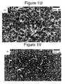
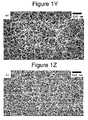
- FIGS. 1C-1Zare micrographs of nanofabrics grown with exemplary processes according to certain embodiments of the invention.
- FIG. 2is a cross-sectional view of an exemplary structure used to practice certain embodiments of the invention.
- FIG. 3Ashows a structure, according to certain embodiments of the invention, having a distribution of nanoparticles that may be used in an exemplary method of growing nanofabric.
- FIGS. 3B-Cillustrate exemplary methods of growing nanotube fabric by CVD using the structure of FIG. 3A .
- FIGS. 3D-3Fare micrographs of nanofabrics grown with exemplary processes according to certain embodiments of the invention.
- FIGS. 3G-Hillustrate exemplary methods of growing nanotube fabric by CVD using the structure of FIG. 3A .
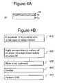
- FIG. 4Ashows a structure, according to certain embodiments of the invention, having a thin layer of metal catalyst and having a distribution of nanoparticles that may be used in an exemplary method of growing nanofabric.
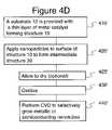
- FIGS. 4B-Dillustrate exemplary methods of growing nanotube fabric by CVD using the structure of FIG. 4A .
- FIG. 5Ashows a structure, according to certain embodiments of the invention, in which a nanofabric is formed over a substrate.
- FIG. 5Billustrates an exemplary method of forming nanotube fabric by spin-coating preformed nanotubes in suspension.
- FIGS. 5C-5Hare micrographs of nanofabrics formed with exemplary processes according to certain embodiments of the invention.
- FIGS. 5I-Jillustrate exemplary methods of forming nanotube fabric by spin-coating preformed nanotubes in suspension.
- FIG. 6are cross-sectional views of exemplary structures according to certain embodiments of the invention.
- FIG. 7shows cross-sectional views of exemplary structures according to certain embodiments of the invention.
- FIG. 8Ashows cross-sectional views of exemplary structures according to certain embodiments of the invention.
- FIGS. 8B-Dare micrographs of nanofabrics patterned according to certain embodiments of the invention.
- Preferred embodiments of the inventionprovide nanotube films, layers, or non-woven fabrics and methods of making same so that they form, or may be made to form, various useful patterned components, elements or articles.
- filmsfilms
- layerslayers
- non-woven fabricsare referred to as “fabrics” or “nanofabrics”.
- the components created from the nanofabricsretain desirable physical properties of the nanotubes and/or the nanofabrics from which they are formed.
- preferred embodimentsallow modern manufacturing techniques (e.g., those used in semiconductor manufacture) to be readily employed to utilize the nanofabric articles and devices.
- the nanofabricsmay be patterned into ribbons, which can be used to create non-volatile electromechanical memory cells.
- the ribbonsmay be used as a component of a non-volatile electromechanical memory cell.
- the deflected, physical state of the ribbonmay be made to represent a corresponding information state.
- the deflected, physical statehas non-volatile properties, meaning the ribbon retains its physical (and therefore informational) state even if power to the memory cell is removed.
- the nanofabricmay also be formed into conductive traces or pads. As explained in U.S. patent application Ser. Nos.
- the tracehas advantageous electrical and thermal conductivity, allowing it to be used for extremely small feature sizes, or to be utilized as a transistor component, such as a gate or base of a transistor forming superior metal to semiconductor contacts.
- the nanofabricsmay also be formed or patterned into shorter segments such as ribbons or patches. The shorter segments or patches allow facile interconnection of their nanotubes to vias, interconnects, traces or other structures useful in electronic devices. They may also be used to create new forms of electromechanical memory cells, for example, non-crossbar, embedded cells.
- the articles so formedhelp enable the generation of nanoelectronic devices and may also be used to assist in increasing the efficiency and performance of current electronic devices using a hybrid approach (e.g., using nanoribbon memory cells in conjunction with semiconductor addressing and processing circuitry).
- Preferred nanofabricshave a plurality of nanotubes in contact so as to form a non-woven fabric. Gaps in the fabric, i.e., between nanotubes either laterally or vertically, may exist.
- the fabricpreferably has a sufficient amount of nanotubes in contact so that at least one electrically conductive, semi-conductive or mixed conductive and semi-conductive pathway exists from a given point within a ribbon or article to another point within the ribbon or article (even after patterning of the nanofabric).
- nanofabricsmay also be used.
- nanofabricsthat are primarily a monolayer with sporadic bilayers and trilayers, but other embodiments benefit from thicker fabrics with multiple layers.
- the technique chosenmust result in a sufficient quantity of nanotubes in contact with other nanotubes which thereby matte as a result of the nanotubes' adhesion characteristics.
- Certain embodimentse.g., memory cells
- SWNTssingle-walled nanotubes
- Other embodimentse.g., conductive traces
- the nanotubeshave a resistance per square between 1-1000 k ⁇ / ⁇ (a lower resistance per square value is generally preferred) but can be tuned to have a resistance per square between 1 k ⁇ / ⁇ -10 M ⁇ / ⁇ which is dependent upon the quality of nanotubes used and their electrical and mechanical characteristics.
- the porosity of the fabriccan be tuned as well to generate low density fabrics with high porosity and high density fabrics with low porosity.
- the average length of a nanotuberanges between 50-1000 nm and 1-100 ⁇ m including single-walled nanotubes, multi-walled nanotubes or a mixture of both and can be controlled as is necessary for a particular application such as memory, switches, relays, chemical sensors, biosensors and resonators.
- Certain preferred methods of constructing the nanofabricsinvolve growing nanotubes using chemical vapor deposition (CVD) processes in conjunction with various catalysts. Other preferred methods generate films using spin-coating techniques with preformed nanotubes.
- the fabricsmay be patterned after being formed or they may be grown or formed in a predetermined pattern, e.g., by using patterned catalyst metal layers, nanoparticles or a combination thereof.
- Carbon nanotubescan be grown on substrates whose surfaces contain certain metallic or oxide layers.
- the metallic or metal oxide layersallow metal-containing nanoparticles to be applied onto the substrate surface.
- Exemplary nanoparticlesinclude metals, such as iron, cobalt, nickel, tungsten, molybdenum, rhenium and other transition metals, or metal oxides.
- the metals or metal oxides in these methodsact as growth catalyst for carbon nanotubes.
- SWNTssingle-walled nanotubes
- catalyst solutionse.g., “liquid catalysts” (see Cassell, A., et al., Journal of Physical Chemistry B, 103, 6484, 1999 and Cassell, A., et al., Journal Am. Chem. Soc., 121, 7975, 1999), and layered catalytic deposition (see Cassell, A., et al., Journal of Physical Chemistry B, 103, 6484, 1999).
- Metal oxides of various diametersmay be used depending upon whether growth of single-walled nanotubes (SWNTs) or multi-walled nanotubes is desired. (See, e.g., Y. Li, W.
- Bi-metallic catalyst nanoparticles(iron-molybdenum) have also been fabricated to assist in the production of carbon nanotubes (see Li, Y. and Liu, J., Chem. Mater., 13, 1008, 2001). These nanoparticles are usually dispersed randomly on a substrate or other support to produce nanotube growth.
- Typical liquid catalystscontain a mixture of chlorides or nitrates that have iron, cobalt, nickel, or molybdenum.
- These liquid catalystsare generated by soaking a pre-patterned ‘stamp’ onto a substrate. After stamping, the catalyst is calcinated or oxidized to burn off all the chlorides, nitrides, and other species leaving a random distribution of metal nanoparticles within a broad size regime.
- Yet another method of producing SWNTsinvolves the deposition of metal layers (see Delzeit, L., et al., Chemical Physics Letters, 348, 368, 2001).
- the metal layersmay include a porous under-layer such as aluminum or iridium, a catalytic layer (iron, cobalt, nickel), and a co-catalyst layer, typically molybdenum.
- the catalyst nanoparticles required for nanotube formationare produced during the CVD process.
- the inventorshave discovered that the above techniques may be extended to create nanofabrics, which have important characteristics that may be controlled in the creation process.
- theyhave discovered new techniques to create nanofabrics.
- the fabricscan be assembled or grown (e.g., over an entire wafer surface) and then fabric may be selectively removed, e.g., by using lithographic patterning.
- the fabricmay be formed in a pattern; i.e., nanotube fabric will grow in places where desired and none need be removed subsequent to growth.
- the metallic nanoparticlesmay be applied to the substrate surface in a variety of ways, including spin coating, application via aerosol, or by dipping the substrate into a solution that includes such nanoparticles.
- the metallic nanoparticles used as catalystmay also be applied to the substrate surface by deposition of a gas-phase metallic precursor such as any metallocene including ferrocene, molybdocene, cobaltocene and many other derivatives known in the literature to vaporize at relatively low temperatures, e.g. 25-600° C. (i.e., a low temperature relative to the temperatures at which carbon nanotube growth would occur using that metal as catalyst).
- a gas-phase metallic precursorsuch as any metallocene including ferrocene, molybdocene, cobaltocene and many other derivatives known in the literature to vaporize at relatively low temperatures, e.g. 25-600° C. (i.e., a low temperature relative to the temperatures at which carbon nanotube growth would occur using that metal as catalyst).
- an appropriate feedstock gasis supplied to the substrate's environment using a CVD process and nanotubes are allowed to grow. Typical growth times range from under 1 minute to 60 minutes. A typical growth phase can be completed in less than ten minutes.
- appropriate feedstock gassesinclude, but are not limited to CO, CH 4 , C 2 H 4 and other carbon sources.
- the feedstock gasshould be used at proper flow rates and at proper concentrations with inert gasses such as argon or nitrogen. Typical temperature regimes are about 600-1000° C.
- Some factors influencing nanotube growthinclude catalyst composition, catalyst diameter, catalytic growth efficiency, temperature, CVD run time and choice of reagents including catalysts and feedstock gasses as well as reductants and inert carrier gasses, flow rates, ratios of gasses and mixtures and substrate type and composition.
- the films generated by this methodare typically characterized in bulk by resistance in ohms per square ( ⁇ / ⁇ ) measurements that range from 1 to 1000 k ⁇ / ⁇ or in some circumstances from 1 to 20 M ⁇ / ⁇ . This measurement can be used to describe the quality and density of the tubes in bulk growth where lower resistance per square indicates a denser fabric and a relatively high concentration of metallic nanotubes.
- One preferred method of growing nanofabricsuses CVD techniques with substrates having a thin layer of metal catalyst on the substrate surface.
- the thin layersallow the catalyst to be easily removed in subsequent processing steps. Thicker catalyst layers may require more difficult processing steps.
- FIG. 1Ashows a cross-sectional view of an exemplary structure 10 having a substrate 12 and a thin metal catalyst layer 14 (shown here as one layer, though more than one layer may be employed). This figure is not to scale; the metal catalyst layer of typical embodiments is only about 1-2 nm thick.
- An exemplary, non-limiting substrate 12is made of silicon and has an upper layer of SiO 2 (not shown).
- the SiO 2insulates the conductive nanotubes (once formed) from the underlying bulk silicon of substrate 12 .
- the upper layer of the substrate 12may already have formed therein various elements that may be used together with the to-be-formed nanofabric articles to form circuits and the like, or the articles may be used as conductive connections between circuits formed on the substrate.
- the metals that can be used as primary catalyst metals of layer 14can be selected from a non-exclusive group known to produce SWNTs, such as iron, nickel, cobalt, and molybdenum.
- Metal layer 14can also include metals that act in conjunction with primary catalysts as co-catalysts, such metals include, but are not limited to, aluminum, molybdenum, cobalt, or other co-catalyst metals. If multi-walled nanotubes (MWNTs) are desired, these and additional transition metals may be used in layer 14 , such as yttrium, lanthanides and actinides.
- the growth of nanotubes from deposited thin metal layers 14typically involves the deposition by any physical vapor deposition technique of an aluminum layer, an iron layer, and/or a molybdenum layer, onto a substrate 12 .
- the aluminum layergenerates a porous reactive support that aids in generation of carbon species which feed into the iron catalyst where growth of the nanotubes actually takes place.
- the molybdenum layeralso serves as a site to reduce the carbon to a reactive form. The iron by itself can accomplish this reduction even but in some cases the rate is increased if the Mo and Al are present as well.
- the thin metal layers 14such as aluminum and molybdenum assist in the formation of SWNTs during CVD (when these three metals are used in concert, iron is the primary growth catalyst).
- These layersare extremely thin (e.g., 1-2 nm) and will diffuse or vaporize during CVD growth. Some of the particles created from such vaporization may be encapsulated by the eventually-grown nanotubes. (As the nanotubes are growing, the thin layers will diffuse. When layers are heated, they have a tendency to generate particles. Some of these particles will contain iron which will then be the site of the direct growth of carbon nanotubes. If in some instances the catalyst is very small, then the catalyst particle will be carried along as the nanotube grows. In other cases the catalyst particle will be larger and the nanotube will grow out from this end leaving the catalyst particle in place. Either way, if one looks at a transmission electron micrograph of a nanotube, one will almost always find at one end a nanoparticle, which acted as a catalyst.)
- FIG. 1B.1illustrates a way of forming nanofabrics utilizing a substrate with thin metal catalyst layer(s).
- an intermediate structure 10is provided 110 .
- the structureas outlined above, includes a substrate 12 and a metal catalyst layer 14 .
- a furnaceis heated 120 to about 500° C.
- the structure 10is placed 130 into the furnace.
- the metal layer 12may be oxidized 140 in air.
- the oxidationcan take place at 500° C. for 30 minutes. Oxidizing may be desired because it generates nanoparticles on the surface when metal atoms migrate and rearrange themselves.
- the temperature of the substrate 10is ramped up to the CVD temperature and a flow of feedstock and inert gasses is provided 150 .
- hydrogen gasis mixed with an inert gas that has proper heat diffusion properties (typically argon or nitrogen).
- the ratio of the gassescan be 1:5 hydrogen to inert gas (the ratio, however, should depend on the flow rate and types of gas introduced into the system upon reaching CVD temperature). For example, methane at a flow rate of 100-750 standard cubic centimeters per minute (sccm), or ethylene gas at 1.0-5.0 sccm may be used.
- the CVD runis performed 160 for some time typically between 1-10 minutes.
- a CVD process or chemical vapor depositioninvolves in this case a carrier gas (argon), a reductant (hydrogen) and a carbon feedstock (methane, ethylene in combination or alone, or other gas)).
- the furnaceis ramped down 170 to less than 200° C. in a flow of inert gas or gasses that have low or no reactivity with the carbon sources, such as argon or nitrogen.
- the gas usedcould be air or oxygen at a lower temperature; such use would provide a final annealing 180 for nanotube adhesion and/or removal of amorphous carbon.
- a nanofabricis created over substrate 12 and the thin metal layer 14 is substantially or totally vaporized.
- the surface of the substrate 12may have a defined pattern (e.g., a grating) on its surface.
- the surfacemay have alternating regions of metal or semiconductor and insulator.
- the metal or semiconducting embedded materialsmay be partially or totally capped off by a sacrificial layer which can be removed later to provide a suspended nanotube nanoribbon structure. See U.S. patent application Ser. Nos. 09/915,093 and 10/033,323.
- a defined thin metal layer patternwill determine the origination of nanotube growth. (That is, nanotube growth will originate from the catalyst regions rather than the interstitial regions which do not have catalyst. This characteristic may be exploited; i.e., depending on the ultimate use of the nanoribbons or nanofabric articles, a specific surface pattern may be desired (for example in a memory device).
- the thin metal layer catalystmay be patterned to create a patterned growth of nanofabric. If the catalyst patterns are sufficiently far away from each other they may not require subsequent patterning.
- FIG. 2is a cross-sectional view of an exemplary structure 15 having a grating configuration.
- Surface metal regions 17are separated from one another by insulating regions 19 .
- the material of metal regions 17may be selected from appropriate carbon nanotube growth catalysts, and the insulating regions 19 may be made from material that does not readily initiate carbon nanotube growth and genesis, such as silica.
- the separate metal catalyst layer regions 17provide a region where nanotube growth originates.
- the density of the nanotube ribbonmay be controlled by altering such variables as catalyst composition and concentration, growth environment, including but not limited to growth time (e.g., less CVD run time yields less dense nanofabric), temperature, gas composition and concentration.
- growth timee.g., less CVD run time yields less dense nanofabric
- temperaturee.g., less carbonate
- gas compositione.g., hydrogen
- Thin metal layers of aluminum, iron, and molybdenum(15 nm, 1 nm, and 2 nm, respectively) are sequentially deposited on a substrate.
- the substrateis placed in a tube furnace in which the temperature is ramped to 500° C. and held for thirty minutes, in an ambience of air.
- the temperatureis then ramped to a CVD temperature of 850° C. in a flow of argon gas and hydrogen gas, at 100:400 sccm Ar:H 2
- methane gas at a flow rate of 500 sccmis introduced into the furnace for a 1 minute growth time.
- the furnaceis ramped down to below 200° C. in an argon atmosphere.
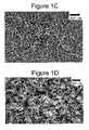
- FIG. 1Cis a micrograph of a fabric made from this procedure.
- FIG. 1Dis a micrograph of the nanotube growth resulting from such use of ethylene.
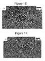
- Examples 3-6show that the rate of methane gas flow affects the production of nanotube fabrics in typical CVD methods. From the micrographs one can see how the change in gas flow from 725 to 500 to 250 sccm affects the amount of growth. These examples show that the porosity and type of nanotubes grown may be controlled by changing specific parameters in the growth process. The growth of nanotubes is sustained over this range and can be finely controlled to generate primarily multilayer fabrics (750 sccm) to primarily monolayer fabrics (250 sccm). Reduction in gas flow to even lower levels is possible to assure primarily monolayer fabrics. An increase of the concentration would allow growth of fabrics with multilayers. Other parameters such as growth time and temperature can be controlled in concert with feedstock gas flow to provide more control over the fabric's characteristics.
- Example 3Methane is flowed at 725 sccm and the argon and hydrogen gas flow are kept constant at 100 sccm and 400 sccm, respectively.
- CVDis performed as above with the following parameters: the CVD is performed at 850° C. for 1 minute with the following metal layers: 15 nm aluminum, 1 nm iron and 2 nm molybdenum.
- FIG. 1Eis a micrograph of the film which resulted from this procedure.
- Example 4All parameters are kept the same as example 3 except methane gas flow is 500 sccm.
- FIG. 1Fis a micrograph of the film which resulted from this procedure.
- Example 5All parameters are kept the same as example 3 except methane gas flow is 250 sccm.
- FIG. 1Gis a micrograph of the film which resulted from this procedure.
- Example 6All parameters are kept the same as example 3 except methane gas flow is 100 sccm.
- FIG. 1His a micrograph of the film which resulted from this procedure.
- Examples 7-9mirror examples 3-6 in that the flow rates of ethylene gas used are decreased in sequential CVD processes, while keeping all other variables constant. As above, all of these examples show fine control may be achieved over the growth density, nanotube porosity, nanotube length and the resistance per square values. (Resistance per square is used to assess in general the porosity of the nanotubes and/or their overall conductive quality.) Figures for examples 7-9, respectively, show fabrics corresponding to decreasing the gas flow. As flow decreases, the fabric density decreases and resistance increases.
- Example 7The argon flow and hydrogen flow are kept constant at 100 sccm and 400 sccm, respectively. Ethylene gas is flowed at 5.0 sccm. Metal layers are as follow: 5.0 nm aluminum, 1.0 nm iron and 2.0 nm molybdenum, the CVD temperature is 800° C., and is run for 10 minutes.
- FIG. 1Iis a micrograph of the film, which resulted from this procedure.
- Example 8All parameters are kept the same as example 7 except ethylene gas flow is 2.5 sccm.
- FIG. 1Jis a micrograph of the film which resulted from this procedure.
- Example 9All parameters are kept the same as example 7 except ethylene gas flow is 1.0 sccm.
- FIG. 1Kis a micrograph of the film which resulted from this procedure.
- Examples 10-12show the effects of reducing CVD temperatures while keeping all other parameters constant.
- the CVD methodsare otherwise much the same as in example 1. These examples also show that fine control may be achieved in porosity, thickness and length of nanofabrics and nanotubes.
- Figures for examples 10-12, respectively,show fabrics corresponding to decreasing CVD temperatures. As the temperature decreases, the fabric density decreases, and the resistance increases.
- Example 10CVD is performed on a substrate of silicon coated with 15 nm aluminum, 1 nm iron and 2 nm molybdenum, using a 725 sccm flow of methane gas at 900° C. for ten minutes in Ar/H flow as above.
- FIG. 1Lis a micrograph of the film which resulted from this procedure.
- Example 11All parameters are kept the same as in example 10, except the CVD temperature is decreased to 850° C.
- FIG. 1Mis a micrograph of the film which resulted from this procedure.
- Example 12All parameters are kept the same as in example 10, except the CVD temperature is decreased to 800° C.
- FIG. 1Nis a micrograph of the film which resulted from this procedure.
- Figures for examples 13-16, respectively,show fabrics corresponding to decreasing CVD run time. As the run time decreases, the fabric density decreases, and the resistance increases.
- Example 13CVD is run for 10 minutes on a substrate of silicon coated with 15 nm aluminum, 1 nm iron, and 2 nm molybdenum at 850° C. in a 725 sccm flow of methane gas and 100:400 sccm Ar:H 2 as above.
- FIG. 1Ois a micrograph of the film which resulted from this procedure.
- Example 14All parameters are kept the same as example 13, except the CVD run time is decreased to five minutes.
- FIG. 1Pis a micrograph of the film which resulted from this procedure.
- Example 15All parameters are kept the same as in example 13, except the CVD run time is decreased to two minutes.
- FIG. 1Qis a micrograph of the film which resulted from this procedure.
- Example 16All parameters are kept the same as in example 13, except the CVD run time is decreased to one minute.
- FIG. 1Ris a micrograph of the film which resulted from this procedure.
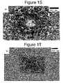
- Examples 17-20show the effect that varying the thicknesses of the aluminum metal layer has on the resulting films. As above, all of these examples show fine control may be achieved over the growth density, nanotube porosity, nanotube length and the resistance per square values. Figures for examples 17-20, respectively, show fabrics corresponding to decreasing thickness of the metal layer catalyst. As the thickness decreases, the fabric density decreases, and the resistance increases.
- Example 17CVD is performed on a substrate of silicon coated with 25 nm aluminum, 1 nm iron and 2 nm molybdenum, using a 725 sccm flow of methane gas and the argon and hydrogen gas flow are kept constant at 100 sccm and 400 sccm, respectively, at 850° C. for ten minutes.
- FIG. 1Sis a micrograph of the film which resulted from this procedure.
- Example 18All parameters are kept the same as in example 17, except the thickness of the aluminum layer is decreased to 15 nm.
- FIG. 1Tis a micrograph of the film which resulted from this procedure.
- Example 19All parameters are kept the same as in example 17, except the thickness of the aluminum layer is decreased to 5 nm.
- FIG. 1Uis a micrograph of the film which resulted from this procedure.
- Example 20All parameters are kept the same as in example 17, except the thickness of the aluminum layer is decreased to 0 nm (no aluminum is deposited in this example).
- FIG. 1Vis a micrograph of the film which resulted from this procedure.
- Examples 21-22show the results of altering thin metal layer thickness and using silicon dioxide as substrate. Altering the metal layer thickness allows tuning of the porosity and specifically the type of nanotubes. Thicker layers are more conducive to growing MWNTs while thinner layers grow better SWNTs and leave less residual metal because they are vaporized at the high temperatures of nanotube growth.
- Figures for examples 21-22, respectively,show fabrics corresponding to decreasing thickness of the metal layer catalyst. As the thickness decreases, the fabric density decreases, and the resistance increases.
- Example 21CVD is performed on a silicon dioxide substrate coated with thin metal layers; 2.0 nm aluminum, 0.5 nm iron and 1.0 nm molybdenum at 850° C. in a 500 sccm flow of methane gas in 100:400 sccm Ar:H 2 for one minute.
- FIG. 1Wis a micrograph of the film which resulted from this procedure.
- Example 22All parameters are kept the same as example 21, except thin metal layers of the following thicknesses; 1.0 nm aluminum, 0.5 nm iron and 1.0 nm molybdenum were used.
- FIG. 1Xis a micrograph of the film which resulted from this procedure.
- Examples 23 and 24show the films that are grown by CVD on silicon and silicon dioxide substrates. These examples illustrate control over porosity even on different substrates.
- a semiconducting substrate and an insulating substrateare examples of a semiconducting substrate and an insulating substrate. Growth is achievable on a variety of substrate layers allowing ready integration into typical semiconductor process flows and ease of manufacture.
- Figures for example 23 and 24show that the fabric density changes with the type of substrate, and thus resistance changes.
- Example 23CVD is performed on a silicon substrate coated with thin metal layers; 15 nm aluminum, 1.0 nm iron and 2.0 nm molybdenum at 850° C. in a 500 sccm flow of methane gas for two minutes.
- FIG. 1Yis a micrograph of the film which resulted from this procedure.
- Example 24All parameters are kept the same as example 23, except silicon dioxide is used as substrate.
- FIG. 1Zis a micrograph of the film which resulted from this procedure.
- Another preferred method of growing nanofabricsuses metallic or metal oxide nanoparticles (e.g., iron oxide) as carbon nanotube growth catalyst.
- Metallic or metal-oxide nanoparticleshave a narrow range of diameters. This narrow range can lead to more effective control over the diameter and type of nanotubes forming the eventual nanofabric.
- the surface of the substrate usedcan be derivitized to create a more hydrophobic or hydrophilic environment to promote better adhesion of the catalyst particles.
- the nature of the substrateallows control over the level of dispersion of the nanoparticles to a precision sufficient to generate monolayer nanotube fabrics.
- FIG. 3Ashows a cross-sectional view of an exemplary structure 20 used to grow nanofabrics.
- a substrate 12has a distribution 16 of metallic or metal oxide nanoparticles thereon.
- the substrate surface used for generation of carbon nanotubesmay be any material including, but not limited to, silicon, thermal oxide, silicon oxide, silicon nitride, tungsten, tungsten/titanium and other typical insulators, semiconductors and metallic surfaces commonly used in CMOS and semiconductor fabrication processes the surface may have electronic components and patterns already defined therein, as mentioned above, and the substrate may be functionalized or non-functionalized.
- FIG. 3Billustrates a way of growing a nanofabric using a substrate coated with nanoparticles 16 .
- a mixture of ferritin and wateris created.
- ferritin dissolved in deionized (DI) water at a typical concentration (1-1000 ⁇ M) (SIGMA catalog)is provided.
- DIdeionized
- the ferritincontains naturally encapsulated iron in an organic layer or shell, and can be processed so that the encapsulated iron may be used in subsequent nanotube generation.
- This shellis oxidized using air or oxygen oxidation or plasma ashing, which causes its removal leaving only an iron oxide nanoparticle.
- the iron oxide nanoparticlesare reduced to leave metallic iron nanoparticles which catalyze the growth of nanotubes.
- the purpose of using ferritin or any appropriate nanoparticlesis to cause the nanoparticles to be dispersed on the surface in an even fashion (monodisperse). Ferritin particles have a very narrow diameter range as do the nanoparticles
- the ferritin solutionis applied 310 to a surface of substrate 12 .
- the substrateBefore application the substrate can be derivitized to make it more hydrophilic or hydrophobic in order to promote adhesion of the ferritin to the surface.
- the substrateis allowed to dry 320 (e.g. approximately five minutes has been found to be sufficient). This leaves a coating of ferritin on the surface of the substrate.
- the protein shellsare then removed 330 from the ferritin particles.
- the structuremay be subjected to either an oxidation operation at 400-800° C. for about 15 minutes, or it may be subjected to a plasma ashing operation.
- the oxidation processremoves substantially all of the proteinaceous shell from the ferritin, thereby leaving behind a coating 16 of nanoparticles of iron oxide.
- the nanoparticlesare approximately two to five nanometers in diameter, or more particularly approximately three nanometers in diameter. See Li, 46 Journal Physical Chem. above.)
- CVDmay be performed 340 to grow a nanofabric of nanotubes.
- the nanofabricmay be grown, for example, over an entire wafer surface as a monolayer of contacting nanotubes.
- the above embodimentis conducive to growing a conductive (primarily) monolayer fabric with sufficient density to remain suspended over a switching junction.
- metal ligand-catalyst precursor moleculesare used to deposit metallic nanoparticles on a functionalized substrate surface to thereby help create growth of nanotubes.
- the formula of the metal/ligand complexwill have a formula such as ML, in which M is a metal such as iron, cobalt, or nickel, and L is one or more organic ligands having an affinity for the metal.
- Mis a metal such as iron, cobalt, or nickel
- Lis one or more organic ligands having an affinity for the metal.
- One general formulamay be C x H y (COOH), but other carbon, oxygen, nitrogen and/or sulfur-containing ligands are known and may be used.
- a metallic nanoparticle ligated to an organic moietyis deposited on a functionalized substrate surface.
- the surfaceis functionalized to optimize ligand bonding during spin coating, a procedure which may result in minimal deposition of untreated nanoparticles.
- Certain embodimentsuse a generic method to synthesize metallic nanoparticles with organic shells which have a very specific size regime for example 3-5 nm which can be monodisperse on a substrate.
- Iron oxide nanoparticlesare applied to a substrate in a concentration sufficient to support the desired density of nanotube growth.
- the substrateis then subjected to a CVD operation as described herein.
- the substrateoptionally, can be dried and/or oxidized prior to beginning the CVD run.
- iron oxide nanoparticlesmay be applied to a substrate surface by spin coating.
- iron oxideis suspended in deionized water at a 1:10 ratio.
- the aqueous iron suspensionis applied to a substrate surface, and the surface is spun at approximately 1000 rpm to distribute the suspension.
- the surfaceis then spun at 4000 rpm to dry the suspension.
- More than one application of iron oxide nanoparticlesmay be performed. The number of applications of iron oxide nanoparticles required will vary depending on the concentration of the suspension used, the desired resulting surface density of nanoparticles, the physical properties of the desired fabric, and the physical properties of the substrate used.
- FIG. 3Cillustrates a way of growing a nanofabric using liquid metal catalyst.
- a liquid metal catalystis created.
- a dissolved metal catalyste.g., iron nitrate (Fe(NO 3 ) 3
- Fe(NO 3 ) 3is mixed with methanol and applied onto a substrate 350 .
- the substrateis oxidized 360 , e.g., by ashing, thereby leaving a dispersion of iron oxide nanoparticles on the surface of the substrate.
- the substrateis then subjected to a CVD operation 370 to grow nanotubes.
- CVD operation 370Provided below are several exemplary ways of growing nanofabrics using the above principles.
- HMDShexamethyldisilane
- Iron nanoparticlesare made by dissolving Fe(NO 3 ) 3 in solution of a lauric acid in methanol at a ratio of 1:3.3 Fe:lauric acid.
- the nitrate solutionis evacuated to pump off nitric acid, and the solvent.
- the dried iron nanoparticlesare then added to 10 mL toluene and 10 mL isopropanol to resuspend the nanoparticles in solution.
- the Fe nanoparticle solutionis then diluted 1:25 in isopropanol.
- FIG. 3Dis a micrograph of a nanofabric which resulted from this procedure.
- nanoparticles in this embodimentcan be tuned to a particular size by changing the organic ligand (analogous to the protein shell of ferritin) that is bound to the metal. Additionally, nanoparticles of different metal or metal oxide species may be mixed together in a solution and applied for use as catalyst, e.g., 50% Fe and 50% Co, or 33% Fe 33% Co and 33% Al, or any other appropriate combinations.
- FIG. 3Eis a micrograph of a nanofabric which resulted from this procedure.
- Example 27demonstrates the growth of carbon nanotubes from a substrate with ferritin on the surface.
- the processinvolves the use of ferritin as a catalyst precursor.
- a 1:10 mixture of ferritin in deionized wateris applied to a silica surface of a wafer.
- the waferis dried, leaving a dispersed coating of ferritin on the surface of the substrate.
- the substrateis oxidized to remove all non-iron, organic matter and placed in the oven.
- the ovenis ramped to 700° C. for 10 minutes in Ar:H 2 , then it is ramped to 800° C. for seven minutes in Ar:H 2 .
- CVDis performed at 800° C. with a 10 sccm flow of ethylene for 40 minutes in 600:400 sccm Ar:H 2 .
- FIG. 3Fshows a FESEM micrograph of carbon nanotubes grown using ferritin as catalyst precursor.
- Another preferred method of growing nanofabricsuses nanoparticles in conjunction with thin metal layers on a substrate surface. This method allows one to easily distribute catalyst particles while taking advantage of the ease of thin layer deposition and their properties in assisting the process of growing nanotubes. Recall that aluminum and molybdenum are useful in generating surface carbon precursors that grow nanotubes.
- FIG. 4Ashows a cross-sectional view of an exemplary structure 30 used to grow nanofabrics.
- a substrate 12has a thin layer 14 of metal catalyst and a distribution 16 of nanoparticles thereover.
- the substrate surface used for generation of carbon nanotubesmay be any material including, but not limited to silicon or thermal oxide, e.g. silicon oxide, alumina.
- the uppermost layercan be an insulator, semiconductor or metal.
- Typical substrates which are of interestinclude silicon dioxide (SiO 2 ), silicon nitride (Si 3 N 4 ), titanium, titanium/tungsten and others used in standard CMOS and semiconductor processing.
- the surfacemay have already formed therein various components and structures (e.g., gratings) of the aforementioned materials. In addition, the surface may be functionalized or non-functionalized.
- FIG. 4Billustrates a way of growing a nanofabric of carbon nanotubes (e.g., to cover a wafer surface) by using nanoparticles in conjunction with thin metal layers.
- a substrate 12is provided and a thin layer of metal catalyst is provided 410 to at least selected regions of a wafer or perhaps an entire wafer surface, as described above. This forms layer 14 of metal catalyst.
- a distribution of nanoparticles 16is applied 420 to the surface of layer 14 . This may be done using any of the above methods of applying nanoparticles, e.g., spin coating suspensions of nanoparticles.
- Catalyst precursorssuch as ferritin, liquid metal catalyst precursor and metal ligand-catalyst precursor molecules may also be used in conjunction with thin metal layers on substrates to grow carbon nanotube fabrics.
- the substratemay be dried (optionally) 425 .
- the substrateis oxidized 430 .
- the structure 30may be subjected to a CVD process 440 to form a nanofabric.
- Nanotubesshould be sufficiently free of amorphous carbon if the nanotubes are to be used as electronic elements.
- this techniqueis more conducive to semiconductor manufacturing environments than growth of nanotubes by CVD because it uses a room temperature process that does not contribute to the thermal budget of the standard CMOS process flows or semiconductor manufacturing methods. Additionally, the overall cost of this integration of nanotubes is very inexpensive.
- FIG. 5Ashows an exemplary structure 50 having a wafer substrate 12 and a nanofabric 54 thereover.
- the nanofabric 54may be made to cover an entire wafer surface.
- the substratemay be any material that will accept the deposition of nanotubes by spin coating, but preferably a material chosen from the group consisting of a thermal oxide or nitride, including but not limited to silicon dioxide, silicon nitride, alumina on silicon, or any combination of the following on silicon or silicon dioxide: aluminum, molybdenum, iron, titanium, platinum, and aluminum oxide, or any other substrate useful in the semiconductor industry.
- a thermal oxide or nitrideincluding but not limited to silicon dioxide, silicon nitride, alumina on silicon, or any combination of the following on silicon or silicon dioxide: aluminum, molybdenum, iron, titanium, platinum, and aluminum oxide, or any other substrate useful in the semiconductor industry.
- FIG. 5Bshows a way of making a fabric of nanotubes on a functionalized carbon nanotube growth substrate surface 52 .
- the substrate surface 52may be prepared for spin coating by functionalizing the surface.
- functionalization of a wafer/substrate surfaceinvolves derivitizing the surface of the substrate. For example, one could chemically convert a hydrophilic to hydrophobic state or provide functional groups such as amines, carboxylic acids, thiols or sulphonates to alter the surface characteristics of the substrate.
- Functionalizationmay include the optional primary step 510 of oxidizing or ashing the substrate in oxygen plasma to remove carbon and other impurities from the substrate surface and to provide a uniformly reactive, oxidized surface which is then reacted with a silane.
- the substrate surface 52may be derivitized 520 prior to application of a nanotube suspension to enhance bonding of the nanotubes.
- APTS3-aminopropyltriethoxysilane
- the substrate surface 52may be derivitized 520 prior to application of a nanotube suspension to enhance bonding of the nanotubes.
- any reactive silanecould be used in functionalization of such a surface.
- the substrate surface 52is exposed to an approximately 1 to 50 millimolar solution of APTS in suitable organic solvent, e.g. hexane, but more preferably 13 to 28 millimolar APTS in hexane, such that approximately a monolayer of APTS is deposited on the substrate surface.
- the substrateIn order to form such a monolayer of APTS, the substrate typically is immersed in an APTS solution for 30 minutes. Once the surface 52 is prepared for spin coating, carbon nanotubes are dispered 530 on the surface, and the surface is subjected to spinning in order to disperse the nanotubes, forming a nanotube fabric (e.g., fabric 54 of FIG. 5A ). The substrate is then (optionally) annealed 540 .
- a nanotube fabrice.g., fabric 54 of FIG. 5A
- Nanotubesmay be employed to apply nanotubes to surfaces to form nanofabrics: to attain desired fabric properties; the selection of one method over another depends, in part, on the properties of the pre-formed nanotubes being used. For example, under certain embodiments laser-ablated SWNTs are used; under other embodiments, commercially-available high pressure carbon monoxide decomposition SWNTs nanotubes are used, such as HiPcoTM nanotubes available from Rice University; under still other embodiments, other nanotubes may be used.
- laser-ablated nanotubesare mixed with a solvent at a concentration of about 100-500 ⁇ g/mL.
- Solvents which are quite useful for suspension of SWNTs and distribution via spin coatinginclude isopropanol, methanol, ethanol, 1,2 dichlorobenzene, 1,3 dichlorobenzene, 1,4 dichlorobenzene, chlorobenzene, n-methylpyrollidinone, dimethylformamide, dimethylsulfoxide, acetonitrile, hexane, toluene, methylene chloride and chloroform. While all of these solvents have the ability to suspend nanotubes, the precise characteristics of the film desired and substrate used are important for solvent selection. If a low boiling solvent is desired hexane would, for example, be a better selection than DMSO. 1,2 dichlorobenzene is a preferred solvent owing to its excellent suspension properties and compatibility with industrial semiconductor processes.
- HiPcoTM nanotubesmay be used.
- the HiPcoTM nanotubesare SWNTs and relatively free from amorphous deposits, fibrous deposits and other impurities.
- HiPcoTM tubesare mixed into orthodichlorobenzene at a more dilute concentration than are laser ablated nanotubes, typically 10-200 ⁇ g/mL.
- the preferred concentrationdepends on the length of the nanotubes used. Laser ablated nanotubes tend to have overall greater lengths than HiPcoTM tubes. Regardless of the nanotubes used, the nanotubes in mixture should be adequately dispersed, e.g., by sonication.
- Adequately-dispersed nanotubesmay be applied 530 onto a substrate surface by spin coating. Such a surface should be relatively free of any residue remaining after storage or after any substrate preparation step, e.g. functionalization of the surface. If solvent, e.g. hexane is present on the substrate's surface, it may be removed, e.g., by baking at 100-115° C. for 1 minute. After removal of any storage solvent, the nanotubes are spun onto the substrate surface.
- solvente.g. hexane
- One way of spin coating the nanotubesinvolves spinning the substrate, for example, at 1000 rpm while depositing the nanotube solution on the substrate surface, for about 30 seconds or alternatively they can be applied before the spinning has begun.
- the substratemay (i.e., optionally) then be dried, for example, by spinning at 4000 rpm until dry.
- Further coats of nanotube suspensionmay be applied in like manner, until the substrate surface is coated with the desired density of nanotubes. Ribbon density may be varied based on desired use.
- Adequate layers of nanotubestypically have resistance per square measurements between 1-1000 k ⁇ / ⁇ . For particular applications, nanotube layers with resistances per square below 1 k ⁇ / ⁇ may be preferred, and for yet other uses, nanotube films with resistance per square measurements of 1-10 M ⁇ / ⁇ may be sufficient.
- the substrate surfacetypically has a redundancy of electrically conductive pathways.
- a layer of nanotubes of desired densityi.e., a monolayer
- the substratemay be baked 540 once again to remove any remaining solvent, e.g., at 100-115° C.
- a fabric resistance per square of ⁇ 100 k ⁇is typically measured. The actual resistance per square depends upon the quality of the nanotubes used, their compositions, and overall purity.
- a non-functionalized substrate surfacemay be coated with nanotubes by spin coating.
- the surfacemay be oxidized, e.g., by ashing in oxygen plasma, to remove surface impurities, or it may be coated and not oxidized.
- the nanotubes usedmay be, but are not limited to, laser-ablated SWNTs or HiPcoTM nanotubes.
- Adequately dispersed nanotubesmay be deposited on a non-functionalized substrate surface by spin coating.
- the substratemay be spun at 1000 rpm for 30 seconds while applying a nanotube solution to the substrate surface to distribute the nanotubes or the solution may be applied first and then spun. Further coats of nanotube suspension may be applied until the substrate surface is coated with the desired density of nanotubes.
- the substratemay be dried (optionally) between application steps, e.g., by spinning at 4000 rpm until dry.
- ribbon densitymay be varied based on desired use.
- eight coatings of the nanotube suspensionare applied to the non-functionalized substrate surface, when using the preceding parameters, to attain a fabric of electrically conductive nanotubes.
- the substratecan be baked once again to remove any remaining solvent, e.g. at 100-115° C.
- Such a methodtypically results in a nanotube layer resistance per square measurement of ⁇ 1-100 k ⁇ which is dependent both on the number of applications performed and the purity and character of the nanotubes used.
- nanotubes that have been deposited on a surfacemay be solvated and removed by subsequent applications of nanotubes in solvent, it may be desirable to cure the substrate and nanotubes before subsequent applications of solvated nanotubes. Such curing may be accomplished through evaporation or drying.
- Another way of limiting the subsequent dissolution and removal of already-spun-on tubesis to use a different solvent for subsequent spin coating steps.
- the density of the nanotube ribbonmay be controlled by altering such variables as including but not limited to functionalization of the underlying surface, spin coating parameters (length of time and RPM), solvent choice, nanotube type and concentration, diameter and length of nanotubes, number of applications and substrate type and composition.
- a wafer substrateis first ashed in oxygen plasma for 15 minutes. After ashing, the substrate is bathed for 30 minutes in a solution of 3-aminopropyltriethoxysilane (APTS), the functionalization agent, and hexane at a ratio of 30-60 ⁇ L of APTS to 10 mL of Hexane.
- APTS3-aminopropyltriethoxysilane
- hexaneat a ratio of 30-60 ⁇ L of APTS to 10 mL of Hexane.
- APTS3-aminopropyltriethoxysilane
- hexaneat a ratio of 30-60 ⁇ L of APTS to 10 mL of Hexane.
- a nanotube solutionis prepared.
- HiPcoTM SWNTsare mixed in a solution comprising 1 mg of nanotubes and 50 ml 1,2 dichlorobenzene.
- the nanotube solutionis then sonicated for 1 hour to
- the substrateBefore nanotube deposition, the substrate is removed from the hexane bath and is baked at 100-115° C. for 1 minute to remove any solvent residue. After baking, the nanotubes are spun onto the wafer at 1000 rpm for 30 seconds to distribute the nanotubes, and then they are spun at 4000 rpm to dry the wafer. Four such SWNT spin coatings are applied to the wafer. After spinning, the wafer is baked again at 100-115° C. to remove any remaining solvent.
- FIGS. 5C-Ddisplay FESEM images of different magnifications of HiPcoTM SWNTs spun onto a functionalized surface.
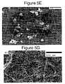
- FIG. 5Edisplays a FESEM image of spun-on laser-ablated SWNTs with a functionalized surface. Some particles containing amorphous carbon impurities are observed also.
- FIG. 5Fdisplays a micrograph of a nanofabric spun on to the substrate according to this method; the micrograph shows that nanotubes conform to a substrate surface via van der Waals attraction.
- conformal nanofabricsmay be useful in fabrication of non-horizontal electromechanical switches, especially vertical electromechanical switches or also as interconnects, actuators, relays, sensors and other electronic elements.
- Carbon nanotubesare deposited on a non-functionalized surface as follows. A wafer surface is ashed for 1 minute. A nanotube solution is deposited and spun on to the wafer as presented in Example 28, above. Eight applications of nanotube mixture are applied to the wafer surface, producing resistance per square measurements on varying sections of the nanotube fabric ranging from 50 to 100 k ⁇ .
- FIG. 5Gdisplays an FESEM image of SWNTs spun onto a non-functionalized wafer surface with sufficient applications to generate a multilayer nanofabric.
- FIG. 5Hdisplays an FESEM micrograph of a monolayer fabric spun onto a substrate which has a prefabricated metal electrode with a width of about 130 nm shown.
- Preferred embodimentsoperate with a range of concentrations for pre-formed nanotubes.
- concentrations for laser ablated nanotubesa concentration of about 0.1-0.5 mg/mL (100-500 ug/mL) is used.
- concentrationis preferably adjusted depending upon the purity and length of the nanotubes; for example, shorter nanotubes have one spinning regime and longer ones have a different regime.
- preferred embodimentspreferably subject the nanotube solution to sonication.
- preferred embodimentsuse sonication times such as 30-120 minutes.
- the new and improved methods for creating nanofabricsmay be used to create articles therefrom.
- the U.S. patent applications, identified and incorporated above,describe specific (but not limiting) uses of such fabrics and articles.
- the various masking and patterning techniques for selectively removing portions of the fabricare described in these applications but are not repeated here for the sake of brevity.
- various component architecturesare described in the incorporated applications but not repeated here for the sake of brevity.
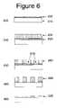
- FIG. 6is a cross-sectional view of exemplary structures used in creating patterned nanofabrics.
- This methodcreates patches of carbon nanotube fabric which can be used as electronic elements.
- Such a patch of nanotube fabricmay be used as an electromechanical switch, or as an electronic interconnect.
- An intermediate structure 600is provided.
- Structure 600comprises a nanofabric 620 overlying a substrate 610 .
- the substrate 610could be a simple substrate made of a single material; it could be a substrate which has already undergone some processing, e.g., to include vias, plugs or other elements, etc.
- the nanofabric 620may be grown or formed using any of the methods disclosed or incorporated above.
- the nanofabricmay be of SWNTs or multi-walled nanotubes.
- a layer of resist 630is applied over the nanofabric 620 to form intermediate structure 640 .
- the resist 630is then patterned using any of a variety of techniques, including but not limited to those described in the incorporated references.
- the resistmay be patterned to correspond to the desired pattern of nanofabric patches, so that the resist will cover (and define) the desired patches. Removing selected portions of the resist (e.g., exposed portions) will create intermediate structure 650 .
- the intermediate structure 650includes exposed nanofabric portions 670 and remaining resist portions 660 .
- the exposed nanofabric portions 670may be removed in many ways; for example, by performing a reactive ion etch procedure, or oxidizing the substrate, by plasma ashing, air oxidation or other reaction methods to remove all nanotube fabric except for the desired patches, thereby creating intermediate structure 680 .
- the remaining resist portions 660may then be stripped from intermediate structure 680 , yielding structure 690 which includes patterned patches 695 of nanofabric.
- the nanofabric 620may be formed or grown over defined regions of sacrificial material and over defined support regions.
- the sacrificial materialmay be subsequently removed, yielding suspended articles of nanofabric. See, for example, Electromechanical Memory Array Using Nanotube Ribbons and Method for Making Same (U.S. patent application Ser. No. 09/915,093) filed Jul. 25, 2001, for an architecture which suspends ribbons of nanofabric.
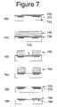
- FIG. 7is a cross-sectional view of exemplary structures used in creating suspended, patterned nanofabrics. This method creates suspended patches of carbon nanotube fabric, which can be used as electronic elements. Such a patch of nanotube fabric may be used as an electromechanical switch, or as an actuator, a relay, a sensor, especially a biosensor or chemical sensor.
- Structure 700comprises defined regions of sacrificial material 720 overlying a substrate 710 (which as outlined above could made of a single material; could be a substrate which has already undergone some processing, e.g. to include vias, plugs or other elements, etc.).
- a nanofabric 730covers the substrate surface and the sacrificial material 720 .
- the nanofabric 730may be formed or grown as outlined above and may be multilayer or single layer and may have single- or multi-walled nanotubes.
- a layer of resist 740is applied over the nanofabric 730 to create intermediate structure 745 . The resist 740 is then patterned (not shown).
- the intermediate structure 750includes exposed nanofabric portions 770 and remaining resist portions 760 .
- the exposed nanofabric portions 770may be removed in many ways; for example, by performing a reactive ion etch procedure, or oxidizing the substrate, by plasma ashing, air oxidation or other reactive methods to remove all nanotube fabric except for the desired patches, thereby creating intermediate structure 780 .
- the remaining resist portions 760may then be stripped from intermediate structure 780 , yielding structure 790 which includes patterned nanofabric patches 795 overlying defined sacrificial material 720 .
- the sacrificial layer 720is removed by selective etching, leaving substantially intact the suspended patterned nanofabric 795 and leaving an air gap 798 in the place of the removed sacrificial layer.
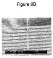
- FIG. 8Ais a cross-sectional view of exemplary structures used in creating suspended, patterned nanofabrics.
- This methodcreates suspended patches of carbon nanotube fabric overlying an electrode with which the nanofabric may come into electrically conductive contact when the nanofabric is deflected.
- Such a devicecan be used as an electronic element, e.g. as an electromechanical switch, etc.
- Structure 800comprises a substrate 810 (similar to those described above) with already defined electrodes 820 (e.g., made of sufficiently conductive material, such as doped semiconductor or metal) and defined sacrificial material 830 thereover.
- a nanofabric 840covers the substrate surface and the sacrificial layer 830 .
- the nanofabricmay be made by any of the above-described methods. Similar to that described above and as described in the incorporated references, the nanofabric 840 may be patterned (e.g., lithographic patterning) and defined portions of nanofabric may be removed to form intermediate structure 850 . Patterned nanofabric articles 860 then cover defined sacrificial material 830 which in turn cover electrodes 820 .
- Structure 870comprises suspended nanofabric articles 860 separated from electrodes 820 .
- the nanofabric articles 860 and/or the electrodesmay then be subjected to electrical stimulus to cause the nanofabric articles 860 to deflect toward, or away from, electrodes 820 .
- the deflected articlesretain their deflected state in a non-volatile manner.
- a wafer substrate, an overlying nanofabric, an embedded titanium electrode under a sacrificial layer of Al 2 O 3are provided.
- Shipley 1805 photoresistis applied to the wafer surface by spin coating at 4000 rpm for 60 seconds.
- the photoresistis exposed using a Kasper Mask Aligner for 8 seconds.
- the patternis developed using a basic developer, thereby exposing portions of nanofabric and leaving other portions protected by the photoresist.
- the substrateis rinsed in deionized water and dried at 115° C.
- the exposed portions of nanofabricare removed by plasma ashing for five minutes with 25 cubic feet per minute oxygen at a pressure of 280 millitorr and a power of 300 Watts.
- FIG. 8Bdisplays an FESEM image of patterned nanofabrics made by this method.
- bare substrate regionsare dark, nanofabric patches are light in color and the longitudinal light stripe is a metallic electrode.
- Typical resistivity for a patterned trace with a length of 100 ⁇ m and width of 3 ⁇ mis 1-10 M ⁇ .
- FIG. 8Cdisplays an FESM image of the same structure as in 8 B under greater magnification.
- the dark longitudinal stripeis the sacrificial layer overlying the metal electrode.
- FIG. 8Ddisplays an FESM image of the same structure with the sacrificial layer removed; the nanofabric can be seen suspended over and not in contact with the electrode.
- Other embodimentsinvolve controlled composition of carbon nanotube fabrics.
- methodsmay be employed to control the relative amount of metallic and semiconducting nanotubes in the nanofabric.
- the nanofabricmay be made to have a higher or lower percentage of metallic nanotubes relative to semiconducting nanotubes.
- other properties of the nanofabrice.g., resistance
- the controlmay be accomplished by direct growth, removal of undesired species, or application of purified nanotubes.
- nanotube fabricWith regard to application of purified nanotubes, using proper bulk nanotube preparations which contain primarily metallic or semiconducting nanotubes would allow application of a nanotube fabric to a substrate.
- the applicationcould be performed via spin coating of a nanotube stock solution onto a substrate, dipping a substrate into a nanotube stock solution, spraying of nanotube stock solutions onto a surface or other methods.
- Application of single-walled, multiwalled or mixtures of such nanotubescan be envisioned with subsequent patterning and etching to generate fabrics or traces of sufficient length and width to make electronic devices.
- FIG. 1B.2is similar to FIG. 1B.1 and the description thereof is not repeated.
- the method of FIG. 1B.2removes the optional step of annealing nanotubes found in FIG. 1B.1 and substitutes it with a selective removal of nanotubes, e.g., removing semiconducting nanotubes or metallic. By doing so the composition of the nanofabric may be controlled.
- FIGS. 3G-His similar to FIGS. 3B-C and the descriptions thereof are not repeated.
- the method of FIG. 3Gadds a selective removal 345 of nanotubes, e.g., removing semiconducting nanotubes or metallic; analogously, the method of FIG. 3H adds a selective removal 380 of nanotubes. By doing so the composition of the nanofabric may be controlled.
- FIG. 4Cis similar to FIG. 4B and the description thereof is not repeated.
- the method of FIG. 4Cadds a selective removal 450 of nanotubes, e.g., removing semiconducting nanotubes or metallic. By doing so the composition of the nanofabric may be controlled.
- FIG. 4Dis similar to FIG. 4B and the description thereof is not repeated.
- the method of FIG. 4Dsubstitutes the CVD step 440 of FIG. 4B with a selective growth 440 ′ of nanotubes, in which the growth process affects the relative concentration of one type of nanotube as compared to another. By doing so the composition of the nanofabric may be controlled.
- the application of nanotubesmay be iterative.
- a nanofabricmay be created and subsequently processed to remove semiconducting nanotubes and then another application of nanotubes may be applied. Repeated application and removal will increase the relative amount of metallic or semiconducting nanotubes in the resulting nanofabric.
- FIG. 5Iis similar to FIG. 5B and the description thereof is not repeated.
- the method of FIG. 5Iremoves the optional annealing step 540 of FIG. 5B and adds a selective removal 550 of nanotubes, e.g., removing semiconducting nanotubes or metallic. By doing so the composition of the nanofabric may be controlled. This process step 550 can be iterated to generate a more dense nanofabric.
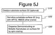
- FIG. 5Jis similar to FIG. 5B and the description thereof is not repeated.
- the method of FIG. 5Iremoves the optional annealing step 540 of FIG. 5B and substitutes the dispersal step 530 with a new dispersal step 530 ′, in which the nanotubes that are disperse have a controlled composition, e.g., selected amounts of metallic nanotubes. By doing so the composition of the nanofabric may be controlled.
- This process step 530 ′can be iterated to generate a more dense nanofabric.
- Catalyst deposited on substrate surface or remaining in spun-on SWNTsmay be removed by rinse/wash steps if a desired property of the ribbon included that it be free of metal/catalyst. This could be performed by successive treatments in an appropriate solvent or acid which would cause the removal of the exterior carbon shell that typically passivates the particles during nanotube growth. Other unreacted nanoparticles could be removed with just a mild solvent wash.
- nanofabrics and patterning articles therefromare conducive to certain environments, such as a circuit manufacturing environment.
- Other methodsprovide nanofabrics and articles therefrom that have desirable characteristics, such as an ability to adhere to hydrophobic surfaces (found in many electronic devices), even when the feature size is in the nanometer regime ( ⁇ 200 nm).
- the previous methodsillustrate that control over catalyst type, catalyst distribution, surface derivitization, temperature, feedstock gas types, feedstock gas pressures and volumes, reaction time and other conditions allow growth of fabrics of single-walled, multi-walled or mixed single- and multi-walled nanotube fabrics that are at the least monolayers in nature but could be thicker as desired with measurable electrical characteristics.
Landscapes
- Engineering & Computer Science (AREA)
- Chemical & Material Sciences (AREA)
- Nanotechnology (AREA)
- Materials Engineering (AREA)
- Crystallography & Structural Chemistry (AREA)
- Physics & Mathematics (AREA)
- Condensed Matter Physics & Semiconductors (AREA)
- General Physics & Mathematics (AREA)
- Organic Chemistry (AREA)
- Composite Materials (AREA)
- Inorganic Chemistry (AREA)
- Chemical Kinetics & Catalysis (AREA)
- Manufacturing & Machinery (AREA)
- Mathematical Physics (AREA)
- Theoretical Computer Science (AREA)
- Carbon And Carbon Compounds (AREA)
Abstract
Description
Claims (29)
Priority Applications (13)
| Application Number | Priority Date | Filing Date | Title |
|---|---|---|---|
| US10/341,005US7566478B2 (en) | 2001-07-25 | 2003-01-13 | Methods of making carbon nanotube films, layers, fabrics, ribbons, elements and articles |
| TW092101535ATWI307330B (en) | 2001-07-25 | 2003-01-24 | Methods of making non-woven fabric of carbon nanotubes and article |
| US10/776,572US6924538B2 (en) | 2001-07-25 | 2004-02-11 | Devices having vertically-disposed nanofabric articles and methods of making the same |
| US10/776,059US7259410B2 (en) | 2001-07-25 | 2004-02-11 | Devices having horizontally-disposed nanofabric articles and methods of making the same |
| US11/158,217US7112464B2 (en) | 2001-07-25 | 2005-06-21 | Devices having vertically-disposed nanofabric articles and methods of making the same |
| US11/158,544US7274078B2 (en) | 2001-07-25 | 2005-06-22 | Devices having vertically-disposed nanofabric articles and methods of making the same |
| US11/193,795US7304357B2 (en) | 2001-07-25 | 2005-07-29 | Devices having horizontally-disposed nanofabric articles and methods of making the same |
| US11/526,364US7719067B2 (en) | 2001-07-25 | 2006-09-25 | Devices having vertically-disposed nanofabric articles and methods of making the same |
| US11/999,228US7619291B2 (en) | 2001-07-25 | 2007-12-04 | Devices having horizontally-disposed nanofabric articles and methods of making the same |
| US12/510,579US20090283745A1 (en) | 2001-07-25 | 2009-07-28 | Methods of making carbon nanotube films, layers, fabrics, ribbons, elements and articles |
| US12/945,501US9574290B2 (en) | 2003-01-13 | 2010-11-12 | Methods for arranging nanotube elements within nanotube fabrics and films |
| US13/076,152US9422651B2 (en) | 2003-01-13 | 2011-03-30 | Methods for arranging nanoscopic elements within networks, fabrics, and films |
| US15/241,495US10124367B2 (en) | 2003-01-13 | 2016-08-19 | Methods for arranging nanoscopic elements within networks, fabrics and films |
Applications Claiming Priority (3)
| Application Number | Priority Date | Filing Date | Title |
|---|---|---|---|
| US09/915,093US6919592B2 (en) | 2001-07-25 | 2001-07-25 | Electromechanical memory array using nanotube ribbons and method for making same |
| US10/128,118US6706402B2 (en) | 2001-07-25 | 2002-04-23 | Nanotube films and articles |
| US10/341,005US7566478B2 (en) | 2001-07-25 | 2003-01-13 | Methods of making carbon nanotube films, layers, fabrics, ribbons, elements and articles |
Related Parent Applications (4)
| Application Number | Title | Priority Date | Filing Date |
|---|---|---|---|
| US09/915,093Continuation-In-PartUS6919592B2 (en) | 2001-07-25 | 2001-07-25 | Electromechanical memory array using nanotube ribbons and method for making same |
| US10/033,323Continuation-In-PartUS6911682B2 (en) | 2001-07-25 | 2001-12-28 | Electromechanical three-trace junction devices |
| US10/128,118Continuation-In-PartUS6706402B2 (en) | 2001-07-25 | 2002-04-23 | Nanotube films and articles |
| US10128118Continuation-In-Part | 2003-01-13 |
Related Child Applications (7)
| Application Number | Title | Priority Date | Filing Date |
|---|---|---|---|
| US10/128,118Continuation-In-PartUS6706402B2 (en) | 2001-07-25 | 2002-04-23 | Nanotube films and articles |
| US10/776,059Continuation-In-PartUS7259410B2 (en) | 2001-07-25 | 2004-02-11 | Devices having horizontally-disposed nanofabric articles and methods of making the same |
| US10/776,572Continuation-In-PartUS6924538B2 (en) | 2001-07-25 | 2004-02-11 | Devices having vertically-disposed nanofabric articles and methods of making the same |
| US11/158,217Continuation-In-PartUS7112464B2 (en) | 2001-07-25 | 2005-06-21 | Devices having vertically-disposed nanofabric articles and methods of making the same |
| US11/158,544Continuation-In-PartUS7274078B2 (en) | 2001-07-25 | 2005-06-22 | Devices having vertically-disposed nanofabric articles and methods of making the same |
| US11/193,795Continuation-In-PartUS7304357B2 (en) | 2001-07-25 | 2005-07-29 | Devices having horizontally-disposed nanofabric articles and methods of making the same |
| US12/510,579ContinuationUS20090283745A1 (en) | 2001-07-25 | 2009-07-28 | Methods of making carbon nanotube films, layers, fabrics, ribbons, elements and articles |
Publications (2)
| Publication Number | Publication Date |
|---|---|
| US20080299307A1 US20080299307A1 (en) | 2008-12-04 |
| US7566478B2true US7566478B2 (en) | 2009-07-28 |
Family
ID=40088572
Family Applications (2)
| Application Number | Title | Priority Date | Filing Date |
|---|---|---|---|
| US10/341,005Expired - LifetimeUS7566478B2 (en) | 2001-07-25 | 2003-01-13 | Methods of making carbon nanotube films, layers, fabrics, ribbons, elements and articles |
| US12/510,579AbandonedUS20090283745A1 (en) | 2001-07-25 | 2009-07-28 | Methods of making carbon nanotube films, layers, fabrics, ribbons, elements and articles |
Family Applications After (1)
| Application Number | Title | Priority Date | Filing Date |
|---|---|---|---|
| US12/510,579AbandonedUS20090283745A1 (en) | 2001-07-25 | 2009-07-28 | Methods of making carbon nanotube films, layers, fabrics, ribbons, elements and articles |
Country Status (1)
| Country | Link |
|---|---|
| US (2) | US7566478B2 (en) |
Cited By (52)
| Publication number | Priority date | Publication date | Assignee | Title |
|---|---|---|---|---|
| US20060237805A1 (en)* | 2003-05-14 | 2006-10-26 | Nantero, Inc. | Sensor platform using a horizontally oriented nanotube element |
| US20080090082A1 (en)* | 2006-10-11 | 2008-04-17 | Samsung Electro-Mechanics Co., Ltd. | Methods for surface modification of non-dispersible metal nanoparticles and modified metal nanoparticles for inkjet by the same method |
| US20080142850A1 (en)* | 2005-05-09 | 2008-06-19 | Nantero, Inc. | Memory elements and cross point switches and arrays of same using nonvolatile nanotube blocks |
| US20080157127A1 (en)* | 2005-05-09 | 2008-07-03 | Nantero, Inc. | Nonvolatile nanotube diodes and nonvolatile nanotube blocks and systems using same and methods of making same |
| US20080157126A1 (en)* | 2005-05-09 | 2008-07-03 | Nantero, Inc. | Nonvolatile nanotube diodes and nonvolatile nanotube blocks and systems using same and methods of making same |
| US20080157257A1 (en)* | 2005-05-09 | 2008-07-03 | Nantero, Inc. | Nonvolatile nanotube diodes and nonvolatile nanotube blocks and systems using same and methods of making same |
| US20080170429A1 (en)* | 2005-05-09 | 2008-07-17 | Nantero, Inc. | Nonvolatile nanotube diodes and nonvolatile nanotube blocks and systems using same and methods of making same |
| US20080212361A1 (en)* | 2005-05-09 | 2008-09-04 | Nantero, Inc. | Nonvolatile nanotube diodes and nonvolatile nanotube blocks and systems using same and methods of making same |
| US20080238882A1 (en)* | 2007-02-21 | 2008-10-02 | Ramesh Sivarajan | Symmetric touch screen system with carbon nanotube-based transparent conductive electrode pairs |
| US20080251723A1 (en)* | 2007-03-12 | 2008-10-16 | Ward Jonathan W | Electromagnetic and Thermal Sensors Using Carbon Nanotubes and Methods of Making Same |
| US20090087630A1 (en)* | 2001-07-25 | 2009-04-02 | Nantero, Inc. | Carbon nanotube films, layers, fabrics, ribbons, elements and articles |
| US20090140167A1 (en)* | 2005-09-06 | 2009-06-04 | Natero, Inc. | Nanotube fabric-based sensor systems and methods of making same |
| US20090211460A1 (en)* | 2007-11-20 | 2009-08-27 | Kwok Kuen So | Bowl and basket assembly and salad spinner incorporating such an assembly |
| US20100001267A1 (en)* | 2008-06-20 | 2010-01-07 | Nantero, Inc. | Nram arrays with nanotube blocks, nanotube traces, and nanotube planes and methods of making same |
| US20100050866A1 (en)* | 2006-09-27 | 2010-03-04 | Electronics and Telecommunications Research Instiitute | Nanowire filter, method for manufacturing the same, method for removing material absorbed thereon, and filtering apparatus having the same |
| US20100051880A1 (en)* | 2004-12-16 | 2010-03-04 | Ghenciu Eliodor G | Aqueous carbon nanotube applicator liquids and methods for producing applicator liquids thereof |
| US20100072957A1 (en)* | 2004-06-18 | 2010-03-25 | Bertin Claude L | Nanotube-based logic driver circuits |
| US20100147657A1 (en)* | 2004-11-02 | 2010-06-17 | Nantero, Inc. | Nanotube esd protective devices and corresponding nonvolatile and volatile nanotube switches |
| US20100148183A1 (en)* | 2001-07-25 | 2010-06-17 | Ward Jonathan W | Method of Forming a Carbon Nanotube-Based Contact to Semiconductor |
| US20100267205A1 (en)* | 2005-09-06 | 2010-10-21 | Lockheed Martin Corporation | Carbon nanotubes for the selective transfer of heat from electronics |
| US7858185B2 (en) | 2003-09-08 | 2010-12-28 | Nantero, Inc. | High purity nanotube fabrics and films |
| US20100327247A1 (en)* | 2005-09-06 | 2010-12-30 | Nantero, Inc. | Method and system of using nanotube fabrics as joule heating elements for memories and other applications |
| US20110027497A1 (en)* | 2009-07-31 | 2011-02-03 | Nantero, Inc. | Anisotropic nanotube fabric layers and films and methods of forming same |
| US20110034008A1 (en)* | 2009-08-07 | 2011-02-10 | Nantero, Inc. | Method for forming a textured surface on a semiconductor substrate using a nanofabric layer |
| US7915637B2 (en) | 2008-11-19 | 2011-03-29 | Nantero, Inc. | Switching materials comprising mixed nanoscopic particles and carbon nanotubes and method of making and using the same |
| US7915122B2 (en) | 2005-06-08 | 2011-03-29 | Nantero, Inc. | Self-aligned cell integration scheme |
| US20110083319A1 (en)* | 2004-11-02 | 2011-04-14 | Nantero, Inc. | Methods of making nanotube switches |
| US20110096587A1 (en)* | 2009-10-23 | 2011-04-28 | Nantero, Inc. | Dynamic sense current supply circuit and associated method for reading and characterizing a resistive memory array |
| US7948082B2 (en) | 2003-09-08 | 2011-05-24 | Nantero, Inc. | Method of fabricating a patterned nanoscopic article |
| US20110156009A1 (en)* | 2009-12-31 | 2011-06-30 | Manning H Montgomery | Compact electrical switching devices with nanotube elements, and methods of making same |
| US8125824B1 (en) | 2010-09-02 | 2012-02-28 | Lockheed Martin Corporation | Nanotube random access memory (NRAM) and transistor integration |
| US8147722B2 (en) | 2003-09-08 | 2012-04-03 | Nantero Inc. | Spin-coatable liquid for formation of high purity nanotube films |
| US8183665B2 (en) | 2005-11-15 | 2012-05-22 | Nantero Inc. | Nonvolatile nanotube diodes and nonvolatile nanotube blocks and systems using same and methods of making same |
| US8253171B1 (en) | 2009-08-27 | 2012-08-28 | Lockheed Martin Corporation | Two terminal nanotube switch, memory array incorporating the same and method of making |
| US8350360B1 (en) | 2009-08-28 | 2013-01-08 | Lockheed Martin Corporation | Four-terminal carbon nanotube capacitors |
| US8405189B1 (en) | 2010-02-08 | 2013-03-26 | Lockheed Martin Corporation | Carbon nanotube (CNT) capacitors and devices integrated with CNT capacitors |
| KR101284775B1 (en)* | 2011-09-30 | 2013-07-17 | 한국화학연구원 | Carbon nanotube network transistor element having high on/off ratio and manufacturing method thereof |
| US8562937B2 (en) | 2005-12-19 | 2013-10-22 | Nantero Inc. | Production of carbon nanotubes |
| US8574673B2 (en) | 2009-07-31 | 2013-11-05 | Nantero Inc. | Anisotropic nanotube fabric layers and films and methods of forming same |
| US8937575B2 (en) | 2009-07-31 | 2015-01-20 | Nantero Inc. | Microstrip antenna elements and arrays comprising a shaped nanotube fabric layer and integrated two terminal nanotube select devices |
| US8941094B2 (en) | 2010-09-02 | 2015-01-27 | Nantero Inc. | Methods for adjusting the conductivity range of a nanotube fabric layer |
| US9390790B2 (en) | 2005-04-05 | 2016-07-12 | Nantero Inc. | Carbon based nonvolatile cross point memory incorporating carbon based diode select devices and MOSFET select devices for memory and logic applications |
| US9422651B2 (en) | 2003-01-13 | 2016-08-23 | Nantero Inc. | Methods for arranging nanoscopic elements within networks, fabrics, and films |
| US9574290B2 (en) | 2003-01-13 | 2017-02-21 | Nantero Inc. | Methods for arranging nanotube elements within nanotube fabrics and films |
| US9650732B2 (en) | 2013-05-01 | 2017-05-16 | Nantero Inc. | Low defect nanotube application solutions and fabrics and methods for making same |
| US9666272B2 (en) | 2009-08-06 | 2017-05-30 | Nantero Inc. | Resistive change element arrays using resistive reference elements |
| US9911743B2 (en) | 2005-05-09 | 2018-03-06 | Nantero, Inc. | Nonvolatile nanotube diodes and nonvolatile nanotube blocks and systems using same and methods of making same |
| US10654718B2 (en) | 2013-09-20 | 2020-05-19 | Nantero, Inc. | Scalable nanotube fabrics and methods for making same |
| US10813257B2 (en)* | 2016-09-05 | 2020-10-20 | Nec Corporation | Electromagnetic wave absorbing material |
| US10920085B2 (en) | 2016-01-20 | 2021-02-16 | Honda Motor Co., Ltd. | Alteration of carbon fiber surface properties via growing of carbon nanotubes |
| US20230335307A1 (en)* | 2020-09-14 | 2023-10-19 | Nexans | Process for manufacturing a carbon-metal composite material and use thereof for manufacturing an electric cable |
| US12134820B2 (en)* | 2019-09-23 | 2024-11-05 | Agc Glass Europe | Process for making a fabric based substrate bearing a carbon based coating |
Families Citing this family (19)
| Publication number | Priority date | Publication date | Assignee | Title |
|---|---|---|---|---|
| US7329931B2 (en) | 2004-06-18 | 2008-02-12 | Nantero, Inc. | Receiver circuit using nanotube-based switches and transistors |
| US7713577B2 (en)* | 2005-03-01 | 2010-05-11 | Los Alamos National Security, Llc | Preparation of graphitic articles |
| US9287356B2 (en) | 2005-05-09 | 2016-03-15 | Nantero Inc. | Nonvolatile nanotube diodes and nonvolatile nanotube blocks and systems using same and methods of making same |
| KR100674404B1 (en)* | 2005-07-05 | 2007-01-29 | 재단법인서울대학교산학협력재단 | Carbon nanotube coated heat sink and its manufacturing method |
| JP4678687B2 (en)* | 2006-02-24 | 2011-04-27 | 公立大学法人大阪府立大学 | Method and apparatus for producing carbon nanostructure |
| US8115187B2 (en)* | 2007-05-22 | 2012-02-14 | Nantero, Inc. | Triodes using nanofabric articles and methods of making the same |
| US8723407B2 (en)* | 2008-02-12 | 2014-05-13 | The State Of Oregon Acting By And Through The State Board Of Higher Education On Behalf Of The University Of Oregon | Method of making zinc oxide nanowires |
| CN101754584B (en)* | 2008-12-12 | 2012-01-25 | 清华大学 | Method for preparing conducting lines |
| FR2943850B1 (en)* | 2009-03-27 | 2011-06-10 | Commissariat Energie Atomique | METHOD FOR MAKING ELECTRICAL INTERCONNECTIONS WITH CARBON NANOTUBES |
| WO2011035157A2 (en)* | 2009-09-18 | 2011-03-24 | Applied Materials, Inc. | Apparatus and methods for forming energy storage and photovoltaic devices in a linear system |
| GB2478269A (en)* | 2009-12-18 | 2011-09-07 | Surrey Nanosystems Ltd | Nanomaterials growth system and method |
| US20110203632A1 (en)* | 2010-02-22 | 2011-08-25 | Rahul Sen | Photovoltaic devices using semiconducting nanotube layers |
| US9362390B2 (en) | 2010-02-22 | 2016-06-07 | Nantero, Inc. | Logic elements comprising carbon nanotube field effect transistor (CNTFET) devices and methods of making same |
| US20110227043A1 (en) | 2010-03-19 | 2011-09-22 | International Business Machines Corporation | Graphene sensor |
| WO2011135824A1 (en)* | 2010-04-27 | 2011-11-03 | パナソニック株式会社 | Apparatus for producing metal oxide nanofibers and method for producing metal oxide nanofibers |
| US9634251B2 (en) | 2012-02-27 | 2017-04-25 | Nantero Inc. | Nanotube solution treated with molecular additive, nanotube film having enhanced adhesion property, and methods for forming the nanotube solution and the nanotube film |
| JP5808468B1 (en) | 2014-09-01 | 2015-11-10 | ニッタ株式会社 | Catalyst particle holding structure for producing carbon nanotube and method for producing the same |
| US10743400B2 (en)* | 2017-10-06 | 2020-08-11 | General Electric Company | Electron stripper foils and particle accelerators having the same |
| US11501812B2 (en)* | 2020-07-31 | 2022-11-15 | Taiwan Semiconductor Manufacturing Co., Ltd. | Semiconductor devices including ferroelectric memory and methods of forming the same |
Citations (304)
| Publication number | Priority date | Publication date | Assignee | Title |
|---|---|---|---|---|
| US3448302A (en) | 1966-06-16 | 1969-06-03 | Itt | Operating circuit for phase change memory devices |
| US3740494A (en) | 1970-11-24 | 1973-06-19 | Sescosem Soc Europ Semiconduct | Electromechanical vibration pick-ups and record pick-ups with field effect transistors |
| US3892890A (en) | 1972-05-12 | 1975-07-01 | Hitachi Ltd | Process for forming carbon coatings |
| US3970887A (en) | 1974-06-19 | 1976-07-20 | Micro-Bit Corporation | Micro-structure field emission electron source |
| US4324814A (en) | 1981-03-19 | 1982-04-13 | Rca Corporation | Method for forming a narrow thin film line |
| US4378629A (en) | 1979-08-10 | 1983-04-05 | Massachusetts Institute Of Technology | Semiconductor embedded layer technology including permeable base transistor, fabrication method |
| US4495511A (en) | 1982-08-23 | 1985-01-22 | The United States Of America As Represented By The Secretary Of The Navy | Permeable base transistor structure |
| US4510016A (en) | 1982-12-09 | 1985-04-09 | Gte Laboratories | Method of fabricating submicron silicon structures such as permeable base transistors |
| US4524431A (en) | 1982-02-01 | 1985-06-18 | Texas Instruments Incorporated | High-speed nonvolatile memory array |
| EP0217023A2 (en) | 1985-10-04 | 1987-04-08 | International Business Machines Corporation | Pipelined instruction execution with fast branch instructions |
| US4673474A (en) | 1984-10-16 | 1987-06-16 | Matsushita Electric Industrial Co., Ltd. | Molecular controlled structure and method of producing the same |
| US4694427A (en) | 1984-09-21 | 1987-09-15 | Kabushiki Kaisha Toshiba | Programmable semiconductor memory device with combined sense amplification and programming capability |
| US4707197A (en) | 1984-08-02 | 1987-11-17 | American Telephone And Telegraph Company, At&T Bell Laboratories | Method of producing a silicide/Si heteroepitaxial structure, and articles produced by the method |
| EP0269225A2 (en) | 1986-11-26 | 1988-06-01 | Energy Conversion Devices, Inc. | Thin film electrical devices with amorphous carbon electrodes and method of making same |
| US4758534A (en) | 1985-11-13 | 1988-07-19 | Bell Communications Research, Inc. | Process for producing porous refractory metal layers embedded in semiconductor devices |
| US4819212A (en) | 1986-05-31 | 1989-04-04 | Kabushiki Kaisha Toshiba | Nonvolatile semiconductor memory device with readout test circuitry |
| EP0315392A2 (en) | 1987-11-05 | 1989-05-10 | Energy Conversion Devices, Inc. | Data storage device having an encapsulated phase change memory medium and means for suppressing ablation thereof |
| US4853893A (en) | 1987-07-02 | 1989-08-01 | Ramtron Corporation | Data storage device and method of using a ferroelectric capacitance divider |
| US4876667A (en) | 1987-06-22 | 1989-10-24 | Energy Conversion Devices, Inc. | Data storage device having a phase change memory medium reversible by direct overwrite |
| US4888630A (en) | 1988-03-21 | 1989-12-19 | Texas Instruments Incorporated | Floating-gate transistor with a non-linear intergate dielectric |
| US4901121A (en) | 1985-03-29 | 1990-02-13 | American Telephone & Telegraph Co., At&T Bell Labs. | Semiconductor device comprising a perforated metal silicide layer |
| US4903090A (en) | 1984-11-19 | 1990-02-20 | Fujitsu Limited | Semiconductor device |
| US4939556A (en) | 1986-07-10 | 1990-07-03 | Canon Kabushiki Kaisha | Conductor device |
| EP0296716A3 (en) | 1987-06-22 | 1990-07-04 | Energy Conversion Devices, Inc. | Data storage device having a phase change memory medium reversible by direct overwrite and method of direct overwrite |
| US4947226A (en) | 1987-12-08 | 1990-08-07 | Hoenywell, Inc. | Bilateral switching device |
| US4979149A (en) | 1986-09-10 | 1990-12-18 | Lgz Landis & Gyr Zug Ag | Non-volatile memory device including a micro-mechanical storage element |
| US4985871A (en) | 1989-11-13 | 1991-01-15 | Chips And Technologies, Inc. | Memory controller for using reserved dram addresses for expanded memory space |
| US5010037A (en) | 1988-10-14 | 1991-04-23 | California Institute Of Technology | Pinhole-free growth of epitaxial CoSi2 film on Si(111) |
| US5031145A (en) | 1989-03-29 | 1991-07-09 | Hughes Microelectronics Limited | Sense amplifier |
| US5032538A (en) | 1979-08-10 | 1991-07-16 | Massachusetts Institute Of Technology | Semiconductor embedded layer technology utilizing selective epitaxial growth methods |
| EP0441409A3 (en) | 1987-07-29 | 1991-08-28 | Kabushiki Kaisha Toshiba | Nonvolatile semiconductor memory device |
| US5051956A (en) | 1988-03-25 | 1991-09-24 | Hughes Microelectronics Limited | Memory cell having means for maintaining the gate and substrate at the same potential |
| US5057883A (en) | 1989-05-10 | 1991-10-15 | Mitsubishi Denki Kabushiki Kaisha | Permeable base transistor with gate fingers |
| US5089545A (en) | 1989-02-12 | 1992-02-18 | Biotech International, Inc. | Switching and memory elements from polyamino acids and the method of their assembly |
| US5155561A (en) | 1988-01-05 | 1992-10-13 | Massachusetts Institute Of Technology | Permeable base transistor having an electrode configuration for heat dissipation |
| US5161218A (en) | 1989-11-13 | 1992-11-03 | Chips And Technologies, Inc. | Memory controller for using reserved DRAM addresses for EMS |
| US5168070A (en) | 1990-02-07 | 1992-12-01 | Forschungszentrum Julich Gmbh | Electronic component, especially a permeable base transistor |
| US5175597A (en) | 1990-06-15 | 1992-12-29 | Thomson-Csf | Semiconductor component with schottky junction for microwave amplification and fast logic circuits |
| US5184320A (en) | 1988-02-12 | 1993-02-02 | Texas Instruments Incorporated | Cached random access memory device and system |
| US5196396A (en) | 1991-07-16 | 1993-03-23 | The President And Fellows Of Harvard College | Method of making a superconducting fullerene composition by reacting a fullerene with an alloy containing alkali metal |
| US5198390A (en) | 1992-01-16 | 1993-03-30 | Cornell Research Foundation, Inc. | RIE process for fabricating submicron, silicon electromechanical structures |
| US5198994A (en) | 1988-08-31 | 1993-03-30 | Kabushiki Kaisha Toshiba | Ferroelectric memory device |
| US5216631A (en) | 1990-11-02 | 1993-06-01 | Sliwa Jr John W | Microvibratory memory device |
| US5252835A (en) | 1992-07-17 | 1993-10-12 | President And Trustees Of Harvard College | Machining oxide thin-films with an atomic force microscope: pattern and object formation on the nanometer scale |
| US5290715A (en) | 1991-12-31 | 1994-03-01 | U.S. Philips Corporation | Method of making dielectrically isolated metal base transistors and permeable base transistors |
| EP0613130A1 (en) | 1993-02-26 | 1994-08-31 | Nec Corporation | Carbon material originating from graphite and method of producing same |
| US5346683A (en) | 1993-03-26 | 1994-09-13 | Gas Research Institute | Uncapped and thinned carbon nanotubes and process |
| WO1995002709A3 (en) | 1993-07-15 | 1995-04-06 | Harvard College | EXTENDED NITRIDE MATERIAL COMPRISING β-C3N¿4? |
| US5412785A (en) | 1990-04-09 | 1995-05-02 | Motorola, Inc. | Microprogrammed data processor which includes a microsequencer in which a next microaddress output of a microROM is connected to the or-plane of an entry PLA |
| US5424054A (en) | 1993-05-21 | 1995-06-13 | International Business Machines Corporation | Carbon fibers and method for their production |
| US5426070A (en) | 1993-05-26 | 1995-06-20 | Cornell Research Foundation, Inc. | Microstructures and high temperature isolation process for fabrication thereof |
| EP0665187A1 (en) | 1994-01-28 | 1995-08-02 | Director-General Of The Agency Of Industrial Science And Technology | Method and device for the production of carbon nanotubes |
| US5444421A (en) | 1994-02-10 | 1995-08-22 | Racom Systems, Inc. | Low power consumption oscillator using multiple transconductance amplifiers |
| US5444651A (en) | 1991-10-30 | 1995-08-22 | Sharp Kabushiki Kaisha | Non-volatile memory device |
| US5453970A (en) | 1993-07-13 | 1995-09-26 | Rust; Thomas F. | Molecular memory medium and molecular memory disk drive for storing information using a tunnelling probe |
| US5456986A (en) | 1993-06-30 | 1995-10-10 | Carnegie Mellon University | Magnetic metal or metal carbide nanoparticles and a process for forming same |
| US5475341A (en) | 1992-06-01 | 1995-12-12 | Yale University | Sub-nanoscale electronic systems and devices |
| US5479172A (en) | 1994-02-10 | 1995-12-26 | Racom Systems, Inc. | Power supply and power enable circuit for an RF/ID transponder |
| US5517194A (en) | 1994-02-10 | 1996-05-14 | Racom Systems, Inc. | Passive RF transponder and method |
| US5521602A (en) | 1994-02-10 | 1996-05-28 | Racom Systems, Inc. | Communications system utilizing FSK/PSK modulation techniques |
| US5533061A (en) | 1994-02-10 | 1996-07-02 | Racom Systems, Inc. | Method and apparatus for detecting an FSK encoded carrier signal |
| US5538916A (en) | 1993-04-28 | 1996-07-23 | Mitsubishi Denki Kabushiki Kaisha | Method of manufacturing semiconductor device isolation region |
| US5547748A (en) | 1994-01-14 | 1996-08-20 | Sri International | Carbon nanoencapsulates |
| US5553099A (en) | 1994-02-10 | 1996-09-03 | Racom Systems, Inc. | FSK detector for determining an increasing time period between adjacent pulses of an FSK modulated square wave pulse train |
| US5563424A (en) | 1994-03-24 | 1996-10-08 | Uniax Corporation | Polymer grid triodes |
| WO1996038410A1 (en) | 1995-06-02 | 1996-12-05 | Forskningscenter Risø | Novel physically functional materials |
| US5586286A (en) | 1993-03-22 | 1996-12-17 | Compaq Computer Corporation | Memory controller having flip-flops for synchronously generating DRAM address and control signals from a single chip |
| WO1996041043A1 (en) | 1995-06-07 | 1996-12-19 | President And Fellows Of Harvard College | Carbide nanomaterials |
| US5590078A (en) | 1994-10-07 | 1996-12-31 | Mukesh Chatter | Method of and apparatus for improved dynamic random access memory (DRAM) providing increased data bandwidth and addressing range for current DRAM devices and/or equivalent bandwidth and addressing range for smaller DRAM devices |
| US5592642A (en) | 1988-12-22 | 1997-01-07 | Framdrive | Ferroelectric storage device emulating a rotating disk drive unit in a computer system and having an optical and parallel data interface |
| US5592643A (en) | 1988-12-22 | 1997-01-07 | Framdrive | Ferroelectric storage device emulating a rotating disk drive unit in acomputer system and having a parallel data interface |
| US5592644A (en) | 1988-12-22 | 1997-01-07 | Framdrive | Ferroelectric storage device emulating a rotating disk drive unit in a computer system and having an optical data interface |
| US5608888A (en) | 1991-03-15 | 1997-03-04 | C-Cube Microsystems, Inc. | Method and apparatus for mapping data of a 2-dimensional space from a linearly addressed memory system |
| US5608246A (en) | 1994-02-10 | 1997-03-04 | Ramtron International Corporation | Integration of high value capacitor with ferroelectric memory |
| WO1997009272A1 (en) | 1995-09-08 | 1997-03-13 | William Marsh Rice University | Ropes of single-wall carbon nanotubes |
| US5623638A (en) | 1994-11-22 | 1997-04-22 | Advanced Micro Devices, Inc. | Memory control unit with programmable edge generator to minimize delay periods for critical DRAM timing parameters |
| US5626670A (en) | 1994-10-03 | 1997-05-06 | American Research Corporation Of Virginia | Method for producing low thermal budget ferroelectric thin films for integrated device structures using laser-crystallization of spin-on sol-gel films |
| US5640133A (en) | 1995-06-23 | 1997-06-17 | Cornell Research Foundation, Inc. | Capacitance based tunable micromechanical resonators |
| US5640343A (en) | 1996-03-18 | 1997-06-17 | International Business Machines Corporation | Magnetic memory array using magnetic tunnel junction devices in the memory cells |
| US5650958A (en) | 1996-03-18 | 1997-07-22 | International Business Machines Corporation | Magnetic tunnel junctions with controlled magnetic response |
| US5651126A (en) | 1992-06-26 | 1997-07-22 | Apple Computer, Inc. | Method and apparatus for reducing transitions on computer signal lines |
| WO1997031139A1 (en) | 1996-02-26 | 1997-08-28 | President And Fellows Of Harvard College | Metal oxide nanorods |
| EP0426282B1 (en) | 1989-10-31 | 1997-10-29 | STMicroelectronics, Inc. | Programmable logic device |
| WO1997043473A1 (en) | 1996-05-15 | 1997-11-20 | Hyperion Catalysis International, Inc. | High surface area nanofibers |
| US5699317A (en) | 1992-01-22 | 1997-12-16 | Ramtron International Corporation | Enhanced DRAM with all reads from on-chip cache and all writers to memory array |
| WO1997022971A9 (en) | 1996-12-12 | 1998-01-29 | A negative voltage switch architecture for a nonvolatile memory | |
| US5716708A (en) | 1995-01-17 | 1998-02-10 | Lagow; Richard J. | Acetylenic carbon allotrope |
| US5719073A (en) | 1993-02-04 | 1998-02-17 | Cornell Research Foundation, Inc. | Microstructures and single mask, single-crystal process for fabrication thereof |
| US5739057A (en) | 1995-11-06 | 1998-04-14 | Tiwari; Sandip | Method of making self-aligned dual gate MOSFET with an ultranarrow channel |
| US5747180A (en) | 1995-05-19 | 1998-05-05 | University Of Notre Dame Du Lac | Electrochemical synthesis of quasi-periodic quantum dot and nanostructure arrays |
| EP0758028A3 (en) | 1995-07-10 | 1998-05-06 | Research Development Corporation Of Japan | Process of producing graphite fiber |
| US5751156A (en) | 1995-06-07 | 1998-05-12 | Yale University | Mechanically controllable break transducer |
| US5753088A (en) | 1997-02-18 | 1998-05-19 | General Motors Corporation | Method for making carbon nanotubes |
| WO1998026871A1 (en) | 1996-12-18 | 1998-06-25 | Eidgenössische Technische Hochschule Zürich | Nanotubes, use and manufacture of same |
| US5781717A (en) | 1996-09-19 | 1998-07-14 | I-Cube, Inc. | Dynamic spare column replacement memory system |
| US5780101A (en) | 1995-02-17 | 1998-07-14 | Arizona Board Of Regents On Behalf Of The University Of Arizona | Method for producing encapsulated nanoparticles and carbon nanotubes using catalytic disproportionation of carbon monoxide |
| US5799209A (en) | 1995-12-29 | 1998-08-25 | Chatter; Mukesh | Multi-port internally cached DRAM system utilizing independent serial interfaces and buffers arbitratively connected under a dynamic configuration |
| US5802583A (en) | 1996-10-30 | 1998-09-01 | Ramtron International Corporation | Sysyem and method providing selective write protection for individual blocks of memory in a non-volatile memory device |
| WO1998039251A1 (en) | 1997-03-07 | 1998-09-11 | President And Fellows Of Harvard College | Preparation of carbide nanorods |
| WO1998039250A1 (en) | 1997-03-07 | 1998-09-11 | William Marsh Rice University | Carbon fibers formed from single-wall carbon nanotubes |
| WO1998042620A1 (en) | 1997-03-21 | 1998-10-01 | Japan Fine Ceramics Center | Process for producing carbon nanotubes, process for producing carbon nanotube film, and structure provided with carbon nanotube film |
| WO1998048456A1 (en) | 1997-04-24 | 1998-10-29 | Massachusetts Institute Of Technology | Nanowire arrays |
| US5838165A (en) | 1996-08-21 | 1998-11-17 | Chatter; Mukesh | High performance self modifying on-the-fly alterable logic FPGA, architecture and method |
| US5847565A (en) | 1997-03-31 | 1998-12-08 | Council Of Scientific And Industrial Research | Logic device |
| US5850089A (en) | 1992-03-13 | 1998-12-15 | American Research Corporation Of Virginia | Modulated-structure of PZT/PT ferroelectric thin films for non-volatile random access memories |
| US5850231A (en) | 1993-04-13 | 1998-12-15 | Casio Computer Co., Ltd. | Electronic device having ferroelectric memory |
| US5858862A (en) | 1996-09-25 | 1999-01-12 | Sony Corporation | Process for producing quantum fine wire |
| JPH1111917A (en) | 1997-06-18 | 1999-01-19 | Canon Inc | Manufacturing method of carbon nanotube |
| WO1999006618A1 (en) | 1997-08-04 | 1999-02-11 | Hyperion Catalysis International, Inc. | Process for producing single wall nanotubes using unsupported metal catalysts and single wall nanotubes |
| US5875451A (en) | 1996-03-14 | 1999-02-23 | Enhanced Memory Systems, Inc. | Computer hybrid memory including DRAM and EDRAM memory components, with secondary cache in EDRAM for DRAM |
| US5878840A (en) | 1997-05-06 | 1999-03-09 | Tessum; Mark Reed | Apparatus and method for stabilizing a scaffold assembly |
| US5897945A (en) | 1996-02-26 | 1999-04-27 | President And Fellows Of Harvard College | Metal oxide nanorods |
| US5903010A (en) | 1997-10-29 | 1999-05-11 | Hewlett-Packard Company | Quantum wire switch and switching method |
| US5914553A (en) | 1997-06-16 | 1999-06-22 | Cornell Research Foundation, Inc. | Multistable tunable micromechanical resonators |
| US5928450A (en) | 1998-02-05 | 1999-07-27 | Russell; Daniel Nelson | Process of making fractal tubes |
| US5930164A (en) | 1998-02-26 | 1999-07-27 | Motorola, Inc. | Magnetic memory unit having four states and operating method thereof |
| US5939785A (en) | 1996-04-12 | 1999-08-17 | Texas Instruments Incorporated | Micromechanical device including time-release passivant |
| US5946228A (en) | 1998-02-10 | 1999-08-31 | International Business Machines Corporation | Limiting magnetic writing fields to a preferred portion of a changeable magnetic region in magnetic devices |
| US5946930A (en) | 1997-03-26 | 1999-09-07 | Anthony; Michael M. | Self-cooling beverage and food container using fullerene nanotubes |
| WO1999047570A1 (en) | 1998-03-18 | 1999-09-23 | University Of Rochester | Macromolecular self-assembly of microstructures, nanostructures, objects and mesoporous solids |
| EP0945402A1 (en) | 1998-03-25 | 1999-09-29 | Research Institute of Innovative Technology for the Earth | Method for producing carbon |
| WO1999048810A1 (en) | 1998-03-24 | 1999-09-30 | Kia Silverbrook | Method for construction of nanotube matrix material |
| US5973444A (en) | 1995-12-20 | 1999-10-26 | Advanced Technology Materials, Inc. | Carbon fiber-based field emission devices |
| WO1999058748A1 (en) | 1998-05-13 | 1999-11-18 | Applied Sciences, Inc. | Plasma catalysis of carbon nanofibers |
| US5994733A (en) | 1997-06-24 | 1999-11-30 | Mitsubishi Denki Kabushiki Kaisha | Nonvolatile semiconductor memory device and method of fabricating the same |
| US5993697A (en) | 1996-05-14 | 1999-11-30 | The Regents Of The University Of California | Metallic carbon materials |
| US6025618A (en) | 1996-11-12 | 2000-02-15 | Chen; Zhi Quan | Two-parts ferroelectric RAM |
| WO2000008650A1 (en) | 1998-08-03 | 2000-02-17 | Motorola, Inc. | Mram array having a plurality of memory banks |
| WO2000009443A1 (en) | 1998-08-14 | 2000-02-24 | The Board Of Trustees Of The Leland Stanford Junior University | Carbon nanotube structures made using catalyst islands |
| US6031711A (en) | 1996-05-15 | 2000-02-29 | Hyperion Catalysis International, Inc. | Graphitic nanofibers in electrochemical capacitors |
| US6031756A (en) | 1997-02-06 | 2000-02-29 | International Business Machines Corporation | Molecule, layered medium and method for creating a pattern |
| US6038060A (en) | 1997-01-16 | 2000-03-14 | Crowley; Robert Joseph | Optical antenna array for harmonic generation, mixing and signal amplification |
| US6038637A (en) | 1997-11-25 | 2000-03-14 | Nortel Networks Corporation | Universal DRAM address multiplexer |
| US6044008A (en) | 1997-06-20 | 2000-03-28 | Hyundai Electronics Industries Co., Ltd. | Ferroelectric RAM device |
| WO2000017101A1 (en) | 1998-09-18 | 2000-03-30 | William Marsh Rice University | Chemical derivatization of single-wall carbon nanotubes to facilitate solvation thereof; and use of derivatized nanotubes |
| WO2000019494A1 (en) | 1998-09-28 | 2000-04-06 | Xidex Corporation | Method for manufacturing carbon nanotubes as functional elements of mems devices |
| US6048740A (en) | 1998-11-05 | 2000-04-11 | Sharp Laboratories Of America, Inc. | Ferroelectric nonvolatile transistor and method of making same |
| US6049856A (en) | 1997-05-27 | 2000-04-11 | Unisys Corporation | System for simultaneously accessing two portions of a shared memory |
| US6052263A (en) | 1998-08-21 | 2000-04-18 | International Business Machines Corporation | Low moment/high coercivity pinned layer for magnetic tunnel junction sensors |
| US6052313A (en) | 1997-02-26 | 2000-04-18 | Kabushiki Kaisha Toshiba | Semiconductor integrated circuit device |
| US6057637A (en) | 1996-09-13 | 2000-05-02 | The Regents Of The University Of California | Field emission electron source |
| US6064107A (en) | 1998-02-10 | 2000-05-16 | United Microelectronics Corp. | Gate structure of a semiconductor device having an air gap |
| US6063243A (en) | 1995-02-14 | 2000-05-16 | The Regents Of The Univeristy Of California | Method for making nanotubes and nanoparticles |
| US6062931A (en) | 1999-09-01 | 2000-05-16 | Industrial Technology Research Institute | Carbon nanotube emitter with triode structure |
| US6069380A (en) | 1997-07-25 | 2000-05-30 | Regents Of The University Of Minnesota | Single-electron floating-gate MOS memory |
| US6072718A (en) | 1998-02-10 | 2000-06-06 | International Business Machines Corporation | Magnetic memory devices having multiple magnetic tunnel junctions therein |
| US6083624A (en) | 1996-11-12 | 2000-07-04 | Nec Corporation | Carbon material and method of preparing the same |
| US6088760A (en) | 1997-03-07 | 2000-07-11 | Mitsubishi Semiconductor America, Inc. | Addressing system in a multi-port RAM having main and cache memories |
| US6087293A (en) | 1995-11-27 | 2000-07-11 | The Dow Chemical Company | Supported catalyst containing tethered cation forming activator |
| JP2000203821A (en) | 1999-01-18 | 2000-07-25 | Toshiyuki Tsuboi | Method for forming film of carbon nanotube, carbon nanotube film formed by the method and electric field electron release source using the same |
| WO2000044094A1 (en) | 1999-01-21 | 2000-07-27 | University Of South Carolina | Molecular computer |
| US6100109A (en) | 1994-11-02 | 2000-08-08 | Siemens Aktiengesellschaft | Method for producing a memory device |
| US6104633A (en) | 1998-02-10 | 2000-08-15 | International Business Machines Corporation | Intentional asymmetry imposed during fabrication and/or access of magnetic tunnel junction devices |
| US6105381A (en) | 1999-03-31 | 2000-08-22 | International Business Machines Corporation | Method and apparatus for cooling GMR heads for magnetic hard disks |
| US6128214A (en) | 1999-03-29 | 2000-10-03 | Hewlett-Packard | Molecular wire crossbar memory |
| US6136160A (en) | 1998-07-09 | 2000-10-24 | Ims Ionen-Mikrofabrikations Systeme Gmbh | Process for producing a carbon film on a substrate |
| US6138219A (en) | 1998-03-27 | 2000-10-24 | Nexabit Networks Llc | Method of and operating architectural enhancement for multi-port internally cached dynamic random access memory (AMPIC DRAM) systems, eliminating external control paths and random memory addressing, while providing zero bus contention for DRAM access |
| EP1046613A2 (en) | 1999-04-21 | 2000-10-25 | Iljin Nanotech Co., Ltd. | Method of forming carbon nanotubes |
| WO2000063115A1 (en) | 1999-04-16 | 2000-10-26 | Commonwealth Scientific And Industrial Research Organisation | Multilayer carbon nanotube films |
| US6144481A (en) | 1998-12-18 | 2000-11-07 | Eastman Kodak Company | Method and system for actuating electro-mechanical ribbon elements in accordance to a data stream |
| US6146227A (en) | 1998-09-28 | 2000-11-14 | Xidex Corporation | Method for manufacturing carbon nanotubes as functional elements of MEMS devices |
| EP1052520A1 (en) | 1999-05-10 | 2000-11-15 | Hitachi Europe Limited | Magnetoelectric device |
| EP1054249A1 (en) | 1998-12-03 | 2000-11-22 | Daiken Chemical Co. Ltd. | Electronic device surface signal control probe and method of manufacturing the probe |
| US6159620A (en) | 1997-03-31 | 2000-12-12 | The Regents Of The University Of California | Single-electron solid state electronic device |
| US6159742A (en) | 1998-06-05 | 2000-12-12 | President And Fellows Of Harvard College | Nanometer-scale microscopy probes |
| EP1061040A1 (en) | 1999-06-15 | 2000-12-20 | Iljin Nanotech Co., Ltd. | Mass purification method of carbon nanotubes |
| EP1061044A1 (en) | 1999-06-16 | 2000-12-20 | Institute of Metal Research of the Chinese Academy of Sciences | Production of single-walled carbon nanotubes |
| EP1061043A1 (en) | 1999-06-15 | 2000-12-20 | Iljin Nanotech Co., Ltd. | Low-temperature synthesis of carbon nanotubes using metal catalyst layer for decomposing carbon source gas |
| EP1061544A1 (en) | 1999-06-15 | 2000-12-20 | Iljin Nanotech Co., Ltd. | Field emitter having carbon nanotube film, method of fabricating the same, and field emission display device using the field emitter. |
| EP1061555A1 (en) | 1999-06-18 | 2000-12-20 | Iljin Nanotech Co., Ltd. | White light source using carbon nanotubes and fabrication method thereof |
| EP1059266A3 (en) | 1999-06-11 | 2000-12-20 | Iljin Nanotech Co., Ltd. | Mass synthesis method of high purity carbon nanotubes vertically aligned over large-size substrate using thermal chemical vapor deposition |
| US6166948A (en) | 1999-09-03 | 2000-12-26 | International Business Machines Corporation | Magnetic memory array with magnetic tunnel junction memory cells having flux-closed free layers |
| US6165890A (en) | 1997-01-21 | 2000-12-26 | Georgia Tech Research Corporation | Fabrication of a semiconductor device with air gaps for ultra-low capacitance interconnections |
| WO2001003208A1 (en) | 1999-07-02 | 2001-01-11 | President And Fellows Of Harvard College | Nanoscopic wire-based devices, arrays, and methods of their manufacture |
| EP1069206A2 (en) | 1999-07-15 | 2001-01-17 | Lucent Technologies Inc. | Nanoscale conductive connectors and method for making same |
| US6177703B1 (en) | 1999-05-28 | 2001-01-23 | Vlsi Technology, Inc. | Method and apparatus for producing a single polysilicon flash EEPROM having a select transistor and a floating gate transistor |
| EP1072693A1 (en) | 1999-07-27 | 2001-01-31 | Iljin Nanotech Co., Ltd. | Chemical vapor deposition apparatus and method of synthesizing carbon nanotubes using the apparatus |
| JP2001035362A (en)* | 1999-07-26 | 2001-02-09 | Futaba Corp | Pattern forming method for carbon nanotube, pattern forming material for the carbon nanotube, electron emitting source and fluorescent type display |
| US6187823B1 (en) | 1998-10-02 | 2001-02-13 | University Of Kentucky Research Foundation | Solubilizing single-walled carbon nanotubes by direct reaction with amines and alkylaryl amines |
| US6198655B1 (en) | 1999-12-10 | 2001-03-06 | The Regents Of The University Of California | Electrically addressable volatile non-volatile molecular-based switching devices |
| EP0989579A3 (en) | 1998-09-21 | 2001-03-07 | Lucent Technologies Inc. | Device comprising a carbon nanotube field emitter structure and process for forming device |
| US6203814B1 (en) | 1994-12-08 | 2001-03-20 | Hyperion Catalysis International, Inc. | Method of making functionalized nanotubes |
| US6203864B1 (en) | 1998-06-08 | 2001-03-20 | Nec Corporation | Method of forming a heterojunction of a carbon nanotube and a different material, method of working a filament of a nanotube |
| US6212597B1 (en) | 1997-07-28 | 2001-04-03 | Neonet Lllc | Apparatus for and method of architecturally enhancing the performance of a multi-port internally cached (AMPIC) DRAM array and like |
| WO2001023303A1 (en) | 1999-09-29 | 2001-04-05 | Electrovac, Fabrikation Elektrotechnischer Spezialartikel Gesellschaft M.B.H. | Method for producing a nanotube layer on a substrate |
| US6219212B1 (en) | 1998-09-08 | 2001-04-17 | International Business Machines Corporation | Magnetic tunnel junction head structure with insulating antiferromagnetic layer |
| US6226722B1 (en) | 1994-05-19 | 2001-05-01 | International Business Machines Corporation | Integrated level two cache and controller with multiple ports, L1 bypass and concurrent accessing |
| WO2001032208A1 (en) | 1999-11-03 | 2001-05-10 | Powderject Vaccines, Inc. | Adjuvanted genetic vaccines |
| US6233665B1 (en) | 1997-05-27 | 2001-05-15 | Unisys Corporation | Mapping shared DRAM address bits by accessing data memory in page mode cache status memory in word mode |
| US6231980B1 (en) | 1995-02-14 | 2001-05-15 | The Regents Of The University Of California | BX CY NZ nanotubes and nanoparticles |
| US6232706B1 (en) | 1998-11-12 | 2001-05-15 | The Board Of Trustees Of The Leland Stanford Junior University | Self-oriented bundles of carbon nanotubes and method of making same |
| EP1100106A2 (en) | 1999-10-18 | 2001-05-16 | Lucent Technologies Inc. | Article comprising aligned nanowires and process for fabricating article |
| EP1100297A2 (en) | 1999-11-10 | 2001-05-16 | Electrovac, Fabrikation Elektrotechnischer Spezialartikel Gesellschaft M.B.H. | Releasably contacting a contactlead onto a conductive path of a circuit board |
| US6237130B1 (en) | 1998-10-29 | 2001-05-22 | Nexabit Networks, Inc. | Chip layout for implementing arbitrated high speed switching access of pluralities of I/O data ports to internally cached DRAM banks and the like |
| US6239547B1 (en) | 1997-09-30 | 2001-05-29 | Ise Electronics Corporation | Electron-emitting source and method of manufacturing the same |
| US6250984B1 (en) | 1999-01-25 | 2001-06-26 | Agere Systems Guardian Corp. | Article comprising enhanced nanotube emitter structure and process for fabricating article |
| WO1999065821A9 (en) | 1998-06-19 | 2001-06-28 | Univ New York State Res Found | Free-standing and aligned carbon nanotubes and synthesis thereof |
| US20010004979A1 (en)* | 1999-12-14 | 2001-06-28 | Lg Electronics Inc. | Field emission display and method for fabricating the same |
| US20010004929A1 (en) | 1998-04-23 | 2001-06-28 | Leith Donald G. | Multi-piece crankshaft construction |
| JP2001181842A (en) | 1999-12-21 | 2001-07-03 | Matsushita Electric Ind Co Ltd | carbon nanotube |
| US6256767B1 (en) | 1999-03-29 | 2001-07-03 | Hewlett-Packard Company | Demultiplexer for a molecular wire crossbar network (MWCN DEMUX) |
| US6259277B1 (en) | 1998-07-27 | 2001-07-10 | University Of South Carolina | Use of molecular electrostatic potential to process electronic signals |
| US6262469B1 (en) | 1998-03-25 | 2001-07-17 | Advanced Micro Devices, Inc. | Capacitor for use in a capacitor divider that has a floating gate transistor as a corresponding capacitor |
| US6277318B1 (en) | 1999-08-18 | 2001-08-21 | Agere Systems Guardian Corp. | Method for fabrication of patterned carbon nanotube films |
| EP1132920A2 (en) | 2000-02-28 | 2001-09-12 | Hewlett-Packard Company | MRAM device |
| US20010023123A1 (en) | 1999-12-24 | 2001-09-20 | Kim Jin-Woong | Method for forming semiconductor device having low parasite capacitance using air gap and self-aligned contact plug |
| US20010023986A1 (en) | 2000-02-07 | 2001-09-27 | Vladimir Mancevski | System and method for fabricating logic devices comprising carbon nanotube transistors |
| US6300205B1 (en) | 1998-11-18 | 2001-10-09 | Advanced Micro Devices, Inc. | Method of making a semiconductor device with self-aligned active, lightly-doped drain, and halo regions |
| WO2000048195A9 (en) | 1999-02-12 | 2001-11-01 | Univ Michigan State | Nanocapsules containing charged particles, their uses and methods of forming the same |
| US6314019B1 (en) | 1999-03-29 | 2001-11-06 | Hewlett-Packard Company | Molecular-wire crossbar interconnect (MWCI) for signal routing and communications |
| US6325909B1 (en) | 1999-09-24 | 2001-12-04 | The Governing Council Of The University Of Toronto | Method of growth of branched carbon nanotubes and devices produced from the branched nanotubes |
| WO2001018246A8 (en) | 1999-08-26 | 2001-12-06 | Univ Princeton | Microfluidic and nanofluidic electronic devices for detecting changes in capacitance of fluids and methods of using |
| US6333016B1 (en) | 1999-06-02 | 2001-12-25 | The Board Of Regents Of The University Of Oklahoma | Method of producing carbon nanotubes |
| US6342276B1 (en) | 1999-12-10 | 2002-01-29 | Samsung Sdi Co., Ltd. | Method for making a field emission display |
| WO2000073204A9 (en) | 1999-05-28 | 2002-01-31 | Commw Scient Ind Res Org | Substrate-supported aligned carbon nanotube films |
| US6346413B1 (en) | 1989-06-07 | 2002-02-12 | Affymetrix, Inc. | Polymer arrays |
| GB2364933A (en) | 2000-07-18 | 2002-02-13 | Lg Electronics Inc | Method of horizontally growing carbon nanotubes and field effect transistor using the carbon nanotubes grown by the method |
| US6348295B1 (en) | 1999-03-26 | 2002-02-19 | Massachusetts Institute Of Technology | Methods for manufacturing electronic and electromechanical elements and devices by thin-film deposition and imaging |
| US6348700B1 (en) | 1998-10-27 | 2002-02-19 | The Mitre Corporation | Monomolecular rectifying wire and logic based thereupon |
| US6354133B1 (en) | 2000-10-25 | 2002-03-12 | Advanced Micro Devices, Inc. | Use of carbon nanotubes to calibrate conventional tips used in AFM |
| US6358756B1 (en) | 2001-02-07 | 2002-03-19 | Micron Technology, Inc. | Self-aligned, magnetoresistive random-access memory (MRAM) structure utilizing a spacer containment scheme |
| US6361861B2 (en) | 1999-06-14 | 2002-03-26 | Battelle Memorial Institute | Carbon nanotubes on a substrate |
| US6380434B1 (en) | 1995-10-26 | 2002-04-30 | Long Y. Chiang | Fullerene derivatives |
| WO2002037500A1 (en) | 2000-10-31 | 2002-05-10 | The Regents Of The University Of California | Organic bistable device and organic memory cells |
| EP1205436A1 (en) | 2000-11-13 | 2002-05-15 | International Business Machines Corporation | Crystals comprising single-walled carbon nanotubes |
| WO2002038496A1 (en) | 2000-11-13 | 2002-05-16 | International Business Machines Corporation | Crystals comprising single-walled carbon nanotubes |
| US20020061441A1 (en) | 1998-03-31 | 2002-05-23 | Shizuo Ogura | Lithium battery and electrode |
| EP1209123A2 (en) | 1995-09-08 | 2002-05-29 | William Marsh Rice University | Ropes of single-wall carbon nanotubes |
| US6400088B1 (en) | 2000-11-15 | 2002-06-04 | Trw Inc. | Infrared carbon nanotube detector |
| US6400091B1 (en) | 1999-03-18 | 2002-06-04 | Matsushita Electric Industrial Co., Ltd. | Electron emission element and image output device |
| WO2002045113A1 (en) | 2000-11-29 | 2002-06-06 | Nec Corporation | Pattern forming method for carbon nanotube, and field emission cold cathode and method of manufacturing the cold cathode |
| US20020068170A1 (en) | 2000-08-24 | 2002-06-06 | Smalley Richard E. | Polymer-wrapped single wall carbon nanotubes |
| US6406776B1 (en) | 1998-11-30 | 2002-06-18 | General Electric Company | Surface functionalized diamond crystals and methods for producing same |
| US6409567B1 (en) | 1997-12-15 | 2002-06-25 | E.I. Du Pont De Nemours And Company | Past-deposited carbon electron emitters |
| US20020081787A1 (en) | 2000-08-31 | 2002-06-27 | Kohl Paul Albert | Fabrication of semiconductor devices with air gaps for ultra low capacitance interconnections and methods of making same |
| US20020081380A1 (en) | 1999-08-12 | 2002-06-27 | Dillon Anne C. | Highly purified single-wall carbon nanotubes and production thereof |
| US6413487B1 (en) | 2000-06-02 | 2002-07-02 | The Board Of Regents Of The University Of Oklahoma | Method and apparatus for producing carbon nanotubes |
| US6417606B1 (en) | 1998-10-12 | 2002-07-09 | Kabushiki Kaisha Toshiba | Field emission cold-cathode device |
| US20020088938A1 (en) | 1996-08-08 | 2002-07-11 | William Marsh Rice University | Method for forming an array of single-wall carbon nanotubes and compositions thereof |
| US20020090331A1 (en) | 1997-03-07 | 2002-07-11 | William Marsh Rice University | Method for growing continuous fiber |
| US6420726B2 (en) | 1999-12-30 | 2002-07-16 | Samsung Sdi Co., Ltd. | Triode structure field emission device |
| US6421271B1 (en) | 2000-08-23 | 2002-07-16 | Infineon Technologies Ag | MRAM configuration |
| US6423583B1 (en)* | 2001-01-03 | 2002-07-23 | International Business Machines Corporation | Methodology for electrically induced selective breakdown of nanotubes |
| US6422450B1 (en) | 1999-03-01 | 2002-07-23 | University Of North Carolina, The Chapel | Nanotube-based high energy material and method |
| EP1225613A1 (en) | 1999-10-12 | 2002-07-24 | Matsushita Electric Industrial Co., Ltd. | Electron-emitting device and electron source comprising the same, field-emission image display, fluorescent lamp, and methods for producing them |
| US6426134B1 (en) | 1998-06-30 | 2002-07-30 | E. I. Du Pont De Nemours And Company | Single-wall carbon nanotube-polymer composites |
| US20020102194A1 (en) | 2001-01-31 | 2002-08-01 | William Marsh Rice University | Process utilizing seeds for making single-wall carbon nanotubes |
| US20020102193A1 (en) | 2001-01-31 | 2002-08-01 | William Marsh Rice University | Process utilizing two zones for making single-wall carbon nanotubes |
| US20020112814A1 (en) | 2000-09-18 | 2002-08-22 | Hafner Jason H. | Fabrication of nanotube microscopy tips |
| US6443901B1 (en) | 2000-06-15 | 2002-09-03 | Koninklijke Philips Electronics N.V. | Capacitive micromachined ultrasonic transducers |
| US6445006B1 (en) | 1995-12-20 | 2002-09-03 | Advanced Technology Materials, Inc. | Microelectronic and microelectromechanical devices comprising carbon nanotube components, and methods of making same |
| US20020125805A1 (en) | 2001-03-09 | 2002-09-12 | Hsu David S. Y. | Self-aligned integrally gated nanofilament field emitter cell and array |
| US20020136896A1 (en)* | 1999-03-23 | 2002-09-26 | Futaba Denshi Kogyo Kabushiki Kaisha | Method of preparing electron emission source and electron emission source |
| WO2002059898A3 (en) | 2001-01-25 | 2002-09-26 | Infineon Technologies Ag | Mram arrangement |
| WO2002048822A3 (en) | 2000-12-11 | 2002-10-17 | Yaron Mayer | Ram memory based on nanotechnology, capable, among other things, of replacing the hard disk in computers |
| US20020160111A1 (en) | 2001-04-25 | 2002-10-31 | Yi Sun | Method for fabrication of field emission devices using carbon nanotube film as a cathode |
| WO2002060812A3 (en) | 2001-01-29 | 2002-11-14 | Univ Rice William M | Process for derivatizing carbon nanotubes with diazonium species and compositions thereof |
| US20020172639A1 (en) | 2001-05-21 | 2002-11-21 | Fuji Xerox Co., Ltd. | Carbon nanotube structures, carbon nanotube devices using the same and method for manufacturing carbon nanotube structures |
| US20020175323A1 (en) | 2001-05-25 | 2002-11-28 | Guillom Michael A. | Gated fabrication of nanostructure field emission cathode material within a device |
| US20020179434A1 (en) | 1998-08-14 | 2002-12-05 | The Board Of Trustees Of The Leland Stanford Junior University | Carbon nanotube devices |
| US6495258B1 (en) | 2000-09-20 | 2002-12-17 | Auburn University | Structures with high number density of carbon nanotubes and 3-dimensional distribution |
| US6495116B1 (en) | 2000-04-10 | 2002-12-17 | Lockheed Martin Corporation | Net shape manufacturing using carbon nanotubes |
| US20030004058A1 (en) | 2001-05-21 | 2003-01-02 | Trustees Of Boston College | Varied morphology carbon nanotubes and method for their manufacture |
| WO2002042204A3 (en) | 2000-11-03 | 2003-01-16 | Lockheed Corp | Rapid manufacturing of carbon nanotube composite structures |
| US20030021966A1 (en) | 2001-07-25 | 2003-01-30 | Segal Brent M. | Electromechanical memory array using nanotube ribbons and method for making same |
| WO2001044796A9 (en) | 1999-12-15 | 2003-01-30 | Univ Leland Stanford Junior | Carbon nanotube devices |
| WO2003016901A1 (en) | 2001-08-14 | 2003-02-27 | Samsung Electronics Co., Ltd. | Sensor for detecting biomolecule using carbon nanotubes |
| US6541309B2 (en) | 2001-03-21 | 2003-04-01 | Hewlett-Packard Development Company Lp | Fabricating a molecular electronic device having a protective barrier layer |
| WO2003034142A1 (en) | 2001-10-18 | 2003-04-24 | National Institute Of Advanced Industrial Science And Technology | Optical element, and manufacturing method thereof |
| US6566983B2 (en) | 2000-09-02 | 2003-05-20 | Lg Electronics Inc. | Saw filter using a carbon nanotube and method for manufacturing the same |
| US6574130B2 (en)* | 2001-07-25 | 2003-06-03 | Nantero, Inc. | Hybrid circuit having nanotube electromechanical memory |
| US20030108480A1 (en) | 2001-12-11 | 2003-06-12 | Baker R. Terry K. | Catalysts for producing narrow carbon nanostructures |
| US6586965B2 (en) | 2001-10-29 | 2003-07-01 | Hewlett Packard Development Company Lp | Molecular crossbar latch |
| US20030122111A1 (en) | 2001-03-26 | 2003-07-03 | Glatkowski Paul J. | Coatings comprising carbon nanotubes and methods for forming same |
| US6611033B2 (en) | 2001-04-12 | 2003-08-26 | Ibm Corporation | Micromachined electromechanical (MEM) random access memory array and method of making same |
| US20030177450A1 (en) | 2002-03-12 | 2003-09-18 | Alex Nugent | Physical neural network design incorporating nanotechnology |
| WO2002048701A9 (en) | 2000-12-11 | 2003-09-18 | Harvard College | Nanosensors |
| US20030200521A1 (en) | 2002-01-18 | 2003-10-23 | California Institute Of Technology | Array-based architecture for molecular electronics |
| US6643165B2 (en)* | 2001-07-25 | 2003-11-04 | Nantero, Inc. | Electromechanical memory having cell selection circuitry constructed with nanotube technology |
| US6645628B2 (en) | 2001-11-13 | 2003-11-11 | The United States Of America As Represented By The Secretary Of The Air Force | Carbon nanotube coated anode |
| US20040005723A1 (en) | 2002-04-02 | 2004-01-08 | Nanosys, Inc. | Methods of making, positioning and orienting nanostructures, nanostructure arrays and nanostructure devices |
| US20040007528A1 (en) | 2002-07-03 | 2004-01-15 | The Regents Of The University Of California | Intertwined, free-standing carbon nanotube mesh for use as separation, concentration, and/or filtration medium |
| US20040023253A1 (en) | 2001-06-11 | 2004-02-05 | Sandeep Kunwar | Device structure for closely spaced electrodes |
| US20040043527A1 (en) | 2002-09-04 | 2004-03-04 | Nanomix, Inc. | Sensitivity control for nanotube sensors |
| US20040041154A1 (en) | 2002-09-04 | 2004-03-04 | Fuji Xerox Co., Ltd. | Electric part and method of manufacturing the same |
| US6707098B2 (en) | 2000-07-04 | 2004-03-16 | Infineon Technologies, Ag | Electronic device and method for fabricating an electronic device |
| US6706402B2 (en) | 2001-07-25 | 2004-03-16 | Nantero, Inc. | Nanotube films and articles |
| US20040071949A1 (en) | 2001-07-27 | 2004-04-15 | Glatkowski Paul J. | Conformal coatings comprising carbon nanotubes |
| US20040099438A1 (en) | 2002-05-21 | 2004-05-27 | Arthur David J. | Method for patterning carbon nanotube coating and carbon nanotube wiring |
| US20040104129A1 (en) | 2002-11-27 | 2004-06-03 | Gang Gu | Nanotube chemical sensor based on work function of electrodes |
| US20040181630A1 (en) | 2001-07-25 | 2004-09-16 | Nantero, Inc. | Devices having horizontally-disposed nanofabric articles and methods of making the same |
| US20040253167A1 (en) | 2001-07-27 | 2004-12-16 | Silva Sembukutiarachilage Ravi | Production of carbon nanotubes |
| US6833558B2 (en)* | 2000-08-23 | 2004-12-21 | Korea Institute Of Science And Technology | Parallel and selective growth method of carbon nanotube on the substrates for electronic-spintronic device applications |
| US20040265550A1 (en) | 2002-12-06 | 2004-12-30 | Glatkowski Paul J. | Optically transparent nanostructured electrical conductors |
| US6858197B1 (en) | 2002-03-13 | 2005-02-22 | The United States Of America As Represented By The Administrator Of The National Aeronautics And Space Administration | Controlled patterning and growth of single wall and multi-wall carbon nanotubes |
| US20050053525A1 (en) | 2003-05-14 | 2005-03-10 | Nantero, Inc. | Sensor platform using a horizontally oriented nanotube element |
| US20050095938A1 (en) | 2003-10-29 | 2005-05-05 | Rosenberger Brian T. | Carbon nanotube fabrics |
| US6899945B2 (en) | 2002-03-19 | 2005-05-31 | William Marsh Rice University | Entangled single-wall carbon nanotube solid material and methods for making same |
| US6918284B2 (en) | 2003-03-24 | 2005-07-19 | The United States Of America As Represented By The Secretary Of The Navy | Interconnected networks of single-walled carbon nanotubes |
| US6919740B2 (en) | 2003-01-31 | 2005-07-19 | Hewlett-Packard Development Company, Lp. | Molecular-junction-nanowire-crossbar-based inverter, latch, and flip-flop circuits, and more complex circuits composed, in part, from molecular-junction-nanowire-crossbar-based inverter, latch, and flip-flop circuits |
| US6924538B2 (en) | 2001-07-25 | 2005-08-02 | Nantero, Inc. | Devices having vertically-disposed nanofabric articles and methods of making the same |
| US6946410B2 (en) | 2002-04-05 | 2005-09-20 | E. I. Du Pont De Nemours And Company | Method for providing nano-structures of uniform length |
| US7057402B2 (en) | 2002-03-18 | 2006-06-06 | Honeywell International Inc. | Carbon nanotube sensor |
| US20070004191A1 (en) | 2005-06-30 | 2007-01-04 | Lsi Logic Corporation | Novel techniques for precision pattern transfer of carbon nanotubes from photo mask to wafers |
Family Cites Families (3)
| Publication number | Priority date | Publication date | Assignee | Title |
|---|---|---|---|---|
| DE69612613D1 (en)* | 1995-04-18 | 2001-05-31 | Minnesota Mining & Mfg | GLASS BALL |
| AU1332097A (en) | 1995-12-20 | 1997-07-14 | Intel Corporation | A negative voltage switch architecture for a nonvolatile memory |
| JP3408479B2 (en)* | 1999-12-17 | 2003-05-19 | 日本電気株式会社 | Semiconductor storage device |
- 2003
- 2003-01-13USUS10/341,005patent/US7566478B2/ennot_activeExpired - Lifetime
- 2009
- 2009-07-28USUS12/510,579patent/US20090283745A1/ennot_activeAbandoned
Patent Citations (364)
| Publication number | Priority date | Publication date | Assignee | Title |
|---|---|---|---|---|
| US3448302A (en) | 1966-06-16 | 1969-06-03 | Itt | Operating circuit for phase change memory devices |
| US3740494A (en) | 1970-11-24 | 1973-06-19 | Sescosem Soc Europ Semiconduct | Electromechanical vibration pick-ups and record pick-ups with field effect transistors |
| US3892890A (en) | 1972-05-12 | 1975-07-01 | Hitachi Ltd | Process for forming carbon coatings |
| US3970887A (en) | 1974-06-19 | 1976-07-20 | Micro-Bit Corporation | Micro-structure field emission electron source |
| US4378629A (en) | 1979-08-10 | 1983-04-05 | Massachusetts Institute Of Technology | Semiconductor embedded layer technology including permeable base transistor, fabrication method |
| US5032538A (en) | 1979-08-10 | 1991-07-16 | Massachusetts Institute Of Technology | Semiconductor embedded layer technology utilizing selective epitaxial growth methods |
| US4324814A (en) | 1981-03-19 | 1982-04-13 | Rca Corporation | Method for forming a narrow thin film line |
| US4524431A (en) | 1982-02-01 | 1985-06-18 | Texas Instruments Incorporated | High-speed nonvolatile memory array |
| US4495511A (en) | 1982-08-23 | 1985-01-22 | The United States Of America As Represented By The Secretary Of The Navy | Permeable base transistor structure |
| US4510016A (en) | 1982-12-09 | 1985-04-09 | Gte Laboratories | Method of fabricating submicron silicon structures such as permeable base transistors |
| US4707197A (en) | 1984-08-02 | 1987-11-17 | American Telephone And Telegraph Company, At&T Bell Laboratories | Method of producing a silicide/Si heteroepitaxial structure, and articles produced by the method |
| US4694427A (en) | 1984-09-21 | 1987-09-15 | Kabushiki Kaisha Toshiba | Programmable semiconductor memory device with combined sense amplification and programming capability |
| US4673474A (en) | 1984-10-16 | 1987-06-16 | Matsushita Electric Industrial Co., Ltd. | Molecular controlled structure and method of producing the same |
| US4903090A (en) | 1984-11-19 | 1990-02-20 | Fujitsu Limited | Semiconductor device |
| US4901121A (en) | 1985-03-29 | 1990-02-13 | American Telephone & Telegraph Co., At&T Bell Labs. | Semiconductor device comprising a perforated metal silicide layer |
| US4701842A (en) | 1985-10-04 | 1987-10-20 | International Business Machines Corporation | Method and apparatus for avoiding excessive delay in a pipelined processor during the execution of a microbranch instruction |
| EP0217023A2 (en) | 1985-10-04 | 1987-04-08 | International Business Machines Corporation | Pipelined instruction execution with fast branch instructions |
| US4758534A (en) | 1985-11-13 | 1988-07-19 | Bell Communications Research, Inc. | Process for producing porous refractory metal layers embedded in semiconductor devices |
| US4819212A (en) | 1986-05-31 | 1989-04-04 | Kabushiki Kaisha Toshiba | Nonvolatile semiconductor memory device with readout test circuitry |
| US4939556A (en) | 1986-07-10 | 1990-07-03 | Canon Kabushiki Kaisha | Conductor device |
| US4845533A (en) | 1986-08-22 | 1989-07-04 | Energy Conversion Devices, Inc. | Thin film electrical devices with amorphous carbon electrodes and method of making same |
| US4979149A (en) | 1986-09-10 | 1990-12-18 | Lgz Landis & Gyr Zug Ag | Non-volatile memory device including a micro-mechanical storage element |
| EP0269225A3 (en) | 1986-11-26 | 1989-10-11 | Energy Conversion Devices, Inc. | Thin film electrical devices with amorphous carbon electrodes and method of making same |
| EP0269225A2 (en) | 1986-11-26 | 1988-06-01 | Energy Conversion Devices, Inc. | Thin film electrical devices with amorphous carbon electrodes and method of making same |
| US4876667A (en) | 1987-06-22 | 1989-10-24 | Energy Conversion Devices, Inc. | Data storage device having a phase change memory medium reversible by direct overwrite |
| EP0296716A3 (en) | 1987-06-22 | 1990-07-04 | Energy Conversion Devices, Inc. | Data storage device having a phase change memory medium reversible by direct overwrite and method of direct overwrite |
| US4853893A (en) | 1987-07-02 | 1989-08-01 | Ramtron Corporation | Data storage device and method of using a ferroelectric capacitance divider |
| EP0441409B1 (en) | 1987-07-29 | 1993-10-06 | Kabushiki Kaisha Toshiba | Nonvolatile semiconductor memory device |
| EP0441409A3 (en) | 1987-07-29 | 1991-08-28 | Kabushiki Kaisha Toshiba | Nonvolatile semiconductor memory device |
| EP0315392A3 (en) | 1987-11-05 | 1990-09-12 | Energy Conversion Devices, Inc. | Data storage device having an encapsulated phase change memory medium and means for suppressing ablation thereof |
| EP0315392A2 (en) | 1987-11-05 | 1989-05-10 | Energy Conversion Devices, Inc. | Data storage device having an encapsulated phase change memory medium and means for suppressing ablation thereof |
| US4947226A (en) | 1987-12-08 | 1990-08-07 | Hoenywell, Inc. | Bilateral switching device |
| US5155561A (en) | 1988-01-05 | 1992-10-13 | Massachusetts Institute Of Technology | Permeable base transistor having an electrode configuration for heat dissipation |
| US5184320A (en) | 1988-02-12 | 1993-02-02 | Texas Instruments Incorporated | Cached random access memory device and system |
| US4888630A (en) | 1988-03-21 | 1989-12-19 | Texas Instruments Incorporated | Floating-gate transistor with a non-linear intergate dielectric |
| US5051956A (en) | 1988-03-25 | 1991-09-24 | Hughes Microelectronics Limited | Memory cell having means for maintaining the gate and substrate at the same potential |
| US5198994A (en) | 1988-08-31 | 1993-03-30 | Kabushiki Kaisha Toshiba | Ferroelectric memory device |
| US5010037A (en) | 1988-10-14 | 1991-04-23 | California Institute Of Technology | Pinhole-free growth of epitaxial CoSi2 film on Si(111) |
| US5592644A (en) | 1988-12-22 | 1997-01-07 | Framdrive | Ferroelectric storage device emulating a rotating disk drive unit in a computer system and having an optical data interface |
| US5592643A (en) | 1988-12-22 | 1997-01-07 | Framdrive | Ferroelectric storage device emulating a rotating disk drive unit in acomputer system and having a parallel data interface |
| US5592642A (en) | 1988-12-22 | 1997-01-07 | Framdrive | Ferroelectric storage device emulating a rotating disk drive unit in a computer system and having an optical and parallel data interface |
| US5089545A (en) | 1989-02-12 | 1992-02-18 | Biotech International, Inc. | Switching and memory elements from polyamino acids and the method of their assembly |
| US5031145A (en) | 1989-03-29 | 1991-07-09 | Hughes Microelectronics Limited | Sense amplifier |
| US5057883A (en) | 1989-05-10 | 1991-10-15 | Mitsubishi Denki Kabushiki Kaisha | Permeable base transistor with gate fingers |
| US6346413B1 (en) | 1989-06-07 | 2002-02-12 | Affymetrix, Inc. | Polymer arrays |
| EP0426282B1 (en) | 1989-10-31 | 1997-10-29 | STMicroelectronics, Inc. | Programmable logic device |
| US5161218A (en) | 1989-11-13 | 1992-11-03 | Chips And Technologies, Inc. | Memory controller for using reserved DRAM addresses for EMS |
| US4985871A (en) | 1989-11-13 | 1991-01-15 | Chips And Technologies, Inc. | Memory controller for using reserved dram addresses for expanded memory space |
| US5168070A (en) | 1990-02-07 | 1992-12-01 | Forschungszentrum Julich Gmbh | Electronic component, especially a permeable base transistor |
| US5412785A (en) | 1990-04-09 | 1995-05-02 | Motorola, Inc. | Microprogrammed data processor which includes a microsequencer in which a next microaddress output of a microROM is connected to the or-plane of an entry PLA |
| US5175597A (en) | 1990-06-15 | 1992-12-29 | Thomson-Csf | Semiconductor component with schottky junction for microwave amplification and fast logic circuits |
| US5216631A (en) | 1990-11-02 | 1993-06-01 | Sliwa Jr John W | Microvibratory memory device |
| US5608888A (en) | 1991-03-15 | 1997-03-04 | C-Cube Microsystems, Inc. | Method and apparatus for mapping data of a 2-dimensional space from a linearly addressed memory system |
| US5196396A (en) | 1991-07-16 | 1993-03-23 | The President And Fellows Of Harvard College | Method of making a superconducting fullerene composition by reacting a fullerene with an alloy containing alkali metal |
| US5444651A (en) | 1991-10-30 | 1995-08-22 | Sharp Kabushiki Kaisha | Non-volatile memory device |
| US5290715A (en) | 1991-12-31 | 1994-03-01 | U.S. Philips Corporation | Method of making dielectrically isolated metal base transistors and permeable base transistors |
| US5316979A (en) | 1992-01-16 | 1994-05-31 | Cornell Research Foundation, Inc. | RIE process for fabricating submicron, silicon electromechanical structures |
| US5198390A (en) | 1992-01-16 | 1993-03-30 | Cornell Research Foundation, Inc. | RIE process for fabricating submicron, silicon electromechanical structures |
| US5721862A (en) | 1992-01-22 | 1998-02-24 | Ramtron International Corporation | Enhanced DRAM with single row SRAM cache for all device read operations |
| US5887272A (en) | 1992-01-22 | 1999-03-23 | Enhanced Memory Systems, Inc. | Enhanced DRAM with embedded registers |
| US5699317A (en) | 1992-01-22 | 1997-12-16 | Ramtron International Corporation | Enhanced DRAM with all reads from on-chip cache and all writers to memory array |
| US5850089A (en) | 1992-03-13 | 1998-12-15 | American Research Corporation Of Virginia | Modulated-structure of PZT/PT ferroelectric thin films for non-volatile random access memories |
| US5475341A (en) | 1992-06-01 | 1995-12-12 | Yale University | Sub-nanoscale electronic systems and devices |
| US5589692A (en) | 1992-06-01 | 1996-12-31 | Yale University | Sub-nanoscale electronic systems and devices |
| US5651126A (en) | 1992-06-26 | 1997-07-22 | Apple Computer, Inc. | Method and apparatus for reducing transitions on computer signal lines |
| US5252835A (en) | 1992-07-17 | 1993-10-12 | President And Trustees Of Harvard College | Machining oxide thin-films with an atomic force microscope: pattern and object formation on the nanometer scale |
| US5719073A (en) | 1993-02-04 | 1998-02-17 | Cornell Research Foundation, Inc. | Microstructures and single mask, single-crystal process for fabrication thereof |
| US6051866A (en) | 1993-02-04 | 2000-04-18 | Cornell Research Foundation, Inc. | Microstructures and single mask, single-crystal process for fabrication thereof |
| US5847454A (en) | 1993-02-04 | 1998-12-08 | Cornell Research Foundcatton, Inc. | Electrically isolated released microstructures |
| US5846849A (en) | 1993-02-04 | 1998-12-08 | Cornell Research Foundation, Inc. | Microstructure and single mask, single-crystal process for fabrication thereof |
| EP0613130A1 (en) | 1993-02-26 | 1994-08-31 | Nec Corporation | Carbon material originating from graphite and method of producing same |
| US5626812A (en) | 1993-02-26 | 1997-05-06 | Nec Corporation | Method of producing carbon material by bending at least one carbon atom layer of graphite |
| US5925465A (en) | 1993-02-26 | 1999-07-20 | Nec Corporation | Carbon material originating from graphite and method of producing same |
| US5586286A (en) | 1993-03-22 | 1996-12-17 | Compaq Computer Corporation | Memory controller having flip-flops for synchronously generating DRAM address and control signals from a single chip |
| US5652856A (en) | 1993-03-22 | 1997-07-29 | Compaq Computer Corporation | Memory controller having all DRAM address and control singals provided synchronously from a single device |
| US5346683A (en) | 1993-03-26 | 1994-09-13 | Gas Research Institute | Uncapped and thinned carbon nanotubes and process |
| US5850231A (en) | 1993-04-13 | 1998-12-15 | Casio Computer Co., Ltd. | Electronic device having ferroelectric memory |
| US5538916A (en) | 1993-04-28 | 1996-07-23 | Mitsubishi Denki Kabushiki Kaisha | Method of manufacturing semiconductor device isolation region |
| US5424054A (en) | 1993-05-21 | 1995-06-13 | International Business Machines Corporation | Carbon fibers and method for their production |
| US5426070A (en) | 1993-05-26 | 1995-06-20 | Cornell Research Foundation, Inc. | Microstructures and high temperature isolation process for fabrication thereof |
| US5456986A (en) | 1993-06-30 | 1995-10-10 | Carnegie Mellon University | Magnetic metal or metal carbide nanoparticles and a process for forming same |
| US5453970A (en) | 1993-07-13 | 1995-09-26 | Rust; Thomas F. | Molecular memory medium and molecular memory disk drive for storing information using a tunnelling probe |
| WO1995002709A3 (en) | 1993-07-15 | 1995-04-06 | Harvard College | EXTENDED NITRIDE MATERIAL COMPRISING β-C3N¿4? |
| US5840435A (en) | 1993-07-15 | 1998-11-24 | President And Fellows Of Harvard College | Covalent carbon nitride material comprising C2 N and formation method |
| US5547748A (en) | 1994-01-14 | 1996-08-20 | Sri International | Carbon nanoencapsulates |
| US5482601A (en) | 1994-01-28 | 1996-01-09 | Director-General Of Agency Of Industrial Science And Technology | Method and device for the production of carbon nanotubes |
| EP0665187B1 (en) | 1994-01-28 | 1997-12-29 | Director-General Of The Agency Of Industrial Science And Technology | Method and device for the production of carbon nanotubes |
| EP0665187A1 (en) | 1994-01-28 | 1995-08-02 | Director-General Of The Agency Of Industrial Science And Technology | Method and device for the production of carbon nanotubes |
| US5517194A (en) | 1994-02-10 | 1996-05-14 | Racom Systems, Inc. | Passive RF transponder and method |
| US5553099A (en) | 1994-02-10 | 1996-09-03 | Racom Systems, Inc. | FSK detector for determining an increasing time period between adjacent pulses of an FSK modulated square wave pulse train |
| US5533061A (en) | 1994-02-10 | 1996-07-02 | Racom Systems, Inc. | Method and apparatus for detecting an FSK encoded carrier signal |
| US5521602A (en) | 1994-02-10 | 1996-05-28 | Racom Systems, Inc. | Communications system utilizing FSK/PSK modulation techniques |
| US5909624A (en) | 1994-02-10 | 1999-06-01 | Ramtron International Corporation | Method of making integration of high value capacitor with ferroelectric memory |
| US5608246A (en) | 1994-02-10 | 1997-03-04 | Ramtron International Corporation | Integration of high value capacitor with ferroelectric memory |
| US5479172A (en) | 1994-02-10 | 1995-12-26 | Racom Systems, Inc. | Power supply and power enable circuit for an RF/ID transponder |
| US5444421A (en) | 1994-02-10 | 1995-08-22 | Racom Systems, Inc. | Low power consumption oscillator using multiple transconductance amplifiers |
| US5563424A (en) | 1994-03-24 | 1996-10-08 | Uniax Corporation | Polymer grid triodes |
| US6226722B1 (en) | 1994-05-19 | 2001-05-01 | International Business Machines Corporation | Integrated level two cache and controller with multiple ports, L1 bypass and concurrent accessing |
| US5626670A (en) | 1994-10-03 | 1997-05-06 | American Research Corporation Of Virginia | Method for producing low thermal budget ferroelectric thin films for integrated device structures using laser-crystallization of spin-on sol-gel films |
| US5590078A (en) | 1994-10-07 | 1996-12-31 | Mukesh Chatter | Method of and apparatus for improved dynamic random access memory (DRAM) providing increased data bandwidth and addressing range for current DRAM devices and/or equivalent bandwidth and addressing range for smaller DRAM devices |
| US6100109A (en) | 1994-11-02 | 2000-08-08 | Siemens Aktiengesellschaft | Method for producing a memory device |
| US5623638A (en) | 1994-11-22 | 1997-04-22 | Advanced Micro Devices, Inc. | Memory control unit with programmable edge generator to minimize delay periods for critical DRAM timing parameters |
| US6203814B1 (en) | 1994-12-08 | 2001-03-20 | Hyperion Catalysis International, Inc. | Method of making functionalized nanotubes |
| US5985446A (en) | 1995-01-17 | 1999-11-16 | Lagow; Richard J. | Acetylenic carbon allotrope |
| US5716708A (en) | 1995-01-17 | 1998-02-10 | Lagow; Richard J. | Acetylenic carbon allotrope |
| US6231980B1 (en) | 1995-02-14 | 2001-05-15 | The Regents Of The University Of California | BX CY NZ nanotubes and nanoparticles |
| US6063243A (en) | 1995-02-14 | 2000-05-16 | The Regents Of The Univeristy Of California | Method for making nanotubes and nanoparticles |
| US5780101A (en) | 1995-02-17 | 1998-07-14 | Arizona Board Of Regents On Behalf Of The University Of Arizona | Method for producing encapsulated nanoparticles and carbon nanotubes using catalytic disproportionation of carbon monoxide |
| US5747180A (en) | 1995-05-19 | 1998-05-05 | University Of Notre Dame Du Lac | Electrochemical synthesis of quasi-periodic quantum dot and nanostructure arrays |
| WO1996038410A1 (en) | 1995-06-02 | 1996-12-05 | Forskningscenter Risø | Novel physically functional materials |
| US5751156A (en) | 1995-06-07 | 1998-05-12 | Yale University | Mechanically controllable break transducer |
| WO1996041043A1 (en) | 1995-06-07 | 1996-12-19 | President And Fellows Of Harvard College | Carbide nanomaterials |
| US6190634B1 (en) | 1995-06-07 | 2001-02-20 | President And Fellows Of Harvard College | Carbide nanomaterials |
| US5640133A (en) | 1995-06-23 | 1997-06-17 | Cornell Research Foundation, Inc. | Capacitance based tunable micromechanical resonators |
| EP0758028A3 (en) | 1995-07-10 | 1998-05-06 | Research Development Corporation Of Japan | Process of producing graphite fiber |
| WO1997009272A1 (en) | 1995-09-08 | 1997-03-13 | William Marsh Rice University | Ropes of single-wall carbon nanotubes |
| US6183714B1 (en) | 1995-09-08 | 2001-02-06 | Rice University | Method of making ropes of single-wall carbon nanotubes |
| EP1209123A2 (en) | 1995-09-08 | 2002-05-29 | William Marsh Rice University | Ropes of single-wall carbon nanotubes |
| US6380434B1 (en) | 1995-10-26 | 2002-04-30 | Long Y. Chiang | Fullerene derivatives |
| US5739057A (en) | 1995-11-06 | 1998-04-14 | Tiwari; Sandip | Method of making self-aligned dual gate MOSFET with an ultranarrow channel |
| US6087293A (en) | 1995-11-27 | 2000-07-11 | The Dow Chemical Company | Supported catalyst containing tethered cation forming activator |
| US6445006B1 (en) | 1995-12-20 | 2002-09-03 | Advanced Technology Materials, Inc. | Microelectronic and microelectromechanical devices comprising carbon nanotube components, and methods of making same |
| US5973444A (en) | 1995-12-20 | 1999-10-26 | Advanced Technology Materials, Inc. | Carbon fiber-based field emission devices |
| US6108725A (en) | 1995-12-29 | 2000-08-22 | Chatter; Mukesh | Multi-port internally cached DRAM system utilizing independent serial interfaces and buffers arbitratively connected under a dynamic configuration to allow access to a common internal bus |
| US5799209A (en) | 1995-12-29 | 1998-08-25 | Chatter; Mukesh | Multi-port internally cached DRAM system utilizing independent serial interfaces and buffers arbitratively connected under a dynamic configuration |
| WO1997031139A1 (en) | 1996-02-26 | 1997-08-28 | President And Fellows Of Harvard College | Metal oxide nanorods |
| US5897945A (en) | 1996-02-26 | 1999-04-27 | President And Fellows Of Harvard College | Metal oxide nanorods |
| US6036774A (en) | 1996-02-26 | 2000-03-14 | President And Fellows Of Harvard College | Method of producing metal oxide nanorods |
| US5875451A (en) | 1996-03-14 | 1999-02-23 | Enhanced Memory Systems, Inc. | Computer hybrid memory including DRAM and EDRAM memory components, with secondary cache in EDRAM for DRAM |
| US5793697A (en) | 1996-03-18 | 1998-08-11 | International Business Machines Corporation | Read circuit for magnetic memory array using magnetic tunnel junction devices |
| US5841692A (en) | 1996-03-18 | 1998-11-24 | International Business Machines Corporation | Magnetic tunnel junction device with antiferromagnetically coupled pinned layer |
| US5640343A (en) | 1996-03-18 | 1997-06-17 | International Business Machines Corporation | Magnetic memory array using magnetic tunnel junction devices in the memory cells |
| US5650958A (en) | 1996-03-18 | 1997-07-22 | International Business Machines Corporation | Magnetic tunnel junctions with controlled magnetic response |
| US5939785A (en) | 1996-04-12 | 1999-08-17 | Texas Instruments Incorporated | Micromechanical device including time-release passivant |
| US5993697A (en) | 1996-05-14 | 1999-11-30 | The Regents Of The University Of California | Metallic carbon materials |
| US6031711A (en) | 1996-05-15 | 2000-02-29 | Hyperion Catalysis International, Inc. | Graphitic nanofibers in electrochemical capacitors |
| WO1997043473A1 (en) | 1996-05-15 | 1997-11-20 | Hyperion Catalysis International, Inc. | High surface area nanofibers |
| US20020092983A1 (en) | 1996-08-08 | 2002-07-18 | William Marsh Rice University | Method for growing single-wall carbon nanotubes utilizing seed molecules |
| US20020096634A1 (en) | 1996-08-08 | 2002-07-25 | William Marsh Rice University | Method for cutting single-wall carbon nanotubes |
| US20020088938A1 (en) | 1996-08-08 | 2002-07-11 | William Marsh Rice University | Method for forming an array of single-wall carbon nanotubes and compositions thereof |
| US20020092984A1 (en) | 1996-08-08 | 2002-07-18 | William Marsh Rice University | Method for purification of as-produced single-wall carbon nanotubes |
| US5838165A (en) | 1996-08-21 | 1998-11-17 | Chatter; Mukesh | High performance self modifying on-the-fly alterable logic FPGA, architecture and method |
| US6057637A (en) | 1996-09-13 | 2000-05-02 | The Regents Of The University Of California | Field emission electron source |
| US5781717A (en) | 1996-09-19 | 1998-07-14 | I-Cube, Inc. | Dynamic spare column replacement memory system |
| US5858862A (en) | 1996-09-25 | 1999-01-12 | Sony Corporation | Process for producing quantum fine wire |
| US5802583A (en) | 1996-10-30 | 1998-09-01 | Ramtron International Corporation | Sysyem and method providing selective write protection for individual blocks of memory in a non-volatile memory device |
| US6083624A (en) | 1996-11-12 | 2000-07-04 | Nec Corporation | Carbon material and method of preparing the same |
| US6025618A (en) | 1996-11-12 | 2000-02-15 | Chen; Zhi Quan | Two-parts ferroelectric RAM |
| WO1997022971A9 (en) | 1996-12-12 | 1998-01-29 | A negative voltage switch architecture for a nonvolatile memory | |
| WO1998026871A1 (en) | 1996-12-18 | 1998-06-25 | Eidgenössische Technische Hochschule Zürich | Nanotubes, use and manufacture of same |
| US6038060A (en) | 1997-01-16 | 2000-03-14 | Crowley; Robert Joseph | Optical antenna array for harmonic generation, mixing and signal amplification |
| US6165890A (en) | 1997-01-21 | 2000-12-26 | Georgia Tech Research Corporation | Fabrication of a semiconductor device with air gaps for ultra-low capacitance interconnections |
| US6031756A (en) | 1997-02-06 | 2000-02-29 | International Business Machines Corporation | Molecule, layered medium and method for creating a pattern |
| US5753088A (en) | 1997-02-18 | 1998-05-19 | General Motors Corporation | Method for making carbon nanotubes |
| US6320428B1 (en) | 1997-02-26 | 2001-11-20 | Kabushiki Kaisha Toshiba | Semiconductor integrated circuit device |
| US6052313A (en) | 1997-02-26 | 2000-04-18 | Kabushiki Kaisha Toshiba | Semiconductor integrated circuit device |
| US20020102196A1 (en) | 1997-03-07 | 2002-08-01 | William Marsh Rice University | Compositions and articles of manufacture |
| WO1998039251A1 (en) | 1997-03-07 | 1998-09-11 | President And Fellows Of Harvard College | Preparation of carbide nanorods |
| WO1998039250A1 (en) | 1997-03-07 | 1998-09-11 | William Marsh Rice University | Carbon fibers formed from single-wall carbon nanotubes |
| US20020098135A1 (en) | 1997-03-07 | 2002-07-25 | William Marsh Rice University | Array of single-wall carbon nanotubes |
| US5997832A (en) | 1997-03-07 | 1999-12-07 | President And Fellows Of Harvard College | Preparation of carbide nanorods |
| US20020090331A1 (en) | 1997-03-07 | 2002-07-11 | William Marsh Rice University | Method for growing continuous fiber |
| US6088760A (en) | 1997-03-07 | 2000-07-11 | Mitsubishi Semiconductor America, Inc. | Addressing system in a multi-port RAM having main and cache memories |
| EP0947466A1 (en) | 1997-03-21 | 1999-10-06 | Japan Fine Ceramics Center | Process for producing carbon nanotubes, process for producing carbon nanotube film, and structure provided with carbon nanotube film |
| WO1998042620A1 (en) | 1997-03-21 | 1998-10-01 | Japan Fine Ceramics Center | Process for producing carbon nanotubes, process for producing carbon nanotube film, and structure provided with carbon nanotube film |
| US5946930A (en) | 1997-03-26 | 1999-09-07 | Anthony; Michael M. | Self-cooling beverage and food container using fullerene nanotubes |
| US6159620A (en) | 1997-03-31 | 2000-12-12 | The Regents Of The University Of California | Single-electron solid state electronic device |
| US5847565A (en) | 1997-03-31 | 1998-12-08 | Council Of Scientific And Industrial Research | Logic device |
| WO1998048456A1 (en) | 1997-04-24 | 1998-10-29 | Massachusetts Institute Of Technology | Nanowire arrays |
| US6231744B1 (en) | 1997-04-24 | 2001-05-15 | Massachusetts Institute Of Technology | Process for fabricating an array of nanowires |
| US5878840A (en) | 1997-05-06 | 1999-03-09 | Tessum; Mark Reed | Apparatus and method for stabilizing a scaffold assembly |
| US6049856A (en) | 1997-05-27 | 2000-04-11 | Unisys Corporation | System for simultaneously accessing two portions of a shared memory |
| US6233665B1 (en) | 1997-05-27 | 2001-05-15 | Unisys Corporation | Mapping shared DRAM address bits by accessing data memory in page mode cache status memory in word mode |
| US5914553A (en) | 1997-06-16 | 1999-06-22 | Cornell Research Foundation, Inc. | Multistable tunable micromechanical resonators |
| JPH1111917A (en) | 1997-06-18 | 1999-01-19 | Canon Inc | Manufacturing method of carbon nanotube |
| US6044008A (en) | 1997-06-20 | 2000-03-28 | Hyundai Electronics Industries Co., Ltd. | Ferroelectric RAM device |
| US5994733A (en) | 1997-06-24 | 1999-11-30 | Mitsubishi Denki Kabushiki Kaisha | Nonvolatile semiconductor memory device and method of fabricating the same |
| US6069380A (en) | 1997-07-25 | 2000-05-30 | Regents Of The University Of Minnesota | Single-electron floating-gate MOS memory |
| US6212597B1 (en) | 1997-07-28 | 2001-04-03 | Neonet Lllc | Apparatus for and method of architecturally enhancing the performance of a multi-port internally cached (AMPIC) DRAM array and like |
| US6221330B1 (en) | 1997-08-04 | 2001-04-24 | Hyperion Catalysis International Inc. | Process for producing single wall nanotubes using unsupported metal catalysts |
| WO1999006618A1 (en) | 1997-08-04 | 1999-02-11 | Hyperion Catalysis International, Inc. | Process for producing single wall nanotubes using unsupported metal catalysts and single wall nanotubes |
| US6239547B1 (en) | 1997-09-30 | 2001-05-29 | Ise Electronics Corporation | Electron-emitting source and method of manufacturing the same |
| US6060724A (en) | 1997-10-29 | 2000-05-09 | Hewlett-Packard Company | Quantum wire logic gate |
| US5903010A (en) | 1997-10-29 | 1999-05-11 | Hewlett-Packard Company | Quantum wire switch and switching method |
| US6038637A (en) | 1997-11-25 | 2000-03-14 | Nortel Networks Corporation | Universal DRAM address multiplexer |
| US6409567B1 (en) | 1997-12-15 | 2002-06-25 | E.I. Du Pont De Nemours And Company | Past-deposited carbon electron emitters |
| US5928450A (en) | 1998-02-05 | 1999-07-27 | Russell; Daniel Nelson | Process of making fractal tubes |
| US5946228A (en) | 1998-02-10 | 1999-08-31 | International Business Machines Corporation | Limiting magnetic writing fields to a preferred portion of a changeable magnetic region in magnetic devices |
| US6064107A (en) | 1998-02-10 | 2000-05-16 | United Microelectronics Corp. | Gate structure of a semiconductor device having an air gap |
| US6072718A (en) | 1998-02-10 | 2000-06-06 | International Business Machines Corporation | Magnetic memory devices having multiple magnetic tunnel junctions therein |
| US6104633A (en) | 1998-02-10 | 2000-08-15 | International Business Machines Corporation | Intentional asymmetry imposed during fabrication and/or access of magnetic tunnel junction devices |
| US5930164A (en) | 1998-02-26 | 1999-07-27 | Motorola, Inc. | Magnetic memory unit having four states and operating method thereof |
| WO1999047570A1 (en) | 1998-03-18 | 1999-09-23 | University Of Rochester | Macromolecular self-assembly of microstructures, nanostructures, objects and mesoporous solids |
| WO1999048810A1 (en) | 1998-03-24 | 1999-09-30 | Kia Silverbrook | Method for construction of nanotube matrix material |
| US6262469B1 (en) | 1998-03-25 | 2001-07-17 | Advanced Micro Devices, Inc. | Capacitor for use in a capacitor divider that has a floating gate transistor as a corresponding capacitor |
| EP0945402A1 (en) | 1998-03-25 | 1999-09-29 | Research Institute of Innovative Technology for the Earth | Method for producing carbon |
| US6138219A (en) | 1998-03-27 | 2000-10-24 | Nexabit Networks Llc | Method of and operating architectural enhancement for multi-port internally cached dynamic random access memory (AMPIC DRAM) systems, eliminating external control paths and random memory addressing, while providing zero bus contention for DRAM access |
| US20020061441A1 (en) | 1998-03-31 | 2002-05-23 | Shizuo Ogura | Lithium battery and electrode |
| US20010004929A1 (en) | 1998-04-23 | 2001-06-28 | Leith Donald G. | Multi-piece crankshaft construction |
| US6156256A (en) | 1998-05-13 | 2000-12-05 | Applied Sciences, Inc. | Plasma catalysis of carbon nanofibers |
| WO1999058748A1 (en) | 1998-05-13 | 1999-11-18 | Applied Sciences, Inc. | Plasma catalysis of carbon nanofibers |
| US6159742A (en) | 1998-06-05 | 2000-12-12 | President And Fellows Of Harvard College | Nanometer-scale microscopy probes |
| US6203864B1 (en) | 1998-06-08 | 2001-03-20 | Nec Corporation | Method of forming a heterojunction of a carbon nanotube and a different material, method of working a filament of a nanotube |
| WO1999065821A9 (en) | 1998-06-19 | 2001-06-28 | Univ New York State Res Found | Free-standing and aligned carbon nanotubes and synthesis thereof |
| US6863942B2 (en) | 1998-06-19 | 2005-03-08 | The Research Foundation Of State University Of New York | Free-standing and aligned carbon nanotubes and synthesis thereof |
| US6426134B1 (en) | 1998-06-30 | 2002-07-30 | E. I. Du Pont De Nemours And Company | Single-wall carbon nanotube-polymer composites |
| US6136160A (en) | 1998-07-09 | 2000-10-24 | Ims Ionen-Mikrofabrikations Systeme Gmbh | Process for producing a carbon film on a substrate |
| US6259277B1 (en) | 1998-07-27 | 2001-07-10 | University Of South Carolina | Use of molecular electrostatic potential to process electronic signals |
| WO2000008650A1 (en) | 1998-08-03 | 2000-02-17 | Motorola, Inc. | Mram array having a plurality of memory banks |
| WO2000009443A1 (en) | 1998-08-14 | 2000-02-24 | The Board Of Trustees Of The Leland Stanford Junior University | Carbon nanotube structures made using catalyst islands |
| US6528020B1 (en)* | 1998-08-14 | 2003-03-04 | The Board Of Trustees Of The Leland Stanford Junior University | Carbon nanotube devices |
| US20020179434A1 (en) | 1998-08-14 | 2002-12-05 | The Board Of Trustees Of The Leland Stanford Junior University | Carbon nanotube devices |
| US6052263A (en) | 1998-08-21 | 2000-04-18 | International Business Machines Corporation | Low moment/high coercivity pinned layer for magnetic tunnel junction sensors |
| US6219212B1 (en) | 1998-09-08 | 2001-04-17 | International Business Machines Corporation | Magnetic tunnel junction head structure with insulating antiferromagnetic layer |
| WO2000017101A1 (en) | 1998-09-18 | 2000-03-30 | William Marsh Rice University | Chemical derivatization of single-wall carbon nanotubes to facilitate solvation thereof; and use of derivatized nanotubes |
| EP0989579A3 (en) | 1998-09-21 | 2001-03-07 | Lucent Technologies Inc. | Device comprising a carbon nanotube field emitter structure and process for forming device |
| US6630772B1 (en) | 1998-09-21 | 2003-10-07 | Agere Systems Inc. | Device comprising carbon nanotube field emitter structure and process for forming device |
| WO2000019494A1 (en) | 1998-09-28 | 2000-04-06 | Xidex Corporation | Method for manufacturing carbon nanotubes as functional elements of mems devices |
| US6146227A (en) | 1998-09-28 | 2000-11-14 | Xidex Corporation | Method for manufacturing carbon nanotubes as functional elements of MEMS devices |
| US6187823B1 (en) | 1998-10-02 | 2001-02-13 | University Of Kentucky Research Foundation | Solubilizing single-walled carbon nanotubes by direct reaction with amines and alkylaryl amines |
| US6417606B1 (en) | 1998-10-12 | 2002-07-09 | Kabushiki Kaisha Toshiba | Field emission cold-cathode device |
| US6348700B1 (en) | 1998-10-27 | 2002-02-19 | The Mitre Corporation | Monomolecular rectifying wire and logic based thereupon |
| US6237130B1 (en) | 1998-10-29 | 2001-05-22 | Nexabit Networks, Inc. | Chip layout for implementing arbitrated high speed switching access of pluralities of I/O data ports to internally cached DRAM banks and the like |
| US6048740A (en) | 1998-11-05 | 2000-04-11 | Sharp Laboratories Of America, Inc. | Ferroelectric nonvolatile transistor and method of making same |
| US6232706B1 (en) | 1998-11-12 | 2001-05-15 | The Board Of Trustees Of The Leland Stanford Junior University | Self-oriented bundles of carbon nanotubes and method of making same |
| US6300205B1 (en) | 1998-11-18 | 2001-10-09 | Advanced Micro Devices, Inc. | Method of making a semiconductor device with self-aligned active, lightly-doped drain, and halo regions |
| US6406776B1 (en) | 1998-11-30 | 2002-06-18 | General Electric Company | Surface functionalized diamond crystals and methods for producing same |
| EP1054249A1 (en) | 1998-12-03 | 2000-11-22 | Daiken Chemical Co. Ltd. | Electronic device surface signal control probe and method of manufacturing the probe |
| US6144481A (en) | 1998-12-18 | 2000-11-07 | Eastman Kodak Company | Method and system for actuating electro-mechanical ribbon elements in accordance to a data stream |
| JP2000203821A (en) | 1999-01-18 | 2000-07-25 | Toshiyuki Tsuboi | Method for forming film of carbon nanotube, carbon nanotube film formed by the method and electric field electron release source using the same |
| WO2000044094A1 (en) | 1999-01-21 | 2000-07-27 | University Of South Carolina | Molecular computer |
| US6250984B1 (en) | 1999-01-25 | 2001-06-26 | Agere Systems Guardian Corp. | Article comprising enhanced nanotube emitter structure and process for fabricating article |
| WO2000048195A9 (en) | 1999-02-12 | 2001-11-01 | Univ Michigan State | Nanocapsules containing charged particles, their uses and methods of forming the same |
| US6422450B1 (en) | 1999-03-01 | 2002-07-23 | University Of North Carolina, The Chapel | Nanotube-based high energy material and method |
| US6400091B1 (en) | 1999-03-18 | 2002-06-04 | Matsushita Electric Industrial Co., Ltd. | Electron emission element and image output device |
| US20020136896A1 (en)* | 1999-03-23 | 2002-09-26 | Futaba Denshi Kogyo Kabushiki Kaisha | Method of preparing electron emission source and electron emission source |
| US6348295B1 (en) | 1999-03-26 | 2002-02-19 | Massachusetts Institute Of Technology | Methods for manufacturing electronic and electromechanical elements and devices by thin-film deposition and imaging |
| US6314019B1 (en) | 1999-03-29 | 2001-11-06 | Hewlett-Packard Company | Molecular-wire crossbar interconnect (MWCI) for signal routing and communications |
| US6128214A (en) | 1999-03-29 | 2000-10-03 | Hewlett-Packard | Molecular wire crossbar memory |
| US6256767B1 (en) | 1999-03-29 | 2001-07-03 | Hewlett-Packard Company | Demultiplexer for a molecular wire crossbar network (MWCN DEMUX) |
| US6105381A (en) | 1999-03-31 | 2000-08-22 | International Business Machines Corporation | Method and apparatus for cooling GMR heads for magnetic hard disks |
| WO2000063115A1 (en) | 1999-04-16 | 2000-10-26 | Commonwealth Scientific And Industrial Research Organisation | Multilayer carbon nanotube films |
| US6808746B1 (en)* | 1999-04-16 | 2004-10-26 | Commonwealth Scientific and Industrial Research Organisation Campell | Multilayer carbon nanotube films and method of making the same |
| EP1046613A2 (en) | 1999-04-21 | 2000-10-25 | Iljin Nanotech Co., Ltd. | Method of forming carbon nanotubes |
| US6331209B1 (en) | 1999-04-21 | 2001-12-18 | Jin Jang | Method of forming carbon nanotubes |
| EP1052520A1 (en) | 1999-05-10 | 2000-11-15 | Hitachi Europe Limited | Magnetoelectric device |
| WO2000073204A9 (en) | 1999-05-28 | 2002-01-31 | Commw Scient Ind Res Org | Substrate-supported aligned carbon nanotube films |
| US6177703B1 (en) | 1999-05-28 | 2001-01-23 | Vlsi Technology, Inc. | Method and apparatus for producing a single polysilicon flash EEPROM having a select transistor and a floating gate transistor |
| US6333016B1 (en) | 1999-06-02 | 2001-12-25 | The Board Of Regents Of The University Of Oklahoma | Method of producing carbon nanotubes |
| EP1059266A3 (en) | 1999-06-11 | 2000-12-20 | Iljin Nanotech Co., Ltd. | Mass synthesis method of high purity carbon nanotubes vertically aligned over large-size substrate using thermal chemical vapor deposition |
| US6350488B1 (en)* | 1999-06-11 | 2002-02-26 | Iljin Nanotech Co., Ltd. | Mass synthesis method of high purity carbon nanotubes vertically aligned over large-size substrate using thermal chemical vapor deposition |
| US6361861B2 (en) | 1999-06-14 | 2002-03-26 | Battelle Memorial Institute | Carbon nanotubes on a substrate |
| US20020055010A1 (en) | 1999-06-14 | 2002-05-09 | Yufei Gao | Carbon nanotubes on a substrate and method of making |
| EP1061544A1 (en) | 1999-06-15 | 2000-12-20 | Iljin Nanotech Co., Ltd. | Field emitter having carbon nanotube film, method of fabricating the same, and field emission display device using the field emitter. |
| EP1061043A1 (en) | 1999-06-15 | 2000-12-20 | Iljin Nanotech Co., Ltd. | Low-temperature synthesis of carbon nanotubes using metal catalyst layer for decomposing carbon source gas |
| EP1061040A1 (en) | 1999-06-15 | 2000-12-20 | Iljin Nanotech Co., Ltd. | Mass purification method of carbon nanotubes |
| EP1061044A1 (en) | 1999-06-16 | 2000-12-20 | Institute of Metal Research of the Chinese Academy of Sciences | Production of single-walled carbon nanotubes |
| EP1061555A1 (en) | 1999-06-18 | 2000-12-20 | Iljin Nanotech Co., Ltd. | White light source using carbon nanotubes and fabrication method thereof |
| WO2001003208A1 (en) | 1999-07-02 | 2001-01-11 | President And Fellows Of Harvard College | Nanoscopic wire-based devices, arrays, and methods of their manufacture |
| US20020130353A1 (en) | 1999-07-02 | 2002-09-19 | Lieber Charles M. | Nanoscopic wire-based devices, arrays, and methods of their manufacture |
| WO2001003208A9 (en) | 1999-07-02 | 2002-02-14 | Harvard College | Nanoscopic wire-based devices, arrays, and methods of their manufacture |
| EP1069206A2 (en) | 1999-07-15 | 2001-01-17 | Lucent Technologies Inc. | Nanoscale conductive connectors and method for making same |
| US6322713B1 (en) | 1999-07-15 | 2001-11-27 | Agere Systems Guardian Corp. | Nanoscale conductive connectors and method for making same |
| JP2001035362A (en)* | 1999-07-26 | 2001-02-09 | Futaba Corp | Pattern forming method for carbon nanotube, pattern forming material for the carbon nanotube, electron emitting source and fluorescent type display |
| EP1072693A1 (en) | 1999-07-27 | 2001-01-31 | Iljin Nanotech Co., Ltd. | Chemical vapor deposition apparatus and method of synthesizing carbon nanotubes using the apparatus |
| US20020081380A1 (en) | 1999-08-12 | 2002-06-27 | Dillon Anne C. | Highly purified single-wall carbon nanotubes and production thereof |
| US6277318B1 (en) | 1999-08-18 | 2001-08-21 | Agere Systems Guardian Corp. | Method for fabrication of patterned carbon nanotube films |
| EP1096533B1 (en) | 1999-08-18 | 2006-03-01 | Lucent Technologies Inc. | Method for fabrication of patterned carbon nanotube films |
| WO2001018246A8 (en) | 1999-08-26 | 2001-12-06 | Univ Princeton | Microfluidic and nanofluidic electronic devices for detecting changes in capacitance of fluids and methods of using |
| US6062931A (en) | 1999-09-01 | 2000-05-16 | Industrial Technology Research Institute | Carbon nanotube emitter with triode structure |
| US6166948A (en) | 1999-09-03 | 2000-12-26 | International Business Machines Corporation | Magnetic memory array with magnetic tunnel junction memory cells having flux-closed free layers |
| US6325909B1 (en) | 1999-09-24 | 2001-12-04 | The Governing Council Of The University Of Toronto | Method of growth of branched carbon nanotubes and devices produced from the branched nanotubes |
| US20020102353A1 (en) | 1999-09-29 | 2002-08-01 | Electrovac, Fabrikation Electrotechnischer Spezialartikel Gesellschaft M.B.H. | Method of producing a nanotube layer on a substrate |
| WO2001023303A1 (en) | 1999-09-29 | 2001-04-05 | Electrovac, Fabrikation Elektrotechnischer Spezialartikel Gesellschaft M.B.H. | Method for producing a nanotube layer on a substrate |
| EP1225613A1 (en) | 1999-10-12 | 2002-07-24 | Matsushita Electric Industrial Co., Ltd. | Electron-emitting device and electron source comprising the same, field-emission image display, fluorescent lamp, and methods for producing them |
| EP1100106A2 (en) | 1999-10-18 | 2001-05-16 | Lucent Technologies Inc. | Article comprising aligned nanowires and process for fabricating article |
| WO2001032208A1 (en) | 1999-11-03 | 2001-05-10 | Powderject Vaccines, Inc. | Adjuvanted genetic vaccines |
| EP1100297A2 (en) | 1999-11-10 | 2001-05-16 | Electrovac, Fabrikation Elektrotechnischer Spezialartikel Gesellschaft M.B.H. | Releasably contacting a contactlead onto a conductive path of a circuit board |
| US6198655B1 (en) | 1999-12-10 | 2001-03-06 | The Regents Of The University Of California | Electrically addressable volatile non-volatile molecular-based switching devices |
| US6342276B1 (en) | 1999-12-10 | 2002-01-29 | Samsung Sdi Co., Ltd. | Method for making a field emission display |
| US20010004979A1 (en)* | 1999-12-14 | 2001-06-28 | Lg Electronics Inc. | Field emission display and method for fabricating the same |
| WO2001044796A9 (en) | 1999-12-15 | 2003-01-30 | Univ Leland Stanford Junior | Carbon nanotube devices |
| JP2001181842A (en) | 1999-12-21 | 2001-07-03 | Matsushita Electric Ind Co Ltd | carbon nanotube |
| US6362073B2 (en) | 1999-12-24 | 2002-03-26 | Hyundai Electronics Industries Co., Ltd. | Method for forming semiconductor device having low parasite capacitance using air gap and self-aligned contact plug |
| US20010023123A1 (en) | 1999-12-24 | 2001-09-20 | Kim Jin-Woong | Method for forming semiconductor device having low parasite capacitance using air gap and self-aligned contact plug |
| US6420726B2 (en) | 1999-12-30 | 2002-07-16 | Samsung Sdi Co., Ltd. | Triode structure field emission device |
| US20010023986A1 (en) | 2000-02-07 | 2001-09-27 | Vladimir Mancevski | System and method for fabricating logic devices comprising carbon nanotube transistors |
| EP1132920A2 (en) | 2000-02-28 | 2001-09-12 | Hewlett-Packard Company | MRAM device |
| US6495116B1 (en) | 2000-04-10 | 2002-12-17 | Lockheed Martin Corporation | Net shape manufacturing using carbon nanotubes |
| US6413487B1 (en) | 2000-06-02 | 2002-07-02 | The Board Of Regents Of The University Of Oklahoma | Method and apparatus for producing carbon nanotubes |
| US6443901B1 (en) | 2000-06-15 | 2002-09-03 | Koninklijke Philips Electronics N.V. | Capacitive micromachined ultrasonic transducers |
| US6707098B2 (en) | 2000-07-04 | 2004-03-16 | Infineon Technologies, Ag | Electronic device and method for fabricating an electronic device |
| US6515339B2 (en) | 2000-07-18 | 2003-02-04 | Lg Electronics Inc. | Method of horizontally growing carbon nanotubes and field effect transistor using the carbon nanotubes grown by the method |
| GB2364933B (en) | 2000-07-18 | 2002-12-31 | Lg Electronics Inc | Method of horizontally growing carbon nanotubes |
| GB2364933A (en) | 2000-07-18 | 2002-02-13 | Lg Electronics Inc | Method of horizontally growing carbon nanotubes and field effect transistor using the carbon nanotubes grown by the method |
| US6421271B1 (en) | 2000-08-23 | 2002-07-16 | Infineon Technologies Ag | MRAM configuration |
| US6833558B2 (en)* | 2000-08-23 | 2004-12-21 | Korea Institute Of Science And Technology | Parallel and selective growth method of carbon nanotube on the substrates for electronic-spintronic device applications |
| US20020068170A1 (en) | 2000-08-24 | 2002-06-06 | Smalley Richard E. | Polymer-wrapped single wall carbon nanotubes |
| US20020081787A1 (en) | 2000-08-31 | 2002-06-27 | Kohl Paul Albert | Fabrication of semiconductor devices with air gaps for ultra low capacitance interconnections and methods of making same |
| WO2002019420A3 (en) | 2000-08-31 | 2003-05-15 | Georgia Tech Res Inst | Fabrication of semiconductor devices with air gaps for ultra low capacitance interconnection structures |
| US6566983B2 (en) | 2000-09-02 | 2003-05-20 | Lg Electronics Inc. | Saw filter using a carbon nanotube and method for manufacturing the same |
| US20020112814A1 (en) | 2000-09-18 | 2002-08-22 | Hafner Jason H. | Fabrication of nanotube microscopy tips |
| US6495258B1 (en) | 2000-09-20 | 2002-12-17 | Auburn University | Structures with high number density of carbon nanotubes and 3-dimensional distribution |
| US6354133B1 (en) | 2000-10-25 | 2002-03-12 | Advanced Micro Devices, Inc. | Use of carbon nanotubes to calibrate conventional tips used in AFM |
| WO2002037500A1 (en) | 2000-10-31 | 2002-05-10 | The Regents Of The University Of California | Organic bistable device and organic memory cells |
| WO2002042204A3 (en) | 2000-11-03 | 2003-01-16 | Lockheed Corp | Rapid manufacturing of carbon nanotube composite structures |
| EP1205436A1 (en) | 2000-11-13 | 2002-05-15 | International Business Machines Corporation | Crystals comprising single-walled carbon nanotubes |
| WO2002038496A1 (en) | 2000-11-13 | 2002-05-16 | International Business Machines Corporation | Crystals comprising single-walled carbon nanotubes |
| US6400088B1 (en) | 2000-11-15 | 2002-06-04 | Trw Inc. | Infrared carbon nanotube detector |
| WO2002045113A1 (en) | 2000-11-29 | 2002-06-06 | Nec Corporation | Pattern forming method for carbon nanotube, and field emission cold cathode and method of manufacturing the cold cathode |
| WO2002048701A9 (en) | 2000-12-11 | 2003-09-18 | Harvard College | Nanosensors |
| WO2002048822A3 (en) | 2000-12-11 | 2002-10-17 | Yaron Mayer | Ram memory based on nanotechnology, capable, among other things, of replacing the hard disk in computers |
| US20020173083A1 (en) | 2001-01-03 | 2002-11-21 | International Business Machines Corporation | Methodology for electrically induced selective breakdown of nanotubes |
| US6423583B1 (en)* | 2001-01-03 | 2002-07-23 | International Business Machines Corporation | Methodology for electrically induced selective breakdown of nanotubes |
| WO2002054505A3 (en) | 2001-01-03 | 2002-11-14 | Ibm | System and method for electrically induced breakdown of nanostructures |
| WO2002059898A3 (en) | 2001-01-25 | 2002-09-26 | Infineon Technologies Ag | Mram arrangement |
| WO2002060812A3 (en) | 2001-01-29 | 2002-11-14 | Univ Rice William M | Process for derivatizing carbon nanotubes with diazonium species and compositions thereof |
| US20020102193A1 (en) | 2001-01-31 | 2002-08-01 | William Marsh Rice University | Process utilizing two zones for making single-wall carbon nanotubes |
| US20020102194A1 (en) | 2001-01-31 | 2002-08-01 | William Marsh Rice University | Process utilizing seeds for making single-wall carbon nanotubes |
| WO2002060813A3 (en) | 2001-01-31 | 2002-11-07 | Univ Rice William M | Process utilizing two zones for making single-wall carbon nanotubes |
| US6358756B1 (en) | 2001-02-07 | 2002-03-19 | Micron Technology, Inc. | Self-aligned, magnetoresistive random-access memory (MRAM) structure utilizing a spacer containment scheme |
| US20020125805A1 (en) | 2001-03-09 | 2002-09-12 | Hsu David S. Y. | Self-aligned integrally gated nanofilament field emitter cell and array |
| US6541309B2 (en) | 2001-03-21 | 2003-04-01 | Hewlett-Packard Development Company Lp | Fabricating a molecular electronic device having a protective barrier layer |
| US20030122111A1 (en) | 2001-03-26 | 2003-07-03 | Glatkowski Paul J. | Coatings comprising carbon nanotubes and methods for forming same |
| US6611033B2 (en) | 2001-04-12 | 2003-08-26 | Ibm Corporation | Micromachined electromechanical (MEM) random access memory array and method of making same |
| US20020160111A1 (en) | 2001-04-25 | 2002-10-31 | Yi Sun | Method for fabrication of field emission devices using carbon nanotube film as a cathode |
| US6921575B2 (en) | 2001-05-21 | 2005-07-26 | Fuji Xerox Co., Ltd. | Carbon nanotube structures, carbon nanotube devices using the same and method for manufacturing carbon nanotube structures |
| US20030004058A1 (en) | 2001-05-21 | 2003-01-02 | Trustees Of Boston College | Varied morphology carbon nanotubes and method for their manufacture |
| US20020172639A1 (en) | 2001-05-21 | 2002-11-21 | Fuji Xerox Co., Ltd. | Carbon nanotube structures, carbon nanotube devices using the same and method for manufacturing carbon nanotube structures |
| US20020175323A1 (en) | 2001-05-25 | 2002-11-28 | Guillom Michael A. | Gated fabrication of nanostructure field emission cathode material within a device |
| US20040023253A1 (en) | 2001-06-11 | 2004-02-05 | Sandeep Kunwar | Device structure for closely spaced electrodes |
| US6706402B2 (en) | 2001-07-25 | 2004-03-16 | Nantero, Inc. | Nanotube films and articles |
| US6643165B2 (en)* | 2001-07-25 | 2003-11-04 | Nantero, Inc. | Electromechanical memory having cell selection circuitry constructed with nanotube technology |
| US20030021966A1 (en) | 2001-07-25 | 2003-01-30 | Segal Brent M. | Electromechanical memory array using nanotube ribbons and method for making same |
| US20040181630A1 (en) | 2001-07-25 | 2004-09-16 | Nantero, Inc. | Devices having horizontally-disposed nanofabric articles and methods of making the same |
| US6924538B2 (en) | 2001-07-25 | 2005-08-02 | Nantero, Inc. | Devices having vertically-disposed nanofabric articles and methods of making the same |
| US6574130B2 (en)* | 2001-07-25 | 2003-06-03 | Nantero, Inc. | Hybrid circuit having nanotube electromechanical memory |
| US6919592B2 (en) | 2001-07-25 | 2005-07-19 | Nantero, Inc. | Electromechanical memory array using nanotube ribbons and method for making same |
| US20040071949A1 (en) | 2001-07-27 | 2004-04-15 | Glatkowski Paul J. | Conformal coatings comprising carbon nanotubes |
| US20040253167A1 (en) | 2001-07-27 | 2004-12-16 | Silva Sembukutiarachilage Ravi | Production of carbon nanotubes |
| WO2003016901A1 (en) | 2001-08-14 | 2003-02-27 | Samsung Electronics Co., Ltd. | Sensor for detecting biomolecule using carbon nanotubes |
| WO2003034142A1 (en) | 2001-10-18 | 2003-04-24 | National Institute Of Advanced Industrial Science And Technology | Optical element, and manufacturing method thereof |
| US6586965B2 (en) | 2001-10-29 | 2003-07-01 | Hewlett Packard Development Company Lp | Molecular crossbar latch |
| US6645628B2 (en) | 2001-11-13 | 2003-11-11 | The United States Of America As Represented By The Secretary Of The Air Force | Carbon nanotube coated anode |
| US20030108480A1 (en) | 2001-12-11 | 2003-06-12 | Baker R. Terry K. | Catalysts for producing narrow carbon nanostructures |
| US20030200521A1 (en) | 2002-01-18 | 2003-10-23 | California Institute Of Technology | Array-based architecture for molecular electronics |
| US20030177450A1 (en) | 2002-03-12 | 2003-09-18 | Alex Nugent | Physical neural network design incorporating nanotechnology |
| US6858197B1 (en) | 2002-03-13 | 2005-02-22 | The United States Of America As Represented By The Administrator Of The National Aeronautics And Space Administration | Controlled patterning and growth of single wall and multi-wall carbon nanotubes |
| US7057402B2 (en) | 2002-03-18 | 2006-06-06 | Honeywell International Inc. | Carbon nanotube sensor |
| US6899945B2 (en) | 2002-03-19 | 2005-05-31 | William Marsh Rice University | Entangled single-wall carbon nanotube solid material and methods for making same |
| US20040005723A1 (en) | 2002-04-02 | 2004-01-08 | Nanosys, Inc. | Methods of making, positioning and orienting nanostructures, nanostructure arrays and nanostructure devices |
| US6946410B2 (en) | 2002-04-05 | 2005-09-20 | E. I. Du Pont De Nemours And Company | Method for providing nano-structures of uniform length |
| US20040099438A1 (en) | 2002-05-21 | 2004-05-27 | Arthur David J. | Method for patterning carbon nanotube coating and carbon nanotube wiring |
| US20040007528A1 (en) | 2002-07-03 | 2004-01-15 | The Regents Of The University Of California | Intertwined, free-standing carbon nanotube mesh for use as separation, concentration, and/or filtration medium |
| US20040041154A1 (en) | 2002-09-04 | 2004-03-04 | Fuji Xerox Co., Ltd. | Electric part and method of manufacturing the same |
| US20040043527A1 (en) | 2002-09-04 | 2004-03-04 | Nanomix, Inc. | Sensitivity control for nanotube sensors |
| JP2004090208A (en) | 2002-09-04 | 2004-03-25 | Fuji Xerox Co Ltd | Electric component and method for manufacturing the same |
| US20040104129A1 (en) | 2002-11-27 | 2004-06-03 | Gang Gu | Nanotube chemical sensor based on work function of electrodes |
| US20040265550A1 (en) | 2002-12-06 | 2004-12-30 | Glatkowski Paul J. | Optically transparent nanostructured electrical conductors |
| US6919740B2 (en) | 2003-01-31 | 2005-07-19 | Hewlett-Packard Development Company, Lp. | Molecular-junction-nanowire-crossbar-based inverter, latch, and flip-flop circuits, and more complex circuits composed, in part, from molecular-junction-nanowire-crossbar-based inverter, latch, and flip-flop circuits |
| US6918284B2 (en) | 2003-03-24 | 2005-07-19 | The United States Of America As Represented By The Secretary Of The Navy | Interconnected networks of single-walled carbon nanotubes |
| US20050053525A1 (en) | 2003-05-14 | 2005-03-10 | Nantero, Inc. | Sensor platform using a horizontally oriented nanotube element |
| US20050095938A1 (en) | 2003-10-29 | 2005-05-05 | Rosenberger Brian T. | Carbon nanotube fabrics |
| US20070004191A1 (en) | 2005-06-30 | 2007-01-04 | Lsi Logic Corporation | Novel techniques for precision pattern transfer of carbon nanotubes from photo mask to wafers |
Non-Patent Citations (296)
| Title |
|---|
| "8 Mb Synchronous Communication SRAM (IBM0418A86LQKA, IMB0418A86SQKA, IBM0436A86IQKA, IBM436A86SQKA)." International Business Machines Corp. (IBM), 1999. |
| "Double Sided 4Mb SRAM Coupled Cap PBGA Card Assembly Guide." International Business Machines Corp. (IBM), 1998. |
| "Nanochip NC800SX, 0.8 Gbyte Molecular Memory IC (R/W), Nanochip NC200SX, 0.2 Gbyte Molecular Memory IC (R/W), Nanochip NCM4510SX, Molecular Array Read/write Engine, Low Voltage Thermal Actuated, Dynamic Media Series M2, Nanochip NC4525DX, A/D-D/A Interface, Preliminary Specifications, Advance Information, (C) 1996-2000 Nanochip Document NCM2230500." |
| "Package Mechanicals for USAR ICs." USAR Systems, Inc., 1998. |
| "Preliminary: 8Mb (256Kx36 & 512Kx18) and 4Mb (128Kx36 & 256Kx18) [IBM0418A8CBLBB, IBM0418A4CBLBB, IBM0436A8CBLBB, IBM0436A4CBLBB]." International Business Machines Corp. (IBM), 1998. |
| "The Ultimate Memory Guide." Kingston Technology (1998). |
| "IBM Builds Tiny Transistor that Beats Silicon", Technology—Reuters, Yahoo, May 16, 2002. |
| "Preliminary: 8Mb (256K×36 & 512K×18) and 4Mb (128K×36 & 256K×18) [IBM0418A8CBLBB, IBM0418A4CBLBB, IBM0436A8CBLBB, IBM0436A4CBLBB]." International Business Machines Corp. (IBM), 1998. |
| Advanced Semiconductor Engineering, Inc., Substrate Design 420L BGA 35*35, Dwg. No. K-l-0420, 2 pages. |
| Ago, Hiroki et al. "Gas-Phase Synthesis of Single-wall Carbon Nanotubes from Colloidal Solution of Metal Nanoparticles." Journal of Physical Chemistry B (Nov. 1, 2001); 105, 10453-10456. |
| Ajayan, P. M. et al. "Nanotubes in a Flash—Ignition and Reconstruction." Science (Apr. 26, 2002); 296, 705. |
| Ajayan, Pulickel M. and Otto Z. Zhou. "Applications of Carbon Nanotubes." Topics in Applied Physics (2001); 80, 391-425. |
| An, Lei, "Synthesis of Nearly Uniform Single-Walled Carbon Nanotubes Using Identical Metal-Containing Molecular Nanoclusters as Catalysts," j. Amer. Chem. Soc., 2002, vol. (?), total of 4 pgs. |
| Ausman, Kevin, D. et al., "Organic Solvent Dispersions of Single-Walled Carbon Nanotubes: Toward Solutions of Pristine Nanotubes," The Journal of Physical Chemistry, vol. 104, No. 38, Sep. 28, 2000, pp. 8911-8915. |
| Avouris, P., "Carbon nanotube electronics," Carbon, 2002, vol. 40, pp. 429-445. |
| Bahr, Jeffrey L. and James. M. Tour. "Highly Functionalized Carbon Nanotubes Using in Situ Generated Diazonium Compounds." Chemical Materials (2001); 13, 3823-3824. |
| Bahr, Jeffrey L., "Functionalization of Carbon Nanotubes by Electrochemical Reduction of Aryl Diazonium Salts: A Bucky Paper Electrode," American Chemical Society, 2001, vol. 123, pp. 6536-6542. |
| Batra, Inder P., "Quantum transport through one-dimensional aluminum wires," J. Vac. Sci. Technol., May/Jun. 2002, B 20(3), pp. 812-817. |
| Bekyarova, E. et al. "Oxidation and Porosity Evaluation of Budlike Single-Wall Carbon Nanohorn Aggregates." American Chemical Society (2002). |
| Benerjee, Sarbajit and Stanislaus S. Wong. "Functionalization of Carbon Nanotubes with a Metal-Containing Molecular Complex." Nano Letters (2001); 0, A-E. |
| Berber, S., Phys. Rev. Lett, 84, 4613 (2000). |
| Berber, Savas, "Unusually High Thermal Conductivity of Carbon Nanotubes," Physical Review Letters, May 15, 2000, vol. 84, No. 20, pp. 4613-4616. |
| Bergbreiter, David E., "Using Soluble Polymers To Recover Catalysts and Ligands," Chemical Reviews, Mar. 5, 2002, pp. A-AM. |
| Berhan, L. et al., "Mechanical properties of nanotube sheets: Alterations in joint morphology and achievable moduli in manufacturable materials", Journal of Applied Physics, vol. 95, No. 8, pp. 4335-4345, Apr. 15, 2004. |
| Bernholc et al., "Mechanical and Electrical Properties of Nanotubes", Annu. Rev. Mater. Res., 32 (2002) 347. |
| Berry, A.D., "Fabrication of GaAs and InAs wires in nanochannel gas," Applied Physics Letters, Nov. 4, 1996, vol. 69, pp. 2846-2848. |
| Blick, R.H., "Nanostructural silicon for studying fundamental aspects of nanomechanics," J. of Physics: Condensed Matter, (2002), pp. R905-R945. |
| Bonard, J. et al., "Monodisperse Multiwall Carbon Nanotubes Obtaine with Ferritin as Catalyst", Nano Letters, 2002, vol. 2, No. 6, 665-667. |
| Bozler, C.O., et al., "Fabrication and Microwave Performance of the Permeable Base Transistor," IEEE Tech. Dig. Int. Electron Devices Meeting (1979) 384. |
| Bozovic, Dolores et al: "Electronic properties of mechanically induced kinds on single-walled carbon nanotubes." Applied Physics Letters (Jun. 4, 2001); 78, 3693-3695. |
| Brown, David A. et al. "Kinetics of Inron(III) Chelation from Polynuclear Oxo-Hydroxy Aggregates by Hydroxamic Acids." Inorganic Chemistry (1999); 38, 5198-5202. |
| Callaby, D. Roy et al. "Solid State Memory Study Final Report." National Media Lab, Feb. 1994. |
| Calleja, M., "Fabrication of gold nanowires on insulating substrates by field-induced mass transport," Applied Physics Letters, Oct. 8, 2001, vol. 79, pp. 2471-2473. |
| Cao, Anyuan et al. "Macroscopic Three-Dimensional Arrays of Fe Nanoparticles Supported in Aligned Carbon Nanotubes." The Journal of Physical Chemistry B (2001); 105, 11937-11940. |
| Cassell, A., et al., "Directed Growth of Free-Standing Single-Walled Carbon Nanotubes." Journal of the American Chemical Society (1999); vol. 121, 7975-7976. |
| Cassell, A., et al., "Large Scale Synthesis of Single-Walled Carbon Nanotubes." The Journal of Physical Chemistry B (1999); vol. 103, No. 22: 6484-6492. |
| Cassell, Alan M. et al. "Large Scale CVD Synthesis of Single-Walled Carbon Nanotubes." American Chemical Society (1999): 6484-6492. |
| Cassell, Alan M., "Combinatorial Optimization of Heterogeneous Catalysts Used in the Growth of Carbon Nanotubes," Langmuir 2001, vol. 17, pp. 260-264. |
| Cassell, Alan M., "Directed Growth of Free-Standing Single-Walled Carbon Nanotubes," American Chemical Society, Jun. 21, 1999, vol. 121, pp. 7975-7976. |
| Cassell, Alan M., "Large Scale CVD Synthesis of Single-Walled Carbor Nanotubes," J. Phys. Chem. B 1999, vol. 103, pp. 6484-6492. |
| Charlier, Jean-Chrisophe and Surnio Iijima. "Growth Mechanisms of Carbon Nanotubes." Topics in Applied Physics (2001); 80, 55-81. |
| Chattopadhyay, et al., "Metal-Assisted Organization of Shortened Carbon Nanotubes in Monolayer and Mulilayer Forest Assemblies", Journal of the American Chemical Society, Aug. 28, 2001, vol. 123, 9451-9452. |
| Chen, B., et al., "Heterogeneous Single-Walled Carbon Nanotube Catalyst Discovery and Optimization." Chem. Mater. (2002); vol. 14 1891-1896. |
| Chen, Bin, "Heterogeneous Single-Walled Carbon Nanotube Catalyst Discovery and Optimization," Chemical Materials, Dec. 7, 2001, vol. 14, pp. 1891-1896. |
| Chen, J. et al., "Large On-Off Ratios and Negative Differential Resistance in a Molecular Electronic Device," Science, vol. 286, Nov. 19, 1999, pp. 1550-151. |
| Chen, Robert J. et al. "Molecular photodesorption from single-walled carbon nanotubes." Applied Physics Letters (Oct. 1, 2001): 2258-2260. |
| Chen, Robert J. et al. "Noncovalent Sidewall Functionalization of Single-Walled Carbon Nanotubes for Protein Immobilization." American Chemical Society (2001): 3838-3839. |
| Chen, Robert J., "Noncovalent Sidewall Functionalization of Single-Walled Carbon Nanotubes for Protein Immobilization," J. Amer. Chem. Soc., 2001, vol. 123, pp. 3838-3839. |
| Cheng, H. M. et al. "Large-scale and low-cost synthesis of single-walled carbon nanotubes by the catalytic pyrolysis of hydrocarbons." Applied Physics Letters (Jun. 22, 1998); 72, 3282-3284. |
| Cheung. Chin Li et al. "Growth and fabrication with single-walled carbon nanotube probe microscopy tips." Applied Physics Letters (2000); 76, 3136-3138. |
| Chiang, I.W., "Purification and Characterization of Single-Wall Carbon Nanotubes (SWNTs) Obtained from the Gas-Phase Decomposition of CO (HiPco Process)," J. Phys. Chem. B 2001, vol. 105, pp. 8297-8301. |
| Choi, Hee Cheul, "Spontaneous Reduction of Metal Ions on the Sidewalls of Carbon Nanotubes," J. Amer. Chem. Soc., May 7, 2002, pp. A-B. |
| Ci, Lijie, "Double Wall Carbon Nanotubes Promoted by Sulfur in a Floating Iron Catalyst CVD System," Chemical Physics Letters 359, Jun. 13, 2002, pp. 63-67. |
| Ciraci, S., "Quantum effects in electrical and thermal transport through nanowires," J. of Physics: Condensed Matter, (2001), pp. R537-R568. |
| Cleland, A.N., "Single-crystal aluminum nitride nanomechanical resonators," Applied Physics Letters, Sep. 24, 2001, vol. 79, pp. 2070-2072. |
| Collier, C.P., et al., "Electronically Configurable Molecular-Based Logic Gates," Science, vol. 285, Jul. 16, 1999, pp. 391-394. |
| Collins, P., "Engineering Carbon Nanotubes and Nanotube Circuits Using Electrical Breakdown", Science, vol. 292, Apr. 27, 2001, pp. 706-709. |
| Collins, P., et al., "Engineering Carbon Nanotubes and Nanotube Circuits Using Electrical Breakdown." Science (2001); 292: 706-709. |
| Colomer, J. F., "Different Purification Methods of Carbon Nanotubes Produced by Catalytic Synthesis," Synthetic Metals 103, 1999, pp. 2482-2483. |
| Colomer, J.-F., at al., "Characterization of Single-Walled Carbon Nanotubes Produced by CCVD Method." Chemical Physics Letters (2001); 345, 11-17. |
| Connelly, Neil G., "Chemical Redox Agents for Organometallic Chemistry," Chemical Reviews, Jan. 9, 1996, vol. 96, pp. 877-910. |
| Crystal Growth, Wafer Fabrication and Basic Properties of Silicon Wafers, Chapter 3, pp. 93-149. |
| Cui, Yi et al. "Functional Nanoscale Electronic Devices Assembled Using Silicon Nanowire Building Blocks." Science (2001); 291: 851-53. |
| Cui, Yi, "Functional Nanoscale Electronic Devices Assembled Using Silicon Nanowire Building Blocks," Science, Feb. 2, 2001, vol. 291, pp. 851-853. |
| Cui, Yi. "Doping and Electrical Transport in Silicon Nanowires." The Journal of Physical Chemistry B (2000); vol. 104, No. 22: 5213-5216. |
| Dai, Hongjie et al. "Exploiting the properties of carbon nanotubes for nanolithography." Applied Physics Letters (Sep. 14, 1998); 73, 1508-1510. |
| Dai, Hongjie. "Controlled Chemical Routes to Nanotube Architectures, Physics, and Devices." The Journal of Physical Chemistry B (1999); 103: 11246-11255. |
| Dai, Hongjie. "Nanotube Growth and Characterization." Topics in Applied Physics (2001); 80, 29-53. |
| Dai, Hongjie. "Controlled Chemical Routes to Nanotue Architectures, Physics, and Devices." The Journal of Physical Chemistry B (1999); 103: 11246-11255. |
| Dai, Hongju, "Controlled Chemical Routes to Nanotube Architectures, Physics, and Devices," J. Phys. Chem. B 1999, vol. 103, pp. 11246-11255. |
| Dalton, A.B., "A Fuctional Conjugated Polymer to Process, Purify and Selectively Interact with Single Wall Carbon Nanotubes," Synthetic Metals 121, 2001, pp. 1217-1218. |
| De Vos, Dirk E., "Ordered Mesoporous and Microporous Molecular Sieves Functionalized with Transition Metal Complexes as Catalysts for Selective Organic Transformations," Chemical Reviews, Jan. 31, 2002, pp. A-Z. |
| Delzeit, L., et al., "Multilayered Metal Catalysis for Controlling the Density of Single-walled Carbon Nanotube Growth." Chemical Physics Letters, 348, 368, 2001. |
| Deng, S. Z., "Synthesis of silicon carbide nanowires in a catalyst-assisted process," Chemical Physics Letters, Apr. 26, 2002, vol. 356, pp. 511-514. |
| Dequesnes, Marc, "Calculation of pull-in voltages for carbon-nanotube-based nanoelectromechanical switches," Nanotechnology, Jan. 22, 2002, vol. 13, pp. 120-131. |
| Derycke, V. et al. "Carbon Nanotube Inter-and Intramolecular Logic Gates." Nano Letters (Sep. 2001); 1, 453-456. |
| Derycke, V., "Catalyst-Free Growth of Ordered Single-Walled Carbon Nanotube Networks," Nano Letters, 2002, pp. A-D. |
| Desai et al., "Freestanding Carbon Nanotube Specific Fabrication," Proc. of 2005 5th IEEE Conf., Nanotech., Nagoya, Japan, pp. 1-4, Jul. 2005. |
| Diehl, Michael R. et al. "Self-Assembled, Deterministic Carbon Nanotube Wiring Networks." Angew. Chemical International Edition (2002); 41, 353-356. |
| Diehl, Michael R., "Self-Assembled, Deterministic Carbon Nanotube Wiring Networks," Angew. Chem. Int. Ed., 200 vol. 41, pp. 353-356. |
| Dillon, Anne C., "A Simple and Complete Purification of Single-Walled Carbon Nanotube Materials," Advanced Materials, 1999, vol. 11, pp. 1354-1358. |
| Dinaro, Joanna, "Analysis of an Elementary Reaction Mechanism for Benzene Oxidation in Supercritical Water, Combustion Institute," 2000, vol. 28, pp. 1529-1536. |
| Dipert, Brian. "Exotic Memories, Diverse Approaches." EDN Magazine. Apr. 26, 2001, 56-70. |
| Dipert, Brian. "Memory Cards: Designing with a Full Deck." EDN Magazine. May 25, 2000. |
| Douglas, Trevor and Vistoria T. Stark. "Nanophase Cobalt Oxyhydroxide Mineral Synthesized within the Protein Cage of Ferritin." Inorganic Chemistry (2000); 39, 1828-1830. |
| Dresselhaus, M.S., "Raman Spectroscopy on One Isolated Carbon Nanotube," Physica B 323, 2002, pp. 15-20. |
| Dresselhaus, Mildred S. and Morinobu Endo. "Relation of Carbon Nanotubes to Other Carbon Materials." Topics in Applied Physics (2001); 80, 11-28. |
| Dresselhaus, Mildred S. and Phaedon Avouris. "Introduction to Carbon Materials Research." Topics Applied Physics (2001); 80, 1-9. |
| Dresselhaus, Mildred S., Preface (Publication unknown) Jan. 2001. |
| Duan, Xiangfeng, "Indium phosphide nanowires as building blocks for nanoscale electronic and optoelectronic devices," Nature, Jan. 4, 2001, vol. 409, pp. 66-69. |
| Duan, Xiangfeng, "Nonvolatile Memory and Programmable Logic from Molecule-Gated Nanowires," Nano Letters, 2002, pp. A-D. |
| Duan, Xiangfeng. "Indium Phosphide Nanowires as Building Blocks for Nanoscale Electronic and Optoelectronic Devices." Nature (2001); 409: 66-69. |
| Dubois, S., "Fabrication and properties of arrays of superconducting nanowires," Journal of Materials Research Mar. 1999, vol. 14, pp. 665-671. |
| Dūrkop, T., "Nanotubes are High Mobility Semiconductors," Department of Physics, University of Maryland, 4 pgs. |
| Erkoc et al., Int. J. Modem Phys. C, 12:865-870 (2001). |
| European Patent Office, Supplementary European Search Report for EP 03 81 5470, 4 pages, mailed Dec. 19, 2007. |
| Fan Shoushan et al. "Carbon nanotube arrays on silicon substrates and their possible application." Physica E (2000): 179-183. |
| Fan, Hongyou, "Multiphased assembly of nanoporous silica particles," Journal of Non-Crystalline Solids (2001) vol. 285, pp. 71-78. |
| Fan, Shoushan et al. "Self-Oriented Regular Arrays of Carbon Nanotubes and Their Field Emission Properties." Science (Jan. 22, 1999); 283, 512-514. |
| Filho, A. G. Souza et al. "Electronic transition energy Eii for an isolated (n, m) single-wall carbon nanotube obtained by anti-Stokes/Stokes resonant Raman intensity ratio." Physical Review (2002); 63, 241404(4). |
| Fink, Joerg H. and Philippe Lambin. "Electron Spectroscopy Studies of Carbon Nanotubes." Topics in Applied Physics (2001); 80, 247-272. |
| Flahaut, E. et al. "Synthesis of single-walled carbon nanotube-Co-MgO composite powders and extraction of the nanotubes." Journal of Chemical Materials (2000); 10, 249-252. |
| Forro, Laszlo and Christian Schoenenberger. "Physical Properties of Multi-wall Nanotubes." Topics in Applied Physics (2001); 80, 329-391. |
| Franklin, N., et al., "Integration of Suspended carbon Nanotube Arrays into Electronic Devices and Electroechanical Systems." Applied Physics Letters (2002); vol. 81 No. 5, 913-905. |
| Franklin, Nathan R. and Hongjie Dai, "An Enhanced CVD Approach to Extensive Nanotube Networks with Directionality." Advanced Materials (2000): 890-894. |
| Franklin, Nathan R. et al. "Patterned growth of single-walled carbon nanotubes on full 4-inch wafers." Applied Physics Letters (Dec. 31, 2001); 79, 4571-4573. |
| Franklin, Nathan R., "Integration of suspended carbon nanotube arrays into electronic devices and electromechanical systems," Applied Physics Letters, Jul. 29, 2002, vol. 81, No. 5, 913-915. |
| Franklin, Nathan R., "Integration of suspended carbon nanotube arrays into electronic devices and electromechanical systems," Applied Physics Letters, Jul. 29, 2002, vol. 81, pp. 913-915. |
| Fruchart, O., "Vertical self-organization of epitaxial magnetic nanostructures," Journal of Magnetism and Magnetic Materials, 2002, vol. 239, pp. 224-227. |
| Fu, Qiang, "Electrodeposition of Carbon Films from Various Organic Liquids," Surface & Coatings Technology 124, 2000, pp. 196-200 |
| Fuhrer, M.S., "High-Mobility Nanotube Transistor Memory," Nano Letters, 2002, vol. 2, No. 7, pp. 755-759. |
| Gromov, A., "Purification of Carbon Nanotubes," Caramel Workshop, Jan. 23, 2002, pp. 1-13. |
| Haddon, R. C. "C70 Thin Film Transistors." Journal of the American Chemical Society (1996); 118, 3041-3042. |
| Hafner, J.H. et al. "Structural and functional Imaging with carbon nanotube AFM probes." Progress in Biophysics & Molecular Biology (2001); 77, 73-110. |
| Hafner, Jason H. et al. "Catalytic growth of single-wall carbon nanotubes from metal particles." Chemical Physics Letters (Oct. 30, 1998); 296, 195-202. |
| Hafner, Jason H. et al. "Direct Growth of Single-Walled Carbon Nanotube Scanning Probe Microscopy Tips." Journal of the American Chemical Society (1999); 121, 9750-9751. |
| Hafner, Jason H. et al. "Growth of nanotubes for probe microscopy tips." Scientific Correspondence (Apr. 29, 1999); 398, 761, 762. |
| Hafner, Jason H. et al. "High-Yield Assembly of Individual Single-Walled Carbon Nanotube Tips for Scanning Prone Microscopies." The Journal of Physical Chemistry (Feb. 1, 2001); 105, 743-746. |
| Harutyunyan, A., et al., "CVD Synthesis of Single Wall Carbon Nanotubes under ‘Soft’ Conditions." Nano Letters vol. 2c No. 5 525 (2002); Published on web Mar. 27, 2002. |
| Harutyunyan, Avetik R., "CVD Synthesis of Single Wall Carbon Nanotubes under "Soft" Conditions," Nano Letters, Feb. 25, 2002, pp. A-F. |
| Hatzikonstantinidou et al., Phys. Scripta 54: 226-229 (1994). |
| He, J. Z., "Dispersion, refinement, and manipulation of single silicon nanowires," Applied Physics Letters, Mar. 11, 2002, vol. 80, pp. 1812-1814. |
| Heinze, S., "Carbon Nanotubes as Schottky Barrier Transistors," Physical Review Letters, Sep. 2, 2002, vol. 89, No. 10, 106801-1-106801-4. |
| Heinze, S., "Carbon Nanotubes as Schottky Barrier Transistors," Physical Review Letters, Sep. 2, 2002, vol. 89, pp. 106801-1 through 106801-4. |
| Hernadi, K., "Reactivity of Different Kinds of Carbon During Oxidative Purification of Catalytically Prepared Carbon Nanotubes,", Solid State Ionics 141-142, 2001, pp. 203-209. |
| Homma, Y. et al, "Growth of Suspended Carbon Nanotubes Networks on 100-nm-scale Silicon Pillars," Appl. Phys. Lett., Sep. 16, 2002, vol. 81, No. 12, pp. 2261-2263. |
| Homma, Y., "Single-Walled Carbon Nanotube Growth on Silicon Substrates Using Nanoparticle Catalysts", Jpn. J. Appl. Phys., vol. 41 (2002), pp. L89-L91. |
| Homma, Y., et al., "Growth of Suspended Carbon Nanotube Networks on 100nm-Scale Silicon Pillars." Applied Physics Letters. (2002); vol. 81 No. 12, 2261-2263. |
| Homma, Yoshikazu, "Growth of suspended carbon nanotube networks on 100-nm-scale silicon pillars," Applied Physics Letters, Sep. 16, 2002, vol. 81, pp. 2261-2263. |
| Hone, James. "Phonons and Thermal Properties of Carbon Nanotubes." Topics of Applied Physics (2001); 80, 273-286. |
| Hou, P. X., "Multi-step purification of carbon nanotubes," 2002 Elsevier Science Ltd., Mar. 8, 2001, vol. 40, pp. 81-85. |
| Hu, Jiangtao et al. "Controlled Growth and Electrical Properties of Heterojunctions of Carbon Nanotubes and Silicon Nanowires." Nature (1999); 399: 48-51. |
| Huang, et al., "Patterned Growth of Well-Aligned Carbon Nanotubes: A Soft-Lithographic Approach", The Journal of Physical Chemistry B., Mar. 16, 2000, vol. 104, No. 10, 2193-2196. |
| Huang, Houjin, "Purification and alignment of arc-synthesis single-walled carbon nanotube bundles," Chemical Physics Letters,2002, vol. 356, pp. 567-572. |
| Huang, Yu et al. "Directed Assembly of One-Dimensional Nanostructures into Functional Networks." Science (2001); 291: 630-33. |
| Hyeon-Lee, Jingyu, "Aero-Sol-Gel Synthesis of Nanostructured Silica Powders," Chemical Materials, 1997, vol. 9, pp. 2400-2403. |
| Integrated Device Technology, Inc. BG Package Outline, Feb. 18, 1994. |
| Integrated Device Technology, Inc., DA Package Design, Sep. 25, 1997, 2 pages. |
| International Search Report & Written Opinion, Nantero, Inc. International Patent Application No. PCT/US05/18467, Oct. 1, 2007, 5 pages. |
| International Search Report & Written Opinion, Natero, Inc., International Patent Application No. PCT/US05/18539, Sep. 18, 2006, 4 pages. |
| International Seasrch Report, Nantero, Inc., International Patent Application No. PCT/US05/45316, Sep. 6, 2006, 2 pages. |
| Introduction and Historical Perspective, Chapter 1, pp. 1-48. |
| Javey, A., et al., "Carbon Nanotube Transistor Arrays for Multistage Complementary Logic and Ring Oscillators." Nano Letters (2002); vol. 2 No. 9 929-932. Published on web Jul. 31, 2002. |
| Javey, Ali, "Carbon Nanotube Transistor Arrays for Multistage Complementary Logic and Ring Oscillators," Nano Letters, 2002, pp. A-D. |
| Jeong, Tak, et al., "A new purification method of single-wall carbon nanotubes using H2S and O2 mixture gas" Chemical Physics Letters (2001) 344: 18-22. |
| Jorio, A. et al. "Joint density of electronic states for one isolated single-wall carbon nanotube studied by resonant Raman scattering." Physical Review B (2001); 63: 24541(4). |
| Jorio, A. et al. "Structural (n, m) Determination of Isolated Single-Wall Carbon Nanotubes by Resonant Raman Scattering." Physical Review Letters (Feb. 5, 2001); 86, 1118-1121. |
| Jorritsma, J., "Fabrication of large arrays of metallic nanowires on V-grooved substrates," Applied Physics Letters, Sep. 4, 1995, vol. 67, pp. 1489-1491. |
| Joselevich, Ernesto, "Vectorial Growth of Metallic and Semiconducting Single-Wall Carbon Nanotubes," Nano Letters, xxxx, vol. 0, pp. A-E. |
| Kahn, Michael G. C., et al., "Solubilization of Oxidized Single-Walled Carbon Nanotubes in Organic and Aqueous Solvents through Organic Derivation" (2002) 2(11) 1215-1218. |
| Kaneto, K., et al., "Electrical conductivities of multi-wall carbon nano tubes", Synthetic Metals, Elsevier Science S.A. (1999) vol. 103, pp. 2543-2546. |
| Kiang, Ching-Hwa. "Growth of Large-Diameter Single-Walled Carbon Nanotubes." American Chemical Society (2000); 104, 2454-2456. |
| Kiang, Ching-Hwa. "Growth of Large-Diameter Single-Walled Carbon Nanotubes." Journal of Physical Chemistry A. (2000); 104, 2454-2456. |
| Kim, Philip et al. "Nanotube Nanotweezers." Science (1999); 286: 2148-2150. |
| Kim, W., et al., "Synthesis of Ultralong and High Percentage of Semiconduction Single-walled Carbon Nanotubes." Nano Letters (2002); vol. 2 No. 7 703-708. Published on web Jun. 1, 2002. |
| Kluth, P., "Fabrication of epitaxial CoSi2 nanowires," Applied Physics Letters, Aug. 6, 2001, vol. 79, pp. 824-826. |
| Kong, J. et al. "Synthesis, integration, and electrical properties of individual single-walled carbon nanotubes." Applied Physics A (1999); 69, 305-308. |
| Kong, J. et al., "Nanotube Molecular Wires as Chemical Sensors", Science, vol. 287, pp. 622-625, Jan. 28, 2000. |
| Kong, J., et al., "Chemical Vapor Disposition of Methane for Single-Walled Carbon Nanotubes." Chemical Physics Letters, 292, 567, 1998. |
| Kong, J., et al., "Syntheses of Individual Single-Walled carbon Nanotubes on Patterned Wafers." Nature (1998); 395: 878-881. |
| Kong, Jing et al. "Quantum Interference and Ballistic Transmission in Nanotube Electron Waveguides." Physical Review Letters (Sep. 3, 2001); 87, 106801(4). |
| Kong, Jing, "Chemical vapor deposition of methane for single-walled carbon nanotubes," Chemical Physics Letters, 1998, vol. 292, pp. 567-574. |
| Kong, Jing, "Chemical vapor deposition of methane for single-walled carbon nanotubes," Chemical Physics Letters, vol. 292, Nos. 4-6, pp. 567-574, Aug. 14, 1998. |
| Kong, Jing, "Synthesis of individual single-walled carbon nanotubes on patterned silicon wafers," Nature, Oct. 29, 1998, vol. 395, pp. 878-881. |
| Kong, Jing; Chongwu Zhou; Erhan Yenilmez; Hongjie Dal. "Alkaline metal-doped n-type semiconducting nanotubes as quantum dots." ApplieDPhysics Letters (Dec. 11, 2000): 3977-3979. |
| Legrand, B., "Silicon nanowires with sub 10 nm lateral dimensions: From atomic force microscope lithography based fabrication to electrical measurements," J. Vac. Sci. Technol., May/Jun. 2002, B 20(3), pp. 862-870. |
| Lei, Y, Fabrication, characterization, and photoluminescence properties of highly ordered TiO2 nanowire arrays, J. Material Research, Apr. 2001, vol. 16, pp. 1138-1144. |
| Lei, Y., "Fabrication, characterization and Raman study of TiO2 nanowire arrays prepared by anodic oxidative hydrolysis of TiCl3," Chemical Physics Letters, 2001, vol. 338, pp. 231-236. |
| Lewenstein, Justin C. High-Yield Selective Placement of Carbon Nanotubes on Pre-Patterned Electrodes, Nano Letters., 2002, vol. 2, No. 5, pp. 443-446. |
| Li, C.P., "Silicon Nanowires Wrapped with Au Film," J. Phys. Chem. B 2002, vol. 106, pp. 6980-6984. |
| Li, J. et al., "Carbon Nanotube Nanoelectrode Array for Ultrasensitive DNA Detection", Nano Letters, vol. 3, No. 5, pp. 597-602, 2003. |
| Li, Jian-Long, "Spontaneous formation of ordered indium nanowire array on Si(001)," Applied Physics Letters, Oct. 22, 2001, vol. 79, pp. 2826-2828. |
| Li, Jun, "Novel Three-Dimensional Electrodes: Electrochemical Properties of Carbon Nanotube Ensembles," J. Phys. Chem. B 2002, pp. A-G. |
| Li, Mingtao et al. "Direct Three-dimensional Patterning Using Nanoimprint Lithography." Applied Physics Letters (2000); vol. 78, No. 21: 3322-3324. |
| Li, Q., et al., "High-Density Growth of Single-Wall Carbon Nanotubes on Silicon by Fabrication of Nanosized Catalyst Thin Films." Chem. Mater. (2002), 14, 4262; Published on web Sep. 11, 2002. |
| Li, Shoutian et al. "Semiconductor Nanoparticles in Contact: Quenching of the Photoluminescence from Silicon Nanocrystals by WO3 nanoparticles Suspended in Solution." The Journal of Physical Chemistry B (1998); 102, 7319-7322. |
| Li, Y. et al., "Preparation of Monodispersed Fe-Mo Nanoparticles as the Catalyst for CVD Synthesis of Carbon Nanotubes." Chem. Mater., 12. 1008, 2001. |
| Li, Y., "Fabrication of Highly ordered ZnO nanowire arrays in anodic alumina membranes," J. Materials Research, Nov. 2000, vol. 15, p. 2305-2308. |
| Li, Y., et al., "Growth of Single-Walled Carbon Nanotubes from Discrete Catalytic Nanoparticles of Various Sizes", The Journal of Physical Chemistry B, vol. 105, p. 11424-11431, 2001. |
| Li, Yan et al. "Preparation of Monodispersed Fe-Mo Nanoparticles as the Catalyst for CVD Synthesis of Carbon Nanotubes." Chemical Material (2001): 13; 1008-1014. |
| Li, Yiming et al. "Growth of Single-Walled Carbon Nanotubes from Discrete Catalytic Nanoparticles of Various Sizes." American Chemical Society (2001). |
| Li, Yiming et al. "Growth of Single-Walled Carbon Nanotubes from Discrete Catalytic Nanoparticles of Various Sizes." Journal of Physical Chemistry B (2001); 105, 11424-11431. |
| Li., Y., et al., "Growth of Single-Walled Carbon Nanotubes from Discrete Catalytic Nanoparticles of Various Sizes." The Journal of Physical Chemistry B (2001); 105, 11424. |
| Liu, C. et al. "Synthesis of Macroscopically Long Ropes of Well-Aligned Single-Walled Carbon Nanotubes." Advanced Materials (Aug. 16, 2000); 12, 1190-1192. |
| Liu, et al., "Organizing Single-Walled Carbon Nanotubes on Gold Using a Wet Chemical Self-Assembling Technique, Langmuir," Apr. 18, 2000, vol. 16, No. 8, 3659-3573. |
| Liu, Lei et al. "Controllable Reversibility of an sp2 to sp3 Transition of a single Wall Nanotube under the Manipulation of an AFM Tip." Physical Review Letters (May 22, 2000): 4950-4953. |
| Liu, Z.Q., "Synthesis of α-SiO2 nanowires using Au nanoparticle catalysts of a silicon substrate," Journal of Materials Research, Mar. 2001, vol. 16, pp. 683-686. |
| Louie, Steven G. "Electronic Properties, Junctions, and Defects of Carbon Nanotubes." Topics in Applied Physics (2001); 80, 113-145. |
| Marsen, Bjorn, "Fullerence-Structured Nanowires of Silicon," Physical Review B, Oct. 15, 1999, vol. 60, No. 16, pp. 11593-11600. |
| Martino, Anthony, "Catalyst Testing of Highly Dispersed Metal Nanoparticles for Coal Liquefaction and Coal/Waste Copressing," Catalysis and Chemical Technologies Department, Sandia National Laboratories, pp. 1-7. |
| Massot, L., "Electrodeposition of carbon films from molten alkaline fluoride media," Electrochimica Acta, Jan. 28, 2002, vol. 47, pp. 1949-1957. |
| Maurin, I., "Carbon Miscibility in the Boron Layers of the MgB2 Superconductor," Chemical Materials, 2002, pp. A-D. |
| McEuen, Paul L, et al., "Single-Walled Carbon Nanotube Electronics", IEEE Transactions of Nanotechnology, IEEE Service Center, vol. 1, No. 1. pp. 78-85, Mar. 2002. |
| McEuen, Paul L., Single-Walled Carbon Nanotube Electronics, to be published in the inaugural issue of the IEEE Transactions on Nanotechnology (2002), 9 pgs. |
| Modern CMOS Technology, Chapter 2, pp. 49-92. |
| Monthioux, M., "Sensitivity of single-wall carbon nanotubes to chemical processing: an electron microscopy investigation," Carbon, 2001, vol. 39, pp. 1251-1272. |
| Moore, Gordon E., "Cramming more components into integrated circuits," Electronics, Apr. 19, 1965, vol. 38, No. 8(4), 4 pgs. |
| Morales, Alfredo et al. "A Laser Ablation Method for the Synthesis of Crystalline Semiconductor Nanowires." Science (1998); 279: 208-11. |
| Murphy, Robert, "High-Yield, Nondestructive Purification and Quantification Method for Multiwalled Carbon Nanotubes," J. Phys. Chem. B 2002, vol. 106, pp. 3087-3091. |
| Namatsu, Hideo, "Fabrication of one-dimensional nanowire structures utilizing crystallographic orientation in silicon and their conductance characteristics," J. Vac. Sci. Technol., Sep./Oct. 1997, B 15(5), pp. 1688-1696. |
| Namatsu, Hideo, "Fabrication of thickness-controlled silicon nanowires and their characteristics," J. Vac. Sci. Technol., Nov./Dec. 1995, B 13(6), pp. 2166-2169. |
| Nerushev, Oleg A. et al. "Carbon nanotube films obtained by thermal chemical vapor deposition." Journal of Chemistry Materials (2001); 11, 1122-1132. |
| Ng, Hou Tee et al. "Soft-Lithography-Mediated Chemical Vapor Deposition of Architectured Carbon Nanotube Networks on Elastomeric Polymer." American Chemical Society (2001). |
| O'Connell, Michael J., "Reversible water-solubilization of single-walled carbon nanotubes by polymer wrapping," Chemical Physics Letters, 2001, vol. 342, pp. 265-271. |
| Odom, Teri Wang et al. "Atomic Structure and Electronic Properties of Single-Walled Carbon Nanotubes." Nature (1998); 391: 62-64. |
| Odom, Teri Wang et al. "Magnetic Clusters on Single-Walled Carbon Nanotubes: The Kondo Effect in a One-Dimensional Host." Science (2000); 290: 1549-1552. |
| Odom, Teri Wang et al. "Scanning Probe Microscopy Studies of Carbon Nanotubes." Topics in Applied Physics ((2001); 80, 173-211. |
| Onoa, G.B. et al., "Bulk production of singly dispersed carbon nanotubes with prescribed lengths," Nanotechnology, vol. 16, pp. 2799-2803, 2005. |
| Oullette, Jennifer. "Exploiting Molecular Self-Assembly." The Industrial Physicist. American Institute of Physics, Dec. 2000. |
| Ouyang, Min. "Atomically Resolved Single-Walled Carbon Nanotube Intramolecular Junctions." Science (2001); 291: 97-100. |
| Parikh, K. et al., "Flexible vapour sensors using single walled carbon nanotubes", Sensors and Actuators B, vol. 113, pp. 55-63, 2006. |
| Peigney, A., et al., "A Study of the Formation of Single-and-Double-Walled carbon Nanotubes by a CVD Method." The Journal of Physical Chemistry B (2001); 105: 9699-9710. |
| Peigney, Alain et al. "A Study of the Formation of Single- and Double-Walled Carbon Nanotubes by a CVD Method." Journal of Physical Chemistry B (2001); 105, 9699-9710. |
| Peng, Shu et al. "Chemical Control of Nanotube Electronics." Nanotechnology (2000); 11: 57-60. |
| Peng, X.S., "Electrochemical fabrication of ordered Ag2S nanowire arrays," Materials Research Bulletin, 2002, No. 37, pp. 1369-1375. |
| Pimenta, M.A., "Diameter dependence of the Raman D-band in isolated single-wall carbon nanotubes," Physical Review B, vol. 64 pp. 04140-04140-4. |
| Postma, Henk W. C. et al. "Manipulation and Imaging of Individual Single-Walled Carbon Nanotubes with an Atomic Force Microscope." Advanced Materials (Sep. 1, 2000); 12, 1299-1302. |
| Puntes, Victor F., "Synthesis of hcp-Co Nanodisks," J. Amer. Chem. Soc., 2002, vol. 124, pp. 12874-12880. |
| Qi, P. et al., "Toward Large Arrays of Multiplex Functionalized Carbon Nanotube Sensors for Highly Sensitive and Selective Molecular Detection", Nano Letters, vol. 3, No. 3, pp. 347-351, 2003. |
| Radosavljević, M., "Nonvolatile Molecular Memory Elements Based on Ambipolar Nanotube Field Effect Transistors," Nano Letters, 2002, vol. 2, pp. 761-764. |
| Ramsperger, U., "Fabrication and lateral electronic transport measurements of gold nanowires," Applied Physics Letters, Jan. 1, 2001, vol. 78, pp. 85-87. |
| Rao, C. N. R. et al. "Nanotubes." CHEMPHYCHEM (2001); 2, 78-105. |
| Reuckes, T., et al., "Carbon Nanotube-Based Nonvolatile Random Access Memory for Molecular Computing." Science, vol. 289, 94-97, Jul. 7, 2000. |
| Reynoso, J. 391PGA Drawings (3): Project No. 32639103. Kyocera America, Inc. (Apr. 12, 1994). |
| Robertson, John, "Section 11. Non-Crystalline Carbon, Properties and Prospects for Non-Crystalline Carbons," Journal of Non-Crystalline Solids 299-302, 2002, pp. 798-804. |
| Robinson, L.A. W., "Self-aligned electrodes for suspended carbon nanotube structures," Microelectronics Research Centre, Cavendish Laboratory, University of Cambridge and Hitachi Cambridge Laboratory, pp. 1-2. |
| Roucoux, Alain, "Reduced Transition Metal Colloids: A Novel Family of Reusable Catalysts?," Chemical Reviews, Jan. 30, 2002, pp. A-V. |
| Rueckes, Thomas et al. "Carbon Nanotube-Based Nonvolatile Random Access Memory for Molecular Computing." Science (2000); 289: 94-7. |
| Saito, R. et al. "Chirality-dependent G-band Raman intensity of carbon nanotubes." Physical Review (2001); 64, 085312(7). |
| Saito, Riichiro and Hiromichi Kataura. "Optical Properties and Raman Spectroscopy of Carbon Nanotubes." Topics in Applied Physics (2001); 80, 213-247. |
| Sax, Harald, "Polysilicon Overfill Etch Back Using Wet Chemical Spin-process Technology," 7 pgs. |
| Schönenberger, Christian et al. "Physics of Multiwall Carbon Nanotubes." Physics World. Apr. 4, 2000. |
| Sekiba, Daiichiro, "Fabrication of stable nanopatterns on metals," Applied Physics Letters, Sep. 30, 2002, vol. 81, pp. 2632-2634. |
| Sellmyer, D.J., "Magnetism of Fe, Co and Ni nanowires in self-assembled arrays," J. of Physics: Condensed Matter, (2000) vol. 13, pp. R433-R460. |
| Serp, Philippe, "Chemical Vapor Deposition Methods for the Controlled Preparation of Supported Catalytic Materials," Chemical Reviews, Apr. 10, 2002, pp. A-AR. |
| Shim, Moonsub et al. "Polymer Functionalization for Air-Stable n-Type Carbon Nanotube Field-Effect Transistors." Journal of American Chemical Society (2001); 123, 11512-11513. |
| Shipley, Microposit® XP-90104A E-Beam Resist, Preliminary Product Information, pp. 1-2. |
| Sidorov, S. N. et al. "Cobalt Nanoparticle Formation in the Pores of Hyper-Cross-Linked Polystyrene." Chemical Materials (1999); 11, 3210-3215. |
| Smalley, R. E., Foreword (Publication unknown), Jan. 2001. |
| Snow, E.S. et al., "Random Networks of Carbon Nanotubes as an Electronic Material." Applied Physics Letters, Mar. 31, 2003, vol. 82, No. 13, 2145-2147. |
| Soh, et al., "Integrated Nanotube Circuits: controlled growth and ohmic contacting of single-walled carbon nanotubes", Applied Physics Letters, Aug. 2, 1999, vol. 75, No. 5, 627-629. |
| Soh, Hyongsok T. et al. "Integrated nanotube circuits." Applied Physics Letters (Aug. 2, 1999); 75, 627-629. |
| Sohn, Jung Inn, et al., "Patterned selective growth of carbon nanotubes and large field emission from vertically well-aligned carbon nanotube field emitter arrays." Appl. Phys. Letters (Feb. 12, 2001); 78; 901-903. |
| Sotiropoulou, S. et al., "Carbon nanotube array-based biosensor", Anal Bioanal Chem, vol. 375, pp. 103-105, 2003. |
| Steuerman, David W., "Interactions between Conjugated Polymers and Single-Walled Carbon Nanotubes," J. Phys. Chem. B 2002, vol. 106, pp. 3124-3130. |
| Su., M., et al., "A Scalable Method for the Synthesis of Single-Walled Carbon Nanotubes with High Catalyst Productivity." Chemical Physics Letters (2000); vol. 322, 231-326. |
| Table of Contents for Semiconductor Consulting Services (1999). |
| Tans, Sander J., "Room-temperature transistor based on a single carbon nanotube," Nature, May 1998, vol. 393, pp. 49-52. |
| Tat, Kerk Wai, "Preparation and Characterization of Cobalt/Silica Core-Shell Magnetic Nanoparticles," Dept. Chem., National University of Singapore 2000/2001, pp. 1-5. |
| Tenne, Richard and Alex K. Zettl. "Nanotubes from Inorganic Materials." Topics in Applied Physics (2001); 80, 81-112. |
| Tombler, Thomas W.; Chongwu Zhou; Jing Kong; Hongjie Dai. "Gating individual nanotubes and crossed with scanning probes." Applied Physics Letters ( Apr. 24, 2000): 2412-2414. |
| Tsutsumi, Toshiyuki, "Fabrication technology of ultrafine SiO2 masks and Si nanowires using oxidation of vertical sidewalls of a poly-Si layer," J. Vac. Sci. Technol., Jan./Feb. 1999, B 17(1), pp. 77-81. |
| Tulchinsky, D.A., "Fabrication and domain imaging of iron magnetic nanowire arrays," J. Vac. Sci. Technol., May/Jun. 1998, A 16(3), pp. 1817-1819. |
| Tyagi et al. "A 130nm Generation Logic Technology Featuring 70nm Transistors, Dual Vt Transistors and 6 Layers of Cu Interconnects." Portland Technology Development. |
| Untiedt, C., "Fabrication and Characterization of Metallic Nanowires," Physical Review B, Jul. 15, 1997, vol. 56, No. 4, pp. 2154-2160. |
| Valentini, L. et al., "Sensors for sub-ppm NO2 gas detection based on carbon nanotube thin films", Applied Physics Letters, vol. 82, No. 6, pp. 961-963, Feb. 10, 2003. |
| Wang, Suhua, Thermal Oxidation of Cu2S Nanowires: a Template Method for the Fabrication of Mesoscopic Cu×O (×=1,2) Wires, Phys. Chem. Chem. Phys., 2002, vol. 4, pp. 3425-3429. |
| Wang, Y.W., "Fabrication of Ordered Ferromagnetic-Nonmagnetic Alloy Nanowire Arrays and their Magnetic Property Dependence on Annealing Temperature," J. Phys. Chem. B 2002, vol. 106, pp. 2502-2507. |
| Wei, B. Q. et al. "Organized assembly of carbon nanotubes." Nature (Apr. 4, 2002); 416, 495-496. |
| Wei, Chengyu et al. "Temperature and Stain-Rate Dependent Plastic Deformation of Carbon Nanotube." |
| Wei, Y., et al., "Effect of Catalyst Film Thickness on Carbon Nanotube Growth by Selective Area Chemical Vapor Deposition." Applied Physics Letters (2001); vol. 78, No. 10: 1394-1396. |
| Whatmore, Roger W. "Nanotechnology." Ingenia. Feb. 2000. |
| Wind, S. J., "Fabrication and Electrical Characterization of Top Gate Single-Wall Carbon Nanotube Field-Effect Transistors," IBM T. J. Watson Research Center, 14 pgs. |
| Wind, S.J., "Localized and Directed Lateral Growth of Carbon Nanotubes from a Porous Template," IBM T.J. Watson Research Center, 17 pgs. |
| Winslow, Troy. "Advanced+ Boot Block World's First 0.18-Micron Flash Memory." Flash Products Group. Apr. 17, 2000. |
| Wong, Eric et al. "Nanobeam Mechanics: Elasticity, Strength, and Toughness of Nanorods and Nanotubes." Science (1997); 277: 1971-1975. |
| Woolley, Adam T. et al. "Structural biology with carbon nanotube AFM probes." Chemistry & Biology (2000); 7, R193-204. |
| Yakobson, Boris I. And Phaedon Avouris. "Mechanical Properties of Carbon Nanotubes." Topics in Applied Physics (2001); 80, 287-327. |
| Yang. "A High Performance 180 nm Generation Logic Technology." Portland Technology Development. |
| Yao, B. D. and N. Wang. "Carbon Nanotube Arrays Prepared by MWCVD." Journal of Physical Chemistry (2001); 105, 11395-11398. |
| Yao, Z., et al, Phys. Rev. Lett, 84, 2941 (2000). |
| Yao, Zhen et al. "Electrical Transport Through Single-Wall Carbon Nanotubes." Topics in Applied Physics (2001); 80, 147-171. |
| Yao, Zhen, "High-Field Electrical Transport in a Single-Wall Carbon Nanotubes," Physical Review Letters, Mar. 27, 2000, vol. 84, No. 13, pp. 2641-2944. |
| Yenilmez, E., et al., "Wafer Scale Production of carbon Nanotube Scanning Probe Tips for Atomic Force Microscopy." Applied Physics Letters. (2002); vol. 80 No. 12, 2225-2227. |
| Yenilmez, Erhan, "Wafer scale production of carbon nanotube scanning probe tips for atomic force microscopy," Applied Physics Letters, Mar. 25, 2002, vol. 80, pp. 2225-2227. |
| Yin, A. J., "Fabrication of highly ordered metallic nanowire arrays by electrodeposition," Applied Physics Letters, Aug. 31, 2001, vol. 79, pp. 1039-1041. |
| Yoshida, Jun-ichi, "Tag Strategy for Separation and Recovery," Chemical Reviews, Mar. 18, 2002, pp. A-X. |
| Yu, et al., J. Phys. Chem. B, 105:6831-6837 (2001). |
| Yu, Jae-Young, "Silicon Nanowires: Preparation, Device, Fabrication, and Transport Properteis," J. Phys. Chem. B 2000, vol. 104, pp. 11864-11870. |
| Yu, Zhonghua, "(n, m) Structural Assignments and Chirality Dependence in Single-Wall Carbon Nanotube Raman Scattering," J. Phys. Chem. B 2001, vol. 105, pp. 6831-6837. |
| Yun, Wan Soo, "Fabrication of metal nanowire using carbon nanotube as a mask," J. Vac. Sci. Technol., Jul./Aug. 2000, A 18(4), pp. 1329-1332. |
| Zhang, J., "Fabrication and photoluminescence of ordered GaN nanowire arrays," Journal of Chemical Physics, Oct. 1, 2001, vol. 115, pp. 5714-5717. |
| Zhang, R. Q., "Silicon nanotubes: Why not?," Chemical Physics Letters, 2002, vol. 364, pp. 251-258. |
| Zhang, Shengjun et al. "Select Pathways to Caron Nanotube Film Growth." Advanced Materials (Dec. 3, 2001); 13, 1767-1770. |
| Zhang, Y. and Hongjie Dai. "Formation of metal nanowires on suspended single-walled carbon nanotubes." Applied Physics Letters (Nov. 6, 2000): 3015-3017. |
| Zhang, Y. et al. "Metal coating on suspended carbon nanotubes and its implication to metal-tube interaction." Chemical Physics Letters (Nov. 24, 2000): 35-41. |
| Zhang, Y., "Formation of metal nanowires on suspended single-walled carbon nanotubes," Applied Physics Letters, Nov. 6, 2000, vol. 77, pp. 3015-3017. |
| Zhang, Y.et al. "Electric-field-directed growth of aligned single-walled carbon nanotubes." Applied Physics Letters (Nov. 5, 2001): 3155-3157. |
| Zhang, Y.F., "Liquid Phase Synethesis of Carbon Nanotubes," Physica B 323, 2002, pp. 293-295. |
| Zhao, Y.-P. et al. "Frequency-dependent electrical transport in carbon nanotubes." Physical Review B (2001); 64, 201402(4). |
| Zheng et al, "Chemical Vapor Deposition Growth of Well-Aligned Carbon Nanotube Patterns on Cubic Mesoporous Silica Films by Soft Lithography", Chemistry of Materials, Jun. 9, 2001, vol. 13, 2240-2242. |
| Zheng, Bo, "Efficient CVD Growth of Single-Walled Carbon Nanotubes on Surfaces Using Carbon Monoxide Precursor,"Nano Letters, 2002, pp. A-D. |
| Zheng, M. J., "Fabrication and optical properties of large-scale uniform zinc oxide nanowire arrays by one-step electrochemical deposition technique," Chemical Physics Letters, 2002, vol. 363, pp. 123-128. |
| Zhou, Chongwu et al. "Electrical measurements of individual semiconducting single-walled carbon nanotubes of various diameters." Applied Physics Letters (Mar. 20, 2000); 76, 1597-1599. |
| Zhou, Chongwu: et al. "Electrical measurements of individual semiconducting single-walled carbon nanotubes of various diameters." Applied Physics Letters (Mar. 20, 2000): 1597-1599. |
| Zhu, H.W. et al. "Direct Synthesis of Long Single-Walled Carbon Nanotube Strands." Science (May 3, 2002); 296, 884-886. |
Cited By (79)
| Publication number | Priority date | Publication date | Assignee | Title |
|---|---|---|---|---|
| US20090087630A1 (en)* | 2001-07-25 | 2009-04-02 | Nantero, Inc. | Carbon nanotube films, layers, fabrics, ribbons, elements and articles |
| US20100148183A1 (en)* | 2001-07-25 | 2010-06-17 | Ward Jonathan W | Method of Forming a Carbon Nanotube-Based Contact to Semiconductor |
| US8400053B2 (en) | 2001-07-25 | 2013-03-19 | Nantero Inc. | Carbon nanotube films, layers, fabrics, ribbons, elements and articles |
| US8058089B2 (en) | 2001-07-25 | 2011-11-15 | Nantero Inc. | Electromechanical memory array using nanotube ribbons and method for making same |
| US8044388B2 (en) | 2001-07-25 | 2011-10-25 | Nantero, Inc. | Method of forming a carbon nanotube-based contact to semiconductor |
| US9574290B2 (en) | 2003-01-13 | 2017-02-21 | Nantero Inc. | Methods for arranging nanotube elements within nanotube fabrics and films |
| US9422651B2 (en) | 2003-01-13 | 2016-08-23 | Nantero Inc. | Methods for arranging nanoscopic elements within networks, fabrics, and films |
| US20060237805A1 (en)* | 2003-05-14 | 2006-10-26 | Nantero, Inc. | Sensor platform using a horizontally oriented nanotube element |
| US8310015B2 (en) | 2003-05-14 | 2012-11-13 | Nantero Inc. | Sensor platform using a horizontally oriented nanotube element |
| US7948082B2 (en) | 2003-09-08 | 2011-05-24 | Nantero, Inc. | Method of fabricating a patterned nanoscopic article |
| US8147722B2 (en) | 2003-09-08 | 2012-04-03 | Nantero Inc. | Spin-coatable liquid for formation of high purity nanotube films |
| US7858185B2 (en) | 2003-09-08 | 2010-12-28 | Nantero, Inc. | High purity nanotube fabrics and films |
| US8187502B2 (en) | 2003-09-08 | 2012-05-29 | Nantero Inc. | Spin-coatable liquid for formation of high purity nanotube films |
| US20100072957A1 (en)* | 2004-06-18 | 2010-03-25 | Bertin Claude L | Nanotube-based logic driver circuits |
| US7906991B2 (en) | 2004-06-18 | 2011-03-15 | Nantero, Inc. | Nanotube-based logic driver circuits |
| US20110083319A1 (en)* | 2004-11-02 | 2011-04-14 | Nantero, Inc. | Methods of making nanotube switches |
| US20100147657A1 (en)* | 2004-11-02 | 2010-06-17 | Nantero, Inc. | Nanotube esd protective devices and corresponding nonvolatile and volatile nanotube switches |
| US8631562B2 (en) | 2004-11-02 | 2014-01-21 | Nantero Inc. | Methods of making nanotube switches |
| US20100051880A1 (en)* | 2004-12-16 | 2010-03-04 | Ghenciu Eliodor G | Aqueous carbon nanotube applicator liquids and methods for producing applicator liquids thereof |
| US8771628B2 (en) | 2004-12-16 | 2014-07-08 | Nantero Inc. | Aqueous carbon nanotube applicator liquids and methods for producing applicator liquids thereof |
| US9390790B2 (en) | 2005-04-05 | 2016-07-12 | Nantero Inc. | Carbon based nonvolatile cross point memory incorporating carbon based diode select devices and MOSFET select devices for memory and logic applications |
| US9917139B2 (en) | 2005-04-05 | 2018-03-13 | Nantero Inc. | Resistive change element array using vertically oriented bit lines |
| US9783255B2 (en) | 2005-04-05 | 2017-10-10 | Nantero Inc. | Cross point arrays of 1-R nonvolatile resistive change memory cells using continuous nanotube fabrics |
| US7835170B2 (en)* | 2005-05-09 | 2010-11-16 | Nantero, Inc. | Memory elements and cross point switches and arrays of same using nonvolatile nanotube blocks |
| US8513768B2 (en) | 2005-05-09 | 2013-08-20 | Nantero Inc. | Nonvolatile nanotube diodes and nonvolatile nanotube blocks and systems using same and methods of making same |
| US9196615B2 (en) | 2005-05-09 | 2015-11-24 | Nantero Inc. | Nonvolatile nanotube diodes and nonvolatile nanotube blocks and systems using same and methods of making same |
| US8809917B2 (en) | 2005-05-09 | 2014-08-19 | Nantero Inc. | Memory elements and cross point switches and arrays of same using nonvolatile nanotube blocks |
| US8217490B2 (en) | 2005-05-09 | 2012-07-10 | Nantero Inc. | Nonvolatile nanotube diodes and nonvolatile nanotube blocks and systems using same and methods of making same |
| US7782650B2 (en)* | 2005-05-09 | 2010-08-24 | Nantero, Inc. | Nonvolatile nanotube diodes and nonvolatile nanotube blocks and systems using same and methods of making same |
| US20080142850A1 (en)* | 2005-05-09 | 2008-06-19 | Nantero, Inc. | Memory elements and cross point switches and arrays of same using nonvolatile nanotube blocks |
| US20100072042A1 (en)* | 2005-05-09 | 2010-03-25 | Bertin Claude L | Memory elements and cross point switches and arrays of same using nonvolatile nanotube blocks |
| US20080157127A1 (en)* | 2005-05-09 | 2008-07-03 | Nantero, Inc. | Nonvolatile nanotube diodes and nonvolatile nanotube blocks and systems using same and methods of making same |
| US20080157126A1 (en)* | 2005-05-09 | 2008-07-03 | Nantero, Inc. | Nonvolatile nanotube diodes and nonvolatile nanotube blocks and systems using same and methods of making same |
| US9911743B2 (en) | 2005-05-09 | 2018-03-06 | Nantero, Inc. | Nonvolatile nanotube diodes and nonvolatile nanotube blocks and systems using same and methods of making same |
| US20080212361A1 (en)* | 2005-05-09 | 2008-09-04 | Nantero, Inc. | Nonvolatile nanotube diodes and nonvolatile nanotube blocks and systems using same and methods of making same |
| US8013363B2 (en) | 2005-05-09 | 2011-09-06 | Nantero, Inc. | Nonvolatile nanotube diodes and nonvolatile nanotube blocks and systems using same and methods of making same |
| US20080170429A1 (en)* | 2005-05-09 | 2008-07-17 | Nantero, Inc. | Nonvolatile nanotube diodes and nonvolatile nanotube blocks and systems using same and methods of making same |
| US20080157257A1 (en)* | 2005-05-09 | 2008-07-03 | Nantero, Inc. | Nonvolatile nanotube diodes and nonvolatile nanotube blocks and systems using same and methods of making same |
| US7915122B2 (en) | 2005-06-08 | 2011-03-29 | Nantero, Inc. | Self-aligned cell integration scheme |
| US8525143B2 (en) | 2005-09-06 | 2013-09-03 | Nantero Inc. | Method and system of using nanotube fabrics as joule heating elements for memories and other applications |
| US20100327247A1 (en)* | 2005-09-06 | 2010-12-30 | Nantero, Inc. | Method and system of using nanotube fabrics as joule heating elements for memories and other applications |
| US20090140167A1 (en)* | 2005-09-06 | 2009-06-04 | Natero, Inc. | Nanotube fabric-based sensor systems and methods of making same |
| US7927992B2 (en) | 2005-09-06 | 2011-04-19 | Nantero, Inc. | Carbon nanotubes for the selective transfer of heat from electronics |
| US8366999B2 (en) | 2005-09-06 | 2013-02-05 | Nantero Inc. | Nanotube fabric-based sensor systems and methods of making same |
| US20100267205A1 (en)* | 2005-09-06 | 2010-10-21 | Lockheed Martin Corporation | Carbon nanotubes for the selective transfer of heat from electronics |
| US8183665B2 (en) | 2005-11-15 | 2012-05-22 | Nantero Inc. | Nonvolatile nanotube diodes and nonvolatile nanotube blocks and systems using same and methods of making same |
| US8562937B2 (en) | 2005-12-19 | 2013-10-22 | Nantero Inc. | Production of carbon nanotubes |
| US20100050866A1 (en)* | 2006-09-27 | 2010-03-04 | Electronics and Telecommunications Research Instiitute | Nanowire filter, method for manufacturing the same, method for removing material absorbed thereon, and filtering apparatus having the same |
| US20080090082A1 (en)* | 2006-10-11 | 2008-04-17 | Samsung Electro-Mechanics Co., Ltd. | Methods for surface modification of non-dispersible metal nanoparticles and modified metal nanoparticles for inkjet by the same method |
| US8173210B2 (en)* | 2006-10-11 | 2012-05-08 | Samsung Electro-Mechanics Co., Ltd. | Methods for surface modification of non-dispersible metal nanoparticles and modified metal nanoparticles for inkjet by the same method |
| US20080238882A1 (en)* | 2007-02-21 | 2008-10-02 | Ramesh Sivarajan | Symmetric touch screen system with carbon nanotube-based transparent conductive electrode pairs |
| US20080251723A1 (en)* | 2007-03-12 | 2008-10-16 | Ward Jonathan W | Electromagnetic and Thermal Sensors Using Carbon Nanotubes and Methods of Making Same |
| US8110883B2 (en) | 2007-03-12 | 2012-02-07 | Nantero Inc. | Electromagnetic and thermal sensors using carbon nanotubes and methods of making same |
| US20090211460A1 (en)* | 2007-11-20 | 2009-08-27 | Kwok Kuen So | Bowl and basket assembly and salad spinner incorporating such an assembly |
| US8587989B2 (en) | 2008-06-20 | 2013-11-19 | Nantero Inc. | NRAM arrays with nanotube blocks, nanotube traces, and nanotube planes and methods of making same |
| US20100001267A1 (en)* | 2008-06-20 | 2010-01-07 | Nantero, Inc. | Nram arrays with nanotube blocks, nanotube traces, and nanotube planes and methods of making same |
| US7915637B2 (en) | 2008-11-19 | 2011-03-29 | Nantero, Inc. | Switching materials comprising mixed nanoscopic particles and carbon nanotubes and method of making and using the same |
| US8937575B2 (en) | 2009-07-31 | 2015-01-20 | Nantero Inc. | Microstrip antenna elements and arrays comprising a shaped nanotube fabric layer and integrated two terminal nanotube select devices |
| US8574673B2 (en) | 2009-07-31 | 2013-11-05 | Nantero Inc. | Anisotropic nanotube fabric layers and films and methods of forming same |
| US8128993B2 (en) | 2009-07-31 | 2012-03-06 | Nantero Inc. | Anisotropic nanotube fabric layers and films and methods of forming same |
| US20110027497A1 (en)* | 2009-07-31 | 2011-02-03 | Nantero, Inc. | Anisotropic nanotube fabric layers and films and methods of forming same |
| US9666272B2 (en) | 2009-08-06 | 2017-05-30 | Nantero Inc. | Resistive change element arrays using resistive reference elements |
| US20110034008A1 (en)* | 2009-08-07 | 2011-02-10 | Nantero, Inc. | Method for forming a textured surface on a semiconductor substrate using a nanofabric layer |
| US8253171B1 (en) | 2009-08-27 | 2012-08-28 | Lockheed Martin Corporation | Two terminal nanotube switch, memory array incorporating the same and method of making |
| US8350360B1 (en) | 2009-08-28 | 2013-01-08 | Lockheed Martin Corporation | Four-terminal carbon nanotube capacitors |
| US20110096587A1 (en)* | 2009-10-23 | 2011-04-28 | Nantero, Inc. | Dynamic sense current supply circuit and associated method for reading and characterizing a resistive memory array |
| US8351239B2 (en) | 2009-10-23 | 2013-01-08 | Nantero Inc. | Dynamic sense current supply circuit and associated method for reading and characterizing a resistive memory array |
| US8222704B2 (en) | 2009-12-31 | 2012-07-17 | Nantero, Inc. | Compact electrical switching devices with nanotube elements, and methods of making same |
| US20110156009A1 (en)* | 2009-12-31 | 2011-06-30 | Manning H Montgomery | Compact electrical switching devices with nanotube elements, and methods of making same |
| US8405189B1 (en) | 2010-02-08 | 2013-03-26 | Lockheed Martin Corporation | Carbon nanotube (CNT) capacitors and devices integrated with CNT capacitors |
| US8125824B1 (en) | 2010-09-02 | 2012-02-28 | Lockheed Martin Corporation | Nanotube random access memory (NRAM) and transistor integration |
| US8941094B2 (en) | 2010-09-02 | 2015-01-27 | Nantero Inc. | Methods for adjusting the conductivity range of a nanotube fabric layer |
| KR101284775B1 (en)* | 2011-09-30 | 2013-07-17 | 한국화학연구원 | Carbon nanotube network transistor element having high on/off ratio and manufacturing method thereof |
| US9650732B2 (en) | 2013-05-01 | 2017-05-16 | Nantero Inc. | Low defect nanotube application solutions and fabrics and methods for making same |
| US10654718B2 (en) | 2013-09-20 | 2020-05-19 | Nantero, Inc. | Scalable nanotube fabrics and methods for making same |
| US10920085B2 (en) | 2016-01-20 | 2021-02-16 | Honda Motor Co., Ltd. | Alteration of carbon fiber surface properties via growing of carbon nanotubes |
| US10813257B2 (en)* | 2016-09-05 | 2020-10-20 | Nec Corporation | Electromagnetic wave absorbing material |
| US12134820B2 (en)* | 2019-09-23 | 2024-11-05 | Agc Glass Europe | Process for making a fabric based substrate bearing a carbon based coating |
| US20230335307A1 (en)* | 2020-09-14 | 2023-10-19 | Nexans | Process for manufacturing a carbon-metal composite material and use thereof for manufacturing an electric cable |
Also Published As
| Publication number | Publication date |
|---|---|
| US20090283745A1 (en) | 2009-11-19 |
| US20080299307A1 (en) | 2008-12-04 |
Similar Documents
| Publication | Publication Date | Title |
|---|---|---|
| US7566478B2 (en) | Methods of making carbon nanotube films, layers, fabrics, ribbons, elements and articles | |
| US7335395B2 (en) | Methods of using pre-formed nanotubes to make carbon nanotube films, layers, fabrics, ribbons, elements and articles | |
| US8400053B2 (en) | Carbon nanotube films, layers, fabrics, ribbons, elements and articles | |
| US7560136B2 (en) | Methods of using thin metal layers to make carbon nanotube films, layers, fabrics, ribbons, elements and articles | |
| US20080280038A1 (en) | Methods of using thin metal layers to make carbon nanotube films, layers, fabrics, ribbons, elements and articles | |
| EP1677373A2 (en) | Method of using pre-formed nanotubes to make carbon nanotube films, layers, ribbons, elements and articles | |
| EP1590498A1 (en) | Methods of making carbon nanotube films, layers, fabrics, ribbons, elements and articles | |
| EP1583853A1 (en) | Carbon nanotube films, layers, fabrics, ribbons, elements and articles | |
| TWI313669B (en) | Conductive articles, combined articles, conductive traces and non-woven fabrics made by carbon nanotube | |
| US7767114B2 (en) | Gas-phase functionalization of carbon nanotubes | |
| US9425406B2 (en) | Gas-phase functionalization of surfaces of microelectronic structures | |
| US7416993B2 (en) | Patterned nanowire articles on a substrate and methods of making the same | |
| WO2008156583A1 (en) | Gas-phase functionalization of surfaces including carbon-based surfaces | |
| US20060226550A1 (en) | Molybdenum-based electrode with carbon nanotube growth | |
| Khojasteh et al. | Decoration of suspended single-walled carbon nanotubes with soft-landed size-selected metal nanoparticles |
Legal Events
| Date | Code | Title | Description |
|---|---|---|---|
| AS | Assignment | Owner name:NANTERO, INC., MASSACHUSETTS Free format text:ASSIGNMENT OF ASSIGNORS INTEREST;ASSIGNORS:WARD, JONATHAN;RUECKES, THOMAS;SEGAL, BRENT M.;REEL/FRAME:014647/0036 Effective date:20040415 | |
| AS | Assignment | Owner name:LOCKHEED MARTIN CORPORATION, MARYLAND Free format text:LICENSE;ASSIGNOR:NANTERO, INC.;REEL/FRAME:021411/0337 Effective date:20080813 Owner name:LOCKHEED MARTIN CORPORATION,MARYLAND Free format text:LICENSE;ASSIGNOR:NANTERO, INC.;REEL/FRAME:021411/0337 Effective date:20080813 | |
| STCF | Information on status: patent grant | Free format text:PATENTED CASE | |
| FPAY | Fee payment | Year of fee payment:4 | |
| FPAY | Fee payment | Year of fee payment:8 | |
| AS | Assignment | Owner name:SILICON VALLEY BANK, MASSACHUSETTS Free format text:INTELLECTUAL PROPERTY SECURITY AGREEMENT;ASSIGNOR:NANTERO, INC.;REEL/FRAME:054383/0632 Effective date:20201110 | |
| MAFP | Maintenance fee payment | Free format text:PAYMENT OF MAINTENANCE FEE, 12TH YEAR, LARGE ENTITY (ORIGINAL EVENT CODE: M1553); ENTITY STATUS OF PATENT OWNER: LARGE ENTITY Year of fee payment:12 | |
| AS | Assignment | Owner name:ZEON CORPORATION, JAPAN Free format text:CONFIRMATORY LICENSE;ASSIGNOR:NANTERO, INC.;REEL/FRAME:056032/0549 Effective date:20210422 | |
| AS | Assignment | Owner name:ZEON CORPORATION, JAPAN Free format text:ASSIGNMENT OF ASSIGNORS INTEREST;ASSIGNOR:NANTERO, INC.;REEL/FRAME:056789/0932 Effective date:20210706 Owner name:NANTERO, INC., MASSACHUSETTS Free format text:RELEASE OF SECURITY INTEREST IN PATENTS;ASSIGNOR:SILICON VALLEY BANK;REEL/FRAME:056790/0001 Effective date:20210701 |