US7566386B2 - System for electrochemically processing a workpiece - Google Patents
System for electrochemically processing a workpieceDownload PDFInfo
- Publication number
- US7566386B2 US7566386B2US10/975,154US97515404AUS7566386B2US 7566386 B2US7566386 B2US 7566386B2US 97515404 AUS97515404 AUS 97515404AUS 7566386 B2US7566386 B2US 7566386B2
- Authority
- US
- United States
- Prior art keywords
- chamber
- processing
- electrode
- workpiece
- substrate
- Prior art date
- Legal status (The legal status is an assumption and is not a legal conclusion. Google has not performed a legal analysis and makes no representation as to the accuracy of the status listed.)
- Expired - Lifetime, expires
Links
- 238000012545processingMethods0.000titleclaimsabstractdescription148
- 238000004377microelectronicMethods0.000claimsabstractdescription112
- 239000012530fluidSubstances0.000claimsabstractdescription96
- 239000000758substrateSubstances0.000claimsdescription30
- 230000005684electric fieldEffects0.000claimsdescription20
- 239000003792electrolyteSubstances0.000claimsdescription15
- 230000002093peripheral effectEffects0.000claimsdescription15
- 238000000034methodMethods0.000abstractdescription41
- 230000008569processEffects0.000abstractdescription38
- 238000009713electroplatingMethods0.000description90
- 238000007747platingMethods0.000description23
- 239000000463materialSubstances0.000description19
- 239000007789gasSubstances0.000description17
- 229910052751metalInorganic materials0.000description15
- 239000002184metalSubstances0.000description15
- 230000001965increasing effectEffects0.000description13
- 238000009792diffusion processMethods0.000description12
- 230000000694effectsEffects0.000description12
- 239000004065semiconductorSubstances0.000description10
- 235000012431wafersNutrition0.000description10
- 238000000151depositionMethods0.000description8
- 230000008901benefitEffects0.000description7
- 238000010276constructionMethods0.000description7
- 238000013461designMethods0.000description7
- 230000008021depositionEffects0.000description6
- 238000012546transferMethods0.000description6
- 230000007246mechanismEffects0.000description5
- BASFCYQUMIYNBI-UHFFFAOYSA-NplatinumChemical compound[Pt]BASFCYQUMIYNBI-UHFFFAOYSA-N0.000description5
- 238000000429assemblyMethods0.000description4
- 230000000712assemblyEffects0.000description4
- 230000004888barrier functionEffects0.000description4
- 230000015572biosynthetic processEffects0.000description4
- 230000008859changeEffects0.000description4
- 230000006870functionEffects0.000description4
- 238000004519manufacturing processMethods0.000description4
- 239000000126substanceSubstances0.000description4
- 238000006243chemical reactionMethods0.000description3
- 238000005094computer simulationMethods0.000description3
- 239000004020conductorSubstances0.000description3
- 230000001419dependent effectEffects0.000description3
- 238000009826distributionMethods0.000description3
- 238000010438heat treatmentMethods0.000description3
- 150000002739metalsChemical class0.000description3
- 229910052697platinumInorganic materials0.000description3
- RYGMFSIKBFXOCR-UHFFFAOYSA-NCopperChemical compound[Cu]RYGMFSIKBFXOCR-UHFFFAOYSA-N0.000description2
- PXHVJJICTQNCMI-UHFFFAOYSA-NNickelChemical compound[Ni]PXHVJJICTQNCMI-UHFFFAOYSA-N0.000description2
- 244000273618Sphenoclea zeylanicaSpecies0.000description2
- RTAQQCXQSZGOHL-UHFFFAOYSA-NTitaniumChemical compound[Ti]RTAQQCXQSZGOHL-UHFFFAOYSA-N0.000description2
- 230000009471actionEffects0.000description2
- 238000002048anodisation reactionMethods0.000description2
- 229910052802copperInorganic materials0.000description2
- 239000010949copperSubstances0.000description2
- 238000010586diagramMethods0.000description2
- 238000003487electrochemical reactionMethods0.000description2
- 229910052737goldInorganic materials0.000description2
- 239000010931goldSubstances0.000description2
- 238000007654immersionMethods0.000description2
- 238000002955isolationMethods0.000description2
- 230000005499meniscusEffects0.000description2
- 230000004048modificationEffects0.000description2
- 238000012986modificationMethods0.000description2
- 238000000059patterningMethods0.000description2
- -1platinum ionsChemical class0.000description2
- 238000005498polishingMethods0.000description2
- 238000000926separation methodMethods0.000description2
- 239000010936titaniumSubstances0.000description2
- 229910052719titaniumInorganic materials0.000description2
- JPVYNHNXODAKFH-UHFFFAOYSA-NCu2+Chemical compound[Cu+2]JPVYNHNXODAKFH-UHFFFAOYSA-N0.000description1
- 241000628997FlosSpecies0.000description1
- 230000001133accelerationEffects0.000description1
- 230000006978adaptationEffects0.000description1
- 230000002411adverseEffects0.000description1
- 238000000137annealingMethods0.000description1
- 238000013459approachMethods0.000description1
- 238000001311chemical methods and processMethods0.000description1
- 238000012993chemical processingMethods0.000description1
- 238000004140cleaningMethods0.000description1
- 238000004891communicationMethods0.000description1
- 239000000356contaminantSubstances0.000description1
- 238000011109contaminationMethods0.000description1
- 238000001816coolingMethods0.000description1
- 229910001431copper ionInorganic materials0.000description1
- 238000013500data storageMethods0.000description1
- 230000007423decreaseEffects0.000description1
- 238000011161developmentMethods0.000description1
- 239000003989dielectric materialSubstances0.000description1
- 239000002019doping agentSubstances0.000description1
- 238000001035dryingMethods0.000description1
- 239000012636effectorSubstances0.000description1
- 230000002708enhancing effectEffects0.000description1
- 238000005530etchingMethods0.000description1
- 230000007717exclusionEffects0.000description1
- 230000004907fluxEffects0.000description1
- PCHJSUWPFVWCPO-UHFFFAOYSA-NgoldChemical compound[Au]PCHJSUWPFVWCPO-UHFFFAOYSA-N0.000description1
- 230000006872improvementEffects0.000description1
- 239000012535impuritySubstances0.000description1
- 238000011065in-situ storageMethods0.000description1
- 230000010354integrationEffects0.000description1
- UGKDIUIOSMUOAW-UHFFFAOYSA-Niron nickelChemical compound[Fe].[Ni]UGKDIUIOSMUOAW-UHFFFAOYSA-N0.000description1
- 238000005304joiningMethods0.000description1
- 238000012423maintenanceMethods0.000description1
- 238000010297mechanical methods and processMethods0.000description1
- 230000005226mechanical processes and functionsEffects0.000description1
- 238000002156mixingMethods0.000description1
- 229910052759nickelInorganic materials0.000description1
- 239000006259organic additiveSubstances0.000description1
- 238000009428plumbingMethods0.000description1
- 229920000307polymer substratePolymers0.000description1
- 238000005086pumpingMethods0.000description1
- 238000011160researchMethods0.000description1
- 230000000630rising effectEffects0.000description1
- 238000004088simulationMethods0.000description1
- 229910000679solderInorganic materials0.000description1
- 241000894007speciesSpecies0.000description1
- 238000010408sweepingMethods0.000description1
- 238000009827uniform distributionMethods0.000description1
Images


Classifications
- C—CHEMISTRY; METALLURGY
- C25—ELECTROLYTIC OR ELECTROPHORETIC PROCESSES; APPARATUS THEREFOR
- C25D—PROCESSES FOR THE ELECTROLYTIC OR ELECTROPHORETIC PRODUCTION OF COATINGS; ELECTROFORMING; APPARATUS THEREFOR
- C25D17/00—Constructional parts, or assemblies thereof, of cells for electrolytic coating
- C25D17/02—Tanks; Installations therefor
- C—CHEMISTRY; METALLURGY
- C25—ELECTROLYTIC OR ELECTROPHORETIC PROCESSES; APPARATUS THEREFOR
- C25D—PROCESSES FOR THE ELECTROLYTIC OR ELECTROPHORETIC PRODUCTION OF COATINGS; ELECTROFORMING; APPARATUS THEREFOR
- C25D17/00—Constructional parts, or assemblies thereof, of cells for electrolytic coating
- C25D17/001—Apparatus specially adapted for electrolytic coating of wafers, e.g. semiconductors or solar cells
- C—CHEMISTRY; METALLURGY
- C25—ELECTROLYTIC OR ELECTROPHORETIC PROCESSES; APPARATUS THEREFOR
- C25F—PROCESSES FOR THE ELECTROLYTIC REMOVAL OF MATERIALS FROM OBJECTS; APPARATUS THEREFOR
- C25F7/00—Constructional parts, or assemblies thereof, of cells for electrolytic removal of material from objects; Servicing or operating
- C—CHEMISTRY; METALLURGY
- C25—ELECTROLYTIC OR ELECTROPHORETIC PROCESSES; APPARATUS THEREFOR
- C25D—PROCESSES FOR THE ELECTROLYTIC OR ELECTROPHORETIC PRODUCTION OF COATINGS; ELECTROFORMING; APPARATUS THEREFOR
- C25D5/00—Electroplating characterised by the process; Pretreatment or after-treatment of workpieces
- C25D5/08—Electroplating with moving electrolyte e.g. jet electroplating
- Y—GENERAL TAGGING OF NEW TECHNOLOGICAL DEVELOPMENTS; GENERAL TAGGING OF CROSS-SECTIONAL TECHNOLOGIES SPANNING OVER SEVERAL SECTIONS OF THE IPC; TECHNICAL SUBJECTS COVERED BY FORMER USPC CROSS-REFERENCE ART COLLECTIONS [XRACs] AND DIGESTS
- Y10—TECHNICAL SUBJECTS COVERED BY FORMER USPC
- Y10S—TECHNICAL SUBJECTS COVERED BY FORMER USPC CROSS-REFERENCE ART COLLECTIONS [XRACs] AND DIGESTS
- Y10S204/00—Chemistry: electrical and wave energy
- Y10S204/07—Current distribution within the bath
Definitions
- a microelectronic workpieceis defined to include a workpiece formed from a substrate upon which microelectronic circuits or components, data storage elements or layers, and/or micro-mechanical elements are formed.
- processing operationsinclude, for example, material deposition, patterning, doping, chemical mechanical polishing, electropolishing, and heat treatment.
- Material deposition processinginvolves depositing or otherwise forming thin layers of material on the surface of the microelectronic workpiece (hereinafter described as, but not limited to, a semiconductor wafer). Patterning provides removal of selected portions of these added layers. Doping of the semiconductor wafer, or similar microelectronic workpiece, is the process of adding impurities known as “dopants” to the selected portions of the wafer to alter the electrical characteristics of the substrate material. Heat treatment of the semiconductor wafer involves heating and/or cooling the wafer to achieve specific process results. Chemical mechanical polishing involves the removal of material through a combined chemical/mechanical process while electropolishing involves the removal of material from a workpiece surface using electrochemical reactions.
- processing devicesknown as processing “tools”, have been developed to implement the foregoing processing operations. These tools take on different configurations depending on the type of workpiece used in the fabrication process and the process or processes executed by the tool.
- One tool configurationknown as the LT-210CTM processing tool and available from Semitool, Inc., of Kalispell, Mont., includes a plurality of microelectronic workpiece processing stations that utilize a workpiece holder and a process bowl or container for implementing wet processing operations.
- Such wet processing operationsinclude electroplating, etching, cleaning, electroless deposition, electropolishing, etc.
- electrochemical processing stationsperform the foregoing electroplating, electropolishing, anodization, etc., of the microelectronic workpiece. It will be recognized that the electrochemical processing system set forth herein is readily adapted to implement each of the foregoing electrochemical processes.
- the electroplating stationsinclude a workpiece holder and a process container that are disposed proximate one another.
- the workpiece holder and process containerare operated to bring the microelectronic workpiece held by the workpiece holder into contact with an electroplating fluid disposed in the process container to form a processing chamber.
- Restricting the electroplating solution to the appropriate portions of the workpieceis often problematic. Additionally, ensuring proper mass transfer conditions between the electroplating solution and the surface of the workpiece can be difficult. Absent such mass transfer control, the electrochemical processing of the workpiece surface can often be non-uniform. This can be particularly problematic in connection with the electroplating of metals. Still further, control of the shape and magnitude of the electric field is increasingly important.
- the electroplating solutionmay be brought into contact with the surface of the workpiece using partial or full immersion processing in which the electroplating solution resides in a processing container and at least one surface of the workpiece is brought into contact with or below the surface of the electroplating solution.
- Electroplating and other electrochemical processeshave become important in the production of semiconductor integrated circuits and other microelectronic devices from microelectronic workpieces.
- electroplatingis often used in the formation of one or more metal layers on the workpiece. These metal layers are often used to electrically interconnect the various devices of the integrated circuit. Further, the structures formed from the metal layers may constitute microelectronic devices such as read/write heads, etc.
- Electroplated metalstypically include copper, nickel, gold, platinum, solder, nickel-iron, etc.
- Electroplatingis generally, effected by initial formation of a seed layer on the microelectronic workpiece in the form of a very thin layer of metal, whereby the surface of the microelectronic workpiece is rendered electrically conductive. This electro-conductivity permits subsequent formation of a blanket or patterned layer of the desired metal by electroplating. Subsequent processing, such as chemical mechanical planarization, may be used to remove unwanted portions of the patterned or metal blanket layer formed during electroplating, resulting in the formation of the desired metallized structure.
- Electropolishing of metals at the surface of a workpieceinvolves the removal of at least some of the metal using an electrochemical process.
- the electrochemical processis effectively the reverse of the electroplating reaction and is often carried out using the same or similar reactors as electroplating.
- the electroplating reactorshown generally at 1 , includes a electroplating processing container 2 that is used to contain a flow of electroplating solution provided through a fluid inlet 3 disposed at a lower portion of the container 2 .
- the electroplating solutioncompletes an electrical circuit path between an anode 4 and a surface of workpiece 5 , which functions as a cathode.
- the electroplating reactions that take place at the surface of the microelectronic workpieceare dependent on species mass transport (e.g., copper ions, platinum ions, gold ions, etc.) to the microelectronic workpiece surface through a diffusion layer (a.k.a. mass transport layer) that forms proximate the microelectronic workpiece's surface. It is desirable to have a diffusion layer that is both thin and uniform over the surface of the microelectronic workpiece if a uniform electroplated film is to be deposited within a reasonable amount of time.
- species mass transporte.g., copper ions, platinum ions, gold ions, etc.
- a diffusion layera.k.a. mass transport layer
- the diffuser 6includes a plurality of apertures 7 that are provided to disburse the stream of electroplating fluid provided from the processing fluid inlet 3 as evenly as possible across the surface of the workpiece 5 .
- Diffuser hole pattern configurationsalso affect the distribution of the electric field since the diffuser is disposed between the anode and workpiece, and can result in non-uniform deposition of the electroplated material.
- the electric fieldtends to be concentrated at localized areas 8 corresponding to the apertures in the diffuser.
- Another problem often encountered in electroplatingis disruption of the diffusion layer due to the entrapment and evolvement of gasses during the electroplating process.
- bubblescan be created in the plumbing and pumping system of the processing equipment. Electroplating is thus inhibited at those sites on the surface of the workpiece to which the bubbles migrate.
- Gas evolvementis particularly a concern when an inert anode is utilized since inert anodes tend to generate gas bubbles as a result of the anodic reactions that take place at the anode's surface.
- Consumable anodesare often used to reduce the evolvement of gas bubbles in the electroplating solution and to maintain bath stability.
- consumable anodesfrequently have a passivated film surface that must be maintained. They also erode into the plating solution changing the dimensional tolerances. Ultimately, the) must be replaced thereby increasing the amount of maintenance required to keep the tool operational when compared to tools using inert anodes.
- the initial seed layercan have a high resistance and this resistance decreases as the film becomes thicker.
- the changing resistancemakes it difficult for a given set of chamber hardware to yield optimal uniformity on a variety of seed layers and deposited film thicknesses.
- the present inventorshave developed a system for electrochemically processing a microelectronic workpiece that can readily adapt to a wide range of electrochemical processing requirements (e.g., seed layer thicknesses, seed layer types, electroplating materials, electrolyte bath properties, etc.).
- the systemcan adapt to such electrochemical processing requirements while concurrently providing a controlled, substantially uniform diffusion layer at the surface of the workpiece that assists in providing a corresponding substantially uniform processing of the workpiece surface (e.g., uniform deposition of the electroplated material).
- FIG. 1Ais schematic block diagram of an immersion processing reactor assembly that incorporates a diffuser to distribute a flow of processing fluid across a surface of a workpiece.
- FIG. 1Bis a cross-sectional view of one embodiment of a reactor assembly that may incorporate the present invention.
- FIG. 2is a schematic diagram of one embodiment of a reactor chamber that may be used in the reactor assembly of FIG. 1B and includes an illustration of the velocity flow profiles associated with the flow of processing fluid through the reactor chamber.
- FIGS. 3A-5illustrate a specific construction of a complete processing chamber assembly that has been specifically adapted for electrochemical processing of a semiconductor wafer and that has been implemented to achieve the velocity flow profiles set forth in FIG. 2 .
- FIGS. 6 and 7illustrate two embodiments of processing tools that may incorporate one or more processing stations constructed in accordance with the teachings of the present invention.
- FIGS. 8 and 9are a cross-sectional views of illustrative velocity flow contours of the processing chamber embodiment of FIGS. 6 and 7 .
- FIGS. 10 and 11are graphs illustrating the manner in which the anode configuration of the processing chamber may be employed to achieve uniform plating.
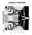
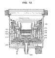
- FIGS. 12 and 13illustrate a modified version of the processing chamber of FIGS. 6 and 7 .
- FIGS. 14 and 15illustrate two embodiments of processing tools that may incorporate one or more processing stations constructed in accordance with the teachings of the present invention.
- a reactor for electrochemically processing at least one surface of a microelectronic workpiececomprises a reactor head including a workpiece support that has one or more electrical contacts positioned to make electrical contact with the microelectronic workpiece.
- the reactoralso includes a processing container having a plurality of nozzles angularly disposed in a sidewall of a principal fluid flow chamber at a level within the principal fluid flow chamber below a surface of a bath of processing fluid normally contained therein during electrochemical processing.
- a plurality of anodesare disposed at different elevations in the principal fluid flow chamber so as to place them at different distances from a microelectronic workpiece under process without an intermediate diffuser between the plurality of anodes and the microelectronic workpiece under process.
- One or more of the plurality of anodesmay be in close proximity to the workpiece under process. Still further, one or more of the plurality of anodes may be a virtual anode.
- the present inventionalso relates to multi-level anode configurations within a principal fluid flow chamber and methods of using the same.
- a reactor assembly 20 for electroplating a microelectronic workpiece 25such as a semiconductor wafer.
- the reactor assembly 20is comprised of a reactor head 30 and a corresponding reactor base, shown generally at 37 and described in substantial detail below, in which the electroplating solution is disposed.
- the reactor of FIG. 1Bcan also be used to implement electrochemical processing operations other than electroplating (e.g., electropolishing, anodization, etc.).
- the reactor head 30 of the electroplating reactor assemblymay comprised of a stationary assembly 70 and a rotor assembly 75 .
- Rotor assembly 75is configured to receive and carry an associated microelectronic workpiece 25 , position the microelectronic workpiece in a process-side down orientation within a container of reactor base 37 , and to rotate or spin the workpiece while joining its electrically-conductive surface in the plating circuit of the reactor assembly 20 .
- the rotor assembly 75includes one or more cathode contacts that provide electroplating power to the surface of the microelectronic workpiece.
- a cathode contact assemblyis shown generally at 85 and is described in further detail below. It will be recognized, however, that backside contact may be implemented in lieu of front side contact when the substrate is conductive or when an alternative electrically conductive path is provided between the back side of the microelectronic workpiece and the front side thereof.
- the reactor head 30is typically mounted on a lift/rotate apparatus which is configured to rotate the reactor head 30 from an upwardly-facing disposition in which it receives the microelectronic workpiece to be plated, to a downwardly facing disposition in which the surface of the microelectronic workpiece to be plated is positioned so that it may be brought into contact with the electroplating solution in reactor base 37 , either planar or at a given angle.
- a robotic armwhich preferably includes an end effector, is typically employed for placing the microelectronic workpiece 25 in position on the rotor assembly 75 , and for removing the plated microelectronic workpiece from within the rotor assembly.
- the contact assembly 85may be operated between an open state that allows the microelectronic workpiece to be placed on the rotor assembly 75 , and a closed state that secures the microelectronic workpiece to the rotor assembly and brings the electrically conductive components of the contact assembly 85 into electrical engagement with the surface of the microelectronic workpiece that is to be plated.
- FIG. 2illustrates the basic construction of processing base 37 and a corresponding computer simulation of the flow velocity contour pattern resulting from the processing container construction.
- the processing base 37generally comprises a main fluid flow chamber 505 , an antechamber 510 , a fluid inlet 515 , a plenum 520 , a flow diffuser 525 separating the plenum 520 from the antechamber 510 , and a nozzle slot assembly 530 separating the plenum 520 from the main chamber 505 .
- These componentscooperate to provide a flow of electrochemical processing fluid (here, of the electroplating solution) at the microelectronic workpiece 25 that has a substantially radially independent normal component.
- the impinging flowis centered about central axis 537 and possesses a nearly uniform component normal to the surface of the microelectronic workpiece 25 . This results in a substantially uniform mass flux to the microelectronic workpiece surface that, in turn, enables substantially uniform processing thereof.
- this desirable flow characteristicis achieved without the use of a diffuser disposed between the anode(s) and surface of the microelectronic workpiece that is to be electrochemically processed (e.g., electroplated).
- the anodes used in the electroplating reactorcan be placed in close proximity to the surface of the microelectronic workpiece to thereby provide substantial control over local electrical field/current density parameters used in the electroplating process.
- This substantial degree of control over the electrical parametersallows the reactor to be readily adapted to meet a wide range of electroplating requirements (e.g., seed layer thickness, seed layer type, electroplated material, electrolyte bath properties, etc.) without a corresponding change in the reactor hardware. Rather, adaptations can be implemented by altering the electrical parameters used in the electroplating process through, for example, software control of the power provided to the anodes.
- the reactor designthus effectively de-couples the fluid flow from adjustments to the electric field.
- An advantage of this approachis that a chamber with nearly ideal flow for electroplating and other electrochemical processes (i.e., a design which provides a substantially uniform diffusion layer across the microelectronic workpiece) may be designed that will not be degraded when electroplating or other electrochemical process applications require significant changes to the electric field.
- the diffusermust be moved closer to the surface of the workpiece if the distance between the anode and the workpiece surface is to be reduced.
- moving the diffuser closer to the workpiecesignificantly alters the flow characteristics of the electroplating fluid at the surface of the workpiece. More particularly, the close proximity between the diffuser and the surface of the workpiece introduces a corresponding increase in the magnitude of the normal components of the flow velocity at local areas 8 .
- the anodecannot be moved so that it is in close proximity to the surface of the microelectronic workpiece that is to be electroplated without introducing substantial diffusion layer control problems and undesirable localized increases in the electrical field corresponding to the pattern of apertures in the diffuser. Since the anode cannot be moved in close proximity to the surface of the microelectronic workpiece, the advantages associated with increased control of the electrical characteristics of the electrochemical process cannot be realized. Still further, movement of the diffuser to a position in close proximity with the microelectronic workpiece effectively generates a plurality of virtual anodes defined by the hole pattern of the diffuser. Given the close proximity of these virtual anodes to the microelectronic workpiece surface, the virtual anodes have a highly localized effect.
- electroplating solutionis provided through inlet 515 disposed at the bottom of the base 37 .
- the fluid from the inlet 515is directed therefrom at a relatively high velocity through antechamber 510 .
- antechamber 510includes an acceleration channel 540 through which the electroplating solution flows radially from the fluid inlet 515 toward fluid flow region 545 of antechamber 510 .
- Fluid flow region 545has a generally inverted U-shaped cross-section that is substantially wider at its outlet region proximate flow diffuser 525 than at its inlet region proximate channel 540 .
- This variation in the cross-sectionassists in removing any gas bubbles from the electroplating solution before the electroplating solution is allowed to enter the main chamber 505 .
- Gas bubbles that would otherwise enter the main chamber 505are allowed to exit the processing base 37 through a gas outlet (not illustrated in FIG. 2 , but illustrated in the embodiment shown in FIGS. 3-5 ) disposed at an upper portion of the antechamber 510 .
- Electroplating solution within antechamber 510is ultimately supplied to main chamber 505 .
- the electroplating solutionis first directed to flow from a relatively high-pressure region 550 of the antechamber 510 to the comparatively lower-pressure plenum 520 through flow diffuser 525 .
- Nozzle assembly 530includes a plurality of nozzles or slots 535 that are disposed at a slight angle With respect to horizontal. Electroplating solution exits plenum 520 through nozzles 535 with fluid velocity components in the vertical and radial directions.
- Main chamber 505is defined at its upper region by a contoured sidewall 560 and a slanted sidewall 565 .
- the contoured sidewall 560assists in preventing fluid flow separation as the electroplating solution exits nozzles 535 (particularly the uppermost nozzle(s)) and turns upward toward the surface of microelectronic workpiece 25 . Beyond breakpoint 570 , fluid flow separation will not substantially affect the uniformity of the normal flow.
- sidewall 565can generally have any shape, including a continuation of the shape of contoured sidewall 560 . In the specific embodiment disclosed here, sidewall 565 is slanted and, as will be explained in further detail below, is used to support one or more anodes.
- Electroplating solutionexits from main chamber 505 through a generally annular outlet 572 .
- Fluid exiting outlet 572may be provided to a further exterior chamber for disposal or may be replenished for re-circulation through the electroplating solution supply system.
- the processing base 37is also provided with one or more anodes.
- a principal anode 580is disposed in the lower portion of the main chamber 505 . If the peripheral edges of the surface of the microelectronic workpiece 25 extend radially beyond the extent of contoured sidewall 560 , then the peripheral edges are electrically shielded from principal anode 580 and reduced plating will take place in those regions.
- a plurality of annular anodes 585are disposed in a generally concentric manner on slanted sidewall 565 to provide a flow of electroplating current to the peripheral regions.
- Anodes 580 and 585 of the illustrated embodimentare disposed at different distances from the surface of the microelectronic as workpiece 25 that is being electroplated. More particularly, the anodes 580 and 585 are concentrically disposed in different horizontal planes. Such a concentric arrangement combined with the vertical differences allow the anodes 580 and 585 to be effectively placed close to the surface of the microelectronic workpiece 25 without generating a corresponding adverse impact on the flow pattern as tailored by nozzles 535 .
- an anode that is effectively spaced a given distance from the surface of microelectronic workpiece 25will have an impact on a larger area of the microelectronic workpiece surface than an anode that is effectively spaced from the surface of microelectronic workpiece 25 by a lesser amount.
- Anodes that are effectively spaced at a comparatively large distance from the surface of microelectronic workpiece 25thus have less localized control over the electroplating process than do those that are spaced at a smaller distance.
- anode 580is effectively “seen” by microelectronic workpiece 25 as being positioned an approximate distance A 1 from the surface of microelectronic workpiece 25 .
- anodes 585are approximately at effective distances A 2 , A 3 , and A 4 proceeding from the innermost anode to the outermost anode, with the outermost anode being closest to the microelectronic workpiece 25 .
- All of the anodes 585are in close proximity (i.e., about 25.4 mm or less, with the outermost anode being spaced from the microelectronic workpiece by about 10 mm) to the surface of the microelectronic workpiece 25 that is being electroplated. Since anodes 585 are in close proximity to the surface of the microelectronic workpiece 25 , they can be used to provide effective, localized control over the radial film growth at peripheral portions of the microelectronic workpiece.
- Such localized controlis particularly desirable at the peripheral portions of the microelectronic workpiece since it is those portions that are more likely to have a high uniformity gradient (most often due to the fact that electrical contact is made with the seed layer of the microelectronic workpiece at the outermost peripheral regions resulting in higher plating rates at the periphery of the microelectronic workpiece compared to the central portions thereof).
- the electroplating power provided to the foregoing anode arrangementcan be readily controlled to accommodate a wide range of plating requirements without the need for a corresponding hardware modification.
- Some reasons for adjusting the electroplating powerinclude changes to the following:
- the foregoing anode arrangementis particularly well-suited for plating microelectronic workpieces having highly resistive seed layers as well as for plating highly resistive materials on microelectronic workpieces.
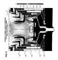
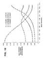
- the more resistive the seed layer or material that is to be depositedthe more the magnitude of the current at the central anode 580 (or central anodes) should be increased to yield a uniform film. This effect can be understood in connection with an example and the set of corresponding graphs set forth in FIGS. 10 and 11 .
- FIG. 10is a graph of four different computer simulations reflecting the change in growth of an electroplated film versus the radial position across the surface of a microelectronic workpiece.
- the graphillustrates the changing growth that occurs when the current to a given one of the four anodes 580 , 585 is changed without a corresponding change in the current to the remaining anodes.
- Anode 1corresponds to anode 580 and the remaining Anodes 2 through 4 correspond to anodes 585 proceeding from the interior most anode to the outermost anode.
- the peak plating for each anodeoccurs at a different radial position.
- anode 580being effectively at the largest distance from the surface of the workpiece, has an effect over a substantial radial portion of the workpiece and thus has a broad affect over the surface area of the workpiece.
- the remaining anodeshave substantially more localized effects at the radial positions corresponding to the peaks of the graph of FIG. 10 .
- each of the anodes 580 , 585may be provided with a fixed current that may differ from the current provided to the remaining anodes. These plating current differences can be provided to compensate for the increased plating that generally occurs at the radial position of the workpiece surface proximate the contacts of the cathode contact assembly 85 ( FIG. 1B ).
- FIG. 11The computer simulated effect of a predetermined set of plating current differences on the normalized thickness of the electroplated film as a function of the radial position on the microelectronic workpiece over time is shown in FIG. 11 .
- the seed layerwas assumed to be uniform at t 0 .
- FIG. 11The computer simulated effect of a predetermined set of plating current differences on the normalized thickness of the electroplated film as a function of the radial position on the microelectronic workpiece over time is shown in FIG. 11 .
- the seed layerwas assumed to be uniform at t 0 .
- the differential plating that results from the differential current provided to the anodes 580 , 585forms a substantially uniform plated film by the end of the electroplating process. It will be recognized that the particular currents that are to be provided to anodes 580 , 585 depends upon numerous factors including, but not necessarily limited to, the desired thickness and material of the electroplated film, the thickness and material of the initial seed layer, the distances between anodes 580 , 585 and the surface of the microelectronic workpiece, electrolyte bath properties, etc.
- Anodes 580 , 585may be consumable, but are preferably inert and formed from platinized titanium or some other inert conductive material. However, as noted above, inert anodes tend to evolve gases that can impair the uniformity of the plated film. To reduce this problem, as well as to reduce the likelihood of the entry of bubbles into the main processing chamber 505 , processing base 37 includes several unique features. With respect to anode 580 , a small fluid flow path forms a Venturi outlet 590 between the underside of anode 580 and the relatively lower pressure channel 540 (see FIG. 2 ).
- the Venturi flow path 590may be shielded to prevent any large bubbles originating from outside the chamber from rising through region 590 . Instead, such bubbles enter the bubble-trapping region of the antechamber 510 .
- electroplating solutionsweeps across the surfaces of anodes 585 in a radial direction toward fluid outlet 572 to remove gas bubbles forming at their surfaces. Further, the radial components of the fluid flow at the surface of the microelectronic workpiece assist in sweeping gas bubbles therefrom.
- the flow through the nozzles 535is directed away from the microelectronic workpiece surface and, as such, there are no jets of fluid created to disturb the uniformity of the diffusion layer.
- the diffusion layermay not be perfectly uniform, it will be substantially uniform, and any non-uniformity will be relatively gradual as a result. Further, the effect of any minor non-uniformity may be substantially reduced by rotating the microelectronic workpiece during processing.
- a further advantagerelates to the flow at the bottom of the main chamber 505 that is produced by the Venturi outlet, which influences the flow at the centerline thereof. The centerline flow velocity is otherwise difficult to implement and control. However, the strength of the Venturi flow provides a non-intrusive design variable that may be used to affect this aspect of the flow.
- the flow that is normal to the microelectronic workpiecehas a slightly greater magnitude near the center of the microelectronic workpiece and creates a dome-shaped meniscus whenever the microelectronic workpiece is not present (i.e., before the microelectronic workpiece is lowered into the fluid).
- the dome-shaped meniscusassists in minimizing bubble entrapment as the microelectronic workpiece or other workpiece is lowered into the processing solution (here, the electroplating solution).
- a still further advantage of the foregoing reactor designis that it assists in preventing bubbles that find their way to the chamber inlet from reaching the microelectronic workpiece.
- the flow patternis such that the solution travels downward just before entering the main chamber. As such, bubbles remain in the antechamber and escape through holes at the top thereof. Further, the upward sloping inlet path (see FIG. 5 and appertaining description) to the antechamber prevents bubbles from entering the main chamber through the Venturi flow path.
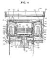
- FIGS. 3-5illustrate a specific construction of a complete processing chamber assembly 610 that has been specifically adapted for electrochemical processing of a semiconductor microelectronic workpiece. More particularly, the illustrated embodiment is specifically adapted for depositing a uniform layer of material on the surface of the workpiece using electroplating.
- processing base 37 shown in FIG. 1Bis comprised of processing chamber assembly 610 along with a corresponding exterior cup 605 .
- Processing chamber assembly 610is disposed % within exterior cup 605 to allow exterior cup 605 to receive spent processing fluid that overflows from the processing chamber assembly 610 .
- a flange 615extends about the assembly 610 for securement with, for example, the frame of the corresponding tool.
- the flange of the exterior cup 605is formed to engage or otherwise accept rotor assembly 75 of reactor head 30 (shown in FIG. 1B ) and allow contact between the microelectronic workpiece 25 and the processing solution, such as electroplating solution, in the main fluid flow chamber 505 .
- the exterior cup 605also includes a main cylindrical housing 625 into which a drain cup member 627 is disposed.
- the drain cup member 627includes an outer surface having channels 629 that, together with the interior wall of main cylindrical housing 625 , form one or more helical flow chambers 640 that serve as an outlet for the processing solution.
- Processing fluid overflowing a weir member 739 at the top of processing cup 35drains through the helical flow chambers 640 and exits an outlet (not illustrated) where it is either disposed of or replenished and re-circulated.
- This configurationis particularly suitable for systems that include fluid re-circulation since it assists in reducing the mixing of gases with the processing solution thereby further reducing the likelihood that gas bubbles will interfere with the uniformity of the diffusion layer at the workpiece surface.
- antechamber 510is defined by the walls of a plurality of separate components. More particularly, antechamber 510 is defined by the interior walls of drain cup member 627 , an anode support member 697 , the interior and exterior walls of a mid-chamber member 690 , and the exterior walls of flow diffuser 525 .
- FIGS. 3B and 4illustrate the manner in which the foregoing components are brought together to form the reactor.
- the mid-chamber member 690is disposed interior of the drain cup member 627 and includes a plurality of leg supports 692 that sit upon a bottom wall thereof.
- the anode support member 697includes an outer wall that engages a flange that is disposed about the interior of drain cup member 627 .
- the anode support member 697also includes a channel 705 that sits upon and engages an upper portion of flow diffuser 525 , and a further channel 710 that sits upon and engages an upper rim of nozzle assembly 530 .
- Mid-chamber member 690also includes a centrally disposed receptacle 715 that is dimensioned to accept the lower portion of nozzle assembly 530 .
- an annular channel 725is disposed radially exterior of the annular receptacle 715 to engage a lower portion of flow diffuser 525 .
- the flow diffuser 525is formed as a single piece and includes a plurality of vertically oriented slots 670 .
- the nozzle assembly 530is formed as a single piece and includes a plurality of horizontally oriented slots that constitute the nozzles 535 .
- the anode support member 697includes a plurality of annular grooves that are dimensioned to accept corresponding annular anode assemblies 785 .
- Each anode assembly 785includes an anode 585 (preferably formed from platinized titanium or another inert metal) and a conduit 730 extending from a central portion of the anode 585 through which a metal conductor may be disposed to electrically connect the anode 585 of each assembly 785 to an external source of electrical power.
- Conduit 730is shown to extend entirely through the processing chamber assembly 610 and is secured at the bottom thereof by a respective fitting 733 .
- anode assemblies 785effectively urge the anode support member 697 downward to clamp the flow diffuser 525 , nozzle assembly 530 , mid-chamber member 690 , and drain cup member 627 against the bottom portion 737 of the exterior cup 605 .
- Thisallows for easy assembly and disassembly of the processing chamber 610 .
- other meansmay be used to secure the chamber elements together as well as to conduct the necessary electrical power to the anodes.
- the illustrated embodimentalso includes a weir member 739 that detachably snaps or otherwise easily secures to the upper exterior portion of anode support member 697 .
- weir member 739includes a rim 742 that forms a weir over which the processing solution flows into the helical flow chamber 640 .
- Weir member 739also includes a transversely extending flange 744 that extends radially inward and forms an electric field shield over all or portions of one or more of the anodes 585 . Since the weir member 739 may be easily removed and replaced, the processing chamber assembly 610 may be readily reconfigured and adapted to provide different electric field shapes. Such differing electrical field shapes are particularly useful in those instances in which the reactor must be configured to process more than one size or shape of a workpiece. Additionally, this allows the reactor to be configured to accommodate workpieces that are of the same size, but have different plating area requirements.
- the anode support member 697forms the contoured sidewall 560 and slanted sidewall 565 that is illustrated in FIG. 2 .
- the lower region of anode support member 697is contoured to define the upper interior wall of antechamber 510 and preferably includes one or more gas outlets 665 that are disposed therethrough to allow gas bubbles to exit from the antechamber 510 to the exterior environment.
- fluid inlet 515is defined by an inlet fluid guide, shows generally at 810 , that is secured to the floor of mid-chamber member 690 by one or more fasteners 815 .
- Inlet fluid guide 810includes a plurality of open channels 817 that guide fluid received at fluid inlet 515 to an area beneath mid-chamber member 690 .
- Channels 817 of the illustrated embodimentare defined by upwardly angled walls 819 . Processing fluid exiting channels 817 flows therefrom to one or more further channels 821 that are likewise defined by walls that angle upward.
- Central anode 580includes an electrical connection rod 581 that proceeds to the exterior of the processing chamber assembly 610 through central apertures formed in nozzle assembly 530 , mid-chamber member 690 and inlet fluid guide 810 .
- the small Venturi flow path regions shown at 590 in FIG. 2are formed in FIG. 5 by vertical channels 823 that proceed through drain cup member 690 and the bottom wall of nozzle member 530 .
- the fluid inlet guide 810 and, specifically, the upwardly angled walls 819extend radially beyond the shielded vertical channels 823 so that any, bubbles entering the inlet proceed through the upward channels 821 rather than through the vertical channels 823 .
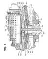
- FIGS. 6-9illustrate a further embodiment of an improved reactor chamber.
- the embodiment illustrated in these figuresretains the advantageous electric field and flow characteristics of the foregoing reactor construction while concurrently being useful for situations in which anode/electrode isolation is desirable.
- Such situationsinclude, but are not limited to, the following:
- the reactorincludes an electrochemical electroplating solution flow path into the innermost portion of the processing chamber that is very similar to the flow path of the embodiment illustrated in FIG. 2 and as implemented in the embodiment of the reactor chamber shown in FIGS. 3A through 5 .
- components that have similar functionsare not further identified here for the sake of simplicity. Rather, only those portions of the reactor that significantly) differ from the foregoing embodiment are identified and described below.
- the reactor based 37includes a plurality of ring-shaped anodes 1015 , 1020 , 1025 and 1030 that are concentrically disposed with respect to one another in respective anode chamber housings 1017 , 1022 , 1027 and 1032 .
- each anode 1015 , 1020 , 1025 and 1030has a vertically oriented surface area that is greater than the surface area of the corresponding anodes shown in the foregoing embodiments.
- Four such anodesare employed in the disclosed embodiment, but a larger or smaller number of anodes may be used depending upon the electrochemical processing parameters and results that are desired.
- Each anode 1015 , 1020 , 1025 and 1030is supported in the respective anode chamber housing 1017 , 1022 , 1027 and 1032 by at least one corresponding support/conductive member 1050 that extends through the bottom of the processing base 37 and terminates at an electrical connector 1055 for connection to an electrical power source.
- fluid flow to and through the three outer most chamber housings 1022 , 1027 and 1032is provided from an inlet 1060 that is separate from inlet 515 , which supplies the fluid flow through an innermost chamber housing 1017 .
- fluid inlet 1060provides electroplating solution to a manifold 1065 having a plurality of slots 1070 disposed in its exterior wall. Slots 1070 are in fluid communication with a plenum 1075 that includes a plurality of openings 1080 through which the electroplating solution respectively enters the three anode chamber housings 1022 , 1027 and 1032 .
- Fluid entering the anode chamber housings 1017 , 1022 , 1027 and 1032flows over at least one vertical surface and, preferably, both vertical surfaces of the respective anode 1015 , 1020 , 1025 and 1030 .
- Each anode chamber housing 1017 , 1022 , 1027 and 1032includes an upper outlet region that opens to a respective cup 1085 .
- Cups 1085are disposed in the reactor chamber so that they are concentric with one another.
- Each cupincludes an upper rim 1090 that terminates at a predetermined height with respect to the other rims, with the rim of each cup terminating at a height that is vertically below the immediately adjacent outer concentric cup.
- Each of the three innermost cupsfurther includes a substantially vertical exterior wall 1095 and a slanted interior wall 1200 .
- This wall constructioncreates a flow region 1205 in the interstitial region between concentrically disposed cups (excepting the innermost cup that has a contoured interior wall that defines the fluid flow region 1205 and than the outer most flow region 1205 associated with the outer most anode) that increases in area as the fluid flows upward toward the surface of the microelectronic workpiece under process.
- the increase in areaeffectively reduces the fluid flow velocity along the vertical fluid flow path, with the velocity being greater at a lower portion of the flow region 1205 when compared to the velocity of the fluid flow at the upper portion of the particular flow region.
- the interstitial region between the rims of concentrically adjacent cupseffectively defines the size and shape of each of a plurality of virtual anodes, each virtual anode being respectively associated with a corresponding anode disposed in its respective anode chamber housing.
- the size and shape of each virtual anode that is seen by the microelectronic workpiece under processis generally independent of the size and shape of the corresponding actual anode.
- consumable anodesthat vary in size and shape over time as they are used can be employed for anodes 1015 , 1020 , 1025 and 1030 without a corresponding change in the overall anode configuration is seen by the microelectronic workpiece under process.
- a high fluid flow velocitymay be introduced across the vertical surfaces of the anodes 1015 , 1020 , 1025 and 1030 in the anode chamber housings 1022 , 1027 and 1032 while concurrently producing a very uniform fluid flow pattern radially across the surface of the microelectronic workpiece under process.
- Such a high fluid flow velocity across the vertical surfaces of the anodes 1015 , 1020 , 1025 and 1030is desirable when using certain electrochemical electroplating solutions, such as electroplating fluids available from Atotech.
- each of the anode chamber housings 1017 , 1022 , 1027 and 1032may be provided with one or more gas outlets (not illustrated) at the upper portion thereof to vent such gases.
- element 1210is a securement that is formed from a dielectric material.
- the securement 1210is used to clamp a plurality of the structures forming reactor base 37 together.
- securement 1210may be formed from a conductive material so that it may function as an anode, the innermost anode seen by the microelectronic workpiece under process is preferably a virtual anode corresponding to the interior most anode 1015 .
- FIGS. 8 and 9illustrate computer simulations of fluid flow velocity contours of a reactor constructed in accordance with the embodiment shown in FIGS. 10 through 12 .
- all of the anodes of the reactor basemay be isolated from a flow of fluid through the anode chamber housings.
- FIG. 8illustrates the fluid flow velocity contours that occur when a floss of electroplating solution is provided through each of the anode chamber housings
- FIG. 9illustrates the fluid flow velocity contours that occur when there is no flow of electroplating solution provided through the anode chamber housings past the anodes.
- This latter conditioncan be accomplished in the reactor of by turning off the flow the flow from the second fluid flow inlet (described below) and may likewise be accomplished in the reactor of FIGS. 6 and 7 by turning of the fluid flow through inlet 1060 .
- Such a conditionmay be desirable in those instances in which a flow of electroplating solution across the surface of the anodes is found to significantly reduce the organic additive concentration of the solution.
- FIG. 12illustrates a variation of the reactor embodiment shown in FIG. 7 .
- FIG. 12illustrates a variation of the reactor embodiment shown in FIG. 7 .
- elements pertinent to the following discussionare provided with reference numerals.
- This further embodimentemploys a different structure for providing fluid flow to the anodes 1015 , 1020 , 1025 and 1030 . More particularly, the further embodiment employs an inlet member 2010 that serves as an inlet for the supply and distribution of the processing fluid to the anode chamber housings 1017 , 1022 , 1027 and 1032 .
- the inlet member 2010includes a hollow stem 2015 that may be used to provide a flow of electroplating fluid.
- the hollow stem 2015terminates at a stepped hub 2020 .
- Stepped hub 2020includes a plurality of steps 2025 that each include a groove dimensioned to receive and support a corresponding wall of the anode chamber housings. Processing fluid is directed into the anode chamber housings through a plurality of channels 2030 that proceed from a manifold area into the respective anode chamber housing.
- This latter inlet arrangementassists in further electrically isolating anodes 1015 , 1020 , 1025 and 1030 from one another.
- Such electrical isolationoccurs due to the increased resistance of the electrical flow path between the anodes.
- the increased resistanceis a direct result of the increased length of the fluid flow paths that exist between the anode chamber housings.
- the manner in which the electroplating power is supplied to the microelectronic workpiece at the peripheral edge thereofeffects the overall film quality of the deposited metal.
- Some of the more desirable characteristics of a contact assembly used to provide such electroplating powerinclude, for example, the following:
- reactor assembly 20preferably employs a contact assembly 85 that provides either a continuous electrical contact or a high number of discrete electrical contacts with the microelectronic workpiece 25 .
- a contact assembly 85that provides either a continuous electrical contact or a high number of discrete electrical contacts with the microelectronic workpiece 25 .
- Contact assembly 85includes contact members that provide minimal intrusion about the microelectronic workpiece periphery while concurrently providing consistent contact with the seed layer.
- Contact with the seed layeris enhanced by using a contact member structure that provides a wiping action against the seed layer as the microelectronic workpiece is brought into engagement with the contact assembly. This wiping action assists in removing any oxides at the seed layer surface thereby enhancing the electrical contact between the contact structure and the seed layer.
- uniformity of the current densities about the microelectronic workpiece peripheryare increased and the resulting film is more uniform. Further, such consistency in the electrical contact facilitates greater consistency in the electroplating process from wafer-to-wafer thereby increasing wafer-to-wafer uniformity.
- Contact assembly 85also preferably includes one or more structures that provide a barrier, individually or in cooperation with other structures that separates the contact/contacts, the peripheral edge portions and backside of the microelectronic workpiece 25 from the plating solution. This prevents the plating of metal onto the individual contacts and, further, assists in preventing any exposed portions of the barrier layer near the edge of the microelectronic workpiece 25 from being exposed to the electroplating environment. As a result, plating of the barrier layer and the appertaining potential for contamination due to flaking of any loosely adhered electroplated material is substantially limited. Exemplary contact assemblies suitable for use in the present system are illustrated in U.S. Ser. No. 09/113,723, while Jul. 10, 1998, entitled “PLATING APPARATUS WITH PLATING CONTACT WITH PERIPHERAL SEAL MEMBER”, which is hereby incorporated by reference.
- One or more of the foregoing reactor assembliesmay be readily integrated in a processing tool that is capable of executing a plurality of processes on a workpiece, such as a semiconductor microelectronic workpiece.
- a processing toolis the LT-210TM electroplating apparatus available from Semitool, Inc., of Kalispell, Mont.
- FIGS. 14 and 15illustrate such integration.
- the system of FIG. 14includes a plurality of processing stations 1610 .
- these processing stationsinclude one or more rinsing/drying stations and one or more electroplating stations (including one or more electroplating reactors such as the one above), although further immersion-chemical processing stations constructed in accordance with the of the present invention may also be employed.
- the systemalso preferably includes a thermal processing station, such as at 1615 , that includes at least one thermal reactor that is adapted for rapid thermal processing (RTP).
- RTPrapid thermal processing
- the workpiecesare transferred between the processing stations 1610 and the RTP station 1615 using one or more robotic transfer mechanisms 1620 that are disposed for linear movement along a central track 1625 .
- One or more of the stations- 1610may also incorporate structures that are adapted for executing an in-situ rinse.
- all of the processing stations as well as the robotic transfer mechanismsare disposed in a cabinet that is provided with filtered air at a positive pressure to thereby limit airborne contaminants that may reduce the effectiveness of the microelectronic workpiece processing.
- FIG. 15illustrates a further embodiment of a processing tool in which an RTP station 1635 , located in portion 1630 , that includes at least one thermal reactor, may be integrated in a tool set.
- at least one thermal reactoris serviced by a dedicated robotic mechanism 1640 .
- the dedicated robotic mechanism 1640accepts workpieces that are transferred to it by the robotic transfer mechanisms 1620 . Transfer may take place through an intermediate staging door/area 1645 . As such, it becomes possible to hygienically separate the RTP portion 1630 of the processing tool from other portions of the tool.
- the illustrated annealing stationmay be implemented as a separate module that is attached to upgrade an existing tool set. It will be recognized that other types of processing stations may be located in portion 1630 in addition to or instead of RTP station 1635 .
Landscapes
- Chemical & Material Sciences (AREA)
- Engineering & Computer Science (AREA)
- Chemical Kinetics & Catalysis (AREA)
- Electrochemistry (AREA)
- Materials Engineering (AREA)
- Metallurgy (AREA)
- Organic Chemistry (AREA)
- Life Sciences & Earth Sciences (AREA)
- Sustainable Development (AREA)
- Electroplating Methods And Accessories (AREA)
- Electrodes Of Semiconductors (AREA)
- Cleaning Or Drying Semiconductors (AREA)
Abstract
Description
This application is a continuation of U.S. application Ser. No. 10/715,700, filed Nov. 18, 2003 now abandoned, which is a continuation of U.S. application Ser. No. 09/804,697, filed Mar. 12, 2001, which issued on Dec. 9, 2003 as U.S. Pat. No. 6,660,137, which is a continuation of prior International Application No. PCT/US00/10120, filed Apr. 13, 2000 in the English language and published in the English language as International Publication No. WO 00/61498, which in turn claims priority to the following three U.S. Provisional Applications: U.S. Ser. No. 60/129,055, entitled “WORKPIECE PROCESSOR HAVING IMPROVED PROCESSING CHAMBER”, filed Apr. 13, 1999; U.S. Ser. No. 60/143,769, entitled “WORKPIECE PROCESSING HAVING IMPROVED PROCESSING CHAMBER,” filed Jul. 12, 1999; U.S. Ser. No. 60/182,160 entitled “WORKPIECE PROCESSOR HAVING IMPROVED PROCESSING CHAMBER”, filed Feb. 14, 2000. The entire disclosures of all three of the prior applications, as well as International Publication No. WO 00/61498, are incorporated herein by reference.
Not Applicable
The fabrication of microelectronic components from a microelectronic workpiece, such as a semiconductor wafer substrate, polymer substrate, etc., involves a substantial number of processes. For purposes of the present application, a microelectronic workpiece is defined to include a workpiece formed from a substrate upon which microelectronic circuits or components, data storage elements or layers, and/or micro-mechanical elements are formed. There are a number of different processing operations performed on the microelectronic workpiece to fabricate the microelectronic component(s). Such operations include, for example, material deposition, patterning, doping, chemical mechanical polishing, electropolishing, and heat treatment.
Material deposition processing involves depositing or otherwise forming thin layers of material on the surface of the microelectronic workpiece (hereinafter described as, but not limited to, a semiconductor wafer). Patterning provides removal of selected portions of these added layers. Doping of the semiconductor wafer, or similar microelectronic workpiece, is the process of adding impurities known as “dopants” to the selected portions of the wafer to alter the electrical characteristics of the substrate material. Heat treatment of the semiconductor wafer involves heating and/or cooling the wafer to achieve specific process results. Chemical mechanical polishing involves the removal of material through a combined chemical/mechanical process while electropolishing involves the removal of material from a workpiece surface using electrochemical reactions.
Numerous processing devices, known as processing “tools”, have been developed to implement the foregoing processing operations. These tools take on different configurations depending on the type of workpiece used in the fabrication process and the process or processes executed by the tool. One tool configuration, known as the LT-210C™ processing tool and available from Semitool, Inc., of Kalispell, Mont., includes a plurality of microelectronic workpiece processing stations that utilize a workpiece holder and a process bowl or container for implementing wet processing operations. Such wet processing operations include electroplating, etching, cleaning, electroless deposition, electropolishing, etc. In connection with the present invention, it is the electrochemical processing stations used in the LT-210C™ that are noteworthy. Such electrochemical processing stations perform the foregoing electroplating, electropolishing, anodization, etc., of the microelectronic workpiece. It will be recognized that the electrochemical processing system set forth herein is readily adapted to implement each of the foregoing electrochemical processes.
In accordance with one configuration of the LT-210C™ tool, the electroplating stations include a workpiece holder and a process container that are disposed proximate one another. The workpiece holder and process container are operated to bring the microelectronic workpiece held by the workpiece holder into contact with an electroplating fluid disposed in the process container to form a processing chamber. Restricting the electroplating solution to the appropriate portions of the workpiece, however, is often problematic. Additionally, ensuring proper mass transfer conditions between the electroplating solution and the surface of the workpiece can be difficult. Absent such mass transfer control, the electrochemical processing of the workpiece surface can often be non-uniform. This can be particularly problematic in connection with the electroplating of metals. Still further, control of the shape and magnitude of the electric field is increasingly important.
Conventional electrochemical reactors have utilized various techniques to bring the electroplating solution into contact as with the surface of the workpiece in a controlled manner. For example, the electroplating solution may be brought into contact with the surface of the workpiece using partial or full immersion processing in which the electroplating solution resides in a processing container and at least one surface of the workpiece is brought into contact with or below the surface of the electroplating solution.
Electroplating and other electrochemical processes have become important in the production of semiconductor integrated circuits and other microelectronic devices from microelectronic workpieces. For example, electroplating is often used in the formation of one or more metal layers on the workpiece. These metal layers are often used to electrically interconnect the various devices of the integrated circuit. Further, the structures formed from the metal layers may constitute microelectronic devices such as read/write heads, etc.
Electroplated metals typically include copper, nickel, gold, platinum, solder, nickel-iron, etc. Electroplating is generally, effected by initial formation of a seed layer on the microelectronic workpiece in the form of a very thin layer of metal, whereby the surface of the microelectronic workpiece is rendered electrically conductive. This electro-conductivity permits subsequent formation of a blanket or patterned layer of the desired metal by electroplating. Subsequent processing, such as chemical mechanical planarization, may be used to remove unwanted portions of the patterned or metal blanket layer formed during electroplating, resulting in the formation of the desired metallized structure.
Electropolishing of metals at the surface of a workpiece involves the removal of at least some of the metal using an electrochemical process. The electrochemical process is effectively the reverse of the electroplating reaction and is often carried out using the same or similar reactors as electroplating.
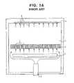
Existing electroplating processing containers often provide a continuous flow of electroplating solution to the electroplating chamber through a single inlet disposed at the bottom portion of the chamber. One embodiment of such a processing container is illustrated inFIG. 1A . As illustrated, the electroplating reactor, shown generally at1, includes aelectroplating processing container 2 that is used to contain a flow of electroplating solution provided through afluid inlet 3 disposed at a lower portion of thecontainer 2. In such a reactor, the electroplating solution completes an electrical circuit path between an anode4 and a surface ofworkpiece 5, which functions as a cathode.
The electroplating reactions that take place at the surface of the microelectronic workpiece are dependent on species mass transport (e.g., copper ions, platinum ions, gold ions, etc.) to the microelectronic workpiece surface through a diffusion layer (a.k.a. mass transport layer) that forms proximate the microelectronic workpiece's surface. It is desirable to have a diffusion layer that is both thin and uniform over the surface of the microelectronic workpiece if a uniform electroplated film is to be deposited within a reasonable amount of time.
Even distribution of the electroplating solution over the workpiece surface to control the thickness and uniformity of the diffusion layer in the processing container ofFIG. 1A is facilitated, for example, by adiffuser 6 or the like that is disposed between the single inlet and the workpiece surface. The diffuser includes a plurality of apertures7 that are provided to disburse the stream of electroplating fluid provided from theprocessing fluid inlet 3 as evenly as possible across the surface of theworkpiece 5.
Although substantial improvements in diffusion layer control result from the use of a diffuser, such control is limited. With reference toFIG. 1A , localizedareas 8 of increased flow velocity normal to the surface of the microelectronic workpiece are often generated by thediffuser 6. These localized areas generally correspond to the position of apertures7 of thediffuser 6. This effect is increased as thediffuser 6 is moved closer to the workpiece.
The present inventors have found that these localized areas of increased flow velocity at the surface of the workpiece affect the diffusion layer conditions and can result in non-uniform deposition of the electroplated material over the surface of the workpiece. Diffuser hole pattern configurations also affect the distribution of the electric field since the diffuser is disposed between the anode and workpiece, and can result in non-uniform deposition of the electroplated material. In the reactor illustrated inFIG. 1A , the electric field tends to be concentrated atlocalized areas 8 corresponding to the apertures in the diffuser. These effects in thelocalized areas 8 are dependent on diffuser distance from the workpiece and the diffuser hole size and pattern.
Another problem often encountered in electroplating is disruption of the diffusion layer due to the entrapment and evolvement of gasses during the electroplating process. For example, bubbles can be created in the plumbing and pumping system of the processing equipment. Electroplating is thus inhibited at those sites on the surface of the workpiece to which the bubbles migrate. Gas evolvement is particularly a concern when an inert anode is utilized since inert anodes tend to generate gas bubbles as a result of the anodic reactions that take place at the anode's surface.
Consumable anodes are often used to reduce the evolvement of gas bubbles in the electroplating solution and to maintain bath stability. However, consumable anodes frequently have a passivated film surface that must be maintained. They also erode into the plating solution changing the dimensional tolerances. Ultimately, the) must be replaced thereby increasing the amount of maintenance required to keep the tool operational when compared to tools using inert anodes.
Another challenge associated with the plating of uniform films is the changing resistance of the plated film. The initial seed layer can have a high resistance and this resistance decreases as the film becomes thicker. The changing resistance makes it difficult for a given set of chamber hardware to yield optimal uniformity on a variety of seed layers and deposited film thicknesses.
In view of the foregoing, the present inventors have developed a system for electrochemically processing a microelectronic workpiece that can readily adapt to a wide range of electrochemical processing requirements (e.g., seed layer thicknesses, seed layer types, electroplating materials, electrolyte bath properties, etc.). The system can adapt to such electrochemical processing requirements while concurrently providing a controlled, substantially uniform diffusion layer at the surface of the workpiece that assists in providing a corresponding substantially uniform processing of the workpiece surface (e.g., uniform deposition of the electroplated material).
A reactor for electrochemically processing at least one surface of a microelectronic workpiece is set forth. The reactor comprises a reactor head including a workpiece support that has one or more electrical contacts positioned to make electrical contact with the microelectronic workpiece. The reactor also includes a processing container having a plurality of nozzles angularly disposed in a sidewall of a principal fluid flow chamber at a level within the principal fluid flow chamber below a surface of a bath of processing fluid normally contained therein during electrochemical processing. A plurality of anodes are disposed at different elevations in the principal fluid flow chamber so as to place them at different distances from a microelectronic workpiece under process without an intermediate diffuser between the plurality of anodes and the microelectronic workpiece under process. One or more of the plurality of anodes may be in close proximity to the workpiece under process. Still further, one or more of the plurality of anodes may be a virtual anode. The present invention also relates to multi-level anode configurations within a principal fluid flow chamber and methods of using the same.
Basic Reactor Components
With reference toFIG. 1B , there is shown areactor assembly 20 for electroplating amicroelectronic workpiece 25, such as a semiconductor wafer. Generally stated, thereactor assembly 20 is comprised of areactor head 30 and a corresponding reactor base, shown generally at37 and described in substantial detail below, in which the electroplating solution is disposed. The reactor ofFIG. 1B can also be used to implement electrochemical processing operations other than electroplating (e.g., electropolishing, anodization, etc.).
Thereactor head 30 of the electroplating reactor assembly may comprised of astationary assembly 70 and arotor assembly 75.Rotor assembly 75 is configured to receive and carry an associatedmicroelectronic workpiece 25, position the microelectronic workpiece in a process-side down orientation within a container ofreactor base 37, and to rotate or spin the workpiece while joining its electrically-conductive surface in the plating circuit of thereactor assembly 20. Therotor assembly 75 includes one or more cathode contacts that provide electroplating power to the surface of the microelectronic workpiece. In the illustrated embodiment, a cathode contact assembly is shown generally at85 and is described in further detail below. It will be recognized, however, that backside contact may be implemented in lieu of front side contact when the substrate is conductive or when an alternative electrically conductive path is provided between the back side of the microelectronic workpiece and the front side thereof.
Thereactor head 30 is typically mounted on a lift/rotate apparatus which is configured to rotate thereactor head 30 from an upwardly-facing disposition in which it receives the microelectronic workpiece to be plated, to a downwardly facing disposition in which the surface of the microelectronic workpiece to be plated is positioned so that it may be brought into contact with the electroplating solution inreactor base 37, either planar or at a given angle. A robotic arm, which preferably includes an end effector, is typically employed for placing themicroelectronic workpiece 25 in position on therotor assembly 75, and for removing the plated microelectronic workpiece from within the rotor assembly. Thecontact assembly 85 may be operated between an open state that allows the microelectronic workpiece to be placed on therotor assembly 75, and a closed state that secures the microelectronic workpiece to the rotor assembly and brings the electrically conductive components of thecontact assembly 85 into electrical engagement with the surface of the microelectronic workpiece that is to be plated.
It will be recognized that other reactor assembly configurations may be used with the inventive aspects of the disclosed reactor chamber, the foregoing being merely illustrative.
Electrochemical Processing Container
Notably, as will be clear from the description below, this desirable flow characteristic is achieved without the use of a diffuser disposed between the anode(s) and surface of the microelectronic workpiece that is to be electrochemically processed (e.g., electroplated). As such, the anodes used in the electroplating reactor can be placed in close proximity to the surface of the microelectronic workpiece to thereby provide substantial control over local electrical field/current density parameters used in the electroplating process. This substantial degree of control over the electrical parameters allows the reactor to be readily adapted to meet a wide range of electroplating requirements (e.g., seed layer thickness, seed layer type, electroplated material, electrolyte bath properties, etc.) without a corresponding change in the reactor hardware. Rather, adaptations can be implemented by altering the electrical parameters used in the electroplating process through, for example, software control of the power provided to the anodes.
The reactor design thus effectively de-couples the fluid flow from adjustments to the electric field. An advantage of this approach is that a chamber with nearly ideal flow for electroplating and other electrochemical processes (i.e., a design which provides a substantially uniform diffusion layer across the microelectronic workpiece) may be designed that will not be degraded when electroplating or other electrochemical process applications require significant changes to the electric field.
The foregoing advantages can be more greatly appreciated through a comparison with the prior art reactor design illustrated inFIG. 1A . In that design, the diffuser must be moved closer to the surface of the workpiece if the distance between the anode and the workpiece surface is to be reduced. However, moving the diffuser closer to the workpiece significantly alters the flow characteristics of the electroplating fluid at the surface of the workpiece. More particularly, the close proximity between the diffuser and the surface of the workpiece introduces a corresponding increase in the magnitude of the normal components of the flow velocity atlocal areas 8. As such, the anode cannot be moved so that it is in close proximity to the surface of the microelectronic workpiece that is to be electroplated without introducing substantial diffusion layer control problems and undesirable localized increases in the electrical field corresponding to the pattern of apertures in the diffuser. Since the anode cannot be moved in close proximity to the surface of the microelectronic workpiece, the advantages associated with increased control of the electrical characteristics of the electrochemical process cannot be realized. Still further, movement of the diffuser to a position in close proximity with the microelectronic workpiece effectively generates a plurality of virtual anodes defined by the hole pattern of the diffuser. Given the close proximity of these virtual anodes to the microelectronic workpiece surface, the virtual anodes have a highly localized effect. This highly localized effect cannot generally be controlled with any degree of accuracy given that any such control is solely effected by varying the power to the single, real anode. A substantially uniform electroplated film is thus difficult to achieve with such a plurality of loosely controlled virtual anodes.
With reference again toFIG. 2 , electroplating solution is provided throughinlet 515 disposed at the bottom of thebase 37. The fluid from theinlet 515 is directed therefrom at a relatively high velocity throughantechamber 510. In the illustrated embodiment,antechamber 510 includes anacceleration channel 540 through which the electroplating solution flows radially from thefluid inlet 515 towardfluid flow region 545 ofantechamber 510.Fluid flow region 545 has a generally inverted U-shaped cross-section that is substantially wider at its outlet regionproximate flow diffuser 525 than at its inlet regionproximate channel 540. This variation in the cross-section assists in removing any gas bubbles from the electroplating solution before the electroplating solution is allowed to enter themain chamber 505. Gas bubbles that would otherwise enter themain chamber 505 are allowed to exit theprocessing base 37 through a gas outlet (not illustrated inFIG. 2 , but illustrated in the embodiment shown inFIGS. 3-5 ) disposed at an upper portion of theantechamber 510.
Electroplating solution withinantechamber 510 is ultimately supplied tomain chamber 505. To this end, the electroplating solution is first directed to flow from a relatively high-pressure region 550 of theantechamber 510 to the comparatively lower-pressure plenum 520 throughflow diffuser 525.Nozzle assembly 530 includes a plurality of nozzles orslots 535 that are disposed at a slight angle With respect to horizontal. Electroplating solution exitsplenum 520 throughnozzles 535 with fluid velocity components in the vertical and radial directions.
Electroplating solution exits frommain chamber 505 through a generallyannular outlet 572.Fluid exiting outlet 572 may be provided to a further exterior chamber for disposal or may be replenished for re-circulation through the electroplating solution supply system.
Theprocessing base 37 is also provided with one or more anodes. In the illustrated embodiment, aprincipal anode 580 is disposed in the lower portion of themain chamber 505. If the peripheral edges of the surface of themicroelectronic workpiece 25 extend radially beyond the extent of contoured sidewall560, then the peripheral edges are electrically shielded fromprincipal anode 580 and reduced plating will take place in those regions. As such, a plurality ofannular anodes 585 are disposed in a generally concentric manner on slantedsidewall 565 to provide a flow of electroplating current to the peripheral regions.
The effect and degree of control that an anode has on the electroplating ofmicroelectronic workpiece 25 is dependent on the effective distance between that anode and the surface of the microelectronic workpiece that is being electroplated. More particularly, all other things being equal, an anode that is effectively spaced a given distance from the surface ofmicroelectronic workpiece 25 will have an impact on a larger area of the microelectronic workpiece surface than an anode that is effectively spaced from the surface ofmicroelectronic workpiece 25 by a lesser amount. Anodes that are effectively spaced at a comparatively large distance from the surface ofmicroelectronic workpiece 25 thus have less localized control over the electroplating process than do those that are spaced at a smaller distance. It is therefore desirable to effectively locate the anodes in close proximity to the surface ofmicroelectronic workpiece 25 since this allows more versatile, localized control of the electroplating process. Advantage can be taken of this increased control to achieve greater uniformity of the resulting electroplated film. Such control is exercised, for example, by placing the electroplating power provided to the individual anodes under the control of a programmable controller or the like. Adjustments to the electroplating power can thus be made subject to software control based on manual or automated inputs.
In the illustrated embodiment,anode 580 is effectively “seen” bymicroelectronic workpiece 25 as being positioned an approximate distance A1 from the surface ofmicroelectronic workpiece 25. This is due to the fact that the relationship between theanode 580 and sidewall560 creates a virtual anode having an effective area defined by the innermost dimensions of sidewall560. In contrast,anodes 585 are approximately at effective distances A2, A3, and A4 proceeding from the innermost anode to the outermost anode, with the outermost anode being closest to themicroelectronic workpiece 25. All of theanodes 585 are in close proximity (i.e., about 25.4 mm or less, with the outermost anode being spaced from the microelectronic workpiece by about 10 mm) to the surface of themicroelectronic workpiece 25 that is being electroplated. Sinceanodes 585 are in close proximity to the surface of themicroelectronic workpiece 25, they can be used to provide effective, localized control over the radial film growth at peripheral portions of the microelectronic workpiece. Such localized control is particularly desirable at the peripheral portions of the microelectronic workpiece since it is those portions that are more likely to have a high uniformity gradient (most often due to the fact that electrical contact is made with the seed layer of the microelectronic workpiece at the outermost peripheral regions resulting in higher plating rates at the periphery of the microelectronic workpiece compared to the central portions thereof).
The electroplating power provided to the foregoing anode arrangement can be readily controlled to accommodate a wide range of plating requirements without the need for a corresponding hardware modification. Some reasons for adjusting the electroplating power include changes to the following:
- seed layer thickness;
- open area of plating surface (pattern wafers, edge exclusion);
- final plated thickness;
- plated film type (copper, platinum, seed layer enhancement);
- bath conductivity, metal concentration; and
- plating rate.
The foregoing anode arrangement is particularly well-suited for plating microelectronic workpieces having highly resistive seed layers as well as for plating highly resistive materials on microelectronic workpieces. Generally stated, the more resistive the seed layer or material that is to be deposited, the more the magnitude of the current at the central anode580 (or central anodes) should be increased to yield a uniform film. This effect can be understood in connection with an example and the set of corresponding graphs set forth inFIGS. 10 and 11 .
The differential radial effectiveness of theanodes anodes FIG. 1B ).
The computer simulated effect of a predetermined set of plating current differences on the normalized thickness of the electroplated film as a function of the radial position on the microelectronic workpiece over time is shown inFIG. 11 . In this simulation, the seed layer was assumed to be uniform at t0. As illustrated, there is a substantial difference in the thickness over the radial position on the microelectronic workpiece during the initial portion of the electroplating process. This is generally characteristic of workpieces having seed layers that are highly resistive, such as those that are formed from a highly resistive material or that are very thin. However, as can be seen fromFIG. 11 , the differential plating that results from the differential current provided to theanodes anodes anodes
TheVenturi flow path 590 may be shielded to prevent any large bubbles originating from outside the chamber from rising throughregion 590. Instead, such bubbles enter the bubble-trapping region of theantechamber 510.
Similarly, electroplating solution sweeps across the surfaces ofanodes 585 in a radial direction towardfluid outlet 572 to remove gas bubbles forming at their surfaces. Further, the radial components of the fluid flow at the surface of the microelectronic workpiece assist in sweeping gas bubbles therefrom.
There are numerous further processing advantages with respect to the illustrated flow through the reactor chamber. As illustrated, the flow through thenozzles 535 is directed away from the microelectronic workpiece surface and, as such, there are no jets of fluid created to disturb the uniformity of the diffusion layer. Although the diffusion layer may not be perfectly uniform, it will be substantially uniform, and any non-uniformity will be relatively gradual as a result. Further, the effect of any minor non-uniformity may be substantially reduced by rotating the microelectronic workpiece during processing. A further advantage relates to the flow at the bottom of themain chamber 505 that is produced by the Venturi outlet, which influences the flow at the centerline thereof. The centerline flow velocity is otherwise difficult to implement and control. However, the strength of the Venturi flow provides a non-intrusive design variable that may be used to affect this aspect of the flow.
As is also evident from the foregoing reactor design, the flow that is normal to the microelectronic workpiece has a slightly greater magnitude near the center of the microelectronic workpiece and creates a dome-shaped meniscus whenever the microelectronic workpiece is not present (i.e., before the microelectronic workpiece is lowered into the fluid). The dome-shaped meniscus assists in minimizing bubble entrapment as the microelectronic workpiece or other workpiece is lowered into the processing solution (here, the electroplating solution).
A still further advantage of the foregoing reactor design is that it assists in preventing bubbles that find their way to the chamber inlet from reaching the microelectronic workpiece. To this end, the flow pattern is such that the solution travels downward just before entering the main chamber. As such, bubbles remain in the antechamber and escape through holes at the top thereof. Further, the upward sloping inlet path (seeFIG. 5 and appertaining description) to the antechamber prevents bubbles from entering the main chamber through the Venturi flow path.
As illustrated, theprocessing base 37 shown inFIG. 1B is comprised of processingchamber assembly 610 along with a correspondingexterior cup 605. Processingchamber assembly 610 is disposed % withinexterior cup 605 to allowexterior cup 605 to receive spent processing fluid that overflows from theprocessing chamber assembly 610. Aflange 615 extends about theassembly 610 for securement with, for example, the frame of the corresponding tool.
With particular reference toFIGS. 4 and 5 , the flange of theexterior cup 605 is formed to engage or otherwise acceptrotor assembly 75 of reactor head30 (shown inFIG. 1B ) and allow contact between themicroelectronic workpiece 25 and the processing solution, such as electroplating solution, in the mainfluid flow chamber 505. Theexterior cup 605 also includes a maincylindrical housing 625 into which adrain cup member 627 is disposed. Thedrain cup member 627 includes an outersurface having channels 629 that, together with the interior wall of maincylindrical housing 625, form one or morehelical flow chambers 640 that serve as an outlet for the processing solution. Processing fluid overflowing aweir member 739 at the top of processingcup 35 drains through thehelical flow chambers 640 and exits an outlet (not illustrated) where it is either disposed of or replenished and re-circulated. This configuration is particularly suitable for systems that include fluid re-circulation since it assists in reducing the mixing of gases with the processing solution thereby further reducing the likelihood that gas bubbles will interfere with the uniformity of the diffusion layer at the workpiece surface.
In the illustrated embodiment,antechamber 510 is defined by the walls of a plurality of separate components. More particularly,antechamber 510 is defined by the interior walls ofdrain cup member 627, ananode support member 697, the interior and exterior walls of amid-chamber member 690, and the exterior walls offlow diffuser 525.
In the illustrated embodiment, theflow diffuser 525 is formed as a single piece and includes a plurality of vertically orientedslots 670. Similarly, thenozzle assembly 530 is formed as a single piece and includes a plurality of horizontally oriented slots that constitute thenozzles 535.
Theanode support member 697 includes a plurality of annular grooves that are dimensioned to accept correspondingannular anode assemblies 785. Eachanode assembly 785 includes an anode585 (preferably formed from platinized titanium or another inert metal) and aconduit 730 extending from a central portion of theanode 585 through which a metal conductor may be disposed to electrically connect theanode 585 of eachassembly 785 to an external source of electrical power.Conduit 730 is shown to extend entirely through theprocessing chamber assembly 610 and is secured at the bottom thereof by arespective fitting 733. In this manner,anode assemblies 785 effectively urge theanode support member 697 downward to clamp theflow diffuser 525,nozzle assembly 530,mid-chamber member 690, and draincup member 627 against the bottom portion737 of theexterior cup 605. This allows for easy assembly and disassembly of theprocessing chamber 610. However, it will be recognized that other means may be used to secure the chamber elements together as well as to conduct the necessary electrical power to the anodes.
The illustrated embodiment also includes aweir member 739 that detachably snaps or otherwise easily secures to the upper exterior portion ofanode support member 697. As shown,weir member 739 includes arim 742 that forms a weir over which the processing solution flows into thehelical flow chamber 640.Weir member 739 also includes a transversely extendingflange 744 that extends radially inward and forms an electric field shield over all or portions of one or more of theanodes 585. Since theweir member 739 may be easily removed and replaced, theprocessing chamber assembly 610 may be readily reconfigured and adapted to provide different electric field shapes. Such differing electrical field shapes are particularly useful in those instances in which the reactor must be configured to process more than one size or shape of a workpiece. Additionally, this allows the reactor to be configured to accommodate workpieces that are of the same size, but have different plating area requirements.
Theanode support member 697, with theanodes 585 in place, forms the contoured sidewall560 and slantedsidewall 565 that is illustrated inFIG. 2 . As noted above, the lower region ofanode support member 697 is contoured to define the upper interior wall ofantechamber 510 and preferably includes one ormore gas outlets 665 that are disposed therethrough to allow gas bubbles to exit from theantechamber 510 to the exterior environment.
With particular reference toFIG. 5 ,fluid inlet 515 is defined by an inlet fluid guide, shows generally at810, that is secured to the floor ofmid-chamber member 690 by one ormore fasteners 815.Inlet fluid guide 810 includes a plurality ofopen channels 817 that guide fluid received atfluid inlet 515 to an area beneathmid-chamber member 690.Channels 817 of the illustrated embodiment are defined by upwardlyangled walls 819. Processingfluid exiting channels 817 flows therefrom to one or morefurther channels 821 that are likewise defined by walls that angle upward.
- instances in which the electrochemical electroplating solution must pass over an electrode, such as an anode, at a high flow rate to be optimally effective;
- instances in which one or more gases evolving from the electrochemical reactions at the anode surface must be removed in order to insure uniform electrochemical processing; and
- instances in which consumable electrodes are used.
With reference toFIGS. 6 and 7 , the reactor includes an electrochemical electroplating solution flow path into the innermost portion of the processing chamber that is very similar to the flow path of the embodiment illustrated inFIG. 2 and as implemented in the embodiment of the reactor chamber shown inFIGS. 3A through 5 . As such, components that have similar functions are not further identified here for the sake of simplicity. Rather, only those portions of the reactor that significantly) differ from the foregoing embodiment are identified and described below.
A significant distinction between the embodiments exists, however, in connection with the anode electrodes and the appertaining structures and fluid flow paths. More particularly, the reactor based37 includes a plurality of ring-shapedanodes anode chamber housings anode anode anode chamber housing conductive member 1050 that extends through the bottom of theprocessing base 37 and terminates at anelectrical connector 1055 for connection to an electrical power source.
In accordance with the disclosed embodiment, fluid flow to and through the three outermost chamber housings inlet 1060 that is separate frominlet 515, which supplies the fluid flow through aninnermost chamber housing 1017. As shown,fluid inlet 1060 provides electroplating solution to a manifold1065 having a plurality ofslots 1070 disposed in its exterior wall.Slots 1070 are in fluid communication with aplenum 1075 that includes a plurality ofopenings 1080 through which the electroplating solution respectively enters the threeanode chamber housings anode chamber housings respective anode
Eachanode chamber housing respective cup 1085.Cups 1085, as illustrated, are disposed in the reactor chamber so that they are concentric with one another. Each cup includes anupper rim 1090 that terminates at a predetermined height with respect to the other rims, with the rim of each cup terminating at a height that is vertically below the immediately adjacent outer concentric cup. Each of the three innermost cups further includes a substantiallyvertical exterior wall 1095 and a slantedinterior wall 1200. This wall construction creates aflow region 1205 in the interstitial region between concentrically disposed cups (excepting the innermost cup that has a contoured interior wall that defines thefluid flow region 1205 and than the outermost flow region 1205 associated with the outer most anode) that increases in area as the fluid flows upward toward the surface of the microelectronic workpiece under process. The increase in area effectively reduces the fluid flow velocity along the vertical fluid flow path, with the velocity being greater at a lower portion of theflow region 1205 when compared to the velocity of the fluid flow at the upper portion of the particular flow region.
The interstitial region between the rims of concentrically adjacent cups effectively defines the size and shape of each of a plurality of virtual anodes, each virtual anode being respectively associated with a corresponding anode disposed in its respective anode chamber housing. The size and shape of each virtual anode that is seen by the microelectronic workpiece under process is generally independent of the size and shape of the corresponding actual anode. As such, consumable anodes that vary in size and shape over time as they are used can be employed foranodes flow regions 1205, a high fluid flow velocity may be introduced across the vertical surfaces of theanodes anode chamber housings anodes anode chamber housings
Of further note, unlike the foregoing embodiment,element 1210 is a securement that is formed from a dielectric material. Thesecurement 1210 is used to clamp a plurality of the structures formingreactor base 37 together. Althoughsecurement 1210 may be formed from a conductive material so that it may function as an anode, the innermost anode seen by the microelectronic workpiece under process is preferably a virtual anode corresponding to the interiormost anode 1015.
This further embodiment employs a different structure for providing fluid flow to theanodes inlet member 2010 that serves as an inlet for the supply and distribution of the processing fluid to theanode chamber housings
With reference toFIGS. 12 and 13 , theinlet member 2010 includes ahollow stem 2015 that may be used to provide a flow of electroplating fluid. Thehollow stem 2015 terminates at a steppedhub 2020. Steppedhub 2020 includes a plurality ofsteps 2025 that each include a groove dimensioned to receive and support a corresponding wall of the anode chamber housings. Processing fluid is directed into the anode chamber housings through a plurality ofchannels 2030 that proceed from a manifold area into the respective anode chamber housing.
This latter inlet arrangement assists in further electrically isolatinganodes
The manner in which the electroplating power is supplied to the microelectronic workpiece at the peripheral edge thereof effects the overall film quality of the deposited metal. Some of the more desirable characteristics of a contact assembly used to provide such electroplating power include, for example, the following:
- uniform distribution of electroplating power about the periphery of the microelectronic workpiece to maximize the uniformity of the deposited film;
- consistent contact characteristics to insure wafer-to-wafer uniformity;
- minimal intrusion of the contact assembly on the microelectronic workpiece periphery to maximize the available area for device production; and
- minimal plating on the barrier layer about the microelectronic workpiece periphery to inhibit peeling and/or flaking.
To meet one or more, of the foregoing characteristics,reactor assembly 20 preferably employs acontact assembly 85 that provides either a continuous electrical contact or a high number of discrete electrical contacts with themicroelectronic workpiece 25. By providing a more continuous contact with the outer peripheral edges of themicroelectronic workpiece 25, in this case around the outer circumference of the semiconductor wafer, a more uniform current is supplied to themicroelectronic workpiece 25 that promotes more uniform current densities. The more uniform current densities enhance uniformity in the depth of the deposited material.
One or more of the foregoing reactor assemblies may be readily integrated in a processing tool that is capable of executing a plurality of processes on a workpiece, such as a semiconductor microelectronic workpiece. One such processing tool is the LT-210™ electroplating apparatus available from Semitool, Inc., of Kalispell, Mont.FIGS. 14 and 15 illustrate such integration.
The system ofFIG. 14 includes a plurality ofprocessing stations 1610. Preferably, these processing stations include one or more rinsing/drying stations and one or more electroplating stations (including one or more electroplating reactors such as the one above), although further immersion-chemical processing stations constructed in accordance with the of the present invention may also be employed. The system also preferably includes a thermal processing station, such as at1615, that includes at least one thermal reactor that is adapted for rapid thermal processing (RTP).
The workpieces are transferred between theprocessing stations 1610 and theRTP station 1615 using one or morerobotic transfer mechanisms 1620 that are disposed for linear movement along acentral track 1625. One or more of the stations-1610 may also incorporate structures that are adapted for executing an in-situ rinse. Preferably, all of the processing stations as well as the robotic transfer mechanisms are disposed in a cabinet that is provided with filtered air at a positive pressure to thereby limit airborne contaminants that may reduce the effectiveness of the microelectronic workpiece processing.
Numerous modifications may be made to the foregoing system without departing from the basic teachings thereof. Although the present invention has been described in substantial detail with reference to one or more specific embodiments, those of skill in the art will recognize that changes may be made thereto without departing from the scope and spirit of the invention as set forth herein.
Claims (26)
1. An apparatus for electrochemically processing a surface of a substrate, comprising:
a substrate holder;
a processing chamber adapted to hold an electrolyte and including
a principal fluid flow chamber providing a flow of electrolyte processing fluid to at least one surface of the substrate, and a plurality of nozzles providing a flow of electrolyte processing fluid to the principal fluid flow chamber, the plurality of nozzles arranged and directed to provide both radial and vertical fluid flow of electrolyte processing fluid;
a plurality of independently operable concentric electrodes in the processing chamber with the electrodes in electrical contact with an electrolyte provided into the chamber;
an electrical field shield having an annulus between the substrate holder and the concentric electrodes, with the annulus configured to shape an electric field at a peripheral portion of the substrate during electrochemical processing of the substrate surface, the electrical field shield comprising a weir member at an upper portion of the processing chamber, the weir member having a flange that extends radially inwardly to form the annulus.
2. The apparatus ofclaim 1 wherein the processing chamber comprises an electrode support adapted to mechanically support and electrically isolate the plurality of independently operable concentric electrodes.
3. The apparatus ofclaim 2 wherein the electrode support comprises a central opening providing a fluid flow path to the principal fluid flow chamber.
4. An apparatus for electrochemically processing a substrate, comprising:
a substrate holder;
a processing chamber adapted to hold an electrolyte;
a plurality of independently operable concentric electrodes in the processing chamber for electrical contact with the electrolyte, with at least two of the electrodes at different elevations within the processing chamber, and with the processing chamber including an electrode support adapted to mechanically support and electrically isolate the plurality of independently operable concentric electrodes; and
an electrical field shield having an annulus between the substrate holder and the concentric electrodes, with the annulus configured to shape an electric field at a peripheral portion of the substrate during electrochemical processing of the substrate surface.
5. The apparatus ofclaim 4 wherein the electrical field shield comprises a weir at an upper portion of the processing chamber, with the weir having a flange extending radially inwardly to form the annulus.
6. The apparatus ofclaim 5 wherein the weir member is removable from the processing chamber.
7. The apparatus ofclaim 4 further comprising a drive for moving the substrate holder between at least a first position in which a substrate can be mounted upon or removed from the substrate holder and a second position in which at least one surface of the substrate is positioned for contact with the electrolyte.
8. The apparatus ofclaim 4 wherein the processing chamber comprises:
a principal fluid flow chamber providing a flow of electrolyte to at least one surface of the substrate; and
a plurality of nozzles configured to provide a flow of electrolyte to the principal fluid flow chamber, the plurality of nozzles arranged and directed to provide both radial and vertical fluid flow of electrolyte.
9. The apparatus ofclaim 8 wherein the electrode support comprises a central opening providing a fluid flow path to the principal fluid flow chamber.
10. An apparatus for electrochemically processing a surface of a substrate, comprising:
a substrate holder;
a processing chamber adapted to hold a processing fluid and including a principal fluid flow chamber providing a flow of processing fluid to at least one surface of the substrate;
a plurality of nozzles configured to provide a flow of processing fluid to the principal fluid flow chamber, the plurality of nozzles arranged and directed to provide both radial and vertical flow of processing fluid;
first, second, and third independently operable concentric electrodes in the processing chamber and in electrical contact with the processing fluid;
an electrical field shield having an annulus between the substrate holder and the concentric electrodes, wherein the annulus is configured to shape an electric field at a peripheral portion of the substrate during electrochemical processing of the substrate surface.
11. The apparatus ofclaim 10 wherein the electric field shield comprises a weir member at an upper portion of the processing chamber, with the weir having a flange extending radially inwardly to form the annulus.
12. The apparatus ofclaim 11 wherein the weir member is removable from the processing chamber.
13. The apparatus ofclaim 10 with at least two of the electrodes at different elevations within the processing chamber.
14. The apparatus ofclaim 10 further comprising a drive for moving the substrate holder between at least a first position in which a substrate can be mounted upon or removed from the substrate holder and a second position in which at least one surface of the substrate is positioned for contact with the electrolyte.
15. The apparatus ofclaim 10 further comprising first, second, and third dielectric members above the first, second, and third electrodes, respectively.
16. The apparatus ofclaim 10 wherein the processing chamber comprises an electrode support adapted to mechanically support and electrically isolate the plurality of independently operable concentric electrodes.
17. The apparatus ofclaim 16 wherein the electrode support comprises a central opening providing a fluid flow path to the principal fluid flow chamber.
18. An apparatus for electrochemical processing workpieces, comprising:
a head assembly having a workpiece holder configured to carry a workpiece and contact assembly including a plurality of contacts arranged to contact a perimeter portion of the workpiece;
a processing chamber having a central axis and configured to contain a flow of electrochemical processing solution, the processing chamber further comprising a first annular electrode chamber and a second annular electrode chamber concentric with the first electrode chamber;
a first electrode comprising a first circular conductive member in the first annular electrode chamber;
a second electrode comprising a second circular conductive member in the second annular electrode chamber and arranged concentrically with the first electrode;
a field shield between the workpiece holder and at least one of the electrodes, with the field shield comprising a first lateral dielectric member above the first electrode and a second dielectric member above the second electrode, and the field shield aligned with a perimeter portion of the workpiece to electrically shield the perimeter portion of the workpiece from at least one of the electrodes.
19. The apparatus ofclaim 18 wherein the field shield comprises a horizontal flange extending radially inward over a portion of the outer electrode.
20. The apparatus ofclaim 18 wherein the first electrode chamber housing is separated from the second electrode chamber by an annular wall.
21. The apparatus ofclaim 18 further comprising an overflow collector external to the processing chamber to receive processing solution flowing out of the processing chamber.
22. The apparatus ofclaim 18 further comprising a controller linked to the electrodes and programmed to apply a first current to the first electrode and a second current different than the first current to the second electrode.
23. The apparatus ofclaim 18 wherein the first and second electrodes are at different elevations within the processing chamber.
24. An apparatus for electrochemical processing of microelectronic workpieces, comprising:
a processing chamber including a first annular electrode chamber and a second annular electrode chamber concentric with the first electrode chamber;
a head assembly having a workpiece holder for holding a workpiece, with the head assembly moveable to place the workpiece holder into the processing chamber;
a plurality of independently operable electrodes in the processing chamber including a first electrode in the first electrode chamber, and a second electrode in the second electrode chamber, with the first electrode concentric with the second electrode;
an annular flange above the second electrode and aligned with a peripheral area of the workpiece holder, wherein the flange extends inwardly to shield a peripheral portion of a workpiece carried by the workpiece holder from the second electrode; and
a first dielectric ring projecting over the first electrode chamber to define a first virtual electrode and the annular flange comprising a second dielectric ring projecting over the second electrode chamber to define a second virtual electrode.
25. The apparatus ofclaim 24 further comprising an overflow collector exterior to the processing chamber to receive processing solution from the processing chamber.
26. The apparatus ofclaim 24 further comprising a controller operatively coupled to the electrodes, wherein the controller is programmed to apply a first current to the first conductive member and a second current different than the first current to the second conductive member.
Priority Applications (1)
| Application Number | Priority Date | Filing Date | Title |
|---|---|---|---|
| US10/975,154US7566386B2 (en) | 1999-04-13 | 2004-10-28 | System for electrochemically processing a workpiece |
Applications Claiming Priority (7)
| Application Number | Priority Date | Filing Date | Title |
|---|---|---|---|
| US12905599P | 1999-04-13 | 1999-04-13 | |
| US14376999P | 1999-07-12 | 1999-07-12 | |
| US18216000P | 2000-02-14 | 2000-02-14 | |
| PCT/US2000/010120WO2000061498A2 (en) | 1999-04-13 | 2000-04-13 | System for electrochemically processing a workpiece |
| US09/804,697US6660137B2 (en) | 1999-04-13 | 2001-03-12 | System for electrochemically processing a workpiece |
| US10/715,700US20040099533A1 (en) | 1999-04-13 | 2003-11-18 | System for electrochemically processing a workpiece |
| US10/975,154US7566386B2 (en) | 1999-04-13 | 2004-10-28 | System for electrochemically processing a workpiece |
Related Parent Applications (1)
| Application Number | Title | Priority Date | Filing Date |
|---|---|---|---|
| US10/715,700ContinuationUS20040099533A1 (en) | 1999-04-13 | 2003-11-18 | System for electrochemically processing a workpiece |
Publications (2)
| Publication Number | Publication Date |
|---|---|
| US20050109628A1 US20050109628A1 (en) | 2005-05-26 |
| US7566386B2true US7566386B2 (en) | 2009-07-28 |
Family
ID=27383837
Family Applications (10)
| Application Number | Title | Priority Date | Filing Date |
|---|---|---|---|
| US09/804,697Expired - LifetimeUS6660137B2 (en) | 1996-07-15 | 2001-03-12 | System for electrochemically processing a workpiece |
| US09/804,696Expired - LifetimeUS6569297B2 (en) | 1999-04-13 | 2001-03-12 | Workpiece processor having processing chamber with improved processing fluid flow |
| US10/400,186Expired - LifetimeUS7267749B2 (en) | 1999-04-13 | 2003-03-26 | Workpiece processor having processing chamber with improved processing fluid flow |
| US10/715,700AbandonedUS20040099533A1 (en) | 1999-04-13 | 2003-11-18 | System for electrochemically processing a workpiece |
| US10/975,551AbandonedUS20050167265A1 (en) | 1999-04-13 | 2004-10-28 | System for electrochemically processing a workpiece |
| US10/975,202AbandonedUS20050109633A1 (en) | 1999-04-13 | 2004-10-28 | System for electrochemically processing a workpiece |
| US10/975,843AbandonedUS20050109629A1 (en) | 1999-04-13 | 2004-10-28 | System for electrochemically processing a workpiece |
| US10/975,266AbandonedUS20050224340A1 (en) | 1999-04-13 | 2004-10-28 | System for electrochemically processing a workpiece |
| US10/975,154Expired - LifetimeUS7566386B2 (en) | 1999-04-13 | 2004-10-28 | System for electrochemically processing a workpiece |
| US10/975,738AbandonedUS20050109625A1 (en) | 1999-04-13 | 2004-10-28 | System for electrochemically processing a workpiece |
Family Applications Before (8)
| Application Number | Title | Priority Date | Filing Date |
|---|---|---|---|
| US09/804,697Expired - LifetimeUS6660137B2 (en) | 1996-07-15 | 2001-03-12 | System for electrochemically processing a workpiece |
| US09/804,696Expired - LifetimeUS6569297B2 (en) | 1999-04-13 | 2001-03-12 | Workpiece processor having processing chamber with improved processing fluid flow |
| US10/400,186Expired - LifetimeUS7267749B2 (en) | 1999-04-13 | 2003-03-26 | Workpiece processor having processing chamber with improved processing fluid flow |
| US10/715,700AbandonedUS20040099533A1 (en) | 1999-04-13 | 2003-11-18 | System for electrochemically processing a workpiece |
| US10/975,551AbandonedUS20050167265A1 (en) | 1999-04-13 | 2004-10-28 | System for electrochemically processing a workpiece |
| US10/975,202AbandonedUS20050109633A1 (en) | 1999-04-13 | 2004-10-28 | System for electrochemically processing a workpiece |
| US10/975,843AbandonedUS20050109629A1 (en) | 1999-04-13 | 2004-10-28 | System for electrochemically processing a workpiece |
| US10/975,266AbandonedUS20050224340A1 (en) | 1999-04-13 | 2004-10-28 | System for electrochemically processing a workpiece |
Family Applications After (1)
| Application Number | Title | Priority Date | Filing Date |
|---|---|---|---|
| US10/975,738AbandonedUS20050109625A1 (en) | 1999-04-13 | 2004-10-28 | System for electrochemically processing a workpiece |
Country Status (7)
| Country | Link |
|---|---|
| US (10) | US6660137B2 (en) |
| EP (2) | EP1192298A4 (en) |
| JP (2) | JP4288010B2 (en) |
| KR (2) | KR100707121B1 (en) |
| CN (2) | CN1296524C (en) |
| TW (2) | TWI226387B (en) |
| WO (2) | WO2000061498A2 (en) |
Cited By (3)
| Publication number | Priority date | Publication date | Assignee | Title |
|---|---|---|---|---|
| US8968531B2 (en) | 2011-12-07 | 2015-03-03 | Applied Materials, Inc. | Electro processor with shielded contact ring |
| US9689084B2 (en) | 2014-05-22 | 2017-06-27 | Globalfounries Inc. | Electrodeposition systems and methods that minimize anode and/or plating solution degradation |
| US11142840B2 (en) | 2018-10-31 | 2021-10-12 | Unison Industries, Llc | Electroforming system and method |
Families Citing this family (137)
| Publication number | Priority date | Publication date | Assignee | Title |
|---|---|---|---|---|
| DE3942977A1 (en)* | 1989-12-23 | 1991-06-27 | Standard Elektrik Lorenz Ag | METHOD FOR RESTORING THE CORRECT SEQUENCE OF CELLS, ESPECIALLY IN AN ATM SWITCHING CENTER, AND OUTPUT UNIT THEREFOR |
| US6749390B2 (en) | 1997-12-15 | 2004-06-15 | Semitool, Inc. | Integrated tools with transfer devices for handling microelectronic workpieces |
| US6752584B2 (en)* | 1996-07-15 | 2004-06-22 | Semitool, Inc. | Transfer devices for handling microelectronic workpieces within an environment of a processing machine and methods of manufacturing and using such devices in the processing of microelectronic workpieces |
| US6921467B2 (en) | 1996-07-15 | 2005-07-26 | Semitool, Inc. | Processing tools, components of processing tools, and method of making and using same for electrochemical processing of microelectronic workpieces |
| US6749391B2 (en) | 1996-07-15 | 2004-06-15 | Semitool, Inc. | Microelectronic workpiece transfer devices and methods of using such devices in the processing of microelectronic workpieces |
| US7244677B2 (en) | 1998-02-04 | 2007-07-17 | Semitool. Inc. | Method for filling recessed micro-structures with metallization in the production of a microelectronic device |
| US6565729B2 (en) | 1998-03-20 | 2003-05-20 | Semitool, Inc. | Method for electrochemically depositing metal on a semiconductor workpiece |
| TWI223678B (en)* | 1998-03-20 | 2004-11-11 | Semitool Inc | Process for applying a metal structure to a workpiece, the treated workpiece and a solution for electroplating copper |
| US6497801B1 (en) | 1998-07-10 | 2002-12-24 | Semitool Inc | Electroplating apparatus with segmented anode array |
| US6402923B1 (en)* | 2000-03-27 | 2002-06-11 | Novellus Systems Inc | Method and apparatus for uniform electroplating of integrated circuits using a variable field shaping element |
| US6258220B1 (en)* | 1998-11-30 | 2001-07-10 | Applied Materials, Inc. | Electro-chemical deposition system |
| US6585876B2 (en)* | 1999-04-08 | 2003-07-01 | Applied Materials Inc. | Flow diffuser to be used in electro-chemical plating system and method |
| US7585398B2 (en) | 1999-04-13 | 2009-09-08 | Semitool, Inc. | Chambers, systems, and methods for electrochemically processing microfeature workpieces |
| US7264698B2 (en) | 1999-04-13 | 2007-09-04 | Semitool, Inc. | Apparatus and methods for electrochemical processing of microelectronic workpieces |
| US6368475B1 (en)* | 2000-03-21 | 2002-04-09 | Semitool, Inc. | Apparatus for electrochemically processing a microelectronic workpiece |
| US7438788B2 (en) | 1999-04-13 | 2008-10-21 | Semitool, Inc. | Apparatus and methods for electrochemical processing of microelectronic workpieces |
| TWI226387B (en)* | 1999-04-13 | 2005-01-11 | Semitool Inc | Workpiece processor having processing chamber with improved processing fluid flow |
| US7160421B2 (en) | 1999-04-13 | 2007-01-09 | Semitool, Inc. | Turning electrodes used in a reactor for electrochemically processing a microelectronic workpiece |
| US7020537B2 (en) | 1999-04-13 | 2006-03-28 | Semitool, Inc. | Tuning electrodes used in a reactor for electrochemically processing a microelectronic workpiece |
| US7189318B2 (en)* | 1999-04-13 | 2007-03-13 | Semitool, Inc. | Tuning electrodes used in a reactor for electrochemically processing a microelectronic workpiece |
| US8236159B2 (en) | 1999-04-13 | 2012-08-07 | Applied Materials Inc. | Electrolytic process using cation permeable barrier |
| US6916412B2 (en) | 1999-04-13 | 2005-07-12 | Semitool, Inc. | Adaptable electrochemical processing chamber |
| US7351315B2 (en) | 2003-12-05 | 2008-04-01 | Semitool, Inc. | Chambers, systems, and methods for electrochemically processing microfeature workpieces |
| US7351314B2 (en) | 2003-12-05 | 2008-04-01 | Semitool, Inc. | Chambers, systems, and methods for electrochemically processing microfeature workpieces |
| US20060157355A1 (en)* | 2000-03-21 | 2006-07-20 | Semitool, Inc. | Electrolytic process using anion permeable barrier |
| US8852417B2 (en) | 1999-04-13 | 2014-10-07 | Applied Materials, Inc. | Electrolytic process using anion permeable barrier |
| US6623609B2 (en) | 1999-07-12 | 2003-09-23 | Semitool, Inc. | Lift and rotate assembly for use in a workpiece processing station and a method of attaching the same |
| US6547937B1 (en)* | 2000-01-03 | 2003-04-15 | Semitool, Inc. | Microelectronic workpiece processing tool including a processing reactor having a paddle assembly for agitation of a processing fluid proximate to the workpiece |
| US6780374B2 (en) | 2000-12-08 | 2004-08-24 | Semitool, Inc. | Method and apparatus for processing a microelectronic workpiece at an elevated temperature |
| US6471913B1 (en)* | 2000-02-09 | 2002-10-29 | Semitool, Inc. | Method and apparatus for processing a microelectronic workpiece including an apparatus and method for executing a processing step at an elevated temperature |
| US20060189129A1 (en)* | 2000-03-21 | 2006-08-24 | Semitool, Inc. | Method for applying metal features onto barrier layers using ion permeable barriers |
| US8308931B2 (en) | 2006-08-16 | 2012-11-13 | Novellus Systems, Inc. | Method and apparatus for electroplating |
| US8475636B2 (en) | 2008-11-07 | 2013-07-02 | Novellus Systems, Inc. | Method and apparatus for electroplating |
| US20050183959A1 (en)* | 2000-04-13 | 2005-08-25 | Wilson Gregory J. | Tuning electrodes used in a reactor for electrochemically processing a microelectric workpiece |
| US7622024B1 (en) | 2000-05-10 | 2009-11-24 | Novellus Systems, Inc. | High resistance ionic current source |
| WO2001090434A2 (en)* | 2000-05-24 | 2001-11-29 | Semitool, Inc. | Tuning electrodes used in a reactor for electrochemically processing a microelectronic workpiece |
| US20050284751A1 (en)* | 2004-06-28 | 2005-12-29 | Nicolay Kovarsky | Electrochemical plating cell with a counter electrode in an isolated anolyte compartment |
| US7273535B2 (en)* | 2003-09-17 | 2007-09-25 | Applied Materials, Inc. | Insoluble anode with an auxiliary electrode |
| WO2002004887A1 (en) | 2000-07-08 | 2002-01-17 | Semitool, Inc. | Methods and apparatus for processing microelectronic workpieces using metrology |
| US6716330B2 (en)* | 2000-10-26 | 2004-04-06 | Ebara Corporation | Electroless plating apparatus and method |
| WO2002047139A2 (en)* | 2000-12-04 | 2002-06-13 | Ebara Corporation | Methode of forming a copper film on a substrate |
| US7628898B2 (en)* | 2001-03-12 | 2009-12-08 | Semitool, Inc. | Method and system for idle state operation |
| US20050061676A1 (en)* | 2001-03-12 | 2005-03-24 | Wilson Gregory J. | System for electrochemically processing a workpiece |
| US7334826B2 (en)* | 2001-07-13 | 2008-02-26 | Semitool, Inc. | End-effectors for handling microelectronic wafers |
| US7281741B2 (en)* | 2001-07-13 | 2007-10-16 | Semitool, Inc. | End-effectors for handling microelectronic workpieces |
| US6884724B2 (en)* | 2001-08-24 | 2005-04-26 | Applied Materials, Inc. | Method for dishing reduction and feature passivation in polishing processes |
| US7090751B2 (en) | 2001-08-31 | 2006-08-15 | Semitool, Inc. | Apparatus and methods for electrochemical processing of microelectronic workpieces |
| US6991710B2 (en) | 2002-02-22 | 2006-01-31 | Semitool, Inc. | Apparatus for manually and automatically processing microelectronic workpieces |
| US20030159921A1 (en)* | 2002-02-22 | 2003-08-28 | Randy Harris | Apparatus with processing stations for manually and automatically processing microelectronic workpieces |
| ATE301427T1 (en)* | 2002-05-03 | 2005-08-15 | Lina Medical Aps | DEVICE FOR HEMOSTASIS OF AN OPEN BLOOD VESSEL |
| US6893505B2 (en) | 2002-05-08 | 2005-05-17 | Semitool, Inc. | Apparatus and method for regulating fluid flows, such as flows of electrochemical processing fluids |
| US7247223B2 (en) | 2002-05-29 | 2007-07-24 | Semitool, Inc. | Method and apparatus for controlling vessel characteristics, including shape and thieving current for processing microfeature workpieces |
| US20070014656A1 (en)* | 2002-07-11 | 2007-01-18 | Harris Randy A | End-effectors and associated control and guidance systems and methods |
| US20060043750A1 (en)* | 2004-07-09 | 2006-03-02 | Paul Wirth | End-effectors for handling microfeature workpieces |
| US7114903B2 (en) | 2002-07-16 | 2006-10-03 | Semitool, Inc. | Apparatuses and method for transferring and/or pre-processing microelectronic workpieces |
| US7128823B2 (en) | 2002-07-24 | 2006-10-31 | Applied Materials, Inc. | Anolyte for copper plating |
| JP2004068151A (en)* | 2002-07-25 | 2004-03-04 | Matsushita Electric Ind Co Ltd | Substrate plating method and plating apparatus |
| US20040108212A1 (en)* | 2002-12-06 | 2004-06-10 | Lyndon Graham | Apparatus and methods for transferring heat during chemical processing of microelectronic workpieces |
| TWI229367B (en)* | 2002-12-26 | 2005-03-11 | Canon Kk | Chemical treatment apparatus and chemical treatment method |
| US7704367B2 (en)* | 2004-06-28 | 2010-04-27 | Lam Research Corporation | Method and apparatus for plating semiconductor wafers |
| US7332062B1 (en)* | 2003-06-02 | 2008-02-19 | Lsi Logic Corporation | Electroplating tool for semiconductor manufacture having electric field control |
| US7393439B2 (en)* | 2003-06-06 | 2008-07-01 | Semitool, Inc. | Integrated microfeature workpiece processing tools with registration systems for paddle reactors |
| US7390383B2 (en)* | 2003-07-01 | 2008-06-24 | Semitool, Inc. | Paddles and enclosures for enhancing mass transfer during processing of microfeature workpieces |
| US20050050767A1 (en)* | 2003-06-06 | 2005-03-10 | Hanson Kyle M. | Wet chemical processing chambers for processing microfeature workpieces |
| US20050063798A1 (en)* | 2003-06-06 | 2005-03-24 | Davis Jeffry Alan | Interchangeable workpiece handling apparatus and associated tool for processing microfeature workpieces |
| US20050035046A1 (en)* | 2003-06-06 | 2005-02-17 | Hanson Kyle M. | Wet chemical processing chambers for processing microfeature workpieces |
| DE10327578A1 (en)* | 2003-06-18 | 2005-01-13 | Micronas Gmbh | Method and device for filtering a signal |
| US20070144912A1 (en)* | 2003-07-01 | 2007-06-28 | Woodruff Daniel J | Linearly translating agitators for processing microfeature workpieces, and associated methods |
| US20050092601A1 (en)* | 2003-10-29 | 2005-05-05 | Harald Herchen | Electrochemical plating cell having a diffusion member |
| US20050092611A1 (en)* | 2003-11-03 | 2005-05-05 | Semitool, Inc. | Bath and method for high rate copper deposition |
| US7372682B2 (en)* | 2004-02-12 | 2008-05-13 | Power-One, Inc. | System and method for managing fault in a power system |
| US8082932B2 (en)* | 2004-03-12 | 2011-12-27 | Applied Materials, Inc. | Single side workpiece processing |
| US20070110895A1 (en)* | 2005-03-08 | 2007-05-17 | Jason Rye | Single side workpiece processing |
| US7938942B2 (en)* | 2004-03-12 | 2011-05-10 | Applied Materials, Inc. | Single side workpiece processing |
| US8623193B1 (en) | 2004-06-16 | 2014-01-07 | Novellus Systems, Inc. | Method of electroplating using a high resistance ionic current source |
| US7214297B2 (en) | 2004-06-28 | 2007-05-08 | Applied Materials, Inc. | Substrate support element for an electrochemical plating cell |
| US7531060B2 (en)* | 2004-07-09 | 2009-05-12 | Semitool, Inc. | Integrated tool assemblies with intermediate processing modules for processing of microfeature workpieces |
| US20060045666A1 (en)* | 2004-07-09 | 2006-03-02 | Harris Randy A | Modular tool unit for processing of microfeature workpieces |
| US20070020080A1 (en)* | 2004-07-09 | 2007-01-25 | Paul Wirth | Transfer devices and methods for handling microfeature workpieces within an environment of a processing machine |
| US7165768B2 (en)* | 2005-04-06 | 2007-01-23 | Chih-Chung Fang | Variable three-dimensional labyrinth |
| WO2006127320A2 (en)* | 2005-05-25 | 2006-11-30 | Applied Materials, Inc. | Electroplating apparatus based on an array of anodes |
| US20070043474A1 (en)* | 2005-08-17 | 2007-02-22 | Semitool, Inc. | Systems and methods for predicting process characteristics of an electrochemical treatment process |
| WO2007062114A2 (en) | 2005-11-23 | 2007-05-31 | Semitool, Inc. | Apparatus and method for agitating liquids in wet chemical processing of microfeature workpieces |
| US7520286B2 (en) | 2005-12-05 | 2009-04-21 | Semitool, Inc. | Apparatus and method for cleaning and drying a container for semiconductor workpieces |
| US8104488B2 (en)* | 2006-02-22 | 2012-01-31 | Applied Materials, Inc. | Single side workpiece processing |
| US7655126B2 (en)* | 2006-03-27 | 2010-02-02 | Federal Mogul World Wide, Inc. | Fabrication of topical stopper on MLS gasket by active matrix electrochemical deposition |
| GB2440139A (en)* | 2006-07-20 | 2008-01-23 | John Bostock | Electrocoagulation unit for the removal of contaminants from a fluid |
| US9822461B2 (en) | 2006-08-16 | 2017-11-21 | Novellus Systems, Inc. | Dynamic current distribution control apparatus and method for wafer electroplating |
| US8291921B2 (en) | 2008-08-19 | 2012-10-23 | Lam Research Corporation | Removing bubbles from a fluid flowing down through a plenum |
| US7842173B2 (en)* | 2007-01-29 | 2010-11-30 | Semitool, Inc. | Apparatus and methods for electrochemical processing of microfeature wafers |
| US20080178460A1 (en)* | 2007-01-29 | 2008-07-31 | Woodruff Daniel J | Protected magnets and magnet shielding for processing microfeature workpieces, and associated systems and methods |
| US8069750B2 (en) | 2007-08-09 | 2011-12-06 | Ksr Technologies Co. | Compact pedal assembly with improved noise control |
| DE102008045256A1 (en)* | 2008-09-01 | 2010-03-04 | Rena Gmbh | Apparatus and method for the wet treatment of different substrates |
| US8858774B2 (en) | 2008-11-07 | 2014-10-14 | Novellus Systems, Inc. | Electroplating apparatus for tailored uniformity profile |
| US8475637B2 (en) | 2008-12-17 | 2013-07-02 | Novellus Systems, Inc. | Electroplating apparatus with vented electrolyte manifold |
| US8262871B1 (en) | 2008-12-19 | 2012-09-11 | Novellus Systems, Inc. | Plating method and apparatus with multiple internally irrigated chambers |
| WO2010099264A2 (en)* | 2009-02-25 | 2010-09-02 | Corning Incorporated | Cell culture system with manifold |
| CN101864587B (en)* | 2009-04-20 | 2013-08-21 | 鸿富锦精密工业(深圳)有限公司 | Device and method for forming nanoscale metal particles/metal composite coatings |
| CN101775637B (en)* | 2010-03-09 | 2012-03-21 | 北京中冶设备研究设计总院有限公司 | Static-pressure horizontal electroplating bath |
| US9624592B2 (en) | 2010-07-02 | 2017-04-18 | Novellus Systems, Inc. | Cross flow manifold for electroplating apparatus |
| US10094034B2 (en) | 2015-08-28 | 2018-10-09 | Lam Research Corporation | Edge flow element for electroplating apparatus |
| US9523155B2 (en) | 2012-12-12 | 2016-12-20 | Novellus Systems, Inc. | Enhancement of electrolyte hydrodynamics for efficient mass transfer during electroplating |
| US10233556B2 (en) | 2010-07-02 | 2019-03-19 | Lam Research Corporation | Dynamic modulation of cross flow manifold during electroplating |
| US8795480B2 (en) | 2010-07-02 | 2014-08-05 | Novellus Systems, Inc. | Control of electrolyte hydrodynamics for efficient mass transfer during electroplating |
| US9017528B2 (en) | 2011-04-14 | 2015-04-28 | Tel Nexx, Inc. | Electro chemical deposition and replenishment apparatus |
| US9005409B2 (en) | 2011-04-14 | 2015-04-14 | Tel Nexx, Inc. | Electro chemical deposition and replenishment apparatus |
| US8496790B2 (en) | 2011-05-18 | 2013-07-30 | Applied Materials, Inc. | Electrochemical processor |
| US8496789B2 (en) | 2011-05-18 | 2013-07-30 | Applied Materials, Inc. | Electrochemical processor |
| US9245719B2 (en)* | 2011-07-20 | 2016-01-26 | Lam Research Corporation | Dual phase cleaning chambers and assemblies comprising the same |
| US8900425B2 (en) | 2011-11-29 | 2014-12-02 | Applied Materials, Inc. | Contact ring for an electrochemical processor |
| US9393658B2 (en) | 2012-06-14 | 2016-07-19 | Black & Decker Inc. | Portable power tool |
| CN202925123U (en)* | 2012-08-28 | 2013-05-08 | 南通市申海工业技术科技有限公司 | Copper-and-nickel plating mirror surface process device for vacuum valve inside nuclear reactor |
| US9598788B2 (en)* | 2012-09-27 | 2017-03-21 | Applied Materials, Inc. | Electroplating apparatus with contact ring deplating |
| US9909228B2 (en) | 2012-11-27 | 2018-03-06 | Lam Research Corporation | Method and apparatus for dynamic current distribution control during electroplating |
| US9670588B2 (en) | 2013-05-01 | 2017-06-06 | Lam Research Corporation | Anisotropic high resistance ionic current source (AHRICS) |
| US9449808B2 (en) | 2013-05-29 | 2016-09-20 | Novellus Systems, Inc. | Apparatus for advanced packaging applications |
| US9945044B2 (en)* | 2013-11-06 | 2018-04-17 | Lam Research Corporation | Method for uniform flow behavior in an electroplating cell |
| US9303329B2 (en) | 2013-11-11 | 2016-04-05 | Tel Nexx, Inc. | Electrochemical deposition apparatus with remote catholyte fluid management |
| CN104947172B (en)* | 2014-03-28 | 2018-05-29 | 通用电气公司 | Plating tool and the method using the plating tool |
| US9752248B2 (en) | 2014-12-19 | 2017-09-05 | Lam Research Corporation | Methods and apparatuses for dynamically tunable wafer-edge electroplating |
| US9469911B2 (en) | 2015-01-21 | 2016-10-18 | Applied Materials, Inc. | Electroplating apparatus with membrane tube shield |
| US9567685B2 (en) | 2015-01-22 | 2017-02-14 | Lam Research Corporation | Apparatus and method for dynamic control of plated uniformity with the use of remote electric current |
| US9816194B2 (en) | 2015-03-19 | 2017-11-14 | Lam Research Corporation | Control of electrolyte flow dynamics for uniform electroplating |
| US10014170B2 (en) | 2015-05-14 | 2018-07-03 | Lam Research Corporation | Apparatus and method for electrodeposition of metals with the use of an ionically resistive ionically permeable element having spatially tailored resistivity |
| US9988733B2 (en) | 2015-06-09 | 2018-06-05 | Lam Research Corporation | Apparatus and method for modulating azimuthal uniformity in electroplating |
| CN105463537B (en)* | 2016-01-14 | 2017-11-21 | 深圳市启沛实业有限公司 | A kind of one side electroplating method |
| US10364505B2 (en) | 2016-05-24 | 2019-07-30 | Lam Research Corporation | Dynamic modulation of cross flow manifold during elecroplating |
| US10480094B2 (en) | 2016-07-13 | 2019-11-19 | Iontra LLC | Electrochemical methods, devices and compositions |
| GB201701166D0 (en)* | 2017-01-24 | 2017-03-08 | Picofluidics Ltd | An apparatus for electrochemically processing semiconductor substrates |
| US11001934B2 (en) | 2017-08-21 | 2021-05-11 | Lam Research Corporation | Methods and apparatus for flow isolation and focusing during electroplating |
| US10781527B2 (en) | 2017-09-18 | 2020-09-22 | Lam Research Corporation | Methods and apparatus for controlling delivery of cross flowing and impinging electrolyte during electroplating |
| TWI728668B (en)* | 2019-01-31 | 2021-05-21 | 日商Almex Pe股份有限公司 | Workpiece holding jig and surface treatment device |
| JP7150768B2 (en)* | 2020-01-30 | 2022-10-11 | Jx金属株式会社 | Electrolysis apparatus and electrolysis method |
| CN111501080B (en)* | 2020-05-26 | 2021-08-06 | 青岛维轮智能装备有限公司 | Disordered electronic plating equipment based on electric field transformation |
| US11618951B2 (en) | 2020-05-27 | 2023-04-04 | Global Circuit Innovations Incorporated | Chemical evaporation control system |
| CN114284176B (en)* | 2021-12-21 | 2025-09-16 | 北京北方华创微电子装备有限公司 | Process chamber and semiconductor processing equipment |
| CN114421318B (en)* | 2022-01-13 | 2023-10-03 | 湖南程微电力科技有限公司 | A flip formula safety type low tension cable feeder pillar for it is outdoor |
Citations (493)
| Publication number | Priority date | Publication date | Assignee | Title |
|---|---|---|---|---|
| US1255395A (en) | 1916-05-05 | 1918-02-05 | Arthur E Duram | Liquid-separator and the like. |
| US1526644A (en) | 1922-10-25 | 1925-02-17 | Williams Brothers Mfg Company | Process of electroplating and apparatus therefor |
| US1881713A (en) | 1928-12-03 | 1932-10-11 | Arthur K Laukel | Flexible and adjustable anode |
| US2256274A (en) | 1938-06-30 | 1941-09-16 | Firm J D Riedel E De Haen A G | Salicylic acid sulphonyl sulphanilamides |
| US3309263A (en) | 1964-12-03 | 1967-03-14 | Kimberly Clark Co | Web pickup and transfer for a papermaking machine |
| CA873651A (en) | 1971-06-22 | Beloit Corporation | Web pickup | |
| US3616284A (en) | 1968-08-21 | 1971-10-26 | Bell Telephone Labor Inc | Processing arrays of junction devices |
| US3664933A (en) | 1969-06-19 | 1972-05-23 | Udylite Corp | Process for acid copper plating of zinc |
| US3706651A (en) | 1970-12-30 | 1972-12-19 | Us Navy | Apparatus for electroplating a curved surface |
| US3706635A (en) | 1971-11-15 | 1972-12-19 | Monsanto Co | Electrochemical compositions and processes |
| US3716462A (en) | 1970-10-05 | 1973-02-13 | D Jensen | Copper plating on zinc and its alloys |
| US3727620A (en) | 1970-03-18 | 1973-04-17 | Fluoroware Of California Inc | Rinsing and drying device |
| US3798033A (en) | 1971-05-11 | 1974-03-19 | Spectral Data Corp | Isoluminous additive color multispectral display |
| US3798003A (en) | 1972-02-14 | 1974-03-19 | E Ensley | Differential microcalorimeter |
| US3878066A (en) | 1972-09-06 | 1975-04-15 | Manfred Dettke | Bath for galvanic deposition of gold and gold alloys |
| US3880725A (en)* | 1974-04-10 | 1975-04-29 | Rca Corp | Predetermined thickness profiles through electroplating |
| US3930963A (en) | 1971-07-29 | 1976-01-06 | Photocircuits Division Of Kollmorgen Corporation | Method for the production of radiant energy imaged printed circuit boards |
| US3953265A (en) | 1975-04-28 | 1976-04-27 | International Business Machines Corporation | Meniscus-contained method of handling fluids in the manufacture of semiconductor wafers |
| US3968885A (en) | 1973-06-29 | 1976-07-13 | International Business Machines Corporation | Method and apparatus for handling workpieces |
| US4000046A (en) | 1974-12-23 | 1976-12-28 | P. R. Mallory & Co., Inc. | Method of electroplating a conductive layer over an electrolytic capacitor |
| JPS5212576Y2 (en) | 1973-01-20 | 1977-03-19 | ||
| US4022679A (en) | 1973-05-10 | 1977-05-10 | C. Conradty | Coated titanium anode for amalgam heavy duty cells |
| US4030015A (en) | 1975-10-20 | 1977-06-14 | International Business Machines Corporation | Pulse width modulated voltage regulator-converter/power converter having push-push regulator-converter means |
| US4046105A (en) | 1975-06-16 | 1977-09-06 | Xerox Corporation | Laminar deep wave generator |
| US4072557A (en) | 1974-12-23 | 1978-02-07 | J. M. Voith Gmbh | Method and apparatus for shrinking a travelling web of fibrous material |
| US4082638A (en) | 1974-09-19 | 1978-04-04 | Jumer John F | Apparatus for incremental electro-processing of large areas |
| US4113577A (en) | 1975-10-03 | 1978-09-12 | National Semiconductor Corporation | Method for plating semiconductor chip headers |
| US4132567A (en) | 1977-10-13 | 1979-01-02 | Fsi Corporation | Apparatus for and method of cleaning and removing static charges from substrates |
| US4134802A (en) | 1977-10-03 | 1979-01-16 | Oxy Metal Industries Corporation | Electrolyte and method for electrodepositing bright metal deposits |
| US4137867A (en) | 1977-09-12 | 1979-02-06 | Seiichiro Aigo | Apparatus for bump-plating semiconductor wafers |
| US4165252A (en) | 1976-08-30 | 1979-08-21 | Burroughs Corporation | Method for chemically treating a single side of a workpiece |
| US4170959A (en) | 1978-04-04 | 1979-10-16 | Seiichiro Aigo | Apparatus for bump-plating semiconductor wafers |
| US4222834A (en) | 1979-06-06 | 1980-09-16 | Western Electric Company, Inc. | Selectively treating an article |
| US4238310A (en) | 1979-10-03 | 1980-12-09 | United Technologies Corporation | Apparatus for electrolytic etching |
| US4246088A (en) | 1979-01-24 | 1981-01-20 | Metal Box Limited | Method and apparatus for electrolytic treatment of containers |
| US4259166A (en) | 1980-03-31 | 1981-03-31 | Rca Corporation | Shield for plating substrate |
| US4276855A (en) | 1979-05-02 | 1981-07-07 | Optical Coating Laboratory, Inc. | Coating apparatus |
| US4286541A (en) | 1979-07-26 | 1981-09-01 | Fsi Corporation | Applying photoresist onto silicon wafers |
| US4287029A (en) | 1979-08-09 | 1981-09-01 | Sonix Limited | Plating process |
| US4304641A (en) | 1980-11-24 | 1981-12-08 | International Business Machines Corporation | Rotary electroplating cell with controlled current distribution |
| US4323433A (en) | 1980-09-22 | 1982-04-06 | The Boeing Company | Anodizing process employing adjustable shield for suspended cathode |
| US4341629A (en) | 1978-08-28 | 1982-07-27 | Sand And Sea Industries, Inc. | Means for desalination of water through reverse osmosis |
| US4360410A (en) | 1981-03-06 | 1982-11-23 | Western Electric Company, Inc. | Electroplating processes and equipment utilizing a foam electrolyte |
| US4378283A (en) | 1981-07-30 | 1983-03-29 | National Semiconductor Corporation | Consumable-anode selective plating apparatus |
| US4384930A (en) | 1981-08-21 | 1983-05-24 | Mcgean-Rohco, Inc. | Electroplating baths, additives therefor and methods for the electrodeposition of metals |
| US4391694A (en) | 1981-02-16 | 1983-07-05 | Ab Europa Film | Apparatus in electro deposition plants, particularly for use in making master phonograph records |
| US4422915A (en) | 1979-09-04 | 1983-12-27 | Battelle Memorial Institute | Preparation of colored polymeric film-like coating |
| US4431361A (en) | 1980-09-02 | 1984-02-14 | Heraeus Quarzschmelze Gmbh | Methods of and apparatus for transferring articles between carrier members |
| US4437943A (en) | 1980-07-09 | 1984-03-20 | Olin Corporation | Method and apparatus for bonding metal wire to a base metal substrate |
| US4439244A (en) | 1982-08-03 | 1984-03-27 | Texas Instruments Incorporated | Apparatus and method of material removal having a fluid filled slot |
| US4439243A (en) | 1982-08-03 | 1984-03-27 | Texas Instruments Incorporated | Apparatus and method of material removal with fluid flow within a slot |
| US4440597A (en) | 1982-03-15 | 1984-04-03 | The Procter & Gamble Company | Wet-microcontracted paper and concomitant process |
| US4443117A (en) | 1980-09-26 | 1984-04-17 | Terumo Corporation | Measuring apparatus, method of manufacture thereof, and method of writing data into same |
| DE3240330A1 (en) | 1982-10-30 | 1984-05-03 | Eberhard Hoesch & Söhne Metall und Kunststoffwerk GmbH & Co, 5166 Kreuzau | BATHROOM WITH SWIRL JETS |
| US4449885A (en) | 1982-05-24 | 1984-05-22 | Varian Associates, Inc. | Wafer transfer system |
| US4451197A (en) | 1982-07-26 | 1984-05-29 | Advanced Semiconductor Materials Die Bonding, Inc. | Object detection apparatus and method |
| US4463503A (en) | 1981-09-29 | 1984-08-07 | Driall, Inc. | Grain drier and method of drying grain |
| US4466864A (en) | 1983-12-16 | 1984-08-21 | At&T Technologies, Inc. | Methods of and apparatus for electroplating preselected surface regions of electrical articles |
| US4469566A (en) | 1983-08-29 | 1984-09-04 | Dynamic Disk, Inc. | Method and apparatus for producing electroplated magnetic memory disk, and the like |
| JPS59150094U (en) | 1983-03-25 | 1984-10-06 | 株式会社クボタ | Vacuum insulation pipe connection structure |
| US4475823A (en) | 1982-04-09 | 1984-10-09 | Piezo Electric Products, Inc. | Self-calibrating thermometer |
| US4480028A (en) | 1982-02-03 | 1984-10-30 | Konishiroku Photo Industry Co., Ltd. | Silver halide color photographic light-sensitive material |
| JPS59208831A (en) | 1983-05-13 | 1984-11-27 | Hitachi Tokyo Electronics Co Ltd | Coating device |
| US4495153A (en) | 1981-06-12 | 1985-01-22 | Nissan Motor Company, Limited | Catalytic converter for treating engine exhaust gases |
| US4495453A (en) | 1981-06-26 | 1985-01-22 | Fujitsu Fanuc Limited | System for controlling an industrial robot |
| US4500394A (en) | 1984-05-16 | 1985-02-19 | At&T Technologies, Inc. | Contacting a surface for plating thereon |
| EP0140404A1 (en) | 1983-08-23 | 1985-05-08 | The Procter & Gamble Company | Tissue paper and process of manufacture thereof |
| JPS60137016U (en) | 1984-02-23 | 1985-09-11 | タニタ伸銅株式会社 | Roofing material for single roof |
| US4541895A (en) | 1982-10-29 | 1985-09-17 | Scapa Inc. | Papermakers fabric of nonwoven layers in a laminated construction |
| US4544446A (en) | 1984-07-24 | 1985-10-01 | J. T. Baker Chemical Co. | VLSI chemical reactor |
| US4566847A (en) | 1982-03-01 | 1986-01-28 | Kabushiki Kaisha Daini Seikosha | Industrial robot |
| US4576685A (en) | 1985-04-23 | 1986-03-18 | Schering Ag | Process and apparatus for plating onto articles |
| US4576689A (en) | 1979-06-19 | 1986-03-18 | Makkaev Almaxud M | Process for electrochemical metallization of dielectrics |
| US4585539A (en) | 1982-08-17 | 1986-04-29 | Technic, Inc. | Electrolytic reactor |
| US4600463A (en) | 1985-01-04 | 1986-07-15 | Seiichiro Aigo | Treatment basin for semiconductor material |
| US4604178A (en) | 1985-03-01 | 1986-08-05 | The Dow Chemical Company | Anode |
| US4604177A (en) | 1982-08-06 | 1986-08-05 | Alcan International Limited | Electrolysis cell for a molten electrolyte |
| JPS61196534A (en) | 1985-02-26 | 1986-08-30 | Nec Corp | Photoresist coating device |
| US4634503A (en) | 1984-06-27 | 1987-01-06 | Daniel Nogavich | Immersion electroplating system |
| US4639028A (en) | 1984-11-13 | 1987-01-27 | Economic Development Corporation | High temperature and acid resistant wafer pick up device |
| US4648944A (en) | 1985-07-18 | 1987-03-10 | Martin Marietta Corporation | Apparatus and method for controlling plating induced stress in electroforming and electroplating processes |
| EP0105174B1 (en) | 1982-09-06 | 1987-04-15 | Siemens Aktiengesellschaft | Capacitive high-frequency continuous furnace |
| US4664133A (en) | 1985-07-26 | 1987-05-12 | Fsi Corporation | Wafer processing machine |
| US4670126A (en) | 1986-04-28 | 1987-06-02 | Varian Associates, Inc. | Sputter module for modular wafer processing system |
| US4685414A (en) | 1985-04-03 | 1987-08-11 | Dirico Mark A | Coating printed sheets |
| US4687552A (en) | 1985-12-02 | 1987-08-18 | Tektronix, Inc. | Rhodium capped gold IC metallization |
| US4693017A (en) | 1984-10-16 | 1987-09-15 | Gebr. Steimel | Centrifuging installation |
| US4696729A (en) | 1986-02-28 | 1987-09-29 | International Business Machines | Electroplating cell |
| JPS62166515U (en) | 1986-04-08 | 1987-10-22 | ||
| US4715934A (en) | 1985-11-18 | 1987-12-29 | Lth Associates | Process and apparatus for separating metals from solutions |
| US4732785A (en) | 1986-09-26 | 1988-03-22 | Motorola, Inc. | Edge bead removal process for spin on films |
| US4741624A (en) | 1985-09-27 | 1988-05-03 | Omya, S. A. | Device for putting in contact fluids appearing in the form of different phases |
| US4750505A (en) | 1985-04-26 | 1988-06-14 | Dainippon Screen Mfg. Co., Ltd. | Apparatus for processing wafers and the like |
| US4760671A (en) | 1985-08-19 | 1988-08-02 | Owens-Illinois Television Products Inc. | Method of and apparatus for automatically grinding cathode ray tube faceplates |
| US4761214A (en) | 1985-11-27 | 1988-08-02 | Airfoil Textron Inc. | ECM machine with mechanisms for venting and clamping a workpart shroud |
| US4770590A (en) | 1986-05-16 | 1988-09-13 | Silicon Valley Group, Inc. | Method and apparatus for transferring wafers between cassettes and a boat |
| US4773436A (en) | 1987-03-09 | 1988-09-27 | Cantrell Industries, Inc. | Pot and pan washing machines |
| US4781800A (en) | 1987-09-29 | 1988-11-01 | President And Fellows Of Harvard College | Deposition of metal or alloy film |
| JPS63185029U (en) | 1987-05-22 | 1988-11-28 | ||
| US4790262A (en) | 1985-10-07 | 1988-12-13 | Tokyo Denshi Kagaku Co., Ltd. | Thin-film coating apparatus |
| US4800818A (en) | 1985-11-02 | 1989-01-31 | Hitachi Kiden Kogyo Kabushiki Kaisha | Linear motor-driven conveyor means |
| EP0290210A3 (en) | 1987-05-01 | 1989-02-01 | Oki Electric Industry Company, Limited | Dielectric block plating process and a plating apparatus for carrying out the same |
| US4824538A (en) | 1986-12-10 | 1989-04-25 | Toyota Jidosha Kabushiki Kaisha | Method for electrodeposition coating |
| US4828654A (en) | 1988-03-23 | 1989-05-09 | Protocad, Inc. | Variable size segmented anode array for electroplating |
| JPH01120023A (en) | 1987-11-02 | 1989-05-12 | Seiko Epson Corp | Spin development device |
| US4838289A (en) | 1982-08-03 | 1989-06-13 | Texas Instruments Incorporated | Apparatus and method for edge cleaning |
| US4849054A (en) | 1985-12-04 | 1989-07-18 | James River-Norwalk, Inc. | High bulk, embossed fiber sheet material and apparatus and method of manufacturing the same |
| US4858539A (en) | 1987-05-04 | 1989-08-22 | Veb Kombinat Polygraph "Werner Lamberz" Leipzig | Rotational switching apparatus with separately driven stitching head |
| US4864239A (en) | 1983-12-05 | 1989-09-05 | General Electric Company | Cylindrical bearing inspection |
| US4868992A (en) | 1988-04-22 | 1989-09-26 | Intel Corporation | Anode cathode parallelism gap gauge |
| GB2217107A (en) | 1988-03-24 | 1989-10-18 | Canon Kk | Workpiece processing apparatus |
| JPH01283845A (en) | 1988-05-10 | 1989-11-15 | Matsushita Electron Corp | Vacuum transfer device for semiconductor substrate |
| WO1990000476A1 (en) | 1988-07-12 | 1990-01-25 | The Regents Of The University Of California | Planarized interconnect etchback |
| US4898647A (en) | 1985-12-24 | 1990-02-06 | Gould, Inc. | Process and apparatus for electroplating copper foil |
| US4902398A (en) | 1988-04-27 | 1990-02-20 | American Thim Film Laboratories, Inc. | Computer program for vacuum coating systems |
| US4903717A (en) | 1987-11-09 | 1990-02-27 | Sez Semiconductor-Equipment Zubehoer Fuer die Halbleiterfertigung Gesellschaft m.b.H | Support for slice-shaped articles and device for etching silicon wafers with such a support |
| US4906341A (en) | 1987-09-24 | 1990-03-06 | Kabushiki Kaisha Toshiba | Method of manufacturing semiconductor device and apparatus therefor |
| US4911818A (en) | 1987-02-28 | 1990-03-27 | Honda Giken Kogyo Kabushiki Kaisha | Method and apparatus for surface treatment on automotive bodies |
| US4913085A (en) | 1985-01-01 | 1990-04-03 | Esb Elektorstatische Spruh-Und Beschichtungsanlagen G.F. Vohringer Gmbh | Coating booth for applying a coating powder to the surface of workpieces |
| US4924890A (en) | 1986-05-16 | 1990-05-15 | Eastman Kodak Company | Method and apparatus for cleaning semiconductor wafers |
| US4944650A (en) | 1987-11-02 | 1990-07-31 | Mitsubishi Kinzoku Kabushiki Kaisha | Apparatus for detecting and centering wafer |
| US4949671A (en) | 1985-10-24 | 1990-08-21 | Texas Instruments Incorporated | Processing apparatus and method |
| US4951601A (en) | 1986-12-19 | 1990-08-28 | Applied Materials, Inc. | Multi-chamber integrated process system |
| US4959278A (en) | 1988-06-16 | 1990-09-25 | Nippon Mining Co., Ltd. | Tin whisker-free tin or tin alloy plated article and coating technique thereof |
| US4962726A (en) | 1987-11-10 | 1990-10-16 | Matsushita Electric Industrial Co., Ltd. | Chemical vapor deposition reaction apparatus having isolated reaction and buffer chambers |
| US4979464A (en) | 1987-06-15 | 1990-12-25 | Convac Gmbh | Apparatus for treating wafers in the manufacture of semiconductor elements |
| US4982215A (en) | 1988-08-31 | 1991-01-01 | Kabushiki Kaisha Toshiba | Method and apparatus for creation of resist patterns by chemical development |
| US4982753A (en) | 1983-07-26 | 1991-01-08 | National Semiconductor Corporation | Wafer etching, cleaning and stripping apparatus |
| US4988533A (en) | 1988-05-27 | 1991-01-29 | Texas Instruments Incorporated | Method for deposition of silicon oxide on a wafer |
| US5000827A (en) | 1990-01-02 | 1991-03-19 | Motorola, Inc. | Method and apparatus for adjusting plating solution flow characteristics at substrate cathode periphery to minimize edge effect |
| WO1991004213A1 (en) | 1989-09-12 | 1991-04-04 | Rapro Technology, Inc. | Automated wafer transport system |
| US5020200A (en) | 1989-08-31 | 1991-06-04 | Dainippon Screen Mfg. Co., Ltd. | Apparatus for treating a wafer surface |
| US5024746A (en) | 1987-04-13 | 1991-06-18 | Texas Instruments Incorporated | Fixture and a method for plating contact bumps for integrated circuits |
| US5026239A (en) | 1988-09-06 | 1991-06-25 | Canon Kabushiki Kaisha | Mask cassette and mask cassette loading device |
| US5032217A (en) | 1988-08-12 | 1991-07-16 | Dainippon Screen Mfg. Co., Ltd. | System for treating a surface of a rotating wafer |
| US5048589A (en) | 1988-05-18 | 1991-09-17 | Kimberly-Clark Corporation | Non-creped hand or wiper towel |
| EP0257670B1 (en) | 1986-07-19 | 1991-09-18 | Ae Plc | Process and apparatus for the deposition of bearing alloys |
| US5054988A (en) | 1988-07-13 | 1991-10-08 | Tel Sagami Limited | Apparatus for transferring semiconductor wafers |
| US5055036A (en) | 1991-02-26 | 1991-10-08 | Tokyo Electron Sagami Limited | Method of loading and unloading wafer boat |
| US5061144A (en) | 1988-11-30 | 1991-10-29 | Tokyo Electron Limited | Resist process apparatus |
| US5069548A (en) | 1990-08-08 | 1991-12-03 | Industrial Technology Institute | Field shift moire system |
| US5078852A (en) | 1990-10-12 | 1992-01-07 | Microelectronics And Computer Technology Corporation | Plating rack |
| US5083364A (en) | 1987-10-20 | 1992-01-28 | Convac Gmbh | System for manufacturing semiconductor substrates |
| US5096550A (en) | 1990-10-15 | 1992-03-17 | The United States Of America As Represented By The United States Department Of Energy | Method and apparatus for spatially uniform electropolishing and electrolytic etching |
| JPH0497856A (en) | 1990-08-14 | 1992-03-30 | Canon Inc | Ink jet recorder and document processor |
| US5110248A (en) | 1989-07-17 | 1992-05-05 | Tokyo Electron Sagami Limited | Vertical heat-treatment apparatus having a wafer transfer mechanism |
| US5115430A (en) | 1990-09-24 | 1992-05-19 | At&T Bell Laboratories | Fair access of multi-priority traffic to distributed-queue dual-bus networks |
| US5117769A (en) | 1987-03-31 | 1992-06-02 | Epsilon Technology, Inc. | Drive shaft apparatus for a susceptor |
| US5125784A (en) | 1988-03-11 | 1992-06-30 | Tel Sagami Limited | Wafers transfer device |
| US5128912A (en) | 1988-07-14 | 1992-07-07 | Cygnet Systems Incorporated | Apparatus including dual carriages for storing and retrieving information containing discs, and method |
| US5135636A (en) | 1990-10-12 | 1992-08-04 | Microelectronics And Computer Technology Corporation | Electroplating method |
| JPH0494537U (en) | 1990-12-27 | 1992-08-17 | ||
| US5138973A (en) | 1987-07-16 | 1992-08-18 | Texas Instruments Incorporated | Wafer processing apparatus having independently controllable energy sources |
| US5146136A (en) | 1988-12-19 | 1992-09-08 | Hitachi, Ltd. | Magnetron having identically shaped strap rings separated by a gap and connecting alternate anode vane groups |
| US5151168A (en) | 1990-09-24 | 1992-09-29 | Micron Technology, Inc. | Process for metallizing integrated circuits with electrolytically-deposited copper |
| GB2254288A (en) | 1991-04-05 | 1992-10-07 | Scapa Group Plc | Papermachine clothing |
| US5155336A (en) | 1990-01-19 | 1992-10-13 | Applied Materials, Inc. | Rapid thermal heating apparatus and method |
| US5156174A (en) | 1990-05-18 | 1992-10-20 | Semitool, Inc. | Single wafer processor with a bowl |
| US5156730A (en) | 1991-06-25 | 1992-10-20 | International Business Machines | Electrode array and use thereof |
| JPH04311591A (en) | 1991-04-08 | 1992-11-04 | Sumitomo Metal Ind Ltd | Plating equipment and plating method |
| US5168887A (en) | 1990-05-18 | 1992-12-08 | Semitool, Inc. | Single wafer processor apparatus |
| US5169408A (en) | 1990-01-26 | 1992-12-08 | Fsi International, Inc. | Apparatus for wafer processing with in situ rinse |
| US5168886A (en) | 1988-05-25 | 1992-12-08 | Semitool, Inc. | Single wafer processor |
| US5172803A (en) | 1989-11-01 | 1992-12-22 | Lewin Heinz Ulrich | Conveyor belt with built-in magnetic-motor linear drive |
| US5174045A (en) | 1991-05-17 | 1992-12-29 | Semitool, Inc. | Semiconductor processor with extendible receiver for handling multiple discrete wafers without wafer carriers |
| US5178639A (en) | 1990-06-28 | 1993-01-12 | Tokyo Electron Sagami Limited | Vertical heat-treating apparatus |
| US5178512A (en) | 1991-04-01 | 1993-01-12 | Equipe Technologies | Precision robot apparatus |
| US5180273A (en) | 1989-10-09 | 1993-01-19 | Kabushiki Kaisha Toshiba | Apparatus for transferring semiconductor wafers |
| US5183377A (en) | 1988-05-31 | 1993-02-02 | Mannesmann Ag | Guiding a robot in an array |
| US5186594A (en) | 1990-04-19 | 1993-02-16 | Applied Materials, Inc. | Dual cassette load lock |
| JPH0513322Y2 (en) | 1988-09-06 | 1993-04-08 | ||
| US5209180A (en) | 1991-03-28 | 1993-05-11 | Dainippon Screen Mfg. Co., Ltd. | Spin coating apparatus with an upper spin plate cleaning nozzle |
| US5209817A (en) | 1991-08-22 | 1993-05-11 | International Business Machines Corporation | Selective plating method for forming integral via and wiring layers |
| JPH0521332Y2 (en) | 1987-06-04 | 1993-06-01 | ||
| US5217586A (en) | 1992-01-09 | 1993-06-08 | International Business Machines Corporation | Electrochemical tool for uniform metal removal during electropolishing |
| US5222310A (en) | 1990-05-18 | 1993-06-29 | Semitool, Inc. | Single wafer processor with a frame |
| US5224504A (en) | 1988-05-25 | 1993-07-06 | Semitool, Inc. | Single wafer processor |
| US5224503A (en) | 1992-06-15 | 1993-07-06 | Semitool, Inc. | Centrifugal wafer carrier cleaning apparatus |
| US5227041A (en) | 1992-06-12 | 1993-07-13 | Digital Equipment Corporation | Dry contact electroplating apparatus |
| US5228232A (en) | 1992-03-16 | 1993-07-20 | Rodney Miles | Sport fishing tackle box |
| US5228966A (en) | 1991-01-31 | 1993-07-20 | Nec Corporation | Gilding apparatus for semiconductor substrate |
| US5230371A (en) | 1990-06-06 | 1993-07-27 | Asten Group, Inc. | Papermakers fabric having diverse flat machine direction yarn surfaces |
| US5232511A (en) | 1990-05-15 | 1993-08-03 | Semitool, Inc. | Dynamic semiconductor wafer processing using homogeneous mixed acid vapors |
| US5235995A (en) | 1989-03-27 | 1993-08-17 | Semitool, Inc. | Semiconductor processor apparatus with dynamic wafer vapor treatment and particulate volatilization |
| US5238500A (en) | 1990-05-15 | 1993-08-24 | Semitool, Inc. | Aqueous hydrofluoric and hydrochloric acid vapor processing of semiconductor wafers |
| US5252137A (en) | 1990-09-14 | 1993-10-12 | Tokyo Electron Limited | System and method for applying a liquid |
| US5252807A (en) | 1990-07-02 | 1993-10-12 | George Chizinsky | Heated plate rapid thermal processor |
| US5256274A (en) | 1990-08-01 | 1993-10-26 | Jaime Poris | Selective metal electrodeposition process |
| US5256262A (en) | 1992-05-08 | 1993-10-26 | Blomsterberg Karl Ingemar | System and method for electrolytic deburring |
| JPH05326483A (en) | 1992-05-15 | 1993-12-10 | Sony Corp | Wafer processor and wafer through processor |
| US5271972A (en) | 1992-08-17 | 1993-12-21 | Applied Materials, Inc. | Method for depositing ozone/TEOS silicon oxide films of reduced surface sensitivity |
| US5271953A (en) | 1991-02-25 | 1993-12-21 | Delco Electronics Corporation | System for performing work on workpieces |
| US5302464A (en) | 1991-03-04 | 1994-04-12 | Kanegafuchi Kagaku Kogyo Kabushiki Kaisha | Method of plating a bonded magnet and a bonded magnet carrying a metal coating |
| US5301700A (en) | 1992-03-05 | 1994-04-12 | Tokyo Electron Limited | Washing system |
| US5306895A (en) | 1991-03-26 | 1994-04-26 | Ngk Insulators, Ltd. | Corrosion-resistant member for chemical apparatus using halogen series corrosive gas |
| US5314294A (en) | 1991-07-31 | 1994-05-24 | Mitsubishi Denki Kabushiki Kaisha | Semiconductor substrate transport arm for semiconductor substrate processing apparatus |
| US5316642A (en) | 1993-04-22 | 1994-05-31 | Digital Equipment Corporation | Oscillation device for plating system |
| JPH0645302B2 (en) | 1990-10-26 | 1994-06-15 | 車体工業株式会社 | Vehicles with multiple sliding doors on the same side of the car body |
| US5326455A (en) | 1990-12-19 | 1994-07-05 | Nikko Gould Foil Co., Ltd. | Method of producing electrolytic copper foil and apparatus for producing same |
| US5330604A (en) | 1991-04-05 | 1994-07-19 | Scapa Group Plc | Edge jointing of fabrics |
| US5332271A (en) | 1991-10-02 | 1994-07-26 | Grant Robert W | High temperature ceramic nut |
| US5332445A (en) | 1990-05-15 | 1994-07-26 | Semitool, Inc. | Aqueous hydrofluoric acid vapor processing of semiconductor wafers |
| US5340456A (en) | 1993-03-26 | 1994-08-23 | Mehler Vern A | Anode basket |
| US5344491A (en) | 1992-01-09 | 1994-09-06 | Nec Corporation | Apparatus for metal plating |
| US5348620A (en) | 1992-04-17 | 1994-09-20 | Kimberly-Clark Corporation | Method of treating papermaking fibers for making tissue |
| US5349978A (en) | 1992-06-04 | 1994-09-27 | Tokyo Ohka Kogyo Co., Ltd. | Cleaning device for cleaning planar workpiece |
| US5361449A (en) | 1992-10-02 | 1994-11-08 | Tokyo Electron Limited | Cleaning apparatus for cleaning reverse surface of semiconductor wafer |
| US5363171A (en) | 1993-07-29 | 1994-11-08 | The United States Of America As Represented By The Director, National Security Agency | Photolithography exposure tool and method for in situ photoresist measurments and exposure control |
| US5364504A (en) | 1990-06-29 | 1994-11-15 | The Procter & Gamble Company | Papermaking belt and method of making the same using a textured casting surface |
| US5366786A (en) | 1992-05-15 | 1994-11-22 | Kimberly-Clark Corporation | Garment of durable nonwoven fabric |
| US5366785A (en) | 1991-11-27 | 1994-11-22 | The Procter & Gamble Company | Cellulosic fibrous structures having pressure differential induced protuberances and a process of making such cellulosic fibrous structures |
| US5368711A (en) | 1990-08-01 | 1994-11-29 | Poris; Jaime | Selective metal electrodeposition process and apparatus |
| US5372848A (en) | 1992-12-24 | 1994-12-13 | International Business Machines Corporation | Process for creating organic polymeric substrate with copper |
| US5376176A (en) | 1992-01-08 | 1994-12-27 | Nec Corporation | Silicon oxide film growing apparatus |
| GB2279372A (en) | 1993-06-24 | 1995-01-04 | Kimberly Clark Co | Soft tissue paper |
| US5388945A (en) | 1992-08-04 | 1995-02-14 | International Business Machines Corporation | Fully automated and computerized conveyor based manufacturing line architectures adapted to pressurized sealable transportable containers |
| US5391517A (en) | 1993-09-13 | 1995-02-21 | Motorola Inc. | Process for forming copper interconnect structure |
| US5391285A (en) | 1994-02-25 | 1995-02-21 | Motorola, Inc. | Adjustable plating cell for uniform bump plating of semiconductor wafers |
| US5393624A (en) | 1988-07-29 | 1995-02-28 | Tokyo Electron Limited | Method and apparatus for manufacturing a semiconductor device |
| WO1995006326A1 (en) | 1993-08-23 | 1995-03-02 | Semitool, Inc. | Semiconductor processing with non-jetting fluid stream discharge array |
| US5405518A (en) | 1994-04-26 | 1995-04-11 | Industrial Technology Research Institute | Workpiece holder apparatus |
| US5411076A (en) | 1993-02-12 | 1995-05-02 | Dainippon Screen Mfg. Co., Ltd. Corp. Of Japan | Substrate cooling device and substrate heat-treating apparatus |
| US5421987A (en) | 1993-08-30 | 1995-06-06 | Tzanavaras; George | Precision high rate electroplating cell and method |
| US5421893A (en) | 1993-02-26 | 1995-06-06 | Applied Materials, Inc. | Susceptor drive and wafer displacement mechanism |
| US5427674A (en) | 1991-02-20 | 1995-06-27 | Cinram, Ltd. | Apparatus and method for electroplating |
| US5429733A (en) | 1992-05-21 | 1995-07-04 | Electroplating Engineers Of Japan, Ltd. | Plating device for wafer |
| US5429686A (en) | 1994-04-12 | 1995-07-04 | Lindsay Wire, Inc. | Apparatus for making soft tissue products |
| US5431421A (en) | 1988-05-25 | 1995-07-11 | Semitool, Inc. | Semiconductor processor wafer holder |
| US5431803A (en) | 1990-05-30 | 1995-07-11 | Gould Electronics Inc. | Electrodeposited copper foil and process for making same |
| WO1995020064A1 (en) | 1994-01-24 | 1995-07-27 | Berg N Edward | Uniform electroplating of printed circuit boards |
| JPH07197299A (en) | 1993-12-29 | 1995-08-01 | Casio Comput Co Ltd | Plating method and plating device |
| US5437777A (en) | 1991-12-26 | 1995-08-01 | Nec Corporation | Apparatus for forming a metal wiring pattern of semiconductor devices |
| US5441629A (en) | 1993-03-30 | 1995-08-15 | Mitsubishi Denki Kabushiki Kaisha | Apparatus and method of electroplating |
| US5442416A (en) | 1988-02-12 | 1995-08-15 | Tokyo Electron Limited | Resist processing method |
| US5443707A (en) | 1992-07-10 | 1995-08-22 | Nec Corporation | Apparatus for electroplating the main surface of a substrate |
| US5445484A (en) | 1990-11-26 | 1995-08-29 | Hitachi, Ltd. | Vacuum processing system |
| US5447615A (en) | 1994-02-02 | 1995-09-05 | Electroplating Engineers Of Japan Limited | Plating device for wafer |
| US5454405A (en) | 1994-06-02 | 1995-10-03 | Albany International Corp. | Triple layer papermaking fabric including top and bottom weft yarns interwoven with a warp yarn system |
| EP0677612A2 (en) | 1994-04-12 | 1995-10-18 | Kimberly-Clark Corporation | Method of making soft tissue products |
| US5460478A (en) | 1992-02-05 | 1995-10-24 | Tokyo Electron Limited | Method for processing wafer-shaped substrates |
| US5464313A (en) | 1993-02-08 | 1995-11-07 | Tokyo Electron Kabushiki Kaisha | Heat treating apparatus |
| US5472502A (en) | 1993-08-30 | 1995-12-05 | Semiconductor Systems, Inc. | Apparatus and method for spin coating wafers and the like |
| US5474807A (en) | 1992-09-30 | 1995-12-12 | Hoya Corporation | Method for applying or removing coatings at a confined peripheral region of a substrate |
| US5500081A (en) | 1990-05-15 | 1996-03-19 | Bergman; Eric J. | Dynamic semiconductor wafer processing using homogeneous chemical vapors |
| US5501768A (en) | 1992-04-17 | 1996-03-26 | Kimberly-Clark Corporation | Method of treating papermaking fibers for making tissue |
| US5508095A (en) | 1993-11-16 | 1996-04-16 | Scapa Group Plc | Papermachine clothing |
| US5510645A (en) | 1993-06-02 | 1996-04-23 | Motorola, Inc. | Semiconductor structure having an air region and method of forming the semiconductor structure |
| US5512319A (en) | 1994-08-22 | 1996-04-30 | Basf Corporation | Polyurethane foam composite |
| US5513594A (en) | 1993-10-20 | 1996-05-07 | Mcclanahan; Adolphus E. | Clamp with wafer release for semiconductor wafer processing equipment |
| US5514258A (en) | 1994-08-18 | 1996-05-07 | Brinket; Oscar J. | Substrate plating device having laminar flow |
| US5516412A (en) | 1995-05-16 | 1996-05-14 | International Business Machines Corporation | Vertical paddle plating cell |
| EP0544311B1 (en) | 1991-11-26 | 1996-05-15 | Dainippon Screen Mfg. Co., Ltd. | Substrate transport apparatus |
| US5522975A (en) | 1995-05-16 | 1996-06-04 | International Business Machines Corporation | Electroplating workpiece fixture |
| US5527390A (en) | 1993-03-19 | 1996-06-18 | Tokyo Electron Kabushiki | Treatment system including a plurality of treatment apparatus |
| US5544421A (en) | 1994-04-28 | 1996-08-13 | Semitool, Inc. | Semiconductor wafer processing system |
| US5549808A (en) | 1995-05-12 | 1996-08-27 | International Business Machines Corporation | Method for forming capped copper electrical interconnects |
| US5551986A (en) | 1995-02-15 | 1996-09-03 | Taxas Instruments Incorporated | Mechanical scrubbing for particle removal |
| DE4202194C2 (en) | 1992-01-28 | 1996-09-19 | Fairchild Convac Gmbh Geraete | Method and device for partially removing thin layers from a substrate |
| DE19525666A1 (en) | 1995-03-31 | 1996-10-02 | Agfa Gevaert Ag | Silver halide colour photographic material with new magenta coupler |
| JPH08279494A (en) | 1995-02-07 | 1996-10-22 | Seiko Epson Corp | Method and apparatus for removing unwanted matter around substrate and coating method using the same |
| US5567267A (en) | 1992-11-20 | 1996-10-22 | Tokyo Electron Limited | Method of controlling temperature of susceptor |
| US5571325A (en) | 1992-12-21 | 1996-11-05 | Dainippon Screen Mfg. Co., Ltd. | Subtrate processing apparatus and device for and method of exchanging substrate in substrate processing apparatus |
| US5575611A (en) | 1994-10-13 | 1996-11-19 | Semitool, Inc. | Wafer transfer apparatus |
| US5584971A (en) | 1993-07-02 | 1996-12-17 | Tokyo Electron Limited | Treatment apparatus control method |
| US5591262A (en) | 1994-03-24 | 1997-01-07 | Tazmo Co., Ltd. | Rotary chemical treater having stationary cleaning fluid nozzle |
| US5593545A (en) | 1995-02-06 | 1997-01-14 | Kimberly-Clark Corporation | Method for making uncreped throughdried tissue products without an open draw |
| US5597460A (en) | 1995-11-13 | 1997-01-28 | Reynolds Tech Fabricators, Inc. | Plating cell having laminar flow sparger |
| US5597836A (en) | 1991-09-03 | 1997-01-28 | Dowelanco | N-(4-pyridyl) (substituted phenyl) acetamide pesticides |
| US5600532A (en) | 1994-04-11 | 1997-02-04 | Ngk Spark Plug Co., Ltd. | Thin-film condenser |
| US5609239A (en) | 1994-03-21 | 1997-03-11 | Thyssen Aufzuege Gmbh | Locking system |
| US5616069A (en) | 1995-12-19 | 1997-04-01 | Micron Technology, Inc. | Directional spray pad scrubber |
| US5620581A (en) | 1995-11-29 | 1997-04-15 | Aiwa Research And Development, Inc. | Apparatus for electroplating metal films including a cathode ring, insulator ring and thief ring |
| US5639206A (en) | 1992-09-17 | 1997-06-17 | Seiko Seiki Kabushiki Kaisha | Transferring device |
| US5639316A (en) | 1995-01-13 | 1997-06-17 | International Business Machines Corp. | Thin film multi-layer oxygen diffusion barrier consisting of aluminum on refractory metal |
| US5641613A (en) | 1993-09-30 | 1997-06-24 | Eastman Kodak Company | Photographic element containing an azopyrazolone masking coupler exhibiting improved keeping |
| JPH09181026A (en) | 1995-12-25 | 1997-07-11 | Toshiba Corp | Semiconductor device manufacturing equipment |
| US5650082A (en) | 1993-10-29 | 1997-07-22 | Applied Materials, Inc. | Profiled substrate heating |
| US5651823A (en) | 1993-07-16 | 1997-07-29 | Semiconductor Systems, Inc. | Clustered photolithography system |
| US5651836A (en) | 1994-03-28 | 1997-07-29 | Shin-Etsu Handotai Co., Ltd | Method for rinsing wafers adhered with chemical liquid by use of purified water |
| US5658387A (en) | 1991-03-06 | 1997-08-19 | Semitool, Inc. | Semiconductor processing spray coating apparatus |
| US5658183A (en) | 1993-08-25 | 1997-08-19 | Micron Technology, Inc. | System for real-time control of semiconductor wafer polishing including optical monitoring |
| US5660472A (en) | 1994-12-19 | 1997-08-26 | Applied Materials, Inc. | Method and apparatus for measuring substrate temperatures |
| US5662788A (en) | 1996-06-03 | 1997-09-02 | Micron Technology, Inc. | Method for forming a metallization layer |
| US5664337A (en) | 1996-03-26 | 1997-09-09 | Semitool, Inc. | Automated semiconductor processing systems |
| US5666985A (en) | 1993-12-22 | 1997-09-16 | International Business Machines Corporation | Programmable apparatus for cleaning semiconductor elements |
| US5670034A (en) | 1995-07-11 | 1997-09-23 | American Plating Systems | Reciprocating anode electrolytic plating apparatus and method |
| US5676337A (en) | 1995-01-06 | 1997-10-14 | Union Switch & Signal Inc. | Railway car retarder system |
| US5677824A (en) | 1995-11-24 | 1997-10-14 | Nec Corporation | Electrostatic chuck with mechanism for lifting up the peripheral of a substrate |
| US5677118A (en) | 1995-10-05 | 1997-10-14 | Eastman Kodak Company | Photographic element containing a recrystallizable 5-pyrazolone photographic coupler |
| US5678116A (en) | 1994-04-06 | 1997-10-14 | Dainippon Screen Mfg. Co., Ltd. | Method and apparatus for drying a substrate having a resist film with a miniaturized pattern |
| US5681392A (en) | 1995-12-21 | 1997-10-28 | Xerox Corporation | Fluid reservoir containing panels for reducing rate of fluid flow |
| US5683564A (en) | 1996-10-15 | 1997-11-04 | Reynolds Tech Fabricators Inc. | Plating cell and plating method with fluid wiper |
| US5684713A (en) | 1993-06-30 | 1997-11-04 | Massachusetts Institute Of Technology | Method and apparatus for the recursive design of physical structures |
| US5684654A (en) | 1994-09-21 | 1997-11-04 | Advanced Digital Information System | Device and method for storing and retrieving data |
| US5700180A (en) | 1993-08-25 | 1997-12-23 | Micron Technology, Inc. | System for real-time control of semiconductor wafer polishing |
| US5700127A (en) | 1995-06-27 | 1997-12-23 | Tokyo Electron Limited | Substrate processing method and substrate processing apparatus |
| US5711646A (en) | 1994-10-07 | 1998-01-27 | Tokyo Electron Limited | Substrate transfer apparatus |
| US5719495A (en) | 1990-12-31 | 1998-02-17 | Texas Instruments Incorporated | Apparatus for semiconductor device fabrication diagnosis and prognosis |
| US5718763A (en) | 1994-04-04 | 1998-02-17 | Tokyo Electron Limited | Resist processing apparatus for a rectangular substrate |
| US5731678A (en) | 1996-07-15 | 1998-03-24 | Semitool, Inc. | Processing head for semiconductor processing machines |
| JPH1083960A (en) | 1996-09-05 | 1998-03-31 | Nec Corp | Sputtering device |
| US5747098A (en) | 1996-09-24 | 1998-05-05 | Macdermid, Incorporated | Process for the manufacture of printed circuit boards |
| US5746565A (en) | 1996-01-22 | 1998-05-05 | Integrated Solutions, Inc. | Robotic wafer handler |
| US5754842A (en) | 1993-09-17 | 1998-05-19 | Fujitsu Limited | Preparation system for automatically preparing and processing a CAD library model |
| US5755948A (en) | 1997-01-23 | 1998-05-26 | Hardwood Line Manufacturing Co. | Electroplating system and process |
| US5759006A (en) | 1995-07-27 | 1998-06-02 | Nitto Denko Corporation | Semiconductor wafer loading and unloading apparatus, and semiconductor wafer transport containers for use therewith |
| US5762751A (en) | 1995-08-17 | 1998-06-09 | Semitool, Inc. | Semiconductor processor with wafer face protection |
| US5762708A (en) | 1994-09-09 | 1998-06-09 | Tokyo Electron Limited | Coating apparatus therefor |
| US5765889A (en) | 1995-12-23 | 1998-06-16 | Samsung Electronics Co., Ltd. | Wafer transport robot arm for transporting a semiconductor wafer |
| US5765444A (en) | 1995-07-10 | 1998-06-16 | Kensington Laboratories, Inc. | Dual end effector, multiple link robot arm system with corner reacharound and extended reach capabilities |
| US5776327A (en) | 1996-10-16 | 1998-07-07 | Mitsubishi Semiconuctor Americe, Inc. | Method and apparatus using an anode basket for electroplating a workpiece |
| US5779796A (en) | 1994-03-09 | 1998-07-14 | Tokyo Electron Limited | Resist processing method and apparatus |
| US5785826A (en) | 1996-12-26 | 1998-07-28 | Digital Matrix | Apparatus for electroforming |
| US5788829A (en) | 1996-10-16 | 1998-08-04 | Mitsubishi Semiconductor America, Inc. | Method and apparatus for controlling plating thickness of a workpiece |
| US5802856A (en) | 1996-07-31 | 1998-09-08 | Stanford University | Multizone bake/chill thermal cycling module |
| US5815762A (en) | 1996-06-21 | 1998-09-29 | Tokyo Electron Limited | Processing apparatus and processing method |
| US5829791A (en) | 1996-09-20 | 1998-11-03 | Bruker Instruments, Inc. | Insulated double bayonet coupler for fluid recirculation apparatus |
| US5843296A (en) | 1996-12-26 | 1998-12-01 | Digital Matrix | Method for electroforming an optical disk stamper |
| EP0881673A2 (en) | 1997-05-30 | 1998-12-02 | International Business Machines Corporation | Sub-quarter-micron copper interconnections with improved electromigration resistance and reduced defect sensitivity |
| US5845662A (en) | 1995-05-02 | 1998-12-08 | Sumnitsch; Franz | Device for treatment of wafer-shaped articles, especially silicon wafers |
| US5860640A (en) | 1995-11-29 | 1999-01-19 | Applied Materials, Inc. | Semiconductor wafer alignment member and clamp ring |
| US5868866A (en) | 1995-03-03 | 1999-02-09 | Ebara Corporation | Method of and apparatus for cleaning workpiece |
| JPH1136096A (en) | 1997-07-18 | 1999-02-09 | Nec Corp | Jet plating device |
| US5871626A (en) | 1995-09-27 | 1999-02-16 | Intel Corporation | Flexible continuous cathode contact circuit for electrolytic plating of C4, TAB microbumps, and ultra large scale interconnects |
| US5872633A (en) | 1996-07-26 | 1999-02-16 | Speedfam Corporation | Methods and apparatus for detecting removal of thin film layers during planarization |
| US5871805A (en) | 1996-04-08 | 1999-02-16 | Lemelson; Jerome | Computer controlled vapor deposition processes |
| US5882433A (en) | 1995-05-23 | 1999-03-16 | Tokyo Electron Limited | Spin cleaning method |
| US5882498A (en) | 1997-10-16 | 1999-03-16 | Advanced Micro Devices, Inc. | Method for reducing oxidation of electroplating chamber contacts and improving uniform electroplating of a substrate |
| US5885755A (en) | 1997-04-30 | 1999-03-23 | Kabushiki Kaisha Toshiba | Developing treatment apparatus used in the process for manufacturing a semiconductor device, and method for the developing treatment |
| JPH1180993A (en) | 1997-09-10 | 1999-03-26 | Ebara Corp | Semiconductor wafer plating device |
| US5892207A (en) | 1995-12-01 | 1999-04-06 | Teisan Kabushiki Kaisha | Heating and cooling apparatus for reaction chamber |
| WO1999016936A1 (en) | 1997-09-30 | 1999-04-08 | Semitool, Inc. | Electroplating system having auxiliary electrode exterior to main reactor chamber for contact cleaning operations |
| US5900663A (en) | 1998-02-07 | 1999-05-04 | Xemod, Inc. | Quasi-mesh gate structure for lateral RF MOS devices |
| US5904827A (en) | 1996-10-15 | 1999-05-18 | Reynolds Tech Fabricators, Inc. | Plating cell with rotary wiper and megasonic transducer |
| US5908543A (en) | 1997-02-03 | 1999-06-01 | Okuno Chemical Industries Co., Ltd. | Method of electroplating non-conductive materials |
| EP0924754A2 (en) | 1997-12-19 | 1999-06-23 | Sharp Kabushiki Kaisha | Low temperature system and method for CVD copper removal |
| US5916366A (en) | 1996-10-08 | 1999-06-29 | Dainippon Screen Mfg. Co., Ltd. | Substrate spin treating apparatus |
| US5924058A (en) | 1997-02-14 | 1999-07-13 | Applied Materials, Inc. | Permanently mounted reference sample for a substrate measurement tool |
| US5925227A (en) | 1996-05-21 | 1999-07-20 | Anelva Corporation | Multichamber sputtering apparatus |
| US5932077A (en) | 1998-02-09 | 1999-08-03 | Reynolds Tech Fabricators, Inc. | Plating cell with horizontal product load mechanism |
| US5937142A (en) | 1996-07-11 | 1999-08-10 | Cvc Products, Inc. | Multi-zone illuminator for rapid thermal processing |
| WO1999025905A9 (en) | 1997-11-13 | 1999-08-12 | Novellus Systems Inc | Clamshell apparatus for electrochemically treating semiconductor wafers |
| US5942035A (en) | 1993-03-25 | 1999-08-24 | Tokyo Electron Limited | Solvent and resist spin coating apparatus |
| US5948203A (en) | 1996-07-29 | 1999-09-07 | Taiwan Semiconductor Manufacturing Company, Ltd. | Optical dielectric thickness monitor for chemical-mechanical polishing process monitoring |
| WO1999045745A1 (en) | 1998-03-05 | 1999-09-10 | Fsi International, Inc. | Combination bake/chill apparatus incorporating low thermal mass, thermally conductive bakeplate |
| US5952050A (en) | 1996-02-27 | 1999-09-14 | Micron Technology, Inc. | Chemical dispensing system for semiconductor wafer processing |
| WO1999025904A9 (en) | 1997-11-13 | 1999-09-16 | Novellus Systems Inc | Electric potential shaping apparatus for holding a semiconductor wafer during electroplating |
| US5957836A (en) | 1998-10-16 | 1999-09-28 | Johnson; Lanny L. | Rotatable retractor |
| US5964643A (en) | 1995-03-28 | 1999-10-12 | Applied Materials, Inc. | Apparatus and method for in-situ monitoring of chemical mechanical polishing operations |
| WO1999041434A3 (en) | 1998-02-12 | 1999-10-14 | Acm Res Inc | Plating apparatus and method |
| US5980706A (en) | 1996-07-15 | 1999-11-09 | Semitool, Inc. | Electrode semiconductor workpiece holder |
| US5989406A (en) | 1995-08-08 | 1999-11-23 | Nanosciences Corporation | Magnetic memory having shape anisotropic magnetic elements |
| US5989397A (en) | 1996-11-12 | 1999-11-23 | The United States Of America As Represented By The Secretary Of The Air Force | Gradient multilayer film generation process control |
| US5997653A (en) | 1996-10-07 | 1999-12-07 | Tokyo Electron Limited | Method for washing and drying substrates |
| US5999886A (en) | 1997-09-05 | 1999-12-07 | Advanced Micro Devices, Inc. | Measurement system for detecting chemical species within a semiconductor processing device chamber |
| US5998123A (en) | 1997-05-06 | 1999-12-07 | Konica Corporation | Silver halide light-sensitive color photographic material |
| US6001235A (en) | 1997-06-23 | 1999-12-14 | International Business Machines Corporation | Rotary plater with radially distributed plating solution |
| US6004047A (en) | 1997-03-05 | 1999-12-21 | Tokyo Electron Limited | Method of and apparatus for processing photoresist, method of evaluating photoresist film, and processing apparatus using the evaluation method |
| US6004828A (en) | 1997-09-30 | 1999-12-21 | Semitool, Inc, | Semiconductor processing workpiece support with sensory subsystem for detection of wafers or other semiconductor workpieces |
| WO2000002808A1 (en) | 1998-07-11 | 2000-01-20 | Semitool, Inc. | Robots for microelectronic workpiece handling |
| US6017437A (en) | 1997-08-22 | 2000-01-25 | Cutek Research, Inc. | Process chamber and method for depositing and/or removing material on a substrate |
| US6017820A (en) | 1998-07-17 | 2000-01-25 | Cutek Research, Inc. | Integrated vacuum and plating cluster system |
| US6025600A (en) | 1998-05-29 | 2000-02-15 | International Business Machines Corporation | Method for astigmatism correction in charged particle beam systems |
| US6027631A (en) | 1997-11-13 | 2000-02-22 | Novellus Systems, Inc. | Electroplating system with shields for varying thickness profile of deposited layer |
| US6028986A (en) | 1995-11-10 | 2000-02-22 | Samsung Electronics Co., Ltd. | Methods of designing and fabricating intergrated circuits which take into account capacitive loading by the intergrated circuit potting material |
| EP0982771A1 (en) | 1998-08-28 | 2000-03-01 | Lucent Technologies Inc. | Process for semiconductor device fabrication having copper interconnects |
| US6045618A (en) | 1995-09-25 | 2000-04-04 | Applied Materials, Inc. | Microwave apparatus for in-situ vacuum line cleaning for substrate processing equipment |
| US6051284A (en) | 1996-05-08 | 2000-04-18 | Applied Materials, Inc. | Chamber monitoring and adjustment by plasma RF metrology |
| US6053687A (en) | 1997-09-05 | 2000-04-25 | Applied Materials, Inc. | Cost effective modular-linear wafer processing |
| US6072160A (en) | 1996-06-03 | 2000-06-06 | Applied Materials, Inc. | Method and apparatus for enhancing the efficiency of radiant energy sources used in rapid thermal processing of substrates by energy reflection |
| US6074544A (en) | 1998-07-22 | 2000-06-13 | Novellus Systems, Inc. | Method of electroplating semiconductor wafer using variable currents and mass transfer to obtain uniform plated layer |
| US6080291A (en) | 1998-07-10 | 2000-06-27 | Semitool, Inc. | Apparatus for electrochemically processing a workpiece including an electrical contact assembly having a seal member |
| US6080288A (en) | 1998-05-29 | 2000-06-27 | Schwartz; Vladimir | System for forming nickel stampers utilized in optical disc production |
| US6080691A (en) | 1996-09-06 | 2000-06-27 | Kimberly-Clark Worldwide, Inc. | Process for producing high-bulk tissue webs using nonwoven substrates |
| WO2000002675A9 (en) | 1998-07-08 | 2000-07-06 | Semitool Inc | Automated semiconductor processing system |
| US6086680A (en) | 1995-08-22 | 2000-07-11 | Asm America, Inc. | Low-mass susceptor |
| US6090260A (en) | 1997-03-31 | 2000-07-18 | Tdk Corporation | Electroplating method |
| US6091498A (en) | 1996-07-15 | 2000-07-18 | Semitool, Inc. | Semiconductor processing apparatus having lift and tilt mechanism |
| US6099702A (en) | 1998-06-10 | 2000-08-08 | Novellus Systems, Inc. | Electroplating chamber with rotatable wafer holder and pre-wetting and rinsing capability |
| US6099712A (en) | 1997-09-30 | 2000-08-08 | Semitool, Inc. | Semiconductor plating bowl and method using anode shield |
| US6103085A (en) | 1998-12-04 | 2000-08-15 | Advanced Micro Devices, Inc. | Electroplating uniformity by diffuser design |
| WO2000032835A8 (en) | 1998-11-30 | 2000-08-17 | Applied Materials Inc | Electro-chemical deposition system |
| US6107192A (en) | 1997-12-30 | 2000-08-22 | Applied Materials, Inc. | Reactive preclean prior to metallization for sub-quarter micron application |
| US6108937A (en) | 1998-09-10 | 2000-08-29 | Asm America, Inc. | Method of cooling wafers |
| US6110011A (en) | 1997-11-10 | 2000-08-29 | Applied Materials, Inc. | Integrated electrodeposition and chemical-mechanical polishing tool |
| US6122046A (en) | 1998-10-02 | 2000-09-19 | Applied Materials, Inc. | Dual resolution combined laser spot scanning and area imaging inspection |
| EP1037261A2 (en) | 1999-03-15 | 2000-09-20 | Nec Corporation | Etching and cleaning methods and etching and cleaning apparatuses used therefor |
| US6130415A (en) | 1999-04-22 | 2000-10-10 | Applied Materials, Inc. | Low temperature control of rapid thermal processes |
| US6132587A (en) | 1998-10-19 | 2000-10-17 | Jorne; Jacob | Uniform electroplating of wafers |
| US6132289A (en) | 1998-03-31 | 2000-10-17 | Lam Research Corporation | Apparatus and method for film thickness measurement integrated into a wafer load/unload unit |
| US6136163A (en) | 1999-03-05 | 2000-10-24 | Applied Materials, Inc. | Apparatus for electro-chemical deposition with thermal anneal chamber |
| US6139703A (en) | 1997-09-18 | 2000-10-31 | Semitool, Inc. | Cathode current control system for a wafer electroplating apparatus |
| US6139708A (en) | 1987-08-08 | 2000-10-31 | Nissan Motor Co., Ltd. | Dip surface-treatment system and method of dip surface-treatment using same |
| US6140234A (en) | 1998-01-20 | 2000-10-31 | International Business Machines Corporation | Method to selectively fill recesses with conductive metal |
| US6143155A (en) | 1998-06-11 | 2000-11-07 | Speedfam Ipec Corp. | Method for simultaneous non-contact electrochemical plating and planarizing of semiconductor wafers using a bipiolar electrode assembly |
| US6143147A (en) | 1998-10-30 | 2000-11-07 | Tokyo Electron Limited | Wafer holding assembly and wafer processing apparatus having said assembly |
| US6149729A (en) | 1997-05-22 | 2000-11-21 | Tokyo Electron Limited | Film forming apparatus and method |
| US6151532A (en) | 1998-03-03 | 2000-11-21 | Lam Research Corporation | Method and apparatus for predicting plasma-process surface profiles |
| FR2763343B1 (en) | 1997-05-14 | 2000-11-24 | Motorola Inc | METHOD FOR DEPOSITING A MATERIAL LAYER ON A SUBSTRATE USING A PLATING SYSTEM |
| WO1999040615A9 (en) | 1998-02-04 | 2000-11-30 | Semitool Inc | Method and apparatus for low-temperature annealing of metallization micro-structures in the production of a microelectronic device |
| US6157106A (en) | 1997-05-16 | 2000-12-05 | Applied Materials, Inc. | Magnetically-levitated rotor system for an RTP chamber |
| US6159073A (en) | 1998-11-02 | 2000-12-12 | Applied Materials, Inc. | Method and apparatus for measuring substrate layer thickness during chemical mechanical polishing |
| US6162488A (en) | 1996-05-14 | 2000-12-19 | Boston University | Method for closed loop control of chemical vapor deposition process |
| US6168695B1 (en) | 1999-07-12 | 2001-01-02 | Daniel J. Woodruff | Lift and rotate assembly for use in a workpiece processing station and a method of attaching the same |
| US6168693B1 (en) | 1998-01-22 | 2001-01-02 | International Business Machines Corporation | Apparatus for controlling the uniformity of an electroplated workpiece |
| US6174796B1 (en) | 1998-01-30 | 2001-01-16 | Fujitsu Limited | Semiconductor device manufacturing method |
| EP1069213A2 (en) | 1999-07-12 | 2001-01-17 | Applied Materials, Inc. | Optimal anneal technology for micro-voiding control and self-annealing management of electroplated copper |
| WO2000061498A3 (en) | 1999-04-13 | 2001-01-25 | Semitool Inc | System for electrochemically processing a workpiece |
| US6179983B1 (en) | 1997-11-13 | 2001-01-30 | Novellus Systems, Inc. | Method and apparatus for treating surface including virtual anode |
| US6184068B1 (en) | 1994-06-02 | 2001-02-06 | Semiconductor Energy Laboratory Co., Ltd. | Process for fabricating semiconductor device |
| US6187072B1 (en) | 1995-09-25 | 2001-02-13 | Applied Materials, Inc. | Method and apparatus for reducing perfluorocompound gases from substrate processing equipment emissions |
| US6190234B1 (en) | 1999-01-25 | 2001-02-20 | Applied Materials, Inc. | Endpoint detection with light beams of different wavelengths |
| US6193802B1 (en) | 1995-09-25 | 2001-02-27 | Applied Materials, Inc. | Parallel plate apparatus for in-situ vacuum line cleaning for substrate processing equipment |
| US6194628B1 (en) | 1995-09-25 | 2001-02-27 | Applied Materials, Inc. | Method and apparatus for cleaning a vacuum line in a CVD system |
| US6197181B1 (en) | 1998-03-20 | 2001-03-06 | Semitool, Inc. | Apparatus and method for electrolytically depositing a metal on a microelectronic workpiece |
| US6199301B1 (en) | 1997-01-22 | 2001-03-13 | Industrial Automation Services Pty. Ltd. | Coating thickness control |
| US6201240B1 (en) | 1998-11-04 | 2001-03-13 | Applied Materials, Inc. | SEM image enhancement using narrow band detection and color assignment |
| US6208751B1 (en) | 1998-03-24 | 2001-03-27 | Applied Materials, Inc. | Cluster tool |
| US6218097B1 (en) | 1998-09-03 | 2001-04-17 | Agfa-Gevaert | Color photographic silver halide material |
| US6221230B1 (en) | 1997-05-15 | 2001-04-24 | Hiromitsu Takeuchi | Plating method and apparatus |
| US6228232B1 (en) | 1998-07-09 | 2001-05-08 | Semitool, Inc. | Reactor vessel having improved cup anode and conductor assembly |
| US6231743B1 (en) | 2000-01-03 | 2001-05-15 | Motorola, Inc. | Method for forming a semiconductor device |
| US6234738B1 (en) | 1998-04-24 | 2001-05-22 | Mecs Corporation | Thin substrate transferring apparatus |
| US6238539B1 (en) | 1999-06-25 | 2001-05-29 | Hughes Electronics Corporation | Method of in-situ displacement/stress control in electroplating |
| US6244931B1 (en) | 1999-04-02 | 2001-06-12 | Applied Materials, Inc. | Buffer station on CMP system |
| US6247998B1 (en) | 1999-01-25 | 2001-06-19 | Applied Materials, Inc. | Method and apparatus for determining substrate layer thickness during chemical mechanical polishing |
| US6251238B1 (en) | 1999-07-07 | 2001-06-26 | Technic Inc. | Anode having separately excitable sections to compensate for non-uniform plating deposition across the surface of a wafer due to seed layer resistance |
| US6251528B1 (en) | 1998-01-09 | 2001-06-26 | International Business Machines Corporation | Method to plate C4 to copper stud |
| WO2000003072A9 (en) | 1998-07-10 | 2001-06-28 | Semitool Inc | Method and apparatus for copper plating using electroless plating and electroplating |
| WO2001046910A1 (en) | 1999-12-21 | 2001-06-28 | Electronic Arts Inc. | Behavioral learning for a visual representation in a communication environment |
| US6254742B1 (en) | 1999-07-12 | 2001-07-03 | Semitool, Inc. | Diffuser with spiral opening pattern for an electroplating reactor vessel |
| US6255222B1 (en) | 1999-08-24 | 2001-07-03 | Applied Materials, Inc. | Method for removing residue from substrate processing chamber exhaust line for silicon-oxygen-carbon deposition process |
| US6258220B1 (en) | 1998-11-30 | 2001-07-10 | Applied Materials, Inc. | Electro-chemical deposition system |
| US6261433B1 (en) | 1998-04-21 | 2001-07-17 | Applied Materials, Inc. | Electro-chemical deposition system and method of electroplating on substrates |
| US6264752B1 (en) | 1998-03-13 | 2001-07-24 | Gary L. Curtis | Reactor for processing a microelectronic workpiece |
| US6268289B1 (en) | 1998-05-18 | 2001-07-31 | Motorola Inc. | Method for protecting the edge exclusion of a semiconductor wafer from copper plating through use of an edge exclusion masking layer |
| US6270634B1 (en) | 1999-10-29 | 2001-08-07 | Applied Materials, Inc. | Method for plasma etching at a high etch rate |
| US6270619B1 (en) | 1998-01-13 | 2001-08-07 | Kabushiki Kaisha Toshiba | Treatment device, laser annealing device, manufacturing apparatus, and manufacturing apparatus for flat display device |
| US6277263B1 (en) | 1998-03-20 | 2001-08-21 | Semitool, Inc. | Apparatus and method for electrolytically depositing copper on a semiconductor workpiece |
| US6278089B1 (en) | 1999-11-02 | 2001-08-21 | Applied Materials, Inc. | Heater for use in substrate processing |
| US6277194B1 (en) | 1999-10-21 | 2001-08-21 | Applied Materials, Inc. | Method for in-situ cleaning of surfaces in a substrate processing chamber |
| US6280183B1 (en) | 1998-04-01 | 2001-08-28 | Applied Materials, Inc. | Substrate support for a thermal processing chamber |
| US6290865B1 (en) | 1998-11-30 | 2001-09-18 | Applied Materials, Inc. | Spin-rinse-drying process for electroplated semiconductor wafers |
| US20010024611A1 (en) | 1997-12-15 | 2001-09-27 | Woodruff Daniel J. | Integrated tools with transfer devices for handling microelectronic workpieces |
| US6303010B1 (en) | 1999-07-12 | 2001-10-16 | Semitool, Inc. | Methods and apparatus for processing the surface of a microelectronic workpiece |
| US20010032788A1 (en) | 1999-04-13 | 2001-10-25 | Woodruff Daniel J. | Adaptable electrochemical processing chamber |
| US6309984B1 (en) | 1999-05-28 | 2001-10-30 | Soft 99 Corporation | Agent for treating water repellency supply cloth and water repellency supply cloth |
| US6309520B1 (en) | 1998-12-07 | 2001-10-30 | Semitool, Inc. | Methods and apparatus for processing the surface of a microelectronic workpiece |
| US6309981B1 (en) | 1999-10-01 | 2001-10-30 | Novellus Systems, Inc. | Edge bevel removal of copper from silicon wafers |
| US6318951B1 (en) | 1999-07-09 | 2001-11-20 | Semitool, Inc. | Robots for microelectronic workpiece handling |
| US6318385B1 (en) | 1998-03-13 | 2001-11-20 | Semitool, Inc. | Micro-environment chamber and system for rinsing and drying a semiconductor workpiece |
| US20010043856A1 (en) | 1996-07-15 | 2001-11-22 | Woodruff Daniel J. | Transfer devices for handling microelectronic workpieces within an environment of a processing machine and methods of manufacturing and using such devices in the processing of microelectronic workpieces |
| US6322112B1 (en) | 2000-09-14 | 2001-11-27 | Franklin R. Duncan | Knot tying methods and apparatus |
| WO2001091163A2 (en) | 2000-05-24 | 2001-11-29 | Semitool, Inc. | Tuning electrodes used in a reactor for electrochemically processing a microelectronic workpiece |
| US6333275B1 (en) | 1999-10-01 | 2001-12-25 | Novellus Systems, Inc. | Etchant mixing system for edge bevel removal of copper from silicon wafers |
| WO2002004886A1 (en) | 2000-07-08 | 2002-01-17 | Semitool, Inc. | Apparatus and method for processing a microelectronic workpiece using metrology |
| US20020022363A1 (en) | 1998-02-04 | 2002-02-21 | Thomas L. Ritzdorf | Method for filling recessed micro-structures with metallization in the production of a microelectronic device |
| US6350319B1 (en) | 1998-03-13 | 2002-02-26 | Semitool, Inc. | Micro-environment reactor for processing a workpiece |
| WO2002017203A1 (en) | 2000-08-25 | 2002-02-28 | Sabre Inc. | Method and apparatus for determining and presenting lodging alternatives |
| US6365729B1 (en) | 1999-05-24 | 2002-04-02 | The Public Health Research Institute Of The City Of New York, Inc. | High specificity primers, amplification methods and kits |
| US20020046952A1 (en) | 1997-09-30 | 2002-04-25 | Graham Lyndon W. | Electroplating system having auxiliary electrode exterior to main reactor chamber for contact cleaning operations |
| US6399505B2 (en) | 1997-10-20 | 2002-06-04 | Advanced Micro Devices, Inc. | Method and system for copper interconnect formation |
| US6402923B1 (en) | 2000-03-27 | 2002-06-11 | Novellus Systems Inc | Method and apparatus for uniform electroplating of integrated circuits using a variable field shaping element |
| US6413436B1 (en) | 1999-01-27 | 2002-07-02 | Semitool, Inc. | Selective treatment of the surface of a microelectronic workpiece |
| US6423642B1 (en) | 1998-03-13 | 2002-07-23 | Semitool, Inc. | Reactor for processing a semiconductor wafer |
| US20020096508A1 (en) | 2000-12-08 | 2002-07-25 | Weaver Robert A. | Method and apparatus for processing a microelectronic workpiece at an elevated temperature |
| US6444101B1 (en) | 1999-11-12 | 2002-09-03 | Applied Materials, Inc. | Conductive biasing member for metal layering |
| WO2002045476A9 (en) | 2000-12-07 | 2002-09-06 | Semitool Inc | Apparatus and method for electrochemically depositing metal on a semiconductor workpiece |
| US20020125141A1 (en) | 1999-04-13 | 2002-09-12 | Wilson Gregory J. | Tuning electrodes used in a reactor for electrochemically processing a microelectronic workpiece |
| US20020139678A1 (en) | 1999-04-13 | 2002-10-03 | Wilson Gregory J. | Tuning electrodes used in a reactor for electrochemically processing a microelectronic workpiece |
| US6471913B1 (en) | 2000-02-09 | 2002-10-29 | Semitool, Inc. | Method and apparatus for processing a microelectronic workpiece including an apparatus and method for executing a processing step at an elevated temperature |
| US6481956B1 (en) | 1995-10-27 | 2002-11-19 | Brooks Automation Inc. | Method of transferring substrates with two different substrate holding end effectors |
| US6491806B1 (en) | 2000-04-27 | 2002-12-10 | Intel Corporation | Electroplating bath composition |
| US6494221B1 (en) | 1998-11-27 | 2002-12-17 | Sez Ag | Device for wet etching an edge of a semiconductor disk |
| US6497801B1 (en) | 1998-07-10 | 2002-12-24 | Semitool Inc | Electroplating apparatus with segmented anode array |
| US20030020928A1 (en) | 2000-07-08 | 2003-01-30 | Ritzdorf Thomas L. | Methods and apparatus for processing microelectronic workpieces using metrology |
| US20030038035A1 (en) | 2001-05-30 | 2003-02-27 | Wilson Gregory J. | Methods and systems for controlling current in electrochemical processing of microelectronic workpieces |
| WO2002097165A3 (en) | 2001-05-31 | 2003-03-06 | Semitool Inc | Apparatus and methods for electrochemical processing of microelectronic workpieces |
| US20030066752A1 (en) | 2000-07-08 | 2003-04-10 | Ritzdorf Thomas L. | Apparatus and method for electrochemical processing of a microelectronic workpiece, capable of modifying processes based on metrology |
| US20030070918A1 (en) | 2001-08-31 | 2003-04-17 | Hanson Kyle M. | Apparatus and methods for electrochemical processing of microelectronic workpieces |
| US6562421B2 (en) | 2000-08-31 | 2003-05-13 | Dainippon Ink And Chemicals, Inc. | Liquid crystal display |
| US6599412B1 (en) | 1997-09-30 | 2003-07-29 | Semitool, Inc. | In-situ cleaning processes for semiconductor electroplating electrodes |
| WO2002002808A3 (en) | 2000-06-30 | 2003-09-04 | Epigenomics Ag | Method and nucleic acids for the analysis of astrocytomas |
| US6623609B2 (en) | 1999-07-12 | 2003-09-23 | Semitool, Inc. | Lift and rotate assembly for use in a workpiece processing station and a method of attaching the same |
| US6632334B2 (en) | 2001-06-05 | 2003-10-14 | Semitool, Inc. | Distributed power supplies for microelectronic workpiece processing tools |
| US6672820B1 (en) | 1996-07-15 | 2004-01-06 | Semitool, Inc. | Semiconductor processing apparatus having linear conveyer system |
| US6678055B2 (en) | 2001-11-26 | 2004-01-13 | Tevet Process Control Technologies Ltd. | Method and apparatus for measuring stress in semiconductor wafers |
| US6709562B1 (en) | 1995-12-29 | 2004-03-23 | International Business Machines Corporation | Method of making electroplated interconnection structures on integrated circuit chips |
| US6773571B1 (en) | 2001-06-28 | 2004-08-10 | Novellus Systems, Inc. | Method and apparatus for uniform electroplating of thin metal seeded wafers using multiple segmented virtual anode sources |
| WO2001090434A3 (en) | 2000-05-24 | 2005-06-16 | Semitool Inc | Tuning electrodes used in a reactor for electrochemically processing a microelectronic workpiece |
| US6921467B2 (en)* | 1996-07-15 | 2005-07-26 | Semitool, Inc. | Processing tools, components of processing tools, and method of making and using same for electrochemical processing of microelectronic workpieces |
| US7351315B2 (en)* | 2003-12-05 | 2008-04-01 | Semitool, Inc. | Chambers, systems, and methods for electrochemically processing microfeature workpieces |
| JP4144150B2 (en) | 2000-02-16 | 2008-09-03 | 松下電器産業株式会社 | Cathode ray tube |
Family Cites Families (13)
| Publication number | Priority date | Publication date | Assignee | Title |
|---|---|---|---|---|
| US2003A (en)* | 1841-03-12 | Improvement in horizontal windivhlls | ||
| US2002A (en)* | 1841-03-12 | Tor and planter for plowing | ||
| US2001A (en)* | 1841-03-12 | Sawmill | ||
| US2004A (en)* | 1841-03-12 | Improvement in the manner of constructing and propelling steam-vessels | ||
| US640892A (en)* | 1899-01-21 | 1900-01-09 | Samuel Mawhinney | Upright-piano action. |
| US3930693A (en)* | 1970-05-22 | 1976-01-06 | The Torrington Company | Full complement bearing having preloaded hollow rollers |
| LU83954A1 (en)* | 1982-02-17 | 1983-09-02 | Arbed | METHOD FOR INCREASING THE REFRIGERANT SETS IN THE PRODUCTION OF STEEL BY OXYGEN BLOWING |
| JPS59150094A (en) | 1983-02-14 | 1984-08-28 | Teichiku Kk | Disc type rotary plating device |
| DE4114427C2 (en) | 1991-05-03 | 1995-01-26 | Forschungszentrum Juelich Gmbh | Sample transfer mechanism |
| US6042712A (en)* | 1995-05-26 | 2000-03-28 | Formfactor, Inc. | Apparatus for controlling plating over a face of a substrate |
| US5877829A (en)* | 1995-11-14 | 1999-03-02 | Sharp Kabushiki Kaisha | Liquid crystal display apparatus having adjustable viewing angle characteristics |
| JP3405517B2 (en)* | 1997-03-31 | 2003-05-12 | ティーディーケイ株式会社 | Electroplating method and apparatus |
| JP3437498B2 (en) | 1999-07-22 | 2003-08-18 | パナソニック コミュニケーションズ株式会社 | Image input / output device and status information notification method |
- 2000
- 2000-04-13TWTW089107055Apatent/TWI226387B/ennot_activeIP Right Cessation
- 2000-04-13KRKR1020017013081Apatent/KR100707121B1/ennot_activeExpired - Lifetime
- 2000-04-13CNCNB008082359Apatent/CN1296524C/ennot_activeExpired - Lifetime
- 2000-04-13JPJP2000610882Apatent/JP4288010B2/ennot_activeExpired - Fee Related
- 2000-04-13CNCN008081913Apatent/CN1217034C/ennot_activeExpired - Fee Related
- 2000-04-13TWTW089107056Apatent/TW527444B/ennot_activeIP Right Cessation
- 2000-04-13EPEP00922221Apatent/EP1192298A4/ennot_activeWithdrawn
- 2000-04-13WOPCT/US2000/010120patent/WO2000061498A2/enactiveIP Right Grant
- 2000-04-13KRKR1020017013072Apatent/KR100695660B1/ennot_activeExpired - Lifetime
- 2000-04-13EPEP00922257Apatent/EP1194613A4/ennot_activeWithdrawn
- 2000-04-13WOPCT/US2000/010210patent/WO2000061837A1/enactiveIP Right Grant
- 2000-04-13JPJP2000610779Apatent/JP4219562B2/ennot_activeExpired - Fee Related
- 2001
- 2001-03-12USUS09/804,697patent/US6660137B2/ennot_activeExpired - Lifetime
- 2001-03-12USUS09/804,696patent/US6569297B2/ennot_activeExpired - Lifetime
- 2003
- 2003-03-26USUS10/400,186patent/US7267749B2/ennot_activeExpired - Lifetime
- 2003-11-18USUS10/715,700patent/US20040099533A1/ennot_activeAbandoned
- 2004
- 2004-10-28USUS10/975,551patent/US20050167265A1/ennot_activeAbandoned
- 2004-10-28USUS10/975,202patent/US20050109633A1/ennot_activeAbandoned
- 2004-10-28USUS10/975,843patent/US20050109629A1/ennot_activeAbandoned
- 2004-10-28USUS10/975,266patent/US20050224340A1/ennot_activeAbandoned
- 2004-10-28USUS10/975,154patent/US7566386B2/ennot_activeExpired - Lifetime
- 2004-10-28USUS10/975,738patent/US20050109625A1/ennot_activeAbandoned
Patent Citations (550)
| Publication number | Priority date | Publication date | Assignee | Title |
|---|---|---|---|---|
| CA873651A (en) | 1971-06-22 | Beloit Corporation | Web pickup | |
| US1255395A (en) | 1916-05-05 | 1918-02-05 | Arthur E Duram | Liquid-separator and the like. |
| US1526644A (en) | 1922-10-25 | 1925-02-17 | Williams Brothers Mfg Company | Process of electroplating and apparatus therefor |
| US1881713A (en) | 1928-12-03 | 1932-10-11 | Arthur K Laukel | Flexible and adjustable anode |
| US2256274A (en) | 1938-06-30 | 1941-09-16 | Firm J D Riedel E De Haen A G | Salicylic acid sulphonyl sulphanilamides |
| US3309263A (en) | 1964-12-03 | 1967-03-14 | Kimberly Clark Co | Web pickup and transfer for a papermaking machine |
| US3616284A (en) | 1968-08-21 | 1971-10-26 | Bell Telephone Labor Inc | Processing arrays of junction devices |
| US3664933A (en) | 1969-06-19 | 1972-05-23 | Udylite Corp | Process for acid copper plating of zinc |
| US3727620A (en) | 1970-03-18 | 1973-04-17 | Fluoroware Of California Inc | Rinsing and drying device |
| US3716462A (en) | 1970-10-05 | 1973-02-13 | D Jensen | Copper plating on zinc and its alloys |
| US3706651A (en) | 1970-12-30 | 1972-12-19 | Us Navy | Apparatus for electroplating a curved surface |
| US3798033A (en) | 1971-05-11 | 1974-03-19 | Spectral Data Corp | Isoluminous additive color multispectral display |
| US3930963A (en) | 1971-07-29 | 1976-01-06 | Photocircuits Division Of Kollmorgen Corporation | Method for the production of radiant energy imaged printed circuit boards |
| US3706635A (en) | 1971-11-15 | 1972-12-19 | Monsanto Co | Electrochemical compositions and processes |
| US3798003A (en) | 1972-02-14 | 1974-03-19 | E Ensley | Differential microcalorimeter |
| US3878066A (en) | 1972-09-06 | 1975-04-15 | Manfred Dettke | Bath for galvanic deposition of gold and gold alloys |
| JPS5212576Y2 (en) | 1973-01-20 | 1977-03-19 | ||
| US4022679A (en) | 1973-05-10 | 1977-05-10 | C. Conradty | Coated titanium anode for amalgam heavy duty cells |
| US3968885A (en) | 1973-06-29 | 1976-07-13 | International Business Machines Corporation | Method and apparatus for handling workpieces |
| US3880725A (en)* | 1974-04-10 | 1975-04-29 | Rca Corp | Predetermined thickness profiles through electroplating |
| US4082638A (en) | 1974-09-19 | 1978-04-04 | Jumer John F | Apparatus for incremental electro-processing of large areas |
| US4072557A (en) | 1974-12-23 | 1978-02-07 | J. M. Voith Gmbh | Method and apparatus for shrinking a travelling web of fibrous material |
| US4000046A (en) | 1974-12-23 | 1976-12-28 | P. R. Mallory & Co., Inc. | Method of electroplating a conductive layer over an electrolytic capacitor |
| US3953265A (en) | 1975-04-28 | 1976-04-27 | International Business Machines Corporation | Meniscus-contained method of handling fluids in the manufacture of semiconductor wafers |
| US4046105A (en) | 1975-06-16 | 1977-09-06 | Xerox Corporation | Laminar deep wave generator |
| US4113577A (en) | 1975-10-03 | 1978-09-12 | National Semiconductor Corporation | Method for plating semiconductor chip headers |
| US4030015A (en) | 1975-10-20 | 1977-06-14 | International Business Machines Corporation | Pulse width modulated voltage regulator-converter/power converter having push-push regulator-converter means |
| US4165252A (en) | 1976-08-30 | 1979-08-21 | Burroughs Corporation | Method for chemically treating a single side of a workpiece |
| US4137867A (en) | 1977-09-12 | 1979-02-06 | Seiichiro Aigo | Apparatus for bump-plating semiconductor wafers |
| US4134802A (en) | 1977-10-03 | 1979-01-16 | Oxy Metal Industries Corporation | Electrolyte and method for electrodepositing bright metal deposits |
| US4132567A (en) | 1977-10-13 | 1979-01-02 | Fsi Corporation | Apparatus for and method of cleaning and removing static charges from substrates |
| US4170959A (en) | 1978-04-04 | 1979-10-16 | Seiichiro Aigo | Apparatus for bump-plating semiconductor wafers |
| US4341629A (en) | 1978-08-28 | 1982-07-27 | Sand And Sea Industries, Inc. | Means for desalination of water through reverse osmosis |
| US4246088A (en) | 1979-01-24 | 1981-01-20 | Metal Box Limited | Method and apparatus for electrolytic treatment of containers |
| US4276855A (en) | 1979-05-02 | 1981-07-07 | Optical Coating Laboratory, Inc. | Coating apparatus |
| US4222834A (en) | 1979-06-06 | 1980-09-16 | Western Electric Company, Inc. | Selectively treating an article |
| US4576689A (en) | 1979-06-19 | 1986-03-18 | Makkaev Almaxud M | Process for electrochemical metallization of dielectrics |
| US4286541A (en) | 1979-07-26 | 1981-09-01 | Fsi Corporation | Applying photoresist onto silicon wafers |
| US4287029A (en) | 1979-08-09 | 1981-09-01 | Sonix Limited | Plating process |
| US4422915A (en) | 1979-09-04 | 1983-12-27 | Battelle Memorial Institute | Preparation of colored polymeric film-like coating |
| US4238310A (en) | 1979-10-03 | 1980-12-09 | United Technologies Corporation | Apparatus for electrolytic etching |
| US4259166A (en) | 1980-03-31 | 1981-03-31 | Rca Corporation | Shield for plating substrate |
| US4437943A (en) | 1980-07-09 | 1984-03-20 | Olin Corporation | Method and apparatus for bonding metal wire to a base metal substrate |
| US4431361A (en) | 1980-09-02 | 1984-02-14 | Heraeus Quarzschmelze Gmbh | Methods of and apparatus for transferring articles between carrier members |
| EP0047132B1 (en) | 1980-09-02 | 1985-07-03 | Heraeus Quarzschmelze Gmbh | Method of and apparatus for transferring semiconductor wafers between carrier members |
| US4323433A (en) | 1980-09-22 | 1982-04-06 | The Boeing Company | Anodizing process employing adjustable shield for suspended cathode |
| US4443117A (en) | 1980-09-26 | 1984-04-17 | Terumo Corporation | Measuring apparatus, method of manufacture thereof, and method of writing data into same |
| US4304641A (en) | 1980-11-24 | 1981-12-08 | International Business Machines Corporation | Rotary electroplating cell with controlled current distribution |
| US4391694A (en) | 1981-02-16 | 1983-07-05 | Ab Europa Film | Apparatus in electro deposition plants, particularly for use in making master phonograph records |
| US4360410A (en) | 1981-03-06 | 1982-11-23 | Western Electric Company, Inc. | Electroplating processes and equipment utilizing a foam electrolyte |
| US4495153A (en) | 1981-06-12 | 1985-01-22 | Nissan Motor Company, Limited | Catalytic converter for treating engine exhaust gases |
| US4495453A (en) | 1981-06-26 | 1985-01-22 | Fujitsu Fanuc Limited | System for controlling an industrial robot |
| US4378283A (en) | 1981-07-30 | 1983-03-29 | National Semiconductor Corporation | Consumable-anode selective plating apparatus |
| US4384930A (en) | 1981-08-21 | 1983-05-24 | Mcgean-Rohco, Inc. | Electroplating baths, additives therefor and methods for the electrodeposition of metals |
| US4463503A (en) | 1981-09-29 | 1984-08-07 | Driall, Inc. | Grain drier and method of drying grain |
| US4480028A (en) | 1982-02-03 | 1984-10-30 | Konishiroku Photo Industry Co., Ltd. | Silver halide color photographic light-sensitive material |
| US4566847A (en) | 1982-03-01 | 1986-01-28 | Kabushiki Kaisha Daini Seikosha | Industrial robot |
| US4440597A (en) | 1982-03-15 | 1984-04-03 | The Procter & Gamble Company | Wet-microcontracted paper and concomitant process |
| US4475823A (en) | 1982-04-09 | 1984-10-09 | Piezo Electric Products, Inc. | Self-calibrating thermometer |
| US4449885A (en) | 1982-05-24 | 1984-05-22 | Varian Associates, Inc. | Wafer transfer system |
| US4451197A (en) | 1982-07-26 | 1984-05-29 | Advanced Semiconductor Materials Die Bonding, Inc. | Object detection apparatus and method |
| US4838289A (en) | 1982-08-03 | 1989-06-13 | Texas Instruments Incorporated | Apparatus and method for edge cleaning |
| US4439243A (en) | 1982-08-03 | 1984-03-27 | Texas Instruments Incorporated | Apparatus and method of material removal with fluid flow within a slot |
| US4439244A (en) | 1982-08-03 | 1984-03-27 | Texas Instruments Incorporated | Apparatus and method of material removal having a fluid filled slot |
| US4604177A (en) | 1982-08-06 | 1986-08-05 | Alcan International Limited | Electrolysis cell for a molten electrolyte |
| US4585539A (en) | 1982-08-17 | 1986-04-29 | Technic, Inc. | Electrolytic reactor |
| EP0105174B1 (en) | 1982-09-06 | 1987-04-15 | Siemens Aktiengesellschaft | Capacitive high-frequency continuous furnace |
| US4541895A (en) | 1982-10-29 | 1985-09-17 | Scapa Inc. | Papermakers fabric of nonwoven layers in a laminated construction |
| DE3240330A1 (en) | 1982-10-30 | 1984-05-03 | Eberhard Hoesch & Söhne Metall und Kunststoffwerk GmbH & Co, 5166 Kreuzau | BATHROOM WITH SWIRL JETS |
| JPS59150094U (en) | 1983-03-25 | 1984-10-06 | 株式会社クボタ | Vacuum insulation pipe connection structure |
| JPS59208831A (en) | 1983-05-13 | 1984-11-27 | Hitachi Tokyo Electronics Co Ltd | Coating device |
| US4982753A (en) | 1983-07-26 | 1991-01-08 | National Semiconductor Corporation | Wafer etching, cleaning and stripping apparatus |
| US4529480A (en) | 1983-08-23 | 1985-07-16 | The Procter & Gamble Company | Tissue paper |
| EP0140404A1 (en) | 1983-08-23 | 1985-05-08 | The Procter & Gamble Company | Tissue paper and process of manufacture thereof |
| US4469566A (en) | 1983-08-29 | 1984-09-04 | Dynamic Disk, Inc. | Method and apparatus for producing electroplated magnetic memory disk, and the like |
| US4864239A (en) | 1983-12-05 | 1989-09-05 | General Electric Company | Cylindrical bearing inspection |
| US4466864A (en) | 1983-12-16 | 1984-08-21 | At&T Technologies, Inc. | Methods of and apparatus for electroplating preselected surface regions of electrical articles |
| JPS60137016U (en) | 1984-02-23 | 1985-09-11 | タニタ伸銅株式会社 | Roofing material for single roof |
| US4500394A (en) | 1984-05-16 | 1985-02-19 | At&T Technologies, Inc. | Contacting a surface for plating thereon |
| US4634503A (en) | 1984-06-27 | 1987-01-06 | Daniel Nogavich | Immersion electroplating system |
| US4544446A (en) | 1984-07-24 | 1985-10-01 | J. T. Baker Chemical Co. | VLSI chemical reactor |
| US4693017A (en) | 1984-10-16 | 1987-09-15 | Gebr. Steimel | Centrifuging installation |
| US4639028A (en) | 1984-11-13 | 1987-01-27 | Economic Development Corporation | High temperature and acid resistant wafer pick up device |
| US4913085A (en) | 1985-01-01 | 1990-04-03 | Esb Elektorstatische Spruh-Und Beschichtungsanlagen G.F. Vohringer Gmbh | Coating booth for applying a coating powder to the surface of workpieces |
| US4600463A (en) | 1985-01-04 | 1986-07-15 | Seiichiro Aigo | Treatment basin for semiconductor material |
| JPS61196534A (en) | 1985-02-26 | 1986-08-30 | Nec Corp | Photoresist coating device |
| US4604178A (en) | 1985-03-01 | 1986-08-05 | The Dow Chemical Company | Anode |
| US4685414A (en) | 1985-04-03 | 1987-08-11 | Dirico Mark A | Coating printed sheets |
| US4576685A (en) | 1985-04-23 | 1986-03-18 | Schering Ag | Process and apparatus for plating onto articles |
| US4750505A (en) | 1985-04-26 | 1988-06-14 | Dainippon Screen Mfg. Co., Ltd. | Apparatus for processing wafers and the like |
| US4648944A (en) | 1985-07-18 | 1987-03-10 | Martin Marietta Corporation | Apparatus and method for controlling plating induced stress in electroforming and electroplating processes |
| US4664133A (en) | 1985-07-26 | 1987-05-12 | Fsi Corporation | Wafer processing machine |
| US4760671A (en) | 1985-08-19 | 1988-08-02 | Owens-Illinois Television Products Inc. | Method of and apparatus for automatically grinding cathode ray tube faceplates |
| US4741624A (en) | 1985-09-27 | 1988-05-03 | Omya, S. A. | Device for putting in contact fluids appearing in the form of different phases |
| US4790262A (en) | 1985-10-07 | 1988-12-13 | Tokyo Denshi Kagaku Co., Ltd. | Thin-film coating apparatus |
| US4949671A (en) | 1985-10-24 | 1990-08-21 | Texas Instruments Incorporated | Processing apparatus and method |
| US4800818A (en) | 1985-11-02 | 1989-01-31 | Hitachi Kiden Kogyo Kabushiki Kaisha | Linear motor-driven conveyor means |
| US4715934A (en) | 1985-11-18 | 1987-12-29 | Lth Associates | Process and apparatus for separating metals from solutions |
| US4761214A (en) | 1985-11-27 | 1988-08-02 | Airfoil Textron Inc. | ECM machine with mechanisms for venting and clamping a workpart shroud |
| US4687552A (en) | 1985-12-02 | 1987-08-18 | Tektronix, Inc. | Rhodium capped gold IC metallization |
| US4849054A (en) | 1985-12-04 | 1989-07-18 | James River-Norwalk, Inc. | High bulk, embossed fiber sheet material and apparatus and method of manufacturing the same |
| US4898647A (en) | 1985-12-24 | 1990-02-06 | Gould, Inc. | Process and apparatus for electroplating copper foil |
| US4696729A (en) | 1986-02-28 | 1987-09-29 | International Business Machines | Electroplating cell |
| JPS62166515U (en) | 1986-04-08 | 1987-10-22 | ||
| US4670126A (en) | 1986-04-28 | 1987-06-02 | Varian Associates, Inc. | Sputter module for modular wafer processing system |
| US4770590A (en) | 1986-05-16 | 1988-09-13 | Silicon Valley Group, Inc. | Method and apparatus for transferring wafers between cassettes and a boat |
| US4924890A (en) | 1986-05-16 | 1990-05-15 | Eastman Kodak Company | Method and apparatus for cleaning semiconductor wafers |
| EP0257670B1 (en) | 1986-07-19 | 1991-09-18 | Ae Plc | Process and apparatus for the deposition of bearing alloys |
| US4732785A (en) | 1986-09-26 | 1988-03-22 | Motorola, Inc. | Edge bead removal process for spin on films |
| US4824538A (en) | 1986-12-10 | 1989-04-25 | Toyota Jidosha Kabushiki Kaisha | Method for electrodeposition coating |
| US4951601A (en) | 1986-12-19 | 1990-08-28 | Applied Materials, Inc. | Multi-chamber integrated process system |
| US4911818A (en) | 1987-02-28 | 1990-03-27 | Honda Giken Kogyo Kabushiki Kaisha | Method and apparatus for surface treatment on automotive bodies |
| US4773436A (en) | 1987-03-09 | 1988-09-27 | Cantrell Industries, Inc. | Pot and pan washing machines |
| US5117769A (en) | 1987-03-31 | 1992-06-02 | Epsilon Technology, Inc. | Drive shaft apparatus for a susceptor |
| US5024746A (en) | 1987-04-13 | 1991-06-18 | Texas Instruments Incorporated | Fixture and a method for plating contact bumps for integrated circuits |
| EP0290210A3 (en) | 1987-05-01 | 1989-02-01 | Oki Electric Industry Company, Limited | Dielectric block plating process and a plating apparatus for carrying out the same |
| US4858539A (en) | 1987-05-04 | 1989-08-22 | Veb Kombinat Polygraph "Werner Lamberz" Leipzig | Rotational switching apparatus with separately driven stitching head |
| JPS63185029U (en) | 1987-05-22 | 1988-11-28 | ||
| JPH0521332Y2 (en) | 1987-06-04 | 1993-06-01 | ||
| US4979464A (en) | 1987-06-15 | 1990-12-25 | Convac Gmbh | Apparatus for treating wafers in the manufacture of semiconductor elements |
| US5138973A (en) | 1987-07-16 | 1992-08-18 | Texas Instruments Incorporated | Wafer processing apparatus having independently controllable energy sources |
| US6139708A (en) | 1987-08-08 | 2000-10-31 | Nissan Motor Co., Ltd. | Dip surface-treatment system and method of dip surface-treatment using same |
| US4906341A (en) | 1987-09-24 | 1990-03-06 | Kabushiki Kaisha Toshiba | Method of manufacturing semiconductor device and apparatus therefor |
| US4781800A (en) | 1987-09-29 | 1988-11-01 | President And Fellows Of Harvard College | Deposition of metal or alloy film |
| US5083364A (en) | 1987-10-20 | 1992-01-28 | Convac Gmbh | System for manufacturing semiconductor substrates |
| US4944650A (en) | 1987-11-02 | 1990-07-31 | Mitsubishi Kinzoku Kabushiki Kaisha | Apparatus for detecting and centering wafer |
| JPH01120023A (en) | 1987-11-02 | 1989-05-12 | Seiko Epson Corp | Spin development device |
| US4903717A (en) | 1987-11-09 | 1990-02-27 | Sez Semiconductor-Equipment Zubehoer Fuer die Halbleiterfertigung Gesellschaft m.b.H | Support for slice-shaped articles and device for etching silicon wafers with such a support |
| US4962726A (en) | 1987-11-10 | 1990-10-16 | Matsushita Electric Industrial Co., Ltd. | Chemical vapor deposition reaction apparatus having isolated reaction and buffer chambers |
| US5442416A (en) | 1988-02-12 | 1995-08-15 | Tokyo Electron Limited | Resist processing method |
| US5125784A (en) | 1988-03-11 | 1992-06-30 | Tel Sagami Limited | Wafers transfer device |
| US4828654A (en) | 1988-03-23 | 1989-05-09 | Protocad, Inc. | Variable size segmented anode array for electroplating |
| GB2217107A (en) | 1988-03-24 | 1989-10-18 | Canon Kk | Workpiece processing apparatus |
| US4868992A (en) | 1988-04-22 | 1989-09-26 | Intel Corporation | Anode cathode parallelism gap gauge |
| US4902398A (en) | 1988-04-27 | 1990-02-20 | American Thim Film Laboratories, Inc. | Computer program for vacuum coating systems |
| JPH01283845A (en) | 1988-05-10 | 1989-11-15 | Matsushita Electron Corp | Vacuum transfer device for semiconductor substrate |
| US5048589A (en) | 1988-05-18 | 1991-09-17 | Kimberly-Clark Corporation | Non-creped hand or wiper towel |
| US5224504A (en) | 1988-05-25 | 1993-07-06 | Semitool, Inc. | Single wafer processor |
| US5168886A (en) | 1988-05-25 | 1992-12-08 | Semitool, Inc. | Single wafer processor |
| US5431421A (en) | 1988-05-25 | 1995-07-11 | Semitool, Inc. | Semiconductor processor wafer holder |
| US4988533A (en) | 1988-05-27 | 1991-01-29 | Texas Instruments Incorporated | Method for deposition of silicon oxide on a wafer |
| US5183377A (en) | 1988-05-31 | 1993-02-02 | Mannesmann Ag | Guiding a robot in an array |
| US4959278A (en) | 1988-06-16 | 1990-09-25 | Nippon Mining Co., Ltd. | Tin whisker-free tin or tin alloy plated article and coating technique thereof |
| WO1990000476A1 (en) | 1988-07-12 | 1990-01-25 | The Regents Of The University Of California | Planarized interconnect etchback |
| US5054988A (en) | 1988-07-13 | 1991-10-08 | Tel Sagami Limited | Apparatus for transferring semiconductor wafers |
| US5128912A (en) | 1988-07-14 | 1992-07-07 | Cygnet Systems Incorporated | Apparatus including dual carriages for storing and retrieving information containing discs, and method |
| US5393624A (en) | 1988-07-29 | 1995-02-28 | Tokyo Electron Limited | Method and apparatus for manufacturing a semiconductor device |
| US5032217A (en) | 1988-08-12 | 1991-07-16 | Dainippon Screen Mfg. Co., Ltd. | System for treating a surface of a rotating wafer |
| US4982215A (en) | 1988-08-31 | 1991-01-01 | Kabushiki Kaisha Toshiba | Method and apparatus for creation of resist patterns by chemical development |
| US5026239A (en) | 1988-09-06 | 1991-06-25 | Canon Kabushiki Kaisha | Mask cassette and mask cassette loading device |
| JPH0513322Y2 (en) | 1988-09-06 | 1993-04-08 | ||
| US5061144A (en) | 1988-11-30 | 1991-10-29 | Tokyo Electron Limited | Resist process apparatus |
| US5146136A (en) | 1988-12-19 | 1992-09-08 | Hitachi, Ltd. | Magnetron having identically shaped strap rings separated by a gap and connecting alternate anode vane groups |
| US5377708A (en) | 1989-03-27 | 1995-01-03 | Semitool, Inc. | Multi-station semiconductor processor with volatilization |
| US5235995A (en) | 1989-03-27 | 1993-08-17 | Semitool, Inc. | Semiconductor processor apparatus with dynamic wafer vapor treatment and particulate volatilization |
| US5110248A (en) | 1989-07-17 | 1992-05-05 | Tokyo Electron Sagami Limited | Vertical heat-treatment apparatus having a wafer transfer mechanism |
| US5020200A (en) | 1989-08-31 | 1991-06-04 | Dainippon Screen Mfg. Co., Ltd. | Apparatus for treating a wafer surface |
| WO1991004213A1 (en) | 1989-09-12 | 1991-04-04 | Rapro Technology, Inc. | Automated wafer transport system |
| US5180273A (en) | 1989-10-09 | 1993-01-19 | Kabushiki Kaisha Toshiba | Apparatus for transferring semiconductor wafers |
| US5172803A (en) | 1989-11-01 | 1992-12-22 | Lewin Heinz Ulrich | Conveyor belt with built-in magnetic-motor linear drive |
| US5000827A (en) | 1990-01-02 | 1991-03-19 | Motorola, Inc. | Method and apparatus for adjusting plating solution flow characteristics at substrate cathode periphery to minimize edge effect |
| US5155336A (en) | 1990-01-19 | 1992-10-13 | Applied Materials, Inc. | Rapid thermal heating apparatus and method |
| US5169408A (en) | 1990-01-26 | 1992-12-08 | Fsi International, Inc. | Apparatus for wafer processing with in situ rinse |
| US5186594A (en) | 1990-04-19 | 1993-02-16 | Applied Materials, Inc. | Dual cassette load lock |
| EP0452939B1 (en) | 1990-04-19 | 2000-11-02 | Applied Materials, Inc. | Apparatus and method for loading workpieces in a processing system |
| US5332445A (en) | 1990-05-15 | 1994-07-26 | Semitool, Inc. | Aqueous hydrofluoric acid vapor processing of semiconductor wafers |
| US5238500A (en) | 1990-05-15 | 1993-08-24 | Semitool, Inc. | Aqueous hydrofluoric and hydrochloric acid vapor processing of semiconductor wafers |
| US5232511A (en) | 1990-05-15 | 1993-08-03 | Semitool, Inc. | Dynamic semiconductor wafer processing using homogeneous mixed acid vapors |
| US5500081A (en) | 1990-05-15 | 1996-03-19 | Bergman; Eric J. | Dynamic semiconductor wafer processing using homogeneous chemical vapors |
| US5222310A (en) | 1990-05-18 | 1993-06-29 | Semitool, Inc. | Single wafer processor with a frame |
| US5168887A (en) | 1990-05-18 | 1992-12-08 | Semitool, Inc. | Single wafer processor apparatus |
| US5156174A (en) | 1990-05-18 | 1992-10-20 | Semitool, Inc. | Single wafer processor with a bowl |
| US5431803A (en) | 1990-05-30 | 1995-07-11 | Gould Electronics Inc. | Electrodeposited copper foil and process for making same |
| US5230371A (en) | 1990-06-06 | 1993-07-27 | Asten Group, Inc. | Papermakers fabric having diverse flat machine direction yarn surfaces |
| US5178639A (en) | 1990-06-28 | 1993-01-12 | Tokyo Electron Sagami Limited | Vertical heat-treating apparatus |
| US5364504A (en) | 1990-06-29 | 1994-11-15 | The Procter & Gamble Company | Papermaking belt and method of making the same using a textured casting surface |
| US5252807A (en) | 1990-07-02 | 1993-10-12 | George Chizinsky | Heated plate rapid thermal processor |
| US5368711A (en) | 1990-08-01 | 1994-11-29 | Poris; Jaime | Selective metal electrodeposition process and apparatus |
| US5256274A (en) | 1990-08-01 | 1993-10-26 | Jaime Poris | Selective metal electrodeposition process |
| US5723028A (en) | 1990-08-01 | 1998-03-03 | Poris; Jaime | Electrodeposition apparatus with virtual anode |
| US5069548A (en) | 1990-08-08 | 1991-12-03 | Industrial Technology Institute | Field shift moire system |
| JPH0497856A (en) | 1990-08-14 | 1992-03-30 | Canon Inc | Ink jet recorder and document processor |
| US5252137A (en) | 1990-09-14 | 1993-10-12 | Tokyo Electron Limited | System and method for applying a liquid |
| US5115430A (en) | 1990-09-24 | 1992-05-19 | At&T Bell Laboratories | Fair access of multi-priority traffic to distributed-queue dual-bus networks |
| US5151168A (en) | 1990-09-24 | 1992-09-29 | Micron Technology, Inc. | Process for metallizing integrated circuits with electrolytically-deposited copper |
| US5078852A (en) | 1990-10-12 | 1992-01-07 | Microelectronics And Computer Technology Corporation | Plating rack |
| US5135636A (en) | 1990-10-12 | 1992-08-04 | Microelectronics And Computer Technology Corporation | Electroplating method |
| US5096550A (en) | 1990-10-15 | 1992-03-17 | The United States Of America As Represented By The United States Department Of Energy | Method and apparatus for spatially uniform electropolishing and electrolytic etching |
| JPH0645302B2 (en) | 1990-10-26 | 1994-06-15 | 車体工業株式会社 | Vehicles with multiple sliding doors on the same side of the car body |
| US5445484A (en) | 1990-11-26 | 1995-08-29 | Hitachi, Ltd. | Vacuum processing system |
| US5326455A (en) | 1990-12-19 | 1994-07-05 | Nikko Gould Foil Co., Ltd. | Method of producing electrolytic copper foil and apparatus for producing same |
| JPH0494537U (en) | 1990-12-27 | 1992-08-17 | ||
| US5719495A (en) | 1990-12-31 | 1998-02-17 | Texas Instruments Incorporated | Apparatus for semiconductor device fabrication diagnosis and prognosis |
| US5228966A (en) | 1991-01-31 | 1993-07-20 | Nec Corporation | Gilding apparatus for semiconductor substrate |
| US5427674A (en) | 1991-02-20 | 1995-06-27 | Cinram, Ltd. | Apparatus and method for electroplating |
| US5271953A (en) | 1991-02-25 | 1993-12-21 | Delco Electronics Corporation | System for performing work on workpieces |
| US5055036A (en) | 1991-02-26 | 1991-10-08 | Tokyo Electron Sagami Limited | Method of loading and unloading wafer boat |
| US5302464A (en) | 1991-03-04 | 1994-04-12 | Kanegafuchi Kagaku Kogyo Kabushiki Kaisha | Method of plating a bonded magnet and a bonded magnet carrying a metal coating |
| US5658387A (en) | 1991-03-06 | 1997-08-19 | Semitool, Inc. | Semiconductor processing spray coating apparatus |
| US5306895A (en) | 1991-03-26 | 1994-04-26 | Ngk Insulators, Ltd. | Corrosion-resistant member for chemical apparatus using halogen series corrosive gas |
| US5209180A (en) | 1991-03-28 | 1993-05-11 | Dainippon Screen Mfg. Co., Ltd. | Spin coating apparatus with an upper spin plate cleaning nozzle |
| US5178512A (en) | 1991-04-01 | 1993-01-12 | Equipe Technologies | Precision robot apparatus |
| US5330604A (en) | 1991-04-05 | 1994-07-19 | Scapa Group Plc | Edge jointing of fabrics |
| GB2254288A (en) | 1991-04-05 | 1992-10-07 | Scapa Group Plc | Papermachine clothing |
| JPH04311591A (en) | 1991-04-08 | 1992-11-04 | Sumitomo Metal Ind Ltd | Plating equipment and plating method |
| US5174045A (en) | 1991-05-17 | 1992-12-29 | Semitool, Inc. | Semiconductor processor with extendible receiver for handling multiple discrete wafers without wafer carriers |
| US5156730A (en) | 1991-06-25 | 1992-10-20 | International Business Machines | Electrode array and use thereof |
| US5314294A (en) | 1991-07-31 | 1994-05-24 | Mitsubishi Denki Kabushiki Kaisha | Semiconductor substrate transport arm for semiconductor substrate processing apparatus |
| US5209817A (en) | 1991-08-22 | 1993-05-11 | International Business Machines Corporation | Selective plating method for forming integral via and wiring layers |
| US5597836A (en) | 1991-09-03 | 1997-01-28 | Dowelanco | N-(4-pyridyl) (substituted phenyl) acetamide pesticides |
| US5332271A (en) | 1991-10-02 | 1994-07-26 | Grant Robert W | High temperature ceramic nut |
| EP0544311B1 (en) | 1991-11-26 | 1996-05-15 | Dainippon Screen Mfg. Co., Ltd. | Substrate transport apparatus |
| US5366785A (en) | 1991-11-27 | 1994-11-22 | The Procter & Gamble Company | Cellulosic fibrous structures having pressure differential induced protuberances and a process of making such cellulosic fibrous structures |
| US5437777A (en) | 1991-12-26 | 1995-08-01 | Nec Corporation | Apparatus for forming a metal wiring pattern of semiconductor devices |
| US5376176A (en) | 1992-01-08 | 1994-12-27 | Nec Corporation | Silicon oxide film growing apparatus |
| US5217586A (en) | 1992-01-09 | 1993-06-08 | International Business Machines Corporation | Electrochemical tool for uniform metal removal during electropolishing |
| US5344491A (en) | 1992-01-09 | 1994-09-06 | Nec Corporation | Apparatus for metal plating |
| DE4202194C2 (en) | 1992-01-28 | 1996-09-19 | Fairchild Convac Gmbh Geraete | Method and device for partially removing thin layers from a substrate |
| US5460478A (en) | 1992-02-05 | 1995-10-24 | Tokyo Electron Limited | Method for processing wafer-shaped substrates |
| US5301700A (en) | 1992-03-05 | 1994-04-12 | Tokyo Electron Limited | Washing system |
| US5228232A (en) | 1992-03-16 | 1993-07-20 | Rodney Miles | Sport fishing tackle box |
| US5501768A (en) | 1992-04-17 | 1996-03-26 | Kimberly-Clark Corporation | Method of treating papermaking fibers for making tissue |
| US5348620A (en) | 1992-04-17 | 1994-09-20 | Kimberly-Clark Corporation | Method of treating papermaking fibers for making tissue |
| US5256262A (en) | 1992-05-08 | 1993-10-26 | Blomsterberg Karl Ingemar | System and method for electrolytic deburring |
| US5366786A (en) | 1992-05-15 | 1994-11-22 | Kimberly-Clark Corporation | Garment of durable nonwoven fabric |
| JPH05326483A (en) | 1992-05-15 | 1993-12-10 | Sony Corp | Wafer processor and wafer through processor |
| US5429733A (en) | 1992-05-21 | 1995-07-04 | Electroplating Engineers Of Japan, Ltd. | Plating device for wafer |
| US5349978A (en) | 1992-06-04 | 1994-09-27 | Tokyo Ohka Kogyo Co., Ltd. | Cleaning device for cleaning planar workpiece |
| US5227041A (en) | 1992-06-12 | 1993-07-13 | Digital Equipment Corporation | Dry contact electroplating apparatus |
| US5224503A (en) | 1992-06-15 | 1993-07-06 | Semitool, Inc. | Centrifugal wafer carrier cleaning apparatus |
| US5443707A (en) | 1992-07-10 | 1995-08-22 | Nec Corporation | Apparatus for electroplating the main surface of a substrate |
| EP0582019B1 (en) | 1992-08-04 | 1995-10-18 | International Business Machines Corporation | Fully automated and computerized conveyor based manufacturing line architectures adapted to pressurized sealable transportable containers |
| US5388945A (en) | 1992-08-04 | 1995-02-14 | International Business Machines Corporation | Fully automated and computerized conveyor based manufacturing line architectures adapted to pressurized sealable transportable containers |
| US5271972A (en) | 1992-08-17 | 1993-12-21 | Applied Materials, Inc. | Method for depositing ozone/TEOS silicon oxide films of reduced surface sensitivity |
| US5639206A (en) | 1992-09-17 | 1997-06-17 | Seiko Seiki Kabushiki Kaisha | Transferring device |
| US5474807A (en) | 1992-09-30 | 1995-12-12 | Hoya Corporation | Method for applying or removing coatings at a confined peripheral region of a substrate |
| US5361449A (en) | 1992-10-02 | 1994-11-08 | Tokyo Electron Limited | Cleaning apparatus for cleaning reverse surface of semiconductor wafer |
| US5567267A (en) | 1992-11-20 | 1996-10-22 | Tokyo Electron Limited | Method of controlling temperature of susceptor |
| US5571325A (en) | 1992-12-21 | 1996-11-05 | Dainippon Screen Mfg. Co., Ltd. | Subtrate processing apparatus and device for and method of exchanging substrate in substrate processing apparatus |
| US5372848A (en) | 1992-12-24 | 1994-12-13 | International Business Machines Corporation | Process for creating organic polymeric substrate with copper |
| US5464313A (en) | 1993-02-08 | 1995-11-07 | Tokyo Electron Kabushiki Kaisha | Heat treating apparatus |
| US5411076A (en) | 1993-02-12 | 1995-05-02 | Dainippon Screen Mfg. Co., Ltd. Corp. Of Japan | Substrate cooling device and substrate heat-treating apparatus |
| US5421893A (en) | 1993-02-26 | 1995-06-06 | Applied Materials, Inc. | Susceptor drive and wafer displacement mechanism |
| US5527390A (en) | 1993-03-19 | 1996-06-18 | Tokyo Electron Kabushiki | Treatment system including a plurality of treatment apparatus |
| US5942035A (en) | 1993-03-25 | 1999-08-24 | Tokyo Electron Limited | Solvent and resist spin coating apparatus |
| US6063190A (en) | 1993-03-25 | 2000-05-16 | Tokyo Electron Limited | Method of forming coating film and apparatus therefor |
| US5340456A (en) | 1993-03-26 | 1994-08-23 | Mehler Vern A | Anode basket |
| US5441629A (en) | 1993-03-30 | 1995-08-15 | Mitsubishi Denki Kabushiki Kaisha | Apparatus and method of electroplating |
| US5316642A (en) | 1993-04-22 | 1994-05-31 | Digital Equipment Corporation | Oscillation device for plating system |
| US5510645A (en) | 1993-06-02 | 1996-04-23 | Motorola, Inc. | Semiconductor structure having an air region and method of forming the semiconductor structure |
| GB2279372A (en) | 1993-06-24 | 1995-01-04 | Kimberly Clark Co | Soft tissue paper |
| US5684713A (en) | 1993-06-30 | 1997-11-04 | Massachusetts Institute Of Technology | Method and apparatus for the recursive design of physical structures |
| US5584971A (en) | 1993-07-02 | 1996-12-17 | Tokyo Electron Limited | Treatment apparatus control method |
| US5651823A (en) | 1993-07-16 | 1997-07-29 | Semiconductor Systems, Inc. | Clustered photolithography system |
| US5363171A (en) | 1993-07-29 | 1994-11-08 | The United States Of America As Represented By The Director, National Security Agency | Photolithography exposure tool and method for in situ photoresist measurments and exposure control |
| US5489341A (en) | 1993-08-23 | 1996-02-06 | Semitool, Inc. | Semiconductor processing with non-jetting fluid stream discharge array |
| US5584310A (en) | 1993-08-23 | 1996-12-17 | Semitool, Inc. | Semiconductor processing with non-jetting fluid stream discharge array |
| WO1995006326A1 (en) | 1993-08-23 | 1995-03-02 | Semitool, Inc. | Semiconductor processing with non-jetting fluid stream discharge array |
| US5658183A (en) | 1993-08-25 | 1997-08-19 | Micron Technology, Inc. | System for real-time control of semiconductor wafer polishing including optical monitoring |
| US5700180A (en) | 1993-08-25 | 1997-12-23 | Micron Technology, Inc. | System for real-time control of semiconductor wafer polishing |
| US5421987A (en) | 1993-08-30 | 1995-06-06 | Tzanavaras; George | Precision high rate electroplating cell and method |
| US5472502A (en) | 1993-08-30 | 1995-12-05 | Semiconductor Systems, Inc. | Apparatus and method for spin coating wafers and the like |
| US5391517A (en) | 1993-09-13 | 1995-02-21 | Motorola Inc. | Process for forming copper interconnect structure |
| US5754842A (en) | 1993-09-17 | 1998-05-19 | Fujitsu Limited | Preparation system for automatically preparing and processing a CAD library model |
| US5641613A (en) | 1993-09-30 | 1997-06-24 | Eastman Kodak Company | Photographic element containing an azopyrazolone masking coupler exhibiting improved keeping |
| US5513594A (en) | 1993-10-20 | 1996-05-07 | Mcclanahan; Adolphus E. | Clamp with wafer release for semiconductor wafer processing equipment |
| US5650082A (en) | 1993-10-29 | 1997-07-22 | Applied Materials, Inc. | Profiled substrate heating |
| US5508095A (en) | 1993-11-16 | 1996-04-16 | Scapa Group Plc | Papermachine clothing |
| US5666985A (en) | 1993-12-22 | 1997-09-16 | International Business Machines Corporation | Programmable apparatus for cleaning semiconductor elements |
| JPH07197299A (en) | 1993-12-29 | 1995-08-01 | Casio Comput Co Ltd | Plating method and plating device |
| WO1995020064A1 (en) | 1994-01-24 | 1995-07-27 | Berg N Edward | Uniform electroplating of printed circuit boards |
| US5447615A (en) | 1994-02-02 | 1995-09-05 | Electroplating Engineers Of Japan Limited | Plating device for wafer |
| US5391285A (en) | 1994-02-25 | 1995-02-21 | Motorola, Inc. | Adjustable plating cell for uniform bump plating of semiconductor wafers |
| US5779796A (en) | 1994-03-09 | 1998-07-14 | Tokyo Electron Limited | Resist processing method and apparatus |
| US5609239A (en) | 1994-03-21 | 1997-03-11 | Thyssen Aufzuege Gmbh | Locking system |
| US5591262A (en) | 1994-03-24 | 1997-01-07 | Tazmo Co., Ltd. | Rotary chemical treater having stationary cleaning fluid nozzle |
| US5651836A (en) | 1994-03-28 | 1997-07-29 | Shin-Etsu Handotai Co., Ltd | Method for rinsing wafers adhered with chemical liquid by use of purified water |
| US5718763A (en) | 1994-04-04 | 1998-02-17 | Tokyo Electron Limited | Resist processing apparatus for a rectangular substrate |
| US5678116A (en) | 1994-04-06 | 1997-10-14 | Dainippon Screen Mfg. Co., Ltd. | Method and apparatus for drying a substrate having a resist film with a miniaturized pattern |
| US5600532A (en) | 1994-04-11 | 1997-02-04 | Ngk Spark Plug Co., Ltd. | Thin-film condenser |
| EP0677612A2 (en) | 1994-04-12 | 1995-10-18 | Kimberly-Clark Corporation | Method of making soft tissue products |
| EP0677612A3 (en) | 1994-04-12 | 1996-02-28 | Kimberly Clark Co | Method of making soft tissue products. |
| US5429686A (en) | 1994-04-12 | 1995-07-04 | Lindsay Wire, Inc. | Apparatus for making soft tissue products |
| US5405518A (en) | 1994-04-26 | 1995-04-11 | Industrial Technology Research Institute | Workpiece holder apparatus |
| US5660517A (en) | 1994-04-28 | 1997-08-26 | Semitool, Inc. | Semiconductor processing system with wafer container docking and loading station |
| US5678320A (en) | 1994-04-28 | 1997-10-21 | Semitool, Inc. | Semiconductor processing systems |
| US5544421A (en) | 1994-04-28 | 1996-08-13 | Semitool, Inc. | Semiconductor wafer processing system |
| US5454405A (en) | 1994-06-02 | 1995-10-03 | Albany International Corp. | Triple layer papermaking fabric including top and bottom weft yarns interwoven with a warp yarn system |
| US6184068B1 (en) | 1994-06-02 | 2001-02-06 | Semiconductor Energy Laboratory Co., Ltd. | Process for fabricating semiconductor device |
| US5514258A (en) | 1994-08-18 | 1996-05-07 | Brinket; Oscar J. | Substrate plating device having laminar flow |
| US5512319A (en) | 1994-08-22 | 1996-04-30 | Basf Corporation | Polyurethane foam composite |
| US5762708A (en) | 1994-09-09 | 1998-06-09 | Tokyo Electron Limited | Coating apparatus therefor |
| US5684654A (en) | 1994-09-21 | 1997-11-04 | Advanced Digital Information System | Device and method for storing and retrieving data |
| US5711646A (en) | 1994-10-07 | 1998-01-27 | Tokyo Electron Limited | Substrate transfer apparatus |
| US5575611A (en) | 1994-10-13 | 1996-11-19 | Semitool, Inc. | Wafer transfer apparatus |
| US5660472A (en) | 1994-12-19 | 1997-08-26 | Applied Materials, Inc. | Method and apparatus for measuring substrate temperatures |
| US5676337A (en) | 1995-01-06 | 1997-10-14 | Union Switch & Signal Inc. | Railway car retarder system |
| US5639316A (en) | 1995-01-13 | 1997-06-17 | International Business Machines Corp. | Thin film multi-layer oxygen diffusion barrier consisting of aluminum on refractory metal |
| US5593545A (en) | 1995-02-06 | 1997-01-14 | Kimberly-Clark Corporation | Method for making uncreped throughdried tissue products without an open draw |
| JPH08279494A (en) | 1995-02-07 | 1996-10-22 | Seiko Epson Corp | Method and apparatus for removing unwanted matter around substrate and coating method using the same |
| US5551986A (en) | 1995-02-15 | 1996-09-03 | Taxas Instruments Incorporated | Mechanical scrubbing for particle removal |
| US5868866A (en) | 1995-03-03 | 1999-02-09 | Ebara Corporation | Method of and apparatus for cleaning workpiece |
| US5964643A (en) | 1995-03-28 | 1999-10-12 | Applied Materials, Inc. | Apparatus and method for in-situ monitoring of chemical mechanical polishing operations |
| DE19525666A1 (en) | 1995-03-31 | 1996-10-02 | Agfa Gevaert Ag | Silver halide colour photographic material with new magenta coupler |
| US5845662A (en) | 1995-05-02 | 1998-12-08 | Sumnitsch; Franz | Device for treatment of wafer-shaped articles, especially silicon wafers |
| US5549808A (en) | 1995-05-12 | 1996-08-27 | International Business Machines Corporation | Method for forming capped copper electrical interconnects |
| US5522975A (en) | 1995-05-16 | 1996-06-04 | International Business Machines Corporation | Electroplating workpiece fixture |
| US5516412A (en) | 1995-05-16 | 1996-05-14 | International Business Machines Corporation | Vertical paddle plating cell |
| US5882433A (en) | 1995-05-23 | 1999-03-16 | Tokyo Electron Limited | Spin cleaning method |
| US5700127A (en) | 1995-06-27 | 1997-12-23 | Tokyo Electron Limited | Substrate processing method and substrate processing apparatus |
| US5765444A (en) | 1995-07-10 | 1998-06-16 | Kensington Laboratories, Inc. | Dual end effector, multiple link robot arm system with corner reacharound and extended reach capabilities |
| US5670034A (en) | 1995-07-11 | 1997-09-23 | American Plating Systems | Reciprocating anode electrolytic plating apparatus and method |
| US5759006A (en) | 1995-07-27 | 1998-06-02 | Nitto Denko Corporation | Semiconductor wafer loading and unloading apparatus, and semiconductor wafer transport containers for use therewith |
| US5989406A (en) | 1995-08-08 | 1999-11-23 | Nanosciences Corporation | Magnetic memory having shape anisotropic magnetic elements |
| US5762751A (en) | 1995-08-17 | 1998-06-09 | Semitool, Inc. | Semiconductor processor with wafer face protection |
| US6086680A (en) | 1995-08-22 | 2000-07-11 | Asm America, Inc. | Low-mass susceptor |
| US6187072B1 (en) | 1995-09-25 | 2001-02-13 | Applied Materials, Inc. | Method and apparatus for reducing perfluorocompound gases from substrate processing equipment emissions |
| US6194628B1 (en) | 1995-09-25 | 2001-02-27 | Applied Materials, Inc. | Method and apparatus for cleaning a vacuum line in a CVD system |
| US6193802B1 (en) | 1995-09-25 | 2001-02-27 | Applied Materials, Inc. | Parallel plate apparatus for in-situ vacuum line cleaning for substrate processing equipment |
| US6045618A (en) | 1995-09-25 | 2000-04-04 | Applied Materials, Inc. | Microwave apparatus for in-situ vacuum line cleaning for substrate processing equipment |
| US5871626A (en) | 1995-09-27 | 1999-02-16 | Intel Corporation | Flexible continuous cathode contact circuit for electrolytic plating of C4, TAB microbumps, and ultra large scale interconnects |
| US5677118A (en) | 1995-10-05 | 1997-10-14 | Eastman Kodak Company | Photographic element containing a recrystallizable 5-pyrazolone photographic coupler |
| US6481956B1 (en) | 1995-10-27 | 2002-11-19 | Brooks Automation Inc. | Method of transferring substrates with two different substrate holding end effectors |
| US6028986A (en) | 1995-11-10 | 2000-02-22 | Samsung Electronics Co., Ltd. | Methods of designing and fabricating intergrated circuits which take into account capacitive loading by the intergrated circuit potting material |
| US5597460A (en) | 1995-11-13 | 1997-01-28 | Reynolds Tech Fabricators, Inc. | Plating cell having laminar flow sparger |
| US5677824A (en) | 1995-11-24 | 1997-10-14 | Nec Corporation | Electrostatic chuck with mechanism for lifting up the peripheral of a substrate |
| US5744019A (en) | 1995-11-29 | 1998-04-28 | Aiwa Research And Development, Inc. | Method for electroplating metal films including use a cathode ring insulator ring and thief ring |
| US5860640A (en) | 1995-11-29 | 1999-01-19 | Applied Materials, Inc. | Semiconductor wafer alignment member and clamp ring |
| US5620581A (en) | 1995-11-29 | 1997-04-15 | Aiwa Research And Development, Inc. | Apparatus for electroplating metal films including a cathode ring, insulator ring and thief ring |
| US5892207A (en) | 1995-12-01 | 1999-04-06 | Teisan Kabushiki Kaisha | Heating and cooling apparatus for reaction chamber |
| US5616069A (en) | 1995-12-19 | 1997-04-01 | Micron Technology, Inc. | Directional spray pad scrubber |
| US5681392A (en) | 1995-12-21 | 1997-10-28 | Xerox Corporation | Fluid reservoir containing panels for reducing rate of fluid flow |
| US5765889A (en) | 1995-12-23 | 1998-06-16 | Samsung Electronics Co., Ltd. | Wafer transport robot arm for transporting a semiconductor wafer |
| JPH09181026A (en) | 1995-12-25 | 1997-07-11 | Toshiba Corp | Semiconductor device manufacturing equipment |
| US6709562B1 (en) | 1995-12-29 | 2004-03-23 | International Business Machines Corporation | Method of making electroplated interconnection structures on integrated circuit chips |
| US5746565A (en) | 1996-01-22 | 1998-05-05 | Integrated Solutions, Inc. | Robotic wafer handler |
| US5952050A (en) | 1996-02-27 | 1999-09-14 | Micron Technology, Inc. | Chemical dispensing system for semiconductor wafer processing |
| US5664337A (en) | 1996-03-26 | 1997-09-09 | Semitool, Inc. | Automated semiconductor processing systems |
| US5871805A (en) | 1996-04-08 | 1999-02-16 | Lemelson; Jerome | Computer controlled vapor deposition processes |
| US6051284A (en) | 1996-05-08 | 2000-04-18 | Applied Materials, Inc. | Chamber monitoring and adjustment by plasma RF metrology |
| US6162488A (en) | 1996-05-14 | 2000-12-19 | Boston University | Method for closed loop control of chemical vapor deposition process |
| US5925227A (en) | 1996-05-21 | 1999-07-20 | Anelva Corporation | Multichamber sputtering apparatus |
| US5662788A (en) | 1996-06-03 | 1997-09-02 | Micron Technology, Inc. | Method for forming a metallization layer |
| US6072160A (en) | 1996-06-03 | 2000-06-06 | Applied Materials, Inc. | Method and apparatus for enhancing the efficiency of radiant energy sources used in rapid thermal processing of substrates by energy reflection |
| US5815762A (en) | 1996-06-21 | 1998-09-29 | Tokyo Electron Limited | Processing apparatus and processing method |
| US5937142A (en) | 1996-07-11 | 1999-08-10 | Cvc Products, Inc. | Multi-zone illuminator for rapid thermal processing |
| US6921467B2 (en)* | 1996-07-15 | 2005-07-26 | Semitool, Inc. | Processing tools, components of processing tools, and method of making and using same for electrochemical processing of microelectronic workpieces |
| US6091498A (en) | 1996-07-15 | 2000-07-18 | Semitool, Inc. | Semiconductor processing apparatus having lift and tilt mechanism |
| US6654122B1 (en) | 1996-07-15 | 2003-11-25 | Semitool, Inc. | Semiconductor processing apparatus having lift and tilt mechanism |
| US20010043856A1 (en) | 1996-07-15 | 2001-11-22 | Woodruff Daniel J. | Transfer devices for handling microelectronic workpieces within an environment of a processing machine and methods of manufacturing and using such devices in the processing of microelectronic workpieces |
| US6672820B1 (en) | 1996-07-15 | 2004-01-06 | Semitool, Inc. | Semiconductor processing apparatus having linear conveyer system |
| US5985126A (en) | 1996-07-15 | 1999-11-16 | Semitool, Inc. | Semiconductor plating system workpiece support having workpiece engaging electrodes with distal contact part and dielectric cover |
| US5980706A (en) | 1996-07-15 | 1999-11-09 | Semitool, Inc. | Electrode semiconductor workpiece holder |
| US5731678A (en) | 1996-07-15 | 1998-03-24 | Semitool, Inc. | Processing head for semiconductor processing machines |
| US5872633A (en) | 1996-07-26 | 1999-02-16 | Speedfam Corporation | Methods and apparatus for detecting removal of thin film layers during planarization |
| US5948203A (en) | 1996-07-29 | 1999-09-07 | Taiwan Semiconductor Manufacturing Company, Ltd. | Optical dielectric thickness monitor for chemical-mechanical polishing process monitoring |
| US5802856A (en) | 1996-07-31 | 1998-09-08 | Stanford University | Multizone bake/chill thermal cycling module |
| JPH1083960A (en) | 1996-09-05 | 1998-03-31 | Nec Corp | Sputtering device |
| US6080691A (en) | 1996-09-06 | 2000-06-27 | Kimberly-Clark Worldwide, Inc. | Process for producing high-bulk tissue webs using nonwoven substrates |
| US5829791A (en) | 1996-09-20 | 1998-11-03 | Bruker Instruments, Inc. | Insulated double bayonet coupler for fluid recirculation apparatus |
| US5747098A (en) | 1996-09-24 | 1998-05-05 | Macdermid, Incorporated | Process for the manufacture of printed circuit boards |
| US5997653A (en) | 1996-10-07 | 1999-12-07 | Tokyo Electron Limited | Method for washing and drying substrates |
| US5916366A (en) | 1996-10-08 | 1999-06-29 | Dainippon Screen Mfg. Co., Ltd. | Substrate spin treating apparatus |
| US5683564A (en) | 1996-10-15 | 1997-11-04 | Reynolds Tech Fabricators Inc. | Plating cell and plating method with fluid wiper |
| US5904827A (en) | 1996-10-15 | 1999-05-18 | Reynolds Tech Fabricators, Inc. | Plating cell with rotary wiper and megasonic transducer |
| US5788829A (en) | 1996-10-16 | 1998-08-04 | Mitsubishi Semiconductor America, Inc. | Method and apparatus for controlling plating thickness of a workpiece |
| US5776327A (en) | 1996-10-16 | 1998-07-07 | Mitsubishi Semiconuctor Americe, Inc. | Method and apparatus using an anode basket for electroplating a workpiece |
| US5989397A (en) | 1996-11-12 | 1999-11-23 | The United States Of America As Represented By The Secretary Of The Air Force | Gradient multilayer film generation process control |
| US5785826A (en) | 1996-12-26 | 1998-07-28 | Digital Matrix | Apparatus for electroforming |
| US5843296A (en) | 1996-12-26 | 1998-12-01 | Digital Matrix | Method for electroforming an optical disk stamper |
| US6199301B1 (en) | 1997-01-22 | 2001-03-13 | Industrial Automation Services Pty. Ltd. | Coating thickness control |
| US5755948A (en) | 1997-01-23 | 1998-05-26 | Hardwood Line Manufacturing Co. | Electroplating system and process |
| US5908543A (en) | 1997-02-03 | 1999-06-01 | Okuno Chemical Industries Co., Ltd. | Method of electroplating non-conductive materials |
| US5924058A (en) | 1997-02-14 | 1999-07-13 | Applied Materials, Inc. | Permanently mounted reference sample for a substrate measurement tool |
| US6004047A (en) | 1997-03-05 | 1999-12-21 | Tokyo Electron Limited | Method of and apparatus for processing photoresist, method of evaluating photoresist film, and processing apparatus using the evaluation method |
| US6090260A (en) | 1997-03-31 | 2000-07-18 | Tdk Corporation | Electroplating method |
| US5885755A (en) | 1997-04-30 | 1999-03-23 | Kabushiki Kaisha Toshiba | Developing treatment apparatus used in the process for manufacturing a semiconductor device, and method for the developing treatment |
| US5998123A (en) | 1997-05-06 | 1999-12-07 | Konica Corporation | Silver halide light-sensitive color photographic material |
| US6174425B1 (en) | 1997-05-14 | 2001-01-16 | Motorola, Inc. | Process for depositing a layer of material over a substrate |
| FR2763343B1 (en) | 1997-05-14 | 2000-11-24 | Motorola Inc | METHOD FOR DEPOSITING A MATERIAL LAYER ON A SUBSTRATE USING A PLATING SYSTEM |
| US6221230B1 (en) | 1997-05-15 | 2001-04-24 | Hiromitsu Takeuchi | Plating method and apparatus |
| US6157106A (en) | 1997-05-16 | 2000-12-05 | Applied Materials, Inc. | Magnetically-levitated rotor system for an RTP chamber |
| US6149729A (en) | 1997-05-22 | 2000-11-21 | Tokyo Electron Limited | Film forming apparatus and method |
| EP0881673A2 (en) | 1997-05-30 | 1998-12-02 | International Business Machines Corporation | Sub-quarter-micron copper interconnections with improved electromigration resistance and reduced defect sensitivity |
| US6001235A (en) | 1997-06-23 | 1999-12-14 | International Business Machines Corporation | Rotary plater with radially distributed plating solution |
| JPH1136096A (en) | 1997-07-18 | 1999-02-09 | Nec Corp | Jet plating device |
| US6077412A (en) | 1997-08-22 | 2000-06-20 | Cutek Research, Inc. | Rotating anode for a wafer processing chamber |
| US6017437A (en) | 1997-08-22 | 2000-01-25 | Cutek Research, Inc. | Process chamber and method for depositing and/or removing material on a substrate |
| US6053687A (en) | 1997-09-05 | 2000-04-25 | Applied Materials, Inc. | Cost effective modular-linear wafer processing |
| US5999886A (en) | 1997-09-05 | 1999-12-07 | Advanced Micro Devices, Inc. | Measurement system for detecting chemical species within a semiconductor processing device chamber |
| JPH1180993A (en) | 1997-09-10 | 1999-03-26 | Ebara Corp | Semiconductor wafer plating device |
| US6139703A (en) | 1997-09-18 | 2000-10-31 | Semitool, Inc. | Cathode current control system for a wafer electroplating apparatus |
| US6599412B1 (en) | 1997-09-30 | 2003-07-29 | Semitool, Inc. | In-situ cleaning processes for semiconductor electroplating electrodes |
| US6004828A (en) | 1997-09-30 | 1999-12-21 | Semitool, Inc, | Semiconductor processing workpiece support with sensory subsystem for detection of wafers or other semiconductor workpieces |
| US6099712A (en) | 1997-09-30 | 2000-08-08 | Semitool, Inc. | Semiconductor plating bowl and method using anode shield |
| WO1999016936A1 (en) | 1997-09-30 | 1999-04-08 | Semitool, Inc. | Electroplating system having auxiliary electrode exterior to main reactor chamber for contact cleaning operations |
| US20020046952A1 (en) | 1997-09-30 | 2002-04-25 | Graham Lyndon W. | Electroplating system having auxiliary electrode exterior to main reactor chamber for contact cleaning operations |
| US6251692B1 (en) | 1997-09-30 | 2001-06-26 | Semitool, Inc. | Semiconductor processing workpiece support with sensory subsystem for detection of wafers or other semiconductor workpieces |
| US6270647B1 (en) | 1997-09-30 | 2001-08-07 | Semitool, Inc. | Electroplating system having auxiliary electrode exterior to main reactor chamber for contact cleaning operations |
| US5882498A (en) | 1997-10-16 | 1999-03-16 | Advanced Micro Devices, Inc. | Method for reducing oxidation of electroplating chamber contacts and improving uniform electroplating of a substrate |
| US6399505B2 (en) | 1997-10-20 | 2002-06-04 | Advanced Micro Devices, Inc. | Method and system for copper interconnect formation |
| US6110011A (en) | 1997-11-10 | 2000-08-29 | Applied Materials, Inc. | Integrated electrodeposition and chemical-mechanical polishing tool |
| US6179983B1 (en) | 1997-11-13 | 2001-01-30 | Novellus Systems, Inc. | Method and apparatus for treating surface including virtual anode |
| WO1999025905A9 (en) | 1997-11-13 | 1999-08-12 | Novellus Systems Inc | Clamshell apparatus for electrochemically treating semiconductor wafers |
| US6193859B1 (en) | 1997-11-13 | 2001-02-27 | Novellus Systems, Inc. | Electric potential shaping apparatus for holding a semiconductor wafer during electroplating |
| US6159354A (en) | 1997-11-13 | 2000-12-12 | Novellus Systems, Inc. | Electric potential shaping method for electroplating |
| US6027631A (en) | 1997-11-13 | 2000-02-22 | Novellus Systems, Inc. | Electroplating system with shields for varying thickness profile of deposited layer |
| US6139712A (en) | 1997-11-13 | 2000-10-31 | Novellus Systems, Inc. | Method of depositing metal layer |
| WO1999025904A9 (en) | 1997-11-13 | 1999-09-16 | Novellus Systems Inc | Electric potential shaping apparatus for holding a semiconductor wafer during electroplating |
| US6156167A (en) | 1997-11-13 | 2000-12-05 | Novellus Systems, Inc. | Clamshell apparatus for electrochemically treating semiconductor wafers |
| US20010024611A1 (en) | 1997-12-15 | 2001-09-27 | Woodruff Daniel J. | Integrated tools with transfer devices for handling microelectronic workpieces |
| EP0924754A2 (en) | 1997-12-19 | 1999-06-23 | Sharp Kabushiki Kaisha | Low temperature system and method for CVD copper removal |
| US6107192A (en) | 1997-12-30 | 2000-08-22 | Applied Materials, Inc. | Reactive preclean prior to metallization for sub-quarter micron application |
| US6251528B1 (en) | 1998-01-09 | 2001-06-26 | International Business Machines Corporation | Method to plate C4 to copper stud |
| US6270619B1 (en) | 1998-01-13 | 2001-08-07 | Kabushiki Kaisha Toshiba | Treatment device, laser annealing device, manufacturing apparatus, and manufacturing apparatus for flat display device |
| US6140234A (en) | 1998-01-20 | 2000-10-31 | International Business Machines Corporation | Method to selectively fill recesses with conductive metal |
| US6168693B1 (en) | 1998-01-22 | 2001-01-02 | International Business Machines Corporation | Apparatus for controlling the uniformity of an electroplated workpiece |
| US6174796B1 (en) | 1998-01-30 | 2001-01-16 | Fujitsu Limited | Semiconductor device manufacturing method |
| WO1999040615A9 (en) | 1998-02-04 | 2000-11-30 | Semitool Inc | Method and apparatus for low-temperature annealing of metallization micro-structures in the production of a microelectronic device |
| US20020022363A1 (en) | 1998-02-04 | 2002-02-21 | Thomas L. Ritzdorf | Method for filling recessed micro-structures with metallization in the production of a microelectronic device |
| US5900663A (en) | 1998-02-07 | 1999-05-04 | Xemod, Inc. | Quasi-mesh gate structure for lateral RF MOS devices |
| US5932077A (en) | 1998-02-09 | 1999-08-03 | Reynolds Tech Fabricators, Inc. | Plating cell with horizontal product load mechanism |
| US6391166B1 (en) | 1998-02-12 | 2002-05-21 | Acm Research, Inc. | Plating apparatus and method |
| WO1999041434A3 (en) | 1998-02-12 | 1999-10-14 | Acm Res Inc | Plating apparatus and method |
| US20020008036A1 (en) | 1998-02-12 | 2002-01-24 | Hui Wang | Plating apparatus and method |
| US6151532A (en) | 1998-03-03 | 2000-11-21 | Lam Research Corporation | Method and apparatus for predicting plasma-process surface profiles |
| WO1999045745A1 (en) | 1998-03-05 | 1999-09-10 | Fsi International, Inc. | Combination bake/chill apparatus incorporating low thermal mass, thermally conductive bakeplate |
| US6072163A (en) | 1998-03-05 | 2000-06-06 | Fsi International Inc. | Combination bake/chill apparatus incorporating low thermal mass, thermally conductive bakeplate |
| US6264752B1 (en) | 1998-03-13 | 2001-07-24 | Gary L. Curtis | Reactor for processing a microelectronic workpiece |
| US6350319B1 (en) | 1998-03-13 | 2002-02-26 | Semitool, Inc. | Micro-environment reactor for processing a workpiece |
| US6423642B1 (en) | 1998-03-13 | 2002-07-23 | Semitool, Inc. | Reactor for processing a semiconductor wafer |
| US6318385B1 (en) | 1998-03-13 | 2001-11-20 | Semitool, Inc. | Micro-environment chamber and system for rinsing and drying a semiconductor workpiece |
| US6197181B1 (en) | 1998-03-20 | 2001-03-06 | Semitool, Inc. | Apparatus and method for electrolytically depositing a metal on a microelectronic workpiece |
| US6277263B1 (en) | 1998-03-20 | 2001-08-21 | Semitool, Inc. | Apparatus and method for electrolytically depositing copper on a semiconductor workpiece |
| US6565729B2 (en) | 1998-03-20 | 2003-05-20 | Semitool, Inc. | Method for electrochemically depositing metal on a semiconductor workpiece |
| US20040031693A1 (en) | 1998-03-20 | 2004-02-19 | Chen Linlin | Apparatus and method for electrochemically depositing metal on a semiconductor workpiece |
| US6208751B1 (en) | 1998-03-24 | 2001-03-27 | Applied Materials, Inc. | Cluster tool |
| US6132289A (en) | 1998-03-31 | 2000-10-17 | Lam Research Corporation | Apparatus and method for film thickness measurement integrated into a wafer load/unload unit |
| US6280183B1 (en) | 1998-04-01 | 2001-08-28 | Applied Materials, Inc. | Substrate support for a thermal processing chamber |
| US6261433B1 (en) | 1998-04-21 | 2001-07-17 | Applied Materials, Inc. | Electro-chemical deposition system and method of electroplating on substrates |
| US6234738B1 (en) | 1998-04-24 | 2001-05-22 | Mecs Corporation | Thin substrate transferring apparatus |
| US6268289B1 (en) | 1998-05-18 | 2001-07-31 | Motorola Inc. | Method for protecting the edge exclusion of a semiconductor wafer from copper plating through use of an edge exclusion masking layer |
| US6080288A (en) | 1998-05-29 | 2000-06-27 | Schwartz; Vladimir | System for forming nickel stampers utilized in optical disc production |
| US6025600A (en) | 1998-05-29 | 2000-02-15 | International Business Machines Corporation | Method for astigmatism correction in charged particle beam systems |
| US6099702A (en) | 1998-06-10 | 2000-08-08 | Novellus Systems, Inc. | Electroplating chamber with rotatable wafer holder and pre-wetting and rinsing capability |
| US6143155A (en) | 1998-06-11 | 2000-11-07 | Speedfam Ipec Corp. | Method for simultaneous non-contact electrochemical plating and planarizing of semiconductor wafers using a bipiolar electrode assembly |
| WO2000002675A9 (en) | 1998-07-08 | 2000-07-06 | Semitool Inc | Automated semiconductor processing system |
| US6228232B1 (en) | 1998-07-09 | 2001-05-08 | Semitool, Inc. | Reactor vessel having improved cup anode and conductor assembly |
| US6428660B2 (en) | 1998-07-09 | 2002-08-06 | Semitool, Inc. | Reactor vessel having improved cup, anode and conductor assembly |
| US6428662B1 (en) | 1998-07-09 | 2002-08-06 | Semitool, Inc. | Reactor vessel having improved cup, anode and conductor assembly |
| US6280583B1 (en) | 1998-07-09 | 2001-08-28 | Semitool, Inc. | Reactor assembly and method of assembly |
| US6409892B1 (en) | 1998-07-09 | 2002-06-25 | Semitool, Inc. | Reactor vessel having improved cup, anode, and conductor assembly |
| US6280582B1 (en) | 1998-07-09 | 2001-08-28 | Semitool, Inc. | Reactor vessel having improved cup, anode and conductor assembly |
| US6699373B2 (en) | 1998-07-10 | 2004-03-02 | Semitool, Inc. | Apparatus for processing the surface of a microelectronic workpiece |
| WO2000003072A9 (en) | 1998-07-10 | 2001-06-28 | Semitool Inc | Method and apparatus for copper plating using electroless plating and electroplating |
| US6497801B1 (en) | 1998-07-10 | 2002-12-24 | Semitool Inc | Electroplating apparatus with segmented anode array |
| US6080291A (en) | 1998-07-10 | 2000-06-27 | Semitool, Inc. | Apparatus for electrochemically processing a workpiece including an electrical contact assembly having a seal member |
| US20030062258A1 (en) | 1998-07-10 | 2003-04-03 | Woodruff Daniel J. | Electroplating apparatus with segmented anode array |
| US6309524B1 (en) | 1998-07-10 | 2001-10-30 | Semitool, Inc. | Methods and apparatus for processing the surface of a microelectronic workpiece |
| WO2000002808A1 (en) | 1998-07-11 | 2000-01-20 | Semitool, Inc. | Robots for microelectronic workpiece handling |
| US6017820A (en) | 1998-07-17 | 2000-01-25 | Cutek Research, Inc. | Integrated vacuum and plating cluster system |
| US6110346A (en) | 1998-07-22 | 2000-08-29 | Novellus Systems, Inc. | Method of electroplating semicoductor wafer using variable currents and mass transfer to obtain uniform plated layer |
| US6074544A (en) | 1998-07-22 | 2000-06-13 | Novellus Systems, Inc. | Method of electroplating semiconductor wafer using variable currents and mass transfer to obtain uniform plated layer |
| US6162344A (en) | 1998-07-22 | 2000-12-19 | Novellus Systems, Inc. | Method of electroplating semiconductor wafer using variable currents and mass transfer to obtain uniform plated layer |
| US6297154B1 (en) | 1998-08-28 | 2001-10-02 | Agere System Guardian Corp. | Process for semiconductor device fabrication having copper interconnects |
| EP0982771A1 (en) | 1998-08-28 | 2000-03-01 | Lucent Technologies Inc. | Process for semiconductor device fabrication having copper interconnects |
| US6218097B1 (en) | 1998-09-03 | 2001-04-17 | Agfa-Gevaert | Color photographic silver halide material |
| US6108937A (en) | 1998-09-10 | 2000-08-29 | Asm America, Inc. | Method of cooling wafers |
| US6122046A (en) | 1998-10-02 | 2000-09-19 | Applied Materials, Inc. | Dual resolution combined laser spot scanning and area imaging inspection |
| US5957836A (en) | 1998-10-16 | 1999-09-28 | Johnson; Lanny L. | Rotatable retractor |
| US6132587A (en) | 1998-10-19 | 2000-10-17 | Jorne; Jacob | Uniform electroplating of wafers |
| US6143147A (en) | 1998-10-30 | 2000-11-07 | Tokyo Electron Limited | Wafer holding assembly and wafer processing apparatus having said assembly |
| US6159073A (en) | 1998-11-02 | 2000-12-12 | Applied Materials, Inc. | Method and apparatus for measuring substrate layer thickness during chemical mechanical polishing |
| US6201240B1 (en) | 1998-11-04 | 2001-03-13 | Applied Materials, Inc. | SEM image enhancement using narrow band detection and color assignment |
| US6494221B1 (en) | 1998-11-27 | 2002-12-17 | Sez Ag | Device for wet etching an edge of a semiconductor disk |
| US6290865B1 (en) | 1998-11-30 | 2001-09-18 | Applied Materials, Inc. | Spin-rinse-drying process for electroplated semiconductor wafers |
| US6258220B1 (en) | 1998-11-30 | 2001-07-10 | Applied Materials, Inc. | Electro-chemical deposition system |
| WO2000032835A8 (en) | 1998-11-30 | 2000-08-17 | Applied Materials Inc | Electro-chemical deposition system |
| US6103085A (en) | 1998-12-04 | 2000-08-15 | Advanced Micro Devices, Inc. | Electroplating uniformity by diffuser design |
| US6309520B1 (en) | 1998-12-07 | 2001-10-30 | Semitool, Inc. | Methods and apparatus for processing the surface of a microelectronic workpiece |
| US6190234B1 (en) | 1999-01-25 | 2001-02-20 | Applied Materials, Inc. | Endpoint detection with light beams of different wavelengths |
| US6247998B1 (en) | 1999-01-25 | 2001-06-19 | Applied Materials, Inc. | Method and apparatus for determining substrate layer thickness during chemical mechanical polishing |
| US6413436B1 (en) | 1999-01-27 | 2002-07-02 | Semitool, Inc. | Selective treatment of the surface of a microelectronic workpiece |
| US6136163A (en) | 1999-03-05 | 2000-10-24 | Applied Materials, Inc. | Apparatus for electro-chemical deposition with thermal anneal chamber |
| EP1037261A2 (en) | 1999-03-15 | 2000-09-20 | Nec Corporation | Etching and cleaning methods and etching and cleaning apparatuses used therefor |
| US6244931B1 (en) | 1999-04-02 | 2001-06-12 | Applied Materials, Inc. | Buffer station on CMP system |
| US20020008037A1 (en) | 1999-04-13 | 2002-01-24 | Wilson Gregory J. | System for electrochemically processing a workpiece |
| US20020032499A1 (en) | 1999-04-13 | 2002-03-14 | Wilson Gregory J. | Tuning electrodes used in a reactor for electrochemically processing a microelectronic workpiece |
| US7264698B2 (en)* | 1999-04-13 | 2007-09-04 | Semitool, Inc. | Apparatus and methods for electrochemical processing of microelectronic workpieces |
| US6569297B2 (en) | 1999-04-13 | 2003-05-27 | Semitool, Inc. | Workpiece processor having processing chamber with improved processing fluid flow |
| WO2000061837A9 (en) | 1999-04-13 | 2002-01-03 | Semitool Inc | Workpiece processor having processing chamber with improved processing fluid flow |
| US20030127337A1 (en) | 1999-04-13 | 2003-07-10 | Hanson Kayle M. | Apparatus and methods for electrochemical processing of microelectronic workpieces |
| US20040188259A1 (en) | 1999-04-13 | 2004-09-30 | Wilson Gregory J. | Tuning electrodes used in a reactor for electrochemically processing a microelectronic workpiece |
| US20010032788A1 (en) | 1999-04-13 | 2001-10-25 | Woodruff Daniel J. | Adaptable electrochemical processing chamber |
| US20020139678A1 (en) | 1999-04-13 | 2002-10-03 | Wilson Gregory J. | Tuning electrodes used in a reactor for electrochemically processing a microelectronic workpiece |
| US20040099533A1 (en) | 1999-04-13 | 2004-05-27 | Wilson Gregory J. | System for electrochemically processing a workpiece |
| US20040055877A1 (en) | 1999-04-13 | 2004-03-25 | Wilson Gregory J. | Workpiece processor having processing chamber with improved processing fluid flow |
| US20020125141A1 (en) | 1999-04-13 | 2002-09-12 | Wilson Gregory J. | Tuning electrodes used in a reactor for electrochemically processing a microelectronic workpiece |
| WO2000061498A3 (en) | 1999-04-13 | 2001-01-25 | Semitool Inc | System for electrochemically processing a workpiece |
| US6660137B2 (en) | 1999-04-13 | 2003-12-09 | Semitool, Inc. | System for electrochemically processing a workpiece |
| US20020079215A1 (en) | 1999-04-13 | 2002-06-27 | Wilson Gregory J. | Workpiece processor having processing chamber with improved processing fluid flow |
| US6130415A (en) | 1999-04-22 | 2000-10-10 | Applied Materials, Inc. | Low temperature control of rapid thermal processes |
| US6365729B1 (en) | 1999-05-24 | 2002-04-02 | The Public Health Research Institute Of The City Of New York, Inc. | High specificity primers, amplification methods and kits |
| US6309984B1 (en) | 1999-05-28 | 2001-10-30 | Soft 99 Corporation | Agent for treating water repellency supply cloth and water repellency supply cloth |
| US6238539B1 (en) | 1999-06-25 | 2001-05-29 | Hughes Electronics Corporation | Method of in-situ displacement/stress control in electroplating |
| US6251238B1 (en) | 1999-07-07 | 2001-06-26 | Technic Inc. | Anode having separately excitable sections to compensate for non-uniform plating deposition across the surface of a wafer due to seed layer resistance |
| US6318951B1 (en) | 1999-07-09 | 2001-11-20 | Semitool, Inc. | Robots for microelectronic workpiece handling |
| US6168695B1 (en) | 1999-07-12 | 2001-01-02 | Daniel J. Woodruff | Lift and rotate assembly for use in a workpiece processing station and a method of attaching the same |
| US6303010B1 (en) | 1999-07-12 | 2001-10-16 | Semitool, Inc. | Methods and apparatus for processing the surface of a microelectronic workpiece |
| US6322677B1 (en) | 1999-07-12 | 2001-11-27 | Semitool, Inc. | Lift and rotate assembly for use in a workpiece processing station and a method of attaching the same |
| US6623609B2 (en) | 1999-07-12 | 2003-09-23 | Semitool, Inc. | Lift and rotate assembly for use in a workpiece processing station and a method of attaching the same |
| EP1069213A2 (en) | 1999-07-12 | 2001-01-17 | Applied Materials, Inc. | Optimal anneal technology for micro-voiding control and self-annealing management of electroplated copper |
| US6342137B1 (en) | 1999-07-12 | 2002-01-29 | Semitool, Inc. | Lift and rotate assembly for use in a workpiece processing station and a method of attaching the same |
| US6254742B1 (en) | 1999-07-12 | 2001-07-03 | Semitool, Inc. | Diffuser with spiral opening pattern for an electroplating reactor vessel |
| US6255222B1 (en) | 1999-08-24 | 2001-07-03 | Applied Materials, Inc. | Method for removing residue from substrate processing chamber exhaust line for silicon-oxygen-carbon deposition process |
| US6309981B1 (en) | 1999-10-01 | 2001-10-30 | Novellus Systems, Inc. | Edge bevel removal of copper from silicon wafers |
| US6333275B1 (en) | 1999-10-01 | 2001-12-25 | Novellus Systems, Inc. | Etchant mixing system for edge bevel removal of copper from silicon wafers |
| US6277194B1 (en) | 1999-10-21 | 2001-08-21 | Applied Materials, Inc. | Method for in-situ cleaning of surfaces in a substrate processing chamber |
| US6270634B1 (en) | 1999-10-29 | 2001-08-07 | Applied Materials, Inc. | Method for plasma etching at a high etch rate |
| US6278089B1 (en) | 1999-11-02 | 2001-08-21 | Applied Materials, Inc. | Heater for use in substrate processing |
| US6444101B1 (en) | 1999-11-12 | 2002-09-03 | Applied Materials, Inc. | Conductive biasing member for metal layering |
| WO2001046910A1 (en) | 1999-12-21 | 2001-06-28 | Electronic Arts Inc. | Behavioral learning for a visual representation in a communication environment |
| US6231743B1 (en) | 2000-01-03 | 2001-05-15 | Motorola, Inc. | Method for forming a semiconductor device |
| US6471913B1 (en) | 2000-02-09 | 2002-10-29 | Semitool, Inc. | Method and apparatus for processing a microelectronic workpiece including an apparatus and method for executing a processing step at an elevated temperature |
| JP4144150B2 (en) | 2000-02-16 | 2008-09-03 | 松下電器産業株式会社 | Cathode ray tube |
| US6402923B1 (en) | 2000-03-27 | 2002-06-11 | Novellus Systems Inc | Method and apparatus for uniform electroplating of integrated circuits using a variable field shaping element |
| US6755954B2 (en) | 2000-03-27 | 2004-06-29 | Novellus Systems, Inc. | Electrochemical treatment of integrated circuit substrates using concentric anodes and variable field shaping elements |
| US6491806B1 (en) | 2000-04-27 | 2002-12-10 | Intel Corporation | Electroplating bath composition |
| WO2001090434A3 (en) | 2000-05-24 | 2005-06-16 | Semitool Inc | Tuning electrodes used in a reactor for electrochemically processing a microelectronic workpiece |
| WO2001091163A2 (en) | 2000-05-24 | 2001-11-29 | Semitool, Inc. | Tuning electrodes used in a reactor for electrochemically processing a microelectronic workpiece |
| WO2002002808A3 (en) | 2000-06-30 | 2003-09-04 | Epigenomics Ag | Method and nucleic acids for the analysis of astrocytomas |
| US20030020928A1 (en) | 2000-07-08 | 2003-01-30 | Ritzdorf Thomas L. | Methods and apparatus for processing microelectronic workpieces using metrology |
| US20030066752A1 (en) | 2000-07-08 | 2003-04-10 | Ritzdorf Thomas L. | Apparatus and method for electrochemical processing of a microelectronic workpiece, capable of modifying processes based on metrology |
| WO2002004886A1 (en) | 2000-07-08 | 2002-01-17 | Semitool, Inc. | Apparatus and method for processing a microelectronic workpiece using metrology |
| WO2002004887A9 (en) | 2000-07-08 | 2003-04-03 | Semitool Inc | Methods and apparatus for processing microelectronic workpieces using metrology |
| US7102763B2 (en)* | 2000-07-08 | 2006-09-05 | Semitool, Inc. | Methods and apparatus for processing microelectronic workpieces using metrology |
| WO2002017203A1 (en) | 2000-08-25 | 2002-02-28 | Sabre Inc. | Method and apparatus for determining and presenting lodging alternatives |
| US6562421B2 (en) | 2000-08-31 | 2003-05-13 | Dainippon Ink And Chemicals, Inc. | Liquid crystal display |
| US6322112B1 (en) | 2000-09-14 | 2001-11-27 | Franklin R. Duncan | Knot tying methods and apparatus |
| WO2002045476A9 (en) | 2000-12-07 | 2002-09-06 | Semitool Inc | Apparatus and method for electrochemically depositing metal on a semiconductor workpiece |
| US20020096508A1 (en) | 2000-12-08 | 2002-07-25 | Weaver Robert A. | Method and apparatus for processing a microelectronic workpiece at an elevated temperature |
| US20030038035A1 (en) | 2001-05-30 | 2003-02-27 | Wilson Gregory J. | Methods and systems for controlling current in electrochemical processing of microelectronic workpieces |
| WO2002097165A3 (en) | 2001-05-31 | 2003-03-06 | Semitool Inc | Apparatus and methods for electrochemical processing of microelectronic workpieces |
| US6632334B2 (en) | 2001-06-05 | 2003-10-14 | Semitool, Inc. | Distributed power supplies for microelectronic workpiece processing tools |
| WO2002099165A3 (en) | 2001-06-05 | 2003-05-22 | Semitool Inc | Tools with transfer devices for handling workpieces |
| US6773571B1 (en) | 2001-06-28 | 2004-08-10 | Novellus Systems, Inc. | Method and apparatus for uniform electroplating of thin metal seeded wafers using multiple segmented virtual anode sources |
| US20030070918A1 (en) | 2001-08-31 | 2003-04-17 | Hanson Kyle M. | Apparatus and methods for electrochemical processing of microelectronic workpieces |
| WO2003018874A3 (en) | 2001-08-31 | 2003-04-17 | Semitool Inc | Apparatus and methods for electrochemical processing of microelectronic workpieces |
| US6678055B2 (en) | 2001-11-26 | 2004-01-13 | Tevet Process Control Technologies Ltd. | Method and apparatus for measuring stress in semiconductor wafers |
| US7351315B2 (en)* | 2003-12-05 | 2008-04-01 | Semitool, Inc. | Chambers, systems, and methods for electrochemically processing microfeature workpieces |
Non-Patent Citations (24)
| Title |
|---|
| Contolini et al., "Copper Electroplating Process for Sub-Half-Micron ULSI Structures," VMIC Conference 1995 ISMIC-04/95/0322, pp. 322-328, Jun. 17-29, 1995. |
| Devaraj et al., "Pulsed Electrodeposition of Copper," Plating & Surface Finishing, pp. 72-78, Aug. 1992. |
| Dubin, "Copper Plating Techniques for ULSI Metallization," Advanced MicroDevices, 1998. |
| Dubin, V.M., "Electrochemical Deposition of Copper for On-Chip Interconnects," Advanced MicroDevices. |
| European Search Report for European Patent Application No. EP 00 92 2221, Applicant: Semitool, Inc., Jul. 18, 2006, 3 pages. |
| Gauvin et al., "The Effect of Chloride Ions on Copper Deposition," J. of Electrochemical Society, vol. 99, pp. 71-75, Feb. 1952. |
| International Search Report for International Application No. PCT/US01/21579 mailed Nov. 16, 2001; Applicant: Semitool, Inc. 3 pgs. |
| International Search Report for PCT/US02/17840; Applicant: Semitool, Inc., Mar. 3, 2003, 4 pgs. |
| International Search Report for PCT/US02/28071; Applicant: Semitool, Inc., Dec. 13, 2002, 4 pgs. |
| International Search Report PCT/US02/17203; Semitool, Inc., Dec. 31, 2002, 4 pgs. |
| Lee, Tien-Yu Tom et al., "Application of a CFD Tool in Designing a Fountain Plating Cell for Uniform Bump Plating of Semiconductor Wafers," IEEE Transactions On Components, Packaging and Manufacturing Technology-Part B, Feb. 1996, pp. 131-137, vol. 19, No. 1, IEEE. |
| Lowenheim, Frederick A., "Electroplaiting," Jan. 1979, 12 pgs, McGraw-Hill Book Company, USA. |
| Lowenheim, Frederick A., "Electroplating Electrochemistry Applied to Electroplating," 1978, pp. 152-155, McGraw-Hill Book Company, New York. |
| Office Action issued by the Japanese Patent Office on Jun. 2, 2008 in Japanese Patent Application No. 2000-610779. Applicant is Semitool, Inc. |
| Ossro, N.M., "An Overview of Pulse Plating," Plating and Surface Finishing, Mar. 1986. |
| Passal, F., "Copper Plating During the Last Fifty Years," Plating, pp. 628-638, Jun. 1959. |
| Patent Abstract of Japan, "Organic Compound and its Application," Publciation No. 08-003153, Publication Date: Jan. 9, 1996. |
| Patent Abstract of Japan, "Partial Plating Device," Publciation No. 01234590, Publication Date: Sep. 19, 1989. |
| Patent Abstract of Japan, "Plating Method" Publication No. 57171690, Publication Date: Oct. 22, 1982. |
| Patent Abstract of Japan, English Abstract Translation-Japanese Utility Model No. 2538705, Publication Date: Aug. 25, 1992. |
| PCT International Search Report for PCT/US02/17840, Applicant: Semitool, Inc., Mar. 2003, 5 pages. |
| Ritter, G., et al., "Two-And Three-Dimensional Numerical Modeling of Copper Electroplating for Advanced ULSI Metallization," Jun. 1999, 13 pgs, E-MRS Conference Symposium M. Basic Models to Enhance Reliability, Strasbourg, France. |
| Singer, P., "Copper Goes Mainstream: Low k to Follow," Semiconductor International, pp. 67-70, Nov. 1997. |
| Singer, Peter, "Nonuniformity of Copper Electroplating Studied," www.reed-electronics.com/semiconductor/index.asp?layout=articlePrint&articleID-CA164126rl, Semiconductor International, Jun. 1, 1998, 2 pages. |
Cited By (4)
| Publication number | Priority date | Publication date | Assignee | Title |
|---|---|---|---|---|
| US8968531B2 (en) | 2011-12-07 | 2015-03-03 | Applied Materials, Inc. | Electro processor with shielded contact ring |
| US9689084B2 (en) | 2014-05-22 | 2017-06-27 | Globalfounries Inc. | Electrodeposition systems and methods that minimize anode and/or plating solution degradation |
| US10041183B2 (en) | 2014-05-22 | 2018-08-07 | Globalfoundries Inc. | Electrodeposition systems and methods that minimize anode and/or plating solution degradation |
| US11142840B2 (en) | 2018-10-31 | 2021-10-12 | Unison Industries, Llc | Electroforming system and method |
Also Published As
Similar Documents
| Publication | Publication Date | Title |
|---|---|---|
| US7566386B2 (en) | System for electrochemically processing a workpiece | |
| US6565729B2 (en) | Method for electrochemically depositing metal on a semiconductor workpiece | |
| US7264698B2 (en) | Apparatus and methods for electrochemical processing of microelectronic workpieces | |
| US20050000818A1 (en) | Method, chemistry, and apparatus for noble metal electroplating on a microelectronic workpiece | |
| US20030038035A1 (en) | Methods and systems for controlling current in electrochemical processing of microelectronic workpieces | |
| US20050061676A1 (en) | System for electrochemically processing a workpiece | |
| US7438788B2 (en) | Apparatus and methods for electrochemical processing of microelectronic workpieces |
Legal Events
| Date | Code | Title | Description |
|---|---|---|---|
| STCF | Information on status: patent grant | Free format text:PATENTED CASE | |
| FPAY | Fee payment | Year of fee payment:4 | |
| FPAY | Fee payment | Year of fee payment:8 | |
| MAFP | Maintenance fee payment | Free format text:PAYMENT OF MAINTENANCE FEE, 12TH YEAR, LARGE ENTITY (ORIGINAL EVENT CODE: M1553); ENTITY STATUS OF PATENT OWNER: LARGE ENTITY Year of fee payment:12 |