US7564172B1 - Micro-electro-mechanical transducer having embedded springs - Google Patents
Micro-electro-mechanical transducer having embedded springsDownload PDFInfo
- Publication number
- US7564172B1 US7564172B1US11/462,338US46233806AUS7564172B1US 7564172 B1US7564172 B1US 7564172B1US 46233806 AUS46233806 AUS 46233806AUS 7564172 B1US7564172 B1US 7564172B1
- Authority
- US
- United States
- Prior art keywords
- base
- spring
- top plate
- layer
- lower portion
- Prior art date
- Legal status (The legal status is an assumption and is not a legal conclusion. Google has not performed a legal analysis and makes no representation as to the accuracy of the status listed.)
- Active
Links
- 239000000758substrateSubstances0.000claimsdescription20
- 238000006073displacement reactionMethods0.000claimsdescription18
- 230000033001locomotionEffects0.000claimsdescription17
- 230000002463transducing effectEffects0.000claimsdescription17
- 239000000463materialSubstances0.000claimsdescription13
- 239000003990capacitorSubstances0.000claimsdescription5
- 238000000034methodMethods0.000abstractdescription32
- 238000004519manufacturing processMethods0.000abstractdescription12
- 230000032258transportEffects0.000abstractdescription3
- 238000009413insulationMethods0.000description18
- 239000012528membraneSubstances0.000description18
- 238000013461designMethods0.000description17
- 230000008569processEffects0.000description16
- 239000004020conductorSubstances0.000description10
- 238000002604ultrasonographyMethods0.000description10
- 230000006870functionEffects0.000description8
- 238000005452bendingMethods0.000description5
- 238000003491arrayMethods0.000description4
- 238000006880cross-coupling reactionMethods0.000description4
- 230000005684electric fieldEffects0.000description4
- 239000011810insulating materialSubstances0.000description4
- 239000010409thin filmSubstances0.000description4
- 230000009466transformationEffects0.000description4
- 230000005540biological transmissionEffects0.000description3
- 230000008859changeEffects0.000description3
- 238000009826distributionMethods0.000description3
- 238000005516engineering processMethods0.000description3
- 238000003384imaging methodMethods0.000description3
- 230000004044responseEffects0.000description3
- 230000035945sensitivityEffects0.000description3
- 238000000151depositionMethods0.000description2
- 239000012774insulation materialSubstances0.000description2
- 239000002184metalSubstances0.000description2
- 238000012986modificationMethods0.000description2
- 230000004048modificationEffects0.000description2
- 230000003071parasitic effectEffects0.000description2
- 238000000926separation methodMethods0.000description2
- 238000013519translationMethods0.000description2
- 238000003957acoustic microscopyMethods0.000description1
- 230000003213activating effectEffects0.000description1
- 238000004873anchoringMethods0.000description1
- 230000015572biosynthetic processEffects0.000description1
- 230000015556catabolic processEffects0.000description1
- 238000004891communicationMethods0.000description1
- 230000007423decreaseEffects0.000description1
- 230000003247decreasing effectEffects0.000description1
- 230000001419dependent effectEffects0.000description1
- 230000001066destructive effectEffects0.000description1
- 238000002059diagnostic imagingMethods0.000description1
- 239000003989dielectric materialSubstances0.000description1
- 230000000694effectsEffects0.000description1
- 238000011156evaluationMethods0.000description1
- 239000007789gasSubstances0.000description1
- 238000011065in-situ storageMethods0.000description1
- 239000012212insulatorSubstances0.000description1
- 239000007788liquidSubstances0.000description1
- 238000005259measurementMethods0.000description1
- 238000005459micromachiningMethods0.000description1
- 238000012544monitoring processMethods0.000description1
- 239000012811non-conductive materialSubstances0.000description1
- 230000002093peripheral effectEffects0.000description1
- 229910021420polycrystalline siliconInorganic materials0.000description1
- 229920005591polysiliconPolymers0.000description1
- 238000002360preparation methodMethods0.000description1
- 230000001902propagating effectEffects0.000description1
- 229910052710siliconInorganic materials0.000description1
- 239000010703siliconSubstances0.000description1
- 239000007787solidSubstances0.000description1
- 238000009987spinningMethods0.000description1
- 239000013589supplementSubstances0.000description1
- 230000001629suppressionEffects0.000description1
- 238000002560therapeutic procedureMethods0.000description1
Images


Classifications
- B—PERFORMING OPERATIONS; TRANSPORTING
- B06—GENERATING OR TRANSMITTING MECHANICAL VIBRATIONS IN GENERAL
- B06B—METHODS OR APPARATUS FOR GENERATING OR TRANSMITTING MECHANICAL VIBRATIONS OF INFRASONIC, SONIC, OR ULTRASONIC FREQUENCY, e.g. FOR PERFORMING MECHANICAL WORK IN GENERAL
- B06B1/00—Methods or apparatus for generating mechanical vibrations of infrasonic, sonic, or ultrasonic frequency
- B06B1/02—Methods or apparatus for generating mechanical vibrations of infrasonic, sonic, or ultrasonic frequency making use of electrical energy
- B06B1/0292—Electrostatic transducers, e.g. electret-type
- B—PERFORMING OPERATIONS; TRANSPORTING
- B81—MICROSTRUCTURAL TECHNOLOGY
- B81C—PROCESSES OR APPARATUS SPECIALLY ADAPTED FOR THE MANUFACTURE OR TREATMENT OF MICROSTRUCTURAL DEVICES OR SYSTEMS
- B81C1/00—Manufacture or treatment of devices or systems in or on a substrate
- B81C1/00015—Manufacture or treatment of devices or systems in or on a substrate for manufacturing microsystems
- B81C1/00023—Manufacture or treatment of devices or systems in or on a substrate for manufacturing microsystems without movable or flexible elements
- B81C1/00103—Structures having a predefined profile, e.g. sloped or rounded grooves
- G—PHYSICS
- G01—MEASURING; TESTING
- G01N—INVESTIGATING OR ANALYSING MATERIALS BY DETERMINING THEIR CHEMICAL OR PHYSICAL PROPERTIES
- G01N29/00—Investigating or analysing materials by the use of ultrasonic, sonic or infrasonic waves; Visualisation of the interior of objects by transmitting ultrasonic or sonic waves through the object
- G01N29/22—Details, e.g. general constructional or apparatus details
- G01N29/24—Probes
- G01N29/2406—Electrostatic or capacitive probes, e.g. electret or cMUT-probes
- H—ELECTRICITY
- H03—ELECTRONIC CIRCUITRY
- H03H—IMPEDANCE NETWORKS, e.g. RESONANT CIRCUITS; RESONATORS
- H03H3/00—Apparatus or processes specially adapted for the manufacture of impedance networks, resonating circuits, resonators
- H03H3/007—Apparatus or processes specially adapted for the manufacture of impedance networks, resonating circuits, resonators for the manufacture of electromechanical resonators or networks
- H03H3/0072—Apparatus or processes specially adapted for the manufacture of impedance networks, resonating circuits, resonators for the manufacture of electromechanical resonators or networks of microelectro-mechanical resonators or networks
- H—ELECTRICITY
- H03—ELECTRONIC CIRCUITRY
- H03H—IMPEDANCE NETWORKS, e.g. RESONANT CIRCUITS; RESONATORS
- H03H9/00—Networks comprising electromechanical or electro-acoustic elements; Electromechanical resonators
- H03H9/02—Details
- H03H9/02244—Details of microelectro-mechanical resonators
- H03H9/02259—Driving or detection means
- H—ELECTRICITY
- H03—ELECTRONIC CIRCUITRY
- H03H—IMPEDANCE NETWORKS, e.g. RESONANT CIRCUITS; RESONATORS
- H03H9/00—Networks comprising electromechanical or electro-acoustic elements; Electromechanical resonators
- H03H9/24—Constructional features of resonators of material which is not piezoelectric, electrostrictive, or magnetostrictive
- H03H9/2405—Constructional features of resonators of material which is not piezoelectric, electrostrictive, or magnetostrictive of microelectro-mechanical resonators
- H—ELECTRICITY
- H03—ELECTRONIC CIRCUITRY
- H03H—IMPEDANCE NETWORKS, e.g. RESONANT CIRCUITS; RESONATORS
- H03H9/00—Networks comprising electromechanical or electro-acoustic elements; Electromechanical resonators
- H03H9/46—Filters
- H03H9/462—Microelectro-mechanical filters
- H—ELECTRICITY
- H01—ELECTRIC ELEMENTS
- H01L—SEMICONDUCTOR DEVICES NOT COVERED BY CLASS H10
- H01L2924/00—Indexing scheme for arrangements or methods for connecting or disconnecting semiconductor or solid-state bodies as covered by H01L24/00
- H01L2924/0001—Technical content checked by a classifier
- H01L2924/0002—Not covered by any one of groups H01L24/00, H01L24/00 and H01L2224/00
Definitions
- PCTInternational Application (PCT) No. PCT/IB2006/051567, entitled METHODS FOR FABRICATING MICRO-ELECTRO-MECHANICAL DEVICES, filed on May 18, 2006;
- PCTInternational Application (PCT) No. PCT/IB2006/051568, entitled MICRO-ELECTRO-MECHANICAL TRANSDUCERS, filed on May 18, 2006;
- PCTInternational Application (PCT) No. PCT/IB2006/051569, entitled MICRO-ELECTRO-MECHANICAL TRANSDUCERS, filed on May 18, 2006;
- PCTInternational Application (PCT) No. PCT/IB2006/051948, entitled MICRO-ELECTRO-MECHANICAL TRANSDUCER HAVING AN INSULATION EXTENSION, filed on Jun. 16, 2006.
- the present inventionrelates to micro-electro-mechanical devices that have a movable mechanical part for energy transformation, particularly to micromachined ultrasonic transducers (MUT) such as capacitive micromachined ultrasonic transducers (cMUT).
- MUTmicromachined ultrasonic transducers
- cMUTcapacitive micromachined ultrasonic transducers
- Micro-electro-mechanical transducersusually share a common feature which includes a movable mechanical part used for energy transformation.
- a movable mechanical partused for energy transformation.
- One example of such micro-electro-mechanical transducersis micromachined ultrasonic transducers (MUT).
- An ultrasound transducerperforms a chain of energy transformation to realize its function of a transducer.
- the acoustic energy of ultrasound waves propagating in a medium where the transducer is placedis transformed to mechanical energy of a movable part (conventionally a vibrating membrane) in the transducer.
- the motion of the movable partis then transformed to a detectable electromagnetic (usually electrical) signal.
- the reverse chain of energy transformationtakes place.
- Ultrasonic transducerscan operate in a variety of media including liquids, solids and gas. These transducers are commonly used for medical imaging for diagnostics and therapy, biochemical imaging, non-destructive evaluation of materials, sonar, communication, proximity sensors, gas flow measurements, in-situ process monitoring, acoustic microscopy, underwater sensing and imaging, and many others.
- ultrasound transducer arrays containing multiple transducershave been also developed. For example, two-dimensional arrays of ultrasound transducers are developed for imaging applications.
- the MUTCompared to the widely used piezoelectric (PZT) ultrasound transducer, the MUT has advantages in device fabrication method, bandwidth and operation temperature. For example, making arrays of conventional PZT transducers involves dicing and connecting individual piezoelectric elements. This process is fraught with difficulties and high expenses, not to mention the large input impedance mismatch problem presented by such elements to transmit/receiving electronics. In comparison, the micromachining techniques used in fabricating MUTs are much more capable in making such arrays. In terms of performance, the MUT demonstrates a dynamic performance comparable to that of PZT transducers. For these reasons, the MUT is becoming an attractive alternative to the piezoelectric (PZT) ultrasound transducers.
- PZTpiezoelectric
- FIG. 1shows a cross-sectional view of a basic structure of a prior art cMUT.
- the cMUT 10 of FIG. 1is built on a substrate 11 .
- Each cMUT cellhas a parallel plate capacitor consisting of a rigid bottom electrode 12 and a top electrode 14 residing on or within a flexible membrane 16 that is used to transmit or receive an acoustic wave in the adjacent medium.
- the flexible membrane 16 in each cellis supported by the anchor 18 .
- the membrane 16is spaced from the substrate 11 and the top electrode 12 to define a transducing space 19 therebetween.
- a DC bias voltageis applied between the electrodes 12 and 14 to deflect the membrane 16 to an optimal position for cMUT operation, usually with the goal of maximizing sensitivity and bandwidth.
- an AC signalis applied to the transducer.
- the alternating electrostatic force between the top electrode and the bottom electrodeactuates the membrane 16 in order to deliver acoustic energy into the medium (not shown) surrounding the cMUT 10 .
- the impinging acoustic wavevibrates the membrane 16 , thus altering the capacitance between the two electrodes.
- An electronic circuitdetects this capacitance change.
- each addressable cMUT elementis made of many individual cells and each cell has its cMUT membrane clamped or fixed on edges shared by the adjacent cells.
- a cell limitation in the design of the cMUT showing in FIG. 1For example, the required acoustic performance limits the overall size of each single cMUT cell 10 .
- a large cMUT cellwould require a large membrane 16 , which would have to be very rigid and thick in order to maintain the required resonant frequency. Because of this important limitation of the conventional cMUT structure, each addressable cMUT element of the prior art must be made of multi-cells.
- the cMUT element sizeis the half wavelength of the acoustic wave (e.g., 75 um for a 10 MHz device, 150 um for a 5 MHz device and 750 um for a 1 MHz device).
- the size of the conventional cMUT cellsmust be made much smaller than the element or device size without having to use an unreasonably thick membrane.
- Anchor areasintroduce a parasitic capacitance which decreases the device sensitivity.
- the anchor pattern within the surface of the cMUT elementmay cause ultrasonic wave interference which limits the device bandwidth.
- the non-uniform displacement of the membranemay disturb the ultrasonic wave pattern.
- the non-uniform displacementmay affect the ultrasonic beam pattern emitted from the transducer surface and also cause acoustic cross coupling through the transducer surface.
- the acoustic energycan couple into the transducer substrate through supporting walls and cause undesired effects such as acoustic cross coupling between the cMUT elements.
- An effort to reduce the cross-coupling through the substrate by introducing materials with desired acoustic propertiesmay require occupation of extra space between elements.
- This patent applicationdiscloses a micro-electro-mechanical transducer (such as a cMUT) having a spring-like structure and methods for making the same.
- the transducerhas a base having a lower portion and an upper portion; a top plate disposed above the upper portion of the base forming a gap therebetween; and a spring-like structure disposed between the top plate and the lower portion of the base.
- the spring-like structurehas a spring layer connected to the lower portion of the base and a spring-plate connector connecting the spring layer and a top plate.
- the lower portionhas a sidewall receding from an edge of the upper portion to define a cavity under the upper portion, and the spring layer is connected to the sidewall of the lower portion to form a cantilever disposed in the cavity.
- a motion stoppermay be placed under the spring layer to limit a maximum vertical displacement thereof.
- the spring-likehas a vertical bendable connector connecting the top plate and the lower portion of the base.
- the spring-like structuretransports the top plate vertically in a piston like manner to perform the function of the transducer.
- the upper portion of the basecomprises a layer material having a pattern of trench openings passing from a top to the lower portion of the base, wherein the spring-like structure comprises a plurality of vertical bendable connectors disposed in the pattern of trench openings.
- the micro-electro-mechanical transducermay be an electrostatic transducer which has an electrode as its transducing member.
- the upper portion of the basemay also include or carry an electrode.
- the upper portion of the basemay be a conductive layer serving as an electrode.
- a separate conductive layermay be disposed on the upper portion to serve as an electrode.
- a micro-electro-mechanical transducercomprises a first support layer supporting a first electrode; a second support layer supporting a second electrode, the second support layer having a pattern of openings and being connected to a substrate through a plurality of anchors; a spring layer below the second support layer, the spring layer being connected to the plurality of anchors at various locations; and a plurality of vertical connectors each passing through the pattern of openings on the second support layer to connect the first support layer and the spring layer.
- the plurality of anchorseach have a sidewall receding from an edge of a nearby opening of the second support layer to define a cavity under the second support layer, and wherein the spring layer forms a plurality of cantilevers each anchored at the respective sidewall of the plurality of anchors.
- the vertical bendable connectorhas a curved shape. In other embodiment, the vertical bendable connector connects to the lower portion of the base through an anchor layer.
- FIG. 1shows a cross-sectional view of a basic structure of a prior art cMUT.
- FIG. 2shows a first embodiment of an embedded-spring cMUT in accordance with the present invention.
- FIG. 3shows a basic unit of a second embodiment of an embedded-spring cMUT in accordance with the present invention.
- FIG. 4shows a basic unit of a third embodiment of an embedded-spring cMUT in accordance with the present invention.
- FIGS. 5 . 1 - 5 . 11show a fabrication process for making a cMUT of the present invention using wafer bonding process.
- FIGS. 6 . 1 - 6 . 10show a fabrication process for making a cMUT of the present invention using sacrificial technology.
- FIGS. 7 . 1 - 7 . 7show a fabrication process for making another cMUT of the present invention.
- micro-electro-mechanical transducersuch as a capacitive micromachined ultrasonic transducer (cMUT) of the present invention will be described in detail along with the figures, in which like parts are denoted with like reference numerals or letters. Fabrication methods for making the micro-electro-mechanical transducer of the present invention are also disclosed. These methods may be used in combination with any suitable methods, particularly using the methods disclosed in the several patent applications identified herein.
- a conductive materialis defined as one having a resistivity less than 1 ⁇ 10 4 ⁇ -cm. Silicon and polysilicon materials are therefore considered conductive materials in this context.
- a good conductive materialpreferably has a resistivity less than 1 ⁇ -cm.
- the terms “insulation material”, “insulating material” and “dielectric material”are used interchangeably unless noted otherwise, and are defined as one having a resistivity greater than 1 ⁇ 10 4 ⁇ -cm.
- a good insulation/insulating materialpreferably has a resistivity greater than 1 ⁇ 10 8 ⁇ -cm.
- An insulatorgenerally comprises an insulating material but in special cases may include air and vacuum.
- transducerand “transducing member” are used in a broad sense in this document to not only include devices that perform both actuation and sensing functions but also include devices that perform either an actuation function or an sensing function.
- cantileveris used in this description in a broad sense to describe a structure that has an anchored end, a resilient portion extending from the anchored, and to an exerting end to activate or move the resilient portion.
- a cantileverthus does not necessarily suggest a literal one-dimensional beam-like cantilever, but also includes similar structures have multibeams extending in different directions such as a bridge, or a crossbar, and most definitely also includes area or plane springs (two-dimensional “cantilevers”) in which the anchored end is an extended line which may be a closed perimeter of an area or a portion thereof, the resilient portion is an extended area, and the exerting end may be a single point, a small area, or an extended line (close ended, open-ended, or segmented).
- the present inventionis in furtherance or supplement to the novel designs of micromachined transducers such as MUTs invented by the common inventor, as disclosed in the several patent applications referenced to and incorporated herein.
- the MUTs having embedded springstake a significant departure from the conventional MUT designs. Not only are the basic building blocks (units) of the MUT structure different from that have the conventional structures, but also the new designs are free from the conventional cMUT cell boundary requirement.
- the present inventionfollows the same general scheme of the MUTs having embedded springs, but with several additional novel designs of the embedded spring structures.
- each addressable cMUT elementmay be made of multiple smaller segments (such as areas each having its own top plate layer segment and spring layer segment separated from that of others), these smaller segments do not need to have a clamped perimeter or a peripheral support wall, and further do not need to be identical to each other in size or shape.
- FIG. 2shows a first embodiment of an embedded-spring cMUT in accordance with the present invention.
- An enlarged view of a selected portion 200 of an embedded spring micro-electro-mechanical transducer (ESMUT)is placed within a rectangle of dashed lines.
- the ESMUT portion 200is a part of a complete ESMUT element CMUT 1 which may be a separate device alone or a part of a complete cMUT device having multiple cMUT elements (CMUT 1 , CMUT 2 and CMUT 3 as shown).
- An ESCMUT unitis shown in the selected portion 200 in order to give structural context.
- the structure of the selected ESMUT portion 200provides a basis to understand the complete ESMUT element as described in the several PCT patent applications referenced herein.
- a full ESMUT element or devicemay use only one basic unit of the ESMUT portion 200 .
- the ESMUT portion 200is built on a substrate 201 , on which is a base including a lower base portion 210 and an upper base portion 212 .
- a top plate 240is disposed above the upper base portion 212 forming a gap 265 therebetween.
- a spring-like structure having a spring layer 220 and a spring-plate connector 230is disposed between the top plate 240 and the lower base portion 210 .
- the spring layer 220is connected to the lower base portion 210 to form a cantilever-like spring.
- This spring-plate connector 230connects the spring layer 220 and the top plate 240 . In operation, bending of the spring layer 220 causes a vertical displacement of the spring-plate connector 230 , which in turn vertically transport the top plate 240 .
- the top plate 240is connected by multiple spring-plate connectors 230 similar to each other, bending of the spring layer 220 results in a vertical translation movement by the top plate 240 .
- the top plate 240is desirably a rigid plate (being significantly more rigid than the spring layer 220 ), and thus can be transported in a piston like fashion.
- the top plate 240also includes an optional insulation layer 235 placed at the bottom in direct contact with the spring-played connectors 230 . If the top plate 240 is made of an insulating material providing sufficient insulation, a separate insulation layer is not needed.
- motion stoppers 215are also formed on the bottom surface of the cavity 225 .
- the motion stoppers 215are placed below the spring layer 220 to limit its maximum vertical displacement, which in turn limits the maximum vertical displacement (transportation distance) of the top plate 240 may experience. If the maximum vertical displacement of the top plate 240 is limited to be smaller than the gap 265 , electric shorting between the two electrodes 250 and 260 may be effectively avoided. Proper use of motion stoppers 215 thus enhances reliability of the cMUT. In addition, the need for an insulation layer such as 235 may be eliminated in a design having motion stoppers.
- motion stoppersmay also be placed in the gap defined between the top plate 240 (including the insulation layer 235 in the embodiment shown) and the upper portion 212 (including a top electrode 260 in the embodiment shown) of the base to obtain a similar motion stopping function.
- motion stoppersmay either be placed on the bottom surface of the insulation layer 235 or the top surface of the bottom electrode 260 .
- the motion stoppersmay also include an insulation extension extending into the layer to which it is connected. Examples of such insulation extension are described in International Application (PCT) No. PCT/IB2006/051948, entitled MICRO-ELECTRO-MECHANICAL TRANSDUCER HAVING AN INSULATION EXTENSION, filed on Jun. 16, 2006, which application is incorporated by reference herein.
- the lower portion 210has a sidewall 211 receding from an edge 213 of the upper portion 212 to define a cavity 225 under the upper portion 212 .
- the spring layer 220is connected to the sidewall 211 of the lower portion 210 to form a cantilever under the upper portion 212 of the base.
- the cantileveris generally disposed in the cavity 225 .
- the top plate 240further has a top electrode 250 as one of its transducer members.
- the top of the upper portion 212 of the basehas a bottom electrode 260 , which may either be a separate layer disposed on rest of the upper portion 212 , or an integral part of the upper portion 212 if the upper portion 212 is made of a conductive material.
- a functional addressable cMUT elementmay include a plurality of the basic units as illustrated above.
- the cMUT element(including the cMUT portion 200 shown) may be seen as having a three main layers including (1) a first support layer (the top plate 240 ) supporting a first electrode (the top electrode 250 ); a second support layer (the upper portion 212 of the base) supporting a second electrode 260 ; and a spring layer 220 disposed below the second support layer (the upper portion 212 of the base).
- the second support layer(the upper portion 212 of the base) has a pattern of openings 216 and is connected to substrate 201 through a plurality of anchors (the lower portion 210 of the base).
- the pattern of openings 216may include either discrete (separate) narrow openings or extended openings extending across the surface area of the upper portion 212 .
- Anchors ( 210 )have sidewalls 211 to which the spring layer 220 is connected at various locations.
- Various patterns of openings 216may be used to configure various distribution profiles of the springs (cantilever-like springs in the embodiment shown in FIG. 2 ) of the present invention across the cMUT area to obtain the desired acoustic characteristics of the transducer.
- the distribution profile of the springsmay be adjusted with respect to several factors, including the spring strengths of individual springs and locations of that each individual springs.
- the cMUT elementfurther has a plurality of vertical connectors 230 passing through the pattern of openings 216 on the second support layer (the upper portion 212 ) at various locations to connect the first support layer (the top plate 240 ) and the spring layer 220 .
- the top plate 240may be a continuous plate member moving as a single piece, although as described in the several patent applications referenced to and incorporated herein the top plate 240 may have engineered structures such as hollows and holes to enhance the rigidity/mass ratio.
- the top plate 240 of each addressable cMUT elementis thus supported and transported by a plurality of cantilever-like springs which can be freely distributed across the entire cMUT element area depending on the performance requirement.
- the spring layer 220is a continuous layer disposed over cavities 225 and under the upper portion 212 of the base.
- the spring layer 220thus occupies the entire device element area longitudinally (i.e., in the lateral or surface dimension). This configuration allows the entire top plate 240 to be supported by cantilevers through connectors 230 that can be placed or distributed across the entire device element area without being limited to places near the edge of the element. It is appreciated, however, that the spring layer 220 may comprise multiple small segments that are either connected to each other at certain points or completely separated from each other.
- a cMUT element with a very large active areamay be formed.
- the operating frequency or frequency response of the cMUT elementmay be adjusted not only by selection of the materials for the top plate 240 but also by the configuration of the multiple cantilever-like springs, including the spring strength of individual cantilevers and the cantilever distribution density profile across the area of the cMUT element.
- a cMUT element of the present inventionmay have an active area significantly larger than what would be possible with the conventional cMUT structures.
- the active area of a cMUTmay be defined as the total movable area.
- the active area of the cMUT element of the present inventionmay still be much greater than the total active area of the multiple cMUT cells in a conventional cMUT element.
- the active area of the inventive cMUTcan be close to 100% of the element (device) area, while the total active area of multiple cMUT cells in a conventional cMUT element may cover about 60-90% of the element (device) area at best.
- the cMUT of the present invention potentialyields a greater effective active area, which may be defined as the area of the effective electric field activating the capacitors.
- the entire top plate 240 formed above the substrate wafer 201may be movable without any clamped or fastened area. If desired, multiple cMUT elements can be formed by forming separation trenches through the top plate 240 and the spring layer 220 . In principle, however, the entire cMUT structure with a very large active area may be used as a single cMUT element.
- the top plate 240may be separated into a plurality of smaller top plates of identical or different sizes and shapes. Each smaller top plate may be addressed as a single addressable cMUT element; alternatively multiple smaller top plates may be combined together and addressed as a single cMUT element.
- the top plate 240 shown in FIG. 2can be designed to be either flexible or rigid. With a rigid top plate, the whole surface of the cMUT, which may include any number of separate smaller top plates 240 , may be movable with a very uniform displacement profile.
- the location of the top electrode 250may be at any position above the transducing space 265 defined between the top plate 240 and the upper portion 212 of the base.
- the top plate 240is actuated by the applied an electric field between two electrodes 250 and 260 to transmit the ultrasound into the medium.
- ultrasoundis detected if it impinges on the top plate 240 cause the capacitance between two electrodes 250 and 260 to change.
- the cantilever-forming anchors(the lower portion 210 of the base) and the associated cantilever areas of cMUT element 200 together cover at least half of the device element area in order to achieve an effectively distributed cantilever-support of the top plate 240 and greater active areas.
- the cantilever areasmay be defined as the total area of the cavities 225 , or alternatively as the total area of the spring layer 220 covering the cavities.
- the cantilever-forming anchor areas and the cantilever areasare at least 80% of the device element area, and further preferably near 100% of the device element area.
- Base areas that only support an electrode but do not serve to anchor a cantileverare not required, and preferably not formed at all within the transducer element area of the substrate wafer 201 in order to maximize the cantilever-forming anchor areas as described above.
- each addressable device elementthere is great room of design freedom in terms of the overall size of each addressable device element, the size, shape and arrangement of the cavities, the size, shape and arrangement of the anchors for cantilevers, the size, shape and arrangement of the connectors, and the thickness, shape, segment (separation) pattern and material selection of each layers (the substrate wafer, the spring layer and the top plate layer).
- a cMUT element in accordance with the present inventionis no longer necessarily made of multiple cells each having a flexible membrane.
- the cMUT elementmay have a single (rigid or flexible) top plate. Even if multiple top plates are used, these top plates do not need to be clamped at some cell boundaries like the membranes for each cell in the prior art. The multiple top plates further do not need to be identical to each other. Generally, even with multiple top plates, only a small number of the top plates would be necessary for each addressable device element, much fewer than the number of individually clamped cells that would have been required in conventional cMUT designs.
- the cantilevers formed from the spring layerfunction as embedded springs that can be of a variety of spring strength, size and density variations. These embedded springs may be made of a single contiguous flexible membrane or multiple flexible membranes of identical or different size and shape.
- the locations of the spring-plate connectorse.g., connectors 230 ) may be designed to obtain the optimal displacement for the top plate or the desired frequency response for the cMUT during the cMUT operation.
- the configuration of the top plate 240such as using smaller top plate segments, may also be adjusted to achieve desired frequency response for a CMUT element with a relative large size.
- the cMUT in accordance with the present inventionhas the potential to solve many problems of the prior cMUTs mentioned in the background section.
- the potential advantagesmay include:
- both the average displacement and the average electrical field between two electrodes of the cMUT elementmay be improved. This may lead to better transmission and reception performances.
- the parasitic capacitance of the transducercan be dramatically decreased by selecting proper properties of the embedded springs.
- non-conductive materialsmay be used for the spring layer. This improves the transducer sensitivity.
- the transducer breakdown voltagecan be improved by using a proper material for the spring layer so that a high electrical field may be obtained between two electrodes to improve the device performance.
- the uniformity of the cMUT surface displacementcan be further improved by increasing the stiffness of the top plate.
- the cMUT surface displacementmay have minimum impact or no impact on ultrasonic beam pattern emitted from the transducer surface.
- the anchors (sidewall anchors 203 for anchoring the spring layer 220 ) of the cMUTmay be made slightly smaller than the top plate so that there is more room at the cMUT element edge for adding decoupling structures between the cMUT elements to reduce the cross coupling.
- the present inventionprovides more design flexibility for the MUTs than those of the prior arts.
- the top plate 240may be designed to be of different shapes and configurations; the embedded springs may have different shapes and different spring constants by selecting the proper materials and dimensions.
- the embedded springscan attach to the different locations on the top plate 240 .
- the cantilever-like spring structures shown in FIG. 2may be replaced by other types of flexible structures that may effectively function as a spring with proper support to the top plate ( 240 ).
- additional flexible structuresare described below.
- FIG. 3shows a second embodiment of an embedded-spring cMUT in accordance with the present invention.
- FIG. 3is an enlarged view of a selected portion 300 of an embedded spring micro-electro-mechanical transducer (ESMUT).
- ESMUT portion 300is a part of a complete ESMUT element (not shown). Two springs are shown in order to give structural context.
- the ESMUT portion 300is built on a substrate 301 , on which is a base including a lower base portion 310 and an upper base portion 312 .
- a top plate 340is disposed above the upper base portion 312 forming a gap 365 therebetween.
- a spring-like structurehaving a vertical bendable connector 320 connecting the top plate 340 and the lower portion 310 of the base through a spring anchor 315 .
- the optional spring anchor 315is added to insulate the vertical bendable connector 320 from the substrate 301 if needed.
- the top plate 340is desirably a rigid plate (being significantly more rigid than the spring layer 320 ), and thus can be transported in a piston like fashion.
- the top plate 340further has a top electrode 350 as one of its transducer members.
- the top of the upper portion 312 of the basehas a bottom electrode 360 , which may either be a separate layer disposed on rest of the upper portion 312 , or an integral part of the upper portion 312 if the upper portion 312 is made of a conductive material.
- the upper portion 312 of the basemay be a separate layer disposed on the lower portion 310 .
- both the upper portion 312 and the lower portion 310may constitute an integral base, which itself may either be a separate layer placed on the substrate 301 , or an integral part thereof.
- the upper portion 312may be a layer having a pattern of trench openings 325 from a top side of the upper portion 312 to the lower portion of the base.
- the trench openings 325may either be separate narrow openings or extended trenches extending across the surface area of the upper portion 312 .
- a plurality of vertical bendable connectors 320is disposed in the pattern of trench openings 325 .
- FIG. 4shows a third embodiment of an embedded-spring cMUT in accordance with the present invention.
- FIG. 4is an enlarged view of a selected portion 400 of an embedded spring micro-electro-mechanical transducer (ESMUT).
- the ESMUT portion 400is a part of a complete ESMUT element (not shown). Two springs are shown in order to give structural context.
- the ESMUT portion 400is similar to the ESMUT portion 300 shown in FIG. 3 .
- the ESMUT portion 400is characterized by a spring-like structure having a curved bendable connector 420 connecting the top plate 440 and the lower portion 410 of the base.
- the curved bendable connector 420may be easier to bend and have more controllable and more consistent bending behavior.
- a spring anchor 415 similar to the spring anchor 315 in FIG. 3is also used for further insulation.
- the top plate 440further has a top electrode 450 as one of its transducer members.
- the top of the upper portion 412 of the basehas a bottom electrode 460 , which may either be a separate layer disposed on rest of the upper portion 412 , or an integral part of the upper portion 412 if the upper portion 412 is made of a conductive material.
- the upper portion 412may be a layer having a pattern of trench openings 425 from a top side of the upper portion 412 to the lower portion of the base.
- a plurality of vertical bendable connectors 420is disposed in the pattern of trench openings 425 .
- the bendable connector 320 or 420may be made of a conductive material and serve as a part of the movable electrode (along with the top electrode 350 or 450 ).
- the extra electrode on the bendable connector 320 or 420would form an extra capacitor with the extended bottom electrode 360 a or 460 a placed on the sidewall 314 or 414 of the upper portion 312 or 412 of the base.
- the extended bottom electrode 360 a and 460 amay either be a separate layer disposed on rest of the upper portion 312 or 412 of the base, or an integral part thereof if the upper portion 312 or 412 is made of a conductive material.
- the transducing space 325 or 425 of the extra capacitoris defined by the gap 325 or 425 between the bendable connectors (springs) 330 or 430 and the extended electrode 360 a or 460 a on the sidewall 314 or 414 of the upper portion 312 or 412 .
- the electrostatic transducer in accordance with the present inventionmay be fabricated using a variety of methods.
- the fundamental techniques and processes disclosed in the several patent applications referenced to and incorporated herein, especially International Application (PCT) No. PCT/IB2006/051567, entitled METHODS FOR FABRICATING MICRO-ELECTRO-MECHANICAL DEVICES, filed on May 18, 2006,may be used in any combination and adapted for fabricating the cMUT structures disclosed herein.
- PCTInternational Application
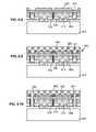
- FIGS. 5 . 1 - 5 . 11show a fabrication process for making a cMUT of the present invention using wafer bonding process. The steps of the process are described below.
- step one( FIG. 5.1 ) a desired recess pattern is formed on substrate 501 .
- step twothe substrate 501 is further patterned to a desired thickness pattern to define anchors 510 and posts 515 .
- the anchors 510will become a part of the lower portion of the base to support the spring layer to be formed.
- the optional posts 515will serve as motion stoppers.
- step threeAn SOI wafer including the desired spring layer 520 is bounded on the substrate 501 .
- the handle wafer and the box of the SOI waferare subsequently removed to form the spring layer 520 .
- a prime wafermay be used to introduce the spring layer 520 .
- step fourthe spring layer 520 is patterned in preparation for forming or connecting the spring-played connectors and the upper portion of the base in the next steps.
- a prime layer 560is bonded to the spring layer 520 , and is ground and polished to a desired thickness to form the upper portion ( 560 ) of the cMUT base.
- an SOI wafermay be used at this step to replace the prime wafer.
- a separate conductive layermay be deposited to form a bottom electrode in this step if needed.
- step six( FIG. 5.6 ), a dielectric layer 562 is deposited and patterned to partially form the spring-plate connectors to support the top plate to be introduced.
- step sevenan insulation layer 564 is grown and patterned.
- the optional insulation layer 564becomes the top of the upper portion of the cMUT base.
- the dielectric layer 562 and the insulation layer 564have different heights, with the former being taller to support the top plate to be introduced and to define a gap between the top plate and the insulation layer 564 .
- step eightthe layer 560 is patterned to form the upper portions 560 .
- Trench openingsare formed through the layer 560 . This also forms the spring-plate connectors 530 passing through the trench openings.
- step nine( FIG. 5.9 ), a prime wafer 540 is bonded over the spring-plate connectors 530 , and ground and polished to form a top plate ( 540 ).
- an SOI wafermay be used in this step to replace the prime wafer.
- step ten( FIG. 5.10 ), a metal layer 550 is deposited and patterned to form the top electrode.
- step eleventrenches 555 are etched between the cMUT evidence to separate the individual cMUT elements.
- FIGS. 6 . 1 - 6 . 10show a fabrication process for making a cMUT of the present invention using sacrificial technology. The steps of the process are described below.
- step one( FIG. 6.1 ), a first sacrificial layer 681 is deposited and patterned on substrate 601 .
- step twoa material layer is deposited and patterned to form both the spring layer 620 and a part of the lower portion 610 of the cMUT base to support the spring layer 620 .
- Vias 621 for sacrificial layer removalare also formed through the spring layer 620 .
- the spring layer 620may appear to be disconnected from the lower portion 610 of the cMUT base, in 2-D or 3-D view these components are connected to form the cantilever-like spring structures of the present invention.
- a second sacrificial layer 682is deposited and patterned.
- the second sacrificial layer 682 and the first sacrificial layermay be designed to conduct to each other in order to facilitate easier sacrificial removal.
- step four( FIG. 6.4 ), layer 660 is deposited to form the upper portion of the cMUT base. If the layer 660 is made of the conductive material, this also forms the bottom electrode. Ultimately, a separate conductive layer may be deposited to form a bottom electrode in this step.
- step five( FIG. 6.5 ) a third sacrificial layer 683 is deposited and patterned to partially define the suppression gap between the bottom electrode and the top electrode to be formed.
- step six( FIG. 6.6 ), a thin-film layer 641 is deposited to form a part of the top plate 640 (to be completed) of the cMUT. Vias (not shown) may also be formed in this step to access the sacrificial layers.
- step seven( FIG. 6.7 ), sacrificial materials ( 681 , 682 and 683 ) are removed.
- the viasmay be sealed subsequently by spinning or depositing another thin-film layer.
- step eight( FIG. 6.8 ), a thin conductive layer 650 is deposited over the thin-film layer 641 to form the top electrode.
- a material layer 642is deposited to a desired thickness to complete the top plate 640 of the cMUT.
- the top plate 640comprises the thin-film layer 640 , the thing conductive layer 650 and the material layer 642 .
- the top electrode ( 650 )is embedded within the top plate ( 640 ).
- Other type of configurationsincluding using a conductive material for the entire top plate or depositing the conductive layer on top of the top plate, may also be used.
- step tentrenches 655 are etched between the cMUT evidence to separate the individual cMUT elements.
- FIGS. 7 . 1 - 7 . 7show a fabrication process for making another cMUT of the present invention. The steps of the process are described below.
- step one( FIG. 7.1 ), a first thermal oxide layer 702 is grown and patterned on substrate 701 .
- step twoa second thermal oxide layer 722 is deposited and patterned to form an insulation layer.
- the first thermal oxide layer 702is patterned to form a part of the vertical spring 720 .
- step threethe substrate 701 is etched to form deep trenches 725 and a complete vertical springs 720 therein.
- step four( FIG. 7.4 ), a prime wafer 740 is bonded over the vertical springs 720 to form the top plate 740 .
- step five( FIG. 7.5 ), a metal layer 750 is deposited and patterned to form the top electrode.
- step sixtrenches 755 are etched between the cMUT evidence to separate the individual cMUT elements.
- micro-electro-mechanical transducer in accordance with the present inventionhas been described in detail along with the figures and exemplary embodiments.
- the design of the micro-electro-mechanical transducer of the present inventionis particularly suitable for applications in capacitive micromachined ultrasonic transducers (cMUT), but can also be used in other micro-electro-mechanical devices which have a movable mechanical part to transform energy.
- cMUTcapacitive micromachined ultrasonic transducers
- micro-electro-mechanical transducer in accordance with the present inventionmay be fabricated using the fabrication methods or incorporated in the micro-electro-mechanical transducer as disclosed in international patent applications (PCT) No. PCT/IB2006/051566, entitled THROUGH-WAFER INTERCONNECTION, filed on May 18, 2006; No. PCT/IB2006/051567, entitled METHODS FOR FABRICATING MICRO-ELECTRO-MECHANICAL DEVICES, filed on May 18, 2006; No. PCT/IB2006/051568, entitled MICRO-ELECTRO-MECHANICAL TRANSDUCERS, filed on May 18, 2006; No.
Landscapes
- Engineering & Computer Science (AREA)
- Physics & Mathematics (AREA)
- Acoustics & Sound (AREA)
- Manufacturing & Machinery (AREA)
- Chemical & Material Sciences (AREA)
- Analytical Chemistry (AREA)
- Life Sciences & Earth Sciences (AREA)
- Health & Medical Sciences (AREA)
- Microelectronics & Electronic Packaging (AREA)
- Biochemistry (AREA)
- General Health & Medical Sciences (AREA)
- General Physics & Mathematics (AREA)
- Immunology (AREA)
- Pathology (AREA)
- Mechanical Engineering (AREA)
- Micromachines (AREA)
- Transducers For Ultrasonic Waves (AREA)
- Measuring Fluid Pressure (AREA)
Abstract
Description
Claims (16)
Priority Applications (1)
| Application Number | Priority Date | Filing Date | Title |
|---|---|---|---|
| US11/462,338US7564172B1 (en) | 2005-08-03 | 2006-08-03 | Micro-electro-mechanical transducer having embedded springs |
Applications Claiming Priority (3)
| Application Number | Priority Date | Filing Date | Title |
|---|---|---|---|
| US70560605P | 2005-08-03 | 2005-08-03 | |
| US74424206P | 2006-04-04 | 2006-04-04 | |
| US11/462,338US7564172B1 (en) | 2005-08-03 | 2006-08-03 | Micro-electro-mechanical transducer having embedded springs |
Publications (2)
| Publication Number | Publication Date |
|---|---|
| US20090167107A1 US20090167107A1 (en) | 2009-07-02 |
| US7564172B1true US7564172B1 (en) | 2009-07-21 |
Family
ID=37708995
Family Applications (2)
| Application Number | Title | Priority Date | Filing Date |
|---|---|---|---|
| US11/462,333Active2027-04-05US7612635B2 (en) | 2005-08-03 | 2006-08-03 | MEMS acoustic filter and fabrication of the same |
| US11/462,338ActiveUS7564172B1 (en) | 2005-08-03 | 2006-08-03 | Micro-electro-mechanical transducer having embedded springs |
Family Applications Before (1)
| Application Number | Title | Priority Date | Filing Date |
|---|---|---|---|
| US11/462,333Active2027-04-05US7612635B2 (en) | 2005-08-03 | 2006-08-03 | MEMS acoustic filter and fabrication of the same |
Country Status (2)
| Country | Link |
|---|---|
| US (2) | US7612635B2 (en) |
| WO (2) | WO2007015219A2 (en) |
Cited By (28)
| Publication number | Priority date | Publication date | Assignee | Title |
|---|---|---|---|---|
| US20080194053A1 (en)* | 2005-05-18 | 2008-08-14 | Kolo Technologies, Inc. | Methods for Fabricating Micro-Electro-Mechanical Devices |
| US20080203556A1 (en)* | 2005-05-18 | 2008-08-28 | Kolo Technologies, Inc. | Through-Wafer Interconnection |
| US20080290756A1 (en)* | 2005-06-17 | 2008-11-27 | Kolo Technologies, Inc. | Micro-Electro-Mechanical Transducer Having an Insulation Extension |
| US20090152980A1 (en)* | 2006-04-04 | 2009-06-18 | Kolo Technologies, Inc. | Electrostatic Comb Driver Actuator/Transducer and Fabrication of the Same |
| US8324006B1 (en)* | 2009-10-28 | 2012-12-04 | National Semiconductor Corporation | Method of forming a capacitive micromachined ultrasonic transducer (CMUT) |
| US8563345B2 (en) | 2009-10-02 | 2013-10-22 | National Semiconductor Corporated | Integration of structurally-stable isolated capacitive micromachined ultrasonic transducer (CMUT) array cells and array elements |
| US9061318B2 (en) | 2013-03-15 | 2015-06-23 | Butterfly Network, Inc. | Complementary metal oxide semiconductor (CMOS) ultrasonic transducers and methods for forming the same |
| US9067779B1 (en) | 2014-07-14 | 2015-06-30 | Butterfly Network, Inc. | Microfabricated ultrasonic transducers and related apparatus and methods |
| US20150369907A1 (en)* | 2014-06-23 | 2015-12-24 | Goodrich Corporation | Systems and methods for acoustic windows |
| US9221077B2 (en) | 2012-05-09 | 2015-12-29 | Kolo Technologies, Inc. | CMUT assembly with acoustic window |
| US9229097B2 (en) | 2014-04-18 | 2016-01-05 | Butterfly Network, Inc. | Architecture of single substrate ultrasonic imaging devices, related apparatuses, and methods |
| US9327142B2 (en) | 2013-03-15 | 2016-05-03 | Butterfly Network, Inc. | Monolithic ultrasonic imaging devices, systems and methods |
| US9351706B2 (en) | 2013-07-23 | 2016-05-31 | Butterfly Network, Inc. | Interconnectable ultrasound transducer probes and related methods and apparatus |
| US9499392B2 (en) | 2013-02-05 | 2016-11-22 | Butterfly Network, Inc. | CMOS ultrasonic transducers and related apparatus and methods |
| US9505030B2 (en) | 2014-04-18 | 2016-11-29 | Butterfly Network, Inc. | Ultrasonic transducers in complementary metal oxide semiconductor (CMOS) wafers and related apparatus and methods |
| US9592032B2 (en) | 2014-04-18 | 2017-03-14 | Butterfly Network, Inc. | Ultrasonic imaging compression methods and apparatus |
| US9667889B2 (en) | 2013-04-03 | 2017-05-30 | Butterfly Network, Inc. | Portable electronic devices with integrated imaging capabilities |
| US9987661B2 (en) | 2015-12-02 | 2018-06-05 | Butterfly Network, Inc. | Biasing of capacitive micromachined ultrasonic transducers (CMUTs) and related apparatus and methods |
| US10011476B1 (en) | 2016-12-29 | 2018-07-03 | Industrial Technology Research Institute | MEMS apparatus having impact absorber |
| US10084394B2 (en)* | 2009-12-11 | 2018-09-25 | Canon Kabushiki Kaisha | Control apparatus for capacitive electromechanical transducer, and method of controlling the capacitive electromechanical transducer |
| US10196261B2 (en) | 2017-03-08 | 2019-02-05 | Butterfly Network, Inc. | Microfabricated ultrasonic transducers and related apparatus and methods |
| US10399121B2 (en) | 2016-09-12 | 2019-09-03 | Kolo Medical, Ltd. | Bias application for capacitive micromachined ultrasonic transducers |
| US10413938B2 (en) | 2015-11-18 | 2019-09-17 | Kolo Medical, Ltd. | Capacitive micromachined ultrasound transducers having varying properties |
| US10512936B2 (en) | 2017-06-21 | 2019-12-24 | Butterfly Network, Inc. | Microfabricated ultrasonic transducer having individual cells with electrically isolated electrode sections |
| US10613058B2 (en) | 2017-06-27 | 2020-04-07 | Kolo Medical, Ltd. | CMUT signal separation with multi-level bias control |
| US10618078B2 (en) | 2016-07-18 | 2020-04-14 | Kolo Medical, Ltd. | Bias control for capacitive micromachined ultrasonic transducers |
| US11173520B2 (en) | 2020-01-20 | 2021-11-16 | The Board Of Trustees Of The Leland Stanford Junior University | Pulse train excitation for capacative micromachined ultrasonic transducer |
| US11738369B2 (en) | 2020-02-17 | 2023-08-29 | GE Precision Healthcare LLC | Capactive micromachined transducer having a high contact resistance part |
Families Citing this family (66)
| Publication number | Priority date | Publication date | Assignee | Title |
|---|---|---|---|---|
| US20090082673A1 (en)* | 2007-09-26 | 2009-03-26 | Xuanming Lu | Semiconductor matching layer in a layered ultrasound transducer array |
| US7843022B2 (en)* | 2007-10-18 | 2010-11-30 | The Board Of Trustees Of The Leland Stanford Junior University | High-temperature electrostatic transducers and fabrication method |
| JP5337813B2 (en)* | 2007-12-03 | 2013-11-06 | コロ テクノロジーズ インコーポレイテッド | Dual-mode operation micromachined ultrasonic transducer |
| FR2939003B1 (en)* | 2008-11-21 | 2011-02-25 | Commissariat Energie Atomique | CMUT CELL FORMED OF A MEMBRANE OF NANO-TUBES OR NANO-THREADS OR NANO-BEAMS AND ULTRA HIGH-FREQUENCY ACOUSTIC IMAGING DEVICE COMPRISING A PLURALITY OF SUCH CELLS |
| WO2010148398A2 (en)* | 2009-06-19 | 2010-12-23 | The Regents Of The University Of Michigan | A thin-film device and method of fabricating the same |
| JP5578810B2 (en) | 2009-06-19 | 2014-08-27 | キヤノン株式会社 | Capacitance type electromechanical transducer |
| US9327316B2 (en)* | 2009-06-30 | 2016-05-03 | Avago Technologies General Ip (Singapore) Pte. Ltd. | Multi-frequency acoustic array |
| US8451693B2 (en)* | 2009-08-25 | 2013-05-28 | The Board Of Trustees Of The Leland Stanford Junior University | Micromachined ultrasonic transducer having compliant post structure |
| JP5402823B2 (en)* | 2010-05-13 | 2014-01-29 | オムロン株式会社 | Acoustic sensor |
| EP2506430B1 (en) | 2011-03-28 | 2017-11-22 | Nxp B.V. | Resonator and method of controlling the same |
| KR101813183B1 (en)* | 2011-12-19 | 2017-12-29 | 삼성전자주식회사 | cell, element of ultrasonic transducer, ultrasonic transducer including the sames, and method of manufacturing the sames |
| JP2013156066A (en)* | 2012-01-27 | 2013-08-15 | Wacom Co Ltd | Electrical capacitance pressure sensing semiconductor device |
| JP5892595B2 (en) | 2012-02-06 | 2016-03-23 | 株式会社ワコム | Position indicator |
| US8964898B2 (en)* | 2012-09-14 | 2015-02-24 | Northrop Grumman Systems Corporation | Multi-function receiver with switched channelizer having high dynamic range active microwave filters using carbon nanotube electronics |
| JP5835285B2 (en) | 2013-07-24 | 2015-12-24 | 横河電機株式会社 | Vibrating transducer and manufacturing method thereof |
| JP2015023994A (en)* | 2013-07-26 | 2015-02-05 | セイコーエプソン株式会社 | Ultrasonic measurement device, ultrasonic head unit, ultrasonic probe, and ultrasonic imaging device |
| JP5807664B2 (en) | 2013-08-07 | 2015-11-10 | 横河電機株式会社 | Vibrating transducer and manufacturing method thereof |
| US20200322731A1 (en)* | 2013-10-17 | 2020-10-08 | Merry Electronics(Shenzhen) Co., Ltd. | Acoustic transducer |
| EP2977113A1 (en)* | 2014-07-24 | 2016-01-27 | Koninklijke Philips N.V. | CMUT ultrasound focusing by means of partially removed curved substrate |
| US11084062B2 (en)* | 2015-11-02 | 2021-08-10 | Koninklijke Philips N.V. | Ultrasound transducer array, probe and system |
| US10670716B2 (en) | 2016-05-04 | 2020-06-02 | Invensense, Inc. | Operating a two-dimensional array of ultrasonic transducers |
| US10445547B2 (en) | 2016-05-04 | 2019-10-15 | Invensense, Inc. | Device mountable packaging of ultrasonic transducers |
| US10656255B2 (en) | 2016-05-04 | 2020-05-19 | Invensense, Inc. | Piezoelectric micromachined ultrasonic transducer (PMUT) |
| US10325915B2 (en) | 2016-05-04 | 2019-06-18 | Invensense, Inc. | Two-dimensional array of CMOS control elements |
| US10315222B2 (en) | 2016-05-04 | 2019-06-11 | Invensense, Inc. | Two-dimensional array of CMOS control elements |
| US10600403B2 (en) | 2016-05-10 | 2020-03-24 | Invensense, Inc. | Transmit operation of an ultrasonic sensor |
| US10632500B2 (en) | 2016-05-10 | 2020-04-28 | Invensense, Inc. | Ultrasonic transducer with a non-uniform membrane |
| US10441975B2 (en) | 2016-05-10 | 2019-10-15 | Invensense, Inc. | Supplemental sensor modes and systems for ultrasonic transducers |
| US10452887B2 (en) | 2016-05-10 | 2019-10-22 | Invensense, Inc. | Operating a fingerprint sensor comprised of ultrasonic transducers |
| US10539539B2 (en) | 2016-05-10 | 2020-01-21 | Invensense, Inc. | Operation of an ultrasonic sensor |
| US11673165B2 (en) | 2016-05-10 | 2023-06-13 | Invensense, Inc. | Ultrasonic transducer operable in a surface acoustic wave (SAW) mode |
| US10706835B2 (en) | 2016-05-10 | 2020-07-07 | Invensense, Inc. | Transmit beamforming of a two-dimensional array of ultrasonic transducers |
| US10562070B2 (en) | 2016-05-10 | 2020-02-18 | Invensense, Inc. | Receive operation of an ultrasonic sensor |
| US10408797B2 (en) | 2016-05-10 | 2019-09-10 | Invensense, Inc. | Sensing device with a temperature sensor |
| WO2018035486A1 (en)* | 2016-08-18 | 2018-02-22 | Vesper Technologies Inc. | Plate coupling structure |
| KR101807146B1 (en)* | 2016-09-09 | 2017-12-07 | 현대자동차 주식회사 | High sensitivity microphone and manufacturing method thereof |
| US10167191B2 (en)* | 2017-04-04 | 2019-01-01 | Kionix, Inc. | Method for manufacturing a micro electro-mechanical system |
| US10891461B2 (en) | 2017-05-22 | 2021-01-12 | Invensense, Inc. | Live fingerprint detection utilizing an integrated ultrasound and infrared sensor |
| US10474862B2 (en)* | 2017-06-01 | 2019-11-12 | Invensense, Inc. | Image generation in an electronic device using ultrasonic transducers |
| US10643052B2 (en) | 2017-06-28 | 2020-05-05 | Invensense, Inc. | Image generation in an electronic device using ultrasonic transducers |
| US10997388B2 (en) | 2017-12-01 | 2021-05-04 | Invensense, Inc. | Darkfield contamination detection |
| US10936841B2 (en) | 2017-12-01 | 2021-03-02 | Invensense, Inc. | Darkfield tracking |
| US10984209B2 (en) | 2017-12-01 | 2021-04-20 | Invensense, Inc. | Darkfield modeling |
| US11151355B2 (en) | 2018-01-24 | 2021-10-19 | Invensense, Inc. | Generation of an estimated fingerprint |
| US10755067B2 (en) | 2018-03-22 | 2020-08-25 | Invensense, Inc. | Operating a fingerprint sensor comprised of ultrasonic transducers |
| CN110147050B (en)* | 2018-06-06 | 2021-07-06 | 北京纳米能源与系统研究所 | a monitoring system |
| US10936843B2 (en) | 2018-12-28 | 2021-03-02 | Invensense, Inc. | Segmented image acquisition |
| US11188735B2 (en) | 2019-06-24 | 2021-11-30 | Invensense, Inc. | Fake finger detection using ridge features |
| US11216681B2 (en) | 2019-06-25 | 2022-01-04 | Invensense, Inc. | Fake finger detection based on transient features |
| US11176345B2 (en) | 2019-07-17 | 2021-11-16 | Invensense, Inc. | Ultrasonic fingerprint sensor with a contact layer of non-uniform thickness |
| US11216632B2 (en) | 2019-07-17 | 2022-01-04 | Invensense, Inc. | Ultrasonic fingerprint sensor with a contact layer of non-uniform thickness |
| EP4003611A1 (en) | 2019-07-26 | 2022-06-01 | Vermon S.A. | Cmut transducer and method for manufacturing |
| US11232549B2 (en) | 2019-08-23 | 2022-01-25 | Invensense, Inc. | Adapting a quality threshold for a fingerprint image |
| EP4021648A1 (en)* | 2019-08-30 | 2022-07-06 | Vermon S.A. | Cmut transducer with motion-stopping structure and cmut transducer forming method |
| US11392789B2 (en) | 2019-10-21 | 2022-07-19 | Invensense, Inc. | Fingerprint authentication using a synthetic enrollment image |
| US11460957B2 (en) | 2020-03-09 | 2022-10-04 | Invensense, Inc. | Ultrasonic fingerprint sensor with a contact layer of non-uniform thickness |
| US11243300B2 (en) | 2020-03-10 | 2022-02-08 | Invensense, Inc. | Operating a fingerprint sensor comprised of ultrasonic transducers and a presence sensor |
| US11328165B2 (en) | 2020-04-24 | 2022-05-10 | Invensense, Inc. | Pressure-based activation of fingerprint spoof detection |
| US11995909B2 (en) | 2020-07-17 | 2024-05-28 | Tdk Corporation | Multipath reflection correction |
| US12174295B2 (en) | 2020-08-07 | 2024-12-24 | Tdk Corporation | Acoustic multipath correction |
| CN112261563A (en)* | 2020-10-22 | 2021-01-22 | 常州元晶电子科技有限公司 | Mems digital loudspeaker system and working method thereof |
| US11911792B2 (en)* | 2021-01-12 | 2024-02-27 | GE Precision Healthcare LLC | Micromachined ultrasonic transources with dual out-of-plane and in-plane actuation and displacement |
| CN112765849B (en)* | 2021-01-15 | 2023-07-11 | 北京航天微电科技有限公司 | Method and device for determining thickness of insulating layer of filter |
| US12416807B2 (en) | 2021-08-20 | 2025-09-16 | Tdk Corporation | Retinal projection display system |
| US12260050B2 (en) | 2021-08-25 | 2025-03-25 | Tdk Corporation | Differential receive at an ultrasonic transducer |
| EP4197965A1 (en)* | 2021-12-16 | 2023-06-21 | Murata Manufacturing Co., Ltd. | Method for structural layer fabrication in micromechanical devices |
Citations (7)
| Publication number | Priority date | Publication date | Assignee | Title |
|---|---|---|---|---|
| US4183126A (en)* | 1976-09-09 | 1980-01-15 | Kabushiki Kaisha Seikosha | Process for preparing quartz oscillator |
| US5142307A (en)* | 1990-12-26 | 1992-08-25 | Xerox Corporation | Variable orifice capillary wave printer |
| US5597358A (en)* | 1994-05-25 | 1997-01-28 | Marcu; Mihail I. | Free fall system |
| US5917272A (en)* | 1998-06-11 | 1999-06-29 | Vectron, Inc. | Oven-heated crystal resonator and oscillator assembly |
| US20040145277A1 (en)* | 2000-07-11 | 2004-07-29 | Robert Horning | MEMS actuator with lower power consumption and lower cost simplified fabrication |
| US6812055B2 (en)* | 2002-02-21 | 2004-11-02 | Advanced Microsensors | MEMS devices and methods of manufacture |
| US6917086B2 (en)* | 2001-11-09 | 2005-07-12 | Turnstone Systems, Inc. | Trilayered beam MEMS device and related methods |
Family Cites Families (20)
| Publication number | Priority date | Publication date | Assignee | Title |
|---|---|---|---|---|
| US5578976A (en)* | 1995-06-22 | 1996-11-26 | Rockwell International Corporation | Micro electromechanical RF switch |
| US6593831B2 (en)* | 1999-01-14 | 2003-07-15 | The Regents Of The University Of Michigan | Method and apparatus for filtering signals in a subsystem including a power amplifier utilizing a bank of vibrating micromechanical apparatus |
| US6271620B1 (en)* | 1999-05-20 | 2001-08-07 | Sen Corporation | Acoustic transducer and method of making the same |
| US6384353B1 (en)* | 2000-02-01 | 2002-05-07 | Motorola, Inc. | Micro-electromechanical system device |
| US6424165B1 (en)* | 2000-09-20 | 2002-07-23 | Sandia Corporation | Electrostatic apparatus for measurement of microfracture strength |
| US6473361B1 (en)* | 2000-11-10 | 2002-10-29 | Xerox Corporation | Electromechanical memory cell |
| US6508947B2 (en)* | 2001-01-24 | 2003-01-21 | Xerox Corporation | Method for fabricating a micro-electro-mechanical fluid ejector |
| KR100738064B1 (en)* | 2001-02-27 | 2007-07-12 | 삼성전자주식회사 | MEMS element with spring of nonlinear restoring force |
| US6503847B2 (en)* | 2001-04-26 | 2003-01-07 | Institute Of Microelectronics | Room temperature wafer-to-wafer bonding by polydimethylsiloxane |
| US6700688B2 (en)* | 2001-08-24 | 2004-03-02 | Megasense, Inc. | Rolling mirror apparatus and method of use |
| US7309620B2 (en)* | 2002-01-11 | 2007-12-18 | The Penn State Research Foundation | Use of sacrificial layers in the manufacture of high performance systems on tailored substrates |
| JP4186727B2 (en)* | 2002-07-26 | 2008-11-26 | 松下電器産業株式会社 | switch |
| US7047810B2 (en)* | 2003-01-15 | 2006-05-23 | Ahura Corporation | Micro-electro-mechanical pressure sensor |
| JP2005092174A (en)* | 2003-08-12 | 2005-04-07 | Fujitsu Ltd | Micro oscillating device |
| US20050067919A1 (en)* | 2003-09-30 | 2005-03-31 | Horning Robert D. | Polymer actuator having a circular unit cell |
| US7265477B2 (en)* | 2004-01-05 | 2007-09-04 | Chang-Feng Wan | Stepping actuator and method of manufacture therefore |
| US7118991B2 (en)* | 2004-04-01 | 2006-10-10 | Delphi Technologies, Inc. | Encapsulation wafer process |
| US6956389B1 (en)* | 2004-08-16 | 2005-10-18 | Jem America Corporation | Highly resilient cantilever spring probe for testing ICs |
| US7321185B2 (en)* | 2005-03-04 | 2008-01-22 | United States Of America As Represented By The Administrator Of The National Aeronautics And Space Administration | Active multistable twisting device |
| KR100693345B1 (en)* | 2005-11-30 | 2007-03-09 | 삼성전자주식회사 | MEMS switch |
- 2006
- 2006-08-03USUS11/462,333patent/US7612635B2/enactiveActive
- 2006-08-03WOPCT/IB2006/052658patent/WO2007015219A2/enactiveApplication Filing
- 2006-08-03WOPCT/IB2006/052657patent/WO2007015218A2/enactiveApplication Filing
- 2006-08-03USUS11/462,338patent/US7564172B1/enactiveActive
Patent Citations (7)
| Publication number | Priority date | Publication date | Assignee | Title |
|---|---|---|---|---|
| US4183126A (en)* | 1976-09-09 | 1980-01-15 | Kabushiki Kaisha Seikosha | Process for preparing quartz oscillator |
| US5142307A (en)* | 1990-12-26 | 1992-08-25 | Xerox Corporation | Variable orifice capillary wave printer |
| US5597358A (en)* | 1994-05-25 | 1997-01-28 | Marcu; Mihail I. | Free fall system |
| US5917272A (en)* | 1998-06-11 | 1999-06-29 | Vectron, Inc. | Oven-heated crystal resonator and oscillator assembly |
| US20040145277A1 (en)* | 2000-07-11 | 2004-07-29 | Robert Horning | MEMS actuator with lower power consumption and lower cost simplified fabrication |
| US6917086B2 (en)* | 2001-11-09 | 2005-07-12 | Turnstone Systems, Inc. | Trilayered beam MEMS device and related methods |
| US6812055B2 (en)* | 2002-02-21 | 2004-11-02 | Advanced Microsensors | MEMS devices and methods of manufacture |
Cited By (88)
| Publication number | Priority date | Publication date | Assignee | Title |
|---|---|---|---|---|
| US20080197751A1 (en)* | 2005-05-18 | 2008-08-21 | Kolo Technologies, Inc. | Micro-Electro-Mechanical Transducers |
| US20080203556A1 (en)* | 2005-05-18 | 2008-08-28 | Kolo Technologies, Inc. | Through-Wafer Interconnection |
| US20090140606A1 (en)* | 2005-05-18 | 2009-06-04 | Kolo Technologies, Inc. | Micro-Electro-Mechanical Transducers |
| US9224648B2 (en) | 2005-05-18 | 2015-12-29 | Kolo Technologies, Inc. | Through-wafer interconnection |
| US8008105B2 (en)* | 2005-05-18 | 2011-08-30 | Kolo Technologies, Inc. | Methods for fabricating micro-electro-mechanical devices |
| US8105941B2 (en) | 2005-05-18 | 2012-01-31 | Kolo Technologies, Inc. | Through-wafer interconnection |
| US8120229B2 (en)* | 2005-05-18 | 2012-02-21 | Kolo Technologies, Inc. | Middle spring supported micro-electro-mechanical transducers |
| US8247945B2 (en) | 2005-05-18 | 2012-08-21 | Kolo Technologies, Inc. | Micro-electro-mechanical transducers |
| US20080194053A1 (en)* | 2005-05-18 | 2008-08-14 | Kolo Technologies, Inc. | Methods for Fabricating Micro-Electro-Mechanical Devices |
| US8952595B2 (en) | 2005-05-18 | 2015-02-10 | Kolo Technologies, Inc. | Micro-electro-mechanical transducers |
| US8796901B2 (en) | 2005-06-17 | 2014-08-05 | Kolo Technologies, Inc. | Micro-electro-mechanical transducer having an insulation extension |
| US20080290756A1 (en)* | 2005-06-17 | 2008-11-27 | Kolo Technologies, Inc. | Micro-Electro-Mechanical Transducer Having an Insulation Extension |
| US20090152980A1 (en)* | 2006-04-04 | 2009-06-18 | Kolo Technologies, Inc. | Electrostatic Comb Driver Actuator/Transducer and Fabrication of the Same |
| US9132450B2 (en)* | 2006-04-04 | 2015-09-15 | Kolo Technologies, Inc. | Electrostatic comb driver actuator/transducer and fabrication of the same |
| US8563345B2 (en) | 2009-10-02 | 2013-10-22 | National Semiconductor Corporated | Integration of structurally-stable isolated capacitive micromachined ultrasonic transducer (CMUT) array cells and array elements |
| US8324006B1 (en)* | 2009-10-28 | 2012-12-04 | National Semiconductor Corporation | Method of forming a capacitive micromachined ultrasonic transducer (CMUT) |
| US10084394B2 (en)* | 2009-12-11 | 2018-09-25 | Canon Kabushiki Kaisha | Control apparatus for capacitive electromechanical transducer, and method of controlling the capacitive electromechanical transducer |
| US9662679B2 (en) | 2012-05-09 | 2017-05-30 | Kolo Technologies, Inc. | CMUT assembly with acoustic window |
| US9975146B2 (en) | 2012-05-09 | 2018-05-22 | Kolo Technologies, Inc. | CMUT assembly with acoustic window |
| US9221077B2 (en) | 2012-05-09 | 2015-12-29 | Kolo Technologies, Inc. | CMUT assembly with acoustic window |
| US11833542B2 (en) | 2013-02-05 | 2023-12-05 | Bfly Operations, Inc. | CMOS ultrasonic transducers and related apparatus and methods |
| US10272470B2 (en) | 2013-02-05 | 2019-04-30 | Butterfly Network, Inc. | CMOS ultrasonic transducers and related apparatus and methods |
| US10518292B2 (en) | 2013-02-05 | 2019-12-31 | Butterfly Network, Inc. | CMOS ultrasonic transducers and related apparatus and methods |
| US10843227B2 (en) | 2013-02-05 | 2020-11-24 | Butterfly Network, Inc. | CMOS ultrasonic transducers and related apparatus and methods |
| US11684949B2 (en) | 2013-02-05 | 2023-06-27 | Bfly Operations, Inc. | CMOS ultrasonic transducers and related apparatus and methods |
| US9895718B2 (en) | 2013-02-05 | 2018-02-20 | Butterfly Network, Inc. | CMOS ultrasonic transducers and related apparatus and methods |
| US9718098B2 (en) | 2013-02-05 | 2017-08-01 | Butterfly Network, Inc. | CMOS ultrasonic transducers and related apparatus and methods |
| US9499392B2 (en) | 2013-02-05 | 2016-11-22 | Butterfly Network, Inc. | CMOS ultrasonic transducers and related apparatus and methods |
| US9533873B2 (en) | 2013-02-05 | 2017-01-03 | Butterfly Network, Inc. | CMOS ultrasonic transducers and related apparatus and methods |
| US9944514B2 (en) | 2013-03-15 | 2018-04-17 | Butterfly Network, Inc. | Complementary metal oxide semiconductor (CMOS) ultrasonic transducers and methods for forming the same |
| US9327142B2 (en) | 2013-03-15 | 2016-05-03 | Butterfly Network, Inc. | Monolithic ultrasonic imaging devices, systems and methods |
| US9521991B2 (en) | 2013-03-15 | 2016-12-20 | Butterfly Network, Inc. | Monolithic ultrasonic imaging devices, systems and methods |
| US9499395B2 (en) | 2013-03-15 | 2016-11-22 | Butterfly Network, Inc. | Complementary metal oxide semiconductor (CMOS) ultrasonic transducers and methods for forming the same |
| US9061318B2 (en) | 2013-03-15 | 2015-06-23 | Butterfly Network, Inc. | Complementary metal oxide semiconductor (CMOS) ultrasonic transducers and methods for forming the same |
| US11439364B2 (en) | 2013-03-15 | 2022-09-13 | Bfly Operations, Inc. | Ultrasonic imaging devices, systems and methods |
| US10856847B2 (en) | 2013-03-15 | 2020-12-08 | Butterfly Network, Inc. | Monolithic ultrasonic imaging devices, systems and methods |
| US10710873B2 (en) | 2013-03-15 | 2020-07-14 | Butterfly Network, Inc. | Complementary metal oxide semiconductor (CMOS) ultrasonic transducers and methods for forming the same |
| US9738514B2 (en) | 2013-03-15 | 2017-08-22 | Butterfly Network, Inc. | Complementary metal oxide semiconductor (CMOS) ultrasonic transducers and methods for forming the same |
| US9242275B2 (en) | 2013-03-15 | 2016-01-26 | Butterfly Networks, Inc. | Complementary metal oxide semiconductor (CMOS) ultrasonic transducers and methods for forming the same |
| US10266401B2 (en) | 2013-03-15 | 2019-04-23 | Butterfly Network, Inc. | Complementary metal oxide semiconductor (CMOS) ultrasonic transducers and methods for forming the same |
| US9290375B2 (en) | 2013-03-15 | 2016-03-22 | Butterfly Network, Inc. | Complementary metal oxide semiconductor (CMOS) ultrasonic transducers and methods for forming the same |
| US9667889B2 (en) | 2013-04-03 | 2017-05-30 | Butterfly Network, Inc. | Portable electronic devices with integrated imaging capabilities |
| US11039812B2 (en) | 2013-07-23 | 2021-06-22 | Butterfly Network, Inc. | Interconnectable ultrasound transducer probes and related methods and apparatus |
| US9351706B2 (en) | 2013-07-23 | 2016-05-31 | Butterfly Network, Inc. | Interconnectable ultrasound transducer probes and related methods and apparatus |
| US9592030B2 (en) | 2013-07-23 | 2017-03-14 | Butterfly Network, Inc. | Interconnectable ultrasound transducer probes and related methods and apparatus |
| US11647985B2 (en) | 2013-07-23 | 2023-05-16 | Bfly Operations, Inc. | Interconnectable ultrasound transducer probes and related methods and apparatus |
| US10980511B2 (en) | 2013-07-23 | 2021-04-20 | Butterfly Network, Inc. | Interconnectable ultrasound transducer probes and related methods and apparatus |
| US10707201B2 (en) | 2014-04-18 | 2020-07-07 | Butterfly Network, Inc. | Ultrasonic transducers in complementary metal oxide semiconductor (CMOS) wafers and related apparatus and methods |
| US9229097B2 (en) | 2014-04-18 | 2016-01-05 | Butterfly Network, Inc. | Architecture of single substrate ultrasonic imaging devices, related apparatuses, and methods |
| US12426857B2 (en) | 2014-04-18 | 2025-09-30 | Bfly Operations, Inc. | Ultrasonic imaging compression methods and apparatus |
| US11914079B2 (en)* | 2014-04-18 | 2024-02-27 | Bfly Operations, Inc. | Architecture of single substrate ultrasonic imaging devices, related apparatuses, and methods |
| US20230093524A1 (en)* | 2014-04-18 | 2023-03-23 | Bfly Operations, Inc. | Architecture of single substrate ultrasonic imaging devices, related apparatuses, and methods |
| US9592032B2 (en) | 2014-04-18 | 2017-03-14 | Butterfly Network, Inc. | Ultrasonic imaging compression methods and apparatus |
| US11435458B2 (en) | 2014-04-18 | 2022-09-06 | Bfly Operations, Inc. | Architecture of single substrate ultrasonic imaging devices, related apparatuses, and methods |
| US9899371B2 (en) | 2014-04-18 | 2018-02-20 | Butterfly Network, Inc. | Ultrasonic transducers in complementary metal oxide semiconductor (CMOS) wafers and related apparatus and methods |
| US9505030B2 (en) | 2014-04-18 | 2016-11-29 | Butterfly Network, Inc. | Ultrasonic transducers in complementary metal oxide semiconductor (CMOS) wafers and related apparatus and methods |
| US9476969B2 (en) | 2014-04-18 | 2016-10-25 | Butterfly Network, Inc. | Architecture of single substrate ultrasonic imaging devices, related apparatuses, and methods |
| US10416298B2 (en) | 2014-04-18 | 2019-09-17 | Butterfly Network, Inc. | Architecture of single substrate ultrasonic imaging devices, related apparatuses, and methods |
| US10177139B2 (en) | 2014-04-18 | 2019-01-08 | Butterfly Network, Inc. | Ultrasonic transducers in complementary metal oxide semiconductor (CMOS) wafers and related apparatus and methods |
| US20150369907A1 (en)* | 2014-06-23 | 2015-12-24 | Goodrich Corporation | Systems and methods for acoustic windows |
| US9411040B2 (en)* | 2014-06-23 | 2016-08-09 | Goodrich Corporation | Systems and methods for acoustic windows |
| US9394162B2 (en) | 2014-07-14 | 2016-07-19 | Butterfly Network, Inc. | Microfabricated ultrasonic transducers and related apparatus and methods |
| US11828729B2 (en) | 2014-07-14 | 2023-11-28 | Bfly Operations, Inc. | Microfabricated ultrasonic transducers and related apparatus and methods |
| US9910017B2 (en) | 2014-07-14 | 2018-03-06 | Butterfly Network, Inc. | Microfabricated ultrasonic transducers and related apparatus and methods |
| US9067779B1 (en) | 2014-07-14 | 2015-06-30 | Butterfly Network, Inc. | Microfabricated ultrasonic transducers and related apparatus and methods |
| US9910018B2 (en) | 2014-07-14 | 2018-03-06 | Butterfly Network, Inc. | Microfabricated ultrasonic transducers and related apparatus and methods |
| US10228353B2 (en) | 2014-07-14 | 2019-03-12 | Butterfly Networks, Inc. | Microfabricated ultrasonic transducers and related apparatus and methods |
| US10247708B2 (en) | 2014-07-14 | 2019-04-02 | Butterfly Network, Inc. | Microfabricated ultrasonic transducers and related apparatus and methods |
| US10782269B2 (en) | 2014-07-14 | 2020-09-22 | Butterfly Network, Inc. | Microfabricated ultrasonic transducers and related apparatus and methods |
| US10175206B2 (en) | 2014-07-14 | 2019-01-08 | Butterfly Network, Inc. | Microfabricated ultrasonic transducers and related apparatus and methods |
| US10413938B2 (en) | 2015-11-18 | 2019-09-17 | Kolo Medical, Ltd. | Capacitive micromachined ultrasound transducers having varying properties |
| US10272471B2 (en) | 2015-12-02 | 2019-04-30 | Butterfly Network, Inc. | Biasing of capacitive micromachined ultrasonic transducers (CMUTs) and related apparatus and methods |
| US9987661B2 (en) | 2015-12-02 | 2018-06-05 | Butterfly Network, Inc. | Biasing of capacitive micromachined ultrasonic transducers (CMUTs) and related apparatus and methods |
| US10618078B2 (en) | 2016-07-18 | 2020-04-14 | Kolo Medical, Ltd. | Bias control for capacitive micromachined ultrasonic transducers |
| US10399121B2 (en) | 2016-09-12 | 2019-09-03 | Kolo Medical, Ltd. | Bias application for capacitive micromachined ultrasonic transducers |
| US10011476B1 (en) | 2016-12-29 | 2018-07-03 | Industrial Technology Research Institute | MEMS apparatus having impact absorber |
| US10672974B2 (en) | 2017-03-08 | 2020-06-02 | Butterfly Network, Inc. | Microfabricated ultrasonic transducers and related apparatus and methods |
| US10196261B2 (en) | 2017-03-08 | 2019-02-05 | Butterfly Network, Inc. | Microfabricated ultrasonic transducers and related apparatus and methods |
| US10967400B2 (en) | 2017-06-21 | 2021-04-06 | Butterfly Network, Inc. | Microfabricated ultrasonic transducer having individual cells with electrically isolated electrode sections |
| US10512936B2 (en) | 2017-06-21 | 2019-12-24 | Butterfly Network, Inc. | Microfabricated ultrasonic transducer having individual cells with electrically isolated electrode sections |
| US11559827B2 (en) | 2017-06-21 | 2023-01-24 | Bfly Operations, Inc. | Microfabricated ultrasonic transducer having individual cells with electrically isolated electrode sections |
| US10525506B2 (en) | 2017-06-21 | 2020-01-07 | Butterfly Networks, Inc. | Microfabricated ultrasonic transducer having individual cells with electrically isolated electrode sections |
| US10613058B2 (en) | 2017-06-27 | 2020-04-07 | Kolo Medical, Ltd. | CMUT signal separation with multi-level bias control |
| US11260424B2 (en) | 2020-01-20 | 2022-03-01 | The Board Of Trustees Of The Leland Stanford Junior University | Contoured electrode for capacitive micromachined ultrasonic transducer |
| US11731164B2 (en) | 2020-01-20 | 2023-08-22 | The Board Of Trustees Of The Leland Stanford Junior University | Pulse train excitation for capacitive micromachined ultrasonic transducer |
| US12285780B2 (en) | 2020-01-20 | 2025-04-29 | The Board Of Trustees Of The Leland Stanford Junior University | Capacitive micromachined ultrasonic transducer with contoured electrode |
| US11173520B2 (en) | 2020-01-20 | 2021-11-16 | The Board Of Trustees Of The Leland Stanford Junior University | Pulse train excitation for capacative micromachined ultrasonic transducer |
| US11738369B2 (en) | 2020-02-17 | 2023-08-29 | GE Precision Healthcare LLC | Capactive micromachined transducer having a high contact resistance part |
Also Published As
| Publication number | Publication date |
|---|---|
| US7612635B2 (en) | 2009-11-03 |
| WO2007015219A2 (en) | 2007-02-08 |
| WO2007015218A2 (en) | 2007-02-08 |
| US20070046396A1 (en) | 2007-03-01 |
| WO2007015218A3 (en) | 2009-04-16 |
| WO2007015219A3 (en) | 2009-04-16 |
| US20090167107A1 (en) | 2009-07-02 |
Similar Documents
| Publication | Publication Date | Title |
|---|---|---|
| US7564172B1 (en) | Micro-electro-mechanical transducer having embedded springs | |
| US8120229B2 (en) | Middle spring supported micro-electro-mechanical transducers | |
| JP5128470B2 (en) | Microelectromechanical transducer with insulation extension | |
| US7880565B2 (en) | Micro-electro-mechanical transducer having a surface plate | |
| JP4869593B2 (en) | Micromachined ultrasonic transducer cell with compliant support structure | |
| US9132450B2 (en) | Electrostatic comb driver actuator/transducer and fabrication of the same | |
| US10661308B2 (en) | High displacement ultrasonic transducer | |
| US8483014B2 (en) | Micromachined ultrasonic transducers | |
| CN101578686B (en) | Method of manufacturing a microelectromechanical device |
Legal Events
| Date | Code | Title | Description |
|---|---|---|---|
| AS | Assignment | Owner name:KOLO TECHNOLOGIES, INC., CALIFORNIA Free format text:ASSIGNMENT OF ASSIGNORS INTEREST;ASSIGNOR:HUANG, YONGLI;REEL/FRAME:021772/0412 Effective date:20081101 | |
| STCF | Information on status: patent grant | Free format text:PATENTED CASE | |
| FPAY | Fee payment | Year of fee payment:4 | |
| FPAY | Fee payment | Year of fee payment:8 | |
| MAFP | Maintenance fee payment | Free format text:PAYMENT OF MAINTENANCE FEE, 12TH YR, SMALL ENTITY (ORIGINAL EVENT CODE: M2553); ENTITY STATUS OF PATENT OWNER: SMALL ENTITY Year of fee payment:12 | |
| AS | Assignment | Owner name:KOLO TECHNOLOGIES, INC., CALIFORNIA Free format text:CORRECTIVE ASSIGNMENT TO CORRECT THE STATE OF INCORPORATION PREVIOUSLY RECORDED AT REEL: 021772 FRAME: 0412. ASSIGNOR(S) HEREBY CONFIRMS THE ASSIGNMENT;ASSIGNOR:HUANG, YONGLI;REEL/FRAME:058725/0354 Effective date:20081101 | |
| AS | Assignment | Owner name:KOLO MEDICAL (SUZHOU) CO., LTD., CHINA Free format text:ASSIGNMENT OF ASSIGNORS INTEREST;ASSIGNOR:KOLO MEDICAL LTD.;REEL/FRAME:058791/0538 Effective date:20220116 Owner name:KOLO MEDICAL LTD., CALIFORNIA Free format text:ASSIGNMENT OF ASSIGNORS INTEREST;ASSIGNOR:KOLO TECHNOLOGIES, INC.;REEL/FRAME:058789/0549 Effective date:20220112 |