US7563659B2 - Method of fabricating poly-crystalline silicon thin film and method of fabricating transistor using the same - Google Patents
Method of fabricating poly-crystalline silicon thin film and method of fabricating transistor using the sameDownload PDFInfo
- Publication number
- US7563659B2 US7563659B2US11/003,326US332604AUS7563659B2US 7563659 B2US7563659 B2US 7563659B2US 332604 AUS332604 AUS 332604AUS 7563659 B2US7563659 B2US 7563659B2
- Authority
- US
- United States
- Prior art keywords
- poly
- thin film
- fabricating
- cvd
- icp
- Prior art date
- Legal status (The legal status is an assumption and is not a legal conclusion. Google has not performed a legal analysis and makes no representation as to the accuracy of the status listed.)
- Expired - Fee Related, expires
Links
Images


Classifications
- H—ELECTRICITY
- H10—SEMICONDUCTOR DEVICES; ELECTRIC SOLID-STATE DEVICES NOT OTHERWISE PROVIDED FOR
- H10D—INORGANIC ELECTRIC SEMICONDUCTOR DEVICES
- H10D30/00—Field-effect transistors [FET]
- H10D30/60—Insulated-gate field-effect transistors [IGFET]
- H10D30/67—Thin-film transistors [TFT]
- H—ELECTRICITY
- H01—ELECTRIC ELEMENTS
- H01L—SEMICONDUCTOR DEVICES NOT COVERED BY CLASS H10
- H01L21/00—Processes or apparatus adapted for the manufacture or treatment of semiconductor or solid state devices or of parts thereof
- H01L21/02—Manufacture or treatment of semiconductor devices or of parts thereof
- H01L21/02104—Forming layers
- H01L21/02107—Forming insulating materials on a substrate
- H01L21/02109—Forming insulating materials on a substrate characterised by the type of layer, e.g. type of material, porous/non-porous, pre-cursors, mixtures or laminates
- H01L21/02112—Forming insulating materials on a substrate characterised by the type of layer, e.g. type of material, porous/non-porous, pre-cursors, mixtures or laminates characterised by the material of the layer
- H01L21/02123—Forming insulating materials on a substrate characterised by the type of layer, e.g. type of material, porous/non-porous, pre-cursors, mixtures or laminates characterised by the material of the layer the material containing silicon
- H01L21/02164—Forming insulating materials on a substrate characterised by the type of layer, e.g. type of material, porous/non-porous, pre-cursors, mixtures or laminates characterised by the material of the layer the material containing silicon the material being a silicon oxide, e.g. SiO2
- H—ELECTRICITY
- H01—ELECTRIC ELEMENTS
- H01L—SEMICONDUCTOR DEVICES NOT COVERED BY CLASS H10
- H01L21/00—Processes or apparatus adapted for the manufacture or treatment of semiconductor or solid state devices or of parts thereof
- H01L21/02—Manufacture or treatment of semiconductor devices or of parts thereof
- H01L21/02104—Forming layers
- H01L21/02107—Forming insulating materials on a substrate
- H01L21/02225—Forming insulating materials on a substrate characterised by the process for the formation of the insulating layer
- H01L21/0226—Forming insulating materials on a substrate characterised by the process for the formation of the insulating layer formation by a deposition process
- H01L21/02263—Forming insulating materials on a substrate characterised by the process for the formation of the insulating layer formation by a deposition process deposition from the gas or vapour phase
- H01L21/02271—Forming insulating materials on a substrate characterised by the process for the formation of the insulating layer formation by a deposition process deposition from the gas or vapour phase deposition by decomposition or reaction of gaseous or vapour phase compounds, i.e. chemical vapour deposition
- H01L21/02274—Forming insulating materials on a substrate characterised by the process for the formation of the insulating layer formation by a deposition process deposition from the gas or vapour phase deposition by decomposition or reaction of gaseous or vapour phase compounds, i.e. chemical vapour deposition in the presence of a plasma [PECVD]
- H—ELECTRICITY
- H01—ELECTRIC ELEMENTS
- H01L—SEMICONDUCTOR DEVICES NOT COVERED BY CLASS H10
- H01L21/00—Processes or apparatus adapted for the manufacture or treatment of semiconductor or solid state devices or of parts thereof
- H01L21/02—Manufacture or treatment of semiconductor devices or of parts thereof
- H01L21/02104—Forming layers
- H01L21/02107—Forming insulating materials on a substrate
- H01L21/02296—Forming insulating materials on a substrate characterised by the treatment performed before or after the formation of the layer
- H01L21/02318—Forming insulating materials on a substrate characterised by the treatment performed before or after the formation of the layer post-treatment
- H01L21/02345—Forming insulating materials on a substrate characterised by the treatment performed before or after the formation of the layer post-treatment treatment by exposure to radiation, e.g. visible light
- H01L21/02354—Forming insulating materials on a substrate characterised by the treatment performed before or after the formation of the layer post-treatment treatment by exposure to radiation, e.g. visible light using a coherent radiation, e.g. a laser
- H—ELECTRICITY
- H01—ELECTRIC ELEMENTS
- H01L—SEMICONDUCTOR DEVICES NOT COVERED BY CLASS H10
- H01L21/00—Processes or apparatus adapted for the manufacture or treatment of semiconductor or solid state devices or of parts thereof
- H01L21/02—Manufacture or treatment of semiconductor devices or of parts thereof
- H01L21/02104—Forming layers
- H01L21/02365—Forming inorganic semiconducting materials on a substrate
- H01L21/02367—Substrates
- H01L21/0237—Materials
- H01L21/02422—Non-crystalline insulating materials, e.g. glass, polymers
- H—ELECTRICITY
- H01—ELECTRIC ELEMENTS
- H01L—SEMICONDUCTOR DEVICES NOT COVERED BY CLASS H10
- H01L21/00—Processes or apparatus adapted for the manufacture or treatment of semiconductor or solid state devices or of parts thereof
- H01L21/02—Manufacture or treatment of semiconductor devices or of parts thereof
- H01L21/02104—Forming layers
- H01L21/02365—Forming inorganic semiconducting materials on a substrate
- H01L21/02518—Deposited layers
- H01L21/02521—Materials
- H01L21/02524—Group 14 semiconducting materials
- H01L21/02532—Silicon, silicon germanium, germanium
- H—ELECTRICITY
- H01—ELECTRIC ELEMENTS
- H01L—SEMICONDUCTOR DEVICES NOT COVERED BY CLASS H10
- H01L21/00—Processes or apparatus adapted for the manufacture or treatment of semiconductor or solid state devices or of parts thereof
- H01L21/02—Manufacture or treatment of semiconductor devices or of parts thereof
- H01L21/02104—Forming layers
- H01L21/02365—Forming inorganic semiconducting materials on a substrate
- H01L21/02518—Deposited layers
- H01L21/02587—Structure
- H01L21/0259—Microstructure
- H01L21/02595—Microstructure polycrystalline
- H—ELECTRICITY
- H01—ELECTRIC ELEMENTS
- H01L—SEMICONDUCTOR DEVICES NOT COVERED BY CLASS H10
- H01L21/00—Processes or apparatus adapted for the manufacture or treatment of semiconductor or solid state devices or of parts thereof
- H01L21/02—Manufacture or treatment of semiconductor devices or of parts thereof
- H01L21/02104—Forming layers
- H01L21/02365—Forming inorganic semiconducting materials on a substrate
- H01L21/02612—Formation types
- H01L21/02617—Deposition types
- H01L21/0262—Reduction or decomposition of gaseous compounds, e.g. CVD
- H—ELECTRICITY
- H01—ELECTRIC ELEMENTS
- H01L—SEMICONDUCTOR DEVICES NOT COVERED BY CLASS H10
- H01L21/00—Processes or apparatus adapted for the manufacture or treatment of semiconductor or solid state devices or of parts thereof
- H01L21/02—Manufacture or treatment of semiconductor devices or of parts thereof
- H01L21/02104—Forming layers
- H01L21/02365—Forming inorganic semiconducting materials on a substrate
- H01L21/02656—Special treatments
- H01L21/02664—Aftertreatments
- H01L21/02667—Crystallisation or recrystallisation of non-monocrystalline semiconductor materials, e.g. regrowth
- H01L21/02675—Crystallisation or recrystallisation of non-monocrystalline semiconductor materials, e.g. regrowth using laser beams
- H01L21/02686—Pulsed laser beam
- H—ELECTRICITY
- H10—SEMICONDUCTOR DEVICES; ELECTRIC SOLID-STATE DEVICES NOT OTHERWISE PROVIDED FOR
- H10D—INORGANIC ELECTRIC SEMICONDUCTOR DEVICES
- H10D30/00—Field-effect transistors [FET]
- H10D30/01—Manufacture or treatment
- H10D30/021—Manufacture or treatment of FETs having insulated gates [IGFET]
- H10D30/031—Manufacture or treatment of FETs having insulated gates [IGFET] of thin-film transistors [TFT]
- H10D30/0312—Manufacture or treatment of FETs having insulated gates [IGFET] of thin-film transistors [TFT] characterised by the gate electrodes
- H10D30/0314—Manufacture or treatment of FETs having insulated gates [IGFET] of thin-film transistors [TFT] characterised by the gate electrodes of lateral top-gate TFTs comprising only a single gate
- H—ELECTRICITY
- H10—SEMICONDUCTOR DEVICES; ELECTRIC SOLID-STATE DEVICES NOT OTHERWISE PROVIDED FOR
- H10D—INORGANIC ELECTRIC SEMICONDUCTOR DEVICES
- H10D30/00—Field-effect transistors [FET]
- H10D30/01—Manufacture or treatment
- H10D30/021—Manufacture or treatment of FETs having insulated gates [IGFET]
- H10D30/031—Manufacture or treatment of FETs having insulated gates [IGFET] of thin-film transistors [TFT]
- H10D30/0321—Manufacture or treatment of FETs having insulated gates [IGFET] of thin-film transistors [TFT] comprising silicon, e.g. amorphous silicon or polysilicon
- H—ELECTRICITY
- H10—SEMICONDUCTOR DEVICES; ELECTRIC SOLID-STATE DEVICES NOT OTHERWISE PROVIDED FOR
- H10D—INORGANIC ELECTRIC SEMICONDUCTOR DEVICES
- H10D30/00—Field-effect transistors [FET]
- H10D30/60—Insulated-gate field-effect transistors [IGFET]
- H10D30/67—Thin-film transistors [TFT]
- H10D30/6729—Thin-film transistors [TFT] characterised by the electrodes
- H10D30/673—Thin-film transistors [TFT] characterised by the electrodes characterised by the shapes, relative sizes or dispositions of the gate electrodes
- H10D30/6731—Top-gate only TFTs
- H—ELECTRICITY
- H10—SEMICONDUCTOR DEVICES; ELECTRIC SOLID-STATE DEVICES NOT OTHERWISE PROVIDED FOR
- H10D—INORGANIC ELECTRIC SEMICONDUCTOR DEVICES
- H10D30/00—Field-effect transistors [FET]
- H10D30/60—Insulated-gate field-effect transistors [IGFET]
- H10D30/67—Thin-film transistors [TFT]
- H10D30/6729—Thin-film transistors [TFT] characterised by the electrodes
- H10D30/6737—Thin-film transistors [TFT] characterised by the electrodes characterised by the electrode materials
- H10D30/6739—Conductor-insulator-semiconductor electrodes
- H—ELECTRICITY
- H10—SEMICONDUCTOR DEVICES; ELECTRIC SOLID-STATE DEVICES NOT OTHERWISE PROVIDED FOR
- H10D—INORGANIC ELECTRIC SEMICONDUCTOR DEVICES
- H10D30/00—Field-effect transistors [FET]
- H10D30/60—Insulated-gate field-effect transistors [IGFET]
- H10D30/67—Thin-film transistors [TFT]
- H10D30/674—Thin-film transistors [TFT] characterised by the active materials
- H10D30/6741—Group IV materials, e.g. germanium or silicon carbide
- H10D30/6743—Silicon
- H10D30/6745—Polycrystalline or microcrystalline silicon
Definitions
- the present disclosurerelates to a method of fabricating poly-Si thin film and a method of fabricating a transistor using the same, and more particularly, to a method of fabricating a poly-Si thin film having high mobility and a method of fabricating a transistor using the same.
- Poly-crystalline siliconis applied to a variety of electronic devices such as flat panel displays and solar cells because it has greater mobility than amorphous silicon (a-Si).
- poly-Si electronic devicesare formed on a substrate of a heat resistant material, such as glass.
- a method of fabricating a poly-Si electronic device on a plastic substratehas been recently developed.
- a low temperature layer forming processin which a poly-Si electronic device is formed at a low temperature.
- Such a low temperature processis required in order to prevent thermal shock to a substrate and to suppress process defects that occur at a high temperature in the fabrication process.
- the use of a plastic substrate for a flat panel displayhas been developed because the plastic substrate is lightweight, flexible and firm.
- a poly-Si thin film transistorcan be formed on a plastic substrate.
- TFTthin film transistor
- a poly-Si TFTmust be fabricated at a low temperature because a plastic substrate is heat intolerant.
- a method of depositing a material at a temperature of about 400° C.cannot be applied to the plastic substrate, which is thermally deformed at a temperature of 200° C.
- Methods proposed by Y. J Tung et. al and S. D. Theiss et. alcannot obtain a poly-Si thin film having a large grain size when using a process temperature below 200° C. and a silicon dioxide having a flat-band voltage close to 0 V.
- a conventional poly-Si fabricating methoduses chemical vapor deposition (CVD) or plasma enhanced CVD (PECVD).
- CVDchemical vapor deposition
- PECVDplasma enhanced CVD
- a-Siis deposited and then a poly-Si is obtained by annealing the a-Si.
- CVDchemical vapor deposition
- PECVDplasma enhanced CVD
- a conventional methodis necessarily accompanied with an annealing process in order to obtain the poly-Si.
- the present disclosureprovides a method of fabricating a poly-Si thin film and a method of fabricating a TFT using the same, in which a poly-Si having a large grain size can be formed without depending on an annealing.
- the present disclosureprovides a method of fabricating a poly-Si thin film with high electron mobility and a method of fabricating a TFT using the same.
- the present disclosureprovides a method of fabricating at a low temperature a poly-Si TFT having a poly-Si layer having a large grain size and a gate insulating layer having a low flat-band voltage.
- a method of fabricating a poly-Si thin filmincludes a forming of a silicon thin film on a substrate through ICP-CVD using a diluted He.
- a method of fabricating a TFTwhich includes a substrate, a poly-Si active layer formed on the substrate, a gate insulating layer formed on the poly-Si active layer, and a gate formed on the gate insulating layer, wherein the method includes depositing a silicon thin film on the substrate by ICP-CVD using a diluted He.
- a method of fabricating a TFTwhich includes a substrate, a poly-Si active layer formed on the substrate, a gate insulating layer formed on the poly-Si active layer, and a gate formed on the gate insulating layer, wherein the method includes depositing a silicon thin film on the substrate by ICP-CVD using a diluted He.
- the diluted Hemay be an He/SiH 4 composition and a ratio of He to SiH 4 may be in a range from 6 to 12, preferably 10, that is, 20:2.
- a deposition ratio of silicon by the ICP-CVDmay be 2.8 ⁇ /sec.
- the poly-Sican be annealed using ELA, thereby increasing Si grain size.
- the ELAis performed while increasing energy by predetermined steps.
- ICP-CVDis used to form the gate insulating layer, and an annealing can be performed on the gate insulating layer.
- ELAis used to anneal the gate insulating layer.
- FIG. 1is a graph illustrating a Raman spectrum of a silicon film according to an embodiment of the present disclosure
- FIG. 2is an FT-IR spectrum of a silicon thin film grown at a low temperature of 150° C. using ICP-CVD;
- FIG. 3is a SEM photograph illustrating a poly-Si thin film annealed using ELA according to an embodiment of the present disclosure
- FIG. 4illustrates a section of a poly-Si thin film recrystallized by ELA
- FIG. 5is a graph illustrating a breakdown field of a gate insulating layer when RF power is 200 W, 400 W and 600 W;
- FIG. 6is a graph illustrating C-V characteristic (measured with an LCR meter at 1 MHz) of an SiO 2 thin film formed by ICP-CVD;
- FIG. 7is a graph illustrating C-V characteristic (measured with an LCR meter at 1 MHz) of two SiO 2 thin films
- FIG. 8is a graph illustrating C-V characteristic of an SiO 2 thin film before ELA and after ELA;
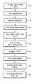
- FIG. 9is a flowchart illustrating a method of fabricating a TFT according to an embodiment of the present disclosure.
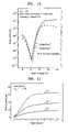
- FIG. 10is a graph illustrating electrical characteristics of a poly-Si TFT according to an embodiment of the present disclosure.
- FIG. 11is a graph illustrating a drain current with respect to a drain bias when a gate-source voltage (V GS ) of a TFT according to an embodiment of the present disclosure is 1 V, 3 V and 5V.
- V GSgate-source voltage
- ICP-CVDinductively coupled plasma chemical vapor deposition
- remote plasmawhich can reduce ion damage in a film-growth zone.
- An active layer of a poly-Si TFTis formed by the ICP-CVD.
- He/SiH 4 gas diluted with Hecan be used.
- a substrate temperature of 150° C. and a pressure of 22 mTorrare maintained.
- a ratio of He to SiH 4is 10, that is, 20:2 [sccm], and a deposition rate is 2.8 ⁇ /sec.
- FIG. 1is a graph illustrating a Raman spectrum of a deposited silicon film. Referring to FIG. 1 , it can be seen that the silicon film has a crystal structure, as indicated by a dominant peak of 520 cm ⁇ 1 . An amorphous/intermediate phase is observed in the deposited silicon film.
- the successful formation of the poly-Si filmmay be due to a reduction of ion bombardment in a film-growth zone, in which strong ions can obstruct crystal growth.
- the concentration of hydrogen in the silicon thin filmcan reach 10-12%.
- an explosive effusion phenomenon of hydrogencan occur during excimer laser annealing (ELA). Therefore, it is desirable to reduce the hydrogen concentration.
- the hydrogen concentration of the silicon film formed using the hydrogen dilutionis calculated using FT-IR. Most of the hydrogen is in the form of dihydrides, that is, Si—H 2 (2090 cm ⁇ 1 ), and some of the hydrogen is in the form of a monohydride, that is, Si—H. However, the total hydrogen concentration is merely 4%. Such a reduction of the hydrogen concentration is caused by an inert gas, He, which reduces an energy barrier of a surface reaction.
- the present embodimentinvolves the use of ELA instead of a furnace.
- excimer laser irradiationincreases stepwise from a low energy density (100 mJ/cm 2 ) to a high energy density (200 mJ/cm 2 ).
- An energy density incrementis 10 mJ/cm 2 and thus the energy density can increase 10 steps from 100 mJ/cm 2 .
- FIG. 3is a SEM photograph of an 800 ⁇ -thick poly-Si thin film with large grains produced by the above-described ELA.
- the poly-Si obtained by the ICP-CVDis recrystallized with a larger grain size by the ELA.
- FIG. 4illustrates a section of the poly-Si thin film recrystallized by the ELA. It can be observed in FIG. 4 that the poly-Si is sufficiently recrystallized and a grain boundary formed by the ELA is clear.
- Processes described beloware performed before the above two processes and are related to a method of fabricating a TFT, which is widely used as a dynamic switching device.
- an SiO 2 thin filmis formed on the poly-Si as a gate insulating layer by ICP-CVD using He gas, N 2 O gas and SiH 4 gas.
- a substrate temperatureis maintained at 150° C. and a process pressure is set to 30 mTorr.
- a contents ratio of He:N 2 O:SiH 4is 100:20:5 [sccm].
- FIG. 5is a graph illustrating a breakdown field of the gate insulating layer when RF power is 200 W, 400 W and 600 W. Referring to FIG. 5 , when the RF power is 400 W, a breakdown field is 6.2 MV/cm. Also, it can be seen that the breakdown field advantageously increases as the RF power increases.
- FIG. 6is a graph illustrating C-V characteristic of the SiO 2 thin film formed by ICP-CVD. The C-V characteristics were measured with an LCR meter at 1 MHz.
- FIG. 6illustrates the characteristics of gate insulating layers deposited with RF powers of 400 W, 450 W and 500 W under a process pressure of 25 mTorr, and with a contents ratio of He:N 2 O:SiH 4 is 100:20:5 [sccm].
- FIG. 6a flat-band voltage is below ⁇ 5 V due to charges existing in the SiO 2 thin film and its surface. As the RF power is increased, the flat-band voltage is shifted in a negative direction. The charges that exist in the interface and the SiO 2 thin film are reduced as the RF power is reduced. An effective density of an interface trap is on the order of 10 11 /cm 2 .
- FIG. 7is a graph illustrating C-V characteristic (measured with an LCR meter at 1 MHz) of two SiO 2 thin films.
- a second SiO 2 thin filmis annealed on a hot plate at a temperature of 200° C. and 400° C. Referring to FIG. 7 , as the annealing temperature is increased, the flat-band voltage and the C-V characteristic are improved. Also, an interface trap density is remarkably improved. In other words, the annealing of the SiO 2 thin film used as the gate insulating layer is required in order to obtain an excellent poly-Si TFT.
- the temperature of the annealingmust be properly adjusted in order to prevent the substrate from being deformed due to the heat generated during the annealing of the SiO 2 thin film.
- FIG. 8is a graph illustrating the C-V characteristic of the SiO 2 thin film before ELA and after ELA.
- ELA20 shots of the laser were irradiated with an energy density of 430 mJ/cm 2 .
- the flat-band voltageshifted by +1.4 V. Therefore, the charges existing in the interface or the SiO 2 thin film were reduced.
- a poly-Si film and a SiO 2 filmare fabricated at a low temperature of 150° C. Therefore, a TFT having excellent characteristics can be obtained on a heat intolerant substrate, for example, a plastic substrate.
- the plasticcan be used as the TFT substrate.
- Siis deposited on the substrate, which may be a glass substrate or plastic substrate (operation 10 ).
- ICP-CVDis performed under the conditions described above in Deposition of Silicon Thin Film, thereby forming the poly-Si silicon on the substrate.
- One technical aspect of the present disclosureis the direct attainment of the poly-Si through the deposition without any annealing.
- a source/drain impurityis implanted in the poly-Si to form an active layer (operation 11 ), and then, step-by-step ELA is performed under the conditions described above in Annealing Using ELA (operation 12 ).
- the poly-Siis patterned in the form of the active layer (operation 13 ).
- the patterningis performed by dry etching, such as a reactive ion etching (RIE).
- RIEreactive ion etching
- a SiO 2 thin film to be used as a gate insulating layeris formed under the conditions described above in Deposition of Gate Insulating Layer (operation 14 ).
- the ELAis performed on the SiO 2 thin film (operation 15 ).
- the laseris irradiated with an energy density of 120-140 mJ/cm 2 .
- a metal filmsuch as an Al film is deposited at a temperature of 120° C. (operation 16 ) and then patterned to form the gate (electrode) (operation 17 ).
- SiO 2is deposited on the resultant structure as an intermetal dielectric at a temperature of 150° C. by ICP-CVD (operation 18 ). Then, a contact hole is formed and a metallization is performed, thereby forming the poly-Si TFT (operation 19 ).
- Table 1shows sheet resistances of the doped Si thin films annealed under the different ELA conditions.
- a first rowillustrates a case when 10 shots of the excimer laser at 110 mJ/cm 2 were irradiated. In this case, the sheet resistance was 1138 ⁇ /sq.
- a second rowillustrates a case when 10 shots of the excimer laser at 120 mJ/cm 2 were irradiated. In this case, the sheet resistance was 830 ⁇ /sq.
- a third rowillustrates a case when the energy density is incrementally increased.
- the excimer laseris irradiated ten times at an energy density of 110 mJ/cm 2 , five times at 140 mJ/cm 2 , and five times at 160 mJ/cm 2 .
- the sheet resistance in this casewas 224 ⁇ /sq.
- FIGS. 10 and 11illustrate electrical characteristics of the poly-Si TFT according to an embodiment of the present disclosure and a prior art poly-Si TFT having a mobility of 100 cm 2 /Vs.
- the electrical characteristics of the TFT according to an embodiment of the present disclosureare summarized in Table 2 below.
- the maximum mobility of the TFT according to an embodiment of the present disclosureis 140 cm 2 /Vs, while the conventional mobility is 100 cm 2 /Vs. Also, the subthreshold swing is 0.52 V/dec. It is noted that an annealing or post-annealing is not performed on the TFT according to an embodiment of the present disclosure.
- an excimer laserirradiates light with an energy density of 120-140 mJ/cm 2 , preferably 130 mJ/cm 2 , the electrical characteristics of the TFT are improved, as illustrated in FIG. 10 .
- the electrical characteristicsare degraded, resulting in a large reduction in the drain current. This may result from an occurrence of a defect in the gate insulating layer resulting from the laser irradiation with the excessive energy density.
- FIG. 11is a graph illustrating a drain current with respect to a drain bias when a gate-source voltage (V GS ) of the TFT according to an embodiment of the present disclosure is 1 V, 3 V and 5V.
- V GSgate-source voltage
- three curvescorrespond to the gate-source voltages (V GS ) of 1 V, 3 V and 5 V from below, respectively.
- width and length of the gateare 20 ⁇ m and 10 ⁇ m, respectively.
- the present disclosurecan be used to produce a ploy-Si instead of a-Si by forming a Si thin film at a low temperature of 150° C. using a He/SiH 4 gas through ICP-CVD.
- a grain size of the poly-Siis large by selectively and additionally performing ELA, thereby improving electrical characteristics.
- mobility of a TFT fabricated according to an embodiment of the present disclosurecan be higher than 100 cm 2 /Vs.
- the method of fabricating a poly-Si thin film according to the present disclosurecan be applied to a flat panel display, particularly to an AMLCD (active-matrix liquid-crystal display), an AMOLED (active-matrix-organic light-emitting display), a solar cell, or a semiconductor memory, which uses a plastic substrate.
- AMLCDactive-matrix liquid-crystal display
- AMOLEDactive-matrix-organic light-emitting display
- a solar cellor a semiconductor memory
- a plastic substratewhich uses a plastic substrate.
- Such a poly-Si thin filmis adapted for use in a TFT, which requires a high mobility and fast response speed and uses a plastic substrate.
- Such a TFTcan be applied to any electronic device, including an AMLCD, an AMOLED, a switching device and an amplifying device.
Landscapes
- Engineering & Computer Science (AREA)
- Physics & Mathematics (AREA)
- Condensed Matter Physics & Semiconductors (AREA)
- General Physics & Mathematics (AREA)
- Manufacturing & Machinery (AREA)
- Computer Hardware Design (AREA)
- Microelectronics & Electronic Packaging (AREA)
- Power Engineering (AREA)
- Chemical & Material Sciences (AREA)
- Optics & Photonics (AREA)
- Crystallography & Structural Chemistry (AREA)
- Health & Medical Sciences (AREA)
- Toxicology (AREA)
- Plasma & Fusion (AREA)
- Chemical Kinetics & Catalysis (AREA)
- Materials Engineering (AREA)
- Thin Film Transistor (AREA)
- Recrystallisation Techniques (AREA)
Abstract
Description
| TABLE 1 | ||
| Laser Energy Density | Sheet Resistance | |
| (mJ/cm2) | Number of Shots | (Ω/sq) |
| 110 | 10 | 1138 |
| 120 | 10 | 830 |
| 110 + 140 + 160 | 10 + 5 + 5 | 224 |
| TABLE 2 | |||
| Typical Value | |||
| TFT Parameters | (max. or min. value) | ||
| Ion (VGS= 15 V, VDS= 5 V) [μm] | 140 (200) | ||
| Mobility [cm2/Vs] | 107 (140) | ||
| Minimum off current [nA] (VDS= 5 V) | 0.4 (0.1) | ||
| Subthreshold Swing [V/dec] | 0.76 (0.52) | ||
| On/Off | 5 × 10⁵(1 × 10⁶) | ||
Claims (5)
Priority Applications (1)
| Application Number | Priority Date | Filing Date | Title |
|---|---|---|---|
| US12/457,586US20090298268A1 (en) | 2003-12-06 | 2009-06-16 | Method of fabricating poly-crystalline silicon thin film and method of fabricating transistor using the same |
Applications Claiming Priority (2)
| Application Number | Priority Date | Filing Date | Title |
|---|---|---|---|
| KR2003-88423 | 2003-12-06 | ||
| KR1020030088423AKR20050054788A (en) | 2003-12-06 | 2003-12-06 | Fabrication method of poly-crystalline si thin film and transistor thereby |
Related Child Applications (1)
| Application Number | Title | Priority Date | Filing Date |
|---|---|---|---|
| US12/457,586DivisionUS20090298268A1 (en) | 2003-12-06 | 2009-06-16 | Method of fabricating poly-crystalline silicon thin film and method of fabricating transistor using the same |
Publications (2)
| Publication Number | Publication Date |
|---|---|
| US20060008957A1 US20060008957A1 (en) | 2006-01-12 |
| US7563659B2true US7563659B2 (en) | 2009-07-21 |
Family
ID=34737861
Family Applications (2)
| Application Number | Title | Priority Date | Filing Date |
|---|---|---|---|
| US11/003,326Expired - Fee RelatedUS7563659B2 (en) | 2003-12-06 | 2004-12-06 | Method of fabricating poly-crystalline silicon thin film and method of fabricating transistor using the same |
| US12/457,586AbandonedUS20090298268A1 (en) | 2003-12-06 | 2009-06-16 | Method of fabricating poly-crystalline silicon thin film and method of fabricating transistor using the same |
Family Applications After (1)
| Application Number | Title | Priority Date | Filing Date |
|---|---|---|---|
| US12/457,586AbandonedUS20090298268A1 (en) | 2003-12-06 | 2009-06-16 | Method of fabricating poly-crystalline silicon thin film and method of fabricating transistor using the same |
Country Status (4)
| Country | Link |
|---|---|
| US (2) | US7563659B2 (en) |
| JP (1) | JP2005175476A (en) |
| KR (1) | KR20050054788A (en) |
| CN (1) | CN100490074C (en) |
Cited By (222)
| Publication number | Priority date | Publication date | Assignee | Title |
|---|---|---|---|---|
| US20080121891A1 (en)* | 2006-09-26 | 2008-05-29 | Samsung Sdi Co., Ltd. | Method of measuring degree of crystallinity of polycrystalline silicon substrate, method of fabricating organic light emitting display using the same, and organic light emitting display fabricated using the same |
| US8163581B1 (en) | 2010-10-13 | 2012-04-24 | Monolith IC 3D | Semiconductor and optoelectronic devices |
| US8203148B2 (en) | 2010-10-11 | 2012-06-19 | Monolithic 3D Inc. | Semiconductor device and structure |
| US8237228B2 (en) | 2009-10-12 | 2012-08-07 | Monolithic 3D Inc. | System comprising a semiconductor device and structure |
| US8258810B2 (en) | 2010-09-30 | 2012-09-04 | Monolithic 3D Inc. | 3D semiconductor device |
| US8273610B2 (en) | 2010-11-18 | 2012-09-25 | Monolithic 3D Inc. | Method of constructing a semiconductor device and structure |
| US8283215B2 (en)* | 2010-10-13 | 2012-10-09 | Monolithic 3D Inc. | Semiconductor and optoelectronic devices |
| US8294159B2 (en) | 2009-10-12 | 2012-10-23 | Monolithic 3D Inc. | Method for fabrication of a semiconductor device and structure |
| US8298875B1 (en) | 2011-03-06 | 2012-10-30 | Monolithic 3D Inc. | Method for fabrication of a semiconductor device and structure |
| US8362482B2 (en) | 2009-04-14 | 2013-01-29 | Monolithic 3D Inc. | Semiconductor device and structure |
| US8362800B2 (en) | 2010-10-13 | 2013-01-29 | Monolithic 3D Inc. | 3D semiconductor device including field repairable logics |
| US8373439B2 (en) | 2009-04-14 | 2013-02-12 | Monolithic 3D Inc. | 3D semiconductor device |
| US8373230B1 (en) | 2010-10-13 | 2013-02-12 | Monolithic 3D Inc. | Method for fabrication of a semiconductor device and structure |
| US8378494B2 (en) | 2009-04-14 | 2013-02-19 | Monolithic 3D Inc. | Method for fabrication of a semiconductor device and structure |
| US8379458B1 (en) | 2010-10-13 | 2013-02-19 | Monolithic 3D Inc. | Semiconductor device and structure |
| US8378715B2 (en) | 2009-04-14 | 2013-02-19 | Monolithic 3D Inc. | Method to construct systems |
| US8384426B2 (en) | 2009-04-14 | 2013-02-26 | Monolithic 3D Inc. | Semiconductor device and structure |
| US8405420B2 (en) | 2009-04-14 | 2013-03-26 | Monolithic 3D Inc. | System comprising a semiconductor device and structure |
| US8427200B2 (en) | 2009-04-14 | 2013-04-23 | Monolithic 3D Inc. | 3D semiconductor device |
| US8440542B2 (en) | 2010-10-11 | 2013-05-14 | Monolithic 3D Inc. | Semiconductor device and structure |
| US8450804B2 (en) | 2011-03-06 | 2013-05-28 | Monolithic 3D Inc. | Semiconductor device and structure for heat removal |
| US8461035B1 (en) | 2010-09-30 | 2013-06-11 | Monolithic 3D Inc. | Method for fabrication of a semiconductor device and structure |
| US8476145B2 (en) | 2010-10-13 | 2013-07-02 | Monolithic 3D Inc. | Method of fabricating a semiconductor device and structure |
| US8492886B2 (en) | 2010-02-16 | 2013-07-23 | Monolithic 3D Inc | 3D integrated circuit with logic |
| US8536023B2 (en) | 2010-11-22 | 2013-09-17 | Monolithic 3D Inc. | Method of manufacturing a semiconductor device and structure |
| US8541819B1 (en) | 2010-12-09 | 2013-09-24 | Monolithic 3D Inc. | Semiconductor device and structure |
| US8557632B1 (en) | 2012-04-09 | 2013-10-15 | Monolithic 3D Inc. | Method for fabrication of a semiconductor device and structure |
| US8574929B1 (en) | 2012-11-16 | 2013-11-05 | Monolithic 3D Inc. | Method to form a 3D semiconductor device and structure |
| US8581349B1 (en) | 2011-05-02 | 2013-11-12 | Monolithic 3D Inc. | 3D memory semiconductor device and structure |
| US8642416B2 (en) | 2010-07-30 | 2014-02-04 | Monolithic 3D Inc. | Method of forming three dimensional integrated circuit devices using layer transfer technique |
| US8669778B1 (en) | 2009-04-14 | 2014-03-11 | Monolithic 3D Inc. | Method for design and manufacturing of a 3D semiconductor device |
| US8674470B1 (en) | 2012-12-22 | 2014-03-18 | Monolithic 3D Inc. | Semiconductor device and structure |
| US8686428B1 (en) | 2012-11-16 | 2014-04-01 | Monolithic 3D Inc. | Semiconductor device and structure |
| US8687399B2 (en) | 2011-10-02 | 2014-04-01 | Monolithic 3D Inc. | Semiconductor device and structure |
| US8709880B2 (en) | 2010-07-30 | 2014-04-29 | Monolithic 3D Inc | Method for fabrication of a semiconductor device and structure |
| US8742476B1 (en) | 2012-11-27 | 2014-06-03 | Monolithic 3D Inc. | Semiconductor device and structure |
| US8754533B2 (en) | 2009-04-14 | 2014-06-17 | Monolithic 3D Inc. | Monolithic three-dimensional semiconductor device and structure |
| US8803206B1 (en) | 2012-12-29 | 2014-08-12 | Monolithic 3D Inc. | 3D semiconductor device and structure |
| US8901613B2 (en) | 2011-03-06 | 2014-12-02 | Monolithic 3D Inc. | Semiconductor device and structure for heat removal |
| US8902663B1 (en) | 2013-03-11 | 2014-12-02 | Monolithic 3D Inc. | Method of maintaining a memory state |
| US8975670B2 (en) | 2011-03-06 | 2015-03-10 | Monolithic 3D Inc. | Semiconductor device and structure for heat removal |
| US8994404B1 (en) | 2013-03-12 | 2015-03-31 | Monolithic 3D Inc. | Semiconductor device and structure |
| US9000557B2 (en) | 2012-03-17 | 2015-04-07 | Zvi Or-Bach | Semiconductor device and structure |
| US9029173B2 (en) | 2011-10-18 | 2015-05-12 | Monolithic 3D Inc. | Method for fabrication of a semiconductor device and structure |
| US9099526B2 (en) | 2010-02-16 | 2015-08-04 | Monolithic 3D Inc. | Integrated circuit device and structure |
| US9099424B1 (en) | 2012-08-10 | 2015-08-04 | Monolithic 3D Inc. | Semiconductor system, device and structure with heat removal |
| US9117749B1 (en) | 2013-03-15 | 2015-08-25 | Monolithic 3D Inc. | Semiconductor device and structure |
| US9197804B1 (en) | 2011-10-14 | 2015-11-24 | Monolithic 3D Inc. | Semiconductor and optoelectronic devices |
| US9219005B2 (en) | 2011-06-28 | 2015-12-22 | Monolithic 3D Inc. | Semiconductor system and device |
| US9509313B2 (en) | 2009-04-14 | 2016-11-29 | Monolithic 3D Inc. | 3D semiconductor device |
| US9577642B2 (en) | 2009-04-14 | 2017-02-21 | Monolithic 3D Inc. | Method to form a 3D semiconductor device |
| US9711407B2 (en) | 2009-04-14 | 2017-07-18 | Monolithic 3D Inc. | Method of manufacturing a three dimensional integrated circuit by transfer of a mono-crystalline layer |
| US9871034B1 (en) | 2012-12-29 | 2018-01-16 | Monolithic 3D Inc. | Semiconductor device and structure |
| US9953925B2 (en) | 2011-06-28 | 2018-04-24 | Monolithic 3D Inc. | Semiconductor system and device |
| US10043781B2 (en) | 2009-10-12 | 2018-08-07 | Monolithic 3D Inc. | 3D semiconductor device and structure |
| US10115663B2 (en) | 2012-12-29 | 2018-10-30 | Monolithic 3D Inc. | 3D semiconductor device and structure |
| US10127344B2 (en) | 2013-04-15 | 2018-11-13 | Monolithic 3D Inc. | Automation for monolithic 3D devices |
| US10157909B2 (en) | 2009-10-12 | 2018-12-18 | Monolithic 3D Inc. | 3D semiconductor device and structure |
| US10217667B2 (en) | 2011-06-28 | 2019-02-26 | Monolithic 3D Inc. | 3D semiconductor device, fabrication method and system |
| US10224279B2 (en) | 2013-03-15 | 2019-03-05 | Monolithic 3D Inc. | Semiconductor device and structure |
| US10290682B2 (en) | 2010-10-11 | 2019-05-14 | Monolithic 3D Inc. | 3D IC semiconductor device and structure with stacked memory |
| US10297586B2 (en) | 2015-03-09 | 2019-05-21 | Monolithic 3D Inc. | Methods for processing a 3D semiconductor device |
| US10325651B2 (en) | 2013-03-11 | 2019-06-18 | Monolithic 3D Inc. | 3D semiconductor device with stacked memory |
| US10354995B2 (en) | 2009-10-12 | 2019-07-16 | Monolithic 3D Inc. | Semiconductor memory device and structure |
| US10366970B2 (en) | 2009-10-12 | 2019-07-30 | Monolithic 3D Inc. | 3D semiconductor device and structure |
| US10381328B2 (en) | 2015-04-19 | 2019-08-13 | Monolithic 3D Inc. | Semiconductor device and structure |
| US10388568B2 (en) | 2011-06-28 | 2019-08-20 | Monolithic 3D Inc. | 3D semiconductor device and system |
| US10388863B2 (en) | 2009-10-12 | 2019-08-20 | Monolithic 3D Inc. | 3D memory device and structure |
| US10418369B2 (en) | 2015-10-24 | 2019-09-17 | Monolithic 3D Inc. | Multi-level semiconductor memory device and structure |
| US10497713B2 (en) | 2010-11-18 | 2019-12-03 | Monolithic 3D Inc. | 3D semiconductor memory device and structure |
| US10515981B2 (en) | 2015-09-21 | 2019-12-24 | Monolithic 3D Inc. | Multilevel semiconductor device and structure with memory |
| US10522225B1 (en) | 2015-10-02 | 2019-12-31 | Monolithic 3D Inc. | Semiconductor device with non-volatile memory |
| US10600888B2 (en) | 2012-04-09 | 2020-03-24 | Monolithic 3D Inc. | 3D semiconductor device |
| US10600657B2 (en) | 2012-12-29 | 2020-03-24 | Monolithic 3D Inc | 3D semiconductor device and structure |
| US10651054B2 (en) | 2012-12-29 | 2020-05-12 | Monolithic 3D Inc. | 3D semiconductor device and structure |
| US10679977B2 (en) | 2010-10-13 | 2020-06-09 | Monolithic 3D Inc. | 3D microdisplay device and structure |
| US10825779B2 (en) | 2015-04-19 | 2020-11-03 | Monolithic 3D Inc. | 3D semiconductor device and structure |
| US10833108B2 (en) | 2010-10-13 | 2020-11-10 | Monolithic 3D Inc. | 3D microdisplay device and structure |
| US10840239B2 (en) | 2014-08-26 | 2020-11-17 | Monolithic 3D Inc. | 3D semiconductor device and structure |
| US10847540B2 (en) | 2015-10-24 | 2020-11-24 | Monolithic 3D Inc. | 3D semiconductor memory device and structure |
| US10892016B1 (en) | 2019-04-08 | 2021-01-12 | Monolithic 3D Inc. | 3D memory semiconductor devices and structures |
| US10892169B2 (en) | 2012-12-29 | 2021-01-12 | Monolithic 3D Inc. | 3D semiconductor device and structure |
| US10896931B1 (en) | 2010-10-11 | 2021-01-19 | Monolithic 3D Inc. | 3D semiconductor device and structure |
| US10903089B1 (en) | 2012-12-29 | 2021-01-26 | Monolithic 3D Inc. | 3D semiconductor device and structure |
| US10910364B2 (en) | 2009-10-12 | 2021-02-02 | Monolitaic 3D Inc. | 3D semiconductor device |
| US10943934B2 (en) | 2010-10-13 | 2021-03-09 | Monolithic 3D Inc. | Multilevel semiconductor device and structure |
| US10978501B1 (en) | 2010-10-13 | 2021-04-13 | Monolithic 3D Inc. | Multilevel semiconductor device and structure with waveguides |
| US10998374B1 (en) | 2010-10-13 | 2021-05-04 | Monolithic 3D Inc. | Multilevel semiconductor device and structure |
| US11004694B1 (en) | 2012-12-29 | 2021-05-11 | Monolithic 3D Inc. | 3D semiconductor device and structure |
| US11004719B1 (en) | 2010-11-18 | 2021-05-11 | Monolithic 3D Inc. | Methods for producing a 3D semiconductor memory device and structure |
| US11011507B1 (en) | 2015-04-19 | 2021-05-18 | Monolithic 3D Inc. | 3D semiconductor device and structure |
| US11018191B1 (en) | 2010-10-11 | 2021-05-25 | Monolithic 3D Inc. | 3D semiconductor device and structure |
| US11018133B2 (en) | 2009-10-12 | 2021-05-25 | Monolithic 3D Inc. | 3D integrated circuit |
| US11018116B2 (en) | 2012-12-22 | 2021-05-25 | Monolithic 3D Inc. | Method to form a 3D semiconductor device and structure |
| US11018042B1 (en) | 2010-11-18 | 2021-05-25 | Monolithic 3D Inc. | 3D semiconductor memory device and structure |
| US11024673B1 (en) | 2010-10-11 | 2021-06-01 | Monolithic 3D Inc. | 3D semiconductor device and structure |
| US11031394B1 (en) | 2014-01-28 | 2021-06-08 | Monolithic 3D Inc. | 3D semiconductor device and structure |
| US11030371B2 (en) | 2013-04-15 | 2021-06-08 | Monolithic 3D Inc. | Automation for monolithic 3D devices |
| US11031275B2 (en) | 2010-11-18 | 2021-06-08 | Monolithic 3D Inc. | 3D semiconductor device and structure with memory |
| US11043523B1 (en) | 2010-10-13 | 2021-06-22 | Monolithic 3D Inc. | Multilevel semiconductor device and structure with image sensors |
| US11056468B1 (en) | 2015-04-19 | 2021-07-06 | Monolithic 3D Inc. | 3D semiconductor device and structure |
| US11063024B1 (en) | 2012-12-22 | 2021-07-13 | Monlithic 3D Inc. | Method to form a 3D semiconductor device and structure |
| US11063071B1 (en) | 2010-10-13 | 2021-07-13 | Monolithic 3D Inc. | Multilevel semiconductor device and structure with waveguides |
| US11088130B2 (en) | 2014-01-28 | 2021-08-10 | Monolithic 3D Inc. | 3D semiconductor device and structure |
| US11088050B2 (en) | 2012-04-09 | 2021-08-10 | Monolithic 3D Inc. | 3D semiconductor device with isolation layers |
| US11087995B1 (en) | 2012-12-29 | 2021-08-10 | Monolithic 3D Inc. | 3D semiconductor device and structure |
| US11094576B1 (en) | 2010-11-18 | 2021-08-17 | Monolithic 3D Inc. | Methods for producing a 3D semiconductor memory device and structure |
| US11107808B1 (en) | 2014-01-28 | 2021-08-31 | Monolithic 3D Inc. | 3D semiconductor device and structure |
| US11107721B2 (en) | 2010-11-18 | 2021-08-31 | Monolithic 3D Inc. | 3D semiconductor device and structure with NAND logic |
| US11114464B2 (en) | 2015-10-24 | 2021-09-07 | Monolithic 3D Inc. | 3D semiconductor device and structure |
| US11114427B2 (en) | 2015-11-07 | 2021-09-07 | Monolithic 3D Inc. | 3D semiconductor processor and memory device and structure |
| US11121021B2 (en) | 2010-11-18 | 2021-09-14 | Monolithic 3D Inc. | 3D semiconductor device and structure |
| US11133344B2 (en) | 2010-10-13 | 2021-09-28 | Monolithic 3D Inc. | Multilevel semiconductor device and structure with image sensors |
| US11158652B1 (en) | 2019-04-08 | 2021-10-26 | Monolithic 3D Inc. | 3D memory semiconductor devices and structures |
| US11158674B2 (en) | 2010-10-11 | 2021-10-26 | Monolithic 3D Inc. | Method to produce a 3D semiconductor device and structure |
| US11164770B1 (en) | 2010-11-18 | 2021-11-02 | Monolithic 3D Inc. | Method for producing a 3D semiconductor memory device and structure |
| US11163112B2 (en) | 2010-10-13 | 2021-11-02 | Monolithic 3D Inc. | Multilevel semiconductor device and structure with electromagnetic modulators |
| US11164898B2 (en) | 2010-10-13 | 2021-11-02 | Monolithic 3D Inc. | Multilevel semiconductor device and structure |
| US11164811B2 (en) | 2012-04-09 | 2021-11-02 | Monolithic 3D Inc. | 3D semiconductor device with isolation layers and oxide-to-oxide bonding |
| US11170990B2 (en) | 2019-02-19 | 2021-11-09 | Applied Materials, Inc. | Polysilicon liners |
| US11177140B2 (en) | 2012-12-29 | 2021-11-16 | Monolithic 3D Inc. | 3D semiconductor device and structure |
| US11211279B2 (en) | 2010-11-18 | 2021-12-28 | Monolithic 3D Inc. | Method for processing a 3D integrated circuit and structure |
| US11217565B2 (en) | 2012-12-22 | 2022-01-04 | Monolithic 3D Inc. | Method to form a 3D semiconductor device and structure |
| US11227897B2 (en) | 2010-10-11 | 2022-01-18 | Monolithic 3D Inc. | Method for producing a 3D semiconductor memory device and structure |
| US11251149B2 (en) | 2016-10-10 | 2022-02-15 | Monolithic 3D Inc. | 3D memory device and structure |
| US11257867B1 (en) | 2010-10-11 | 2022-02-22 | Monolithic 3D Inc. | 3D semiconductor device and structure with oxide bonds |
| US11270055B1 (en) | 2013-04-15 | 2022-03-08 | Monolithic 3D Inc. | Automation for monolithic 3D devices |
| US11296106B2 (en) | 2019-04-08 | 2022-04-05 | Monolithic 3D Inc. | 3D memory semiconductor devices and structures |
| US11296115B1 (en) | 2015-10-24 | 2022-04-05 | Monolithic 3D Inc. | 3D semiconductor device and structure |
| US11309292B2 (en) | 2012-12-22 | 2022-04-19 | Monolithic 3D Inc. | 3D semiconductor device and structure with metal layers |
| US11315980B1 (en) | 2010-10-11 | 2022-04-26 | Monolithic 3D Inc. | 3D semiconductor device and structure with transistors |
| US11329059B1 (en) | 2016-10-10 | 2022-05-10 | Monolithic 3D Inc. | 3D memory devices and structures with thinned single crystal substrates |
| US11327227B2 (en) | 2010-10-13 | 2022-05-10 | Monolithic 3D Inc. | Multilevel semiconductor device and structure with electromagnetic modulators |
| US11341309B1 (en) | 2013-04-15 | 2022-05-24 | Monolithic 3D Inc. | Automation for monolithic 3D devices |
| US11355381B2 (en) | 2010-11-18 | 2022-06-07 | Monolithic 3D Inc. | 3D semiconductor memory device and structure |
| US11355380B2 (en) | 2010-11-18 | 2022-06-07 | Monolithic 3D Inc. | Methods for producing 3D semiconductor memory device and structure utilizing alignment marks |
| US11374118B2 (en) | 2009-10-12 | 2022-06-28 | Monolithic 3D Inc. | Method to form a 3D integrated circuit |
| US11398569B2 (en) | 2013-03-12 | 2022-07-26 | Monolithic 3D Inc. | 3D semiconductor device and structure |
| US11404466B2 (en) | 2010-10-13 | 2022-08-02 | Monolithic 3D Inc. | Multilevel semiconductor device and structure with image sensors |
| US11410912B2 (en) | 2012-04-09 | 2022-08-09 | Monolithic 3D Inc. | 3D semiconductor device with vias and isolation layers |
| US11430668B2 (en) | 2012-12-29 | 2022-08-30 | Monolithic 3D Inc. | 3D semiconductor device and structure with bonding |
| US11430667B2 (en) | 2012-12-29 | 2022-08-30 | Monolithic 3D Inc. | 3D semiconductor device and structure with bonding |
| US11437368B2 (en) | 2010-10-13 | 2022-09-06 | Monolithic 3D Inc. | Multilevel semiconductor device and structure with oxide bonding |
| US11443971B2 (en) | 2010-11-18 | 2022-09-13 | Monolithic 3D Inc. | 3D semiconductor device and structure with memory |
| US11469271B2 (en) | 2010-10-11 | 2022-10-11 | Monolithic 3D Inc. | Method to produce 3D semiconductor devices and structures with memory |
| US11476181B1 (en) | 2012-04-09 | 2022-10-18 | Monolithic 3D Inc. | 3D semiconductor device and structure with metal layers |
| US11482440B2 (en) | 2010-12-16 | 2022-10-25 | Monolithic 3D Inc. | 3D semiconductor device and structure with a built-in test circuit for repairing faulty circuits |
| US11482439B2 (en) | 2010-11-18 | 2022-10-25 | Monolithic 3D Inc. | Methods for producing a 3D semiconductor memory device comprising charge trap junction-less transistors |
| US11482438B2 (en) | 2010-11-18 | 2022-10-25 | Monolithic 3D Inc. | Methods for producing a 3D semiconductor memory device and structure |
| US11487928B2 (en) | 2013-04-15 | 2022-11-01 | Monolithic 3D Inc. | Automation for monolithic 3D devices |
| US11495484B2 (en) | 2010-11-18 | 2022-11-08 | Monolithic 3D Inc. | 3D semiconductor devices and structures with at least two single-crystal layers |
| US11508605B2 (en) | 2010-11-18 | 2022-11-22 | Monolithic 3D Inc. | 3D semiconductor memory device and structure |
| US11521888B2 (en) | 2010-11-18 | 2022-12-06 | Monolithic 3D Inc. | 3D semiconductor device and structure with high-k metal gate transistors |
| US11569117B2 (en) | 2010-11-18 | 2023-01-31 | Monolithic 3D Inc. | 3D semiconductor device and structure with single-crystal layers |
| US11574109B1 (en) | 2013-04-15 | 2023-02-07 | Monolithic 3D Inc | Automation methods for 3D integrated circuits and devices |
| US11594473B2 (en) | 2012-04-09 | 2023-02-28 | Monolithic 3D Inc. | 3D semiconductor device and structure with metal layers and a connective path |
| US11600667B1 (en) | 2010-10-11 | 2023-03-07 | Monolithic 3D Inc. | Method to produce 3D semiconductor devices and structures with memory |
| US11605663B2 (en) | 2010-10-13 | 2023-03-14 | Monolithic 3D Inc. | Multilevel semiconductor device and structure with image sensors and wafer bonding |
| US11610802B2 (en) | 2010-11-18 | 2023-03-21 | Monolithic 3D Inc. | Method for producing a 3D semiconductor device and structure with single crystal transistors and metal gate electrodes |
| US11616004B1 (en) | 2012-04-09 | 2023-03-28 | Monolithic 3D Inc. | 3D semiconductor device and structure with metal layers and a connective path |
| US11615977B2 (en) | 2010-11-18 | 2023-03-28 | Monolithic 3D Inc. | 3D semiconductor memory device and structure |
| US11694922B2 (en) | 2010-10-13 | 2023-07-04 | Monolithic 3D Inc. | Multilevel semiconductor device and structure with oxide bonding |
| US11694944B1 (en) | 2012-04-09 | 2023-07-04 | Monolithic 3D Inc. | 3D semiconductor device and structure with metal layers and a connective path |
| US11711928B2 (en) | 2016-10-10 | 2023-07-25 | Monolithic 3D Inc. | 3D memory devices and structures with control circuits |
| US11720736B2 (en) | 2013-04-15 | 2023-08-08 | Monolithic 3D Inc. | Automation methods for 3D integrated circuits and devices |
| US11735501B1 (en) | 2012-04-09 | 2023-08-22 | Monolithic 3D Inc. | 3D semiconductor device and structure with metal layers and a connective path |
| US11735462B2 (en) | 2010-11-18 | 2023-08-22 | Monolithic 3D Inc. | 3D semiconductor device and structure with single-crystal layers |
| US11763864B2 (en) | 2019-04-08 | 2023-09-19 | Monolithic 3D Inc. | 3D memory semiconductor devices and structures with bit-line pillars |
| US11784169B2 (en) | 2012-12-22 | 2023-10-10 | Monolithic 3D Inc. | 3D semiconductor device and structure with metal layers |
| US11784082B2 (en) | 2010-11-18 | 2023-10-10 | Monolithic 3D Inc. | 3D semiconductor device and structure with bonding |
| US11804396B2 (en) | 2010-11-18 | 2023-10-31 | Monolithic 3D Inc. | Methods for producing a 3D semiconductor device and structure with memory cells and multiple metal layers |
| US11812620B2 (en) | 2016-10-10 | 2023-11-07 | Monolithic 3D Inc. | 3D DRAM memory devices and structures with control circuits |
| US11855114B2 (en) | 2010-10-13 | 2023-12-26 | Monolithic 3D Inc. | Multilevel semiconductor device and structure with image sensors and wafer bonding |
| US11854857B1 (en) | 2010-11-18 | 2023-12-26 | Monolithic 3D Inc. | Methods for producing a 3D semiconductor device and structure with memory cells and multiple metal layers |
| US11855100B2 (en) | 2010-10-13 | 2023-12-26 | Monolithic 3D Inc. | Multilevel semiconductor device and structure with oxide bonding |
| US11862503B2 (en) | 2010-11-18 | 2024-01-02 | Monolithic 3D Inc. | Method for producing a 3D semiconductor device and structure with memory cells and multiple metal layers |
| US11869915B2 (en) | 2010-10-13 | 2024-01-09 | Monolithic 3D Inc. | Multilevel semiconductor device and structure with image sensors and wafer bonding |
| US11869965B2 (en) | 2013-03-11 | 2024-01-09 | Monolithic 3D Inc. | 3D semiconductor device and structure with metal layers and memory cells |
| US11869591B2 (en) | 2016-10-10 | 2024-01-09 | Monolithic 3D Inc. | 3D memory devices and structures with control circuits |
| US11881443B2 (en) | 2012-04-09 | 2024-01-23 | Monolithic 3D Inc. | 3D semiconductor device and structure with metal layers and a connective path |
| US11901210B2 (en) | 2010-11-18 | 2024-02-13 | Monolithic 3D Inc. | 3D semiconductor device and structure with memory |
| US11916045B2 (en) | 2012-12-22 | 2024-02-27 | Monolithic 3D Inc. | 3D semiconductor device and structure with metal layers |
| US11923374B2 (en) | 2013-03-12 | 2024-03-05 | Monolithic 3D Inc. | 3D semiconductor device and structure with metal layers |
| US11923230B1 (en) | 2010-11-18 | 2024-03-05 | Monolithic 3D Inc. | 3D semiconductor device and structure with bonding |
| US11929372B2 (en) | 2010-10-13 | 2024-03-12 | Monolithic 3D Inc. | Multilevel semiconductor device and structure with image sensors and wafer bonding |
| US11930648B1 (en) | 2016-10-10 | 2024-03-12 | Monolithic 3D Inc. | 3D memory devices and structures with metal layers |
| US11937422B2 (en) | 2015-11-07 | 2024-03-19 | Monolithic 3D Inc. | Semiconductor memory device and structure |
| US11935949B1 (en) | 2013-03-11 | 2024-03-19 | Monolithic 3D Inc. | 3D semiconductor device and structure with metal layers and memory cells |
| US11956952B2 (en) | 2015-08-23 | 2024-04-09 | Monolithic 3D Inc. | Semiconductor memory device and structure |
| US11961827B1 (en) | 2012-12-22 | 2024-04-16 | Monolithic 3D Inc. | 3D semiconductor device and structure with metal layers |
| US11967583B2 (en) | 2012-12-22 | 2024-04-23 | Monolithic 3D Inc. | 3D semiconductor device and structure with metal layers |
| US11978731B2 (en) | 2015-09-21 | 2024-05-07 | Monolithic 3D Inc. | Method to produce a multi-level semiconductor memory device and structure |
| US11984438B2 (en) | 2010-10-13 | 2024-05-14 | Monolithic 3D Inc. | Multilevel semiconductor device and structure with oxide bonding |
| US11984445B2 (en) | 2009-10-12 | 2024-05-14 | Monolithic 3D Inc. | 3D semiconductor devices and structures with metal layers |
| US11991884B1 (en) | 2015-10-24 | 2024-05-21 | Monolithic 3D Inc. | 3D semiconductor device and structure with logic and memory |
| US12016181B2 (en) | 2015-10-24 | 2024-06-18 | Monolithic 3D Inc. | 3D semiconductor device and structure with logic and memory |
| US12027518B1 (en) | 2009-10-12 | 2024-07-02 | Monolithic 3D Inc. | 3D semiconductor devices and structures with metal layers |
| US12035531B2 (en) | 2015-10-24 | 2024-07-09 | Monolithic 3D Inc. | 3D semiconductor device and structure with logic and memory |
| US12033884B2 (en) | 2010-11-18 | 2024-07-09 | Monolithic 3D Inc. | Methods for producing a 3D semiconductor device and structure with memory cells and multiple metal layers |
| US12051674B2 (en) | 2012-12-22 | 2024-07-30 | Monolithic 3D Inc. | 3D semiconductor device and structure with metal layers |
| US12068187B2 (en) | 2010-11-18 | 2024-08-20 | Monolithic 3D Inc. | 3D semiconductor device and structure with bonding and DRAM memory cells |
| US12080743B2 (en) | 2010-10-13 | 2024-09-03 | Monolithic 3D Inc. | Multilevel semiconductor device and structure with image sensors and wafer bonding |
| US12094829B2 (en) | 2014-01-28 | 2024-09-17 | Monolithic 3D Inc. | 3D semiconductor device and structure |
| US12094965B2 (en) | 2013-03-11 | 2024-09-17 | Monolithic 3D Inc. | 3D semiconductor device and structure with metal layers and memory cells |
| US12094892B2 (en) | 2010-10-13 | 2024-09-17 | Monolithic 3D Inc. | 3D micro display device and structure |
| US12100646B2 (en) | 2013-03-12 | 2024-09-24 | Monolithic 3D Inc. | 3D semiconductor device and structure with metal layers |
| US12100611B2 (en) | 2010-11-18 | 2024-09-24 | Monolithic 3D Inc. | Methods for producing a 3D semiconductor device and structure with memory cells and multiple metal layers |
| US12100658B2 (en) | 2015-09-21 | 2024-09-24 | Monolithic 3D Inc. | Method to produce a 3D multilayer semiconductor device and structure |
| US12120880B1 (en) | 2015-10-24 | 2024-10-15 | Monolithic 3D Inc. | 3D semiconductor device and structure with logic and memory |
| US12125737B1 (en) | 2010-11-18 | 2024-10-22 | Monolithic 3D Inc. | 3D semiconductor device and structure with metal layers and memory cells |
| US12136562B2 (en) | 2010-11-18 | 2024-11-05 | Monolithic 3D Inc. | 3D semiconductor device and structure with single-crystal layers |
| US12144190B2 (en) | 2010-11-18 | 2024-11-12 | Monolithic 3D Inc. | 3D semiconductor device and structure with bonding and memory cells preliminary class |
| US12154817B1 (en) | 2010-11-18 | 2024-11-26 | Monolithic 3D Inc. | Methods for producing a 3D semiconductor memory device and structure |
| US12178055B2 (en) | 2015-09-21 | 2024-12-24 | Monolithic 3D Inc. | 3D semiconductor memory devices and structures |
| US12219769B2 (en) | 2015-10-24 | 2025-02-04 | Monolithic 3D Inc. | 3D semiconductor device and structure with logic and memory |
| US12225704B2 (en) | 2016-10-10 | 2025-02-11 | Monolithic 3D Inc. | 3D memory devices and structures with memory arrays and metal layers |
| US12243765B2 (en) | 2010-11-18 | 2025-03-04 | Monolithic 3D Inc. | 3D semiconductor device and structure with metal layers and memory cells |
| US12249538B2 (en) | 2012-12-29 | 2025-03-11 | Monolithic 3D Inc. | 3D semiconductor device and structure including power distribution grids |
| US12250830B2 (en) | 2015-09-21 | 2025-03-11 | Monolithic 3D Inc. | 3D semiconductor memory devices and structures |
| US12272586B2 (en) | 2010-11-18 | 2025-04-08 | Monolithic 3D Inc. | 3D semiconductor memory device and structure with memory and metal layers |
| US12360310B2 (en) | 2010-10-13 | 2025-07-15 | Monolithic 3D Inc. | Multilevel semiconductor device and structure with oxide bonding |
| US12362219B2 (en) | 2010-11-18 | 2025-07-15 | Monolithic 3D Inc. | 3D semiconductor memory device and structure |
Families Citing this family (12)
| Publication number | Priority date | Publication date | Assignee | Title |
|---|---|---|---|---|
| US8178221B2 (en)* | 2000-07-10 | 2012-05-15 | Amit Goyal | {100}<100> or 45°-rotated {100}<100>, semiconductor-based, large-area, flexible, electronic devices |
| US7723242B2 (en)* | 2004-03-15 | 2010-05-25 | Sharp Laboratories Of America, Inc. | Enhanced thin-film oxidation process |
| US20060128147A1 (en)* | 2004-12-09 | 2006-06-15 | Honeywell International Inc. | Method of fabricating electrically conducting vias in a silicon wafer |
| ATE495697T1 (en)* | 2005-12-28 | 2011-02-15 | Era Endoscopy S R L | SELF-PROVING ENDOSCOPIC DEVICE |
| TWI364839B (en)* | 2006-11-17 | 2012-05-21 | Au Optronics Corp | Pixel structure of active matrix organic light emitting display and fabrication method thereof |
| CA2742128C (en)* | 2008-01-28 | 2016-11-29 | Amit Goyal | Semiconductor-based large-area flexible electronic devices |
| KR101507967B1 (en) | 2008-09-23 | 2015-04-03 | 삼성디스플레이 주식회사 | Method for forming amorphous silicon layer and method for fabricating liquid crystal display using the same |
| KR101073555B1 (en) | 2009-11-23 | 2011-10-17 | 삼성모바일디스플레이주식회사 | Laser irradiation apparatus, irradiation method thereof and crystalizing method of amorphous silicon film using the same |
| CN104538404B (en)* | 2015-01-04 | 2017-05-10 | 京东方科技集团股份有限公司 | Array substrate, manufacturing method of array substrate, display panel and display device |
| RU189283U1 (en)* | 2018-03-26 | 2019-05-17 | Частное акционерное общество "Укргидропроект" | MODULE OF GRAVITATIONAL WAVE ENERGY INSTALLATION |
| KR102548825B1 (en) | 2018-12-03 | 2023-06-29 | 삼성디스플레이 주식회사 | Laser crystalizing apparatus and method of manufacturing display apparatus |
| KR20230064677A (en) | 2021-11-03 | 2023-05-11 | 삼성디스플레이 주식회사 | Thin film transistor, method for fabricating the thin film transistor, thin film transistor array substrate, and method for fabricating the thin film transistor array substrate |
Citations (1)
| Publication number | Priority date | Publication date | Assignee | Title |
|---|---|---|---|---|
| US6312979B1 (en)* | 1998-04-28 | 2001-11-06 | Lg.Philips Lcd Co., Ltd. | Method of crystallizing an amorphous silicon layer |
Family Cites Families (12)
| Publication number | Priority date | Publication date | Assignee | Title |
|---|---|---|---|---|
| JPH07263354A (en)* | 1994-03-25 | 1995-10-13 | Kobe Steel Ltd | Formation of plasma cvd film |
| JPH0883914A (en)* | 1994-09-14 | 1996-03-26 | Toshiba Corp | Polycrystalline semiconductor device and manufacturing method thereof |
| JP3649797B2 (en)* | 1995-12-01 | 2005-05-18 | 株式会社半導体エネルギー研究所 | Semiconductor device manufacturing method |
| JPH1064816A (en)* | 1996-08-20 | 1998-03-06 | Fujitsu Ltd | Method for manufacturing semiconductor device |
| JPH10265212A (en)* | 1997-03-26 | 1998-10-06 | Nippon Telegr & Teleph Corp <Ntt> | Method for producing microcrystalline and polycrystalline silicon thin films |
| JP4174862B2 (en)* | 1998-08-04 | 2008-11-05 | ソニー株式会社 | Thin film transistor manufacturing method and semiconductor device manufacturing method |
| JP2001085701A (en)* | 1999-04-06 | 2001-03-30 | Matsushita Electric Ind Co Ltd | Device having a multilayer structure, device for manufacturing the device, and method for manufacturing the device |
| JP2001023899A (en)* | 1999-07-13 | 2001-01-26 | Hitachi Ltd | Semiconductor thin film, liquid crystal display device using the semiconductor thin film, and method of manufacturing the same |
| JP2001195011A (en)* | 2000-01-11 | 2001-07-19 | Furontekku:Kk | Thin-film transistor array substrate for display device and display device |
| US6905920B2 (en)* | 2000-09-04 | 2005-06-14 | Seiko Epson Corporation | Method for fabrication of field-effect transistor to reduce defects at MOS interfaces formed at low temperature |
| JP2002164290A (en)* | 2000-11-28 | 2002-06-07 | Tokuyama Corp | Method for manufacturing polycrystalline silicon film |
| JP2003168646A (en)* | 2001-12-04 | 2003-06-13 | Sanyo Electric Co Ltd | Method of manufacturing semiconductor device |
- 2003
- 2003-12-06KRKR1020030088423Apatent/KR20050054788A/ennot_activeCeased
- 2004
- 2004-12-06JPJP2004352198Apatent/JP2005175476A/enactivePending
- 2004-12-06USUS11/003,326patent/US7563659B2/ennot_activeExpired - Fee Related
- 2004-12-06CNCNB2004100822553Apatent/CN100490074C/ennot_activeExpired - Fee Related
- 2009
- 2009-06-16USUS12/457,586patent/US20090298268A1/ennot_activeAbandoned
Patent Citations (1)
| Publication number | Priority date | Publication date | Assignee | Title |
|---|---|---|---|---|
| US6312979B1 (en)* | 1998-04-28 | 2001-11-06 | Lg.Philips Lcd Co., Ltd. | Method of crystallizing an amorphous silicon layer |
Non-Patent Citations (3)
| Title |
|---|
| Lee et al., "Poly-Si TFT Fabricated at 150 °C Using ICP-CVD and Excimer Laser Annealing for Plastic Substrates", IEEE, pp. 8.7.1-8.7.4, Dec. 8-10, 2003. |
| S.D. Theiss, et al., "PolySilicon Thin Film Transistors Fabricated at 100°C on a Flexible Plastic Substrate", IEEE, 1998, pp. 257-260. |
| Y.J. Tung et al., "30.3: An Ultra-Low-Temperature Poly-Si TFT with Stacked Composite ECR-PECVD Gate Oxide", SID 98 Digest, 1998, pp. 887-890. |
Cited By (256)
| Publication number | Priority date | Publication date | Assignee | Title |
|---|---|---|---|---|
| US20080121891A1 (en)* | 2006-09-26 | 2008-05-29 | Samsung Sdi Co., Ltd. | Method of measuring degree of crystallinity of polycrystalline silicon substrate, method of fabricating organic light emitting display using the same, and organic light emitting display fabricated using the same |
| US7964417B2 (en) | 2006-09-26 | 2011-06-21 | Samsung Mobile Display Co., Ltd. | Method of measuring degree of crystallinity of polycrystalline silicon substrate, method of fabricating organic light emitting display using the same, and organic light emitting display fabricated using the same |
| US8427200B2 (en) | 2009-04-14 | 2013-04-23 | Monolithic 3D Inc. | 3D semiconductor device |
| US8669778B1 (en) | 2009-04-14 | 2014-03-11 | Monolithic 3D Inc. | Method for design and manufacturing of a 3D semiconductor device |
| US8754533B2 (en) | 2009-04-14 | 2014-06-17 | Monolithic 3D Inc. | Monolithic three-dimensional semiconductor device and structure |
| US8987079B2 (en) | 2009-04-14 | 2015-03-24 | Monolithic 3D Inc. | Method for developing a custom device |
| US9412645B1 (en) | 2009-04-14 | 2016-08-09 | Monolithic 3D Inc. | Semiconductor devices and structures |
| US9509313B2 (en) | 2009-04-14 | 2016-11-29 | Monolithic 3D Inc. | 3D semiconductor device |
| US8405420B2 (en) | 2009-04-14 | 2013-03-26 | Monolithic 3D Inc. | System comprising a semiconductor device and structure |
| US8384426B2 (en) | 2009-04-14 | 2013-02-26 | Monolithic 3D Inc. | Semiconductor device and structure |
| US8362482B2 (en) | 2009-04-14 | 2013-01-29 | Monolithic 3D Inc. | Semiconductor device and structure |
| US9711407B2 (en) | 2009-04-14 | 2017-07-18 | Monolithic 3D Inc. | Method of manufacturing a three dimensional integrated circuit by transfer of a mono-crystalline layer |
| US8373439B2 (en) | 2009-04-14 | 2013-02-12 | Monolithic 3D Inc. | 3D semiconductor device |
| US9577642B2 (en) | 2009-04-14 | 2017-02-21 | Monolithic 3D Inc. | Method to form a 3D semiconductor device |
| US8378494B2 (en) | 2009-04-14 | 2013-02-19 | Monolithic 3D Inc. | Method for fabrication of a semiconductor device and structure |
| US8378715B2 (en) | 2009-04-14 | 2013-02-19 | Monolithic 3D Inc. | Method to construct systems |
| US12027518B1 (en) | 2009-10-12 | 2024-07-02 | Monolithic 3D Inc. | 3D semiconductor devices and structures with metal layers |
| US10910364B2 (en) | 2009-10-12 | 2021-02-02 | Monolitaic 3D Inc. | 3D semiconductor device |
| US8395191B2 (en) | 2009-10-12 | 2013-03-12 | Monolithic 3D Inc. | Semiconductor device and structure |
| US9406670B1 (en) | 2009-10-12 | 2016-08-02 | Monolithic 3D Inc. | System comprising a semiconductor device and structure |
| US10354995B2 (en) | 2009-10-12 | 2019-07-16 | Monolithic 3D Inc. | Semiconductor memory device and structure |
| US10043781B2 (en) | 2009-10-12 | 2018-08-07 | Monolithic 3D Inc. | 3D semiconductor device and structure |
| US10388863B2 (en) | 2009-10-12 | 2019-08-20 | Monolithic 3D Inc. | 3D memory device and structure |
| US11374118B2 (en) | 2009-10-12 | 2022-06-28 | Monolithic 3D Inc. | Method to form a 3D integrated circuit |
| US10366970B2 (en) | 2009-10-12 | 2019-07-30 | Monolithic 3D Inc. | 3D semiconductor device and structure |
| US11018133B2 (en) | 2009-10-12 | 2021-05-25 | Monolithic 3D Inc. | 3D integrated circuit |
| US11984445B2 (en) | 2009-10-12 | 2024-05-14 | Monolithic 3D Inc. | 3D semiconductor devices and structures with metal layers |
| US8907442B2 (en) | 2009-10-12 | 2014-12-09 | Monolthic 3D Inc. | System comprising a semiconductor device and structure |
| US10157909B2 (en) | 2009-10-12 | 2018-12-18 | Monolithic 3D Inc. | 3D semiconductor device and structure |
| US8294159B2 (en) | 2009-10-12 | 2012-10-23 | Monolithic 3D Inc. | Method for fabrication of a semiconductor device and structure |
| US8664042B2 (en) | 2009-10-12 | 2014-03-04 | Monolithic 3D Inc. | Method for fabrication of configurable systems |
| US8237228B2 (en) | 2009-10-12 | 2012-08-07 | Monolithic 3D Inc. | System comprising a semiconductor device and structure |
| US9099526B2 (en) | 2010-02-16 | 2015-08-04 | Monolithic 3D Inc. | Integrated circuit device and structure |
| US9564432B2 (en) | 2010-02-16 | 2017-02-07 | Monolithic 3D Inc. | 3D semiconductor device and structure |
| US8492886B2 (en) | 2010-02-16 | 2013-07-23 | Monolithic 3D Inc | 3D integrated circuit with logic |
| US8846463B1 (en) | 2010-02-16 | 2014-09-30 | Monolithic 3D Inc. | Method to construct a 3D semiconductor device |
| US8709880B2 (en) | 2010-07-30 | 2014-04-29 | Monolithic 3D Inc | Method for fabrication of a semiconductor device and structure |
| US8912052B2 (en) | 2010-07-30 | 2014-12-16 | Monolithic 3D Inc. | Semiconductor device and structure |
| US8642416B2 (en) | 2010-07-30 | 2014-02-04 | Monolithic 3D Inc. | Method of forming three dimensional integrated circuit devices using layer transfer technique |
| US8703597B1 (en) | 2010-09-30 | 2014-04-22 | Monolithic 3D Inc. | Method for fabrication of a semiconductor device and structure |
| US8258810B2 (en) | 2010-09-30 | 2012-09-04 | Monolithic 3D Inc. | 3D semiconductor device |
| US8461035B1 (en) | 2010-09-30 | 2013-06-11 | Monolithic 3D Inc. | Method for fabrication of a semiconductor device and structure |
| US9419031B1 (en) | 2010-10-07 | 2016-08-16 | Monolithic 3D Inc. | Semiconductor and optoelectronic devices |
| US11600667B1 (en) | 2010-10-11 | 2023-03-07 | Monolithic 3D Inc. | Method to produce 3D semiconductor devices and structures with memory |
| US9818800B2 (en) | 2010-10-11 | 2017-11-14 | Monolithic 3D Inc. | Self aligned semiconductor device and structure |
| US10290682B2 (en) | 2010-10-11 | 2019-05-14 | Monolithic 3D Inc. | 3D IC semiconductor device and structure with stacked memory |
| US11469271B2 (en) | 2010-10-11 | 2022-10-11 | Monolithic 3D Inc. | Method to produce 3D semiconductor devices and structures with memory |
| US8203148B2 (en) | 2010-10-11 | 2012-06-19 | Monolithic 3D Inc. | Semiconductor device and structure |
| US10896931B1 (en) | 2010-10-11 | 2021-01-19 | Monolithic 3D Inc. | 3D semiconductor device and structure |
| US8440542B2 (en) | 2010-10-11 | 2013-05-14 | Monolithic 3D Inc. | Semiconductor device and structure |
| US11018191B1 (en) | 2010-10-11 | 2021-05-25 | Monolithic 3D Inc. | 3D semiconductor device and structure |
| US8956959B2 (en) | 2010-10-11 | 2015-02-17 | Monolithic 3D Inc. | Method of manufacturing a semiconductor device with two monocrystalline layers |
| US11024673B1 (en) | 2010-10-11 | 2021-06-01 | Monolithic 3D Inc. | 3D semiconductor device and structure |
| US11158674B2 (en) | 2010-10-11 | 2021-10-26 | Monolithic 3D Inc. | Method to produce a 3D semiconductor device and structure |
| US11227897B2 (en) | 2010-10-11 | 2022-01-18 | Monolithic 3D Inc. | Method for producing a 3D semiconductor memory device and structure |
| US11257867B1 (en) | 2010-10-11 | 2022-02-22 | Monolithic 3D Inc. | 3D semiconductor device and structure with oxide bonds |
| US11315980B1 (en) | 2010-10-11 | 2022-04-26 | Monolithic 3D Inc. | 3D semiconductor device and structure with transistors |
| US11694922B2 (en) | 2010-10-13 | 2023-07-04 | Monolithic 3D Inc. | Multilevel semiconductor device and structure with oxide bonding |
| US8379458B1 (en) | 2010-10-13 | 2013-02-19 | Monolithic 3D Inc. | Semiconductor device and structure |
| US11374042B1 (en) | 2010-10-13 | 2022-06-28 | Monolithic 3D Inc. | 3D micro display semiconductor device and structure |
| US11164898B2 (en) | 2010-10-13 | 2021-11-02 | Monolithic 3D Inc. | Multilevel semiconductor device and structure |
| US11163112B2 (en) | 2010-10-13 | 2021-11-02 | Monolithic 3D Inc. | Multilevel semiconductor device and structure with electromagnetic modulators |
| US11855100B2 (en) | 2010-10-13 | 2023-12-26 | Monolithic 3D Inc. | Multilevel semiconductor device and structure with oxide bonding |
| US11133344B2 (en) | 2010-10-13 | 2021-09-28 | Monolithic 3D Inc. | Multilevel semiconductor device and structure with image sensors |
| US11063071B1 (en) | 2010-10-13 | 2021-07-13 | Monolithic 3D Inc. | Multilevel semiconductor device and structure with waveguides |
| US11327227B2 (en) | 2010-10-13 | 2022-05-10 | Monolithic 3D Inc. | Multilevel semiconductor device and structure with electromagnetic modulators |
| US11855114B2 (en) | 2010-10-13 | 2023-12-26 | Monolithic 3D Inc. | Multilevel semiconductor device and structure with image sensors and wafer bonding |
| US11929372B2 (en) | 2010-10-13 | 2024-03-12 | Monolithic 3D Inc. | Multilevel semiconductor device and structure with image sensors and wafer bonding |
| US11984438B2 (en) | 2010-10-13 | 2024-05-14 | Monolithic 3D Inc. | Multilevel semiconductor device and structure with oxide bonding |
| US8476145B2 (en) | 2010-10-13 | 2013-07-02 | Monolithic 3D Inc. | Method of fabricating a semiconductor device and structure |
| US12080743B2 (en) | 2010-10-13 | 2024-09-03 | Monolithic 3D Inc. | Multilevel semiconductor device and structure with image sensors and wafer bonding |
| US11869915B2 (en) | 2010-10-13 | 2024-01-09 | Monolithic 3D Inc. | Multilevel semiconductor device and structure with image sensors and wafer bonding |
| US11404466B2 (en) | 2010-10-13 | 2022-08-02 | Monolithic 3D Inc. | Multilevel semiconductor device and structure with image sensors |
| US11043523B1 (en) | 2010-10-13 | 2021-06-22 | Monolithic 3D Inc. | Multilevel semiconductor device and structure with image sensors |
| US10998374B1 (en) | 2010-10-13 | 2021-05-04 | Monolithic 3D Inc. | Multilevel semiconductor device and structure |
| US8373230B1 (en) | 2010-10-13 | 2013-02-12 | Monolithic 3D Inc. | Method for fabrication of a semiconductor device and structure |
| US8362800B2 (en) | 2010-10-13 | 2013-01-29 | Monolithic 3D Inc. | 3D semiconductor device including field repairable logics |
| US8823122B2 (en) | 2010-10-13 | 2014-09-02 | Monolithic 3D Inc. | Semiconductor and optoelectronic devices |
| US10978501B1 (en) | 2010-10-13 | 2021-04-13 | Monolithic 3D Inc. | Multilevel semiconductor device and structure with waveguides |
| US10943934B2 (en) | 2010-10-13 | 2021-03-09 | Monolithic 3D Inc. | Multilevel semiconductor device and structure |
| US12094892B2 (en) | 2010-10-13 | 2024-09-17 | Monolithic 3D Inc. | 3D micro display device and structure |
| US8283215B2 (en)* | 2010-10-13 | 2012-10-09 | Monolithic 3D Inc. | Semiconductor and optoelectronic devices |
| US8753913B2 (en) | 2010-10-13 | 2014-06-17 | Monolithic 3D Inc. | Method for fabricating novel semiconductor and optoelectronic devices |
| US10833108B2 (en) | 2010-10-13 | 2020-11-10 | Monolithic 3D Inc. | 3D microdisplay device and structure |
| US12360310B2 (en) | 2010-10-13 | 2025-07-15 | Monolithic 3D Inc. | Multilevel semiconductor device and structure with oxide bonding |
| US10679977B2 (en) | 2010-10-13 | 2020-06-09 | Monolithic 3D Inc. | 3D microdisplay device and structure |
| US11437368B2 (en) | 2010-10-13 | 2022-09-06 | Monolithic 3D Inc. | Multilevel semiconductor device and structure with oxide bonding |
| US11605663B2 (en) | 2010-10-13 | 2023-03-14 | Monolithic 3D Inc. | Multilevel semiconductor device and structure with image sensors and wafer bonding |
| US8163581B1 (en) | 2010-10-13 | 2012-04-24 | Monolith IC 3D | Semiconductor and optoelectronic devices |
| US11615977B2 (en) | 2010-11-18 | 2023-03-28 | Monolithic 3D Inc. | 3D semiconductor memory device and structure |
| US11211279B2 (en) | 2010-11-18 | 2021-12-28 | Monolithic 3D Inc. | Method for processing a 3D integrated circuit and structure |
| US12362219B2 (en) | 2010-11-18 | 2025-07-15 | Monolithic 3D Inc. | 3D semiconductor memory device and structure |
| US8273610B2 (en) | 2010-11-18 | 2012-09-25 | Monolithic 3D Inc. | Method of constructing a semiconductor device and structure |
| US12272586B2 (en) | 2010-11-18 | 2025-04-08 | Monolithic 3D Inc. | 3D semiconductor memory device and structure with memory and metal layers |
| US11355381B2 (en) | 2010-11-18 | 2022-06-07 | Monolithic 3D Inc. | 3D semiconductor memory device and structure |
| US12243765B2 (en) | 2010-11-18 | 2025-03-04 | Monolithic 3D Inc. | 3D semiconductor device and structure with metal layers and memory cells |
| US12154817B1 (en) | 2010-11-18 | 2024-11-26 | Monolithic 3D Inc. | Methods for producing a 3D semiconductor memory device and structure |
| US10497713B2 (en) | 2010-11-18 | 2019-12-03 | Monolithic 3D Inc. | 3D semiconductor memory device and structure |
| US12144190B2 (en) | 2010-11-18 | 2024-11-12 | Monolithic 3D Inc. | 3D semiconductor device and structure with bonding and memory cells preliminary class |
| US12136562B2 (en) | 2010-11-18 | 2024-11-05 | Monolithic 3D Inc. | 3D semiconductor device and structure with single-crystal layers |
| US11355380B2 (en) | 2010-11-18 | 2022-06-07 | Monolithic 3D Inc. | Methods for producing 3D semiconductor memory device and structure utilizing alignment marks |
| US12125737B1 (en) | 2010-11-18 | 2024-10-22 | Monolithic 3D Inc. | 3D semiconductor device and structure with metal layers and memory cells |
| US12100611B2 (en) | 2010-11-18 | 2024-09-24 | Monolithic 3D Inc. | Methods for producing a 3D semiconductor device and structure with memory cells and multiple metal layers |
| US11569117B2 (en) | 2010-11-18 | 2023-01-31 | Monolithic 3D Inc. | 3D semiconductor device and structure with single-crystal layers |
| US11107721B2 (en) | 2010-11-18 | 2021-08-31 | Monolithic 3D Inc. | 3D semiconductor device and structure with NAND logic |
| US11521888B2 (en) | 2010-11-18 | 2022-12-06 | Monolithic 3D Inc. | 3D semiconductor device and structure with high-k metal gate transistors |
| US12068187B2 (en) | 2010-11-18 | 2024-08-20 | Monolithic 3D Inc. | 3D semiconductor device and structure with bonding and DRAM memory cells |
| US12033884B2 (en) | 2010-11-18 | 2024-07-09 | Monolithic 3D Inc. | Methods for producing a 3D semiconductor device and structure with memory cells and multiple metal layers |
| US11610802B2 (en) | 2010-11-18 | 2023-03-21 | Monolithic 3D Inc. | Method for producing a 3D semiconductor device and structure with single crystal transistors and metal gate electrodes |
| US11508605B2 (en) | 2010-11-18 | 2022-11-22 | Monolithic 3D Inc. | 3D semiconductor memory device and structure |
| US11443971B2 (en) | 2010-11-18 | 2022-09-13 | Monolithic 3D Inc. | 3D semiconductor device and structure with memory |
| US11495484B2 (en) | 2010-11-18 | 2022-11-08 | Monolithic 3D Inc. | 3D semiconductor devices and structures with at least two single-crystal layers |
| US11094576B1 (en) | 2010-11-18 | 2021-08-17 | Monolithic 3D Inc. | Methods for producing a 3D semiconductor memory device and structure |
| US11923230B1 (en) | 2010-11-18 | 2024-03-05 | Monolithic 3D Inc. | 3D semiconductor device and structure with bonding |
| US11901210B2 (en) | 2010-11-18 | 2024-02-13 | Monolithic 3D Inc. | 3D semiconductor device and structure with memory |
| US11121021B2 (en) | 2010-11-18 | 2021-09-14 | Monolithic 3D Inc. | 3D semiconductor device and structure |
| US11031275B2 (en) | 2010-11-18 | 2021-06-08 | Monolithic 3D Inc. | 3D semiconductor device and structure with memory |
| US11862503B2 (en) | 2010-11-18 | 2024-01-02 | Monolithic 3D Inc. | Method for producing a 3D semiconductor device and structure with memory cells and multiple metal layers |
| US11004719B1 (en) | 2010-11-18 | 2021-05-11 | Monolithic 3D Inc. | Methods for producing a 3D semiconductor memory device and structure |
| US11854857B1 (en) | 2010-11-18 | 2023-12-26 | Monolithic 3D Inc. | Methods for producing a 3D semiconductor device and structure with memory cells and multiple metal layers |
| US11482439B2 (en) | 2010-11-18 | 2022-10-25 | Monolithic 3D Inc. | Methods for producing a 3D semiconductor memory device comprising charge trap junction-less transistors |
| US11804396B2 (en) | 2010-11-18 | 2023-10-31 | Monolithic 3D Inc. | Methods for producing a 3D semiconductor device and structure with memory cells and multiple metal layers |
| US11784082B2 (en) | 2010-11-18 | 2023-10-10 | Monolithic 3D Inc. | 3D semiconductor device and structure with bonding |
| US11735462B2 (en) | 2010-11-18 | 2023-08-22 | Monolithic 3D Inc. | 3D semiconductor device and structure with single-crystal layers |
| US11018042B1 (en) | 2010-11-18 | 2021-05-25 | Monolithic 3D Inc. | 3D semiconductor memory device and structure |
| US9136153B2 (en) | 2010-11-18 | 2015-09-15 | Monolithic 3D Inc. | 3D semiconductor device and structure with back-bias |
| US11164770B1 (en) | 2010-11-18 | 2021-11-02 | Monolithic 3D Inc. | Method for producing a 3D semiconductor memory device and structure |
| US11482438B2 (en) | 2010-11-18 | 2022-10-25 | Monolithic 3D Inc. | Methods for producing a 3D semiconductor memory device and structure |
| US8536023B2 (en) | 2010-11-22 | 2013-09-17 | Monolithic 3D Inc. | Method of manufacturing a semiconductor device and structure |
| US8541819B1 (en) | 2010-12-09 | 2013-09-24 | Monolithic 3D Inc. | Semiconductor device and structure |
| US11482440B2 (en) | 2010-12-16 | 2022-10-25 | Monolithic 3D Inc. | 3D semiconductor device and structure with a built-in test circuit for repairing faulty circuits |
| US8901613B2 (en) | 2011-03-06 | 2014-12-02 | Monolithic 3D Inc. | Semiconductor device and structure for heat removal |
| US8450804B2 (en) | 2011-03-06 | 2013-05-28 | Monolithic 3D Inc. | Semiconductor device and structure for heat removal |
| US8298875B1 (en) | 2011-03-06 | 2012-10-30 | Monolithic 3D Inc. | Method for fabrication of a semiconductor device and structure |
| US8975670B2 (en) | 2011-03-06 | 2015-03-10 | Monolithic 3D Inc. | Semiconductor device and structure for heat removal |
| US8581349B1 (en) | 2011-05-02 | 2013-11-12 | Monolithic 3D Inc. | 3D memory semiconductor device and structure |
| US9219005B2 (en) | 2011-06-28 | 2015-12-22 | Monolithic 3D Inc. | Semiconductor system and device |
| US10388568B2 (en) | 2011-06-28 | 2019-08-20 | Monolithic 3D Inc. | 3D semiconductor device and system |
| US10217667B2 (en) | 2011-06-28 | 2019-02-26 | Monolithic 3D Inc. | 3D semiconductor device, fabrication method and system |
| US9953925B2 (en) | 2011-06-28 | 2018-04-24 | Monolithic 3D Inc. | Semiconductor system and device |
| US9030858B2 (en) | 2011-10-02 | 2015-05-12 | Monolithic 3D Inc. | Semiconductor device and structure |
| US8687399B2 (en) | 2011-10-02 | 2014-04-01 | Monolithic 3D Inc. | Semiconductor device and structure |
| US9197804B1 (en) | 2011-10-14 | 2015-11-24 | Monolithic 3D Inc. | Semiconductor and optoelectronic devices |
| US9029173B2 (en) | 2011-10-18 | 2015-05-12 | Monolithic 3D Inc. | Method for fabrication of a semiconductor device and structure |
| US9000557B2 (en) | 2012-03-17 | 2015-04-07 | Zvi Or-Bach | Semiconductor device and structure |
| US11164811B2 (en) | 2012-04-09 | 2021-11-02 | Monolithic 3D Inc. | 3D semiconductor device with isolation layers and oxide-to-oxide bonding |
| US11616004B1 (en) | 2012-04-09 | 2023-03-28 | Monolithic 3D Inc. | 3D semiconductor device and structure with metal layers and a connective path |
| US11735501B1 (en) | 2012-04-09 | 2023-08-22 | Monolithic 3D Inc. | 3D semiconductor device and structure with metal layers and a connective path |
| US11088050B2 (en) | 2012-04-09 | 2021-08-10 | Monolithic 3D Inc. | 3D semiconductor device with isolation layers |
| US11594473B2 (en) | 2012-04-09 | 2023-02-28 | Monolithic 3D Inc. | 3D semiconductor device and structure with metal layers and a connective path |
| US11881443B2 (en) | 2012-04-09 | 2024-01-23 | Monolithic 3D Inc. | 3D semiconductor device and structure with metal layers and a connective path |
| US11476181B1 (en) | 2012-04-09 | 2022-10-18 | Monolithic 3D Inc. | 3D semiconductor device and structure with metal layers |
| US9305867B1 (en) | 2012-04-09 | 2016-04-05 | Monolithic 3D Inc. | Semiconductor devices and structures |
| US8836073B1 (en) | 2012-04-09 | 2014-09-16 | Monolithic 3D Inc. | Semiconductor device and structure |
| US10600888B2 (en) | 2012-04-09 | 2020-03-24 | Monolithic 3D Inc. | 3D semiconductor device |
| US8557632B1 (en) | 2012-04-09 | 2013-10-15 | Monolithic 3D Inc. | Method for fabrication of a semiconductor device and structure |
| US11694944B1 (en) | 2012-04-09 | 2023-07-04 | Monolithic 3D Inc. | 3D semiconductor device and structure with metal layers and a connective path |
| US11410912B2 (en) | 2012-04-09 | 2022-08-09 | Monolithic 3D Inc. | 3D semiconductor device with vias and isolation layers |
| US9099424B1 (en) | 2012-08-10 | 2015-08-04 | Monolithic 3D Inc. | Semiconductor system, device and structure with heat removal |
| US8574929B1 (en) | 2012-11-16 | 2013-11-05 | Monolithic 3D Inc. | Method to form a 3D semiconductor device and structure |
| US8686428B1 (en) | 2012-11-16 | 2014-04-01 | Monolithic 3D Inc. | Semiconductor device and structure |
| US8742476B1 (en) | 2012-11-27 | 2014-06-03 | Monolithic 3D Inc. | Semiconductor device and structure |
| US9252134B2 (en) | 2012-12-22 | 2016-02-02 | Monolithic 3D Inc. | Semiconductor device and structure |
| US11217565B2 (en) | 2012-12-22 | 2022-01-04 | Monolithic 3D Inc. | Method to form a 3D semiconductor device and structure |
| US11916045B2 (en) | 2012-12-22 | 2024-02-27 | Monolithic 3D Inc. | 3D semiconductor device and structure with metal layers |
| US11309292B2 (en) | 2012-12-22 | 2022-04-19 | Monolithic 3D Inc. | 3D semiconductor device and structure with metal layers |
| US8674470B1 (en) | 2012-12-22 | 2014-03-18 | Monolithic 3D Inc. | Semiconductor device and structure |
| US11961827B1 (en) | 2012-12-22 | 2024-04-16 | Monolithic 3D Inc. | 3D semiconductor device and structure with metal layers |
| US12278216B2 (en) | 2012-12-22 | 2025-04-15 | Monolithic 3D Inc. | 3D semiconductor device and structure with metal layers |
| US11784169B2 (en) | 2012-12-22 | 2023-10-10 | Monolithic 3D Inc. | 3D semiconductor device and structure with metal layers |
| US8921970B1 (en) | 2012-12-22 | 2014-12-30 | Monolithic 3D Inc | Semiconductor device and structure |
| US11967583B2 (en) | 2012-12-22 | 2024-04-23 | Monolithic 3D Inc. | 3D semiconductor device and structure with metal layers |
| US11018116B2 (en) | 2012-12-22 | 2021-05-25 | Monolithic 3D Inc. | Method to form a 3D semiconductor device and structure |
| US12051674B2 (en) | 2012-12-22 | 2024-07-30 | Monolithic 3D Inc. | 3D semiconductor device and structure with metal layers |
| US11063024B1 (en) | 2012-12-22 | 2021-07-13 | Monlithic 3D Inc. | Method to form a 3D semiconductor device and structure |
| US8803206B1 (en) | 2012-12-29 | 2014-08-12 | Monolithic 3D Inc. | 3D semiconductor device and structure |
| US11430667B2 (en) | 2012-12-29 | 2022-08-30 | Monolithic 3D Inc. | 3D semiconductor device and structure with bonding |
| US11177140B2 (en) | 2012-12-29 | 2021-11-16 | Monolithic 3D Inc. | 3D semiconductor device and structure |
| US9871034B1 (en) | 2012-12-29 | 2018-01-16 | Monolithic 3D Inc. | Semiconductor device and structure |
| US10903089B1 (en) | 2012-12-29 | 2021-01-26 | Monolithic 3D Inc. | 3D semiconductor device and structure |
| US10600657B2 (en) | 2012-12-29 | 2020-03-24 | Monolithic 3D Inc | 3D semiconductor device and structure |
| US11004694B1 (en) | 2012-12-29 | 2021-05-11 | Monolithic 3D Inc. | 3D semiconductor device and structure |
| US9460991B1 (en) | 2012-12-29 | 2016-10-04 | Monolithic 3D Inc. | Semiconductor device and structure |
| US10651054B2 (en) | 2012-12-29 | 2020-05-12 | Monolithic 3D Inc. | 3D semiconductor device and structure |
| US9460978B1 (en) | 2012-12-29 | 2016-10-04 | Monolithic 3D Inc. | Semiconductor device and structure |
| US11430668B2 (en) | 2012-12-29 | 2022-08-30 | Monolithic 3D Inc. | 3D semiconductor device and structure with bonding |
| US12249538B2 (en) | 2012-12-29 | 2025-03-11 | Monolithic 3D Inc. | 3D semiconductor device and structure including power distribution grids |
| US9385058B1 (en) | 2012-12-29 | 2016-07-05 | Monolithic 3D Inc. | Semiconductor device and structure |
| US11087995B1 (en) | 2012-12-29 | 2021-08-10 | Monolithic 3D Inc. | 3D semiconductor device and structure |
| US10115663B2 (en) | 2012-12-29 | 2018-10-30 | Monolithic 3D Inc. | 3D semiconductor device and structure |
| US9911627B1 (en) | 2012-12-29 | 2018-03-06 | Monolithic 3D Inc. | Method of processing a semiconductor device |
| US10892169B2 (en) | 2012-12-29 | 2021-01-12 | Monolithic 3D Inc. | 3D semiconductor device and structure |
| US12094965B2 (en) | 2013-03-11 | 2024-09-17 | Monolithic 3D Inc. | 3D semiconductor device and structure with metal layers and memory cells |
| US11121246B2 (en) | 2013-03-11 | 2021-09-14 | Monolithic 3D Inc. | 3D semiconductor device and structure with memory |
| US11869965B2 (en) | 2013-03-11 | 2024-01-09 | Monolithic 3D Inc. | 3D semiconductor device and structure with metal layers and memory cells |
| US10355121B2 (en) | 2013-03-11 | 2019-07-16 | Monolithic 3D Inc. | 3D semiconductor device with stacked memory |
| US10964807B2 (en) | 2013-03-11 | 2021-03-30 | Monolithic 3D Inc. | 3D semiconductor device with memory |
| US10325651B2 (en) | 2013-03-11 | 2019-06-18 | Monolithic 3D Inc. | 3D semiconductor device with stacked memory |
| US8902663B1 (en) | 2013-03-11 | 2014-12-02 | Monolithic 3D Inc. | Method of maintaining a memory state |
| US11004967B1 (en) | 2013-03-11 | 2021-05-11 | Monolithic 3D Inc. | 3D semiconductor device and structure with memory |
| US11935949B1 (en) | 2013-03-11 | 2024-03-19 | Monolithic 3D Inc. | 3D semiconductor device and structure with metal layers and memory cells |
| US9496271B2 (en) | 2013-03-11 | 2016-11-15 | Monolithic 3D Inc. | 3DIC system with a two stable state memory and back-bias region |
| US11515413B2 (en) | 2013-03-11 | 2022-11-29 | Monolithic 3D Inc. | 3D semiconductor device and structure with memory |
| US11398569B2 (en) | 2013-03-12 | 2022-07-26 | Monolithic 3D Inc. | 3D semiconductor device and structure |
| US8994404B1 (en) | 2013-03-12 | 2015-03-31 | Monolithic 3D Inc. | Semiconductor device and structure |
| US12100646B2 (en) | 2013-03-12 | 2024-09-24 | Monolithic 3D Inc. | 3D semiconductor device and structure with metal layers |
| US11923374B2 (en) | 2013-03-12 | 2024-03-05 | Monolithic 3D Inc. | 3D semiconductor device and structure with metal layers |
| US9117749B1 (en) | 2013-03-15 | 2015-08-25 | Monolithic 3D Inc. | Semiconductor device and structure |
| US10224279B2 (en) | 2013-03-15 | 2019-03-05 | Monolithic 3D Inc. | Semiconductor device and structure |
| US11574109B1 (en) | 2013-04-15 | 2023-02-07 | Monolithic 3D Inc | Automation methods for 3D integrated circuits and devices |
| US11487928B2 (en) | 2013-04-15 | 2022-11-01 | Monolithic 3D Inc. | Automation for monolithic 3D devices |
| US11270055B1 (en) | 2013-04-15 | 2022-03-08 | Monolithic 3D Inc. | Automation for monolithic 3D devices |
| US11720736B2 (en) | 2013-04-15 | 2023-08-08 | Monolithic 3D Inc. | Automation methods for 3D integrated circuits and devices |
| US10127344B2 (en) | 2013-04-15 | 2018-11-13 | Monolithic 3D Inc. | Automation for monolithic 3D devices |
| US11341309B1 (en) | 2013-04-15 | 2022-05-24 | Monolithic 3D Inc. | Automation for monolithic 3D devices |
| US11030371B2 (en) | 2013-04-15 | 2021-06-08 | Monolithic 3D Inc. | Automation for monolithic 3D devices |
| US11107808B1 (en) | 2014-01-28 | 2021-08-31 | Monolithic 3D Inc. | 3D semiconductor device and structure |
| US12094829B2 (en) | 2014-01-28 | 2024-09-17 | Monolithic 3D Inc. | 3D semiconductor device and structure |
| US11088130B2 (en) | 2014-01-28 | 2021-08-10 | Monolithic 3D Inc. | 3D semiconductor device and structure |
| US11031394B1 (en) | 2014-01-28 | 2021-06-08 | Monolithic 3D Inc. | 3D semiconductor device and structure |
| US10840239B2 (en) | 2014-08-26 | 2020-11-17 | Monolithic 3D Inc. | 3D semiconductor device and structure |
| US10297586B2 (en) | 2015-03-09 | 2019-05-21 | Monolithic 3D Inc. | Methods for processing a 3D semiconductor device |
| US11011507B1 (en) | 2015-04-19 | 2021-05-18 | Monolithic 3D Inc. | 3D semiconductor device and structure |
| US10381328B2 (en) | 2015-04-19 | 2019-08-13 | Monolithic 3D Inc. | Semiconductor device and structure |
| US10825779B2 (en) | 2015-04-19 | 2020-11-03 | Monolithic 3D Inc. | 3D semiconductor device and structure |
| US11056468B1 (en) | 2015-04-19 | 2021-07-06 | Monolithic 3D Inc. | 3D semiconductor device and structure |
| US11956952B2 (en) | 2015-08-23 | 2024-04-09 | Monolithic 3D Inc. | Semiconductor memory device and structure |
| US11978731B2 (en) | 2015-09-21 | 2024-05-07 | Monolithic 3D Inc. | Method to produce a multi-level semiconductor memory device and structure |
| US12250830B2 (en) | 2015-09-21 | 2025-03-11 | Monolithic 3D Inc. | 3D semiconductor memory devices and structures |
| US12178055B2 (en) | 2015-09-21 | 2024-12-24 | Monolithic 3D Inc. | 3D semiconductor memory devices and structures |
| US10515981B2 (en) | 2015-09-21 | 2019-12-24 | Monolithic 3D Inc. | Multilevel semiconductor device and structure with memory |
| US12100658B2 (en) | 2015-09-21 | 2024-09-24 | Monolithic 3D Inc. | Method to produce a 3D multilayer semiconductor device and structure |
| US10522225B1 (en) | 2015-10-02 | 2019-12-31 | Monolithic 3D Inc. | Semiconductor device with non-volatile memory |
| US12219769B2 (en) | 2015-10-24 | 2025-02-04 | Monolithic 3D Inc. | 3D semiconductor device and structure with logic and memory |
| US12016181B2 (en) | 2015-10-24 | 2024-06-18 | Monolithic 3D Inc. | 3D semiconductor device and structure with logic and memory |
| US11296115B1 (en) | 2015-10-24 | 2022-04-05 | Monolithic 3D Inc. | 3D semiconductor device and structure |
| US11991884B1 (en) | 2015-10-24 | 2024-05-21 | Monolithic 3D Inc. | 3D semiconductor device and structure with logic and memory |
| US10847540B2 (en) | 2015-10-24 | 2020-11-24 | Monolithic 3D Inc. | 3D semiconductor memory device and structure |
| US11114464B2 (en) | 2015-10-24 | 2021-09-07 | Monolithic 3D Inc. | 3D semiconductor device and structure |
| US10418369B2 (en) | 2015-10-24 | 2019-09-17 | Monolithic 3D Inc. | Multi-level semiconductor memory device and structure |
| US12035531B2 (en) | 2015-10-24 | 2024-07-09 | Monolithic 3D Inc. | 3D semiconductor device and structure with logic and memory |
| US12120880B1 (en) | 2015-10-24 | 2024-10-15 | Monolithic 3D Inc. | 3D semiconductor device and structure with logic and memory |
| US11114427B2 (en) | 2015-11-07 | 2021-09-07 | Monolithic 3D Inc. | 3D semiconductor processor and memory device and structure |
| US11937422B2 (en) | 2015-11-07 | 2024-03-19 | Monolithic 3D Inc. | Semiconductor memory device and structure |
| US11711928B2 (en) | 2016-10-10 | 2023-07-25 | Monolithic 3D Inc. | 3D memory devices and structures with control circuits |
| US11869591B2 (en) | 2016-10-10 | 2024-01-09 | Monolithic 3D Inc. | 3D memory devices and structures with control circuits |
| US11930648B1 (en) | 2016-10-10 | 2024-03-12 | Monolithic 3D Inc. | 3D memory devices and structures with metal layers |
| US11329059B1 (en) | 2016-10-10 | 2022-05-10 | Monolithic 3D Inc. | 3D memory devices and structures with thinned single crystal substrates |
| US12225704B2 (en) | 2016-10-10 | 2025-02-11 | Monolithic 3D Inc. | 3D memory devices and structures with memory arrays and metal layers |
| US11812620B2 (en) | 2016-10-10 | 2023-11-07 | Monolithic 3D Inc. | 3D DRAM memory devices and structures with control circuits |
| US11251149B2 (en) | 2016-10-10 | 2022-02-15 | Monolithic 3D Inc. | 3D memory device and structure |
| US11170990B2 (en) | 2019-02-19 | 2021-11-09 | Applied Materials, Inc. | Polysilicon liners |
| US11763864B2 (en) | 2019-04-08 | 2023-09-19 | Monolithic 3D Inc. | 3D memory semiconductor devices and structures with bit-line pillars |
| US11296106B2 (en) | 2019-04-08 | 2022-04-05 | Monolithic 3D Inc. | 3D memory semiconductor devices and structures |
| US10892016B1 (en) | 2019-04-08 | 2021-01-12 | Monolithic 3D Inc. | 3D memory semiconductor devices and structures |
| US11158652B1 (en) | 2019-04-08 | 2021-10-26 | Monolithic 3D Inc. | 3D memory semiconductor devices and structures |
Also Published As
| Publication number | Publication date |
|---|---|
| US20060008957A1 (en) | 2006-01-12 |
| KR20050054788A (en) | 2005-06-10 |
| CN100490074C (en) | 2009-05-20 |
| US20090298268A1 (en) | 2009-12-03 |
| CN1638043A (en) | 2005-07-13 |
| JP2005175476A (en) | 2005-06-30 |
Similar Documents
| Publication | Publication Date | Title |
|---|---|---|
| US7563659B2 (en) | Method of fabricating poly-crystalline silicon thin film and method of fabricating transistor using the same | |
| US5512494A (en) | Method for manufacturing a thin film transistor having a forward staggered structure | |
| CN103026492B (en) | Thin film transistor device and method for manufacturing thin film transistor device | |
| US7871872B2 (en) | Method of manufacturing thin film transistor having lightly doped drain regions | |
| JP2004253596A (en) | Thin film transistor substrate and method of manufacturing the same | |
| US8044576B2 (en) | Organic light emitting display and method of fabricating the same | |
| US20060009014A1 (en) | Method of fabricating a poly-crystalline silicon thin film and method of fabricating a semiconductor device using the same | |
| US7982272B2 (en) | Thin-film semiconductor device and method for manufacturing the same | |
| US20050148119A1 (en) | Method of manufacturing thin film transistor, method of manufacturing flat panel display, thin film transistor, and flat panel display | |
| JP3494304B2 (en) | Method for manufacturing thin film semiconductor device | |
| US20060145158A1 (en) | Poly-crystalline silicon thin film transistor | |
| KR100695154B1 (en) | Silicon thin film transistor and method of manufacturing same | |
| JPWO2007052393A1 (en) | Semiconductor device and manufacturing method thereof | |
| JP2004288864A (en) | Thin film semiconductor, method of manufacturing thin film transistor, electro-optical device, and electronic equipment | |
| US20050263774A1 (en) | Polycrystalline Si thin film structure and fabrication method thereof and method of fabricating TFT using the same | |
| Hastas et al. | Effect of interface roughness on gate bias instability of polycrystalline silicon thin-film transistors | |
| US20060088961A1 (en) | Method of fabricating poly crystalline silicon TFT | |
| JP4222966B2 (en) | Thin film transistor and manufacturing method thereof | |
| KR100624430B1 (en) | Polycrystalline Silicon Manufacturing Method | |
| KR101100423B1 (en) | Method of forming silicon thin film transistor, gate insulating layer of silicon thin film transistor and manufacturing method of silicon thin film transistor using same | |
| JPH11284199A (en) | Semiconductor device and its manufacture | |
| CN100401484C (en) | Method for manufacturing thin film transistor | |
| US20230420254A1 (en) | Method of Fabricating Thin, Crystalline Silicon Film and Thin Film Transistors | |
| CA2638452A1 (en) | High quality ultra-thin gate dielectric | |
| JPH04186634A (en) | Manufacture of thin film semiconductor device |
Legal Events
| Date | Code | Title | Description |
|---|---|---|---|
| AS | Assignment | Owner name:SAMSUNG ELECTRONICS CO., LTD., KOREA, REPUBLIC OF Free format text:ASSIGNMENT OF ASSIGNORS INTEREST;ASSIGNORS:KWON, JANG-YEON;HAN, MIN-KOO;CHO, SE-YOUNG;AND OTHERS;REEL/FRAME:016052/0195 Effective date:20041206 | |
| FEPP | Fee payment procedure | Free format text:PAYOR NUMBER ASSIGNED (ORIGINAL EVENT CODE: ASPN); ENTITY STATUS OF PATENT OWNER: LARGE ENTITY | |
| FEPP | Fee payment procedure | Free format text:PAYER NUMBER DE-ASSIGNED (ORIGINAL EVENT CODE: RMPN); ENTITY STATUS OF PATENT OWNER: LARGE ENTITY Free format text:PAYOR NUMBER ASSIGNED (ORIGINAL EVENT CODE: ASPN); ENTITY STATUS OF PATENT OWNER: LARGE ENTITY | |
| FPAY | Fee payment | Year of fee payment:4 | |
| REMI | Maintenance fee reminder mailed | ||
| LAPS | Lapse for failure to pay maintenance fees | Free format text:PATENT EXPIRED FOR FAILURE TO PAY MAINTENANCE FEES (ORIGINAL EVENT CODE: EXP.) | |
| STCH | Information on status: patent discontinuation | Free format text:PATENT EXPIRED DUE TO NONPAYMENT OF MAINTENANCE FEES UNDER 37 CFR 1.362 | |
| FP | Lapsed due to failure to pay maintenance fee | Effective date:20170721 |