US7560318B2 - Process for forming an electronic device including semiconductor layers having different stresses - Google Patents
Process for forming an electronic device including semiconductor layers having different stressesDownload PDFInfo
- Publication number
- US7560318B2 US7560318B2US11/374,372US37437206AUS7560318B2US 7560318 B2US7560318 B2US 7560318B2US 37437206 AUS37437206 AUS 37437206AUS 7560318 B2US7560318 B2US 7560318B2
- Authority
- US
- United States
- Prior art keywords
- semiconductor layer
- workpiece
- stress
- semiconductor
- layer
- Prior art date
- Legal status (The legal status is an assumption and is not a legal conclusion. Google has not performed a legal analysis and makes no representation as to the accuracy of the status listed.)
- Expired - Fee Related, expires
Links
Images


Classifications
- H—ELECTRICITY
- H10—SEMICONDUCTOR DEVICES; ELECTRIC SOLID-STATE DEVICES NOT OTHERWISE PROVIDED FOR
- H10D—INORGANIC ELECTRIC SEMICONDUCTOR DEVICES
- H10D86/00—Integrated devices formed in or on insulating or conducting substrates, e.g. formed in silicon-on-insulator [SOI] substrates or on stainless steel or glass substrates
- H10D86/01—Manufacture or treatment
- H—ELECTRICITY
- H01—ELECTRIC ELEMENTS
- H01L—SEMICONDUCTOR DEVICES NOT COVERED BY CLASS H10
- H01L21/00—Processes or apparatus adapted for the manufacture or treatment of semiconductor or solid state devices or of parts thereof
- H01L21/02—Manufacture or treatment of semiconductor devices or of parts thereof
- H01L21/04—Manufacture or treatment of semiconductor devices or of parts thereof the devices having potential barriers, e.g. a PN junction, depletion layer or carrier concentration layer
- H01L21/18—Manufacture or treatment of semiconductor devices or of parts thereof the devices having potential barriers, e.g. a PN junction, depletion layer or carrier concentration layer the devices having semiconductor bodies comprising elements of Group IV of the Periodic Table or AIIIBV compounds with or without impurities, e.g. doping materials
- H01L21/20—Deposition of semiconductor materials on a substrate, e.g. epitaxial growth solid phase epitaxy
- H—ELECTRICITY
- H01—ELECTRIC ELEMENTS
- H01L—SEMICONDUCTOR DEVICES NOT COVERED BY CLASS H10
- H01L21/00—Processes or apparatus adapted for the manufacture or treatment of semiconductor or solid state devices or of parts thereof
- H01L21/70—Manufacture or treatment of devices consisting of a plurality of solid state components formed in or on a common substrate or of parts thereof; Manufacture of integrated circuit devices or of parts thereof
- H01L21/71—Manufacture of specific parts of devices defined in group H01L21/70
- H01L21/76—Making of isolation regions between components
- H01L21/762—Dielectric regions, e.g. EPIC dielectric isolation, LOCOS; Trench refilling techniques, SOI technology, use of channel stoppers
- H01L21/7624—Dielectric regions, e.g. EPIC dielectric isolation, LOCOS; Trench refilling techniques, SOI technology, use of channel stoppers using semiconductor on insulator [SOI] technology
- H01L21/76251—Dielectric regions, e.g. EPIC dielectric isolation, LOCOS; Trench refilling techniques, SOI technology, use of channel stoppers using semiconductor on insulator [SOI] technology using bonding techniques
- H01L21/76256—Dielectric regions, e.g. EPIC dielectric isolation, LOCOS; Trench refilling techniques, SOI technology, use of channel stoppers using semiconductor on insulator [SOI] technology using bonding techniques using silicon etch back techniques, e.g. BESOI, ELTRAN
- H—ELECTRICITY
- H10—SEMICONDUCTOR DEVICES; ELECTRIC SOLID-STATE DEVICES NOT OTHERWISE PROVIDED FOR
- H10D—INORGANIC ELECTRIC SEMICONDUCTOR DEVICES
- H10D30/00—Field-effect transistors [FET]
- H10D30/60—Insulated-gate field-effect transistors [IGFET]
- H10D30/791—Arrangements for exerting mechanical stress on the crystal lattice of the channel regions
- H—ELECTRICITY
- H10—SEMICONDUCTOR DEVICES; ELECTRIC SOLID-STATE DEVICES NOT OTHERWISE PROVIDED FOR
- H10D—INORGANIC ELECTRIC SEMICONDUCTOR DEVICES
- H10D30/00—Field-effect transistors [FET]
- H10D30/60—Insulated-gate field-effect transistors [IGFET]
- H10D30/62—Fin field-effect transistors [FinFET]
- H—ELECTRICITY
- H10—SEMICONDUCTOR DEVICES; ELECTRIC SOLID-STATE DEVICES NOT OTHERWISE PROVIDED FOR
- H10D—INORGANIC ELECTRIC SEMICONDUCTOR DEVICES
- H10D30/00—Field-effect transistors [FET]
- H10D30/60—Insulated-gate field-effect transistors [IGFET]
- H10D30/67—Thin-film transistors [TFT]
- H10D30/674—Thin-film transistors [TFT] characterised by the active materials
- H10D30/6741—Group IV materials, e.g. germanium or silicon carbide
- H10D30/6748—Group IV materials, e.g. germanium or silicon carbide having a multilayer structure or superlattice structure
- H—ELECTRICITY
- H10—SEMICONDUCTOR DEVICES; ELECTRIC SOLID-STATE DEVICES NOT OTHERWISE PROVIDED FOR
- H10D—INORGANIC ELECTRIC SEMICONDUCTOR DEVICES
- H10D86/00—Integrated devices formed in or on insulating or conducting substrates, e.g. formed in silicon-on-insulator [SOI] substrates or on stainless steel or glass substrates
- H10D86/201—Integrated devices formed in or on insulating or conducting substrates, e.g. formed in silicon-on-insulator [SOI] substrates or on stainless steel or glass substrates the substrates comprising an insulating layer on a semiconductor body, e.g. SOI
Definitions
- the present disclosurerelates to electronic devices, more particularly, to forming electronic devices with regions of different stresses and material compositions.
- Carrier mobility within an electronic component (e.g. a transistor) of an electronic devicecan be affected by the properties of the material from which the electronic component is formed. Such properties can include material composition, stress, crystal orientation, or any combination thereof. A change that improves the mobility for one carrier type can be detrimental to the mobility of a carrier of an opposing carrier type.
- CMOScomplementary metal-oxide semiconductor
- One proposed method of achieving different sets of material propertiescan include epitaxially growing a first layer of 120 nm or thicker silicon germanium (“Si (x) Ge (1 ⁇ x) ”) on a silicon wafer and annealing the silicon wafer to relax the stress in the first layer.
- a second layer of silicon formed over the relaxed Si (x) Ge (1 ⁇ x)can then have a tensile stress.
- Annealing a stressed film, such as the first layercan cause surface roughening, dislocation defects within the film, or any combination thereof.
- Such a processcould require additional processing, such as chemical mechanical polishing (“CMP”) of the surface or formation of additional Si (x) Ge (1 ⁇ x) to form a layer of sufficient quality to form a semiconductor component.
- CMPchemical mechanical polishing
- Another methodcan be to form a first graded layer of Si (x) Ge (1 ⁇ x) such that x can be close to 1 when formation of the layer begins, and gradually decrease as the layer thickens such that dislocation formation can be minimized.
- a thickness of relatively defect-free Si (x) Ge (1 ⁇ x)can be formed, and a stressed silicon layer can be formed over the first graded layer.
- Such a layercan then be transferred to another wafer by a wafer bonding and cleaving process.
- the stress in a film like the first graded layercan cause hillocks or surface roughening during the formation of the semiconductor layers or subsequent processing, possibly requiring a CMP process be performed on Si (x) Ge (1 ⁇ x) in order to facilitate the wafer bonding process.
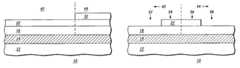
- FIG. 1includes an illustration of a cross-sectional view of a workpiece where one or more electronic components of an electronic device can be formed.
- FIG. 2includes an illustration of a cross-sectional view of the workpiece of FIG. 1 after formation of an overlying semiconductor layer.
- FIG. 3includes an illustration of a cross-sectional view of the workpiece of FIG. 2 after formation of a sacrificial layer.
- FIG. 4includes an illustration of a cross-sectional view of the workpiece of FIG. 3 after exposing a region to radiation.
- FIG. 5includes an illustration of a cross-sectional view of the workpiece of FIG. 4 after removal of a portion of a semiconductor layer.
- FIG. 6includes an illustration of a cross-sectional view of the workpiece of FIG. 5 after substantial completion of the electronic device.
- FIG. 7includes an illustration of a cross-sectional view of the workpiece of FIG. 1 after formation of a semiconductor layer according to an alternative embodiment.
- FIG. 8includes an illustration of a cross-sectional view of the workpiece of FIG. 7 after formation of a semiconductor layer.
- FIG. 9includes an illustration of a cross-section of the workpiece of FIG. 8 after removal of a portion of a semiconductor layer.
- An electronic devicecan have an insulating layer lying between a first semiconductor layer and a base layer.
- a second semiconductor layerhaving a different composition and stress as compared to the first semiconductor layer, can overlie at least a portion of the first semiconductor layer.
- a first electronic componentcan include a first active region that includes a first portion of the first and the second semiconductor layers.
- a second electronic componentcan include a second active region that can include a second portion of the first semiconductor layer.
- the stress within a channel region of the first electronic component and the stress within a channel region of the second electronic componentcan be different.
- a process of forming an electronic devicecan comprise providing a workpiece.
- the workpiececan include a first semiconductor layer, an insulating layer, and a base layer.
- the insulating layercan lie between the first semiconductor layer and the base layer.
- the first semiconductor layerhas a first stress, the first stress having a first magnitude and a first type.
- the processcan also include forming a second semiconductor layer over the first semiconductor layer, wherein the second semiconductor layer has a second stress, the second stress having a second magnitude and a second type.
- the processcan further include annealing the workpiece such that the second semiconductor layer has a third stress, the third stress having a third magnitude and a third type.
- the third magnitudecan be different than the second magnitude.
- the third magnitudecan be smaller than the second magnitude.
- the processcan also include removing at least a portion of the second semiconductor layer to expose a portion of the first semiconductor layer. After removing the at least a portion of the second semiconductor layer, the first semiconductor layer has a fourth stress, the fourth stress having a fourth magnitude and a fourth type. The fourth stress has an opposite type as compared to the second stress.
- a process of forming an electronic devicecan include providing a workpiece, wherein the workpiece can include a first semiconductor layer, an insulating layer, and a base layer.
- the insulating layercan lie between the first semiconductor layer and the base layer.
- the first semiconductor layercan have a first stress, the first stress having a first magnitude and a first type.
- the processcan also include annealing the workpiece such that the first semiconductor layer has a second stress, the second stress having a second magnitude and a second type.
- the second magnitudecan be different than the first magnitude.
- the second magnitudecan be smaller than the second magnitude.
- the processcan further include forming a second semiconductor layer overlying the first semiconductor layer, wherein the second semiconductor layer can have a third stress the third stress can have a third magnitude and a third type.
- the third stresscan have an opposite type as compared to the first stress.
- An electronic devicecan include channel regions with different stresses, and thus carrier mobility in the individual channel regions can be affected. Specific embodiments of the present disclosure will be better understood with reference to FIGS. 1 through 8 .
- active regionis intended to mean a portion of an electronic component through which charge carriers can flow during normal operation of the electronic component.
- An example of an active regioncan include source/drain and channel regions of a transistor structure or a resistive portion between terminals of a resistor.
- critical thicknessis a thickness beyond which dislocations or other defects will form to relieve stress in a layer.
- a Si (0.55) Ge (0.45) , layer formed on a monocrystaline silicon substratecan have a stress of approximately 2.5 to approximately 3.5 GPa and critical thickness between 5 and 10 nm,
- spatial orderingis intended to mean the physical arrangement of material within a solid.
- An example of spatial orderingis a lattice of a crystalline material.
- non-crystalline materialse.g. glasses, some metal alloys
- Both temperature and externally applied forcescan affect spatial ordering of a material.
- workpieceis intended to mean a substrate and, if any, one or more layers one or more structures, or any combination thereof attached to the substrate, at any particular point of a process sequence.
- the substratemay not significantly change during a process sequence, whereas the workpiece significantly changes during the process sequence.
- the substrate and workpieceare the same. After a layer is formed over the substrate, the substrate has not changed, but now the workpiece includes the combination of the substrate and the layer.
- the stress of a layeris measured at room temperature (approximately 25° C.) after formation of the layer and before a subsequent heat cycle that is greater than 100° C.
- a stresshas a magnitude (or distance from a zero value) and a type (either compressive or tensile).
- the terms “comprises,” “comprising,” “includes,” “including,” “has,” “having” or any other variation thereof,are intended to cover a non-exclusive inclusion.
- a process, method, article, or apparatus that comprises a list of elementsis not necessarily limited to only those elements but may include other elements not expressly listed or inherent to such process, method, article, or apparatus.
- “or”refers to an inclusive or and not to an exclusive or. For example, a condition A or B is satisfied by any one of the following: A is true (or present) and B is false (or not present), A is false (or not present) and B is true (or present), and both A and B are true (or present).
- FIG. 1includes an illustration of a cross-sectional view of a portion of a workpiece 10 where one or more electronic components of an electronic device can subsequently be formed.
- the workpiece 10can include a base layer 12 , an insulating layer 14 , and a semiconductor layer 16 .
- the base layer 12can be a support layer and provide mechanical support for the other layers of the workpiece.
- the base layer 12can include an insulating material typically used in manufacturing semiconductor devices such as quartz, glass, plastic, or any combination thereof.
- the base layer 12can include a semiconductor material including a semiconductor element, such as silicon, germanium, carbon, gallium, arsenic, or any combination thereof.
- the insulating layer 14can be a buried insulating layer and provide electrical insulation between the base layer 12 and the semiconductor layer 16 .
- the insulating layer 14can be grown, deposited, or otherwise formed by conventional or proprietary processing.
- the insulating layer 14can have a thickness in a range of approximately 10 to approximately 500 nm.
- the insulating layer 14can include an oxide, a nitride, an oxynitride, or any combination thereof.
- the semiconductor layer 16can be grown, deposited, otherwise formed, or bonded by a conventional or proprietary technique.
- the semiconductor layer 16can include a semiconductor element such as silicon, germanium, carbon, or any combination thereof and have a substantially uniform thickness in a range of approximately 15 to approximately 150 nm.
- the semiconductor layer 16can have a first stress.
- the semiconductor layer 16can be doped with a p-type dopant, an n-type dopant, or any combination thereof and have a dopant concentration in a range of approximately 1E14 to approximately 1E19 atoms per cubic centimeter.
- the semiconductor layer 16can include a silicon layer.
- the first stresscan have a magnitude less than approximately 10 MPa and a type that is tensile or compressive.
- field isolation regionsmay also be formed at this time.
- FIG. 2includes an illustration of a cross-sectional view of the workpiece 10 after forming a semiconductor layer 22 overlying the semiconductor layer 16 .
- the semiconductor layer 22can be grown, deposited, or otherwise formed by a conventional or proprietary process. In one embodiment, the semiconductor layer 22 can be epitaxially grown. The semiconductor layer 22 can have a thickness in a range of approximately 5 to approximately 100 nm. In one embodiment, the semiconductor layer 22 can be formed immediately adjacent to the semiconductor layer 16 . In another embodiment, the semiconductor layer 22 can include one or more semiconductor materials different from the semiconductor layer 16 . In another embodiment, the semiconductor layer 16 can include one or more semiconductor materials different from the semiconductor layer 22 .
- one of the semiconductor layers 16 or 22could be monocrystalline silicon, and the other of semiconductor layers 22 or 16 could be Si (x) Ge (1 ⁇ x) where x can be in a range of approximately 0.1 to less than 1.0.
- the semiconductor layer 22can comprise Si (x) C (1 ⁇ x) where x is in a range of approximately 0.1 to less than 1.0.
- the semiconductor layer 16can comprise a plurality of semiconductor elements, and the semiconductor layer 22 can comprise a silicon layer and be n-doped, p-doped, substantially undoped, or any combination thereof.
- a mismatch of one or more of the material properties of the semiconductor layers 16 and 22can result in a stress within the semiconductor layer 22 .
- a materialmay have a first spatial ordering at a temperature, and a second spatial ordering at a different temperature. Such a difference can be described by a thermal expansion coefficient.
- the change in spatial ordering over a temperature rangemay be different for different materials.
- a change in temperature of the workpiece 10can result in a stress within one or both of semiconductor layers 16 and 22 .
- differences in spatial orderingmay not depend on temperature changes.
- the material of the semiconductor layer 16can have a lattice constant of a different size than the material of the semiconductor layer 22 .
- epitaxially growing the semiconductor layer 22 immediately adjacent to the semiconductor layer 16can create a stress within one or both of the semiconductor layer 16 and 22 .
- the material with the smaller lattice sizecan have a tensile type of stress.
- the material with the larger lattice sizecan have a compressive type of stress.
- the semiconductor layer 22does not exceed a critical thickness with respect to the mismatch of material properties with layer 16 , such that the surface of the semiconductor layer 22 can remain substantially the same with respect to defects as before the anneal process is performed.
- the stress for the semiconductor layer 22can have a magnitude in a range of approximately 1.0 to approximately 3.5 GPa and be compressive, and have a thickness in a range of approximately 5 to approximately 50 nm.
- FIG. 3includes an illustration of a cross-sectional view of the workpiece 10 of FIG. 2 after formation of a sacrificial layer 32 .
- the sacrificial layer 32can be formed overlying the semiconductor layer 22 .
- the sacrificial layer 32can be a material selected to substantially prevent exposure of underlying layers to radiation during subsequent processing.
- the sacrificial layer 32can be an oxide, a nitride, an oxynitride, or any combination thereof.
- the sacrificial layer 32can have a thickness in a range of approximately 10 to approximately 100 nm.
- the sacrificial layer 32can be formed and patterned using a conventional or proprietary process. In one embodiment, the sacrificial layer 32 can be grown or deposited prior to patterning. The remaining portion of the sacrificial layer 32 can act as a hard mask during a subsequent anneal process.
- FIG. 4includes an illustration of a cross-sectional view of the workpiece 10 of FIG. 3 after annealing the workpiece 10 using a conventional or proprietary process to form a radiation region 42 and a radiation-protected region 44 .
- annealing the workpiece 10can utilize a directional radiation source, such as a laser source.
- annealing the workpiece 10can be performed using a rapid thermal process or anneal.
- Annealing the workpiece 10can be performed in the presence of a substantially unreactive gas such as nitrogen, helium, argon, another noble gas, or any combination thereof.
- the material composition within each of the semiconductor layer 16 and the semiconductor layer 22can remain substantially unchanged by annealing the workpiece 10 .
- the portion of the semiconductor layers 16 and 22 within the radiation region 42can have a different stress after annealing the workpiece 10 than before.
- the semiconductor layer 22can have a stress with a magnitude less than 10 MPa and be either tensile or compressive within the radiation region 42 .
- the semiconductor layer 16can have a tensile stress of greater than 10 MPa within the radiation-protected region 44 .
- sacrificial layer 32can be removed from the workpiece 10 .
- radiationcan be directed to only the radiation region 42 of the workpiece 10 .
- forming a hard mask, like sacrificial layer 32may not be required.
- sacrificial layer 32may not formed prior to annealing the workpiece 10 such that substantially all of the semiconductor layers 16 and 22 can be exposed to radiation during processing.
- FIG. 5includes an illustration of a cross-sectional view of the workpiece 10 after removal of a portion of the semiconductor layer 22 .
- the locations 52 and 54lie within the radiation region 42 and the locations 56 and 58 lie within the radiation-protected region 44 .
- the semiconductor layer 22can be patterned and etched using a conventional or proprietary process. In one embodiment, exposed material from the semiconductor layer 22 can be removed selectively to the semiconductor layer 16 .
- the exposed portions of the semiconductor layer 16 at the locations 52 and 58can have different stresses.
- the stress at location 52can be tensile and greater in magnitude than the stress at location 58 .
- the stress at location 52can be compressive and greater in magnitude than the stress at location 58 .
- the remaining portion of the semiconductor layer 22 at the locations 54 and 56can have different stresses.
- the stress at location 56can be compressive and greater in magnitude than the stress at location 54 .
- the stress at location 56can be tensile and greater in magnitude than the stress at location 54 .
- FIG. 6includes an illustration of a cross-sectional view of a substantially completed electronic device.
- An electronic componentcan be formed at each of the locations 52 , 54 , 56 , 58 , or any combination thereof.
- the electronic components at locations 52 and 58can each be formed comprising a portion of semiconductor layer 16 having a different stress.
- the semiconductor layer 16can be doped silicon and have a stress with a magnitude greater than 10 MPa with a tensile type at location 52 , and a stress with a magnitude less than 10 MPa and either a tensile or compressive type at location 58 .
- a component at location 52can have improved hole (or degraded electron) mobility over a similar device formed at location 58 .
- the electronic components at the locations 54 and 56can each be formed comprising a portion of the semiconductor layer 22 having a different stress.
- the semiconductor layer 22can be Si (x) Ge (1 ⁇ x) and have a stress with a magnitude less than 10 MPa and either a tensile or compressive type at the location 54 , and a stress with a magnitude greater than 10 MPa with a compressive type at the location 56 .
- a component at location 54can have improved hole (or degraded electron) mobility over a similar device formed at location 56 .
- fin-type structuresor a mixture of fin-type and planar structures can also be formed at the locations 52 , 54 , 56 , 58 , or any combination thereof.
- One or more gate dielectric layers, one or more gate electrodes 62 , one or more source regions, drain regions, source/drain regions 612 or any combination thereofcan be formed using a conventional or proprietary process.
- One or more insulating layers 64 , one or more conductive layers 66 , and one or more encapsulating layers 68are formed using one or more conventional or proprietary techniques. Also illustrated are previously formed field isolation regions 610 .
- the semiconductor layer 16can comprise monocrystalline silicon and the semiconductor layer 22 can comprise a Si (0.65) Ge (0.35) .
- An electronic component, such as an n-channel transistor, at location 52can have a channel region within a p-doped region with a tensile type stress with a magnitude in a range of approximately 1.0 to approximately 3.5 GPa.
- An electronic component, such as an n-channel transistor or a p-channel transistor, at location 54can have a channel region within either an n-doped or a p-doped region with either a tensile or a compressive type stress with a magnitude less than approximately 10 MPa.
- An electronic component, such as a p-channel transistor, at location 56can have a channel region within an n-doped region with a compressive type stress in a range of approximately 1.0 to approximately 3.5 GPa.
- An electronic component, such as an n-channel or p-channel transistor, at location 58can have a channel region within either an n-doped or a p-doped region with either a tensile or compressive type stress with a magnitude less than approximately 10 MPa.
- an electronic devicecan include one or more layers with a different composition, stress or any combination thereof.
- FIG. 7includes an illustration of the workpiece 20 of FIG. 1 after formation of a layer 72 .
- the layer 72can provide an element that can diffuse or otherwise migrate into the semiconductor layer 16 , and can include a material, such as silicon carbon, oxygen, germanium, or any combination thereof.
- the semiconductor layer 16can have a stress having a magnitude of less than approximately 10 MPa and a type that is either tensile or compressive.
- the layer 72can be grown, deposited or formed over the semiconductor layer 16 by a conventional or proprietary technique.
- the layer 72can include the element and have a stress having a magnitude of approximately 10 MPa or greater and, in one embodiment can have a compressive type.
- the elementcan be carbon, germanium, another semiconductor element, or any combination thereof.
- the layer 72can have a thickness in a range of approximately 5 to approximately 200 nm.
- a concentration of the element in layer 72can be higher than a concentration of the element in semiconductor layer 16 .
- the concentration of the element in the semiconductor layer 16can be substantially equal to zero.
- the workpiece 20can be heated such that a portion of the element from the layer 72 can diffuse or otherwise migrate into the semiconductor layer 16 to form the semiconductor layer 74 .
- the semiconductor layer 74can have a different concentration of the element, as compared to the semiconductor layer 16 , and the different concentration can be larger than the concentration of the element within the semiconductor layer 16 .
- the workpiece 20can be heated in a reactive environment, such an oxidizing or nitridizing environment, or the workpiece 20 can be heated in a substantially non-reacting environment, such an environment including nitrogen, helium, argon, another noble gas, or any combination thereof.
- the layer 72can then be removed from the workpiece 20 .
- the semiconductor layer 74can have a stress with a magnitude greater than approximately 10 MPa and a type that can be either compressive or tensile, depending on the element transferred between the layer 72 and the semiconductor layer 74 .
- the semiconductor layer 74can have a composition that includes the element at the different concentration.
- the semiconductor layer 74can comprise a compressively stressed silicon germanium layer with a stress in a range of approximately 1.0 to approximately 3.5 GPa and a germanium composition in a range previously discussed with respect for FIG. 2 .
- Annealing the workpiece 20can be performed on the workpiece 20 using an embodiment described with respect to the workpiece 10 in FIG. 4 such that the semiconductor layer 74 can substantially maintain the different concentration of the element and have a stress with a magnitude less than approximately 10 MPa of either a tensile or compressive type.
- FIG. 8includes an illustration of a cross-sectional view of the workpiece 20 of FIG. 7 after formation of a semiconductor layer 82 .
- the semiconductor layer 82can have a thickness in a range of approximately 5 to approximately 100 nm and include a semiconductor material.
- the semiconductor layer 82can have a different composition from the semiconductor layer 74 .
- a mismatch in material properties between the semiconductor layer 82 and the semiconductor layer 74can result in the semiconductor layer 82 having a stress.
- the stresscan be a tensile with a magnitude greater than or equal to approximately 10 MPa. In other embodiments the stress can have a compressive type.
- FIG. 9includes an illustration of a cross-sectional view of the workpiece 20 of FIG. 8 after removal of a portion of the semiconductor layer 82 .
- the locations 92 , 94 , 96 , and 98are locations where an electronic component can be formed.
- the semiconductor layer 16can comprise Si (0.65) Ge (0.35) and the stress can have a magnitude less than 10 MPa
- the semiconductor layer 82can comprise epitaxially grown silicon and the stress can be tensile and have a magnitude in a range of approximately 2.5 to approximately 3.5 GPa.
- the semiconductor layers 74 and 82can have different compositions, stresses or any combination thereof unless otherwise proscribe herein.
- processingcan continue to form a substantially complete electronic device.
- the location 52 , 54 , 56 , and 58 of the workpiece 10can correspond to locations 92 , 94 , 96 , and 98 of the workpiece 20 .
- the semiconductor layer 16 of the workpiece 10can correspond to the semiconductor layer 74 of the workpiece 20 .
- the semiconductor layer 22 of the workpiece 10can correspond to the semiconductor layer 82 of the workpiece 20 .
- An electronic component at the location 52 or the location 58can have a channel region within an n-doped region with a stress of less than approximately 10 MPa in magnitude.
- An electronic component formed at the location 54 or the location 56can have a channel region formed in a p-doped region with a stress in a range of approximately 2.5 to approximately 3.5 GPa. Formation of the remainder of the electronic device can proceed according to an embodiment previously described with respect to FIG. 6 .
- a materials mismatchcan be exploited in forming channel regions having stresses and material types tailored for a particular electronic device. Limiting the thickness of the overlying layer can introduce fewer defects and reduce the need for performing some additional processes. Channel regions closer in elevation can reduce the complexity of lithography and etch processing.
- a process of forming an electronic devicecan include providing a workpiece.
- the workpiececan include a first semiconductor layer, an insulating layer, and a base layer.
- the insulating layercan lie between the first semiconductor layer and the base layer, and the first semiconductor layer has a first stress, the first stress having a first magnitude and a first type.
- the processcan also include forming a second semiconductor layer over the first semiconductor layer, wherein the second semiconductor layer has a second stress, the second stress having a second magnitude and a second type.
- the processcan further include annealing the workpiece such that the second semiconductor layer has a third stress, the third stress having a third magnitude and a third type, wherein the third magnitude is different than the second magnitude.
- the processcan still further include removing at least a portion of the second semiconductor layer to expose a portion of the first semiconductor layer.
- the first semiconductor layerAfter removing the at least a portion of the second semiconductor layer, the first semiconductor layer has a fourth stress, the fourth stress having a fourth magnitude and a fourth type, and the fourth type is opposite the second type.
- forming the second semiconductor layerincludes forming the second semiconductor layer immediately adjacent to the first semiconductor layer. In another embodiment, forming the second semiconductor layer includes selectively forming the second semiconductor layer over only a portion of the first semiconductor layer. In a particular embodiment, annealing the workpiece includes annealing the workpiece on only a portion of the workpiece. In a more particular embodiment, annealing the workpiece on only a portion of the workpiece includes laser annealing only a portion of the workpiece.
- annealing the workpieceincludes annealing the workpiece such that the first semiconductor layer has a substantially same material composition before and after annealing the workpiece.
- Annealing the workpiecealso includes annealing the workpiece such that the second semiconductor layer has a substantially same material composition before and after annealing the workpiece.
- forming the second semiconductor layerincludes epitaxially growing a layer that includes silicon and germanium.
- the second semiconductor layerhas a thickness not greater than approximately 110 nm.
- the fourth typeis tensile. In still another embodiment, each of the first magnitude and the third magnitude is less than approximately 10 MPa.
- a process of forming an electronic devicecan include providing a workpiece, wherein the workpiece includes a first semiconductor layer, an insulating layer, and a base layer.
- the insulating layerlies between the first semiconductor layer and the base layer, and the first semiconductor layer has a first stress, the first stress having a first magnitude and a first type.
- the processcan further include annealing the workpiece such that the first semiconductor layer has a second stress, the second stress having a second magnitude and a second type, wherein the second magnitude is different than the first magnitude.
- the processcan further include forming a second semiconductor layer overlying the first semiconductor layer, wherein the second semiconductor layer has a third stress the third stress having a third magnitude and a third type, and the third type is different from the first type.
- the first typeis compressive.
- the second magnitudeis less than 10 MPa.
- forming the second semiconductor layerincludes epitaxially growing a silicon layer.
- the first semiconductor layerafter annealing the workpiece, has substantially a same composition as before annealing the workpiece.
- providing a workpiececan further include providing a workpiece, wherein the workpiece includes a third semiconductor layer.
- the insulating layercan lie between the third semiconductor layer and the base layer.
- the third semiconductorhas a fourth stress, the fourth stress having a fourth magnitude and a fourth type, and the fourth magnitude is less than approximately 10 MPa.
- the processcan further include forming a fourth semiconductor layer over the third semiconductor layer wherein the fourth semiconductor layer includes a first element.
- the processcan also include increasing the concentration of the first element within the third semiconductor layer to form the first semiconductor layer.
- the processcan further include removing the fourth semiconductor layer to expose the first semiconductor layer, wherein the first layer has the first stress.
- the first semiconductor layercan include a first semiconductor material and the first semiconductor material has a spatial ordering of a different dimension from monocrystaline silicon when the spatial ordering of each of the first semiconductor material and the monocrystalline silicon is measured at a substantially same temperature and under a substantially same combination of externally applied forces.
- an electronic devicecan include a first region that includes a first portion of a base layer.
- the electronic devicecan also include a first portion of an insulating layer overlying the first portion of the base layer.
- the electronic devicecan further include a first electronic component that includes a first active region can include a first portion of a first semiconductor layer and a first portion of a second semiconductor layer, wherein the first semiconductor layer has a different composition and a different stress compared to the second semiconductor layer.
- the electronic devicecan also include a second region that includes a second portion of the base layer.
- the electronic devicecan further include a second portion of the insulating layer overlying the second portion of the semiconductor base layer.
- the electronic devicecan still further include a second electronic component that includes a second active region can include a second portion of the first semiconductor layer but does not include any portion of the second semiconductor layer.
- the first portion of the first semiconductor layerincludes a buried channel region for an electronic component of the electronic device.
- only one of the first or the second semiconductor layerincludes tensile, monocrystaline silicon.
Landscapes
- Engineering & Computer Science (AREA)
- Physics & Mathematics (AREA)
- Condensed Matter Physics & Semiconductors (AREA)
- General Physics & Mathematics (AREA)
- Manufacturing & Machinery (AREA)
- Computer Hardware Design (AREA)
- Microelectronics & Electronic Packaging (AREA)
- Power Engineering (AREA)
- Thin Film Transistor (AREA)
- Metal-Oxide And Bipolar Metal-Oxide Semiconductor Integrated Circuits (AREA)
- Recrystallisation Techniques (AREA)
Abstract
Description
Claims (20)
Priority Applications (6)
| Application Number | Priority Date | Filing Date | Title |
|---|---|---|---|
| US11/374,372US7560318B2 (en) | 2006-03-13 | 2006-03-13 | Process for forming an electronic device including semiconductor layers having different stresses |
| EP07757297AEP1997143A4 (en) | 2006-03-13 | 2007-02-22 | ELECTRONIC DEVICE AND METHOD FOR FORMING AN ELECTRONIC DEVICE |
| KR1020087022488AKR101316556B1 (en) | 2006-03-13 | 2007-02-22 | Electronic device and a process for forming the electronic device |
| CNA2007800084096ACN101401201A (en) | 2006-03-13 | 2007-02-22 | Electronic device and a process for forming the electronic device |
| PCT/US2007/062537WO2007106646A2 (en) | 2006-03-13 | 2007-02-22 | Electronic device and a process for forming the electronic device |
| TW096107870ATWI407488B (en) | 2006-03-13 | 2007-03-07 | Electronic device and its process |
Applications Claiming Priority (1)
| Application Number | Priority Date | Filing Date | Title |
|---|---|---|---|
| US11/374,372US7560318B2 (en) | 2006-03-13 | 2006-03-13 | Process for forming an electronic device including semiconductor layers having different stresses |
Publications (2)
| Publication Number | Publication Date |
|---|---|
| US20070210381A1 US20070210381A1 (en) | 2007-09-13 |
| US7560318B2true US7560318B2 (en) | 2009-07-14 |
Family
ID=38478071
Family Applications (1)
| Application Number | Title | Priority Date | Filing Date |
|---|---|---|---|
| US11/374,372Expired - Fee RelatedUS7560318B2 (en) | 2006-03-13 | 2006-03-13 | Process for forming an electronic device including semiconductor layers having different stresses |
Country Status (6)
| Country | Link |
|---|---|
| US (1) | US7560318B2 (en) |
| EP (1) | EP1997143A4 (en) |
| KR (1) | KR101316556B1 (en) |
| CN (1) | CN101401201A (en) |
| TW (1) | TWI407488B (en) |
| WO (1) | WO2007106646A2 (en) |
Families Citing this family (2)
| Publication number | Priority date | Publication date | Assignee | Title |
|---|---|---|---|---|
| US7079712B1 (en)* | 1999-05-25 | 2006-07-18 | Silverbrook Research Pty Ltd | Method and system for providing information in a document |
| US10522418B2 (en)* | 2017-10-30 | 2019-12-31 | Taiwan Semiconductor Manufacturing Company Ltd. | Semiconductor device and method for manufacturing the same |
Citations (27)
| Publication number | Priority date | Publication date | Assignee | Title |
|---|---|---|---|---|
| US4549064A (en) | 1983-04-05 | 1985-10-22 | Fairchild Camera & Instrument Corp. | Laser treatment of silicon nitride |
| US5166084A (en) | 1991-09-03 | 1992-11-24 | Motorola, Inc. | Process for fabricating a silicon on insulator field effect transistor |
| US20040175872A1 (en) | 2003-03-07 | 2004-09-09 | Taiwan Semiconductor Manufacturing Company | Strain balanced structure with a tensile strained silicon channel and a compressive strained silicon-germanium channel for CMOS performance enhancement |
| US20040224469A1 (en) | 2003-05-08 | 2004-11-11 | The Board Of Trustees Of The University Of Illinois | Method for forming a strained semiconductor substrate |
| US20050124146A1 (en) | 2003-12-05 | 2005-06-09 | International Busiiness Machines Corporation | Method of fabricating strained Si SOI wafers |
| US20050233514A1 (en) | 2004-04-19 | 2005-10-20 | Haowen Bu | PMD liner nitride films and fabrication methods for improved NMOS performance |
| US20050255667A1 (en) | 2004-05-14 | 2005-11-17 | Applied Materials, Inc., A Delaware Corporation | Method of inducing stresses in the channel region of a transistor |
| US20050258515A1 (en) | 2004-05-21 | 2005-11-24 | International Business Machines Corporation | Embedded stressed nitride liners for CMOS performance improvement |
| US20050266639A1 (en) | 2004-05-28 | 2005-12-01 | Kai Frohberg | Techique for controlling mechanical stress in a channel region by spacer removal |
| US20060014366A1 (en) | 2002-06-07 | 2006-01-19 | Amberwave Systems Corporation | Control of strain in device layers by prevention of relaxation |
| US20060017138A1 (en) | 2004-07-13 | 2006-01-26 | Taiwan Semiconductor Manufacturing Company, Ltd. | Strain enhanced ultra shallow junction formation |
| US20060071285A1 (en) | 2004-09-29 | 2006-04-06 | Suman Datta | Inducing strain in the channels of metal gate transistors |
| US7030428B2 (en) | 2001-12-03 | 2006-04-18 | Cree, Inc. | Strain balanced nitride heterojunction transistors |
| US20060134899A1 (en) | 2004-12-21 | 2006-06-22 | Chih-Ning Wu | Method of removing spacers and fabricating mos transistor |
| US20060131268A1 (en) | 2004-12-21 | 2006-06-22 | Lam Research Corp. | Non-contact discrete removal of substrate surface contaminants/coatings, and method, apparatus, and system for implementing the same |
| US20060141687A1 (en) | 2003-02-12 | 2006-06-29 | Arup Bhattacharyya | Methods of forming semiconductor constructions |
| US20060223290A1 (en) | 2005-04-01 | 2006-10-05 | International Business Machines Corporation | Method of producing highly strained pecvd silicon nitride thin films at low temperature |
| US20060223255A1 (en) | 2004-03-10 | 2006-10-05 | Taiwan Semiconductor Manufacturing Co., Ltd. | Method for selectively stressing MOSFETs to improve charge carrier mobility |
| US20060228897A1 (en) | 2005-04-08 | 2006-10-12 | Timans Paul J | Rapid thermal processing using energy transfer layers |
| US7135392B1 (en) | 2005-07-20 | 2006-11-14 | Applied Materials, Inc. | Thermal flux laser annealing for ion implantation of semiconductor P-N junctions |
| US7145219B2 (en) | 2001-09-12 | 2006-12-05 | Reveo, Inc. | Vertical integrated circuits |
| US7161194B2 (en) | 2004-12-06 | 2007-01-09 | Cree, Inc. | High power density and/or linearity transistors |
| US7223647B2 (en) | 2004-11-05 | 2007-05-29 | Taiwan Semiconductor Manufacturing Company | Method for forming integrated advanced semiconductor device using sacrificial stress layer |
| US20070141775A1 (en) | 2005-12-15 | 2007-06-21 | Chartered Semiconductor Manufacturing, Ltd. | Modulation of stress in stress film through ion implantation and its application in stress memorization technique |
| US20070148336A1 (en) | 2005-11-07 | 2007-06-28 | Robert Bachrach | Photovoltaic contact and wiring formation |
| US20070190741A1 (en) | 2006-02-15 | 2007-08-16 | Richard Lindsay | Strained semiconductor device and method of making same |
| US20070281405A1 (en) | 2006-06-02 | 2007-12-06 | International Business Machines Corporation | Methods of stressing transistor channel with replaced gate and related structures |
Family Cites Families (4)
| Publication number | Priority date | Publication date | Assignee | Title |
|---|---|---|---|---|
| JP2005101196A (en)* | 2003-09-24 | 2005-04-14 | Hitachi Ltd | Manufacturing method of semiconductor integrated circuit device |
| US7247534B2 (en)* | 2003-11-19 | 2007-07-24 | International Business Machines Corporation | Silicon device on Si:C-OI and SGOI and method of manufacture |
| US7163903B2 (en)* | 2004-04-30 | 2007-01-16 | Freescale Semiconductor, Inc. | Method for making a semiconductor structure using silicon germanium |
| US7244958B2 (en)* | 2004-06-24 | 2007-07-17 | International Business Machines Corporation | Integration of strained Ge into advanced CMOS technology |
- 2006
- 2006-03-13USUS11/374,372patent/US7560318B2/ennot_activeExpired - Fee Related
- 2007
- 2007-02-22EPEP07757297Apatent/EP1997143A4/ennot_activeWithdrawn
- 2007-02-22WOPCT/US2007/062537patent/WO2007106646A2/enactiveApplication Filing
- 2007-02-22KRKR1020087022488Apatent/KR101316556B1/ennot_activeExpired - Fee Related
- 2007-02-22CNCNA2007800084096Apatent/CN101401201A/enactivePending
- 2007-03-07TWTW096107870Apatent/TWI407488B/ennot_activeIP Right Cessation
Patent Citations (28)
| Publication number | Priority date | Publication date | Assignee | Title |
|---|---|---|---|---|
| US4549064A (en) | 1983-04-05 | 1985-10-22 | Fairchild Camera & Instrument Corp. | Laser treatment of silicon nitride |
| US5166084A (en) | 1991-09-03 | 1992-11-24 | Motorola, Inc. | Process for fabricating a silicon on insulator field effect transistor |
| US7145219B2 (en) | 2001-09-12 | 2006-12-05 | Reveo, Inc. | Vertical integrated circuits |
| US7030428B2 (en) | 2001-12-03 | 2006-04-18 | Cree, Inc. | Strain balanced nitride heterojunction transistors |
| US20060014366A1 (en) | 2002-06-07 | 2006-01-19 | Amberwave Systems Corporation | Control of strain in device layers by prevention of relaxation |
| US20060141687A1 (en) | 2003-02-12 | 2006-06-29 | Arup Bhattacharyya | Methods of forming semiconductor constructions |
| US20040175872A1 (en) | 2003-03-07 | 2004-09-09 | Taiwan Semiconductor Manufacturing Company | Strain balanced structure with a tensile strained silicon channel and a compressive strained silicon-germanium channel for CMOS performance enhancement |
| US20040224469A1 (en) | 2003-05-08 | 2004-11-11 | The Board Of Trustees Of The University Of Illinois | Method for forming a strained semiconductor substrate |
| US20050124146A1 (en) | 2003-12-05 | 2005-06-09 | International Busiiness Machines Corporation | Method of fabricating strained Si SOI wafers |
| US20060223255A1 (en) | 2004-03-10 | 2006-10-05 | Taiwan Semiconductor Manufacturing Co., Ltd. | Method for selectively stressing MOSFETs to improve charge carrier mobility |
| US20050233514A1 (en) | 2004-04-19 | 2005-10-20 | Haowen Bu | PMD liner nitride films and fabrication methods for improved NMOS performance |
| US20050255667A1 (en) | 2004-05-14 | 2005-11-17 | Applied Materials, Inc., A Delaware Corporation | Method of inducing stresses in the channel region of a transistor |
| US20050258515A1 (en) | 2004-05-21 | 2005-11-24 | International Business Machines Corporation | Embedded stressed nitride liners for CMOS performance improvement |
| US20050266639A1 (en) | 2004-05-28 | 2005-12-01 | Kai Frohberg | Techique for controlling mechanical stress in a channel region by spacer removal |
| US20060017138A1 (en) | 2004-07-13 | 2006-01-26 | Taiwan Semiconductor Manufacturing Company, Ltd. | Strain enhanced ultra shallow junction formation |
| US7316960B2 (en) | 2004-07-13 | 2008-01-08 | Taiwan Semiconductor Manufacturing Company, Ltd. | Strain enhanced ultra shallow junction formation |
| US20060071285A1 (en) | 2004-09-29 | 2006-04-06 | Suman Datta | Inducing strain in the channels of metal gate transistors |
| US7223647B2 (en) | 2004-11-05 | 2007-05-29 | Taiwan Semiconductor Manufacturing Company | Method for forming integrated advanced semiconductor device using sacrificial stress layer |
| US7161194B2 (en) | 2004-12-06 | 2007-01-09 | Cree, Inc. | High power density and/or linearity transistors |
| US20060131268A1 (en) | 2004-12-21 | 2006-06-22 | Lam Research Corp. | Non-contact discrete removal of substrate surface contaminants/coatings, and method, apparatus, and system for implementing the same |
| US20060134899A1 (en) | 2004-12-21 | 2006-06-22 | Chih-Ning Wu | Method of removing spacers and fabricating mos transistor |
| US20060223290A1 (en) | 2005-04-01 | 2006-10-05 | International Business Machines Corporation | Method of producing highly strained pecvd silicon nitride thin films at low temperature |
| US20060228897A1 (en) | 2005-04-08 | 2006-10-12 | Timans Paul J | Rapid thermal processing using energy transfer layers |
| US7135392B1 (en) | 2005-07-20 | 2006-11-14 | Applied Materials, Inc. | Thermal flux laser annealing for ion implantation of semiconductor P-N junctions |
| US20070148336A1 (en) | 2005-11-07 | 2007-06-28 | Robert Bachrach | Photovoltaic contact and wiring formation |
| US20070141775A1 (en) | 2005-12-15 | 2007-06-21 | Chartered Semiconductor Manufacturing, Ltd. | Modulation of stress in stress film through ion implantation and its application in stress memorization technique |
| US20070190741A1 (en) | 2006-02-15 | 2007-08-16 | Richard Lindsay | Strained semiconductor device and method of making same |
| US20070281405A1 (en) | 2006-06-02 | 2007-12-06 | International Business Machines Corporation | Methods of stressing transistor channel with replaced gate and related structures |
Non-Patent Citations (3)
| Title |
|---|
| Chen et al.; "Stress memorization technique (SMT) by Selectively Strained-Nitride Capping for Sub-65nm High Performance Strained-Si Device Application" 2004 Symposium on VLSI Technology Digest of Technical Papers pp. 56-57. |
| International Search Report and Written Opinion for correlating PCT Patent Application No. PCT/US07/62537 dated Aug. 11, 2008. |
| Mishima et al.; "Ultra-thin Strained Si on Insulator Substrate Using Laser Annealing" 2005 IEEE International SOI Conference pp. 141-143. |
Also Published As
| Publication number | Publication date |
|---|---|
| WO2007106646A3 (en) | 2008-10-23 |
| US20070210381A1 (en) | 2007-09-13 |
| TWI407488B (en) | 2013-09-01 |
| KR20080111010A (en) | 2008-12-22 |
| KR101316556B1 (en) | 2013-10-15 |
| CN101401201A (en) | 2009-04-01 |
| TW200802520A (en) | 2008-01-01 |
| EP1997143A4 (en) | 2011-09-07 |
| WO2007106646A2 (en) | 2007-09-20 |
| EP1997143A2 (en) | 2008-12-03 |
Similar Documents
| Publication | Publication Date | Title |
|---|---|---|
| US7585704B2 (en) | Method of producing highly strained PECVD silicon nitride thin films at low temperature | |
| KR100818899B1 (en) | SILICON DEVICE ON SiC-OI AND SGOI AND METHOD OF MANUFACTURE | |
| US7825470B2 (en) | Transistor and in-situ fabrication process | |
| US6723541B2 (en) | Method of producing semiconductor device and semiconductor substrate | |
| US7713806B2 (en) | Structures and methods for manufacturing of dislocation free stressed channels in bulk silicon and SOI MOS devices by gate stress engineering with SiGe and/or Si:C | |
| US7566606B2 (en) | Methods of fabricating semiconductor devices having strained dual channel layers | |
| US7524740B1 (en) | Localized strain relaxation for strained Si directly on insulator | |
| US7723791B2 (en) | Strained silicon directly-on-insulator substrate with hybrid crystalline orientation and different stress levels | |
| US7615471B2 (en) | Method for producing a tensioned layer on a substrate, and a layer structure | |
| GB2469240A (en) | Fabrication of a stressed MOS device | |
| Langdo et al. | Strained Si on insulator technology: from materials to devices | |
| JPH11340337A (en) | Semiconductor device and method of manufacturing semiconductor device | |
| TW200830551A (en) | Method for providing a nanoscale, high electron mobility transistor (HEMT) on insulator | |
| US7022593B2 (en) | SiGe rectification process | |
| WO2006002410A2 (en) | Compressive sige <110> growth mosfet devices | |
| US7560318B2 (en) | Process for forming an electronic device including semiconductor layers having different stresses | |
| US20040224469A1 (en) | Method for forming a strained semiconductor substrate | |
| US9548378B2 (en) | Epitaxial channel formation methods and structures | |
| Yoshimi et al. | Strained-SOI (sSOI) technology for high-performance CMOSFETs in 45nm-or-below technology node | |
| US20110070746A1 (en) | Method of increasing operation speed and saturated current of semiconductor device and method of reducing site flatness and roughness of surface of semiconductor wafer | |
| Mooney | Improved CMOS performance via enhanced carrier mobility | |
| Mooney | Enhanced Carrier Mobility for Improved CMOS Performance |
Legal Events
| Date | Code | Title | Description |
|---|---|---|---|
| AS | Assignment | Owner name:FREESCALE SEMICONDUCTOR, INC., TEXAS Free format text:ASSIGNMENT OF ASSIGNORS INTEREST;ASSIGNORS:SADAKA, MARIAM G.;KOLAGUNTA, VENKAT R.;TAYLOR, WILLIAM J. JR.;AND OTHERS;REEL/FRAME:017653/0757;SIGNING DATES FROM 20060308 TO 20060313 | |
| AS | Assignment | Owner name:CITIBANK, N.A. AS COLLATERAL AGENT, NEW YORK Free format text:SECURITY AGREEMENT;ASSIGNORS:FREESCALE SEMICONDUCTOR, INC.;FREESCALE ACQUISITION CORPORATION;FREESCALE ACQUISITION HOLDINGS CORP.;AND OTHERS;REEL/FRAME:018855/0129 Effective date:20061201 Owner name:CITIBANK, N.A. AS COLLATERAL AGENT,NEW YORK Free format text:SECURITY AGREEMENT;ASSIGNORS:FREESCALE SEMICONDUCTOR, INC.;FREESCALE ACQUISITION CORPORATION;FREESCALE ACQUISITION HOLDINGS CORP.;AND OTHERS;REEL/FRAME:018855/0129 Effective date:20061201 | |
| FEPP | Fee payment procedure | Free format text:PAYOR NUMBER ASSIGNED (ORIGINAL EVENT CODE: ASPN); ENTITY STATUS OF PATENT OWNER: LARGE ENTITY | |
| STCF | Information on status: patent grant | Free format text:PATENTED CASE | |
| AS | Assignment | Owner name:CITIBANK, N.A.,NEW YORK Free format text:SECURITY AGREEMENT;ASSIGNOR:FREESCALE SEMICONDUCTOR, INC.;REEL/FRAME:023882/0834 Effective date:20091030 Owner name:CITIBANK, N.A., NEW YORK Free format text:SECURITY AGREEMENT;ASSIGNOR:FREESCALE SEMICONDUCTOR, INC.;REEL/FRAME:023882/0834 Effective date:20091030 | |
| AS | Assignment | Owner name:CITIBANK, N.A., AS COLLATERAL AGENT,NEW YORK Free format text:SECURITY AGREEMENT;ASSIGNOR:FREESCALE SEMICONDUCTOR, INC.;REEL/FRAME:024397/0001 Effective date:20100413 Owner name:CITIBANK, N.A., AS COLLATERAL AGENT, NEW YORK Free format text:SECURITY AGREEMENT;ASSIGNOR:FREESCALE SEMICONDUCTOR, INC.;REEL/FRAME:024397/0001 Effective date:20100413 | |
| FPAY | Fee payment | Year of fee payment:4 | |
| AS | Assignment | Owner name:CITIBANK, N.A., AS NOTES COLLATERAL AGENT, NEW YORK Free format text:SECURITY AGREEMENT;ASSIGNOR:FREESCALE SEMICONDUCTOR, INC.;REEL/FRAME:030633/0424 Effective date:20130521 Owner name:CITIBANK, N.A., AS NOTES COLLATERAL AGENT, NEW YOR Free format text:SECURITY AGREEMENT;ASSIGNOR:FREESCALE SEMICONDUCTOR, INC.;REEL/FRAME:030633/0424 Effective date:20130521 | |
| AS | Assignment | Owner name:CITIBANK, N.A., AS NOTES COLLATERAL AGENT, NEW YORK Free format text:SECURITY AGREEMENT;ASSIGNOR:FREESCALE SEMICONDUCTOR, INC.;REEL/FRAME:031591/0266 Effective date:20131101 Owner name:CITIBANK, N.A., AS NOTES COLLATERAL AGENT, NEW YOR Free format text:SECURITY AGREEMENT;ASSIGNOR:FREESCALE SEMICONDUCTOR, INC.;REEL/FRAME:031591/0266 Effective date:20131101 | |
| AS | Assignment | Owner name:FREESCALE SEMICONDUCTOR, INC., TEXAS Free format text:PATENT RELEASE;ASSIGNOR:CITIBANK, N.A., AS COLLATERAL AGENT;REEL/FRAME:037354/0854 Effective date:20151207 Owner name:FREESCALE SEMICONDUCTOR, INC., TEXAS Free format text:PATENT RELEASE;ASSIGNOR:CITIBANK, N.A., AS COLLATERAL AGENT;REEL/FRAME:037356/0143 Effective date:20151207 Owner name:FREESCALE SEMICONDUCTOR, INC., TEXAS Free format text:PATENT RELEASE;ASSIGNOR:CITIBANK, N.A., AS COLLATERAL AGENT;REEL/FRAME:037354/0225 Effective date:20151207 Owner name:FREESCALE SEMICONDUCTOR, INC., TEXAS Free format text:PATENT RELEASE;ASSIGNOR:CITIBANK, N.A., AS COLLATERAL AGENT;REEL/FRAME:037356/0553 Effective date:20151207 | |
| AS | Assignment | Owner name:MORGAN STANLEY SENIOR FUNDING, INC., MARYLAND Free format text:ASSIGNMENT AND ASSUMPTION OF SECURITY INTEREST IN PATENTS;ASSIGNOR:CITIBANK, N.A.;REEL/FRAME:037486/0517 Effective date:20151207 | |
| AS | Assignment | Owner name:MORGAN STANLEY SENIOR FUNDING, INC., MARYLAND Free format text:ASSIGNMENT AND ASSUMPTION OF SECURITY INTEREST IN PATENTS;ASSIGNOR:CITIBANK, N.A.;REEL/FRAME:037518/0292 Effective date:20151207 | |
| AS | Assignment | Owner name:MORGAN STANLEY SENIOR FUNDING, INC., MARYLAND Free format text:SECURITY AGREEMENT SUPPLEMENT;ASSIGNOR:NXP B.V.;REEL/FRAME:038017/0058 Effective date:20160218 | |
| AS | Assignment | Owner name:MORGAN STANLEY SENIOR FUNDING, INC., MARYLAND Free format text:SUPPLEMENT TO THE SECURITY AGREEMENT;ASSIGNOR:FREESCALE SEMICONDUCTOR, INC.;REEL/FRAME:039138/0001 Effective date:20160525 | |
| AS | Assignment | Owner name:MORGAN STANLEY SENIOR FUNDING, INC., MARYLAND Free format text:CORRECTIVE ASSIGNMENT TO CORRECT THE REMOVE APPLICATION 12092129 PREVIOUSLY RECORDED ON REEL 038017 FRAME 0058. ASSIGNOR(S) HEREBY CONFIRMS THE SECURITY AGREEMENT SUPPLEMENT;ASSIGNOR:NXP B.V.;REEL/FRAME:039361/0212 Effective date:20160218 | |
| AS | Assignment | Owner name:NXP, B.V., F/K/A FREESCALE SEMICONDUCTOR, INC., NETHERLANDS Free format text:RELEASE BY SECURED PARTY;ASSIGNOR:MORGAN STANLEY SENIOR FUNDING, INC.;REEL/FRAME:040925/0001 Effective date:20160912 Owner name:NXP, B.V., F/K/A FREESCALE SEMICONDUCTOR, INC., NE Free format text:RELEASE BY SECURED PARTY;ASSIGNOR:MORGAN STANLEY SENIOR FUNDING, INC.;REEL/FRAME:040925/0001 Effective date:20160912 | |
| AS | Assignment | Owner name:NXP B.V., NETHERLANDS Free format text:RELEASE BY SECURED PARTY;ASSIGNOR:MORGAN STANLEY SENIOR FUNDING, INC.;REEL/FRAME:040928/0001 Effective date:20160622 | |
| AS | Assignment | Owner name:NXP USA, INC., TEXAS Free format text:CHANGE OF NAME;ASSIGNOR:FREESCALE SEMICONDUCTOR INC.;REEL/FRAME:040652/0180 Effective date:20161107 | |
| FPAY | Fee payment | Year of fee payment:8 | |
| AS | Assignment | Owner name:NXP USA, INC., TEXAS Free format text:CORRECTIVE ASSIGNMENT TO CORRECT THE NATURE OF CONVEYANCE LISTED CHANGE OF NAME SHOULD BE MERGER AND CHANGE PREVIOUSLY RECORDED AT REEL: 040652 FRAME: 0180. ASSIGNOR(S) HEREBY CONFIRMS THE MERGER AND CHANGE OF NAME;ASSIGNOR:FREESCALE SEMICONDUCTOR INC.;REEL/FRAME:041354/0148 Effective date:20161107 | |
| AS | Assignment | Owner name:MORGAN STANLEY SENIOR FUNDING, INC., MARYLAND Free format text:CORRECTIVE ASSIGNMENT TO CORRECT THE REMOVE PATENTS 8108266 AND 8062324 AND REPLACE THEM WITH 6108266 AND 8060324 PREVIOUSLY RECORDED ON REEL 037518 FRAME 0292. ASSIGNOR(S) HEREBY CONFIRMS THE ASSIGNMENT AND ASSUMPTION OF SECURITY INTEREST IN PATENTS;ASSIGNOR:CITIBANK, N.A.;REEL/FRAME:041703/0536 Effective date:20151207 | |
| AS | Assignment | Owner name:MORGAN STANLEY SENIOR FUNDING, INC., MARYLAND Free format text:CORRECTIVE ASSIGNMENT TO CORRECT THE REMOVE APPLICATION 12681366 PREVIOUSLY RECORDED ON REEL 039361 FRAME 0212. ASSIGNOR(S) HEREBY CONFIRMS THE SECURITY AGREEMENT SUPPLEMENT;ASSIGNOR:NXP B.V.;REEL/FRAME:042762/0145 Effective date:20160218 Owner name:MORGAN STANLEY SENIOR FUNDING, INC., MARYLAND Free format text:CORRECTIVE ASSIGNMENT TO CORRECT THE REMOVE APPLICATION 12681366 PREVIOUSLY RECORDED ON REEL 038017 FRAME 0058. ASSIGNOR(S) HEREBY CONFIRMS THE SECURITY AGREEMENT SUPPLEMENT;ASSIGNOR:NXP B.V.;REEL/FRAME:042985/0001 Effective date:20160218 | |
| AS | Assignment | Owner name:SHENZHEN XINGUODU TECHNOLOGY CO., LTD., CHINA Free format text:CORRECTIVE ASSIGNMENT TO CORRECT THE TO CORRECT THE APPLICATION NO. FROM 13,883,290 TO 13,833,290 PREVIOUSLY RECORDED ON REEL 041703 FRAME 0536. ASSIGNOR(S) HEREBY CONFIRMS THE THE ASSIGNMENT AND ASSUMPTION OF SECURITYINTEREST IN PATENTS.;ASSIGNOR:MORGAN STANLEY SENIOR FUNDING, INC.;REEL/FRAME:048734/0001 Effective date:20190217 | |
| AS | Assignment | Owner name:NXP B.V., NETHERLANDS Free format text:RELEASE BY SECURED PARTY;ASSIGNOR:MORGAN STANLEY SENIOR FUNDING, INC.;REEL/FRAME:050745/0001 Effective date:20190903 Owner name:NXP B.V., NETHERLANDS Free format text:RELEASE BY SECURED PARTY;ASSIGNOR:MORGAN STANLEY SENIOR FUNDING, INC.;REEL/FRAME:050744/0097 Effective date:20190903 | |
| AS | Assignment | Owner name:MORGAN STANLEY SENIOR FUNDING, INC., MARYLAND Free format text:CORRECTIVE ASSIGNMENT TO CORRECT THE REMOVE APPLICATION 12298143 PREVIOUSLY RECORDED ON REEL 042985 FRAME 0001. ASSIGNOR(S) HEREBY CONFIRMS THE SECURITY AGREEMENT SUPPLEMENT;ASSIGNOR:NXP B.V.;REEL/FRAME:051029/0001 Effective date:20160218 Owner name:MORGAN STANLEY SENIOR FUNDING, INC., MARYLAND Free format text:CORRECTIVE ASSIGNMENT TO CORRECT THE REMOVE APPLICATION 12298143 PREVIOUSLY RECORDED ON REEL 042762 FRAME 0145. ASSIGNOR(S) HEREBY CONFIRMS THE SECURITY AGREEMENT SUPPLEMENT;ASSIGNOR:NXP B.V.;REEL/FRAME:051145/0184 Effective date:20160218 Owner name:MORGAN STANLEY SENIOR FUNDING, INC., MARYLAND Free format text:CORRECTIVE ASSIGNMENT TO CORRECT THE REMOVE APPLICATION 12298143 PREVIOUSLY RECORDED ON REEL 039361 FRAME 0212. ASSIGNOR(S) HEREBY CONFIRMS THE SECURITY AGREEMENT SUPPLEMENT;ASSIGNOR:NXP B.V.;REEL/FRAME:051029/0387 Effective date:20160218 Owner name:MORGAN STANLEY SENIOR FUNDING, INC., MARYLAND Free format text:CORRECTIVE ASSIGNMENT TO CORRECT THE REMOVE APPLICATION12298143 PREVIOUSLY RECORDED ON REEL 039361 FRAME 0212. ASSIGNOR(S) HEREBY CONFIRMS THE SECURITY AGREEMENT SUPPLEMENT;ASSIGNOR:NXP B.V.;REEL/FRAME:051029/0387 Effective date:20160218 Owner name:MORGAN STANLEY SENIOR FUNDING, INC., MARYLAND Free format text:CORRECTIVE ASSIGNMENT TO CORRECT THE REMOVE APPLICATION 12298143 PREVIOUSLY RECORDED ON REEL 038017 FRAME 0058. ASSIGNOR(S) HEREBY CONFIRMS THE SECURITY AGREEMENT SUPPLEMENT;ASSIGNOR:NXP B.V.;REEL/FRAME:051030/0001 Effective date:20160218 Owner name:MORGAN STANLEY SENIOR FUNDING, INC., MARYLAND Free format text:CORRECTIVE ASSIGNMENT TO CORRECT THE REMOVE APPLICATION12298143 PREVIOUSLY RECORDED ON REEL 042985 FRAME 0001. ASSIGNOR(S) HEREBY CONFIRMS THE SECURITY AGREEMENT SUPPLEMENT;ASSIGNOR:NXP B.V.;REEL/FRAME:051029/0001 Effective date:20160218 Owner name:MORGAN STANLEY SENIOR FUNDING, INC., MARYLAND Free format text:CORRECTIVE ASSIGNMENT TO CORRECT THE REMOVE APPLICATION12298143 PREVIOUSLY RECORDED ON REEL 042762 FRAME 0145. ASSIGNOR(S) HEREBY CONFIRMS THE SECURITY AGREEMENT SUPPLEMENT;ASSIGNOR:NXP B.V.;REEL/FRAME:051145/0184 Effective date:20160218 | |
| AS | Assignment | Owner name:MORGAN STANLEY SENIOR FUNDING, INC., MARYLAND Free format text:CORRECTIVE ASSIGNMENT TO CORRECT THE REMOVE APPLICATION11759915 AND REPLACE IT WITH APPLICATION 11759935 PREVIOUSLY RECORDED ON REEL 037486 FRAME 0517. ASSIGNOR(S) HEREBY CONFIRMS THE ASSIGNMENT AND ASSUMPTION OF SECURITYINTEREST IN PATENTS;ASSIGNOR:CITIBANK, N.A.;REEL/FRAME:053547/0421 Effective date:20151207 | |
| AS | Assignment | Owner name:NXP B.V., NETHERLANDS Free format text:CORRECTIVE ASSIGNMENT TO CORRECT THE REMOVEAPPLICATION 11759915 AND REPLACE IT WITH APPLICATION11759935 PREVIOUSLY RECORDED ON REEL 040928 FRAME 0001. ASSIGNOR(S) HEREBY CONFIRMS THE RELEASE OF SECURITYINTEREST;ASSIGNOR:MORGAN STANLEY SENIOR FUNDING, INC.;REEL/FRAME:052915/0001 Effective date:20160622 | |
| AS | Assignment | Owner name:NXP, B.V. F/K/A FREESCALE SEMICONDUCTOR, INC., NETHERLANDS Free format text:CORRECTIVE ASSIGNMENT TO CORRECT THE REMOVEAPPLICATION 11759915 AND REPLACE IT WITH APPLICATION11759935 PREVIOUSLY RECORDED ON REEL 040925 FRAME 0001. ASSIGNOR(S) HEREBY CONFIRMS THE RELEASE OF SECURITYINTEREST;ASSIGNOR:MORGAN STANLEY SENIOR FUNDING, INC.;REEL/FRAME:052917/0001 Effective date:20160912 | |
| FEPP | Fee payment procedure | Free format text:MAINTENANCE FEE REMINDER MAILED (ORIGINAL EVENT CODE: REM.); ENTITY STATUS OF PATENT OWNER: LARGE ENTITY | |
| LAPS | Lapse for failure to pay maintenance fees | Free format text:PATENT EXPIRED FOR FAILURE TO PAY MAINTENANCE FEES (ORIGINAL EVENT CODE: EXP.); ENTITY STATUS OF PATENT OWNER: LARGE ENTITY | |
| STCH | Information on status: patent discontinuation | Free format text:PATENT EXPIRED DUE TO NONPAYMENT OF MAINTENANCE FEES UNDER 37 CFR 1.362 | |
| FP | Lapsed due to failure to pay maintenance fee | Effective date:20210714 |