US7558124B2 - Memory interface to bridge memory buses - Google Patents
Memory interface to bridge memory busesDownload PDFInfo
- Publication number
- US7558124B2 US7558124B2US11/277,650US27765006AUS7558124B2US 7558124 B2US7558124 B2US 7558124B2US 27765006 AUS27765006 AUS 27765006AUS 7558124 B2US7558124 B2US 7558124B2
- Authority
- US
- United States
- Prior art keywords
- memory
- circuit
- buffer
- chip
- logic
- Prior art date
- Legal status (The legal status is an assumption and is not a legal conclusion. Google has not performed a legal analysis and makes no representation as to the accuracy of the status listed.)
- Active, expires
Links
- 239000000872bufferSubstances0.000claimsabstractdescription107
- 230000003044adaptive effectEffects0.000claimsdescription17
- 230000009977dual effectEffects0.000claimsdescription17
- 238000012545processingMethods0.000claimsdescription4
- 238000003780insertionMethods0.000claimsdescription3
- 230000037431insertionEffects0.000claimsdescription3
- 230000000295complement effectEffects0.000claimsdescription2
- 229910044991metal oxideInorganic materials0.000claimsdescription2
- 150000004706metal oxidesChemical class0.000claimsdescription2
- 239000004065semiconductorSubstances0.000claimsdescription2
- 238000000034methodMethods0.000description10
- 238000011084recoveryMethods0.000description8
- 238000013461designMethods0.000description6
- 230000008569processEffects0.000description5
- 238000010586diagramMethods0.000description4
- 238000005516engineering processMethods0.000description4
- 230000006870functionEffects0.000description4
- 238000004519manufacturing processMethods0.000description4
- 230000007704transitionEffects0.000description4
- 230000008901benefitEffects0.000description2
- 230000000694effectsEffects0.000description2
- 238000012546transferMethods0.000description2
- 238000013459approachMethods0.000description1
- 230000005540biological transmissionEffects0.000description1
- 230000007423decreaseEffects0.000description1
- 230000001419dependent effectEffects0.000description1
- 230000036039immunityEffects0.000description1
- 238000012886linear functionMethods0.000description1
- 238000012986modificationMethods0.000description1
- 230000004048modificationEffects0.000description1
- 230000009467reductionEffects0.000description1
- 230000001105regulatory effectEffects0.000description1
- 238000011144upstream manufacturingMethods0.000description1
Images


Classifications
- G—PHYSICS
- G11—INFORMATION STORAGE
- G11C—STATIC STORES
- G11C5/00—Details of stores covered by group G11C11/00
- G11C5/06—Arrangements for interconnecting storage elements electrically, e.g. by wiring
- G11C5/066—Means for reducing external access-lines for a semiconductor memory clip, e.g. by multiplexing at least address and data signals
- G—PHYSICS
- G11—INFORMATION STORAGE
- G11C—STATIC STORES
- G11C5/00—Details of stores covered by group G11C11/00
- G11C5/02—Disposition of storage elements, e.g. in the form of a matrix array
- G11C5/04—Supports for storage elements, e.g. memory modules; Mounting or fixing of storage elements on such supports
- H—ELECTRICITY
- H05—ELECTRIC TECHNIQUES NOT OTHERWISE PROVIDED FOR
- H05K—PRINTED CIRCUITS; CASINGS OR CONSTRUCTIONAL DETAILS OF ELECTRIC APPARATUS; MANUFACTURE OF ASSEMBLAGES OF ELECTRICAL COMPONENTS
- H05K1/00—Printed circuits
- H05K1/18—Printed circuits structurally associated with non-printed electric components
- H05K1/181—Printed circuits structurally associated with non-printed electric components associated with surface mounted components
Definitions
- At least some embodiments of the inventionrelate to memory systems, and more specifically but not exclusively to memory systems with fully buffered memory modules.
- DIMMsun-buffered or registered DIMMs that are connected by means of a stub bus, in which the memory modules are connected to a single channel.
- a stub busin which the memory modules are connected to a single channel.
- FB-DIMMFully Buffered Dual In-line Memory Module
- FB-DIMM technologyuses high-speed, serial, point-to-point connections between memory modules and the memory controller.
- the host memory controlleris connected to a first memory module; and a first memory module is connected to a second memory module; etc.
- the load of each linkis constant. No branch is needed in this type of point-to-point connection.
- the memory modulesoperate at a constant load environment regardless of the number of memory modules used in the system.
- AMBAdvanced Memory Buffer
- AMBAdvanced Memory Buffer
- each FB-DIMMhas an advanced memory buffer (AMB), which handles FB-DIMM channel and memory requests to and from the local FB-DIMM and forwards the requests to other FB-DIMMs.
- AMBadvanced memory buffer
- Such architecturecan be used to design large-capacity and high-bandwidth memory subsystems for servers and workstations.
- An AMBtypically includes two serial ports and a parallel port.
- One of the serial portis for connecting to the host memory controller or the AMB of the adjacent memory module that is closer to the host memory controller; the other serial port is for connecting to the AMB of the adjacent memory module that is further away from the host memory controller; and the parallel port is for connecting to the bus to the memory chips that are on the same memory module as the AMB.
- serial data from the host memory controller sent through a downstream serial link to the AMBis temporarily buffered in the AMB before being sent to the DRAM chips on the memory module.
- the serial datacontains the address, data and command information, which is converted to parallel data in the AMB and placed onto the DRAM bus on the memory module.
- the AMBwrites in and reads out from DRAM chips as instructed by the memory controller.
- the data retrieved from the DRAMis converted to serial data in the AMB and sent to the memory controller through an upstream serial link.
- a memory interface to bridge a parallel memory bus and a serial memory busis described herein. Some embodiments of the invention are summarized in this section.
- the inventionprovides a printed circuit board includes at least one memory interface buffer chip to connect a memory controller of core logic and an advanced memory buffer (AMB).
- the printed circuit boardfurther includes a plurality of memory sockets configured to accept one or more fully buffered memory modules; a chipset comprising the memory controller; and a central processing unit (CPU) socket coupled to the chipset to accept a microprocessor chip.
- AMBadvanced memory buffer
- the printed circuit boardfurther includes an advanced memory buffer (AMB) and a plurality of memory chips under the control of the advanced memory buffer.
- AMBadvanced memory buffer
- the printed circuit boardfurther provides a form factor suitable for insertion into a memory socket on a motherboard.
- the inventionprovides a computer system that includes a microprocessor chip; a core logic chip coupled to the microprocessor chip, the core logic chip comprising a memory controller; one or more fully buffered dual in-line memory modules; and a memory interface buffer chip coupled between the memory controller and the one or more fully buffered dual in-line memory modules.
- the memory controller of computer systemaccesses memory via a parallel memory bus.
- the computer systemfurther includes one or more further buffered dual in-line memory modules; and a further memory buffer chip coupled between the memory controller and the one or more further fully buffered dual in-line memory modules.
- the computer systemfurther includes a printed circuit board; wherein the microprocessor chip, the core logic chip, the one or more fully buffered dual in-line memory modules and the memory interface buffer chip are mounted on the printed circuit board.
- the present inventionprovides a circuit that includes a transceiver to bridge a parallel memory bus and a serial memory bus; and a protocol converter coupled to the transceiver to translate control signals received from a memory controller of the parallel memory bus to control signals for the serial memory bus.
- the serial memory bus of the circuitis in accordance with a Joint Electron Device Engineering Council (JEDEC) Advanced Memory Buffer (AMB) specification.
- JEDECJoint Electron Device Engineering Council
- AMBAdvanced Memory Buffer
- the circuitis implemented on a single integrated circuit chip.
- the serial memory busis connected to an Advanced Memory Buffer (AMB) of a fully buffered dual in-line memory module.
- AMBAdvanced Memory Buffer
- the parallel memory bus of the circuitis connected to a memory controller of core logic on a motherboard.
- the parallel memory bus of the circuitis connected to a memory controller of a northbridge chip.
- the inventionprovides a transceiver including a pseudo differential digital logic circuit to convert an input to the transceiver into a differential digital output.
- the pseudo differential digital logic circuitis implemented using Complementary Metal-Oxide Semiconductor (CMOS).
- CMOSComplementary Metal-Oxide Semiconductor
- the inventionprovides a circuit that further including an adaptive power-supply regulator coupled with the pseudo differential digital logic circuit to adaptively adjust a power supply of the pseudo differential digital logic circuit.
- the pseudo differential digital logic circuitincludes two logic units each of which is one of: a buffer and an inverter; and a common mode feedback (CMFB) circuit coupled to the two logic units, the CMFB circuit to receive outputs of the two logic units and adjust the two logic units according to a common mode detected from the outputs of the two logic units to suppress command mode.
- CMFBcommon mode feedback
- the pseudo differential digital logic circuitincludes two logic units each of which is one of: a buffer and an inverter; and a cross couple circuit coupled to the two logic units, the cross couple circuit to cross couple outputs of the two logic units to suppress command mode in the outputs of the two logic units.
- the pseudo differential digital logic circuitincludes two logic units each of which is one of: a buffer and an inverter; and a clock synchronization circuit coupled to the two logic units to synchronize timing of outputs of the two logic units.
- the present inventionincludes methods and apparatuses which perform these methods, including data processing systems which perform these methods, and computer readable media which when executed on data processing systems cause the systems to perform these methods.
- FIG. 1shows a computer using a memory system according to one embodiment of the invention.
- FIG. 2shows a block diagram of a memory interface buffer according to one embodiment of the invention.
- FIG. 3shows a memory system architecture according to one embodiment of the invention.
- FIG. 4shows a converter which can be used in a memory interface buffer according to one embodiment of the invention.
- FIG. 5shows a block diagram example of a transceiver which can be used in a memory interface buffer according to one embodiment of the invention.
- FIGS. 6-9illustrate examples of a pseudo differential digital logic circuit which can be used in transceivers of memory interface buffers according to embodiments of the invention.
- FIGS. 10-11illustrate examples of printed circuit boards according to embodiments of the invention.
- FB-DIMMsFully Buffered-Dual-in-line Memory Modules
- DIMMsDual Inline Memory Modules
- One embodiment of the inventionprovides a memory system architecture with a buffer on the circuit board, which may be called buffer on board, to enable the connection between a memory controller without an Advanced Memory Buffer (AMB) interface and FB-DIMMs.
- AMBAdvanced Memory Buffer
- a conventional memory controller which lacks an AMB interfacemay be used with FB-DIMMs via a buffer on board.
- buffers on boardallows the flexibility to design various hybrid memory systems.
- FIG. 1shows a computer using a memory system according to one embodiment of the invention.
- a systemincludes a number of memory modules ( 21 , 23 , . . . , 29 ).
- Each of the memory modules ( 21 , 23 , . . . , 29 )includes a number of memory chips.
- the memory module ( 21 )has memory chips ( 31 , . . . , 33 );
- the memory module ( 23 )has memory chips ( 41 , . . . , 43 );
- the memory module ( 29 )has memory chips ( 51 , . . . , 53 ).
- the memory modules ( 21 , 23 , . . . , 29 )are configured into a chain through point-to-point connections between advanced memory buffers ( 35 , 45 , . . . , 55 ).
- the chain of memory modules ( 21 , 23 , . . . , 29 )are connected to the host memory controller ( 19 ) via memory interface buffer ( 61 ).
- the host memory controller ( 19 )is typically implemented on a chipset (e.g., northbridge chip), which provides connections between the memory and the host processor ( 17 ).
- the memory interface buffer ( 61 )is not part of an integrated circuit chip that contains the host memory controller ( 19 ). In one embodiment, the memory interface buffer ( 61 ) and the host memory controller ( 19 ) are integrated on two different integrated circuit chips for a flexible memory system. In one embodiment, the memory interface buffer is implemented on an integrated circuit chip and installed on a printed circuit board as a buffer on board.
- the host microprocessor ( 17 ) and the host memory controller ( 19 )are typically on different Integrated Circuit chips, although they may be implemented on the same chip.
- the host memory controller ( 19 )is coupled to the host microprocessor ( 17 ) through an interconnect ( 11 ), which may include a bus, a chipset for core logic, a high-speed serial/parallel link, etc.
- the display controller/display device(s) ( 13 ) and the I/O controllers/I/O device(s) ( 15 )are also coupled to the host microprocessor ( 17 ) through the interconnect ( 11 ).
- connection between the memory interface buffer ( 61 ) and the host memory controller ( 19 )is a conventional parallel connection, such that a conventional host memory controller ( 19 ) can be used with fully buffer memory modules (e.g., 21 , 23 , . . . , 29 ), which uses point-to-point, serial connections to connect each other into a chain.
- fully buffer memory modulese.g., 21 , 23 , . . . , 29
- FIG. 2shows a block diagram of a memory interface buffer according to one embodiment of the invention.
- a memory interface buffer ( 71 )includes a serial to parallel converter ( 73 ) to convert serial signals from an advanced memory buffer (AMB) into parallel signals to memory controller; and a parallel to serial converter ( 77 ) to convert parallel signals from memory controller into serial signals to the memory buffer (AMB).
- AMBadvanced memory buffer
- AMBparallel to serial converter
- a protocol converter ( 75 )is used to forward the parallel signals received from the memory controller to the advanced memory buffer according to the serial protocol of the advanced memory buffer; and the protocol converter ( 75 ) is used to forward the serial signals received from the advanced memory buffer to the memory controller according to the parallel protocol of the memory controller.
- the memory interface buffer ( 71 )may temporary buffer the data received and the forward the received data using the proper protocol.
- FIG. 3shows a memory system architecture according to one embodiment of the invention.
- a core logic chip ( 91 )includes a memory controller ( 95 ) with a double data rate (DDR) memory interface ( 93 ) (or a quad data rate (QDR) memory interface, or other types of parallel memory interface).
- the memory interface of the memory controlleris used to access memory via the memory bus ( 81 ), such as the DDR memory module(s) ( 89 ), which is optional.
- a memory interface buffer ( 81 )provides an interface for the memory controller ( 95 ) to access the FB-DIMM ( 87 ) with an advanced memory buffer (AMB) ( 85 ).
- AMBadvanced memory buffer
- the memory interface buffer ( 81 ) and the FB-DIMM (and any FB-DIMM chained after the FB-DIMM)can be viewed as a conventional memory module from the point of view of the memory controller.
- the memory interface buffer ( 81 )shields the serial aspect of the FB-DIMM from the memory controller.
- the memory interface buffer ( 81 ) and the memory controller ( 95 )may be viewed as a memory controller with an AMB interface.
- the memory interface buffer ( 81 )shields the parallel memory bus aspect of the memory controller ( 95 ) from the FB-DIMM.
- one or more memory interface buffercan be connected to the memory bus, when needed.
- multiple chains of FB-DIMMscan be used on the memory bus.
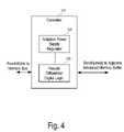
- FIG. 4shows a converter which can be used in a memory interface buffer according to one embodiment of the invention.
- a converter( 101 ) includes pseudo differential digital logic ( 105 ) that is used to implement a receiver and an adaptive power supply regulator ( 103 ) that is coupled to the pseudo differential digital logic to adaptively adjust the voltage supply to reduce power consumption and improve power supply noise performance.
- the pseudo differential digital logicis used at least in the receiving portion of a memory interface buffer for the serial link(s) to the adjacent advanced memory buffer.
- CMOS based pseudo differential logicto implement a high-speed data transceiver, which can be used in the memory interface buffer.
- one embodiment of the inventionfurther uses an adaptive power-supply regulator to adaptively adjust the power supply to the transceiver according to the working frequency, data transition pattern, fabrication process and working temperature variations.
- CMOS transistorsWhen the feature size of an integrated circuit is 0.18 um or larger, the power supply requirement of CMOS transistors is relatively high while the operating frequency of CMOS transistors is relatively low, in comparison with MOS transistors that are used to implement CML circuit. Thus, in such integrated circuits, a data transceiver using CML circuits can actually operate in relative high speed due to CML's low output voltage swing. Meanwhile, CML also produces less power-supply noise since it generates less current spikes related to the use of a near constant power supply current.
- CMLloses its advantage over CMOS logic in speed because the transconductance of the MOS transistors increases only slightly and eventually saturates with channel length reduction.
- increasing the power of CML circuits considerablycan increase the data transceiver's operating speed/frequency, such an approach can lead to the high power consumption of the transceiver.
- CMLmay not be suitable for use in high speed/frequency applications that requires lower power consumption.
- CMOS digital logicis preferred when the feature size of CMOS is reduced to 0.13 um or smaller.
- traditional CMOS logic circuit techniquehas the disadvantage of generating rather large current spikes, thus, higher power-supply noises.
- One embodiment of the inventionimplements CMOS pseudo differential logic circuits in the design of high-speed/frequency data transceivers, which increases the power-supply noises immunity of the transceiver while keeps the low-power advantage of CMOS logic circuits.
- CMOS logic circuitsconsume little power while not changing states; and the pseudo differential design of the logic circuit reduces the current spikes.
- an adaptive power-supply regulatoris further used to reduce power consumption of the transceiver as well as to reduce the power-supply noises.
- the CMOS based transceiveris used for high speed data transportation, such as in the memory interface buffer, in which the data transmission speed can be above one Gigabit per second.
- a transceiverhas substantially the same functional structure as the conventional transceiver, such as multiplexer, pre-driver, driver, data recovery, color recovery, de-multiplexer, etc.
- At least some of the MOS CML circuits used in the convectional transceiverare replaced with CMOS pseudo-different digital logic circuits.
- the output driveris still implemented using the CML circuit due to system requirement.
- only the output driver of the transceiveruses a MOS CML circuit.
- FIG. 5shows a block diagram example of a transceiver which can be used in a memory interface buffer according to one embodiment of the invention.
- the adaptive power supply regulator ( 201 )provides the voltage supply to the transceiver ( 203 ), which includes a multiplexer ( 231 ) to receive parallel input data, a pre-driver ( 233 ), a driver ( 235 ) of the interface, a pseudo differential digital logic circuit ( 241 ) to receive from the interface, a clock recovery ( 239 ), and data recovery & de-multiplexer ( 237 ) to send out parallel output data.
- the adaptive power supply regulatordoes not control the power supply of the drive ( 235 ).
- the pseudo differential digital logic circuit ( 241 )may cover more or less portion of the transceiver.
- the pseudo differential digital logic circuitmay be expanded to region ( 243 ) to implement a portion of the clock recovery ( 239 ) and a portion of data recovery & de-multiplexer ( 237 ).
- the pseudo differential digital logic circuitmay be further used in multiplexer ( 231 ) and/or the pre-driver ( 233 ).
- Pseudo differential digital logicuse two digital signal paths, which are complimentary, and a digital circuit (e.g., a latch) that is coupled in between the two digital signal paths to ensure that the output of the digital signal paths really have opposite polarity.
- a digital circuite.g., a latch
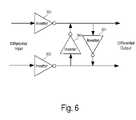
- FIGS. 6-9illustrate examples of a pseudo differential digital logic circuit which can be used in transceivers of memory interface buffers according to embodiments of the invention.
- a differential inputis converted into digital signals along two paths by inverters ( 301 and 303 ).
- Two inverters ( 305 and 307 )bridges between the outputs of the inverters ( 301 and 303 ) in opposite directions to ensure that the output of the inverters ( 301 and 303 ) really have opposite polarity for the differential output.
- the pseudo differential digital logicincludes a buffer ( 401 ) and an inverter ( 403 ) that converts a single-ended input into a pair of digital outputs along two paths.
- a common mode feedback logic block ( 405 )is used to take the output of the buffer ( 401 ) and the output of the inverter ( 403 ), generate a feedback to the buffer ( 401 ) and the inverter ( 403 ) according to the common mode detected in the outputs and uses the feedback to adjust the buffer ( 401 ) and inverter ( 403 ) to reduce and/or eliminate the common mode, so that the differential output of opposite polarity is generated.
- the differential outputcan be further elevated in magnitude using a pair of buffers or inverters (not shown in FIG. 7) along the two paths.
- the pseudo differential digital logicincludes two buffers ( 411 and 415 ) to generate a digital output along one path and an inventor ( 413 ) and a buffer ( 417 ) to generate another digital output along another path.
- a common mode feedback (CMFB) logic block ( 419 )is coupled to the output of the two path and the control of the buffers ( 415 and 417 ) to reduce and/or eliminate the common mode in a way similar as the common mode feedback (CMFB) logic block ( 405 ) in FIG. 7( a ).
- the CMFB block ( 419 )may control the buffer ( 411 ) and the inverter ( 413 ) to minimize the common mode.
- the buffer ( 417 )follows the inverter ( 413 ) on the path.
- a buffermay be placed before an inverter on the path.
- the pseudo differential digital logicincludes a buffer ( 501 ) and an inverter ( 503 ) that converts a single-ended input into a pair of digital outputs along two paths.
- a cross-coupled logic block ( 505 )is used to cross couple the output of the buffer ( 501 ) and the output of the inverter ( 503 ) so that the differential output of opposite polarity is generated.
- the cross couple logic block ( 505 )can be implemented using a pair of inverters connected in opposite direction, in a way as the inverters ( 305 and 307 ) in FIG. 3 .
- the differential outputcan be further elevated in magnitude using a pair of buffers or inverters (not shown in FIG. 8) along the two paths.
- the pseudo differential digital logicincludes two buffers ( 511 and 515 ) to generate a digital output along one path and an inventor ( 513 ) and a buffer ( 517 ) to generate another digital output along another path.
- a cross couple logic block ( 519 )is used to cross couple to the output of the two paths so that the outputs have opposite polarity in a way similar as the cross couple logic block ( 505 ) in FIG. 8( a ).
- the buffer ( 517 )follows the inverter ( 513 ) on the path.
- a buffermay be placed before an inverter on the path.
- the pseudo differential digital logicincludes two paths to generate two digital outputs and a clock synchronization logic block ( 605 ) is coupled between the two digital outputs to synchronize the clock of the digital outputs and generate the differential digital output.
- the clock synchronization logicincludes a phase detector and a voltage controlled oscillator (VCO).
- VCOvoltage controlled oscillator
- the clock synchronization logic block ( 605 )is used to recover clock from the input.
- a buffer ( 610 ) and an inverter ( 603 )are used along the two paths to generate the corresponding outputs that are the inputs to the clock synchronization circuit.
- a string of a combination of buffer(s) and/or inverter(s)can be used on each of the two paths to generate the differential output.
- CML circuitWhen the fabrication process scales down, the voltage supply of the transistors also comes down.
- the power consumption of CML circuitis proportional to VI, where V is the voltage supply and I is the operating (bias) current.
- the power consumption of CMOS PDL circuitis proportional to CV ⁇ 2f, where C is the loading capacitance, V is the voltage supply, and f is the operating frequency.
- the power consumption of CML circuitis a linear function of the voltage supply V while the power consumption of CMOS digital logic circuit is a square function of the voltage supply V, the power consumption of CMOS digital logic circuit scales down much faster than that of CML circuit as the voltage supply V scales down.
- CMOS PDL circuitconsumes less power than a CML circuit.
- the power consumption of a CML circuitis a function of voltage supply V and operating current 1 , but not a function of the operating frequency f.
- the power consumption of a CML circuitis independent of the nominal frequency of the signal and the data transfer pattern.
- a CML circuitryis typically designed to maintain full power and run at the highest possible frequency of the system for the data transfer performance.
- the power consumption of the CMOS PDL circuitis proportional to the operating frequency f.
- the operating frequency fWhen the operating frequency f is low, the circuitry consumes less power.
- no special coding (8B/10B)is used to maintain high transition rate and DC balance, it is highly possible that there is no transition for a long period of time in which the working frequency f is 0. Since the working frequency f changes from time to time, a CMOS PDL based circuit may consume less low power statistically.
- an adaptive power-supply regulatoris used to further reduce the power consumption of the transceiver.
- the power-supply regulatoradaptively adjusts the power supply of the transceiver according to the working frequency, data transition pattern, fabrication process and working temperature variations.
- the adaptive power-supply regulatornot only reduces power consumption of the transceiver but also functions as a power-supply filter to reduce the power-supply noises.
- the adaptive power-supply regulatorincludes a Phase-Locked Loop (PLL) and a bias generator.
- the Phase-Locked Loopincludes a phase detector (PD) ( 211 ), a loop filter (LF) ( 213 ), a voltage controlled oscillator (VCO) ( 217 ) and a frequency divider ( 215 ).
- the VCO of the Phase-Locked Loop (PLL) of the adaptive power-supply regulatoris the same as the VCO of the clock recovery of the transceiver.
- the VCOis implemented using CMOS logic circuits.
- the adaptive power-supply regulator and the transceivershare the same VCO.
- the working frequency of the VCO in the adaptive power-supply regulatoris designed to track the working frequency of the transceiver logic circuits (e.g., the highest working frequency) to optimize the power supply of the transceiver so that no extra power is wasted.
- the transceiveruses less power than a corresponding CML implementation.
- Phase-Locked Loop (PLL) in the adaptive power-supply regulatorcan be replaced with a Delay Locked Loop (DLL).
- PLLPhase-Locked Loop
- DLLDelay Locked Loop
- the adaptive power-supply regulatormay use a design known in the field.
- an adaptive power-supply regulator described by J. Kim and M. A. Horowitz in “Adaptive supply serial links with sub-1V operation and per-pin clock recovery, IEEE International Solid-State Circuits Conference, vol. XLV, pp. 268-269, February 2002,can be used with embodiments of the invention.
- a current mode logiccosts more die area than digital logic but has better noise performance.
- Digital logiccan achieve similar speed performance in deep-sub micron process.
- the power consumption of a digital logicis data pattern dependent, such that it consumes almost any power if there is no data activity.
- the current mode logicuses the same power regardless whether there is data activity or not.
- a general digital logichas bad noise performance.
- At least one embodiment of the inventionuses the pseudo-differential design and the regulated power supply to improve the noise performance.
- FIGS. 10-11illustrate examples of printed circuit boards according to embodiments of the invention.
- a printed circuit board ( 701 )includes a microprocessor (CPU) chip ( 703 ) (or a socket for the microprocessor) and traces to connect the microprocessor chip ( 703 ) to the northbridge chip ( 704 ), which is typically one of a chipset for the system core logic.
- the northbridge chip ( 704 )contains the memory controller ( 705 ), which is connected to the memory interface buffer ( 707 ) and further connected to FB-DIMMs (e.g., 709 , 711 , etc.)
- the memory interface buffer ( 707 )is installed directly on the printed circuit board ( 701 ).
- the memory interface buffer ( 707 )is installed on a module that has a form factor of a conventional memory module (e.g., an un-buffered or registered DIMMs), which can be inserted into the memory sockets for the conventional memory modules.
- a conventional memory modulee.g., an un-buffered or registered DIMMs
- the FB-DIMMsmay be connected to the memory interface buffer ( 707 ) via traces on the printed circuit board ( 701 ) (e.g., when the memory interface buffer is mounted directly on the printed circuit board), or be connected to the memory interface buffer ( 707 ) through serial cables. Multiple FB-DIMMs may be integrated in one unit, with a serial connection to the memory interface buffer ( 707 ).
- multiple memory interface bufferscan be coupled to the memory controller ( 705 ).
- a module containing the memory interface buffere.g., 707 or 717
- the printed circuit board ( 701 )can be installed on the printed circuit board ( 701 ) to allow the system to add more FB-DIMMs.
- a memory interface buffer chipmay include multiple interfaces to AMBs, such that multiple chains of FB-DIMMs may be connected to a memory interface buffer.
- a module containing the memory interface buffer and suitable for insertion into the conventional memory socketsmay also contain an AMB and memory chips, such that the memory interface and one FB-DIMM are integrated on one module insertable in a conventional memory socket for a parallel memory bus. Once such a module is inserted in the motherboard, further FB-DIMM can be chained after the AMB of the module.
- a module containing the memory interface buffermay include multiple interfaces to AMBs, such that multiple chains of FB-DIMMs may be connected to a module.
- the memory interface bufferis designed to be capable to communicate with Advanced Memory Buffer (AMB) according to a Joint Electron Device Engineering Council (JEDEC) specification.
- AMBAdvanced Memory Buffer
- JEDECJoint Electron Device Engineering Council
Landscapes
- Dram (AREA)
- Bus Control (AREA)
Abstract
Description
Claims (20)
Priority Applications (9)
| Application Number | Priority Date | Filing Date | Title |
|---|---|---|---|
| US11/277,650US7558124B2 (en) | 2005-11-16 | 2006-03-28 | Memory interface to bridge memory buses |
| CN2006100985371ACN1967708B (en) | 2005-11-16 | 2006-07-04 | Memory interface to bridge memory buses |
| US11/463,822US7577039B2 (en) | 2005-11-16 | 2006-08-10 | Memory interface to bridge memory buses |
| PCT/US2006/031537WO2007061467A2 (en) | 2005-11-16 | 2006-08-11 | Memory interface to bridge memory buses |
| PCT/US2006/034831WO2007061482A2 (en) | 2005-11-16 | 2006-09-08 | Memory interface to bridge memory buses |
| EP06803101AEP1949380A2 (en) | 2005-11-16 | 2006-09-08 | Memory interface to bridge memory buses |
| TW095138379ATW200723002A (en) | 2005-11-16 | 2006-10-18 | Memory interface to bridge memory buses |
| CN2006101451174ACN101000533B (en) | 2005-11-16 | 2006-11-13 | Memory interface for bridging memory bus |
| TW095142230ATW200741461A (en) | 2005-11-16 | 2006-11-15 | Memory interface to bridge memory buses |
Applications Claiming Priority (2)
| Application Number | Priority Date | Filing Date | Title |
|---|---|---|---|
| US11/281,211US7368950B2 (en) | 2005-11-16 | 2005-11-16 | High speed transceiver with low power consumption |
| US11/277,650US7558124B2 (en) | 2005-11-16 | 2006-03-28 | Memory interface to bridge memory buses |
Related Parent Applications (1)
| Application Number | Title | Priority Date | Filing Date |
|---|---|---|---|
| US11/281,211Continuation-In-PartUS7368950B2 (en) | 2005-11-16 | 2005-11-16 | High speed transceiver with low power consumption |
Related Child Applications (1)
| Application Number | Title | Priority Date | Filing Date |
|---|---|---|---|
| US11/281,211Continuation-In-PartUS7368950B2 (en) | 2005-11-16 | 2005-11-16 | High speed transceiver with low power consumption |
Publications (2)
| Publication Number | Publication Date |
|---|---|
| US20070121389A1 US20070121389A1 (en) | 2007-05-31 |
| US7558124B2true US7558124B2 (en) | 2009-07-07 |
Family
ID=38067683
Family Applications (1)
| Application Number | Title | Priority Date | Filing Date |
|---|---|---|---|
| US11/277,650Active2026-08-07US7558124B2 (en) | 2005-11-16 | 2006-03-28 | Memory interface to bridge memory buses |
Country Status (3)
| Country | Link |
|---|---|
| US (1) | US7558124B2 (en) |
| TW (1) | TW200723002A (en) |
| WO (1) | WO2007061467A2 (en) |
Cited By (15)
| Publication number | Priority date | Publication date | Assignee | Title |
|---|---|---|---|---|
| US20090063784A1 (en)* | 2007-08-31 | 2009-03-05 | Gower Kevin C | System for Enhancing the Memory Bandwidth Available Through a Memory Module |
| US20090063761A1 (en)* | 2007-08-31 | 2009-03-05 | Gower Kevin C | Buffered Memory Module Supporting Two Independent Memory Channels |
| US20090063729A1 (en)* | 2007-08-31 | 2009-03-05 | Gower Kevin C | System for Supporting Partial Cache Line Read Operations to a Memory Module to Reduce Read Data Traffic on a Memory Channel |
| US20090063785A1 (en)* | 2007-08-31 | 2009-03-05 | Gower Kevin C | Buffered Memory Module Supporting Double the Memory Device Data Width in the Same Physical Space as a Conventional Memory Module |
| US20090063787A1 (en)* | 2007-08-31 | 2009-03-05 | Gower Kevin C | Buffered Memory Module with Multiple Memory Device Data Interface Ports Supporting Double the Memory Capacity |
| US20090190429A1 (en)* | 2008-01-24 | 2009-07-30 | Brittain Mark A | System to Provide Memory System Power Reduction Without Reducing Overall Memory System Performance |
| US20090193200A1 (en)* | 2008-01-24 | 2009-07-30 | Brittain Mark A | System to Support a Full Asynchronous Interface within a Memory Hub Device |
| US20090190427A1 (en)* | 2008-01-24 | 2009-07-30 | Brittain Mark A | System to Enable a Memory Hub Device to Manage Thermal Conditions at a Memory Device Level Transparent to a Memory Controller |
| US20090193203A1 (en)* | 2008-01-24 | 2009-07-30 | Brittain Mark A | System to Reduce Latency by Running a Memory Channel Frequency Fully Asynchronous from a Memory Device Frequency |
| US20090193290A1 (en)* | 2008-01-24 | 2009-07-30 | Arimilli Ravi K | System and Method to Use Cache that is Embedded in a Memory Hub to Replace Failed Memory Cells in a Memory Subsystem |
| US20090193201A1 (en)* | 2008-01-24 | 2009-07-30 | Brittain Mark A | System to Increase the Overall Bandwidth of a Memory Channel By Allowing the Memory Channel to Operate at a Frequency Independent from a Memory Device Frequency |
| US8019919B2 (en) | 2007-09-05 | 2011-09-13 | International Business Machines Corporation | Method for enhancing the memory bandwidth available through a memory module |
| US8082482B2 (en) | 2007-08-31 | 2011-12-20 | International Business Machines Corporation | System for performing error correction operations in a memory hub device of a memory module |
| US8086936B2 (en) | 2007-08-31 | 2011-12-27 | International Business Machines Corporation | Performing error correction at a memory device level that is transparent to a memory channel |
| US8140936B2 (en) | 2008-01-24 | 2012-03-20 | International Business Machines Corporation | System for a combined error correction code and cyclic redundancy check code for a memory channel |
Families Citing this family (36)
| Publication number | Priority date | Publication date | Assignee | Title |
|---|---|---|---|---|
| US6471635B1 (en)* | 2000-02-10 | 2002-10-29 | Obtech Medical Ag | Anal incontinence disease treatment with controlled wireless energy supply |
| US6464628B1 (en)* | 1999-08-12 | 2002-10-15 | Obtech Medical Ag | Mechanical anal incontinence |
| ATE391468T1 (en) | 2000-02-10 | 2008-04-15 | Potencia Medical Ag | MECHANICAL DEVICE FOR IMPOTENCY TREATMENT |
| CA2635435C (en) | 2000-02-10 | 2010-05-25 | Potencia Medical Ag | Controlled urinary incontinence treatment |
| CA2396224C (en)* | 2000-02-11 | 2011-07-12 | Potencia Medical Ag | Controlled impotence treatment |
| WO2001047440A2 (en) | 2000-02-14 | 2001-07-05 | Potencia Medical Ag | Male impotence prosthesis apparatus with wireless energy supply |
| US7442165B2 (en)* | 2000-02-14 | 2008-10-28 | Obtech Medical Ag | Penile prosthesis |
| US7475187B2 (en)* | 2005-09-15 | 2009-01-06 | Infineon Technologies Ag | High-speed interface circuit for semiconductor memory chips and memory system including the same |
| DE102006025133A1 (en)* | 2006-05-30 | 2007-12-06 | Infineon Technologies Ag | Storage and storage communication system |
| US7379361B2 (en)* | 2006-07-24 | 2008-05-27 | Kingston Technology Corp. | Fully-buffered memory-module with redundant memory buffer in serializing advanced-memory buffer (AMB) for repairing DRAM |
| US7694031B2 (en)* | 2006-10-31 | 2010-04-06 | Globalfoundries Inc. | Memory controller including a dual-mode memory interconnect |
| US20080104352A1 (en)* | 2006-10-31 | 2008-05-01 | Advanced Micro Devices, Inc. | Memory system including a high-speed serial buffer |
| US7861140B2 (en)* | 2006-10-31 | 2010-12-28 | Globalfoundries Inc. | Memory system including asymmetric high-speed differential memory interconnect |
| US20080133864A1 (en)* | 2006-12-01 | 2008-06-05 | Jonathan Randall Hinkle | Apparatus, system, and method for caching fully buffered memory |
| US20080140907A1 (en)* | 2006-12-06 | 2008-06-12 | Dreps Daniel M | Multimodal Memory Controllers |
| US20080189457A1 (en)* | 2006-12-06 | 2008-08-07 | International Business Machines Corporation | Multimodal memory controllers |
| US20080155149A1 (en)* | 2006-12-20 | 2008-06-26 | De Araujo Daniel N | Multi-path redundant architecture for fault tolerant fully buffered dimms |
| EP2118760B1 (en)* | 2007-03-02 | 2012-02-22 | Rambus Inc. | A bi-directional interface circuit having a switchable current-source bias |
| WO2009096851A1 (en) | 2008-01-28 | 2009-08-06 | Milux Holding Sa | A drainage device comprising a filter cleaning device |
| MX2010008003A (en) | 2008-01-29 | 2010-09-24 | Milux Holding Sa | Apparatus for treating obesity. |
| WO2010042018A1 (en) | 2008-10-10 | 2010-04-15 | Milux Holding S.A. | Heart help device, system and method |
| AU2009302955B2 (en) | 2008-10-10 | 2017-01-05 | Implantica Patent Ltd. | Fastening means for implantable medical control assembly |
| WO2010042011A1 (en) | 2008-10-10 | 2010-04-15 | Milux Holding Sa | Heart help device, system, and method |
| US8874215B2 (en) | 2008-10-10 | 2014-10-28 | Peter Forsell | System, an apparatus, and a method for treating a sexual dysfunctional female patient |
| EP3851076A1 (en) | 2008-10-10 | 2021-07-21 | MedicalTree Patent Ltd. | An improved artificial valve |
| WO2010042046A1 (en) | 2008-10-10 | 2010-04-15 | Milux Holding S.A. | Apparatus, system and operation method for the treatment of female sexual dysfunction |
| US10952836B2 (en) | 2009-07-17 | 2021-03-23 | Peter Forsell | Vaginal operation method for the treatment of urinary incontinence in women |
| US9949812B2 (en) | 2009-07-17 | 2018-04-24 | Peter Forsell | Vaginal operation method for the treatment of anal incontinence in women |
| JP6054017B2 (en)* | 2011-07-13 | 2016-12-27 | ピーエスフォー ルクスコ エスエイアールエルPS4 Luxco S.a.r.l. | Semiconductor memory device |
| US9098209B2 (en) | 2011-08-24 | 2015-08-04 | Rambus Inc. | Communication via a memory interface |
| WO2013028859A1 (en)* | 2011-08-24 | 2013-02-28 | Rambus Inc. | Methods and systems for mapping a peripheral function onto a legacy memory interface |
| US11048410B2 (en) | 2011-08-24 | 2021-06-29 | Rambus Inc. | Distributed procedure execution and file systems on a memory interface |
| JP2013058277A (en)* | 2011-09-07 | 2013-03-28 | Renesas Electronics Corp | Semiconductor device |
| JP2015053095A (en)* | 2013-09-09 | 2015-03-19 | ソニー株式会社 | Memory, memory system, and memory control method |
| US9141541B2 (en) | 2013-09-20 | 2015-09-22 | Advanced Micro Devices, Inc. | Nested channel address interleaving |
| US10095421B2 (en) | 2016-10-21 | 2018-10-09 | Advanced Micro Devices, Inc. | Hybrid memory module bridge network and buffers |
Citations (17)
| Publication number | Priority date | Publication date | Assignee | Title |
|---|---|---|---|---|
| US5032744A (en) | 1989-10-31 | 1991-07-16 | Vlsi Technology, Inc. | High speed comparator with offset cancellation |
| US5430859A (en)* | 1991-07-26 | 1995-07-04 | Sundisk Corporation | Solid state memory system including plural memory chips and a serialized bus |
| US5977819A (en) | 1995-09-14 | 1999-11-02 | Ncr Corporation | CMOS gigabit serial link differential transmitter and receiver |
| US5990722A (en) | 1995-06-28 | 1999-11-23 | Sgs-Thomson Microelectronics S.A. | Short circuit protection of an audio/video data bus |
| US6157231A (en) | 1999-03-19 | 2000-12-05 | Credence System Corporation | Delay stabilization system for an integrated circuit |
| US6317352B1 (en) | 2000-09-18 | 2001-11-13 | Intel Corporation | Apparatus for implementing a buffered daisy chain connection between a memory controller and memory modules |
| US20040136411A1 (en) | 2003-01-10 | 2004-07-15 | Sierra Monolithics, Inc. | Highly integrated, high-speed, low-power serdes and systems |
| US6820163B1 (en)* | 2000-09-18 | 2004-11-16 | Intel Corporation | Buffering data transfer between a chipset and memory modules |
| US6830470B1 (en)* | 2003-06-20 | 2004-12-14 | Intel Corporation | Electrical device connector |
| US20050138267A1 (en)* | 2003-12-23 | 2005-06-23 | Bains Kuljit S. | Integral memory buffer and serial presence detect capability for fully-buffered memory modules |
| US20060095620A1 (en)* | 2004-10-29 | 2006-05-04 | International Business Machines Corporation | System, method and storage medium for merging bus data in a memory subsystem |
| US20060140317A1 (en) | 2002-11-28 | 2006-06-29 | Lorenzo Di Gregorio | Clock synchronization circuit |
| US20060195631A1 (en)* | 2005-01-31 | 2006-08-31 | Ramasubramanian Rajamani | Memory buffers for merging local data from memory modules |
| US7145359B2 (en) | 2004-06-28 | 2006-12-05 | Silicon Laboratories Inc. | Multiple signal format output buffer |
| US20070160053A1 (en)* | 2005-11-28 | 2007-07-12 | Coteus Paul W | Method and system for providing indeterminate read data latency in a memory system |
| US20080031030A1 (en)* | 2006-07-31 | 2008-02-07 | Metaram, Inc. | System and method for power management in memory systems |
| US20080052462A1 (en)* | 2006-08-24 | 2008-02-28 | Blakely Robert J | Buffered memory architecture |
- 2006
- 2006-03-28USUS11/277,650patent/US7558124B2/enactiveActive
- 2006-08-11WOPCT/US2006/031537patent/WO2007061467A2/enactiveApplication Filing
- 2006-10-18TWTW095138379Apatent/TW200723002A/enunknown
Patent Citations (18)
| Publication number | Priority date | Publication date | Assignee | Title |
|---|---|---|---|---|
| US5032744A (en) | 1989-10-31 | 1991-07-16 | Vlsi Technology, Inc. | High speed comparator with offset cancellation |
| US5430859A (en)* | 1991-07-26 | 1995-07-04 | Sundisk Corporation | Solid state memory system including plural memory chips and a serialized bus |
| US5990722A (en) | 1995-06-28 | 1999-11-23 | Sgs-Thomson Microelectronics S.A. | Short circuit protection of an audio/video data bus |
| US5977819A (en) | 1995-09-14 | 1999-11-02 | Ncr Corporation | CMOS gigabit serial link differential transmitter and receiver |
| US6157231A (en) | 1999-03-19 | 2000-12-05 | Credence System Corporation | Delay stabilization system for an integrated circuit |
| US6317352B1 (en) | 2000-09-18 | 2001-11-13 | Intel Corporation | Apparatus for implementing a buffered daisy chain connection between a memory controller and memory modules |
| US6820163B1 (en)* | 2000-09-18 | 2004-11-16 | Intel Corporation | Buffering data transfer between a chipset and memory modules |
| US20060140317A1 (en) | 2002-11-28 | 2006-06-29 | Lorenzo Di Gregorio | Clock synchronization circuit |
| US7180332B2 (en) | 2002-11-28 | 2007-02-20 | Infineon Technologies Ag | Clock synchronization circuit |
| US20040136411A1 (en) | 2003-01-10 | 2004-07-15 | Sierra Monolithics, Inc. | Highly integrated, high-speed, low-power serdes and systems |
| US6830470B1 (en)* | 2003-06-20 | 2004-12-14 | Intel Corporation | Electrical device connector |
| US20050138267A1 (en)* | 2003-12-23 | 2005-06-23 | Bains Kuljit S. | Integral memory buffer and serial presence detect capability for fully-buffered memory modules |
| US7145359B2 (en) | 2004-06-28 | 2006-12-05 | Silicon Laboratories Inc. | Multiple signal format output buffer |
| US20060095620A1 (en)* | 2004-10-29 | 2006-05-04 | International Business Machines Corporation | System, method and storage medium for merging bus data in a memory subsystem |
| US20060195631A1 (en)* | 2005-01-31 | 2006-08-31 | Ramasubramanian Rajamani | Memory buffers for merging local data from memory modules |
| US20070160053A1 (en)* | 2005-11-28 | 2007-07-12 | Coteus Paul W | Method and system for providing indeterminate read data latency in a memory system |
| US20080031030A1 (en)* | 2006-07-31 | 2008-02-07 | Metaram, Inc. | System and method for power management in memory systems |
| US20080052462A1 (en)* | 2006-08-24 | 2008-02-28 | Blakely Robert J | Buffered memory architecture |
Non-Patent Citations (8)
| Title |
|---|
| Fiedler et al., "A 1.0625Gbps Transceiver with 2x-Oversampling and Transmit Signal Pre-Emphasis," IEEE International Solid-State Circuits Conference, Published 1997, Session 15, pp. 238-239 and 464.* |
| JEDEC JESD205 Standard, "FBDIMM Specification: DDR2 SDRAM Fully Buffered DIMM (FBDIMM) Design Specification," Mar. 2007. pp. 1-129.* |
| JEDEC JESD82-20 Standard, "FBDIMM: Advanced Memory Buffer (AMB)," Mar. 2007. pp. 1-190.* |
| Kim et al., "Adaptive Supply Serial Links with Sub-1V Operation and Per-Pin Clock Recovery," IEEE International Solid-State Circuits Conference, Published 2002, Session 16, pp. 216-217 and 480.* |
| Kim et al., "Adaptive Supply Serial Links with Sub-1V Operation and Per-Pin Clock Recovery," IEEE Journal of Solid-State Circuits, Nov. 2002, vol. 37, No. 11, pp. 1403-1413.* |
| Rau et al., "Clock/Data Recovery PLL Using Half-Frequency Clock," IEEE Journal of Solid-State Circuits, Jul. 1997, vol. 32, No. 7, pp. 1156-1159.* |
| Sidiropoulos et al., "A Semidigital Dual Delay-Locked Loop," IEEE Journal of Solid-State Circuits, Nov. 1997, vol. 32, No. 11, pp. 1683-1692.* |
| Yuan et al., "New Single-Clock CMOS Latches and Flipflops with Improved Speed and Power Savings," IEEE Journal of Solid-State Circuits, Jan. 1997, vol. 32, No. 1, pp. 62-69.* |
Cited By (26)
| Publication number | Priority date | Publication date | Assignee | Title |
|---|---|---|---|---|
| US20090063784A1 (en)* | 2007-08-31 | 2009-03-05 | Gower Kevin C | System for Enhancing the Memory Bandwidth Available Through a Memory Module |
| US20090063761A1 (en)* | 2007-08-31 | 2009-03-05 | Gower Kevin C | Buffered Memory Module Supporting Two Independent Memory Channels |
| US20090063729A1 (en)* | 2007-08-31 | 2009-03-05 | Gower Kevin C | System for Supporting Partial Cache Line Read Operations to a Memory Module to Reduce Read Data Traffic on a Memory Channel |
| US20090063785A1 (en)* | 2007-08-31 | 2009-03-05 | Gower Kevin C | Buffered Memory Module Supporting Double the Memory Device Data Width in the Same Physical Space as a Conventional Memory Module |
| US20090063787A1 (en)* | 2007-08-31 | 2009-03-05 | Gower Kevin C | Buffered Memory Module with Multiple Memory Device Data Interface Ports Supporting Double the Memory Capacity |
| US8086936B2 (en) | 2007-08-31 | 2011-12-27 | International Business Machines Corporation | Performing error correction at a memory device level that is transparent to a memory channel |
| US7840748B2 (en) | 2007-08-31 | 2010-11-23 | International Business Machines Corporation | Buffered memory module with multiple memory device data interface ports supporting double the memory capacity |
| US8082482B2 (en) | 2007-08-31 | 2011-12-20 | International Business Machines Corporation | System for performing error correction operations in a memory hub device of a memory module |
| US7899983B2 (en) | 2007-08-31 | 2011-03-01 | International Business Machines Corporation | Buffered memory module supporting double the memory device data width in the same physical space as a conventional memory module |
| US7865674B2 (en)* | 2007-08-31 | 2011-01-04 | International Business Machines Corporation | System for enhancing the memory bandwidth available through a memory module |
| US7861014B2 (en) | 2007-08-31 | 2010-12-28 | International Business Machines Corporation | System for supporting partial cache line read operations to a memory module to reduce read data traffic on a memory channel |
| US7818497B2 (en) | 2007-08-31 | 2010-10-19 | International Business Machines Corporation | Buffered memory module supporting two independent memory channels |
| US8019919B2 (en) | 2007-09-05 | 2011-09-13 | International Business Machines Corporation | Method for enhancing the memory bandwidth available through a memory module |
| US20090193200A1 (en)* | 2008-01-24 | 2009-07-30 | Brittain Mark A | System to Support a Full Asynchronous Interface within a Memory Hub Device |
| US7770077B2 (en) | 2008-01-24 | 2010-08-03 | International Business Machines Corporation | Using cache that is embedded in a memory hub to replace failed memory cells in a memory subsystem |
| US20090193201A1 (en)* | 2008-01-24 | 2009-07-30 | Brittain Mark A | System to Increase the Overall Bandwidth of a Memory Channel By Allowing the Memory Channel to Operate at a Frequency Independent from a Memory Device Frequency |
| US20090193290A1 (en)* | 2008-01-24 | 2009-07-30 | Arimilli Ravi K | System and Method to Use Cache that is Embedded in a Memory Hub to Replace Failed Memory Cells in a Memory Subsystem |
| US7925825B2 (en) | 2008-01-24 | 2011-04-12 | International Business Machines Corporation | System to support a full asynchronous interface within a memory hub device |
| US7925826B2 (en) | 2008-01-24 | 2011-04-12 | International Business Machines Corporation | System to increase the overall bandwidth of a memory channel by allowing the memory channel to operate at a frequency independent from a memory device frequency |
| US7925824B2 (en) | 2008-01-24 | 2011-04-12 | International Business Machines Corporation | System to reduce latency by running a memory channel frequency fully asynchronous from a memory device frequency |
| US7930469B2 (en) | 2008-01-24 | 2011-04-19 | International Business Machines Corporation | System to provide memory system power reduction without reducing overall memory system performance |
| US7930470B2 (en) | 2008-01-24 | 2011-04-19 | International Business Machines Corporation | System to enable a memory hub device to manage thermal conditions at a memory device level transparent to a memory controller |
| US20090193203A1 (en)* | 2008-01-24 | 2009-07-30 | Brittain Mark A | System to Reduce Latency by Running a Memory Channel Frequency Fully Asynchronous from a Memory Device Frequency |
| US20090190427A1 (en)* | 2008-01-24 | 2009-07-30 | Brittain Mark A | System to Enable a Memory Hub Device to Manage Thermal Conditions at a Memory Device Level Transparent to a Memory Controller |
| US20090190429A1 (en)* | 2008-01-24 | 2009-07-30 | Brittain Mark A | System to Provide Memory System Power Reduction Without Reducing Overall Memory System Performance |
| US8140936B2 (en) | 2008-01-24 | 2012-03-20 | International Business Machines Corporation | System for a combined error correction code and cyclic redundancy check code for a memory channel |
Also Published As
| Publication number | Publication date |
|---|---|
| WO2007061467A2 (en) | 2007-05-31 |
| TW200723002A (en) | 2007-06-16 |
| US20070121389A1 (en) | 2007-05-31 |
| WO2007061467A3 (en) | 2009-04-30 |
Similar Documents
| Publication | Publication Date | Title |
|---|---|---|
| US7558124B2 (en) | Memory interface to bridge memory buses | |
| US7577039B2 (en) | Memory interface to bridge memory buses | |
| US7368950B2 (en) | High speed transceiver with low power consumption | |
| US11317510B2 (en) | Load reduced memory module | |
| US6496445B2 (en) | Semiconductor memory device having altered clock frequency for address and/or command signals, and memory module and system having the same | |
| US7111108B2 (en) | Memory system having a multiplexed high-speed channel | |
| US7161820B2 (en) | Memory module and memory system having an expandable signal transmission, increased signal transmission and/or high capacity memory | |
| JP2005228458A (en) | On die termination mode transfer circuit in semiconductor memory device and its method | |
| JP2008165790A (en) | Modular memory controller clocking architecture | |
| KR100560644B1 (en) | Integrated circuit device having a clock synchronizing circuit | |
| US10241538B2 (en) | Resynchronization of a clock associated with each data bit in a double data rate memory system | |
| US7558980B2 (en) | Systems and methods for the distribution of differential clock signals to a plurality of low impedance receivers | |
| KR20230160043A (en) | Semiconductor apparatus performing a plurality of clock signaling and semiconductor system including the same | |
| HK1106308A (en) | Memory interface to bridge memory buses | |
| Eble et al. | Power-efficient I/O design considerations for high-bandwidth applications | |
| JP2002109888A (en) | Semiconductor integrated circuit device | |
| Beers et al. | A novel memory bus driver/receiver architecture for higher throughput | |
| HK1106318A (en) | Memory interface to bridge memory buses | |
| US20040057330A1 (en) | Circuit topology for clock signal distribution topology | |
| CN120124573A (en) | Clock driver chip, press-fit memory module and information processing system | |
| HK1106319A (en) | High speed transceiver with low power consumption | |
| GB2379542A (en) | System comprising a memory module | |
| Gauthier et al. | Dynamic receiver biasing for inter-chip communication |
Legal Events
| Date | Code | Title | Description |
|---|---|---|---|
| AS | Assignment | Owner name:MONTAGE TECHNOLOGY GROUP, LTD., VIRGIN ISLANDS, BR Free format text:ASSIGNMENT OF ASSIGNORS INTEREST;ASSIGNORS:WU, LARRY LEI;SHAN, GANG;GUO, ZHENG-DONG;AND OTHERS;REEL/FRAME:017709/0698;SIGNING DATES FROM 20060524 TO 20060601 | |
| STCF | Information on status: patent grant | Free format text:PATENTED CASE | |
| FEPP | Fee payment procedure | Free format text:PAT HOLDER CLAIMS SMALL ENTITY STATUS, ENTITY STATUS SET TO SMALL (ORIGINAL EVENT CODE: LTOS); ENTITY STATUS OF PATENT OWNER: SMALL ENTITY | |
| FPAY | Fee payment | Year of fee payment:4 | |
| AS | Assignment | Owner name:MONTAGE TECHNOLOGY GROUP LIMITED, CAYMAN ISLANDS Free format text:CONTINUATION;ASSIGNOR:MONTAGE TECHNOLOGY GROUP LIMITED;REEL/FRAME:036026/0192 Effective date:20060424 | |
| AS | Assignment | Owner name:MONTAGE TECHNOLOGY HOLDINGS COMPANY LIMITED, CAYMA Free format text:ASSIGNMENT OF ASSIGNORS INTEREST;ASSIGNOR:MONTAGE TECHNOLOGY GROUP LIMITED;REEL/FRAME:036213/0491 Effective date:20150728 | |
| FEPP | Fee payment procedure | Free format text:PAT HOLDER NO LONGER CLAIMS SMALL ENTITY STATUS, ENTITY STATUS SET TO UNDISCOUNTED (ORIGINAL EVENT CODE: STOL); ENTITY STATUS OF PATENT OWNER: SMALL ENTITY | |
| FPAY | Fee payment | Year of fee payment:8 | |
| FEPP | Fee payment procedure | Free format text:PAYOR NUMBER ASSIGNED (ORIGINAL EVENT CODE: ASPN); ENTITY STATUS OF PATENT OWNER: SMALL ENTITY | |
| FEPP | Fee payment procedure | Free format text:ENTITY STATUS SET TO SMALL (ORIGINAL EVENT CODE: SMAL); ENTITY STATUS OF PATENT OWNER: SMALL ENTITY | |
| MAFP | Maintenance fee payment | Free format text:PAYMENT OF MAINTENANCE FEE, 12TH YR, SMALL ENTITY (ORIGINAL EVENT CODE: M2553); ENTITY STATUS OF PATENT OWNER: SMALL ENTITY Year of fee payment:12 |