US7558109B2 - Nonvolatile memory with variable read threshold - Google Patents
Nonvolatile memory with variable read thresholdDownload PDFInfo
- Publication number
- US7558109B2 US7558109B2US11/556,626US55662606AUS7558109B2US 7558109 B2US7558109 B2US 7558109B2US 55662606 AUS55662606 AUS 55662606AUS 7558109 B2US7558109 B2US 7558109B2
- Authority
- US
- United States
- Prior art keywords
- voltages
- memory
- flash memory
- memory system
- threshold voltage
- Prior art date
- Legal status (The legal status is an assumption and is not a legal conclusion. Google has not performed a legal analysis and makes no representation as to the accuracy of the status listed.)
- Active, expires
Links
Images


Classifications
- G—PHYSICS
- G11—INFORMATION STORAGE
- G11C—STATIC STORES
- G11C11/00—Digital stores characterised by the use of particular electric or magnetic storage elements; Storage elements therefor
- G11C11/56—Digital stores characterised by the use of particular electric or magnetic storage elements; Storage elements therefor using storage elements with more than two stable states represented by steps, e.g. of voltage, current, phase, frequency
- G11C11/5621—Digital stores characterised by the use of particular electric or magnetic storage elements; Storage elements therefor using storage elements with more than two stable states represented by steps, e.g. of voltage, current, phase, frequency using charge storage in a floating gate
- G11C11/5642—Sensing or reading circuits; Data output circuits
- G—PHYSICS
- G06—COMPUTING OR CALCULATING; COUNTING
- G06F—ELECTRIC DIGITAL DATA PROCESSING
- G06F11/00—Error detection; Error correction; Monitoring
- G06F11/07—Responding to the occurrence of a fault, e.g. fault tolerance
- G06F11/08—Error detection or correction by redundancy in data representation, e.g. by using checking codes
- G06F11/10—Adding special bits or symbols to the coded information, e.g. parity check, casting out 9's or 11's
- G06F11/1008—Adding special bits or symbols to the coded information, e.g. parity check, casting out 9's or 11's in individual solid state devices
- G06F11/1072—Adding special bits or symbols to the coded information, e.g. parity check, casting out 9's or 11's in individual solid state devices in multilevel memories
- G—PHYSICS
- G11—INFORMATION STORAGE
- G11C—STATIC STORES
- G11C16/00—Erasable programmable read-only memories
- G11C16/02—Erasable programmable read-only memories electrically programmable
- G11C16/06—Auxiliary circuits, e.g. for writing into memory
- G11C16/26—Sensing or reading circuits; Data output circuits
- G—PHYSICS
- G11—INFORMATION STORAGE
- G11C—STATIC STORES
- G11C16/00—Erasable programmable read-only memories
- G11C16/02—Erasable programmable read-only memories electrically programmable
- G11C16/06—Auxiliary circuits, e.g. for writing into memory
- G11C16/34—Determination of programming status, e.g. threshold voltage, overprogramming or underprogramming, retention
- G11C16/349—Arrangements for evaluating degradation, retention or wearout, e.g. by counting erase cycles
Definitions
- This inventionrelates to nonvolatile memory systems and to methods of operating nonvolatile memory systems.
- Nonvolatile memory systemsare used in various applications. Some nonvolatile memory systems are embedded in a larger system such as a personal computer. Other nonvolatile memory systems are removably connected to a host system and may be interchanged between different host systems. Examples of such removable memory systems include memory cards and USB flash drives. Electronic circuit cards, including non-volatile memory cards, have been commercially implemented according to a number of well-known standards. Memory cards are used with personal computers, cellular telephones, personal digital assistants (PDAs), digital still cameras, digital movie cameras, portable audio players and other host electronic devices for the storage of large amounts of data.
- PDAspersonal digital assistants
- Such cardsusually contain a re-programmable non-volatile semiconductor memory cell array along with a controller that controls and supports operation of the memory cell array and interfaces with a host to which the card is connected.
- a controllerthat controls and supports operation of the memory cell array and interfaces with a host to which the card is connected.
- Several of the same type of cardmay be interchanged in a host card slot designed to accept that type of card.
- a card made according to one standardis usually not useable with a host designed to operate with a card of another standard.
- Memory card standardsinclude PC Card, CompactFlashTM card (CFTM card), SmartMediaTM card, MultiMediaCard (MMCTM), Secure Digital (SD) card, a miniSDTM card, Subscriber Identity Module (SIM), Memory StickTM, Memory Stick Duo card and microSD/TransFlashTM memory module standards.
- USB flash drive productscommercially available from SanDisk Corporation under its trademark “Cruzer®.” USB flash drives are typically larger and shaped differently than the memory cards described above.
- Data stored in a nonvolatile memory systemmay contain erroneous bits when data is read.
- Traditional ways to reconstruct corrupted datainclude the application of Error Correction Codes (ECCs).
- ECCsError Correction Codes
- Simple Error Correction Codesencode data by storing additional parity bits, which set the parity of groups of bits to a required logical value, when the data is written into the memory system. If during storage the data is erroneous, the parity of groups of bits may change. Upon reading the data from the memory system, the parity of the group of the bits is computed once again by the ECC. Because of the data corruption the computed parity may not match the required parity condition, and the ECC may detect the corruption.
- ECCscan have at least two functions: error detection and error correction. Capability for each of these functions is typically measured in the number of bits that can be detected as erroneous and subsequently corrected. Detection capability can be the same or greater than the correction capability. A typical ECC can detect a higher number of error bits than it can correct. A collection of data bits and parity bits is sometimes called a word.
- An early exampleis the (7,4) Hamming code, which has the capability of detecting up to two errors per word (seven bits in this example) and has the capability of correcting one error in the seven-bit word.
- More sophisticated ECCscan correct more than a single error per word, but it becomes computationally increasingly complex to reconstruct the data.
- Common practiceis to recover the data with some acceptably small likelihood of incorrect recovery.
- the probability of reliable data recoveryalso decreases rapidly or the associated costs in additional hardware and/or performance become prohibitively high.
- datacan be represented by the threshold voltages of transistors.
- different digital data storage valuescorrespond to different voltage ranges. If, for some reason, during the read operation the voltage levels shift from their preferred ranges, an error occurs. The error may be detected by the ECC and in some cases these errors may be corrected.
- a plurality of memory statesare mapped to a first threshold window, where individual ones of the plurality of memory cells are mapped to sub-ranges of the first threshold window, at a subsequent second time, the plurality of memory states are mapped to a second threshold window, where individual ones of the plurality of memory states are mapped to sub-ranges of the second threshold window, the second threshold window being wider than the first threshold window.
- a method of reading data from a flash memory arrayincludes reading first data bits from the memory by comparing threshold voltages of a plurality of memory cells to first predetermined voltages, decoding the first data bits in an ECC decoder, and subsequently reading second data bits from the plurality of memory cells by comparing threshold voltages of memory cells to second predetermined voltages, the second predetermined voltages determined from the decoding of the first data bits in the ECC decoder.
- a flash memory systemcomprises a flash memory array that includes a plurality of cells programmed to a plurality of programmed states; and a reading circuit connected to the memory array, the reading circuit comparing a memory cell threshold voltage to a first plurality of predetermined voltages do distinguish the plurality of programmed states in a first mode and comparing the memory cell threshold voltage to a second plurality of predetermined voltages to distinguish the plurality of programmed states in a second mode, the highest one of the second plurality of predetermined voltages being higher than the highest one of the first plurality of predetermined voltages.
- a flash memory systemcomprises a memory array that includes a plurality of nonvolatile memory cells; an ECC decoder that decodes data from the memory array; a reading circuit connected to the memory array, the reading circuit comparing a threshold voltage of a memory cell to at least one predetermined voltage to determine a programmed state of the memory cell; and an adjustment circuit that increases or decreases the at least one predetermined voltage in response to information from the ECC decoder.
- FIG. 1shows likelihood functions of threshold voltages of cells programmed to a logic 1 state and a logic 0 state in a nonvolatile memory, including a voltage V D used to discriminate logic 1 and logic 0 states.
- FIG. 2shows components of a memory system including a memory array, modulator/demodulator circuits and encoder/decoder circuits.
- FIG. 3shows likelihood function of read threshold voltages of cells programmed to a logic 1 state and a logic 0 state, showing threshold voltage values.
- FIG. 4shows components of a memory system including a memory array, modulator/demodulator circuits and encoder/decoder circuits, a demodulator providing likelihood values to a decoder.
- FIG. 5shows an ECC unit having a Soft-Input Soft-Output (SISO) decoder.
- SISOSoft-Input Soft-Output
- FIG. 6shows likelihood functions of a logic 1 state and a logic 0 state of a memory cell with two exemplary discrimination voltages.
- FIG. 7Ashows likelihood functions of eight memory states, representing three bits of data, with three read passes providing discrimination between memory states and additional resolution within memory states.
- FIG. 7Bshows an exemplary arrangement of read voltages including a discrimination voltage and additional read voltages at increments on either side of the discrimination voltage.
- FIG. 8shows how a likelihood function for a memory cell state may change as the memory is used, the likelihood distribution becoming wider with use.
- FIG. 9Ashows likelihood functions of four memory states and discrimination voltages resolving those states at an early stage of memory life.
- FIG. 9Bshows likelihood functions of the four memory states of FIG. 9A at a later stage of memory life with the same discrimination voltages.
- FIG. 10Ashows likelihood functions of four memory states at an early stage of memory life according to another embodiment where discrimination voltages are more closely spaced than in the previous example.
- FIG. 10Bshows likelihood functions of the four memory states of FIG. 10A at a later stage of memory life with adjusted discrimination voltages that are more widely spaced than discrimination voltages of FIG. 10A .
- FIG. 11shows a memory system including an ECC decoder, a statistical unit that gathers statistical information regarding corrections by the ECC decoder and an adjustment unit that adjusts operating parameters such as read voltages or programming target voltages in response to a signal from the statistical unit.
- FIG. 1shows the relationship between a physical parameter indicating a memory cell state (threshold voltage, V T ) and the logical values to which the memory cell may be programmed.
- V Tthreshold voltage
- the cellstores one bit of data.
- Cells programmed to the logic 0 stategenerally have a higher threshold voltage than cells in the logic 1 (unprogrammed) state.
- the logic 1 stateis the unprogrammed state of the memory cell.
- a first likelihood functionis shown for cells programmed to logic 1 and a second for cells programmed to logic 0. However, these functions have some degree of overlap between them.
- a discrimination voltage V Dis used in reading such cells. Cells having a threshold voltage below V D are considered to be in state 1, while those having a threshold voltage above V D are considered to be in state 0. As FIG. 1 shows, this may not always be correct. Because of the overlap between functions, there is a non-zero likelihood that a memory cell programmed to a logic 1 state will be read as having a threshold voltage greater than V D and so will be read as being in a logic 0 state. Similarly, there is a non-zero likelihood that a memory cell programmed to a logic 0 state will be read as having a logic 1 state.
- Overlap between functionsoccurs for a number of reasons including physical defects in the memory array and disturbance caused to programmed cells by later programming or reading operations in the memory array. Overlap may also occur due to a general lack of ability to keep a large number of cells within a very tight threshold voltage range. Certain programming techniques may allow functions of threshold voltages to be narrowed (have smaller standard deviations). However, such programming may take more time. In some memory systems, more than one bit is stored in a memory cell. In general, it is desirable to store as many bits as possible in a memory cell. In order to efficiently use the available threshold voltage range, functions for adjacent states may be such that they significantly overlap.
- Nonvolatile memory systemscommonly employ ECC methods to overcome errors that occur in data that is read from a memory array. Such methods generally calculate some additional ECC bits from input data to be stored in a memory array according to an encoding system. Other ECC schemes may map input data to output data in a more complex way. The ECC bits are generally stored along with the input data but may be stored separately. The input data and ECC bits are later read from the nonvolatile memory array together and a decoder uses both the data and ECC bits to check if any errors are present. In some cases, such ECC bits may also be used to identify a bit that is in error.
- ECC bitsto data bits is not the only way to encode data before storing it in a nonvolatile memory.
- data bitsmay be encoded according to a scheme that provides the following transformations: 00 to 1111, 01 to 1100, 10 to 0011 and 11 to 0000.
- FIG. 2shows an example of input data being stored in a memory system 200 .
- Input datais first received by an ECC unit 201 that includes an encoder 203 .
- the input datamay be host data to be stored in memory system 200 or may be data generated by a memory controller.
- the example of FIG. 2shows four input data bits 1001 .
- Encoder 203then calculates ECC bits ( 1111 ) from the input data bits using an encoding scheme.
- One example of an encoding schemeis to generate ECC bits that are parity bits for selected groups of data bits.
- Modulator 207converts the digital data sent by ECC unit 201 to a form in which it is written in a memory array 209 .
- the digital datais converted to a plurality of threshold voltage values in a plurality of memory cells.
- various circuits used to convert digital data to a stored threshold voltage in a memory cellmay be considered to form a modulator.
- each memory cellmay hold one bit of data.
- each memory cellmay have a threshold voltage in one of two ranges, one signifying a logic “1” state and the other signifying a logic “0” state as shown in FIG.
- the memory cells storing a logic “1” statehave a threshold voltage that is less than V D ( ⁇ V D ) while the memory cells storing a logic “0” state have a threshold voltage that is greater than V D (>V D ).
- Cellsmay be programmed and verified to a nominal threshold voltage higher than V D to ensure that, at least initially, there is some preferred separation between cells programmed to the two logic states.
- Datamay be stored in memory array 209 for some period of time. During this time, various events may occur to cause threshold voltages of memory cells to change. In particular, operations involving programming and reading may require voltages to be applied to word lines and bit lines in a manner that affects other previously programmed cells. Such disturbs are particularly common where dimensions of devices are reduced so that the interaction between adjacent cells is significant. Charge may also be lost over long periods of time. Such data retention failures can also cause data to change when read. As a result of such changes, data bits may be read out having different states than the data bits originally programmed. In the example of FIG. 2 , one input data bit 211 is read as having a threshold value less than V D ( ⁇ V D ) when it was originally written having a threshold value greater than V D (>V D ).
- the threshold voltages of memory cellsare converted to bits of data by a demodulator 213 in modulation/demodulation unit 205 .
- Demodulator 213may include sense amplifiers that read a voltage or current from a memory cell in memory array 209 and derive the state of the cell from the reading.
- a memory cell having a threshold voltage less than V Dgives a demodulated output of “1”
- a memory cell having a threshold voltage that is greater than V D (>V D )gives a demodulated output of “0.”
- the second bit 208 of this sequenceis in error as a result of being stored in the memory array 209 .
- Decoder 215determines from data bits and ECC bits if there are any errors. If a small number of errors is present that is within the correction capability of the code, the errors are corrected. If large numbers of errors are present, they may be identified but not corrected if they are within the detection capability of the code. If the number of errors exceeds the detection capability of the code, the errors may not be detected, or may result in an erroneous correction. In the example of FIG. 2 , the error in the second bit is detected and is corrected. This provides an output ( 1001 ) from decoder 215 that is identical to the input sequence.
- decoding of memory system 200is considered to be hard-input hard-output decoding because decoder 215 receives only data bits representing input data bits and ECC bits, and decoder 215 outputs a corrected sequence of data bits corresponding to input data bits (or fails to give an output if the number of errors is too high).
- FIG. 4shows a memory system 421 using a data storage process that is similar to that of memory system 200 (using the same input data bits and ECC bits) with a different read process.
- memory system 421instead of simply determining whether a threshold voltage is above or below a particular value, memory system 421 reads threshold voltages as shown in FIG. 3 . It will be understood that actual threshold voltage is not necessarily read. Other means of cell operation may be used to store and retrieve data (e.g. current sensing). Voltage sensing is merely used as an example. Generally, threshold voltage refers to a gate voltage at which a transistor turns on.
- FIG. 4shows a read occurring that provides more detailed information than the previous example. This may be considered a read with a higher resolution than that of FIG.
- the readings corresponding to the second and third bitsare in error.
- the raw voltages read from memory array 423 of FIG. 4 by a series of read operationsare sent to a demodulator 425 in a modulation/demodulation unit 427 .
- the raw voltageshave a finite resolution dictated by the resolution of the Analog-to-Digital conversion.
- raw datais converted into likelihood data.
- each cell readingis converted into a likelihood that the corresponding bit is a one or a zero.
- the series of readings from the memory array(0.75, 0.05, 0.10, 0.15, 1.25, 1.0, 3.0, and 0.5 volts) can indicate not only the state of the cell, but can also be used to provide a degree of certainty as to that state.
- Thismay be expressed as a likelihood that a memory cell was programmed with a particular bit. Thus, readings that are close to 0 volts may give low likelihood values, while readings that are farther from 0 volts give higher likelihood values.
- the likelihood values shownare log likelihood ratios (explained in detail below). This provides negative numbers for cells in a logic 0 state and positive numbers for cells in a logic 1 state, with the magnitude of the number indicating the likelihood that the state is correctly identified.
- the second and third likelihood values(0.1, 0.2) indicate logic “1”. The second and third values indicate likelihoods that are quite low.
- Likelihood valuesare sent to a decoder 429 in an ECC unit 431 (in some cases, obtaining likelihood values from raw values may be considered as being performed in the decoder).
- ECC unit 431also includes encoder 432 .
- the decoder 429performs decoding operations on likelihood values.
- Such a decodermay be considered a soft-input decoder.
- soft-inputrefers to an input that includes some quality information related to data that are to be decoded. The additional information provided as a soft-input generally allows a decoder to obtain better results.
- a decodermay perform decoding calculations using a soft-input to provide calculated likelihood values as an output.
- SISOSoft-Input Soft-Output
- a SISO decodermay form part of a larger decoder that provides a hard output to another unit. SISO decoders generally provide good performance and in some cases may provide better performance than is possible with hard-input hard-output decoding. In particular, for the same amount of overhead (number of ECC bits) a SISO decoder may provide greater error correction capability.
- a suitable encoding/decoding schememay be implemented and demodulation is adapted to efficiently obtain a soft-input without excessive complexity and without requiring excessive time for reading data from the memory array.
- a soft-input for a SISO decoderis provided by reading data in a nonvolatile memory array with a resolution that resolves a larger number of states than were used in programming the memory.
- datamay be written by programming a memory cell to one of two threshold voltage ranges and subsequently read by resolving three or more threshold voltage ranges.
- the number of threshold voltage ranges used in readingwill be some multiple of the number of threshold voltage ranges used in programming (for example, twice as many). However, this is not always the case.
- An ECC unitmay be formed as a dedicated circuit or this function may be performed by firmware in a controller.
- a controlleris an Application Specific Integrated Circuit (ASIC) that has circuits designed for specific functions such as ECC and also has firmware to manage controller operations.
- ASICApplication Specific Integrated Circuit
- an encoder/decodermay be formed by a combination of hardware and firmware in the memory controller.
- An encoder/decoder (ECC unit)may alternatively be located on the memory chip.
- the modulation/demodulation unitmay be on a memory chip, on a controller chip, on a separate chip or some combination.
- a modulation/demodulation unitwill include at least some components on the memory chip (such as peripheral circuits connected to a memory array). While FIG. 4 indicates threshold voltages being read to a high resolution (an analog read), the degree of resolution chosen may depend on a number of factors including the type of nonvolatile memory used.
- FIG. 5shows a more detailed view of ECC unit 431 , particularly decoder 429 .
- Decoder 429includes a SISO decoder 532 and a soft-hard converter 534 .
- SISO decodersgenerally accept raw likelihood data and perform ECC calculations on the raw likelihood data to provide calculated likelihood data.
- the calculated likelihood datamay be considered a soft-output.
- such a soft-outputis then provided as an input to the SISO decoder so that a second decoding iteration is performed.
- a SISO decodermay perform successive iterations until at least one predetermined condition is achieved. For example, a predetermined condition may be that all bits have a likelihood that is greater than a certain minimum value.
- a predetermined conditioncould also be an aggregate of likelihood values such as a mean likelihood value.
- a predetermined conditionmay be convergence of results from one iteration to the next (i.e. keep iterating until there is little improvement from additional iterations).
- a predetermined conditionmay be that a predetermined number of iterations are completed. Combinations of these conditions may also be used.
- Decodingis performed using an encoded pattern in the data that is the result of encoding performed by encoder 432 on the data before it was stored. Encoder 432 and decoder 429 are both considered parts of ECC unit 431 .
- Efficient decodingdepends on having a suitable encoding/decoding scheme.
- Various schemesare known for encoding data in a manner that is suitable for subsequent decoding in a SISO decoder such as SISO decoder 532 .
- Encoding/decoding schemesinclude, but are not limited to, turbo codes, product codes, BCH codes, Reed-Solomon codes, convolutional codes (see U.S. patent application Ser. Nos. 11/383,401 and 11/383,405), Hamming codes, and Low Density Parity Check (LDPC) codes.
- LDPCLow Density Parity Check
- FIG. 6shows likelihood functions 635 a , 635 b for read threshold voltages of cells programmed to logic 1 and programmed to logic 0.
- a first discrimination voltage V Dis shown at a location that provides a large number of errors because any cell having a threshold voltage higher than V D is considered to be programmed to logic 0, even though as FIG. 6 shows, there is a significant likelihood that such a cell was in fact programmed to logic 1.
- V Das a discrimination voltage means that a significant number of cells are read as being in logic 0 though they were programmed to logic 1.
- Such data bitsare generally corrected by ECC. There is a very low likelihood that a cell programmed to logic 0 will be read as having logic 1, so ECC correction of such bits is rare. Thus, an ECC decoder in this case would perform more 0-to-1 corrections than 1-to-0 corrections.
- a second discrimination voltage V D ′is shown at a threshold voltage where the logic 1 function and the logic 0 function intersect.
- V D ′threshold voltage of V D ′
- the discrimination voltage at V D ′there is some likelihood that a cell's threshold voltage will indicate the wrong logic state.
- the likelihoodis low and the number of cells programmed to logic 0 that are subsequently read as having logic 1 is equal to the number of cells programmed to logic 1 that are subsequently read as having logic 0.
- a discrimination voltageis not at its optimum value (e.g.
- V Dit may be desirable to adjust the discrimination voltage to bring it to its optimum (e.g. V D ′), or at least bring it closer to its optimum value.
- One way to detect that a discrimination voltage is not at its optimum valueis from correction made by an ECC decoder to bits corresponding to memory states on either side of the discrimination voltage.
- An ECC decodingcan generally indicate whether a discrimination voltage is located at an optimum location from the number of corrections made between logic states on either side of the discrimination. If a discrimination voltage is not at its optimum location, the ECC decoding may indicate (from the number of corrections from states on either side of the discrimination voltage) the direction in which the discrimination voltage should be moved. ECC decoding may also indicate how much a discrimination voltage should be moved from the respective numbers of corrections from the higher state (logic 0 in this example) to the lower state (logic 1 in this example) compared to corrections from the lower state to the higher state. Suitable circuits may be used to determine, from ECC corrections of data read using initial discrimination voltages, whether discrimination voltages should be adjusted. If such adjustments are to be made then the circuits may indicate in which direction they should be adjusted and may also indicate by how much they should be adjusted.
- FIG. 6only shows two programmed states representing one bit of stored data
- memory cellsmay be programmed to three or more states representing more than one bit of stored data.
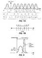
- FIG. 7Ashows an example where a threshold voltage range of a memory cell (threshold window) is divided into eight sub-ranges that individually represent programmed states. Three bits of data are stored in such a cell. The cell is read as being in one of the eight sub-ranges 737 a - h during a first read pass (R 1 ) that compares the threshold voltage of the cell with seven discrimination voltages Va-Vg. The discrimination voltages Va-Vg are located where it is expected that likelihood functions for neighboring states will intersect.
- the threshold voltageis also compared to intermediate voltages Vh-Vo in a second read pass (R 2 ).
- the intermediate voltages Vh-Voare between discrimination voltages Va-Vg and provide further resolution within each sub-range 737 a - 737 h of the first read pass R 1 .
- a third read pass (R 3 )is performed using additional intermediate voltages Vp-Vee that further resolve within sub-ranges 737 a - h .
- yet more read passesmay be performed to achieve a high resolution. Results of two or more read passes may be used to provide a threshold voltage of a memory cell with a high resolution.
- Results of each readmay be latched in registers that are formed as peripheral circuits to the memory array. When all necessary reads have been performed, the contents of the registers are used to provide a threshold voltage value (or equivalent) that is sent to other circuits, such as an ECC decoder. Alternatively, an output from each read may be sent from a memory chip to circuits elsewhere (e.g. in a controller ASIC), where analog-to-digital conversion is performed. Sending such data may be done in parallel with further reads for efficiency.
- ⁇ adjustmentsmay be made in response to ECC corrections.
- the lookup tablemay be adjusted to balance the number of corrections from one state to another.
- the correlation of threshold voltage and probabilityis dynamically updated according to observations of ECC correction.
- discrimination voltages in the example of FIG. 7Amay be adjusted to balance the corrections between adjacent states.
- a discrimination voltage Vcmay be adjusted so that the number of corrections from the 100 state to the 101 state and the number of corrections from the 101 state to the 100 state are made more equal.
- intermediate voltages of the second read pass R 2 and third read pass R 3are also adjusted.
- such intermediate voltagesare arranged in a pattern to obtain useful information about the threshold voltage of the cell. Such information may be used to provide probability values regarding the state of the memory cell.
- Performing separate read passes such as R 1 , R 2 and R 3is not always necessary and in some cases a single sequence of voltage comparisons is performed as a single read including discrimination voltages and intermediate voltages.
- a binary searchmay be performed.
- correction by ECCmay be more complex. It is not generally sufficient to simply monitor the number of corrections of bits from 1-to-0 and from 0-to-1. With three bits per cell, more 1-to-0 corrections than 0-to-1 corrections may mean a discrimination voltage should be increased in some cases or should be decreased in other cases depending on the mapping of bits to memory states. For example, to adjust the discrimination voltage between the 100 state and 101 state, only correction of the least significant bit needs to be considered because the other bits are the same for both of these states.
- a higher number of corrections from 0-to-1 than from 1-to-0would indicate that threshold voltage Vc is too high and should be lowered.
- a statistical unitmay track corrections with respect to the memory states used to represent a corrected bit and uncorrected bit so that appropriate adjustment may be made.
- FIG. 7Bshows one example of a pattern of intermediate read voltages V 1 -V 6 arranged around a discrimination voltage Vreadn.
- FIG. 7Bshows intermediate voltages V 1 and V 2 at a voltage difference ⁇ on either side of Vreadn, intermediate voltages V 3 and V 4 at a voltage difference 2 ⁇ on either side of Vreadn and intermediate voltages V 5 and V 6 at a voltage difference of 3 ⁇ on either side of Vreadn.
- the threshold voltage of a cellmay be compared with Vreadn and V 1 -V 6 in reads of increasing resolution as in FIG. 7A , or may be compared in order of increasing or decreasing voltage or in any other convenient order.
- Vreadnis adjusted to balance ECC corrections between adjacent states
- intermediate voltages V 1 -V 6will be adjusted accordingly to maintain the same offsets from Vreadn.
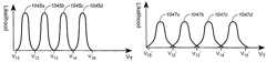
- FIG. 8shows two likelihood functions 839 a - 839 b for the same cell, function 839 a showing the beginning of life distribution of likelihood as a function of threshold voltage V T , and function 839 b showing the end of life distribution of likelihood as a function of threshold voltage V T .
- the beginning of life distribution 839 ais narrower than the end of life distribution 839 b .
- real data from memory cellsshows similar distributions to those of FIG. 8 with the y-axis indicating the number of cells read at different threshold voltages. Likelihood is used for the y-axis in the present description.
- FIGS. 9A and 9BOne way to deal with the widening of likelihood distributions associated with programmed memory states as a memory is used is shown in FIGS. 9A and 9B .
- FIG. 9Ashows four likelihood distributions 941 a - d associated with four programmed states early in the memory's life. Discrimination voltages V 7 , V 8 and V 9 are located between distributions 941 a - d.
- FIG. 9Ashows no significant overlap between adjacent distributions 941 a - d indicating that a large margin is used in this case and the chances of misreading a cell are low.
- FIG. 9Bshows likelihood distributions 943 a - d associated with the same four programmed states of the same cell at a later stage in the memory's life after the cell has undergone a number of memory operations such as reading, programming and erasing.
- the distributions 943 a - dhave widened in comparison with distributions 941 a - d and show some overlap so that there may be a significant likelihood of misreading the stored data.
- Discrimination voltages V 7 -V 9are used to discriminate between memory states as before. Thus, memory states remain mapped to the same threshold window (V 10 -V 11 ), and individual memory states remain mapped to the same sub-ranges within threshold window V 10 -V 11 .
- discrimination voltages V 7 -V 9are initially set at levels that provide a larger margin than needed. This uses a threshold window V 10 to V 11 throughout the memory's life. However, using this wide threshold window may unnecessarily stress the memory because high voltages are needed to program memory cells to high threshold windows such as between V 9 and V 11 .
- FIGS. 10A and 10Bshow an alternative arrangement that uses a smaller threshold window V 15 -V 16 initially and a larger threshold window V 15 ′-V 16 ′ later in the life of the memory.
- memory cell statesare mapped to a narrower threshold window (total threshold voltage range) V 15 -V 16 and subsequently they are mapped to a wider threshold window (total threshold voltage range) V 15 ′-V 16 ′.
- FIG. 10Ashows likelihood functions 1045 a - d for four memory states that are closer together than similar memory states 941 a - d of FIG. 9A . This is the result of programming to target voltages that are arranged to be closer together.
- a programming target voltageis the memory cell threshold voltage that a memory cell is verified as achieving during a programming operation (typically, once a memory cell is verified as reaching the target voltage, further programming of the cell is inhibited, while other cells are programmed further).
- Programming target voltages(in particular the highest programming target voltage) are lower than in FIG. 9A , so programming voltages (e.g. Vprog and Vpass supplied to selected and unselected word lines respectively in NAND memory) may be reduced.
- Discrimination voltages V 12 -V 14define narrower threshold voltage sub-ranges for each memory state during reading. Thus, the threshold window V 15 -V 16 to which memory states are mapped is narrower in this example than threshold window V 10 -V 11 .
- FIG. 10Bshows adjusted discrimination voltages V 12 ′-V 14 ′ that are more widely spaced than discrimination voltages V 12 -V 14 .
- Memory statesare mapped to a wider threshold window (V 15 ′-V 16 ′) in FIG. 10B than the threshold window (V 15 -V 16 ) to which the same memory states were mapped earlier.
- 10A and 10Bcompensates for widening likelihood distributions for individual memory states by increasing the total threshold voltage range to which memory states are mapped.
- One advantage of this schemeis that early in the memory's life, lower voltages are used for programming and reading and these lower voltages provide less stress for the memory cells being read and programmed. Such reduced stress may slow wear-out of memory cells and increase product life.
- Remapping memory states to threshold windowsmay include adjusting programming target voltages as well as read voltages. Programming target voltages are more widely spaced as the memory system goes through its life.
- FIGS. 10A and 10Bshow discrimination voltages V 12 -V 14 and V 12 ′-V 14 ′ used during read operations, though other read voltages may also be used to give a high resolution read that resolves within threshold voltage sub-ranges associated with memory states as described above.
- Generally programming target voltages and read voltagesmay all be adjusted together according to a predetermined scheme or may be individually adjusted in responsive manner, for example in response to information from an ECC decoder. Adjustment may occur in small increments throughout the memory's life or may occur only a limited number of times during the memory life.
- read voltages and programming target voltagesare increased by predetermined amounts in response to a determination that data quality is at a threshold level.
- the threshold levelmay depend on the number of corrections needed, the number of iterations by an iterative decoder, or probability values for memory states when a high resolution read is performed.
- adjustmentmay be made in response to a threshold number of erase operations being performed.
- the programming and reading voltages for the blockmay change when a certain erase count is reached.
- different blocksuse different programming and reading voltages and the memory system keeps track of which block has adjusted voltages using overhead bits within the block, or a table maintained by the controller, or in some other suitable manner using a dedicated circuit, a portion of the controller or other suitable structure.
- Such a systemdoes not necessarily have an ECC decoder that determines quality of data.
- Read voltages and programming target voltagesmay be changed together over the life of a memory. However, some changes to read voltages may be made without changing target voltages. For example, changes may be made to discrimination voltages to balance error corrections between adjacent states where the overall rate of correction is acceptable.
- a read voltagewhen a read voltage is adjusted it remains at the adjusted voltage until a subsequent adjustment is made. However, in some cases it may be desirable to make a temporary adjustment in read voltage. For example, where data is read from a memory and is found to be of poor quality (e.g. low probability values or a high number of errors indicated by ECC), one or more read voltages may be adjusted in a manner determined by ECC correction of the poor quality data, and the data may be read again. This may allow better quality data to be obtained so that the data can be decoded. However, it may not be necessary to keep such read voltages at their adjusted levels. This scheme may be used for retrieving otherwise irretrievable data from a memory.
- ECCerror code
- Such datais then rewritten to another location so that it does not degrade further.
- the original blockmay then be erased. This may be part of a scrub operation carried out by a memory controller or may occur as part of a regular read operation (e.g. in response to a host read command). Programming target voltages generally remain unchanged during an adjustment of this kind. Examples of error handling are given in U.S. Pat. Nos. 5,657,332 and 6,751,766.
- FIG. 11shows a memory system 1149 according to an embodiment of the present invention that includes an ECC module 1151 that has an ECC encoder 1153 , an ECC decoder 1155 and a statistical unit 1157 .
- the statistical unit 1157collects statistical information regarding the corrections carried out by the ECC decoder 1155 .
- the ECC decoder 1155may include a SISO decoder or a hard-input hard-output decoder, or may include both.
- a SISO decoderis concatenated with a hard-input hard-output decoder (the statistical unit may gather statistics regarding decoding by both decoders).
- Two encoding schemesmay be used, such as an LDPC code for SISO decoding and a BCH code for hard-input hard-output decoding.
- the statistical unitmay gather statistics that indicate overall quality of the data and may also indicate numbers of corrections being carried out by the ECC decoding system, or may indicate ratios of corrections between different memory states.
- An output of the statistical unitis provided to an adjustment unit 1159 in a modulation/demodulation circuit 1161 .
- the adjustment unit 1159makes appropriate changes to operating parameters used by a modulator 1163 in programming data to a memory array 1167 (e.g. target voltages for particular memory states) and operating parameters used by a demodulator 1165 in reading data from the memory array 1167 (e.g. read voltages).
- nonvolatile memoriesare currently in use and the techniques described here may be applied to any suitable nonvolatile memory systems.
- memory systemsmay include, but are not limited to, memory systems based on ferroelectric storage (FRAM or FeRAM), memory systems based on magnetoresistive storage (MRAM), and memories based on phase change (PRAM or “OUM” for “Ovonic Unified Memory”).
Landscapes
- Engineering & Computer Science (AREA)
- Theoretical Computer Science (AREA)
- Quality & Reliability (AREA)
- Physics & Mathematics (AREA)
- General Engineering & Computer Science (AREA)
- General Physics & Mathematics (AREA)
- Computer Hardware Design (AREA)
- Read Only Memory (AREA)
- Techniques For Improving Reliability Of Storages (AREA)
Abstract
Description
Claims (13)
Priority Applications (7)
| Application Number | Priority Date | Filing Date | Title |
|---|---|---|---|
| US11/556,626US7558109B2 (en) | 2006-11-03 | 2006-11-03 | Nonvolatile memory with variable read threshold |
| JP2009535412AJP5409371B2 (en) | 2006-11-03 | 2007-10-29 | Nonvolatile memory with variable read threshold |
| EP07863614.9AEP2084709B1 (en) | 2006-11-03 | 2007-10-29 | Nonvolatile memory with variable read threshold |
| PCT/US2007/082831WO2008057822A2 (en) | 2006-11-03 | 2007-10-29 | Nonvolatile memory with variable read threshold |
| KR1020097010854AKR101017847B1 (en) | 2006-11-03 | 2007-10-29 | Nonvolatile Memory with Adjustable Read Threshold |
| CN200780041032.4ACN101573761B (en) | 2006-11-03 | 2007-10-29 | Nonvolatile memory with variable read threshold |
| TW096141224ATWI390533B (en) | 2006-11-03 | 2007-11-01 | Method of managing a flash memory array, method of reading data from a flash memory array, and flash memory system |
Applications Claiming Priority (1)
| Application Number | Priority Date | Filing Date | Title |
|---|---|---|---|
| US11/556,626US7558109B2 (en) | 2006-11-03 | 2006-11-03 | Nonvolatile memory with variable read threshold |
Publications (2)
| Publication Number | Publication Date |
|---|---|
| US20080123420A1 US20080123420A1 (en) | 2008-05-29 |
| US7558109B2true US7558109B2 (en) | 2009-07-07 |
Family
ID=39463514
Family Applications (1)
| Application Number | Title | Priority Date | Filing Date |
|---|---|---|---|
| US11/556,626Active2027-01-17US7558109B2 (en) | 2006-11-03 | 2006-11-03 | Nonvolatile memory with variable read threshold |
Country Status (1)
| Country | Link |
|---|---|
| US (1) | US7558109B2 (en) |
Cited By (177)
| Publication number | Priority date | Publication date | Assignee | Title |
|---|---|---|---|---|
| US20080151621A1 (en)* | 2006-12-26 | 2008-06-26 | Samsung Electronics Co., Ltd. | Multi-level cell memory devices and methods of storing data in and reading data from the memory devices |
| US20080244360A1 (en)* | 2007-03-31 | 2008-10-02 | Nima Mokhlesi | Non-Volatile Memory with Soft Bit Data Transmission for Error Correction Control |
| US20080244338A1 (en)* | 2007-03-31 | 2008-10-02 | Nima Mokhlesi | Soft bit data transmission for error correction control in non-volatile memory |
| US20080244368A1 (en)* | 2007-03-31 | 2008-10-02 | Henry Chin | Guided Simulated Annealing in Non-Volatile Memory Error Correction Control |
| US20080244367A1 (en)* | 2007-03-31 | 2008-10-02 | Henry Chin | Non-volatile memory with guided simulated annealing error correction control |
| US20080250300A1 (en)* | 2007-03-29 | 2008-10-09 | Nima Mokhlesi | Method for decoding data in non-volatile storage using reliability metrics based on multiple reads |
| US20090144600A1 (en)* | 2007-11-30 | 2009-06-04 | Anobit Technologies Ltd | Efficient re-read operations from memory devices |
| US20090207659A1 (en)* | 2008-02-19 | 2009-08-20 | Samsung Electronics Co., Ltd. | Memory device and memory data read method |
| US20100082885A1 (en)* | 2008-09-28 | 2010-04-01 | Ramot At Tel Aviv University Ltd. | Method and system for adaptive coding in flash memories |
| US20100262795A1 (en)* | 2009-04-08 | 2010-10-14 | Steven Robert Hetzler | System, method, and computer program product for analyzing monitor data information from a plurality of memory devices having finite endurance and/or retention |
| US20110216590A1 (en)* | 2010-03-08 | 2011-09-08 | Eun Hee Seok | Nonvolatile memory device using interleaving technology and programmming method thereof |
| US8145984B2 (en) | 2006-10-30 | 2012-03-27 | Anobit Technologies Ltd. | Reading memory cells using multiple thresholds |
| US8151166B2 (en) | 2007-01-24 | 2012-04-03 | Anobit Technologies Ltd. | Reduction of back pattern dependency effects in memory devices |
| US8151163B2 (en) | 2006-12-03 | 2012-04-03 | Anobit Technologies Ltd. | Automatic defect management in memory devices |
| US8156403B2 (en) | 2006-05-12 | 2012-04-10 | Anobit Technologies Ltd. | Combined distortion estimation and error correction coding for memory devices |
| US8156398B2 (en) | 2008-02-05 | 2012-04-10 | Anobit Technologies Ltd. | Parameter estimation based on error correction code parity check equations |
| US8169825B1 (en) | 2008-09-02 | 2012-05-01 | Anobit Technologies Ltd. | Reliable data storage in analog memory cells subjected to long retention periods |
| US8174857B1 (en) | 2008-12-31 | 2012-05-08 | Anobit Technologies Ltd. | Efficient readout schemes for analog memory cell devices using multiple read threshold sets |
| US8174905B2 (en) | 2007-09-19 | 2012-05-08 | Anobit Technologies Ltd. | Programming orders for reducing distortion in arrays of multi-level analog memory cells |
| US8208304B2 (en) | 2008-11-16 | 2012-06-26 | Anobit Technologies Ltd. | Storage at M bits/cell density in N bits/cell analog memory cell devices, M>N |
| US8209588B2 (en) | 2007-12-12 | 2012-06-26 | Anobit Technologies Ltd. | Efficient interference cancellation in analog memory cell arrays |
| US8228701B2 (en) | 2009-03-01 | 2012-07-24 | Apple Inc. | Selective activation of programming schemes in analog memory cell arrays |
| US8230300B2 (en) | 2008-03-07 | 2012-07-24 | Apple Inc. | Efficient readout from analog memory cells using data compression |
| US8234545B2 (en) | 2007-05-12 | 2012-07-31 | Apple Inc. | Data storage with incremental redundancy |
| US8239734B1 (en) | 2008-10-15 | 2012-08-07 | Apple Inc. | Efficient data storage in storage device arrays |
| US8239735B2 (en) | 2006-05-12 | 2012-08-07 | Apple Inc. | Memory Device with adaptive capacity |
| US8238157B1 (en) | 2009-04-12 | 2012-08-07 | Apple Inc. | Selective re-programming of analog memory cells |
| US8243511B2 (en) | 2010-09-27 | 2012-08-14 | Seagate Technology Llc | Reuse of information from memory read operations |
| US8248831B2 (en) | 2008-12-31 | 2012-08-21 | Apple Inc. | Rejuvenation of analog memory cells |
| US8259506B1 (en) | 2009-03-25 | 2012-09-04 | Apple Inc. | Database of memory read thresholds |
| US8259497B2 (en) | 2007-08-06 | 2012-09-04 | Apple Inc. | Programming schemes for multi-level analog memory cells |
| US8261159B1 (en) | 2008-10-30 | 2012-09-04 | Apple, Inc. | Data scrambling schemes for memory devices |
| US8270246B2 (en) | 2007-11-13 | 2012-09-18 | Apple Inc. | Optimized selection of memory chips in multi-chips memory devices |
| US20120236651A1 (en)* | 2010-07-06 | 2012-09-20 | Stec, Inc. | System and method for determining data dependent noise calculation for a flash channel |
| US8276051B2 (en) | 2007-12-12 | 2012-09-25 | Densbits Technologies Ltd. | Chien-search system employing a clock-gating scheme to save power for error correction decoder and other applications |
| US8305812B2 (en) | 2009-08-26 | 2012-11-06 | Densbits Technologies Ltd. | Flash memory module and method for programming a page of flash memory cells |
| US8321625B2 (en) | 2007-12-05 | 2012-11-27 | Densbits Technologies Ltd. | Flash memory device with physical cell value deterioration accommodation and methods useful in conjunction therewith |
| US8327246B2 (en) | 2007-12-18 | 2012-12-04 | Densbits Technologies Ltd. | Apparatus for coding at a plurality of rates in multi-level flash memory systems, and methods useful in conjunction therewith |
| US8332725B2 (en) | 2008-08-20 | 2012-12-11 | Densbits Technologies Ltd. | Reprogramming non volatile memory portions |
| US8335977B2 (en) | 2007-12-05 | 2012-12-18 | Densbits Technologies Ltd. | Flash memory apparatus and methods using a plurality of decoding stages including optional use of concatenated BCH codes and/or designation of “first below” cells |
| US8341502B2 (en) | 2010-02-28 | 2012-12-25 | Densbits Technologies Ltd. | System and method for multi-dimensional decoding |
| US8359516B2 (en) | 2007-12-12 | 2013-01-22 | Densbits Technologies Ltd. | Systems and methods for error correction and decoding on multi-level physical media |
| US8365040B2 (en) | 2007-09-20 | 2013-01-29 | Densbits Technologies Ltd. | Systems and methods for handling immediate data errors in flash memory |
| US8369141B2 (en) | 2007-03-12 | 2013-02-05 | Apple Inc. | Adaptive estimation of memory cell read thresholds |
| US20130033939A1 (en)* | 2011-08-03 | 2013-02-07 | Micron Technology, Inc. | Functional data programming and reading in a memory |
| US8400858B2 (en) | 2008-03-18 | 2013-03-19 | Apple Inc. | Memory device with reduced sense time readout |
| US8429493B2 (en) | 2007-05-12 | 2013-04-23 | Apple Inc. | Memory device with internal signap processing unit |
| US8443242B2 (en) | 2007-10-25 | 2013-05-14 | Densbits Technologies Ltd. | Systems and methods for multiple coding rates in flash devices |
| US8458574B2 (en) | 2009-04-06 | 2013-06-04 | Densbits Technologies Ltd. | Compact chien-search based decoding apparatus and method |
| US8468431B2 (en) | 2010-07-01 | 2013-06-18 | Densbits Technologies Ltd. | System and method for multi-dimensional encoding and decoding |
| US8467249B2 (en) | 2010-07-06 | 2013-06-18 | Densbits Technologies Ltd. | Systems and methods for storing, retrieving, and adjusting read thresholds in flash memory storage system |
| US8479080B1 (en) | 2009-07-12 | 2013-07-02 | Apple Inc. | Adaptive over-provisioning in memory systems |
| US8482978B1 (en) | 2008-09-14 | 2013-07-09 | Apple Inc. | Estimation of memory cell read thresholds by sampling inside programming level distribution intervals |
| US8493783B2 (en) | 2008-03-18 | 2013-07-23 | Apple Inc. | Memory device readout using multiple sense times |
| US8493781B1 (en) | 2010-08-12 | 2013-07-23 | Apple Inc. | Interference mitigation using individual word line erasure operations |
| US8495465B1 (en) | 2009-10-15 | 2013-07-23 | Apple Inc. | Error correction coding over multiple memory pages |
| US8498151B1 (en) | 2008-08-05 | 2013-07-30 | Apple Inc. | Data storage in analog memory cells using modified pass voltages |
| US20130201763A1 (en)* | 2010-12-07 | 2013-08-08 | Silicon Motion Inc. | Method and apparatus for reading data stored in flash memory by referring to binary digit distribution characteristics of bit sequences read from flash memory |
| US8508995B2 (en) | 2010-09-15 | 2013-08-13 | Densbits Technologies Ltd. | System and method for adjusting read voltage thresholds in memories |
| US8516274B2 (en) | 2010-04-06 | 2013-08-20 | Densbits Technologies Ltd. | Method, system and medium for analog encryption in a flash memory |
| US8527819B2 (en) | 2007-10-19 | 2013-09-03 | Apple Inc. | Data storage in analog memory cell arrays having erase failures |
| US8527840B2 (en) | 2010-04-06 | 2013-09-03 | Densbits Technologies Ltd. | System and method for restoring damaged data programmed on a flash device |
| US8539311B2 (en) | 2010-07-01 | 2013-09-17 | Densbits Technologies Ltd. | System and method for data recovery in multi-level cell memories |
| US8553468B2 (en) | 2011-09-21 | 2013-10-08 | Densbits Technologies Ltd. | System and method for managing erase operations in a non-volatile memory |
| US8566510B2 (en) | 2009-05-12 | 2013-10-22 | Densbits Technologies Ltd. | Systems and method for flash memory management |
| US8572423B1 (en) | 2010-06-22 | 2013-10-29 | Apple Inc. | Reducing peak current in memory systems |
| US8572311B1 (en) | 2010-01-11 | 2013-10-29 | Apple Inc. | Redundant data storage in multi-die memory systems |
| US8570804B2 (en) | 2006-05-12 | 2013-10-29 | Apple Inc. | Distortion estimation and cancellation in memory devices |
| US8588003B1 (en) | 2011-08-01 | 2013-11-19 | Densbits Technologies Ltd. | System, method and computer program product for programming and for recovering from a power failure |
| US8595591B1 (en) | 2010-07-11 | 2013-11-26 | Apple Inc. | Interference-aware assignment of programming levels in analog memory cells |
| US8607124B2 (en) | 2009-12-24 | 2013-12-10 | Densbits Technologies Ltd. | System and method for setting a flash memory cell read threshold |
| US8607128B2 (en) | 2007-12-05 | 2013-12-10 | Densbits Technologies Ltd. | Low power chien-search based BCH/RS decoding system for flash memory, mobile communications devices and other applications |
| US8626988B2 (en) | 2009-11-19 | 2014-01-07 | Densbits Technologies Ltd. | System and method for uncoded bit error rate equalization via interleaving |
| US8627175B2 (en) | 2010-09-27 | 2014-01-07 | Seagate Technology Llc | Opportunistic decoding in memory systems |
| US8631288B2 (en) | 2011-03-14 | 2014-01-14 | Micron Technology, Inc. | Methods, devices, and systems for data sensing in a memory system |
| US8645794B1 (en) | 2010-07-31 | 2014-02-04 | Apple Inc. | Data storage in analog memory cells using a non-integer number of bits per cell |
| US8650352B2 (en) | 2007-09-20 | 2014-02-11 | Densbits Technologies Ltd. | Systems and methods for determining logical values of coupled flash memory cells |
| US8667211B2 (en) | 2011-06-01 | 2014-03-04 | Densbits Technologies Ltd. | System and method for managing a non-volatile memory |
| US8671327B2 (en) | 2008-09-28 | 2014-03-11 | Sandisk Technologies Inc. | Method and system for adaptive coding in flash memories |
| US8677054B1 (en) | 2009-12-16 | 2014-03-18 | Apple Inc. | Memory management schemes for non-volatile memory devices |
| US8694853B1 (en) | 2010-05-04 | 2014-04-08 | Apple Inc. | Read commands for reading interfering memory cells |
| US8694854B1 (en) | 2010-08-17 | 2014-04-08 | Apple Inc. | Read threshold setting based on soft readout statistics |
| US8693257B2 (en) | 2011-10-18 | 2014-04-08 | Seagate Technology Llc | Determining optimal read reference and programming voltages for non-volatile memory using mutual information |
| US8693258B2 (en) | 2011-03-17 | 2014-04-08 | Densbits Technologies Ltd. | Obtaining soft information using a hard interface |
| US8694814B1 (en) | 2010-01-10 | 2014-04-08 | Apple Inc. | Reuse of host hibernation storage space by memory controller |
| US8694715B2 (en) | 2007-10-22 | 2014-04-08 | Densbits Technologies Ltd. | Methods for adaptively programming flash memory devices and flash memory systems incorporating same |
| US8711619B2 (en) | 2011-10-18 | 2014-04-29 | Seagate Technology Llc | Categorizing bit errors of solid-state, non-volatile memory |
| US8724387B2 (en) | 2009-10-22 | 2014-05-13 | Densbits Technologies Ltd. | Method, system, and computer readable medium for reading and programming flash memory cells using multiple bias voltages |
| US8730729B2 (en) | 2009-10-15 | 2014-05-20 | Densbits Technologies Ltd. | Systems and methods for averaging error rates in non-volatile devices and storage systems |
| US8737133B2 (en) | 2011-10-18 | 2014-05-27 | Seagate Technology Llc | Shifting cell voltage based on grouping of solid-state, non-volatile memory cells |
| US8745317B2 (en) | 2010-04-07 | 2014-06-03 | Densbits Technologies Ltd. | System and method for storing information in a multi-level cell memory |
| US8760932B2 (en) | 2011-10-18 | 2014-06-24 | Seagate Technology Llc | Determination of memory read reference and programming voltages |
| US8819385B2 (en) | 2009-04-06 | 2014-08-26 | Densbits Technologies Ltd. | Device and method for managing a flash memory |
| US8832354B2 (en) | 2009-03-25 | 2014-09-09 | Apple Inc. | Use of host system resources by memory controller |
| US8838937B1 (en) | 2012-05-23 | 2014-09-16 | Densbits Technologies Ltd. | Methods, systems and computer readable medium for writing and reading data |
| US8850100B2 (en) | 2010-12-07 | 2014-09-30 | Densbits Technologies Ltd. | Interleaving codeword portions between multiple planes and/or dies of a flash memory device |
| US8856475B1 (en) | 2010-08-01 | 2014-10-07 | Apple Inc. | Efficient selection of memory blocks for compaction |
| US8868821B2 (en) | 2009-08-26 | 2014-10-21 | Densbits Technologies Ltd. | Systems and methods for pre-equalization and code design for a flash memory |
| US8879325B1 (en) | 2012-05-30 | 2014-11-04 | Densbits Technologies Ltd. | System, method and computer program product for processing read threshold information and for reading a flash memory module |
| US8908460B2 (en) | 2011-05-17 | 2014-12-09 | Samsung Electronics Co., Ltd. | Nonvolatile memory systems using time-dependent read voltages and methods of operating the same |
| US8924661B1 (en) | 2009-01-18 | 2014-12-30 | Apple Inc. | Memory system including a controller and processors associated with memory devices |
| US8924824B1 (en) | 2013-03-12 | 2014-12-30 | Western Digital Technologies, Inc. | Soft-decision input generation for data storage systems |
| US8942037B2 (en) | 2012-10-31 | 2015-01-27 | Lsi Corporation | Threshold acquisition and adaption in NAND flash memory |
| US8947941B2 (en) | 2012-02-09 | 2015-02-03 | Densbits Technologies Ltd. | State responsive operations relating to flash memory cells |
| US8949684B1 (en) | 2008-09-02 | 2015-02-03 | Apple Inc. | Segmented data storage |
| US8964464B2 (en) | 2010-08-24 | 2015-02-24 | Densbits Technologies Ltd. | System and method for accelerated sampling |
| US8972472B2 (en) | 2008-03-25 | 2015-03-03 | Densbits Technologies Ltd. | Apparatus and methods for hardware-efficient unbiased rounding |
| US8990665B1 (en) | 2011-04-06 | 2015-03-24 | Densbits Technologies Ltd. | System, method and computer program product for joint search of a read threshold and soft decoding |
| US20150089330A1 (en)* | 2013-09-26 | 2015-03-26 | Lsi Corporation | Systems and Methods for Enhanced Data Recovery in a Solid State Memory System |
| US8996790B1 (en) | 2011-05-12 | 2015-03-31 | Densbits Technologies Ltd. | System and method for flash memory management |
| US8996788B2 (en) | 2012-02-09 | 2015-03-31 | Densbits Technologies Ltd. | Configurable flash interface |
| US8995197B1 (en) | 2009-08-26 | 2015-03-31 | Densbits Technologies Ltd. | System and methods for dynamic erase and program control for flash memory device memories |
| US8996793B1 (en) | 2012-04-24 | 2015-03-31 | Densbits Technologies Ltd. | System, method and computer readable medium for generating soft information |
| US9007854B1 (en) | 2013-12-09 | 2015-04-14 | Western Digital Technologies, Inc. | Method and system for optimized soft decoding in a data storage device |
| US9021177B2 (en) | 2010-04-29 | 2015-04-28 | Densbits Technologies Ltd. | System and method for allocating and using spare blocks in a flash memory |
| US9021181B1 (en) | 2010-09-27 | 2015-04-28 | Apple Inc. | Memory management for unifying memory cell conditions by using maximum time intervals |
| US9037777B2 (en) | 2009-12-22 | 2015-05-19 | Densbits Technologies Ltd. | Device, system, and method for reducing program/read disturb in flash arrays |
| US9036420B2 (en) | 2009-03-27 | 2015-05-19 | Analog Devices, Inc. | Storage devices with soft processing |
| US20150138888A1 (en)* | 2009-11-06 | 2015-05-21 | Kabushiki Kaisha Toshiba | Memory system |
| US20150149701A1 (en)* | 2013-11-22 | 2015-05-28 | Phison Electronics Corp. | Time estimating method, memory storage device, and memory controlling circuit unit |
| US9063878B2 (en) | 2010-11-03 | 2015-06-23 | Densbits Technologies Ltd. | Method, system and computer readable medium for copy back |
| US9069659B1 (en) | 2013-01-03 | 2015-06-30 | Densbits Technologies Ltd. | Read threshold determination using reference read threshold |
| US9104580B1 (en) | 2010-07-27 | 2015-08-11 | Apple Inc. | Cache memory for hybrid disk drives |
| US9110785B1 (en) | 2011-05-12 | 2015-08-18 | Densbits Technologies Ltd. | Ordered merge of data sectors that belong to memory space portions |
| US9136876B1 (en) | 2013-06-13 | 2015-09-15 | Densbits Technologies Ltd. | Size limited multi-dimensional decoding |
| US9135109B2 (en) | 2013-03-11 | 2015-09-15 | Seagate Technology Llc | Determination of optimum threshold voltage to read data values in memory cells |
| US9195592B1 (en) | 2011-05-12 | 2015-11-24 | Densbits Technologies Ltd. | Advanced management of a non-volatile memory |
| US9270296B1 (en) | 2013-11-13 | 2016-02-23 | Western Digital Technologies, Inc. | Method and system for soft decoding through single read |
| US9330767B1 (en) | 2009-08-26 | 2016-05-03 | Avago Technologies General Ip (Singapore) Pte. Ltd. | Flash memory module and method for programming a page of flash memory cells |
| US9348694B1 (en) | 2013-10-09 | 2016-05-24 | Avago Technologies General Ip (Singapore) Pte. Ltd. | Detecting and managing bad columns |
| US9361222B2 (en) | 2013-08-07 | 2016-06-07 | SMART Storage Systems, Inc. | Electronic system with storage drive life estimation mechanism and method of operation thereof |
| US9368225B1 (en) | 2012-11-21 | 2016-06-14 | Avago Technologies General Ip (Singapore) Pte. Ltd. | Determining read thresholds based upon read error direction statistics |
| US9372792B1 (en) | 2011-05-12 | 2016-06-21 | Avago Technologies General Ip (Singapore) Pte. Ltd. | Advanced management of a non-volatile memory |
| US9397706B1 (en) | 2013-10-09 | 2016-07-19 | Avago Technologies General Ip (Singapore) Pte. Ltd. | System and method for irregular multiple dimension decoding and encoding |
| US9396106B2 (en) | 2011-05-12 | 2016-07-19 | Avago Technologies General Ip (Singapore) Pte. Ltd. | Advanced management of a non-volatile memory |
| US9407291B1 (en) | 2014-07-03 | 2016-08-02 | Avago Technologies General Ip (Singapore) Pte. Ltd. | Parallel encoding method and system |
| US9413491B1 (en) | 2013-10-08 | 2016-08-09 | Avago Technologies General Ip (Singapore) Pte. Ltd. | System and method for multiple dimension decoding and encoding a message |
| US9431113B2 (en) | 2013-08-07 | 2016-08-30 | Sandisk Technologies Llc | Data storage system with dynamic erase block grouping mechanism and method of operation thereof |
| US9449702B1 (en) | 2014-07-08 | 2016-09-20 | Avago Technologies General Ip (Singapore) Pte. Ltd. | Power management |
| US9448946B2 (en) | 2013-08-07 | 2016-09-20 | Sandisk Technologies Llc | Data storage system with stale data mechanism and method of operation thereof |
| US9501392B1 (en) | 2011-05-12 | 2016-11-22 | Avago Technologies General Ip (Singapore) Pte. Ltd. | Management of a non-volatile memory module |
| US9502117B2 (en) | 2011-03-14 | 2016-11-22 | Seagate Technology Llc | Cell-level statistics collection for detection and decoding in flash memories |
| US9524211B1 (en) | 2014-11-18 | 2016-12-20 | Avago Technologies General Ip (Singapore) Pte. Ltd. | Codeword management |
| US9536612B1 (en) | 2014-01-23 | 2017-01-03 | Avago Technologies General Ip (Singapore) Pte. Ltd | Digital signaling processing for three dimensional flash memory arrays |
| US9543025B2 (en) | 2013-04-11 | 2017-01-10 | Sandisk Technologies Llc | Storage control system with power-off time estimation mechanism and method of operation thereof |
| US9542262B1 (en) | 2014-05-29 | 2017-01-10 | Avago Technologies General Ip (Singapore) Pte. Ltd. | Error correction |
| US9542258B1 (en) | 2013-03-15 | 2017-01-10 | Western Digital Technologies, Inc. | System and method for error-minimizing voltage threshold selection |
| TWI579854B (en)* | 2010-03-12 | 2017-04-21 | Lsi公司 | Ldpc erasure decoding for flash memories |
| US9747157B2 (en) | 2013-11-08 | 2017-08-29 | Sandisk Technologies Llc | Method and system for improving error correction in data storage |
| US9786388B1 (en) | 2013-10-09 | 2017-10-10 | Avago Technologies General Ip (Singapore) Pte. Ltd. | Detecting and managing bad columns |
| US9851921B1 (en) | 2015-07-05 | 2017-12-26 | Avago Technologies General Ip (Singapore) Pte. Ltd. | Flash memory chip processing |
| US9875804B2 (en) | 2016-03-02 | 2018-01-23 | Toshiba Memory Corporation | Nonvolatile semiconductor memory device with read voltage setting controller |
| US9892033B1 (en) | 2014-06-24 | 2018-02-13 | Avago Technologies General Ip (Singapore) Pte. Ltd. | Management of memory units |
| US9898361B2 (en) | 2011-01-04 | 2018-02-20 | Seagate Technology Llc | Multi-tier detection and decoding in flash memories |
| US9921954B1 (en) | 2012-08-27 | 2018-03-20 | Avago Technologies General Ip (Singapore) Pte. Ltd. | Method and system for split flash memory management between host and storage controller |
| US9954558B1 (en) | 2016-03-03 | 2018-04-24 | Avago Technologies General Ip (Singapore) Pte. Ltd. | Fast decoding of data stored in a flash memory |
| US9972393B1 (en) | 2014-07-03 | 2018-05-15 | Avago Technologies General Ip (Singapore) Pte. Ltd. | Accelerating programming of a flash memory module |
| US9971646B2 (en) | 2016-06-01 | 2018-05-15 | Apple Inc. | Reading-threshold setting based on data encoded with a multi-component code |
| US10049037B2 (en) | 2013-04-05 | 2018-08-14 | Sandisk Enterprise Ip Llc | Data management in a storage system |
| US10061640B1 (en) | 2013-03-12 | 2018-08-28 | Western Digital Technologies, Inc. | Soft-decision input generation for data storage systems |
| US10079068B2 (en) | 2011-02-23 | 2018-09-18 | Avago Technologies General Ip (Singapore) Pte. Ltd. | Devices and method for wear estimation based memory management |
| US10120792B1 (en) | 2014-01-29 | 2018-11-06 | Avago Technologies General Ip (Singapore) Pte. Ltd. | Programming an embedded flash storage device |
| US10163523B2 (en)* | 2015-03-31 | 2018-12-25 | SK Hynix Inc. | Semiconductor device and operating method thereof |
| US10304550B1 (en) | 2017-11-29 | 2019-05-28 | Sandisk Technologies Llc | Sense amplifier with negative threshold sensing for non-volatile memory |
| US10305515B1 (en) | 2015-02-02 | 2019-05-28 | Avago Technologies International Sales Pte. Limited | System and method for encoding using multiple linear feedback shift registers |
| US10446254B1 (en)* | 2018-05-03 | 2019-10-15 | Western Digital Technologies, Inc. | Method for maximizing power efficiency in memory interface block |
| US10546648B2 (en) | 2013-04-12 | 2020-01-28 | Sandisk Technologies Llc | Storage control system with data management mechanism and method of operation thereof |
| US10628255B1 (en) | 2015-06-11 | 2020-04-21 | Avago Technologies International Sales Pte. Limited | Multi-dimensional decoding |
| US10643695B1 (en) | 2019-01-10 | 2020-05-05 | Sandisk Technologies Llc | Concurrent multi-state program verify for non-volatile memory |
| US20200210831A1 (en)* | 2018-12-31 | 2020-07-02 | SK Hynix Inc. | Storage device performance optimization using deep learning |
| US10719396B2 (en)* | 2018-03-19 | 2020-07-21 | Toshiba Memory Corporation | Memory system |
| US10783973B1 (en) | 2019-11-26 | 2020-09-22 | Winbond Electronics Corp. | Memory device having parameter adjusting mechanism and method of adjusting parameter by memory device |
| US11004525B1 (en) | 2020-02-20 | 2021-05-11 | Sandisk Technologies Llc | Modulation of programming voltage during cycling |
| US11024392B1 (en) | 2019-12-23 | 2021-06-01 | Sandisk Technologies Llc | Sense amplifier for bidirectional sensing of memory cells of a non-volatile memory |
| US11556416B2 (en) | 2021-05-05 | 2023-01-17 | Apple Inc. | Controlling memory readout reliability and throughput by adjusting distance between read thresholds |
| US11847342B2 (en) | 2021-07-28 | 2023-12-19 | Apple Inc. | Efficient transfer of hard data and confidence levels in reading a nonvolatile memory |
| US11960989B2 (en) | 2020-07-24 | 2024-04-16 | SK Hynix Inc. | Read threshold estimation systems and methods using deep learning |
Families Citing this family (68)
| Publication number | Priority date | Publication date | Assignee | Title |
|---|---|---|---|---|
| WO2007132452A2 (en) | 2006-05-12 | 2007-11-22 | Anobit Technologies | Reducing programming error in memory devices |
| WO2008026203A2 (en) | 2006-08-27 | 2008-03-06 | Anobit Technologies | Estimation of non-linear distortion in memory devices |
| US7886204B2 (en)* | 2006-09-27 | 2011-02-08 | Sandisk Corporation | Methods of cell population distribution assisted read margining |
| US20080092015A1 (en)* | 2006-09-28 | 2008-04-17 | Yigal Brandman | Nonvolatile memory with adaptive operation |
| US7805663B2 (en)* | 2006-09-28 | 2010-09-28 | Sandisk Corporation | Methods of adapting operation of nonvolatile memory |
| US7904783B2 (en)* | 2006-09-28 | 2011-03-08 | Sandisk Corporation | Soft-input soft-output decoder for nonvolatile memory |
| US7818653B2 (en) | 2006-09-28 | 2010-10-19 | Sandisk Corporation | Methods of soft-input soft-output decoding for nonvolatile memory |
| WO2008053473A2 (en) | 2006-10-30 | 2008-05-08 | Anobit Technologies Ltd. | Memory cell readout using successive approximation |
| US7904780B2 (en)* | 2006-11-03 | 2011-03-08 | Sandisk Corporation | Methods of modulating error correction coding |
| US8001441B2 (en)* | 2006-11-03 | 2011-08-16 | Sandisk Technologies Inc. | Nonvolatile memory with modulated error correction coding |
| US7904788B2 (en)* | 2006-11-03 | 2011-03-08 | Sandisk Corporation | Methods of varying read threshold voltage in nonvolatile memory |
| US7924648B2 (en) | 2006-11-28 | 2011-04-12 | Anobit Technologies Ltd. | Memory power and performance management |
| US7593263B2 (en) | 2006-12-17 | 2009-09-22 | Anobit Technologies Ltd. | Memory device with reduced reading latency |
| US7900102B2 (en) | 2006-12-17 | 2011-03-01 | Anobit Technologies Ltd. | High-speed programming of memory devices |
| US7751240B2 (en) | 2007-01-24 | 2010-07-06 | Anobit Technologies Ltd. | Memory device with negative thresholds |
| US8001320B2 (en) | 2007-04-22 | 2011-08-16 | Anobit Technologies Ltd. | Command interface for memory devices |
| US7925936B1 (en) | 2007-07-13 | 2011-04-12 | Anobit Technologies Ltd. | Memory device with non-uniform programming levels |
| US7773413B2 (en) | 2007-10-08 | 2010-08-10 | Anobit Technologies Ltd. | Reliable data storage in analog memory cells in the presence of temperature variations |
| US8068360B2 (en) | 2007-10-19 | 2011-11-29 | Anobit Technologies Ltd. | Reading analog memory cells using built-in multi-threshold commands |
| US8000141B1 (en) | 2007-10-19 | 2011-08-16 | Anobit Technologies Ltd. | Compensation for voltage drifts in analog memory cells |
| US8456905B2 (en) | 2007-12-16 | 2013-06-04 | Apple Inc. | Efficient data storage in multi-plane memory devices |
| US8085586B2 (en) | 2007-12-27 | 2011-12-27 | Anobit Technologies Ltd. | Wear level estimation in analog memory cells |
| US7924587B2 (en) | 2008-02-21 | 2011-04-12 | Anobit Technologies Ltd. | Programming of analog memory cells using a single programming pulse per state transition |
| US7864573B2 (en) | 2008-02-24 | 2011-01-04 | Anobit Technologies Ltd. | Programming analog memory cells for reduced variance after retention |
| KR101378365B1 (en)* | 2008-03-12 | 2014-03-28 | 삼성전자주식회사 | Apparatus and method for hybrid detecting memory data |
| US8059457B2 (en) | 2008-03-18 | 2011-11-15 | Anobit Technologies Ltd. | Memory device with multiple-accuracy read commands |
| US7924613B1 (en) | 2008-08-05 | 2011-04-12 | Anobit Technologies Ltd. | Data storage in analog memory cells with protection against programming interruption |
| US8000135B1 (en) | 2008-09-14 | 2011-08-16 | Anobit Technologies Ltd. | Estimation of memory cell read thresholds by sampling inside programming level distribution intervals |
| US8830748B2 (en) | 2008-09-30 | 2014-09-09 | Lsi Corporation | Methods and apparatus for soft data generation for memory devices |
| US8947929B1 (en)* | 2008-11-06 | 2015-02-03 | Marvell International Ltd. | Flash-based soft information generation |
| US8611151B1 (en) | 2008-11-06 | 2013-12-17 | Marvell International Ltd. | Flash memory read performance |
| US7764550B2 (en)* | 2008-11-25 | 2010-07-27 | Freescale Semiconductor, Inc. | Method of programming a non-volatile memory |
| KR20100072717A (en)* | 2008-12-22 | 2010-07-01 | 삼성전자주식회사 | Data processing method and apparatus |
| US8458114B2 (en)* | 2009-03-02 | 2013-06-04 | Analog Devices, Inc. | Analog computation using numerical representations with uncertainty |
| US20100220514A1 (en)* | 2009-03-02 | 2010-09-02 | Lyric Semiconductor, Inc. | Storage devices with soft processing |
| US8213236B1 (en) | 2009-04-21 | 2012-07-03 | Marvell International Ltd. | Flash memory |
| US8775913B2 (en) | 2010-03-31 | 2014-07-08 | Lsi Corporation | Methods and apparatus for computing soft data or log likelihood ratios for received values in communication or storage systems |
| US8504885B2 (en) | 2010-03-31 | 2013-08-06 | Lsi Corporation | Methods and apparatus for approximating a probability density function or distribution for a received value in communication or storage systems |
| US8429500B2 (en) | 2010-03-31 | 2013-04-23 | Lsi Corporation | Methods and apparatus for computing a probability value of a received value in communication or storage systems |
| US8756394B1 (en) | 2010-07-07 | 2014-06-17 | Marvell International Ltd. | Multi-dimension memory timing tuner |
| KR101792868B1 (en)* | 2010-11-25 | 2017-11-02 | 삼성전자주식회사 | Flash memory device and reading method thereof |
| US9292377B2 (en) | 2011-01-04 | 2016-03-22 | Seagate Technology Llc | Detection and decoding in flash memories using correlation of neighboring bits and probability based reliability values |
| US8687421B2 (en)* | 2011-11-21 | 2014-04-01 | Sandisk Technologies Inc. | Scrub techniques for use with dynamic read |
| US8681569B2 (en)* | 2012-02-22 | 2014-03-25 | Silicon Motion, Inc. | Method for reading data stored in a flash memory according to a threshold voltage distribution and memory controller and system thereof |
| CN103325412B (en)* | 2012-03-20 | 2016-08-03 | 旺宏电子股份有限公司 | Integrated circuit with dynamic sensing interval and method of operation thereof |
| US9257203B2 (en)* | 2012-12-06 | 2016-02-09 | Micron Technology, Inc. | Setting a default read signal based on error correction |
| US20140281842A1 (en)* | 2013-03-14 | 2014-09-18 | Fusion-Io, Inc. | Non-Volatile Cells Having a Non-Power-of-Two Number of States |
| US9013920B2 (en)* | 2013-04-03 | 2015-04-21 | Western Digital Technologies, Inc. | Systems and methods of write precompensation to extend life of a solid-state memory |
| CN110232942B (en) | 2013-09-13 | 2023-01-03 | 铠侠股份有限公司 | Storage device and control method thereof |
| CN104616695B (en)* | 2013-11-05 | 2017-12-22 | 光宝科技股份有限公司 | Solid-state memory device and read voltage setting method thereof |
| US20150205664A1 (en)* | 2014-01-17 | 2015-07-23 | Fusion-Io, Inc. | Determining a configuration parameter using a soft read command |
| US9230689B2 (en) | 2014-03-17 | 2016-01-05 | Sandisk Technologies Inc. | Finding read disturbs on non-volatile memories |
| US9552171B2 (en) | 2014-10-29 | 2017-01-24 | Sandisk Technologies Llc | Read scrub with adaptive counter management |
| DE102014115885B4 (en)* | 2014-10-31 | 2018-03-08 | Infineon Technologies Ag | Health state of non-volatile memory |
| US9978456B2 (en) | 2014-11-17 | 2018-05-22 | Sandisk Technologies Llc | Techniques for reducing read disturb in partially written blocks of non-volatile memory |
| US9349479B1 (en) | 2014-11-18 | 2016-05-24 | Sandisk Technologies Inc. | Boundary word line operation in nonvolatile memory |
| US9449700B2 (en) | 2015-02-13 | 2016-09-20 | Sandisk Technologies Llc | Boundary word line search and open block read methods with reduced read disturb |
| US9653154B2 (en) | 2015-09-21 | 2017-05-16 | Sandisk Technologies Llc | Write abort detection for multi-state memories |
| CN108023670A (en)* | 2016-11-04 | 2018-05-11 | 展讯通信(上海)有限公司 | One kind packet code coding method and device |
| KR20180100984A (en)* | 2017-03-03 | 2018-09-12 | 에스케이하이닉스 주식회사 | Memory system and operating method of memory system |
| US10678633B2 (en)* | 2017-11-30 | 2020-06-09 | SK Hynix Inc. | Memory system and operating method thereof |
| US11270771B2 (en)* | 2019-01-29 | 2022-03-08 | Silicon Storage Technology, Inc. | Neural network classifier using array of stacked gate non-volatile memory cells |
| US11119697B2 (en)* | 2019-07-12 | 2021-09-14 | Micron Technology, Inc. | Read voltage management based on write-to-read time difference |
| KR20210156563A (en)* | 2020-06-18 | 2021-12-27 | 삼성전자주식회사 | Error check code (ECC) decoder and a memory system including an ECC decoder |
| TWI768496B (en)* | 2020-10-07 | 2022-06-21 | 群聯電子股份有限公司 | Read voltage control method, memory storage device and memory control circuit unit |
| CN112201285B (en)* | 2020-10-16 | 2024-08-06 | 群联电子股份有限公司 | Voltage control method, memory storage device and memory control circuit unit |
| TWI800764B (en)* | 2020-10-30 | 2023-05-01 | 群聯電子股份有限公司 | Memory control method, memory storage device and memory control circuit unit |
| US11437111B2 (en)* | 2020-12-15 | 2022-09-06 | Micron Technology, Inc. | Trims corresponding to program/erase cycles |
Citations (52)
| Publication number | Priority date | Publication date | Assignee | Title |
|---|---|---|---|---|
| US5043940A (en) | 1988-06-08 | 1991-08-27 | Eliyahou Harari | Flash EEPROM memory systems having multistate storage cells |
| US5070032A (en) | 1989-03-15 | 1991-12-03 | Sundisk Corporation | Method of making dense flash eeprom semiconductor memory structures |
| US5095344A (en) | 1988-06-08 | 1992-03-10 | Eliyahou Harari | Highly compact eprom and flash eeprom devices |
| US5172338A (en) | 1989-04-13 | 1992-12-15 | Sundisk Corporation | Multi-state EEprom read and write circuits and techniques |
| US5313421A (en) | 1992-01-14 | 1994-05-17 | Sundisk Corporation | EEPROM with split gate source side injection |
| US5315541A (en) | 1992-07-24 | 1994-05-24 | Sundisk Corporation | Segmented column memory array |
| US5343063A (en) | 1990-12-18 | 1994-08-30 | Sundisk Corporation | Dense vertical programmable read only memory cell structure and processes for making them |
| US5532962A (en) | 1992-05-20 | 1996-07-02 | Sandisk Corporation | Soft errors handling in EEPROM devices |
| US5570315A (en) | 1993-09-21 | 1996-10-29 | Kabushiki Kaisha Toshiba | Multi-state EEPROM having write-verify control circuit |
| US5657332A (en) | 1992-05-20 | 1997-08-12 | Sandisk Corporation | Soft errors handling in EEPROM devices |
| US5661053A (en) | 1994-05-25 | 1997-08-26 | Sandisk Corporation | Method of making dense flash EEPROM cell array and peripheral supporting circuits formed in deposited field oxide with the use of spacers |
| EP0802540A2 (en) | 1996-04-19 | 1997-10-22 | Kabushiki Kaisha Toshiba | Multilevel memory system |
| US5774397A (en) | 1993-06-29 | 1998-06-30 | Kabushiki Kaisha Toshiba | Non-volatile semiconductor memory device and method of programming a non-volatile memory cell to a predetermined state |
| US5909449A (en) | 1997-09-08 | 1999-06-01 | Invox Technology | Multibit-per-cell non-volatile memory with error detection and correction |
| US5930167A (en) | 1997-07-30 | 1999-07-27 | Sandisk Corporation | Multi-state non-volatile flash memory capable of being its own two state write cache |
| US6046935A (en) | 1996-03-18 | 2000-04-04 | Kabushiki Kaisha Toshiba | Semiconductor device and memory system |
| US6222762B1 (en) | 1992-01-14 | 2001-04-24 | Sandisk Corporation | Multi-state memory |
| US6266276B1 (en)* | 1998-12-17 | 2001-07-24 | Fujitsu Limited | Non-volatile semiconductor memory device and internal operation method for said non-volatile semiconductor memory device |
| US6339546B1 (en) | 1999-09-17 | 2002-01-15 | Hitachi, Ltd. | Storage device counting error correction |
| US6397364B1 (en) | 1998-04-20 | 2002-05-28 | Mordecai Barkan | Digital data representation for multi-bit data storage and transmission |
| US6456528B1 (en) | 2001-09-17 | 2002-09-24 | Sandisk Corporation | Selective operation of a multi-state non-volatile memory system in a binary mode |
| US6467062B1 (en) | 1997-12-10 | 2002-10-15 | Mordecai Barkan | Digital data (multi-bit) storage with discrete analog memory cells |
| US6469931B1 (en) | 2001-01-04 | 2002-10-22 | M-Systems Flash Disk Pioneers Ltd. | Method for increasing information content in a computer memory |
| US6522580B2 (en) | 2001-06-27 | 2003-02-18 | Sandisk Corporation | Operating techniques for reducing effects of coupling between storage elements of a non-volatile memory operated in multiple data states |
| US6674385B2 (en) | 2000-10-31 | 2004-01-06 | Stmicroelectronics S.R.L. | Analog-to-digital conversion method and device, in high-density multilevel non-volatile memory devices |
| US6751766B2 (en) | 2002-05-20 | 2004-06-15 | Sandisk Corporation | Increasing the effectiveness of error correction codes and operating multi-level memory systems by using information about the quality of the stored data |
| US6785164B2 (en) | 2002-01-18 | 2004-08-31 | Sandisk Corporation | Reducing the effects of noise in non-volatile memories through multiple reads |
| US6873549B2 (en) | 2000-09-27 | 2005-03-29 | Sandisk Corporation | Writable tracking cells |
| US6925007B2 (en) | 2001-10-31 | 2005-08-02 | Sandisk Corporation | Multi-state non-volatile integrated circuit memory systems that employ dielectric storage elements |
| US6941412B2 (en) | 2002-08-29 | 2005-09-06 | Sandisk Corporation | Symbol frequency leveling in a storage system |
| US20050204212A1 (en) | 2004-02-27 | 2005-09-15 | Mitsuhiro Noguchi | Data memory system |
| US20050213393A1 (en) | 2004-03-14 | 2005-09-29 | M-Systems Flash Disk Pioneers, Ltd. | States encoding in multi-bit flash cells for optimizing error rate |
| US6977844B2 (en) | 2000-10-31 | 2005-12-20 | Sandisk Corporation | Method of reducing disturbs in non-volatile memory |
| US6983428B2 (en) | 2002-09-24 | 2006-01-03 | Sandisk Corporation | Highly compact non-volatile memory and method thereof |
| US7012835B2 (en)* | 2003-10-03 | 2006-03-14 | Sandisk Corporation | Flash memory data correction and scrub techniques |
| US7035146B2 (en) | 2004-01-21 | 2006-04-25 | Sandisk Corporation | Programming non-volatile memory |
| US20060101193A1 (en) | 2004-11-08 | 2006-05-11 | M-Systems Flash Disk Pioneers, Ltd. | States encoding in multi-bit flash cells for optimizing error rate |
| US7088621B2 (en) | 2004-05-05 | 2006-08-08 | Sandisk Corporation | Bitline governed approach for coarse/fine programming |
| US7092290B2 (en) | 2004-11-16 | 2006-08-15 | Sandisk Corporation | High speed programming system with reduced over programming |
| US20070076487A1 (en)* | 2005-09-30 | 2007-04-05 | Ken Takeuchi | Semiconductor integrated circuit device |
| US20070150791A1 (en) | 2005-12-27 | 2007-06-28 | Gross Stephen J | Storing downloadable firmware on bulk media |
| US20070150790A1 (en) | 2005-12-27 | 2007-06-28 | Gross Stephen J | Method of storing downloadable firmware on bulk media |
| US20070208905A1 (en)* | 2006-03-06 | 2007-09-06 | Ramot At Tel-Aviv University Ltd. | Multi-bit-per-cell flash memory device with non-bijective mapping |
| US20070266295A1 (en) | 2006-05-15 | 2007-11-15 | Conley Kevin M | Convolutional Coding Methods for Nonvolatile Memory |
| US20070266296A1 (en) | 2006-05-15 | 2007-11-15 | Conley Kevin M | Nonvolatile Memory with Convolutional Coding |
| US20080082897A1 (en) | 2006-09-28 | 2008-04-03 | Yigal Brandman | Soft-Input Soft-Output Decoder for Nonvolatile Memory |
| US20080092026A1 (en) | 2006-09-28 | 2008-04-17 | Yigal Brandman | Methods of Soft-Input Soft-Output Decoding for Nonvolatile Memory |
| US20080092015A1 (en) | 2006-09-28 | 2008-04-17 | Yigal Brandman | Nonvolatile memory with adaptive operation |
| US20080092014A1 (en) | 2006-09-28 | 2008-04-17 | Yigal Brandman | Methods of Adapting Operation of Nonvolatile Memory |
| US20080109702A1 (en) | 2006-11-03 | 2008-05-08 | Yigal Brandman | Methods of Modulating Error Correction Coding |
| US20080109703A1 (en) | 2006-11-03 | 2008-05-08 | Yigal Brandman | Nonvolatile Memory With Modulated Error Correction Coding |
| US20080123419A1 (en) | 2006-11-03 | 2008-05-29 | Yigal Brandman | Methods of Varying Read Threshold Voltage in Nonvolatile Memory |
- 2006
- 2006-11-03USUS11/556,626patent/US7558109B2/enactiveActive
Patent Citations (55)
| Publication number | Priority date | Publication date | Assignee | Title |
|---|---|---|---|---|
| US5095344A (en) | 1988-06-08 | 1992-03-10 | Eliyahou Harari | Highly compact eprom and flash eeprom devices |
| US5043940A (en) | 1988-06-08 | 1991-08-27 | Eliyahou Harari | Flash EEPROM memory systems having multistate storage cells |
| US5070032A (en) | 1989-03-15 | 1991-12-03 | Sundisk Corporation | Method of making dense flash eeprom semiconductor memory structures |
| US5172338A (en) | 1989-04-13 | 1992-12-15 | Sundisk Corporation | Multi-state EEprom read and write circuits and techniques |
| US5172338B1 (en) | 1989-04-13 | 1997-07-08 | Sandisk Corp | Multi-state eeprom read and write circuits and techniques |
| US5343063A (en) | 1990-12-18 | 1994-08-30 | Sundisk Corporation | Dense vertical programmable read only memory cell structure and processes for making them |
| US5313421A (en) | 1992-01-14 | 1994-05-17 | Sundisk Corporation | EEPROM with split gate source side injection |
| US6222762B1 (en) | 1992-01-14 | 2001-04-24 | Sandisk Corporation | Multi-state memory |
| US5532962A (en) | 1992-05-20 | 1996-07-02 | Sandisk Corporation | Soft errors handling in EEPROM devices |
| US5657332A (en) | 1992-05-20 | 1997-08-12 | Sandisk Corporation | Soft errors handling in EEPROM devices |
| US5315541A (en) | 1992-07-24 | 1994-05-24 | Sundisk Corporation | Segmented column memory array |
| US5774397A (en) | 1993-06-29 | 1998-06-30 | Kabushiki Kaisha Toshiba | Non-volatile semiconductor memory device and method of programming a non-volatile memory cell to a predetermined state |
| US5570315A (en) | 1993-09-21 | 1996-10-29 | Kabushiki Kaisha Toshiba | Multi-state EEPROM having write-verify control circuit |
| US5661053A (en) | 1994-05-25 | 1997-08-26 | Sandisk Corporation | Method of making dense flash EEPROM cell array and peripheral supporting circuits formed in deposited field oxide with the use of spacers |
| US6046935A (en) | 1996-03-18 | 2000-04-04 | Kabushiki Kaisha Toshiba | Semiconductor device and memory system |
| EP0802540A2 (en) | 1996-04-19 | 1997-10-22 | Kabushiki Kaisha Toshiba | Multilevel memory system |
| US5930167A (en) | 1997-07-30 | 1999-07-27 | Sandisk Corporation | Multi-state non-volatile flash memory capable of being its own two state write cache |
| US6894926B2 (en) | 1997-08-07 | 2005-05-17 | Sandisk Corporation | Multi-state memory |
| US5909449A (en) | 1997-09-08 | 1999-06-01 | Invox Technology | Multibit-per-cell non-volatile memory with error detection and correction |
| US6467062B1 (en) | 1997-12-10 | 2002-10-15 | Mordecai Barkan | Digital data (multi-bit) storage with discrete analog memory cells |
| US6397364B1 (en) | 1998-04-20 | 2002-05-28 | Mordecai Barkan | Digital data representation for multi-bit data storage and transmission |
| US6266276B1 (en)* | 1998-12-17 | 2001-07-24 | Fujitsu Limited | Non-volatile semiconductor memory device and internal operation method for said non-volatile semiconductor memory device |
| US6339546B1 (en) | 1999-09-17 | 2002-01-15 | Hitachi, Ltd. | Storage device counting error correction |
| US6873549B2 (en) | 2000-09-27 | 2005-03-29 | Sandisk Corporation | Writable tracking cells |
| US6674385B2 (en) | 2000-10-31 | 2004-01-06 | Stmicroelectronics S.R.L. | Analog-to-digital conversion method and device, in high-density multilevel non-volatile memory devices |
| US6977844B2 (en) | 2000-10-31 | 2005-12-20 | Sandisk Corporation | Method of reducing disturbs in non-volatile memory |
| US6469931B1 (en) | 2001-01-04 | 2002-10-22 | M-Systems Flash Disk Pioneers Ltd. | Method for increasing information content in a computer memory |
| US6522580B2 (en) | 2001-06-27 | 2003-02-18 | Sandisk Corporation | Operating techniques for reducing effects of coupling between storage elements of a non-volatile memory operated in multiple data states |
| US6456528B1 (en) | 2001-09-17 | 2002-09-24 | Sandisk Corporation | Selective operation of a multi-state non-volatile memory system in a binary mode |
| US6925007B2 (en) | 2001-10-31 | 2005-08-02 | Sandisk Corporation | Multi-state non-volatile integrated circuit memory systems that employ dielectric storage elements |
| US6785164B2 (en) | 2002-01-18 | 2004-08-31 | Sandisk Corporation | Reducing the effects of noise in non-volatile memories through multiple reads |
| US6952365B2 (en) | 2002-01-18 | 2005-10-04 | Sandisk Corporation | Reducing the effects of noise in non-volatile memories through multiple reads |
| US6751766B2 (en) | 2002-05-20 | 2004-06-15 | Sandisk Corporation | Increasing the effectiveness of error correction codes and operating multi-level memory systems by using information about the quality of the stored data |
| US6941412B2 (en) | 2002-08-29 | 2005-09-06 | Sandisk Corporation | Symbol frequency leveling in a storage system |
| US6983428B2 (en) | 2002-09-24 | 2006-01-03 | Sandisk Corporation | Highly compact non-volatile memory and method thereof |
| US7012835B2 (en)* | 2003-10-03 | 2006-03-14 | Sandisk Corporation | Flash memory data correction and scrub techniques |
| US7035146B2 (en) | 2004-01-21 | 2006-04-25 | Sandisk Corporation | Programming non-volatile memory |
| US20050204212A1 (en) | 2004-02-27 | 2005-09-15 | Mitsuhiro Noguchi | Data memory system |
| US20050213393A1 (en) | 2004-03-14 | 2005-09-29 | M-Systems Flash Disk Pioneers, Ltd. | States encoding in multi-bit flash cells for optimizing error rate |
| US7088621B2 (en) | 2004-05-05 | 2006-08-08 | Sandisk Corporation | Bitline governed approach for coarse/fine programming |
| US20060101193A1 (en) | 2004-11-08 | 2006-05-11 | M-Systems Flash Disk Pioneers, Ltd. | States encoding in multi-bit flash cells for optimizing error rate |
| US7092290B2 (en) | 2004-11-16 | 2006-08-15 | Sandisk Corporation | High speed programming system with reduced over programming |
| US20070076487A1 (en)* | 2005-09-30 | 2007-04-05 | Ken Takeuchi | Semiconductor integrated circuit device |
| US20070150791A1 (en) | 2005-12-27 | 2007-06-28 | Gross Stephen J | Storing downloadable firmware on bulk media |
| US20070150790A1 (en) | 2005-12-27 | 2007-06-28 | Gross Stephen J | Method of storing downloadable firmware on bulk media |
| US20070208905A1 (en)* | 2006-03-06 | 2007-09-06 | Ramot At Tel-Aviv University Ltd. | Multi-bit-per-cell flash memory device with non-bijective mapping |
| US20070266295A1 (en) | 2006-05-15 | 2007-11-15 | Conley Kevin M | Convolutional Coding Methods for Nonvolatile Memory |
| US20070266296A1 (en) | 2006-05-15 | 2007-11-15 | Conley Kevin M | Nonvolatile Memory with Convolutional Coding |
| US20080082897A1 (en) | 2006-09-28 | 2008-04-03 | Yigal Brandman | Soft-Input Soft-Output Decoder for Nonvolatile Memory |
| US20080092026A1 (en) | 2006-09-28 | 2008-04-17 | Yigal Brandman | Methods of Soft-Input Soft-Output Decoding for Nonvolatile Memory |
| US20080092015A1 (en) | 2006-09-28 | 2008-04-17 | Yigal Brandman | Nonvolatile memory with adaptive operation |
| US20080092014A1 (en) | 2006-09-28 | 2008-04-17 | Yigal Brandman | Methods of Adapting Operation of Nonvolatile Memory |
| US20080109702A1 (en) | 2006-11-03 | 2008-05-08 | Yigal Brandman | Methods of Modulating Error Correction Coding |
| US20080109703A1 (en) | 2006-11-03 | 2008-05-08 | Yigal Brandman | Nonvolatile Memory With Modulated Error Correction Coding |
| US20080123419A1 (en) | 2006-11-03 | 2008-05-29 | Yigal Brandman | Methods of Varying Read Threshold Voltage in Nonvolatile Memory |
Non-Patent Citations (9)
| Title |
|---|
| Bernard Sklar, "Fundamentals of Turbo Codes," Prentice Hall, Mar. 15, 2002, 30 pages. |
| 'Convolutional Code', Wikipedia, the free encyclopedia [online] (author unknown); retrieved from the Internet on Mar. 23, 2006, 2 pages. |
| 'Error Correcting Codes', [online] (author unknown) retrieved from the Internet on Mar. 18, 2005, 2 pages; redirected from Univ. of Edinburgh School of Informatics. |
| Fleming, Chip, 'A Tutorial on Convolutional Coding with Viterbi Decoding', dated Jan. 31, 2003, [online] retrieved from the Internet Mar. 23, 2006, 5 pages. |
| 'Noisy Channel Coding Theorem' from Wikipedia, the free encyclopedia (Redirected from Shannon's theorem) [online] (author unknown); Retrieved from the Internet on Mar. 23, 2006, 3 pages. |
| PCT International Search Report and Written Opinion mailed Nov. 13, 2008 in International Application No. PCT/US2007/082831. |
| PCT Invitation to Pay Additional Fees mailed Sep. 4, 2008 in International Application No. PCT/US2007/082831. |
| R.Y.S. Tee et al., "Generalized Low-Density Parity-Check Coding Aided Multilevel Codes," IEEE, 2006, 5 pages. |
| Turbo Code, Wikipedia,the free encyclopedia [online] (author unknown), retrieved from the Internet on Mar. 23, 2006, 4 pages. |
Cited By (262)
| Publication number | Priority date | Publication date | Assignee | Title |
|---|---|---|---|---|
| US8570804B2 (en) | 2006-05-12 | 2013-10-29 | Apple Inc. | Distortion estimation and cancellation in memory devices |
| US8239735B2 (en) | 2006-05-12 | 2012-08-07 | Apple Inc. | Memory Device with adaptive capacity |
| US8156403B2 (en) | 2006-05-12 | 2012-04-10 | Anobit Technologies Ltd. | Combined distortion estimation and error correction coding for memory devices |
| US8599611B2 (en) | 2006-05-12 | 2013-12-03 | Apple Inc. | Distortion estimation and cancellation in memory devices |
| USRE46346E1 (en) | 2006-10-30 | 2017-03-21 | Apple Inc. | Reading memory cells using multiple thresholds |
| US8145984B2 (en) | 2006-10-30 | 2012-03-27 | Anobit Technologies Ltd. | Reading memory cells using multiple thresholds |
| US8151163B2 (en) | 2006-12-03 | 2012-04-03 | Anobit Technologies Ltd. | Automatic defect management in memory devices |
| US8499215B2 (en)* | 2006-12-26 | 2013-07-30 | Samsung Electronics Co., Ltd. | Multi-level cell memory devices and methods of storing data in and reading data from the memory devices |
| US20080151621A1 (en)* | 2006-12-26 | 2008-06-26 | Samsung Electronics Co., Ltd. | Multi-level cell memory devices and methods of storing data in and reading data from the memory devices |
| US8151166B2 (en) | 2007-01-24 | 2012-04-03 | Anobit Technologies Ltd. | Reduction of back pattern dependency effects in memory devices |
| US8369141B2 (en) | 2007-03-12 | 2013-02-05 | Apple Inc. | Adaptive estimation of memory cell read thresholds |
| US8468424B2 (en)* | 2007-03-29 | 2013-06-18 | Sandisk Technologies Inc. | Method for decoding data in non-volatile storage using reliability metrics based on multiple reads |
| US7904793B2 (en)* | 2007-03-29 | 2011-03-08 | Sandisk Corporation | Method for decoding data in non-volatile storage using reliability metrics based on multiple reads |
| US20110131473A1 (en)* | 2007-03-29 | 2011-06-02 | Sandisk Corporation | Method For Decoding Data In Non-Volatile Storage Using Reliability Metrics Based On Multiple Reads |
| US20080250300A1 (en)* | 2007-03-29 | 2008-10-09 | Nima Mokhlesi | Method for decoding data in non-volatile storage using reliability metrics based on multiple reads |
| US20130246720A1 (en)* | 2007-03-29 | 2013-09-19 | Sandisk Technologies Inc. | Providing Reliability Metrics For Decoding Data In Non-Volatile Storage |
| US8966350B2 (en)* | 2007-03-29 | 2015-02-24 | Sandisk Technologies Inc. | Providing reliability metrics for decoding data in non-volatile storage |
| US8145981B2 (en)* | 2007-03-31 | 2012-03-27 | Sandisk Technologies Inc. | Soft bit data transmission for error correction control in non-volatile memory |
| US20110252283A1 (en)* | 2007-03-31 | 2011-10-13 | Nima Mokhlesi | Soft Bit Data Transmission For Error Correction Control In Non-Volatile Memory |
| US7975209B2 (en) | 2007-03-31 | 2011-07-05 | Sandisk Technologies Inc. | Non-volatile memory with guided simulated annealing error correction control |
| US7971127B2 (en)* | 2007-03-31 | 2011-06-28 | Sandisk Technologies Inc. | Guided simulated annealing in non-volatile memory error correction control |
| US7966546B2 (en)* | 2007-03-31 | 2011-06-21 | Sandisk Technologies Inc. | Non-volatile memory with soft bit data transmission for error correction control |
| US20080244367A1 (en)* | 2007-03-31 | 2008-10-02 | Henry Chin | Non-volatile memory with guided simulated annealing error correction control |
| US20080244368A1 (en)* | 2007-03-31 | 2008-10-02 | Henry Chin | Guided Simulated Annealing in Non-Volatile Memory Error Correction Control |
| US20080244338A1 (en)* | 2007-03-31 | 2008-10-02 | Nima Mokhlesi | Soft bit data transmission for error correction control in non-volatile memory |
| US7966550B2 (en)* | 2007-03-31 | 2011-06-21 | Sandisk Technologies Inc. | Soft bit data transmission for error correction control in non-volatile memory |
| US20080244360A1 (en)* | 2007-03-31 | 2008-10-02 | Nima Mokhlesi | Non-Volatile Memory with Soft Bit Data Transmission for Error Correction Control |
| US8234545B2 (en) | 2007-05-12 | 2012-07-31 | Apple Inc. | Data storage with incremental redundancy |
| US8429493B2 (en) | 2007-05-12 | 2013-04-23 | Apple Inc. | Memory device with internal signap processing unit |
| US8259497B2 (en) | 2007-08-06 | 2012-09-04 | Apple Inc. | Programming schemes for multi-level analog memory cells |
| US8174905B2 (en) | 2007-09-19 | 2012-05-08 | Anobit Technologies Ltd. | Programming orders for reducing distortion in arrays of multi-level analog memory cells |
| US8365040B2 (en) | 2007-09-20 | 2013-01-29 | Densbits Technologies Ltd. | Systems and methods for handling immediate data errors in flash memory |
| US8650352B2 (en) | 2007-09-20 | 2014-02-11 | Densbits Technologies Ltd. | Systems and methods for determining logical values of coupled flash memory cells |
| US8527819B2 (en) | 2007-10-19 | 2013-09-03 | Apple Inc. | Data storage in analog memory cell arrays having erase failures |
| US8799563B2 (en) | 2007-10-22 | 2014-08-05 | Densbits Technologies Ltd. | Methods for adaptively programming flash memory devices and flash memory systems incorporating same |
| US8694715B2 (en) | 2007-10-22 | 2014-04-08 | Densbits Technologies Ltd. | Methods for adaptively programming flash memory devices and flash memory systems incorporating same |
| US8443242B2 (en) | 2007-10-25 | 2013-05-14 | Densbits Technologies Ltd. | Systems and methods for multiple coding rates in flash devices |
| US8270246B2 (en) | 2007-11-13 | 2012-09-18 | Apple Inc. | Optimized selection of memory chips in multi-chips memory devices |
| US8769381B2 (en)* | 2007-11-30 | 2014-07-01 | Apple Inc. | Efficient re-read operations in analog memory cell arrays |
| US8782497B2 (en)* | 2007-11-30 | 2014-07-15 | Apple Inc. | Efficient re-read operations in analog memory cell arrays |
| US20140325308A1 (en)* | 2007-11-30 | 2014-10-30 | Apple Inc. | Efficient Re-read Operations in Analog Memory Cell Arrays |
| US8225181B2 (en)* | 2007-11-30 | 2012-07-17 | Apple Inc. | Efficient re-read operations from memory devices |
| US8990659B2 (en)* | 2007-11-30 | 2015-03-24 | Apple Inc. | Efficient re-read operations in analog memory cell arrays |
| US20090144600A1 (en)* | 2007-11-30 | 2009-06-04 | Anobit Technologies Ltd | Efficient re-read operations from memory devices |
| US8321625B2 (en) | 2007-12-05 | 2012-11-27 | Densbits Technologies Ltd. | Flash memory device with physical cell value deterioration accommodation and methods useful in conjunction therewith |
| US8751726B2 (en) | 2007-12-05 | 2014-06-10 | Densbits Technologies Ltd. | System and methods employing mock thresholds to generate actual reading thresholds in flash memory devices |
| US20130104005A1 (en)* | 2007-12-05 | 2013-04-25 | Hanan Weingarten | Flash memory apparatus and methods using a plurality of decoding stages including optional use of concatenated bch codes and/or designation of "first below" cells |
| US8627188B2 (en)* | 2007-12-05 | 2014-01-07 | Densbits Technologies Ltd. | Flash memory apparatus and methods using a plurality of decoding stages including optional use of concatenated BCH codes and/or designation of “first below” cells |
| US8607128B2 (en) | 2007-12-05 | 2013-12-10 | Densbits Technologies Ltd. | Low power chien-search based BCH/RS decoding system for flash memory, mobile communications devices and other applications |
| US8453022B2 (en) | 2007-12-05 | 2013-05-28 | Densbits Technologies Ltd. | Apparatus and methods for generating row-specific reading thresholds in flash memory |
| US8335977B2 (en) | 2007-12-05 | 2012-12-18 | Densbits Technologies Ltd. | Flash memory apparatus and methods using a plurality of decoding stages including optional use of concatenated BCH codes and/or designation of “first below” cells |
| US8341335B2 (en) | 2007-12-05 | 2012-12-25 | Densbits Technologies Ltd. | Flash memory apparatus with a heating system for temporarily retired memory portions |
| US9104550B2 (en) | 2007-12-05 | 2015-08-11 | Densbits Technologies Ltd. | Physical levels deterioration based determination of thresholds useful for converting cell physical levels into cell logical values in an array of digital memory cells |
| US8843698B2 (en) | 2007-12-05 | 2014-09-23 | Densbits Technologies Ltd. | Systems and methods for temporarily retiring memory portions |
| US8359516B2 (en) | 2007-12-12 | 2013-01-22 | Densbits Technologies Ltd. | Systems and methods for error correction and decoding on multi-level physical media |
| US8209588B2 (en) | 2007-12-12 | 2012-06-26 | Anobit Technologies Ltd. | Efficient interference cancellation in analog memory cell arrays |
| US8276051B2 (en) | 2007-12-12 | 2012-09-25 | Densbits Technologies Ltd. | Chien-search system employing a clock-gating scheme to save power for error correction decoder and other applications |
| US8782500B2 (en) | 2007-12-12 | 2014-07-15 | Densbits Technologies Ltd. | Systems and methods for error correction and decoding on multi-level physical media |
| US8327246B2 (en) | 2007-12-18 | 2012-12-04 | Densbits Technologies Ltd. | Apparatus for coding at a plurality of rates in multi-level flash memory systems, and methods useful in conjunction therewith |
| US8762800B1 (en) | 2008-01-31 | 2014-06-24 | Densbits Technologies Ltd. | Systems and methods for handling immediate data errors in flash memory |
| US8156398B2 (en) | 2008-02-05 | 2012-04-10 | Anobit Technologies Ltd. | Parameter estimation based on error correction code parity check equations |
| US20090207659A1 (en)* | 2008-02-19 | 2009-08-20 | Samsung Electronics Co., Ltd. | Memory device and memory data read method |
| US7872909B2 (en)* | 2008-02-19 | 2011-01-18 | Samsung Electronics Co., Ltd. | Memory device and memory data read method |
| US8230300B2 (en) | 2008-03-07 | 2012-07-24 | Apple Inc. | Efficient readout from analog memory cells using data compression |
| US8400858B2 (en) | 2008-03-18 | 2013-03-19 | Apple Inc. | Memory device with reduced sense time readout |
| US8493783B2 (en) | 2008-03-18 | 2013-07-23 | Apple Inc. | Memory device readout using multiple sense times |
| US8972472B2 (en) | 2008-03-25 | 2015-03-03 | Densbits Technologies Ltd. | Apparatus and methods for hardware-efficient unbiased rounding |
| US8498151B1 (en) | 2008-08-05 | 2013-07-30 | Apple Inc. | Data storage in analog memory cells using modified pass voltages |
| US8332725B2 (en) | 2008-08-20 | 2012-12-11 | Densbits Technologies Ltd. | Reprogramming non volatile memory portions |
| US8169825B1 (en) | 2008-09-02 | 2012-05-01 | Anobit Technologies Ltd. | Reliable data storage in analog memory cells subjected to long retention periods |
| US8949684B1 (en) | 2008-09-02 | 2015-02-03 | Apple Inc. | Segmented data storage |
| US8482978B1 (en) | 2008-09-14 | 2013-07-09 | Apple Inc. | Estimation of memory cell read thresholds by sampling inside programming level distribution intervals |
| US8675417B2 (en)* | 2008-09-28 | 2014-03-18 | Ramot At Tel Aviv University Ltd. | Method and system for adaptive coding in flash memories |
| US8671327B2 (en) | 2008-09-28 | 2014-03-11 | Sandisk Technologies Inc. | Method and system for adaptive coding in flash memories |
| US20100082885A1 (en)* | 2008-09-28 | 2010-04-01 | Ramot At Tel Aviv University Ltd. | Method and system for adaptive coding in flash memories |
| US8239734B1 (en) | 2008-10-15 | 2012-08-07 | Apple Inc. | Efficient data storage in storage device arrays |
| US8261159B1 (en) | 2008-10-30 | 2012-09-04 | Apple, Inc. | Data scrambling schemes for memory devices |
| US8713330B1 (en) | 2008-10-30 | 2014-04-29 | Apple Inc. | Data scrambling in memory devices |
| US8208304B2 (en) | 2008-11-16 | 2012-06-26 | Anobit Technologies Ltd. | Storage at M bits/cell density in N bits/cell analog memory cell devices, M>N |
| US8174857B1 (en) | 2008-12-31 | 2012-05-08 | Anobit Technologies Ltd. | Efficient readout schemes for analog memory cell devices using multiple read threshold sets |
| US8397131B1 (en) | 2008-12-31 | 2013-03-12 | Apple Inc. | Efficient readout schemes for analog memory cell devices |
| US8374014B2 (en) | 2008-12-31 | 2013-02-12 | Apple Inc. | Rejuvenation of analog memory cells |
| US8248831B2 (en) | 2008-12-31 | 2012-08-21 | Apple Inc. | Rejuvenation of analog memory cells |
| US8924661B1 (en) | 2009-01-18 | 2014-12-30 | Apple Inc. | Memory system including a controller and processors associated with memory devices |
| US8228701B2 (en) | 2009-03-01 | 2012-07-24 | Apple Inc. | Selective activation of programming schemes in analog memory cell arrays |
| US8832354B2 (en) | 2009-03-25 | 2014-09-09 | Apple Inc. | Use of host system resources by memory controller |
| US8259506B1 (en) | 2009-03-25 | 2012-09-04 | Apple Inc. | Database of memory read thresholds |
| US9036420B2 (en) | 2009-03-27 | 2015-05-19 | Analog Devices, Inc. | Storage devices with soft processing |
| US8819385B2 (en) | 2009-04-06 | 2014-08-26 | Densbits Technologies Ltd. | Device and method for managing a flash memory |
| US8850296B2 (en) | 2009-04-06 | 2014-09-30 | Densbits Technologies Ltd. | Encoding method and system, decoding method and system |
| US8458574B2 (en) | 2009-04-06 | 2013-06-04 | Densbits Technologies Ltd. | Compact chien-search based decoding apparatus and method |
| US8316173B2 (en)* | 2009-04-08 | 2012-11-20 | International Business Machines Corporation | System, method, and computer program product for analyzing monitor data information from a plurality of memory devices having finite endurance and/or retention |
| US20100262795A1 (en)* | 2009-04-08 | 2010-10-14 | Steven Robert Hetzler | System, method, and computer program product for analyzing monitor data information from a plurality of memory devices having finite endurance and/or retention |
| US8238157B1 (en) | 2009-04-12 | 2012-08-07 | Apple Inc. | Selective re-programming of analog memory cells |
| US8566510B2 (en) | 2009-05-12 | 2013-10-22 | Densbits Technologies Ltd. | Systems and method for flash memory management |
| US8479080B1 (en) | 2009-07-12 | 2013-07-02 | Apple Inc. | Adaptive over-provisioning in memory systems |
| US8305812B2 (en) | 2009-08-26 | 2012-11-06 | Densbits Technologies Ltd. | Flash memory module and method for programming a page of flash memory cells |
| US9330767B1 (en) | 2009-08-26 | 2016-05-03 | Avago Technologies General Ip (Singapore) Pte. Ltd. | Flash memory module and method for programming a page of flash memory cells |
| US8868821B2 (en) | 2009-08-26 | 2014-10-21 | Densbits Technologies Ltd. | Systems and methods for pre-equalization and code design for a flash memory |
| US8995197B1 (en) | 2009-08-26 | 2015-03-31 | Densbits Technologies Ltd. | System and methods for dynamic erase and program control for flash memory device memories |
| US8495465B1 (en) | 2009-10-15 | 2013-07-23 | Apple Inc. | Error correction coding over multiple memory pages |
| US8730729B2 (en) | 2009-10-15 | 2014-05-20 | Densbits Technologies Ltd. | Systems and methods for averaging error rates in non-volatile devices and storage systems |
| US8724387B2 (en) | 2009-10-22 | 2014-05-13 | Densbits Technologies Ltd. | Method, system, and computer readable medium for reading and programming flash memory cells using multiple bias voltages |
| US10916312B2 (en) | 2009-11-06 | 2021-02-09 | Toshiba Memory Corporation | Memory system performing read of nonvolatile semiconductor memory device |
| US11475962B2 (en) | 2009-11-06 | 2022-10-18 | Kioxia Corporation | Memory system performing read operation with read voltage |
| US10373692B2 (en) | 2009-11-06 | 2019-08-06 | Toshiba Memory Corporation | Memory system performing read of nonvolatile semiconductor memory device |
| US10020063B2 (en) | 2009-11-06 | 2018-07-10 | Toshiba Memory Corporation | Memory system performing read of nonvolatile semiconductor memory device |
| US20150138888A1 (en)* | 2009-11-06 | 2015-05-21 | Kabushiki Kaisha Toshiba | Memory system |
| US9524786B2 (en)* | 2009-11-06 | 2016-12-20 | Kabushiki Kaisha Toshiba | Memory system changing a memory cell read voltage upon detecting a memory cell read error |
| US11984167B2 (en) | 2009-11-06 | 2024-05-14 | Kioxia Corporation | Memory system performing read operation with read voltage |
| US9767913B2 (en) | 2009-11-06 | 2017-09-19 | Toshiba Memory Corporation | Memory system performing read of nonvolatile semiconductor memory device |
| US8626988B2 (en) | 2009-11-19 | 2014-01-07 | Densbits Technologies Ltd. | System and method for uncoded bit error rate equalization via interleaving |
| US8677054B1 (en) | 2009-12-16 | 2014-03-18 | Apple Inc. | Memory management schemes for non-volatile memory devices |
| US9037777B2 (en) | 2009-12-22 | 2015-05-19 | Densbits Technologies Ltd. | Device, system, and method for reducing program/read disturb in flash arrays |
| US8607124B2 (en) | 2009-12-24 | 2013-12-10 | Densbits Technologies Ltd. | System and method for setting a flash memory cell read threshold |
| US8694814B1 (en) | 2010-01-10 | 2014-04-08 | Apple Inc. | Reuse of host hibernation storage space by memory controller |
| US8677203B1 (en) | 2010-01-11 | 2014-03-18 | Apple Inc. | Redundant data storage schemes for multi-die memory systems |
| US8572311B1 (en) | 2010-01-11 | 2013-10-29 | Apple Inc. | Redundant data storage in multi-die memory systems |
| US8341502B2 (en) | 2010-02-28 | 2012-12-25 | Densbits Technologies Ltd. | System and method for multi-dimensional decoding |
| US8700970B2 (en) | 2010-02-28 | 2014-04-15 | Densbits Technologies Ltd. | System and method for multi-dimensional decoding |
| US8391076B2 (en)* | 2010-03-08 | 2013-03-05 | Samsung Electronics Co., Ltd. | Nonvolatile memory device using interleaving technology and programming method thereof |
| US20110216590A1 (en)* | 2010-03-08 | 2011-09-08 | Eun Hee Seok | Nonvolatile memory device using interleaving technology and programmming method thereof |
| TWI579854B (en)* | 2010-03-12 | 2017-04-21 | Lsi公司 | Ldpc erasure decoding for flash memories |
| US8527840B2 (en) | 2010-04-06 | 2013-09-03 | Densbits Technologies Ltd. | System and method for restoring damaged data programmed on a flash device |
| US9104610B2 (en) | 2010-04-06 | 2015-08-11 | Densbits Technologies Ltd. | Method, system and medium for analog encryption in a flash memory |
| US8516274B2 (en) | 2010-04-06 | 2013-08-20 | Densbits Technologies Ltd. | Method, system and medium for analog encryption in a flash memory |
| US8745317B2 (en) | 2010-04-07 | 2014-06-03 | Densbits Technologies Ltd. | System and method for storing information in a multi-level cell memory |
| US9021177B2 (en) | 2010-04-29 | 2015-04-28 | Densbits Technologies Ltd. | System and method for allocating and using spare blocks in a flash memory |
| US8694853B1 (en) | 2010-05-04 | 2014-04-08 | Apple Inc. | Read commands for reading interfering memory cells |
| US8572423B1 (en) | 2010-06-22 | 2013-10-29 | Apple Inc. | Reducing peak current in memory systems |
| US8621321B2 (en) | 2010-07-01 | 2013-12-31 | Densbits Technologies Ltd. | System and method for multi-dimensional encoding and decoding |
| US8850297B1 (en) | 2010-07-01 | 2014-09-30 | Densbits Technologies Ltd. | System and method for multi-dimensional encoding and decoding |
| US8468431B2 (en) | 2010-07-01 | 2013-06-18 | Densbits Technologies Ltd. | System and method for multi-dimensional encoding and decoding |
| US8539311B2 (en) | 2010-07-01 | 2013-09-17 | Densbits Technologies Ltd. | System and method for data recovery in multi-level cell memories |
| US8510639B2 (en) | 2010-07-01 | 2013-08-13 | Densbits Technologies Ltd. | System and method for multi-dimensional encoding and decoding |
| US20120236651A1 (en)* | 2010-07-06 | 2012-09-20 | Stec, Inc. | System and method for determining data dependent noise calculation for a flash channel |
| US8467249B2 (en) | 2010-07-06 | 2013-06-18 | Densbits Technologies Ltd. | Systems and methods for storing, retrieving, and adjusting read thresholds in flash memory storage system |
| US8605501B2 (en)* | 2010-07-06 | 2013-12-10 | Stec, Inc. | System and method for determining data dependent noise calculation for a flash channel |
| US8595591B1 (en) | 2010-07-11 | 2013-11-26 | Apple Inc. | Interference-aware assignment of programming levels in analog memory cells |
| US9104580B1 (en) | 2010-07-27 | 2015-08-11 | Apple Inc. | Cache memory for hybrid disk drives |
| US8767459B1 (en) | 2010-07-31 | 2014-07-01 | Apple Inc. | Data storage in analog memory cells across word lines using a non-integer number of bits per cell |
| US8645794B1 (en) | 2010-07-31 | 2014-02-04 | Apple Inc. | Data storage in analog memory cells using a non-integer number of bits per cell |
| US8856475B1 (en) | 2010-08-01 | 2014-10-07 | Apple Inc. | Efficient selection of memory blocks for compaction |
| US8493781B1 (en) | 2010-08-12 | 2013-07-23 | Apple Inc. | Interference mitigation using individual word line erasure operations |
| US8694854B1 (en) | 2010-08-17 | 2014-04-08 | Apple Inc. | Read threshold setting based on soft readout statistics |
| US8964464B2 (en) | 2010-08-24 | 2015-02-24 | Densbits Technologies Ltd. | System and method for accelerated sampling |
| US8508995B2 (en) | 2010-09-15 | 2013-08-13 | Densbits Technologies Ltd. | System and method for adjusting read voltage thresholds in memories |
| US8243511B2 (en) | 2010-09-27 | 2012-08-14 | Seagate Technology Llc | Reuse of information from memory read operations |
| US9021181B1 (en) | 2010-09-27 | 2015-04-28 | Apple Inc. | Memory management for unifying memory cell conditions by using maximum time intervals |
| US9122619B2 (en) | 2010-09-27 | 2015-09-01 | Seagate Technology Llc | Opportunistic decoding in memory systems |
| US8627175B2 (en) | 2010-09-27 | 2014-01-07 | Seagate Technology Llc | Opportunistic decoding in memory systems |
| US9063878B2 (en) | 2010-11-03 | 2015-06-23 | Densbits Technologies Ltd. | Method, system and computer readable medium for copy back |
| US20130201763A1 (en)* | 2010-12-07 | 2013-08-08 | Silicon Motion Inc. | Method and apparatus for reading data stored in flash memory by referring to binary digit distribution characteristics of bit sequences read from flash memory |
| US11139032B2 (en) | 2010-12-07 | 2021-10-05 | Silicon Motion, Inc. | Method and apparatus for reading data stored in flash memory by referring to binary digit distribution characteristics of bit sequences read from flash memory |
| US10811104B2 (en) | 2010-12-07 | 2020-10-20 | Silicon Motion, Inc. | Method and apparatus for reading data stored in flash memory by referring to binary digit distribution characteristics of bit sequences read from flash memory |
| US8850100B2 (en) | 2010-12-07 | 2014-09-30 | Densbits Technologies Ltd. | Interleaving codeword portions between multiple planes and/or dies of a flash memory device |
| US9230673B2 (en) | 2010-12-07 | 2016-01-05 | Silicon Motion Inc. | Method and apparatus for reading data stored in flash memory by referring to binary digit distribution characteristics of bit sequences read from flash memory |
| US8760929B2 (en)* | 2010-12-07 | 2014-06-24 | Silicon Motion Inc. | Method and apparatus for reading data stored in flash memory by referring to binary digit distribution characteristics of bit sequences read from flash memory |
| US9666294B2 (en) | 2010-12-07 | 2017-05-30 | Silicon Motion Inc. | Method and apparatus for reading data stored in flash memory by referring to binary digit distribution characteristics of bit sequences read from flash memory |
| US12112809B2 (en) | 2010-12-07 | 2024-10-08 | Silicon Motion, Inc. | Method and apparatus for reading data stored in flash memory by referring to binary digit distribution characteristics of bit sequences read from flash memory |
| US11742030B2 (en) | 2010-12-07 | 2023-08-29 | Silicon Motion, Inc. | Method and apparatus for reading data stored in flash memory by referring to binary digit distribution characteristics of bit sequences read from flash memory |
| US10153048B2 (en) | 2010-12-07 | 2018-12-11 | Silicon Motion Inc. | Method and apparatus for reading data stored in flash memory by referring to binary digit distribution characteristics of bit sequences read from flash memory |
| US9411681B2 (en) | 2010-12-07 | 2016-08-09 | Silicon Motion Inc. | Method and apparatus for reading data stored in flash memory by referring to binary digit distribution characteristics of bit sequences read from flash memory |
| US9898361B2 (en) | 2011-01-04 | 2018-02-20 | Seagate Technology Llc | Multi-tier detection and decoding in flash memories |
| US10929221B2 (en) | 2011-01-04 | 2021-02-23 | Seagate Technology Llc | Multi-tier detection and decoding in flash memories utilizing data from additional pages or wordlines |
| US10079068B2 (en) | 2011-02-23 | 2018-09-18 | Avago Technologies General Ip (Singapore) Pte. Ltd. | Devices and method for wear estimation based memory management |
| US9502117B2 (en) | 2011-03-14 | 2016-11-22 | Seagate Technology Llc | Cell-level statistics collection for detection and decoding in flash memories |
| US9047972B2 (en) | 2011-03-14 | 2015-06-02 | Micron Technology, Inc. | Methods, devices, and systems for data sensing |
| US8631288B2 (en) | 2011-03-14 | 2014-01-14 | Micron Technology, Inc. | Methods, devices, and systems for data sensing in a memory system |
| US9552888B2 (en) | 2011-03-14 | 2017-01-24 | Micron Technology, Inc. | Methods, devices, and systems for data sensing |
| US8693258B2 (en) | 2011-03-17 | 2014-04-08 | Densbits Technologies Ltd. | Obtaining soft information using a hard interface |
| US8990665B1 (en) | 2011-04-06 | 2015-03-24 | Densbits Technologies Ltd. | System, method and computer program product for joint search of a read threshold and soft decoding |
| US9195592B1 (en) | 2011-05-12 | 2015-11-24 | Densbits Technologies Ltd. | Advanced management of a non-volatile memory |
| US9110785B1 (en) | 2011-05-12 | 2015-08-18 | Densbits Technologies Ltd. | Ordered merge of data sectors that belong to memory space portions |
| US8996790B1 (en) | 2011-05-12 | 2015-03-31 | Densbits Technologies Ltd. | System and method for flash memory management |
| US9501392B1 (en) | 2011-05-12 | 2016-11-22 | Avago Technologies General Ip (Singapore) Pte. Ltd. | Management of a non-volatile memory module |
| US9396106B2 (en) | 2011-05-12 | 2016-07-19 | Avago Technologies General Ip (Singapore) Pte. Ltd. | Advanced management of a non-volatile memory |
| US9372792B1 (en) | 2011-05-12 | 2016-06-21 | Avago Technologies General Ip (Singapore) Pte. Ltd. | Advanced management of a non-volatile memory |
| US8908460B2 (en) | 2011-05-17 | 2014-12-09 | Samsung Electronics Co., Ltd. | Nonvolatile memory systems using time-dependent read voltages and methods of operating the same |
| US8667211B2 (en) | 2011-06-01 | 2014-03-04 | Densbits Technologies Ltd. | System and method for managing a non-volatile memory |
| US8588003B1 (en) | 2011-08-01 | 2013-11-19 | Densbits Technologies Ltd. | System, method and computer program product for programming and for recovering from a power failure |
| US9449692B2 (en)* | 2011-08-03 | 2016-09-20 | Micron Technology, Inc. | Functional data programming and reading in a memory |
| US9620234B2 (en) | 2011-08-03 | 2017-04-11 | Micron Technology, Inc. | Functional data reading in a non-volatile memory |
| US10115465B2 (en) | 2011-08-03 | 2018-10-30 | Micron Technology, Inc. | Functional data programming in a non-volatile memory |
| US20130033939A1 (en)* | 2011-08-03 | 2013-02-07 | Micron Technology, Inc. | Functional data programming and reading in a memory |
| US8553468B2 (en) | 2011-09-21 | 2013-10-08 | Densbits Technologies Ltd. | System and method for managing erase operations in a non-volatile memory |
| US8711619B2 (en) | 2011-10-18 | 2014-04-29 | Seagate Technology Llc | Categorizing bit errors of solid-state, non-volatile memory |
| US8693257B2 (en) | 2011-10-18 | 2014-04-08 | Seagate Technology Llc | Determining optimal read reference and programming voltages for non-volatile memory using mutual information |
| US8737133B2 (en) | 2011-10-18 | 2014-05-27 | Seagate Technology Llc | Shifting cell voltage based on grouping of solid-state, non-volatile memory cells |
| US9042169B2 (en) | 2011-10-18 | 2015-05-26 | Seagate Technology Llc | Shifting cell voltage based on grouping of solid-state, non-volatile memory cells |
| US8760932B2 (en) | 2011-10-18 | 2014-06-24 | Seagate Technology Llc | Determination of memory read reference and programming voltages |
| US8947941B2 (en) | 2012-02-09 | 2015-02-03 | Densbits Technologies Ltd. | State responsive operations relating to flash memory cells |
| US8996788B2 (en) | 2012-02-09 | 2015-03-31 | Densbits Technologies Ltd. | Configurable flash interface |
| US8996793B1 (en) | 2012-04-24 | 2015-03-31 | Densbits Technologies Ltd. | System, method and computer readable medium for generating soft information |
| US8838937B1 (en) | 2012-05-23 | 2014-09-16 | Densbits Technologies Ltd. | Methods, systems and computer readable medium for writing and reading data |
| US9431118B1 (en) | 2012-05-30 | 2016-08-30 | Avago Technologies General Ip (Singapore) Pte. Ltd. | System, method and computer program product for processing read threshold information and for reading a flash memory module |
| US8879325B1 (en) | 2012-05-30 | 2014-11-04 | Densbits Technologies Ltd. | System, method and computer program product for processing read threshold information and for reading a flash memory module |
| US9921954B1 (en) | 2012-08-27 | 2018-03-20 | Avago Technologies General Ip (Singapore) Pte. Ltd. | Method and system for split flash memory management between host and storage controller |
| US8942037B2 (en) | 2012-10-31 | 2015-01-27 | Lsi Corporation | Threshold acquisition and adaption in NAND flash memory |
| US9368225B1 (en) | 2012-11-21 | 2016-06-14 | Avago Technologies General Ip (Singapore) Pte. Ltd. | Determining read thresholds based upon read error direction statistics |
| US9069659B1 (en) | 2013-01-03 | 2015-06-30 | Densbits Technologies Ltd. | Read threshold determination using reference read threshold |
| US9135109B2 (en) | 2013-03-11 | 2015-09-15 | Seagate Technology Llc | Determination of optimum threshold voltage to read data values in memory cells |
| US10635524B1 (en) | 2013-03-12 | 2020-04-28 | Western Digital Technologies, Inc. | Soft-decision input generation for data storage systems |
| US10061640B1 (en) | 2013-03-12 | 2018-08-28 | Western Digital Technologies, Inc. | Soft-decision input generation for data storage systems |
| US11175983B2 (en) | 2013-03-12 | 2021-11-16 | Western Digital Technologies, Inc. | Soft-decision input generation for data storage systems |
| US10545819B1 (en) | 2013-03-12 | 2020-01-28 | Western Digital Technologies, Inc. | Soft-decision input generation for data storage systems |
| US11074125B2 (en) | 2013-03-12 | 2021-07-27 | Western Digital Technologies, Inc. | Data storage system and method for decoding data based on extrapolated flipped-bit data |
| US11630722B2 (en) | 2013-03-12 | 2023-04-18 | Western Digital Technologies, Inc. | Method and system for decoding data based on association of first memory location and second memory location |
| US8924824B1 (en) | 2013-03-12 | 2014-12-30 | Western Digital Technologies, Inc. | Soft-decision input generation for data storage systems |
| US9542258B1 (en) | 2013-03-15 | 2017-01-10 | Western Digital Technologies, Inc. | System and method for error-minimizing voltage threshold selection |
| US10049037B2 (en) | 2013-04-05 | 2018-08-14 | Sandisk Enterprise Ip Llc | Data management in a storage system |
| US9543025B2 (en) | 2013-04-11 | 2017-01-10 | Sandisk Technologies Llc | Storage control system with power-off time estimation mechanism and method of operation thereof |
| US10546648B2 (en) | 2013-04-12 | 2020-01-28 | Sandisk Technologies Llc | Storage control system with data management mechanism and method of operation thereof |
| US9136876B1 (en) | 2013-06-13 | 2015-09-15 | Densbits Technologies Ltd. | Size limited multi-dimensional decoding |
| US9448946B2 (en) | 2013-08-07 | 2016-09-20 | Sandisk Technologies Llc | Data storage system with stale data mechanism and method of operation thereof |
| US9665295B2 (en) | 2013-08-07 | 2017-05-30 | Sandisk Technologies Llc | Data storage system with dynamic erase block grouping mechanism and method of operation thereof |
| US9431113B2 (en) | 2013-08-07 | 2016-08-30 | Sandisk Technologies Llc | Data storage system with dynamic erase block grouping mechanism and method of operation thereof |
| US9361222B2 (en) | 2013-08-07 | 2016-06-07 | SMART Storage Systems, Inc. | Electronic system with storage drive life estimation mechanism and method of operation thereof |
| US20150089330A1 (en)* | 2013-09-26 | 2015-03-26 | Lsi Corporation | Systems and Methods for Enhanced Data Recovery in a Solid State Memory System |
| US9448882B2 (en) | 2013-09-26 | 2016-09-20 | Seagate Technology Llc | Systems and methods for enhanced data recovery in a solid state memory system |
| US9164828B2 (en)* | 2013-09-26 | 2015-10-20 | Seagate Technology Llc | Systems and methods for enhanced data recovery in a solid state memory system |
| US9996416B2 (en) | 2013-09-26 | 2018-06-12 | Seagate Technology Llc | Systems and methods for enhanced data recovery in a solid state memory system |
| US9413491B1 (en) | 2013-10-08 | 2016-08-09 | Avago Technologies General Ip (Singapore) Pte. Ltd. | System and method for multiple dimension decoding and encoding a message |
| US9786388B1 (en) | 2013-10-09 | 2017-10-10 | Avago Technologies General Ip (Singapore) Pte. Ltd. | Detecting and managing bad columns |
| US9397706B1 (en) | 2013-10-09 | 2016-07-19 | Avago Technologies General Ip (Singapore) Pte. Ltd. | System and method for irregular multiple dimension decoding and encoding |
| US9348694B1 (en) | 2013-10-09 | 2016-05-24 | Avago Technologies General Ip (Singapore) Pte. Ltd. | Detecting and managing bad columns |
| US9747157B2 (en) | 2013-11-08 | 2017-08-29 | Sandisk Technologies Llc | Method and system for improving error correction in data storage |
| US9270296B1 (en) | 2013-11-13 | 2016-02-23 | Western Digital Technologies, Inc. | Method and system for soft decoding through single read |
| US20150149701A1 (en)* | 2013-11-22 | 2015-05-28 | Phison Electronics Corp. | Time estimating method, memory storage device, and memory controlling circuit unit |
| US9349475B2 (en)* | 2013-11-22 | 2016-05-24 | Phison Electronics Corp. | Time estimating method, memory storage device, and memory controlling circuit unit |
| US9007854B1 (en) | 2013-12-09 | 2015-04-14 | Western Digital Technologies, Inc. | Method and system for optimized soft decoding in a data storage device |
| US9536612B1 (en) | 2014-01-23 | 2017-01-03 | Avago Technologies General Ip (Singapore) Pte. Ltd | Digital signaling processing for three dimensional flash memory arrays |
| US10120792B1 (en) | 2014-01-29 | 2018-11-06 | Avago Technologies General Ip (Singapore) Pte. Ltd. | Programming an embedded flash storage device |
| US9542262B1 (en) | 2014-05-29 | 2017-01-10 | Avago Technologies General Ip (Singapore) Pte. Ltd. | Error correction |
| US9892033B1 (en) | 2014-06-24 | 2018-02-13 | Avago Technologies General Ip (Singapore) Pte. Ltd. | Management of memory units |
| US9584159B1 (en) | 2014-07-03 | 2017-02-28 | Avago Technologies General Ip (Singapore) Pte. Ltd. | Interleaved encoding |
| US9407291B1 (en) | 2014-07-03 | 2016-08-02 | Avago Technologies General Ip (Singapore) Pte. Ltd. | Parallel encoding method and system |
| US9972393B1 (en) | 2014-07-03 | 2018-05-15 | Avago Technologies General Ip (Singapore) Pte. Ltd. | Accelerating programming of a flash memory module |
| US9449702B1 (en) | 2014-07-08 | 2016-09-20 | Avago Technologies General Ip (Singapore) Pte. Ltd. | Power management |
| US9524211B1 (en) | 2014-11-18 | 2016-12-20 | Avago Technologies General Ip (Singapore) Pte. Ltd. | Codeword management |
| US10305515B1 (en) | 2015-02-02 | 2019-05-28 | Avago Technologies International Sales Pte. Limited | System and method for encoding using multiple linear feedback shift registers |
| US10163523B2 (en)* | 2015-03-31 | 2018-12-25 | SK Hynix Inc. | Semiconductor device and operating method thereof |
| US10628255B1 (en) | 2015-06-11 | 2020-04-21 | Avago Technologies International Sales Pte. Limited | Multi-dimensional decoding |
| US9851921B1 (en) | 2015-07-05 | 2017-12-26 | Avago Technologies General Ip (Singapore) Pte. Ltd. | Flash memory chip processing |
| US9875804B2 (en) | 2016-03-02 | 2018-01-23 | Toshiba Memory Corporation | Nonvolatile semiconductor memory device with read voltage setting controller |
| US9954558B1 (en) | 2016-03-03 | 2018-04-24 | Avago Technologies General Ip (Singapore) Pte. Ltd. | Fast decoding of data stored in a flash memory |
| US9971646B2 (en) | 2016-06-01 | 2018-05-15 | Apple Inc. | Reading-threshold setting based on data encoded with a multi-component code |
| US10304550B1 (en) | 2017-11-29 | 2019-05-28 | Sandisk Technologies Llc | Sense amplifier with negative threshold sensing for non-volatile memory |
| US10719396B2 (en)* | 2018-03-19 | 2020-07-21 | Toshiba Memory Corporation | Memory system |
| US10446254B1 (en)* | 2018-05-03 | 2019-10-15 | Western Digital Technologies, Inc. | Method for maximizing power efficiency in memory interface block |
| CN111538458A (en)* | 2018-12-31 | 2020-08-14 | 爱思开海力士有限公司 | Storage device performance optimization using deep learning |
| US20200210831A1 (en)* | 2018-12-31 | 2020-07-02 | SK Hynix Inc. | Storage device performance optimization using deep learning |
| CN111538458B (en)* | 2018-12-31 | 2023-06-16 | 爱思开海力士有限公司 | Storage device performance optimization using deep learning |
| US11610116B2 (en)* | 2018-12-31 | 2023-03-21 | SK Hynix Inc. | Storage device performance optimization using deep learning |
| US10643695B1 (en) | 2019-01-10 | 2020-05-05 | Sandisk Technologies Llc | Concurrent multi-state program verify for non-volatile memory |
| US10783973B1 (en) | 2019-11-26 | 2020-09-22 | Winbond Electronics Corp. | Memory device having parameter adjusting mechanism and method of adjusting parameter by memory device |
| US11024392B1 (en) | 2019-12-23 | 2021-06-01 | Sandisk Technologies Llc | Sense amplifier for bidirectional sensing of memory cells of a non-volatile memory |
| US11049580B1 (en)* | 2020-02-20 | 2021-06-29 | Sandisk Technologies Llc | Modulation of programming voltage during cycling |
| US11004525B1 (en) | 2020-02-20 | 2021-05-11 | Sandisk Technologies Llc | Modulation of programming voltage during cycling |
| US11960989B2 (en) | 2020-07-24 | 2024-04-16 | SK Hynix Inc. | Read threshold estimation systems and methods using deep learning |
| US11556416B2 (en) | 2021-05-05 | 2023-01-17 | Apple Inc. | Controlling memory readout reliability and throughput by adjusting distance between read thresholds |
| US11847342B2 (en) | 2021-07-28 | 2023-12-19 | Apple Inc. | Efficient transfer of hard data and confidence levels in reading a nonvolatile memory |
Also Published As
| Publication number | Publication date |
|---|---|
| US20080123420A1 (en) | 2008-05-29 |
Similar Documents
| Publication | Publication Date | Title |
|---|---|---|
| US7558109B2 (en) | Nonvolatile memory with variable read threshold | |
| US7904788B2 (en) | Methods of varying read threshold voltage in nonvolatile memory | |
| EP2084709B1 (en) | Nonvolatile memory with variable read threshold | |
| US7805663B2 (en) | Methods of adapting operation of nonvolatile memory | |
| US8001441B2 (en) | Nonvolatile memory with modulated error correction coding | |
| US7904780B2 (en) | Methods of modulating error correction coding | |
| US20080092015A1 (en) | Nonvolatile memory with adaptive operation | |
| KR101144096B1 (en) | Involatile memory with soft-input, soft-outputsiso decoder, statistical unit and adaptive operation | |
| US7904783B2 (en) | Soft-input soft-output decoder for nonvolatile memory | |
| US7818653B2 (en) | Methods of soft-input soft-output decoding for nonvolatile memory | |
| US9928126B1 (en) | Recovery from cross-temperature read failures by programming neighbor word lines | |
| US7849383B2 (en) | Systems and methods for reading nonvolatile memory using multiple reading schemes | |
| US7840875B2 (en) | Convolutional coding methods for nonvolatile memory | |
| WO2008042593A1 (en) | Nonvolatile memory with error correction based on the likehood the error may occur | |
| US20080320366A1 (en) | Methods of reading nonvolatile memory | |
| US9159437B2 (en) | Device and method for resolving an LM flag issue | |
| US20070266296A1 (en) | Nonvolatile Memory with Convolutional Coding | |
| TWI387970B (en) | Systems and methods of reading nonvolatile memory | |
| WO2008057820A1 (en) | Nonvolatile memory with modulated error correction coding | |
| CN104916330A (en) | Memory, memory controller and memory control method | |
| US20130006896A1 (en) | Training Datasets for Memory Devices |
Legal Events
| Date | Code | Title | Description |
|---|---|---|---|
| AS | Assignment | Owner name:SANDISK CORPORATION, CALIFORNIA Free format text:ASSIGNMENT OF ASSIGNORS INTEREST;ASSIGNORS:BRANDMAN, YIGAL;CONLEY, KEVIN M.;REEL/FRAME:018486/0982 Effective date:20061101 | |
| STCF | Information on status: patent grant | Free format text:PATENTED CASE | |
| AS | Assignment | Owner name:SANDISK TECHNOLOGIES INC., TEXAS Free format text:ASSIGNMENT OF ASSIGNORS INTEREST;ASSIGNOR:SANDISK CORPORATION;REEL/FRAME:026226/0745 Effective date:20110404 | |
| FPAY | Fee payment | Year of fee payment:4 | |
| AS | Assignment | Owner name:SANDISK TECHNOLOGIES LLC, TEXAS Free format text:CHANGE OF NAME;ASSIGNOR:SANDISK TECHNOLOGIES INC;REEL/FRAME:038809/0472 Effective date:20160516 | |
| FPAY | Fee payment | Year of fee payment:8 | |
| MAFP | Maintenance fee payment | Free format text:PAYMENT OF MAINTENANCE FEE, 12TH YEAR, LARGE ENTITY (ORIGINAL EVENT CODE: M1553); ENTITY STATUS OF PATENT OWNER: LARGE ENTITY Year of fee payment:12 | |
| AS | Assignment | Owner name:SANDISK TECHNOLOGIES, INC., CALIFORNIA Free format text:ASSIGNMENT OF ASSIGNORS INTEREST;ASSIGNOR:SANDISK TECHNOLOGIES LLC;REEL/FRAME:069796/0423 Effective date:20241227 | |
| AS | Assignment | Owner name:SANDISK TECHNOLOGIES, INC., CALIFORNIA Free format text:PARTIAL RELEASE OF SECURITY INTERESTS;ASSIGNOR:JPMORGAN CHASE BANK, N.A., AS AGENT;REEL/FRAME:071382/0001 Effective date:20250424 Owner name:JPMORGAN CHASE BANK, N.A., AS COLLATERAL AGENT, ILLINOIS Free format text:SECURITY AGREEMENT;ASSIGNOR:SANDISK TECHNOLOGIES, INC.;REEL/FRAME:071050/0001 Effective date:20250424 |