US7556982B2 - Method to grow pure nanocrystalline diamond films at low temperatures and high deposition rates - Google Patents
Method to grow pure nanocrystalline diamond films at low temperatures and high deposition ratesDownload PDFInfo
- Publication number
- US7556982B2 US7556982B2US10/892,736US89273604AUS7556982B2US 7556982 B2US7556982 B2US 7556982B2US 89273604 AUS89273604 AUS 89273604AUS 7556982 B2US7556982 B2US 7556982B2
- Authority
- US
- United States
- Prior art keywords
- substrate
- less
- nanocrystalline diamond
- deposition
- nanocrystalline
- Prior art date
- Legal status (The legal status is an assumption and is not a legal conclusion. Google has not performed a legal analysis and makes no representation as to the accuracy of the status listed.)
- Active, expires
Links
Images


Classifications
- C—CHEMISTRY; METALLURGY
- C23—COATING METALLIC MATERIAL; COATING MATERIAL WITH METALLIC MATERIAL; CHEMICAL SURFACE TREATMENT; DIFFUSION TREATMENT OF METALLIC MATERIAL; COATING BY VACUUM EVAPORATION, BY SPUTTERING, BY ION IMPLANTATION OR BY CHEMICAL VAPOUR DEPOSITION, IN GENERAL; INHIBITING CORROSION OF METALLIC MATERIAL OR INCRUSTATION IN GENERAL
- C23C—COATING METALLIC MATERIAL; COATING MATERIAL WITH METALLIC MATERIAL; SURFACE TREATMENT OF METALLIC MATERIAL BY DIFFUSION INTO THE SURFACE, BY CHEMICAL CONVERSION OR SUBSTITUTION; COATING BY VACUUM EVAPORATION, BY SPUTTERING, BY ION IMPLANTATION OR BY CHEMICAL VAPOUR DEPOSITION, IN GENERAL
- C23C16/00—Chemical coating by decomposition of gaseous compounds, without leaving reaction products of surface material in the coating, i.e. chemical vapour deposition [CVD] processes
- C23C16/22—Chemical coating by decomposition of gaseous compounds, without leaving reaction products of surface material in the coating, i.e. chemical vapour deposition [CVD] processes characterised by the deposition of inorganic material, other than metallic material
- C23C16/26—Deposition of carbon only
- C23C16/27—Diamond only
- C23C16/274—Diamond only using microwave discharges
- C—CHEMISTRY; METALLURGY
- C23—COATING METALLIC MATERIAL; COATING MATERIAL WITH METALLIC MATERIAL; CHEMICAL SURFACE TREATMENT; DIFFUSION TREATMENT OF METALLIC MATERIAL; COATING BY VACUUM EVAPORATION, BY SPUTTERING, BY ION IMPLANTATION OR BY CHEMICAL VAPOUR DEPOSITION, IN GENERAL; INHIBITING CORROSION OF METALLIC MATERIAL OR INCRUSTATION IN GENERAL
- C23C—COATING METALLIC MATERIAL; COATING MATERIAL WITH METALLIC MATERIAL; SURFACE TREATMENT OF METALLIC MATERIAL BY DIFFUSION INTO THE SURFACE, BY CHEMICAL CONVERSION OR SUBSTITUTION; COATING BY VACUUM EVAPORATION, BY SPUTTERING, BY ION IMPLANTATION OR BY CHEMICAL VAPOUR DEPOSITION, IN GENERAL
- C23C16/00—Chemical coating by decomposition of gaseous compounds, without leaving reaction products of surface material in the coating, i.e. chemical vapour deposition [CVD] processes
- C23C16/22—Chemical coating by decomposition of gaseous compounds, without leaving reaction products of surface material in the coating, i.e. chemical vapour deposition [CVD] processes characterised by the deposition of inorganic material, other than metallic material
- C23C16/26—Deposition of carbon only
- C23C16/27—Diamond only
- C23C16/277—Diamond only using other elements in the gas phase besides carbon and hydrogen; using other elements besides carbon, hydrogen and oxygen in case of use of combustion torches; using other elements besides carbon, hydrogen and inert gas in case of use of plasma jets
- Y—GENERAL TAGGING OF NEW TECHNOLOGICAL DEVELOPMENTS; GENERAL TAGGING OF CROSS-SECTIONAL TECHNOLOGIES SPANNING OVER SEVERAL SECTIONS OF THE IPC; TECHNICAL SUBJECTS COVERED BY FORMER USPC CROSS-REFERENCE ART COLLECTIONS [XRACs] AND DIGESTS
- Y10—TECHNICAL SUBJECTS COVERED BY FORMER USPC
- Y10T—TECHNICAL SUBJECTS COVERED BY FORMER US CLASSIFICATION
- Y10T428/00—Stock material or miscellaneous articles
- Y10T428/30—Self-sustaining carbon mass or layer with impregnant or other layer
Definitions
- This inventionrelates to an improved method for preparing nanocrystalline diamond films. More specifically this invention relates to an improved method for preparing phase-pure nanocrystalline diamond films at low temperatures and with high deposition rates.
- Ultrananocrystalline diamond (UNCD) films grown at high temperatures (700-900° C.)have grain sizes between about 3 and about 5 nanometers and preferably are fully dense and continuous throughout.
- a method of preparing UNCD filmsis disclosed in U.S. patent application Ser. No. 10/845,867 filed May 13, 2004, the disclosure of which is incorporated herein by reference.
- Major techniques for depositing diamond-like films onto substratesinvolve using hydrogen-rich plasma chemistries via plasma enhanced chemical vapor deposition (PECVD) using either RF or microwave frequencies, and hot-filament reactors.
- PECVDplasma enhanced chemical vapor deposition
- the inventionis an improved method of preparing nanocrystalline diamond films having average grain size about 20 nm or less, deposited at low temperatures of less than about 5000 C with deposition rates high enough so that enough film can be deposited to be useful, particularly as an antistiction coating (stiction refers to a combination of static friction and adhesion forces) in MEMS devices, at deposition rates of about 1 ⁇ 4 to about 1 ⁇ 2 micron/hr. It is important that the films also be continuous, pinhole free and fully dense, for applications as electrochemical electrodes or hermetic coatings, for bio-MEMS devices for example.
- the improved methodincludes the following: 1) the use of nanocrystalline diamond powder, preferably of average grain size less than about 30 nm, to seed the substrate surface prior to growth to reduce deposition time.
- Low temperature deposited UNCD films of the present inventionhave average grain sizes up to about 20 nm with most preferred average grain sizes about 10 nm or less. These are slightly larger than UNCD (3-5 nm) grown at high temperature.
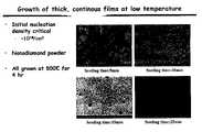
- FIG. 1illustrates the enhancement of nucleation density for the growth of nanocrystalline films grown at 500° C., and seeded using nanocrystalline diamond powder for 5 minutes; 10 minutes, 15 minutes and 25 minutes;
- FIG. 2illustrates the temperature calibration that was performed as a function of temperatures and time to determine the temperature of the substrate during deposition
- FIG. 3illustrates the visible Raman data of films deposited at substrate temperatures of 400° C. to 800° C.
- FIG. 4illustrates the NEXAFS data from diamond and graphite reference films
- FIG. 5illustrates the NEXAFS data as a function of temperature
- FIG. 6illustrates the high resolution TEM taken from a UNCD film grown at low temperature
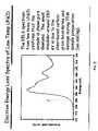
- FIG. 7illustrates Electron Energy Loss Spectra of Low Temp UNCD
- FIG. 8illustrates the grain size distribution in a 400° C. grown UNCD film
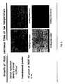
- FIG. 9illustrates the SEM of UNCD films grown at 400° C. and 800° C. and a SEM cross-section of the 400° C. film.
- FIG. 10illustrates low-temperature UNCD growth onto a CMOS chip.
- a silicon wafer 100 mm in diameterwas cleaned and seeded by immersing the wafer in an ultrasonic bath containing a mixture of nanometer sized diamond powder and an organic solvent (acetone, methanol, etc.). After the ultrasound, the wafer was removed from the bath and rinsed using a combination of organic solvent and distilled wafer.
- the seeding processwas optimized to give the maximum initial areal nucleation density possible, about 10 10 sites/cm 2 ( FIG. 1 ); however, nucleation areal densities in the range of from about 10 10 to 10 12 are satisfactory.
- the temperature of the substrate wafer during growthwas calibrated through the use of a thermocouple mounted to the surface of a test wafer which was loaded into the microwave plasma chemical vapor deposition system and exposed to the same set of process conditions as would be used to grow a film at low temperatures ( FIG. 2 ). It is not necessary to perform this step every time a low-temperature deposition is to be performed. With the substrate heater turned OFF, it was estimated that the temperature was about 318° C.+/ ⁇ 50° C. By turning the heater ON and supplying differing amount of heating current to the heater, the temperature at the wafer surface was continuously adjusted from about 320° C. to 850° C.
- the seeded silicon waferwas loaded into the plasma system, and the chamber was pumped down using vacuum pumps to a pressure of about 10-4 Torr for a period of about 30 minutes, to remove as much nitrogen gas from the deposition system prior to deposition of UNCD.
- the position of the wafer relative to the plasmawas adjusted vertically so that the wafer surface just contacted the bottom of the plasma. If the wafer position was too high, then the heating of the wafer surface by the plasma was too great, leading to both higher temperatures and non-uniform temperatures across the wafer surface. If the wafer position is too low, then no growth of UNCD will occur. Adjustment to obtain the desired substrate (wafer) temperature is within the skill of the art.
- the growth time for the inventive filmswas four hours. In practice, this time would be adjusted based on the intended application. After four hours had elapsed, the microwave power was turned off, the gas flows stopped, and then Ar gas was flowed at a high rate (400 sccm) to cool the sample rapidly. After about 30 minutes, the wafer was then removed and subjected to characterization using Raman Spectroscopy, scanning electron microscopy (SEM), high-resolution transmission electron microscopy (TEM), and near-edge x-ray absorption fine structure (NEXFAS).
- SEMscanning electron microscopy
- TEMhigh-resolution transmission electron microscopy
- NEXFASnear-edge x-ray absorption fine structure
- FIG. 3shows a series of Raman spectra obtained from films grown at different temperatures. Interpretation of these spectra is that the spectrum effectively represents the sp 2 -bonding structures within the grain boundaries only and not the grains themselves. The change in line shape between 600° C. and 700° C. indicates the role of hydrogen in the growth.
- FIGS. 4-5show the near-edge x-ray absorption spectroscopy data (NEXAFS) obtained from diamond and graphite reference samples and a series of films grown at low temperatures. These data clearly show that all of the films contain a substantial amount (greater than 90%) sp 3 (diamond) bonding.
- NXAFSnear-edge x-ray absorption spectroscopy data
- FIGS. 6-8show high-resolution transmission electron microscopy data (TEM) obtained from a low-temperature film grown at about 400° C. These data clearly indicate that the low-temperature films consist of grains 3-20 nm in size (average about 10 nm) and abrupt grain boundaries; a very similar nanoscale structure compared to UNCD films (3-5 nm) grown at 800° C.
- TEMtransmission electron microscopy data
- FIG. 10shows that we successfully grew on a silicon wafer containing microelectronic CMOS (complementary metal-oxide-semiconductor) circuits with a low-temperature UNCD film.
- CMOScomplementary metal-oxide-semiconductor
- the overarching goal of diamond thin film researchis to develop techniques and practices that allow the deposition of films on a variety of substrates that retain most if not all of the outstanding properties of natural diamond (hardness, electron mobility, thermal conductivity, etc.).
- This workhas been going on for many years and has resulted in a number of thin film deposition technologies for growing diamond (>95% sp 3 bonded carbon) films, including the patented ultrananocrystalline diamond (UNCD) technology invented by Gruen and co-workers at Argonne National Laboratory.
- the two major techniquesare plasma enhanced chemical vapor deposition (PECVD, using either RF or microwave frequencies) and hot-filament reactors.
- a crucial aspect of the current inventionis the realization that, with a few additional processing steps and the application of voltages to the sample during growth, the fundamental deposition chemistry involved in the UNCD technology developed at ANL will allow nanocrystalline diamond films to be deposited at low temperatures with deposition rates high enough so that enough film can be deposited to be useful, particularly as an anti-stiction coating in current and future MEMS devices. It is important that the films also be continuous, pinhole free, and fully dense, for applications such as electrochemical electrodes or hermetic coatings.
- the UNCD technologyinvolves the generation of C 2 -dimer molecules, which are believed to be the fundamental growth species for the synthesis of UNCD thin films.
- C 2 dimersare generated in noble-gas discharges, in which a small amount of carbon source gas is added.
- the typical plasma chemistriesuse a gas mixture of 99% Ar with 1% CH 4 .
- C 2 dimerswill naturally insert into the diamond lattice with remarkably low activation energies of 5.9 kcal/mole, which is much lower that for the more common technique used to grow diamond films, e.g. with hydrogen-methane plasmas for which methyl radicals are the principal growth species.
- the hydrogen-abstraction reactionsrequire much higher energies (25 kcal/mole) than the C 2 dimer-based chemistry that is the heart of the UNCD technology.
- any inert gasother than helium, may be used and carbon sources other than methane, such as acetylene, fullerene or anthracene may be used in some situations be preferred.
- the subject inventioninvolves the following key points:
- nanocrystalline diamond powderto seed the substrate surface prior to growth, in such a way as to maximize the areal density of initial growth sites on the surface.
- the best resultsare with nanocrystalline diamonds of less than about 20 nm average grain size but grain sizes up to about 30 nm may be used.
- nucleation sitesinitial growth initiation sites
- FIG. 1illustrates the enhancement of nucleation density on the growth of a UNCD thin film at low temperatures.
- FIG. 10A film grown at a nominal temperature of ⁇ 350° C. is shown in FIG. 10 .
- This filmwas deposited on a silicon wafer that was seeded using nanocrystalline diamond powder ultrasonically for 30 minutes prior to growth, and was grown using an initial bias voltage of ⁇ 100 V. The film was grown for four hours. After deposition, the wafer was cleaved and examined in cross-section using scanning electron microscopy (SEM). The film thickness measured is about 0.8 um. This is only slightly less than the ⁇ 1.0 ⁇ m thickness that is usually observed for UNCD films grown at 800° C. UV Raman data (not shown) indicate the clear presence of sp 3 bonding in the film.
Landscapes
- Chemical & Material Sciences (AREA)
- Engineering & Computer Science (AREA)
- Mechanical Engineering (AREA)
- Inorganic Chemistry (AREA)
- General Chemical & Material Sciences (AREA)
- Chemical Kinetics & Catalysis (AREA)
- Materials Engineering (AREA)
- Metallurgy (AREA)
- Organic Chemistry (AREA)
- Combustion & Propulsion (AREA)
- Plasma & Fusion (AREA)
- Physics & Mathematics (AREA)
- Crystals, And After-Treatments Of Crystals (AREA)
- Chemical Vapour Deposition (AREA)
Abstract
Description
Claims (16)
Priority Applications (1)
| Application Number | Priority Date | Filing Date | Title |
|---|---|---|---|
| US10/892,736US7556982B2 (en) | 2003-08-07 | 2004-07-15 | Method to grow pure nanocrystalline diamond films at low temperatures and high deposition rates |
Applications Claiming Priority (2)
| Application Number | Priority Date | Filing Date | Title |
|---|---|---|---|
| US49315203P | 2003-08-07 | 2003-08-07 | |
| US10/892,736US7556982B2 (en) | 2003-08-07 | 2004-07-15 | Method to grow pure nanocrystalline diamond films at low temperatures and high deposition rates |
Publications (2)
| Publication Number | Publication Date |
|---|---|
| US20050031785A1 US20050031785A1 (en) | 2005-02-10 |
| US7556982B2true US7556982B2 (en) | 2009-07-07 |
Family
ID=34119053
Family Applications (1)
| Application Number | Title | Priority Date | Filing Date |
|---|---|---|---|
| US10/892,736Active2026-07-08US7556982B2 (en) | 2003-08-07 | 2004-07-15 | Method to grow pure nanocrystalline diamond films at low temperatures and high deposition rates |
Country Status (1)
| Country | Link |
|---|---|
| US (1) | US7556982B2 (en) |
Cited By (9)
| Publication number | Priority date | Publication date | Assignee | Title |
|---|---|---|---|---|
| US20120199553A1 (en)* | 2004-04-19 | 2012-08-09 | Yoshinori Koga | Carbon film |
| US20130260157A1 (en)* | 2012-03-28 | 2013-10-03 | Korea Institute Of Science And Technology | Nanocrystalline diamond film and method for fabricating the same |
| US9418814B2 (en)* | 2015-01-12 | 2016-08-16 | Uchicago Argonne, Llc | Planar field emitters and high efficiency photocathodes based on ultrananocrystalline diamond |
| US9484474B1 (en)* | 2015-07-02 | 2016-11-01 | Uchicago Argonne, Llc | Ultrananocrystalline diamond contacts for electronic devices |
| US10410860B2 (en) | 2015-07-10 | 2019-09-10 | Uchicago Argonne, Llc | Transparent nanocrystalline diamond coatings and devices |
| US10662523B2 (en) | 2015-05-27 | 2020-05-26 | John Crane Inc. | Extreme durability composite diamond film |
| US10662550B2 (en) | 2016-11-03 | 2020-05-26 | John Crane Inc. | Diamond nanostructures with large surface area and method of producing the same |
| US10907264B2 (en) | 2015-06-10 | 2021-02-02 | Advanced Diamond Technologies, Inc. | Extreme durability composite diamond electrodes |
| RU2763103C1 (en)* | 2020-08-27 | 2021-12-27 | Федеральное государственное бюджетное учреждение науки Федеральный исследовательский центр "Институт общей физики им. А.М. Прохорова Российской академии наук" (ИОФ РАН) | Method for monitoring and controlling the temperature regime of the growth surface of the substrate |
Families Citing this family (24)
| Publication number | Priority date | Publication date | Assignee | Title |
|---|---|---|---|---|
| US7589029B2 (en) | 2002-05-02 | 2009-09-15 | Micron Technology, Inc. | Atomic layer deposition and conversion |
| US7122837B2 (en)* | 2005-01-11 | 2006-10-17 | Apollo Diamond, Inc | Structures formed in diamond |
| US7829377B2 (en)* | 2005-01-11 | 2010-11-09 | Apollo Diamond, Inc | Diamond medical devices |
| US7927948B2 (en) | 2005-07-20 | 2011-04-19 | Micron Technology, Inc. | Devices with nanocrystals and methods of formation |
| US7989290B2 (en)* | 2005-08-04 | 2011-08-02 | Micron Technology, Inc. | Methods for forming rhodium-based charge traps and apparatus including rhodium-based charge traps |
| US7575978B2 (en)* | 2005-08-04 | 2009-08-18 | Micron Technology, Inc. | Method for making conductive nanoparticle charge storage element |
| US20070205521A1 (en)* | 2006-01-27 | 2007-09-06 | Lockheed Martin Corporation | Encapsulation of Semiconductor Components |
| US20110107473A1 (en)* | 2006-03-15 | 2011-05-05 | Wisconsin Alumni Research Foundation | Diamond-like carbon coated nanoprobes |
| US7947329B2 (en)* | 2006-09-11 | 2011-05-24 | Wisconsin Alumni Research Foundation | Methods of applying a nanocrystalline diamond film to a cutting tool |
| KR100924287B1 (en)* | 2007-05-10 | 2009-10-30 | 한국과학기술연구원 | DC power plasma deposition apparatus that does not have a positive pole, the material deposition method without the positive pole and the diamond thin film produced thereby |
| US8367506B2 (en) | 2007-06-04 | 2013-02-05 | Micron Technology, Inc. | High-k dielectrics with gold nano-particles |
| US20090017258A1 (en)* | 2007-07-10 | 2009-01-15 | Carlisle John A | Diamond film deposition |
| US8197701B2 (en)* | 2007-07-13 | 2012-06-12 | Advanced Diamond Technologies, Inc. | Diamond film deposition and probes |
| US8227350B2 (en)* | 2008-01-04 | 2012-07-24 | Advanced Diamond Technologies, Inc. | Controlling diamond film surfaces and layering |
| US20090214826A1 (en)* | 2008-01-04 | 2009-08-27 | Charles West | Controlling diamond film surfaces |
| GB201121655D0 (en)* | 2011-12-16 | 2012-01-25 | Element Six Ltd | Substrates for semiconductor devices |
| CN103985496B (en)* | 2014-05-27 | 2017-07-28 | 江西科技师范大学 | A kind of magnetic Nano diamond particles material and its preparation method and application |
| CN106910713B (en)* | 2015-12-22 | 2020-08-04 | 中芯国际集成电路制造(北京)有限公司 | Semiconductor device and method of manufacturing the same |
| US10760157B2 (en)* | 2016-08-09 | 2020-09-01 | Akhan Semiconductor, Inc. | Thin film diamond coating system and method |
| CN107955929B (en)* | 2017-12-20 | 2020-04-17 | 四川纳涂科技有限公司 | Surface boronizing modification method for high-cobalt hard alloy die |
| US11637068B2 (en) | 2020-12-15 | 2023-04-25 | Globalfoundries U.S. Inc. | Thermally and electrically conductive interconnects |
| WO2022185098A1 (en) | 2021-03-04 | 2022-09-09 | Crystallyte Co., Ltd. | Electrolytic process for producing a nanocrystalline carbon with 1 d, 2d, or 3d structure and/or a nanocrystalline diamond and/or an amorphous carbon and/or a metal-carbon nanomaterial composite and/or a mixture thereof at ambient conditions |
| US11901304B2 (en) | 2021-05-18 | 2024-02-13 | Globalfoundries U.S. Inc. | Integrated circuit structure with fluorescent material, and related methods |
| CN115896741A (en)* | 2022-12-30 | 2023-04-04 | 重庆启石元素科技发展有限公司 | Growth method of large-size diamond wafer |
Citations (11)
| Publication number | Priority date | Publication date | Assignee | Title |
|---|---|---|---|---|
| US5149381A (en)* | 1987-12-04 | 1992-09-22 | Fried.Krupp Gmbh | Method of making a composite powder comprising nanocrystallites embedded in an amorphous phase |
| US5698328A (en)* | 1994-04-06 | 1997-12-16 | The Regents Of The University Of California | Diamond thin film electron emitter |
| US5772760A (en)* | 1991-11-25 | 1998-06-30 | The University Of Chicago | Method for the preparation of nanocrystalline diamond thin films |
| US5954147A (en)* | 1997-07-09 | 1999-09-21 | Baker Hughes Incorporated | Earth boring bits with nanocrystalline diamond enhanced elements |
| US5989511A (en)* | 1991-11-25 | 1999-11-23 | The University Of Chicago | Smooth diamond films as low friction, long wear surfaces |
| US6586797B2 (en)* | 2001-08-30 | 2003-07-01 | Micron Technology, Inc. | Graded composition gate insulators to reduce tunneling barriers in flash memory devices |
| US20030152700A1 (en)* | 2002-02-11 | 2003-08-14 | Board Of Trustees Operating Michigan State University | Process for synthesizing uniform nanocrystalline films |
| US6667215B2 (en)* | 2002-05-02 | 2003-12-23 | 3M Innovative Properties | Method of making transistors |
| US6746893B1 (en)* | 1997-07-29 | 2004-06-08 | Micron Technology, Inc. | Transistor with variable electron affinity gate and methods of fabrication and use |
| US20050042161A1 (en) | 2003-06-26 | 2005-02-24 | The University Of Chicago | Method to grow carbon thin films consisting entirely of diamond grains 3-5 nm in size and high-energy grain boundaries |
| US20070020403A1 (en)* | 2003-05-30 | 2007-01-25 | Japan Science And Technology Agency | Process for producing extremely flat microcrystalline diamond thin film by laser ablation method |
- 2004
- 2004-07-15USUS10/892,736patent/US7556982B2/enactiveActive
Patent Citations (11)
| Publication number | Priority date | Publication date | Assignee | Title |
|---|---|---|---|---|
| US5149381A (en)* | 1987-12-04 | 1992-09-22 | Fried.Krupp Gmbh | Method of making a composite powder comprising nanocrystallites embedded in an amorphous phase |
| US5772760A (en)* | 1991-11-25 | 1998-06-30 | The University Of Chicago | Method for the preparation of nanocrystalline diamond thin films |
| US5989511A (en)* | 1991-11-25 | 1999-11-23 | The University Of Chicago | Smooth diamond films as low friction, long wear surfaces |
| US5698328A (en)* | 1994-04-06 | 1997-12-16 | The Regents Of The University Of California | Diamond thin film electron emitter |
| US5954147A (en)* | 1997-07-09 | 1999-09-21 | Baker Hughes Incorporated | Earth boring bits with nanocrystalline diamond enhanced elements |
| US6746893B1 (en)* | 1997-07-29 | 2004-06-08 | Micron Technology, Inc. | Transistor with variable electron affinity gate and methods of fabrication and use |
| US6586797B2 (en)* | 2001-08-30 | 2003-07-01 | Micron Technology, Inc. | Graded composition gate insulators to reduce tunneling barriers in flash memory devices |
| US20030152700A1 (en)* | 2002-02-11 | 2003-08-14 | Board Of Trustees Operating Michigan State University | Process for synthesizing uniform nanocrystalline films |
| US6667215B2 (en)* | 2002-05-02 | 2003-12-23 | 3M Innovative Properties | Method of making transistors |
| US20070020403A1 (en)* | 2003-05-30 | 2007-01-25 | Japan Science And Technology Agency | Process for producing extremely flat microcrystalline diamond thin film by laser ablation method |
| US20050042161A1 (en) | 2003-06-26 | 2005-02-24 | The University Of Chicago | Method to grow carbon thin films consisting entirely of diamond grains 3-5 nm in size and high-energy grain boundaries |
Cited By (12)
| Publication number | Priority date | Publication date | Assignee | Title |
|---|---|---|---|---|
| US20120199553A1 (en)* | 2004-04-19 | 2012-08-09 | Yoshinori Koga | Carbon film |
| US8501276B2 (en)* | 2004-04-19 | 2013-08-06 | National Institute Of Advanced Industrial Science And Technology | Carbon film |
| US20130260157A1 (en)* | 2012-03-28 | 2013-10-03 | Korea Institute Of Science And Technology | Nanocrystalline diamond film and method for fabricating the same |
| US9074281B2 (en)* | 2012-03-28 | 2015-07-07 | Korea Institute Of Science And Technology | Methods for fabricating nanocrystalline diamond film |
| US9418814B2 (en)* | 2015-01-12 | 2016-08-16 | Uchicago Argonne, Llc | Planar field emitters and high efficiency photocathodes based on ultrananocrystalline diamond |
| US10662523B2 (en) | 2015-05-27 | 2020-05-26 | John Crane Inc. | Extreme durability composite diamond film |
| US10907264B2 (en) | 2015-06-10 | 2021-02-02 | Advanced Diamond Technologies, Inc. | Extreme durability composite diamond electrodes |
| US9484474B1 (en)* | 2015-07-02 | 2016-11-01 | Uchicago Argonne, Llc | Ultrananocrystalline diamond contacts for electronic devices |
| US9842958B2 (en) | 2015-07-02 | 2017-12-12 | Uchicago Argonne, Llc | Ultrananocrystalline diamond contacts for electronic devices |
| US10410860B2 (en) | 2015-07-10 | 2019-09-10 | Uchicago Argonne, Llc | Transparent nanocrystalline diamond coatings and devices |
| US10662550B2 (en) | 2016-11-03 | 2020-05-26 | John Crane Inc. | Diamond nanostructures with large surface area and method of producing the same |
| RU2763103C1 (en)* | 2020-08-27 | 2021-12-27 | Федеральное государственное бюджетное учреждение науки Федеральный исследовательский центр "Институт общей физики им. А.М. Прохорова Российской академии наук" (ИОФ РАН) | Method for monitoring and controlling the temperature regime of the growth surface of the substrate |
Also Published As
| Publication number | Publication date |
|---|---|
| US20050031785A1 (en) | 2005-02-10 |
Similar Documents
| Publication | Publication Date | Title |
|---|---|---|
| US7556982B2 (en) | Method to grow pure nanocrystalline diamond films at low temperatures and high deposition rates | |
| US5814149A (en) | Methods for manufacturing monocrystalline diamond films | |
| EP0365366B1 (en) | Continuous thin diamond film and method for making same | |
| US5432003A (en) | Continuous thin diamond film and method for making same | |
| US20090017258A1 (en) | Diamond film deposition | |
| US8158011B2 (en) | Method of fabrication of cubic boron nitride conical microstructures | |
| Feng et al. | Effect of graphitic carbon films on diamond nucleation by microwave‐plasma‐enhanced chemical‐vapor deposition | |
| Stubhan et al. | Heteroepitaxial nucleation of diamond on Si (001) in hot filament chemical vapor deposition | |
| US5471947A (en) | Preparation of diamond films on silicon substrates | |
| Sharda et al. | High compressive stress in nanocrystalline diamond films grown by microwave plasma chemical vapor deposition | |
| JPH0948693A (en) | Method for forming diamond single crystal film | |
| US5358754A (en) | Method for forming diamond films by vapor phase synthesis | |
| US5200231A (en) | Method of manufacturing polycrystalline diamond layers | |
| US20040079280A1 (en) | Fabrication of single crystal diamond tips and their arrays | |
| Piazza et al. | Synthesis of diamond at sub 300 C substrate temperature | |
| Rotter et al. | Diamond CVD by a combined plasma pretreatment and seeding procedure | |
| Corrigan et al. | Low temperature growth of ultra-nanocrystalline diamond on glass substrates for field emission applications | |
| Kang et al. | Diamond nucleation and growth under very low-pressure conditions | |
| Friedbacher et al. | Pretreatment of silicon substrates for CVD diamond deposition studied by atomic force microscopy | |
| US20250109488A1 (en) | Method for growing diamond on silicon substrate and method for selectively growing diamond on silicon substrate | |
| GB2270326A (en) | Growth of diamond films on silicon substrates with application of bias to substrate; tessellated patterns | |
| JP2001226194A (en) | Low-temperature deposition method and apparatus for microcrystalline diamond thin film | |
| Li et al. | Diamond nucleation on singlecrystalline 6H-SiC substrates by bias-enhanced nucleation in hot filament chemical vapor deposition | |
| Khan et al. | Nanodiamond: synthesis, transport property, field emission and applications | |
| Sun et al. | Diamond film growth on the carbon films from electrolysis of ethanol |
Legal Events
| Date | Code | Title | Description |
|---|---|---|---|
| AS | Assignment | Owner name:ENERGY, UNITED STATES DEPARTMENT OF, DISTRICT OF C Free format text:CONFIRMATORY LICENSE;ASSIGNOR:CHICAGO, UNIVERSITY OF THE;REEL/FRAME:016048/0792 Effective date:20041122 | |
| AS | Assignment | Owner name:THE UNIVERSITY OF CHICAGO, ILLINOIS Free format text:ASSIGNMENT OF ASSIGNORS INTEREST;ASSIGNORS:CARLISLE, JOHN A.;GRUEN, DIETER M.;AUCIELLO, ORLANDO;AND OTHERS;REEL/FRAME:015575/0458 Effective date:20040714 | |
| AS | Assignment | Owner name:U CHICAGO ARGONNE LLC,ILLINOIS Free format text:ASSIGNMENT OF ASSIGNORS INTEREST;ASSIGNOR:UNIVERSITY OF CHICAGO, THE;REEL/FRAME:018385/0618 Effective date:20060925 Owner name:U CHICAGO ARGONNE LLC, ILLINOIS Free format text:ASSIGNMENT OF ASSIGNORS INTEREST;ASSIGNOR:UNIVERSITY OF CHICAGO, THE;REEL/FRAME:018385/0618 Effective date:20060925 | |
| STCF | Information on status: patent grant | Free format text:PATENTED CASE | |
| FEPP | Fee payment procedure | Free format text:PAYER NUMBER DE-ASSIGNED (ORIGINAL EVENT CODE: RMPN); ENTITY STATUS OF PATENT OWNER: SMALL ENTITY Free format text:PAYOR NUMBER ASSIGNED (ORIGINAL EVENT CODE: ASPN); ENTITY STATUS OF PATENT OWNER: SMALL ENTITY | |
| FPAY | Fee payment | Year of fee payment:4 | |
| SULP | Surcharge for late payment | ||
| FPAY | Fee payment | Year of fee payment:8 | |
| MAFP | Maintenance fee payment | Free format text:PAYMENT OF MAINTENANCE FEE, 12TH YR, SMALL ENTITY (ORIGINAL EVENT CODE: M2553); ENTITY STATUS OF PATENT OWNER: SMALL ENTITY Year of fee payment:12 |