US7555333B2 - Integrated optical scanning image acquisition and display - Google Patents
Integrated optical scanning image acquisition and displayDownload PDFInfo
- Publication number
- US7555333B2 US7555333B2US10/655,482US65548203AUS7555333B2US 7555333 B2US7555333 B2US 7555333B2US 65548203 AUS65548203 AUS 65548203AUS 7555333 B2US7555333 B2US 7555333B2
- Authority
- US
- United States
- Prior art keywords
- cantilever
- light
- free end
- actuator
- substrate
- Prior art date
- Legal status (The legal status is an assumption and is not a legal conclusion. Google has not performed a legal analysis and makes no representation as to the accuracy of the status listed.)
- Expired - Fee Related, expires
Links
- 230000003287optical effectEffects0.000titleclaimsdescription53
- 239000000758substrateSubstances0.000claimsabstractdescription69
- 238000000034methodMethods0.000claimsabstractdescription48
- 230000033001locomotionEffects0.000claimsdescription31
- 239000013307optical fiberSubstances0.000claimsdescription26
- 238000006073displacement reactionMethods0.000claimsdescription25
- 239000010409thin filmSubstances0.000claimsdescription24
- 239000000463materialSubstances0.000claimsdescription23
- 239000000835fiberSubstances0.000claimsdescription19
- VYPSYNLAJGMNEJ-UHFFFAOYSA-NSilicium dioxideChemical compoundO=[Si]=OVYPSYNLAJGMNEJ-UHFFFAOYSA-N0.000claimsdescription12
- 229910052814silicon oxideInorganic materials0.000claimsdescription11
- 238000001514detection methodMethods0.000claimsdescription10
- 230000008878couplingEffects0.000claimsdescription9
- 238000010168coupling processMethods0.000claimsdescription9
- 238000005859coupling reactionMethods0.000claimsdescription9
- 238000005452bendingMethods0.000claimsdescription7
- 230000005291magnetic effectEffects0.000claimsdescription6
- 229910052581Si3N4Inorganic materials0.000claimsdescription5
- 238000000708deep reactive-ion etchingMethods0.000claimsdescription5
- 239000010408filmSubstances0.000claimsdescription5
- HQVNEWCFYHHQES-UHFFFAOYSA-Nsilicon nitrideChemical compoundN12[Si]34N5[Si]62N3[Si]51N64HQVNEWCFYHHQES-UHFFFAOYSA-N0.000claimsdescription5
- 239000003822epoxy resinSubstances0.000claimsdescription4
- 230000001939inductive effectEffects0.000claimsdescription4
- 229920000647polyepoxidePolymers0.000claimsdescription4
- 238000001228spectrumMethods0.000claimsdescription4
- 239000011521glassSubstances0.000claimsdescription3
- 229920002120photoresistant polymerPolymers0.000claimsdescription3
- 238000000347anisotropic wet etchingMethods0.000claims3
- 238000000609electron-beam lithographyMethods0.000claims2
- 238000000206photolithographyMethods0.000claims2
- 229920000642polymerPolymers0.000claims2
- 230000006870functionEffects0.000abstractdescription25
- 238000002560therapeutic procedureMethods0.000abstractdescription18
- 238000004519manufacturing processMethods0.000abstractdescription14
- 229920005989resinPolymers0.000abstractdescription2
- 239000011347resinSubstances0.000abstractdescription2
- 238000003384imaging methodMethods0.000description32
- XUIMIQQOPSSXEZ-UHFFFAOYSA-NSiliconChemical compound[Si]XUIMIQQOPSSXEZ-UHFFFAOYSA-N0.000description25
- 229910052710siliconInorganic materials0.000description25
- 239000010703siliconSubstances0.000description25
- 238000005286illuminationMethods0.000description16
- 229920001486SU-8 photoresistPolymers0.000description14
- 238000012545processingMethods0.000description14
- 238000013459approachMethods0.000description10
- 230000000694effectsEffects0.000description10
- 230000001965increasing effectEffects0.000description9
- 230000001225therapeutic effectEffects0.000description9
- 230000008901benefitEffects0.000description8
- 238000012544monitoring processMethods0.000description8
- 229910052796boronInorganic materials0.000description6
- 230000008859changeEffects0.000description6
- 229910052451lead zirconate titanateInorganic materials0.000description6
- 230000008569processEffects0.000description6
- ZOXJGFHDIHLPTG-UHFFFAOYSA-NBoronChemical compound[B]ZOXJGFHDIHLPTG-UHFFFAOYSA-N0.000description5
- 239000002033PVDF binderSubstances0.000description5
- 230000005540biological transmissionEffects0.000description5
- 230000005284excitationEffects0.000description5
- 230000007246mechanismEffects0.000description5
- 238000012634optical imagingMethods0.000description5
- 229920002981polyvinylidene fluoridePolymers0.000description5
- 239000000523sampleSubstances0.000description5
- 239000004065semiconductorSubstances0.000description5
- 238000013500data storageMethods0.000description4
- 238000013461designMethods0.000description4
- 238000009792diffusion processMethods0.000description4
- 238000005516engineering processMethods0.000description4
- 229910052782aluminiumInorganic materials0.000description3
- 230000003139buffering effectEffects0.000description3
- 238000006243chemical reactionMethods0.000description3
- 239000002131composite materialSubstances0.000description3
- 238000000151depositionMethods0.000description3
- 238000003745diagnosisMethods0.000description3
- 238000001914filtrationMethods0.000description3
- 229910052751metalInorganic materials0.000description3
- 239000002184metalSubstances0.000description3
- 230000004044responseEffects0.000description3
- 239000000126substanceSubstances0.000description3
- 229910020776SixNyInorganic materials0.000description2
- 238000010521absorption reactionMethods0.000description2
- 230000003321amplificationEffects0.000description2
- 230000009286beneficial effectEffects0.000description2
- 238000004891communicationMethods0.000description2
- 238000005520cutting processMethods0.000description2
- 238000002059diagnostic imagingMethods0.000description2
- 238000010586diagramMethods0.000description2
- 239000002019doping agentSubstances0.000description2
- 230000009977dual effectEffects0.000description2
- 230000005684electric fieldEffects0.000description2
- 230000007613environmental effectEffects0.000description2
- 238000005530etchingMethods0.000description2
- 229910052737goldInorganic materials0.000description2
- 230000036541healthEffects0.000description2
- 230000010354integrationEffects0.000description2
- 239000007788liquidSubstances0.000description2
- 230000007774longtermEffects0.000description2
- 238000005259measurementMethods0.000description2
- 238000012986modificationMethods0.000description2
- 230000004048modificationEffects0.000description2
- 238000004651near-field scanning optical microscopyMethods0.000description2
- 238000003199nucleic acid amplification methodMethods0.000description2
- 238000000399optical microscopyMethods0.000description2
- 238000002428photodynamic therapyMethods0.000description2
- 238000001020plasma etchingMethods0.000description2
- 230000010287polarizationEffects0.000description2
- 230000009467reductionEffects0.000description2
- 238000009877renderingMethods0.000description2
- 230000002441reversible effectEffects0.000description2
- 238000005070samplingMethods0.000description2
- 238000004544sputter depositionMethods0.000description2
- 230000000087stabilizing effectEffects0.000description2
- 230000035882stressEffects0.000description2
- 230000000451tissue damageEffects0.000description2
- 231100000827tissue damageToxicity0.000description2
- 238000012549trainingMethods0.000description2
- 230000000007visual effectEffects0.000description2
- 229910052582BNInorganic materials0.000description1
- PZNSFCLAULLKQX-UHFFFAOYSA-NBoron nitrideChemical compoundN#BPZNSFCLAULLKQX-UHFFFAOYSA-N0.000description1
- 239000004593EpoxySubstances0.000description1
- 229910001218Gallium arsenideInorganic materials0.000description1
- 206010028980NeoplasmDiseases0.000description1
- 239000000853adhesiveSubstances0.000description1
- 230000001070adhesive effectEffects0.000description1
- XAGFODPZIPBFFR-UHFFFAOYSA-NaluminiumChemical compound[Al]XAGFODPZIPBFFR-UHFFFAOYSA-N0.000description1
- 230000002457bidirectional effectEffects0.000description1
- 238000001574biopsyMethods0.000description1
- -1boron ionChemical class0.000description1
- 230000015556catabolic processEffects0.000description1
- 229910052804chromiumInorganic materials0.000description1
- 238000005253claddingMethods0.000description1
- 150000001875compoundsChemical class0.000description1
- 239000004020conductorSubstances0.000description1
- 238000010276constructionMethods0.000description1
- 229910052802copperInorganic materials0.000description1
- 239000013078crystalSubstances0.000description1
- 230000006378damageEffects0.000description1
- 230000007423decreaseEffects0.000description1
- 230000023077detection of light stimulusEffects0.000description1
- 238000011161developmentMethods0.000description1
- 238000000295emission spectrumMethods0.000description1
- 239000003302ferromagnetic materialSubstances0.000description1
- 230000005669field effectEffects0.000description1
- 239000013305flexible fiberSubstances0.000description1
- 239000012530fluidSubstances0.000description1
- 239000007850fluorescent dyeSubstances0.000description1
- 239000005350fused silica glassSubstances0.000description1
- 238000010438heat treatmentMethods0.000description1
- 238000002847impedance measurementMethods0.000description1
- 239000012535impuritySubstances0.000description1
- 208000014674injuryDiseases0.000description1
- 238000007689inspectionMethods0.000description1
- 230000002452interceptive effectEffects0.000description1
- 238000002647laser therapyMethods0.000description1
- HFGPZNIAWCZYJU-UHFFFAOYSA-Nlead zirconate titanateChemical compound[O-2].[O-2].[O-2].[O-2].[O-2].[Ti+4].[Zr+4].[Pb+2]HFGPZNIAWCZYJU-UHFFFAOYSA-N0.000description1
- WABPQHHGFIMREM-AHCXROLUSA-Nlead-203Chemical compound[203Pb]WABPQHHGFIMREM-AHCXROLUSA-N0.000description1
- 238000003754machiningMethods0.000description1
- 150000002739metalsChemical class0.000description1
- 238000001393microlithographyMethods0.000description1
- 238000001053micromouldingMethods0.000description1
- 229910021421monocrystalline siliconInorganic materials0.000description1
- 229910052697platinumInorganic materials0.000description1
- 239000000843powderSubstances0.000description1
- 238000011084recoveryMethods0.000description1
- 230000004043responsivenessEffects0.000description1
- 230000035945sensitivityEffects0.000description1
- 238000000926separation methodMethods0.000description1
- LIVNPJMFVYWSIS-UHFFFAOYSA-Nsilicon monoxideChemical compound[Si-]#[O+]LIVNPJMFVYWSIS-UHFFFAOYSA-N0.000description1
- 229920002379silicone rubberPolymers0.000description1
- 239000004945silicone rubberSubstances0.000description1
- 229910052709silverInorganic materials0.000description1
- 238000004513sizingMethods0.000description1
- 238000003980solgel methodMethods0.000description1
- 239000007787solidSubstances0.000description1
- 238000004528spin coatingMethods0.000description1
- 230000002269spontaneous effectEffects0.000description1
- 238000001356surgical procedureMethods0.000description1
- 230000008961swellingEffects0.000description1
- 238000012360testing methodMethods0.000description1
- 230000008646thermal stressEffects0.000description1
- 238000000427thin-film depositionMethods0.000description1
- 230000008733traumaEffects0.000description1
- 238000001429visible spectrumMethods0.000description1
- 238000009736wettingMethods0.000description1
Images


Classifications
- A—HUMAN NECESSITIES
- A61—MEDICAL OR VETERINARY SCIENCE; HYGIENE
- A61B—DIAGNOSIS; SURGERY; IDENTIFICATION
- A61B5/00—Measuring for diagnostic purposes; Identification of persons
- A61B5/0059—Measuring for diagnostic purposes; Identification of persons using light, e.g. diagnosis by transillumination, diascopy, fluorescence
- A61B5/0062—Arrangements for scanning
- A—HUMAN NECESSITIES
- A61—MEDICAL OR VETERINARY SCIENCE; HYGIENE
- A61B—DIAGNOSIS; SURGERY; IDENTIFICATION
- A61B1/00—Instruments for performing medical examinations of the interior of cavities or tubes of the body by visual or photographical inspection, e.g. endoscopes; Illuminating arrangements therefor
- A61B1/00002—Operational features of endoscopes
- A61B1/00043—Operational features of endoscopes provided with output arrangements
- A61B1/00045—Display arrangement
- A61B1/00048—Constructional features of the display
- A—HUMAN NECESSITIES
- A61—MEDICAL OR VETERINARY SCIENCE; HYGIENE
- A61B—DIAGNOSIS; SURGERY; IDENTIFICATION
- A61B1/00—Instruments for performing medical examinations of the interior of cavities or tubes of the body by visual or photographical inspection, e.g. endoscopes; Illuminating arrangements therefor
- A61B1/00064—Constructional details of the endoscope body
- A61B1/00071—Insertion part of the endoscope body
- A61B1/0008—Insertion part of the endoscope body characterised by distal tip features
- A—HUMAN NECESSITIES
- A61—MEDICAL OR VETERINARY SCIENCE; HYGIENE
- A61B—DIAGNOSIS; SURGERY; IDENTIFICATION
- A61B1/00—Instruments for performing medical examinations of the interior of cavities or tubes of the body by visual or photographical inspection, e.g. endoscopes; Illuminating arrangements therefor
- A61B1/00163—Optical arrangements
- A61B1/00165—Optical arrangements with light-conductive means, e.g. fibre optics
- A61B1/00167—Details of optical fibre bundles, e.g. shape or fibre distribution
- A—HUMAN NECESSITIES
- A61—MEDICAL OR VETERINARY SCIENCE; HYGIENE
- A61B—DIAGNOSIS; SURGERY; IDENTIFICATION
- A61B1/00—Instruments for performing medical examinations of the interior of cavities or tubes of the body by visual or photographical inspection, e.g. endoscopes; Illuminating arrangements therefor
- A61B1/00163—Optical arrangements
- A61B1/00172—Optical arrangements with means for scanning
- A—HUMAN NECESSITIES
- A61—MEDICAL OR VETERINARY SCIENCE; HYGIENE
- A61B—DIAGNOSIS; SURGERY; IDENTIFICATION
- A61B1/00—Instruments for performing medical examinations of the interior of cavities or tubes of the body by visual or photographical inspection, e.g. endoscopes; Illuminating arrangements therefor
- A61B1/00163—Optical arrangements
- A61B1/00174—Optical arrangements characterised by the viewing angles
- A61B1/00183—Optical arrangements characterised by the viewing angles for variable viewing angles
- A—HUMAN NECESSITIES
- A61—MEDICAL OR VETERINARY SCIENCE; HYGIENE
- A61B—DIAGNOSIS; SURGERY; IDENTIFICATION
- A61B1/00—Instruments for performing medical examinations of the interior of cavities or tubes of the body by visual or photographical inspection, e.g. endoscopes; Illuminating arrangements therefor
- A61B1/005—Flexible endoscopes
- A61B1/0051—Flexible endoscopes with controlled bending of insertion part
- A—HUMAN NECESSITIES
- A61—MEDICAL OR VETERINARY SCIENCE; HYGIENE
- A61B—DIAGNOSIS; SURGERY; IDENTIFICATION
- A61B1/00—Instruments for performing medical examinations of the interior of cavities or tubes of the body by visual or photographical inspection, e.g. endoscopes; Illuminating arrangements therefor
- A61B1/06—Instruments for performing medical examinations of the interior of cavities or tubes of the body by visual or photographical inspection, e.g. endoscopes; Illuminating arrangements therefor with illuminating arrangements
- A61B1/0638—Instruments for performing medical examinations of the interior of cavities or tubes of the body by visual or photographical inspection, e.g. endoscopes; Illuminating arrangements therefor with illuminating arrangements providing two or more wavelengths
- A—HUMAN NECESSITIES
- A61—MEDICAL OR VETERINARY SCIENCE; HYGIENE
- A61B—DIAGNOSIS; SURGERY; IDENTIFICATION
- A61B1/00—Instruments for performing medical examinations of the interior of cavities or tubes of the body by visual or photographical inspection, e.g. endoscopes; Illuminating arrangements therefor
- A61B1/06—Instruments for performing medical examinations of the interior of cavities or tubes of the body by visual or photographical inspection, e.g. endoscopes; Illuminating arrangements therefor with illuminating arrangements
- A61B1/0655—Control therefor
- A—HUMAN NECESSITIES
- A61—MEDICAL OR VETERINARY SCIENCE; HYGIENE
- A61B—DIAGNOSIS; SURGERY; IDENTIFICATION
- A61B5/00—Measuring for diagnostic purposes; Identification of persons
- A61B5/0059—Measuring for diagnostic purposes; Identification of persons using light, e.g. diagnosis by transillumination, diascopy, fluorescence
- A61B5/0082—Measuring for diagnostic purposes; Identification of persons using light, e.g. diagnosis by transillumination, diascopy, fluorescence adapted for particular medical purposes
- A61B5/0084—Measuring for diagnostic purposes; Identification of persons using light, e.g. diagnosis by transillumination, diascopy, fluorescence adapted for particular medical purposes for introduction into the body, e.g. by catheters
- G—PHYSICS
- G02—OPTICS
- G02B—OPTICAL ELEMENTS, SYSTEMS OR APPARATUS
- G02B26/00—Optical devices or arrangements for the control of light using movable or deformable optical elements
- G02B26/08—Optical devices or arrangements for the control of light using movable or deformable optical elements for controlling the direction of light
- G02B26/0875—Optical devices or arrangements for the control of light using movable or deformable optical elements for controlling the direction of light by means of one or more refracting elements
- G—PHYSICS
- G02—OPTICS
- G02B—OPTICAL ELEMENTS, SYSTEMS OR APPARATUS
- G02B26/00—Optical devices or arrangements for the control of light using movable or deformable optical elements
- G02B26/08—Optical devices or arrangements for the control of light using movable or deformable optical elements for controlling the direction of light
- G02B26/10—Scanning systems
- G02B26/101—Scanning systems with both horizontal and vertical deflecting means, e.g. raster or XY scanners
- G—PHYSICS
- G02—OPTICS
- G02B—OPTICAL ELEMENTS, SYSTEMS OR APPARATUS
- G02B6/00—Light guides; Structural details of arrangements comprising light guides and other optical elements, e.g. couplings
- G02B6/24—Coupling light guides
- G02B6/26—Optical coupling means
- G02B6/262—Optical details of coupling light into, or out of, or between fibre ends, e.g. special fibre end shapes or associated optical elements
- A—HUMAN NECESSITIES
- A61—MEDICAL OR VETERINARY SCIENCE; HYGIENE
- A61B—DIAGNOSIS; SURGERY; IDENTIFICATION
- A61B1/00—Instruments for performing medical examinations of the interior of cavities or tubes of the body by visual or photographical inspection, e.g. endoscopes; Illuminating arrangements therefor
- A61B1/00163—Optical arrangements
- A61B1/00193—Optical arrangements adapted for stereoscopic vision
- A—HUMAN NECESSITIES
- A61—MEDICAL OR VETERINARY SCIENCE; HYGIENE
- A61B—DIAGNOSIS; SURGERY; IDENTIFICATION
- A61B1/00—Instruments for performing medical examinations of the interior of cavities or tubes of the body by visual or photographical inspection, e.g. endoscopes; Illuminating arrangements therefor
- A61B1/04—Instruments for performing medical examinations of the interior of cavities or tubes of the body by visual or photographical inspection, e.g. endoscopes; Illuminating arrangements therefor combined with photographic or television appliances
- A61B1/043—Instruments for performing medical examinations of the interior of cavities or tubes of the body by visual or photographical inspection, e.g. endoscopes; Illuminating arrangements therefor combined with photographic or television appliances for fluorescence imaging
- A—HUMAN NECESSITIES
- A61—MEDICAL OR VETERINARY SCIENCE; HYGIENE
- A61B—DIAGNOSIS; SURGERY; IDENTIFICATION
- A61B1/00—Instruments for performing medical examinations of the interior of cavities or tubes of the body by visual or photographical inspection, e.g. endoscopes; Illuminating arrangements therefor
- A61B1/06—Instruments for performing medical examinations of the interior of cavities or tubes of the body by visual or photographical inspection, e.g. endoscopes; Illuminating arrangements therefor with illuminating arrangements
- A61B1/063—Instruments for performing medical examinations of the interior of cavities or tubes of the body by visual or photographical inspection, e.g. endoscopes; Illuminating arrangements therefor with illuminating arrangements for monochromatic or narrow-band illumination
- A—HUMAN NECESSITIES
- A61—MEDICAL OR VETERINARY SCIENCE; HYGIENE
- A61B—DIAGNOSIS; SURGERY; IDENTIFICATION
- A61B5/00—Measuring for diagnostic purposes; Identification of persons
- A61B5/0059—Measuring for diagnostic purposes; Identification of persons using light, e.g. diagnosis by transillumination, diascopy, fluorescence
- A61B5/0062—Arrangements for scanning
- A61B5/0066—Optical coherence imaging
- A—HUMAN NECESSITIES
- A61—MEDICAL OR VETERINARY SCIENCE; HYGIENE
- A61B—DIAGNOSIS; SURGERY; IDENTIFICATION
- A61B5/00—Measuring for diagnostic purposes; Identification of persons
- A61B5/0059—Measuring for diagnostic purposes; Identification of persons using light, e.g. diagnosis by transillumination, diascopy, fluorescence
- A61B5/0062—Arrangements for scanning
- A61B5/0068—Confocal scanning
- A—HUMAN NECESSITIES
- A61—MEDICAL OR VETERINARY SCIENCE; HYGIENE
- A61B—DIAGNOSIS; SURGERY; IDENTIFICATION
- A61B5/00—Measuring for diagnostic purposes; Identification of persons
- A61B5/0059—Measuring for diagnostic purposes; Identification of persons using light, e.g. diagnosis by transillumination, diascopy, fluorescence
- A61B5/0071—Measuring for diagnostic purposes; Identification of persons using light, e.g. diagnosis by transillumination, diascopy, fluorescence by measuring fluorescence emission
- A—HUMAN NECESSITIES
- A61—MEDICAL OR VETERINARY SCIENCE; HYGIENE
- A61B—DIAGNOSIS; SURGERY; IDENTIFICATION
- A61B5/00—Measuring for diagnostic purposes; Identification of persons
- A61B5/0059—Measuring for diagnostic purposes; Identification of persons using light, e.g. diagnosis by transillumination, diascopy, fluorescence
- A61B5/0075—Measuring for diagnostic purposes; Identification of persons using light, e.g. diagnosis by transillumination, diascopy, fluorescence by spectroscopy, i.e. measuring spectra, e.g. Raman spectroscopy, infrared absorption spectroscopy
- A—HUMAN NECESSITIES
- A61—MEDICAL OR VETERINARY SCIENCE; HYGIENE
- A61B—DIAGNOSIS; SURGERY; IDENTIFICATION
- A61B5/00—Measuring for diagnostic purposes; Identification of persons
- A61B5/0059—Measuring for diagnostic purposes; Identification of persons using light, e.g. diagnosis by transillumination, diascopy, fluorescence
- A61B5/0082—Measuring for diagnostic purposes; Identification of persons using light, e.g. diagnosis by transillumination, diascopy, fluorescence adapted for particular medical purposes
- A61B5/0084—Measuring for diagnostic purposes; Identification of persons using light, e.g. diagnosis by transillumination, diascopy, fluorescence adapted for particular medical purposes for introduction into the body, e.g. by catheters
- A61B5/0086—Measuring for diagnostic purposes; Identification of persons using light, e.g. diagnosis by transillumination, diascopy, fluorescence adapted for particular medical purposes for introduction into the body, e.g. by catheters using infrared radiation
- A—HUMAN NECESSITIES
- A61—MEDICAL OR VETERINARY SCIENCE; HYGIENE
- A61B—DIAGNOSIS; SURGERY; IDENTIFICATION
- A61B5/00—Measuring for diagnostic purposes; Identification of persons
- A61B5/103—Measuring devices for testing the shape, pattern, colour, size or movement of the body or parts thereof, for diagnostic purposes
- A61B5/107—Measuring physical dimensions, e.g. size of the entire body or parts thereof
- A61B5/1076—Measuring physical dimensions, e.g. size of the entire body or parts thereof for measuring dimensions inside body cavities, e.g. using catheters
- A—HUMAN NECESSITIES
- A61—MEDICAL OR VETERINARY SCIENCE; HYGIENE
- A61N—ELECTROTHERAPY; MAGNETOTHERAPY; RADIATION THERAPY; ULTRASOUND THERAPY
- A61N5/00—Radiation therapy
- A61N5/06—Radiation therapy using light
- A61N5/0601—Apparatus for use inside the body
- A—HUMAN NECESSITIES
- A61—MEDICAL OR VETERINARY SCIENCE; HYGIENE
- A61N—ELECTROTHERAPY; MAGNETOTHERAPY; RADIATION THERAPY; ULTRASOUND THERAPY
- A61N5/00—Radiation therapy
- A61N5/06—Radiation therapy using light
- A61N5/0613—Apparatus adapted for a specific treatment
- A61N5/062—Photodynamic therapy, i.e. excitation of an agent
- G—PHYSICS
- G02—OPTICS
- G02B—OPTICAL ELEMENTS, SYSTEMS OR APPARATUS
- G02B23/00—Telescopes, e.g. binoculars; Periscopes; Instruments for viewing the inside of hollow bodies; Viewfinders; Optical aiming or sighting devices
- G02B23/24—Instruments or systems for viewing the inside of hollow bodies, e.g. fibrescopes
- G02B23/2476—Non-optical details, e.g. housings, mountings, supports
- G02B23/2484—Arrangements in relation to a camera or imaging device
- G—PHYSICS
- G02—OPTICS
- G02B—OPTICAL ELEMENTS, SYSTEMS OR APPARATUS
- G02B6/00—Light guides; Structural details of arrangements comprising light guides and other optical elements, e.g. couplings
- G02B6/24—Coupling light guides
- G02B6/26—Optical coupling means
- G02B6/32—Optical coupling means having lens focusing means positioned between opposed fibre ends
- G—PHYSICS
- G02—OPTICS
- G02B—OPTICAL ELEMENTS, SYSTEMS OR APPARATUS
- G02B6/00—Light guides; Structural details of arrangements comprising light guides and other optical elements, e.g. couplings
- G02B6/24—Coupling light guides
- G02B6/26—Optical coupling means
- G02B6/35—Optical coupling means having switching means
- G02B6/3502—Optical coupling means having switching means involving direct waveguide displacement, e.g. cantilever type waveguide displacement involving waveguide bending, or displacing an interposed waveguide between stationary waveguides
- G—PHYSICS
- G02—OPTICS
- G02B—OPTICAL ELEMENTS, SYSTEMS OR APPARATUS
- G02B6/00—Light guides; Structural details of arrangements comprising light guides and other optical elements, e.g. couplings
- G02B6/24—Coupling light guides
- G02B6/26—Optical coupling means
- G02B6/35—Optical coupling means having switching means
- G02B6/3564—Mechanical details of the actuation mechanism associated with the moving element or mounting mechanism details
- G02B6/3566—Mechanical details of the actuation mechanism associated with the moving element or mounting mechanism details involving bending a beam, e.g. with cantilever
- G—PHYSICS
- G02—OPTICS
- G02B—OPTICAL ELEMENTS, SYSTEMS OR APPARATUS
- G02B6/00—Light guides; Structural details of arrangements comprising light guides and other optical elements, e.g. couplings
- G02B6/24—Coupling light guides
- G02B6/26—Optical coupling means
- G02B6/35—Optical coupling means having switching means
- G02B6/3564—Mechanical details of the actuation mechanism associated with the moving element or mounting mechanism details
- G02B6/3568—Mechanical details of the actuation mechanism associated with the moving element or mounting mechanism details characterised by the actuating force
- G02B6/357—Electrostatic force
- G—PHYSICS
- G02—OPTICS
- G02B—OPTICAL ELEMENTS, SYSTEMS OR APPARATUS
- G02B6/00—Light guides; Structural details of arrangements comprising light guides and other optical elements, e.g. couplings
- G02B6/24—Coupling light guides
- G02B6/26—Optical coupling means
- G02B6/35—Optical coupling means having switching means
- G02B6/3564—Mechanical details of the actuation mechanism associated with the moving element or mounting mechanism details
- G02B6/3568—Mechanical details of the actuation mechanism associated with the moving element or mounting mechanism details characterised by the actuating force
- G02B6/3572—Magnetic force
- G—PHYSICS
- G02—OPTICS
- G02B—OPTICAL ELEMENTS, SYSTEMS OR APPARATUS
- G02B6/00—Light guides; Structural details of arrangements comprising light guides and other optical elements, e.g. couplings
- G02B6/24—Coupling light guides
- G02B6/26—Optical coupling means
- G02B6/35—Optical coupling means having switching means
- G02B6/3564—Mechanical details of the actuation mechanism associated with the moving element or mounting mechanism details
- G02B6/3568—Mechanical details of the actuation mechanism associated with the moving element or mounting mechanism details characterised by the actuating force
- G02B6/3578—Piezoelectric force
Definitions
- the present inventiongenerally relates to a micro-electro-mechanical system (MEMS) that conveys light to and from a region of interest (ROI), and more specifically, to a system that is selectively used for both imaging the ROI, and for displaying an image in the ROI.
- MEMSmicro-electro-mechanical system
- ROIregion of interest
- HMDshead mounted displays
- This approachalso has many size limitations. For instance, light beams of less than 3 millimeter (mm) are impractical for displays using mirrors, because mirror scanners and grating deflectors must be significantly larger than the light beam diameter to avoid clipping the beam or adding diffraction. Reducing the diameter of a conventional display device reduces the possible number of pixels, and thus reduces the resolution and/or field of view (FOV) of the device. However, a reduction in diameter and size would enable construction of more comfortable HMDs, and enable integration of display with other functional devices.
- FOVfield of view
- An older type of scanning image display systemincludes an electromechanical modulator.
- the modulatorcomprises a full width array of closely spaced fiber-like reflectors which deflect when a voltage potential is applied.
- the voltage potentialis selectively applied to the reflector in accordance with an image signal.
- This techniquerequires a very complicated circuit to control the overall deflection of the reflectors and the overall size is quite large.
- MIMPsminimally invasive medical procedures
- instruments used by practitioners of MIMPsinclude several different discrete systems for optical imaging, monitoring, maneuvering, sizing, diagnosis, biopsy, therapy, surgery, and non-visual monitoring/sensing. It would be preferable to combine the functions provided by these instruments in a single compact device to reduce the number of surgical ports that are currently required for a plurality of single-function tools. By employing an integrated multi-functional tool so that only one small port is used, the risks associated with repeatedly removing and inserting surgical tools can be dramatically reduced.
- an appropriate multifunction instrumentwill most likely include an optical imaging system, and the imaging system should be compact so that it can be integrated with one or more diagnostic, and/or therapeutic tools.
- imaging and some diagnostic capabilitycan be integrated into existing scopes, such as standard tissue imaging in combination with fluorescence for early detection of cancers, the optical systems of current flexible scopes are not sufficiently small to provide integrated diagnoses and therapies at the required degrees of performance, size, and price that will be demanded in the future by medical practitioners.
- the diameter of these flexible scopes employed for remote imagingcannot be reduced to smaller than the image size. Even if one ignores additional optical fibers used for illumination of an ROI, the scope diameter is therefore limited by the individual pixel size of a camera or by the diameter of optical fibers used to acquire the image.
- the smallest pixel elementis determined by the size of the end of an optical fiber, which has a minimum core diameter of about 4 ⁇ m.
- a surrounding cladding layeris required, increasing the minimum pixel size to more than 5 ⁇ m in diameter.
- sVGAvideo graphics adapter
- Some optical systemsuse an optical fiber and camera at a tip of a flexible scope to illuminate a ROI and acquire an image.
- the fiber and cameraare manually controlled by the practitioner positioning the tip of the flexible scope.
- Other optical systemsuse a resonant fiber that is actuated into resonance with one or more nodes to produce a desired illumination spot. Although these systems actuate the fiber, such systems can not precisely control the position of the fiber tip without adding material to the fiber scan system and increasing the diameter and/or rigid-tip length.
- Other optical systemsdeflect or move mirrors to position the light beam rather than move the waveguide.
- mirrorsmust be larger than the light beam diameter to avoid clipping the beam or adding diffraction. Thus, the mirrors must be larger than the waveguide, thereby increasing the overall size of the instrument.
- near-field systemshave a very limited FOV (e.g., typically less than 500 nanometers), and a light-emitting tip must be positioned within nanometers of the target.
- FOVfield-emitting
- Near-field systemsare based on emitting light through a microscopic aperture with dimensions smaller than the wavelength of visible light. The emitted light reflects off the closely positioned target and is detected before the light has time to diffract and dissipate.
- a near-field systemmay be useful for imaging individual cells or molecules, but is not suitable for most medical procedures and other dynamic applications which require a FOV of at least a micron and can not be dependant on precisely positioning a tip within nanometers of the target.
- Using larger wavelengths to providing a suitable FOV with a near-field systemwould still require a substantially larger imaging system, which could not be integrated into a multi-function instrument.
- some microscopesactuate a cantilever waveguide for confocal microscope imaging.
- simple confocal systemsare limited to single wavelength operation, which does not enable color imaging or display.
- the imaging systemfor the purpose of reducing the overall size of an instrument used for MIMPs and other applications.
- one or more separate instrumentsare used within the FOV of a standard endoscopic imager, and any additional separate instrument must often be held and maneuvered by a second medical practitioner.
- the second instrumentprovides a high intensity point source of light for optical therapies, a hot-tipped probe for thermal therapies, or a trocar used for mechanical cutting.
- the second instrumentis moved to the surface of the tissue and usually moved within or across the surface of the tissue, covering the area of interest as the tool is scanned and manipulated by hand.
- an imaging systemthat is small enough to be integrated with diagnostic and/or therapeutic functions to create an instrument that is sufficiently intuitive to use as to require little training or skill.
- a small, integrated display systemwould greatly improve mobility for a head mounted display and enable very localized display of images.
- an image acquisition or display systemshould integrate a light source, an actuation system, a position sensing system, light detectors, and a local control system, yet be smaller than currently available systems.
- the integrated systemshould still be capable of providing a sufficient FOV, a good image size, and high resolution.
- the integrated systemshould also enable a practitioner to ensure that therapy can be administered to the ROI imaged within a patient's body.
- no integrated systemis small enough to provide these capabilities and cannot be easily modified to provide such capabilities.
- an apparatusfor providing image acquisition and/or image display in a limited ROI.
- the apparatuscomprises a micro-electro-mechanical system (MEMS) that integrates needed components into a miniature device that can be produced with conventional micro-fabrication techniques.
- the apparatuspreferably includes one or more integrated light sources such as one or more laser diodes for illuminating an ROI, displaying an image, providing a therapy, and/or performing another function.
- the light sourcecan include a generation component and delivery component, whereby only the delivery component is integrated into the apparatus.
- the light sourcecan further include a modulator or filter, or modulation and filtering can be performed on the input or output of the light source.
- a cantileverhaving a fixed end and a free end.
- the fixed endis attached to a substrate that supports many or all other components of the apparatus.
- the free end of the cantileveris released from the substrate during fabrication of the cantilever such that the cantilever can move in two orthogonal directions.
- the cantileveralso preferably comprises a light-transmissive material such as an epoxy resin that acts as a waveguide to direct light from the light source toward the ROI.
- the one or more light sourcesare optically coupled to the fixed end of the cantilever waveguide, and the free end of the cantilever waveguide is adapted to be positioned adjacent to the ROI.
- One or more scanning actuatorsare disposed adjacent to the cantilever and supported by the substrate.
- the scanning actuatorscause the light from the free end of the cantilever to scan the ROI to illuminate the ROI for image acquisition or for image display.
- the lightmay pass through a lens attached to, or just beyond the fixed end of the cantilever.
- One or more position sensorsalso detect the position of the free end of the cantilever, providing feedback for control.
- one or more light detectorsreceive light backscattered from the ROI, producing a signal corresponding to an intensity of the backscattered light. The signal can be used to produce an image of the ROI on a display.
- a control circuitis preferably coupled to the scanning actuators, the light sources, the position sensors, and the light detectors.
- the control circuitselectively energizes the one or more light sources to image the ROI, display an image in the ROI, and/or render another function to the ROI.
- Other functionscan include diagnosing a condition, rendering therapy, sensing a condition, and monitoring a medical procedure—all in regard to the ROI.
- the control circuitcan also provide long term control of scanning stability.
- the above componentscan be fabricated on multiple substrates, each substrate being best suited for a corresponding component. These subassemblies can then be bonded together or otherwise integrated to form the complete image acquisition and/or display device.
- light from the one or more light sourcesis directed along one or more stationary waveguides to illuminate the ROI.
- Backscattered lightis then received at the free end of the cantilever, which may have a lens fabricated on the free end.
- the cantileverscans the backscattered light and directs the backscattered light to the fixed end where a light detector is optically coupled.
- Another embodimentdoes not require the cantilever to be a waveguide. Instead, a light source is located at the free end of the cantilever to directly scan into the ROI.
- Yet another embodimentuses a flexible fiber to receive backscattered light from the ROI and direct the light to a separate light detection component. It is also contemplated that a plurality of cantilever waveguides can be used in parallel to convey light to and from the ROI.
- the free end of the cantilever waveguideis tapered to a substantially smaller cross-sectional size than the fixed end, producing a tapered end that emits light having a substantially smaller point spread function (PSF) than light that would be emitted from a non-tapered end.
- the tapered free endcan also form a gradient index lens.
- a micro refractive lenscan be provided at the free end of the cantilever.
- a diffractive lenscan be micro-fabricated at the free end.
- a lenscan be provided between the ROI and the light detectors and/or between a therapeutic light source and the ROI.
- the scanning actuatorincludes one or more electrostatic actuators that use electrostatic forces to preferably move the free end of the cantilever in substantially transverse directions.
- the scanning actuatorcomprises one or more piezoelectric actuators that harness the piezoelectric effect to move the free end of the cantilever.
- Other actuation methodscan be employed, although it is preferable to use actuation methods that can be integrated into the apparatus with conventional micro-fabrication techniques.
- the actuatorscan be used to drive the cantilever into resonance with one or more nodes. The free end can then scan the ROI in a raster, spiral, or other pattern. Alternatively, the actuators can be used to selectively drive the free end to precise positions.
- the position sensorscan be used for feedback control of the free end of the cantilever. Similar to the scanning actuators, multiple embodiments of the position sensors can be implemented.
- the scanning actuatorscan be used in an alternating fashion to drive and detect the free end of the cantilever.
- separate transducersare integrated into the waveguide or substrate to detect the position of the free end in orthogonal directions.
- the transducerscan comprise piezoelectric detectors, capacitive sensors, piezoresistive sensors, or other micro-fabricated position sensors. Position of the free end can also be determined by detection of light lost or light scattered from the cantilever waveguide.
- Another aspect of the inventioncomprises a method for enabling either far-field image acquisition or display of an image in a limited ROI.
- the methodincludes forming a cantilever on a substrate, and removing a portion of the substrate underlying the cantilever so that the cantilever can be deflected.
- the methodalso includes supporting the cantilever at a fixed end so that the fixed end remains fixed to the substrate, and a free end of the cantilever extends freely beyond where the portion of the substrate was removed from supporting the cantilever. This enables the free end to move relative to a target in the limited ROI.
- the cantileveris deflected so as to move the free end in a desired motion.
- the cantileverconveys light, so that if the cantilever is employed for acquiring the far-field image, the light is reflected from a target and conveyed from the free end toward the fixed end. Alternatively, if the cantilever is employed for displaying the image, the light is emitted toward the target from the free end.
- the methodfurther includes detecting a position of the free end of the cantilever, and producing a signal indicative of the position for use in controlling the cantilever to move in the desired motion. Other aspects and details of the invention are described in further detail below.
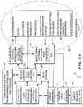
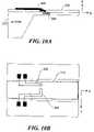
- FIG. 1Ais a functional block diagram illustrating an image acquisition system including supporting components for processing signals from, and controlling various components that are placed inside a patient's body;
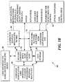
- FIG. 1Bis a functional block diagram illustrating a display system including supporting components.
- FIGS. 2A , 2 B, and 2 Crespectively illustrate a top plan view, a side elevational cross-sectional view taken along section line 2 B- 2 B in FIG. 2A , and an end view taken along section line 2 C- 2 C in FIG. 2A , of a first prototype embodiment of a thin film, rectilinear illuminator;
- FIG. 2Dillustrates an end elevational view of a second prototype embodiment that includes a pair of thin film parallel cantilevers for illumination of an ROI;
- FIG. 3is an isometric view of an integrated image acquisition scanner system
- FIG. 4is an isometric view of an integrated display scanner system
- FIG. 5is an isometric view of an integrated collecting scanner system
- FIG. 6Ais an isometric view of a hybrid emitting scanner system
- FIG. 6Bis an isometric view of a cantilevered laser diode system
- FIG. 6Cis an isometric view of a cantilevered fiber waveguide system
- FIG. 7Ais an isometric view of the free end of the cantilever waveguide formed into a gradient index lens
- FIG. 7Bis an isometric view of the cantilever waveguide with a micro refractive lens
- FIG. 7Cis an isometric view of the cantilever waveguide with a Fresnel lens
- FIG. 7Dis an isometric view of the cantilever waveguide with Fresnel lens microfabricated on to an upper surface of the cantilever waveguide;
- FIG. 8Ais a side sectional view of a scanner showing a vertical actuator that utilizes electrostatic force
- FIG. 8Bis a plan view of a scanner showing a horizontal actuator that utilizes electrostatic force
- FIG. 9Ais a side sectional view of the scanner showing a layered configuration of a vertical actuator that utilizes the piezoelectric effect
- FIG. 9Bis a plan view of the scanner illustrating a configuration of traces for energizing conductive layers for the vertical actuator that utilizes the piezoelectric effect;
- FIG. 10Ais a side sectional view of a scanner with a piezoresistive transducer integrated into the cantilever;
- FIG. 10Bis a plan view of the scanner with two piezoresistive transducers integrated into the cantilever for measuring vertical and horizontal motion of the cantilever.
- the present inventioncan also be embodied in a non-medical image acquisition device, a wearable display, a biological, chemical or mechanical sensor, or any other miniature high resolution, far-field device.
- the inventioncan be used to illuminate specific patterns for microlithography, micro-inspection, and micro-illumination.
- the inventioncan further be embodied in a bar code reader, a range finder, or a device for combining simultaneous sensing and delivery functions.
- the present inventioncan be used to integrate both imaging and non-imaging functionality, such as diagnosis, monitoring, and therapy of an internal ROI, instead of requiring separate instruments for imaging and for rendering therapy or other functions to a site.
- an integrated endoscopecan provide ultra violet therapy and monitoring.
- many optical diagnostic and therapeutic techniquesrely on high quality illumination at elevated intensities, which is inherent in optical scanning and cannot be achieved with diffuse illumination. A scanned beam of intense optical energy is more effective at overcoming the signal-to-noise limitations of photon detectors used in conventional diagnostic imaging systems.
- fluorescent dye moleculesare used as tracers for specific cells or structures, the signal conversion rates from illumination to fluorescence are very low and often buried in noise.
- PDTphotodynamic therapy
- the optical excitation of PDT labels on cancerous cellscreates free radicals that kill nearby cells.
- Doses of intense optical illuminationare applied to overcome the natural buffering mechanisms within the body, to attain effective concentrations of free radicals.
- Laser therapies that rely on optical heating, cutting, and cauterization of tissuesrequire the highest optical intensities that can be delivered and cannot be used effectively with diffuse illumination. Directed, focused beams of light on tissue for precise exposure times are necessary for reducing surrounding tissue damage which is provided in a controlled optical scan system.
- high quality illuminationcan include a high degree of optical monochromaticity, coherence, polarization, high modulation frequency, high pulse repetition rates, and short pulse duration.
- FIG. 1AAn example system for providing imaging and non-imaging functionality through an endoscope is shown in FIG. 1A . More specifically, FIG. 1A illustrates a system 50 that shows how the signals produced by components of the integrated image acquisition device that is placed inside a patient's body are processed with external instrumentation and how signals used for controlling the system are input to the components that are inside the patient's body.
- system 50is thus divided into the components that remain external to the patient's body, and those which are used internally (i.e., the components within a dash line 52 ).
- a block 54lists functional components of the integrated image acquisition device and/or other components disposed at the distal end of the endoscope.
- these componentspreferably include one or more light sources, optical components, actuators, cantilever scanners, waveguides, lenses, photon detectors, motion detectors for motion control of the scanner(s) and/or control of the distal end of the endoscope, photon detectors for imaging the ROI.
- additional photon detectorsmay be included for diagnostic purposes and for therapy and monitoring purposes.
- one or more local controllersmay be integrated for localized processing of control signals and detected signals. It should be noted that in regard to system 50 , only the functional components actually required for a specific application may be included. Also, the additional functions besides imaging can include diagnostic, or therapy, or a combination of these functions.
- additional or alternate illumination sources, modulators, filters, and detectorsmay be provided as shown in a block 56 .
- external light source systems for producing red, green, blue (RGB), ultraviolet (UV), Infrared (IR), and/or high intensity lightmay include a delivery component to convey light to the distal end of the endoscope.
- all or portions of the additional or alternate illumination sourcesmay be partially, or completely inside the patient's body.
- additional light emitting diodesmay be integrated with the components of block 54 at the distal end of the endoscope.
- modulators, filters, and detectorsare also optionally coupled to the electromechanical scan actuator(s) inside the patient's body and to the scanner control actuators. Scanner motion detectors are used for controlling the scanning and produce a signal that may be fed back to the scanner actuators, illumination source, and modulators to implement scanning control.
- image signal filtering, buffering, scan conversion, amplification, and other processing functionsare implemented using the electronic signals produced by the imaging photon detectors and for the other photon detectors employed for diagnosis/therapy, and monitoring purposes. As illustrated, some or all of these functions may alternatively be implemented with integrated circuitry that is near the distal end of the endoscope inside the patient's body.
- Blocks 56 and 60are interconnected bi-directionally to convey signals that facilitate the functions performed by each respective block.
- each of these blocksis bi-directionally coupled in communication with a block 62 in which analog-to-digital (A/D) and digital-to-analog (D/A) converters are provided for processing signals that are supplied to a computer workstation user interface employed for image acquisition, processing, for executing related programs, and for other functions. Control signals from the computer workstation are fed back to block 62 and converted into analog signals, where appropriate, for controlling or actuating each of the functions provided in blocks 56 and 60 .
- the A/D converters and D/A converters within block 62are also coupled bi-directionally to a block 64 in which data storage is provided, and to a block 66 .
- Block 66represents a user interface for maneuvering, positioning, and stabilizing the end of the scanning optical waveguide within a patient's body.
- the data storageis used for storing the image data produced by the detectors within a patient's body, and for storing other data related to the imaging and functions implemented by the scanning optical waveguide.
- Block 64is also coupled bi-directionally to the computer workstation and to interactive display monitor(s) in a block 70 .
- Block 70receives an input from block 60 , enabling images of the ROI to be displayed interactively.
- one or more passive video display monitorsmay be included within the system, as indicated in a block 72 .
- Other types of display devicesfor example, a head-mounted display (HMD) system, can also be provided, enabling medical personnel to view an ROI as a pseudo-stereo image.
- the HMD systemcan include a display embodiment of the invention to display the image acquired from within the patient's body.
- the display embodimentis effectively an inverse of the image acquisition system.
- System 80shows how signals are process by various components for display on a target surface in a ROI.
- a block 84lists the functional components of an integrated display scanner. Similar to the image acquisition system discussed above, the components of the integrated display scanner preferably include one or more light sources, actuators, cantilever scanners, waveguides, lenses, local controllers, and tip displacement sensors. In addition, the integrated display scanner preferably further includes one or more light modulators and filters, although these components can be non-integrated, as shown in block 86 . Photon detectors can be included for monitoring the displayed image and/or measuring motion of the cantilever scanner(s), but photon detectors are not required for a display device.
- Blocks 86 and 90are interconnected bi-directionally to convey signals that facilitate the functions performed by each respective block.
- each of these blocksis bi-directionally coupled in communication with a block 92 in which analog-to-digital (A/D) and digital-to-analog (D/A) converters are provided for processing signals that are supplied to or by a computer workstation user interface employed for image display, for processing, for executing related programs, and for other functions.
- A/Danalog-to-digital
- D/Adigital-to-analog
- Control signals from the computer workstationcan be fed back to block 92 and converted into analog signals, where appropriate, for controlling or actuating each of the functions provided in blocks 86 , 90 and 84 .
- the A/D converters and D/A converters within block 92are also coupled bi-directionally to a block 94 in which data storage is provided, and to a block 96 .
- Block 96represents a user interface for maneuvering, positioning, and stabilizing the end of the scanning optical waveguide for display.
- Block 94is also coupled bi-directionally to the computer workstation, and the data storage is used for storing the image data, and for storing other data related to the display and functions implemented by the scanning optical waveguide.
- one or more passive video display monitorsmay be included within the system (not shown) for test purposes. Further detail is discussed below with regard to FIG. 4 .
- FIGS. 2A , 2 B, and 2 Cillustrate an early prototype of a thin film optical system 140 , in which this approach was shown to be effective.
- a further alternative 140 ′ illustrated in FIG. 2Dincludes parallel cantilevered thin film optical waveguides for scanning and detectors.
- electrostatic actuators 156act on a thin film optical waveguide 150 that is supported on a raised ledge 148 .
- the thin film optical waveguideis only approximately 0.003 mm in diameter.
- a distal portion 152 of the thin film optical waveguideis caused to scan in the two orthogonal directions indicated by the curved arrows in FIGS. 2A and 2B .
- the scanning motioncan be one-dimensional (i.e., along a single axis), or as shown, in two dimensions (e.g., along a raster pattern or a spiral pattern).
- the thin film optical devicecan be mounted on a rod 143 , which is then manually or mechanically rotated or vibrated to change the orientation or displace the single axis scan.
- a lens 154that is preferably mounted to a silicon substrate 146 (or other substrate material).
- external actuatorscan be used instead of the electrostatic actuators, in which case, an optical fiber 144 and lens 154 would be supported by silicon substrate 146 , which would be caused to vibrate by the external actuators, causing the cantilevered thin film optical waveguide to resonantly scan.
- Optical fiber 144is preferably affixed to silicon substrate 146 within a centering V notch 160 to ensure that it is aligned with thin film optical waveguide 150 . Since the optical fiber is approximately 0.1 mm in diameter, care must be taken to provide accurate alignment between the ends of the optical fiber and the thin film optical waveguide.
- FIGS. 2A and 2Bshow the embodiment using butt-end coupling between optical fiber 144 and a thin film optical waveguide 150 .
- V notch 160precisely establishes a disposition of the optical fiber relative to the thin film optical waveguide.
- An index-matching gel 145 or fluidcan be used to couple light from optical fiber 144 to thin film optical waveguide 150 .
- the tip of the optical fibercan be etched to form a taper. Further, the tip length and surface can be adjusted by CO 2 laser machining before affixation. Other embodiments described below further alleviate alignment problems.
- RGB detectors 162 r , 162 g , and 162 brespectively. These detectors respond to the light of the corresponding color, producing a signal that is conveyed proximally to the external components, as discussed above.
- FIG. 2Dseparate image and diagnostic/therapeutic thin film optical waveguides are spaced apart and scanned in parallel; this embodiment uses a diagnostic “DIAG” detector 162 d.
- FIG. 3is an isometric view of an integrated emitting scanner system 200 .
- Emitting scanner system 200can perform image acquisition and/or display by directing emitted light with a flexible cantilever.
- emitting scanner system 200will be described primarily with regard to image acquisition.
- an imageis acquired by scanning a waveguide and capturing the image with one or more stationary light detectors.
- the waveguidewill be driven to resonance, but motion is not restricted to operating at resonance.
- an image planeis generated by scanning light from the single resonant waveguide.
- this approachis beneficial, since it is capable of providing a wide optical field of view (FOV) in a relatively small movement volume.
- FOVoptical field of view
- This approachalso provides high image resolution, because an illuminated spot size determines pixel resolution rather than a sample area size. Thus, the detector size and number do not affect the image resolution.
- Image resolutioncan also be altered to create a zoom mode by changing scanning amplitudes and/or the sampling rate of the light detector.
- Emitting scanner system 200creates an illuminated spot on a target 190 by scanning light from a light source 202 .
- Light source 202preferably comprises a semiconductor device such as a light-emitting diode (LED) or a laser diode, so that the light source can be fabricated along with a scanner 210 using conventional micro-fabrication techniques.
- an external light sourcecan alternatively be coupled to scanner 210 with an optical fiber or other waveguide.
- an emitter 204when voltage is applied to light source 202 from a power lead 203 , an emitter 204 generates light.
- Light source 202is preferably end-butted to cantilever 212 , which acts as a waveguide to direct emitted light from a fixed end 214 to a free end 216 .
- Fixed end 214is attached to a substrate 220 such as n-type silicon.
- substrate 220is etched to create a channel 222 into which free end 216 can deflect.
- Free end 216may include a lens 218 to collimate or focus the light onto target 190 .
- Free end 216is preferably driven into resonance in one or more orthogonal directions to create an illuminated spot on target 190 .
- a vertical actuator 230can deflect cantilever 212 in a vertical direction relative to a primary plane of substrate 220 .
- a horizontal actuatorcan be implemented with deflection electrodes 234 a - 234 d to deflect cantilever 212 in a horizontal direction relative to the primary plane of substrate 220 .
- free end 216can illuminate target 190 in a raster scan pattern, a spiral pattern, or other pattern.
- the free endcan be deflected into a two-dimensional circular motion or into a two-dimensional rocking motion using a single actuator.
- the illuminationcan be used for acquiring an image, displaying an image, performing a therapy, or performing another function.
- Position sensor array 236detects the vertical and horizontal position of free end 216 as a function of a conductive layer 235 that is integrated onto cantilever 212 . This or other position sensor implementations enable long term control of scanning stability.
- FIG. 4is an isometric view of an integrated display scanner system 201 for generating an image on a display surface 191 .
- An RGB light source 205is preferably used to generate the display light.
- a light delivery component of an external light sourcecan be used.
- RGB light source 205is preferably implemented with different colored LEDs 209 a - 209 c , which preferably include different concentrations of dopant to create different wavelengths of light.
- the RGB lightsare coupled via a 3 ⁇ 1 coupler 207 to fixed end 214 of cantilever 212 , which acts as a waveguide to scan the light for display.
- a white light source with a built-in tunable color filtercan be used.
- the built-in tunable color filtercan be in an interferometer, grating, or prism configuration to provide the preferred color light to the scanner.
- the tunable filteris controlled by a light modulating circuit (not shown) based on the information provided from image processing software.
- a more definite color lightis possible.
- Using a tunable filteralso eliminates the need for three color input.
- the lightcan alternatively delivered via a fiber that is coupled to the scanning cantilever waveguide.
- the image to be displayedis converter to binary code using image processing software.
- Output codesare then downloading to a microprocessor (not shown) coupled to the light modulating circuit (not shown).
- the lightsare strobed at a frequency based on the information provided by the microprocessor.
- An integrated lens or an external lens 218is place near the tip to provide the magnification needed for the image display.
- mechanical scanningis provided by vertical actuator 230 and horizontal actuators 234 a - 234 d .
- the position of free end 216is monitored by the same type of position sensors as used for the image acquisition system.
- the information provided by the position sensorsis used by an actuator control circuit to maneuver, position and/or stabilize free end 216 for creating the displayed image.
- FIG. 5is an isometric view of an integrated collecting scanner system 240 .
- cantilever 212is used for image capture. This approach is less efficient than the emitting scanner system described above, because the resolution is limited by the numerical aperture of the image detection system used (e.g., the lens, waveguide, and detector). However, this approach is useful for specialized imaging and optical sensing where full illumination of the target and the image detector is required.
- lightis generated by an one or more laser diodes 208 with emitter layer 204 butt-end coupled to, and aligned with one or more stationary semiconductor waveguides such as stationary waveguides 242 a and 242 b .
- the lightis directed along the stationary waveguides and onto target 190 .
- the back scattered lightis received with cantilever 212 , which is preferably driven in a rectilinear scanning motion by vertical actuator 230 and the horizontal actuator implemented with deflection electrodes 234 a - 234 d .
- the back scattered lightmay pass through a lens 244 such as a diffractive lens.
- the photodiodecan be integrated into the free end of the cantilever.
- FIG. 6Ais an isometric view of a hybrid emitting scanner system 250 that includes a simplified emitting scanner 252 for scanning light onto the target, and a separate simplified collecting system 254 to receive and detect the backscattered light.
- Simplified emitting scanner 252does not need the integrated photon detectors.
- a flexible optical fiber 256can be positioned near the illuminated area of target 190 to receive the backscattered light. Flexible optical fiber 256 directs the received light through a coupler 258 to an optional semiconductor waveguide 260 , which directs the light to one or more photon detectors 262 .
- the primary advantage of a hybrid approachis that various substrate materials can by selected to optimize the performance of each component.
- FIG. 6Bis an isometric view of a cantilevered laser diode system 270 .
- a laser diode 272is attached to free end 216 of cantilever 212 .
- cantilever 212provides electrical connections to laser diode 272 , rather than transmitting light from a laser diode optically coupled to cantilever 212 .
- all of cantilever 212can be fabricated as a laser diode.
- FIG. 6Cis an isometric view of a cantilevered fiber waveguide system 280 .
- An optical fiber 282that can be etched to reduce mass, is coupled to cantilever 212 so that light is emitted from free end 216 .
- a parallel array of cantileverscould be fabricated adjacent to each other and actuated in one dimension, thus creating a light scan over an area.
- This devicewould not require the relatively fast scan rates and large amplitudes of a single scanning waveguide.
- the functional componentssuch as the laser diode light source, the waveguide, the photodiodes, the coupler, the position sensors and actuators can be integrated on separate substrates, each consisting of stacked functional modules.
- the light sourcemight use a different substrate from that supporting the cantilever.
- GaAscan be used for the laser diode substrate for its ideal optical emission spectrum and output power efficiency. Further details regarding embodiments of the components comprising collecting scanner systems and emitting scanner systems are described below.
- the cantilevercomprises a two-layer composite of silicon oxide (SiO 2 ) and silicon.
- the SiO 2is used as an optical core through which the light travels.
- SiO 2has less-than-desirable mechanical properties.
- a thin SiO 2 layer of approximately 2.2 micrometers ( ⁇ m)is thermally grown on a layer of single crystal silicon that is approximately 30 ⁇ m thick. The silicon layer gives the composite cantilever increased mechanical stiffness and durability.
- a low index buffer layerto optically isolate the silicon layer from the SiO 2 layer, because silicon has a high index of refraction and is absorbing in the visible band.
- the buffer layercan be omitted without excessive optical power loss.
- a film of silicon nitride (Si x N y ), or other compoundcan be used as the waveguide.
- a thick (Si x N y ) filme.g., >1 ⁇ m
- a preferred cantilever embodimentincludes a thicker cantilever waveguide comprised of a mechanically durable material that still provides good optical transmission.
- SU-8 photoresistoriginally developed by IBMTM (see U.S. Pat. No. 4,882,245).
- SU-8offers beneficial imaging capabilities such as vertical sidewall profiles and dimensional control over an entire structure height.
- high functionalityresults in minimal swelling.
- Processing advantagesinclude a highly cross-linked structure, which results in chemical resistance and high thermal characteristics and processing to greater than 200° C.
- SU-8offers good adhesion to most surfaces as well as improved wetting on silicon glass, metals, and other low surface energy substrates. With its exposure near ultraviolet (UV) wavelengths (350-400 nm), SU-8 is a cost effective alternative to expensive X-ray processing.
- UVnear ultraviolet
- cantilever 212preferably comprises an SU-8 cantilever waveguide that is approximately 85 ⁇ m thick at the fixed end and tapered to fit within a smaller diameter toward the free end.
- Cantilever 212is also approximately 125 ⁇ m wide, and approximately 0.5 mm to 1.0 mm long from fixed end 214 to free end 216 .
- An overall larger coupling area at the fixed endmakes it much easier to couple a light source to the cantilever waveguide, and increases the amount of light coupled into the cantilever waveguide.
- a tapered waveguide coupler(not shown) can be fabricated between the light source and the cantilever waveguide (or stationary waveguides).
- the SU-8 epoxy resinalso makes the cantilever waveguide more durable.
- the modulus of elasticity of SU-8(4.02 GPa) is less than the SiO 2 /Si composite beam (silicon 125 GPa and silicon oxide 57 GPa), the increased thickness of the SU-8 cantilever waveguide results in resonant frequencies of approximately 20 kHz, which is typical of sVGA video rates.
- Cantilever 212is preferably formed by first spin coating the SU-8 photoresist onto the silicon substrate.
- the SU-8is exposed with a mask to define the shape of the cantilever.
- the unexposed SU-8is removed with a developing solution.
- a deep reactive ion etching (REI) processthen etches the silicon substrate down to near the fixed end to release the SU-8 cantilever.
- REIdeep reactive ion etching
- Cantilever 212can also be tapered with fixed end 214 being wider than free end 216 . Tapering increases angular tip deflection, which provides a larger FOV. However, increased tip deflection may have to be balanced against the overall device size that is desired for a given application. Tapering can also be used to reduce the effective point source size of light emitted from the cantilever.
- FIGS. 7A-7Dillustrate some of the possible lens implementations.
- FIG. 7Ais an isometric view of the free end of the cantilever waveguide formed into a gradient index lens 290 .
- FIG. 7Bis an isometric view of the cantilever waveguide with a micro refractive lens 292 placed near the free end to focus the light onto the target.
- Micro refractive lens 292can be fabricated from fused silica or SiO or any other waveguide material using standard solid-state process. Micromolding techniques using silicone rubber and positive photoresist can also be employed.
- FIG. 7Cis an isometric view of the cantilever waveguide with a Fresnel lens 294 placed at the free end. The number of bands and the separation between each band can be adjust piezoelectrically to control the central maximum of the light beam and its focal length.
- FIG. 7Dis an isometric view of the cantilever waveguide with Fresnel lens 294 microfabricated on to an upper surface of the cantilever waveguide.
- a variety of actuatorscan be implemented to drive the cantilever.
- One embodimentutilizes electrostatic force.
- An electrostatic actuatoris advantageous for a number of reasons, including:
- FIG. 8Ais a sectional view of a scanner showing a vertical actuator that utilizes electrostatic force.
- an electrode pad 302is deposited onto substrate 220 under cantilever 212 .
- Electrode pad 302is preferably fabricated from an electrically conductive thin film such as Al, Ag, Au, Pt or Cu.
- an electrostatic forceis generated between cantilever 212 and substrate 220 .
- the electrode gap distanceis limited to a few hundred microns.
- a sinusoidal voltageis applied to electrode pad 306 .
- a bumper 304can be fabricated under the cantilever to prevent the displaced cantilever from touching position sensor 236 .
- the cantileveralso acts as an isolator between electrode pad 306 and conductive layer 235 . This prevents conductive layer 235 from sticking to substrate 220 .
- FIG. 8Bis a plan view of a scanner showing a horizontal actuator that utilizes electrostatic force.
- Horizontal deflection electrodes 234 a - 234 dcomprise the horizontal actuator.
- Voltageis selectively applied to a pair of electrodes on one side of cantilever 212 (e.g., horizontal deflection electrodes 234 a and 234 b ). The voltage creates an electrostatic force that draws cantilever 212 toward the energized pair of electrodes.
- a sinusoidal voltageis applied to one pair of horizontal deflection electrodes, while phase shifted sinusoidal voltage is applied to the opposite pair of horizontal deflection electrodes.
- the two sinusoidsare 180 degrees out of phase with each other.
- One or more bumpers 310can be used to limit the motion of free end 216 .
- an array of position sensors 236can be used to detect the position of free end 216 to maintain control of cantilever 212 .
- the electrostatic actuatoris not bandwidth limited by the scanning frequency, this technique can provide a higher scan rate than required by most standard video displays such as 31.5 kHz for VGA and 37.5-40 kHz for SVGA. Note, however, that for bidirectional scanning, the frequency of the cantilever need only be half of these stated values.
- a macro scale raster scanning devicecan be used as an identification (ID) scanner or a bar code scanner.
- IDidentification
- the waveguidemust be driven with a large base excitation to attain a large FOV. By controlling the excitation frequency, phase and amplitude, a steady in-and-out swirling scanning pattern can be achieved from free end 216 .
- a circular scan patterncan be excited by applying excitation in horizontal and vertical directions ninety degrees out of phase.
- the circular pattern with varying radiican be controlled by the amplitude of the excitation.
- a rotating rectilinear scan patterncan be excited by applying electric potentials to two electrodes placed slightly at an angle to each other rather than orthogonal to each other. To generate the rotation on the rectilinear motion, a larger voltage must be applied to the electrodes for one direction (e.g., angled electrodes) than the voltage applied to the electrodes for the other direction (e.g., vertical electrodes). The result is a line sweep rocking back and forth between 0 and 180 degrees.
- the relationship between deflection of free end 216 and the applied voltagecan be nonlinear.
- an electrostatic comb drivecan be used as the actuator such as that described by W. C. Tang et al. ( IEEE Sensors and Actuator Workshop . A21, 23 (1990)).
- the capacitanceis varied through changing area, not the gap. Since capacitance is linearly related to area, the displacement will vary as the square of the applied voltage.
- harnessing the nonlinearity of cantilever deflectionwould be advantageous in that it would then be possible for a single actuator to generate two-dimensional (2D) motion of free end 216 .
- a piezoelectric effectis used for vertical actuator 230 shown in FIGS. 3-6C .
- the advantages of using a piezoelectric driverinclude:
- the disadvantage of using piezoelectric thin film for an actuatoris that the actuator requires a high voltage for displacement in the micron regime.
- the problemcan be partially alleviated by implementing a bimorph configuration.
- the crystalline structureproduces a voltage proportional to the pressure.
- an electric fieldis applied, the structure changes shape producing dimensional changes in the material.
- dijis a charge sensitivity coefficient
- xis the spacing between the two conducting plates of area A
- ⁇ o and ⁇ rare air and material dielectric constants, respectively.
- the electro-mechanical materials preferably used for a microactuatorare ZnO, lead zirconate titanate (PZT) and polyvinylidene fluoride (PVDF).
- PVDFpolyvinylidene fluoride
- PVDFis preferably deposited as spin cast film from dilute solution in which PVDF powder has been dissolved.
- FIGS. 9A and 9Bshow an example of a piezoelectric thin film actuator for the scanning system.
- FIG. 9Ais a side sectional view of the scanner showing a layered configuration of a vertical actuator that utilizes the piezoelectric effect.
- Vertical actuator 230includes a conductive layer 306 comprising Cr/Au, Al, or other suitable conductive material. The same material is preferably used for cantilever conductive layer 235 that is deposited on the surface of cantilever 212 . Between these conductive layers is an insulating layer 308 comprising a piezoelectric film such as ZnO, PZT, PVDF, or other suitable material.
- FIG. 9Ais a side sectional view of the scanner showing a layered configuration of a vertical actuator that utilizes the piezoelectric effect.
- Vertical actuator 230includes a conductive layer 306 comprising Cr/Au, Al, or other suitable conductive material. The same material is preferably used for cantilever conductive layer 235 that is deposited on the surface
- FIG. 9Bis a plan view of the scanner illustrating a configuration of traces for energizing the conductive layers.
- a trace 310is used to provide sinusoidal voltage to conductive layer 306 .
- Another trace 312is used to connect conductive layer 235 as a return reference.
- a position sensorthat can be integrated into a small area such as less than 3 mm.
- light losscan be measured from waveguide bending. All waveguides lose light from their cores to the outside environment.
- a scanning waveguidealso loses light to the environment in proportion to the deflection of the waveguide. This proportional loss is called bending loss.
- a devicesuch as a photodetector or photodetector array that detects the quantity of light lost from the waveguide in proportion to the waveguide's motion can therefore measure the free end position of the waveguide.
- NSMnear field scanning microscopes
- a variety of position sensorscan also be implemented to detect the position or other motion characteristic of the cantilever.
- the position sensor embodiment shown in FIGS. 3 through 6Cuses a capacitive effect.
- the capacitive effectis one of the simplest precision sensing mechanisms for measuring displacement.
- a capacitive sensordetects changes in capacitance when the distance between two charged plates increases or decreases.
- capacitive sensor structuresare relatively simple to fabricate.
- a capacitive displacement sensorincludes one moving plate and one fixed plate. As shown in FIG. 3 , the moving plate corresponds to conductive layer 235 on top of cantilever 212 .
- the fixed platecorresponds to position sensor array 236 , which is located on substrate 220 in channel 222 under free end 216 of cantilever 212 .
- An array of electrodesis used to enable position detection in both vertical and horizontal directions relative to a primary plane of substrate 220 .
- Displacement in the horizontal directionis detected based on the area of each position sensor electrode that is covered by conductive layer 235 while cantilever 212 moves horizontally.
- Vertical displacementis detected based on the vertical distance between conductive layer 235 and position sensor array 236 .
- the changing capacitancecan be measured using a number of well-known circuit techniques, such as:
- a piezoelectric position sensorincludes a piezoelectric thin film deposited on both sides of the cantilever. Displacement of the cantilever is determined by the measuring the strain-induced electric field on the piezoelectric thin film.
- the configuration of a piezoelectric position sensoris the same as the piezoelectric actuator shown in FIGS. 9A and 9B . However, the sensor area can be extended to cover the entire length of the cantilever, thereby increasing the deflection sensing capability.
- a piezoelectric displacement sensorhas some unique advantages.
- PZTIn addition to large piezoelectric coupling, PZT has a large pyroelectric response and a large spontaneous polarization, which makes PZT a good candidate material for infrared (IR) detectors (See, D. Polla, Ph.D. Dissertation, Univ. of Cal., Berkeley, (1985)). If an IR scanning scope (for low light image acquisition) is needed, the same material can be used for light detection. Another advantage of this approach is that the material can also be used as the actuator.
- IRinfrared
- a piezoeresistance position sensorcomprises a semiconductor strain gauge such as taught by J. J. Wortman et al., IEEE Elect. Dev. 16, 855 (1969); B. Puers et al., IEEE Elect. Dev. 35, 764 (1988) and S. R. Manalis, Appl. Phys. Lett. 69, 3944 (1996)).
- the position sensorcomprises electrically conducting, strain-sensitive regions that are fabricated by diffusing impurities, such as a boron dopant, into a highly resistive, single-crystal cantilever.
- a p-type layer of boroncan be diffused into an n-type silicon layer on the cantilever.
- the diffusion processpreferably comprises open-tube boron diffusion from boron nitride, or boron ion plantation.
- FIGS. 10A and 10BA bi-axial displacement sensor is illustrated in FIGS. 10A and 10B . More specifically, FIG. 10A is a side sectional view of a scanner with a piezoresistive transducer integrated into the cantilever.
- a vertical piezoresistive transducer 324comprises a p-type diffused resistor that is oriented along the primary longitudinal axis of cantilever 212 .
- Vertical piezoresistive transducer 324detects vertical deflection (e.g., in a Z direction) of cantilever 212 relative to a primary plane of substrate 220 .
- a horizontal piezoresistive transducer 326also comprises a p-type diffused resistor, but is oriented along a secondary transverse axis of cantilever 212 .
- Horizontal piezoresistive transducer 326detects horizontal deflection (e.g., in a Y direction) of cantilever 212 relative to the primary plane of substrate 220 .
- FIG. 10Bis a plan view of the scanner with two piezoresistive transducers integrated into the cantilever.
- a p-type (e.g., boron doped) piezoresistor 320is diffused into cantilever 212 .
- piezoresistor 320is diffused into an n-type substrate such as silicon (e.g., with 100 surface orientation).
- a silicon cantilevercan be used, or a silicon layer can be fabricated under a waveguide layer such as a layer of SU-8.
- a windowis provided through the waveguide layer so that a conductive contact 322 can be connected to piezoresistor 320 .
- a position sensorthat can be integrated into a small area such as less than 3 mm.
- light losscan be measured from waveguide bending. All waveguides lose light from their cores to the outside environment.
- a scanning waveguidealso loses light to the environment in proportion to deflection of the waveguide. This proportional loss is called bending loss.
- a devicesuch as a photodetector or photodetector array that detects the quantity of light lost from the waveguide in proportion to the waveguide's motion can therefore measure the free end position of the waveguide.
- NSMnear field scanning microscopes
- a ferromagnetic materialcan be deposited on the scanning waveguide, so that the free end position can be tracked with inductive coils.
- a magnetic sensorcan detect a change in magnetic field.
- an integrated, dual axis interferometercan be used to detect the vertical and horizontal position of the free end of the waveguide.
- a piezoresistive sensorcan also be used in the cantilever to detect position. If space is available, a quadrant fiber bundle can be used to detect light provided from the free end of the waveguide. Additionally, the actuator itself can be used to detect position.
- photon detectors 224 a and 224 bdetect light backscattered from the target in the ROI.
- photodiode 246 shown in FIG. 5detects light directed back through the cantilever waveguide.
- these light detectorsare of the same wavelength spectrum or the same red, green, blue (RGB) spectrums.
- the light detectorsare also preferably constructed from a silicon substrate, which can be the material used in the waveguide, actuator, coupler and displacement sensor.
- a silicon photodiodeis known for light wave detection in the wavelength ranges of 0.4 ⁇ m to 1 ⁇ m due to silicon's high responsiveness near that wavelength spectrum.
- Siliconalso has the virtues of high quantum efficiency, good linearity of response, large bandwidth, simple bias option, and relatively low cost.
- a common type of optical detectoris a depletion-layer photodiode.
- the depletion-layer photodiodeis essentially a reverse-biased semiconductor diode, wherein reverse current is modulated by electron-hole pairs produced in or near the depletion layer by the absorption of photons.
- the simplest depletion layer photodiodeis a p-n junction diode.
- the diodecan be hybridized with a waveguide and a fiber detector to optimize the intensity absorption.
- the backscattered lightis first captured by single optical fiber 256 or a fiber bundle detector. Then the light is inserted into waveguide 260 through a grating or mechanical coupler 258 such as a V-groove and/or silicon nitride clips. The light is directed to the other end of the waveguide where the light is received by photon detector 262 , which is preferably a silicon photodiode.
- the diodecan be formed by boron diffusion to a n-type silicon substrate in a manner similar to that described above with regard to the piezoresistor and/or as described by D. Ostrowsky et al., App. Phys. Lett. 22 (1973).
- a thick layer (several micrometers) of waveguide material made of either SiO 2 or silicon nitridecan also be grown and used as a diffusion mask and later left as the waveguide.
- Metal electrodesare added to complete the structure.
- the benefit of having the fiber detectoris that it allows the photodetector to be at the proximal end of the probe without actually having the photodiode placed near the probe. In this hybrid design, the photodiode is less affected by noise and environmental factors.
- the fibercan also be coated with metal and bent to a desired viewpoint. In addition, a separate support can be used to stabilize the tip of the fiber during high resolution imaging.
- the small detecting area on the diode(approximately few tens of microns in diameter) provides giga hertz (GHz) range bandwidth.
- GHzgiga hertz
- these silicon-based photodiodescan offer sufficient bandwidth in the visible spectrum (e.g., the photodetector bandwidths must exceed 12.5 MHz for VGA and 19.8 MHz for SVGA video standard).
- an intrinsic region of high resistivitycan be added to the p-n junction to form a so-called PIN structure.
- an avalanche photodetector (APD) structurecan be implemented, such as that described by P. P. Webb, IEEE solid state sensors symposium. 96 (1970).
- APDavalanche photodetector
- a basic p-n structureis operated under a very high reverse bias.
- the current multiplication for an avalanche diodecan be as high as 4 orders of magnitude (based on commercially available photovoltaic photodiode and APD from UDT Sensor LTD).
- modular componentscan be constructed separately, each with an optimal substrate.
- the modular componentscan then be bonded together use anodic, adhesive, or other bonding methods. Accordingly, it is not intended that the scope of the invention in any way be limited by the above description, but instead be determined entirely by reference to the claims that follow.
Landscapes
- Health & Medical Sciences (AREA)
- Life Sciences & Earth Sciences (AREA)
- Physics & Mathematics (AREA)
- Surgery (AREA)
- Optics & Photonics (AREA)
- Medical Informatics (AREA)
- Public Health (AREA)
- Veterinary Medicine (AREA)
- Pathology (AREA)
- Engineering & Computer Science (AREA)
- Biomedical Technology (AREA)
- Heart & Thoracic Surgery (AREA)
- Biophysics (AREA)
- Molecular Biology (AREA)
- Animal Behavior & Ethology (AREA)
- General Health & Medical Sciences (AREA)
- Nuclear Medicine, Radiotherapy & Molecular Imaging (AREA)
- Radiology & Medical Imaging (AREA)
- General Physics & Mathematics (AREA)
- Micromachines (AREA)
- Mechanical Optical Scanning Systems (AREA)
- Radiation-Therapy Devices (AREA)
- Laser Surgery Devices (AREA)
- Mechanical Light Control Or Optical Switches (AREA)
- Instruments For Viewing The Inside Of Hollow Bodies (AREA)
- Optical Couplings Of Light Guides (AREA)
- Microscoopes, Condenser (AREA)
Abstract
Description
- it involves a very simple mechanism comprising a condenser of two conducting surfaces;
- it can be used as a driver as well as a position sensor for the cantilever; and
- the fabrication techniques used in device manufacture are compatible with mass production using the existing micro-fabrication technology, providing low device costs and high production yields.
- the cantilever does not stick to the electrodes when it is driving too close to the substrate;
- the actuation mechanism would be highly resistive to environmental effect (e.g. humidity, temperature); and
- thin film deposition is compatible with VLSI processes (e.g. deposition methods and etching).
ΔV=dijxΔF/∈o∈rA
- charge-sensitive amplifier;
- impedance measurements in a bridge configuration (See, Bao et al.,Proc. Annu. Conf. Eng. Med. Biol.22, 119 (1980));
- RC oscillators using a CMOS 555 timer. In effect this process converts the unknown capacitance into a time-constant by determining capacitance in an oscillator and measuring the frequency. (M. R. Nueman et al.,IEEE Frontier Eng. Comp. Health Care Conf.436 (1984)); and
- direct charge coupling such as using the moving plate as the gate of a field-effect transistor (W. Kuhnel et al.,Sensors and ActuatorsA32, 560 (1992)).
ΔR/R=πlTl+πtTt
where πland πtare longitudinal and transverse piezoresistance coefficients, and Tland Ttare stresses parallel and perpendicular to the direction of current in the layer.
Claims (54)
Priority Applications (7)
| Application Number | Priority Date | Filing Date | Title |
|---|---|---|---|
| US10/655,482US7555333B2 (en) | 2000-06-19 | 2003-09-04 | Integrated optical scanning image acquisition and display |
| JP2006525541AJP2007503938A (en) | 2003-09-04 | 2004-09-03 | Integrated optical scanning image acquisition and display |
| EP04788635AEP1671176A4 (en) | 2003-09-04 | 2004-09-03 | INTEGRATED ACQUISITION AND DISPLAY OF IMAGES BY OPTICAL SCANNING |
| CA002534477ACA2534477A1 (en) | 2003-09-04 | 2004-09-03 | Integrated optical scanning image acquisiting and display |
| AU2004269796AAU2004269796A1 (en) | 2003-09-04 | 2004-09-03 | Integrated optical scanning image acquisition and display |
| PCT/US2004/029295WO2005024496A2 (en) | 2003-09-04 | 2004-09-03 | Integrated optical scanning image acquisiting and display |
| US12/434,129US8396535B2 (en) | 2000-06-19 | 2009-05-01 | Integrated optical scanning image acquisition and display |
Applications Claiming Priority (3)
| Application Number | Priority Date | Filing Date | Title |
|---|---|---|---|
| US21241100P | 2000-06-19 | 2000-06-19 | |
| US09/850,594US6975898B2 (en) | 2000-06-19 | 2001-05-07 | Medical imaging, diagnosis, and therapy using a scanning single optical fiber system |
| US10/655,482US7555333B2 (en) | 2000-06-19 | 2003-09-04 | Integrated optical scanning image acquisition and display |
Related Parent Applications (1)
| Application Number | Title | Priority Date | Filing Date |
|---|---|---|---|
| US09/850,594Continuation-In-PartUS6975898B2 (en) | 2000-06-19 | 2001-05-07 | Medical imaging, diagnosis, and therapy using a scanning single optical fiber system |
Related Child Applications (1)
| Application Number | Title | Priority Date | Filing Date |
|---|---|---|---|
| US12/434,129ContinuationUS8396535B2 (en) | 2000-06-19 | 2009-05-01 | Integrated optical scanning image acquisition and display |
Publications (2)
| Publication Number | Publication Date |
|---|---|
| US20040122328A1 US20040122328A1 (en) | 2004-06-24 |
| US7555333B2true US7555333B2 (en) | 2009-06-30 |
Family
ID=34273461
Family Applications (2)
| Application Number | Title | Priority Date | Filing Date |
|---|---|---|---|
| US10/655,482Expired - Fee RelatedUS7555333B2 (en) | 2000-06-19 | 2003-09-04 | Integrated optical scanning image acquisition and display |
| US12/434,129Expired - Fee RelatedUS8396535B2 (en) | 2000-06-19 | 2009-05-01 | Integrated optical scanning image acquisition and display |
Family Applications After (1)
| Application Number | Title | Priority Date | Filing Date |
|---|---|---|---|
| US12/434,129Expired - Fee RelatedUS8396535B2 (en) | 2000-06-19 | 2009-05-01 | Integrated optical scanning image acquisition and display |
Country Status (6)
| Country | Link |
|---|---|
| US (2) | US7555333B2 (en) |
| EP (1) | EP1671176A4 (en) |
| JP (1) | JP2007503938A (en) |
| AU (1) | AU2004269796A1 (en) |
| CA (1) | CA2534477A1 (en) |
| WO (1) | WO2005024496A2 (en) |
Cited By (53)
| Publication number | Priority date | Publication date | Assignee | Title |
|---|---|---|---|---|
| US20100154088A1 (en)* | 2008-03-28 | 2010-06-17 | Adarsh Sandhu | Magnetic sensor and scanning microscope |
| US20100274270A1 (en)* | 2009-04-28 | 2010-10-28 | Patel Himanshu N | Guidewire support catheter |
| US20110069369A1 (en)* | 2009-09-23 | 2011-03-24 | Samsung Electronics Co., Ltd. | Display device |
| US8361097B2 (en) | 2008-04-23 | 2013-01-29 | Avinger, Inc. | Catheter system and method for boring through blocked vascular passages |
| US8442368B1 (en)* | 2010-01-22 | 2013-05-14 | The Ohio State University Research Foundation | Cantilever couplers for intra-chip coupling to photonic integrated circuits |
| US20130222862A1 (en)* | 2012-01-16 | 2013-08-29 | Canon Finetech Inc. | Image reading apparatus and image forming apparatus |
| US8548571B2 (en) | 2009-12-08 | 2013-10-01 | Avinger, Inc. | Devices and methods for predicting and preventing restenosis |
| US8644913B2 (en) | 2011-03-28 | 2014-02-04 | Avinger, Inc. | Occlusion-crossing devices, imaging, and atherectomy devices |
| US9125562B2 (en) | 2009-07-01 | 2015-09-08 | Avinger, Inc. | Catheter-based off-axis optical coherence tomography imaging system |
| US20150253511A1 (en)* | 2013-06-10 | 2015-09-10 | Freescale Semiconductor, Inc. | Method and Apparatus for Beam Control with Optical MEMS Beam Waveguide |
| US9261556B2 (en) | 2013-06-10 | 2016-02-16 | Freescale Semiconductor, Inc. | Optical wafer and die probe testing |
| US9341787B2 (en) | 2013-01-02 | 2016-05-17 | Micron Technology, Inc. | Apparatus providing simplified alignment of optical fiber in photonic integrated circuits |
| US9345398B2 (en) | 2012-05-14 | 2016-05-24 | Avinger, Inc. | Atherectomy catheter drive assemblies |
| US9345510B2 (en) | 2010-07-01 | 2016-05-24 | Avinger, Inc. | Atherectomy catheters with longitudinally displaceable drive shafts |
| US9345406B2 (en) | 2011-11-11 | 2016-05-24 | Avinger, Inc. | Occlusion-crossing devices, atherectomy devices, and imaging |
| US9435952B2 (en) | 2013-06-10 | 2016-09-06 | Freescale Semiconductor, Inc. | Integration of a MEMS beam with optical waveguide and deflection in two dimensions |
| US9498600B2 (en) | 2009-07-01 | 2016-11-22 | Avinger, Inc. | Atherectomy catheter with laterally-displaceable tip |
| US9498247B2 (en) | 2014-02-06 | 2016-11-22 | Avinger, Inc. | Atherectomy catheters and occlusion crossing devices |
| US9557156B2 (en) | 2012-05-14 | 2017-01-31 | Avinger, Inc. | Optical coherence tomography with graded index fiber for biological imaging |
| US9592075B2 (en) | 2014-02-06 | 2017-03-14 | Avinger, Inc. | Atherectomy catheters devices having multi-channel bushings |
| US9766409B2 (en) | 2013-06-10 | 2017-09-19 | Nxp Usa, Inc. | Optical redundancy |
| US9788790B2 (en) | 2009-05-28 | 2017-10-17 | Avinger, Inc. | Optical coherence tomography for biological imaging |
| US9810843B2 (en) | 2013-06-10 | 2017-11-07 | Nxp Usa, Inc. | Optical backplane mirror |
| US9857591B2 (en) | 2014-05-30 | 2018-01-02 | Magic Leap, Inc. | Methods and system for creating focal planes in virtual and augmented reality |
| US9854979B2 (en) | 2013-03-15 | 2018-01-02 | Avinger, Inc. | Chronic total occlusion crossing devices with imaging |
| US9949754B2 (en) | 2011-03-28 | 2018-04-24 | Avinger, Inc. | Occlusion-crossing devices |
| US10130386B2 (en) | 2013-07-08 | 2018-11-20 | Avinger, Inc. | Identification of elastic lamina to guide interventional therapy |
| US10230458B2 (en) | 2013-06-10 | 2019-03-12 | Nxp Usa, Inc. | Optical die test interface with separate voltages for adjacent electrodes |
| US10234687B2 (en) | 2014-05-30 | 2019-03-19 | Magic Leap, Inc. | Methods and system for creating focal planes in virtual and augmented reality |
| US10254536B2 (en) | 2015-07-20 | 2019-04-09 | Magic Leap, Inc. | Collimating fiber scanner design with inward pointing angles in virtual/augmented reality system |
| US10317690B2 (en) | 2014-01-31 | 2019-06-11 | Magic Leap, Inc. | Multi-focal display system and method |
| US10335173B2 (en) | 2012-09-06 | 2019-07-02 | Avinger, Inc. | Re-entry stylet for catheter |
| US10338391B2 (en) | 2015-10-06 | 2019-07-02 | Magic Leap, Inc. | Virtual/augmented reality system having reverse angle diffraction grating |
| US10357277B2 (en) | 2014-07-08 | 2019-07-23 | Avinger, Inc. | High speed chronic total occlusion crossing devices |
| US10363062B2 (en) | 2011-10-17 | 2019-07-30 | Avinger, Inc. | Atherectomy catheters and non-contact actuation mechanism for catheters |
| US10386636B2 (en) | 2014-01-31 | 2019-08-20 | Magic Leap, Inc. | Multi-focal display system and method |
| US10548478B2 (en) | 2010-07-01 | 2020-02-04 | Avinger, Inc. | Balloon atherectomy catheters with imaging |
| US10568520B2 (en) | 2015-07-13 | 2020-02-25 | Avinger, Inc. | Micro-molded anamorphic reflector lens for image guided therapeutic/diagnostic catheters |
| US10587848B2 (en) | 2016-01-20 | 2020-03-10 | Magic Leap, Inc. | Polarizing maintaining optical fiber in virtual/augmented reality system |
| US10932670B2 (en) | 2013-03-15 | 2021-03-02 | Avinger, Inc. | Optical pressure sensor assembly |
| US11016298B2 (en) | 2015-10-05 | 2021-05-25 | Magic Leap, Inc. | Microlens collimator for scanning optical fiber in virtual/augmented reality system |
| EP3865921A1 (en) | 2013-01-15 | 2021-08-18 | Magic Leap, Inc. | Ultra-high resolution scanning fiber display |
| US11096717B2 (en) | 2013-03-15 | 2021-08-24 | Avinger, Inc. | Tissue collection device for catheter |
| US11224459B2 (en) | 2016-06-30 | 2022-01-18 | Avinger, Inc. | Atherectomy catheter with shapeable distal tip |
| US11278248B2 (en) | 2016-01-25 | 2022-03-22 | Avinger, Inc. | OCT imaging catheter with lag correction |
| US11284916B2 (en) | 2012-09-06 | 2022-03-29 | Avinger, Inc. | Atherectomy catheters and occlusion crossing devices |
| US11344327B2 (en) | 2016-06-03 | 2022-05-31 | Avinger, Inc. | Catheter device with detachable distal end |
| US11382653B2 (en) | 2010-07-01 | 2022-07-12 | Avinger, Inc. | Atherectomy catheter |
| US11399863B2 (en) | 2016-04-01 | 2022-08-02 | Avinger, Inc. | Atherectomy catheter with serrated cutter |
| US11406412B2 (en) | 2012-05-14 | 2022-08-09 | Avinger, Inc. | Atherectomy catheters with imaging |
| US11474355B2 (en) | 2014-05-30 | 2022-10-18 | Magic Leap, Inc. | Methods and systems for displaying stereoscopy with a freeform optical system with addressable focus for virtual and augmented reality |
| US11793400B2 (en) | 2019-10-18 | 2023-10-24 | Avinger, Inc. | Occlusion-crossing devices |
| US12167867B2 (en) | 2018-04-19 | 2024-12-17 | Avinger, Inc. | Occlusion-crossing devices |
Families Citing this family (179)
| Publication number | Priority date | Publication date | Assignee | Title |
|---|---|---|---|---|
| EP1450190A1 (en)* | 2003-02-21 | 2004-08-25 | C.S.E.M. Centre Suisse D'electronique Et De Microtechnique Sa | Apparatus and method for real-time optical fiber coupling |
| US7417782B2 (en) | 2005-02-23 | 2008-08-26 | Pixtronix, Incorporated | Methods and apparatus for spatial light modulation |
| US7354433B2 (en)* | 2003-02-28 | 2008-04-08 | Advanced Light Technologies, Llc | Disinfection, destruction of neoplastic growth, and sterilization by differential absorption of electromagnetic energy |
| US20110040295A1 (en)* | 2003-02-28 | 2011-02-17 | Photometics, Inc. | Cancer treatment using selective photo-apoptosis |
| US7901348B2 (en) | 2003-12-12 | 2011-03-08 | University Of Washington | Catheterscope 3D guidance and interface system |
| US8029186B2 (en)* | 2004-11-05 | 2011-10-04 | International Business Machines Corporation | Method for thermal characterization under non-uniform heat load |
| JP4385937B2 (en)* | 2004-12-15 | 2009-12-16 | セイコーエプソン株式会社 | Actuator |
| US8159428B2 (en) | 2005-02-23 | 2012-04-17 | Pixtronix, Inc. | Display methods and apparatus |
| US7999994B2 (en) | 2005-02-23 | 2011-08-16 | Pixtronix, Inc. | Display apparatus and methods for manufacture thereof |
| US9158106B2 (en) | 2005-02-23 | 2015-10-13 | Pixtronix, Inc. | Display methods and apparatus |
| US7304785B2 (en) | 2005-02-23 | 2007-12-04 | Pixtronix, Inc. | Display methods and apparatus |
| US8482496B2 (en) | 2006-01-06 | 2013-07-09 | Pixtronix, Inc. | Circuits for controlling MEMS display apparatus on a transparent substrate |
| US7304786B2 (en) | 2005-02-23 | 2007-12-04 | Pixtronix, Inc. | Methods and apparatus for bi-stable actuation of displays |
| US9087486B2 (en) | 2005-02-23 | 2015-07-21 | Pixtronix, Inc. | Circuits for controlling display apparatus |
| US7502159B2 (en) | 2005-02-23 | 2009-03-10 | Pixtronix, Inc. | Methods and apparatus for actuating displays |
| US8310442B2 (en) | 2005-02-23 | 2012-11-13 | Pixtronix, Inc. | Circuits for controlling display apparatus |
| US7755582B2 (en) | 2005-02-23 | 2010-07-13 | Pixtronix, Incorporated | Display methods and apparatus |
| US9229222B2 (en) | 2005-02-23 | 2016-01-05 | Pixtronix, Inc. | Alignment methods in fluid-filled MEMS displays |
| US7746529B2 (en) | 2005-02-23 | 2010-06-29 | Pixtronix, Inc. | MEMS display apparatus |
| US7405852B2 (en) | 2005-02-23 | 2008-07-29 | Pixtronix, Inc. | Display apparatus and methods for manufacture thereof |
| US9082353B2 (en)* | 2010-01-05 | 2015-07-14 | Pixtronix, Inc. | Circuits for controlling display apparatus |
| US7742016B2 (en) | 2005-02-23 | 2010-06-22 | Pixtronix, Incorporated | Display methods and apparatus |
| US7675665B2 (en) | 2005-02-23 | 2010-03-09 | Pixtronix, Incorporated | Methods and apparatus for actuating displays |
| US20070205969A1 (en) | 2005-02-23 | 2007-09-06 | Pixtronix, Incorporated | Direct-view MEMS display devices and methods for generating images thereon |
| US9261694B2 (en) | 2005-02-23 | 2016-02-16 | Pixtronix, Inc. | Display apparatus and methods for manufacture thereof |
| US8519945B2 (en) | 2006-01-06 | 2013-08-27 | Pixtronix, Inc. | Circuits for controlling display apparatus |
| US7616368B2 (en) | 2005-02-23 | 2009-11-10 | Pixtronix, Inc. | Light concentrating reflective display methods and apparatus |
| US7271945B2 (en)* | 2005-02-23 | 2007-09-18 | Pixtronix, Inc. | Methods and apparatus for actuating displays |
| US7530948B2 (en) | 2005-02-28 | 2009-05-12 | University Of Washington | Tethered capsule endoscope for Barrett's Esophagus screening |
| US7414729B2 (en)* | 2005-10-13 | 2008-08-19 | President And Fellows Of Harvard College | System and method for coherent anti-Stokes Raman scattering endoscopy |
| US8526096B2 (en) | 2006-02-23 | 2013-09-03 | Pixtronix, Inc. | Mechanical light modulators with stressed beams |
| US9561078B2 (en) | 2006-03-03 | 2017-02-07 | University Of Washington | Multi-cladding optical fiber scanner |
| US7876489B2 (en) | 2006-06-05 | 2011-01-25 | Pixtronix, Inc. | Display apparatus with optical cavities |
| WO2008024101A1 (en)* | 2006-08-21 | 2008-02-28 | University Of Washington | Optical fiber scope with both non-resonant illumination and resonant collection/imaging for multiple modes of operation |
| US7680373B2 (en)* | 2006-09-13 | 2010-03-16 | University Of Washington | Temperature adjustment in scanning beam devices |
| JP5371222B2 (en)* | 2006-09-14 | 2013-12-18 | オプティスカン・ピーティーワイ・リミテッド | Optical fiber scanner |
| US9079762B2 (en) | 2006-09-22 | 2015-07-14 | Ethicon Endo-Surgery, Inc. | Micro-electromechanical device |
| EP2080045A1 (en) | 2006-10-20 | 2009-07-22 | Pixtronix Inc. | Light guides and backlight systems incorporating light redirectors at varying densities |
| US7561317B2 (en) | 2006-11-03 | 2009-07-14 | Ethicon Endo-Surgery, Inc. | Resonant Fourier scanning |
| US7738762B2 (en)* | 2006-12-15 | 2010-06-15 | University Of Washington | Attaching optical fibers to actuator tubes with beads acting as spacers and adhesives |
| US7447415B2 (en)* | 2006-12-15 | 2008-11-04 | University Of Washington | Attaching optical fibers to actuator tubes with beads acting as spacers and adhesives |
| US7713265B2 (en) | 2006-12-22 | 2010-05-11 | Ethicon Endo-Surgery, Inc. | Apparatus and method for medically treating a tattoo |
| US8273015B2 (en) | 2007-01-09 | 2012-09-25 | Ethicon Endo-Surgery, Inc. | Methods for imaging the anatomy with an anatomically secured scanner assembly |
| US8801606B2 (en) | 2007-01-09 | 2014-08-12 | Ethicon Endo-Surgery, Inc. | Method of in vivo monitoring using an imaging system including scanned beam imaging unit |
| US8305432B2 (en) | 2007-01-10 | 2012-11-06 | University Of Washington | Scanning beam device calibration |
| US7589316B2 (en) | 2007-01-18 | 2009-09-15 | Ethicon Endo-Surgery, Inc. | Scanning beam imaging with adjustable detector sensitivity or gain |
| US7852546B2 (en) | 2007-10-19 | 2010-12-14 | Pixtronix, Inc. | Spacers for maintaining display apparatus alignment |
| US9176318B2 (en) | 2007-05-18 | 2015-11-03 | Pixtronix, Inc. | Methods for manufacturing fluid-filled MEMS displays |
| US8216214B2 (en) | 2007-03-12 | 2012-07-10 | Ethicon Endo-Surgery, Inc. | Power modulation of a scanning beam for imaging, therapy, and/or diagnosis |
| US8840566B2 (en) | 2007-04-02 | 2014-09-23 | University Of Washington | Catheter with imaging capability acts as guidewire for cannula tools |
| US7583872B2 (en)* | 2007-04-05 | 2009-09-01 | University Of Washington | Compact scanning fiber device |
| US8626271B2 (en) | 2007-04-13 | 2014-01-07 | Ethicon Endo-Surgery, Inc. | System and method using fluorescence to examine within a patient's anatomy |
| US7995045B2 (en) | 2007-04-13 | 2011-08-09 | Ethicon Endo-Surgery, Inc. | Combined SBI and conventional image processor |
| US7608842B2 (en)* | 2007-04-26 | 2009-10-27 | University Of Washington | Driving scanning fiber devices with variable frequency drive signals |
| US20080281207A1 (en)* | 2007-05-08 | 2008-11-13 | University Of Washington | Image acquisition through filtering in multiple endoscope systems |
| US20080281159A1 (en)* | 2007-05-08 | 2008-11-13 | University Of Washington | Coordinating image acquisition among multiple endoscopes |
| US8212884B2 (en)* | 2007-05-22 | 2012-07-03 | University Of Washington | Scanning beam device having different image acquisition modes |
| US8160678B2 (en) | 2007-06-18 | 2012-04-17 | Ethicon Endo-Surgery, Inc. | Methods and devices for repairing damaged or diseased tissue using a scanning beam assembly |
| US7982776B2 (en) | 2007-07-13 | 2011-07-19 | Ethicon Endo-Surgery, Inc. | SBI motion artifact removal apparatus and method |
| US8437587B2 (en)* | 2007-07-25 | 2013-05-07 | University Of Washington | Actuating an optical fiber with a piezoelectric actuator and detecting voltages generated by the piezoelectric actuator |
| US9125552B2 (en) | 2007-07-31 | 2015-09-08 | Ethicon Endo-Surgery, Inc. | Optical scanning module and means for attaching the module to medical instruments for introducing the module into the anatomy |
| US7983739B2 (en) | 2007-08-27 | 2011-07-19 | Ethicon Endo-Surgery, Inc. | Position tracking and control for a scanning assembly |
| US7925333B2 (en) | 2007-08-28 | 2011-04-12 | Ethicon Endo-Surgery, Inc. | Medical device including scanned beam unit with operational control features |
| US7522813B1 (en)* | 2007-10-04 | 2009-04-21 | University Of Washington | Reducing distortion in scanning fiber devices |
| US8411922B2 (en) | 2007-11-30 | 2013-04-02 | University Of Washington | Reducing noise in images acquired with a scanning beam device |
| US7542200B1 (en) | 2007-12-21 | 2009-06-02 | Palo Alto Research Center Incorporated | Agile beam steering mirror for active raster scan error correction |
| US8050520B2 (en) | 2008-03-27 | 2011-11-01 | Ethicon Endo-Surgery, Inc. | Method for creating a pixel image from sampled data of a scanned beam imager |
| US8248560B2 (en) | 2008-04-18 | 2012-08-21 | Pixtronix, Inc. | Light guides and backlight systems incorporating prismatic structures and light redirectors |
| US8332014B2 (en) | 2008-04-25 | 2012-12-11 | Ethicon Endo-Surgery, Inc. | Scanned beam device and method using same which measures the reflectance of patient tissue |
| US8835831B2 (en) | 2010-06-22 | 2014-09-16 | Zena Technologies, Inc. | Polarized light detecting device and fabrication methods of the same |
| US8274039B2 (en) | 2008-11-13 | 2012-09-25 | Zena Technologies, Inc. | Vertical waveguides with various functionality on integrated circuits |
| US9343490B2 (en) | 2013-08-09 | 2016-05-17 | Zena Technologies, Inc. | Nanowire structured color filter arrays and fabrication method of the same |
| US8384007B2 (en)* | 2009-10-07 | 2013-02-26 | Zena Technologies, Inc. | Nano wire based passive pixel image sensor |
| US8269985B2 (en) | 2009-05-26 | 2012-09-18 | Zena Technologies, Inc. | Determination of optimal diameters for nanowires |
| US8546742B2 (en)* | 2009-06-04 | 2013-10-01 | Zena Technologies, Inc. | Array of nanowires in a single cavity with anti-reflective coating on substrate |
| US8791470B2 (en) | 2009-10-05 | 2014-07-29 | Zena Technologies, Inc. | Nano structured LEDs |
| US8889455B2 (en) | 2009-12-08 | 2014-11-18 | Zena Technologies, Inc. | Manufacturing nanowire photo-detector grown on a back-side illuminated image sensor |
| US8299472B2 (en) | 2009-12-08 | 2012-10-30 | Young-June Yu | Active pixel sensor with nanowire structured photodetectors |
| US9406709B2 (en) | 2010-06-22 | 2016-08-02 | President And Fellows Of Harvard College | Methods for fabricating and using nanowires |
| US8735797B2 (en) | 2009-12-08 | 2014-05-27 | Zena Technologies, Inc. | Nanowire photo-detector grown on a back-side illuminated image sensor |
| US9515218B2 (en) | 2008-09-04 | 2016-12-06 | Zena Technologies, Inc. | Vertical pillar structured photovoltaic devices with mirrors and optical claddings |
| US8519379B2 (en) | 2009-12-08 | 2013-08-27 | Zena Technologies, Inc. | Nanowire structured photodiode with a surrounding epitaxially grown P or N layer |
| US8507840B2 (en) | 2010-12-21 | 2013-08-13 | Zena Technologies, Inc. | Vertically structured passive pixel arrays and methods for fabricating the same |
| US9082673B2 (en) | 2009-10-05 | 2015-07-14 | Zena Technologies, Inc. | Passivated upstanding nanostructures and methods of making the same |
| US8866065B2 (en) | 2010-12-13 | 2014-10-21 | Zena Technologies, Inc. | Nanowire arrays comprising fluorescent nanowires |
| US8229255B2 (en) | 2008-09-04 | 2012-07-24 | Zena Technologies, Inc. | Optical waveguides in image sensors |
| US9299866B2 (en) | 2010-12-30 | 2016-03-29 | Zena Technologies, Inc. | Nanowire array based solar energy harvesting device |
| US8748799B2 (en) | 2010-12-14 | 2014-06-10 | Zena Technologies, Inc. | Full color single pixel including doublet or quadruplet si nanowires for image sensors |
| US8890271B2 (en) | 2010-06-30 | 2014-11-18 | Zena Technologies, Inc. | Silicon nitride light pipes for image sensors |
| US20100304061A1 (en)* | 2009-05-26 | 2010-12-02 | Zena Technologies, Inc. | Fabrication of high aspect ratio features in a glass layer by etching |
| US9478685B2 (en) | 2014-06-23 | 2016-10-25 | Zena Technologies, Inc. | Vertical pillar structured infrared detector and fabrication method for the same |
| US9000353B2 (en) | 2010-06-22 | 2015-04-07 | President And Fellows Of Harvard College | Light absorption and filtering properties of vertically oriented semiconductor nano wires |
| EP2349638A4 (en)* | 2008-10-09 | 2013-10-02 | Newcastle Innovation Ltd | A positioning system and method |
| US8169679B2 (en) | 2008-10-27 | 2012-05-01 | Pixtronix, Inc. | MEMS anchors |
| WO2010049854A1 (en)* | 2008-10-28 | 2010-05-06 | Koninklijke Philips Electronics N.V. | An optical probe having a position measuring system |
| JP5226481B2 (en)* | 2008-11-27 | 2013-07-03 | 株式会社日立ハイテクサイエンス | Self-displacement detection cantilever and scanning probe microscope |
| US20100144156A1 (en)* | 2008-12-09 | 2010-06-10 | Hui-Shen Shih | Method to integrate micro electro mechanical system and cmos image sensor |
| US8348829B2 (en) | 2008-12-26 | 2013-01-08 | Hoya Corporation | Scanning endoscope apparatus, scanning endoscope, and scanning endoscope processor |
| US8717654B2 (en) | 2009-05-15 | 2014-05-06 | Koninklijke Philips N.V. | Optical probe with feedback correction |
| WO2011053828A2 (en)* | 2009-10-30 | 2011-05-05 | The Regents Of The University Of Michigan | Targeted dual-axes confocal imaging apparatus with vertical scanning capabilities |
| US9217831B1 (en)* | 2009-12-15 | 2015-12-22 | Kotura, Inc. | Optical system having dynamic waveguide alignment |
| US20110181587A1 (en)* | 2010-01-22 | 2011-07-28 | Sony Corporation | Image display device having imaging device |
| KR20120132680A (en) | 2010-02-02 | 2012-12-07 | 픽스트로닉스 인코포레이티드 | Methods for manufacturing cold seal fluid-filled display apparatus |
| US8193546B2 (en)* | 2010-06-04 | 2012-06-05 | Pinecone Energies, Inc. | Light-emitting-diode array with polymer between light emitting devices |
| CN103097281A (en)* | 2010-07-19 | 2013-05-08 | 因西亚瓦(控股)有限公司 | Micro optical device |
| US8193015B2 (en)* | 2010-11-17 | 2012-06-05 | Pinecone Energies, Inc. | Method of forming a light-emitting-diode array with polymer between light emitting devices |
| WO2012078843A2 (en)* | 2010-12-08 | 2012-06-14 | Cornell University | Multi-path, multi-magnification, non-confocal fluorescence emission endoscopy apparatus and methods |
| US8466000B2 (en) | 2011-04-14 | 2013-06-18 | United Microelectronics Corp. | Backside-illuminated image sensor and fabricating method thereof |
| EP2708021B1 (en) | 2011-05-12 | 2019-07-10 | DePuy Synthes Products, Inc. | Image sensor with tolerance optimizing interconnects |
| US20130010165A1 (en) | 2011-07-05 | 2013-01-10 | United Microelectronics Corp. | Optical micro structure, method for fabricating the same and applications thereof |
| US8643140B2 (en) | 2011-07-11 | 2014-02-04 | United Microelectronics Corp. | Suspended beam for use in MEMS device |
| US8525354B2 (en) | 2011-10-13 | 2013-09-03 | United Microelectronics Corporation | Bond pad structure and fabricating method thereof |
| US9312292B2 (en) | 2011-10-26 | 2016-04-12 | United Microelectronics Corp. | Back side illumination image sensor and manufacturing method thereof |
| JPWO2013069382A1 (en)* | 2011-11-09 | 2015-04-02 | オリンパス株式会社 | Endoscope |
| US8318579B1 (en) | 2011-12-01 | 2012-11-27 | United Microelectronics Corp. | Method for fabricating semiconductor device |
| US8815102B2 (en) | 2012-03-23 | 2014-08-26 | United Microelectronics Corporation | Method for fabricating patterned dichroic film |
| US9401441B2 (en) | 2012-06-14 | 2016-07-26 | United Microelectronics Corporation | Back-illuminated image sensor with dishing depression surface |
| EP2730212A4 (en)* | 2012-06-28 | 2015-04-15 | Olympus Medical Systems Corp | SCANNING ENDOSCOPE AND METHOD FOR MANUFACTURING SCANNING ENDOSCOPE |
| US8779344B2 (en) | 2012-07-11 | 2014-07-15 | United Microelectronics Corp. | Image sensor including a deep trench isolation (DTI)that does not contact a connecting element physically |
| MX346174B (en) | 2012-07-26 | 2017-03-10 | Depuy Synthes Products Inc | YCBCR PULSED LIGHTING SCHEME IN A DEFICIENT LIGHT ENVIRONMENT. |
| US9462234B2 (en) | 2012-07-26 | 2016-10-04 | DePuy Synthes Products, Inc. | Camera system with minimal area monolithic CMOS image sensor |
| MX389501B (en) | 2012-07-26 | 2025-03-20 | Depuy Synthes Products Inc | CONTINUOUS VIDEO IN A LIGHT-POOR ENVIRONMENT |
| JP5976454B2 (en)* | 2012-08-20 | 2016-08-23 | Hoya株式会社 | Optical scanning endoscope device |
| US8828779B2 (en) | 2012-11-01 | 2014-09-09 | United Microelectronics Corp. | Backside illumination (BSI) CMOS image sensor process |
| US8779484B2 (en) | 2012-11-29 | 2014-07-15 | United Microelectronics Corp. | Image sensor and process thereof |
| CN103115694B (en)* | 2013-01-17 | 2015-02-04 | 中国地震局地壳应力研究所 | Fiber Bragg grating (FBG) high-sensitivity temperature sensor based on low-melting-point glass welding |
| JP6055339B2 (en)* | 2013-02-28 | 2016-12-27 | Hoya株式会社 | Endoscope |
| US9134552B2 (en) | 2013-03-13 | 2015-09-15 | Pixtronix, Inc. | Display apparatus with narrow gap electrostatic actuators |
| US9352256B2 (en) | 2013-03-14 | 2016-05-31 | The Boeing Company | Filtration systems and methods for filtering particles of a predetermined substance |
| US9063366B2 (en)* | 2013-03-14 | 2015-06-23 | The Boeing Company | Display device using micropillars and method therefor |
| US9290219B2 (en) | 2013-03-14 | 2016-03-22 | The Boeing Company | Locomotion system and method of controlling a robotic device |
| EP2967285B1 (en) | 2013-03-15 | 2023-08-16 | DePuy Synthes Products, Inc. | Image sensor synchronization without input clock and data transmission clock |
| CA2906975A1 (en) | 2013-03-15 | 2014-09-18 | Olive Medical Corporation | Minimize image sensor i/o and conductor counts in endoscope applications |
| WO2014145249A1 (en) | 2013-03-15 | 2014-09-18 | Olive Medical Corporation | Controlling the integral light energy of a laser pulse |
| WO2014144947A1 (en) | 2013-03-15 | 2014-09-18 | Olive Medical Corporation | Super resolution and color motion artifact correction in a pulsed color imaging system |
| CA2906821A1 (en) | 2013-03-15 | 2014-09-18 | Olive Medical Corporation | Scope sensing in a light controlled environment |
| US9279923B2 (en) | 2013-03-26 | 2016-03-08 | United Microelectronics Corporation | Color filter layer and method of fabricating the same |
| US8981501B2 (en) | 2013-04-25 | 2015-03-17 | United Microelectronics Corp. | Semiconductor device and method of forming the same |
| US9537040B2 (en) | 2013-05-09 | 2017-01-03 | United Microelectronics Corp. | Complementary metal-oxide-semiconductor image sensor and manufacturing method thereof |
| US9129876B2 (en) | 2013-05-28 | 2015-09-08 | United Microelectronics Corp. | Image sensor and process thereof |
| EP2808056B1 (en)* | 2013-05-29 | 2020-04-15 | Imec VZW | Optical stimulation device |
| WO2015037231A1 (en)* | 2013-09-11 | 2015-03-19 | オリンパス株式会社 | Optical scanning device |
| US20150085293A1 (en)* | 2013-09-26 | 2015-03-26 | National Cheng Kung University | Portable system for simultaneously operating optical far field imaging, tomography and spectroscopy |
| US9054106B2 (en) | 2013-11-13 | 2015-06-09 | United Microelectronics Corp. | Semiconductor structure and method for manufacturing the same |
| US9841319B2 (en) | 2013-11-19 | 2017-12-12 | United Microelectronics Corp. | Light detecting device |
| CN106461553B (en)* | 2014-02-17 | 2020-09-01 | 巴塞尔大学 | Measurement device and method for determining mass and/or mechanical properties of biological systems |
| WO2015143453A1 (en) | 2014-03-21 | 2015-09-24 | Olive Medical Corporation | Card edge connector for an imaging sensor |
| JP6274949B2 (en)* | 2014-04-04 | 2018-02-07 | オリンパス株式会社 | Optical fiber scanner, illumination device and observation device |
| JP5945640B2 (en)* | 2014-04-22 | 2016-07-05 | オリンパス株式会社 | Optical scanning device and scanning endoscope |
| US20160011393A1 (en)* | 2014-07-14 | 2016-01-14 | Samsung Electro-Mechanics Co., Ltd. | Actuator unit and lens module |
| JPWO2016017199A1 (en)* | 2014-07-31 | 2017-04-27 | オリンパス株式会社 | Optical scanning observation system |
| US10481336B2 (en)* | 2014-08-15 | 2019-11-19 | Aeponyx Inc. | Methods and systems for microelectronic packaging |
| WO2016207970A1 (en)* | 2015-06-23 | 2016-12-29 | オリンパス株式会社 | Drive condition setting device and drive condition setting method for optical scanning device |
| EP3331429B1 (en)* | 2015-07-06 | 2020-09-02 | Metritrack, Inc. | Sensor assembly for use with a positional tracking system and method of manufacture |
| DE102016107059B4 (en)* | 2015-07-17 | 2022-12-22 | Infineon Technologies Dresden Gmbh | Integrated semiconductor device and manufacturing process |
| WO2018005959A1 (en)* | 2016-06-30 | 2018-01-04 | Acacia Communications, Inc. | Cantilevers with one-or two-dimensional actuation for on-chip active waveguide coupling alignment |
| WO2018064610A1 (en)* | 2016-09-29 | 2018-04-05 | Samark Technology Llc | Video needle syringe |
| AU2017382871A1 (en)* | 2016-12-22 | 2019-06-13 | Magic Leap, Inc. | Methods and systems for fabrication of shaped fiber elements for scanning fiber displays |
| IL267397B (en) | 2016-12-22 | 2022-09-01 | Magic Leap Inc | Methods and systems for multi-component connection for a fiber scan display |
| WO2018139514A1 (en) | 2017-01-27 | 2018-08-02 | オリンパス株式会社 | Optical scanning-type observation probe and optical scanning-type observation device |
| CN108663353B (en)* | 2017-03-31 | 2020-10-30 | 苏州星帆华镭光电科技有限公司 | Vibration light path component and laser-induced breakdown spectrometer with same |
| CN107328747B (en)* | 2017-07-24 | 2022-12-09 | 京东方科技集团股份有限公司 | Detection chip and detection method using same |
| US10564111B2 (en)* | 2017-08-23 | 2020-02-18 | The Boeing Company | Borescope for generating an image with adjustable depth of field and associated inspection system and method |
| JP7256184B2 (en)* | 2017-11-22 | 2023-04-11 | マジック リープ, インコーポレイテッド | Thermally actuated cantilever beam optical scanner |
| CN108039389B (en)* | 2017-12-01 | 2020-07-03 | 北京工业大学 | Waveguide coupling type single-row carrier detector |
| WO2020006008A1 (en) | 2018-06-26 | 2020-01-02 | Magic Leap, Inc. | Raster scanned projector with microelectromechanical system scanner |
| WO2020006011A1 (en)* | 2018-06-26 | 2020-01-02 | Magic Leap, Inc. | Hybrid optical fiber mems scanner |
| CN109008925B (en)* | 2018-08-06 | 2020-06-26 | 卢雅艳 | Integrated electronic laryngoscope for realizing three-dimensional imaging |
| FR3098606B1 (en)* | 2019-07-08 | 2022-09-02 | Commissariat Energie Atomique | OPTICAL NETWORK SCANNER WITH MOBILE PHASE CONTROL |
| CN112444965A (en)* | 2019-09-04 | 2021-03-05 | 成都理想境界科技有限公司 | Optical fiber scanning device, scanning detection method and scanning display equipment |
| US12360360B2 (en) | 2019-11-06 | 2025-07-15 | Magic Leap, Inc. | System for using characterization light to detect fiber position in a fiber scanning projector |
| US12174318B2 (en)* | 2019-11-27 | 2024-12-24 | Magic Leap, Inc. | Method and system for detecting fiber position in a fiber scanning projector |
| CN111389957B (en)* | 2020-03-18 | 2024-04-30 | 宁波韵升智能技术有限公司 | Limiting and counting device for strip-shaped products |
| JP2022155469A (en)* | 2021-03-30 | 2022-10-13 | Tdk株式会社 | Optical device and system |
| JP7663486B2 (en)* | 2021-03-30 | 2025-04-16 | Tdk株式会社 | Optical Devices and Systems |
| EP4086688A1 (en) | 2021-05-06 | 2022-11-09 | Nokia Technologies Oy | Apparatus for positioning components in optical systems |
| CN113791053B (en)* | 2021-09-13 | 2022-12-23 | 浙江大学 | Sensing and detecting device and method for potential scanning localized surface plasmon resonance |
| JP7675610B2 (en)* | 2021-09-27 | 2025-05-13 | Tdk株式会社 | Optical Devices |
| NL2033074B1 (en) | 2022-09-19 | 2024-03-25 | Microalign B V | Alignment arrangement for aligning a first and a second optical component as well as a corresponding system |
Citations (21)
| Publication number | Priority date | Publication date | Assignee | Title |
|---|---|---|---|---|
| US4454547A (en) | 1982-07-02 | 1984-06-12 | Xerox Corporation | Raster output scanner having a full width electro-mechanical modulator |
| US5209117A (en)* | 1990-10-22 | 1993-05-11 | Motorola, Inc. | Tapered cantilever beam for sensors |
| US5231286A (en) | 1990-08-31 | 1993-07-27 | Olympus Optical Co., Ltd. | Scanning probe microscope utilizing an optical element in a waveguide for dividing the center part of the laser beam perpendicular to the waveguide |
| US5715337A (en) | 1996-09-19 | 1998-02-03 | The Mirco Optical Corporation | Compact display system |
| US5727098A (en) | 1994-09-07 | 1998-03-10 | Jacobson; Joseph M. | Oscillating fiber optic display and imager |
| US6046720A (en)* | 1997-05-07 | 2000-04-04 | University Of Washington | Point source scanning apparatus and method |
| US6097528A (en) | 1998-07-20 | 2000-08-01 | Motorola, Inc. | Microscanner for portable laser diode displays |
| US6169281B1 (en)* | 1998-07-29 | 2001-01-02 | International Business Machines Corporation | Apparatus and method for determining side wall profiles using a scanning probe microscope having a probe dithered in lateral directions |
| US6289144B1 (en)* | 1995-05-12 | 2001-09-11 | Novartis Ag | Sensor platform and method for the parallel detection of a plurality of analytes using evanescently excited luminescence |
| US6294775B1 (en)* | 1999-06-08 | 2001-09-25 | University Of Washington | Miniature image acquistion system using a scanning resonant waveguide |
| EP1142529A1 (en) | 1999-10-06 | 2001-10-10 | Olympus Optical Co., Ltd. | Optical scanning probe system |
| US20020071625A1 (en)* | 1999-12-30 | 2002-06-13 | Bartholomew Dwight Urban | Wave-guided miniature spectrophotometer transducer |
| US6441359B1 (en)* | 1998-10-20 | 2002-08-27 | The Board Of Trustees Of The Leland Stanford Junior University | Near field optical scanning system employing microfabricated solid immersion lens |
| US6485413B1 (en)* | 1991-04-29 | 2002-11-26 | The General Hospital Corporation | Methods and apparatus for forward-directed optical scanning instruments |
| US6549801B1 (en) | 1998-06-11 | 2003-04-15 | The Regents Of The University Of California | Phase-resolved optical coherence tomography and optical doppler tomography for imaging fluid flow in tissue with fast scanning speed and high velocity sensitivity |
| US6563998B1 (en)* | 1999-04-15 | 2003-05-13 | John Farah | Polished polymide substrate |
| US6563105B2 (en) | 1999-06-08 | 2003-05-13 | University Of Washington | Image acquisition with depth enhancement |
| US20040033006A1 (en)* | 1998-04-17 | 2004-02-19 | John Farah | Polished polyimide substrate |
| US20040181148A1 (en) | 2001-10-31 | 2004-09-16 | Olympus Corporation | Optical scanning observation apparatus |
| US6882429B1 (en)* | 1999-07-20 | 2005-04-19 | California Institute Of Technology | Transverse optical fiber devices for optical sensing |
| US7023558B2 (en) | 2001-02-17 | 2006-04-04 | Lucent Technologies Inc. | Acousto-optic monitoring and imaging in a depth sensitive manner |
Family Cites Families (199)
| Publication number | Priority date | Publication date | Assignee | Title |
|---|---|---|---|---|
| JPS49130235A (en) | 1973-04-16 | 1974-12-13 | ||
| JPS5720168Y2 (en) | 1973-05-31 | 1982-04-30 | ||
| US4118270A (en) | 1976-02-18 | 1978-10-03 | Harris Corporation | Micro lens formation at optical fiber ends |
| US4234788A (en) | 1979-04-06 | 1980-11-18 | General Dynamics Corporation, Pomona Division | Electrostatic fiber optic scanning device |
| US4265699A (en)* | 1979-05-04 | 1981-05-05 | Rca Corporation | Etching of optical fibers |
| DE2936463A1 (en) | 1979-09-10 | 1981-03-19 | Siemens AG, 1000 Berlin und 8000 München | DEVICE FOR GENERATING MOVING LIGHT BEAMS |
| US4758222A (en) | 1985-05-03 | 1988-07-19 | Mccoy William C | Steerable and aimable catheter |
| NL8403931A (en)* | 1984-12-24 | 1986-07-16 | Philips Nv | MONOMODE OPTICAL TRANSMISSION FIBER WITH A TAPER END SECTION LENS AND METHOD FOR MANUFACTURING THAT. |
| DE3447721A1 (en) | 1984-12-21 | 1986-06-26 | Messerschmitt-Bölkow-Blohm GmbH, 8012 Ottobrunn | DEVICE FOR PROVIDING A STORAGE AND / OR PRESENCE SIGNAL FOR A SATELLITE TO BE ALIGNED TO EARTH |
| US4695163A (en) | 1985-06-17 | 1987-09-22 | Schachar Ronald A | Method and apparatus for determining surface shapes using reflected laser light |
| US4686963A (en) | 1986-03-05 | 1987-08-18 | Circon Corporation | Torsion resistant vertebrated probe of simple construction |
| JPS62247232A (en) | 1986-04-21 | 1987-10-28 | Agency Of Ind Science & Technol | Fluorescence measuring apparatus |
| US4688555A (en) | 1986-04-25 | 1987-08-25 | Circon Corporation | Endoscope with cable compensating mechanism |
| US4804395A (en)* | 1987-01-13 | 1989-02-14 | Itt Corporation | Electrode arrangement for lensing method |
| US4743283A (en)* | 1987-01-13 | 1988-05-10 | Itt Corporation | Alternating current arc for lensing system and method of using same |
| US4782228A (en) | 1987-01-16 | 1988-11-01 | Honeywell Inc. | High efficiency optical scanner with multiplexing means |
| US4762118A (en) | 1987-07-28 | 1988-08-09 | Welch Allyn, Inc. | Self-adjusting steering mechanism for borescope, endoscope, or guide tube |
| US4850364A (en) | 1987-11-12 | 1989-07-25 | Hewlett-Packard Company | Medical ultrasound imaging system with velocity-dependent rejection filtering |
| US4831370A (en)* | 1988-01-05 | 1989-05-16 | Honeywell Inc. | Vibrating fiber optic display having a resonant ribbon driver |
| US4928316A (en)* | 1988-02-04 | 1990-05-22 | Bell Communications Research, Inc. | Optical systems and methods based upon temporal stretching, modulation and recompression of ultrashort pulses |
| US4979496A (en) | 1988-04-05 | 1990-12-25 | Fuji Photo Optical Co., Ltd. | Endoscope for bile duct and pancreatic duct |
| US5172685A (en) | 1988-05-27 | 1992-12-22 | The University Of Connecticut | Endoscope and video laser camera system therefor |
| US5074642A (en) | 1989-11-14 | 1991-12-24 | Hicks John W | Multifiber endoscope with fibers having different indices of refraction |
| US5103497A (en)* | 1989-11-14 | 1992-04-07 | Hicks John W | Flying spot endoscope |
| US4983165A (en)* | 1990-01-23 | 1991-01-08 | Loiterman David A | Guidance system for vascular catheter or the like |
| US5037174A (en) | 1990-01-31 | 1991-08-06 | E. I. Du Pont De Nemours And Company | Optical fiber having an aspherical lens thereon and method of making same |
| IL94308A0 (en) | 1990-05-07 | 1991-03-10 | Scitex Corp Ltd | Laser scanning apparatus |
| US5305759A (en)* | 1990-09-26 | 1994-04-26 | Olympus Optical Co., Ltd. | Examined body interior information observing apparatus by using photo-pulses controlling gains for depths |
| US5286970A (en)* | 1990-11-19 | 1994-02-15 | At&T Bell Laboratories | Near field optical microscopic examination of a biological specimen |
| US5272330A (en) | 1990-11-19 | 1993-12-21 | At&T Bell Laboratories | Near field scanning optical microscope having a tapered waveguide |
| US6564087B1 (en)* | 1991-04-29 | 2003-05-13 | Massachusetts Institute Of Technology | Fiber optic needle probes for optical coherence tomography imaging |
| JP3479069B2 (en) | 1991-04-29 | 2003-12-15 | マサチューセッツ・インステチュート・オブ・テクノロジー | Method and apparatus for optical imaging and measurement |
| US6134003A (en) | 1991-04-29 | 2000-10-17 | Massachusetts Institute Of Technology | Method and apparatus for performing optical measurements using a fiber optic imaging guidewire, catheter or endoscope |
| US5177631A (en) | 1991-06-28 | 1993-01-05 | Eastman Kodak Company | Magnetic position sensor |
| US5446556A (en) | 1991-11-07 | 1995-08-29 | Nikon Corporation | Video clock signal generator in an optical scanner in which a mask including a linear scale provides timing for controlling the amplitude of a vibrating mirror |
| WO1993013704A1 (en)* | 1992-01-09 | 1993-07-22 | Endomedix Corporation | Bi-directional miniscope |
| US5360968A (en) | 1992-01-17 | 1994-11-01 | Eastman Kodak Company | "Consensus sync" data-sampling systems and methods |
| JP2746790B2 (en) | 1992-03-02 | 1998-05-06 | 富士写真フイルム株式会社 | Stereoscopic image recording method and stereoscopic image recording apparatus |
| US5643175A (en) | 1992-09-01 | 1997-07-01 | Adair; Edwin L. | Sterilizable endoscope with separable disposable tube assembly |
| US5361314A (en)* | 1992-09-04 | 1994-11-01 | The Regents Of The University Of Michigan | Micro optical fiber light source and sensor and method of fabrication thereof |
| US5549542A (en) | 1992-11-17 | 1996-08-27 | Life Medical Technologies, Inc. | Deflectable endoscope |
| US5368564A (en)* | 1992-12-23 | 1994-11-29 | Angeion Corporation | Steerable catheter |
| US5459803A (en) | 1993-02-18 | 1995-10-17 | The Furukawa Electric Co., Ltd. | Quartz-based optical fiber with a lens and its manufacturing method |
| US5405337A (en)* | 1993-02-24 | 1995-04-11 | The Board Of Trustees Of The Leland Stanford Junior University | Spatially distributed SMA actuator film providing unrestricted movement in three dimensional space |
| US6081605A (en) | 1993-03-08 | 2000-06-27 | The United States Of America As Represented By The Secretary Of The Navy | Clutter rejection through edge integration |
| US5531343A (en) | 1993-07-15 | 1996-07-02 | At&T Corp. | Cylindrical fiber probe devices and methods of making them |
| US5570441A (en) | 1993-07-15 | 1996-10-29 | At&T Corp. | Cylindrical fiber probes and methods of making them |
| US5425123A (en) | 1993-07-20 | 1995-06-13 | Hicks; John W. | Multifiber endoscope with multiple viewing modes to produce an image free of fixed pattern noise |
| CA2172129A1 (en) | 1993-09-20 | 1995-04-06 | Bruce H. Diamond | Multiple biopsy sampling device |
| ITMO930122A1 (en)* | 1993-09-27 | 1995-03-27 | Massimo Cucchi | DEVICE TO PRODUCE AND USE A FLOW OF HOT AIR OBTAINED WITHOUT THE USE OF ELECTRICAL RESISTANCES |
| US5480046A (en)* | 1993-12-22 | 1996-01-02 | At&T Corp. | Fiber probe fabrication having a tip with concave sidewalls |
| US5394500A (en)* | 1993-12-22 | 1995-02-28 | At&T Corp. | Fiber probe device having multiple diameters |
| JPH0843647A (en) | 1994-05-23 | 1996-02-16 | Nec Corp | Sphering method of optical fiber end and device therefor |
| WO1996002184A1 (en)* | 1994-07-14 | 1996-02-01 | Washington Research Foundation | Method and apparatus for detecting barrett's metaplasia of the esophagus |
| DE4428967C1 (en) | 1994-08-16 | 1995-12-21 | Jochen Dr Ing Liebetruth | Medical catheter for guiding laser fibre |
| US5765561A (en) | 1994-10-07 | 1998-06-16 | Medical Media Systems | Video-based surgical targeting system |
| US5512035A (en)* | 1994-10-27 | 1996-04-30 | Circon Corporation, A Delaware Corporation | Cable compensating mechanism for an endoscope |
| US5535759A (en) | 1994-11-02 | 1996-07-16 | Wilk; Peter J. | Endoscopic method of cleaning and operating on a site within a patient |
| US5649897A (en) | 1994-11-02 | 1997-07-22 | Terumo Kabushiki Kaisha | Endoscope apparatus for compensating for change in polarization state during image transmission |
| US6690963B2 (en) | 1995-01-24 | 2004-02-10 | Biosense, Inc. | System for determining the location and orientation of an invasive medical instrument |
| US5621830A (en)* | 1995-06-07 | 1997-04-15 | Smith & Nephew Dyonics Inc. | Rotatable fiber optic joint |
| US5814052A (en)* | 1995-06-29 | 1998-09-29 | Nakao; Naomi L. | Surgical cauterization snare with ligating suture |
| US5776050A (en) | 1995-07-24 | 1998-07-07 | Medical Media Systems | Anatomical visualization system |
| US5724169A (en)* | 1996-02-27 | 1998-03-03 | The Boeing Company | Phase-modulated fiber optic communication link with carrier signal filtering |
| JP3290586B2 (en)* | 1996-03-13 | 2002-06-10 | セイコーインスツルメンツ株式会社 | Scanning near-field optical microscope |
| US5762613A (en) | 1996-05-07 | 1998-06-09 | Spectrascience, Inc. | Optical biopsy forceps |
| US6167296A (en)* | 1996-06-28 | 2000-12-26 | The Board Of Trustees Of The Leland Stanford Junior University | Method for volumetric image navigation |
| US5991697A (en) | 1996-12-31 | 1999-11-23 | The Regents Of The University Of California | Method and apparatus for optical Doppler tomographic imaging of fluid flow velocity in highly scattering media |
| US6466687B1 (en) | 1997-02-12 | 2002-10-15 | The University Of Iowa Research Foundation | Method and apparatus for analyzing CT images to determine the presence of pulmonary tissue pathology |
| JP3417795B2 (en) | 1997-04-30 | 2003-06-16 | ペンタックス株式会社 | Fluorescence diagnostic equipment |
| JP4138027B2 (en)* | 1997-06-02 | 2008-08-20 | イザット,ジョーゼフ,エイ. | Imaging Doppler flow using optical coherence tomography |
| US5939709A (en) | 1997-06-19 | 1999-08-17 | Ghislain; Lucien P. | Scanning probe optical microscope using a solid immersion lens |
| US6501542B2 (en) | 1998-06-30 | 2002-12-31 | Lj Laboratories, Llc | Apparatus and method for measuring optical characteristics of an object |
| US6185443B1 (en)* | 1997-09-29 | 2001-02-06 | Boston Scientific Corporation | Visible display for an interventional device |
| US6059719A (en)* | 1997-08-06 | 2000-05-09 | Olympus Optical Co., Ltd. | Endoscope system |
| US5924976A (en) | 1997-08-21 | 1999-07-20 | Stelzer; Paul | Minimally invasive surgery device |
| US6069698A (en)* | 1997-08-28 | 2000-05-30 | Olympus Optical Co., Ltd. | Optical imaging apparatus which radiates a low coherence light beam onto a test object, receives optical information from light scattered by the object, and constructs therefrom a cross-sectional image of the object |
| US6327493B1 (en) | 1997-08-28 | 2001-12-04 | Olympus Optical Co., Ltd. | Light scanning devices of a water-tight structure to be inserted into a body cavity to obtain optical information on inside of a biological tissue |
| US6148095A (en) | 1997-09-08 | 2000-11-14 | University Of Iowa Research Foundation | Apparatus and method for determining three-dimensional representations of tortuous vessels |
| US6211904B1 (en)* | 1997-09-11 | 2001-04-03 | Edwin L. Adair | Surgical devices incorporating reduced area imaging devices |
| US5947905A (en) | 1997-10-15 | 1999-09-07 | Advanced Coronary Intervention, Inc. | Ultrasound transducer array probe for intraluminal imaging catheter |
| US6240312B1 (en)* | 1997-10-23 | 2001-05-29 | Robert R. Alfano | Remote-controllable, micro-scale device for use in in vivo medical diagnosis and/or treatment |
| EP1028670B1 (en)* | 1997-11-07 | 2008-01-02 | Salviac Limited | An embolic protection device |
| US6070093A (en)* | 1997-12-02 | 2000-05-30 | Abbott Laboratories | Multiplex sensor and method of use |
| FR2772209B1 (en) | 1997-12-05 | 2000-02-25 | Centre Nat Rech Scient | ELECTROSTATIC MICROACTUATORS, ACTIVE THREE-DIMENSIONAL MICROCATHETERS OPERATING THEREOF AND MANUFACTURING METHOD |
| US6096054A (en)* | 1998-03-05 | 2000-08-01 | Scimed Life Systems, Inc. | Expandable atherectomy burr and method of ablating an occlusion from a patient's blood vessel |
| RU2148378C1 (en) | 1998-03-06 | 2000-05-10 | Геликонов Валентин Михайлович | Device for performing optic coherent tomography, optic fiber scanning device and method for diagnosing biological tissue in vivo |
| US6066102A (en) | 1998-03-09 | 2000-05-23 | Spectrascience, Inc. | Optical biopsy forceps system and method of diagnosing tissue |
| AU3102699A (en)* | 1998-03-19 | 1999-10-11 | Board Of Regents, The University Of Texas System | Fiber-optic confocal imaging apparatus and methods of use |
| US5984860A (en) | 1998-03-25 | 1999-11-16 | Shan; Yansong | Pass-through duodenal enteroscopic device |
| CA2332833A1 (en) | 1998-05-19 | 1999-11-25 | Spectrx, Inc. | Apparatus and method for determining tissue characteristics |
| US6091067A (en) | 1998-06-02 | 2000-07-18 | Science Applications International Corporation | Scanning device using fiber optic bimorph |
| WO2000010456A1 (en) | 1998-08-02 | 2000-03-02 | Super Dimension Ltd. | Intrabody navigation system for medical applications |
| US6381490B1 (en) | 1999-08-18 | 2002-04-30 | Scimed Life Systems, Inc. | Optical scanning and imaging system and method |
| US6511417B1 (en)* | 1998-09-03 | 2003-01-28 | Olympus Optical Co., Ltd. | System for detecting the shape of an endoscope using source coils and sense coils |
| US6261304B1 (en) | 1998-09-10 | 2001-07-17 | Percardia, Inc. | Delivery methods for left ventricular conduit |
| US7180600B2 (en) | 1998-09-21 | 2007-02-20 | Olympus Corporation | Optical imaging apparatus |
| US5919200A (en) | 1998-10-09 | 1999-07-06 | Hearten Medical, Inc. | Balloon catheter for abrading a patent foramen ovale and method of using the balloon catheter |
| DE19847135B4 (en)* | 1998-10-13 | 2007-10-31 | Texas Instruments Deutschland Gmbh | Method for reading the data stored in a transponder and transponder system for carrying out the method |
| US6678541B1 (en)* | 1998-10-28 | 2004-01-13 | The Governmemt Of The United States Of America | Optical fiber probe and methods for measuring optical properties |
| US6281862B1 (en)* | 1998-11-09 | 2001-08-28 | University Of Washington | Scanned beam display with adjustable accommodation |
| US6191761B1 (en) | 1998-11-09 | 2001-02-20 | University Of Washington | Method and apparatus for determining optical distance |
| US6191862B1 (en)* | 1999-01-20 | 2001-02-20 | Lightlab Imaging, Llc | Methods and apparatus for high speed longitudinal scanning in imaging systems |
| US6615072B1 (en) | 1999-02-04 | 2003-09-02 | Olympus Optical Co., Ltd. | Optical imaging device |
| US6902528B1 (en) | 1999-04-14 | 2005-06-07 | Stereotaxis, Inc. | Method and apparatus for magnetically controlling endoscopes in body lumens and cavities |
| WO2001006296A1 (en)* | 1999-07-20 | 2001-01-25 | Martin Moskovits | High q-factor micro tuning fork by thin optical fiber for nsom |
| US6515781B2 (en)* | 1999-08-05 | 2003-02-04 | Microvision, Inc. | Scanned imaging apparatus with switched feeds |
| US6525310B2 (en)* | 1999-08-05 | 2003-02-25 | Microvision, Inc. | Frequency tunable resonant scanner |
| US6246914B1 (en) | 1999-08-12 | 2001-06-12 | Irvine Biomedical, Inc. | High torque catheter and methods thereof |
| US6687010B1 (en)* | 1999-09-09 | 2004-02-03 | Olympus Corporation | Rapid depth scanning optical imaging device |
| US6443894B1 (en) | 1999-09-29 | 2002-09-03 | Acuson Corporation | Medical diagnostic ultrasound system and method for mapping surface data for three dimensional imaging |
| US6546271B1 (en)* | 1999-10-01 | 2003-04-08 | Bioscience, Inc. | Vascular reconstruction |
| US6545260B1 (en)* | 1999-11-19 | 2003-04-08 | Olympus Optical Co., Ltd. | Light scanning optical device which acquires a high resolution two-dimensional image without employing a charge-coupled device |
| US20010030744A1 (en) | 1999-12-27 | 2001-10-18 | Og Technologies, Inc. | Method of simultaneously applying multiple illumination schemes for simultaneous image acquisition in an imaging system |
| US7747312B2 (en) | 2000-01-04 | 2010-06-29 | George Mason Intellectual Properties, Inc. | System and method for automatic shape registration and instrument tracking |
| IL134017A (en) | 2000-01-13 | 2008-04-13 | Capsule View Inc | Camera for viewing inside intestines |
| AU779659B2 (en)* | 2000-02-08 | 2005-02-03 | Cornell Research Foundation Inc. | Multiphoton excitation through optical fibers for fluorescence spectroscopy |
| US6858005B2 (en)* | 2000-04-03 | 2005-02-22 | Neo Guide Systems, Inc. | Tendon-driven endoscope and methods of insertion |
| WO2005018428A2 (en)* | 2000-04-03 | 2005-03-03 | Neoguide Systems, Inc. | Activated polymer articulated instruments and methods of insertion |
| AU5317301A (en) | 2000-04-05 | 2001-10-23 | Stx Medical Inc | Intralumenal material removal systems and methods |
| DE10025285A1 (en)* | 2000-05-22 | 2001-12-06 | Siemens Ag | Fully automatic, robot-assisted camera guidance using position sensors for laparoscopic interventions |
| US6975898B2 (en) | 2000-06-19 | 2005-12-13 | University Of Washington | Medical imaging, diagnosis, and therapy using a scanning single optical fiber system |
| US6836560B2 (en) | 2000-11-13 | 2004-12-28 | Kla - Tencor Technologies Corporation | Advanced phase shift inspection method |
| US6856712B2 (en)* | 2000-11-27 | 2005-02-15 | University Of Washington | Micro-fabricated optical waveguide for use in scanning fiber displays and scanned fiber image acquisition |
| US6845190B1 (en)* | 2000-11-27 | 2005-01-18 | University Of Washington | Control of an optical fiber scanner |
| AU2002235159A1 (en)* | 2000-12-05 | 2002-06-18 | Lumend, Inc. | Catheter system for vascular re-entry from a sub-intimal space |
| US7179220B2 (en)* | 2001-02-07 | 2007-02-20 | Siemens Corporate Research, Inc. | Method for guiding flexible instrument procedures |
| US6872433B2 (en)* | 2001-03-27 | 2005-03-29 | The Regents Of The University Of California | Shape memory alloy/shape memory polymer tools |
| US6785571B2 (en) | 2001-03-30 | 2004-08-31 | Neil David Glossop | Device and method for registering a position sensor in an anatomical body |
| US7108661B2 (en) | 2001-05-07 | 2006-09-19 | United States Endoscopy Group, Inc. | Method and collection device for Barrett's esophagus cells |
| US7349098B2 (en)* | 2001-05-07 | 2008-03-25 | University Of Washington | Simultaneous beam-focus and coherence-gate tracking for real-time optical coherence tomography |
| US7616986B2 (en) | 2001-05-07 | 2009-11-10 | University Of Washington | Optical fiber scanner for performing multimodal optical imaging |
| JP2003028791A (en) | 2001-05-09 | 2003-01-29 | Olympus Optical Co Ltd | Optical imaging device |
| US6689064B2 (en)* | 2001-06-22 | 2004-02-10 | Koninklijke Philips Electronics N.V. | Ultrasound clutter filter |
| US20030093031A1 (en) | 2001-11-09 | 2003-05-15 | Long Gary L. | Self-propelled, intraluminal device with medical agent applicator and method of use |
| WO2003050590A1 (en) | 2001-12-10 | 2003-06-19 | University Of Pittsburgh | Endoscopic imaging system |
| JP2005515473A (en) | 2002-01-18 | 2005-05-26 | ニユートン・ラボラトリーズ・インコーポレーテツド | Spectroscopic diagnosis method and system |
| EP1332710B1 (en)* | 2002-02-05 | 2008-12-03 | Kersten Zaar | Endoscope with side-view optics |
| DE10207186C1 (en)* | 2002-02-21 | 2003-04-17 | Alexander Knuettel | Low coherence interferometry device for object scanning has variable wavelength selection device used for varying selected wavelengths of detection beam dependent on scanning position |
| JP3600228B2 (en) | 2002-03-01 | 2004-12-15 | 株式会社リコー | Optical scanning device and image forming apparatus |
| US6550918B1 (en)* | 2002-03-19 | 2003-04-22 | Eastman Kodak Company | Monocentric autostereoscopic viewing apparatus using resonant fiber-optic image generation |
| US7016048B2 (en) | 2002-04-09 | 2006-03-21 | The Regents Of The University Of California | Phase-resolved functional optical coherence tomography: simultaneous imaging of the stokes vectors, structure, blood flow velocity, standard deviation and birefringence in biological samples |
| JP2005522274A (en) | 2002-04-17 | 2005-07-28 | スーパー ディメンション リミテッド | Techniques for navigating to targets in endoscopic and bifurcated structures |
| RU2242710C2 (en)* | 2002-06-07 | 2004-12-20 | Геликонов Григорий Валентинович | Method and device for building object image and device for delivering low coherence optical radiation |
| US20040243227A1 (en) | 2002-06-13 | 2004-12-02 | Guided Delivery Systems, Inc. | Delivery devices and methods for heart valve repair |
| US6932829B2 (en) | 2002-06-24 | 2005-08-23 | Cordis Corporation | Centering catheter |
| US6779892B2 (en) | 2002-07-26 | 2004-08-24 | Eastman Kodak Company | Monocentric autostereoscopic optical display having an expanded color gamut |
| JP4009639B2 (en)* | 2002-07-31 | 2007-11-21 | オリンパス株式会社 | Endoscope device, endoscope device navigation method, endoscope image display method, and endoscope image display program |
| US6892090B2 (en) | 2002-08-19 | 2005-05-10 | Surgical Navigation Technologies, Inc. | Method and apparatus for virtual endoscopy |
| AU2002951841A0 (en)* | 2002-09-30 | 2002-10-24 | Swinburne University Of Technology | Apparatus |
| EP1551273A4 (en)* | 2002-10-18 | 2011-04-06 | Arieh Sher | Atherectomy system with imaging guidewire |
| US7599730B2 (en) | 2002-11-19 | 2009-10-06 | Medtronic Navigation, Inc. | Navigation system for cardiac therapies |
| US20040186349A1 (en) | 2002-12-24 | 2004-09-23 | Usgi Medical Corp. | Apparatus and methods for achieving endoluminal access |
| AU2003293274A1 (en)* | 2003-01-03 | 2004-07-29 | Jurgen Kress | Hygiene protection for endoscopes |
| US6889175B2 (en)* | 2003-01-13 | 2005-05-03 | Trimble Navigation Limited | Tunable filter device for spatial positioning systems |
| US7075658B2 (en)* | 2003-01-24 | 2006-07-11 | Duke University | Method for optical coherence tomography imaging with molecular contrast |
| US7013169B2 (en) | 2003-01-27 | 2006-03-14 | Cardiac Pacemakers, Inc. | Dual steer preshaped catheter |
| US20040176683A1 (en) | 2003-03-07 | 2004-09-09 | Katherine Whitin | Method and apparatus for tracking insertion depth |
| US6826342B1 (en) | 2003-03-13 | 2004-11-30 | Fitel U.S.A. Corp. | Temperature tuning of dispersion in photonic band gap fiber |
| US7038191B2 (en) | 2003-03-13 | 2006-05-02 | The Boeing Company | Remote sensing apparatus and method |
| US6755532B1 (en) | 2003-03-20 | 2004-06-29 | Eastman Kodak Company | Method and apparatus for monocentric projection of an image |
| US20040199052A1 (en) | 2003-04-01 | 2004-10-07 | Scimed Life Systems, Inc. | Endoscopic imaging system |
| US7431694B2 (en) | 2003-05-16 | 2008-10-07 | Ethicon Endo-Surgery, Inc. | Method of guiding medical devices |
| US20040260199A1 (en) | 2003-06-19 | 2004-12-23 | Wilson-Cook Medical, Inc. | Cytology collection device |
| US7448995B2 (en)* | 2003-06-23 | 2008-11-11 | Microvision, Inc. | Scanning endoscope |
| US20050054931A1 (en)* | 2003-09-09 | 2005-03-10 | Clark David W. | Tracking clutter filter for spectral & audio doppler |
| US8354837B2 (en)* | 2003-09-24 | 2013-01-15 | Ge Medical Systems Global Technology Company Llc | System and method for electromagnetic tracking operable with multiple coil architectures |
| US7460250B2 (en)* | 2003-10-24 | 2008-12-02 | 3Dm Devices Inc. | Laser triangulation system |
| US7918786B2 (en) | 2003-11-11 | 2011-04-05 | Olympus Corporation | Capsule type medical device system, and capsule type medical device |
| US7359062B2 (en) | 2003-12-09 | 2008-04-15 | The Regents Of The University Of California | High speed spectral domain functional optical coherence tomography and optical doppler tomography for in vivo blood flow dynamics and tissue structure |
| US7901348B2 (en)* | 2003-12-12 | 2011-03-08 | University Of Washington | Catheterscope 3D guidance and interface system |
| JP2007525261A (en) | 2004-01-16 | 2007-09-06 | ザ シティ カレッジ オブ ザ シティ ユニバーシティ オブ ニューヨーク | A microscale compact device for in vivo medical diagnostics combining optical imaging and point fluorescence spectroscopy |
| JP4352916B2 (en) | 2004-02-04 | 2009-10-28 | ソニー株式会社 | Imaging apparatus and imaging method |
| ES2552252T3 (en) | 2004-03-23 | 2015-11-26 | Boston Scientific Limited | Live View System |
| US7922654B2 (en)* | 2004-08-09 | 2011-04-12 | Boston Scientific Scimed, Inc. | Fiber optic imaging catheter |
| ATE556644T1 (en) | 2004-03-23 | 2012-05-15 | California Inst Of Techn | FORWARD SCANING IMAGING LIGHT FIBER PROBE |
| JP4698966B2 (en) | 2004-03-29 | 2011-06-08 | オリンパス株式会社 | Procedure support system |
| US7507205B2 (en) | 2004-04-07 | 2009-03-24 | St. Jude Medical, Atrial Fibrillation Division, Inc. | Steerable ultrasound catheter |
| US8517921B2 (en) | 2004-04-16 | 2013-08-27 | Gyrus Acmi, Inc. | Endoscopic instrument having reduced diameter flexible shaft |
| AU2005270037B2 (en) | 2004-07-02 | 2012-02-09 | The General Hospital Corporation | Endoscopic imaging probe comprising dual clad fibre |
| DE202004011516U1 (en)* | 2004-07-22 | 2005-12-08 | Schwarzbich, Jörg | syringe |
| KR101257100B1 (en)* | 2004-09-29 | 2013-04-22 | 더 제너럴 하스피탈 코포레이션 | System and Method for Optical Coherence Imaging |
| JP4471163B2 (en)* | 2004-09-30 | 2010-06-02 | 富士フイルム株式会社 | Optical tomographic image acquisition device |
| US7611474B2 (en) | 2004-12-29 | 2009-11-03 | Ethicon Endo-Surgery, Inc. | Core sampling biopsy device with short coupled MRI-compatible driver |
| CA2595324C (en) | 2005-01-21 | 2015-08-11 | Massachusetts Institute Of Technology | Methods and apparatus for optical coherence tomography scanning |
| US7189961B2 (en) | 2005-02-23 | 2007-03-13 | University Of Washington | Scanning beam device with detector assembly |
| US7530948B2 (en) | 2005-02-28 | 2009-05-12 | University Of Washington | Tethered capsule endoscope for Barrett's Esophagus screening |
| US7321114B2 (en) | 2005-03-10 | 2008-01-22 | Hitachi Via Mechanics, Ltd. | Apparatus and method for beam drift compensation |
| US20060252993A1 (en) | 2005-03-23 | 2006-11-09 | Freed David I | Medical devices and systems |
| US7576865B2 (en)* | 2005-04-18 | 2009-08-18 | Zhongping Chen | Optical coherent tomographic (OCT) imaging apparatus and method using a fiber bundle |
| CN101247753A (en) | 2005-06-06 | 2008-08-20 | 德州系统大学董事会 | Optical coherence tomography (OCT) using spectrally resolved bandwidth |
| DE102005045373A1 (en)* | 2005-09-22 | 2007-04-05 | Siemens Ag | catheter device |
| US7414729B2 (en)* | 2005-10-13 | 2008-08-19 | President And Fellows Of Harvard College | System and method for coherent anti-Stokes Raman scattering endoscopy |
| JP2009512539A (en)* | 2005-10-24 | 2009-03-26 | スペクトラサイエンス,インコーポレーテッド | System and method for non-endoscopic optical biopsy detection of diseased tissue |
| US20070213618A1 (en) | 2006-01-17 | 2007-09-13 | University Of Washington | Scanning fiber-optic nonlinear optical imaging and spectroscopy endoscope |
| US7473232B2 (en)* | 2006-02-24 | 2009-01-06 | Boston Scientific Scimed, Inc. | Obtaining a tissue sample |
| US8568299B2 (en) | 2006-05-19 | 2013-10-29 | Intuitive Surgical Operations, Inc. | Methods and apparatus for displaying three-dimensional orientation of a steerable distal tip of an endoscope |
| US20080004491A1 (en)* | 2006-06-28 | 2008-01-03 | University Of Washington | Method for fabricating optical fiber |
| US20080221388A1 (en) | 2007-03-09 | 2008-09-11 | University Of Washington | Side viewing optical fiber endoscope |
- 2003
- 2003-09-04USUS10/655,482patent/US7555333B2/ennot_activeExpired - Fee Related
- 2004
- 2004-09-03CACA002534477Apatent/CA2534477A1/ennot_activeAbandoned
- 2004-09-03EPEP04788635Apatent/EP1671176A4/ennot_activeWithdrawn
- 2004-09-03JPJP2006525541Apatent/JP2007503938A/ennot_activeWithdrawn
- 2004-09-03AUAU2004269796Apatent/AU2004269796A1/ennot_activeAbandoned
- 2004-09-03WOPCT/US2004/029295patent/WO2005024496A2/enactiveApplication Filing
- 2009
- 2009-05-01USUS12/434,129patent/US8396535B2/ennot_activeExpired - Fee Related
Patent Citations (21)
| Publication number | Priority date | Publication date | Assignee | Title |
|---|---|---|---|---|
| US4454547A (en) | 1982-07-02 | 1984-06-12 | Xerox Corporation | Raster output scanner having a full width electro-mechanical modulator |
| US5231286A (en) | 1990-08-31 | 1993-07-27 | Olympus Optical Co., Ltd. | Scanning probe microscope utilizing an optical element in a waveguide for dividing the center part of the laser beam perpendicular to the waveguide |
| US5209117A (en)* | 1990-10-22 | 1993-05-11 | Motorola, Inc. | Tapered cantilever beam for sensors |
| US6485413B1 (en)* | 1991-04-29 | 2002-11-26 | The General Hospital Corporation | Methods and apparatus for forward-directed optical scanning instruments |
| US5727098A (en) | 1994-09-07 | 1998-03-10 | Jacobson; Joseph M. | Oscillating fiber optic display and imager |
| US6289144B1 (en)* | 1995-05-12 | 2001-09-11 | Novartis Ag | Sensor platform and method for the parallel detection of a plurality of analytes using evanescently excited luminescence |
| US5715337A (en) | 1996-09-19 | 1998-02-03 | The Mirco Optical Corporation | Compact display system |
| US6046720A (en)* | 1997-05-07 | 2000-04-04 | University Of Washington | Point source scanning apparatus and method |
| US20040033006A1 (en)* | 1998-04-17 | 2004-02-19 | John Farah | Polished polyimide substrate |
| US6549801B1 (en) | 1998-06-11 | 2003-04-15 | The Regents Of The University Of California | Phase-resolved optical coherence tomography and optical doppler tomography for imaging fluid flow in tissue with fast scanning speed and high velocity sensitivity |
| US6097528A (en) | 1998-07-20 | 2000-08-01 | Motorola, Inc. | Microscanner for portable laser diode displays |
| US6169281B1 (en)* | 1998-07-29 | 2001-01-02 | International Business Machines Corporation | Apparatus and method for determining side wall profiles using a scanning probe microscope having a probe dithered in lateral directions |
| US6441359B1 (en)* | 1998-10-20 | 2002-08-27 | The Board Of Trustees Of The Leland Stanford Junior University | Near field optical scanning system employing microfabricated solid immersion lens |
| US6563998B1 (en)* | 1999-04-15 | 2003-05-13 | John Farah | Polished polymide substrate |
| US6563105B2 (en) | 1999-06-08 | 2003-05-13 | University Of Washington | Image acquisition with depth enhancement |
| US6294775B1 (en)* | 1999-06-08 | 2001-09-25 | University Of Washington | Miniature image acquistion system using a scanning resonant waveguide |
| US6882429B1 (en)* | 1999-07-20 | 2005-04-19 | California Institute Of Technology | Transverse optical fiber devices for optical sensing |
| EP1142529A1 (en) | 1999-10-06 | 2001-10-10 | Olympus Optical Co., Ltd. | Optical scanning probe system |
| US20020071625A1 (en)* | 1999-12-30 | 2002-06-13 | Bartholomew Dwight Urban | Wave-guided miniature spectrophotometer transducer |
| US7023558B2 (en) | 2001-02-17 | 2006-04-04 | Lucent Technologies Inc. | Acousto-optic monitoring and imaging in a depth sensitive manner |
| US20040181148A1 (en) | 2001-10-31 | 2004-09-16 | Olympus Corporation | Optical scanning observation apparatus |
Non-Patent Citations (7)
| Title |
|---|
| "Optical MEMS 2000 Invited Speakers: Advance Program." 2000. Sponsored by IEEE Lasers and Electro-Optics Society. 16pp. Available: http://www.ieee.org.organizations/society/leos/LEOSCONF/MEMS/omspeak.html. |
| Borreman, A. et al. 2002. "Fabrication of Polymeric Multimode Waveguides and Devices in SU-8 Photoresist Using Selective Polymerization." Proceedings Symposium IEEE/LEOS Benelux Chapter, Amsterdam: pp. 83-86. |
| Dickensheets, D. and G.S. Kino. 1994. "A Scanned Optical Fiber Confocal Microscope." Three-Dimensional Microscopy: 2184:39-47.. |
| Dickensheets, D.L. and G.S. Kino. May 15, 1996. "Micromachined scanning confocal optical microscope." Optics Letters:21:10:764-766. |
| MicroChem. 2001. "SU-8 Resists." 1pg. Available http://www.microchem.com/products/su-eight.htm. |
| Micro-Chem. Rev. Feb. 2002. "NANO(R) SU-8 2000 Negative Tone Photoresist Formulations 2002-2025." 4pp. |
| Wang, Wei-Chih et al. 2003. "Deep Reactive Ion Etching of Silicon Using An Aluminum Etching Mask." Proceedings of SPIE. 4876:633-640. |
Cited By (120)
| Publication number | Priority date | Publication date | Assignee | Title |
|---|---|---|---|---|
| US20100154088A1 (en)* | 2008-03-28 | 2010-06-17 | Adarsh Sandhu | Magnetic sensor and scanning microscope |
| US8104093B2 (en)* | 2008-03-28 | 2012-01-24 | Empire Technology Development Llc | Magnetic sensor and scanning microscope |
| US8631510B2 (en) | 2008-03-28 | 2014-01-14 | Empire Technology Development Llc | Magnetic sensor and scanning microscope |
| US8361097B2 (en) | 2008-04-23 | 2013-01-29 | Avinger, Inc. | Catheter system and method for boring through blocked vascular passages |
| US9918734B2 (en) | 2008-04-23 | 2018-03-20 | Avinger, Inc. | Catheter system and method for boring through blocked vascular passages |
| US9572492B2 (en) | 2008-04-23 | 2017-02-21 | Avinger, Inc. | Occlusion-crossing devices, imaging, and atherectomy devices |
| US10869685B2 (en) | 2008-04-23 | 2020-12-22 | Avinger, Inc. | Catheter system and method for boring through blocked vascular passages |
| US9642646B2 (en) | 2009-04-28 | 2017-05-09 | Avinger, Inc. | Guidewire positioning catheter |
| US11076773B2 (en) | 2009-04-28 | 2021-08-03 | Avinger, Inc. | Guidewire positioning catheter |
| US20100274270A1 (en)* | 2009-04-28 | 2010-10-28 | Patel Himanshu N | Guidewire support catheter |
| US11998311B2 (en) | 2009-04-28 | 2024-06-04 | Avinger, Inc. | Guidewire positioning catheter |
| US8696695B2 (en) | 2009-04-28 | 2014-04-15 | Avinger, Inc. | Guidewire positioning catheter |
| US12178613B2 (en) | 2009-05-28 | 2024-12-31 | Avinger, Inc. | Optical coherence tomography for biological imaging |
| US11839493B2 (en) | 2009-05-28 | 2023-12-12 | Avinger, Inc. | Optical coherence tomography for biological imaging |
| US9788790B2 (en) | 2009-05-28 | 2017-10-17 | Avinger, Inc. | Optical coherence tomography for biological imaging |
| US10342491B2 (en) | 2009-05-28 | 2019-07-09 | Avinger, Inc. | Optical coherence tomography for biological imaging |
| US11284839B2 (en) | 2009-05-28 | 2022-03-29 | Avinger, Inc. | Optical coherence tomography for biological imaging |
| US10052125B2 (en) | 2009-07-01 | 2018-08-21 | Avinger, Inc. | Atherectomy catheter with laterally-displaceable tip |
| US12089868B2 (en) | 2009-07-01 | 2024-09-17 | Avinger, Inc. | Methods of using atherectomy catheter with deflectable distal tip |
| US9125562B2 (en) | 2009-07-01 | 2015-09-08 | Avinger, Inc. | Catheter-based off-axis optical coherence tomography imaging system |
| US12053260B2 (en) | 2009-07-01 | 2024-08-06 | Avinger, Inc. | Catheter-based off-axis optical coherence tomography imaging system |
| US10729326B2 (en) | 2009-07-01 | 2020-08-04 | Avinger, Inc. | Catheter-based off-axis optical coherence tomography imaging system |
| US11717314B2 (en) | 2009-07-01 | 2023-08-08 | Avinger, Inc. | Atherectomy catheter with laterally-displaceable tip |
| US9498600B2 (en) | 2009-07-01 | 2016-11-22 | Avinger, Inc. | Atherectomy catheter with laterally-displaceable tip |
| US20110069369A1 (en)* | 2009-09-23 | 2011-03-24 | Samsung Electronics Co., Ltd. | Display device |
| CN102023380A (en)* | 2009-09-23 | 2011-04-20 | 三星电子株式会社 | Display device |
| CN102023380B (en)* | 2009-09-23 | 2015-08-26 | 三星显示有限公司 | Display device |
| US8548571B2 (en) | 2009-12-08 | 2013-10-01 | Avinger, Inc. | Devices and methods for predicting and preventing restenosis |
| US8442368B1 (en)* | 2010-01-22 | 2013-05-14 | The Ohio State University Research Foundation | Cantilever couplers for intra-chip coupling to photonic integrated circuits |
| US10548478B2 (en) | 2010-07-01 | 2020-02-04 | Avinger, Inc. | Balloon atherectomy catheters with imaging |
| US10349974B2 (en) | 2010-07-01 | 2019-07-16 | Avinger, Inc. | Atherectomy catheters with longitudinally displaceable drive shafts |
| US9345510B2 (en) | 2010-07-01 | 2016-05-24 | Avinger, Inc. | Atherectomy catheters with longitudinally displaceable drive shafts |
| US11382653B2 (en) | 2010-07-01 | 2022-07-12 | Avinger, Inc. | Atherectomy catheter |
| US11134849B2 (en) | 2011-03-28 | 2021-10-05 | Avinger, Inc. | Occlusion-crossing devices, imaging, and atherectomy devices |
| US12257029B2 (en) | 2011-03-28 | 2025-03-25 | Avinger, Inc. | Occlusion-crossing devices, imaging, and atherectomy devices |
| US12137931B2 (en) | 2011-03-28 | 2024-11-12 | Avinger, Inc. | Occlusion-crossing devices |
| US8644913B2 (en) | 2011-03-28 | 2014-02-04 | Avinger, Inc. | Occlusion-crossing devices, imaging, and atherectomy devices |
| US9949754B2 (en) | 2011-03-28 | 2018-04-24 | Avinger, Inc. | Occlusion-crossing devices |
| US11903677B2 (en) | 2011-03-28 | 2024-02-20 | Avinger, Inc. | Occlusion-crossing devices, imaging, and atherectomy devices |
| US10363062B2 (en) | 2011-10-17 | 2019-07-30 | Avinger, Inc. | Atherectomy catheters and non-contact actuation mechanism for catheters |
| US11135019B2 (en) | 2011-11-11 | 2021-10-05 | Avinger, Inc. | Occlusion-crossing devices, atherectomy devices, and imaging |
| US9345406B2 (en) | 2011-11-11 | 2016-05-24 | Avinger, Inc. | Occlusion-crossing devices, atherectomy devices, and imaging |
| US12257003B2 (en) | 2011-11-11 | 2025-03-25 | Avinger, Inc. | Occlusion-crossing devices, atherectomy devices, and imaging |
| US20130222862A1 (en)* | 2012-01-16 | 2013-08-29 | Canon Finetech Inc. | Image reading apparatus and image forming apparatus |
| US8786913B2 (en)* | 2012-01-16 | 2014-07-22 | Canon Finetech Inc. | Image reading apparatus and image forming apparatus |
| US11647905B2 (en) | 2012-05-14 | 2023-05-16 | Avinger, Inc. | Optical coherence tomography with graded index fiber for biological imaging |
| US9345398B2 (en) | 2012-05-14 | 2016-05-24 | Avinger, Inc. | Atherectomy catheter drive assemblies |
| US9557156B2 (en) | 2012-05-14 | 2017-01-31 | Avinger, Inc. | Optical coherence tomography with graded index fiber for biological imaging |
| US10952615B2 (en) | 2012-05-14 | 2021-03-23 | Avinger, Inc. | Optical coherence tomography with graded index fiber for biological imaging |
| US10244934B2 (en) | 2012-05-14 | 2019-04-02 | Avinger, Inc. | Atherectomy catheter drive assemblies |
| US11406412B2 (en) | 2012-05-14 | 2022-08-09 | Avinger, Inc. | Atherectomy catheters with imaging |
| US12171407B2 (en) | 2012-05-14 | 2024-12-24 | Avinger, Inc. | Atherectomy catheter drive assemblies |
| US11206975B2 (en) | 2012-05-14 | 2021-12-28 | Avinger, Inc. | Atherectomy catheter drive assemblies |
| US10335173B2 (en) | 2012-09-06 | 2019-07-02 | Avinger, Inc. | Re-entry stylet for catheter |
| US11284916B2 (en) | 2012-09-06 | 2022-03-29 | Avinger, Inc. | Atherectomy catheters and occlusion crossing devices |
| US10656354B2 (en) | 2013-01-02 | 2020-05-19 | Micron Technology, Inc. | Apparatus providing simplified alignment of optical fiber in photonic integrated circuits |
| US9507104B2 (en) | 2013-01-02 | 2016-11-29 | Micron Technology, Inc. | Apparatus providing simplified alignment of optical fiber in photonic integrated circuits |
| US9958624B2 (en) | 2013-01-02 | 2018-05-01 | Micron Technology, Inc. | Apparatus providing simplified alignment of optical fiber in photonic integrated circuits |
| US9341787B2 (en) | 2013-01-02 | 2016-05-17 | Micron Technology, Inc. | Apparatus providing simplified alignment of optical fiber in photonic integrated circuits |
| US9715070B2 (en) | 2013-01-02 | 2017-07-25 | Micron Technology, Inc. | Apparatus providing simplified alignment of optical fiber in photonic integrated circuits |
| EP3865921A1 (en) | 2013-01-15 | 2021-08-18 | Magic Leap, Inc. | Ultra-high resolution scanning fiber display |
| US10932670B2 (en) | 2013-03-15 | 2021-03-02 | Avinger, Inc. | Optical pressure sensor assembly |
| US10722121B2 (en) | 2013-03-15 | 2020-07-28 | Avinger, Inc. | Chronic total occlusion crossing devices with imaging |
| US9854979B2 (en) | 2013-03-15 | 2018-01-02 | Avinger, Inc. | Chronic total occlusion crossing devices with imaging |
| US11723538B2 (en) | 2013-03-15 | 2023-08-15 | Avinger, Inc. | Optical pressure sensor assembly |
| US11980386B2 (en) | 2013-03-15 | 2024-05-14 | Avinger, Inc. | Tissue collection device for catheter |
| US11096717B2 (en) | 2013-03-15 | 2021-08-24 | Avinger, Inc. | Tissue collection device for catheter |
| US11890076B2 (en) | 2013-03-15 | 2024-02-06 | Avinger, Inc. | Chronic total occlusion crossing devices with imaging |
| US9766409B2 (en) | 2013-06-10 | 2017-09-19 | Nxp Usa, Inc. | Optical redundancy |
| US9442254B2 (en)* | 2013-06-10 | 2016-09-13 | Freescale Semiconductor, Inc. | Method and apparatus for beam control with optical MEMS beam waveguide |
| US9261556B2 (en) | 2013-06-10 | 2016-02-16 | Freescale Semiconductor, Inc. | Optical wafer and die probe testing |
| US10230458B2 (en) | 2013-06-10 | 2019-03-12 | Nxp Usa, Inc. | Optical die test interface with separate voltages for adjacent electrodes |
| US9435952B2 (en) | 2013-06-10 | 2016-09-06 | Freescale Semiconductor, Inc. | Integration of a MEMS beam with optical waveguide and deflection in two dimensions |
| US9810843B2 (en) | 2013-06-10 | 2017-11-07 | Nxp Usa, Inc. | Optical backplane mirror |
| US20150253511A1 (en)* | 2013-06-10 | 2015-09-10 | Freescale Semiconductor, Inc. | Method and Apparatus for Beam Control with Optical MEMS Beam Waveguide |
| US11944342B2 (en) | 2013-07-08 | 2024-04-02 | Avinger, Inc. | Identification of elastic lamina to guide interventional therapy |
| US10806484B2 (en) | 2013-07-08 | 2020-10-20 | Avinger, Inc. | Identification of elastic lamina to guide interventional therapy |
| US10130386B2 (en) | 2013-07-08 | 2018-11-20 | Avinger, Inc. | Identification of elastic lamina to guide interventional therapy |
| EP4071537A1 (en) | 2014-01-31 | 2022-10-12 | Magic Leap, Inc. | Multi-focal display system |
| US11150489B2 (en) | 2014-01-31 | 2021-10-19 | Magic Leap, Inc. | Multi-focal display system and method |
| US10317690B2 (en) | 2014-01-31 | 2019-06-11 | Magic Leap, Inc. | Multi-focal display system and method |
| US11209651B2 (en) | 2014-01-31 | 2021-12-28 | Magic Leap, Inc. | Multi-focal display system and method |
| US10386636B2 (en) | 2014-01-31 | 2019-08-20 | Magic Leap, Inc. | Multi-focal display system and method |
| EP4099274A1 (en) | 2014-01-31 | 2022-12-07 | Magic Leap, Inc. | Multi-focal display system and method |
| US11520164B2 (en) | 2014-01-31 | 2022-12-06 | Magic Leap, Inc. | Multi-focal display system and method |
| EP3712680A1 (en) | 2014-01-31 | 2020-09-23 | Magic Leap, Inc. | Multi-focal display system and method |
| US10568655B2 (en) | 2014-02-06 | 2020-02-25 | Avinger, Inc. | Atherectomy catheters devices having multi-channel bushings |
| US10470795B2 (en) | 2014-02-06 | 2019-11-12 | Avinger, Inc. | Atherectomy catheters and occlusion crossing devices |
| US9498247B2 (en) | 2014-02-06 | 2016-11-22 | Avinger, Inc. | Atherectomy catheters and occlusion crossing devices |
| US9592075B2 (en) | 2014-02-06 | 2017-03-14 | Avinger, Inc. | Atherectomy catheters devices having multi-channel bushings |
| US11422374B2 (en) | 2014-05-30 | 2022-08-23 | Magic Leap, Inc. | Methods and system for creating focal planes in virtual and augmented reality |
| US11474355B2 (en) | 2014-05-30 | 2022-10-18 | Magic Leap, Inc. | Methods and systems for displaying stereoscopy with a freeform optical system with addressable focus for virtual and augmented reality |
| US10627632B2 (en) | 2014-05-30 | 2020-04-21 | Magic Leap, Inc. | Methods and system for creating focal planes in virtual and augmented reality |
| US9857591B2 (en) | 2014-05-30 | 2018-01-02 | Magic Leap, Inc. | Methods and system for creating focal planes in virtual and augmented reality |
| US10234687B2 (en) | 2014-05-30 | 2019-03-19 | Magic Leap, Inc. | Methods and system for creating focal planes in virtual and augmented reality |
| US12372794B2 (en) | 2014-05-30 | 2025-07-29 | Magic Leap, Inc. | Methods and systems for displaying stereoscopy with a freeform optical system with addressable focus for virtual and augmented reality |
| US11147583B2 (en) | 2014-07-08 | 2021-10-19 | Avinger, Inc. | High speed chronic total occlusion crossing devices |
| US11931061B2 (en) | 2014-07-08 | 2024-03-19 | Avinger, Inc. | High speed chronic total occlusion crossing devices |
| US10357277B2 (en) | 2014-07-08 | 2019-07-23 | Avinger, Inc. | High speed chronic total occlusion crossing devices |
| US10568520B2 (en) | 2015-07-13 | 2020-02-25 | Avinger, Inc. | Micro-molded anamorphic reflector lens for image guided therapeutic/diagnostic catheters |
| US11033190B2 (en) | 2015-07-13 | 2021-06-15 | Avinger, Inc. | Micro-molded anamorphic reflector lens for image guided therapeutic/diagnostic catheters |
| US11974830B2 (en) | 2015-07-13 | 2024-05-07 | Avinger, Inc. | Micro-molded anamorphic reflector lens for image guided therapeutic/diagnostic catheters |
| US11627881B2 (en) | 2015-07-13 | 2023-04-18 | Avinger, Inc. | Micro-molded anamorphic reflector lens for image guided therapeutic/diagnostic catheters |
| US10254536B2 (en) | 2015-07-20 | 2019-04-09 | Magic Leap, Inc. | Collimating fiber scanner design with inward pointing angles in virtual/augmented reality system |
| US11016298B2 (en) | 2015-10-05 | 2021-05-25 | Magic Leap, Inc. | Microlens collimator for scanning optical fiber in virtual/augmented reality system |
| US11906739B2 (en) | 2015-10-05 | 2024-02-20 | Magic Leap, Inc. | Microlens collimator for scanning optical fiber in virtual/augmented reality system |
| US10338391B2 (en) | 2015-10-06 | 2019-07-02 | Magic Leap, Inc. | Virtual/augmented reality system having reverse angle diffraction grating |
| US10935792B2 (en) | 2015-10-06 | 2021-03-02 | Magic Leap, Inc. | Virtual/augmented reality system having reverse angle diffraction grating |
| US11662585B2 (en) | 2015-10-06 | 2023-05-30 | Magic Leap, Inc. | Virtual/augmented reality system having reverse angle diffraction grating |
| US11317064B2 (en) | 2016-01-20 | 2022-04-26 | Magic Leap, Inc. | Polarizing maintaining optical fiber in virtual/augmented reality system |
| US10587848B2 (en) | 2016-01-20 | 2020-03-10 | Magic Leap, Inc. | Polarizing maintaining optical fiber in virtual/augmented reality system |
| US11278248B2 (en) | 2016-01-25 | 2022-03-22 | Avinger, Inc. | OCT imaging catheter with lag correction |
| US11957376B2 (en) | 2016-04-01 | 2024-04-16 | Avinger, Inc. | Atherectomy catheter with serrated cutter |
| US11399863B2 (en) | 2016-04-01 | 2022-08-02 | Avinger, Inc. | Atherectomy catheter with serrated cutter |
| US11344327B2 (en) | 2016-06-03 | 2022-05-31 | Avinger, Inc. | Catheter device with detachable distal end |
| US12279789B2 (en) | 2016-06-03 | 2025-04-22 | Avinger, Inc. | Catheter device with detachable distal end |
| US12161360B2 (en) | 2016-06-30 | 2024-12-10 | Avinger, Inc. | Atherectomy catheter with shaped distal tip |
| US11224459B2 (en) | 2016-06-30 | 2022-01-18 | Avinger, Inc. | Atherectomy catheter with shapeable distal tip |
| US12167867B2 (en) | 2018-04-19 | 2024-12-17 | Avinger, Inc. | Occlusion-crossing devices |
| US11793400B2 (en) | 2019-10-18 | 2023-10-24 | Avinger, Inc. | Occlusion-crossing devices |
Also Published As
| Publication number | Publication date |
|---|---|
| JP2007503938A (en) | 2007-03-01 |
| US20090235396A1 (en) | 2009-09-17 |
| AU2004269796A1 (en) | 2005-03-17 |
| EP1671176A2 (en) | 2006-06-21 |
| WO2005024496A2 (en) | 2005-03-17 |
| EP1671176A4 (en) | 2010-02-17 |
| CA2534477A1 (en) | 2005-03-17 |
| WO2005024496A3 (en) | 2006-05-04 |
| US8396535B2 (en) | 2013-03-12 |
| US20040122328A1 (en) | 2004-06-24 |
Similar Documents
| Publication | Publication Date | Title |
|---|---|---|
| US7555333B2 (en) | Integrated optical scanning image acquisition and display | |
| US8700134B2 (en) | Cantilever-based MEMS optical scanning apparatus, system and method | |
| US6749346B1 (en) | Miniature scanning confocal microscope | |
| US7233710B2 (en) | Polymer based electro-optic scanner for image acquisition and display | |
| US6088145A (en) | Miniature scanning confocal microscope | |
| JP5025877B2 (en) | Medical imaging, diagnosis and treatment using a scanning single fiber optic system | |
| US7616986B2 (en) | Optical fiber scanner for performing multimodal optical imaging | |
| US7999244B2 (en) | MEMS devices and related scanned beam devices | |
| JP3330906B2 (en) | Small scanning confocal microscope | |
| US7935050B2 (en) | Endoscope tips, scanned beam endoscopes using same, and methods of use | |
| US20090024191A1 (en) | Multi-cladding optical fiber scanner | |
| EP2120719A1 (en) | Side viewing optical fiber endoscope | |
| JPH1172431A (en) | Optical tomographic imaging system | |
| JP4806194B2 (en) | Integrated scanning miniature confocal optical head and confocal imaging apparatus using the head | |
| Seibel et al. | Prototype scanning fiber endoscope | |
| JP2004065965A (en) | Optical scanning probe | |
| JPH11183807A (en) | Small scanning confocal microscope | |
| Panergo et al. | Resonant polymeric waveguide cantilever integrated for optical scanning | |
| JP2002272674A (en) | Optical scanning probe device | |
| JPH1184250A (en) | Optical scanning confocal microscope | |
| JP2001149305A (en) | Optical scanning probe device | |
| Nakada et al. | Micro optomechanical devices for medical endoscope applications |
Legal Events
| Date | Code | Title | Description |
|---|---|---|---|
| AS | Assignment | Owner name:UNIVERSITY OF WASHINGTON, WASHINGTON Free format text:ASSIGNMENT OF ASSIGNORS INTEREST;ASSIGNOR:WANG, WEI-CHIH;REEL/FRAME:014938/0152 Effective date:20031002 Owner name:WASHINGTON, UNIVERSITY OF, WASHINGTON Free format text:ASSIGNMENT OF ASSIGNORS INTEREST;ASSIGNOR:BROWN, CHRIS M.;REEL/FRAME:014938/0154 Effective date:20040114 Owner name:UNIVERSITY OF WASHINGTON, WASHINGTON Free format text:ASSIGNMENT OF ASSIGNORS INTEREST;ASSIGNOR:REINHALL, PER G.;REEL/FRAME:014938/0166 Effective date:20031212 Owner name:WASHINGTON, UNIVERSITY OF, WASHINGTON Free format text:ASSIGNMENT OF ASSIGNORS INTEREST;ASSIGNOR:FAUVER, MARK E.;REEL/FRAME:014938/0136 Effective date:20031002 Owner name:UNIVERSITY OF WASHINGTON, WASHINGTON Free format text:ASSIGNMENT OF ASSIGNORS INTEREST;ASSIGNOR:SEIBEL, ERIC J.;REEL/FRAME:014938/0128 Effective date:20031002 | |
| AS | Assignment | Owner name:ENERGY CONVERSION DEVICES, INC., MICHIGAN Free format text:ASSIGNMENT OF ASSIGNORS INTEREST;ASSIGNOR:MILLER, ROBERT O.;REEL/FRAME:015401/0489 Effective date:20040526 | |
| AS | Assignment | Owner name:NATIONAL INSTITUTES OF HEALTH (NIH), U.S. DEPT. OF Free format text:CONFIRMATORY LICENSE;ASSIGNOR:UNIVERSITY OF WASHINGTON;REEL/FRAME:021192/0308 Effective date:20080630 | |
| STCF | Information on status: patent grant | Free format text:PATENTED CASE | |
| AS | Assignment | Owner name:NATIONAL INSTITUTES OF HEALTH (NIH), U.S. DEPT. OF Free format text:CONFIRMATORY LICENSE;ASSIGNOR:UNIVERSITY OF WASHINGTON;REEL/FRAME:024772/0169 Effective date:20080630 | |
| REMI | Maintenance fee reminder mailed | ||
| FPAY | Fee payment | Year of fee payment:4 | |
| SULP | Surcharge for late payment | ||
| REMI | Maintenance fee reminder mailed | ||
| FPAY | Fee payment | Year of fee payment:8 | |
| SULP | Surcharge for late payment | Year of fee payment:7 | |
| FEPP | Fee payment procedure | Free format text:MAINTENANCE FEE REMINDER MAILED (ORIGINAL EVENT CODE: REM.); ENTITY STATUS OF PATENT OWNER: SMALL ENTITY | |
| LAPS | Lapse for failure to pay maintenance fees | Free format text:PATENT EXPIRED FOR FAILURE TO PAY MAINTENANCE FEES (ORIGINAL EVENT CODE: EXP.); ENTITY STATUS OF PATENT OWNER: SMALL ENTITY | |
| STCH | Information on status: patent discontinuation | Free format text:PATENT EXPIRED DUE TO NONPAYMENT OF MAINTENANCE FEES UNDER 37 CFR 1.362 | |
| FP | Lapsed due to failure to pay maintenance fee | Effective date:20210630 |