US7554144B2 - Memory device and manufacturing method - Google Patents
Memory device and manufacturing methodDownload PDFInfo
- Publication number
- US7554144B2 US7554144B2US11/279,945US27994506AUS7554144B2US 7554144 B2US7554144 B2US 7554144B2US 27994506 AUS27994506 AUS 27994506AUS 7554144 B2US7554144 B2US 7554144B2
- Authority
- US
- United States
- Prior art keywords
- surface segment
- memory device
- memory
- bridge
- electrode
- Prior art date
- Legal status (The legal status is an assumption and is not a legal conclusion. Google has not performed a legal analysis and makes no representation as to the accuracy of the status listed.)
- Active, expires
Links
Images


Classifications
- H—ELECTRICITY
- H10—SEMICONDUCTOR DEVICES; ELECTRIC SOLID-STATE DEVICES NOT OTHERWISE PROVIDED FOR
- H10N—ELECTRIC SOLID-STATE DEVICES NOT OTHERWISE PROVIDED FOR
- H10N70/00—Solid-state devices having no potential barriers, and specially adapted for rectifying, amplifying, oscillating or switching
- H10N70/801—Constructional details of multistable switching devices
- H10N70/821—Device geometry
- H10N70/823—Device geometry adapted for essentially horizontal current flow, e.g. bridge type devices
- H—ELECTRICITY
- H10—SEMICONDUCTOR DEVICES; ELECTRIC SOLID-STATE DEVICES NOT OTHERWISE PROVIDED FOR
- H10N—ELECTRIC SOLID-STATE DEVICES NOT OTHERWISE PROVIDED FOR
- H10N70/00—Solid-state devices having no potential barriers, and specially adapted for rectifying, amplifying, oscillating or switching
- H10N70/011—Manufacture or treatment of multistable switching devices
- H—ELECTRICITY
- H10—SEMICONDUCTOR DEVICES; ELECTRIC SOLID-STATE DEVICES NOT OTHERWISE PROVIDED FOR
- H10N—ELECTRIC SOLID-STATE DEVICES NOT OTHERWISE PROVIDED FOR
- H10N70/00—Solid-state devices having no potential barriers, and specially adapted for rectifying, amplifying, oscillating or switching
- H10N70/20—Multistable switching devices, e.g. memristors
- H10N70/231—Multistable switching devices, e.g. memristors based on solid-state phase change, e.g. between amorphous and crystalline phases, Ovshinsky effect
- H—ELECTRICITY
- H10—SEMICONDUCTOR DEVICES; ELECTRIC SOLID-STATE DEVICES NOT OTHERWISE PROVIDED FOR
- H10N—ELECTRIC SOLID-STATE DEVICES NOT OTHERWISE PROVIDED FOR
- H10N70/00—Solid-state devices having no potential barriers, and specially adapted for rectifying, amplifying, oscillating or switching
- H10N70/801—Constructional details of multistable switching devices
- H10N70/841—Electrodes
- H—ELECTRICITY
- H10—SEMICONDUCTOR DEVICES; ELECTRIC SOLID-STATE DEVICES NOT OTHERWISE PROVIDED FOR
- H10N—ELECTRIC SOLID-STATE DEVICES NOT OTHERWISE PROVIDED FOR
- H10N70/00—Solid-state devices having no potential barriers, and specially adapted for rectifying, amplifying, oscillating or switching
- H10N70/801—Constructional details of multistable switching devices
- H10N70/881—Switching materials
- H10N70/882—Compounds of sulfur, selenium or tellurium, e.g. chalcogenides
- H10N70/8828—Tellurides, e.g. GeSbTe
- H—ELECTRICITY
- H10—SEMICONDUCTOR DEVICES; ELECTRIC SOLID-STATE DEVICES NOT OTHERWISE PROVIDED FOR
- H10N—ELECTRIC SOLID-STATE DEVICES NOT OTHERWISE PROVIDED FOR
- H10N70/00—Solid-state devices having no potential barriers, and specially adapted for rectifying, amplifying, oscillating or switching
- H10N70/801—Constructional details of multistable switching devices
- H10N70/881—Switching materials
- H10N70/883—Oxides or nitrides
- H10N70/8833—Binary metal oxides, e.g. TaOx
- H—ELECTRICITY
- H10—SEMICONDUCTOR DEVICES; ELECTRIC SOLID-STATE DEVICES NOT OTHERWISE PROVIDED FOR
- H10N—ELECTRIC SOLID-STATE DEVICES NOT OTHERWISE PROVIDED FOR
- H10N70/00—Solid-state devices having no potential barriers, and specially adapted for rectifying, amplifying, oscillating or switching
- H10N70/801—Constructional details of multistable switching devices
- H10N70/881—Switching materials
- H10N70/883—Oxides or nitrides
- H10N70/8836—Complex metal oxides, e.g. perovskites, spinels
- H—ELECTRICITY
- H10—SEMICONDUCTOR DEVICES; ELECTRIC SOLID-STATE DEVICES NOT OTHERWISE PROVIDED FOR
- H10N—ELECTRIC SOLID-STATE DEVICES NOT OTHERWISE PROVIDED FOR
- H10N70/00—Solid-state devices having no potential barriers, and specially adapted for rectifying, amplifying, oscillating or switching
- H10N70/801—Constructional details of multistable switching devices
- H10N70/881—Switching materials
- H10N70/883—Oxides or nitrides
Definitions
- the present inventionrelates to high density memory devices based on memory materials, for example resistor random access memory (RRAM) devices, the memory material switchable between electrical property states by the application of energy.
- the memory materialsmay be phase change based memory materials, including chalcogenide based materials and other materials, and to methods for manufacturing such devices.
- Phase change based memory materialsare widely used in read-write optical disks. These materials have at least two solid phases, including for example a generally amorphous solid phase and a generally crystalline solid phase. Laser pulses are used in read-write optical disks to switch between phases and to read the optical properties of the material after the phase change.
- Phase change based memory materialslike chalcogenide based materials and similar materials, also can be caused to change phase by application of electrical current at levels suitable for implementation in integrated circuits.
- the generally amorphous stateis characterized by higher resistivity than the generally crystalline state; this difference in resistance can be readily sensed to indicate data.
- the change from the amorphous to the crystalline stateis generally a lower current operation.
- the change from crystalline to amorphousreferred to as reset herein, is generally a higher current operation, which includes a short high current density pulse to melt or breakdown the crystalline structure, after which the phase change material cools quickly, quenching the phase change process, allowing at least a portion of the phase change structure to stabilize in the amorphous state. It is desirable to minimize the magnitude of the reset current used to cause transition of phase change material from crystalline state to amorphous state.
- the magnitude of the reset current needed for resetcan be reduced by reducing the size of the phase change material element in the cell and by reducing the size of the contact area between electrodes and the phase change material, so that higher current densities are achieved with small absolute current values through the phase change material element.
- a first aspect of the inventionis directed to a memory device comprising first and second electrodes having first and second outer surfaces.
- the memory devicealso comprises an electrode-separating, insulating member between the first and second electrodes.
- the insulating membercomprises upwardly and inwardly tapering surfaces connected by a surface segment.
- the surface segmenthas a length between the tapering surfaces near the first and second outer surfaces.
- the memory devicealso comprises a bridge across the surface segment of the insulating member.
- the bridgecontacts the first and second outer surfaces and defines an inter-electrode path between the first and second electrodes and across the insulating member.
- the inter-electrode pathhas a path length defined at least in part by the length of the surface segment.
- the bridgecomprises memory material switchable between electrical property states by the application of energy.
- the bridgecomprises a phase change material.
- the insulating membermay comprise an outer portion, the outer portion comprising a high density plasma-deposited separation material.
- a second aspect of the inventionis directed to a method for making a memory device of the type including a bridge-type memory material element switchable between electrical property states by the application of energy.
- An electrode structurecomprising first and second electrode elements separated by a separation material, is formed.
- a dielectric materialis deposited onto an end surface of the separation material using a high density plasma (HDP) deposition procedure. The deposition of the dielectric material is controlled to create a dielectric material cap on the end surface, the dielectric material cap having upwardly and inwardly tapering surfaces.
- An electrically conductive materialis deposited to contact the electrode elements and to extend along the tapering sides of the dielectric material thus creating first and second electrodes.
- HDPhigh density plasma
- the electrically conductive material and the dielectric material capare planarized to create first and second outer surfaces on the first and second electrodes and a surface segment on the dielectric material.
- the surface segmentconnects the tapering sides and has a length measured between the tapering sides.
- At least one of the dielectric material depositing step and the planarizing stepis controlled so that the length is within a chosen dimensional range.
- a bridge-type memory material elementis formed over the surface segment and in electrical contact with portions of the first and second outer surfaces. Energy passing along an inter-electrode path between the first and second electrodes and across the surface segment of the dielectric member is concentrated within the memory material element so to facilitate changing an electrical property state of the memory material element.
- the method described herein for formation of a memory cell device and, for example, in an RRAM device,can be used to make small phase change gates, bridges or similar structures for other devices.
- FIG. 1is a simplified cross-sectional view of a memory device made according to the invention.
- FIGS. 2-9illustrate methods for making memory devices, such as the device of FIG. 1 ;
- FIG. 2illustrates the result of the formation of lower electrode elements on a base covered by protective elements
- FIG. 3illustrates the result of depositing a separation material onto the structure of FIG. 2 ;
- FIG. 4illustrates the result of etching the protective elements from the structure of FIG. 3 to expose the lower electrode elements
- FIG. 5shows the result of depositing a dielectric material using a high-density plasma deposition procedure
- FIGS. 6 and 7are simplified illustrations of generally straight and stair-stepped tapered surfaces
- FIG. 8shows the structure of FIG. 5 after removal of the dielectric material from the lower electrode elements followed by depositing an electrically conductive material onto the structure
- FIG. 9shows the structure of FIG. 8 after a chemical mechanical polishing step.
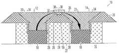
- FIG. 1shows a memory device 10 having first and second electrodes 12 , 14 on an intermetallic dielectric base 16 .
- Each electrodecomprises a lower electrode element 18 , typically comprising tungsten, aluminum, copper, other metals commonly used in integrated circuit manufacturing, or other conductive material, adjacent to base 16 and an upper electrode element 20 , typically made of TiN.
- Electrodes 12 , 14are separated by an electrode separation element 22 .
- Electrode separation elementincludes a lower portion 24 of a separation material, typically a dielectric fill such as silicon dioxide, and an upper portion 26 .
- Upper portion 26has upwardly and inwardly tapering sides 28 , the sides being joined by a surface segment 30 .
- Upper portion 26is made of a dielectric material deposited using high-density plasma (HDP) deposition procedures as discussed below.
- a bridge-type memory material element 32is positioned on the surface segment 30 and extends over and contacts the outer surface 34 of upper electrode element 20 of first and second electrodes 12 , 14 .
- currentflows along an inter-electrode path between first and second electrodes and through memory material element 32 causing the central, active region 38 to change one or more electrical characteristics, such as resistance, upon the application of an appropriate current flow.
- FIGS. 2-9illustrate steps for creating memory device 10 , as well as other memory devices, according to the invention.
- lower electrode elements 18are formed on base 16 and have protective cap elements 40 formed thereon.
- Elements 40are typically made of SiN or another suitable protective material and act as a protective layer for lower electrode elements 18 during subsequent processing steps.
- FIG. 3shows a separation material 42 deposited on the structure of FIG. 2 followed by chemical mechanical polishing (CMP) to create an end surface 44 .
- CMPchemical mechanical polishing
- open regions 46are formed by the removal of elements 40 . Open regions 46 of are bounded by lower electrode elements 18 and inside surfaces 48 of separation material 42 .
- FIG. 5illustrates the result of the HDP CVD deposition of a dielectric material 50 creating cap 26 .
- dielectric material 50is also deposited on side surfaces 48 and lower electrode elements 18 .
- One recipe that can be used to control the ratio of deposition to etching during the HDP CVD process to achieve the desired height, shape and taper anglesis as follows.
- Tapering surfaces 28are illustrated as straight lines in FIG. 5 .
- FIG. 6illustrates an example of generally straight tapering surfaces 28 while
- FIG. 7illustrates stair-stepped tapering surfaces 28 .
- Other types of tapering surfaces 28may also be created.
- FIG. 8illustrates the result of depositing an electrically conductive material 52 onto the structure of FIG. 5 after this etch procedure.
- Material 52may be TiN because of its good compatibility with memory material element 32 ; other appropriate materials may also be used.
- FIG. 9illustrates results of a CMP process to create first and second electrodes 12 , 14 having outer surfaces 54 and surface segment 30 .
- outer surfaces 54 and surface segment 30are coplanar. However, in some cases they need not be coplanar.
- the length 56 of surface segment 30is typically about 10 to 100 nm, and in one embodiment is about 20 nm long.
- the angle between tapering surfaces 28 and the length 56 of surface segment 30affects the amount of chemical mechanical polishing that must be done to the structure of FIG. 8 to achieve the structure of FIG. 9 .
- memory material element 32is formed on surface segment 30 so to contact outer surfaces 54 of first and second electrodes 12 .
- Memory material element 32is typically GST but, as discussed below, memory material element 32 could be made of other materials as well.
- the length of contact between memory material element 32 and surfaces 54should be sufficient to provide effective electrical contact between the surfaces, and to allow for alignment tolerances of the photolithographic process used in patterning the memory material element, without being excessively long.
- the thickness of memory material element 32(the vertical height in FIG. 1 ) is small as is practical given the material chosen and its manner of deposition. For GST, the thickness is typically about 10 to 50 nm, and in one embodiment is about 20 nm.
- the width of memory material element 32(the dimension into the page in FIG. 1 ) is typically about 40 to 100 nm, and again should be as small as practical given the material chosen and the manner in which the pattern is defined; in one embodiment the width of memory material 32 is about 30 ⁇ 100 nm.
- One of the advantages of the present inventionis that the current needed to, for example, change the resistance of memory material element 32 at central region 38 is reduced because the volume of phase change material in the central, active region is very small.
- the inventionfacilitates scaling so that the process should work as critical dimensions on chips shrink.
- Another advantage of the inventionis that two of the dimensions for memory material element 32 , that is length 56 and the thickness (measured in the vertical direction in the figures) of element 32 , are not dependent upon lithographic techniques.
- the location of and length of memory material element 32are typically determined by lithographic techniques, neither is critical because the amount of overlap between memory material 32 and surface 34 of the electrodes can vary within a relatively wide range of distances.
- the length 56 of surface segment 30is not pattern defined, that is not defined by photolithography, and not by etch selectivity, as in the sidewall methods. Rather, length 56 is defined by the CMP process, and the control over the stop point of the CMP.
- Upper electrode elements 20 in the illustrated embodimentare preferably made of TiN. Although other materials, such as TaN, TiAlN or TaAlN, may be used for upper electrode elements 20 , TiN is presently preferred because it makes good contact with CST as memory material element 32 , it is a common material used in semiconductor manufacturing, and it provides a good diffusion barrier at the higher temperatures at which GST-type of memory material transitions, typically in the 600-700° C. range.
- Embodiments of memory device 10include phase change based memory materials, including chalcogenide based materials and other materials, for memory material element 32 .
- Chalcogensinclude any of the four elements oxygen (O), sulfur (S), selenium (Se), and tellurium (Te), forming part of group VI of the periodic table.
- Chalcogenidescomprise compounds of a chalcogen with a more electropositive element or radical.
- Chalcogenide alloyscomprise combinations of chalcogenides with other materials such as transition metals.
- a chalcogenide alloyusually contains one or more elements from column six of the periodic table of elements, such as germanium (Ge) and tin (Sn).
- chalcogenide alloysinclude combinations including one or more of antimony (Sb), gallium (Ga), indium (In), and silver (Ag).
- Many phase change based memory materialshave been described in technical literature, including alloys of: Ga/Sb, In/Sb, In/Se, Sb/Te, Ge/Te, Ge/Sb/Te, In/Sb/Te, Ga/Se/Te, Sn/Sb/Te, In/Sb/Ge, Ag/In/Sb/Te, Ge/Sn/Sb/Te, Ge/Sb/Se/Te and Te/Ge/Sb/S.
- a wide range of alloy compositionsmay be workable.
- the compositionscan be characterized as Te a Ge b Sb100 ⁇ (a+b) .
- Phase change alloysare capable of being switched between a first structural state in which the material is in a generally amorphous solid phase, and a second structural state in which the material is in a generally crystalline solid phase in its local order in the active channel region of the cell. These alloys are at least bistable.
- amorphousis used to refer to a relatively less ordered structure, more disordered than a single crystal, which has the detectable characteristics such as higher electrical resistivity than the crystalline phase.
- crystallineis used to refer to a relatively more ordered structure, more ordered than in an amorphous structure, which has detectable characteristics such as lower electrical resistivity than the amorphous phase.
- phase change materialsmay be electrically switched between different detectable states of local order across the spectrum between completely amorphous and completely crystalline states.
- Other material characteristics affected by the change between amorphous and crystalline phasesinclude atomic order, free electron density and activation energy.
- the materialmay be switched either into different solid phases or into mixtures of two or more solid phases, providing a gray scale between completely amorphous and completely crystalline states.
- the electrical properties in the materialmay vary accordingly.
- Phase change alloyscan be changed from one phase state to another by application of electrical pulses. It has been observed that a shorter, higher amplitude pulse tends to change the phase change material to a generally amorphous state. A longer, lower amplitude pulse tends to change the phase change material to a generally crystalline state. The energy in a shorter, higher amplitude pulse is high enough to allow for bonds of the crystalline structure to be broken and short enough to prevent the atoms from realigning into a crystalline state. Appropriate profiles for pulses can be determined, without undue experimentation, specifically adapted to a particular phase change alloy.
- a material useful for implementation of an RRAM device described hereinis Ge 2 Sb 2 Te 5 , commonly referred to as GST. Other types of phase change materials can also be used.
- phase change materialshave been described with reference to phase change materials.
- other memory materialsalso sometimes referred to as programmable materials, can also be used.
- memory materialsare those materials having electrical properties, such as resistance, that can be changed by the application of energy; the change can be a stepwise change or a continuous change or a combination thereof.
- programmable resistive memory materialsmay be used in other embodiments of the invention, including N 2 doped GST, Ge x Sb y , or other material that uses different crystal phase changes to determine resistance; Pr x Ca y MnO 3 , PrSrMnO, ZrO x , or other material that uses an electrical pulse to change the resistance state; 7,7,8,8-tetracyanoquinodimethane (TCNQ), methanoflillerene 6,6-phenyl C61-butyric acid methyl ester (PCBM), TCNQ-PCBM, Cu-TCNQ, Ag-TCNQ, C 60 -TCNQ, TCNQ doped with other metal, or any other polymer material that has bistable or multi-stable resistance state controlled by an electrical pulse.
- TCNQ7,7,8,8-tetracyanoquinodimethane
- PCBMmethanoflillerene 6,6-phenyl C61-butyric acid methyl ester
- TCNQ-PCBMCu-
- programmable resistive memory materialsinclude GeSbTe, GeSb, NiO, Nb—SrTiO 3 , Ag—GeTe, PrCaMnO, ZnO, Nb 2 O 5 , Cr—SrTiO 3 .
- GeSbTe with dopingsuch as N—, Si—, Ti—, or other element doping may also be used.
- Formation methodBy PVD sputtering or magnetron-sputtering method with reactive gases of Ar, N 2 , and/or He, etc @ the pressure of 1 mtorr ⁇ 100 mtorr.
- the depositionis usually done at room temperature.
- the collimater with aspect ratio of 1 ⁇ 5can be used to improve the fill-in performance.
- the DC bias of several ten to several hundred voltsis also used.
- the combination of DC bias and the collimatercan be used simultaneously.
- the post deposition annealing treatment with vacuum or N2 ambientis sometimes needed to improve the crystallize state of challecogenide material.
- the annealing temperaturetypically ranges 100 C to 400 C with an anneal time of less than 30 minutes.
- challecogenide materialdepends on the design of cell structure.
- a challecogenide material with thickness of higher than 8 nmcan have a phase change characterization so that the material exhibits at least two stable resistance states.
- Another CMR material that includes Mn oxidemay be used.
- Formation methodBy PVD sputtering or magnetron-sputtering method with reactive gases of Ar, N 2 , O 2 , and/or He, etc. at the pressure of 1 mtorr ⁇ 100 mtorr.
- the deposition temperaturecan range from room temperature to ⁇ 600 C, depending on the post deposition treatment condition.
- a collimater with an aspect ratio of 1 ⁇ 5can be used to improve the fill-in performance.
- the DC bias of several ten to several hundred voltsis also used.
- the combination of DC bias and the collimatercan be used simultaneously.
- a magnetic field of several ten gauss to 10,000 gaussmay be applied to improve the magnetic crystallized phase
- the thickness of CMR materialdepends on the design of cell structure.
- the CMR thickness of 10 nm to 200 nmcan be used to be the core material.
- Ni x O yTi x O y ; Al x O y ; W x O y ; Zn x O y ; Zr x O y ; Cu x O y ; etc
- DepositionBy PVD sputtering or magnetron-sputtering method with reactive gases of Ar, N 2 , O 2 , and/or He, etc. at the pressure of 1 mtorr ⁇ 100 mtorr, using a target of metal oxide, such as Ni x O y ; Ti x O y ; Al x O y ; W x O y ; Zn x O y ; Zr x O y ; Cu x O y ; etc.
- the depositionis usually done at room temperature.
- a collimater with an aspect ratio of 1 ⁇ 5can be used to improve the fill-in performance.
- the DC biasof several ten to several hundred volts is also used. If desired, they combination of DC bias and the collimater can be used simultaneously.
- the annealing temperatureranges 400 C to 600 C with an anneal time of less than 2 hours.
- Reactive depositionBy PVD sputtering or magnetron-sputtering method with reactive gases of Ar/O 2 , Ar/N 2 /O 2 , pure O 2 , He/O 2 , He/N 2 /O 2 etc. at the pressure of 1 mtorr ⁇ 100 mtorr, using a target of metal oxide, such as Ni, Ti, Al, W, Zn, Zr, or Cu etc.
- the depositionis usually done at room temperature.
- a collimater with an aspect ratio of 1 ⁇ 5can be used to improve the fill-in performance.
- a DC bias of several ten to several hundred voltsis also used. If desired, the combination of DC bias and the collimater can be used simultaneously.
- OxidationBy a high temperature oxidation system, such as furnace or RTP system.
- the temperatureranges from 200 C to 700 C with pure O 2 or N 2 /O 2 mixed gas at a pressure of several mtorr to 1 atm. The time can range several minute to hours.
- Another oxidation methodis plasma oxidation.
- An RF or a DC source plasma with pure O 2 or Ar/O 2 mixed gas or Ar/N 2 /O 2 mixed gas at a pressure of 1 mtorr to 100 mtorris used to oxidize the surface of metal, such as Ni, Ti, Al, W, Zn, Zr, or Cu etc.
- the oxidation timeranges several seconds to several minutes.
- the oxidation temperatureranges room temperature to 300C, depending on the degree of plasma oxidation.
- EvaporationBy thermal evaporation, e-beam evaporation, or molecular beam epitaxy (MBE) system.
- a solid-state TCNQ and dopent pelletsare co-evaporated in a single chamber.
- the solid-state TCNQ and dopent pelletsare put in a W-boat or a Ta-boat or a ceramic boat.
- a high electrical current or an electron-beamis applied to melt the source so that the materials are mixed and deposited on wafers. There are no reactive chemistries or gases.
- the depositionis done at a pressure of 10-4 torr to 10-10 torr.
- the wafer temperatureranges from room temperature to 200 C.
Landscapes
- Engineering & Computer Science (AREA)
- Manufacturing & Machinery (AREA)
- Chemical & Material Sciences (AREA)
- Materials Engineering (AREA)
- Semiconductor Memories (AREA)
Abstract
Description
1. Field of the Invention
The present invention relates to high density memory devices based on memory materials, for example resistor random access memory (RRAM) devices, the memory material switchable between electrical property states by the application of energy. The memory materials may be phase change based memory materials, including chalcogenide based materials and other materials, and to methods for manufacturing such devices.
2. Description of Related Art
Phase change based memory materials are widely used in read-write optical disks. These materials have at least two solid phases, including for example a generally amorphous solid phase and a generally crystalline solid phase. Laser pulses are used in read-write optical disks to switch between phases and to read the optical properties of the material after the phase change.
Phase change based memory materials, like chalcogenide based materials and similar materials, also can be caused to change phase by application of electrical current at levels suitable for implementation in integrated circuits. The generally amorphous state is characterized by higher resistivity than the generally crystalline state; this difference in resistance can be readily sensed to indicate data. These properties have generated interest in using programmable resistive material to form nonvolatile memory circuits, which can be read and written with random access.
The change from the amorphous to the crystalline state is generally a lower current operation. The change from crystalline to amorphous, referred to as reset herein, is generally a higher current operation, which includes a short high current density pulse to melt or breakdown the crystalline structure, after which the phase change material cools quickly, quenching the phase change process, allowing at least a portion of the phase change structure to stabilize in the amorphous state. It is desirable to minimize the magnitude of the reset current used to cause transition of phase change material from crystalline state to amorphous state. The magnitude of the reset current needed for reset can be reduced by reducing the size of the phase change material element in the cell and by reducing the size of the contact area between electrodes and the phase change material, so that higher current densities are achieved with small absolute current values through the phase change material element.
One direction of development has been toward forming small pores in an integrated circuit structure, and using small quantities of programmable resistive material to fill the small pores. Patents illustrating development toward small pores include: Ovshinsky, “Multibit Single Cell Memory Element Having Tapered Contact,” U.S. Pat. No. 5,687,112, issued Nov. 11, 1997; Zahorik et al., “Method of Making Chalogenide [sic] Memory Device,” U.S. Pat. No. 5,789,277, issued Aug. 4, 1998; Doan et al., “Controllable Ovonic Phase-Change Semiconductor Memory Device and Methods of Fabricating the Same,” U.S. Pat. No. 6,150,253, issued Nov. 21, 2000.
Problems have arisen in manufacturing such devices with very small dimensions, and with variations in process that meet tight specifications needed for large-scale memory devices. It is desirable therefore to provide a memory cell structure having small dimensions and low reset currents, and a method for manufacturing such structure.
A first aspect of the invention is directed to a memory device comprising first and second electrodes having first and second outer surfaces. The memory device also comprises an electrode-separating, insulating member between the first and second electrodes. The insulating member comprises upwardly and inwardly tapering surfaces connected by a surface segment. The surface segment has a length between the tapering surfaces near the first and second outer surfaces. The memory device also comprises a bridge across the surface segment of the insulating member. The bridge contacts the first and second outer surfaces and defines an inter-electrode path between the first and second electrodes and across the insulating member. The inter-electrode path has a path length defined at least in part by the length of the surface segment. The bridge comprises memory material switchable between electrical property states by the application of energy. In some embodiments the bridge comprises a phase change material. The insulating member may comprise an outer portion, the outer portion comprising a high density plasma-deposited separation material.
A second aspect of the invention is directed to a method for making a memory device of the type including a bridge-type memory material element switchable between electrical property states by the application of energy. An electrode structure, comprising first and second electrode elements separated by a separation material, is formed. A dielectric material is deposited onto an end surface of the separation material using a high density plasma (HDP) deposition procedure. The deposition of the dielectric material is controlled to create a dielectric material cap on the end surface, the dielectric material cap having upwardly and inwardly tapering surfaces. An electrically conductive material is deposited to contact the electrode elements and to extend along the tapering sides of the dielectric material thus creating first and second electrodes. The electrically conductive material and the dielectric material cap are planarized to create first and second outer surfaces on the first and second electrodes and a surface segment on the dielectric material. The surface segment connects the tapering sides and has a length measured between the tapering sides. At least one of the dielectric material depositing step and the planarizing step is controlled so that the length is within a chosen dimensional range. A bridge-type memory material element is formed over the surface segment and in electrical contact with portions of the first and second outer surfaces. Energy passing along an inter-electrode path between the first and second electrodes and across the surface segment of the dielectric member is concentrated within the memory material element so to facilitate changing an electrical property state of the memory material element.
The method described herein for formation of a memory cell device and, for example, in an RRAM device, can be used to make small phase change gates, bridges or similar structures for other devices.
Various features and advantages of the invention will appear from the following description in which the preferred embodiments have been set forth in detail in conjunction with the accompanying drawings.
The following description of the invention will typically be with reference to specific structural embodiments and methods. It is to be understood that there is no intention to limit the invention to the specifically disclosed embodiments and methods but that the invention may be practiced using other features, elements, methods and embodiments. Like elements in various embodiments are commonly referred to with like reference numerals.
During HDP CVD deposition both deposition and etching occurs to create the characteristic triangular shape with upwardly and inwardly tapering surfaces. General information on the HDP process can be found in the textbook “Introduction to Semiconductor Manufacturing Technology” inchapter 10 Section 7 (10.7).
One recipe that can be used to control the ratio of deposition to etching during the HDP CVD process to achieve the desired height, shape and taper angles is as follows.
- 1. SiH4: 95sccm/Ar: 390sccm/O2: 150sccm/Plasma Heat˜300C/Top plasma power 3550W/Bottom Plasma power 2700W/He: 8sccm.
- 2. The Etch/dep ratio of HDP process could be controlled by Top plasma power & Bottom Plasma Power. Higher Plasma power will increase the plasma etch rate and increase the Etch/dep ratio because plasma Etch is enhanced.
Tapering surfaces28 are illustrated as straight lines inFIG. 5 .FIG. 6 illustrates an example of generally straight tapering surfaces28 whileFIG. 7 illustrates stair-stepped tapering surfaces28. Other types of taperingsurfaces 28 may also be created.
Thedielectric material 50 coveringlower electrode elements 18 is etched to expose thelower electrode elements 18. This is preferably accomplished using a slightly anisotropic etch procedure.FIG. 8 illustrates the result of depositing an electricallyconductive material 52 onto the structure ofFIG. 5 after this etch procedure.Material 52 may be TiN because of its good compatibility withmemory material element 32; other appropriate materials may also be used.FIG. 9 illustrates results of a CMP process to create first andsecond electrodes 12,14 having outer surfaces54 andsurface segment 30. In the preferred embodiment outer surfaces54 andsurface segment 30 are coplanar. However, in some cases they need not be coplanar. Thelength 56 ofsurface segment 30 is typically about 10 to 100 nm, and in one embodiment is about 20 nm long. The angle between taperingsurfaces 28 and thelength 56 ofsurface segment 30 affects the amount of chemical mechanical polishing that must be done to the structure ofFIG. 8 to achieve the structure ofFIG. 9 .
Thereaftermemory material element 32, seeFIG. 1 , is formed onsurface segment 30 so to contact outer surfaces54 of first andsecond electrodes 12.Memory material element 32 is typically GST but, as discussed below,memory material element 32 could be made of other materials as well. The length of contact betweenmemory material element 32 and surfaces54 should be sufficient to provide effective electrical contact between the surfaces, and to allow for alignment tolerances of the photolithographic process used in patterning the memory material element, without being excessively long. The thickness of memory material element32 (the vertical height inFIG. 1 ) is small as is practical given the material chosen and its manner of deposition. For GST, the thickness is typically about 10 to 50 nm, and in one embodiment is about 20 nm. The width of memory material element32 (the dimension into the page inFIG. 1 ) is typically about 40 to 100 nm, and again should be as small as practical given the material chosen and the manner in which the pattern is defined; in one embodiment the width ofmemory material 32 is about 30˜100 nm.
One of the advantages of the present invention is that the current needed to, for example, change the resistance ofmemory material element 32 at central region38 is reduced because the volume of phase change material in the central, active region is very small. The invention facilitates scaling so that the process should work as critical dimensions on chips shrink.
Another advantage of the invention is that two of the dimensions formemory material element 32, that islength 56 and the thickness (measured in the vertical direction in the figures) ofelement 32, are not dependent upon lithographic techniques. In addition, while the location of and length ofmemory material element 32 are typically determined by lithographic techniques, neither is critical because the amount of overlap betweenmemory material 32 andsurface 34 of the electrodes can vary within a relatively wide range of distances.
Thelength 56 ofsurface segment 30 is not pattern defined, that is not defined by photolithography, and not by etch selectivity, as in the sidewall methods. Rather,length 56 is defined by the CMP process, and the control over the stop point of the CMP.
Embodiments ofmemory device 10 include phase change based memory materials, including chalcogenide based materials and other materials, formemory material element 32. Chalcogens include any of the four elements oxygen (O), sulfur (S), selenium (Se), and tellurium (Te), forming part of group VI of the periodic table. Chalcogenides comprise compounds of a chalcogen with a more electropositive element or radical. Chalcogenide alloys comprise combinations of chalcogenides with other materials such as transition metals. A chalcogenide alloy usually contains one or more elements from column six of the periodic table of elements, such as germanium (Ge) and tin (Sn). Often, chalcogenide alloys include combinations including one or more of antimony (Sb), gallium (Ga), indium (In), and silver (Ag). Many phase change based memory materials have been described in technical literature, including alloys of: Ga/Sb, In/Sb, In/Se, Sb/Te, Ge/Te, Ge/Sb/Te, In/Sb/Te, Ga/Se/Te, Sn/Sb/Te, In/Sb/Ge, Ag/In/Sb/Te, Ge/Sn/Sb/Te, Ge/Sb/Se/Te and Te/Ge/Sb/S. In the family of Ge/Sb/Te alloys, a wide range of alloy compositions may be workable. The compositions can be characterized as TeaGebSb100−(a+b).
One researcher has described the most useful alloys as having an average concentration of Te in the deposited materials well below 70%, typically below about 60% and ranged in general from as low as about 23% up to about 58% Te and most preferably about 48% to 58% Te. Concentrations of Ge were above about 5% and ranged from a low of about 8% to about 30% average in the material, remaining generally below 50%. Most preferably, concentrations of Ge ranged from about 8% to about 40%. The remainder of the principal constituent elements in this composition was Sb. These percentages are atomic percentages that total 100% of the atoms of the constituent elements. (Ovshinsky '112 patent, columns 10-11.) Particular alloys evaluated by another researcher include Ge2Sb2Te5, GeSb2Te4and GeSb4Te7. (Noboru Yamada, “Potential of Ge—Sb—Te Phase-Change Optical Disks for High-Data-Rate Recording”, SPIE v. 3109, pp. 28-37 (1997).) More generally, a transition metal such as chromium (Cr), iron (Fe), nickel (Ni), niobium Nb), palladium (Pd), platinum (Pt) and mixtures or alloys thereof may be combined with Ge/Sb/Te to form a phase change alloy that has programmable resistive properties. Specific examples of memory materials that may be useful are given in Ovshinsky '112 at columns 11-13, which examples are hereby incorporated by reference.
Phase change alloys are capable of being switched between a first structural state in which the material is in a generally amorphous solid phase, and a second structural state in which the material is in a generally crystalline solid phase in its local order in the active channel region of the cell. These alloys are at least bistable. The term amorphous is used to refer to a relatively less ordered structure, more disordered than a single crystal, which has the detectable characteristics such as higher electrical resistivity than the crystalline phase. The term crystalline is used to refer to a relatively more ordered structure, more ordered than in an amorphous structure, which has detectable characteristics such as lower electrical resistivity than the amorphous phase. Typically, phase change materials may be electrically switched between different detectable states of local order across the spectrum between completely amorphous and completely crystalline states. Other material characteristics affected by the change between amorphous and crystalline phases include atomic order, free electron density and activation energy. The material may be switched either into different solid phases or into mixtures of two or more solid phases, providing a gray scale between completely amorphous and completely crystalline states. The electrical properties in the material may vary accordingly.
Phase change alloys can be changed from one phase state to another by application of electrical pulses. It has been observed that a shorter, higher amplitude pulse tends to change the phase change material to a generally amorphous state. A longer, lower amplitude pulse tends to change the phase change material to a generally crystalline state. The energy in a shorter, higher amplitude pulse is high enough to allow for bonds of the crystalline structure to be broken and short enough to prevent the atoms from realigning into a crystalline state. Appropriate profiles for pulses can be determined, without undue experimentation, specifically adapted to a particular phase change alloy. A material useful for implementation of an RRAM device described herein is Ge2Sb2Te5, commonly referred to as GST. Other types of phase change materials can also be used.
The invention has been described with reference to phase change materials. However, other memory materials, also sometimes referred to as programmable materials, can also be used. As used in this application, memory materials are those materials having electrical properties, such as resistance, that can be changed by the application of energy; the change can be a stepwise change or a continuous change or a combination thereof. Other programmable resistive memory materials may be used in other embodiments of the invention, including N2doped GST, GexSby, or other material that uses different crystal phase changes to determine resistance; PrxCayMnO3, PrSrMnO, ZrOx, or other material that uses an electrical pulse to change the resistance state; 7,7,8,8-tetracyanoquinodimethane (TCNQ), methanoflillerene 6,6-phenyl C61-butyric acid methyl ester (PCBM), TCNQ-PCBM, Cu-TCNQ, Ag-TCNQ, C60-TCNQ, TCNQ doped with other metal, or any other polymer material that has bistable or multi-stable resistance state controlled by an electrical pulse. Further examples of programmable resistive memory materials include GeSbTe, GeSb, NiO, Nb—SrTiO3, Ag—GeTe, PrCaMnO, ZnO, Nb2O5, Cr—SrTiO3.
The following are short summaries describing four types of resistive memory materials.
1. Challecogenide Material
GexSbyTez
x:y:z=2:2:5
Or other compositions with x: 0˜5; y: 0˜5; z: 0˜10
GeSbTe with doping, such as N—, Si—, Ti—, or other element doping may also be used.
Formation method: By PVD sputtering or magnetron-sputtering method with reactive gases of Ar, N2, and/or He, etc @ the pressure of 1 mtorr˜100 mtorr. The deposition is usually done at room temperature. The collimater with aspect ratio of 1˜5 can be used to improve the fill-in performance. To improve the fill-in performance, the DC bias of several ten to several hundred volts is also used. On the other hand, the combination of DC bias and the collimater can be used simultaneously.
The post deposition annealing treatment with vacuum or N2 ambient is sometimes needed to improve the crystallize state of challecogenide material. The annealing temperature typically ranges 100 C to 400 C with an anneal time of less than 30 minutes.
The thickness of challecogenide material depends on the design of cell structure. In general, a challecogenide material with thickness of higher than 8 nm can have a phase change characterization so that the material exhibits at least two stable resistance states.
2. CMR (Colossal Magnetoresistance) Material
PrxCayMnO3
x:y=0.5:0.5
Or other compositions with x: 0˜1; y: 0˜1
Another CMR material that includes Mn oxide may be used
Formation method: By PVD sputtering or magnetron-sputtering method with reactive gases of Ar, N2, O2, and/or He, etc. at the pressure of 1 mtorr˜100 mtorr. The deposition temperature can range from room temperature to ˜600 C, depending on the post deposition treatment condition. A collimater with an aspect ratio of 1˜5 can be used to improve the fill-in performance. To improve the fill-in performance, the DC bias of several ten to several hundred volts is also used. On the other hand, the combination of DC bias and the collimater can be used simultaneously. A magnetic field of several ten gauss to 10,000 gauss may be applied to improve the magnetic crystallized phase
- The post deposition annealing treatment with vacuum or N2ambient or O2/N2mixed ambient may be needed to improve the crystallized state of CMR material. The annealing temperature typically ranges 400 C to 600 C with an anneal time of less than 2 hours.
The thickness of CMR material depends on the design of cell structure. The CMR thickness of 10 nm to 200 nm can be used to be the core material.
- A buffer layer of YBCO (YBaCuO3, a kind of high temperature superconductor material) is often used to improve the crystallized state of CMR material. The YBCO is deposited before the deposition of CMR material. The thickness of YBCO ranges 30 nm to 200 nm.
3. 2-Element Compound
NixOy; TixOy; AlxOy; WxOy; ZnxOy; ZrxOy; CuxOy; etc
x:y=0.5:0.5
Other compositions with x: 0˜1; y: 0˜1
Formation Method:
1. Deposition: By PVD sputtering or magnetron-sputtering method with reactive gases of Ar, N2, O2, and/or He, etc. at the pressure of 1 mtorr˜100 mtorr, using a target of metal oxide, such as NixOy; TixOy; AlxOy; WxOy; ZnxOy; ZrxOy; CuxOy; etc. The deposition is usually done at room temperature. A collimater with an aspect ratio of 1˜5 can be used to improve the fill-in performance. To improve the fill-in performance, the DC bias of several ten to several hundred volts is also used. If desired, they combination of DC bias and the collimater can be used simultaneously.
The post deposition annealing treatment with vacuum or N2ambient or O2/N2mixed ambient as sometimes needed to improve the oxygen distribution of metal oxide. The annealing temperature ranges 400 C to 600 C with an anneal time of less than 2 hours.
2. Reactive deposition: By PVD sputtering or magnetron-sputtering method with reactive gases of Ar/O2, Ar/N2/O2, pure O2, He/O2, He/N2/O2etc. at the pressure of 1 mtorr˜100 mtorr, using a target of metal oxide, such as Ni, Ti, Al, W, Zn, Zr, or Cu etc. The deposition is usually done at room temperature. A collimater with an aspect ratio of 1˜5 can be used to improve the fill-in performance. To improve the fill-in performance, a DC bias of several ten to several hundred volts is also used. If desired, the combination of DC bias and the collimater can be used simultaneously.
- The post deposition annealing treatment with vacuum or N2ambient or O2/N2mixed ambient is sometimes needed to improve the oxygen distribution of metal oxide. The annealing temperature ranges 400 C to 600 C with an anneal time of less than 2 hours.
3. Oxidation: By a high temperature oxidation system, such as furnace or RTP system. The temperature ranges from 200 C to 700 C with pure O2or N2/O2mixed gas at a pressure of several mtorr to 1 atm. The time can range several minute to hours. Another oxidation method is plasma oxidation. An RF or a DC source plasma with pure O2or Ar/O2mixed gas or Ar/N2/O2mixed gas at a pressure of 1 mtorr to 100 mtorr is used to oxidize the surface of metal, such as Ni, Ti, Al, W, Zn, Zr, or Cu etc. The oxidation time ranges several seconds to several minutes. The oxidation temperature ranges room temperature to 300C, depending on the degree of plasma oxidation.
4. Polymer Material
TCNQ with doping of Cu, C60, Ag etc.
PCBM-TCNQ mixed polymer
Formation Method:
1. Evaporation: By thermal evaporation, e-beam evaporation, or molecular beam epitaxy (MBE) system. A solid-state TCNQ and dopent pellets are co-evaporated in a single chamber. The solid-state TCNQ and dopent pellets are put in a W-boat or a Ta-boat or a ceramic boat. A high electrical current or an electron-beam is applied to melt the source so that the materials are mixed and deposited on wafers. There are no reactive chemistries or gases. The deposition is done at a pressure of 10-4 torr to 10-10 torr. The wafer temperature ranges from room temperature to 200 C.
- The post deposition annealing treatment with vacuum or N2ambient is sometimes needed to improve the composition distribution of polymer material. The annealing temperature ranges room temperature to 300 C with an anneal time of less than 1 hour.
2. Spin-coat: By a spin-coater with the doped-TCNQ solution @ the rotation of less than 1000 rpm. After spin-coating, the wafer is put to wait the solid-state formation @ room temperature or temperature of less than 200 C. The waiting time ranges from several minutes to days, depending on the temperature and on the formation conditions.
For additional information on the manufacture, component materials, use and operation of phase change random access memory devices, see U.S. patent application Ser. No. 11/155,067, filed 17 Jun. 2005, entitled Thin Film Fuse Phase Change Ram And Manufacturing Method.
The above descriptions may have used terms such as above, below, top, bottom, over, under, et cetera. These terms are used to aid understanding of the invention are not used in a limiting sense.
While the present invention is disclosed by reference to the preferred embodiments and examples detailed above, it is to be understood that these examples are intended in an illustrative rather than in a limiting sense. It is contemplated that modifications and combinations will occur to those skilled in the art, which modifications and combinations will be within the spirit of the invention and the scope of the following claims.
Any and all patents, patent applications and printed publications referred to above are hereby incorporated by reference.
Claims (11)
1. A memory device, comprising:
a first electrode having a first outer surface,
a second electrode having a second outer surface;
an electrode-separating, insulating member between the first electrode and the second electrode,
the insulating member comprising upwardly and inwardly tapering surfaces connected by a surface segment;
portions of the first and second electrodes overlying the upwardly and inwardly tapering surfaces;
the surface segment having a length between the tapering surfaces near the first and second outer surfaces; and
a bridge across the surface segment of the insulating member, the bridge contacting the first and second outer surfaces and defining an inter-electrode path between the first and second electrodes and across the insulating member, the inter-electrode path having a path length defined at least in part by the length of the surface segment, the bridge comprising memory material switchable between electrical property states by the application of energy.
2. The memory device according toclaim 1 wherein the bridge comprises a phase change material.
3. The memory device according toclaim 1 wherein the first and second electrodes comprise TiN at the first and second outer surfaces contacting the bridge.
4. The memory device according toclaim 1 wherein the insulating member comprises an outer portion, the outer portion comprising a high density plasma-deposited separation material.
5. The memory device according to claim l wherein the first and second electrodes contact the tapering surfaces and extend to the surface segment.
6. The memory device according toclaim 1 wherein the tapering surfaces are generally straight surfaces.
7. The memory device according toclaim 1 wherein the tapering surfaces are generally stair stepped surfaces.
8. The memory device according toclaim 1 wherein the first and second outer surfaces and the surface segment are generally coplanar.
9. The memory device according toclaim 1 wherein the bridge contacts the surface segment and the portions of the first and second outer surfaces.
10. The memory cell device according toclaim 1 wherein the resistance of the bridge changes when the electrical property state of the bridge changes.
11. The memory cell device according toclaim 1 wherein the first and second surfaces and the surface segment are generally coplanar.
Priority Applications (2)
| Application Number | Priority Date | Filing Date | Title |
|---|---|---|---|
| US11/279,945US7554144B2 (en) | 2006-04-17 | 2006-04-17 | Memory device and manufacturing method |
| US12/469,184US7972893B2 (en) | 2006-04-17 | 2009-05-20 | Memory device manufacturing method |
Applications Claiming Priority (1)
| Application Number | Priority Date | Filing Date | Title |
|---|---|---|---|
| US11/279,945US7554144B2 (en) | 2006-04-17 | 2006-04-17 | Memory device and manufacturing method |
Related Child Applications (1)
| Application Number | Title | Priority Date | Filing Date |
|---|---|---|---|
| US12/469,184DivisionUS7972893B2 (en) | 2006-04-17 | 2009-05-20 | Memory device manufacturing method |
Publications (2)
| Publication Number | Publication Date |
|---|---|
| US20070241371A1 US20070241371A1 (en) | 2007-10-18 |
| US7554144B2true US7554144B2 (en) | 2009-06-30 |
Family
ID=38604023
Family Applications (2)
| Application Number | Title | Priority Date | Filing Date |
|---|---|---|---|
| US11/279,945Active2026-06-27US7554144B2 (en) | 2006-04-17 | 2006-04-17 | Memory device and manufacturing method |
| US12/469,184ActiveUS7972893B2 (en) | 2006-04-17 | 2009-05-20 | Memory device manufacturing method |
Family Applications After (1)
| Application Number | Title | Priority Date | Filing Date |
|---|---|---|---|
| US12/469,184ActiveUS7972893B2 (en) | 2006-04-17 | 2009-05-20 | Memory device manufacturing method |
Country Status (1)
| Country | Link |
|---|---|
| US (2) | US7554144B2 (en) |
Cited By (6)
| Publication number | Priority date | Publication date | Assignee | Title |
|---|---|---|---|---|
| US20090218557A1 (en)* | 2008-03-03 | 2009-09-03 | Elpida Memory, Inc. | Phase change memory device and fabrication method thereof |
| US20090239358A1 (en)* | 2006-04-17 | 2009-09-24 | Macronix International Co., Ltd. | Memory Device Manufacturing Method |
| US20090278258A1 (en)* | 2008-05-06 | 2009-11-12 | International Business Machines Corporation | Interconnect structure with a mushroom-shaped oxide capping layer and method for fabricating same |
| US20100032636A1 (en)* | 2008-08-05 | 2010-02-11 | Seagate Technology Llc | Non-volatile memory cell with enhanced filament formation characteristics |
| US20110147689A1 (en)* | 2009-12-22 | 2011-06-23 | Hynix Semiconductor Inc. | Phase change memory device capable of reducing disturbance and fabrication method thereof |
| US9741918B2 (en) | 2013-10-07 | 2017-08-22 | Hypres, Inc. | Method for increasing the integration level of superconducting electronics circuits, and a resulting circuit |
Families Citing this family (1)
| Publication number | Priority date | Publication date | Assignee | Title |
|---|---|---|---|---|
| US7852658B2 (en)* | 2008-03-14 | 2010-12-14 | Micron Technology, Inc. | Phase change memory cell with constriction structure |
Citations (159)
| Publication number | Priority date | Publication date | Assignee | Title |
|---|---|---|---|---|
| US3271591A (en) | 1963-09-20 | 1966-09-06 | Energy Conversion Devices Inc | Symmetrical current controlling device |
| US3530441A (en) | 1969-01-15 | 1970-09-22 | Energy Conversion Devices Inc | Method and apparatus for storing and retrieving information |
| US4599705A (en) | 1979-12-13 | 1986-07-08 | Energy Conversion Devices, Inc. | Programmable cell for use in programmable electronic arrays |
| US4719594A (en) | 1984-11-01 | 1988-01-12 | Energy Conversion Devices, Inc. | Grooved optical data storage device including a chalcogenide memory layer |
| US4876220A (en) | 1986-05-16 | 1989-10-24 | Actel Corporation | Method of making programmable low impedance interconnect diode element |
| US4959812A (en) | 1987-12-28 | 1990-09-25 | Kabushiki Kaisha Toshiba | Electrically erasable programmable read-only memory with NAND cell structure |
| US5166096A (en) | 1991-10-29 | 1992-11-24 | International Business Machines Corporation | Process for fabricating self-aligned contact studs for semiconductor structures |
| US5166758A (en) | 1991-01-18 | 1992-11-24 | Energy Conversion Devices, Inc. | Electrically erasable phase change memory |
| US5177567A (en) | 1991-07-19 | 1993-01-05 | Energy Conversion Devices, Inc. | Thin-film structure for chalcogenide electrical switching devices and process therefor |
| US5332923A (en) | 1991-08-06 | 1994-07-26 | Nec Corporation | Semiconductor memory |
| US5391901A (en) | 1992-10-30 | 1995-02-21 | Nec Corporation | Semiconductor memory with oblique folded bit-line arrangement |
| US5515488A (en) | 1994-08-30 | 1996-05-07 | Xerox Corporation | Method and apparatus for concurrent graphical visualization of a database search and its search history |
| US5534712A (en) | 1991-01-18 | 1996-07-09 | Energy Conversion Devices, Inc. | Electrically erasable memory elements characterized by reduced current and improved thermal stability |
| US5687112A (en)* | 1996-04-19 | 1997-11-11 | Energy Conversion Devices, Inc. | Multibit single cell memory element having tapered contact |
| US5789758A (en) | 1995-06-07 | 1998-08-04 | Micron Technology, Inc. | Chalcogenide memory cell with a plurality of chalcogenide electrodes |
| US5789277A (en) | 1996-07-22 | 1998-08-04 | Micron Technology, Inc. | Method of making chalogenide memory device |
| US5814527A (en) | 1996-07-22 | 1998-09-29 | Micron Technology, Inc. | Method of making small pores defined by a disposable internal spacer for use in chalcogenide memories |
| US5831276A (en) | 1995-06-07 | 1998-11-03 | Micron Technology, Inc. | Three-dimensional container diode for use with multi-state material in a non-volatile memory cell |
| US5837564A (en) | 1995-11-01 | 1998-11-17 | Micron Technology, Inc. | Method for optimal crystallization to obtain high electrical performance from chalcogenides |
| US5869843A (en) | 1995-06-07 | 1999-02-09 | Micron Technology, Inc. | Memory array having a multi-state element and method for forming such array or cells thereof |
| US5879955A (en) | 1995-06-07 | 1999-03-09 | Micron Technology, Inc. | Method for fabricating an array of ultra-small pores for chalcogenide memory cells |
| US5902704A (en) | 1997-07-02 | 1999-05-11 | Lsi Logic Corporation | Process for forming photoresist mask over integrated circuit structures with critical dimension control |
| US5952671A (en) | 1997-05-09 | 1999-09-14 | Micron Technology, Inc. | Small electrode for a chalcogenide switching device and method for fabricating same |
| US5958358A (en) | 1992-07-08 | 1999-09-28 | Yeda Research And Development Co., Ltd. | Oriented polycrystalline thin films of transition metal chalcogenides |
| US5970336A (en) | 1996-08-22 | 1999-10-19 | Micron Technology, Inc. | Method of making memory cell incorporating a chalcogenide element |
| US5985698A (en) | 1996-07-22 | 1999-11-16 | Micron Technology, Inc. | Fabrication of three dimensional container diode for use with multi-state material in a non-volatile memory cell |
| US6011725A (en) | 1997-08-01 | 2000-01-04 | Saifun Semiconductors, Ltd. | Two bit non-volatile electrically erasable and programmable semiconductor memory cell utilizing asymmetrical charge trapping |
| US6025220A (en) | 1996-06-18 | 2000-02-15 | Micron Technology, Inc. | Method of forming a polysilicon diode and devices incorporating such diode |
| US6031287A (en) | 1997-06-18 | 2000-02-29 | Micron Technology, Inc. | Contact structure and memory element incorporating the same |
| US6034882A (en) | 1998-11-16 | 2000-03-07 | Matrix Semiconductor, Inc. | Vertically stacked field programmable nonvolatile memory and method of fabrication |
| US6066870A (en) | 1996-07-16 | 2000-05-23 | Micron Technology, Inc. | Single digit line with cell contact interconnect |
| US6077674A (en) | 1999-10-27 | 2000-06-20 | Agilent Technologies Inc. | Method of producing oligonucleotide arrays with features of high purity |
| US6087269A (en) | 1998-04-20 | 2000-07-11 | Advanced Micro Devices, Inc. | Method of making an interconnect using a tungsten hard mask |
| US6087674A (en) | 1996-10-28 | 2000-07-11 | Energy Conversion Devices, Inc. | Memory element with memory material comprising phase-change material and dielectric material |
| WO2000045108A1 (en) | 1999-01-28 | 2000-08-03 | Heckler & Koch Gmbh | Locked breech for a semi-automatic small arm with a breech head and a breech carrier and a resilient annular catch with longitudinal slot |
| US6114713A (en) | 1997-01-28 | 2000-09-05 | Zahorik; Russell C. | Integrated circuit memory cell having a small active area and method of forming same |
| US6117720A (en) | 1995-06-07 | 2000-09-12 | Micron Technology, Inc. | Method of making an integrated circuit electrode having a reduced contact area |
| US6147395A (en) | 1996-10-02 | 2000-11-14 | Micron Technology, Inc. | Method for fabricating a small area of contact between electrodes |
| WO2000079539A1 (en) | 1999-06-22 | 2000-12-28 | Ovonyx, Inc. | Method of programming phase-change memory element |
| US6177317B1 (en) | 1999-04-14 | 2001-01-23 | Macronix International Co., Ltd. | Method of making nonvolatile memory devices having reduced resistance diffusion regions |
| WO2001045108A1 (en) | 1999-12-16 | 2001-06-21 | Ovonyx, Inc. | Programmable resistance memory arrays with reference cells |
| US6271090B1 (en) | 2000-12-22 | 2001-08-07 | Macronix International Co., Ltd. | Method for manufacturing flash memory device with dual floating gates and two bits per cell |
| US6280684B1 (en) | 1994-12-13 | 2001-08-28 | Ricoh Company, Ltd. | Sputtering target, method of producing the target, optical recording medium fabricated by using the sputtering target, and method of fabricating the optical recording medium |
| US6320786B1 (en) | 2000-12-22 | 2001-11-20 | Macronix International Co., Ltd. | Method of controlling multi-state NROM |
| US20010055838A1 (en) | 2000-04-28 | 2001-12-27 | Matrix Semiconductor Inc. | Nonvolatile memory on SOI and compound semiconductor substrates and method of fabrication |
| US6339544B1 (en) | 2000-09-29 | 2002-01-15 | Intel Corporation | Method to enhance performance of thermal resistor device |
| US6351406B1 (en) | 1998-11-16 | 2002-02-26 | Matrix Semiconductor, Inc. | Vertically stacked field programmable nonvolatile memory and method of fabrication |
| US6372651B1 (en) | 1998-07-17 | 2002-04-16 | Advanced Micro Devices, Inc. | Method for trimming a photoresist pattern line for memory gate etching |
| US20020081833A1 (en) | 2000-12-22 | 2002-06-27 | Li Calvin K. | Patterning three dimensional structures |
| US6420215B1 (en) | 2000-04-28 | 2002-07-16 | Matrix Semiconductor, Inc. | Three-dimensional memory array and method of fabrication |
| US6420216B1 (en) | 2000-03-14 | 2002-07-16 | International Business Machines Corporation | Fuse processing using dielectric planarization pillars |
| US6429064B1 (en) | 2000-09-29 | 2002-08-06 | Intel Corporation | Reduced contact area of sidewall conductor |
| US6483736B2 (en) | 1998-11-16 | 2002-11-19 | Matrix Semiconductor, Inc. | Vertically stacked field programmable nonvolatile memory and method of fabrication |
| US6487114B2 (en) | 2001-02-28 | 2002-11-26 | Macronix International Co., Ltd. | Method of reading two-bit memories of NROM cell |
| US20020182835A1 (en) | 2001-05-29 | 2002-12-05 | Quinn Robert M. | Method for manufacturing contacts for a Chalcogenide memory device |
| US6501111B1 (en) | 2000-06-30 | 2002-12-31 | Intel Corporation | Three-dimensional (3D) programmable device |
| US6511867B2 (en) | 2001-06-30 | 2003-01-28 | Ovonyx, Inc. | Utilizing atomic layer deposition for programmable device |
| US6512241B1 (en) | 2001-12-31 | 2003-01-28 | Intel Corporation | Phase change material memory device |
| US6534781B2 (en) | 2000-12-26 | 2003-03-18 | Ovonyx, Inc. | Phase-change memory bipolar array utilizing a single shallow trench isolation for creating an individual active area region for two memory array elements and one bipolar base contact |
| US6545903B1 (en) | 2001-12-17 | 2003-04-08 | Texas Instruments Incorporated | Self-aligned resistive plugs for forming memory cell with phase change material |
| US6555860B2 (en) | 2000-09-29 | 2003-04-29 | Intel Corporation | Compositionally modified resistive electrode |
| US6563156B2 (en) | 2001-03-15 | 2003-05-13 | Micron Technology, Inc. | Memory elements and methods for making same |
| US6567293B1 (en) | 2000-09-29 | 2003-05-20 | Ovonyx, Inc. | Single level metal memory cell using chalcogenide cladding |
| US6566700B2 (en) | 2001-10-11 | 2003-05-20 | Ovonyx, Inc. | Carbon-containing interfacial layer for phase-change memory |
| US6579760B1 (en) | 2002-03-28 | 2003-06-17 | Macronix International Co., Ltd. | Self-aligned, programmable phase change memory |
| US6586761B2 (en) | 2001-09-07 | 2003-07-01 | Intel Corporation | Phase change material memory device |
| US6589714B2 (en) | 2001-06-26 | 2003-07-08 | Ovonyx, Inc. | Method for making programmable resistance memory element using silylated photoresist |
| US6605527B2 (en) | 2001-06-30 | 2003-08-12 | Intel Corporation | Reduced area intersection between electrode and programming element |
| US6605821B1 (en) | 2002-05-10 | 2003-08-12 | Hewlett-Packard Development Company, L.P. | Phase change material electronic memory structure and method for forming |
| US6607974B2 (en) | 2000-07-14 | 2003-08-19 | Micron Technology, Inc. | Method of forming a contact structure in a semiconductor device |
| US6613604B2 (en) | 2001-08-02 | 2003-09-02 | Ovonyx, Inc. | Method for making small pore for use in programmable resistance memory element |
| US6617192B1 (en)* | 1997-10-01 | 2003-09-09 | Ovonyx, Inc. | Electrically programmable memory element with multi-regioned contact |
| US6620715B1 (en) | 2002-03-29 | 2003-09-16 | Cypress Semiconductor Corp. | Method for forming sub-critical dimension structures in an integrated circuit |
| US6639849B2 (en) | 2002-02-28 | 2003-10-28 | Fujitsu Limited | Nonvolatile semiconductor memory device programming second dynamic reference cell according to threshold value of first dynamic reference cell |
| US6673700B2 (en) | 2001-06-30 | 2004-01-06 | Ovonyx, Inc. | Reduced area intersection between electrode and programming element |
| US20040051161A1 (en)* | 2002-04-09 | 2004-03-18 | Matsushita Electric Industrial Co., Ltd. | Non-volatile memory and the fabrication method thereof |
| US20040051094A1 (en) | 2002-09-13 | 2004-03-18 | Mitsubishi Denki Kabushiki Kaisha | Non-volatile semiconductor memory device allowing shrinking of memory cell |
| US6744088B1 (en) | 2002-12-13 | 2004-06-01 | Intel Corporation | Phase change memory device on a planar composite layer |
| US6746892B2 (en)* | 2002-04-04 | 2004-06-08 | Hewlett-Packard Development Company, L.P. | Low heat loss and small contact area composite electrode for a phase change media memory device |
| US6791102B2 (en) | 2002-12-13 | 2004-09-14 | Intel Corporation | Phase change memory |
| US6797979B2 (en) | 2000-12-21 | 2004-09-28 | Intel Corporation | Metal structure for a phase-change memory device |
| US6800504B2 (en) | 2001-08-30 | 2004-10-05 | Micron Technology, Inc. | Integrated circuit device and fabrication using metal-doped chalcogenide materials |
| US6800563B2 (en) | 2001-10-11 | 2004-10-05 | Ovonyx, Inc. | Forming tapered lower electrode phase-change memories |
| US6808991B1 (en) | 2003-11-19 | 2004-10-26 | Macronix International Co., Ltd. | Method for forming twin bit cell flash memory |
| US6815704B1 (en) | 2003-09-04 | 2004-11-09 | Silicon Storage Technology, Inc. | Phase change memory device employing thermally insulating voids |
| US20040248339A1 (en) | 2003-06-06 | 2004-12-09 | Lung Hsiang Lan | High density chalcogenide memory cells |
| US6830952B2 (en) | 2002-08-09 | 2004-12-14 | Macronix International Co., Ltd. | Spacer chalcogenide memory method and device |
| US6850432B2 (en) | 2002-08-20 | 2005-02-01 | Macronix International Co., Ltd. | Laser programmable electrically readable phase-change memory method and device |
| US20050029502A1 (en) | 2003-08-04 | 2005-02-10 | Hudgens Stephen J. | Processing phase change material to improve programming speed |
| US6859389B2 (en)* | 2002-10-31 | 2005-02-22 | Dai Nippon Printing Co., Ltd. | Phase change-type memory element and process for producing the same |
| US6861267B2 (en) | 2001-09-17 | 2005-03-01 | Intel Corporation | Reducing shunts in memories with phase-change material |
| US6864500B2 (en) | 2002-04-10 | 2005-03-08 | Micron Technology, Inc. | Programmable conductor memory cell structure |
| US6867638B2 (en) | 2002-01-10 | 2005-03-15 | Silicon Storage Technology, Inc. | High voltage generation and regulation system for digital multilevel nonvolatile memory |
| US6894305B2 (en) | 2003-02-24 | 2005-05-17 | Samsung Electronics Co., Ltd. | Phase-change memory devices with a self-heater structure |
| US6903362B2 (en) | 2001-05-09 | 2005-06-07 | Science Applications International Corporation | Phase change switches and circuits coupling to electromagnetic waves containing phase change switches |
| US6909107B2 (en) | 2002-12-30 | 2005-06-21 | Bae Systems, Information And Electronic Systems Integration, Inc. | Method for manufacturing sidewall contacts for a chalcogenide memory device |
| US20050167656A1 (en) | 2004-01-30 | 2005-08-04 | International Business Machines Corporation | Phase-change memory cell and method of fabricating the phase-change memory cell |
| US6927410B2 (en) | 2003-09-04 | 2005-08-09 | Silicon Storage Technology, Inc. | Memory device with discrete layers of phase change memory material |
| US6937507B2 (en) | 2003-12-05 | 2005-08-30 | Silicon Storage Technology, Inc. | Memory device and method of operating same |
| US20050191804A1 (en) | 2004-03-01 | 2005-09-01 | Taiwan Semiconductor Manufacturing Co., Ltd. | Method for forming a reduced active area in a phase change memory structure |
| US20050201182A1 (en) | 2004-03-12 | 2005-09-15 | Kenichi Osada | Semiconductor device |
| US20050212024A1 (en) | 2004-03-24 | 2005-09-29 | Infineon Technologies Ag | Memory device with an active material embedded in an insulating material |
| US20050215009A1 (en) | 2004-03-19 | 2005-09-29 | Sung-Lae Cho | Methods of forming phase-change memory devices |
| US6972430B2 (en) | 2002-02-20 | 2005-12-06 | Stmicroelectronics S.R.L. | Sublithographic contact structure, phase change memory cell with optimized heater shape, and manufacturing method thereof |
| US6992932B2 (en) | 2002-10-29 | 2006-01-31 | Saifun Semiconductors Ltd | Method circuit and system for read error detection in a non-volatile memory array |
| US20060043617A1 (en) | 2004-08-30 | 2006-03-02 | Abbott Todd R | DRAM layout with vertical FETs and method of formation |
| US7023009B2 (en) | 1997-10-01 | 2006-04-04 | Ovonyx, Inc. | Electrically programmable memory element with improved contacts |
| US7042001B2 (en)* | 2004-01-29 | 2006-05-09 | Samsung Electronics Co., Ltd. | Phase change memory devices including memory elements having variable cross-sectional areas |
| US20060108667A1 (en) | 2004-11-22 | 2006-05-25 | Macronix International Co., Ltd. | Method for manufacturing a small pin on integrated circuits or other devices |
| US20060118913A1 (en) | 2004-12-06 | 2006-06-08 | Samsung Electronics Co., Ltd. | Phase changeable memory cells and methods of forming the same |
| US7067864B2 (en) | 2001-01-30 | 2006-06-27 | Renesas Technology Corp. | SRAM having an improved capacitor |
| US20060154185A1 (en) | 2005-01-11 | 2006-07-13 | Taiwan Semiconductor Manufacturing Co., Ltd. | Method for forming a finely patterned resist |
| US20060175599A1 (en) | 2005-02-10 | 2006-08-10 | Infineon Technologies North America Corp. | Phase change memory cell with high read margin at low power operation |
| US20060226409A1 (en) | 2005-04-06 | 2006-10-12 | International Business Machines Corporation | Structure for confining the switching current in phase memory (PCM) cells |
| US7122824B2 (en) | 2003-01-15 | 2006-10-17 | Stmicroelectronics S.R.L. | Sublithographic contact structure, in particular for a phase change memory cell, and fabrication process thereof |
| US7122281B2 (en) | 2002-02-26 | 2006-10-17 | Synopsys, Inc. | Critical dimension control using full phase and trim masks |
| US20060234138A1 (en) | 2003-09-30 | 2006-10-19 | Rodger Fehlhaber | Hard mask arrangement |
| US7126149B2 (en) | 2004-01-21 | 2006-10-24 | Renesas Technology Corp. | Phase change memory and phase change recording medium |
| US20060284158A1 (en) | 2005-06-17 | 2006-12-21 | Macronix International Co., Ltd. | Self-aligned, embedded phase change ram and manufacturing method |
| US20060286743A1 (en) | 2005-06-17 | 2006-12-21 | Macronix International Co., Ltd. | Method for Manufacturing a Narrow Structure on an Integrated Circuit |
| US20060286709A1 (en) | 2005-06-17 | 2006-12-21 | Macronix International Co., Ltd. | Manufacturing methods for thin film fuse phase change ram |
| US20060284214A1 (en) | 2005-06-17 | 2006-12-21 | Macronix International Co., Ltd. | Thin film fuse phase change cell with thermal isolation layer and manufacturing method |
| US20060284157A1 (en) | 2005-06-17 | 2006-12-21 | Macronix International Co., Ltd. | Thin film plate phase change RAM circuit and manufacturing method |
| US20060284279A1 (en)* | 2005-06-17 | 2006-12-21 | Macronix International Co., Ltd. | Thin film fuse phase change RAM and manufacturing method |
| US7166533B2 (en) | 2005-04-08 | 2007-01-23 | Infineon Technologies, Ag | Phase change memory cell defined by a pattern shrink material process |
| US20070030721A1 (en) | 2001-07-25 | 2007-02-08 | Nantero, Inc. | Device selection circuitry constructed with nanotube technology |
| US20070037101A1 (en) | 2005-08-15 | 2007-02-15 | Fujitsu Limited | Manufacture method for micro structure |
| US20070108430A1 (en) | 2005-11-15 | 2007-05-17 | Macronix International Co., Ltd. | Thermally contained/insulated phase change memory device and method (combined) |
| US20070109843A1 (en) | 2005-11-15 | 2007-05-17 | Macronix International Co., Ltd. | Phase Change Memory Device and Manufacturing Method |
| US20070108077A1 (en) | 2005-11-16 | 2007-05-17 | Macronix International Co., Ltd. | Spacer Electrode Small Pin Phase Change Memory RAM and Manufacturing Method |
| US20070108429A1 (en) | 2005-11-14 | 2007-05-17 | Macronix International Co., Ltd. | Pipe shaped phase change memory |
| US20070108431A1 (en) | 2005-11-15 | 2007-05-17 | Chen Shih H | I-shaped phase change memory cell |
| US20070111429A1 (en) | 2005-11-14 | 2007-05-17 | Macronix International Co., Ltd. | Method of manufacturing a pipe shaped phase change memory |
| US7220983B2 (en) | 2004-12-09 | 2007-05-22 | Macronix International Co., Ltd. | Self-aligned small contact phase-change memory method and device |
| US20070117315A1 (en) | 2005-11-22 | 2007-05-24 | Macronix International Co., Ltd. | Memory cell device and manufacturing method |
| US20070115794A1 (en) | 2005-11-21 | 2007-05-24 | Macronix International Co., Ltd. | Thermal isolation for an active-sidewall phase change memory cell |
| US20070121363A1 (en) | 2005-11-28 | 2007-05-31 | Macronix International Co., Ltd. | Phase Change Memory Cell and Manufacturing Method |
| US20070121374A1 (en) | 2005-11-15 | 2007-05-31 | Macronix International Co., Ltd. | Phase Change Memory Device and Manufacturing Method |
| US20070126040A1 (en) | 2005-11-21 | 2007-06-07 | Hsiang-Lan Lung | Vacuum cell thermal isolation for a phase change memory device |
| US20070131922A1 (en) | 2005-12-13 | 2007-06-14 | Macronix International Co., Ltd. | Thin Film Fuse Phase Change Cell with Thermal Isolation Pad and Manufacturing Method |
| US20070131980A1 (en) | 2005-11-21 | 2007-06-14 | Lung Hsiang L | Vacuum jacket for phase change memory element |
| US20070138458A1 (en) | 2005-06-17 | 2007-06-21 | Macronix International Co., Ltd. | Damascene Phase Change RAM and Manufacturing Method |
| US20070147105A1 (en) | 2005-11-28 | 2007-06-28 | Macronix International Co., Ltd. | Phase Change Memory Cell and Manufacturing Method |
| US20070155172A1 (en) | 2005-12-05 | 2007-07-05 | Macronix International Co., Ltd. | Manufacturing Method for Phase Change RAM with Electrode Layer Process |
| US20070154847A1 (en) | 2005-12-30 | 2007-07-05 | Macronix International Co., Ltd. | Chalcogenide layer etching method |
| US20070158862A1 (en) | 2005-11-21 | 2007-07-12 | Hsiang-Lan Lung | Vacuum jacketed electrode for phase change memory element |
| US20070158645A1 (en) | 2006-01-11 | 2007-07-12 | Macronix International Co., Ltd. | Self-align planerized bottom electrode phase change memory and manufacturing method |
| US20070158633A1 (en) | 2005-12-27 | 2007-07-12 | Macronix International Co., Ltd. | Method for Forming Self-Aligned Thermal Isolation Cell for a Variable Resistance Memory Array |
| US20070161186A1 (en) | 2006-01-09 | 2007-07-12 | Macronix International Co., Ltd. | Programmable Resistive RAM and Manufacturing Method |
| US20070158690A1 (en) | 2006-01-09 | 2007-07-12 | Macronix International Co., Ltd. | Programmable Resistive RAM and Manufacturing Method |
| US20070158632A1 (en) | 2006-01-09 | 2007-07-12 | Macronix International Co., Ltd. | Method for Fabricating a Pillar-Shaped Phase Change Memory Element |
| US20070173063A1 (en) | 2006-01-24 | 2007-07-26 | Macronix International Co., Ltd. | Self-aligned manufacturing method, and manufacturing method for thin film fuse phase change ram |
| US20070173019A1 (en) | 2006-01-09 | 2007-07-26 | Macronix International Co., Ltd. | Programmable Resistive Ram and Manufacturing Method |
| US20070176261A1 (en) | 2006-01-30 | 2007-08-02 | Macronix International Co., Ltd. | Vertical Side Wall Active Pin Structures in a Phase Change Memory and Manufacturing Methods |
| US7277317B2 (en) | 2003-01-31 | 2007-10-02 | Nxp B.V. | MRAM architecture for low power consumption and high selectivity |
| US20070246699A1 (en) | 2006-04-21 | 2007-10-25 | Hsiang-Lan Lung | Phase change memory cell with vacuum spacer |
| US20070257300A1 (en) | 2006-05-05 | 2007-11-08 | Macronix International Co., Ltd. | Structures and Methods of a Bistable Resistive Random Access Memory |
| US20070262388A1 (en) | 2006-05-09 | 2007-11-15 | Macronix International Co., Ltd. | Bridge Resistance Random Access Memory Device and Method With A Singular Contact Structure |
| US20070285960A1 (en) | 2006-05-24 | 2007-12-13 | Macronix International Co., Ltd. | Single-Mask Phase Change Memory Element |
Family Cites Families (5)
| Publication number | Priority date | Publication date | Assignee | Title |
|---|---|---|---|---|
| JPH10214016A (en)* | 1997-01-31 | 1998-08-11 | Minolta Co Ltd | Light source device and light beam scanning optical device |
| US6621192B2 (en)* | 2000-07-13 | 2003-09-16 | Rutgers, The State University Of New Jersey | Integrated tunable surface acoustic wave technology and sensors provided thereby |
| JP4133141B2 (en)* | 2002-09-10 | 2008-08-13 | 株式会社エンプラス | Socket for electrical parts |
| KR100696469B1 (en)* | 2004-06-08 | 2007-03-19 | 삼성에스디아이 주식회사 | Organic thin film transistor and flat panel display device having same |
| US7554144B2 (en) | 2006-04-17 | 2009-06-30 | Macronix International Co., Ltd. | Memory device and manufacturing method |
- 2006
- 2006-04-17USUS11/279,945patent/US7554144B2/enactiveActive
- 2009
- 2009-05-20USUS12/469,184patent/US7972893B2/enactiveActive
Patent Citations (192)
| Publication number | Priority date | Publication date | Assignee | Title |
|---|---|---|---|---|
| US3271591A (en) | 1963-09-20 | 1966-09-06 | Energy Conversion Devices Inc | Symmetrical current controlling device |
| US3530441A (en) | 1969-01-15 | 1970-09-22 | Energy Conversion Devices Inc | Method and apparatus for storing and retrieving information |
| US4599705A (en) | 1979-12-13 | 1986-07-08 | Energy Conversion Devices, Inc. | Programmable cell for use in programmable electronic arrays |
| US4719594A (en) | 1984-11-01 | 1988-01-12 | Energy Conversion Devices, Inc. | Grooved optical data storage device including a chalcogenide memory layer |
| US4876220A (en) | 1986-05-16 | 1989-10-24 | Actel Corporation | Method of making programmable low impedance interconnect diode element |
| US4959812A (en) | 1987-12-28 | 1990-09-25 | Kabushiki Kaisha Toshiba | Electrically erasable programmable read-only memory with NAND cell structure |
| US5534712A (en) | 1991-01-18 | 1996-07-09 | Energy Conversion Devices, Inc. | Electrically erasable memory elements characterized by reduced current and improved thermal stability |
| US5166758A (en) | 1991-01-18 | 1992-11-24 | Energy Conversion Devices, Inc. | Electrically erasable phase change memory |
| US5177567A (en) | 1991-07-19 | 1993-01-05 | Energy Conversion Devices, Inc. | Thin-film structure for chalcogenide electrical switching devices and process therefor |
| US5332923A (en) | 1991-08-06 | 1994-07-26 | Nec Corporation | Semiconductor memory |
| US5166096A (en) | 1991-10-29 | 1992-11-24 | International Business Machines Corporation | Process for fabricating self-aligned contact studs for semiconductor structures |
| US5958358A (en) | 1992-07-08 | 1999-09-28 | Yeda Research And Development Co., Ltd. | Oriented polycrystalline thin films of transition metal chalcogenides |
| US5391901A (en) | 1992-10-30 | 1995-02-21 | Nec Corporation | Semiconductor memory with oblique folded bit-line arrangement |
| US5515488A (en) | 1994-08-30 | 1996-05-07 | Xerox Corporation | Method and apparatus for concurrent graphical visualization of a database search and its search history |
| US6280684B1 (en) | 1994-12-13 | 2001-08-28 | Ricoh Company, Ltd. | Sputtering target, method of producing the target, optical recording medium fabricated by using the sputtering target, and method of fabricating the optical recording medium |
| US5831276A (en) | 1995-06-07 | 1998-11-03 | Micron Technology, Inc. | Three-dimensional container diode for use with multi-state material in a non-volatile memory cell |
| US6077729A (en) | 1995-06-07 | 2000-06-20 | Micron Technology, Inc. | Memory array having a multi-state element and method for forming such array or cellis thereof |
| US5789758A (en) | 1995-06-07 | 1998-08-04 | Micron Technology, Inc. | Chalcogenide memory cell with a plurality of chalcogenide electrodes |
| US6104038A (en) | 1995-06-07 | 2000-08-15 | Micron Technology, Inc. | Method for fabricating an array of ultra-small pores for chalcogenide memory cells |
| US5869843A (en) | 1995-06-07 | 1999-02-09 | Micron Technology, Inc. | Memory array having a multi-state element and method for forming such array or cells thereof |
| US5879955A (en) | 1995-06-07 | 1999-03-09 | Micron Technology, Inc. | Method for fabricating an array of ultra-small pores for chalcogenide memory cells |
| US6117720A (en) | 1995-06-07 | 2000-09-12 | Micron Technology, Inc. | Method of making an integrated circuit electrode having a reduced contact area |
| US5920788A (en) | 1995-06-07 | 1999-07-06 | Micron Technology, Inc. | Chalcogenide memory cell with a plurality of chalcogenide electrodes |
| US6420725B1 (en) | 1995-06-07 | 2002-07-16 | Micron Technology, Inc. | Method and apparatus for forming an integrated circuit electrode having a reduced contact area |
| US5837564A (en) | 1995-11-01 | 1998-11-17 | Micron Technology, Inc. | Method for optimal crystallization to obtain high electrical performance from chalcogenides |
| USRE37259E1 (en) | 1996-04-19 | 2001-07-03 | Energy Conversion Devices, Inc. | Multibit single cell memory element having tapered contact |
| US5687112A (en)* | 1996-04-19 | 1997-11-11 | Energy Conversion Devices, Inc. | Multibit single cell memory element having tapered contact |
| US6025220A (en) | 1996-06-18 | 2000-02-15 | Micron Technology, Inc. | Method of forming a polysilicon diode and devices incorporating such diode |
| US6066870A (en) | 1996-07-16 | 2000-05-23 | Micron Technology, Inc. | Single digit line with cell contact interconnect |
| US5985698A (en) | 1996-07-22 | 1999-11-16 | Micron Technology, Inc. | Fabrication of three dimensional container diode for use with multi-state material in a non-volatile memory cell |
| US5814527A (en) | 1996-07-22 | 1998-09-29 | Micron Technology, Inc. | Method of making small pores defined by a disposable internal spacer for use in chalcogenide memories |
| US5789277A (en) | 1996-07-22 | 1998-08-04 | Micron Technology, Inc. | Method of making chalogenide memory device |
| US6111264A (en) | 1996-07-22 | 2000-08-29 | Micron Technology, Inc. | Small pores defined by a disposable internal spacer for use in chalcogenide memories |
| US5970336A (en) | 1996-08-22 | 1999-10-19 | Micron Technology, Inc. | Method of making memory cell incorporating a chalcogenide element |
| US5998244A (en) | 1996-08-22 | 1999-12-07 | Micron Technology, Inc. | Memory cell incorporating a chalcogenide element and method of making same |
| US6236059B1 (en) | 1996-08-22 | 2001-05-22 | Micron Technology, Inc. | Memory cell incorporating a chalcogenide element and method of making same |
| US6153890A (en) | 1996-08-22 | 2000-11-28 | Micron Technology, Inc. | Memory cell incorporating a chalcogenide element |
| US6287887B1 (en) | 1996-10-02 | 2001-09-11 | Micron Technology, Inc. | Method for fabricating a small area of contact between electrodes |
| US6147395A (en) | 1996-10-02 | 2000-11-14 | Micron Technology, Inc. | Method for fabricating a small area of contact between electrodes |
| US6150253A (en) | 1996-10-02 | 2000-11-21 | Micron Technology, Inc. | Controllable ovonic phase-change semiconductor memory device and methods of fabricating the same |
| US6462353B1 (en)* | 1996-10-02 | 2002-10-08 | Micron Technology Inc. | Method for fabricating a small area of contact between electrodes |
| US6423621B2 (en) | 1996-10-02 | 2002-07-23 | Micron Technology, Inc. | Controllable ovonic phase-change semiconductor memory device and methods of fabricating the same |
| US6087674A (en) | 1996-10-28 | 2000-07-11 | Energy Conversion Devices, Inc. | Memory element with memory material comprising phase-change material and dielectric material |
| US6114713A (en) | 1997-01-28 | 2000-09-05 | Zahorik; Russell C. | Integrated circuit memory cell having a small active area and method of forming same |
| US5952671A (en) | 1997-05-09 | 1999-09-14 | Micron Technology, Inc. | Small electrode for a chalcogenide switching device and method for fabricating same |
| US6189582B1 (en) | 1997-05-09 | 2001-02-20 | Micron Technology, Inc. | Small electrode for a chalcogenide switching device and method for fabricating same |
| US6031287A (en) | 1997-06-18 | 2000-02-29 | Micron Technology, Inc. | Contact structure and memory element incorporating the same |
| US5902704A (en) | 1997-07-02 | 1999-05-11 | Lsi Logic Corporation | Process for forming photoresist mask over integrated circuit structures with critical dimension control |
| US6011725A (en) | 1997-08-01 | 2000-01-04 | Saifun Semiconductors, Ltd. | Two bit non-volatile electrically erasable and programmable semiconductor memory cell utilizing asymmetrical charge trapping |
| US6617192B1 (en)* | 1997-10-01 | 2003-09-09 | Ovonyx, Inc. | Electrically programmable memory element with multi-regioned contact |
| US7023009B2 (en) | 1997-10-01 | 2006-04-04 | Ovonyx, Inc. | Electrically programmable memory element with improved contacts |
| US6087269A (en) | 1998-04-20 | 2000-07-11 | Advanced Micro Devices, Inc. | Method of making an interconnect using a tungsten hard mask |
| US6372651B1 (en) | 1998-07-17 | 2002-04-16 | Advanced Micro Devices, Inc. | Method for trimming a photoresist pattern line for memory gate etching |
| US6185122B1 (en) | 1998-11-16 | 2001-02-06 | Matrix Semiconductor, Inc. | Vertically stacked field programmable nonvolatile memory and method of fabrication |
| US6351406B1 (en) | 1998-11-16 | 2002-02-26 | Matrix Semiconductor, Inc. | Vertically stacked field programmable nonvolatile memory and method of fabrication |
| US6483736B2 (en) | 1998-11-16 | 2002-11-19 | Matrix Semiconductor, Inc. | Vertically stacked field programmable nonvolatile memory and method of fabrication |
| US6034882A (en) | 1998-11-16 | 2000-03-07 | Matrix Semiconductor, Inc. | Vertically stacked field programmable nonvolatile memory and method of fabrication |
| WO2000045108A1 (en) | 1999-01-28 | 2000-08-03 | Heckler & Koch Gmbh | Locked breech for a semi-automatic small arm with a breech head and a breech carrier and a resilient annular catch with longitudinal slot |
| US6177317B1 (en) | 1999-04-14 | 2001-01-23 | Macronix International Co., Ltd. | Method of making nonvolatile memory devices having reduced resistance diffusion regions |
| WO2000079539A1 (en) | 1999-06-22 | 2000-12-28 | Ovonyx, Inc. | Method of programming phase-change memory element |
| US6077674A (en) | 1999-10-27 | 2000-06-20 | Agilent Technologies Inc. | Method of producing oligonucleotide arrays with features of high purity |
| US6314014B1 (en) | 1999-12-16 | 2001-11-06 | Ovonyx, Inc. | Programmable resistance memory arrays with reference cells |
| WO2001045108A1 (en) | 1999-12-16 | 2001-06-21 | Ovonyx, Inc. | Programmable resistance memory arrays with reference cells |
| US6420216B1 (en) | 2000-03-14 | 2002-07-16 | International Business Machines Corporation | Fuse processing using dielectric planarization pillars |
| US6420215B1 (en) | 2000-04-28 | 2002-07-16 | Matrix Semiconductor, Inc. | Three-dimensional memory array and method of fabrication |
| US6888750B2 (en) | 2000-04-28 | 2005-05-03 | Matrix Semiconductor, Inc. | Nonvolatile memory on SOI and compound semiconductor substrates and method of fabrication |
| US20010055838A1 (en) | 2000-04-28 | 2001-12-27 | Matrix Semiconductor Inc. | Nonvolatile memory on SOI and compound semiconductor substrates and method of fabrication |
| US6501111B1 (en) | 2000-06-30 | 2002-12-31 | Intel Corporation | Three-dimensional (3D) programmable device |
| US6607974B2 (en) | 2000-07-14 | 2003-08-19 | Micron Technology, Inc. | Method of forming a contact structure in a semiconductor device |
| US6429064B1 (en) | 2000-09-29 | 2002-08-06 | Intel Corporation | Reduced contact area of sidewall conductor |
| US6621095B2 (en) | 2000-09-29 | 2003-09-16 | Ovonyx, Inc. | Method to enhance performance of thermal resistor device |
| US6555860B2 (en) | 2000-09-29 | 2003-04-29 | Intel Corporation | Compositionally modified resistive electrode |
| US6339544B1 (en) | 2000-09-29 | 2002-01-15 | Intel Corporation | Method to enhance performance of thermal resistor device |
| US6597009B2 (en) | 2000-09-29 | 2003-07-22 | Intel Corporation | Reduced contact area of sidewall conductor |
| US6567293B1 (en) | 2000-09-29 | 2003-05-20 | Ovonyx, Inc. | Single level metal memory cell using chalcogenide cladding |
| US6797979B2 (en) | 2000-12-21 | 2004-09-28 | Intel Corporation | Metal structure for a phase-change memory device |
| US6320786B1 (en) | 2000-12-22 | 2001-11-20 | Macronix International Co., Ltd. | Method of controlling multi-state NROM |
| US6627530B2 (en) | 2000-12-22 | 2003-09-30 | Matrix Semiconductor, Inc. | Patterning three dimensional structures |
| US6271090B1 (en) | 2000-12-22 | 2001-08-07 | Macronix International Co., Ltd. | Method for manufacturing flash memory device with dual floating gates and two bits per cell |
| US20020081833A1 (en) | 2000-12-22 | 2002-06-27 | Li Calvin K. | Patterning three dimensional structures |
| US6534781B2 (en) | 2000-12-26 | 2003-03-18 | Ovonyx, Inc. | Phase-change memory bipolar array utilizing a single shallow trench isolation for creating an individual active area region for two memory array elements and one bipolar base contact |
| US6593176B2 (en) | 2000-12-26 | 2003-07-15 | Ovonyx, Inc. | Method for forming phase-change memory bipolar array utilizing a single shallow trench isolation for creating an individual active area region for two memory array elements and one bipolar base contact |
| US7067864B2 (en) | 2001-01-30 | 2006-06-27 | Renesas Technology Corp. | SRAM having an improved capacitor |
| US6487114B2 (en) | 2001-02-28 | 2002-11-26 | Macronix International Co., Ltd. | Method of reading two-bit memories of NROM cell |
| US6563156B2 (en) | 2001-03-15 | 2003-05-13 | Micron Technology, Inc. | Memory elements and methods for making same |
| US6903362B2 (en) | 2001-05-09 | 2005-06-07 | Science Applications International Corporation | Phase change switches and circuits coupling to electromagnetic waves containing phase change switches |
| US6514788B2 (en) | 2001-05-29 | 2003-02-04 | Bae Systems Information And Electronic Systems Integration Inc. | Method for manufacturing contacts for a Chalcogenide memory device |
| US20020182835A1 (en) | 2001-05-29 | 2002-12-05 | Quinn Robert M. | Method for manufacturing contacts for a Chalcogenide memory device |
| US6589714B2 (en) | 2001-06-26 | 2003-07-08 | Ovonyx, Inc. | Method for making programmable resistance memory element using silylated photoresist |
| US6673700B2 (en) | 2001-06-30 | 2004-01-06 | Ovonyx, Inc. | Reduced area intersection between electrode and programming element |
| US6511867B2 (en) | 2001-06-30 | 2003-01-28 | Ovonyx, Inc. | Utilizing atomic layer deposition for programmable device |
| US6605527B2 (en) | 2001-06-30 | 2003-08-12 | Intel Corporation | Reduced area intersection between electrode and programming element |
| US20070030721A1 (en) | 2001-07-25 | 2007-02-08 | Nantero, Inc. | Device selection circuitry constructed with nanotube technology |
| US6613604B2 (en) | 2001-08-02 | 2003-09-02 | Ovonyx, Inc. | Method for making small pore for use in programmable resistance memory element |
| US6800504B2 (en) | 2001-08-30 | 2004-10-05 | Micron Technology, Inc. | Integrated circuit device and fabrication using metal-doped chalcogenide materials |
| US6586761B2 (en) | 2001-09-07 | 2003-07-01 | Intel Corporation | Phase change material memory device |
| US6861267B2 (en) | 2001-09-17 | 2005-03-01 | Intel Corporation | Reducing shunts in memories with phase-change material |
| US6800563B2 (en) | 2001-10-11 | 2004-10-05 | Ovonyx, Inc. | Forming tapered lower electrode phase-change memories |
| US6566700B2 (en) | 2001-10-11 | 2003-05-20 | Ovonyx, Inc. | Carbon-containing interfacial layer for phase-change memory |
| US6933516B2 (en)* | 2001-10-11 | 2005-08-23 | Ovonyx, Inc. | Forming tapered lower electrode phase-change memories |
| US6545903B1 (en) | 2001-12-17 | 2003-04-08 | Texas Instruments Incorporated | Self-aligned resistive plugs for forming memory cell with phase change material |
| US6512241B1 (en) | 2001-12-31 | 2003-01-28 | Intel Corporation | Phase change material memory device |
| US6867638B2 (en) | 2002-01-10 | 2005-03-15 | Silicon Storage Technology, Inc. | High voltage generation and regulation system for digital multilevel nonvolatile memory |
| US6972430B2 (en) | 2002-02-20 | 2005-12-06 | Stmicroelectronics S.R.L. | Sublithographic contact structure, phase change memory cell with optimized heater shape, and manufacturing method thereof |
| US7122281B2 (en) | 2002-02-26 | 2006-10-17 | Synopsys, Inc. | Critical dimension control using full phase and trim masks |
| US6639849B2 (en) | 2002-02-28 | 2003-10-28 | Fujitsu Limited | Nonvolatile semiconductor memory device programming second dynamic reference cell according to threshold value of first dynamic reference cell |
| US6579760B1 (en) | 2002-03-28 | 2003-06-17 | Macronix International Co., Ltd. | Self-aligned, programmable phase change memory |
| US6620715B1 (en) | 2002-03-29 | 2003-09-16 | Cypress Semiconductor Corp. | Method for forming sub-critical dimension structures in an integrated circuit |
| US6746892B2 (en)* | 2002-04-04 | 2004-06-08 | Hewlett-Packard Development Company, L.P. | Low heat loss and small contact area composite electrode for a phase change media memory device |
| US20040051161A1 (en)* | 2002-04-09 | 2004-03-18 | Matsushita Electric Industrial Co., Ltd. | Non-volatile memory and the fabrication method thereof |
| US6864500B2 (en) | 2002-04-10 | 2005-03-08 | Micron Technology, Inc. | Programmable conductor memory cell structure |
| US7132675B2 (en) | 2002-04-10 | 2006-11-07 | Micron Technology, Inc. | Programmable conductor memory cell structure and method therefor |
| US6605821B1 (en) | 2002-05-10 | 2003-08-12 | Hewlett-Packard Development Company, L.P. | Phase change material electronic memory structure and method for forming |
| US6830952B2 (en) | 2002-08-09 | 2004-12-14 | Macronix International Co., Ltd. | Spacer chalcogenide memory method and device |
| US6864503B2 (en) | 2002-08-09 | 2005-03-08 | Macronix International Co., Ltd. | Spacer chalcogenide memory method and device |
| US20050093022A1 (en) | 2002-08-09 | 2005-05-05 | Macronix International Co., Ltd. | Spacer chalcogenide memory device |
| US7033856B2 (en) | 2002-08-09 | 2006-04-25 | Macronix International Co. Ltd | Spacer chalcogenide memory method |
| US6850432B2 (en) | 2002-08-20 | 2005-02-01 | Macronix International Co., Ltd. | Laser programmable electrically readable phase-change memory method and device |
| US20040051094A1 (en) | 2002-09-13 | 2004-03-18 | Mitsubishi Denki Kabushiki Kaisha | Non-volatile semiconductor memory device allowing shrinking of memory cell |
| US6992932B2 (en) | 2002-10-29 | 2006-01-31 | Saifun Semiconductors Ltd | Method circuit and system for read error detection in a non-volatile memory array |
| US6859389B2 (en)* | 2002-10-31 | 2005-02-22 | Dai Nippon Printing Co., Ltd. | Phase change-type memory element and process for producing the same |
| US6744088B1 (en) | 2002-12-13 | 2004-06-01 | Intel Corporation | Phase change memory device on a planar composite layer |
| US6791102B2 (en) | 2002-12-13 | 2004-09-14 | Intel Corporation | Phase change memory |
| US6909107B2 (en) | 2002-12-30 | 2005-06-21 | Bae Systems, Information And Electronic Systems Integration, Inc. | Method for manufacturing sidewall contacts for a chalcogenide memory device |
| US7122824B2 (en) | 2003-01-15 | 2006-10-17 | Stmicroelectronics S.R.L. | Sublithographic contact structure, in particular for a phase change memory cell, and fabrication process thereof |
| US7277317B2 (en) | 2003-01-31 | 2007-10-02 | Nxp B.V. | MRAM architecture for low power consumption and high selectivity |
| US6894305B2 (en) | 2003-02-24 | 2005-05-17 | Samsung Electronics Co., Ltd. | Phase-change memory devices with a self-heater structure |
| US20040248339A1 (en) | 2003-06-06 | 2004-12-09 | Lung Hsiang Lan | High density chalcogenide memory cells |
| US7067865B2 (en) | 2003-06-06 | 2006-06-27 | Macronix International Co., Ltd. | High density chalcogenide memory cells |
| US20050029502A1 (en) | 2003-08-04 | 2005-02-10 | Hudgens Stephen J. | Processing phase change material to improve programming speed |
| US6815704B1 (en) | 2003-09-04 | 2004-11-09 | Silicon Storage Technology, Inc. | Phase change memory device employing thermally insulating voids |
| US6927410B2 (en) | 2003-09-04 | 2005-08-09 | Silicon Storage Technology, Inc. | Memory device with discrete layers of phase change memory material |
| US20060234138A1 (en) | 2003-09-30 | 2006-10-19 | Rodger Fehlhaber | Hard mask arrangement |
| US6808991B1 (en) | 2003-11-19 | 2004-10-26 | Macronix International Co., Ltd. | Method for forming twin bit cell flash memory |
| US6937507B2 (en) | 2003-12-05 | 2005-08-30 | Silicon Storage Technology, Inc. | Memory device and method of operating same |
| US7126149B2 (en) | 2004-01-21 | 2006-10-24 | Renesas Technology Corp. | Phase change memory and phase change recording medium |
| US7042001B2 (en)* | 2004-01-29 | 2006-05-09 | Samsung Electronics Co., Ltd. | Phase change memory devices including memory elements having variable cross-sectional areas |
| US20050167656A1 (en) | 2004-01-30 | 2005-08-04 | International Business Machines Corporation | Phase-change memory cell and method of fabricating the phase-change memory cell |
| US6936840B2 (en) | 2004-01-30 | 2005-08-30 | International Business Machines Corporation | Phase-change memory cell and method of fabricating the phase-change memory cell |
| US20050191804A1 (en) | 2004-03-01 | 2005-09-01 | Taiwan Semiconductor Manufacturing Co., Ltd. | Method for forming a reduced active area in a phase change memory structure |
| US20050201182A1 (en) | 2004-03-12 | 2005-09-15 | Kenichi Osada | Semiconductor device |
| US20050215009A1 (en) | 2004-03-19 | 2005-09-29 | Sung-Lae Cho | Methods of forming phase-change memory devices |
| US20050212024A1 (en) | 2004-03-24 | 2005-09-29 | Infineon Technologies Ag | Memory device with an active material embedded in an insulating material |
| US20060043617A1 (en) | 2004-08-30 | 2006-03-02 | Abbott Todd R | DRAM layout with vertical FETs and method of formation |
| US20060108667A1 (en) | 2004-11-22 | 2006-05-25 | Macronix International Co., Ltd. | Method for manufacturing a small pin on integrated circuits or other devices |
| US20060110878A1 (en) | 2004-11-22 | 2006-05-25 | Macronix International Co., Ltd. | Side wall active pin memory and manufacturing method |
| US20060118913A1 (en) | 2004-12-06 | 2006-06-08 | Samsung Electronics Co., Ltd. | Phase changeable memory cells and methods of forming the same |
| US7220983B2 (en) | 2004-12-09 | 2007-05-22 | Macronix International Co., Ltd. | Self-aligned small contact phase-change memory method and device |
| US20060154185A1 (en) | 2005-01-11 | 2006-07-13 | Taiwan Semiconductor Manufacturing Co., Ltd. | Method for forming a finely patterned resist |
| US20060175599A1 (en) | 2005-02-10 | 2006-08-10 | Infineon Technologies North America Corp. | Phase change memory cell with high read margin at low power operation |
| US7214958B2 (en) | 2005-02-10 | 2007-05-08 | Infineon Technologies Ag | Phase change memory cell with high read margin at low power operation |
| US20060226409A1 (en) | 2005-04-06 | 2006-10-12 | International Business Machines Corporation | Structure for confining the switching current in phase memory (PCM) cells |
| US7166533B2 (en) | 2005-04-08 | 2007-01-23 | Infineon Technologies, Ag | Phase change memory cell defined by a pattern shrink material process |
| US20060286709A1 (en) | 2005-06-17 | 2006-12-21 | Macronix International Co., Ltd. | Manufacturing methods for thin film fuse phase change ram |
| US20060284157A1 (en) | 2005-06-17 | 2006-12-21 | Macronix International Co., Ltd. | Thin film plate phase change RAM circuit and manufacturing method |
| US20060284214A1 (en) | 2005-06-17 | 2006-12-21 | Macronix International Co., Ltd. | Thin film fuse phase change cell with thermal isolation layer and manufacturing method |
| US20060284279A1 (en)* | 2005-06-17 | 2006-12-21 | Macronix International Co., Ltd. | Thin film fuse phase change RAM and manufacturing method |
| US20070138458A1 (en) | 2005-06-17 | 2007-06-21 | Macronix International Co., Ltd. | Damascene Phase Change RAM and Manufacturing Method |
| US20070224726A1 (en) | 2005-06-17 | 2007-09-27 | Macronix International Co., Ltd. | Thin film plate phase change ram circuit and manufacturing method |
| US20060284158A1 (en) | 2005-06-17 | 2006-12-21 | Macronix International Co., Ltd. | Self-aligned, embedded phase change ram and manufacturing method |
| US20060286743A1 (en) | 2005-06-17 | 2006-12-21 | Macronix International Co., Ltd. | Method for Manufacturing a Narrow Structure on an Integrated Circuit |
| US20070037101A1 (en) | 2005-08-15 | 2007-02-15 | Fujitsu Limited | Manufacture method for micro structure |
| US20070111429A1 (en) | 2005-11-14 | 2007-05-17 | Macronix International Co., Ltd. | Method of manufacturing a pipe shaped phase change memory |
| US20070108429A1 (en) | 2005-11-14 | 2007-05-17 | Macronix International Co., Ltd. | Pipe shaped phase change memory |
| US20070108430A1 (en) | 2005-11-15 | 2007-05-17 | Macronix International Co., Ltd. | Thermally contained/insulated phase change memory device and method (combined) |
| US20070109836A1 (en) | 2005-11-15 | 2007-05-17 | Macronix International Co., Ltd. | Thermally insulated phase change memory device and manufacturing method |
| US20070108431A1 (en) | 2005-11-15 | 2007-05-17 | Chen Shih H | I-shaped phase change memory cell |
| US20070109843A1 (en) | 2005-11-15 | 2007-05-17 | Macronix International Co., Ltd. | Phase Change Memory Device and Manufacturing Method |
| US20070121374A1 (en) | 2005-11-15 | 2007-05-31 | Macronix International Co., Ltd. | Phase Change Memory Device and Manufacturing Method |
| US20070108077A1 (en) | 2005-11-16 | 2007-05-17 | Macronix International Co., Ltd. | Spacer Electrode Small Pin Phase Change Memory RAM and Manufacturing Method |
| US20070131980A1 (en) | 2005-11-21 | 2007-06-14 | Lung Hsiang L | Vacuum jacket for phase change memory element |
| US20070115794A1 (en) | 2005-11-21 | 2007-05-24 | Macronix International Co., Ltd. | Thermal isolation for an active-sidewall phase change memory cell |
| US20070126040A1 (en) | 2005-11-21 | 2007-06-07 | Hsiang-Lan Lung | Vacuum cell thermal isolation for a phase change memory device |
| US20070158862A1 (en) | 2005-11-21 | 2007-07-12 | Hsiang-Lan Lung | Vacuum jacketed electrode for phase change memory element |
| US20070117315A1 (en) | 2005-11-22 | 2007-05-24 | Macronix International Co., Ltd. | Memory cell device and manufacturing method |
| US20070121363A1 (en) | 2005-11-28 | 2007-05-31 | Macronix International Co., Ltd. | Phase Change Memory Cell and Manufacturing Method |
| US20070147105A1 (en) | 2005-11-28 | 2007-06-28 | Macronix International Co., Ltd. | Phase Change Memory Cell and Manufacturing Method |
| US20070155172A1 (en) | 2005-12-05 | 2007-07-05 | Macronix International Co., Ltd. | Manufacturing Method for Phase Change RAM with Electrode Layer Process |
| US20070131922A1 (en) | 2005-12-13 | 2007-06-14 | Macronix International Co., Ltd. | Thin Film Fuse Phase Change Cell with Thermal Isolation Pad and Manufacturing Method |
| US20070158633A1 (en) | 2005-12-27 | 2007-07-12 | Macronix International Co., Ltd. | Method for Forming Self-Aligned Thermal Isolation Cell for a Variable Resistance Memory Array |
| US20070154847A1 (en) | 2005-12-30 | 2007-07-05 | Macronix International Co., Ltd. | Chalcogenide layer etching method |
| US20070158690A1 (en) | 2006-01-09 | 2007-07-12 | Macronix International Co., Ltd. | Programmable Resistive RAM and Manufacturing Method |
| US20070158632A1 (en) | 2006-01-09 | 2007-07-12 | Macronix International Co., Ltd. | Method for Fabricating a Pillar-Shaped Phase Change Memory Element |
| US20070173019A1 (en) | 2006-01-09 | 2007-07-26 | Macronix International Co., Ltd. | Programmable Resistive Ram and Manufacturing Method |
| US20070161186A1 (en) | 2006-01-09 | 2007-07-12 | Macronix International Co., Ltd. | Programmable Resistive RAM and Manufacturing Method |
| US20070158645A1 (en) | 2006-01-11 | 2007-07-12 | Macronix International Co., Ltd. | Self-align planerized bottom electrode phase change memory and manufacturing method |
| US20070173063A1 (en) | 2006-01-24 | 2007-07-26 | Macronix International Co., Ltd. | Self-aligned manufacturing method, and manufacturing method for thin film fuse phase change ram |
| US20070176261A1 (en) | 2006-01-30 | 2007-08-02 | Macronix International Co., Ltd. | Vertical Side Wall Active Pin Structures in a Phase Change Memory and Manufacturing Methods |
| US20070246699A1 (en) | 2006-04-21 | 2007-10-25 | Hsiang-Lan Lung | Phase change memory cell with vacuum spacer |
| US20070257300A1 (en) | 2006-05-05 | 2007-11-08 | Macronix International Co., Ltd. | Structures and Methods of a Bistable Resistive Random Access Memory |
| US20070262388A1 (en) | 2006-05-09 | 2007-11-15 | Macronix International Co., Ltd. | Bridge Resistance Random Access Memory Device and Method With A Singular Contact Structure |
| US20070285960A1 (en) | 2006-05-24 | 2007-12-13 | Macronix International Co., Ltd. | Single-Mask Phase Change Memory Element |
Non-Patent Citations (49)
| Title |
|---|
| "Magnetic Bit Boost," www.sciencenews.org <http://www.sciencenews.org>, Dec. 18 & 25, 2004, p. 389, vol. 166. |
| "New Memories Tap Spin, Gird for Battle," Science News, Apr. 3, 1999, p. 223, vol. 155. |
| "Remembering on the Cheap," www.sciencenews.org <http://www.sciencenews.org>, Mar. 19, 2005, p. 189, vol. 167. |
| Adler, D. et al., "Threshold Switching in Chalcogenide-Glass Thin Films," J. Appl/ Phys 51(6), Jun. 1980, pp. 3289-3309. |
| Adler, David, "Amorphous-Semiconductor Devices," Sci. Amer., vol. 236, pp. 36-48, May 1977. |
| Ahn, S. J. et al., "Highly Reliable 5nm Contact Cell Technology for 256Mb PRAM," VLSI Technology, Digest of Technical Papers, Jun. 14-16, 2005, pp. 98-99. |
| Ahn, S.J. et al., "A Highly Manufacturable High Density Phase Change Memory of 64 Mb and Beyond," IEEE IEDM 2004, pp. 907-910. |
| Axon Technologies Corporation paper: Technology Description, pp. 1-6. |
| Bedeschi, F. et al., "4-MB Mosfet-Selected Phase-Change Memory Experimental Chip," IEEE, 2004, 4 pp. |
| Blake thesis, "Investigation of GeTeSb5 Chalcogenide Films for Use as an Analog Memory," AFIT/GE/ENG/00M-04, Mar. 2000, 121 pages. |
| Chen, An et al., "Non-Volatile Resistive Switching for Advanced Memory Applications," IEEE IEDM , Dec. 5-7, 2005, 4 pp. |
| Cho, S. L. et al., "Highly Scalable On-axis Confined Cell Structure for High Density PRAM beyond 256Mb," 2005 Symposium on VLSI Technology Digest of Technical Papers, pp. 96-97. |
| Gibson, G.A. et al., "Phase-change Recording Medium that Enables Ultrahigh-density Electron-beam Data Storage," Applied Physics Letter, 2005, 3 pp. vol. 86. |
| Gill, Manzur et al., "A High-Performance Nonvolatile Memory Technology for Stand-Alone Memory and Embedded Applications," 2002 IEEE-ISSCC Technical Digest (TD 12.4), 7 pp. |
| Ha, Y. H. et al. "An Edge Contact Type Cell fro Phase Change RAM Featuring Very Low Power Consumption," 2003 Symposium on VLSI Technology Digest of Technical Papers, pp. 175-176. |
| Happ, T.D. et al., "Novel None-Mask Self-Heating Pillar Phase Change Memory," 2006 Symposium on VLSI Technology, 2 pp. |
| Haring Bolivar, P. et al., "Lateral Design for Phase Change Random Access Memory Cells with Low-Current Consumption," presented at 3rd E*PCOS 04 Symposium in Balzers, Principality of Liechtenstein, Sep. 4-7, 2004, 4 pp. |
| Horii, H. et al., "A Novel Cell Technology Using N-doped GeSbTe Films for Phase Change RAM," 2003 Symposium on VLSI Technology Digest of Technical Papers, pp. 177-178. |
| Hudgens S. et al., "Overview of Phase-Change Chalcogenide Nonvolatile Memory Technology," MRS Bulletin, Nov. 2004, pp. 829-832. |
| Hwang, Y. N. et al., "Full Integration and Reliability Evaluation of Phase-change RAM Based on 0.24mum-CMOS Technologies," 2003 Symposium on VLSI Technology Digest of Technical Papers, pp. 173-174. |
| Hwang, Y. N. et al., "Full Integration and Reliability Evaluation of Phase-change RAM Based on 0.24μm-CMOS Technologies," 2003 Symposium on VLSI Technology Digest of Technical Papers, pp. 173-174. |
| Iwasaki, Hiroko et al., "Completely Erasable Phase Change Optical Disk," Jpn. J. Appl. Phys., Feb. 1992, pp. 461-465, vol. 31. |
| Jeong, C. W. et al., "Switching Current Scaling and Reliability Evaluation in PRAM," IEEE Non-Volatile Semiconductor Memory Workshop, Monterey, CA, 2004, pp. 28-29 and workshop cover sheet. |
| Kim, Kinam et al., "Reliability Investigations for Manufacturable High Density PRAM," IEEE 43rd Annual International Reliability Physics Symposium, San Jose, 2005, pp. 157-162. |
| Kojima, Rie et al., "Ge-Sn-Sb-Te Phase-change Recording Material Having High Crystallization Speed," Proceedings of PCOS 2000, pp. 36-41. |
| Lacita, A. L.; "Electrothermal and Phase-change Dynamics in Chalcogenide-based Memories," IEEE IEDM 2004, 4 pp. |
| Lai, Stefan, "Current Status of the Phase Change Memory and Its Future," IEEE IEDM 2003, pp. 255-258. |
| Lai, Stephan et al., OUM-A 180 nm Nonvolatile Memory Cell Element Technology for Stand Alone and Embedded Applications, IEEE IEDM 2001, pp. 803-806. |
| Lankhorst, Martijn H. R., et al; Low-Cost and Nanoscale Non-Volatile Memory Concept for Future Silicon Chips, Mar. 13, 2005, 6 pp., Nature Materials Advance Online Publication, www.nature.com/naturematerials. |
| Mott, Nevill, "Electrons in Glass," Nobel Lecture, Dec. 8, 1977, Physics, 1977, pp. 403-413. |
| Ovonyx Non-Confidential paper entitled "Ovonic Unified Memory," Dec. 1999, pp. 1-80. |
| Ovshinsky, Sandford R., "Reversible Electrical Switching Phenomena in Disordered Structures," Physical Review Letters, vol. 21, No. 20, Nov. 11, 1968, pp. 1450-1453. |
| Owen, Alan E. et al., "Electronic Conduction and Switching in Chalcogenide Glasses," IEEE Transactions on Electron Devices, vol. Ed. 20, No. 2, Feb. 1973, pp. 105-122. |
| Pellizer, F. et al., "Novel muTrench Phase-Change Memory Cell for Embedded and Stand-Alone Non-Volatile Memory Applications," 2004 Symposium on VLSI Technology Digest of Technical Papers, pp. 18-19. |
| Pellizer, F. et al., "Novel μTrench Phase-Change Memory Cell for Embedded and Stand-Alone Non-Volatile Memory Applications," 2004 Symposium on VLSI Technology Digest of Technical Papers, pp. 18-19. |
| Pirovano, Agostino et al., "Reliability Study of Phase-Change Nonvolatile Memories," IEEE Transactions on Device and Materials Reliability, Sep. 2004, pp. 422-427, vol. 4, No. 3. |
| Prakash, S. et al., "A Guideline for Designing Chalcogenide-Based Glasses for Threshold Switching Characteristics," IEEE Electron Device Letters, vol. 18, No. 2, Feb. 1997, pp. 45-47. |
| Quirk et al., Semiconductor Manufacturing Technology, Prentice-Hall, Upper Saddle River, New Jersey, (C) 2001, pp. 280-281.* |
| Quirk et al., Semiconductor Manufacturing Technology, Prentice-Hall, Upper Saddle River, New Jersey, © 2001, pp. 280-281.* |
| Radaelli, A. et al., "Electronic Switching Effect and Phase-Change Transition in Chalcogenide Materials," IEEE Electron Device Letters, Oct. 2004, pp. 684-686, vol. 25, No. 10. |
| Rochefort, C. et al., "Manufacturing of High Aspect-Ration p-n Junctions Using Vapor Phase Doping for Application in Multi-Resurf Devices," IEEE 2002. |
| Strauss, Karl F. et al., "Overview of Radiation Tolerant Unlimited Write Cycle Non-Volatile Memory," IEEE 2000. |
| Subramanian, Vivek et al., "Low Leakage Germanium-Seeded Laterally-Crystallized Single-Grain 100-nm TFT's for Vertical Intergration Applications," IEEE Electron Device Letters, vol. 20, No. 7, Jul. 1999. |
| Wicker, Guy et al., Nonvolatile, High Density, High Performance Phase Change Memory, 1999, http://klabs.org/richcontent/MAPLDCon99/Papers/P21-Tyson-P.PDF#search='nonvolatile%20high%20density%20high%20performance%20phase%20change%20memory', 8 pages. |
| Wicker, Guy, "A Comprehensive Model of Submicron Chalcogenide Switching Devices," Doctoral Disseration, Wayne State University, Detroit, MI, 1996. |
| Wolf, Stanley, Excerpt from: Silicon Processing for the VLSI Era-vol. 4, pp. 674-679, 2004. |
| Wuttig, Matthias, "Towards a Universal Memory?" Nature Materials, Apr. 2005, pp. 265-266, vol. 4. |
| Yi, J. H. et al., "Novel Cell Structure of PRAM with Thin Metal Layer Inserted GeSbTe," IEEE IEDM 2003, 4 pages. |
| Yonehara, T. et al., "Control of Grain Boundary Location by Selective Nucleation Over Amorphous Substrates," Mat. Res. Soc. Symp. Proc., vol. 106, 1998, pp. 21-26. |
Cited By (13)
| Publication number | Priority date | Publication date | Assignee | Title |
|---|---|---|---|---|
| US20090239358A1 (en)* | 2006-04-17 | 2009-09-24 | Macronix International Co., Ltd. | Memory Device Manufacturing Method |
| US7972893B2 (en) | 2006-04-17 | 2011-07-05 | Macronix International Co., Ltd. | Memory device manufacturing method |
| US7915602B2 (en)* | 2008-03-03 | 2011-03-29 | Elpida Memory, Inc. | Phase change memory device and fabrication method thereof |
| US20090218557A1 (en)* | 2008-03-03 | 2009-09-03 | Elpida Memory, Inc. | Phase change memory device and fabrication method thereof |
| US20090278258A1 (en)* | 2008-05-06 | 2009-11-12 | International Business Machines Corporation | Interconnect structure with a mushroom-shaped oxide capping layer and method for fabricating same |
| US7687877B2 (en)* | 2008-05-06 | 2010-03-30 | International Business Machines Corporation | Interconnect structure with a mushroom-shaped oxide capping layer and method for fabricating same |
| US20100032636A1 (en)* | 2008-08-05 | 2010-02-11 | Seagate Technology Llc | Non-volatile memory cell with enhanced filament formation characteristics |
| US7795606B2 (en)* | 2008-08-05 | 2010-09-14 | Seagate Technology Llc | Non-volatile memory cell with enhanced filament formation characteristics |
| US20110147689A1 (en)* | 2009-12-22 | 2011-06-23 | Hynix Semiconductor Inc. | Phase change memory device capable of reducing disturbance and fabrication method thereof |
| US8334526B2 (en)* | 2009-12-22 | 2012-12-18 | Hynix Semiconductor Inc. | Phase change memory device capable of reducing disturbance |
| US8586443B2 (en) | 2009-12-22 | 2013-11-19 | SK Hynix Inc. | Method of fabricating phase change memory device capable of reducing disturbance |
| US9741918B2 (en) | 2013-10-07 | 2017-08-22 | Hypres, Inc. | Method for increasing the integration level of superconducting electronics circuits, and a resulting circuit |
| US10283694B2 (en) | 2013-10-07 | 2019-05-07 | Hypres, Inc. | Method for increasing the integration level of superconducting electronics circuits, and a resulting circuit |
Also Published As
| Publication number | Publication date |
|---|---|
| US20070241371A1 (en) | 2007-10-18 |
| US20090239358A1 (en) | 2009-09-24 |
| US7972893B2 (en) | 2011-07-05 |
Similar Documents
| Publication | Publication Date | Title |
|---|---|---|
| US7696506B2 (en) | Memory cell with memory material insulation and manufacturing method | |
| US7599217B2 (en) | Memory cell device and manufacturing method | |
| CN100524610C (en) | Method for fabricating narrow structures on an integrated circuit | |
| US7514367B2 (en) | Method for manufacturing a narrow structure on an integrated circuit | |
| US7785920B2 (en) | Method for making a pillar-type phase change memory element | |
| US8106376B2 (en) | Method for manufacturing a resistor random access memory with a self-aligned air gap insulator | |
| US7638359B2 (en) | Method for making a self-converged void and bottom electrode for memory cell | |
| US7569844B2 (en) | Memory cell sidewall contacting side electrode | |
| US7682868B2 (en) | Method for making a keyhole opening during the manufacture of a memory cell | |
| US7749854B2 (en) | Method for making a self-converged memory material element for memory cell | |
| US7463512B2 (en) | Memory element with reduced-current phase change element | |
| US8158963B2 (en) | Programmable resistive RAM and manufacturing method | |
| US6830952B2 (en) | Spacer chalcogenide memory method and device | |
| US7531825B2 (en) | Method for forming self-aligned thermal isolation cell for a variable resistance memory array | |
| US7510929B2 (en) | Method for making memory cell device | |
| US7919766B2 (en) | Method for making self aligning pillar memory cell device | |
| US20080099791A1 (en) | Memory Cell Device with Circumferentially-Extending Memory Element | |
| US20070138458A1 (en) | Damascene Phase Change RAM and Manufacturing Method | |
| CN100543966C (en) | Method for manufacturing memory element | |
| US7884342B2 (en) | Phase change memory bridge cell | |
| US7972893B2 (en) | Memory device manufacturing method | |
| US8610098B2 (en) | Phase change memory bridge cell with diode isolation device |
Legal Events
| Date | Code | Title | Description |
|---|---|---|---|
| AS | Assignment | Owner name:MACRONIX INTERNATIONAL CO., LTD., TAIWAN Free format text:ASSIGNMENT OF ASSIGNORS INTEREST;ASSIGNORS:LAI, ERH-KUN;HO, CHIAHUA;HSIEH, KUANG YEU;REEL/FRAME:017615/0333 Effective date:20060424 | |
| STCF | Information on status: patent grant | Free format text:PATENTED CASE | |
| FPAY | Fee payment | Year of fee payment:4 | |
| FPAY | Fee payment | Year of fee payment:8 | |
| MAFP | Maintenance fee payment | Free format text:PAYMENT OF MAINTENANCE FEE, 12TH YEAR, LARGE ENTITY (ORIGINAL EVENT CODE: M1553); ENTITY STATUS OF PATENT OWNER: LARGE ENTITY Year of fee payment:12 |