US7554031B2 - Preventing harmful polarization of solar cells - Google Patents
Preventing harmful polarization of solar cellsDownload PDFInfo
- Publication number
- US7554031B2 US7554031B2US11/210,213US21021305AUS7554031B2US 7554031 B2US7554031 B2US 7554031B2US 21021305 AUS21021305 AUS 21021305AUS 7554031 B2US7554031 B2US 7554031B2
- Authority
- US
- United States
- Prior art keywords
- solar cell
- passivation layer
- reflective coating
- front side
- dielectric passivation
- Prior art date
- Legal status (The legal status is an assumption and is not a legal conclusion. Google has not performed a legal analysis and makes no representation as to the accuracy of the status listed.)
- Active, expires
Links
Images


Classifications
- H—ELECTRICITY
- H10—SEMICONDUCTOR DEVICES; ELECTRIC SOLID-STATE DEVICES NOT OTHERWISE PROVIDED FOR
- H10F—INORGANIC SEMICONDUCTOR DEVICES SENSITIVE TO INFRARED RADIATION, LIGHT, ELECTROMAGNETIC RADIATION OF SHORTER WAVELENGTH OR CORPUSCULAR RADIATION
- H10F10/00—Individual photovoltaic cells, e.g. solar cells
- H—ELECTRICITY
- H10—SEMICONDUCTOR DEVICES; ELECTRIC SOLID-STATE DEVICES NOT OTHERWISE PROVIDED FOR
- H10F—INORGANIC SEMICONDUCTOR DEVICES SENSITIVE TO INFRARED RADIATION, LIGHT, ELECTROMAGNETIC RADIATION OF SHORTER WAVELENGTH OR CORPUSCULAR RADIATION
- H10F77/00—Constructional details of devices covered by this subclass
- H10F77/30—Coatings
- H10F77/306—Coatings for devices having potential barriers
- H10F77/311—Coatings for devices having potential barriers for photovoltaic cells
- H—ELECTRICITY
- H02—GENERATION; CONVERSION OR DISTRIBUTION OF ELECTRIC POWER
- H02J—CIRCUIT ARRANGEMENTS OR SYSTEMS FOR SUPPLYING OR DISTRIBUTING ELECTRIC POWER; SYSTEMS FOR STORING ELECTRIC ENERGY
- H02J3/00—Circuit arrangements for AC mains or AC distribution networks
- H02J3/38—Arrangements for parallely feeding a single network by two or more generators, converters or transformers
- H—ELECTRICITY
- H02—GENERATION; CONVERSION OR DISTRIBUTION OF ELECTRIC POWER
- H02S—GENERATION OF ELECTRIC POWER BY CONVERSION OF INFRARED RADIATION, VISIBLE LIGHT OR ULTRAVIOLET LIGHT, e.g. USING PHOTOVOLTAIC [PV] MODULES
- H02S30/00—Structural details of PV modules other than those related to light conversion
- H02S30/10—Frame structures
- H—ELECTRICITY
- H02—GENERATION; CONVERSION OR DISTRIBUTION OF ELECTRIC POWER
- H02S—GENERATION OF ELECTRIC POWER BY CONVERSION OF INFRARED RADIATION, VISIBLE LIGHT OR ULTRAVIOLET LIGHT, e.g. USING PHOTOVOLTAIC [PV] MODULES
- H02S40/00—Components or accessories in combination with PV modules, not provided for in groups H02S10/00 - H02S30/00
- H02S40/30—Electrical components
- H02S40/32—Electrical components comprising DC/AC inverter means associated with the PV module itself, e.g. AC modules
- H—ELECTRICITY
- H02—GENERATION; CONVERSION OR DISTRIBUTION OF ELECTRIC POWER
- H02S—GENERATION OF ELECTRIC POWER BY CONVERSION OF INFRARED RADIATION, VISIBLE LIGHT OR ULTRAVIOLET LIGHT, e.g. USING PHOTOVOLTAIC [PV] MODULES
- H02S40/00—Components or accessories in combination with PV modules, not provided for in groups H02S10/00 - H02S30/00
- H02S40/30—Electrical components
- H02S40/36—Electrical components characterised by special electrical interconnection means between two or more PV modules, e.g. electrical module-to-module connection
- H—ELECTRICITY
- H10—SEMICONDUCTOR DEVICES; ELECTRIC SOLID-STATE DEVICES NOT OTHERWISE PROVIDED FOR
- H10F—INORGANIC SEMICONDUCTOR DEVICES SENSITIVE TO INFRARED RADIATION, LIGHT, ELECTROMAGNETIC RADIATION OF SHORTER WAVELENGTH OR CORPUSCULAR RADIATION
- H10F19/00—Integrated devices, or assemblies of multiple devices, comprising at least one photovoltaic cell covered by group H10F10/00, e.g. photovoltaic modules
- H10F19/80—Encapsulations or containers for integrated devices, or assemblies of multiple devices, having photovoltaic cells
- H10F19/85—Protective back sheets
- H—ELECTRICITY
- H10—SEMICONDUCTOR DEVICES; ELECTRIC SOLID-STATE DEVICES NOT OTHERWISE PROVIDED FOR
- H10F—INORGANIC SEMICONDUCTOR DEVICES SENSITIVE TO INFRARED RADIATION, LIGHT, ELECTROMAGNETIC RADIATION OF SHORTER WAVELENGTH OR CORPUSCULAR RADIATION
- H10F19/00—Integrated devices, or assemblies of multiple devices, comprising at least one photovoltaic cell covered by group H10F10/00, e.g. photovoltaic modules
- H10F19/90—Structures for connecting between photovoltaic cells, e.g. interconnections or insulating spacers
- H10F19/902—Structures for connecting between photovoltaic cells, e.g. interconnections or insulating spacers for series or parallel connection of photovoltaic cells
- H10F19/908—Structures for connecting between photovoltaic cells, e.g. interconnections or insulating spacers for series or parallel connection of photovoltaic cells for back-contact photovoltaic cells
- H—ELECTRICITY
- H10—SEMICONDUCTOR DEVICES; ELECTRIC SOLID-STATE DEVICES NOT OTHERWISE PROVIDED FOR
- H10F—INORGANIC SEMICONDUCTOR DEVICES SENSITIVE TO INFRARED RADIATION, LIGHT, ELECTROMAGNETIC RADIATION OF SHORTER WAVELENGTH OR CORPUSCULAR RADIATION
- H10F71/00—Manufacture or treatment of devices covered by this subclass
- H—ELECTRICITY
- H10—SEMICONDUCTOR DEVICES; ELECTRIC SOLID-STATE DEVICES NOT OTHERWISE PROVIDED FOR
- H10F—INORGANIC SEMICONDUCTOR DEVICES SENSITIVE TO INFRARED RADIATION, LIGHT, ELECTROMAGNETIC RADIATION OF SHORTER WAVELENGTH OR CORPUSCULAR RADIATION
- H10F77/00—Constructional details of devices covered by this subclass
- H10F77/20—Electrodes
- H10F77/244—Electrodes made of transparent conductive layers, e.g. transparent conductive oxide [TCO] layers
- H—ELECTRICITY
- H10—SEMICONDUCTOR DEVICES; ELECTRIC SOLID-STATE DEVICES NOT OTHERWISE PROVIDED FOR
- H10F—INORGANIC SEMICONDUCTOR DEVICES SENSITIVE TO INFRARED RADIATION, LIGHT, ELECTROMAGNETIC RADIATION OF SHORTER WAVELENGTH OR CORPUSCULAR RADIATION
- H10F77/00—Constructional details of devices covered by this subclass
- H10F77/30—Coatings
- H10F77/306—Coatings for devices having potential barriers
- H10F77/311—Coatings for devices having potential barriers for photovoltaic cells
- H10F77/315—Coatings for devices having potential barriers for photovoltaic cells the coatings being antireflective or having enhancing optical properties
- Y—GENERAL TAGGING OF NEW TECHNOLOGICAL DEVELOPMENTS; GENERAL TAGGING OF CROSS-SECTIONAL TECHNOLOGIES SPANNING OVER SEVERAL SECTIONS OF THE IPC; TECHNICAL SUBJECTS COVERED BY FORMER USPC CROSS-REFERENCE ART COLLECTIONS [XRACs] AND DIGESTS
- Y02—TECHNOLOGIES OR APPLICATIONS FOR MITIGATION OR ADAPTATION AGAINST CLIMATE CHANGE
- Y02B—CLIMATE CHANGE MITIGATION TECHNOLOGIES RELATED TO BUILDINGS, e.g. HOUSING, HOUSE APPLIANCES OR RELATED END-USER APPLICATIONS
- Y02B10/00—Integration of renewable energy sources in buildings
- Y02B10/10—Photovoltaic [PV]
- Y—GENERAL TAGGING OF NEW TECHNOLOGICAL DEVELOPMENTS; GENERAL TAGGING OF CROSS-SECTIONAL TECHNOLOGIES SPANNING OVER SEVERAL SECTIONS OF THE IPC; TECHNICAL SUBJECTS COVERED BY FORMER USPC CROSS-REFERENCE ART COLLECTIONS [XRACs] AND DIGESTS
- Y02—TECHNOLOGIES OR APPLICATIONS FOR MITIGATION OR ADAPTATION AGAINST CLIMATE CHANGE
- Y02E—REDUCTION OF GREENHOUSE GAS [GHG] EMISSIONS, RELATED TO ENERGY GENERATION, TRANSMISSION OR DISTRIBUTION
- Y02E10/00—Energy generation through renewable energy sources
- Y02E10/50—Photovoltaic [PV] energy
- Y02E10/52—PV systems with concentrators
- Y—GENERAL TAGGING OF NEW TECHNOLOGICAL DEVELOPMENTS; GENERAL TAGGING OF CROSS-SECTIONAL TECHNOLOGIES SPANNING OVER SEVERAL SECTIONS OF THE IPC; TECHNICAL SUBJECTS COVERED BY FORMER USPC CROSS-REFERENCE ART COLLECTIONS [XRACs] AND DIGESTS
- Y02—TECHNOLOGIES OR APPLICATIONS FOR MITIGATION OR ADAPTATION AGAINST CLIMATE CHANGE
- Y02E—REDUCTION OF GREENHOUSE GAS [GHG] EMISSIONS, RELATED TO ENERGY GENERATION, TRANSMISSION OR DISTRIBUTION
- Y02E10/00—Energy generation through renewable energy sources
- Y02E10/50—Photovoltaic [PV] energy
- Y02E10/547—Monocrystalline silicon PV cells
- Y—GENERAL TAGGING OF NEW TECHNOLOGICAL DEVELOPMENTS; GENERAL TAGGING OF CROSS-SECTIONAL TECHNOLOGIES SPANNING OVER SEVERAL SECTIONS OF THE IPC; TECHNICAL SUBJECTS COVERED BY FORMER USPC CROSS-REFERENCE ART COLLECTIONS [XRACs] AND DIGESTS
- Y02—TECHNOLOGIES OR APPLICATIONS FOR MITIGATION OR ADAPTATION AGAINST CLIMATE CHANGE
- Y02E—REDUCTION OF GREENHOUSE GAS [GHG] EMISSIONS, RELATED TO ENERGY GENERATION, TRANSMISSION OR DISTRIBUTION
- Y02E10/00—Energy generation through renewable energy sources
- Y02E10/50—Photovoltaic [PV] energy
- Y02E10/56—Power conversion systems, e.g. maximum power point trackers
- Y—GENERAL TAGGING OF NEW TECHNOLOGICAL DEVELOPMENTS; GENERAL TAGGING OF CROSS-SECTIONAL TECHNOLOGIES SPANNING OVER SEVERAL SECTIONS OF THE IPC; TECHNICAL SUBJECTS COVERED BY FORMER USPC CROSS-REFERENCE ART COLLECTIONS [XRACs] AND DIGESTS
- Y10—TECHNICAL SUBJECTS COVERED BY FORMER USPC
- Y10T—TECHNICAL SUBJECTS COVERED BY FORMER US CLASSIFICATION
- Y10T29/00—Metal working
- Y10T29/49—Method of mechanical manufacture
- Y10T29/49002—Electrical device making
- Y10T29/49117—Conductor or circuit manufacturing
Definitions
- the present inventionrelates generally to solar cells, and more particularly but not exclusively to solar cell structures, modules, fabrication, and field installation.
- Solar cellsare well known devices for converting solar radiation to electrical energy. They may be fabricated on a semiconductor wafer using semiconductor processing technology. Generally speaking, a solar cell may be fabricated by forming p-type regions and n-type regions in a silicon substrate. Each adjacent p-type region and n-type region forms a p-n junction. Solar radiation impinging on the solar cell creates electrons and holes that migrate to the p-type and n-type regions, thereby creating voltage differentials across the p-n junctions. In a backside contact solar cell, the p-type and n-type regions are coupled to metal contacts on the backside of the solar cell to allow an external electrical circuit or device to be coupled to and be powered by the solar cell. Backside contact solar cells are also disclosed in U.S. Pat. Nos. 5,053,083 and 4,927,770, which are both incorporated herein by reference in their entirety.
- solar cellsmay be connected together to form a solar cell array.
- the solar cell arraymay be packaged into a solar cell module, which includes protection layers to allow the solar cell array to withstand environmental conditions and be used in the field. If precautions are not taken, solar cells may become highly polarized in the field, causing reduced output power. Techniques for preventing harmful polarization of solar cells are disclosed herein.
- harmful solar cell polarizationis prevented or minimized by providing a conductive path that bleeds charge from a front side of a solar cell to the bulk of a wafer.
- the conductive pathmay include patterned holes in a dielectric passivation layer, a conductive anti-reflective coating, or layers of conductive material formed on the top or bottom surface of an anti-reflective coating, for example. Harmful solar cell polarization may also be prevented by biasing a region of a solar cell module on the front side of the solar cell.
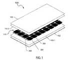
- FIG. 1shows an exploded view of an example solar cell module that may take advantage of embodiments of the present invention.
- FIG. 2schematically shows a cross-section of the solar cell module of FIG. 1 .
- FIGS. 3A and 3Bshow models for the mechanism the inventors believe causes solar cell polarization.
- FIGS. 4A , 4 B, 5 A, 5 B, 5 C, 5 D, and 6schematically show cross sections of solar cells in accordance with embodiments of the present invention.
- FIG. 7Aschematically shows a solar cell module in accordance with an embodiment of the present invention.
- FIGS. 7B and 7Cschematically show solar energy systems in accordance with embodiments of the present invention.
- FIG. 1there is shown an exploded view of an example solar cell module 100 that may take advantage of embodiments of the present invention.
- a solar cell moduleis also disclosed in commonly-assigned U.S. application Ser. No. 10/633,188, filed on Aug. 1, 2003. It is to be noted, however, that embodiments of the present invention are also applicable to other solar cell modules.
- the solar cell module 100includes a transparent cover 104 , encapsulants 103 (i.e., 103 - 1 , 103 - 2 ), a solar cell array 110 comprising interconnected solar cells 200 , and a back sheet 102 .
- the solar cell module 100is a so-called “terrestrial solar cell module” in that it is typically used in stationary applications, such as on rooftops or by power generating stations. As such, the solar cell module 100 is installed with the transparent cover 104 facing the sun.
- the transparent cover 104comprises glass.
- the front sides of the solar cells 200face towards the sun by way of the transparent cover 104 .
- Encapsulants 103crosslink and bond the solar cells 200 , the cover 104 , and the back sheet 102 to form a protective package.
- the encapsulants 103comprise poly-ethyl-vinyl acetate (“EVA”).
- the back sheet 102comprises Tedlar/Polyester/EVA (“TPE”) from the Madico company.
- TPETedlar/Polyester/EVA
- Tedlaris the outermost layer that protects against the environment
- the polyesterprovides additional electrical isolation
- the EVAis a non-crosslinked thin layer that promotes adhesion to the encapsulant 103 - 1 .
- Alternatives to TPE for use as the back sheet 102include Tedlar/Polyester/Tedlar (“TPT”), for example.
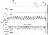
- FIG. 2schematically shows a cross-section of the solar cell module 100 .
- FIG. 2has been annotated with example materials for ease of understanding. However, it is to be noted that other materials may also be employed without detracting from the merits of the present invention.
- the front side of the solar cellcomprises materials, components, and features on the front side of the wafer 203 (i.e. from the passivation layer 202 towards the cover 104 ), while the backside of the solar cell comprises those on the backside of the wafer 203 (i.e. from the doped regions 204 towards the back sheet 102 ).
- the materials on the front side of the solar cell 200are configured to face the sun during normal operation.
- the materials on the front side of the solar cell 200are transparent by nature or thickness to allow solar radiation to shine through.
- a wafer 203comprises an n-type silicon wafer with an n-type front side diffusion region 207 .
- Front side diffusion region 207has been schematically separated with a dash line to indicate that it is in the silicon of wafer 203 .
- a dielectric passivation layer 202which comprises silicon dioxide in the example of FIG. 2 , is formed on the front side of the wafer 203 .
- An anti-reflective coating (“ARC”) 201is formed on top of the dielectric passivation layer 202 .
- the anti-reflective coating 201comprises silicon nitride formed to a thickness of about 400 Angstroms by plasma enhanced chemical vapor deposition (PECVD).
- the passivation layer 202comprises silicon dioxide formed to a thickness of about 200 Angstroms.
- the passivation layer 202may be grown directly on the top surface of the wafer 203 by high temperature oxidation.
- p-type doped (“P+”) and n-type doped (“N+”) regions 204 serving as charge collection junctions of the solar cell 200are formed in the wafer 203 .
- the p-type and n-type doped regions 204may also be formed external to the wafer 203 , such as in a layer formed on the backside of the wafer 203 , without detracting from the merits of the present invention.
- Metal contacts 206are formed on the backside of the solar cell 200 , with each metal contact 206 being coupled to a corresponding p-type doped or n-type doped collection region.
- An oxide layer 205is patterned to allow metal contacts 206 to be connected to the doped regions 204 .
- metal contacts 206are connected to metal contacts of other solar cells 200 in the solar cell array 110 .
- Metal contacts 206allow an external circuit or device to receive electrical current from the solar cell module 100 .
- the solar cell 200is a backside contact solar cell in that all electrical connections to its collection regions are formed on its backside.
- the solar cell 200is protected by back sheet 102 , encapsulants 103 , and cover 104 .
- a frame 211surrounds the solar cell 200 and its protection layers.
- the output power generation capability of the solar cell module 100may be substantially reduced. This reduction in output power is reversible in that the solar cell module 100 may be restored back to its original condition by, for example, biasing the solar cell module 100 with high voltage in a beneficial current flow direction. The inventors believe that this output power reduction is due to the solar cell 200 becoming polarized when charge leaks from the front side of the solar cell 200 to the frame 211 as indicated by arrow 212 .
- positive charge carriersleak from the front side of the solar cell 200 , thereby leaving the surface of the anti-reflective coating 201 negatively charged.
- the negative charge on the surface of the anti-reflective coating 201attracts positively charged light generated holes, some of which recombine with electrons in the n-type silicon wafer 203 instead of being collected at a doped collection region.
- harmful polarizationmay occur when, in the field, the dielectric passivation layer 202 has an electric field polarity such that electrons are repelled, and holes attracted, to the interface between the dielectric passivation layer 202 and front side diffusion region 207 , i.e., when the potential of the dielectric passivation layer 202 is less than the front side diffusion region 207 . In field operation, this would occur when the solar cell 200 is operated at a positive voltage with respect to ground. In other embodiments where a solar cell has a p-type front side diffusion region, harmful solar cell polarization may occur when the solar cell becomes negatively biased (i.e. becomes more negative) relative to ground in the field.
- a p-type silicon wafermay be doped to have an n-type front side diffusion region.
- an n-type silicon wafermay be doped to have a p-type front side diffusion region.
- the example solar cell 200has an n-type front side diffusion region in an n-type silicon wafer, the teachings of the present invention may be adapted to other types of solar cell substrates.
- FIG. 3Aschematically shows a model for the mechanism that the inventors believe is responsible for solar cell polarization.
- currentflows to or from the solar cell through the front of the glass (e.g. cover 104 ) and is leaked off by a shunt to the back surface of the solar cell.
- Resistance R glrepresents the leakage resistance from the nitride ARC (e.g. anti-reflective coating 201 ) to the glass front and R sh is the shunt leakage from the nitride ARC to the back of the solar cell.
- nitride ARCe.g. anti-reflective coating 201
- the nitride ARC to silicon wafer voltageshouldn't exceed the oxide breakdown voltage.
- the capacitance “C”represents a capacitor comprising an oxide passivation layer (e.g. dielectric passivation layer 202 ) serving as a dielectric, the nitride ARC serving as a first capacitor plate, and the silicon wafer serving as a second capacitor plate.
- FIG. 3Bschematically shows the lumped element approximation equivalent circuit for the structure of FIG. 3A .
- the voltagesare referenced to the back of the solar cell.
- the transient solution to this circuit, assuming that the starting gate voltage is zerois shown by equation EQ. 1.
- V G ⁇ ( t )V ⁇ R sh R sh + R gl ⁇ ( 1 - e - t / ⁇ ) EQ . ⁇ 1
- V Grepresents the voltage on the front EVA encapsulant, which behaves like a gate of a metal oxide semiconductor (MOS) transistor.
- MOSmetal oxide semiconductor
- the gate oxide of the MOS transistoris the oxide dielectric passivation layer.
- the capacitance “C”represents the capacitor formed by the nitride ARC, the oxide passivation layer, and the silicon wafer.
- the gatei.e. front side EVA encapsulant
- V Tvoltage
- t degdegradation time
- equation EQ. 2reduces to equation EQ. 3.
- V G ( t )V G (0) e ⁇ t/ ⁇ EQ. 4 If V T is the threshold where negligible degradation occurs, then the recovery time t rec is given by equation EQ. 5.
- Ultra violet rayswill have the effect of adding an additional shunt resistance in parallel with the existing one. This can be seen by assuming that the rate which ultra violet injects electrons from the nitride ARC to the silicon wafer is proportional to the trapped electron density. But the voltage across the capacitor “C” (see FIG. 3B ) is proportional to the trapped charge, therefore the current is proportional to the voltage on the gate capacitor; i.e., resistance-like. Assuming that this resistance is small compared to the other shunts (which it must be in order to have an effect) then the recovery time in the light t rec, light is given by equation EQ. 6.
- the conditions necessary for the ultra violet induced shunt to be sufficient to keep the solar cell module from degradingmay be calculated. This requires the condition given by EQ. 7 to be satisfied.
- harmful solar cell polarizationis prevented or minimized by increasing vertical electrical conductivity in the front side anti-reflective coating/passivation layer stack.
- chargeis bled from the front side of the solar cell to the bulk of the wafer.
- FIG. 4Aschematically shows a cross section of a solar cell 200 A in accordance with an embodiment of the present invention.
- the solar cell 200 Ais a specific embodiment of the solar cell 200 shown in FIG. 2 .
- the solar cell 200 Ais the same as the solar cell 200 except for the use of a very thin oxide (i.e. silicon dioxide) layer 202 A as a passivation layer 202 and an anti-reflective coating 201 A as an anti-reflective coating 201 .
- the anti-reflective coating 201 Amay comprise silicon carbide having a thickness of about 400 Angstroms and the wafer 203 comprises an N-type silicon wafer.
- the thin oxide layer 202 Ais preferably thin enough to bleed charge to the bulk of the wafer, to prevent charge buildup, and such that oxide breakdown occurs when it develops a relatively high voltage.
- the thin oxide layer 202 Amay be formed directly on the wafer 203 .
- the thin oxide layer 202 Ais formed to a thickness of about 10 Angstroms to 20 Angstroms using an ozone oxide process, which involves dipping the wafer 203 in a bath comprising ozone suspended in deionized water.
- FIG. 4Bschematically shows a cross section of a solar cell 200 B in accordance with an embodiment of the present invention.
- the solar cell 200 Bis a specific embodiment of the solar cell 200 shown in FIG. 2 .
- the solar cell 200 Bis the same as the solar cell 200 except for the use of a patterned dielectric passivation layer 202 B as a passivation level 202 .
- passivation layer 202 Bcomprises silicon dioxide
- the anti-reflective coating 201comprises silicon nitride
- the wafer 203comprises an N-type silicon wafer.
- the passivation layer 202 Bhas been patterned to have holes that allow a silicon nitride anti-reflective coating 201 to contact the silicon wafer 203 . This allows charge on the anti-reflective coating 201 to bleed to the bulk of the wafer 203 through the patterned holes in the oxide passivation layer 202 B.
- Each hole in passivation layer 202 Bmay be formed using a conventional lithography process, and be as small as the available lithography equipment allows.
- the patterned holesmay be separated by about 0.1 mm to about 2.0 mm from each other, for example.
- the perforated passivation layer 202 Badvantageously prevents solar cell polarization by preventing charge build up in the anti-reflective coating 201 .
- lateral conduction on the front side and towards the edges of the solar cellis increased to prevent solar cell polarization.
- passivation layershave natural defects (i.e. naturally formed holes) through them, it is possible for a conductive anti-reflective coating to bleed accumulated charge to the bulk of the wafer through the defects.
- some solar cell anti-reflective coatingsmay not be conductive enough for this to occur.
- a conductive layeris formed laterally to contact the anti-reflective coating to allow charge to bleed from the anti-reflective coating to the bulk of the wafer by way of the conductive layer and the natural defects in the passivation layer.
- the anti-reflective coatingitself is sufficiently conductive.
- FIG. 5Aschematically shows a cross section of a solar cell 200 C in accordance with an embodiment of the present invention.
- the solar cell 200 Cis a specific embodiment of the solar cell 200 shown in FIG. 2 .
- the solar cell 200 Cis the same as the solar cell 200 except that a transparent conductive coating 501 is formed on a top surface of the anti-reflective coating 201 .
- the passivation layer 202comprises silicon dioxide
- the anti-reflective coating 201comprises silicon nitride
- the wafer 203comprises an N-type silicon wafer.
- the transparent conductive coating 501comprises a conductive organic coating, such as the PEDOT/PSS (Baytron-P) coating.
- the transparent conductive coating 501may be sprayed or screen-printed directly on top of the anti-reflective coating 201 .
- the transparent conductive coating 501may be formed to a thickness of about 100 Angstroms, for example.
- the transparent conductive coating 501may be applied on the solar cell 200 as a last step in the solar cell fabrication process, just before encapsulation.
- the silicon nitride anti-reflective coating 201is not sufficiently conductive, charge in the silicon nitride can only travel a short distance, which is not enough to reach natural defects in the passivation layer 202 .
- the transparent conductive coating 501allows charge in the anti-reflective coating 201 to travel a distance sufficient to reach natural defects in the passivation layer 202 and bleed to the bulk of the wafer 203 .
- FIG. 5Bschematically shows a cross section of a solar cell 200 D in accordance with an embodiment of the present invention.
- the solar cell 200 Dis a specific embodiment of the solar cell 200 shown in FIG. 2 .
- the solar cell 200 Dis the same as the solar cell 200 except that a conductive anti-reflective coating (ARC) 201 B is used as an anti-reflective coating 201 .
- the passivation layer 202comprises silicon dioxide and the wafer 203 comprises an N-type silicon wafer.
- the conductive ARC 201 Badvantageously minimizes solar cell polarization by preventing charge from accumulating in it. Charge in the conductive ARC 201 B may bleed to the bulk of the wafer by way of natural defects in the passivation layer 202 .
- the conductive ARC 201 Bcomprises a naturally conductive (i.e. conductive without addition of impurities) anti-reflective coating, such as titanium oxide (TiO 2 ).
- the conductive ARC 201 Bcomprises a non-conductive anti-reflective material that is made conductive by addition of impurities.
- a non-conductive anti-reflective materialthat is made conductive by addition of impurities.
- the conductive ARC 201 Bmay comprise tin oxide doped with fluorine (SnO:F), zinc oxide doped with boron (ZnO:B), or silicon carbide doped with phosphorus (SiC:P) or boron (SiC:B).
- the conductive ARC 201 Bmay be formed to a thickness of about 400 Angstroms by plasma enhanced chemical vapor deposition (PECVD) of silicon carbide (SiC) with the addition of phosphine gas (PH 3 ) or diborane gas (B 2 H 6 ) during deposition.
- PECVDplasma enhanced chemical vapor deposition
- SiCsilicon carbide
- PH 3phosphine gas
- B 2 H 6diborane gas
- FIG. 5Cschematically shows a cross section of a solar cell 200 E in accordance with an embodiment of the present invention.
- the solar cell 200 Eis a specific embodiment of the solar cell 200 shown in FIG. 2 .
- the solar cell 200 Eis the same as the solar cell 200 except that a transparent conductive layer 502 is formed on top of the anti-reflective coating 201 .
- the passivation layer 202comprises silicon dioxide
- the anti-reflective coating 201comprises silicon nitride
- the silicon wafer 203comprises an N-type wafer.
- the transparent conductive layer 502allows charge in the anti-reflective coating 201 to travel a distance sufficient to reach natural defects in the passivation layer 202 and bleed to the bulk of the wafer 203 .
- Transparent conductive layer 502may be evaporated, sputtered, or deposited directly on top of the anti-reflective coating 201 .
- the transparent conductive layer 502may comprise a transparent conductive oxide, such as tin oxide doped with fluorine (SnO:F), zinc oxide doped with boron (ZnO:B), or silicon carbide doped with phosphorus (SiC:P) or boron (SiC:B) formed to a thickness of about 200 Angstroms.
- FIG. 5Dschematically shows a cross section of a solar cell 200 F in accordance with an embodiment of the present invention.
- the solar cell 200 Fis a specific embodiment of the solar cell 200 shown in FIG. 2 .
- the solar cell 200 Fis the same as the solar cell 200 except that a relatively thin (e.g. about 200 Angstroms) conductive layer 503 is formed between the passivation layer 202 and the anti-reflective coating 201 .
- the passivation layer 202comprises silicon dioxide
- the anti-reflective coating 201comprises silicon nitride
- the silicon wafer 203comprises an N-type wafer.
- the thin conductive layer 503allows charge to bleed from the anti-reflective coating 201 , to the thin conductive layer 503 , and to the bulk of the wafer 203 through natural defects in the passivation layer 202 .
- the conductive layer 503comprises polysilicon formed to a thickness of about 200 Angstroms directly on the top surface of the passivation layer 202 .
- the anti-reflective coating 201may be formed directly on a surface of the conductive layer 503 .
- the conductive layer 503may be formed by PECVD and in-situ (i.e. in the same chamber or cluster tool in one loading) with the formation of the anti-reflective coating 201 .
- the conductive layer 503may also comprise tin oxide doped with fluorine (SnO:F), zinc oxide doped with boron (ZnO:B), or silicon carbide doped with phosphorus (SiC:P) or boron (SiC:B) formed to a thickness of about 200 Angstroms.
- conductivity from the front side of the solar cell to the bulk of the waferis increased to prevent harmful solar cell polarization. This is equivalent to lowering the shunt resistance R sh in the model of FIG. 3B .
- the resistance from the front side of the solar cell to the rest of the module by way of the transparent coveris increased to prevent charge leakage. This is equivalent to increasing the resistance R gl in the model of FIG. 3B .
- Resistance from the front side of the solar cell to the rest of the solar cell modulemay be increased by blocking the charge leakage path, as now described with reference to FIG. 6 .
- FIG. 6schematically shows a cross section of a solar cell 200 G in accordance with an embodiment of the present invention.
- the solar cell 200 Gis a specific embodiment of the solar cell 200 shown in FIG. 2 .
- the solar cell 200 Gis the same as the solar cell 200 except that a transparent electrical insulator layer 691 is formed over the anti-reflective coating 201 .
- the passivation layer 202comprises silicon dioxide
- the anti-reflective coating 201comprises silicon nitride
- the silicon wafer 203comprises an N-type wafer.
- the electrical insulator layer 691is formed over the anti-reflective coating 201 to prevent solar cell polarization by preventing charge from leaking out from the front side of the solar cell 200 G towards the cover 104 (see FIG. 2 ).
- the electrical insulator layer 691comprises silicon dioxide (SiO 2 ) formed to a thickness of about 0.1 to 1.0 ⁇ m by atmospheric pressure chemical vapor deposition (APCVD).
- Harmful solar cell polarizationmay also be prevented by biasing a region of a solar cell module on the front side of the solar cell, as now discussed with reference to FIG. 7A .
- FIG. 7Aschematically shows a solar cell module 100 A in accordance with an embodiment of the present invention.
- the solar cell module 100 Ais a specific embodiment of the solar cell module 100 shown in FIG. 2 .
- Several solar cells 200along with their interconnects 200 , are shown in FIG. 7A .
- An interconnect 682serially connects one solar cell 200 to another.
- the solar cell module 100 Ais essentially the same as the solar cell module 100 except that an electrically conductive path is added to bring up the potential of the part of the module in front of the cell to prevent harmful leakage current (i.e., above, at, or within 30V for n-type cell modules).
- the conductive pathis formed by placing a transparent electrically conductive layer 684 on the back surface of the transparent cover 104 (e.g. glass) and connecting the conductive layer 684 to the back surface of a solar cell 200 .
- the conductive layer 684is electrically connected to an interconnect 682 , which is connected to the backside of a solar cell 200 by way of an electrical connection 683 .
- the preferred embodimentis for the conductive layer 684 to be connected to the interconnect 682 that is connected to the highest (i.e.
- the conductive layer 684is isolated from the frame of the solar cell module 100 A to prevent an unsafe condition where a high-voltage is on the exterior of the module.
- the conductive layer 684may comprise tin oxide doped with fluorine (SnO:F), indium tin oxide (ITO), zinc oxide (ZnO), or other transparent oxides or transparent organic conductors. In the preferred embodiment, this conductive layer has a sheet resistance of approximately 5e4 ohm/square.
- the back sheet 102is formed on the bottom surface of the encapsulant 103 as before.
- the encapsulant 103is made electrically conductive to form a near-equipotential field above the solar cells 200 ; the encapsulant at the edges of the module remains electrically insulating to prevent an unsafe condition where a high-voltage is on the exterior of the module.
- the entire solar energy systemis taken into consideration to prevent charge from leaking from the front side of the solar cell.
- an array of solar cell modulesmay be biased such that leaking of charge carriers from the front side of the solar cells is prevented.
- Example system level approaches to the solar cell polarization problemare now described with reference to FIGS. 7B and 7C .
- FIG. 7Bschematically illustrates a solar energy system 790 in accordance with an embodiment of the present invention.
- a solar cell module array 630has several solar cell modules comprising inter-connected solar cells 200 .
- the positive output terminal of the solar cell module array 630is labeled as node 616
- its negative output terminalis labeled as node 617 .
- the solar cells 200are series connected such that their positive terminals are toward the node 616 and their negative terminals are toward the node 617 .
- the solar cell module array 630is coupled to an inverter 600 .
- An inverterconverts direct current (DC) to alternating current (AC).
- the inverter 600receives direct current from the solar cell module array 630 and outputs alternating current to a power grid.
- a DC to DC converter 601converts direct current from the solar cell module array 630 to another direct current.
- the direct current output of the DC to DC converter 601is converted to alternating current by DC to AC converter 602 .
- the alternating current output of the DC to AC converter 602is provided to the power grid by way of an isolation circuit 603 .
- the isolation circuit 603may be in series between the DC to DC converter 601 and the DC to AC converter 602 .
- the positive terminal of the solar cell array module 630is grounded. Systems similar to the solar energy system 790 may be used in North America and Japan among other countries.
- the frame 614which represents the frame of all solar cell modules in the solar cell module array 630 is also grounded as indicated by the label 611 . Grounding the positive terminal of the solar cell module array 630 and the frame 614 reduces the potential between the solar cells 200 and the frame 614 , minimizing leakage from the front side of the solar cells 200 .
- the positive terminal of the solar cell module array 630may be tied to ground within or outside of the inverter 600 .
- each solar cell 200has an n-type front side diffusion region.
- harmful solar cell polarizationoccurs because the solar cells 200 become positively biased relative to ground.
- the highest or near highest potential of the solar cell module array 630(node 616 in this case) is accordingly tied to ground.
- harmful polarizationmay occur when the solar cells become negatively biased relative to ground.
- the lowest or near lowest potential solar cell in the arraye.g. the negative output terminal of the solar cell module array
- FIG. 7Cschematically illustrates a solar energy system 795 in accordance with an embodiment of the present invention.
- the solar cell module array 630has several solar cell modules comprising several inter-connected solar cells 200 .
- the positive output terminal of the solar cell module array 630is labeled as node 616
- its negative output terminalis labeled as node 617 .
- the solar cells 200are series connected such that their positive terminals are toward the node 616 and their negative terminals are toward the node 617 .
- the solar cell module array 630is coupled to an inverter 650 .
- the inverter 650receives direct current from the solar cell module array 630 and outputs alternating current to the power grid.
- a DC to DC converter 651converts direct current from the solar cell module array 630 to another direct current.
- the direct current output of the DC to DC converter 651is coupled to a DC to AC converter 652 by an isolation circuit 653 .
- the alternating current output of the DC to AC converter 652is provided to the power grid.
- the isolation circuit 653may be located at the output of the DC to AC converter 652 to provide AC output to the power grid.
- Systems similar to the solar energy system 795may be employed in countries covered by IEC regulations, such as most European countries, the United Kingdom, and others.
- the output of the solar cell array module 630is balanced to +/ ⁇ 1 ⁇ 2 (i.e. plus/minus half) the value of the total voltage of the solar cell module array 630 . That is, the voltage at node 616 is ideally +1 ⁇ 2 of the total voltage of the solar cell module array 630 , while the voltage at node 617 is ideally ⁇ 1 ⁇ 2 of the total voltage of the solar cell array module 630 .
- the resistors 672 and 673are high value resistors (or varistors) that balance the output of the solar cell module array 630 at around the ground point. In practice, the output of the solar cell module array 630 is only approximately balanced because the balancing resistors 672 and 673 have high resistance (e.g. about 10 M ⁇ each).
- the solar cell module array 630would be floating because there would be no resistor 671 and the inverter 650 has DC-DC isolation between the output of the solar cell module array 630 and the AC output to the power grid.
- the inventorsdiscovered, however, that such an installation will cause harmful polarization of solar cells 200 .
- the positive terminal of the solar cell module array 630is connected to ground by way of a resistor 671 .
- the resistor 671may be a fixed, variable, or electronically controlled resistance without detracting from the merits of the present invention.
- the resistor 671biases the solar cell module array 630 closer to the positive side of its output to prevent positive charge from leaking from the front sides of the solar cells 200 .
- the resistor 671“unbalances” the output of the solar cell module array 630 towards positive to prevent solar cell polarization.
- node 617(instead of node 616 ) may be connected to ground by way of the resistor 671 to bias the solar cell module array 630 towards its negative output.
- the resistor 671may have a resistance of about ⁇ 1/10 th of the value of a balancing resistor (i.e. resistor 672 or 673 ).
- inverter 650may also be configured such that it unbalances the balanced output of the solar cell module array 630 towards positive or negative, depending on the polarity of the leaking charge carrier (i.e. electrons or holes). For example, the value of resistor 672 may be increased relative to resistor 673 to unbalance the output of the solar cell module array 630 without using the resistor 671 .
- the resistor 671may also comprise an electronically controlled resistance.
- the resistance of the resistor 671may be controlled by an electronic circuit by switching in different resistance values depending on condition.
- Such an electronic circuitmay have sensors that detect when a lower resistance is needed when the solar cell module array resistance is reduced to ground level, such as when raining, for example.
- each solar cell 200has an n-type front side diffusion region.
- harmful solar cell polarizationoccurs because the solar cells 200 become positively biased relative to ground.
- the highest or near highest potential of the solar cell module array 630(node 616 in this case) is accordingly tied to ground by way of a resistance (e.g. resistor 671 ).
- harmful polarizationmay occur when the solar cells become negatively biased relative to ground.
- the lowest or near lowest potential solar cell in the arraye.g. the negative output terminal of the solar cell module array
Landscapes
- Engineering & Computer Science (AREA)
- Power Engineering (AREA)
- Photovoltaic Devices (AREA)
- Life Sciences & Earth Sciences (AREA)
- Sustainable Development (AREA)
- Manufacturing & Machinery (AREA)
- Sustainable Energy (AREA)
- Inverter Devices (AREA)
Abstract
Description
Where
and Reqis the parallel equivalent resistance. VGrepresents the voltage on the front EVA encapsulant, which behaves like a gate of a metal oxide semiconductor (MOS) transistor. The gate oxide of the MOS transistor is the oxide dielectric passivation layer. As mentioned, the capacitance “C” represents the capacitor formed by the nitride ARC, the oxide passivation layer, and the silicon wafer.
equation EQ. 2 reduces to equation EQ. 3.
From equation EQ. 3, it can be readily seen that for high voltages, the time to a specific amount of degradation is inversely proportional to the applied voltage.
VG(t)=VG(0)e−t/τ EQ. 4
If VTis the threshold where negligible degradation occurs, then the recovery time trecis given by equation EQ. 5.
The above equations can be rearranged to show that EQ. 7 is satisfied when the recovery time in the light is given by equation EQ. 8.
In other words, if the module solar cell module recovers in sunlight, when unbiased, in a shorter time than it takes to degrade in the dark with an applied bias, then the module will be stable in sunlight with that applied bias.
Claims (10)
Priority Applications (19)
| Application Number | Priority Date | Filing Date | Title |
|---|---|---|---|
| US11/210,213US7554031B2 (en) | 2005-03-03 | 2005-08-22 | Preventing harmful polarization of solar cells |
| KR1020097007569AKR101080583B1 (en) | 2005-03-03 | 2006-01-20 | Preventing harmful polarization of solar cells |
| EP06719101.5AEP1854147B1 (en) | 2005-03-03 | 2006-01-20 | Preventing harmful polarization of solar cells |
| KR1020077019044AKR100933598B1 (en) | 2005-03-03 | 2006-01-20 | Prevention of harmful polarization of solar cells |
| CN201210443834.0ACN102945864B (en) | 2005-03-03 | 2006-01-20 | Preventing harmful polarization of solar cells |
| PCT/US2006/002137WO2006096247A2 (en) | 2005-03-03 | 2006-01-20 | Preventing harmful polarization of solar cells |
| CN2011101170449ACN102194911B (en) | 2005-03-03 | 2006-01-20 | Preventing harmful polarization of solar cells |
| CN2006800068188ACN101133500B (en) | 2005-03-03 | 2006-01-20 | Prevents harmful solar cell polarization |
| JP2007558005AJP5224444B2 (en) | 2005-03-03 | 2006-01-20 | Prevention of harmful polarization in solar cells |
| CN201210112491.XACN102683442B (en) | 2005-03-03 | 2006-01-20 | Preventing harmful polarization of solar cells |
| US12/477,796US7786375B2 (en) | 2005-03-03 | 2009-06-03 | Preventing harmful polarization of solar cells |
| US12/845,627US9035167B2 (en) | 2005-03-03 | 2010-07-28 | Preventing harmful polarization of solar cells |
| JP2010291035AJP5570411B2 (en) | 2005-03-03 | 2010-12-27 | Prevention of harmful polarization in solar cells |
| JP2011243477AJP5439459B2 (en) | 2005-03-03 | 2011-11-07 | Prevention of harmful polarization in solar cells |
| JP2014069285AJP5806358B2 (en) | 2005-03-03 | 2014-03-28 | Prevention of harmful polarization in solar cells |
| US14/687,624US20150288328A1 (en) | 2005-03-03 | 2015-04-15 | Preventing harmful polarization of solar cells |
| US15/230,182US10164567B2 (en) | 2005-03-03 | 2016-08-05 | Preventing harmful polarization of solar cells |
| US15/240,913US9774294B2 (en) | 2005-03-03 | 2016-08-18 | Preventing harmful polarization of solar cells |
| US16/196,340US10903786B2 (en) | 2005-03-03 | 2018-11-20 | Preventing harmful polarization of solar cells |
Applications Claiming Priority (2)
| Application Number | Priority Date | Filing Date | Title |
|---|---|---|---|
| US65870605P | 2005-03-03 | 2005-03-03 | |
| US11/210,213US7554031B2 (en) | 2005-03-03 | 2005-08-22 | Preventing harmful polarization of solar cells |
Related Child Applications (1)
| Application Number | Title | Priority Date | Filing Date |
|---|---|---|---|
| US12/477,796ContinuationUS7786375B2 (en) | 2005-03-03 | 2009-06-03 | Preventing harmful polarization of solar cells |
Publications (2)
| Publication Number | Publication Date |
|---|---|
| US20060196535A1 US20060196535A1 (en) | 2006-09-07 |
| US7554031B2true US7554031B2 (en) | 2009-06-30 |
Family
ID=36942960
Family Applications (7)
| Application Number | Title | Priority Date | Filing Date |
|---|---|---|---|
| US11/210,213Active2026-12-31US7554031B2 (en) | 2005-03-03 | 2005-08-22 | Preventing harmful polarization of solar cells |
| US12/477,796Expired - LifetimeUS7786375B2 (en) | 2005-03-03 | 2009-06-03 | Preventing harmful polarization of solar cells |
| US12/845,627Active2026-07-17US9035167B2 (en) | 2005-03-03 | 2010-07-28 | Preventing harmful polarization of solar cells |
| US14/687,624AbandonedUS20150288328A1 (en) | 2005-03-03 | 2015-04-15 | Preventing harmful polarization of solar cells |
| US15/230,182Active2025-11-05US10164567B2 (en) | 2005-03-03 | 2016-08-05 | Preventing harmful polarization of solar cells |
| US15/240,913Expired - LifetimeUS9774294B2 (en) | 2005-03-03 | 2016-08-18 | Preventing harmful polarization of solar cells |
| US16/196,340Expired - LifetimeUS10903786B2 (en) | 2005-03-03 | 2018-11-20 | Preventing harmful polarization of solar cells |
Family Applications After (6)
| Application Number | Title | Priority Date | Filing Date |
|---|---|---|---|
| US12/477,796Expired - LifetimeUS7786375B2 (en) | 2005-03-03 | 2009-06-03 | Preventing harmful polarization of solar cells |
| US12/845,627Active2026-07-17US9035167B2 (en) | 2005-03-03 | 2010-07-28 | Preventing harmful polarization of solar cells |
| US14/687,624AbandonedUS20150288328A1 (en) | 2005-03-03 | 2015-04-15 | Preventing harmful polarization of solar cells |
| US15/230,182Active2025-11-05US10164567B2 (en) | 2005-03-03 | 2016-08-05 | Preventing harmful polarization of solar cells |
| US15/240,913Expired - LifetimeUS9774294B2 (en) | 2005-03-03 | 2016-08-18 | Preventing harmful polarization of solar cells |
| US16/196,340Expired - LifetimeUS10903786B2 (en) | 2005-03-03 | 2018-11-20 | Preventing harmful polarization of solar cells |
Country Status (6)
| Country | Link |
|---|---|
| US (7) | US7554031B2 (en) |
| EP (1) | EP1854147B1 (en) |
| JP (4) | JP5224444B2 (en) |
| KR (2) | KR100933598B1 (en) |
| CN (4) | CN102683442B (en) |
| WO (1) | WO2006096247A2 (en) |
Cited By (54)
| Publication number | Priority date | Publication date | Assignee | Title |
|---|---|---|---|---|
| US20080202576A1 (en)* | 2007-02-16 | 2008-08-28 | Henry Hieslmair | Solar cell structures, photovoltaic panels and corresponding processes |
| US20090078304A1 (en)* | 2007-09-26 | 2009-03-26 | Jack Arthur Gilmore | Photovoltaic charge abatement device, system, and method |
| US20090260673A1 (en)* | 2005-03-03 | 2009-10-22 | Swanson Richard M | Preventing Harmful Polarization Of Solar Cells |
| US20090283130A1 (en)* | 2007-08-03 | 2009-11-19 | Advanced Energy Industries, Inc. | System, method, and apparatus for remotely coupling photovoltaic arrays |
| US20100139743A1 (en)* | 2009-07-30 | 2010-06-10 | Tigo Energy | Novel System and Method for Addressing Solar Energy Production Capacity Loss Due to Field Buildup Between Cells and Glass and Frame Assembly |
| US20100139740A1 (en)* | 2009-08-07 | 2010-06-10 | Grace Xavier | Module Level Solutions to Solar Cell Polarization |
| US20100294349A1 (en)* | 2009-05-20 | 2010-11-25 | Uma Srinivasan | Back contact solar cells with effective and efficient designs and corresponding patterning processes |
| US20110012264A1 (en)* | 2009-07-20 | 2011-01-20 | Ryan Linderman | Optoelectronic device with heat spreader unit |
| US20110030778A1 (en)* | 2009-08-06 | 2011-02-10 | Energy Focus, Inc. | Method of Passivating and Reducing Reflectance of a Photovoltaic Cell |
| WO2011025575A1 (en) | 2009-08-27 | 2011-03-03 | Sunpower Corporation | Module level solution to solar cell polarization using an encapsulant with opened uv transmission curve |
| DE102009044052A1 (en)* | 2009-09-18 | 2011-03-24 | Schott Solar Ag | Crystalline solar cell, process for producing the same and process for producing a solar cell module |
| US20110094575A1 (en)* | 2009-10-27 | 2011-04-28 | Calisolar Inc. | Polarization Resistant Solar Cell Design Using an Oxygen-Rich Interface Layer |
| US20110120524A1 (en)* | 2009-11-20 | 2011-05-26 | Sunpower Corporation | Device and method for solar power generation |
| US20110132431A1 (en)* | 2009-12-08 | 2011-06-09 | Ryan Linderman | Optoelectronic device with bypass diode |
| US20110240105A1 (en)* | 2010-03-30 | 2011-10-06 | Andy Luan | Leakage pathway layer for solar cell |
| US20120070934A1 (en)* | 2010-03-19 | 2012-03-22 | Hirak Mitra | Method to build transparent polarizing solar cell |
| US20120211081A1 (en)* | 2011-02-21 | 2012-08-23 | Semiconductor Energy Laboratory Co., Ltd. | Photoelectric conversion device |
| WO2012145228A1 (en) | 2011-04-20 | 2012-10-26 | Sunpower Corporation | Solar cell module structure and fabrication method for preventing polarization |
| US8336539B2 (en) | 2010-08-03 | 2012-12-25 | Sunpower Corporation | Opposing row linear concentrator architecture |
| US8377738B2 (en) | 2010-07-01 | 2013-02-19 | Sunpower Corporation | Fabrication of solar cells with counter doping prevention |
| DE102011081863A1 (en) | 2011-08-31 | 2013-02-28 | Robert Bosch Gmbh | Solar cell and process for its production |
| US20130081668A1 (en)* | 2011-09-30 | 2013-04-04 | Ryan J. Linderman | Thermal tracking for solar systems |
| US8528366B2 (en) | 2011-12-22 | 2013-09-10 | Sunpower Corporation | Heat-regulating glass bending apparatus and method |
| US8563849B2 (en) | 2010-08-03 | 2013-10-22 | Sunpower Corporation | Diode and heat spreader for solar module |
| US8604404B1 (en) | 2010-07-01 | 2013-12-10 | Sunpower Corporation | Thermal tracking for solar systems |
| US8636198B1 (en) | 2012-09-28 | 2014-01-28 | Sunpower Corporation | Methods and structures for forming and improving solder joint thickness and planarity control features for solar cells |
| US8796061B2 (en) | 2012-12-21 | 2014-08-05 | Sunpower Corporation | Module assembly for thin solar cells |
| US8839784B2 (en) | 2010-12-22 | 2014-09-23 | Sunpower Corporation | Locating connectors and methods for mounting solar hardware |
| US8893713B2 (en) | 2010-12-22 | 2014-11-25 | Sunpower Corporation | Locating connectors and methods for mounting solar hardware |
| US8912083B2 (en) | 2011-01-31 | 2014-12-16 | Nanogram Corporation | Silicon substrates with doped surface contacts formed from doped silicon inks and corresponding processes |
| US9035168B2 (en) | 2011-12-21 | 2015-05-19 | Sunpower Corporation | Support for solar energy collectors |
| US9035172B2 (en) | 2012-11-26 | 2015-05-19 | Sunpower Corporation | Crack resistant solar cell modules |
| US9038421B2 (en) | 2011-07-01 | 2015-05-26 | Sunpower Corporation | Glass-bending apparatus and method |
| WO2015171575A1 (en) | 2014-05-09 | 2015-11-12 | E. I. Du Pont De Nemours And Company | Encapsulant composition comprising a copolymer of ethylene, vinyl acetate and a third comonomer |
| US9246037B2 (en) | 2010-12-03 | 2016-01-26 | Sunpower Corporation | Folded fin heat sink |
| US9397611B2 (en) | 2012-03-27 | 2016-07-19 | Sunpower Corporation | Photovoltaic systems with local maximum power point tracking prevention and methods for operating same |
| US9685571B2 (en) | 2013-08-14 | 2017-06-20 | Sunpower Corporation | Solar cell module with high electric susceptibility layer |
| US9812590B2 (en) | 2012-10-25 | 2017-11-07 | Sunpower Corporation | Bifacial solar cell module with backside reflector |
| US9897346B2 (en) | 2010-08-03 | 2018-02-20 | Sunpower Corporation | Opposing row linear concentrator architecture |
| US9911882B2 (en) | 2010-06-24 | 2018-03-06 | Sunpower Corporation | Passive flow accelerator |
| US20180097133A1 (en)* | 2015-07-27 | 2018-04-05 | Sierra Nevada Corporation | Solar array system and method of manufacturing |
| USD822890S1 (en) | 2016-09-07 | 2018-07-10 | Felxtronics Ap, Llc | Lighting apparatus |
| USD832495S1 (en) | 2017-08-18 | 2018-10-30 | Flex Ltd. | Lighting module locking mechanism |
| USD832494S1 (en) | 2017-08-09 | 2018-10-30 | Flex Ltd. | Lighting module heatsink |
| USD833061S1 (en) | 2017-08-09 | 2018-11-06 | Flex Ltd. | Lighting module locking endcap |
| USD846793S1 (en) | 2017-08-09 | 2019-04-23 | Flex Ltd. | Lighting module locking mechanism |
| WO2019173262A1 (en) | 2018-03-08 | 2019-09-12 | E. I. Du Pont De Nemours And Company | Photovoltaic module and encapsulant composition having improved resistance to potential induced degradation |
| USD862777S1 (en) | 2017-08-09 | 2019-10-08 | Flex Ltd. | Lighting module wide distribution lens |
| USD862778S1 (en) | 2017-08-22 | 2019-10-08 | Flex Ltd | Lighting module lens |
| USD872319S1 (en) | 2017-08-09 | 2020-01-07 | Flex Ltd. | Lighting module LED light board |
| USD877964S1 (en) | 2017-08-09 | 2020-03-10 | Flex Ltd. | Lighting module |
| USD888323S1 (en) | 2017-09-07 | 2020-06-23 | Flex Ltd | Lighting module wire guard |
| WO2020126614A1 (en) | 2018-12-20 | 2020-06-25 | Forschungszentrum Jülich GmbH | Method and device for reducing the potentially induced degradation of solar cells |
| US10775030B2 (en) | 2017-05-05 | 2020-09-15 | Flex Ltd. | Light fixture device including rotatable light modules |
Families Citing this family (98)
| Publication number | Priority date | Publication date | Assignee | Title |
|---|---|---|---|---|
| EP1947721A4 (en)* | 2005-09-29 | 2013-08-07 | Micro Silitron Inc | FUEL BATTERY CELL, FUEL BATTERY BATTERY NETWORK, FUEL BATTERY MODULE, AND FUEL BATTERY SYSTEM |
| GB2442254A (en)* | 2006-09-29 | 2008-04-02 | Renewable Energy Corp Asa | Back contacted solar cell |
| US20080135088A1 (en)* | 2006-12-11 | 2008-06-12 | Sunmodular, Inc. | Interlocking solar roof tiles with heat exchange |
| US8410350B2 (en)* | 2006-12-11 | 2013-04-02 | Ns Acquisition Llc | Modular solar panels with heat exchange |
| US7728219B2 (en)* | 2006-12-11 | 2010-06-01 | Sunmodular, Inc. | Photovoltaic cells, modules and methods of making same |
| AU2007346834A1 (en)* | 2007-02-08 | 2008-08-21 | Wuxi Suntech-Power Co., Ltd. | Hybrid silicon solar cells and method of fabricating same |
| US7670638B2 (en)* | 2007-05-17 | 2010-03-02 | Sunpower Corporation | Protection layer for fabricating a solar cell |
| US7838062B2 (en)* | 2007-05-29 | 2010-11-23 | Sunpower Corporation | Array of small contacts for solar cell fabrication |
| US20090217964A1 (en)* | 2007-09-26 | 2009-09-03 | Advanced Energy Industries, Inc. | Device, system, and method for improving the efficiency of solar panels |
| US8987039B2 (en) | 2007-10-12 | 2015-03-24 | Air Products And Chemicals, Inc. | Antireflective coatings for photovoltaic applications |
| DE102007054384A1 (en) | 2007-11-14 | 2009-05-20 | Institut Für Solarenergieforschung Gmbh | Method for producing a solar cell with a surface-passivating dielectric double layer and corresponding solar cell |
| US8198528B2 (en)* | 2007-12-14 | 2012-06-12 | Sunpower Corporation | Anti-reflective coating with high optical absorption layer for backside contact solar cells |
| KR20090067350A (en)* | 2007-12-21 | 2009-06-25 | 주성엔지니어링(주) | Thin film type solar cell and manufacturing method thereof |
| WO2009098241A1 (en)* | 2008-02-05 | 2009-08-13 | Oerlikon Trading Ag, Trübbach | Encapsulation of optoelectronic devices |
| US8440903B1 (en)* | 2008-02-21 | 2013-05-14 | Stion Corporation | Method and structure for forming module using a powder coating and thermal treatment process |
| US8076175B2 (en)* | 2008-02-25 | 2011-12-13 | Suniva, Inc. | Method for making solar cell having crystalline silicon P-N homojunction and amorphous silicon heterojunctions for surface passivation |
| US20090211623A1 (en)* | 2008-02-25 | 2009-08-27 | Suniva, Inc. | Solar module with solar cell having crystalline silicon p-n homojunction and amorphous silicon heterojunctions for surface passivation |
| US20090211627A1 (en)* | 2008-02-25 | 2009-08-27 | Suniva, Inc. | Solar cell having crystalline silicon p-n homojunction and amorphous silicon heterojunctions for surface passivation |
| US8481357B2 (en)* | 2008-03-08 | 2013-07-09 | Crystal Solar Incorporated | Thin film solar cell with ceramic handling layer |
| US20110198304A1 (en)* | 2008-05-01 | 2011-08-18 | Linus Eric Wallgren | Rack Assembly for Solar Energy Collecting Module |
| US20090277503A1 (en)* | 2008-05-10 | 2009-11-12 | Solfocus, Inc. | Solar Cell with Current Blocking Layer |
| US7851698B2 (en)* | 2008-06-12 | 2010-12-14 | Sunpower Corporation | Trench process and structure for backside contact solar cells with polysilicon doped regions |
| US8049097B2 (en)* | 2008-08-11 | 2011-11-01 | General Electric Company | Solar cell including cooling channels and method for fabrication |
| CN102165604A (en)* | 2008-09-29 | 2011-08-24 | 薄膜硅公司 | Monolithic Integrated Solar Modules |
| US20100108130A1 (en)* | 2008-10-31 | 2010-05-06 | Crystal Solar, Inc. | Thin Interdigitated backside contact solar cell and manufacturing process thereof |
| US20100108134A1 (en)* | 2008-10-31 | 2010-05-06 | Crystal Solar, Inc. | Thin two sided single crystal solar cell and manufacturing process thereof |
| EP2347958B1 (en)* | 2008-11-12 | 2018-09-05 | Kyushu Institute of Technology | Device for suppressing sustained discharge on solar battery array |
| JP5123830B2 (en)* | 2008-11-26 | 2013-01-23 | ルネサスエレクトロニクス株式会社 | Antireflection film, method for manufacturing antireflection film, and semiconductor device using antireflection film |
| FR2939240B1 (en)* | 2008-12-03 | 2011-02-18 | Saint Gobain | LAYERED ELEMENT AND PHOTOVOLTAIC DEVICE COMPRISING SUCH A MEMBER |
| CN105304728B (en)* | 2009-02-11 | 2019-01-04 | 新南创新私人有限公司 | Photovoltaic device structure and method |
| DE102009003467A1 (en)* | 2009-02-11 | 2010-08-19 | Q-Cells Se | Rear-contacted solar cell |
| US8258395B2 (en)* | 2009-02-24 | 2012-09-04 | Sunpower Corporation | Photovoltaic module and interlocked stack of photovoltaic modules |
| CN101817245B (en)* | 2009-02-27 | 2013-06-26 | E.I.内穆尔杜邦公司 | Solar cell pack |
| JP5377018B2 (en)* | 2009-03-23 | 2013-12-25 | 株式会社東芝 | Solar power system |
| US20120042952A1 (en)* | 2009-04-30 | 2012-02-23 | Industry-University Cooperation Foundation Hanyang University | Silicon solar cell comprising a carbon nanotube layer |
| DE202009018068U1 (en) | 2009-06-02 | 2010-12-23 | Solon Se | solar module |
| US20100313952A1 (en)* | 2009-06-10 | 2010-12-16 | Thinsilicion Corporation | Photovoltaic modules and methods of manufacturing photovoltaic modules having multiple semiconductor layer stacks |
| KR101154727B1 (en)* | 2009-06-30 | 2012-06-08 | 엘지이노텍 주식회사 | Solar cell and method of fabricating the same |
| DE102009031982A1 (en)* | 2009-07-06 | 2011-01-13 | Schott Solar Ag | Photovoltaic module and photovoltaic device |
| US20110041910A1 (en)* | 2009-08-18 | 2011-02-24 | Semiconductor Energy Laboratory Co., Ltd. | Photoelectric conversion device and manufacturing method thereof |
| US8614903B2 (en)* | 2009-08-24 | 2013-12-24 | Mitsubishi Electric Corporation | Power conditioner for photovoltaic power generation |
| DE202010018510U1 (en)* | 2009-09-07 | 2017-03-15 | Lg Electronics Inc. | solar cell |
| CN102044579B (en) | 2009-09-07 | 2013-12-18 | Lg电子株式会社 | Solar cell |
| US20110056532A1 (en)* | 2009-09-09 | 2011-03-10 | Crystal Solar, Inc. | Method for manufacturing thin crystalline solar cells pre-assembled on a panel |
| DE102009044142A1 (en) | 2009-09-30 | 2011-03-31 | Saint-Gobain Sekurit Deutschland Gmbh & Co. Kg | Thin-film component on glass, a process for its production and its use |
| TW201140866A (en) | 2009-12-07 | 2011-11-16 | Applied Materials Inc | Method of cleaning and forming a negatively charged passivation layer over a doped region |
| FR2955702B1 (en)* | 2010-01-27 | 2012-01-27 | Commissariat Energie Atomique | PHOTOVOLTAIC CELL COMPRISING A THIN SILICON CRYSTALLINE OXIDE PASSIVATION FILM AND METHOD OF MAKING SAME |
| JP5215330B2 (en)* | 2010-02-01 | 2013-06-19 | シャープ株式会社 | Manufacturing method of back electrode type solar cell, back electrode type solar cell and back electrode type solar cell module |
| JP2013524510A (en)* | 2010-03-30 | 2013-06-17 | アプライド マテリアルズ インコーポレイテッド | Method for forming a negatively charged passivation layer on a p-type diffusion layer |
| JP5213188B2 (en)* | 2010-04-27 | 2013-06-19 | シャープ株式会社 | Back electrode type solar cell and method of manufacturing back electrode type solar cell |
| US8211731B2 (en) | 2010-06-07 | 2012-07-03 | Sunpower Corporation | Ablation of film stacks in solar cell fabrication processes |
| DE102010023262A1 (en)* | 2010-06-09 | 2011-12-15 | Danfoss Solar Inverters A/S | Solar power plant with increased service life |
| DE102010017461B4 (en)* | 2010-06-18 | 2013-11-14 | Hanwha Q.CELLS GmbH | Solar cell, solar cell manufacturing process and test method |
| US8263899B2 (en) | 2010-07-01 | 2012-09-11 | Sunpower Corporation | High throughput solar cell ablation system |
| US20120048372A1 (en)* | 2010-08-25 | 2012-03-01 | Hyungseok Kim | Solar cell |
| KR101275575B1 (en)* | 2010-10-11 | 2013-06-14 | 엘지전자 주식회사 | Back contact solar cell and manufacturing method thereof |
| DE102010060463B4 (en)* | 2010-11-09 | 2013-04-25 | Sma Solar Technology Ag | Circuit arrangement for potential adjustment of a photovoltaic generator and photovoltaic system |
| US9337361B2 (en)* | 2010-11-26 | 2016-05-10 | Semiconductor Energy Laboratory Co., Ltd. | Photoelectric conversion device and manufacturing method thereof |
| JP5723143B2 (en)* | 2010-12-06 | 2015-05-27 | シャープ株式会社 | Manufacturing method of back electrode type solar cell and back electrode type solar cell |
| US8586403B2 (en) | 2011-02-15 | 2013-11-19 | Sunpower Corporation | Process and structures for fabrication of solar cells with laser ablation steps to form contact holes |
| JP2012182275A (en)* | 2011-03-01 | 2012-09-20 | Sharp Corp | Solar cell and method for manufacturing solar cell |
| US8726897B2 (en) | 2011-03-15 | 2014-05-20 | Sunedison, Llc | Collapsible solar module support system and method for assembling the same |
| US8872018B1 (en)* | 2011-05-06 | 2014-10-28 | The Boeing Company | Atomic oxygen and electrostatic-resistant, flexible structure for space applications |
| TW201246305A (en)* | 2011-05-11 | 2012-11-16 | Applied Materials Inc | Surface dose retention of dopants by pre-amorphization and post-implant passivation treatments |
| US9748414B2 (en) | 2011-05-20 | 2017-08-29 | Arthur R. Zingher | Self-activated front surface bias for a solar cell |
| US9368965B2 (en)* | 2011-07-28 | 2016-06-14 | Tigo Energy, Inc. | Enhanced system and method for string-balancing |
| US8692111B2 (en)* | 2011-08-23 | 2014-04-08 | Sunpower Corporation | High throughput laser ablation processes and structures for forming contact holes in solar cells |
| DE102011082445A1 (en)* | 2011-09-09 | 2013-03-14 | Robert Bosch Gmbh | Solar module and photovoltaic system |
| US8889981B2 (en)* | 2011-10-18 | 2014-11-18 | Samsung Sdi Co., Ltd. | Photoelectric device |
| DE102011055148A1 (en)* | 2011-11-08 | 2013-05-08 | Hanwha Q.CELLS GmbH | Solar module, has embedding polymer moistening passivation film such that set of wetting regions is formed, where portion of wetting regions is made of covering areas, in which passivation film is covered |
| JP2013115262A (en)* | 2011-11-29 | 2013-06-10 | Sharp Corp | Photoelectric conversion element |
| US8822262B2 (en) | 2011-12-22 | 2014-09-02 | Sunpower Corporation | Fabricating solar cells with silicon nanoparticles |
| US8513045B1 (en) | 2012-01-31 | 2013-08-20 | Sunpower Corporation | Laser system with multiple laser pulses for fabrication of solar cells |
| CN202549936U (en)* | 2012-02-10 | 2012-11-21 | 深圳市神达太阳能科技有限公司 | Flexible high-efficiency solar cell panel |
| DE102012101340B4 (en) | 2012-02-20 | 2015-11-19 | Sma Solar Technology Ag | Protection of photovoltaic modules of a photovoltaic generator against overvoltages to earth |
| DE102012101456A1 (en) | 2012-02-23 | 2013-08-29 | Schott Solar Ag | Process for producing a solar cell |
| DE102012204269A1 (en) | 2012-03-19 | 2013-09-19 | Robert Bosch Gmbh | solar module |
| JP5865490B2 (en)* | 2012-04-18 | 2016-02-17 | 株式会社日立製作所 | Solar cell and method for manufacturing the same |
| TWI477046B (en)* | 2012-09-26 | 2015-03-11 | Univ Nat Kaohsiung Applied Sci | Grid-connected photovoltaic generation system with positive grounding for solar cell arrays |
| US20140124014A1 (en)* | 2012-11-08 | 2014-05-08 | Cogenra Solar, Inc. | High efficiency configuration for solar cell string |
| JP2014107400A (en)* | 2012-11-27 | 2014-06-09 | Sharp Corp | Solar cell panel and solar cell array |
| US9812592B2 (en)* | 2012-12-21 | 2017-11-07 | Sunpower Corporation | Metal-foil-assisted fabrication of thin-silicon solar cell |
| TWI626757B (en)* | 2013-07-09 | 2018-06-11 | 英穩達科技股份有限公司 | Back contact solar cell |
| CN103441166B (en)* | 2013-07-10 | 2015-09-09 | 友达光电股份有限公司 | solar cell module |
| US20150280043A1 (en)* | 2014-03-27 | 2015-10-01 | David D. Smith | Solar cell with trench-free emitter regions |
| US11811360B2 (en)* | 2014-03-28 | 2023-11-07 | Maxeon Solar Pte. Ltd. | High voltage solar modules |
| CN104465889A (en)* | 2014-12-26 | 2015-03-25 | 浙江正泰太阳能科技有限公司 | Method for manufacturing crystalline silicon solar cells |
| JP6548896B2 (en) | 2014-12-26 | 2019-07-24 | 株式会社マテリアル・コンセプト | Solar cell module and method of manufacturing the same |
| US11056997B2 (en)* | 2015-06-27 | 2021-07-06 | Sunpower Corporation | Universal photovoltaic laminate |
| JP6935353B2 (en)* | 2018-03-26 | 2021-09-15 | シャープ株式会社 | Power controllers, PV systems, and programs |
| CN108649099B (en) | 2018-04-27 | 2020-04-28 | 华为技术有限公司 | Photovoltaic module-based degradation phenomenon processing method and related equipment |
| CN112259614B (en)* | 2019-07-03 | 2022-09-23 | 中国科学院宁波材料技术与工程研究所 | A kind of preparation method of laminated film passivation contact structure and application thereof |
| KR102247520B1 (en)* | 2019-09-25 | 2021-05-03 | 주식회사 호진플라텍 | End ribbon for shingled solar cell module, and method for producting the same and press mold being used that |
| CN111463319B (en)* | 2020-04-09 | 2021-12-17 | 无锡优顺能源开发科技有限公司 | Silicon solar cell and manufacturing method thereof |
| JP2021013044A (en)* | 2020-11-06 | 2021-02-04 | シャープ株式会社 | Photoelectric conversion element |
| FR3118530B1 (en)* | 2020-12-29 | 2023-10-13 | Commissariat Energie Atomique | PHOTOVOLTAIC MODULE WITH POTENTIAL ELECTRODE FOR PHOTOVOLTAIC POWER PLANT |
| US12438502B1 (en)* | 2023-06-12 | 2025-10-07 | Amazon Technologies, Inc. | Three-pin connector for solar accessory |
| US20250167725A1 (en)* | 2023-11-21 | 2025-05-22 | Justin Scrofani | Portable solar charging unit |
Citations (14)
| Publication number | Priority date | Publication date | Assignee | Title |
|---|---|---|---|---|
| US4070097A (en)* | 1975-01-14 | 1978-01-24 | Optical Coating Laboratory, Inc. | Ophthalmic antireflection coatings with metal, dielectric, substrate, metal, dielectric in sequence |
| US4084099A (en)* | 1977-02-04 | 1978-04-11 | Pako Corporation | Wide scanning angle sensor |
| US4278831A (en)* | 1979-04-27 | 1981-07-14 | The Boeing Company | Process for fabricating solar cells and the product produced thereby |
| US4496788A (en) | 1982-12-29 | 1985-01-29 | Osaka Transformer Co., Ltd. | Photovoltaic device |
| US5057439A (en)* | 1990-02-12 | 1991-10-15 | Electric Power Research Institute | Method of fabricating polysilicon emitters for solar cells |
| US5066340A (en) | 1989-08-09 | 1991-11-19 | Sanyo Electric Co., Ltd. | Photovoltaic device |
| US5213628A (en) | 1990-09-20 | 1993-05-25 | Sanyo Electric Co., Ltd. | Photovoltaic device |
| US5468652A (en) | 1993-07-14 | 1995-11-21 | Sandia Corporation | Method of making a back contacted solar cell |
| US5728230A (en)* | 1995-08-15 | 1998-03-17 | Canon Kabushiki Kaisha | Solar cell and method for manufacturing the same |
| US6013582A (en) | 1997-12-08 | 2000-01-11 | Applied Materials, Inc. | Method for etching silicon oxynitride and inorganic antireflection coatings |
| US6118258A (en)* | 1997-01-09 | 2000-09-12 | Asulab Sa | Electrical apparatus supplied by a photo-voltaic power source |
| US6210991B1 (en)* | 1997-04-23 | 2001-04-03 | Unisearch Limited | Metal contact scheme using selective silicon growth |
| US6465724B1 (en) | 1998-07-28 | 2002-10-15 | Bp Solar International Llc | Photovoltaic module framing system with integral electrical raceways |
| US20030070707A1 (en)* | 2001-10-12 | 2003-04-17 | King Richard Roland | Wide-bandgap, lattice-mismatched window layer for a solar energy conversion device |
Family Cites Families (29)
| Publication number | Priority date | Publication date | Assignee | Title |
|---|---|---|---|---|
| US4253881A (en)* | 1978-10-23 | 1981-03-03 | Rudolf Hezel | Solar cells composed of semiconductive materials |
| US4400868A (en)* | 1980-12-29 | 1983-08-30 | Varian Associates, Inc. | Method of making a transparent and electrically conductive bond |
| JPS57183074A (en)* | 1981-05-01 | 1982-11-11 | Kyocera Corp | Solar battery module |
| DE3713957A1 (en)* | 1987-04-25 | 1988-11-03 | Semikron Elektronik Gmbh | Solar cell |
| US4838952A (en)* | 1988-04-29 | 1989-06-13 | Spectrolab, Inc. | Controlled reflectance solar cell |
| US5011782A (en)* | 1989-03-31 | 1991-04-30 | Electric Power Research Institute | Method of making passivated antireflective coating for photovoltaic cell |
| JPH02297976A (en)* | 1989-05-12 | 1990-12-10 | Toshiba Corp | Solar battery module |
| US5030295A (en)* | 1990-02-12 | 1991-07-09 | Electric Power Research Institut | Radiation resistant passivation of silicon solar cells |
| JP2931451B2 (en)* | 1991-09-19 | 1999-08-09 | 京セラ株式会社 | Solar cell element |
| JPH05284654A (en)* | 1992-03-30 | 1993-10-29 | Mitsubishi Electric Corp | Solar power generator |
| JP3195424B2 (en)* | 1992-06-25 | 2001-08-06 | シャープ株式会社 | Solar cell and method of manufacturing the same |
| US5641362A (en)* | 1995-11-22 | 1997-06-24 | Ebara Solar, Inc. | Structure and fabrication process for an aluminum alloy junction self-aligned back contact silicon solar cell |
| JPH10173210A (en)* | 1996-12-13 | 1998-06-26 | Canon Inc | Electrode, method of forming the same, and photovoltaic element having the electrode |
| EP0881694A1 (en)* | 1997-05-30 | 1998-12-02 | Interuniversitair Micro-Elektronica Centrum Vzw | Solar cell and process of manufacturing the same |
| CN1155109C (en)* | 1997-08-27 | 2004-06-23 | 中田仗祐 | Spherical semiconductor device and method for manufacturing same |
| DE19802325A1 (en) | 1998-01-23 | 1999-08-05 | Dornier Gmbh | Electrostatic discharge for solar cells |
| US6077722A (en)* | 1998-07-14 | 2000-06-20 | Bp Solarex | Producing thin film photovoltaic modules with high integrity interconnects and dual layer contacts |
| JP2000100490A (en)* | 1998-09-24 | 2000-04-07 | Matsushita Electric Works Ltd | Grounding structure for solar battery module |
| JP3781600B2 (en)* | 2000-01-18 | 2006-05-31 | シャープ株式会社 | Solar cell |
| JP2001267610A (en)* | 2000-03-17 | 2001-09-28 | Hitachi Ltd | Solar cell |
| JP2002057352A (en)* | 2000-06-02 | 2002-02-22 | Honda Motor Co Ltd | Solar cell and method of manufacturing the same |
| JP2002359386A (en) | 2001-05-31 | 2002-12-13 | Canon Inc | Solar cell string, solar cell array and solar power generation system |
| JP2003158282A (en)* | 2001-08-30 | 2003-05-30 | Canon Inc | Solar power system |
| US6672018B2 (en)* | 2001-10-12 | 2004-01-06 | Jefferson Shingleton | Solar module mounting method and clip |
| JP2004071763A (en)* | 2002-08-05 | 2004-03-04 | Toyota Motor Corp | Photovoltaic element |
| WO2004038462A1 (en)* | 2002-10-22 | 2004-05-06 | Sunray Technologies, Inc. | Diffractive structures for the redirection and concentration of optical radiation |
| JP4391079B2 (en)* | 2002-11-28 | 2009-12-24 | 浜松ホトニクス株式会社 | Solid-state imaging device and radiation imaging device |
| US7554031B2 (en)* | 2005-03-03 | 2009-06-30 | Sunpower Corporation | Preventing harmful polarization of solar cells |
| CA2759708C (en)* | 2009-04-21 | 2019-06-18 | Tetrasun, Inc. | High-efficiency solar cell structures and methods of manufacture |
- 2005
- 2005-08-22USUS11/210,213patent/US7554031B2/enactiveActive
- 2006
- 2006-01-20JPJP2007558005Apatent/JP5224444B2/enactiveActive
- 2006-01-20EPEP06719101.5Apatent/EP1854147B1/ennot_activeNot-in-force
- 2006-01-20CNCN201210112491.XApatent/CN102683442B/enactiveActive
- 2006-01-20KRKR1020077019044Apatent/KR100933598B1/enactiveActive
- 2006-01-20KRKR1020097007569Apatent/KR101080583B1/enactiveActive
- 2006-01-20CNCN2006800068188Apatent/CN101133500B/enactiveActive
- 2006-01-20WOPCT/US2006/002137patent/WO2006096247A2/enactiveApplication Filing
- 2006-01-20CNCN201210443834.0Apatent/CN102945864B/enactiveActive
- 2006-01-20CNCN2011101170449Apatent/CN102194911B/enactiveActive
- 2009
- 2009-06-03USUS12/477,796patent/US7786375B2/ennot_activeExpired - Lifetime
- 2010
- 2010-07-28USUS12/845,627patent/US9035167B2/enactiveActive
- 2010-12-27JPJP2010291035Apatent/JP5570411B2/enactiveActive
- 2011
- 2011-11-07JPJP2011243477Apatent/JP5439459B2/enactiveActive
- 2014
- 2014-03-28JPJP2014069285Apatent/JP5806358B2/enactiveActive
- 2015
- 2015-04-15USUS14/687,624patent/US20150288328A1/ennot_activeAbandoned
- 2016
- 2016-08-05USUS15/230,182patent/US10164567B2/enactiveActive
- 2016-08-18USUS15/240,913patent/US9774294B2/ennot_activeExpired - Lifetime
- 2018
- 2018-11-20USUS16/196,340patent/US10903786B2/ennot_activeExpired - Lifetime
Patent Citations (14)
| Publication number | Priority date | Publication date | Assignee | Title |
|---|---|---|---|---|
| US4070097A (en)* | 1975-01-14 | 1978-01-24 | Optical Coating Laboratory, Inc. | Ophthalmic antireflection coatings with metal, dielectric, substrate, metal, dielectric in sequence |
| US4084099A (en)* | 1977-02-04 | 1978-04-11 | Pako Corporation | Wide scanning angle sensor |
| US4278831A (en)* | 1979-04-27 | 1981-07-14 | The Boeing Company | Process for fabricating solar cells and the product produced thereby |
| US4496788A (en) | 1982-12-29 | 1985-01-29 | Osaka Transformer Co., Ltd. | Photovoltaic device |
| US5066340A (en) | 1989-08-09 | 1991-11-19 | Sanyo Electric Co., Ltd. | Photovoltaic device |
| US5057439A (en)* | 1990-02-12 | 1991-10-15 | Electric Power Research Institute | Method of fabricating polysilicon emitters for solar cells |
| US5213628A (en) | 1990-09-20 | 1993-05-25 | Sanyo Electric Co., Ltd. | Photovoltaic device |
| US5468652A (en) | 1993-07-14 | 1995-11-21 | Sandia Corporation | Method of making a back contacted solar cell |
| US5728230A (en)* | 1995-08-15 | 1998-03-17 | Canon Kabushiki Kaisha | Solar cell and method for manufacturing the same |
| US6118258A (en)* | 1997-01-09 | 2000-09-12 | Asulab Sa | Electrical apparatus supplied by a photo-voltaic power source |
| US6210991B1 (en)* | 1997-04-23 | 2001-04-03 | Unisearch Limited | Metal contact scheme using selective silicon growth |
| US6013582A (en) | 1997-12-08 | 2000-01-11 | Applied Materials, Inc. | Method for etching silicon oxynitride and inorganic antireflection coatings |
| US6465724B1 (en) | 1998-07-28 | 2002-10-15 | Bp Solar International Llc | Photovoltaic module framing system with integral electrical raceways |
| US20030070707A1 (en)* | 2001-10-12 | 2003-04-17 | King Richard Roland | Wide-bandgap, lattice-mismatched window layer for a solar energy conversion device |
Non-Patent Citations (5)
| Title |
|---|
| Jianhua Zhao, et al., "Performance Instability in N-Type Pert Silicon Solar Cells", The 3rd World Conference on Photovoltaic Energy Conversion, May 12-16, 2003 (4 sheets), Osaka, Japan. |
| PCT International Search Report for International Application No. PCT/US06/02137 (2 sheets). |
| R. Swanson, et al., "The Surface Polarization Effect in High-Effiency Silicon Solar Cells", submitted for publication to the 15th International Photovoltaic Science and Engineerinig Conference & Solar Energy Exhibition, Oct. 10-15, 2005 (4 sheets), Shanghai, China. |
| S.M. Sze "Physics of Semiconductor Devices", 1981 Second Edition, pp. 362-369, Copyright by John Wiley & Sons, Inc., U.S. |
| SunPower Discovers the "Surface Polarization" Effect in High Efficiency Solar Cells, Aug. 2005, pp. 1-4, Source: SunTechnics SunReader. |
Cited By (110)
| Publication number | Priority date | Publication date | Assignee | Title |
|---|---|---|---|---|
| US20090260673A1 (en)* | 2005-03-03 | 2009-10-22 | Swanson Richard M | Preventing Harmful Polarization Of Solar Cells |
| US7786375B2 (en) | 2005-03-03 | 2010-08-31 | Sunpower Corporation | Preventing harmful polarization of solar cells |
| US20100307562A1 (en)* | 2005-03-03 | 2010-12-09 | Swanson Richard M | Preventing Harmful Polarization Of Solar Cells |
| US9035167B2 (en) | 2005-03-03 | 2015-05-19 | Sunpower Corporation | Preventing harmful polarization of solar cells |
| US20080202576A1 (en)* | 2007-02-16 | 2008-08-28 | Henry Hieslmair | Solar cell structures, photovoltaic panels and corresponding processes |
| US8409976B2 (en) | 2007-02-16 | 2013-04-02 | Nanogram Corporation | Solar cell structures, photovoltaic panels and corresponding processes |
| US9343606B2 (en) | 2007-02-16 | 2016-05-17 | Nanogram Corporation | Solar cell structures, photovoltaic panels and corresponding processes |
| US8853527B2 (en) | 2007-02-16 | 2014-10-07 | Nanogram Corporation | Solar cell structures, photovoltaic panels and corresponding processes |
| US8294296B2 (en)* | 2007-08-03 | 2012-10-23 | Advanced Energy Industries, Inc. | System, method, and apparatus for remotely coupling photovoltaic arrays |
| US20090283130A1 (en)* | 2007-08-03 | 2009-11-19 | Advanced Energy Industries, Inc. | System, method, and apparatus for remotely coupling photovoltaic arrays |
| US20090078304A1 (en)* | 2007-09-26 | 2009-03-26 | Jack Arthur Gilmore | Photovoltaic charge abatement device, system, and method |
| US20100294349A1 (en)* | 2009-05-20 | 2010-11-25 | Uma Srinivasan | Back contact solar cells with effective and efficient designs and corresponding patterning processes |
| US8860162B2 (en) | 2009-07-20 | 2014-10-14 | Sunpower Corporation | Optoelectronic device with heat spreader unit |
| US20110012264A1 (en)* | 2009-07-20 | 2011-01-20 | Ryan Linderman | Optoelectronic device with heat spreader unit |
| US9466748B2 (en) | 2009-07-20 | 2016-10-11 | Sunpower Corporation | Optoelectronic device with heat spreader unit |
| US8530990B2 (en) | 2009-07-20 | 2013-09-10 | Sunpower Corporation | Optoelectronic device with heat spreader unit |
| US9312697B2 (en)* | 2009-07-30 | 2016-04-12 | Tigo Energy, Inc. | System and method for addressing solar energy production capacity loss due to field buildup between cells and glass and frame assembly |
| US9991842B2 (en) | 2009-07-30 | 2018-06-05 | Tigo Energy, Inc. | Systems and methods to reduce field buildup between cells and glass and frame assembly for solar energy production |
| US20100139743A1 (en)* | 2009-07-30 | 2010-06-10 | Tigo Energy | Novel System and Method for Addressing Solar Energy Production Capacity Loss Due to Field Buildup Between Cells and Glass and Frame Assembly |
| US11239793B2 (en) | 2009-07-30 | 2022-02-01 | Tigo Energy, Inc. | Systems and methods to reduce field buildup between cells and glass and frame assembly for solar energy production |
| US20110030778A1 (en)* | 2009-08-06 | 2011-02-10 | Energy Focus, Inc. | Method of Passivating and Reducing Reflectance of a Photovoltaic Cell |
| WO2011016894A1 (en)* | 2009-08-07 | 2011-02-10 | Sunpower Corporation | Module level solutions to solar cell polarization |
| US9281429B2 (en) | 2009-08-07 | 2016-03-08 | Sunpower Corporation | Module level solutions to solar cell polarization |
| US20100139740A1 (en)* | 2009-08-07 | 2010-06-10 | Grace Xavier | Module Level Solutions to Solar Cell Polarization |
| US8188363B2 (en) | 2009-08-07 | 2012-05-29 | Sunpower Corporation | Module level solutions to solar cell polarization |
| US20110048505A1 (en)* | 2009-08-27 | 2011-03-03 | Gabriela Bunea | Module Level Solution to Solar Cell Polarization Using an Encapsulant with Opened UV Transmission Curve |
| CN102484161A (en)* | 2009-08-27 | 2012-05-30 | 太阳能公司 | A module-level solution for solar cell polarization using an encapsulant with an unfolded UV transmission profile |
| AU2010286943B2 (en)* | 2009-08-27 | 2015-10-08 | Maxeon Solar Pte. Ltd. | Module level solution to solar cell polarization using an encapsulant with opened UV transmission curve |
| EP3522236A1 (en) | 2009-08-27 | 2019-08-07 | SunPower Corporation | Module level solution to solar cell polarization using an encapsulant with opened uv transmission curve |
| CN102484161B (en)* | 2009-08-27 | 2016-01-20 | 太阳能公司 | A module-level solution for solar cell polarization using an encapsulant with an unfolded UV transmission profile |
| WO2011025575A1 (en) | 2009-08-27 | 2011-03-03 | Sunpower Corporation | Module level solution to solar cell polarization using an encapsulant with opened uv transmission curve |
| EP3255681A1 (en) | 2009-08-27 | 2017-12-13 | SunPower Corporation | Module level solution to solar cell polarization using an encapsulant with opened uv transmission curve |
| DE102009044052A1 (en)* | 2009-09-18 | 2011-03-24 | Schott Solar Ag | Crystalline solar cell, process for producing the same and process for producing a solar cell module |
| WO2011033070A2 (en) | 2009-09-18 | 2011-03-24 | Schott Solar Ag | Crystalline solar cell, method for producing said type of solar cell and method for producing a solar cell module |
| US9496424B2 (en) | 2009-09-18 | 2016-11-15 | Schott Solar Ag | Crystalline solar cell, method for producing said type of solar cell and method for producing a solar cell module |
| US9166071B2 (en) | 2009-10-27 | 2015-10-20 | Silicor Materials Inc. | Polarization resistant solar cell design using an oxygen-rich interface layer |
| US20110094574A1 (en)* | 2009-10-27 | 2011-04-28 | Calisolar Inc. | Polarization Resistant Solar Cell Design Using SiCN |
| US20110094575A1 (en)* | 2009-10-27 | 2011-04-28 | Calisolar Inc. | Polarization Resistant Solar Cell Design Using an Oxygen-Rich Interface Layer |
| US20110120524A1 (en)* | 2009-11-20 | 2011-05-26 | Sunpower Corporation | Device and method for solar power generation |
| US8546681B2 (en) | 2009-11-20 | 2013-10-01 | Sunpower Corporation | Device and method for solar power generation |
| US8946541B2 (en) | 2009-11-20 | 2015-02-03 | Sunpower Corporation | Device and method for solar power generation |
| US9252314B2 (en) | 2009-11-20 | 2016-02-02 | Sunpower Corporation | Device and method for solar power generation |
| US8304644B2 (en) | 2009-11-20 | 2012-11-06 | Sunpower Corporation | Device and method for solar power generation |
| US8809671B2 (en) | 2009-12-08 | 2014-08-19 | Sunpower Corporation | Optoelectronic device with bypass diode |
| US20110132431A1 (en)* | 2009-12-08 | 2011-06-09 | Ryan Linderman | Optoelectronic device with bypass diode |
| US9214583B2 (en)* | 2010-03-19 | 2015-12-15 | Hirak Mitra | Method to build transparent polarizing solar cell |
| US20120070934A1 (en)* | 2010-03-19 | 2012-03-22 | Hirak Mitra | Method to build transparent polarizing solar cell |
| US20110240105A1 (en)* | 2010-03-30 | 2011-10-06 | Andy Luan | Leakage pathway layer for solar cell |
| US9202960B2 (en)* | 2010-03-30 | 2015-12-01 | Sunpower Corporation | Leakage pathway layer for solar cell |
| US9911882B2 (en) | 2010-06-24 | 2018-03-06 | Sunpower Corporation | Passive flow accelerator |
| US9281431B2 (en) | 2010-07-01 | 2016-03-08 | Sunpower Corporation | Thermal tracking for solar systems |
| US8604404B1 (en) | 2010-07-01 | 2013-12-10 | Sunpower Corporation | Thermal tracking for solar systems |
| US8377738B2 (en) | 2010-07-01 | 2013-02-19 | Sunpower Corporation | Fabrication of solar cells with counter doping prevention |
| US8336539B2 (en) | 2010-08-03 | 2012-12-25 | Sunpower Corporation | Opposing row linear concentrator architecture |
| US8563849B2 (en) | 2010-08-03 | 2013-10-22 | Sunpower Corporation | Diode and heat spreader for solar module |
| US9322963B2 (en) | 2010-08-03 | 2016-04-26 | Sunpower Corporation | Opposing row linear concentrator architecture |
| US8584667B2 (en) | 2010-08-03 | 2013-11-19 | Sunpower Corporation | Opposing row linear concentrator architecture |
| US9685573B2 (en) | 2010-08-03 | 2017-06-20 | Sunpower Corporation | Diode and heat spreader for solar module |
| US9897346B2 (en) | 2010-08-03 | 2018-02-20 | Sunpower Corporation | Opposing row linear concentrator architecture |
| US9246037B2 (en) | 2010-12-03 | 2016-01-26 | Sunpower Corporation | Folded fin heat sink |
| US8839784B2 (en) | 2010-12-22 | 2014-09-23 | Sunpower Corporation | Locating connectors and methods for mounting solar hardware |
| US8893713B2 (en) | 2010-12-22 | 2014-11-25 | Sunpower Corporation | Locating connectors and methods for mounting solar hardware |
| US9746655B2 (en) | 2010-12-22 | 2017-08-29 | Sunpower Corporation | Locating connectors and methods for mounting solar hardware |
| US8912083B2 (en) | 2011-01-31 | 2014-12-16 | Nanogram Corporation | Silicon substrates with doped surface contacts formed from doped silicon inks and corresponding processes |
| US9378957B2 (en) | 2011-01-31 | 2016-06-28 | Nanogram Corporation | Silicon substrates with doped surface contacts formed from doped silicon based inks and corresponding processes |
| US20120211081A1 (en)* | 2011-02-21 | 2012-08-23 | Semiconductor Energy Laboratory Co., Ltd. | Photoelectric conversion device |
| US9093601B2 (en)* | 2011-02-21 | 2015-07-28 | Semiconductor Energy Laboratory Co., Ltd. | Photoelectric conversion device |
| WO2012145228A1 (en) | 2011-04-20 | 2012-10-26 | Sunpower Corporation | Solar cell module structure and fabrication method for preventing polarization |
| US9249044B2 (en) | 2011-07-01 | 2016-02-02 | Sunpower Corporation | Glass bending method and apparatus |
| US9038421B2 (en) | 2011-07-01 | 2015-05-26 | Sunpower Corporation | Glass-bending apparatus and method |
| WO2013029835A2 (en) | 2011-08-31 | 2013-03-07 | Robert Bosch Gmbh | Solar cell and method for producing same |
| DE102011081863A1 (en) | 2011-08-31 | 2013-02-28 | Robert Bosch Gmbh | Solar cell and process for its production |
| US20130081668A1 (en)* | 2011-09-30 | 2013-04-04 | Ryan J. Linderman | Thermal tracking for solar systems |
| CN103034242A (en)* | 2011-09-30 | 2013-04-10 | 太阳能公司 | Thermal tracking for solar system |
| US8796535B2 (en)* | 2011-09-30 | 2014-08-05 | Sunpower Corporation | Thermal tracking for solar systems |
| US9455664B2 (en) | 2011-12-21 | 2016-09-27 | Sunpower Corporation | Support for solar energy collectors |
| US9035168B2 (en) | 2011-12-21 | 2015-05-19 | Sunpower Corporation | Support for solar energy collectors |
| US8528366B2 (en) | 2011-12-22 | 2013-09-10 | Sunpower Corporation | Heat-regulating glass bending apparatus and method |
| US9397611B2 (en) | 2012-03-27 | 2016-07-19 | Sunpower Corporation | Photovoltaic systems with local maximum power point tracking prevention and methods for operating same |
| US8991682B2 (en) | 2012-09-28 | 2015-03-31 | Sunpower Corporation | Methods and structures for forming and improving solder joint thickness and planarity control features for solar cells |
| US8636198B1 (en) | 2012-09-28 | 2014-01-28 | Sunpower Corporation | Methods and structures for forming and improving solder joint thickness and planarity control features for solar cells |
| US9812590B2 (en) | 2012-10-25 | 2017-11-07 | Sunpower Corporation | Bifacial solar cell module with backside reflector |
| US9035172B2 (en) | 2012-11-26 | 2015-05-19 | Sunpower Corporation | Crack resistant solar cell modules |
| US8796061B2 (en) | 2012-12-21 | 2014-08-05 | Sunpower Corporation | Module assembly for thin solar cells |
| US9685571B2 (en) | 2013-08-14 | 2017-06-20 | Sunpower Corporation | Solar cell module with high electric susceptibility layer |
| WO2015171575A1 (en) | 2014-05-09 | 2015-11-12 | E. I. Du Pont De Nemours And Company | Encapsulant composition comprising a copolymer of ethylene, vinyl acetate and a third comonomer |
| US11264522B2 (en) | 2015-07-27 | 2022-03-01 | Sierra Space Corporation | Solar array system and method of manufacturing |
| US20180097133A1 (en)* | 2015-07-27 | 2018-04-05 | Sierra Nevada Corporation | Solar array system and method of manufacturing |
| US10770606B2 (en)* | 2015-07-27 | 2020-09-08 | Sierra Nevada Corporation | Solar array system and method of manufacturing |
| USD822890S1 (en) | 2016-09-07 | 2018-07-10 | Felxtronics Ap, Llc | Lighting apparatus |
| US10775030B2 (en) | 2017-05-05 | 2020-09-15 | Flex Ltd. | Light fixture device including rotatable light modules |
| USD846793S1 (en) | 2017-08-09 | 2019-04-23 | Flex Ltd. | Lighting module locking mechanism |
| USD885615S1 (en) | 2017-08-09 | 2020-05-26 | Flex Ltd. | Lighting module LED light board |
| USD1010915S1 (en) | 2017-08-09 | 2024-01-09 | Linmore Labs Led, Inc. | Lighting module |
| USD853629S1 (en) | 2017-08-09 | 2019-07-09 | Flex Ltd | Lighting module locking mechanism |
| USD832494S1 (en) | 2017-08-09 | 2018-10-30 | Flex Ltd. | Lighting module heatsink |
| USD862777S1 (en) | 2017-08-09 | 2019-10-08 | Flex Ltd. | Lighting module wide distribution lens |
| USD905325S1 (en) | 2017-08-09 | 2020-12-15 | Flex Ltd | Lighting module |
| USD872319S1 (en) | 2017-08-09 | 2020-01-07 | Flex Ltd. | Lighting module LED light board |
| USD877964S1 (en) | 2017-08-09 | 2020-03-10 | Flex Ltd. | Lighting module |
| USD853625S1 (en) | 2017-08-09 | 2019-07-09 | Flex Ltd | Lighting module heatsink |
| USD833061S1 (en) | 2017-08-09 | 2018-11-06 | Flex Ltd. | Lighting module locking endcap |
| USD853627S1 (en) | 2017-08-09 | 2019-07-09 | Flex Ltd | Lighting module locking endcap |
| USD832495S1 (en) | 2017-08-18 | 2018-10-30 | Flex Ltd. | Lighting module locking mechanism |
| USD853628S1 (en) | 2017-08-18 | 2019-07-09 | Flex Ltd. | Lighting module locking mechanism |
| USD862778S1 (en) | 2017-08-22 | 2019-10-08 | Flex Ltd | Lighting module lens |
| USD888323S1 (en) | 2017-09-07 | 2020-06-23 | Flex Ltd | Lighting module wire guard |
| WO2019173262A1 (en) | 2018-03-08 | 2019-09-12 | E. I. Du Pont De Nemours And Company | Photovoltaic module and encapsulant composition having improved resistance to potential induced degradation |
| DE102018222585A1 (en) | 2018-12-20 | 2020-06-25 | Forschungszentrum Jülich GmbH | Method and device for reducing the potential induced degradation of solar cells |
| WO2020126614A1 (en) | 2018-12-20 | 2020-06-25 | Forschungszentrum Jülich GmbH | Method and device for reducing the potentially induced degradation of solar cells |
Also Published As
Similar Documents
| Publication | Publication Date | Title |
|---|---|---|
| US10903786B2 (en) | Preventing harmful polarization of solar cells | |
| US9281429B2 (en) | Module level solutions to solar cell polarization | |
| US20140174533A1 (en) | Solar module with light-transmissive edge seal |
Legal Events
| Date | Code | Title | Description |
|---|---|---|---|
| AS | Assignment | Owner name:SUNPOWER CORPORATION, CALIFORNIA Free format text:ASSIGNMENT OF ASSIGNORS INTEREST;ASSIGNORS:SWANSON, RICHARD M.;DE CEUSTER, DENIS;DESAI, VIKAS;AND OTHERS;REEL/FRAME:016919/0317;SIGNING DATES FROM 20050818 TO 20050819 | |
| AS | Assignment | Owner name:CREDIT SUISSE, CAYMAN ISLANDS BRANCH, NEW YORK Free format text:SECURITY INTEREST;ASSIGNOR:SUNPOWER CORPORATION;REEL/FRAME:017125/0004 Effective date:20051202 | |
| AS | Assignment | Owner name:CREDIT SUISSE, CAYMAN ISLANDS BRANCH, NEW YORK Free format text:CORRECTION TO A PROPERTY NUMBER;ASSIGNOR:SUNPOWER CORPORATION;REEL/FRAME:017303/0245 Effective date:20051202 | |
| STCF | Information on status: patent grant | Free format text:PATENTED CASE | |
| AS | Assignment | Owner name:SUNPOWER CORPORATION,CALIFORNIA Free format text:RELEASE BY SECURED PARTY;ASSIGNOR:CREDIT SUISSE, CAYMAN ISLANDS BRANCH;REEL/FRAME:024424/0490 Effective date:20090326 | |
| FPAY | Fee payment | Year of fee payment:4 | |
| FPAY | Fee payment | Year of fee payment:8 | |
| MAFP | Maintenance fee payment | Free format text:PAYMENT OF MAINTENANCE FEE, 12TH YEAR, LARGE ENTITY (ORIGINAL EVENT CODE: M1553); ENTITY STATUS OF PATENT OWNER: LARGE ENTITY Year of fee payment:12 | |
| AS | Assignment | Owner name:MAXEON SOLAR PTE. LTD., SINGAPORE Free format text:ASSIGNMENT OF ASSIGNORS INTEREST;ASSIGNOR:SUNPOWER CORPORATION;REEL/FRAME:062490/0742 Effective date:20221214 | |
| AS | Assignment | Owner name:DB TRUSTEES (HONG KONG) LIMITED, HONG KONG Free format text:SECURITY INTEREST;ASSIGNOR:MAXEON SOLAR PTE. LTD.;REEL/FRAME:067637/0598 Effective date:20240531 | |
| AS | Assignment | Owner name:DB TRUSTEES (HONG KONG) LIMITED, HONG KONG Free format text:SECOND LIEN SECURITY INTEREST AGREEMENT;ASSIGNOR:MAXEON SOLAR PTE. LTD;REEL/FRAME:071343/0553 Effective date:20240620 | |
| AS | Assignment | Owner name:DB TRUSTEES (HONG KONG) LIMITED, HONG KONG Free format text:SECURITY INTEREST;ASSIGNOR:MAXEON SOLAR PTE. LTD.;REEL/FRAME:067924/0062 Effective date:20240620 |