US7551901B2 - Linear high powered integrated circuit amplifier - Google Patents
Linear high powered integrated circuit amplifierDownload PDFInfo
- Publication number
- US7551901B2 US7551901B2US11/281,059US28105905AUS7551901B2US 7551901 B2US7551901 B2US 7551901B2US 28105905 AUS28105905 AUS 28105905AUS 7551901 B2US7551901 B2US 7551901B2
- Authority
- US
- United States
- Prior art keywords
- integrated circuit
- power amplifiers
- signal
- signals
- powered
- Prior art date
- Legal status (The legal status is an assumption and is not a legal conclusion. Google has not performed a legal analysis and makes no representation as to the accuracy of the status listed.)
- Expired - Fee Related, expires
Links
- 230000008878couplingEffects0.000claimsabstractdescription28
- 238000010168coupling processMethods0.000claimsabstractdescription28
- 238000005859coupling reactionMethods0.000claimsabstractdescription28
- 238000005516engineering processMethods0.000claimsdescription11
- 239000003990capacitorSubstances0.000claimsdescription7
- 230000004044responseEffects0.000claimsdescription5
- 230000001747exhibiting effectEffects0.000claims1
- 238000006243chemical reactionMethods0.000abstractdescription14
- 238000004891communicationMethods0.000description50
- 238000001914filtrationMethods0.000description11
- 238000010586diagramMethods0.000description10
- 230000010355oscillationEffects0.000description9
- 230000001413cellular effectEffects0.000description8
- 230000006870functionEffects0.000description7
- 230000005540biological transmissionEffects0.000description4
- 238000000034methodMethods0.000description4
- 230000008569processEffects0.000description3
- 238000011084recoveryMethods0.000description2
- JBRZTFJDHDCESZ-UHFFFAOYSA-NAsGaChemical compound[As]#[Ga]JBRZTFJDHDCESZ-UHFFFAOYSA-N0.000description1
- 229910001218Gallium arsenideInorganic materials0.000description1
- 229910000577Silicon-germaniumInorganic materials0.000description1
- LEVVHYCKPQWKOP-UHFFFAOYSA-N[Si].[Ge]Chemical compound[Si].[Ge]LEVVHYCKPQWKOP-UHFFFAOYSA-N0.000description1
- 230000003321amplificationEffects0.000description1
- 239000000969carrierSubstances0.000description1
- 238000013507mappingMethods0.000description1
- 229910052751metalInorganic materials0.000description1
- 239000002184metalSubstances0.000description1
- 238000010295mobile communicationMethods0.000description1
- 238000003199nucleic acid amplification methodMethods0.000description1
- 230000001105regulatory effectEffects0.000description1
- 230000003068static effectEffects0.000description1
- 230000009466transformationEffects0.000description1
Images


Classifications
- H—ELECTRICITY
- H03—ELECTRONIC CIRCUITRY
- H03F—AMPLIFIERS
- H03F3/00—Amplifiers with only discharge tubes or only semiconductor devices as amplifying elements
- H03F3/45—Differential amplifiers
- H03F3/45071—Differential amplifiers with semiconductor devices only
- H03F3/45076—Differential amplifiers with semiconductor devices only characterised by the way of implementation of the active amplifying circuit in the differential amplifier
- H03F3/45179—Differential amplifiers with semiconductor devices only characterised by the way of implementation of the active amplifying circuit in the differential amplifier using MOSFET transistors as the active amplifying circuit
- H03F3/45183—Long tailed pairs
- H03F3/45188—Non-folded cascode stages
- H—ELECTRICITY
- H04—ELECTRIC COMMUNICATION TECHNIQUE
- H04B—TRANSMISSION
- H04B1/00—Details of transmission systems, not covered by a single one of groups H04B3/00 - H04B13/00; Details of transmission systems not characterised by the medium used for transmission
- H04B1/38—Transceivers, i.e. devices in which transmitter and receiver form a structural unit and in which at least one part is used for functions of transmitting and receiving
- H04B1/40—Circuits
- H04B1/403—Circuits using the same oscillator for generating both the transmitter frequency and the receiver local oscillator frequency
- H04B1/406—Circuits using the same oscillator for generating both the transmitter frequency and the receiver local oscillator frequency with more than one transmission mode, e.g. analog and digital modes
Definitions
- This inventionrelates generally to communication systems and more particularly to radio transmitters used within such systems.
- Communication systemsare known to support wireless and wire lined communications between wireless and/or wire lined communication devices. Such communication systems range from national and/or international cellular telephone systems to the Internet to point-to-point in-home wireless networks. Each type of communication system is constructed, and hence operates, in accordance with one or more communication standards. For instance, wireless communication systems may operate in accordance with one or more standards including, but not limited to, IEEE 802.11, Bluetooth, advanced mobile phone services (AMPS), digital AMPS, global system for mobile communications (GSM), code division multiple access (CDMA), local multi-point distribution systems (LMDS), multi-channel-multi-point distribution systems (MMDS), and/or variations thereof.
- GSMglobal system for mobile communications
- CDMAcode division multiple access
- LMDSlocal multi-point distribution systems
- MMDSmulti-channel-multi-point distribution systems
- a wireless communication devicesuch as a cellular telephone, two-way radio, personal digital assistant (PDA), personal computer (PC), laptop computer, home entertainment equipment, et cetera communicates directly or indirectly with other wireless communication devices.
- the participating wireless communication devicestune their receivers and transmitters to the same channel or channels (e.g., one of the plurality of radio frequency (RF) carriers of the wireless communication system) and communicate over that channel(s).
- RFradio frequency
- each wireless communication devicecommunicates directly with an associated base station (e.g., for cellular services) and/or an associated access point (e.g., for an in-home or in-building wireless network) via an assigned channel.
- the associated base stations and/or associated access pointscommunicate with each other directly, via a system controller, via the public switch telephone network, via the Internet, and/or via some other wide area network.
- each wireless communication deviceFor each wireless communication device to participate in wireless communications, it includes a built-in radio transceiver (i.e., receiver and transmitter) or is coupled to an associated radio transceiver (e.g., a station for in-home and/or in-building wireless communication networks, RF modem, etc.).
- the receiveris coupled to the antenna and includes a low noise amplifier, one or more intermediate frequency stages, a filtering stage, and a data recovery stage.
- the low noise amplifierreceives inbound RF signals via the antenna and amplifies then.
- the one or more intermediate frequency stagesmix the amplified RF signals with one or more local oscillations to convert the amplified RF signal into baseband signals or intermediate frequency (IF) signals.
- the filtering stagefilters the baseband signals or the IF signals to attenuate unwanted out of band signals to produce filtered signals.
- the data recovery stagerecovers raw data from the filtered signals in accordance with the particular wireless communication standard.
- the transmitterincludes a data modulation stage, one or more intermediate frequency stages, and a power amplifier.
- the data modulation stageconverts raw data into baseband signals in accordance with a particular wireless communication standard.
- the one or more intermediate frequency stagesmix the baseband signals with one or more local oscillations to produce RF signals.
- the power amplifieramplifies the RF signals prior to transmission via an antenna.
- One solution to provide a greater output poweris to use higher performance integrated circuit process such as gallium arsenide or silicon germanium. While these processes improve the output power, they are significantly more expensive and thus limit their applicability to produce in high-end communication equipment.
- Another solution, which is more popular,is to use an off-chip power amplifier. This solution provides greater power, but requires additional integrated circuits and/or discrete components to implement the power amplifier.
- CMOS based on-chip power amplifier solutionthat provides a linear output response and that provides output power greater than 7 dBm.
- FIG. 1is a schematic block diagram of a wireless communication system in accordance with the present invention
- FIG. 2is a schematic block diagram of a wireless communication device in accordance with the present invention.
- FIG. 3is a schematic block diagram of a linear high powered integrated circuit transmitter in accordance with the present invention.
- FIG. 4is a schematic block diagram of an alternate embodiment of a linear highs powered integrated circuit transmitter in accordance with the present invention.
- FIG. 5is a schematic block diagram of yet another embodiment of a linear high powered integrated circuit transmitter in accordance with the present invention.
- FIG. 1is a schematic block diagram illustrating a communication system 10 that includes a plurality of base stations and/or access points 12 - 16 , a plurality of wireless communication devices 18 - 32 and a network hardware component 34 .
- the wireless communication devices 18 - 32may be laptop host computers 18 and 26 , personal digital assistant hosts 20 and 30 , personal computer hosts 24 and 32 and/or cellular telephone hosts 22 and 28 .
- the details of the wireless communication deviceswill be described in greater detail with reference to FIG. 2 .
- the base stations or access points 12 - 16are operably coupled to the network hardware 34 via local area network connections 36 , 38 and 40 .
- the network hardware 34which may be a router, switch, bridge, modem, system controller, et cetera provides a wide area network connection 42 for the communication system 10 .
- Each of the base stations or access points 12 - 16has an associated antenna or antenna array to communicate with the wireless communication devices in its area.
- the wireless communication devicesregister with a particular base station or access point 12 - 14 to receive services from the communication system 10 .
- each wireless communication deviceincludes a built-in radio and/or is coupled to a radio.
- the radioincludes a highly linear amplifier and/or programmable multi-stage amplifier as disclosed herein to enhance performance, reduce costs, reduce size, and/or enhance broadband applications.
- FIG. 2is a schematic block diagram illustrating a wireless communication device that includes the host device 18 - 32 and an associated radio 60 .
- the radio 60is a built-in component.
- the radio 60may be built-in or an externally coupled component.
- the host device 18 - 32includes a processing module 50 , memory 52 , radio interface 54 , input interface 58 and output interface 56 .
- the processing module 50 and memory 52execute the corresponding instructions that are typically done by the host device. For example, for a cellular telephone host device, the processing module 50 performs the corresponding communication functions in accordance with a particular cellular telephone standard.
- the radio interface 54allows data to be received from and sent to the radio 60 .
- the radio interface 54For data received from the radio 60 (e.g., inbound data), the radio interface 54 provides the data to the processing module 50 for further processing and/or routing to the output interface 56 .
- the output interface 56provides connectivity to an output display device such as a display, monitor, speakers, et cetera such that the received data may be displayed.
- the radio interface 54also provides data from the processing module 50 to the radio 60 .
- the processing module 50may receive the outbound data from an input device such as a keyboard, keypad, microphone, et cetera via the input interface 58 or generate the data itself For data received via the input interface 58 , the processing module 50 may perform a corresponding host function on the data and/or route it to the radio 60 via the radio interface 54 .
- an input devicesuch as a keyboard, keypad, microphone, et cetera
- the processing module 50may perform a corresponding host function on the data and/or route it to the radio 60 via the radio interface 54 .
- Radio 60includes a host interface 62 , digital receiver processing module 64 , an analog-to-digital converter 66 , a filtering/attenuation module 68 , an IF mixing down conversion stage 70 , a receiver filter 71 , a low noise amplifier 72 , a transmitter/receiver switch 73 , a local oscillation module 74 , memory 75 , a digital transmitter processing module 76 , a digital-to-analog converter 78 , a filtering/gain module 80 , an IF mixing up conversion stage 82 , a power amplifier 84 , a transmitter filter module 85 , and an antenna 86 .
- the antenna 86may be a single antenna that is shared by the transmit and receive paths as regulated by the Tx/Rx switch 73 , or may include separate antennas for the transmit path and receive path.
- the antenna implementationwill depend on the particular standard to which the wireless communication device is compliant.
- the digital receiver processing module 64 and the digital transmitter processing module 76in combination with operational instructions stored in memory 75 , execute digital receiver functions and digital transmitter functions, respectively.
- the digital receiver functionsinclude, but are not limited to, digital intermediate frequency to baseband conversion, demodulation, constellation demapping, decoding, and/or descrambling.
- the digital transmitter functionsinclude, but are not limited to, scrambling, encoding, constellation mapping, modulation, and/or digital baseband to IF conversion.
- the digital receiver and transmitter processing modules 64 and 76may be implemented using a shared processing device, individual processing devices, or a plurality of processing devices.
- Such a processing devicemay be a microprocessor, micro-controller, digital signal processor, microcomputer, central processing unit, field programmable gate array, programmable logic device, state machine, logic circuitry, analog circuitry, digital circuitry, and/or any device that manipulates signals (analog and/or digital) based on operational instructions.
- the memory 75may be a single memory device or a plurality of memory devices.
- Such a memory devicemay be a read-only memory, random access memory, volatile memory, non-volatile memory, static memory, dynamic memory, flash memory, and/or any device that stores digital information.
- the processing module 64 and/or 76implements one or more of its functions via a state machine, analog circuitry, digital circuitry, and/or logic circuitry
- the memory storing the corresponding operational instructionsis embedded with the circuitry comprising the state machine, analog circuitry, digital circuitry, and/or logic circuitry.
- the radio 60receives outbound data 94 from the host device via the host interface 62 .
- the host interface 62routes the outbound data 94 to the digital transmitter processing module 76 , which processes the outbound data 94 in accordance with a particular wireless communication standard (e.g., IEEE 802.11a, IEEE 802.11b, Bluetooth, et cetera) to produce digital transmission formatted data 96 .
- the digital transmission formatted data 96will be a digital base-band signal or a digital low IF signal, where the low IF typically will be in the frequency range of one hundred kilohertz to a few megahertz.
- the digital-to-analog converter 78converts the digital transmission formatted data 96 from the digital domain to the analog domain.
- the filtering/gain module 80filters and/or adjusts the gain of the analog signal prior to providing it to the IF mixing stage 82 .
- the IF mixing stage 82directly converts the analog baseband or low IF signal into an RF signal based on a transmitter local oscillation 83 provided by local oscillation module 74 .
- the power amplifier 84which may be implemented in accordance with the present invention, amplifies the RF signal to produce outbound RF signal 98 , which is filtered by the transmitter filter module 85 .
- the antenna 86transmits the outbound RF signal 98 to a targeted device such as a base station, an access point and/or another wireless communication device.
- the radio 60also receives an inbound RF signal 88 via the antenna 86 , which was transmitted by a base station, an access point, or another wireless communication device.
- the antenna 86provides the inbound RF signal 88 to the receiver filter module 71 via the Tx/Rx switch 73 , where the Rx filter 71 bandpass filters the inbound RF signal 88 .
- the Rx filter 71provides the filtered RF signal to low noise amplifier 72 , which amplifies the signal 88 to produce an amplified inbound RF signal.
- the low noise amplifier 72provides the amplified inbound RF signal to the IF mixing module 70 , which directly converts the amplified inbound RF signal into an inbound low IF signal or baseband signal based on a receiver local oscillation 81 provided by local oscillation module 74 .
- the down conversion module 70provides the inbound low IF signal or baseband signal to the filtering/gain module 68 .
- the filtering/gain module 68filters and/or gains the inbound low IF signal or the inbound baseband signal to produce a filtered inbound signal.
- the analog-to-digital converter 66converts the filtered inbound signal from the analog domain to the digital domain to produce digital reception formatted data 90 .
- the digital receiver processing module 64decodes, descrambles, demaps, and/or demodulates the digital reception formatted data 90 to recapture inbound data 92 in accordance with the particular wireless communication standard being implemented by radio 60 .
- the host interface 62provides the recaptured inbound data 92 to the host device 18 - 32 via the radio interface 54 .
- the wireless communication device of FIG. 2may be implemented using one or more integrated circuits.
- the host devicemay be implemented on one integrated circuit
- the digital receiver processing module 64the digital transmitter processing module 76 and memory 75 may be implemented on a second integrated circuit
- the remaining components of the radio 60less the antenna 86
- the radio 60may be implemented on a single integrated circuit.
- the processing module 50 of the host device and the digital receiver and transmitter processing modules 64 and 76may be a common processing device implemented on a single integrated circuit.
- the memory 52 and memory 75may be implemented on a single integrated circuit and/or on the same integrated circuit as the common processing modules of processing module 50 and the digital receiver and transmitter processing module 64 and 76 .
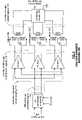
- FIG. 3is a schematic block diagram of an embodiment of a linear high powered integrated circuit transmitter 100 that may be used in the wireless communication device illustrated in FIG. 2 .
- the transmitter 100includes an up-conversion module 82 , a plurality of power amplifiers 84 - 1 through 84 - 3 , a plurality of baluns 102 - 106 and a combining module 120 .
- the transmitter 100may be implemented as an integrated circuit and may be fabricated in accordance with CMOS technology, or any other type of integrated circuit technology.
- the up-conversion module 82is operably coupled to mix a differential low IF signal 108 with a differential transmit local oscillation signal 83 .
- the output conversion module 82provides the differential up-converted signal 110 to the plurality of power amplifiers 84 - 1 through 84 - 3 via the balanced integrated circuit coupling 112 .
- the balanced integrated circuit coupling 112constitute metal traces formed on one or more layers of the integrated circuit and exhibit similar frequency response characteristics and impedances such that the coupling between each of the plurality of power amplifiers and the up-conversion module is substantially identical.
- Each of the power amplifiers 84 - 1 through 84 - 3may be of a similar construct, which includes a pair of input transistors to receive opposite phases of the differential up-converted signal 110 , loads coupled in series with each of the input transistors and a current source coupled to the sources of each transistor.
- the power amplifiersmay be constructed in a variety of ways to achieve the desired power amplification.
- Each of the power amplifiersamplifies the differential up-converted signal, or a signal, 110 to produce a plurality of differential amplified RF signals 114 .
- Each of the differential amplified RF signals 114is provided to a corresponding balun 102 - 106 .
- the baluns 102 - 106which may be transformer baluns or inductor/capacitor baluns, convert the differential amplified RF signals 114 into a plurality of single ended signals 116 .
- the combining module 120receives the plurality of single ended signals 116 and combines them to produce a single ended RF signal 118 .
- the combining module 120may be a power combiner, which is commercially available, or a combination of passive components such as inductors and/or capacitors.
- the combining module 120may be an on-chip device or an off-chip device.
- the coupling between the baluns and the combining module 120should be balanced.
- Such balanced IC couplingprovides similar impedances and frequency responses between the baluns and combining module. If the combining module 120 is off-chip, the balanced integrated circuit coupling is between the baluns 102 - 106 and the corresponding pins of the integrated circuit that includes transmitter 100 .
- the transmitter 100may further include the transmitter filtering module 85 as illustrated in FIG. 2 .
- a filtering module 85may be coupled to the output of the combining module 120 .
- the transmitter filtering module 85may include a plurality of differential filters coupled to the outputs of the power amplifiers.
- the transmitter filtering module 85may include a plurality of single-ended filters coupled to the outputs of the baluns 102 - 106 .
- FIG. 4is a schematic block diagram of another embodiment of a linear high powered integrated circuit transmitter 130 which may be used in the wireless communication device illustrated in FIG. 2 .
- the transmitter 130includes the up-conversion module 82 , the plurality of power amplifiers 84 - 1 through 84 - 3 , and a combining circuit 132 .
- the functionality, and construct, of the up-conversion module 82 , the balanced integrated circuit coupling 112 and the power amplifiers 84 - 1 through 84 - 3is as previously discussed with reference to FIG. 3 .
- the transmitter 130may be implemented as an integrated circuit and may be fabricated in accordance with CMOS technology, or any other type of integrated circuit technology.
- the combining circuit 132receives the plurality of differential amplified signals 114 from the power amplifiers 84 - 1 through 84 - 3 . Upon receiving these signals, the combining circuit 132 combines them to produce a single ended RF signal 118 . In one embodiment of the combining circuit 132 , it includes a plurality of baluns operably coupled to the plurality of power amplifiers and a combiner that combines the single ended signals produced by the baluns.
- the coupling between the power amplifiers and the combining circuit 132is balanced such that the impedances and frequency/gain responses of the coupling are balanced between each of the power amplifiers in the combining circuit 132 .
- the transmitter. 130may further include the transmit filter 85 as shown in FIG. 2 coupled after the combining circuit 132 .
- the transmit filtermay include a plurality of filters coupled to the outputs of the power amplifiers 84 - 1 through 84 - 3 .
- FIG. 5is a schematic block diagram of another embodiment of a linear high powered integrated transmitter 140 that may be used in the wireless communication device illustrated in FIG. 2 .
- the transmitter 140includes the up-conversion module 82 , the balanced integrated circuit coupling 112 , a plurality of current mode power amplifiers 84 -A through 84 -C, a current-to-voltage circuit 144 , an a balun 150 .
- the transmitter 140may be implemented as an integrated circuit and may be fabricated in accordance with CMOS technology, or any other type of integrated circuit technology.
- the up-conversion module 82produces the differential up-converted signal 110 by mixing the low IF signal 108 with the transmitter local oscillation 83 .
- the power amplifiers 84 -A through 84 -Camplify the differential up-converted signal 110 and produces amplified current signals, which are differential.
- the positive phases of each of the power amplifiers 84 -A through 84 -Care directly coupled together via direct coupling 142 to produce a positive combined current signal 146 .
- the negative phases of the power amplifier output 84 -A through 84 -Care directly combined via direct coupling 142 to produce a negative combined current signal 148 .
- the power amplifiers 84 -A through 84 -Care transconductance power amplifiers.
- the current-to-voltage circuit 144converts the positive and negative combined current signals 146 and 148 into a differential voltage signal.
- the current-to-voltage circuit 144may include resistors, inductors, capacitors and/or transistors to perform the current-to-voltage transformation.
- the balun 150which may be a transformer or inductor/capacitor circuit, receives the differential voltage and converts it into a single ended RF signal 118 .
- the transmit filter 85 as shown in FIG. 2may be included before or after the balun 150 .
Landscapes
- Engineering & Computer Science (AREA)
- Power Engineering (AREA)
- Computer Networks & Wireless Communication (AREA)
- Signal Processing (AREA)
- Amplifiers (AREA)
- Transmitters (AREA)
Abstract
Description
- 1. U.S. Utility application Ser. No. 10/200,959, entitled “LINEAR HIGH POWERED INTEGRATED CIRCUIT TRANSMITTER”, filed Jul. 23, 2002, now issued as U.S. Pat. No. 6,996,379, on Feb. 7, 2006.
Claims (14)
Priority Applications (2)
| Application Number | Priority Date | Filing Date | Title |
|---|---|---|---|
| US11/281,059US7551901B2 (en) | 2002-07-23 | 2005-11-16 | Linear high powered integrated circuit amplifier |
| US12/484,929US8000664B2 (en) | 2002-07-23 | 2009-06-15 | Linear high powered integrated circuit amplifier |
Applications Claiming Priority (2)
| Application Number | Priority Date | Filing Date | Title |
|---|---|---|---|
| US10/200,959US6996379B2 (en) | 2002-07-23 | 2002-07-23 | Linear high powered integrated circuit transmitter |
| US11/281,059US7551901B2 (en) | 2002-07-23 | 2005-11-16 | Linear high powered integrated circuit amplifier |
Related Parent Applications (1)
| Application Number | Title | Priority Date | Filing Date |
|---|---|---|---|
| US10/200,959ContinuationUS6996379B2 (en) | 2002-07-23 | 2002-07-23 | Linear high powered integrated circuit transmitter |
Related Child Applications (1)
| Application Number | Title | Priority Date | Filing Date |
|---|---|---|---|
| US12/484,929ContinuationUS8000664B2 (en) | 2002-07-23 | 2009-06-15 | Linear high powered integrated circuit amplifier |
Publications (2)
| Publication Number | Publication Date |
|---|---|
| US20060068723A1 US20060068723A1 (en) | 2006-03-30 |
| US7551901B2true US7551901B2 (en) | 2009-06-23 |
Family
ID=30769581
Family Applications (3)
| Application Number | Title | Priority Date | Filing Date |
|---|---|---|---|
| US10/200,959Expired - LifetimeUS6996379B2 (en) | 2002-07-23 | 2002-07-23 | Linear high powered integrated circuit transmitter |
| US11/281,059Expired - Fee RelatedUS7551901B2 (en) | 2002-07-23 | 2005-11-16 | Linear high powered integrated circuit amplifier |
| US12/484,929Expired - Fee RelatedUS8000664B2 (en) | 2002-07-23 | 2009-06-15 | Linear high powered integrated circuit amplifier |
Family Applications Before (1)
| Application Number | Title | Priority Date | Filing Date |
|---|---|---|---|
| US10/200,959Expired - LifetimeUS6996379B2 (en) | 2002-07-23 | 2002-07-23 | Linear high powered integrated circuit transmitter |
Family Applications After (1)
| Application Number | Title | Priority Date | Filing Date |
|---|---|---|---|
| US12/484,929Expired - Fee RelatedUS8000664B2 (en) | 2002-07-23 | 2009-06-15 | Linear high powered integrated circuit amplifier |
Country Status (1)
| Country | Link |
|---|---|
| US (3) | US6996379B2 (en) |
Cited By (2)
| Publication number | Priority date | Publication date | Assignee | Title |
|---|---|---|---|---|
| US20090251222A1 (en)* | 2002-07-23 | 2009-10-08 | Broadcom Corporation | Linear High Powered Integrated Circuit Amplifier |
| US20090305747A1 (en)* | 2004-11-16 | 2009-12-10 | St Wireless Sa | Apparatus for filtering a reference voltage and mobile phones comprising such apparatus |
Families Citing this family (96)
| Publication number | Priority date | Publication date | Assignee | Title |
|---|---|---|---|---|
| US6982609B1 (en)* | 2002-05-15 | 2006-01-03 | Zeevo | System method and apparatus for a three-line balun with power amplifier bias |
| US7092681B2 (en)* | 2002-07-23 | 2006-08-15 | Broadcom Corporation | High output power radio frequency integrated circuit |
| KR100489046B1 (en)* | 2002-08-27 | 2005-05-11 | 엘지전자 주식회사 | LPA Shelf |
| US7882346B2 (en)* | 2002-10-15 | 2011-02-01 | Qualcomm Incorporated | Method and apparatus for providing authentication, authorization and accounting to roaming nodes |
| US7869803B2 (en)* | 2002-10-15 | 2011-01-11 | Qualcomm Incorporated | Profile modification for roaming in a communications environment |
| US7444124B1 (en) | 2003-05-14 | 2008-10-28 | Marvell International Ltd. | Adjustable segmented power amplifier |
| US7157965B1 (en)* | 2004-06-21 | 2007-01-02 | Qualcomm Incorporated | Summing power amplifier |
| US7349679B1 (en)* | 2004-06-30 | 2008-03-25 | Qualcomm Inc. | Integrated power amplifier |
| US7684499B2 (en)* | 2005-08-30 | 2010-03-23 | 2Wire, Inc. | Multi-band line interface circuit with line side cancellation |
| US9066344B2 (en) | 2005-09-19 | 2015-06-23 | Qualcomm Incorporated | State synchronization of access routers |
| US7764245B2 (en)* | 2006-06-16 | 2010-07-27 | Cingular Wireless Ii, Llc | Multi-band antenna |
| US7630696B2 (en)* | 2006-06-16 | 2009-12-08 | At&T Mobility Ii Llc | Multi-band RF combiner |
| WO2008024551A2 (en)* | 2006-06-16 | 2008-02-28 | Cingular Wireless Ii Llc | Multi-resonant microstrip dipole antenna |
| US7277062B1 (en) | 2006-06-16 | 2007-10-02 | At&T Mobility Ii Llc | Multi-resonant microstrip dipole antenna |
| US7542735B2 (en)* | 2006-10-20 | 2009-06-02 | Northrop Grumman Corporation | Multi-octave differential upconverter |
| US7894780B2 (en)* | 2006-12-06 | 2011-02-22 | Broadcom Corporation | Method and system for a linearized transmitter including a power amplifier |
| US7756504B2 (en) | 2007-06-29 | 2010-07-13 | Silicon Laboratories Inc. | Rotating harmonic rejection mixer |
| US8260244B2 (en)* | 2007-06-29 | 2012-09-04 | Silicon Laboratories Inc. | Rotating harmonic rejection mixer |
| WO2009006189A2 (en)* | 2007-06-29 | 2009-01-08 | Silicon Laboratories Inc. | A rotating harmonic rejection mixer |
| US8538366B2 (en) | 2007-06-29 | 2013-09-17 | Silicon Laboratories Inc | Rotating harmonic rejection mixer |
| US7860480B2 (en) | 2007-06-29 | 2010-12-28 | Silicon Laboratories Inc. | Method and apparatus for controlling a harmonic rejection mixer |
| US8503962B2 (en)* | 2007-06-29 | 2013-08-06 | Silicon Laboratories Inc. | Implementing a rotating harmonic rejection mixer (RHRM) for a TV tuner in an integrated circuit |
| US8787850B2 (en)* | 2008-03-31 | 2014-07-22 | Avago Technologies General Ip (Singapore) Pte. Ltd. | Compensating for non-linear capacitance effects in a power amplifier |
| US8344808B2 (en) | 2008-03-31 | 2013-01-01 | Javelin Semiconductor, Inc. | Non-linear capacitance compensation |
| US7872528B2 (en)* | 2008-04-10 | 2011-01-18 | Javelin Semiconductor, Inc. | Providing pre-distortion to an input signal |
| US7728661B2 (en)* | 2008-05-05 | 2010-06-01 | Javelin Semiconductor, Inc. | Controlling power with an output network |
| US8160520B2 (en)* | 2008-05-09 | 2012-04-17 | Javelin Semiconductor, Inc. | Supply control for multiple power modes of a power amplifier |
| US7768350B2 (en)* | 2008-12-30 | 2010-08-03 | Javelin Semiconductor, Inc. | Output gain stage for a power amplifier |
| US8666340B2 (en)* | 2009-03-03 | 2014-03-04 | Broadcom Corporation | Method and system for on-chip impedance control to impedance match a configurable front end |
| US8068795B2 (en)* | 2009-03-24 | 2011-11-29 | Freescale Semiconductor, Inc. | RF multiband transmitter with balun |
| US8270499B2 (en)* | 2009-05-15 | 2012-09-18 | Qualcomm, Incorporated | Receiver with balanced I/Q transformer |
| US8536950B2 (en)* | 2009-08-03 | 2013-09-17 | Qualcomm Incorporated | Multi-stage impedance matching |
| US8102205B2 (en) | 2009-08-04 | 2012-01-24 | Qualcomm, Incorporated | Amplifier module with multiple operating modes |
| US9048802B2 (en) | 2009-08-17 | 2015-06-02 | Skyworks Solutions, Inc. | Radio frequency power amplifier with linearizing predistorter |
| US8116700B2 (en)* | 2009-11-16 | 2012-02-14 | Javelin Semiconductor, Inc. | Reducing common mode effects in an output stage |
| US8432218B1 (en)* | 2010-04-13 | 2013-04-30 | University Of Washington Through Its Center For Commercialization | Harmonic-rejection power amplifier |
| US9288089B2 (en) | 2010-04-30 | 2016-03-15 | Ecole Polytechnique Federale De Lausanne (Epfl) | Orthogonal differential vector signaling |
| US9985634B2 (en) | 2010-05-20 | 2018-05-29 | Kandou Labs, S.A. | Data-driven voltage regulator |
| US9124557B2 (en) | 2010-05-20 | 2015-09-01 | Kandou Labs, S.A. | Methods and systems for chip-to-chip communication with reduced simultaneous switching noise |
| US9077386B1 (en) | 2010-05-20 | 2015-07-07 | Kandou Labs, S.A. | Methods and systems for selection of unions of vector signaling codes for power and pin efficient chip-to-chip communication |
| US8593305B1 (en) | 2011-07-05 | 2013-11-26 | Kandou Labs, S.A. | Efficient processing and detection of balanced codes |
| US9251873B1 (en) | 2010-05-20 | 2016-02-02 | Kandou Labs, S.A. | Methods and systems for pin-efficient memory controller interface using vector signaling codes for chip-to-chip communications |
| US9288082B1 (en) | 2010-05-20 | 2016-03-15 | Kandou Labs, S.A. | Circuits for efficient detection of vector signaling codes for chip-to-chip communication using sums of differences |
| US9246713B2 (en) | 2010-05-20 | 2016-01-26 | Kandou Labs, S.A. | Vector signaling with reduced receiver complexity |
| WO2011151469A1 (en) | 2010-06-04 | 2011-12-08 | Ecole Polytechnique Federale De Lausanne | Error control coding for orthogonal differential vector signaling |
| US8786381B2 (en) | 2010-06-28 | 2014-07-22 | Avago Technologies General Ip (Singapore) Pte. Ltd. | Transformer structures for a power amplifier (PA) |
| US8571512B2 (en) | 2012-01-05 | 2013-10-29 | Silicon Laboratories Inc. | Implementing a passive rotating harmonic rejection mixer (RHRM) for a TV tuner in an integrated circuit |
| US9065386B2 (en) | 2012-02-29 | 2015-06-23 | Avago Technologies General Ip (Singapore) Pte. Ltd. | Low voltage operation for a power amplifier |
| US8897726B2 (en) | 2012-06-19 | 2014-11-25 | Qualcomm Incorporated | Block sharing using three-way transformers in wireless circuits |
| US9813086B2 (en)* | 2012-12-21 | 2017-11-07 | Mediatek Singapore Pte. Ltd | RF transmitter, integrated circuit device, wireless communication unit and method therefor |
| WO2014124450A1 (en) | 2013-02-11 | 2014-08-14 | Kandou Labs, S.A. | Methods and systems for high bandwidth chip-to-chip communications interface |
| CN110166217B (en) | 2013-04-16 | 2022-05-17 | 康杜实验室公司 | High bandwidth communication interface method and system |
| GB2514784B (en)* | 2013-06-03 | 2015-10-28 | Broadcom Corp | Signal Processing |
| EP2997704B1 (en) | 2013-06-25 | 2020-12-16 | Kandou Labs S.A. | Vector signaling with reduced receiver complexity |
| US9806761B1 (en) | 2014-01-31 | 2017-10-31 | Kandou Labs, S.A. | Methods and systems for reduction of nearest-neighbor crosstalk |
| US9100232B1 (en) | 2014-02-02 | 2015-08-04 | Kandou Labs, S.A. | Method for code evaluation using ISI ratio |
| KR102240544B1 (en) | 2014-02-28 | 2021-04-19 | 칸도우 랩스 에스에이 | Clock-embedded vector signaling codes |
| US9509437B2 (en) | 2014-05-13 | 2016-11-29 | Kandou Labs, S.A. | Vector signaling code with improved noise margin |
| US9148087B1 (en) | 2014-05-16 | 2015-09-29 | Kandou Labs, S.A. | Symmetric is linear equalization circuit with increased gain |
| US9852806B2 (en) | 2014-06-20 | 2017-12-26 | Kandou Labs, S.A. | System for generating a test pattern to detect and isolate stuck faults for an interface using transition coding |
| US9112550B1 (en) | 2014-06-25 | 2015-08-18 | Kandou Labs, SA | Multilevel driver for high speed chip-to-chip communications |
| EP3138253A4 (en) | 2014-07-10 | 2018-01-10 | Kandou Labs S.A. | Vector signaling codes with increased signal to noise characteristics |
| US9432082B2 (en) | 2014-07-17 | 2016-08-30 | Kandou Labs, S.A. | Bus reversable orthogonal differential vector signaling codes |
| KR101943048B1 (en) | 2014-07-21 | 2019-01-28 | 칸도우 랩스 에스에이 | Multidrop data transfer |
| WO2016019384A1 (en) | 2014-08-01 | 2016-02-04 | Kandou Labs, S.A. | Orthogonal differential vector signaling codes with embedded clock |
| US9674014B2 (en) | 2014-10-22 | 2017-06-06 | Kandou Labs, S.A. | Method and apparatus for high speed chip-to-chip communications |
| KR101978470B1 (en) | 2015-06-26 | 2019-05-14 | 칸도우 랩스 에스에이 | High-speed communication system |
| US10055372B2 (en) | 2015-11-25 | 2018-08-21 | Kandou Labs, S.A. | Orthogonal differential vector signaling codes with embedded clock |
| US10003315B2 (en) | 2016-01-25 | 2018-06-19 | Kandou Labs S.A. | Voltage sampler driver with enhanced high-frequency gain |
| US10003454B2 (en) | 2016-04-22 | 2018-06-19 | Kandou Labs, S.A. | Sampler with low input kickback |
| EP3446403B1 (en) | 2016-04-22 | 2021-01-06 | Kandou Labs S.A. | High performance phase locked loop |
| US10242749B2 (en) | 2016-04-22 | 2019-03-26 | Kandou Labs, S.A. | Calibration apparatus and method for sampler with adjustable high frequency gain |
| US10056903B2 (en) | 2016-04-28 | 2018-08-21 | Kandou Labs, S.A. | Low power multilevel driver |
| EP3449379B1 (en) | 2016-04-28 | 2021-10-06 | Kandou Labs S.A. | Vector signaling codes for densely-routed wire groups |
| US10153591B2 (en) | 2016-04-28 | 2018-12-11 | Kandou Labs, S.A. | Skew-resistant multi-wire channel |
| US9906358B1 (en) | 2016-08-31 | 2018-02-27 | Kandou Labs, S.A. | Lock detector for phase lock loop |
| US10411922B2 (en) | 2016-09-16 | 2019-09-10 | Kandou Labs, S.A. | Data-driven phase detector element for phase locked loops |
| US10200188B2 (en) | 2016-10-21 | 2019-02-05 | Kandou Labs, S.A. | Quadrature and duty cycle error correction in matrix phase lock loop |
| US10200218B2 (en) | 2016-10-24 | 2019-02-05 | Kandou Labs, S.A. | Multi-stage sampler with increased gain |
| US10372665B2 (en) | 2016-10-24 | 2019-08-06 | Kandou Labs, S.A. | Multiphase data receiver with distributed DFE |
| US10116468B1 (en) | 2017-06-28 | 2018-10-30 | Kandou Labs, S.A. | Low power chip-to-chip bidirectional communications |
| US10686583B2 (en) | 2017-07-04 | 2020-06-16 | Kandou Labs, S.A. | Method for measuring and correcting multi-wire skew |
| US10203226B1 (en) | 2017-08-11 | 2019-02-12 | Kandou Labs, S.A. | Phase interpolation circuit |
| US10326623B1 (en) | 2017-12-08 | 2019-06-18 | Kandou Labs, S.A. | Methods and systems for providing multi-stage distributed decision feedback equalization |
| US10554380B2 (en) | 2018-01-26 | 2020-02-04 | Kandou Labs, S.A. | Dynamically weighted exclusive or gate having weighted output segments for phase detection and phase interpolation |
| KR102707165B1 (en) | 2018-06-12 | 2024-09-13 | 칸도우 랩스 에스에이 | Passive multi-input comparator for orthogonal codes on multi-wire buses |
| US10931249B2 (en) | 2018-06-12 | 2021-02-23 | Kandou Labs, S.A. | Amplifier with adjustable high-frequency gain using varactor diodes |
| US11183983B2 (en) | 2018-09-10 | 2021-11-23 | Kandou Labs, S.A. | Programmable continuous time linear equalizer having stabilized high-frequency peaking for controlling operating current of a slicer |
| US10680634B1 (en) | 2019-04-08 | 2020-06-09 | Kandou Labs, S.A. | Dynamic integration time adjustment of a clocked data sampler using a static analog calibration circuit |
| US10721106B1 (en) | 2019-04-08 | 2020-07-21 | Kandou Labs, S.A. | Adaptive continuous time linear equalization and channel bandwidth control |
| US10608849B1 (en) | 2019-04-08 | 2020-03-31 | Kandou Labs, S.A. | Variable gain amplifier and sampler offset calibration without clock recovery |
| US10574487B1 (en) | 2019-04-08 | 2020-02-25 | Kandou Labs, S.A. | Sampler offset calibration during operation |
| US11303484B1 (en) | 2021-04-02 | 2022-04-12 | Kandou Labs SA | Continuous time linear equalization and bandwidth adaptation using asynchronous sampling |
| US11374800B1 (en) | 2021-04-14 | 2022-06-28 | Kandou Labs SA | Continuous time linear equalization and bandwidth adaptation using peak detector |
| US11456708B1 (en) | 2021-04-30 | 2022-09-27 | Kandou Labs SA | Reference generation circuit for maintaining temperature-tracked linearity in amplifier with adjustable high-frequency gain |
| US12355409B2 (en) | 2022-03-24 | 2025-07-08 | Kandou Labs SA | Variable gain amplifier with cross-coupled common mode reduction |
Citations (1)
| Publication number | Priority date | Publication date | Assignee | Title |
|---|---|---|---|---|
| US6816012B2 (en) | 2000-10-10 | 2004-11-09 | California Institute Of Technology | Distributed circular geometry power amplifier architecture |
Family Cites Families (10)
| Publication number | Priority date | Publication date | Assignee | Title |
|---|---|---|---|---|
| US4978959A (en)* | 1987-10-08 | 1990-12-18 | University Of Toronto Innovations Foundation | Analog to digital converter, a digital to analog converter and an operational amplifier therefor |
| US5126704A (en)* | 1991-04-11 | 1992-06-30 | Harris Corporation | Polyphase divider/combiner |
| US5574967A (en)* | 1994-01-11 | 1996-11-12 | Ericsson Ge Mobile Communications, Inc. | Waste energy control and management in power amplifiers |
| US6108529A (en)* | 1998-02-01 | 2000-08-22 | Bae Systems Aerospace Electronics Inc. | Radio system including FET mixer device and square-wave drive switching circuit and method therefor |
| US6889034B1 (en)* | 1998-04-02 | 2005-05-03 | Ericsson Inc. | Antenna coupling systems and methods for transmitters |
| US6115584A (en)* | 1999-04-02 | 2000-09-05 | Trw Inc. | Transmitter-receiver for use in broadband wireless access communications systems |
| US6285720B1 (en)* | 1999-05-28 | 2001-09-04 | W J Communications, Inc. | Method and apparatus for high data rate wireless communications over wavefield spaces |
| US6606483B1 (en)* | 2000-10-10 | 2003-08-12 | Motorola, Inc. | Dual open and closed loop linear transmitter |
| US6996379B2 (en)* | 2002-07-23 | 2006-02-07 | Broadcom Corp. | Linear high powered integrated circuit transmitter |
| US7092681B2 (en)* | 2002-07-23 | 2006-08-15 | Broadcom Corporation | High output power radio frequency integrated circuit |
- 2002
- 2002-07-23USUS10/200,959patent/US6996379B2/ennot_activeExpired - Lifetime
- 2005
- 2005-11-16USUS11/281,059patent/US7551901B2/ennot_activeExpired - Fee Related
- 2009
- 2009-06-15USUS12/484,929patent/US8000664B2/ennot_activeExpired - Fee Related
Patent Citations (1)
| Publication number | Priority date | Publication date | Assignee | Title |
|---|---|---|---|---|
| US6816012B2 (en) | 2000-10-10 | 2004-11-09 | California Institute Of Technology | Distributed circular geometry power amplifier architecture |
Cited By (4)
| Publication number | Priority date | Publication date | Assignee | Title |
|---|---|---|---|---|
| US20090251222A1 (en)* | 2002-07-23 | 2009-10-08 | Broadcom Corporation | Linear High Powered Integrated Circuit Amplifier |
| US8000664B2 (en)* | 2002-07-23 | 2011-08-16 | Broadcom Corporation | Linear high powered integrated circuit amplifier |
| US20090305747A1 (en)* | 2004-11-16 | 2009-12-10 | St Wireless Sa | Apparatus for filtering a reference voltage and mobile phones comprising such apparatus |
| US7912440B2 (en)* | 2004-11-16 | 2011-03-22 | St-Ericsson Sa | Apparatus for filtering a reference voltage and mobile phones comprising such apparatus |
Also Published As
| Publication number | Publication date |
|---|---|
| US20060068723A1 (en) | 2006-03-30 |
| US8000664B2 (en) | 2011-08-16 |
| US6996379B2 (en) | 2006-02-07 |
| US20090251222A1 (en) | 2009-10-08 |
| US20040198250A1 (en) | 2004-10-07 |
Similar Documents
| Publication | Publication Date | Title |
|---|---|---|
| US7551901B2 (en) | Linear high powered integrated circuit amplifier | |
| US7170465B2 (en) | RF diversity antenna coupling structure | |
| US7373116B2 (en) | High output power radio frequency integrated circuit | |
| US7697915B2 (en) | Gain boosting RF gain stage with cross-coupled capacitors | |
| US6882228B2 (en) | Radio frequency integrated circuit having an antenna diversity structure | |
| US7538741B2 (en) | Impedance matched passive radio frequency transmit/receive switch | |
| US7218909B2 (en) | Integrated low noise amplifier | |
| US7974599B2 (en) | Low noise amplifier with constant input impedance | |
| US7269391B2 (en) | Tunable transceiver front end | |
| US7129803B2 (en) | Tuned transformer balun circuit and applications thereof | |
| US7079816B2 (en) | On chip diversity antenna switch | |
| US6907231B2 (en) | On-chip impedance matching power amplifier and radio applications thereof | |
| US7391596B2 (en) | High frequency integrated circuit pad configuration including ESD protection circuitry | |
| US7184735B2 (en) | Radio frequency integrated circuit having symmetrical differential layout | |
| US7522394B2 (en) | Radio frequency integrated circuit having sectional ESD protection | |
| US20060066431A1 (en) | Adjustable differential inductor | |
| US7200370B2 (en) | Power amplifier having enhanced swing cascode architecture |
Legal Events
| Date | Code | Title | Description |
|---|---|---|---|
| FEPP | Fee payment procedure | Free format text:PAYOR NUMBER ASSIGNED (ORIGINAL EVENT CODE: ASPN); ENTITY STATUS OF PATENT OWNER: LARGE ENTITY | |
| STCF | Information on status: patent grant | Free format text:PATENTED CASE | |
| FPAY | Fee payment | Year of fee payment:4 | |
| AS | Assignment | Owner name:BANK OF AMERICA, N.A., AS COLLATERAL AGENT, NORTH CAROLINA Free format text:PATENT SECURITY AGREEMENT;ASSIGNOR:BROADCOM CORPORATION;REEL/FRAME:037806/0001 Effective date:20160201 Owner name:BANK OF AMERICA, N.A., AS COLLATERAL AGENT, NORTH Free format text:PATENT SECURITY AGREEMENT;ASSIGNOR:BROADCOM CORPORATION;REEL/FRAME:037806/0001 Effective date:20160201 | |
| FPAY | Fee payment | Year of fee payment:8 | |
| AS | Assignment | Owner name:AVAGO TECHNOLOGIES GENERAL IP (SINGAPORE) PTE. LTD., SINGAPORE Free format text:ASSIGNMENT OF ASSIGNORS INTEREST;ASSIGNOR:BROADCOM CORPORATION;REEL/FRAME:041706/0001 Effective date:20170120 Owner name:AVAGO TECHNOLOGIES GENERAL IP (SINGAPORE) PTE. LTD Free format text:ASSIGNMENT OF ASSIGNORS INTEREST;ASSIGNOR:BROADCOM CORPORATION;REEL/FRAME:041706/0001 Effective date:20170120 | |
| AS | Assignment | Owner name:BROADCOM CORPORATION, CALIFORNIA Free format text:TERMINATION AND RELEASE OF SECURITY INTEREST IN PATENTS;ASSIGNOR:BANK OF AMERICA, N.A., AS COLLATERAL AGENT;REEL/FRAME:041712/0001 Effective date:20170119 | |
| AS | Assignment | Owner name:AVAGO TECHNOLOGIES INTERNATIONAL SALES PTE. LIMITE Free format text:MERGER;ASSIGNOR:AVAGO TECHNOLOGIES GENERAL IP (SINGAPORE) PTE. LTD.;REEL/FRAME:047195/0827 Effective date:20180509 | |
| AS | Assignment | Owner name:AVAGO TECHNOLOGIES INTERNATIONAL SALES PTE. LIMITE Free format text:CORRECTIVE ASSIGNMENT TO CORRECT THE EFFECTIVE DATE OF MERGER PREVIOUSLY RECORDED AT REEL: 047195 FRAME: 0827. ASSIGNOR(S) HEREBY CONFIRMS THE MERGER;ASSIGNOR:AVAGO TECHNOLOGIES GENERAL IP (SINGAPORE) PTE. LTD.;REEL/FRAME:047924/0571 Effective date:20180905 | |
| FEPP | Fee payment procedure | Free format text:MAINTENANCE FEE REMINDER MAILED (ORIGINAL EVENT CODE: REM.); ENTITY STATUS OF PATENT OWNER: LARGE ENTITY | |
| LAPS | Lapse for failure to pay maintenance fees | Free format text:PATENT EXPIRED FOR FAILURE TO PAY MAINTENANCE FEES (ORIGINAL EVENT CODE: EXP.); ENTITY STATUS OF PATENT OWNER: LARGE ENTITY | |
| STCH | Information on status: patent discontinuation | Free format text:PATENT EXPIRED DUE TO NONPAYMENT OF MAINTENANCE FEES UNDER 37 CFR 1.362 | |
| FP | Lapsed due to failure to pay maintenance fee | Effective date:20210623 |