US7551492B2 - Non-volatile semiconductor memory with page erase - Google Patents
Non-volatile semiconductor memory with page eraseDownload PDFInfo
- Publication number
- US7551492B2 US7551492B2US11/715,838US71583807AUS7551492B2US 7551492 B2US7551492 B2US 7551492B2US 71583807 AUS71583807 AUS 71583807AUS 7551492 B2US7551492 B2US 7551492B2
- Authority
- US
- United States
- Prior art keywords
- voltage
- wordline
- wordlines
- erase
- substrate
- Prior art date
- Legal status (The legal status is an assumption and is not a legal conclusion. Google has not performed a legal analysis and makes no representation as to the accuracy of the status listed.)
- Active, expires
Links
Images


Classifications
- G—PHYSICS
- G11—INFORMATION STORAGE
- G11C—STATIC STORES
- G11C8/00—Arrangements for selecting an address in a digital store
- G11C8/08—Word line control circuits, e.g. drivers, boosters, pull-up circuits, pull-down circuits, precharging circuits, for word lines
- G—PHYSICS
- G11—INFORMATION STORAGE
- G11C—STATIC STORES
- G11C16/00—Erasable programmable read-only memories
- G11C16/02—Erasable programmable read-only memories electrically programmable
- G11C16/06—Auxiliary circuits, e.g. for writing into memory
- G11C16/10—Programming or data input circuits
- G11C16/14—Circuits for erasing electrically, e.g. erase voltage switching circuits
- G11C16/16—Circuits for erasing electrically, e.g. erase voltage switching circuits for erasing blocks, e.g. arrays, words, groups
- G—PHYSICS
- G11—INFORMATION STORAGE
- G11C—STATIC STORES
- G11C16/00—Erasable programmable read-only memories
- G11C16/02—Erasable programmable read-only memories electrically programmable
- G11C16/04—Erasable programmable read-only memories electrically programmable using variable threshold transistors, e.g. FAMOS
- G11C16/0483—Erasable programmable read-only memories electrically programmable using variable threshold transistors, e.g. FAMOS comprising cells having several storage transistors connected in series
- G—PHYSICS
- G11—INFORMATION STORAGE
- G11C—STATIC STORES
- G11C16/00—Erasable programmable read-only memories
- G11C16/02—Erasable programmable read-only memories electrically programmable
- G11C16/06—Auxiliary circuits, e.g. for writing into memory
- G11C16/10—Programming or data input circuits
- G11C16/14—Circuits for erasing electrically, e.g. erase voltage switching circuits
- G—PHYSICS
- G11—INFORMATION STORAGE
- G11C—STATIC STORES
- G11C16/00—Erasable programmable read-only memories
- G11C16/02—Erasable programmable read-only memories electrically programmable
- G11C16/06—Auxiliary circuits, e.g. for writing into memory
- G11C16/34—Determination of programming status, e.g. threshold voltage, overprogramming or underprogramming, retention
- G11C16/3436—Arrangements for verifying correct programming or erasure
- G11C16/344—Arrangements for verifying correct erasure or for detecting overerased cells
- G11C16/3445—Circuits or methods to verify correct erasure of nonvolatile memory cells
- G—PHYSICS
- G11—INFORMATION STORAGE
- G11C—STATIC STORES
- G11C7/00—Arrangements for writing information into, or reading information out from, a digital store
- G11C7/20—Memory cell initialisation circuits, e.g. when powering up or down, memory clear, latent image memory
Definitions
- Mobile electronic devicessuch as digital cameras, portable digital assistants, portable audio/video players and mobile terminals continue to require mass storage memory, preferably non-volatile memory with ever increasing capacities and speed capabilities.
- mass storage memorypreferably non-volatile memory with ever increasing capacities and speed capabilities.
- audio playerscan have between 256 Mbytes to 40 Gigabytes of memory for storing audio/video data.
- Non-volatile memorysuch as Flash memory and hard-disk drives are preferred since data is retained in the absence of power.
- Flash memoryalso known as solid-state drive, is popular because of their high density, non-volatility, and small size relative to hard disk drives. Flash memory technology is based on EPROM and EEPROM technologies. The term “flash” was chosen because a large number of memory cells could be erased at one time as distinguished from EEPROMs, where each byte was erased individually. Those of skill in the art will understand that Flash memory can be configured as NOR, NAND or other Flash, with NAND Flash having higher density per given area due to its more compact memory array structure. For the purpose of further discussion, references to Flash memory should be understood as being any type Flash memory.
- Each pageconsists of (j+k) bytes (x8b) as shown in FIG. 3 .
- the pagesare further divided into a j-byte data storage region (data field) with a separate k-byte area (spare field).
- the k-byte areais typically used for error management functions.
- the internal memory arrayis accessed on a page basis.
- the read operationstarts after writing READ command followed by addresses via common I/O pins (I/O 0 to I/O 7 ) to the device.
- the 2,112 bytes of data within the selected pageare sensed and transferred to the page register in less than tR (data transfer time from flash array to page register) shown in FIG. 4 .
- tRdata transfer time from flash array to page register
- the data in the data registercan be sequentially read from the device at, for example, 8 bits or 16 bits per cycle.
- the conventional memory arrayis programmed on a page basis.
- PROGRAM command followed by addresses and input data of 2,112 bytesis issued to the device through common I/O pins (I/O 0 to I/O 7 ).
- the 2,112 bytes of dataare transferred to the data register during input data loading cycles and finally programmed to the selected page of the cell array less than tPROG (page program time) as shown in FIG. 5 .
- the memory arrayis erased on a block basis.
- BLOCK ERASE command followed by block addressesis issued to the device through common I/O pins (I/O 0 to I/O 7 ).
- the 128K bytes of dataare erased less than tBERS (block erase time) as shown in FIG. 6 .
- tBERSblock erase time
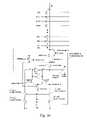
- a NAND cell stringtypically consists of one string selector transistor 71 , i memory cells 72 and one ground select transistor 73 which are serially connected as shown.
- FIG. 7The number (i) of cells per string can be varied by process technology, for example 8 cells per string or 16 cells per string or 32 cells per string. 32 memory cells per string are common in present 90 nm and 70 nm technologies. Hereinafter, ‘32’ is used for i as shown in FIG. 7 .
- Memory cell gatescorrespond to wordline 0 to 31 (W/L 0 to W/L 31 ).
- the gate of string select transistoris connected to a string select line (SSL) while the drain of string select transistor is connected to bitline (B/L).
- the gate of ground select transistoris connected to a ground select line (GSL) while the source of ground select transistor is connected to common source line (CSL).
- Each wordlinecorresponds to a page and each string corresponds to a block.
- FIGS. 8 and 9depict physical structure of a block with 32 cells per NAND cell string. As shown in FIG. 8 , there are (j+k)*8 NAND strings in a block. Thus the unit block has total (j+k)*8*32 cells. Each wordline is defined as unit page.
- FIG. 9shows n blocks Typically, flash memory cells are programmed and erased by either Fowler-Nordheim (F-N) tunneling or hot electron injection. In NAND flash memory, both erase and program are governed by F-N tunneling. The following erase and program operations are based on NAND flash memory.
- F-NFowler-Nordheim
- the top poly (i.e. top gate) of the cellis biased to Vss (ground) while the substrate of the cell is biased to erase voltage Vers (e.g. approximately 20 v, source and drain are automatically biased to Vers due to junction-forward-bias from P-substrate to n+ source/drain).
- Vssground
- Verserase voltage
- trapped electrons (charge) in the floating poly (i.e. floating gate)are emitted to the substrate through the tunnel oxide as shown in FIG. 10A .
- the cell Vth of the erased cellis negative value as shown in FIG. 10B .
- the erased cellis on-transistor (normally turn-on with gate bias Vg of 0V).
- the top poly (i.e. top gate) of the cellis biased to program voltage Vpgm (e.g. approximately 18 v) while the substrate, source and drain of the cell are biased to Vss (ground).
- Vpgmprogram voltage
- Vssground
- the floating polyi.e. floating gate
- the cell Vth of the programmed cellis positive value as shown in FIG. 11B .
- the programmed cellis off-transistor (normally turn-off with gate bias Vg of 0V).
- NAND flashis erased and programmed by a bi-directional (i.e. symmetrical) F-N tunneling mechanism.
- FIG. 12shows bias condition during erase operations.
- the p-well substrateis biased to erase voltage Vers while bitlines and the common source line (CSL) in the selected block are clamped to Vers-0.6 v through the S/D diodes of the SSL and GSL transistors.
- all wordlines in the selected blockare biased to 0V while the string select line (SSL) and the ground select line (GSL) are biased to erase voltage Vers. Therefore entire cells in the selected block are erased by F-N tunneling as described above.
- FIG. 13shows an erase inhibit scheme to unselected blocks:
- Table 1shows bias conditions for the selected block and unselected blocks with the prior art 1 during erase operations.
- the erase bias conditionsare substantially the same as above except the SSL and GSL are floating instead of biased to Vers, as shown in FIG. 14 .
- Table 2shows bias conditions during erase with this approach. There is no need to apply erase voltage Vers to wordlines in unselected blocks, which reduces power consumption during erase and reduces the erase time, because entire wordlines in unselected blocks are not needed to be biased to Vers.
- the erase operationmust occur on a block basis.
- the minimum erasable array sizeis a block.
- Flash memoriessuffer from three limitations. First, bits can be programmed only after erasing a target memory array. Second, each cell can only sustain a limited number of erasures, after which it can no longer reliably store data. In other words, there is a limitation in the number of erase and program cycles to cells (i.e. Endurance, typically 10,000 ⁇ 100,000 cycles). Third, the minimum erasable array size is much bigger than the minimum programmable array size. Due to these limitations, sophisticated data structures and algorithms are required to effectively use flash memories. (See for example, U.S. Pat. Nos. 5,937,425, 6732,221 and 6,594,183.
- a nonvolatile memory arraysuch as a NAND Flash Memory, has plural strings of memory cells on a substrate, wordlines across the strings to pages of memory cells and a pass transistor applying a voltage to each wordline.
- each pass transistor of a selected blockis enabled, for example through a block decoder.
- a wordline decodermay cause a select voltage to be applied to the pass transistor at each of plural selected wordlines of the selected block and an unselect voltage to be applied to the pass transistor at each of plural unselected wordlines of the selected block.
- a substrate voltageis applied to the substrate of the selected block.
- the voltage difference between the substrate voltage and a resulting voltage of each selected wordlinecauses the page of memory cells of the selected wordline to erase, and the voltage difference between the substrate voltage and the resulting voltage of each unselected wordline is less than that which erases the page of memory cells of the unselected wordline.
- a common select voltageis applied at each selected wordline and a common unselect voltage is applied at each unselected wordline.
- Select voltages and unselect voltagesmay be applied to any of the wordlines of a selected block.
- selected wordlinesmay be separated by at least one unselected wordline and unselected wordlines may be separated by at least one selected wordline.
- selected lines adjacent to unselected lineswhere boosting of a wordline is relied upon, the capacitive coupling that results in that boosting can be reduced.
- a higher initial voltage applied from the unselect voltageis preferred.
- the unselect voltagebe closer to the applied substrate voltage than to the select voltage.
- the resulting voltage of each selected wordlineis substantially the same as the select voltage and the resulting voltage of each unselected wordline is a floating voltage pulled from the unselect voltage toward the substrate voltage.
- a common gate signal applied to each pass transistor of the selected blockhas a value V 2 , the unselect voltage is great than V 2 and the unselected wordline precharges to V 2 ⁇ Vtn.
- V 2is substantially less than the applied substrate voltage but is preferably at least 50% of the applied substrate voltage. As such, the unselect voltage in a selected block is greater than the voltage typically applied to the pass transistors in an unselected block.
- the resultant voltage of each selected wordlineis substantially the same as the select voltage and the resulting voltage of each unselected wordline is substantially the same as the unselect voltage.
- the select voltagemay be about 0V and the unselect voltage may be about equal to the applied substrate voltage.
- a select verify voltagemay be applied to each wordline of plural erased pages in the selected block and an unselect verify voltage may be applied to each wordline of plural nonerased pages in the selected block.
- the state of strings of the selected blockis then sensed.
- Each stringis connected to an end voltage, specifically a source voltage.
- the level of the end voltagemay be selected from one of plural voltage levels dependent on the number of selected wordlines.
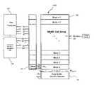
- FIG. 1NAND Flash Cell Array Structure.
- FIG. 2.NAND Flash Block Structure.
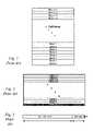
- FIG. 3.NAND Flash Page Structure.
- FIG. 4.Page Basis Read Operation in NAND Flash.
- FIG. 5.Page Basis Program Operation in NAND Flash.
- FIG. 6.Block Basis Erase Operation in NAND Flash.
- FIG. 7.NAND Cell String with 32 cells.
- FIG. 8.Block and Page Definition in NAND Flash.
- FIG. 9.Multiple Block in NAND Flash.
- FIG. 10AErase Operation by Fowler-Nordheim (F-N) Tunneling.
- FIG. 10BErase Operation by Fowler-Nordheim (F-N) Tunneling.
- FIG. 11AProgram Operation by Fowler-Nordheim (F-N) Tunneling.
- FIG. 12.Bias Conditions to Selected Block during Erase - Prior Art1.
- FIG. 13.Block Erase and Static Erase Inhibit Scheme - Prior Art 1.
- FIG. 14.Bias Conditions to Selected Block during Erase - Prior Art 2.
- FIG. 15.Block Erase and Self-boosting Erase Inhibit Scheme - Prior Art 2.
- FIG. 16.Block Copy Process to Modify a Page or a Portion of the Page.
- FIG. 17.Bias Conditions to Selected Block during Erase - Page Erase. Scheme 1
- FIG. 21Page Erase Bias Conditions - Page Erase Scheme 2B.
- FIG. 22Page Erase and Erase Inhibit - Page Erase Scheme 2B.
- FIG. 23Multiple Pages Erase - Page Erase Scheme 1.
- FIG. 24Multiple Pages Erase - Page Erase Scheme 2A.
- FIG. 25Multiple Pages Erase - Page Erase Scheme 2B.
- FIG. 26Block Erase - Page Erase Scheme 2A.
- FIG. 28Page Erase Verify without Source Bias.
- FIG. 29Page Erase Verify with Source Bias.
- FIG. 30Block Erase Verify.
- FIG. 31Page Erase Verify without Source Bias.
- FIG. 34Block Decoder Schematic for Page Erase Scheme 1.
- FIG. 35Block Decoder Schematic for Page Erase Scheme 2A and 2B.
- FIG. 36Page Buffer and Column Selector - Example.
- FIG. 37Page Erase/Multiple Page Erase Timing - Page Erase Scheme 1.
- FIG. 38Page Erase/Multiple Page Erase Timing - Page Erase Scheme 2A.
- FIG. 39Page Erase/Multiple Page Erase Timing - Page Erase Scheme 2B.
- FIG. 40
- FIG. 41Block Erase Timing - Page Erase Scheme 2A.
- FIG. 41Block Erase Timing - Page Erase Scheme 2B.
- FIG. 42Page Erase Verify Timing for Page Erase Scheme 1 with Source Bias.
- FIG. 43Block Erase Verify Timing for Page Erase Scheme 1.
- FIG. 44Page Erase Verify Timing for Page Erase Scheme 2A and 2B.
- FIG. 45Block Erase Verify Timing for Page Erase Scheme 2A and 2B.
- FIG. 46Bias Conditions to Selected Block during Erase - Page Erase Scheme 3.
- FIG. 47Bias Conditions to Selected Block during Erase - Page Erase Scheme 3.
- FIG. 48Page Erase and Erase Inhibit - Page Erase Scheme 3.
- FIG. 49Multiple Page Erase and Erase Inhibit - Page Erase Scheme 3.
- FIG. 50Parasitic capacitance during Page Erase Scheme 3.
- FIG. 51Page Erase/Multiple Page Erase Timing - Page Erase Scheme 3.
- the page sizeis 512 bytes, 2048 bytes, or 4096 byte while the block size is 16 pages, 32 pages, or 64 pages. Therefore the minimum erasable block size is at least 16 times larger than the page size. Moreover, this minimum size of erasable block (i.e. unit erase block) is getting bigger as the chip size increases.
- the array size mismatch between program/read and eraseintroduces two critical problems in device reliability (i.e. device lifetime) and system performance degradation in flash file system.
- flash memory cells in flash memory devicesmust be erased before being programmed by input data. Data write operations should be immediately executed once the CPU or flash controller in the system issues the program command. Thus the erase-before-program decreases overall system performance.
- the flash controllertypically prepares empty erased blocks in advance (i.e. Erase-unit Reclamation). This reclamation can take place either in the background (when the CPU is idle) or on-demand when the amount of free space drops below a predetermined threshold.
- the block containing a page to be modifiedwill be rewritten to one of free (empty) blocks declared by the erase-unit reclamation.
- valid pages containing original data in the original blockshould be copied to the selected free block as shown in FIG. 16 .
- the modified pageis read, modified and copied to the new block then, the new block having modified data in a page with original data in the rest of pages is remapped to the valid block address by a virtual mapping system in the flash controller.
- the virtual mapping systemis an address translation system between logical addresses accessed by the flash controller and physical addresses in the flash memory.
- NAND flash devicessupport a page copy function without external transaction between flash devices and the flash controller. Nevertheless, the array size mismatch between program/read and erase operations introduces a huge system overhead and complexity.
- the flash memory cellis programmed and erased by either Fowler-Nordheim tunneling or hot electron injection.
- chargeis transferred to or from a floating gate through the dielectric surrounding the floating gate. This frequent charge transfer causes electrons to be trapped in the floating gate and the dielectric, which degrades program and erase characteristics of cells.
- Consequent cellsrequire gradually higher program voltage and erase voltage due to this electron trapping with an increasing number of erase-program cycles; as a result, the number of erase-program cycles on a cell is limited.
- the maximum number of erase-program cyclei.e. cell endurance characteristic
- the limited number of erase-program cycleslimits the lifetime of a flash device. It would be advantageous to have a lifetime that is as long as possible, and this depends on the pattern of access to the flash device. Repeated and frequent rewrites to a single cell or small number of cells will bring the onset of failures soon and end the useful lifetime of the device quickly
- the flash memory systemhaving multiple flash devices, if there is significantly uneven use among devices in the flash memory system, one device reaches an end of lifetime while other devices have significant life left in them. When the one device reaches an end of lifetime, the entire memory system may have to be replaced, and this greatly reduces the life time of the flash memory system.
- Each NAND cell string in the NAND flash memorycan be controlled independently although the cell substrate is common across NAND cell strings of the device. All wordlines in a block during erase operations are biased to the same voltage condition in typical NAND flash devices. This is why the minimum erasable array size is a block in the NAND flash memory.
- each wordline corresponding to a page of the NAND cell stringmust be controlled separately and independently.
- Table 3 and FIG. 17show bias conditions during page erase according to a page erase scheme 1 (for example, erase of wordline 27 ).
- a page erase scheme 1for example, erase of wordline 27 .
- unselected wordlinesare biased to a voltage for preventing the unselected page(s) from being erased, for example, Vers while the selected wordline(s) is(are) biased to another voltage for erasing the selected page(s), for example, 0V.
- all wordlines in unselected blocksare floated during erase operations, which is the same as the prior art 2, while bias conditions shown in Table 3 are applied to the selected block as shown in FIG. 18 . Therefore floated wordlines in unselected blocks are boosted to nearly erase voltage Vers by capacitive coupling between the substrate and wordlines in unselected blocks as applying erase voltage Vers to the substrate. (The wordlines are boosted to about 90% of Vers when the substrate of the cell array goes to Vers; however, boosted voltage level on floated wordlines is determined by coupling ratio between the substrate and wordlines.) The boosted voltage on wordlines in unselected blocks reduces electric field between the substrate and wordlines; as a result, erasure of memory cells in unselected blocks is prevented.
- the bias condition for the page erase schemes 2A and 2Bis as follows:
- FIG. 19shows voltage bias condition with the page erase scheme 2A to selected page (wordline 27 in this example) in the selected block during erase operation.
- the selected wordline 27 (page)is biased to negative voltage ⁇ 18V ( ⁇ V 1 ) while unselected wordlines are biased to 0V.
- V 20V
- Table 4 and FIG. 20show bias conditions for the selected block and unselected blocks. All wordlines of unselected blocks are floating during erase; hence the potential of all wordlines remain at 0V because the substrate is biased to 0V and all wordlines of unselected blocks are discharged to 0V before being floated for the erase.
- FIG. 21shows voltage bias condition with the page erase scheme 2B to a selected page (wordline 27 in this example) in the selected block during erase operation.
- the selected wordline 27 (page)is biased to negative voltage ⁇ 13V ( ⁇ V 1 ) while unselected wordlines are biased to 0V.
- the substrate of the cell arrayis biased to 5V. Total electric field between the gate and the substrate of cells is the same as that of the first example. Voltage to the substrate should be determined not to introduce erase disturbance (i.e. soft-erase) to cells on the unselected wordlines (pages) in the same NAND cell string.
- Table 5 and FIG. 22show bias conditions for the selected block and unselected blocks. All wordlines of unselected blocks are floating during erase operations, all wordlines of unselected blocks are boosted to nearly the substrate voltage by capacitive coupling between the substrate and wordlines in unselected blocks as applying voltage to the substrate. (The boosted voltage is about 90% of substrate voltage; however boosted voltage level on floated wordlines is determined by coupling ratio between the substrate and wordlines) The boosted voltage on wordlines in unselected blocks reduces electric field between the substrate and wordlines; as a result, erasure of memory cells in unselected blocks is prevented.
- multiple pages (wordlines) in the selected blockcan be erased.
- any one or more pages of a selected blockmay be erased.
- entire pages of the selected blockcan be also erased, which is basically block erase.
- FIG. 23shows three pages (wordline 1 , 27 , 29 ) in the selected block are erased at the same time using bias conditions of the page erase scheme 1.
- FIG. 24shows three pages (wordline 1 , 27 , 29 ) in the selected block are erased at the same time using bias condition of the page erase scheme 2A.
- FIG. 25shows three pages (wordline 1 , 27 , 29 ) in the selected block are erased at the same time using bias condition of the page erase scheme 2B.
- FIG. 26shows all pages in the selected block are erased at the same time using bias condition of the page erase scheme 2A, which is the block erase.
- FIG. 27shows all pages in the selected block are erased at the same time using bias condition of the page erase scheme 2B, which is the block erase.
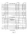
- FIG. 28 , FIG. 29 , FIG. 30 , and Table 6show voltage bias conditions during page erase verify and block erase verify. For multiple page verify, each selected page maybe verified consecutively (sequentially) after erase, but in a preferred approach, all are verified at once. Voltage numbers (i.e. Vread, Versvf, Vcslevf and Vbersvf) in Table 6 can be varied in accordance with process technology and cell characteristic.
- FIG. 28shows single page erase verify without source bias
- FIG. 29shows single page erase verify with source bias from CSL
- FIG. 30shows block erase verify.
- the final column of Table 6shows the block erase verify where all wordlines are selected. Those conditions can be compared to a conventional block erase verify. 0 volts, or for a less tolerant verification, a minus voltage such as ⁇ 1.5V, is applied to each wordline. As can be seen by reference to FIG. 10B , a properly erased memory cell will conduct with 0 volts applied to the wordline. If, however, the memory cell has not been fully erased, the memory cell will conduct less or not at all. In the block erase verify, any one of the memory cells failing to fully conduct will result in a higher voltage on the bitline that can be sensed as a failure to fully erase.
- each of the other memory cells of the stringmay be in either on state or off state.
- a high voltage of, for example, 4-5Vis applied to the wordline of each unselected cell. That voltage is higher than the threshold voltage even when the cell has been programmed to the off state as seen in FIG. 11B .
- the cellwill conduct even where it is been programmed to the off state, and all unselected memory cells will conduct. Setting the selected wordline to zero volts enables verification of just that selected wordline.
- a lower voltage on the bit line than is typical during a verify operationwould be expected.
- a negative voltagesuch as ⁇ 1.5 volts in the second column of Table 6
- a voltage higher than zero voltssuch as 0.4V shown in column one of Table 6
- the selected memory cellmust be more conductive for verification to offset the higher conductance of the unselected cells.
- the page erase verify with positive common source biasis generally preferred.
- Appropriate voltages of the common source linemight, for example, fall in the range of 0.3V-0.5V for a single page. For multiple page erase verify of less than a full block, lesser voltages are appropriate. For example, with a 0V common source voltage for a full block erase verify and 0.5V for a 1 page verify, it might be appropriate to decrease the source voltage from 0.5V by increments of 0.5/32 for each additional page being verified at once with the first page. Such fine control of the source voltage should not be required. However, the source voltage of 0.5V might, for example be used for verification of 0 through 8 selected wordlines at once, 0.4V might be used for verification of 9 through 16 select wordlines, 0.3V for 17-24 wordlines and 0V for 25-32 wordlines.
- erase operationsdo not require multiple erase and erase verify cycles since the threshold voltage of cells after a single erase and erase verify cycle is tightly distributed to the target value.
- multiple erase and erase verify cyclesalso can be applied to ensure target threshold voltage of erased cells
- FIG. 31shows a page erase flow using a single erase and erase verify cycle while FIG. 32 shows a page erase flow using multiple erase and erase verify cycles.
- the maximum number of erase and erase verify cycles for the multiple erase and erase verify cycles methodis predetermined and will be varied in accordance with process technology and cell characteristic. This page erase algorithm (flow) is automatically performed after issuing a page erase command in flash memory devices
- one or more selected pagesare erased.
- that one or more pagesare verified to have been erased.
- the status registeris updated to pass at 314 , and if not, it is updated to fail at 315 .
- a value ERS_loopis set to one at 320 .
- the ERS_loop valueis compared to a maximum at 321 . If the maximum has not been reached, the value is incremented at 322 and the erase and verify procedures are repeated. Once the maximum number of loops has been reached, the failure is indicated in the register at 315 .
- each selected pagemay be verified individually.
- the multiple page erasemay be repeated after the failure of any one page, or only failed pages may be again erased.
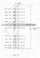
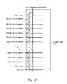
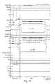
- FIG. 33depicts a simplified block diagram of NAND flash core.
- the NAND cell array 331comprises n blocks 332 like conventional NAND flash.
- the page buffer circuit 333senses and latches cell data during read, program verify and erase verify. Also the page buffer circuit temporarily holds input data and determines the voltage of bitlines in accordance with input data during program operations. All (j+k)*8 bitlines from the NAND cell array are connected to the page buffer circuit.
- the block decoder 334 corresponding to each NAND cell blockprovides signals as SSL (String Select Line), wordline 0 (WL 0 ) to 31 (WL 31 ) and GSL (ground select line).
- Block decodersare driven by row predecoded address signals Xp/Xq/Xr/Xt, from row predecoder 335 , and string select signal SS, ground select signal GS and common string decode signals S 0 to S 31 from common wordline decoder 336 .
- a substrate voltageis applied to the PP-well from a charge pump 337 .
- the NAND cell arrayconsists of n blocks and each block is subdivided into 32 (m) erasable and programmable pages (i.e. wordlines). There are (j+k)*8 bitline in the NAND cell array. Note that the number of block n, the number of page m and the number of (j+k)*8 can be varied.
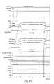
- FIG. 34illustrates a circuit schematic of block decoder which is one of possible examples for this invention, especially for the page erase scheme 1. Note that there are many variations on circuit implementation for the block decoder.
- the total number of the block decoderis n.
- the string select line SSL, wordlines WL 0 to WL 31 and the ground select line GSLare driven by common signals of SS, S 0 to S 31 and GS through pass transistors TSS, TS 0 to TS 31 and TGS which are commonly controlled by the output signal BD_out of the block decoder.
- the local charge pump 341is a high voltage switching circuit to provide program voltage Vpgm, pass voltage Vpass, read voltage Vread 7 , and erase voltage Vers. It consists of enhancement NMOS transistor (ENH), depletion NMOS transistor (DEP), native NMOS transistor (NAT) and a 2-input NAND gate G 1 .
- ENHenhancement NMOS transistor
- DEPdepletion NMOS transistor
- NATnative NMOS transistor
- the output signal BD_out of the block decoderis raised to Vhv when the block decoder latch output BDLCH_out is Vdd, HVenb is 0V and the OSC is oscillated (note: the local charge pump is a well known circuit technique).
- the BDLCH_outis reset to 0V when the RST_BD to the block decode reset transistor is high (actually short pulse) and latched when the LCHBD input to the block decode enable transistor is high (actually short pulse) with valid row predecoded address signals of Xp, Xq, Xr and Xt to NAND gate G 2 .
- BDLCH_outis latched by inverters I 1 and I 2 .
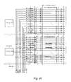
- FIG. 35illustrates a circuit schematic of block decoder for the page erase schemes 2A and 2B. Note that there are many variations on circuit implementation for the block decoder.
- the total number of the block decodersis n.
- the string select line SSL, wordlines WL 0 to WL 31 and the ground select line GSLare driven by common signals of SS, S 0 to S 31 and GS through pass transistors TSS, TS 0 to TS 31 and TGS which are commonly controlled by the output signal BD_out of the block decoder.
- the substrate of pass transistors TSS, TS 0 to TS 31 and TGSare controlled by the negative high voltage Vnhv.
- the high voltage level shifter 351is a high voltage switching circuit to provide positive high voltage Vhv and negative high voltage Vnhv.
- the level shifter circuitincludes cross-coupled p-channel transistors Q 1 and Q 2 and n-channel pull down devices Q 3 and Q 4 .
- BD_outis pulled high as Vhv is applied through Q 1
- Bd_outis pulled low to Vnhv through Q 4 .
- the BD_outis reset to 0V when the RST_BD is high (actually short pulse) and latched by inverters I 1 and I 2 when the LCHBD is high (actually short pulse) with valid row predecoded address signals of Xp, Xq, Xr and Xt to gate G 2 .
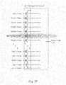
- Table 7shows an example of Vhv and Vnhv condition for various operating modes. All voltage numbers can be changed.
- Vread7V PROGRAM ⁇ 18 V 0 V PROGRAM ⁇ 7 V
- Vread70 V VERIFY ERASE VDD ⁇ 18 V OR ⁇ 13 V ERASE VERIFY ⁇ 7 V (Vread7) ⁇ 1.5 V OR 0 V
- the page buffer and column selector circuitis the same as that in conventional NAND flash as shown in FIG. 36 . Again the page buffer and column selector circuit shown in FIG. 36 is one of possible examples for this invention.
- One page buffercorresponds to one bitline.
- the page buffercan be shared by multiple bitlines as the array density increases (refer to reference June Lee et al., “A 90-nm CMOS 1.8-V 2-Gb NAND Flash Memory for Mass Storage Applications,” IEEE J Solid-State Circuits, vol. 38, no. 11, pp. 1934-1942, November 2003, incorporated by reference in its entirety.)
- the page buffer and column selector circuit of FIG. 36is used in read, program verify and erase verify operations.
- the erase verify operationthe latch is reset by LCHDA to latch node B high.
- the bitline BLis precharged to Vcc. If all selected memory cells are properly erased, the string of memory cells will conduct during the erase verify operation, thus pulling the bitline and node PBSO low.
- the bitline isolation transistorremains off. With PBSO less than about 0.5 v, the sense transistor below the latch will not turn on, so node B remains high. The high voltage on the B node keeps the pass/fail p-channel sense transistor off. As a result, that sense transistor will not charge the initially grounded line PASSb. If all strings are properly erased, the line PASSb remains low and a “pass” is sensed from that line.
- node PBSOIf, on the other hand, any string has not fully erased, the voltage on node PBSO will remain sufficiently high to turn on the sense transistors as LCHDB is asserted. As a result, node B is pulled low. With node B low on any of the page buffers in the selected block, a pass/fail sense transistor will turn on and raise PASSb to a high level. That high level is sensed to indicate a “fail”.
- FIG. 37shows the core timing of page erase or multiple page erase with the page erase scheme 1
- the erase operationconsists of three sub-periods as Erase Setup (from t 1 to t 2 ), Erase (t 2 to t 3 ) and Erase Recovery (from t 3 to t 4 ) shown in FIG. 37 .
- FIG. 38shows the core timing of page erase or multiple page erase with the page erase scheme 2A.
- FIG. 39shows the core timing of page erase or multiple page erase using the page erase scheme 2B with ⁇ V 1 of ⁇ 13V and V 2 of 5V.
- FIG. 40shows the core timing of block erase using the page erase scheme 2A with ⁇ V 1 of ⁇ 18V and V 2 of 0V.
- FIG. 41shows the core timing of block erase using the page erase scheme 2B with ⁇ V 1 of ⁇ 13V and V 2 of 5V.
- Erase verify operationconsists of five sub-periods as Erase Verify Setup (from t 1 to t 2 ), BL Precharge (t 2 to t 3 ), BL Sense (from t 3 to t 4 ), Data Latch (from t 4 to t 5 ) and Erase Verify Recovery (from t 5 to t 6 ) shown in FIG. 42 , FIG. 43 , FIG. 44 and FIG. 45 .
- FIG. 42shows the core timing of page erase verify for the page erase scheme 1.
- the voltage level of voltage sources described in hereis possible example and can be varied.
- selected pagesare verified sequentially (i.e. erase verify in a page basis).
- FIG. 43shows the core timing of block erase verify with the page erase scheme 1.
- the core signal timing the block erase verifyis basically the same as that of the page erase verify. However differences are:
- FIG. 44shows the core timing of page erase verify for the page erase scheme 2A and 2B.
- the voltage level of voltage sources described in hereis possible example and can be varied.
- selected pagesare verified sequentially (i.e. erase verify in a page basis).
- FIG. 45shows the core timing of block erase verify.
- the core signal timing the block erase verifyis basically the same as that of the page erase verify. However differences are:
- Table 8 and FIGS. 46 and 47show bias conditions during page erase according to a page erase scheme 3.
- FIGS. 48 and 49depict page erase conditions for unselected blocks, and selected page and unselected pages in the selected block.
- the capacitive coupling factor ⁇is dependent on individual wordline selection. Whereas, in an unselected block, ⁇ is approximately 90% at each wordline, ⁇ can be reduced adjacent to a selected wordline. The coupling is dependent on circuit characteristics but may reduce ⁇ to 50% as illustrated in FIG. 50 . Given the reduced coupling, the initial voltage of the wordline should be higher in order to assure that the wordline floats to a level that prevents erase.
- V 1 applied to the drain in the pass transistormust be greater than V 2 applied to the gate.
- wordline WL 28is boosted to close to Vers and will thus avoid accidental erasure.
- wordline WL 28is only raised to ⁇ 11 volts, resulting in >9 volts difference between the wordline and the substrate voltage Vers. As a result, unintended erasure of WL 28 is likely.
- the wordlineshould be at least about 70% Vers, or 14 volts in this example.
- the boosted voltage on the adjacent wordline WL 28is sufficiently high at 14.6 v.
- the reduced value of ⁇ and the acceptable voltage difference between the wordline and substratewill vary, thus varying the acceptable level of V 2 .
- V 2should be at least about 50% Vers. More generally, V 2 and thus V 1 should be closer to the substrate voltage than to the select voltage applied to pass transistors of selected wordlines.
- FIG. 49shows multiple pages (wordline 1 , 27 , 29 ) in the selected block are erased at the same time using bias conditions of the page erase scheme 3.
- FIG. 34illustrates a circuit schematic of block decoder which is one of possible examples for the page erase scheme 3 with V 1 >V 2 .
- the BDLCH_outis reset to 0V when the RST_BD is high (actually short pulse) and latched when the LCHBD is high (actually short pulse) with valid row predecoded address signals of Xp, Xq, Xr and Xt.
- the final output signal BD_out of the block pre-decoderis commonly connected to the gate of all pass transistors TSS, TS 0 to TS 31 and TGS.
- the string select line SSL, wordlines WL 0 to WL 31 and the ground select line GSLare driven by common signals of SS, S 0 to S 31 and GS through pass transistors which are commonly controlled by the output signal BD_out of the block pre-decoder.
- the local charge pumpis a high voltage switching mean to provide V 2 to the output signal BD_out of the block decoder. It consists of enhancement NMOS transistor, depletion NMOS transistor (DEP), native NMOS transistor (NAT) and a 2-input NAND gate.
- FIG. 51shows the core timing of page erase or multiple page erase with the page erase scheme 3.
- the erase operationconsists of three sub-periods as Erase Setup (from t 1 to t 2 ), Erase (t 2 to t 3 ) and Erase Recovery (from t 3 to t 4 ) shown in FIG. 51 .
Landscapes
- Engineering & Computer Science (AREA)
- Microelectronics & Electronic Packaging (AREA)
- Read Only Memory (AREA)
- Semiconductor Memories (AREA)
- Non-Volatile Memory (AREA)
Abstract
Description
- 1 page=(j+k) bytes.
- 1 block=m pages=(j+K) bytes*m.
- Total memory array size=n blocks=(j+K) bytes*m*n.
- All wordlines in the selected block are biased to 0V.
- All wordlines in unselected blocks are biased to Vers to compensate electrical field by Vers from the substrate.
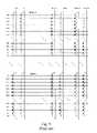
| TABLE 1 |
| Bias Conditions during Erase - |
| SELECTED | UNSELECTED | ||
| BLOCK | BLOCK | ||
| BITLINES (B/L) | CLAMPED | CLAMPED | ||
| TO Vers - 0.6 V | TO Vers - 0.6 V | |||
| STRING SELECT | Vers | Vers | ||
| LINE (SSL) | ||||
| 0 V | Vers | |||
| (W/L0~W/L31) | ||||
| GROUND SELECT | Vers | Vers | ||
| LINE (GSL) | ||||
| COMMON SOURCE | CLAMPED | CLAMPED | ||
| LINE (CSL) | TO Vers - 0.6 V | TO Vers - 0.6 V | ||
| SUBSTRATE | Vers | Vers | ||
| (POCKET P-WELL) | ||||
- All wordlines in the selected block are biased to 0V.
- All wordlines in unselected blocks are floating.
| TABLE 2 |
| Bias Conditions during Erase - |
| SELECTED BLOCK | UNSELECTED BLOCK | ||
| BITLINES (B/L) | CLAMPED TO Vers - | CLAMPED TO Vers - 0.6 V |
| 0.6 V | ||
| STRING SELECT | BOOSTED TO APPROX. | BOOSTED TO APPROX. |
| LINE (SSL) | 90% OF | 90% OF Vers |
| WORDLINES (W/L0~W/L31) | 0 V | BOOSTED TO APPROX. |
| 90% OF Vers | ||
| GROUND SELECT | BOOSTED TO APPROX. | BOOSTED TO APPROX. |
| LINE (GSL) | 90% OF | 90% OF Vers |
| COMMON SOURCE | CLAMPED TO Vers - | CLAMPED TO Vers - 0.6 V |
| LINE (CSL) | 0.6 V | |
| SUBSTRATE | Vers | Vers |
| (POCKET P-WELL) | ||
| FIG. 1. | NAND Flash Cell Array Structure. |
| FIG. 2. | NAND Flash Block Structure. |
| FIG. 3. | NAND Flash Page Structure. |
| FIG. 4. | Page Basis Read Operation in NAND Flash. |
| FIG. 5. | Page Basis Program Operation in NAND Flash. |
| FIG. 6. | Block Basis Erase Operation in NAND Flash. |
| FIG. 7. | NAND Cell String with 32 cells. |
| FIG. 8. | Block and Page Definition in NAND Flash. |
| FIG. 9. | Multiple Block in NAND Flash. |
| FIG. 10A. | Erase Operation by Fowler-Nordheim (F-N) Tunneling. |
| FIG. 10B. | Erase Operation by Fowler-Nordheim (F-N) Tunneling. |
| FIG. 11A. | Program Operation by Fowler-Nordheim (F-N) Tunneling. |
| FIG. 11B. | Program Operation by Fowler-Nordheim (F-N) Tunneling. |
| FIG. 12. | Bias Conditions to Selected Block during Erase - Prior Art1. |
| FIG. 13. | Block Erase and Static Erase Inhibit Scheme - |
| FIG. 14. | Bias Conditions to Selected Block during Erase - |
| FIG. 15. | Block Erase and Self-boosting Erase Inhibit Scheme - |
| Art | |
| 2. | |
| FIG. 16. | Block Copy Process to Modify a Page or a Portion of |
| the Page. | |
| FIG. 17. | Bias Conditions to Selected Block during Erase - Page Erase. |
| FIG. 18. | Page Erase and Erase Inhibit - Page Erase |
| FIG. 19. | Page Erase Bias Conditions - Page Erase Scheme 2A. |
| FIG. 20. | Page Erase and Erase Inhibit - Page Erase Scheme 2A. |
| FIG. 21. | Page Erase Bias Conditions - Page Erase Scheme 2B. |
| FIG. 22. | Page Erase and Erase Inhibit - Page Erase Scheme 2B. |
| FIG. 23. | Multiple Pages Erase - Page Erase |
| FIG. 24. | Multiple Pages Erase - Page Erase Scheme 2A. |
| FIG. 25. | Multiple Pages Erase - Page Erase Scheme 2B. |
| FIG. 26. | Block Erase - Page Erase Scheme 2A. |
| FIG. 27. | Block Erase - Page Erase Scheme 2B. |
| FIG. 28. | Page Erase Verify without Source Bias. |
| FIG. 29. | Page Erase Verify with Source Bias. |
| FIG. 30. | Block Erase Verify. |
| FIG. 31. | Page Erase Flow - Single Erase & Erase Verify Cycle. |
| FIG. 32. | Page Erase Flow - Multiple Erase & Erase Verify Cycle. |
| FIG. 33. | Simplified Block Diagram of NAND Flash Core. |
| FIG. 34. | Block Decoder Schematic for Page Erase |
| FIG. 35. | Block Decoder Schematic for Page Erase Scheme 2A and 2B. |
| FIG. 36. | Page Buffer and Column Selector - Example. |
| FIG. 37. | Page Erase/Multiple Page Erase Timing - Page Erase |
| FIG. 38. | Page Erase/Multiple Page Erase Timing - Page Erase |
| Scheme 2A. | |
| FIG. 39. | Page Erase/Multiple Page Erase Timing - Page Erase |
| Scheme 2B. | |
| FIG. 40. | Block Erase Timing - Page Erase Scheme 2A. |
| FIG. 41. | Block Erase Timing - Page Erase Scheme 2B. |
| FIG. 42. | Page Erase Verify Timing for Page Erase |
| Source Bias. | |
| FIG. 43. | Block Erase Verify Timing for Page Erase |
| FIG. 44. | Page Erase Verify Timing for Page Erase Scheme 2A and 2B. |
| FIG. 45. | Block Erase Verify Timing for Page Erase Scheme 2A |
| and 2B. | |
| FIG. 46. | Bias Conditions to Selected Block during Erase - Page Erase |
| FIG. 47. | Bias Conditions to Selected Block during Erase - Page Erase |
| FIG. 48. | Page Erase and Erase Inhibit - Page Erase |
| FIG. 49. | Multiple Page Erase and Erase Inhibit - Page Erase |
| FIG. 50. | Parasitic capacitance during Page Erase |
| FIG. 51. | Page Erase/Multiple Page Erase Timing - Page Erase |
- Selected wordline(s) in the selected block is(are) biased to 0V for erase, and
- Unselected wordline(s) in the selected block is(are) biased to Vers for erase inhibit.
- All wordlines in unselected blocks are floating.
| TABLE 3 |
| Bias Conditions during Page Erase - Page Erase |
| SELECTED BLOCK | UNSELECTED BLOCK | ||
| BITLINES (B/L) | CLAMPED TO Vers - | CLAMPED TO |
| 0.6 V | Vers - 0.6 V | |
| STRING | BOOSTED TO | BOOSTED TO APPROX. |
| SELECT | APPROX. 90% OF | 90% OF Vers |
| LINE (SSL) | ||
| SELECTED | 0 V | BOOSTED TO APPROX. |
| 90% OF Vers | ||
| UNSELECTED | Vers | BOOSTED TO APPROX. |
| 90% OF Vers | ||
| GROUND | BOOSTED TO | BOOSTED TO APPROX. |
| SELECT | APPROX. 90% OF | 90% OF Vers |
| LINE (GSL) | ||
| COMMON | CLAMPED TO Vers - | CLAMPED |
| SOURCE | 0.6 V | TO Vers - 0.6 V |
| LINE (CSL) | ||
| SUBSTRATE | Vers | Vers |
| P-WELL) | ||
Page Erase Schemes 2A and 2B
- Cell gate (wordline) is biased to negative voltage −V1 (first level voltage).
- Cell substrate is biased to a second level voltage.
- Electric field between cell gate and substrate should meet a requirement to incur F-N tunneling through the tunnel oxide of the cell.
- Trapped electrons (charge) in the floating poly (i.e. floating gate) of the cell are emitted to the substrate through the tunnel oxide.
- The maximum of the second level voltage with the cell gate voltage of 0V should not introduce cell erase disturbance on unselected neighboring pages (e.g. shifting threshold voltage or soft-erase).
- −V1 and the second level voltage can be varied in accordance with process technology and cell characteristics.
| TABLE 4 |
| Bias Condition during Erase - Page Erase Scheme 2A |
| SELECTED | UNSELECTED | ||
| BLOCK | BLOCK | ||
| BITLINES (B/L) | 0 | 0 V | |
| 0 | V | FLOATING AT 0 V | |
| (SSL) | |||
| SELECTED | −18 | V (−V1) | FLOATING AT 0 |
| WORDLINES | |||
| UNSELECTED | |||
| 0 | V | FLOATING AT 0 V | |
| WORDLINES | |||
| 0 | V | FLOATING AT 0 V | |
| (GSL) | |||
| 0 | 0 V | ||
| LINE (CSL) | |||
| SUBSTRATE (P- | 0 | 0 V | |
| OR POCKET P-WELL) | |||
| TABLE 5 |
| Bias Conditions during Erase - Page Erase Scheme 2B |
| SELECTED | |||
| BLOCK | UNSELECTED BLOCK | ||
| BITLINES (B/L) | CLAMPED TO | CLAMPED TO |
| SUBSTRATE - 0.6 V | SUBSTRATE - 0.6 V | |
| STRING SELECT LINE | BOOSTED TO | BOOSTED TO |
| (SSL) | APPROX. 90% OF | APPROX. 90% OF |
| SUBSTRATE | SUBSTRATE | |
| SELECTED | −13 V (−V1) | BOOSTED TO |
| WORDLINES | APPROX. 90% OF | |
| UNSELECTED | ||
| 0 V | BOOSTED TO | |
| WORDLINES | APPROX. 90% OF | |
| SUBSTRATE | ||
| GROUND SELECT | BOOSTED TO | BOOSTED TO |
| LINE (GSL) | APPROX. 90% OF | APPROX. 90% OF |
| SUBSTRATE | SUBSTRATE | |
| COMMON SOURCE | CLAMPED TO | CLAMPED TO |
| LINE (CSL) | SUBSTRATE - 0.6 V | SUBSTRATE - 0.6 V |
| SUBSTRATE ( | 5 | 5 V SUBSTRATE |
| P-WELL) | ||
Multiple Pages Erase and Block Erase
| TABLE 6 |
| Bias Condition during Erase Verify |
| PAGE ERASE | ||||
| PAGE ERASE | VERIFY | |||
| VERIFY WITH | WITHOUT | BLOCK ERASE | ||
| SOURCE BIAS | SOURCE BIAS | VERIFY | ||
| BITLINES (B/L) | PRECHARGED | PRECHARGED | PRECHARGED |
| AND SENSED | AND SENSED | AND SENSED | |
| STRING SELECT LINE | Vread (4~5 V) | Vread (4~5 V) | Vread (4~5 V) |
| (SSL) | |||
| SELECTED | 0 V OR VersVF | Versvf (~−1.5 V) | 0 V OR Vbersvf |
| WORDLINES | |||
| UNSELECTED | Vread (4~5 V) | Vread (4~5 V) | N/A |
| WORDLINES | |||
| GROUND SELECT LINE (GSL) | Vread (4~5 V) | Vread (4~5 V) | Vread (4~5 V) |
| COMMON SOURCE | Vcslevf (~0.4 V) | 0 | 0 V |
| LINE (CSL) | |||
| SUBSTRATE ( | 0 | 0 | 0 V |
| P-WELL) | |||
| TABLE 7 |
| Vhv and Vnhv Condition - Page Erase Scheme 2A and 2B |
| VHV | VNHV | ||
| READ | ~7 V (Vread7) | 0 V | ||
| PROGRAM | ~18 | 0 V | ||
| PROGRAM | ~7 V (Vread7) | 0 V | ||
| VERIFY | ||||
| ERASE | VDD | ~−18 V OR −13 V | ||
| ERASE VERIFY | ~7 V (Vread7) | ~−1.5 V OR 0 V | ||
- W/L0 to W/L31 are 32 wordlines within NAND cell string. SSL is string select line and GSL is ground select line. CSL is common source line and DL/DLb are differential datalines.
- CSL is biased to 0V during read operation while CSL is biased to Vdd during program.
- YAh and YBi are 1st level of column select signal and 2nd level of column select signal, respectively.
- Bitline (BL) is discharged to 0V when the DCB is high.
- PBSO is a sense node of the page buffer.
- PREBLb is an enable signal for precharging bitline.
- LCHDA and LCHDB are data latch control signals when the PBSO node has enough voltage differential after sensing bitline. In addition, the LCHDA and LCHDB control the polarity of sensed data in the page buffer (i.e. node A and node B). The node A and B on the page buffer during read and program verify are opposite to the node A and B during erase verify and read for copy when sensing the PBSO.
- Latch in the page buffer is reset by either the LCHDA or LCHDB with the PBSO node of High (Vdd) by the bitline precharge transistor.
- ISOPBb is a control signal to BL isolation transistor for isolating the page buffer from the bitline.
- PASSb is a common sense node to detect program completion. When input data are successfully written to cells by internal program algorithm using program and program verify, the node B in all page buffers will be Vdd. Thus the PASSb will be 0V and sensed by a sense amplifier. Similarly the node B in all page buffers will be Vdd during erase verify if all strings in the selected block are successfully erased. During a read cycle, the PASSb is not used and the sense amplifier on the PASSb is disabled.
Erase Operation
- The block decoder is reset by the RST_BD pulse and the BDLCH_out of the latch in the block decoder goes to 0V.
- The latch enable signal LCHBD of the block decoder is pulsed once row predecoded signals Xp/Xq/Xr/Xt are valid.
- The BDLCH_out of the latch is set to Vdd when row predecoded signals Xp/Xq/Xr/Xt are matched (Vhv is set to Vers during erase).
- The output signal BD_out of the block decoder is raised to (Vers+Vth) by the local charge pump when HVneb is 0V and the OSC is oscillated.
- The BD_out of unselected blocks are set to 0V. As a result, all wordlines, SSL, GSL, CSL in unselected blocks are floated.
Erase (t2 to t3): - During this period, the cell substrate (pocket p-well) is biased to Vers.
- The selected wordline for single page erase is or selected wordlines for multiple page erase are biased to 0V while unselected wordlines are driven to Vers by common signals of S0 to S31 through pass transistors TS0 to TS31.
- The string select line SSL, ground select line GSL and common source CSL are floated. The SSL and GSL in the selected block are boosted to nearly 90% of Vers by capacitive coupling between the substrate and SSL/GSL when the cell substrate goes to Vers. The CLS goes to Vers due to junction forward bias from the substrate (PP-well) to the source (n+).
- During this period, all cells on the selected page(pages) is(are) erased. Erasure of memory cells in unselected wordlines in the selected block is prevented by 0 electric field (i.e. wordlines=Vers & cell substrate=Vers).
- All pass transistors TS0 to TS31 in unselected blocks are turned off by the output BD_out of unselected block decoders. Hence all wordlines in unselected blocks are floated and boosted to nearly 90% by capacitive decoupling between the cell substrate and wordlines.
Erase Recovery (t3 to t4): - During this period, all high voltages on the cell substrate, unselected selected wordline, SSL, GSL, and CSL are discharged to the initial state (0V).
- The block decoder is reset by the RST_BD pulse and the BD_out of the block decoder goes to 0V.
- The latch enable signal LCHBD of the block decoder is pulsed once row predecoded signals Xp/Xq/Xr/Xt are valid.
- The BD_out of the block decoder is set to Vdd when row predecoded signals Xp/Xq/Xr/Xt are matched (Vhv is set to Vdd during erase).
- The BD_out of unselected blocks are set to Vnhv.
Erase (t2 to t3): - The substrate of pass transistors TS, TS0 to TS31 and TG are biased to −V1 (−18V) by Vnhv to pass the negative voltage −V1 (−18V).
- During this period, selected wordline for single page erase or selected wordlines for multiple page erase are driven to −V1 (−18V) while unselected wordlines are biased to 0V by common signals of S0 to S31 through pass transistors TS0 to TS31.
- The string select line SSL and ground select line GSL are biased to 0V.
- The gate of pass transistors TS0 to TS31 in unselected blocks are biased to Vnhv during the erase setup period and the Vnhv goes to −V1 (−18) during this period. Therefore pass transistors TS0 to TS31 are turned off and all wordlines of unselected blocks are floated.
- During this period, all cells on the selected page (or pages) are erased.
Erase Recovery (t3 to t4): - During this period, the negative voltage on the selected wordline and the substrate of pass transistors returns to the initial state (0V).
- The block decoder is reset by the RST_BD pulse and the BD_out of the block decoder goes to 0V.
- The latch enable signal LCHBD of the block decoder is pulsed once row predecoded signals Xp/Xq/Xr/Xt are valid.
- The BD_out of the block decoder is set to Vdd when row predecoded signals Xp/Xq/Xr/Xt are matched (Vhv is set to Vdd during erase).
- The BD_out of unselected blocks are set to Vnhv.
Erase (t2 to t3): - The substrate of pass transistors TS, TS0 to TS31 and TG are biased to −V1 (−13V) by Vnhv to pass the negative voltage −V1 (−13V).
- The substrate of the cell array is biased to V2 (5V).
- During this period, selected wordline for single page erase or selected wordlines for multiple page erase are driven to −V1 (−13V) while unselected wordlines are biased to 0V by common signals of S0 to S31 through pass transistors TS0 to TS31.
- The string select line SSL and ground select line GSL are floated and boosted to 90% of V2 (5V) due to capacitive coupling from the substrate of the cell array.
- Common source line CSL and bitlines are V2 (5V) due to forwarded junction bias from the substrate of the cell array.
- The gate of pass transistors TS0 to TS31 in unselected blocks are biased during the erase setup period and the Vnhv goes to −V1 (−13) during this period. Therefore pass transistors TS0 to TS31 are turned off and all wordlines of unselected blocks are floated.
- During this period, all cells on the selected page (or pages) are erased.
Erase Recovery (t3 to t4): - During this period, the negative voltage on the selected wordline and the substrate of pass transistors returns to initial state (0V).
- The voltage on the substrate of the cell array, SSL, GSL, CSL returns to the initial state (0V).
- The block decoder is reset by the RST_BD pulse and the BD_out of the block decoder goes to 0V.
- The latch enable signal LCHBD of the block decoder is pulsed once row predecoded signals Xp/Xq/Xr/Xt are valid.
- The BD_out of the block decoder is set to Vdd when row predecoded signals Xp/Xq/Xr/Xt are matched (Vhv is set to Vdd during erase).
- The BD_out of unselected blocks are set to Vnhv.
Erase (t2 to t3): - The substrate of pass transistors TS, TS0 to TS31 and TG are biased to −V1 (−18V) by Vnhv to pass the negative voltage −V1 (−18V).
- During this period, all wordline in the selected block are driven to −V1 (−18V) by common signals of S0 to S31 through pass transistors TS0 to
TS 13. - The string select line SSL and ground select line GSL are biased to 0V.
- The gate of pass transistors TS0 to TS31 in unselected blocks are biased during the erase setup period and the Vnhv goes to −V1 (−18) during this period. Therefore pass transistors TS0 to TS31 are turned off and all wordlines of unselected blocks are floated.
- During this period, all cells in the selected block are erased.
Erase Recovery (t3 to t4): - During this period, the negative voltage on all wordlines of the selected block and the substrate of pass transistors returns to the initial state (0V).
- The block decoder is reset by the RST_BD pulse and the BD_out of the block decoder is goes to 0V.
- The latch enable signal LCHBD of the block decoder is pulsed once row predecoded signals Xp/Xq/Xr/Xt are valid.
- The BD_out of the block decoder is set to Vdd when row predecoded signals Xp/Xq/Xr/Xt are matched (Vhv is set to Vdd during erase).
- The BD_out of unselected blocks are set to Vnhv.
Erase (t2 to t3): - The substrate of pass transistors TS, TS0 to TS31 and TG are biased to −V1 (−13V) by Vwpt to pass the negative voltage −V1 (−13V).
- The substrate of the cell array is biased to V2 (5V).
- During this period, all wordlines in the selected block are driven to −V1 (−13V) by common signals of S0 to S31 through pass transistors TS0 to
TS 13. - The string select line SSL and ground select line GSL are floated and boosted to 90% of V2 (5V) due to capacitive coupling from the substrate of the cell array.
- Common source line CSL is V2 (5V) due to junction forwarded bias from the substrate of the cell array.
- The gate of pass transistors TS0 to TS31 in unselected blocks are biased during the erase setup period and the Vnhv goes to −V1 (−13) during this period. Therefore pass transistors TS0 to TS31 are turned off and all wordlines of unselected blocks are floated.
- During this period, all cells in the selected block are erased.
Erase Recovery (t3 to t4): - During this period, the negative voltage on all wordlines of the selected block and the substrate of pass transistors returns to the initial state (0V).
- The voltage on the substrate of the cell array, SSL, GSL, CSL returns to the initial state (0V).
Erase Verify Operation
- The BD_out of the block decoder is set to Vdd in previous erase operation (Vhv is set to Vdd during erase verify).
- The BD_out of unselected blocks are set to 0V in previous erase operation.
- Discharge bitlines to ground by DCB pulse.
- Latch in the page buffer is reset by LCHDA pulse with PREBLb pulse. During this short pulse period, the PBSO node is Vdd by BL precharge transistor. The node A and B are reset to 0V and Vdd, respectively.
- The PBSO node is discharged to 0V by SELBL after resetting the latch.
BL Precharge (t2 to t3): - The BD_out of the block decoder goes to Vread7 (˜7V) by the local charge pump when HVneb is 0V and the OSC is oscillated. Thus the gate of pass transistors TSS, TS0 to TS31 and TGS in the selected block is raised to Vread7 (˜7V).
- SSL, unselected wordline and GSL are charged to Vread (4˜5V) by SS, unselected S and GS.
- The selected wordline is biased to 0V by the selected S while the CSL of the selected block is biased to Vcslevf (˜0.4V) to verify erased cell having negative cell Vth of the selected page (i.e. source bias sensing scheme for cells having negative cell Vth).
- Bitlines are precharged to a predetermined precharge level (˜1.3V) when PREBLb goes to ‘Low’. The SELBL goes to Vblpre (˜2.3V) which determines the bitline precharge level using the BL select transistor.
BL Sense (t3 to t4): - Bitlines are disconnected from the page buffer by disabling BL select transistor (SELBL=0V) and the BL precharge transistor is turned off.
- The level of precharged bitlines is developed based on cell state. Each bitline maintains the precharged voltage level if the cell is incompletely erased because the cell is still off-cell and can not discharge the precharged bitline voltage. If the cell is completely erased, on the contrary, the cell is on-cell and discharges the precharged bitline during this period.
Data Latch (t4 to t5): - During this period, the SELBL is biased to Vbldcpl (˜1.3V), which allows a capacitive decoupling between the bitline and the PBSO.
- With capacitive decoupling sensing scheme, the voltage on the PBSO node corresponding to the bitline of the erased cell (on-cell) is dropped rapidly by charge sharing between the bitline and the sense node PBSO having relatively very small parasitic capacitance compared to the selected bitline.
- Once the bitline develops enough voltage level by capacitive decoupling operation between the bitline and the PBSO node, the data latching operation performs by enabling the LCHDB signal.
- The voltage of Vdd at the PBSO node due to incompletely erased cells on the NAND string turns on the sense transistor in the page buffer. As a result, the node A is flipped to 0V from Vdd (node B is flipped to Vdd from 0V) as soon as LCHDB is applied.
- The low voltage (0.3˜0.4V) at the PBSO node due to erased cells (on-cell) on the NAND string does not affect the page buffer data. Thus the page buffer holds initial state (i.e. node A is Vdd & node B is 0V).
- If the selected cell on the NAND string is successfully erased, the node A and the node B are 0V and Vdd, respectively after BL sense and latch operation during erase verify.
- If the selected cell on the NAND string is incompletely erased, the node A and the node B are Vdd and 0V, respectively after BL sense and latch operation during erase verify.
Page Erase Verify Recovery (t5 to t6): - During this period, all bitlines are discharged by the DCB while all latches in page buffers hold the sensed data.
- SSL, unselected wordlines, GSL and CSL are discharged to 0V during this period. The selected wordline and the substrate of pass transistors TSS, TS0 to TS31 and TGS also return to 0V from erase verify voltage Versvf.
- If all cells on the selected wordline (page) are successfully erased, the node A and the node B of the latch in all page buffers are set to 0V and Vdd, respectively. Thus all pull-up PMOS transistors (Pass/Fail Sense transistors) on PASSb are disabled since the gate of each PMOS transistor is connected to the node B of the latch. Finally the PASSb can be sensed by a sense amp in a detection circuitry for generating erase pass/fail flag. The sense amplifier for sensing the PASSb is not described; however, it can be implemented by well known, simple sense amplifier.
- All cells of the selected block (i.e. NAND cell string) are verified simultaneously as shown in
FIG. 43 . - All wordlines of the selected block are biased to 0V without source bias (i.e. CSL=0V) or with source bias (i.e. CSL=Vcslevf).
- All cells of the selected block (i.e. NAND cell string) are verified simultaneously as shown in
- The BD_out of the block decoder is set to Vdd in previous erase operation (Vhv is set to Vdd during erase verify).
- The BD_out of unselected blocks are set to Vnhv in previous erase operation.
- Discharge bitlines to ground by DCB pulse.
- Latch in the page buffer is reset by LCHDA pulse with PREBLb pulse. During this short pulse period, the PBSO node is Vdd by BL precharge transistor. The node A and B are reset to 0V and Vdd, respectively.
- The PBSO node is discharged to 0V by SELBL after resetting the latch.
BL Precharge (t2 to t3): - During this period, Vhv goes to Vread7 (˜7V) while Vnhv goes to Versvf(˜−1.5V). Thus the gate of pass transistors TSS, TS0 to TS31 and TGS in the selected block is raised to Vread7 (˜7V). Also the substrate of pass transistors is biased to Versvf (˜−1.5V) by Vnhv.
- SSL, unselected wordline and GSL are charged to Vread (4˜5V) by SS, unselected S and GS.
- The selected wordline is biased to erase verify voltage Versvf (˜−1.5V) by the selected S.
- Bitlines are precharged to a predetermined precharge level when PREBLb goes to ‘Low’. The SELBL goes to Vblpre (˜2.1V) which determines the bitline precharge level using the BL select transistor.
BL Sense (t3 to t4): - Bitlines are disconnected from the page buffer by disabling BL select transistor (SELBL=0V) and the BL precharge transistor is turned off.
- The level of precharged bitlines is developed based on cell state. Each bitline maintains the precharged voltage level if the cell is incompletely erased because the cell is still off-cell and can not discharge the precharged bitline voltage. If the cell is completely erased, on the contrary, the cell is on-cell and discharges the precharged bitline during this period.
Data Latch (t4 to t5): - During this period, the SELBL is biased to Vbldcpl (˜1.3V), which allows a capacitive decoupling between the bitline and the PBSO.
- With capacitive decoupling sensing scheme, the voltage on the PBSO node corresponding to the bitline of the erased cell (on-cell) is dropped rapidly by charge sharing between the bitline and the sense node PBSO having relatively very small parasitic capacitance compared to the selected bitline.
- Once the bitline develops enough voltage level by capacitive decoupling operation between the bitline and the PBSO node, the data latching operation performs by enabling the LCHDB signal.
- The voltage of Vdd at the PBSO node due to incompletely erased cells on the NAND string turns on the sense transistor in the page buffer. As a result, the node A is flipped to 0V from Vdd (node B is flipped to Vdd from 0V) as soon as LCHDB is applied.
- The low voltage (0.3˜0.4V) at the PBSO node due to erased cells (on-cell) on the NAND string does not affect the page buffer data. Thus the page buffer holds initial state (i.e. node A is Vdd & node B is 0V).
- If the selected cell on the NAND string is successfully erased, the node A and the node B are 0V and Vdd, respectively after BL sense and latch operation during erase verify.
- If the selected cell on the NAND string is incompletely erased, the node A and the node B are Vdd and 0V, respectively after BL sense and latch operation during erase verify.
Page Erase Verify Recovery (t5 to t6): - During this period, all bitlines are discharged by the DCB while all latches in page buffers hold the sensed data.
- SSL, unselected wordlines and GSL are discharged to 0V during this period. The selected wordline and the substrate of pass transistors TSS, TS0 to TS31 and TGS also return to 0V from erase verify voltage Versvf.
- If all cells on the selected wordline (page) are successfully erased, the node A and the node B of the latch in all page buffers are set to 0V and Vdd, respectively. Thus all pull-up PMOS transistors (Pass/Fail Sense transistors) on PASSb are disabled since the gate of each PMOS transistor is connected to the node B of the latch. Finally the PASSb can be sensed by a sense amp in a detection circuitry for generating erase pass/fail flag. The sense amplifier for sensing the PASSb is not described, however it can be implemented by well known, simple sense amplifier.
- Entire cells of the selected block (i.e. NAND cell string) are verified simultaneously as shown in
FIG. 45 . - Erase verify voltage Vbersvf can be 0V or negative voltage to ensure a proper margin of the threshold voltage on erased cells.
- If Erase verify voltage Vbersvf is negative voltage, the substrate of pass transistors TSS, TS0 to TS31 and TGS will be biased to Vbersvf by Vnhv, which is similar to the condition of the page erase verify.
Page EraseScheme 3
- Entire cells of the selected block (i.e. NAND cell string) are verified simultaneously as shown in
- Selected wordline(s) in the selected block is(are) biased to 0V for erase.
- Unselected wordline(s) in the selected block is(are) precharged and boosted to α % of Vers for erase inhibit (boosted voltage level on floated wordlines is determined by coupling ratio α between the substrate and wordlines, α˜90%).
- All wordlines in unselected blocks are floating.
| TABLE 8 |
| Bias Conditions during Page/Multipage Erase - Page Erase |
| SELECTED BLOCK | UNSELECTED BLOCK | ||
| BITLINES (B/L) | CLAMPED TO Vers - | CLAMPED TO Vers - |
| 0.6 V | 0.6 V | |
| STRING SELECT | BOOSTED TO | BOOSTED TO APPROX. |
| LINE (SSL) | APPROX. 90% Vers | 90% Vers |
| SELECTED | 0 V | BOOSTED TO APPROX. |
| WORDLINE(S) | 90% Vers | |
| UNSELECTED | BOOSTED TO | BOOSTED TO APPROX. |
| WORDLINE | APPROX. 90% Vers | 90% Vers |
| GROUND SELECT | BOOSTED TO | BOOSTED TO APPROX. |
| LINE (GSL) | APPROX. 90% Vers | 90% Vers |
| COMMON | CLAMPED TO Vers - | CLAMPED TO Vers - |
| SOURCE | 0.6 V | 0.6 V |
| LINE (CSL) | ||
| SUBSTRATE | Vers | Vers |
| P-WELL) | ||
- The string select line SSL, wordlines WL0 to WL31 and the ground select line GSL are driven by common signals of SS, S0 to S31 and GS through pass transistors TSS, TS0 to TS31 and TGS which are commonly controlled by the output signal BD_out of the block pre-decoder.
- Common signals of SS, S0 to S31 and GS are connected to the drain of pass transistors TSS, TS0 to TS31 and TGS of entire blocks.
- The common source line CSL is connected across entire blocks.
- The selected common signal S(S27 in this example) corresponding to the selected page is biased to 0V while unselected common signals S(S0˜S26 & S28˜S31), SS and GS are biased to V1. The common source line CSL is floated.
- The unselected output signal BD_out n−1 of unselected block pre-decoders connected to the gate of all pass transistors TSS, TS0 to TS31 and TGS are 0V. Therefore the string select line SSL, wordlines WL0 to WL31 and the ground select line GSL in unselected blocks are initially floated and boosted to nearly 90% (α) of the erase voltage Vers to nearly 90% (α) by capacitive coupling between the cell substrate and wordlines when the cell substrate (pocket p-well) rises to Vers. This boosted voltage on all wordlines in unselected block prevent cell erase.
- The output signal BD_out of the selected block pre-decoder connected to the gate of all pass transistors TSS, TS0 to TS31 and TGS is V2. Therefore the selected wordline (W/L27 in this example) is biased to 0V, driven by common signal S27 through the pass transistor TS27, which erases cells on the selected page.
- Unselected wordlines (W/L0˜W/L26 & W/L28˜W/L31) in the selected block are initially biased to V2−Vtn (Vtn: threshold voltage of pass transistors TS0 to TS31) by common signals S0˜S26 & S28˜S31 through pass transistors TS0˜TS26 & TS28˜TS31 (i.e. pass transistors drain=V1, gate=V2, source=V2−Vtn, and V1≧V2). After that, unselected wordlines are boosted by capacitive coupling between the cell substrate and wordlines when the cell substrate (pocket p-well) rises to Vers. When unselected wordlines (i.e. source of pass transistors) are boosted, pass transistors (TS0˜TS26 & TS28˜TS31) are completely shut off due to bias condition on pass transistors: drain=V1, gate=V2, and source=(α) of Vers (boosted voltage). Therefore the boosted high voltage on unselected wordlines in unselected block is maintained during erase and prevents cell erasure.
- V1 must be equal to or greater than V2 to prevent leakage of the boosted voltage through the pass transistor, and allow the wordline to float.
- V1≧V2,
- Vers≧V2>Vcc
- Vboosted=(V2−Vtn)+α*(Vers−(V2−Vtn)).
If V2 were to only equal Vcc, the following boosted voltages of wordline WL28 (adjacent to a selected page) and wordline WL27 (removed from the selected page) might result: - If Vtn=0.8V, Vcc=2.5V, Vers=20V and V2=Vcc=2.5V
- WL28 (boosted voltage)=(V2−Vtn)+α(Vers−(V2−Vtn))=(2.5V−0.8V)+0.5*(20V−1.7V)=10.85V
- WL27 (boosted voltage)=(V2−Vtn)+α(Vers−(V2−Vtn))=(2.5V−0.8V)+0.9*(20V−1.7V)=18.17V
- If Vtn=0.8V, Vcc=2.5V, Vers=20V and V2=10V
- WL28 (boosted voltage)=(V2−Vtn)+α(Vers−(V2−Vtn))=(10V−0.8V)+0.5*(20V−9.2V)=14.6V
- WL27 (boosted voltage)=(V2−Vtn)+α(Vers−(V2−Vtn))=(10V−0.8V)+0.9*(20V−9.2V)=18.92V
- The block decoder latch is reset by the RST_BD pulse and the BDLCH_out of the latch in the block decoder goes to 0V.
- The latch enable signal LCHBD of the block decoder is pulsed once row predecoded signals Xp/Xq/Xr/Xt are valid.
- The BDLCH_out of the latch is set to Vdd when row predecoded signals Xp/Xq/Xr/Xt are matched (i.e. selected).
- The output signal BD_out of the block pre-decoder is V2.
- The selected common signal S corresponding to the selected page is set to 0V while unselected common signals S, SS and GS are set to V1. The common source line CSL is floated.
- The BD_out of unselected blocks are set to 0V. As a result, all wordlines, SSL, GSL, CSL in unselected blocks are floated.
- The BD_out of the selected block is set to V2 and all pass transistors SST, TS0 to TS31, GST are turned on. Therefore the selected wordline(s) is(are) biased to 0V while unselected wordlines, SSL, GSL are precharged to V2−Vtn (Vtn: threshold voltage of pass transistors).
Erase (t2 to t3): - During this period, the cell substrate (pocket p-well) rises to erase voltage Vers.
- The selected wordline for single page erase is or selected wordlines for multiple page erase in the selected block are biased to 0V.
- The string select line SSL, ground select line GSL and unselected wordlines in the selected block are initially precharged to V2−Vtn, and then boosted to α % of Vers by capacitive coupling between the substrate and wordlines & SSL/GSL when the cell substrate goes to Vers (the boosted voltage level on floated wordlines is determined by coupling ratio (α) between the substrate and wordlines).
- The CLS and all bitlines (BLs) go to Vers due to junction forward bias from the substrate (PP-well) to the source (n+).
- During this period, all cells on the selected page (pages) is(are) erased. Erasure of memory cells in unselected wordlines in the selected block is prevented by the boosted wordline voltage.
- All wordlines, SSL, GSL, CSL in unselected blocks are boosted to α % of Vers by capacitive coupling between the substrate and wordlines & SSL/GSL when the cell substrate goes to Vers.
- When unselected wordlines (i.e. drain of pass transistors) are boosted (i.e. source of pass transistor>V2−Vtn), pass transistors (TS0˜TS26 & TS28˜TS31) are completely shut off due to bias condition on pass transistors: drain=V1≧V2, gate=V2, and source=α Vers (boosted voltage). Therefore the boosted high voltage on unselected wordlines in unselected block is maintained during erase and prevents cell erasure.
Erase Recovery (t3 to t4): - During this period, all high voltages on the cell substrate, unselected selected wordline, SSL, GSL, and CSL are discharged to the initial state (0V).
Claims (56)
Priority Applications (21)
| Application Number | Priority Date | Filing Date | Title |
|---|---|---|---|
| US11/715,838US7551492B2 (en) | 2006-03-29 | 2007-03-08 | Non-volatile semiconductor memory with page erase |
| TW096109567ATWI445006B (en) | 2006-03-29 | 2007-03-20 | Non-volatile semiconductor memory with page erase |
| TW103119146ATW201434047A (en) | 2006-03-29 | 2007-03-20 | Non-volatile semiconductor memory with page erase |
| PCT/CA2007/000478WO2007109883A1 (en) | 2006-03-29 | 2007-03-26 | Non- volatile semiconductor memory with page erase |
| CN2007800203536ACN101461008B (en) | 2006-03-29 | 2007-03-26 | Page erased non-volatile semiconductor memory |
| EP07719413AEP1999755A4 (en) | 2006-03-29 | 2007-03-26 | Non- volatile semiconductor memory with page erase |
| CA002644493ACA2644493A1 (en) | 2006-03-29 | 2007-03-26 | Non- volatile semiconductor memory with page erase |
| KR1020087026506AKR101453573B1 (en) | 2006-03-29 | 2007-03-26 | Nonvolatile semiconductor memory having page erase |
| KR1020127005864AKR101466454B1 (en) | 2006-03-29 | 2007-03-26 | Non-volatile semiconductor memory with page erase |
| JP2009501796AJP5528798B2 (en) | 2006-03-29 | 2007-03-26 | Nonvolatile semiconductor memory with page erase |
| CN201110277283.0ACN102394099B (en) | 2006-03-29 | 2007-03-26 | Non-volatile semiconductor memory with page erase |
| EP20100004609EP2211351A1 (en) | 2006-03-29 | 2007-03-26 | Erase verify for a non-volatile semiconductor memory with page erase |
| US12/474,056US7872921B2 (en) | 2006-03-29 | 2009-05-28 | Non-volatile semiconductor memory with page erase |
| JP2010066109AJP2010198726A (en) | 2006-03-29 | 2010-03-23 | Non volatile memory having page erasing |
| US12/888,034US7995401B2 (en) | 2006-03-29 | 2010-09-22 | Non-volatile semiconductor memory with page erase |
| US13/169,231US8213240B2 (en) | 2006-03-29 | 2011-06-27 | Non-volatile semiconductor memory with page erase |
| US13/523,628US8559237B2 (en) | 2006-03-29 | 2012-06-14 | Non-volatile semiconductor memory with page erase |
| JP2013002766AJP2013080561A (en) | 2006-03-29 | 2013-01-10 | Nonvolatile semiconductor memory with page erasure |
| US13/969,184US20130336063A1 (en) | 2006-03-29 | 2013-08-16 | Non-Volatile Semiconductor Memory with Page Erase |
| JP2014152260AJP2014222558A (en) | 2006-03-29 | 2014-07-25 | Nonvolatile semiconductor memory having page erasing |
| US18/953,053US20250078927A1 (en) | 2007-03-08 | 2024-11-19 | End-to-end object tracking using neural networks with attention |
Applications Claiming Priority (3)
| Application Number | Priority Date | Filing Date | Title |
|---|---|---|---|
| US78689706P | 2006-03-29 | 2006-03-29 | |
| US84359306P | 2006-09-11 | 2006-09-11 | |
| US11/715,838US7551492B2 (en) | 2006-03-29 | 2007-03-08 | Non-volatile semiconductor memory with page erase |
Related Child Applications (3)
| Application Number | Title | Priority Date | Filing Date |
|---|---|---|---|
| US11/715,929DivisionUS7978931B2 (en) | 2006-03-10 | 2007-03-09 | Optimized video stitching method |
| US12/474,056DivisionUS7872921B2 (en) | 2006-03-29 | 2009-05-28 | Non-volatile semiconductor memory with page erase |
| US18/953,053ContinuationUS20250078927A1 (en) | 2007-03-08 | 2024-11-19 | End-to-end object tracking using neural networks with attention |
Publications (2)
| Publication Number | Publication Date |
|---|---|
| US20070230253A1 US20070230253A1 (en) | 2007-10-04 |
| US7551492B2true US7551492B2 (en) | 2009-06-23 |
Family
ID=38540746
Family Applications (6)
| Application Number | Title | Priority Date | Filing Date |
|---|---|---|---|
| US11/715,838Active2027-07-20US7551492B2 (en) | 2006-03-29 | 2007-03-08 | Non-volatile semiconductor memory with page erase |
| US12/474,056ActiveUS7872921B2 (en) | 2006-03-29 | 2009-05-28 | Non-volatile semiconductor memory with page erase |
| US12/888,034Expired - Fee RelatedUS7995401B2 (en) | 2006-03-29 | 2010-09-22 | Non-volatile semiconductor memory with page erase |
| US13/169,231ActiveUS8213240B2 (en) | 2006-03-29 | 2011-06-27 | Non-volatile semiconductor memory with page erase |
| US13/523,628ActiveUS8559237B2 (en) | 2006-03-29 | 2012-06-14 | Non-volatile semiconductor memory with page erase |
| US13/969,184AbandonedUS20130336063A1 (en) | 2006-03-29 | 2013-08-16 | Non-Volatile Semiconductor Memory with Page Erase |
Family Applications After (5)
| Application Number | Title | Priority Date | Filing Date |
|---|---|---|---|
| US12/474,056ActiveUS7872921B2 (en) | 2006-03-29 | 2009-05-28 | Non-volatile semiconductor memory with page erase |
| US12/888,034Expired - Fee RelatedUS7995401B2 (en) | 2006-03-29 | 2010-09-22 | Non-volatile semiconductor memory with page erase |
| US13/169,231ActiveUS8213240B2 (en) | 2006-03-29 | 2011-06-27 | Non-volatile semiconductor memory with page erase |
| US13/523,628ActiveUS8559237B2 (en) | 2006-03-29 | 2012-06-14 | Non-volatile semiconductor memory with page erase |
| US13/969,184AbandonedUS20130336063A1 (en) | 2006-03-29 | 2013-08-16 | Non-Volatile Semiconductor Memory with Page Erase |
Country Status (8)
| Country | Link |
|---|---|
| US (6) | US7551492B2 (en) |
| EP (2) | EP1999755A4 (en) |
| JP (4) | JP5528798B2 (en) |
| KR (2) | KR101453573B1 (en) |
| CN (2) | CN101461008B (en) |
| CA (1) | CA2644493A1 (en) |
| TW (2) | TW201434047A (en) |
| WO (1) | WO2007109883A1 (en) |
Cited By (107)
| Publication number | Priority date | Publication date | Assignee | Title |
|---|---|---|---|---|
| US20080126686A1 (en)* | 2006-11-28 | 2008-05-29 | Anobit Technologies Ltd. | Memory power and performance management |
| US20080205138A1 (en)* | 2007-02-22 | 2008-08-28 | Hynix Semiconductor Inc. | Memory device and method of operating the same |
| US20090106014A1 (en)* | 2007-10-17 | 2009-04-23 | Unity Semiconductor Corporation | Transient storage device emulation using resistivity-sensitive memory |
| US20090147583A1 (en)* | 2007-12-11 | 2009-06-11 | Samsung Electronics Co., Ltd. | Semiconductor memory device having mat structure |
| US20090164204A1 (en)* | 2007-12-21 | 2009-06-25 | Unity Semiconductor Corporation | Solid state drive with non-volatile memory for a media device |
| US20090198485A1 (en)* | 2008-02-06 | 2009-08-06 | Unity Semiconductor Corporation | Integrated circults to control access to multiple layers of memory in a solid state drive |
| US20090213654A1 (en)* | 2008-02-24 | 2009-08-27 | Anobit Technologies Ltd | Programming analog memory cells for reduced variance after retention |
| US20090228609A1 (en)* | 2008-03-06 | 2009-09-10 | Mcfarland Norman R | Auto addressing devices on a common power and communication bus structure and method therefor |
| US20090244969A1 (en)* | 2008-03-24 | 2009-10-01 | Hiroshi Maejima | Semiconductor memory device comprising memory cell having charge accumulation layer and control gate and method of erasing data thereof |
| US20090285026A1 (en)* | 2008-05-13 | 2009-11-19 | Hynix Semiconductor, Inc. | Program and verify method of nonvolatile memory device |
| US20100131827A1 (en)* | 2007-05-12 | 2010-05-27 | Anobit Technologies Ltd | Memory device with internal signap processing unit |
| US20100165730A1 (en)* | 2006-10-30 | 2010-07-01 | Anobit Technologies Ltd. | Reading memory cells using multiple thresholds |
| US7881107B2 (en) | 2007-01-24 | 2011-02-01 | Anobit Technologies Ltd. | Memory device with negative thresholds |
| US7900102B2 (en) | 2006-12-17 | 2011-03-01 | Anobit Technologies Ltd. | High-speed programming of memory devices |
| US20110069551A1 (en)* | 2006-03-29 | 2011-03-24 | Mosaid Technologies Incorporated | Non-Volatile Semiconductor Memory with Page Erase |
| US7924613B1 (en) | 2008-08-05 | 2011-04-12 | Anobit Technologies Ltd. | Data storage in analog memory cells with protection against programming interruption |
| US7925936B1 (en) | 2007-07-13 | 2011-04-12 | Anobit Technologies Ltd. | Memory device with non-uniform programming levels |
| US7924587B2 (en) | 2008-02-21 | 2011-04-12 | Anobit Technologies Ltd. | Programming of analog memory cells using a single programming pulse per state transition |
| US20110134704A1 (en)* | 2009-12-07 | 2011-06-09 | Ju Yeab Lee | Nonvolatile memory device and method of operating the same |
| US20110166082A1 (en)* | 2005-02-09 | 2011-07-07 | Avi Biopharma, Inc. | Antisense composition and method for treating muscle atrophy |
| US7995388B1 (en) | 2008-08-05 | 2011-08-09 | Anobit Technologies Ltd. | Data storage using modified voltages |
| US20110194357A1 (en)* | 2010-02-09 | 2011-08-11 | Samsung Electronics Co., Ltd. | Nonvolatile memory devices, operating methods thereof and memory systems including the same |
| US8001320B2 (en) | 2007-04-22 | 2011-08-16 | Anobit Technologies Ltd. | Command interface for memory devices |
| US8000135B1 (en) | 2008-09-14 | 2011-08-16 | Anobit Technologies Ltd. | Estimation of memory cell read thresholds by sampling inside programming level distribution intervals |
| US8000141B1 (en) | 2007-10-19 | 2011-08-16 | Anobit Technologies Ltd. | Compensation for voltage drifts in analog memory cells |
| US20110199825A1 (en)* | 2010-02-17 | 2011-08-18 | Samsung Electronics Co., Ltd. | Nonvolatile memory device, operating method thereof, and memory system including the same |
| US20110216603A1 (en)* | 2010-03-04 | 2011-09-08 | Samsung Electronics Co., Ltd. | Non-Volatile Memory Device, Erasing Method Thereof, And Memory System Including The Same |
| US8050086B2 (en) | 2006-05-12 | 2011-11-01 | Anobit Technologies Ltd. | Distortion estimation and cancellation in memory devices |
| US8059457B2 (en) | 2008-03-18 | 2011-11-15 | Anobit Technologies Ltd. | Memory device with multiple-accuracy read commands |
| US8060806B2 (en) | 2006-08-27 | 2011-11-15 | Anobit Technologies Ltd. | Estimation of non-linear distortion in memory devices |
| US8068360B2 (en) | 2007-10-19 | 2011-11-29 | Anobit Technologies Ltd. | Reading analog memory cells using built-in multi-threshold commands |
| US8085586B2 (en) | 2007-12-27 | 2011-12-27 | Anobit Technologies Ltd. | Wear level estimation in analog memory cells |
| US8151166B2 (en) | 2007-01-24 | 2012-04-03 | Anobit Technologies Ltd. | Reduction of back pattern dependency effects in memory devices |
| US8151163B2 (en) | 2006-12-03 | 2012-04-03 | Anobit Technologies Ltd. | Automatic defect management in memory devices |
| US8156398B2 (en) | 2008-02-05 | 2012-04-10 | Anobit Technologies Ltd. | Parameter estimation based on error correction code parity check equations |
| US8156403B2 (en) | 2006-05-12 | 2012-04-10 | Anobit Technologies Ltd. | Combined distortion estimation and error correction coding for memory devices |
| US8169825B1 (en) | 2008-09-02 | 2012-05-01 | Anobit Technologies Ltd. | Reliable data storage in analog memory cells subjected to long retention periods |
| US8174905B2 (en) | 2007-09-19 | 2012-05-08 | Anobit Technologies Ltd. | Programming orders for reducing distortion in arrays of multi-level analog memory cells |
| US8174857B1 (en) | 2008-12-31 | 2012-05-08 | Anobit Technologies Ltd. | Efficient readout schemes for analog memory cell devices using multiple read threshold sets |
| US20120127814A1 (en)* | 2010-11-22 | 2012-05-24 | Elpida Memory, Inc. | Semiconductor device performing stress test |
| US8208304B2 (en) | 2008-11-16 | 2012-06-26 | Anobit Technologies Ltd. | Storage at M bits/cell density in N bits/cell analog memory cell devices, M>N |
| US8209588B2 (en) | 2007-12-12 | 2012-06-26 | Anobit Technologies Ltd. | Efficient interference cancellation in analog memory cell arrays |
| US8225181B2 (en) | 2007-11-30 | 2012-07-17 | Apple Inc. | Efficient re-read operations from memory devices |
| US8228701B2 (en) | 2009-03-01 | 2012-07-24 | Apple Inc. | Selective activation of programming schemes in analog memory cell arrays |
| US8230300B2 (en) | 2008-03-07 | 2012-07-24 | Apple Inc. | Efficient readout from analog memory cells using data compression |
| US8234545B2 (en) | 2007-05-12 | 2012-07-31 | Apple Inc. | Data storage with incremental redundancy |
| US8238157B1 (en) | 2009-04-12 | 2012-08-07 | Apple Inc. | Selective re-programming of analog memory cells |
| US8239735B2 (en) | 2006-05-12 | 2012-08-07 | Apple Inc. | Memory Device with adaptive capacity |
| US8239734B1 (en) | 2008-10-15 | 2012-08-07 | Apple Inc. | Efficient data storage in storage device arrays |
| US8248831B2 (en) | 2008-12-31 | 2012-08-21 | Apple Inc. | Rejuvenation of analog memory cells |
| US8259497B2 (en) | 2007-08-06 | 2012-09-04 | Apple Inc. | Programming schemes for multi-level analog memory cells |
| US8261159B1 (en) | 2008-10-30 | 2012-09-04 | Apple, Inc. | Data scrambling schemes for memory devices |
| US8259506B1 (en) | 2009-03-25 | 2012-09-04 | Apple Inc. | Database of memory read thresholds |
| US8270246B2 (en) | 2007-11-13 | 2012-09-18 | Apple Inc. | Optimized selection of memory chips in multi-chips memory devices |
| US20120275234A1 (en)* | 2010-03-04 | 2012-11-01 | Ho-Chul Lee | Nonvolatile memory devices, memory systems and computing systems |
| US8369141B2 (en) | 2007-03-12 | 2013-02-05 | Apple Inc. | Adaptive estimation of memory cell read thresholds |
| US8400858B2 (en) | 2008-03-18 | 2013-03-19 | Apple Inc. | Memory device with reduced sense time readout |
| US8479080B1 (en) | 2009-07-12 | 2013-07-02 | Apple Inc. | Adaptive over-provisioning in memory systems |
| US8482978B1 (en) | 2008-09-14 | 2013-07-09 | Apple Inc. | Estimation of memory cell read thresholds by sampling inside programming level distribution intervals |
| US8495465B1 (en) | 2009-10-15 | 2013-07-23 | Apple Inc. | Error correction coding over multiple memory pages |
| US8527819B2 (en) | 2007-10-19 | 2013-09-03 | Apple Inc. | Data storage in analog memory cell arrays having erase failures |
| US8572423B1 (en) | 2010-06-22 | 2013-10-29 | Apple Inc. | Reducing peak current in memory systems |
| US8572311B1 (en) | 2010-01-11 | 2013-10-29 | Apple Inc. | Redundant data storage in multi-die memory systems |
| US8570805B2 (en) | 2010-02-18 | 2013-10-29 | Samsung Electronics Co., Ltd. | Nonvolatile memory device, programming method thereof and memory system including the same |
| US8595591B1 (en) | 2010-07-11 | 2013-11-26 | Apple Inc. | Interference-aware assignment of programming levels in analog memory cells |
| US8645794B1 (en) | 2010-07-31 | 2014-02-04 | Apple Inc. | Data storage in analog memory cells using a non-integer number of bits per cell |
| US8677054B1 (en) | 2009-12-16 | 2014-03-18 | Apple Inc. | Memory management schemes for non-volatile memory devices |
| US20140092685A1 (en)* | 2010-08-26 | 2014-04-03 | Samsung Electronics Co., Ltd. | Nonvolatile memory device, operating method thereof and memory system including the same |
| US8694854B1 (en) | 2010-08-17 | 2014-04-08 | Apple Inc. | Read threshold setting based on soft readout statistics |
| US8694853B1 (en) | 2010-05-04 | 2014-04-08 | Apple Inc. | Read commands for reading interfering memory cells |
| US8694814B1 (en) | 2010-01-10 | 2014-04-08 | Apple Inc. | Reuse of host hibernation storage space by memory controller |
| US20140112074A1 (en)* | 2012-10-22 | 2014-04-24 | Mosaid Technologies Incorporated | Integrated erase voltage path for multiple cell substrates in nonvolatile memory devices |
| US8730738B2 (en) | 2011-04-05 | 2014-05-20 | Samsung Electronics Co., Ltd. | Nonvolatile memory devices and methods of operating nonvolatile memory devices |
| US8832354B2 (en) | 2009-03-25 | 2014-09-09 | Apple Inc. | Use of host system resources by memory controller |
| US8856475B1 (en) | 2010-08-01 | 2014-10-07 | Apple Inc. | Efficient selection of memory blocks for compaction |
| US8908431B2 (en) | 2010-02-17 | 2014-12-09 | Samsung Electronics Co., Ltd. | Control method of nonvolatile memory device |
| US8924661B1 (en) | 2009-01-18 | 2014-12-30 | Apple Inc. | Memory system including a controller and processors associated with memory devices |
| US8923060B2 (en) | 2010-02-17 | 2014-12-30 | Samsung Electronics Co., Ltd. | Nonvolatile memory devices and operating methods thereof |
| US8949684B1 (en) | 2008-09-02 | 2015-02-03 | Apple Inc. | Segmented data storage |
| US8958244B2 (en) | 2012-10-16 | 2015-02-17 | Conversant Intellectual Property Management Inc. | Split block decoder for a nonvolatile memory device |
| US8964476B2 (en) | 2010-02-17 | 2015-02-24 | Samsung Electronics Co., Ltd. | Non-volatile memory devices, operating methods thereof and memory systems including the same |
| US8964481B2 (en) | 2012-08-31 | 2015-02-24 | Samsung Electronics Co., Ltd. | Nonvolatile memory device and sub-block managing method thereof |
| US9007834B2 (en) | 2013-01-10 | 2015-04-14 | Conversant Intellectual Property Management Inc. | Nonvolatile memory with split substrate select gates and hierarchical bitline configuration |
| US9021181B1 (en) | 2010-09-27 | 2015-04-28 | Apple Inc. | Memory management for unifying memory cell conditions by using maximum time intervals |
| US9025382B2 (en) | 2013-03-14 | 2015-05-05 | Conversant Intellectual Property Management Inc. | Lithography-friendly local read circuit for NAND flash memory devices and manufacturing method thereof |
| US9030879B2 (en) | 2012-11-15 | 2015-05-12 | Conversant Intellectual Property Management Incorporated | Method and system for programming non-volatile memory with junctionless cells |
| US9036428B1 (en) | 2014-06-13 | 2015-05-19 | Sandisk Technologies Inc. | Partial block erase for a three dimensional (3D) memory |
| US20150179271A1 (en)* | 2013-12-19 | 2015-06-25 | Sang-Wan Nam | Nonvolatile memory device and method of erasing nonvolatile memory device |
| US9104580B1 (en) | 2010-07-27 | 2015-08-11 | Apple Inc. | Cache memory for hybrid disk drives |
| US9202931B2 (en) | 2013-03-14 | 2015-12-01 | Conversant Intellectual Property Management Inc. | Structure and method for manufacture of memory device with thin silicon body |
| US9214235B2 (en) | 2013-04-16 | 2015-12-15 | Conversant Intellectual Property Management Inc. | U-shaped common-body type cell string |
| US20160049202A1 (en)* | 2013-10-02 | 2016-02-18 | Conversant Intellectual Property Management Inc. | Vertical gate stacked nand and row decoder for erase operation |
| US9324440B2 (en) | 2010-02-09 | 2016-04-26 | Samsung Electronics Co., Ltd. | Nonvolatile memory devices, operating methods thereof and memory systems including the same |
| US9349458B2 (en)* | 2014-10-16 | 2016-05-24 | Sandisk Technologies Inc. | Biasing of unselected blocks of non-volatile memory to reduce loading |
| US9378831B2 (en) | 2010-02-09 | 2016-06-28 | Samsung Electronics Co., Ltd. | Nonvolatile memory devices, operating methods thereof and memory systems including the same |
| US9471484B2 (en) | 2012-09-19 | 2016-10-18 | Novachips Canada Inc. | Flash memory controller having dual mode pin-out |
| US9672931B2 (en)* | 2015-03-04 | 2017-06-06 | Samsung Electronics Co., Ltd. | Non-volatile memory device, memory system, and methods of operating the device and system |
| US9741438B2 (en) | 2013-09-16 | 2017-08-22 | Samsung Electronics Co., Ltd. | Nonvolatile memory device and program method thereof |
| KR101799962B1 (en) | 2011-05-12 | 2017-11-22 | 에스케이하이닉스 주식회사 | Nonvolatile memory device and method of operating the same |
| US10403766B2 (en) | 2012-12-04 | 2019-09-03 | Conversant Intellectual Property Management Inc. | NAND flash memory with vertical cell stack structure and method for manufacturing same |
| US10685714B2 (en)* | 2018-03-16 | 2020-06-16 | SK Hynix Inc. | Memory device for performing a selective erase operation and memory system having the same |
| TWI724427B (en)* | 2019-05-22 | 2021-04-11 | 群聯電子股份有限公司 | Data writing method, memory storage device and memory control circuit unit |
| US11183250B2 (en) | 2019-04-16 | 2021-11-23 | Samsung Electronics Co., Ltd. | Memory controller, memory device and memory system having improved threshold voltage distribution characteristics and related operating methods |
| US11315649B2 (en) | 2019-04-16 | 2022-04-26 | Samsung Electronics Co., Ltd. | Memory controller, memory device and memory system having improved threshold voltage distribution characteristics and related operating methods |
| US11443813B2 (en) | 2020-12-04 | 2022-09-13 | Yangtze Memory Technologies Co., Ltd. | Methods for erase and reset in a three-dimensional NAND flash memory |
| US11556416B2 (en) | 2021-05-05 | 2023-01-17 | Apple Inc. | Controlling memory readout reliability and throughput by adjusting distance between read thresholds |
| US11847342B2 (en) | 2021-07-28 | 2023-12-19 | Apple Inc. | Efficient transfer of hard data and confidence levels in reading a nonvolatile memory |
Families Citing this family (88)
| Publication number | Priority date | Publication date | Assignee | Title |
|---|---|---|---|---|
| US7769944B2 (en)* | 2004-10-01 | 2010-08-03 | Supertalent Electronics, Inc. | Partial-write-collector algorithm for multi level cell (MLC) flash |
| KR101178122B1 (en)* | 2006-02-22 | 2012-08-29 | 삼성전자주식회사 | Flash memory device, method of erasing the flash memory device, and memory system including the flash memory device |
| KR100739256B1 (en)* | 2006-05-12 | 2007-07-12 | 주식회사 하이닉스반도체 | A flash memory device having a function of selectively changing a size of a memory cell block during an erase operation and an erase operation method thereof |
| US9104599B2 (en) | 2007-12-06 | 2015-08-11 | Intelligent Intellectual Property Holdings 2 Llc | Apparatus, system, and method for destaging cached data |
| US8706968B2 (en) | 2007-12-06 | 2014-04-22 | Fusion-Io, Inc. | Apparatus, system, and method for redundant write caching |
| US8443134B2 (en) | 2006-12-06 | 2013-05-14 | Fusion-Io, Inc. | Apparatus, system, and method for graceful cache device degradation |
| US8019938B2 (en) | 2006-12-06 | 2011-09-13 | Fusion-I0, Inc. | Apparatus, system, and method for solid-state storage as cache for high-capacity, non-volatile storage |
| US8489817B2 (en) | 2007-12-06 | 2013-07-16 | Fusion-Io, Inc. | Apparatus, system, and method for caching data |
| KR101348173B1 (en)* | 2007-05-25 | 2014-01-08 | 삼성전자주식회사 | Flash memory device, erase and program methods, and memory system including the same |
| US7545678B2 (en)* | 2007-06-29 | 2009-06-09 | Sandisk Corporation | Non-volatile storage with source bias all bit line sensing |
| KR20090002636A (en)* | 2007-07-02 | 2009-01-09 | 삼성전자주식회사 | Nonvolatile Memory Device and Erasing Method thereof |
| US7836226B2 (en) | 2007-12-06 | 2010-11-16 | Fusion-Io, Inc. | Apparatus, system, and method for coordinating storage requests in a multi-processor/multi-thread environment |
| US9519540B2 (en) | 2007-12-06 | 2016-12-13 | Sandisk Technologies Llc | Apparatus, system, and method for destaging cached data |
| US7978518B2 (en)* | 2007-12-21 | 2011-07-12 | Mosaid Technologies Incorporated | Hierarchical common source line structure in NAND flash memory |
| KR100938094B1 (en)* | 2008-03-14 | 2010-01-21 | 주식회사 하이닉스반도체 | Semiconductor memory device ans method for erase of the same |
| KR101422705B1 (en)* | 2008-04-30 | 2014-07-25 | 삼성전자주식회사 | Nonvolatile memory device and proramming method therof |
| US7852683B2 (en) | 2008-07-02 | 2010-12-14 | Sandisk Corporation | Correcting for over programming non-volatile storage |
| US8014209B2 (en) | 2008-07-02 | 2011-09-06 | Sandisk Technologies Inc. | Programming and selectively erasing non-volatile storage |
| KR101076072B1 (en)* | 2008-08-01 | 2011-10-21 | 주식회사 하이닉스반도체 | Erase method of flash device |
| JP2010073246A (en)* | 2008-09-17 | 2010-04-02 | Toshiba Corp | Nonvolatile semiconductor memory device |
| JP5268617B2 (en)* | 2008-12-17 | 2013-08-21 | キヤノン株式会社 | Image forming apparatus, image forming apparatus control method, and computer program |
| JP5052575B2 (en)* | 2009-09-01 | 2012-10-17 | 株式会社東芝 | Nonvolatile semiconductor memory device |
| US9021158B2 (en) | 2009-09-09 | 2015-04-28 | SanDisk Technologies, Inc. | Program suspend/resume for memory |
| US9223514B2 (en) | 2009-09-09 | 2015-12-29 | SanDisk Technologies, Inc. | Erase suspend/resume for memory |
| WO2011031899A2 (en) | 2009-09-09 | 2011-03-17 | Fusion-Io, Inc. | Apparatus, system, and method for power reduction in a storage device |
| KR101083680B1 (en) | 2010-05-31 | 2011-11-16 | 주식회사 하이닉스반도체 | Semiconductor integrated circuit device can reduce area |
| US10671529B2 (en) | 2010-08-20 | 2020-06-02 | Samsung Electronics Co., Ltd. | Address scheduling methods for non-volatile memory devices with three-dimensional memory cell arrays |
| US8984216B2 (en) | 2010-09-09 | 2015-03-17 | Fusion-Io, Llc | Apparatus, system, and method for managing lifetime of a storage device |
| US10817502B2 (en) | 2010-12-13 | 2020-10-27 | Sandisk Technologies Llc | Persistent memory management |
| CN103262054B (en) | 2010-12-13 | 2015-11-25 | 桑迪士克科技股份有限公司 | For automatically submitting device, the system and method for storer to |
| US10817421B2 (en) | 2010-12-13 | 2020-10-27 | Sandisk Technologies Llc | Persistent data structures |
| US9208071B2 (en) | 2010-12-13 | 2015-12-08 | SanDisk Technologies, Inc. | Apparatus, system, and method for accessing memory |
| US9047178B2 (en) | 2010-12-13 | 2015-06-02 | SanDisk Technologies, Inc. | Auto-commit memory synchronization |
| US9218278B2 (en) | 2010-12-13 | 2015-12-22 | SanDisk Technologies, Inc. | Auto-commit memory |
| US8638618B2 (en) | 2010-12-23 | 2014-01-28 | Macronix International Co., Ltd. | Decoder for NAND memory |
| US9092337B2 (en) | 2011-01-31 | 2015-07-28 | Intelligent Intellectual Property Holdings 2 Llc | Apparatus, system, and method for managing eviction of data |
| WO2012109677A2 (en) | 2011-02-11 | 2012-08-16 | Fusion-Io, Inc. | Apparatus, system, and method for managing operations for data storage media |
| WO2012116369A2 (en) | 2011-02-25 | 2012-08-30 | Fusion-Io, Inc. | Apparatus, system, and method for managing contents of a cache |
| JP2012198966A (en)* | 2011-03-22 | 2012-10-18 | Toshiba Corp | Nonvolatile semiconductor memory device and data erasing method for the same |
| US8665652B2 (en)* | 2011-06-24 | 2014-03-04 | Macronix International Co., Ltd. | Method for erasing memory array |
| KR101772582B1 (en)* | 2011-07-06 | 2017-08-30 | 삼성전자주식회사 | Nonvolatile memory device providing negative voltage |
| JP5649560B2 (en)* | 2011-12-27 | 2015-01-07 | 株式会社東芝 | Nonvolatile semiconductor memory device |
| CN102609334B (en)* | 2012-01-09 | 2016-05-04 | 晨星软件研发(深圳)有限公司 | Nonvolatile flash memory is wiped abnormal memory block restorative procedure and device |
| US9767032B2 (en) | 2012-01-12 | 2017-09-19 | Sandisk Technologies Llc | Systems and methods for cache endurance |
| US9251086B2 (en) | 2012-01-24 | 2016-02-02 | SanDisk Technologies, Inc. | Apparatus, system, and method for managing a cache |
| KR20130100507A (en)* | 2012-03-02 | 2013-09-11 | 에스케이하이닉스 주식회사 | Erasing method of nonvolatile memory device |
| US8811093B2 (en) | 2012-03-13 | 2014-08-19 | Silicon Storage Technology, Inc. | Non-volatile memory device and a method of operating same |
| US10170187B2 (en)* | 2012-04-02 | 2019-01-01 | Micron Technology, Inc. | Apparatuses and methods using negative voltages in part of memory write read, and erase operations |
| US8976594B2 (en) | 2012-05-15 | 2015-03-10 | Micron Technology, Inc. | Memory read apparatus and methods |
| US9064551B2 (en) | 2012-05-15 | 2015-06-23 | Micron Technology, Inc. | Apparatuses and methods for coupling load current to a common source |
| KR101997572B1 (en) | 2012-06-01 | 2019-07-09 | 삼성전자주식회사 | Storage device having nonvolatile memory device and write method tererof |
| US9064577B2 (en)* | 2012-12-06 | 2015-06-23 | Micron Technology, Inc. | Apparatuses and methods to control body potential in memory operations |
| KR101949987B1 (en)* | 2012-12-18 | 2019-02-20 | 에스케이하이닉스 주식회사 | Data storage device and operating method thereof |
| KR102083547B1 (en) | 2013-04-12 | 2020-03-02 | 삼성전자주식회사 | Data storage device including flash memory and memory controller and bad page management method thereof |
| KR102111579B1 (en)* | 2013-06-21 | 2020-05-18 | 에스케이하이닉스 주식회사 | Semiconductor memory device and operating method thereof |
| CN104575603B (en)* | 2013-10-10 | 2018-11-27 | 北京兆易创新科技股份有限公司 | A kind of method and system accelerating flash memories erasing operation |
| KR20150051057A (en)* | 2013-11-01 | 2015-05-11 | 에스케이하이닉스 주식회사 | Semiconductor device, operating method thereof and semiconductor system including the same |
| US9613704B2 (en)* | 2013-12-25 | 2017-04-04 | Aplus Flash Technology, Inc | 2D/3D NAND memory array with bit-line hierarchical structure for multi-page concurrent SLC/MLC program and program-verify |
| US9666244B2 (en) | 2014-03-01 | 2017-05-30 | Fusion-Io, Inc. | Dividing a storage procedure |
| KR20150137858A (en)* | 2014-05-30 | 2015-12-09 | 에스케이하이닉스 주식회사 | Semiconductor memory device, memory system including the same and operating method thereof |
| CN105575430B (en)* | 2014-10-11 | 2020-02-07 | 北京兆易创新科技股份有限公司 | Erasing method of nonvolatile memory |
| KR102222594B1 (en)* | 2014-11-13 | 2021-03-08 | 삼성전자주식회사 | Nonvolatile memory device, erasing method thereof and memory system including the same |
| US9933950B2 (en) | 2015-01-16 | 2018-04-03 | Sandisk Technologies Llc | Storage operation interrupt |
| TWI557744B (en) | 2015-01-27 | 2016-11-11 | 緯創資通股份有限公司 | Data storing method and embedded system |
| KR20160110592A (en)* | 2015-03-09 | 2016-09-22 | 에스케이하이닉스 주식회사 | Semiconductor device and operation method thereof |
| TWI574269B (en)* | 2015-04-23 | 2017-03-11 | 旺宏電子股份有限公司 | Page erase in flash memory |
| CN106205705B (en)* | 2015-04-29 | 2019-11-05 | 旺宏电子股份有限公司 | Operation method of NAND gate array |
| KR102293078B1 (en)* | 2015-07-06 | 2021-08-26 | 삼성전자주식회사 | Nonvolatile memory device |
| US9953719B2 (en)* | 2016-05-18 | 2018-04-24 | Silicon Storage Technology, Inc. | Flash memory cell and associated decoders |
| US9972397B2 (en)* | 2016-06-24 | 2018-05-15 | SK Hynix Inc. | Semiconductor memory device and operating method thereof |
| CN106205710B (en)* | 2016-07-19 | 2019-11-15 | 中国科学院微电子研究所 | A kind of erasing method of flash memory |
| US10403369B2 (en) | 2016-10-17 | 2019-09-03 | SK Hynix Inc. | Memory system with file level secure erase and operating method thereof |
| KR102579879B1 (en)* | 2016-11-14 | 2023-09-18 | 삼성전자주식회사 | Nonvolatile memory devices and method of reading the same |
| TWI611409B (en)* | 2016-12-08 | 2018-01-11 | 旺宏電子股份有限公司 | Memory device and control method thereof |
| CN108206039B (en)* | 2016-12-19 | 2020-09-11 | 旺宏电子股份有限公司 | Memory device and related control method thereof |
| KR102667532B1 (en)* | 2017-02-28 | 2024-05-22 | 에스케이하이닉스 주식회사 | Memory device and operating method thereof |
| KR20190001387A (en)* | 2017-06-27 | 2019-01-04 | 에스케이하이닉스 주식회사 | Data storage device and operating method thereof |
| US10176880B1 (en) | 2017-07-01 | 2019-01-08 | Intel Corporation | Selective body reset operation for three dimensional (3D) NAND memory |
| US10340017B2 (en)* | 2017-11-06 | 2019-07-02 | Macronix International Co., Ltd. | Erase-verify method for three-dimensional memories and memory system |
| CN109754837A (en)* | 2017-11-07 | 2019-05-14 | 三星电子株式会社 | Address scheduling method for non-volatile memory device with three-dimensional memory cell array |
| KR102434922B1 (en)* | 2018-03-05 | 2022-08-23 | 에스케이하이닉스 주식회사 | Semiconductor memory device and operating method thereof |
| US11545221B2 (en)* | 2018-06-29 | 2023-01-03 | Sandisk Technologies Llc | Concurrent programming of multiple cells for non-volatile memory devices |
| US10861571B1 (en)* | 2019-06-05 | 2020-12-08 | Sandisk Technologies Llc | Wordline voltage overdrive methods and systems |
| KR102793251B1 (en)* | 2020-07-17 | 2025-04-08 | 삼성전자주식회사 | Page buffer circuit and memory device including the same |
| WO2022198476A1 (en)* | 2021-03-24 | 2022-09-29 | Yangtze Memory Technologies Co., Ltd. | Memory device and erase operation thereof |
| TWI761183B (en)* | 2021-04-19 | 2022-04-11 | 旺宏電子股份有限公司 | Method for performing operation in memory device |
| US11961566B2 (en)* | 2021-07-21 | 2024-04-16 | Micron Technology, Inc. | Fast bit erase for upper tail tightening of threshold voltage distributions |
| US12307104B2 (en)* | 2023-04-10 | 2025-05-20 | SanDisk Technologies, Inc. | Non-volatile memory with secure erase |
Citations (96)
| Publication number | Priority date | Publication date | Assignee | Title |
|---|---|---|---|---|
| US4174536A (en) | 1977-01-21 | 1979-11-13 | Massachusetts Institute Of Technology | Digital communications controller with firmware control |
| US4617566A (en) | 1983-12-15 | 1986-10-14 | Teleplex Corporation | Addressable-port, daisy chain telemetry system with self-test capability |
| US4733376A (en) | 1984-10-17 | 1988-03-22 | Fujitsu Limited | Semiconductor memory device having serial data input circuit and serial data output circuit |
| US4796231A (en) | 1985-01-22 | 1989-01-03 | Texas Instruments Incorporated | Serial accessed semiconductor memory with reconfigurable shift registers |
| US4899316A (en) | 1985-12-26 | 1990-02-06 | Nec Corporation | Semiconductor memory device having serial writing scheme |
| US5038299A (en) | 1986-10-30 | 1991-08-06 | Tokyo Electric Co., Ltd. | Serial/parallel transfer apparatus |
| US5126808A (en) | 1989-10-23 | 1992-06-30 | Advanced Micro Devices, Inc. | Flash EEPROM array with paged erase architecture |
| US5132635A (en) | 1991-03-05 | 1992-07-21 | Ast Research, Inc. | Serial testing of removable circuit boards on a backplane bus |
| US5136292A (en) | 1989-03-15 | 1992-08-04 | Oki Electric Industry Co., Ltd. | Serial data receiving circuit for serial to parallel conversion |
| US5175819A (en) | 1990-03-28 | 1992-12-29 | Integrated Device Technology, Inc. | Cascadable parallel to serial converter using tap shift registers and data shift registers while receiving input data from FIFO buffer |
| US5204669A (en) | 1990-08-30 | 1993-04-20 | Datacard Corporation | Automatic station identification where function modules automatically initialize |
| US5243703A (en) | 1990-04-18 | 1993-09-07 | Rambus, Inc. | Apparatus for synchronously generating clock signals in a data processing system |
| US5280539A (en) | 1992-01-15 | 1994-01-18 | Samsung Electronics Co., Ltd. | Synchronous circuit for serial input signal |
| US5319598A (en) | 1990-12-10 | 1994-06-07 | Hughes Aircraft Company | Nonvolatile serially programmable devices |
| US5365484A (en) | 1993-08-23 | 1994-11-15 | Advanced Micro Devices, Inc. | Independent array grounds for flash EEPROM array with paged erase architechture |
| US5404460A (en) | 1994-01-28 | 1995-04-04 | Vlsi Technology, Inc. | Method for configuring multiple identical serial I/O devices to unique addresses through a serial bus |
| US5430859A (en) | 1991-07-26 | 1995-07-04 | Sundisk Corporation | Solid state memory system including plural memory chips and a serialized bus |
| US5440694A (en) | 1992-03-26 | 1995-08-08 | Nec Corporation | Interface circuit for allowing receiving serial data input after receiving serial input suspension signal |
| US5452259A (en) | 1993-11-15 | 1995-09-19 | Micron Technology Inc. | Multiport memory with pipelined serial input |
| US5473566A (en) | 1994-09-12 | 1995-12-05 | Cirrus Logic, Inc. | Memory architecture and devices, systems and methods utilizing the same |
| US5473563A (en) | 1993-01-13 | 1995-12-05 | Samsung Electronics Co., Ltd. | Nonvolatile semiconductor memory |
| US5473577A (en) | 1993-03-20 | 1995-12-05 | Hitachi, Ltd. | Serial memory |
| US5475854A (en) | 1994-01-28 | 1995-12-12 | Vlsi Technology, Inc. | Serial bus I/O system and method for serializing interrupt requests and DMA requests in a computer system |
| US5596724A (en) | 1994-02-04 | 1997-01-21 | Advanced Micro Devices | Input/output data port with a parallel and serial interface |
| US5602780A (en) | 1993-10-20 | 1997-02-11 | Texas Instruments Incorporated | Serial to parallel and parallel to serial architecture for a RAM based FIFO memory |
| US5636342A (en) | 1995-02-17 | 1997-06-03 | Dell Usa, L.P. | Systems and method for assigning unique addresses to agents on a system management bus |
| US5671178A (en) | 1995-02-04 | 1997-09-23 | Samsung Electronics Co., Ltd. | Erase verifying circuit for a nonvolatile semiconductor memory with column redundancy |
| US5721840A (en) | 1993-09-20 | 1998-02-24 | Olympus Optical Co., Ltd. | Information processing apparatus incorporating automatic SCSI ID generation |
| US5740379A (en) | 1994-08-19 | 1998-04-14 | Siemens Aktiengesellschaft | Method for generating unique addresses for electrical devices from input bit patterns being verifiable for admissibility |
| US5761146A (en) | 1995-12-28 | 1998-06-02 | Samsung Electronics Co., Ltd. | Data in/out channel control circuit of semiconductor memory device having multi-bank structure |
| US5771199A (en) | 1995-12-29 | 1998-06-23 | Samsung Electronics Co., Ltd. | Integrated circuit memory devices having improved dual memory bank control capability and methods of operating same |
| US5802006A (en) | 1996-02-21 | 1998-09-01 | Nec Corporation | Semiconductor memory of multiple-bank structure having block write function |
| US5818785A (en) | 1995-12-20 | 1998-10-06 | Kabushiki Kaisha Toshiba | Semiconductor memory device having a plurality of banks |
| US5822252A (en) | 1996-03-29 | 1998-10-13 | Aplus Integrated Circuits, Inc. | Flash memory wordline decoder with overerase repair |
| US5828899A (en) | 1996-01-04 | 1998-10-27 | Compaq Computer Corporation | System for peripheral devices recursively generating unique addresses based on the number of devices connected dependent upon the relative position to the port |
| US5835935A (en) | 1995-09-13 | 1998-11-10 | Lexar Media, Inc. | Method of and architecture for controlling system data with automatic wear leveling in a semiconductor non-volatile mass storage memory |
| US5859809A (en) | 1996-12-31 | 1999-01-12 | Hyundai Electronics Industries Co., Ltd. | Semiconductor device of daisy chain structure having independent refresh apparatus |
| US5872994A (en) | 1995-11-10 | 1999-02-16 | Nec Corporation | Flash memory incorporating microcomputer having on-board writing function |
| US5937425A (en) | 1997-10-16 | 1999-08-10 | M-Systems Flash Disk Pioneers Ltd. | Flash file system optimized for page-mode flash technologies |
| US5938750A (en) | 1996-06-28 | 1999-08-17 | Intel Corporation | Method and apparatus for a memory card bus design |
| US5941974A (en) | 1996-11-29 | 1999-08-24 | Motorola, Inc. | Serial interface with register selection which uses clock counting, chip select pulsing, and no address bits |
| US5959930A (en) | 1997-08-22 | 1999-09-28 | Mitsubishi Denki Kabushiki Kaisha | Multi-bank synchronous semiconductor memory device |
| US5995405A (en) | 1998-10-27 | 1999-11-30 | Micron Technology, Inc. | Memory module with flexible serial presence detect configuration |
| US5995417A (en) | 1998-10-20 | 1999-11-30 | Advanced Micro Devices, Inc. | Scheme for page erase and erase verify in a non-volatile memory array |
| US6002638A (en) | 1998-01-20 | 1999-12-14 | Microchip Technology Incorporated | Memory device having a switchable clock output and method therefor |
| US6085290A (en) | 1998-03-10 | 2000-07-04 | Nexabit Networks, Llc | Method of and apparatus for validating data read out of a multi port internally cached dynamic random access memory (AMPIC DRAM) |
| US6091660A (en) | 1997-10-02 | 2000-07-18 | Hitachi, Ltd. | Semiconductor integrated circuit device |
| US6102963A (en) | 1997-12-29 | 2000-08-15 | Vantis Corporation | Electrically erasable and reprogrammable, nonvolatile integrated storage device with in-system programming and verification (ISPAV) capabilities for supporting in-system reconfiguring of PLD's |
| US6107658A (en) | 1997-02-27 | 2000-08-22 | Kabushiki Kaisha Toshiba | Non-volatile semiconductor memory device |
| US6144576A (en) | 1998-08-19 | 2000-11-07 | Intel Corporation | Method and apparatus for implementing a serial memory architecture |
| US6148364A (en) | 1997-12-30 | 2000-11-14 | Netlogic Microsystems, Inc. | Method and apparatus for cascading content addressable memory devices |
| US6172911B1 (en) | 1991-12-19 | 2001-01-09 | Kabushiki Kaisha Toshiba | Non-volatile semiconductor memory device with an improved verify voltage generator |
| US6178135B1 (en) | 1998-12-28 | 2001-01-23 | Samsung Electronics Co., Ltd. | Multi-bank memory devices having bank selection switches therein that enable efficient sense amplifier utilization |
| WO2001069411A2 (en) | 2000-03-10 | 2001-09-20 | Arc International Plc | Memory interface and method of interfacing between functional entities |
| US6304921B1 (en) | 1998-12-07 | 2001-10-16 | Motorola Inc. | System for serial peripheral interface with embedded addressing circuit for providing portion of an address for peripheral devices |
| US6317352B1 (en) | 2000-09-18 | 2001-11-13 | Intel Corporation | Apparatus for implementing a buffered daisy chain connection between a memory controller and memory modules |
| US6317350B1 (en) | 2000-06-16 | 2001-11-13 | Netlogic Microsystems, Inc. | Hierarchical depth cascading of content addressable memory devices |
| US6378018B1 (en) | 1997-10-10 | 2002-04-23 | Intel Corporation | Memory device and system including a low power interface |
| US6438064B2 (en) | 1998-10-30 | 2002-08-20 | Mitsubishi Denki Kabushiki Kaisha | Semiconductor memory device capable of efficient memory cell select operation with reduced element count |
| US6442098B1 (en) | 2000-02-08 | 2002-08-27 | Alliance Semiconductor | High performance multi-bank compact synchronous DRAM architecture |
| US20020188781A1 (en) | 2001-06-06 | 2002-12-12 | Daniel Schoch | Apparatus and methods for initializing integrated circuit addresses |
| US6535948B1 (en) | 2000-05-31 | 2003-03-18 | Agere Systems Inc. | Serial interface unit |
| US20030074505A1 (en) | 2001-10-15 | 2003-04-17 | Andreas David C. | Serial device daisy chaining method and apparatus |
| US6584303B1 (en) | 1997-08-20 | 2003-06-24 | Nokia Corporation | Method and apparatus for automatically identifying a function module in a modular transceiver system |
| US20030128702A1 (en) | 2001-12-28 | 2003-07-10 | Masahito Satoh | Communication method and apparatus for assigning device identifier |
| US6594183B1 (en) | 1991-09-13 | 2003-07-15 | Sandisk Corporation | Wear leveling techniques for flash EEPROM systems |
| US6601199B1 (en) | 1998-10-28 | 2003-07-29 | Kabushiki Kaisha Toshiba | Memory-embedded LSI |
| US6611466B2 (en) | 2001-07-02 | 2003-08-26 | Samsung Electronics Co., Ltd. | Semiconductor memory device capable of adjusting the number of banks and method for adjusting the number of banks |
| US6658582B1 (en) | 1997-08-26 | 2003-12-02 | Samsung Electronics Co., Ltd. | Serial interface circuits having improved data transmitting and receiving capability |
| US6658509B1 (en) | 2000-10-03 | 2003-12-02 | Intel Corporation | Multi-tier point-to-point ring memory interface |
| US20040001380A1 (en) | 2002-06-28 | 2004-01-01 | Oswald Becca | Method and apparatus for interconnecting content addressable memory devices |
| US6680904B1 (en) | 1999-12-27 | 2004-01-20 | Orckit Communications Ltd. | Bi-directional chaining of network access ports |
| US20040019736A1 (en) | 2002-07-23 | 2004-01-29 | Dug-Soo Kim | Portable flash memory with extended memory capacity |
| US20040024960A1 (en) | 2002-07-31 | 2004-02-05 | Lawrence King | CAM diamond cascade architecture |
| US20040039854A1 (en) | 1998-03-02 | 2004-02-26 | Lexar Media, Inc. | Flash memory card with enhanced operating mode detection and user-friendly interfacing system |
| US6718432B1 (en) | 2001-03-22 | 2004-04-06 | Netlogic Microsystems, Inc. | Method and apparatus for transparent cascading of multiple content addressable memory devices |
| US6732221B2 (en) | 2001-06-01 | 2004-05-04 | M-Systems Flash Disk Pioneers Ltd | Wear leveling of static areas in flash memory |
| US6754807B1 (en) | 2000-08-31 | 2004-06-22 | Stmicroelectronics, Inc. | System and method for managing vertical dependencies in a digital signal processor |
| US6763426B1 (en) | 2001-12-27 | 2004-07-13 | Cypress Semiconductor Corporation | Cascadable content addressable memory (CAM) device and architecture |
| US20040199721A1 (en) | 2003-03-12 | 2004-10-07 | Power Data Communication Co., Ltd. | Multi-transmission interface memory card |
| US6807103B2 (en) | 2000-11-15 | 2004-10-19 | Stmicroelectronics S.A. | Page-erasable flash memory |
| US6816933B1 (en) | 2000-05-17 | 2004-11-09 | Silicon Laboratories, Inc. | Serial device daisy chaining method and apparatus |
| US20040230738A1 (en) | 2003-01-09 | 2004-11-18 | Samsung Electronics Co., Ltd. | Apparatus and method for controlling execute-in-place (XIP) in serial flash memory, and flash memory chip using the same |
| US20050018489A1 (en) | 2003-06-30 | 2005-01-27 | Kabushiki Kaisha Toshiba | Non-volatile semiconductor memory device and electric device with the same |
| US6853557B1 (en) | 2000-09-20 | 2005-02-08 | Rambus, Inc. | Multi-channel memory architecture |
| US6853573B2 (en) | 2002-09-02 | 2005-02-08 | Samsung Electronics Co., Ltd. | Non-volatile semiconductor memory device for connecting to serial advanced technology attachment cable |
| US20050035895A1 (en) | 2000-03-13 | 2005-02-17 | Analog Devices, Inc. | Read-only serial interface with versatile mode programming |
| US20050086413A1 (en) | 2003-10-15 | 2005-04-21 | Super Talent Electronics Inc. | Capacity Expansion of Flash Memory Device with a Daisy-Chainable Structure and an Integrated Hub |
| US20050095769A1 (en) | 2002-02-28 | 2005-05-05 | Yoshinori Takase | Nonvolatile semiconductor memory device |
| US20050160218A1 (en) | 2004-01-20 | 2005-07-21 | Sun-Teck See | Highly integrated mass storage device with an intelligent flash controller |
| US6950325B1 (en) | 2004-10-07 | 2005-09-27 | Winbond Electronics Corporation | Cascade-connected ROM |
| US20050213421A1 (en) | 2002-11-28 | 2005-09-29 | Salvatore Polizzi | Non-volatile memory device architecture, for instance a flash kind, having a serial communication interface |
| US20060050594A1 (en) | 2004-09-03 | 2006-03-09 | Park Jin S | Flash memory device and method of erasing flash memory cell thereof |
| US7032039B2 (en) | 2002-10-30 | 2006-04-18 | Atmel Corporation | Method for identification of SPI compatible serial memory devices |
| US7073022B2 (en) | 2002-05-23 | 2006-07-04 | International Business Machines Corporation | Serial interface for a data storage array |
| US7170795B2 (en)* | 2002-05-08 | 2007-01-30 | Samsung Electronics Co., Ltd. | Electrically erasable charge trap nonvolatile memory cells having erase threshold voltage that is higher than an initial threshold voltage |
Family Cites Families (31)
| Publication number | Priority date | Publication date | Assignee | Title |
|---|---|---|---|---|
| US5440518A (en)* | 1991-06-12 | 1995-08-08 | Hazani; Emanuel | Non-volatile memory circuits, architecture and methods |
| US5844842A (en)* | 1989-02-06 | 1998-12-01 | Hitachi, Ltd. | Nonvolatile semiconductor memory device |
| JP2804066B2 (en)* | 1989-02-22 | 1998-09-24 | 株式会社東芝 | Nonvolatile semiconductor memory device |
| JP2862584B2 (en)* | 1989-08-31 | 1999-03-03 | 株式会社東芝 | Nonvolatile semiconductor memory device |
| JPH069309B2 (en) | 1989-09-22 | 1994-02-02 | 株式会社日立製作所 | Printed circuit board, manufacturing method and manufacturing apparatus thereof |
| JP3099887B2 (en)* | 1990-04-12 | 2000-10-16 | 株式会社東芝 | Nonvolatile semiconductor memory device |
| JP3441087B2 (en)* | 1991-12-25 | 2003-08-25 | 株式会社東芝 | Nonvolatile semiconductor memory device |
| JP3520532B2 (en)* | 1993-08-06 | 2004-04-19 | ソニー株式会社 | Driving method of NAND nonvolatile memory |
| KR0142364B1 (en)* | 1995-01-07 | 1998-07-15 | 김광호 | Common source line driver circuit to secure threshold voltage margin of erased memory pin |
| KR0145224B1 (en)* | 1995-05-27 | 1998-08-17 | 김광호 | Word Line Driver Circuit with Separate Write and Read Paths of Nonvolatile Semiconductor Memory |
| KR0169412B1 (en)* | 1995-10-16 | 1999-02-01 | 김광호 | Non-volatile semiconductor memory device |
| JP2838993B2 (en)* | 1995-11-29 | 1998-12-16 | 日本電気株式会社 | Nonvolatile semiconductor memory device |
| JP3895816B2 (en)* | 1996-12-25 | 2007-03-22 | 株式会社東芝 | Nonvolatile semiconductor storage device and control method thereof, memory card, and storage system |
| JP3898349B2 (en)* | 1997-07-29 | 2007-03-28 | 株式会社東芝 | Semiconductor memory device |
| JPH11250681A (en)* | 1998-02-26 | 1999-09-17 | Toshiba Corp | Semiconductor integrated circuit device and nonvolatile semiconductor memory erase verify method |
| JP4273558B2 (en)* | 1999-03-17 | 2009-06-03 | ソニー株式会社 | Nonvolatile semiconductor memory device and erase verify method thereof |
| JP3888808B2 (en)* | 1999-08-16 | 2007-03-07 | 富士通株式会社 | NAND nonvolatile memory |
| KR100390955B1 (en)* | 2001-06-28 | 2003-07-12 | 주식회사 하이닉스반도체 | NAND-type memory array and method of reading, programming and erasing using the same |
| US6771536B2 (en)* | 2002-02-27 | 2004-08-03 | Sandisk Corporation | Operating techniques for reducing program and read disturbs of a non-volatile memory |
| JP3866650B2 (en) | 2002-11-29 | 2007-01-10 | 株式会社東芝 | Nonvolatile semiconductor memory device and erase verify method thereof |
| JP4256175B2 (en) | 2003-02-04 | 2009-04-22 | 株式会社東芝 | Nonvolatile semiconductor memory |
| JP4220319B2 (en)* | 2003-07-04 | 2009-02-04 | 株式会社東芝 | Nonvolatile semiconductor memory device and subblock erasing method thereof |
| JP2005078721A (en)* | 2003-09-01 | 2005-03-24 | Nippon Telegr & Teleph Corp <Ntt> | Error correction method and memory circuit |
| JP4287222B2 (en)* | 2003-09-03 | 2009-07-01 | 株式会社東芝 | Nonvolatile semiconductor memory device |
| JP4212444B2 (en)* | 2003-09-22 | 2009-01-21 | 株式会社東芝 | Nonvolatile semiconductor memory device |
| JP4331053B2 (en)* | 2004-05-27 | 2009-09-16 | 株式会社東芝 | Semiconductor memory device |
| US7272050B2 (en) | 2004-08-10 | 2007-09-18 | Samsung Electronics Co., Ltd. | Non-volatile memory device and erase method of the same |
| US7403424B2 (en)* | 2005-03-31 | 2008-07-22 | Sandisk Corporation | Erasing non-volatile memory using individual verification and additional erasing of subsets of memory cells |
| US7403427B2 (en)* | 2005-11-21 | 2008-07-22 | Elite Semiconductor Memory Technology, Inc. | Method and apparatus for reducing stress in word line driver transistors during erasure |
| US7551492B2 (en) | 2006-03-29 | 2009-06-23 | Mosaid Technologies, Inc. | Non-volatile semiconductor memory with page erase |
| TWM304711U (en)* | 2006-04-26 | 2007-01-11 | Genesys Logic Inc | Flash memory data access reliability enhancing device |
- 2007
- 2007-03-08USUS11/715,838patent/US7551492B2/enactiveActive
- 2007-03-20TWTW103119146Apatent/TW201434047A/enunknown
- 2007-03-20TWTW096109567Apatent/TWI445006B/ennot_activeIP Right Cessation
- 2007-03-26CNCN2007800203536Apatent/CN101461008B/ennot_activeExpired - Fee Related
- 2007-03-26EPEP07719413Apatent/EP1999755A4/ennot_activeWithdrawn
- 2007-03-26EPEP20100004609patent/EP2211351A1/ennot_activeWithdrawn
- 2007-03-26CACA002644493Apatent/CA2644493A1/ennot_activeAbandoned
- 2007-03-26KRKR1020087026506Apatent/KR101453573B1/enactiveActive
- 2007-03-26CNCN201110277283.0Apatent/CN102394099B/ennot_activeExpired - Fee Related
- 2007-03-26KRKR1020127005864Apatent/KR101466454B1/enactiveActive
- 2007-03-26WOPCT/CA2007/000478patent/WO2007109883A1/enactiveApplication Filing
- 2007-03-26JPJP2009501796Apatent/JP5528798B2/ennot_activeExpired - Fee Related
- 2009
- 2009-05-28USUS12/474,056patent/US7872921B2/enactiveActive
- 2010
- 2010-03-23JPJP2010066109Apatent/JP2010198726A/ennot_activeWithdrawn
- 2010-09-22USUS12/888,034patent/US7995401B2/ennot_activeExpired - Fee Related
- 2011
- 2011-06-27USUS13/169,231patent/US8213240B2/enactiveActive
- 2012
- 2012-06-14USUS13/523,628patent/US8559237B2/enactiveActive
- 2013
- 2013-01-10JPJP2013002766Apatent/JP2013080561A/enactivePending
- 2013-08-16USUS13/969,184patent/US20130336063A1/ennot_activeAbandoned
- 2014
- 2014-07-25JPJP2014152260Apatent/JP2014222558A/enactivePending
Patent Citations (104)
| Publication number | Priority date | Publication date | Assignee | Title |
|---|---|---|---|---|
| US4174536A (en) | 1977-01-21 | 1979-11-13 | Massachusetts Institute Of Technology | Digital communications controller with firmware control |
| US4617566A (en) | 1983-12-15 | 1986-10-14 | Teleplex Corporation | Addressable-port, daisy chain telemetry system with self-test capability |
| US4733376A (en) | 1984-10-17 | 1988-03-22 | Fujitsu Limited | Semiconductor memory device having serial data input circuit and serial data output circuit |
| US4796231A (en) | 1985-01-22 | 1989-01-03 | Texas Instruments Incorporated | Serial accessed semiconductor memory with reconfigurable shift registers |
| US4899316A (en) | 1985-12-26 | 1990-02-06 | Nec Corporation | Semiconductor memory device having serial writing scheme |
| US5038299A (en) | 1986-10-30 | 1991-08-06 | Tokyo Electric Co., Ltd. | Serial/parallel transfer apparatus |
| US5136292A (en) | 1989-03-15 | 1992-08-04 | Oki Electric Industry Co., Ltd. | Serial data receiving circuit for serial to parallel conversion |
| US5126808A (en) | 1989-10-23 | 1992-06-30 | Advanced Micro Devices, Inc. | Flash EEPROM array with paged erase architecture |
| US5175819A (en) | 1990-03-28 | 1992-12-29 | Integrated Device Technology, Inc. | Cascadable parallel to serial converter using tap shift registers and data shift registers while receiving input data from FIFO buffer |
| US5243703A (en) | 1990-04-18 | 1993-09-07 | Rambus, Inc. | Apparatus for synchronously generating clock signals in a data processing system |
| US5204669A (en) | 1990-08-30 | 1993-04-20 | Datacard Corporation | Automatic station identification where function modules automatically initialize |
| US5319598A (en) | 1990-12-10 | 1994-06-07 | Hughes Aircraft Company | Nonvolatile serially programmable devices |
| US5132635A (en) | 1991-03-05 | 1992-07-21 | Ast Research, Inc. | Serial testing of removable circuit boards on a backplane bus |
| US5430859A (en) | 1991-07-26 | 1995-07-04 | Sundisk Corporation | Solid state memory system including plural memory chips and a serialized bus |
| US5806070A (en) | 1991-07-26 | 1998-09-08 | Sandisk Corporation | Device and method for controlling solid-state memory system |
| US6317812B1 (en) | 1991-07-26 | 2001-11-13 | Karl M. J. Lofgren | Device and method for controlling solid-state memory system |
| US6715044B2 (en) | 1991-07-26 | 2004-03-30 | Sandisk Corporation | Device and method for controlling solid-state memory system |
| US6594183B1 (en) | 1991-09-13 | 2003-07-15 | Sandisk Corporation | Wear leveling techniques for flash EEPROM systems |
| US6850443B2 (en) | 1991-09-13 | 2005-02-01 | Sandisk Corporation | Wear leveling techniques for flash EEPROM systems |
| US6172911B1 (en) | 1991-12-19 | 2001-01-09 | Kabushiki Kaisha Toshiba | Non-volatile semiconductor memory device with an improved verify voltage generator |
| US5280539A (en) | 1992-01-15 | 1994-01-18 | Samsung Electronics Co., Ltd. | Synchronous circuit for serial input signal |
| US5440694A (en) | 1992-03-26 | 1995-08-08 | Nec Corporation | Interface circuit for allowing receiving serial data input after receiving serial input suspension signal |
| US5473563A (en) | 1993-01-13 | 1995-12-05 | Samsung Electronics Co., Ltd. | Nonvolatile semiconductor memory |
| US5473577A (en) | 1993-03-20 | 1995-12-05 | Hitachi, Ltd. | Serial memory |
| US5365484A (en) | 1993-08-23 | 1994-11-15 | Advanced Micro Devices, Inc. | Independent array grounds for flash EEPROM array with paged erase architechture |
| US5721840A (en) | 1993-09-20 | 1998-02-24 | Olympus Optical Co., Ltd. | Information processing apparatus incorporating automatic SCSI ID generation |
| US5602780A (en) | 1993-10-20 | 1997-02-11 | Texas Instruments Incorporated | Serial to parallel and parallel to serial architecture for a RAM based FIFO memory |
| US5452259A (en) | 1993-11-15 | 1995-09-19 | Micron Technology Inc. | Multiport memory with pipelined serial input |
| US5475854A (en) | 1994-01-28 | 1995-12-12 | Vlsi Technology, Inc. | Serial bus I/O system and method for serializing interrupt requests and DMA requests in a computer system |
| US5404460A (en) | 1994-01-28 | 1995-04-04 | Vlsi Technology, Inc. | Method for configuring multiple identical serial I/O devices to unique addresses through a serial bus |
| US5596724A (en) | 1994-02-04 | 1997-01-21 | Advanced Micro Devices | Input/output data port with a parallel and serial interface |
| US5740379A (en) | 1994-08-19 | 1998-04-14 | Siemens Aktiengesellschaft | Method for generating unique addresses for electrical devices from input bit patterns being verifiable for admissibility |
| US5473566A (en) | 1994-09-12 | 1995-12-05 | Cirrus Logic, Inc. | Memory architecture and devices, systems and methods utilizing the same |
| US5671178A (en) | 1995-02-04 | 1997-09-23 | Samsung Electronics Co., Ltd. | Erase verifying circuit for a nonvolatile semiconductor memory with column redundancy |
| US5636342A (en) | 1995-02-17 | 1997-06-03 | Dell Usa, L.P. | Systems and method for assigning unique addresses to agents on a system management bus |
| US5835935A (en) | 1995-09-13 | 1998-11-10 | Lexar Media, Inc. | Method of and architecture for controlling system data with automatic wear leveling in a semiconductor non-volatile mass storage memory |
| US5872994A (en) | 1995-11-10 | 1999-02-16 | Nec Corporation | Flash memory incorporating microcomputer having on-board writing function |
| US5818785A (en) | 1995-12-20 | 1998-10-06 | Kabushiki Kaisha Toshiba | Semiconductor memory device having a plurality of banks |
| US5761146A (en) | 1995-12-28 | 1998-06-02 | Samsung Electronics Co., Ltd. | Data in/out channel control circuit of semiconductor memory device having multi-bank structure |
| US5771199A (en) | 1995-12-29 | 1998-06-23 | Samsung Electronics Co., Ltd. | Integrated circuit memory devices having improved dual memory bank control capability and methods of operating same |
| US5828899A (en) | 1996-01-04 | 1998-10-27 | Compaq Computer Corporation | System for peripheral devices recursively generating unique addresses based on the number of devices connected dependent upon the relative position to the port |
| US5802006A (en) | 1996-02-21 | 1998-09-01 | Nec Corporation | Semiconductor memory of multiple-bank structure having block write function |
| US5822252A (en) | 1996-03-29 | 1998-10-13 | Aplus Integrated Circuits, Inc. | Flash memory wordline decoder with overerase repair |
| US5938750A (en) | 1996-06-28 | 1999-08-17 | Intel Corporation | Method and apparatus for a memory card bus design |
| US5941974A (en) | 1996-11-29 | 1999-08-24 | Motorola, Inc. | Serial interface with register selection which uses clock counting, chip select pulsing, and no address bits |
| US5859809A (en) | 1996-12-31 | 1999-01-12 | Hyundai Electronics Industries Co., Ltd. | Semiconductor device of daisy chain structure having independent refresh apparatus |
| US6107658A (en) | 1997-02-27 | 2000-08-22 | Kabushiki Kaisha Toshiba | Non-volatile semiconductor memory device |
| US6584303B1 (en) | 1997-08-20 | 2003-06-24 | Nokia Corporation | Method and apparatus for automatically identifying a function module in a modular transceiver system |
| US5959930A (en) | 1997-08-22 | 1999-09-28 | Mitsubishi Denki Kabushiki Kaisha | Multi-bank synchronous semiconductor memory device |
| US6658582B1 (en) | 1997-08-26 | 2003-12-02 | Samsung Electronics Co., Ltd. | Serial interface circuits having improved data transmitting and receiving capability |
| US6091660A (en) | 1997-10-02 | 2000-07-18 | Hitachi, Ltd. | Semiconductor integrated circuit device |
| US6378018B1 (en) | 1997-10-10 | 2002-04-23 | Intel Corporation | Memory device and system including a low power interface |
| US5937425A (en) | 1997-10-16 | 1999-08-10 | M-Systems Flash Disk Pioneers Ltd. | Flash file system optimized for page-mode flash technologies |
| US6102963A (en) | 1997-12-29 | 2000-08-15 | Vantis Corporation | Electrically erasable and reprogrammable, nonvolatile integrated storage device with in-system programming and verification (ISPAV) capabilities for supporting in-system reconfiguring of PLD's |
| US6148364A (en) | 1997-12-30 | 2000-11-14 | Netlogic Microsystems, Inc. | Method and apparatus for cascading content addressable memory devices |
| US6002638A (en) | 1998-01-20 | 1999-12-14 | Microchip Technology Incorporated | Memory device having a switchable clock output and method therefor |
| US20040039854A1 (en) | 1998-03-02 | 2004-02-26 | Lexar Media, Inc. | Flash memory card with enhanced operating mode detection and user-friendly interfacing system |
| US6085290A (en) | 1998-03-10 | 2000-07-04 | Nexabit Networks, Llc | Method of and apparatus for validating data read out of a multi port internally cached dynamic random access memory (AMPIC DRAM) |
| US6144576A (en) | 1998-08-19 | 2000-11-07 | Intel Corporation | Method and apparatus for implementing a serial memory architecture |
| US5995417A (en) | 1998-10-20 | 1999-11-30 | Advanced Micro Devices, Inc. | Scheme for page erase and erase verify in a non-volatile memory array |
| US5995405A (en) | 1998-10-27 | 1999-11-30 | Micron Technology, Inc. | Memory module with flexible serial presence detect configuration |
| US6601199B1 (en) | 1998-10-28 | 2003-07-29 | Kabushiki Kaisha Toshiba | Memory-embedded LSI |
| US6438064B2 (en) | 1998-10-30 | 2002-08-20 | Mitsubishi Denki Kabushiki Kaisha | Semiconductor memory device capable of efficient memory cell select operation with reduced element count |
| US6304921B1 (en) | 1998-12-07 | 2001-10-16 | Motorola Inc. | System for serial peripheral interface with embedded addressing circuit for providing portion of an address for peripheral devices |
| US6178135B1 (en) | 1998-12-28 | 2001-01-23 | Samsung Electronics Co., Ltd. | Multi-bank memory devices having bank selection switches therein that enable efficient sense amplifier utilization |
| US6680904B1 (en) | 1999-12-27 | 2004-01-20 | Orckit Communications Ltd. | Bi-directional chaining of network access ports |
| US6442098B1 (en) | 2000-02-08 | 2002-08-27 | Alliance Semiconductor | High performance multi-bank compact synchronous DRAM architecture |
| WO2001069411A2 (en) | 2000-03-10 | 2001-09-20 | Arc International Plc | Memory interface and method of interfacing between functional entities |
| US20050035895A1 (en) | 2000-03-13 | 2005-02-17 | Analog Devices, Inc. | Read-only serial interface with versatile mode programming |
| US6816933B1 (en) | 2000-05-17 | 2004-11-09 | Silicon Laboratories, Inc. | Serial device daisy chaining method and apparatus |
| US6944697B2 (en) | 2000-05-17 | 2005-09-13 | Silicon Laboratories, Inc. | Serial device daisy chaining method and apparatus |
| US6535948B1 (en) | 2000-05-31 | 2003-03-18 | Agere Systems Inc. | Serial interface unit |
| US6317350B1 (en) | 2000-06-16 | 2001-11-13 | Netlogic Microsystems, Inc. | Hierarchical depth cascading of content addressable memory devices |
| US6754807B1 (en) | 2000-08-31 | 2004-06-22 | Stmicroelectronics, Inc. | System and method for managing vertical dependencies in a digital signal processor |
| US6317352B1 (en) | 2000-09-18 | 2001-11-13 | Intel Corporation | Apparatus for implementing a buffered daisy chain connection between a memory controller and memory modules |
| US6853557B1 (en) | 2000-09-20 | 2005-02-08 | Rambus, Inc. | Multi-channel memory architecture |
| US6658509B1 (en) | 2000-10-03 | 2003-12-02 | Intel Corporation | Multi-tier point-to-point ring memory interface |
| US6807103B2 (en) | 2000-11-15 | 2004-10-19 | Stmicroelectronics S.A. | Page-erasable flash memory |
| US6718432B1 (en) | 2001-03-22 | 2004-04-06 | Netlogic Microsystems, Inc. | Method and apparatus for transparent cascading of multiple content addressable memory devices |
| US6732221B2 (en) | 2001-06-01 | 2004-05-04 | M-Systems Flash Disk Pioneers Ltd | Wear leveling of static areas in flash memory |
| US20020188781A1 (en) | 2001-06-06 | 2002-12-12 | Daniel Schoch | Apparatus and methods for initializing integrated circuit addresses |
| US6996644B2 (en) | 2001-06-06 | 2006-02-07 | Conexant Systems, Inc. | Apparatus and methods for initializing integrated circuit addresses |
| US6611466B2 (en) | 2001-07-02 | 2003-08-26 | Samsung Electronics Co., Ltd. | Semiconductor memory device capable of adjusting the number of banks and method for adjusting the number of banks |
| US6928501B2 (en) | 2001-10-15 | 2005-08-09 | Silicon Laboratories, Inc. | Serial device daisy chaining method and apparatus |
| US20030074505A1 (en) | 2001-10-15 | 2003-04-17 | Andreas David C. | Serial device daisy chaining method and apparatus |
| US6763426B1 (en) | 2001-12-27 | 2004-07-13 | Cypress Semiconductor Corporation | Cascadable content addressable memory (CAM) device and architecture |
| US20030128702A1 (en) | 2001-12-28 | 2003-07-10 | Masahito Satoh | Communication method and apparatus for assigning device identifier |
| US20050095769A1 (en) | 2002-02-28 | 2005-05-05 | Yoshinori Takase | Nonvolatile semiconductor memory device |
| US7170795B2 (en)* | 2002-05-08 | 2007-01-30 | Samsung Electronics Co., Ltd. | Electrically erasable charge trap nonvolatile memory cells having erase threshold voltage that is higher than an initial threshold voltage |
| US7073022B2 (en) | 2002-05-23 | 2006-07-04 | International Business Machines Corporation | Serial interface for a data storage array |
| US20040001380A1 (en) | 2002-06-28 | 2004-01-01 | Oswald Becca | Method and apparatus for interconnecting content addressable memory devices |
| US20040019736A1 (en) | 2002-07-23 | 2004-01-29 | Dug-Soo Kim | Portable flash memory with extended memory capacity |
| US20040024960A1 (en) | 2002-07-31 | 2004-02-05 | Lawrence King | CAM diamond cascade architecture |
| US6853573B2 (en) | 2002-09-02 | 2005-02-08 | Samsung Electronics Co., Ltd. | Non-volatile semiconductor memory device for connecting to serial advanced technology attachment cable |
| US7032039B2 (en) | 2002-10-30 | 2006-04-18 | Atmel Corporation | Method for identification of SPI compatible serial memory devices |
| US20050213421A1 (en) | 2002-11-28 | 2005-09-29 | Salvatore Polizzi | Non-volatile memory device architecture, for instance a flash kind, having a serial communication interface |
| US20040230738A1 (en) | 2003-01-09 | 2004-11-18 | Samsung Electronics Co., Ltd. | Apparatus and method for controlling execute-in-place (XIP) in serial flash memory, and flash memory chip using the same |
| US20040199721A1 (en) | 2003-03-12 | 2004-10-07 | Power Data Communication Co., Ltd. | Multi-transmission interface memory card |
| US20050018489A1 (en) | 2003-06-30 | 2005-01-27 | Kabushiki Kaisha Toshiba | Non-volatile semiconductor memory device and electric device with the same |
| US6967874B2 (en) | 2003-06-30 | 2005-11-22 | Kabushiki Kaisha Toshiba | Non-volatile semiconductor memory device and electric device with the same |
| US20050086413A1 (en) | 2003-10-15 | 2005-04-21 | Super Talent Electronics Inc. | Capacity Expansion of Flash Memory Device with a Daisy-Chainable Structure and an Integrated Hub |
| US20050160218A1 (en) | 2004-01-20 | 2005-07-21 | Sun-Teck See | Highly integrated mass storage device with an intelligent flash controller |
| US20060050594A1 (en) | 2004-09-03 | 2006-03-09 | Park Jin S | Flash memory device and method of erasing flash memory cell thereof |
| US6950325B1 (en) | 2004-10-07 | 2005-09-27 | Winbond Electronics Corporation | Cascade-connected ROM |
Non-Patent Citations (33)
| Title |
|---|
| "1024K12C(TM) CMOS Serial EEPROM," technical specification, Microchip Technology Inc. (2006). |
| "16 Mbit LPC Serial Flash," technical specification, Silicon Storage Technology Inc. (2006). |
| "16 Mbit SPI Serial Flash," preliminary specification, Silicon Storage Technology Inc. (2005). |
| "256 Mx8 Bit/ 128Mx16 Bit / 512Mx8 Bit NAND Flash Memory," K9K4G08U1M, K9F2G08U0M, K9F2G16U0M, Rev. 1.0, Samsung Electronics Co., Ltd., pp. 1-41, (May 6, 2005). |
| "2Mbit, Low Voltage, Serial Flash Memory with 40 MHz SPI Bus Interface," technical specification, STMicroelectronics Group of Companies (2005). |
| "8-megabit 2.5-volt Only or 2.7-volt Only DataFlash(R)," technical specification, Atmel, Rev. 2225H-DFLSH (2004). |
| "DDR2 Fully Buffered DIMM 240pin FBDIMMS based on 512Mb C-die", Rev. 1.3 Sep. 2006, Samsung Electronics, pp. 1-32 (Sep. 2006). |
| "DiskOnChip H1 4Gb (512MByte) and 8 Gb (1 GByte) High Capacity Flash Disk with NAND and x2 Technology," Data Sheet, Rev. 0.5 (Preliminary), M-Systems Flash Disk Pioneers Ltd., pp. 1-66, (2005). |
| "High Speed Small Sectored SPI Flash Memory," Atmel Corp., pp. 1-22 (2006). |
| "High-Speed Memory Architectures For Multimedia Applications", Circuits & Devices, IEEE 8755-3996/97/, pp. 8-13, Jan. 1997. |
| "HyperTransport TM I/O Link Specification", Revision 2.00, Document No. HTC20031217-0036-00, HyperTransportTM Technology Consortium, pp. 1-325 (2001). |
| "HyperTransportTM IO Link Specification", Revision 3.00, Document No. HTC20051222-0046-0008, HyperTransport Technology Consortium, pp. 1-428, (Apr. 2006). |
| "IEEE Standard for High-Bandwidth Memory Interface Based on Scalable Coherent Interface (SCI) Signaling Technology (RamLink)", IEEE Std. 1596.4-1996, The Institute of Electrical Electronics Engineers, Inc., pp. i-91, (Mar. 1996). |
| "Intel(R) Advanced+ Boot Block Flash Memory (C3)," Intel Corporation, pp. 1-72, (May 2005). |
| "K9XXG08UXM Preliminary Flash Memory," technical specification, Samsung Electronics. |
| "NAND Flash Applications Design Guide," Revision 1.0, Toshiba America Electronics Components, Inc., (Apr. 2003). |
| "The I2C-Bus Specification," Version 2.1, Philips Semiconductors, Jan. 2000. |
| "Toshiba MOS Digital Integrated Circuit Silicon Gate CMOS," TH58NVG1S3AFT05, Toshiba Corporation, pp. 1-32, (May 19, 2003). |
| "1024K12C™ CMOS Serial EEPROM," technical specification, Microchip Technology Inc. (2006). |
| "256 M×8 Bit/ 128M×16 Bit / 512M×8 Bit NAND Flash Memory," K9K4G08U1M, K9F2G08U0M, K9F2G16U0M, Rev. 1.0, Samsung Electronics Co., Ltd., pp. 1-41, (May 6, 2005). |
| "8-megabit 2.5-volt Only or 2.7-volt Only DataFlash®," technical specification, Atmel, Rev. 2225H-DFLSH (2004). |
| "Intel® Advanced+ Boot Block Flash Memory (C3)," Intel Corporation, pp. 1-72, (May 2005). |
| 64 Megatbit CMOS 3.0 Volt Flash Memory with 50MHz SPI (2006). |
| Diamond, S. L., "SyncLink: High-speed DRAM for the future", Micro Standards, IEEE Micro, pp. 74-75, (Dec. 1996). |
| Gjessing, S., et al., "A RAM link for high speed", Special Report/Memory, IEEE Spectrum, pp. 52-53, (Oct. 1992). |
| Gjessing, S., et al., "Performance of the RamLink Memory Architecture", Proceedings of the Twenty-Seventh Annual Hawaii International Conference on System Sciences, IEEE 1060-3425/94, pp. 154-162, 1994. |
| Gjessing, S., et al., "RamLink: A High-Bandwidth Point-to-Point Memory Architecture", IEEE 0-8186-2655-0/92, pp. 328-331, 1992. |
| Kennedy, J., et al., "A 2Gb/s Point-to-Point Heterogeneous Voltage Capable DRAM Interface for Capacity-Scalable Memory Subsystems," ISSCC 2004/Session 1/DRAM/11.8, IEEE International Solid-State Circuits Conference (2004). |
| Kim, Jae-Kwan, et al., "A 3.6Gb/s/pin Simultaneous Bidirectional (SBD) I/O Interface for High-Speed DRAM", ISSCC 2004/Session 22/DSL and Multi-Gb/s I/O 22.7, IEEE International Solid-State Circuits Conference (2004). |
| King, et al., "Communicating with Daisy Chained MCP42XXX Digital Potentiometers", Microchip AN747, pp. 1-8, 2001. |
| OneNAND4G(KFW4G16Q2M-DEB6), OneNAND2G(KFH2G16Q2M-DEB6), OneNAND1G(KFW1G16Q2M-DEB6) Flash Memory, OneNAND(TM) Specification Ver. 1.2, Samsung Electronics, pp. 1-125, (Dec. 23, 2005). |
| OneNAND4G(KFW4G16Q2M-DEB6), OneNAND2G(KFH2G16Q2M-DEB6), OneNAND1G(KFW1G16Q2M-DEB6) Flash Memory, OneNAND™ Specification Ver. 1.2, Samsung Electronics, pp. 1-125, (Dec. 23, 2005). |
| Tal, A., "Guidelines for Integrating DiskOnChip in a Host System," AP-DOC-1004, Rev. 1.0, M-Systems Flash Disk Pioneers Ltd., pp. 1-15, (2004). |
Cited By (165)
| Publication number | Priority date | Publication date | Assignee | Title |
|---|---|---|---|---|
| US20110166082A1 (en)* | 2005-02-09 | 2011-07-07 | Avi Biopharma, Inc. | Antisense composition and method for treating muscle atrophy |
| US8213240B2 (en) | 2006-03-29 | 2012-07-03 | Mosaid Technologies Incorporated | Non-volatile semiconductor memory with page erase |
| US7995401B2 (en)* | 2006-03-29 | 2011-08-09 | Mosaid Technologies Incorporated | Non-volatile semiconductor memory with page erase |
| US8559237B2 (en) | 2006-03-29 | 2013-10-15 | Mosaid Technologies Incorporated | Non-volatile semiconductor memory with page erase |
| US20110069551A1 (en)* | 2006-03-29 | 2011-03-24 | Mosaid Technologies Incorporated | Non-Volatile Semiconductor Memory with Page Erase |
| US8050086B2 (en) | 2006-05-12 | 2011-11-01 | Anobit Technologies Ltd. | Distortion estimation and cancellation in memory devices |
| US8239735B2 (en) | 2006-05-12 | 2012-08-07 | Apple Inc. | Memory Device with adaptive capacity |
| US8156403B2 (en) | 2006-05-12 | 2012-04-10 | Anobit Technologies Ltd. | Combined distortion estimation and error correction coding for memory devices |
| US8599611B2 (en) | 2006-05-12 | 2013-12-03 | Apple Inc. | Distortion estimation and cancellation in memory devices |
| US8570804B2 (en) | 2006-05-12 | 2013-10-29 | Apple Inc. | Distortion estimation and cancellation in memory devices |
| US8060806B2 (en) | 2006-08-27 | 2011-11-15 | Anobit Technologies Ltd. | Estimation of non-linear distortion in memory devices |
| US20100165730A1 (en)* | 2006-10-30 | 2010-07-01 | Anobit Technologies Ltd. | Reading memory cells using multiple thresholds |
| US7975192B2 (en) | 2006-10-30 | 2011-07-05 | Anobit Technologies Ltd. | Reading memory cells using multiple thresholds |
| US8145984B2 (en) | 2006-10-30 | 2012-03-27 | Anobit Technologies Ltd. | Reading memory cells using multiple thresholds |
| USRE46346E1 (en) | 2006-10-30 | 2017-03-21 | Apple Inc. | Reading memory cells using multiple thresholds |
| US20080126686A1 (en)* | 2006-11-28 | 2008-05-29 | Anobit Technologies Ltd. | Memory power and performance management |
| US7924648B2 (en) | 2006-11-28 | 2011-04-12 | Anobit Technologies Ltd. | Memory power and performance management |
| US8151163B2 (en) | 2006-12-03 | 2012-04-03 | Anobit Technologies Ltd. | Automatic defect management in memory devices |
| US7900102B2 (en) | 2006-12-17 | 2011-03-01 | Anobit Technologies Ltd. | High-speed programming of memory devices |
| US7881107B2 (en) | 2007-01-24 | 2011-02-01 | Anobit Technologies Ltd. | Memory device with negative thresholds |
| US8151166B2 (en) | 2007-01-24 | 2012-04-03 | Anobit Technologies Ltd. | Reduction of back pattern dependency effects in memory devices |
| US7903466B2 (en)* | 2007-02-22 | 2011-03-08 | Hynix Semiconductor Inc. | Memory device and method of operating the same |
| US20080205138A1 (en)* | 2007-02-22 | 2008-08-28 | Hynix Semiconductor Inc. | Memory device and method of operating the same |
| US8369141B2 (en) | 2007-03-12 | 2013-02-05 | Apple Inc. | Adaptive estimation of memory cell read thresholds |
| US8001320B2 (en) | 2007-04-22 | 2011-08-16 | Anobit Technologies Ltd. | Command interface for memory devices |
| US20100131827A1 (en)* | 2007-05-12 | 2010-05-27 | Anobit Technologies Ltd | Memory device with internal signap processing unit |
| US8234545B2 (en) | 2007-05-12 | 2012-07-31 | Apple Inc. | Data storage with incremental redundancy |
| US8429493B2 (en) | 2007-05-12 | 2013-04-23 | Apple Inc. | Memory device with internal signap processing unit |
| US7925936B1 (en) | 2007-07-13 | 2011-04-12 | Anobit Technologies Ltd. | Memory device with non-uniform programming levels |
| US8259497B2 (en) | 2007-08-06 | 2012-09-04 | Apple Inc. | Programming schemes for multi-level analog memory cells |
| US8174905B2 (en) | 2007-09-19 | 2012-05-08 | Anobit Technologies Ltd. | Programming orders for reducing distortion in arrays of multi-level analog memory cells |
| US7808809B2 (en) | 2007-10-17 | 2010-10-05 | Unity Semiconductor Corporation | Transient storage device emulation using resistivity-sensitive memory |
| US20090106014A1 (en)* | 2007-10-17 | 2009-04-23 | Unity Semiconductor Corporation | Transient storage device emulation using resistivity-sensitive memory |
| US8068360B2 (en) | 2007-10-19 | 2011-11-29 | Anobit Technologies Ltd. | Reading analog memory cells using built-in multi-threshold commands |
| US8000141B1 (en) | 2007-10-19 | 2011-08-16 | Anobit Technologies Ltd. | Compensation for voltage drifts in analog memory cells |
| US8527819B2 (en) | 2007-10-19 | 2013-09-03 | Apple Inc. | Data storage in analog memory cell arrays having erase failures |
| US8270246B2 (en) | 2007-11-13 | 2012-09-18 | Apple Inc. | Optimized selection of memory chips in multi-chips memory devices |
| US8225181B2 (en) | 2007-11-30 | 2012-07-17 | Apple Inc. | Efficient re-read operations from memory devices |
| US20090147583A1 (en)* | 2007-12-11 | 2009-06-11 | Samsung Electronics Co., Ltd. | Semiconductor memory device having mat structure |
| US8209588B2 (en) | 2007-12-12 | 2012-06-26 | Anobit Technologies Ltd. | Efficient interference cancellation in analog memory cell arrays |
| US20090164204A1 (en)* | 2007-12-21 | 2009-06-25 | Unity Semiconductor Corporation | Solid state drive with non-volatile memory for a media device |
| US8000121B2 (en) | 2007-12-21 | 2011-08-16 | Unity Semiconductor Corporation | Solid state drive with non-volatile memory for a media device |
| US8085586B2 (en) | 2007-12-27 | 2011-12-27 | Anobit Technologies Ltd. | Wear level estimation in analog memory cells |
| US8156398B2 (en) | 2008-02-05 | 2012-04-10 | Anobit Technologies Ltd. | Parameter estimation based on error correction code parity check equations |
| US7961510B2 (en) | 2008-02-06 | 2011-06-14 | Unity Semiconductor Corporation | Integrated circuits to control access to multiple layers of memory in a solid state drive |
| US20090198485A1 (en)* | 2008-02-06 | 2009-08-06 | Unity Semiconductor Corporation | Integrated circults to control access to multiple layers of memory in a solid state drive |
| US7924587B2 (en) | 2008-02-21 | 2011-04-12 | Anobit Technologies Ltd. | Programming of analog memory cells using a single programming pulse per state transition |
| US7864573B2 (en) | 2008-02-24 | 2011-01-04 | Anobit Technologies Ltd. | Programming analog memory cells for reduced variance after retention |
| US20090213654A1 (en)* | 2008-02-24 | 2009-08-27 | Anobit Technologies Ltd | Programming analog memory cells for reduced variance after retention |
| US8060658B2 (en)* | 2008-03-06 | 2011-11-15 | Siemens Industry, Inc. | Auto addressing devices on a common power and communication bus structure and method therefor |
| US20090228609A1 (en)* | 2008-03-06 | 2009-09-10 | Mcfarland Norman R | Auto addressing devices on a common power and communication bus structure and method therefor |
| US8230300B2 (en) | 2008-03-07 | 2012-07-24 | Apple Inc. | Efficient readout from analog memory cells using data compression |
| US8059457B2 (en) | 2008-03-18 | 2011-11-15 | Anobit Technologies Ltd. | Memory device with multiple-accuracy read commands |
| US8400858B2 (en) | 2008-03-18 | 2013-03-19 | Apple Inc. | Memory device with reduced sense time readout |
| US8446774B2 (en) | 2008-03-24 | 2013-05-21 | Kabushiki Kaisha Toshiba | Semiconductor memory device comprising memory cell having charge accumulation layer and control gate and method of erasing data thereof |
| US20090244969A1 (en)* | 2008-03-24 | 2009-10-01 | Hiroshi Maejima | Semiconductor memory device comprising memory cell having charge accumulation layer and control gate and method of erasing data thereof |
| US8270218B2 (en)* | 2008-03-24 | 2012-09-18 | Kabushiki Kaisha Toshiba | Semiconductor memory device comprising memory cell having charge accumulation layer and control gate and method of erasing data thereof |
| US20090285026A1 (en)* | 2008-05-13 | 2009-11-19 | Hynix Semiconductor, Inc. | Program and verify method of nonvolatile memory device |
| US8085600B2 (en)* | 2008-05-13 | 2011-12-27 | Hynix Semiconductor Inc. | Program and verify method of nonvolatile memory device |
| US7995388B1 (en) | 2008-08-05 | 2011-08-09 | Anobit Technologies Ltd. | Data storage using modified voltages |
| US8498151B1 (en) | 2008-08-05 | 2013-07-30 | Apple Inc. | Data storage in analog memory cells using modified pass voltages |
| US7924613B1 (en) | 2008-08-05 | 2011-04-12 | Anobit Technologies Ltd. | Data storage in analog memory cells with protection against programming interruption |
| US8169825B1 (en) | 2008-09-02 | 2012-05-01 | Anobit Technologies Ltd. | Reliable data storage in analog memory cells subjected to long retention periods |
| US8949684B1 (en) | 2008-09-02 | 2015-02-03 | Apple Inc. | Segmented data storage |
| US8000135B1 (en) | 2008-09-14 | 2011-08-16 | Anobit Technologies Ltd. | Estimation of memory cell read thresholds by sampling inside programming level distribution intervals |
| US8482978B1 (en) | 2008-09-14 | 2013-07-09 | Apple Inc. | Estimation of memory cell read thresholds by sampling inside programming level distribution intervals |
| US8239734B1 (en) | 2008-10-15 | 2012-08-07 | Apple Inc. | Efficient data storage in storage device arrays |
| US8261159B1 (en) | 2008-10-30 | 2012-09-04 | Apple, Inc. | Data scrambling schemes for memory devices |
| US8713330B1 (en) | 2008-10-30 | 2014-04-29 | Apple Inc. | Data scrambling in memory devices |
| US8208304B2 (en) | 2008-11-16 | 2012-06-26 | Anobit Technologies Ltd. | Storage at M bits/cell density in N bits/cell analog memory cell devices, M>N |
| US8248831B2 (en) | 2008-12-31 | 2012-08-21 | Apple Inc. | Rejuvenation of analog memory cells |
| US8397131B1 (en) | 2008-12-31 | 2013-03-12 | Apple Inc. | Efficient readout schemes for analog memory cell devices |
| US8174857B1 (en) | 2008-12-31 | 2012-05-08 | Anobit Technologies Ltd. | Efficient readout schemes for analog memory cell devices using multiple read threshold sets |
| US8924661B1 (en) | 2009-01-18 | 2014-12-30 | Apple Inc. | Memory system including a controller and processors associated with memory devices |
| US8228701B2 (en) | 2009-03-01 | 2012-07-24 | Apple Inc. | Selective activation of programming schemes in analog memory cell arrays |
| US8832354B2 (en) | 2009-03-25 | 2014-09-09 | Apple Inc. | Use of host system resources by memory controller |
| US8259506B1 (en) | 2009-03-25 | 2012-09-04 | Apple Inc. | Database of memory read thresholds |
| US8238157B1 (en) | 2009-04-12 | 2012-08-07 | Apple Inc. | Selective re-programming of analog memory cells |
| US8479080B1 (en) | 2009-07-12 | 2013-07-02 | Apple Inc. | Adaptive over-provisioning in memory systems |
| US8495465B1 (en) | 2009-10-15 | 2013-07-23 | Apple Inc. | Error correction coding over multiple memory pages |
| US20110134704A1 (en)* | 2009-12-07 | 2011-06-09 | Ju Yeab Lee | Nonvolatile memory device and method of operating the same |
| US8270221B2 (en)* | 2009-12-07 | 2012-09-18 | Hynix Semiconductor Inc. | Nonvolatile memory device and method of operating the same |
| US8677054B1 (en) | 2009-12-16 | 2014-03-18 | Apple Inc. | Memory management schemes for non-volatile memory devices |
| US8694814B1 (en) | 2010-01-10 | 2014-04-08 | Apple Inc. | Reuse of host hibernation storage space by memory controller |
| US8572311B1 (en) | 2010-01-11 | 2013-10-29 | Apple Inc. | Redundant data storage in multi-die memory systems |
| US8677203B1 (en) | 2010-01-11 | 2014-03-18 | Apple Inc. | Redundant data storage schemes for multi-die memory systems |
| US20110194357A1 (en)* | 2010-02-09 | 2011-08-11 | Samsung Electronics Co., Ltd. | Nonvolatile memory devices, operating methods thereof and memory systems including the same |
| US9378833B2 (en) | 2010-02-09 | 2016-06-28 | Samsung Electronics Co., Ltd. | Nonvolatile memory devices, operating methods thereof and memory systems including the same |
| US10217516B2 (en) | 2010-02-09 | 2019-02-26 | Samsung Electronics Co., Ltd. | Nonvolatile memory devices, operating methods thereof and memory systems including the same |
| US8917558B2 (en) | 2010-02-09 | 2014-12-23 | Samsung Electronics Co., Ltd. | Nonvolatile memory devices, operating methods thereof and memory systems including the same |
| US9330769B2 (en) | 2010-02-09 | 2016-05-03 | Samsung Electronics Co., Ltd. | Nonvolatile memory devices, operating methods thereof and memory systems including the same |
| US9324440B2 (en) | 2010-02-09 | 2016-04-26 | Samsung Electronics Co., Ltd. | Nonvolatile memory devices, operating methods thereof and memory systems including the same |
| US9378831B2 (en) | 2010-02-09 | 2016-06-28 | Samsung Electronics Co., Ltd. | Nonvolatile memory devices, operating methods thereof and memory systems including the same |
| US8559224B2 (en) | 2010-02-17 | 2013-10-15 | Samsung Electronics Co., Ltd. | Nonvolatile memory device, operating method thereof, and memory system including the same |
| US8923060B2 (en) | 2010-02-17 | 2014-12-30 | Samsung Electronics Co., Ltd. | Nonvolatile memory devices and operating methods thereof |
| US9330770B2 (en) | 2010-02-17 | 2016-05-03 | Samsung Electronics Co., Ltd. | Non-volatile memory devices, operating methods thereof and memory systems including the same |
| US12322457B2 (en) | 2010-02-17 | 2025-06-03 | Samsung Electronics Co., Ltd. | Nonvolatile memory devices, operating methods thereof and memory systems including the same |
| US11715537B2 (en) | 2010-02-17 | 2023-08-01 | Samsung Electronics Co., Ltd. | Non-volatile memory devices, operating methods thereof and memory systems including the same |
| US11062784B2 (en) | 2010-02-17 | 2021-07-13 | Samsung Electronics Co., Ltd. | Non-volatile memory devices, operating methods thereof and memory systems including the same |
| US10650903B2 (en) | 2010-02-17 | 2020-05-12 | Samsung Electronics Co., Ltd. | Non-volatile memory devices, operating methods thereof and memory systems including the same |
| US10199116B2 (en) | 2010-02-17 | 2019-02-05 | Samsung Electronics Co., Ltd. | Non-volatile memory devices, operating methods thereof and memory systems including the same |
| US8964476B2 (en) | 2010-02-17 | 2015-02-24 | Samsung Electronics Co., Ltd. | Non-volatile memory devices, operating methods thereof and memory systems including the same |
| US9147492B2 (en) | 2010-02-17 | 2015-09-29 | Samsung Electronics Co., Ltd. | Control method of nonvolatile memory device |
| US20110199825A1 (en)* | 2010-02-17 | 2011-08-18 | Samsung Electronics Co., Ltd. | Nonvolatile memory device, operating method thereof, and memory system including the same |
| US9747995B2 (en) | 2010-02-17 | 2017-08-29 | Samsung Electronics Co., Ltd. | Nonvolatile memory devices, operating methods thereof and memory systems including the same |
| US8908431B2 (en) | 2010-02-17 | 2014-12-09 | Samsung Electronics Co., Ltd. | Control method of nonvolatile memory device |
| US9390803B2 (en) | 2010-02-17 | 2016-07-12 | Samsung Electronics Co., Ltd. | Non-volatile memory devices, operating methods thereof and memory systems including the same |
| US8923053B2 (en) | 2010-02-17 | 2014-12-30 | Samsung Electronics Co., Ltd. | Nonvolatile memory device, operating method thereof, and memory system including the same |
| US8929145B2 (en) | 2010-02-18 | 2015-01-06 | Samsung Electronics Co., Ltd. | Nonvolatile memory device, programming method thereof and memory system including the same |
| US8570805B2 (en) | 2010-02-18 | 2013-10-29 | Samsung Electronics Co., Ltd. | Nonvolatile memory device, programming method thereof and memory system including the same |
| US20130329500A1 (en)* | 2010-03-04 | 2013-12-12 | Jinman Han | Nonvolatile memory device, erasing method thereof, and memory system including the same |
| US20120275234A1 (en)* | 2010-03-04 | 2012-11-01 | Ho-Chul Lee | Nonvolatile memory devices, memory systems and computing systems |
| US8848456B2 (en)* | 2010-03-04 | 2014-09-30 | Samsung Electronics Co., Ltd. | Nonvolatile memory device, erasing method thereof, and memory system including the same |
| US8792282B2 (en)* | 2010-03-04 | 2014-07-29 | Samsung Electronics Co., Ltd. | Nonvolatile memory devices, memory systems and computing systems |
| US8553466B2 (en)* | 2010-03-04 | 2013-10-08 | Samsung Electronics Co., Ltd. | Non-volatile memory device, erasing method thereof, and memory system including the same |
| US20110216603A1 (en)* | 2010-03-04 | 2011-09-08 | Samsung Electronics Co., Ltd. | Non-Volatile Memory Device, Erasing Method Thereof, And Memory System Including The Same |
| KR101772567B1 (en) | 2010-03-04 | 2017-08-30 | 삼성전자주식회사 | Nonvolatile memory device, erasing method thereof and memory system including the same |
| US8694853B1 (en) | 2010-05-04 | 2014-04-08 | Apple Inc. | Read commands for reading interfering memory cells |
| US8572423B1 (en) | 2010-06-22 | 2013-10-29 | Apple Inc. | Reducing peak current in memory systems |
| US8595591B1 (en) | 2010-07-11 | 2013-11-26 | Apple Inc. | Interference-aware assignment of programming levels in analog memory cells |
| US9104580B1 (en) | 2010-07-27 | 2015-08-11 | Apple Inc. | Cache memory for hybrid disk drives |
| US8645794B1 (en) | 2010-07-31 | 2014-02-04 | Apple Inc. | Data storage in analog memory cells using a non-integer number of bits per cell |
| US8767459B1 (en) | 2010-07-31 | 2014-07-01 | Apple Inc. | Data storage in analog memory cells across word lines using a non-integer number of bits per cell |
| US8856475B1 (en) | 2010-08-01 | 2014-10-07 | Apple Inc. | Efficient selection of memory blocks for compaction |
| US8694854B1 (en) | 2010-08-17 | 2014-04-08 | Apple Inc. | Read threshold setting based on soft readout statistics |
| US9881685B2 (en) | 2010-08-26 | 2018-01-30 | Samsung Electronics Co., Ltd. | Nonvolatile memory device, operating method thereof and memory system including the same |
| US20140092685A1 (en)* | 2010-08-26 | 2014-04-03 | Samsung Electronics Co., Ltd. | Nonvolatile memory device, operating method thereof and memory system including the same |
| US9159443B2 (en)* | 2010-08-26 | 2015-10-13 | Samsung Electronics Co., Ltd. | Nonvolatile memory device, operating method thereof and memory system including the same |
| US9947416B2 (en) | 2010-08-26 | 2018-04-17 | Samsung Electronics Co., Ltd. | Nonvolatile memory device, operating method thereof and memory system including the same |
| US9021181B1 (en) | 2010-09-27 | 2015-04-28 | Apple Inc. | Memory management for unifying memory cell conditions by using maximum time intervals |
| US20120127814A1 (en)* | 2010-11-22 | 2012-05-24 | Elpida Memory, Inc. | Semiconductor device performing stress test |
| US8737149B2 (en)* | 2010-11-22 | 2014-05-27 | Yoshiro Riho | Semiconductor device performing stress test |
| US8730738B2 (en) | 2011-04-05 | 2014-05-20 | Samsung Electronics Co., Ltd. | Nonvolatile memory devices and methods of operating nonvolatile memory devices |
| KR101799962B1 (en) | 2011-05-12 | 2017-11-22 | 에스케이하이닉스 주식회사 | Nonvolatile memory device and method of operating the same |
| US9256530B2 (en) | 2012-08-31 | 2016-02-09 | Samsung Electronics Co., Ltd. | Nonvolatile memory device and sub-block managing method thereof |
| US8964481B2 (en) | 2012-08-31 | 2015-02-24 | Samsung Electronics Co., Ltd. | Nonvolatile memory device and sub-block managing method thereof |
| US9471484B2 (en) | 2012-09-19 | 2016-10-18 | Novachips Canada Inc. | Flash memory controller having dual mode pin-out |
| US8958244B2 (en) | 2012-10-16 | 2015-02-17 | Conversant Intellectual Property Management Inc. | Split block decoder for a nonvolatile memory device |
| US20140112074A1 (en)* | 2012-10-22 | 2014-04-24 | Mosaid Technologies Incorporated | Integrated erase voltage path for multiple cell substrates in nonvolatile memory devices |
| US9704580B2 (en)* | 2012-10-22 | 2017-07-11 | Conversant Intellectual Property Management Inc. | Integrated erase voltage path for multiple cell substrates in nonvolatile memory devices |
| US9030879B2 (en) | 2012-11-15 | 2015-05-12 | Conversant Intellectual Property Management Incorporated | Method and system for programming non-volatile memory with junctionless cells |
| US12119411B2 (en) | 2012-12-04 | 2024-10-15 | Mosaid Technologies Incorporated | NAND flash memory with vertical cell stack structure and method for manufacturing same |
| US10403766B2 (en) | 2012-12-04 | 2019-09-03 | Conversant Intellectual Property Management Inc. | NAND flash memory with vertical cell stack structure and method for manufacturing same |
| US11664463B2 (en) | 2012-12-04 | 2023-05-30 | Mosaid Technologies Incorporated | NAND flash memory with vertical cell stack structure and method for manufacturing same |
| US9007834B2 (en) | 2013-01-10 | 2015-04-14 | Conversant Intellectual Property Management Inc. | Nonvolatile memory with split substrate select gates and hierarchical bitline configuration |
| US9025382B2 (en) | 2013-03-14 | 2015-05-05 | Conversant Intellectual Property Management Inc. | Lithography-friendly local read circuit for NAND flash memory devices and manufacturing method thereof |
| US9202931B2 (en) | 2013-03-14 | 2015-12-01 | Conversant Intellectual Property Management Inc. | Structure and method for manufacture of memory device with thin silicon body |
| US9214235B2 (en) | 2013-04-16 | 2015-12-15 | Conversant Intellectual Property Management Inc. | U-shaped common-body type cell string |
| US9741438B2 (en) | 2013-09-16 | 2017-08-22 | Samsung Electronics Co., Ltd. | Nonvolatile memory device and program method thereof |
| US9595336B2 (en)* | 2013-10-02 | 2017-03-14 | Conversant Intellectual Property Management Inc. | Vertical gate stacked NAND and row decoder for erase operation |
| US20160049202A1 (en)* | 2013-10-02 | 2016-02-18 | Conversant Intellectual Property Management Inc. | Vertical gate stacked nand and row decoder for erase operation |
| US9659662B2 (en)* | 2013-12-19 | 2017-05-23 | Samsung Electronics Co., Ltd. | Nonvolatile memory device and method of erasing nonvolatile memory device |
| US20150179271A1 (en)* | 2013-12-19 | 2015-06-25 | Sang-Wan Nam | Nonvolatile memory device and method of erasing nonvolatile memory device |
| US9036428B1 (en) | 2014-06-13 | 2015-05-19 | Sandisk Technologies Inc. | Partial block erase for a three dimensional (3D) memory |
| US9286989B2 (en) | 2014-06-13 | 2016-03-15 | Sandisk Technologies Inc. | Partial block erase for a three dimensional (3D) memory |
| US9349458B2 (en)* | 2014-10-16 | 2016-05-24 | Sandisk Technologies Inc. | Biasing of unselected blocks of non-volatile memory to reduce loading |
| US9672931B2 (en)* | 2015-03-04 | 2017-06-06 | Samsung Electronics Co., Ltd. | Non-volatile memory device, memory system, and methods of operating the device and system |
| US10685714B2 (en)* | 2018-03-16 | 2020-06-16 | SK Hynix Inc. | Memory device for performing a selective erase operation and memory system having the same |
| US11183250B2 (en) | 2019-04-16 | 2021-11-23 | Samsung Electronics Co., Ltd. | Memory controller, memory device and memory system having improved threshold voltage distribution characteristics and related operating methods |
| US11315649B2 (en) | 2019-04-16 | 2022-04-26 | Samsung Electronics Co., Ltd. | Memory controller, memory device and memory system having improved threshold voltage distribution characteristics and related operating methods |
| US11854623B2 (en) | 2019-04-16 | 2023-12-26 | Samsung Electronics Co., Ltd. | Memory controller, memory device and memory system having improved threshold voltage distribution characteristics and related operating methods |
| TWI724427B (en)* | 2019-05-22 | 2021-04-11 | 群聯電子股份有限公司 | Data writing method, memory storage device and memory control circuit unit |
| US11443813B2 (en) | 2020-12-04 | 2022-09-13 | Yangtze Memory Technologies Co., Ltd. | Methods for erase and reset in a three-dimensional NAND flash memory |
| US11556416B2 (en) | 2021-05-05 | 2023-01-17 | Apple Inc. | Controlling memory readout reliability and throughput by adjusting distance between read thresholds |
| US11847342B2 (en) | 2021-07-28 | 2023-12-19 | Apple Inc. | Efficient transfer of hard data and confidence levels in reading a nonvolatile memory |
Also Published As
| Publication number | Publication date |
|---|---|
| EP2211351A1 (en) | 2010-07-28 |
| JP2013080561A (en) | 2013-05-02 |
| CN101461008B (en) | 2013-04-24 |
| KR20090008297A (en) | 2009-01-21 |
| US20070230253A1 (en) | 2007-10-04 |
| CN102394099B (en) | 2015-03-11 |
| KR101453573B1 (en) | 2014-10-23 |
| JP2009531798A (en) | 2009-09-03 |
| EP1999755A1 (en) | 2008-12-10 |
| CN102394099A (en) | 2012-03-28 |
| JP2014222558A (en) | 2014-11-27 |
| US20090231928A1 (en) | 2009-09-17 |
| TW200805379A (en) | 2008-01-16 |
| US8213240B2 (en) | 2012-07-03 |
| TW201434047A (en) | 2014-09-01 |
| US8559237B2 (en) | 2013-10-15 |
| JP5528798B2 (en) | 2014-06-25 |
| US7872921B2 (en) | 2011-01-18 |
| KR101466454B1 (en) | 2014-12-10 |
| WO2007109883A1 (en) | 2007-10-04 |
| US20110069551A1 (en) | 2011-03-24 |
| US20130336063A1 (en) | 2013-12-19 |
| JP2010198726A (en) | 2010-09-09 |
| KR20120043065A (en) | 2012-05-03 |
| CN101461008A (en) | 2009-06-17 |
| CA2644493A1 (en) | 2007-10-04 |
| US20120250413A1 (en) | 2012-10-04 |
| EP1999755A4 (en) | 2009-05-06 |
| TWI445006B (en) | 2014-07-11 |
| US7995401B2 (en) | 2011-08-09 |
| US20110267896A1 (en) | 2011-11-03 |
Similar Documents
| Publication | Publication Date | Title |
|---|---|---|
| US7551492B2 (en) | Non-volatile semiconductor memory with page erase | |
| CN101079321B (en) | Flash memory device including a dummy cell | |
| KR100306174B1 (en) | Semiconductor memory | |
| US8300468B2 (en) | Flash memory program inhibit scheme | |
| US6154391A (en) | Nonvolatile semiconductor memory device | |
| US6285587B1 (en) | Memory cell string structure of a flash memory device | |
| US7336541B2 (en) | NAND flash memory cell programming | |
| KR100366741B1 (en) | Nonvolatile semiconductor memory | |
| US7539059B2 (en) | Selective bit line precharging in non volatile memory | |
| US7907454B2 (en) | Method of verifying programming operation of flash memory device | |
| US7952931B2 (en) | Nonvolatile semiconductor memory device which realizes “1” write operation by boosting channel potential | |
| JP2003151289A (en) | Nonvolatile semiconductor memory and writing method thereof |
Legal Events
| Date | Code | Title | Description |
|---|---|---|---|
| AS | Assignment | Owner name:MOSAID TECHNOLOGIES INCORPORATED, CANADA Free format text:ASSIGNMENT OF ASSIGNORS INTEREST;ASSIGNOR:KIM, JIN-KI;REEL/FRAME:019229/0471 Effective date:20070327 | |
| AS | Assignment | Owner name:MOSAID TECHNOLOGIES INCORPORATED, CANADA Free format text:ASSIGNMENT OF ASSIGNORS INTEREST;ASSIGNOR:KIM, JIN-KI, MR.;REEL/FRAME:021222/0058 Effective date:20080623 | |
| AS | Assignment | Owner name:MOSAID TECHNOLOGIES INCORPORATED, CANADA Free format text:CHANGE OF ADDRESS OF ASSIGNEE;ASSIGNOR:MOSAID TECHNOLOGIES INCORPORATED;REEL/FRAME:022542/0876 Effective date:20090209 Owner name:MOSAID TECHNOLOGIES INCORPORATED,CANADA Free format text:CHANGE OF ADDRESS OF ASSIGNEE;ASSIGNOR:MOSAID TECHNOLOGIES INCORPORATED;REEL/FRAME:022542/0876 Effective date:20090209 | |
| STCF | Information on status: patent grant | Free format text:PATENTED CASE | |
| FEPP | Fee payment procedure | Free format text:PAYOR NUMBER ASSIGNED (ORIGINAL EVENT CODE: ASPN); ENTITY STATUS OF PATENT OWNER: LARGE ENTITY | |
| FEPP | Fee payment procedure | Free format text:PAYOR NUMBER ASSIGNED (ORIGINAL EVENT CODE: ASPN); ENTITY STATUS OF PATENT OWNER: LARGE ENTITY Free format text:PAYER NUMBER DE-ASSIGNED (ORIGINAL EVENT CODE: RMPN); ENTITY STATUS OF PATENT OWNER: LARGE ENTITY | |
| AS | Assignment | Owner name:ROYAL BANK OF CANADA, CANADA Free format text:U.S. INTELLECTUAL PROPERTY SECURITY AGREEMENT (FOR NON-U.S. GRANTORS) - SHORT FORM;ASSIGNORS:658276 N.B. LTD.;658868 N.B. INC.;MOSAID TECHNOLOGIES INCORPORATED;REEL/FRAME:027512/0196 Effective date:20111223 | |
| FPAY | Fee payment | Year of fee payment:4 | |
| AS | Assignment | Owner name:CONVERSANT INTELLECTUAL PROPERTY MANAGEMENT INC., Free format text:CHANGE OF NAME;ASSIGNOR:MOSAID TECHNOLOGIES INCORPORATED;REEL/FRAME:032439/0638 Effective date:20140101 | |
| AS | Assignment | Owner name:CONVERSANT INTELLECTUAL PROPERTY MANAGEMENT INC., Free format text:RELEASE OF SECURITY INTEREST;ASSIGNOR:ROYAL BANK OF CANADA;REEL/FRAME:033484/0344 Effective date:20140611 Owner name:CONVERSANT IP N.B. 868 INC., CANADA Free format text:RELEASE OF SECURITY INTEREST;ASSIGNOR:ROYAL BANK OF CANADA;REEL/FRAME:033484/0344 Effective date:20140611 Owner name:CONVERSANT IP N.B. 276 INC., CANADA Free format text:RELEASE OF SECURITY INTEREST;ASSIGNOR:ROYAL BANK OF CANADA;REEL/FRAME:033484/0344 Effective date:20140611 | |
| AS | Assignment | Owner name:CONVERSANT INTELLECTUAL PROPERTY MANAGEMENT INC., CANADA Free format text:CHANGE OF ADDRESS;ASSIGNOR:CONVERSANT INTELLECTUAL PROPERTY MANAGEMENT INC.;REEL/FRAME:033678/0096 Effective date:20140820 Owner name:CONVERSANT INTELLECTUAL PROPERTY MANAGEMENT INC., Free format text:CHANGE OF ADDRESS;ASSIGNOR:CONVERSANT INTELLECTUAL PROPERTY MANAGEMENT INC.;REEL/FRAME:033678/0096 Effective date:20140820 | |
| AS | Assignment | Owner name:CPPIB CREDIT INVESTMENTS INC., AS LENDER, CANADA Free format text:U.S. PATENT SECURITY AGREEMENT (FOR NON-U.S. GRANTORS);ASSIGNOR:CONVERSANT INTELLECTUAL PROPERTY MANAGEMENT INC.;REEL/FRAME:033706/0367 Effective date:20140611 Owner name:ROYAL BANK OF CANADA, AS LENDER, CANADA Free format text:U.S. PATENT SECURITY AGREEMENT (FOR NON-U.S. GRANTORS);ASSIGNOR:CONVERSANT INTELLECTUAL PROPERTY MANAGEMENT INC.;REEL/FRAME:033706/0367 Effective date:20140611 | |
| FPAY | Fee payment | Year of fee payment:8 | |
| AS | Assignment | Owner name:CPPIB CREDIT INVESTMENTS, INC., CANADA Free format text:AMENDED AND RESTATED U.S. PATENT SECURITY AGREEMENT (FOR NON-U.S. GRANTORS);ASSIGNOR:CONVERSANT INTELLECTUAL PROPERTY MANAGEMENT INC.;REEL/FRAME:046900/0136 Effective date:20180731 | |
| AS | Assignment | Owner name:CONVERSANT INTELLECTUAL PROPERTY MANAGEMENT INC., CANADA Free format text:RELEASE OF U.S. PATENT AGREEMENT (FOR NON-U.S. GRANTORS);ASSIGNOR:ROYAL BANK OF CANADA, AS LENDER;REEL/FRAME:047645/0424 Effective date:20180731 Owner name:CONVERSANT INTELLECTUAL PROPERTY MANAGEMENT INC., Free format text:RELEASE OF U.S. PATENT AGREEMENT (FOR NON-U.S. GRANTORS);ASSIGNOR:ROYAL BANK OF CANADA, AS LENDER;REEL/FRAME:047645/0424 Effective date:20180731 | |
| MAFP | Maintenance fee payment | Free format text:PAYMENT OF MAINTENANCE FEE, 12TH YEAR, LARGE ENTITY (ORIGINAL EVENT CODE: M1553); ENTITY STATUS OF PATENT OWNER: LARGE ENTITY Year of fee payment:12 | |
| AS | Assignment | Owner name:CONVERSANT INTELLECTUAL PROPERTY MANAGEMENT INC., CANADA Free format text:RELEASE BY SECURED PARTY;ASSIGNOR:CPPIB CREDIT INVESTMENTS INC.;REEL/FRAME:054310/0421 Effective date:20201028 | |
| AS | Assignment | Owner name:MOSAID TECHNOLOGIES INCORPORATED, CANADA Free format text:CHANGE OF NAME;ASSIGNOR:CONVERSANT INTELLECTUAL PROPERTY INC.;REEL/FRAME:056610/0258 Effective date:20210401 | |
| AS | Assignment | Owner name:MOSAID TECHNOLOGIES INCORPORATED, CANADA Free format text:CORRECTIVE ASSIGNMENT TO CORRECT THE CONVEYING PARTY'S NAME PREVIOUSLY RECORDED AT REEL: 056610 FRAME: 0258. ASSIGNOR(S) HEREBY CONFIRMS THE CHANGE OF NAME;ASSIGNOR:CONVERSANT INTELLECTUAL PROPERTY MANAGEMENT INC.;REEL/FRAME:064783/0161 Effective date:20210401 |