US7551007B2 - Partial switch gate driver - Google Patents
Partial switch gate driverDownload PDFInfo
- Publication number
- US7551007B2 US7551007B2US11/903,338US90333807AUS7551007B2US 7551007 B2US7551007 B2US 7551007B2US 90333807 AUS90333807 AUS 90333807AUS 7551007 B2US7551007 B2US 7551007B2
- Authority
- US
- United States
- Prior art keywords
- driver
- power switch
- coupled
- input terminal
- pulse width
- Prior art date
- Legal status (The legal status is an assumption and is not a legal conclusion. Google has not performed a legal analysis and makes no representation as to the accuracy of the status listed.)
- Expired - Lifetime
Links
- 239000003990capacitorSubstances0.000claimsdescription11
- 230000008878couplingEffects0.000claimsdescription6
- 238000010168coupling processMethods0.000claimsdescription6
- 238000005859coupling reactionMethods0.000claimsdescription6
- 238000010586diagramMethods0.000description14
- 238000000034methodMethods0.000description5
- 230000000630rising effectEffects0.000description4
- 230000001052transient effectEffects0.000description4
- 230000006870functionEffects0.000description3
- 230000008569processEffects0.000description3
- 230000008094contradictory effectEffects0.000description2
- 238000007599dischargingMethods0.000description2
- 230000004075alterationEffects0.000description1
- 230000008859changeEffects0.000description1
- 230000003247decreasing effectEffects0.000description1
- 230000000737periodic effectEffects0.000description1
- 238000006467substitution reactionMethods0.000description1
Images


Classifications
- H—ELECTRICITY
- H03—ELECTRONIC CIRCUITRY
- H03K—PULSE TECHNIQUE
- H03K17/00—Electronic switching or gating, i.e. not by contact-making and –breaking
- H03K17/04—Modifications for accelerating switching
- H—ELECTRICITY
- H03—ELECTRONIC CIRCUITRY
- H03K—PULSE TECHNIQUE
- H03K7/00—Modulating pulses with a continuously-variable modulating signal
- H03K7/08—Duration or width modulation ; Duty cycle modulation
- H—ELECTRICITY
- H03—ELECTRONIC CIRCUITRY
- H03K—PULSE TECHNIQUE
- H03K17/00—Electronic switching or gating, i.e. not by contact-making and –breaking
- H03K17/51—Electronic switching or gating, i.e. not by contact-making and –breaking characterised by the components used
- H03K17/56—Electronic switching or gating, i.e. not by contact-making and –breaking characterised by the components used by the use, as active elements, of semiconductor devices
- H03K17/567—Circuits characterised by the use of more than one type of semiconductor device, e.g. BIMOS, composite devices such as IGBT
- H—ELECTRICITY
- H03—ELECTRONIC CIRCUITRY
- H03K—PULSE TECHNIQUE
- H03K17/00—Electronic switching or gating, i.e. not by contact-making and –breaking
- H03K17/51—Electronic switching or gating, i.e. not by contact-making and –breaking characterised by the components used
- H03K17/56—Electronic switching or gating, i.e. not by contact-making and –breaking characterised by the components used by the use, as active elements, of semiconductor devices
- H03K17/60—Electronic switching or gating, i.e. not by contact-making and –breaking characterised by the components used by the use, as active elements, of semiconductor devices the devices being bipolar transistors
- H—ELECTRICITY
- H03—ELECTRONIC CIRCUITRY
- H03K—PULSE TECHNIQUE
- H03K17/00—Electronic switching or gating, i.e. not by contact-making and –breaking
- H03K17/51—Electronic switching or gating, i.e. not by contact-making and –breaking characterised by the components used
- H03K17/56—Electronic switching or gating, i.e. not by contact-making and –breaking characterised by the components used by the use, as active elements, of semiconductor devices
- H03K17/687—Electronic switching or gating, i.e. not by contact-making and –breaking characterised by the components used by the use, as active elements, of semiconductor devices the devices being field-effect transistors
- H—ELECTRICITY
- H03—ELECTRONIC CIRCUITRY
- H03K—PULSE TECHNIQUE
- H03K2217/00—Indexing scheme related to electronic switching or gating, i.e. not by contact-making or -breaking covered by H03K17/00
- H03K2217/0036—Means reducing energy consumption
Definitions
- the present inventionrelates to power switch drivers and more particularly to drivers using programmed pulse width generators.
- Power switchesplay an essential role in modem electronics. Their control, or driver circuitry is getting ever more sophisticated. Some of the guiding principles of designing power switch drivers include reducing the switching time of the power switches and to reduce the losses related to the switching process.
- embodiments of the inventioninclude a power switch driver, including a top driver switch coupled between a first voltage rail and a driver node, a bottom driver switch, coupled between the driver node and a second voltage rail, and driver logic, operationally coupled to the top driver switch and the bottom driver switch, wherein the power switch driver is connectable to a power switch, and the power switch driver is operable to turn on the power switch by controlling a gate voltage of the power switch to a first voltage level and to turn off the power switch by controlling the gate voltage from a second voltage level, wherein the second voltage level is lower than the first voltage level.
- the driver logicincludes a pulse width generator programmer and a pulse width generator.
- the pulse width generatoris controlled by the pulse width generator programmer and an input signal.
- Some embodimentsinclude a feedback loop, coupled to the driver node and to the driver logic.
- the feedback loopmay include a track-and-hold circuit, coupled to the driver node, to the pulse width generator through an error amplifier and to the input terminal.
- a method of operating a power switch driverincludes turning on the power switch by controlling a voltage of a gate of the power switch to a first voltage level, causing the gate voltage to decay from the first voltage level to a second voltage level, and turning off the power switch by controlling the gate voltage from the second voltage level, wherein the second voltage level is lower than the first voltage level.
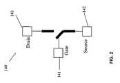
- FIG. 2illustrates a power switch
- FIG. 3illustrates an equivalent circuit of a power switch.
- FIG. 4illustrates an equivalent circuit of a driven power switch.
- FIG. 5illustrates the time dependence of a gate voltage for high and low applied voltages.
- FIGS. 7 a - dillustrate the timing diagrams of voltages and the status of devices in a first time interval.
- FIG. 8illustrates the settings of a power switch driver in a second time interval.
- FIGS. 9 a - dillustrate the timing diagrams of voltages and the status of devices in a second time interval.
- FIG. 10illustrates the settings of a power switch driver in a third time interval.
- FIGS. 11 a - dillustrate the timing diagrams of voltages and the status of devices in a third time interval.
- FIG. 12illustrates the settings of a power switch driver in a fourth time interval.
- FIGS. 13 a - dillustrate the timing diagrams of voltages and the status of devices in a fourth time interval.
- FIG. 14illustrates an embodiment of a power switch driver.
- FIGS. 15 a - jillustrate the timing diagrams of various voltages and the status of various devices in a power switch driver.
- FIG. 16illustrates an embodiment of a pulse width generator.
- FIGS. 17 a - eillustrate the timing diagrams of various voltages and the status of various devices in a pulse width generator.
- FIG. 18illustrates an embodiment of a power switch driver with a track and hold feedback.
- FIG. 19illustrates an embodiment of a track and hold block.
- FIGS. 1-20 of the drawingsLike numerals are used for like and corresponding parts of the various drawings.
- FIG. 1illustrates a power switch driver 100 according to embodiments of the invention.
- Power switch driver 100includes a top driver switch 110 , coupled between a first voltage rail 113 and a driver node 117 .
- Power driveralso includes a bottom driver switch 120 , coupled between driver node 117 and a second voltage rail 122 .
- Power driver 100is also coupled to driver logic 135 , operationally coupled to top driver switch 110 and bottom driver switch 120 .
- Power switch driver 100can drive a power switch 140 .
- FIG. 1illustrates that power switch driver 100 can be connected to power switch 140 by coupling a power switch gate 141 of power switch 140 to driver node 117 and a power switch source 142 to second voltage rail 122 .
- power switch 140can be an n-channel MOSFET, a p-channel MOSFET, a bipolar transistor, or an insulated gate bipolar transistor.
- FIG. 2illustrates a typical structure of power switch 140 .
- Power switch 140includes power switch gate 141 , power switch source 142 , and power switch drain 143 . Voltage applied to power switch gate 141 controls whether current can flow between power switch source 142 and power switch drain 143 , effectively turning power switch 140 on and off.
- FIG. 3illustrates that when power switch gate 141 is closed, an equivalent circuit of power switch 140 includes a gate resistor 146 and a gate capacitor 147 , coupled in series between power switch gate 141 and power switch source 142 .
- FIG. 4illustrates that for the purposes of the outside circuitry the equivalent circuit includes an additional Rd resistor 148 .
- FIG. 5is a plot of the time dependence, or wave form, of the gate voltage Vg(t) of power switch gate 141 for different applied gate voltages Vg 0 .
- Vg(t)is different from Vg 0 because of the voltage drop across Rd resistor 148 when the charging current flows.
- Vg(t)is different from the voltage of gate capacitor 147 because of the voltage drop across gate resistor 146 due to the charging current.
- Vg(t)has this transient curve, because Vg 0 has to charge gate capacitor 147 .
- Embodiments of the inventionresolve this apparent contradiction of design requirements in the following manner.
- Power switch 140is turned on by controlling Vg(t), the gate voltage of power switch gate 141 to a first level Vg 1 , then reduce Vg(t) to a second, lower level Vg 2 , finally turn power switch 140 off by controlling Vg(t) from this second level to a low level, such as the ground.
- FIG. 6illustrates the settings of power driver 100 according to some embodiments, which carry out the first step of the above procedure.
- Top driver switch 110is on and bottom driver switch 120 is turned off.
- FIG. 7 aillustrates that with these settings a gate voltage Vg 0 is applied at time instance t 0 to start the turning on of power switch 140 . This leads to a rising transient gate voltage Vg(t).
- FIGS. 7 b - cillustrate that top driver switch 110 is switched on in this interval (starting at about t 0 ), while bottom driver switch 120 is switched off in the same interval.
- FIG. 7 dillustrates that shortly after t 0 Vg(t) passes the threshold voltage level Vth, turning power switch 140 on. These settings are applied until a time t 1 .
- FIG. 8illustrates the settings of power switch driver 140 after time instance t 1 . After t 1 both top driver switch 110 and bottom driver switch 120 are switched off. This setting cuts off the charging current, which flowed through resistor 148 , gate resistor 146 , and gate capacitor 147 .
- FIGS. 9 a - dillustrate the corresponding timing diagrams.
- FIGS. 9 b - cillustrate that after time instance t 1 both top driver switch 110 and bottom driver switch 120 are turned off.
- FIG. 9 dillustrates that gate voltage Vg(t) is still well above threshold value Vth and thus power switch 140 is still on.
- FIG. 10illustrates that the same settings are maintained for a longer period: again both top driver switch 110 and bottom driver switch 120 remain turned off.
- FIG. 11 aillustrates that after a short time the charging current is essentially stopped by time t 2 and therefore the gate voltage Vg(t) does not change anymore.
- Vg(t)is equal to the voltage of gate capacitor 147 .
- FIGS. 11 b - cillustrate the setting of both top driver switch 110 and bottom driver switch 120 remaining turned off.
- FIG. 11 dillustrates that the voltage level Vg 2 is sufficient to keep power switch 140 turned on.
- FIG. 12illustrates that after a suitably chosen time the settings of power switch 140 are changed at time instance t 3 : while top driver switch 110 is kept turned off, bottom driver switch 120 is turned on. These settings start the discharging of gate capacitor 147 through bottom driver switch 120 .
- FIG. 13 aillustrates that the discharging process causes gate voltage Vg(t) to start decreasing at time instance t 3 from the low value of Vg 2 .
- FIG. 13 billustrates that top driver switch 110 remains turned off.
- FIG. 13 cillustrates that bottom driver 120 was turned at about the time distance t 3 .
- FIG. 13 dillustrates that after the discharcing process started, Vg(t) decays below the threshold voltage Vth, at which point power switch 140 is turned off.
- FIG. 14illustrates an embodiment of driver logic 135 .
- driver logic 135includes a pulse width generator programmer (PWG programmer) 171 and a pulse width generator (PWG) 174 .
- a first input terminal of pulse width generator 174is coupled to pulse width generator programmer 171 .
- a second input terminal of pulse width generator 174is coupled to an input terminal 179 .
- a first output of pulse width generator 174is coupled to a gate of top driver switch 110 .
- Pulse width generator 174is also coupled to second voltage rail 122 , in some embodiments the ground.
- Input terminal 179is also coupled to an inverter 182 , the output of inverter 182 controlling a gate of bottom driver switch 120 .
- FIG. 15illustrates timing diagrams. Only certain diagrams correspond to the just-described embodiment.
- FIG. 15 aillustrates the input signal assuming high and low values in an alternating manner.
- the input signalis periodic, but in others the input signal may vary aperiodically.
- FIG. 15 cillustrates the time dependence of Vg(t) as was discussed in relation to FIGS. 6-13 .
- Vg(t)consists of the rising transient, stopped at t 1 at a level Vg 1 , falling to Vg 2 at time instance t 2 , and staying there until time instance t 3 .
- Vg(t)falls to a low value, such as the ground.
- FIG. 15 eshows that one embodiment of Pulse Width Generator (PWG) Programmer 171 outputs a PWG program voltage, which is inputted into Pulse Width Generator (PWG) 174 .
- the PWG program voltagedetermines the width of the pulses, outputted by PWG 174 .
- FIGS. 15 f - gshows that the output of PWG 174 controls top driver switch 110 .
- top driver switch 110When the PWG voltage is high, top driver switch 110 is turned on, when the PWG voltage is low, top driver switch 110 is turned off.
- FIGS. 15 h - ishow that bottom driver switch 120 is controlled by inverter 182 .
- bottom driver switch 120When the output voltage of inverter 182 is low, bottom driver switch 120 is turned off, when the output voltage of inverter 182 is high, bottom driver switch is turned on.
- FIG. 15 jshows that power switch 140 remains turned on until time instance t 3 , because the time instances (t 0 , t 1 , t 2 and t 3 ) and the corresponding time intervals were selected so that the Vg 2 voltage is higher than Vth. This translates to the requirement that during the initial interval between t 0 and t 1 gate capacitor 146 is charged to a voltage, which is higher than Vth.
- FIG. 16illustrates that in some embodiments Pulse Width Generator 174 includes a comparator 193 .
- the non-inverting input of comparator 193is the first input terminal of PWG 174 , coupled to PWG Programmer 171 . Through this terminal PWG 174 receives a Vctrl PWG program voltage.
- the inverting input of comparator 193is coupled to the output of a ramp generator 191 .
- the input of ramp generator 191is the second input terminal of PWG 174 .
- the output of comparator 193is one of the inputs of an AND gate 197 .
- the other input of AND gate 197is coupled to input terminal 179 .
- FIG. 17illustrates timing diagrams of PWG 174 .
- FIG. 17 aillustrates an input signal, received at input terminal 179 .
- the input signalis periodically changing between high and low values.
- FIG. 17 billustrates that whenever the input signal is high, ramp generator 191 starts generating a steadily rising ramp signal Vramp.
- FIG. 17 cillustrates that in some embodiments PWG Programmer outputs a constant control voltage Vctrl, also referred to as PWG program voltage.
- FIG. 17 dillustrates that the rising ramp voltage Vramp and the constant PWG program voltage are both input into comparator 193 .
- the output of comparator 193is high as long as the ramp voltage is lower that the PWG voltage, but switches to low, when the ramp voltage exceeds the PWG program voltage.
- FIG. 17 eillustrates that, since both the input signal and the output of comparator 193 are input into AND gate 197 , the output of AND gate 197 is high when both the input signal and the comparator output are either high or low.
- FIGS. 15 a through 15 jillustrate, in a new cycle of operation, the PWG program voltage has to be adjusted according to the voltage Vg(t) outputted at driver node 117 in the previous cycle. However, the value of Vg(t) is not available at the time this adjustment needs to be made: Vg(t) already switched off at time instance t 3 .
- FIGS. 15 a through 15 jillustrate timing diagrams of embodiments with a track and hold circuit 201 .
- the previously described timing diagramsare relevant for this embodiment as well.
- FIG. 15 billustrates that in addition the input signal controls whether track and hold circuit 201 should carry out the “track” or the “hold” function.
- track and hold circuit 201tracks the signal sensed at its sensing terminal and outputs it.
- track and hold circuit 201holds the sensed signal it tracked up to that point and keeps outputting the last sensed value.
- FIG. 15illustrate that the described track and hold embodiment indeed holds the last voltage Vg 2 until the next cycle begins. This allows PWG Program block 171 to adjust the PWG program voltage, thus adjusting the width of the outputted pulses to the desired value.
- Sensing terminal 211couples the sensed voltage Vg(t) onto memory capacitor Cmem 221 through switch 218 .
- switch 218When switch 218 is turned on, the voltage of memory capacitor Cmem 221 charges up to Vg(t). Since the inputted voltage Vg(t) is outputted at output terminal 215 , this is called the “tracking” mode. However, when the input signal turns switch 218 off, the charging of memory capacitor is stopped and its voltage remains at the last voltage it was charged to. Since this last voltage keeps being outputted at output terminal 215 , this mode is called “hold”.
- a large number of other track and hold circuitsare known in the art and can be used in the present embodiment.
- Pulse Width Generator 174is modified from its value from PWG Programmer 171 by Error amplifier 204 .
- This implementationcan overcome the variations in the operating conditions mentioned above.
Landscapes
- Electronic Switches (AREA)
- Power Conversion In General (AREA)
Abstract
Description
Claims (19)
Priority Applications (2)
| Application Number | Priority Date | Filing Date | Title |
|---|---|---|---|
| US11/903,338US7551007B2 (en) | 2005-02-11 | 2007-09-21 | Partial switch gate driver |
| US12/489,254US7990187B2 (en) | 2005-02-11 | 2009-06-22 | Partial switch gate driver |
Applications Claiming Priority (2)
| Application Number | Priority Date | Filing Date | Title |
|---|---|---|---|
| US5647905A | 2005-02-11 | 2005-02-11 | |
| US11/903,338US7551007B2 (en) | 2005-02-11 | 2007-09-21 | Partial switch gate driver |
Related Parent Applications (2)
| Application Number | Title | Priority Date | Filing Date |
|---|---|---|---|
| US5647905AContinuation | 2005-02-11 | 2005-02-11 | |
| US11506479Continuation | 2006-08-19 |
Related Child Applications (1)
| Application Number | Title | Priority Date | Filing Date |
|---|---|---|---|
| US12/489,254ContinuationUS7990187B2 (en) | 2005-02-11 | 2009-06-22 | Partial switch gate driver |
Publications (2)
| Publication Number | Publication Date |
|---|---|
| US20080012622A1 US20080012622A1 (en) | 2008-01-17 |
| US7551007B2true US7551007B2 (en) | 2009-06-23 |
Family
ID=38948664
Family Applications (2)
| Application Number | Title | Priority Date | Filing Date |
|---|---|---|---|
| US11/903,338Expired - LifetimeUS7551007B2 (en) | 2005-02-11 | 2007-09-21 | Partial switch gate driver |
| US12/489,254Expired - LifetimeUS7990187B2 (en) | 2005-02-11 | 2009-06-22 | Partial switch gate driver |
Family Applications After (1)
| Application Number | Title | Priority Date | Filing Date |
|---|---|---|---|
| US12/489,254Expired - LifetimeUS7990187B2 (en) | 2005-02-11 | 2009-06-22 | Partial switch gate driver |
Country Status (1)
| Country | Link |
|---|---|
| US (2) | US7551007B2 (en) |
Cited By (3)
| Publication number | Priority date | Publication date | Assignee | Title |
|---|---|---|---|---|
| US20090315593A1 (en)* | 2005-02-11 | 2009-12-24 | Sidley Austin Llp | Partial Switch Gate Driver |
| US20120049811A1 (en)* | 2010-08-31 | 2012-03-01 | Fujitsu Semiconductor Limited | Output switching circuit |
| DE102013217902A1 (en)* | 2013-09-08 | 2015-03-12 | Rwth Aachen | Driver arrangement for a transistor to be controlled |
Families Citing this family (2)
| Publication number | Priority date | Publication date | Assignee | Title |
|---|---|---|---|---|
| US9025294B2 (en)* | 2012-02-24 | 2015-05-05 | Hamilton Sundstrand Corporation | System and method for controlling solid state circuit breakers |
| DE102012015787B3 (en) | 2012-08-08 | 2013-12-12 | Fairchild Semiconductor Corp. | Gate driver for driving gate of switch, has control input for receiving control signal, where amplified output signal is provided by output for controlling gate of switch, while control device is connected between control input and output |
Citations (19)
| Publication number | Priority date | Publication date | Assignee | Title |
|---|---|---|---|---|
| US4065678A (en)* | 1976-07-02 | 1977-12-27 | Motorola, Inc. | Clamped push-pull driver circuit with output feedback |
| US4972130A (en) | 1988-11-16 | 1990-11-20 | Sgs-Thomson Microelectronics, S.R.L. | Multipurpose, internally configurable integrated circuit for driving in a switching mode external inductive loads according to a selectable connection scheme |
| US5099138A (en)* | 1989-11-22 | 1992-03-24 | Mitsubishi Denki Kabushiki Kaisha | Switching device driving circuit |
| US5343084A (en)* | 1991-04-30 | 1994-08-30 | Sgs-Thomson Microelectronics S.A. | Variable level periodic excitation circuit for a capacitive load |
| US5631588A (en)* | 1994-03-29 | 1997-05-20 | Sgs-Thomson Microelectronics, S.R.L. | Power output stage with limited current absorption during high-impedance phase |
| US5729165A (en) | 1996-04-04 | 1998-03-17 | National Science Council | 1.5v full-swing bootstrapped CMOS large capacitive-load driver circuit suitable for low-voltage deep-submicron CMOS VLSI |
| US5760620A (en) | 1996-04-22 | 1998-06-02 | Quantum Effect Design, Inc. | CMOS limited-voltage-swing clock driver for reduced power driving high-frequency clocks |
| US6018256A (en)* | 1995-07-07 | 2000-01-25 | Seiko Epson Corporation | Output circuit and electronic apparatus using the same |
| US6094079A (en) | 1998-12-21 | 2000-07-25 | Caterpillar Inc. | Sequencer module for a pulse width modulation driver |
| US6359478B1 (en) | 2001-08-31 | 2002-03-19 | Pericom Semiconductor Corp. | Reduced-undershoot CMOS output buffer with delayed VOL-driver transistor |
| US6535035B2 (en) | 2000-11-17 | 2003-03-18 | Texas Instruments Incorporated | Driver and method for switching applications |
| US6552583B1 (en) | 2001-10-11 | 2003-04-22 | Pericom Semiconductor Corp. | ESD-protection device with active R-C coupling to gate of large output transistor |
| US6897683B2 (en) | 2002-11-14 | 2005-05-24 | Fyre Storm, Inc. | Driver including first and second buffers for driving an external coil or first and second transistors |
| US6977533B2 (en)* | 2003-04-17 | 2005-12-20 | Dialog Semiconductor Gmbh | 32V H-bridge driver with CMOS circuits |
| US7038524B2 (en) | 2003-05-16 | 2006-05-02 | Power Integrations, Inc. | Method and apparatus for extending the size of a transistor beyond one integrated circuit |
| US7046050B1 (en) | 2004-01-02 | 2006-05-16 | Sauer-Danfoss Inc. | High side NFET gate driving circuit |
| US7071740B2 (en)* | 2003-12-30 | 2006-07-04 | Texas Instruments Incorporated | Current limiting circuit for high-speed low-side driver outputs |
| US7088151B1 (en) | 2004-04-21 | 2006-08-08 | Intersil Americas Inc. | High voltage gate driver using a low voltage multi-level current pulse translator |
| US7091752B2 (en) | 2003-09-30 | 2006-08-15 | Power Integrations, Inc. | Method and apparatus for simplifying the control of a switch |
Family Cites Families (1)
| Publication number | Priority date | Publication date | Assignee | Title |
|---|---|---|---|---|
| US7551007B2 (en)* | 2005-02-11 | 2009-06-23 | Fairchild Semiconductor Corporation | Partial switch gate driver |
- 2007
- 2007-09-21USUS11/903,338patent/US7551007B2/ennot_activeExpired - Lifetime
- 2009
- 2009-06-22USUS12/489,254patent/US7990187B2/ennot_activeExpired - Lifetime
Patent Citations (19)
| Publication number | Priority date | Publication date | Assignee | Title |
|---|---|---|---|---|
| US4065678A (en)* | 1976-07-02 | 1977-12-27 | Motorola, Inc. | Clamped push-pull driver circuit with output feedback |
| US4972130A (en) | 1988-11-16 | 1990-11-20 | Sgs-Thomson Microelectronics, S.R.L. | Multipurpose, internally configurable integrated circuit for driving in a switching mode external inductive loads according to a selectable connection scheme |
| US5099138A (en)* | 1989-11-22 | 1992-03-24 | Mitsubishi Denki Kabushiki Kaisha | Switching device driving circuit |
| US5343084A (en)* | 1991-04-30 | 1994-08-30 | Sgs-Thomson Microelectronics S.A. | Variable level periodic excitation circuit for a capacitive load |
| US5631588A (en)* | 1994-03-29 | 1997-05-20 | Sgs-Thomson Microelectronics, S.R.L. | Power output stage with limited current absorption during high-impedance phase |
| US6018256A (en)* | 1995-07-07 | 2000-01-25 | Seiko Epson Corporation | Output circuit and electronic apparatus using the same |
| US5729165A (en) | 1996-04-04 | 1998-03-17 | National Science Council | 1.5v full-swing bootstrapped CMOS large capacitive-load driver circuit suitable for low-voltage deep-submicron CMOS VLSI |
| US5760620A (en) | 1996-04-22 | 1998-06-02 | Quantum Effect Design, Inc. | CMOS limited-voltage-swing clock driver for reduced power driving high-frequency clocks |
| US6094079A (en) | 1998-12-21 | 2000-07-25 | Caterpillar Inc. | Sequencer module for a pulse width modulation driver |
| US6535035B2 (en) | 2000-11-17 | 2003-03-18 | Texas Instruments Incorporated | Driver and method for switching applications |
| US6359478B1 (en) | 2001-08-31 | 2002-03-19 | Pericom Semiconductor Corp. | Reduced-undershoot CMOS output buffer with delayed VOL-driver transistor |
| US6552583B1 (en) | 2001-10-11 | 2003-04-22 | Pericom Semiconductor Corp. | ESD-protection device with active R-C coupling to gate of large output transistor |
| US6897683B2 (en) | 2002-11-14 | 2005-05-24 | Fyre Storm, Inc. | Driver including first and second buffers for driving an external coil or first and second transistors |
| US6977533B2 (en)* | 2003-04-17 | 2005-12-20 | Dialog Semiconductor Gmbh | 32V H-bridge driver with CMOS circuits |
| US7038524B2 (en) | 2003-05-16 | 2006-05-02 | Power Integrations, Inc. | Method and apparatus for extending the size of a transistor beyond one integrated circuit |
| US7091752B2 (en) | 2003-09-30 | 2006-08-15 | Power Integrations, Inc. | Method and apparatus for simplifying the control of a switch |
| US7071740B2 (en)* | 2003-12-30 | 2006-07-04 | Texas Instruments Incorporated | Current limiting circuit for high-speed low-side driver outputs |
| US7046050B1 (en) | 2004-01-02 | 2006-05-16 | Sauer-Danfoss Inc. | High side NFET gate driving circuit |
| US7088151B1 (en) | 2004-04-21 | 2006-08-08 | Intersil Americas Inc. | High voltage gate driver using a low voltage multi-level current pulse translator |
Cited By (8)
| Publication number | Priority date | Publication date | Assignee | Title |
|---|---|---|---|---|
| US20090315593A1 (en)* | 2005-02-11 | 2009-12-24 | Sidley Austin Llp | Partial Switch Gate Driver |
| US7990187B2 (en)* | 2005-02-11 | 2011-08-02 | Fairchild Semiconductor Corporation | Partial switch gate driver |
| US20120049811A1 (en)* | 2010-08-31 | 2012-03-01 | Fujitsu Semiconductor Limited | Output switching circuit |
| CN102386901A (en)* | 2010-08-31 | 2012-03-21 | 富士通半导体股份有限公司 | Output switching circuit |
| US8957648B2 (en)* | 2010-08-31 | 2015-02-17 | Spansion Llc | Output switching circuit |
| CN102386901B (en)* | 2010-08-31 | 2015-04-22 | 斯班逊有限公司 | Output switching circuit |
| US9502979B2 (en) | 2010-08-31 | 2016-11-22 | Cypress Semiconductor Corporation | Output switching circuit |
| DE102013217902A1 (en)* | 2013-09-08 | 2015-03-12 | Rwth Aachen | Driver arrangement for a transistor to be controlled |
Also Published As
| Publication number | Publication date |
|---|---|
| US20080012622A1 (en) | 2008-01-17 |
| US7990187B2 (en) | 2011-08-02 |
| US20090315593A1 (en) | 2009-12-24 |
Similar Documents
| Publication | Publication Date | Title |
|---|---|---|
| US8222879B2 (en) | Method and apparatus for synchronous buck with active negative current modulation | |
| US10283994B2 (en) | Switching charging circuit | |
| US6222403B1 (en) | Slew rate output circuit with an improved driving capability of driving an output MOS field effect transistor | |
| TWI394024B (en) | Power supply controller and method therefor | |
| TWI418128B (en) | Voltage regulator and method for forming a switched capacitor controller | |
| US20060034114A1 (en) | Gate driving circuit and gate driving method of power MOSFET | |
| US7990187B2 (en) | Partial switch gate driver | |
| US10110125B2 (en) | System and method of driving a switch circuit | |
| JP6436230B2 (en) | Driving circuit | |
| US7880458B2 (en) | Method and device for driving power converters | |
| US7667524B2 (en) | Driver circuit and method with reduced DI/DT and having delay compensation | |
| JP2020127145A (en) | Bridge output circuit, power supply device, and semiconductor device | |
| KR20100056244A (en) | Switch driving circuit and switch driving method | |
| JPH11197602A (en) | Piezo drive circuit | |
| WO2022050032A1 (en) | Gate drive device and load supply circuit | |
| US12101083B2 (en) | High speed driver for high frequency DCDC converter | |
| US7205751B2 (en) | Enable and disable of diode emulation in a DC/DC converter | |
| US11888394B2 (en) | High-efficiency pulse width modulation for switching power converters | |
| JP3608472B2 (en) | Output circuit | |
| JP2018207276A (en) | Gate drive circuit | |
| JP2024140966A (en) | Motor driver circuit | |
| US7236021B2 (en) | Method of controlling slope and dead time in an integrated output buffer with inductive load | |
| JP2001008494A (en) | Bridge power converter circuit | |
| US6275019B1 (en) | Absolute control of non overlap time in switch mode power controller output stages | |
| US11569809B2 (en) | Load drive control device |
Legal Events
| Date | Code | Title | Description |
|---|---|---|---|
| STCF | Information on status: patent grant | Free format text:PATENTED CASE | |
| FPAY | Fee payment | Year of fee payment:4 | |
| FEPP | Fee payment procedure | Free format text:PAYOR NUMBER ASSIGNED (ORIGINAL EVENT CODE: ASPN); ENTITY STATUS OF PATENT OWNER: LARGE ENTITY | |
| AS | Assignment | Owner name:FAIRCHILD SEMICONDUCTOR CORPORATION, CALIFORNIA Free format text:ASSIGNMENT OF ASSIGNORS INTEREST;ASSIGNORS:KHASIEV, VICTOR;BERTHIAUME, RONALD;REEL/FRAME:039268/0948 Effective date:20070921 | |
| AS | Assignment | Owner name:DEUTSCHE BANK AG NEW YORK BRANCH, AS COLLATERAL AGENT, NEW YORK Free format text:PATENT SECURITY AGREEMENT;ASSIGNOR:FAIRCHILD SEMICONDUCTOR CORPORATION;REEL/FRAME:040075/0644 Effective date:20160916 Owner name:DEUTSCHE BANK AG NEW YORK BRANCH, AS COLLATERAL AG Free format text:PATENT SECURITY AGREEMENT;ASSIGNOR:FAIRCHILD SEMICONDUCTOR CORPORATION;REEL/FRAME:040075/0644 Effective date:20160916 | |
| FPAY | Fee payment | Year of fee payment:8 | |
| MAFP | Maintenance fee payment | Free format text:PAYMENT OF MAINTENANCE FEE, 12TH YEAR, LARGE ENTITY (ORIGINAL EVENT CODE: M1553); ENTITY STATUS OF PATENT OWNER: LARGE ENTITY Year of fee payment:12 | |
| AS | Assignment | Owner name:SEMICONDUCTOR COMPONENTS INDUSTRIES, LLC, ARIZONA Free format text:ASSIGNMENT OF ASSIGNORS INTEREST;ASSIGNOR:FAIRCHILD SEMICONDUCTOR CORPORATION;REEL/FRAME:057694/0374 Effective date:20210722 | |
| AS | Assignment | Owner name:FAIRCHILD SEMICONDUCTOR CORPORATION, ARIZONA Free format text:RELEASE BY SECURED PARTY;ASSIGNOR:DEUTSCHE BANK AG NEW YORK BRANCH;REEL/FRAME:057969/0206 Effective date:20211027 | |
| AS | Assignment | Owner name:DEUTSCHE BANK AG NEW YORK BRANCH, AS COLLATERAL AGENT, NEW YORK Free format text:SECURITY INTEREST;ASSIGNOR:SEMICONDUCTOR COMPONENTS INDUSTRIES, LLC;REEL/FRAME:058871/0799 Effective date:20211028 | |
| AS | Assignment | Owner name:FAIRCHILD SEMICONDUCTOR CORPORATION, ARIZONA Free format text:RELEASE OF SECURITY INTEREST IN PATENTS RECORDED AT REEL 040075, FRAME 0644;ASSIGNOR:DEUTSCHE BANK AG NEW YORK BRANCH, AS COLLATERAL AGENT;REEL/FRAME:064070/0536 Effective date:20230622 Owner name:SEMICONDUCTOR COMPONENTS INDUSTRIES, LLC, ARIZONA Free format text:RELEASE OF SECURITY INTEREST IN PATENTS RECORDED AT REEL 040075, FRAME 0644;ASSIGNOR:DEUTSCHE BANK AG NEW YORK BRANCH, AS COLLATERAL AGENT;REEL/FRAME:064070/0536 Effective date:20230622 | |
| AS | Assignment | Owner name:FAIRCHILD SEMICONDUCTOR CORPORATION, ARIZONA Free format text:RELEASE OF SECURITY INTEREST IN PATENTS RECORDED AT REEL 058871, FRAME 0799;ASSIGNOR:DEUTSCHE BANK AG NEW YORK BRANCH, AS COLLATERAL AGENT;REEL/FRAME:065653/0001 Effective date:20230622 Owner name:SEMICONDUCTOR COMPONENTS INDUSTRIES, LLC, ARIZONA Free format text:RELEASE OF SECURITY INTEREST IN PATENTS RECORDED AT REEL 058871, FRAME 0799;ASSIGNOR:DEUTSCHE BANK AG NEW YORK BRANCH, AS COLLATERAL AGENT;REEL/FRAME:065653/0001 Effective date:20230622 |