US7550395B2 - Control of photoelectrochemical (PEC) etching by modification of the local electrochemical potential of the semiconductor structure relative to the electrolyte - Google Patents
Control of photoelectrochemical (PEC) etching by modification of the local electrochemical potential of the semiconductor structure relative to the electrolyteDownload PDFInfo
- Publication number
- US7550395B2 US7550395B2US11/263,314US26331405AUS7550395B2US 7550395 B2US7550395 B2US 7550395B2US 26331405 AUS26331405 AUS 26331405AUS 7550395 B2US7550395 B2US 7550395B2
- Authority
- US
- United States
- Prior art keywords
- layers
- etching
- etch
- photo
- semiconductor structure
- Prior art date
- Legal status (The legal status is an assumption and is not a legal conclusion. Google has not performed a legal analysis and makes no representation as to the accuracy of the status listed.)
- Active - Reinstated, expires
Links
- 238000005530etchingMethods0.000titleclaimsabstractdescription68
- 239000004065semiconductorSubstances0.000titleclaimsabstractdescription46
- 239000003792electrolyteSubstances0.000titleclaimsdescription18
- 238000012986modificationMethods0.000titledescription10
- 230000004048modificationEffects0.000titledescription10
- 238000000034methodMethods0.000claimsabstractdescription37
- 239000000463materialSubstances0.000claimsdescription46
- 150000004767nitridesChemical class0.000claimsdescription18
- 239000008151electrolyte solutionSubstances0.000claimsdescription6
- 238000000605extractionMethods0.000claimsdescription3
- 230000001737promoting effectEffects0.000claims1
- 238000004519manufacturing processMethods0.000description14
- 230000003287optical effectEffects0.000description11
- 230000008569processEffects0.000description11
- 239000000758substrateSubstances0.000description11
- 229910002601GaNInorganic materials0.000description10
- 239000000969carrierSubstances0.000description7
- 239000012528membraneSubstances0.000description7
- 229920002120photoresistant polymerPolymers0.000description7
- 238000005286illuminationMethods0.000description6
- 239000000203mixtureSubstances0.000description6
- 230000008901benefitEffects0.000description5
- 239000002019doping agentSubstances0.000description4
- 238000000151depositionMethods0.000description3
- 230000008021depositionEffects0.000description3
- 238000013461designMethods0.000description3
- 229910052751metalInorganic materials0.000description3
- 239000002184metalSubstances0.000description3
- 239000004038photonic crystalSubstances0.000description3
- 238000001020plasma etchingMethods0.000description3
- 229910052594sapphireInorganic materials0.000description3
- 239000010980sapphireSubstances0.000description3
- HBMJWWWQQXIZIP-UHFFFAOYSA-Nsilicon carbideChemical compound[Si+]#[C-]HBMJWWWQQXIZIP-UHFFFAOYSA-N0.000description3
- ZAMOUSCENKQFHK-UHFFFAOYSA-NChlorine atomChemical compound[Cl]ZAMOUSCENKQFHK-UHFFFAOYSA-N0.000description2
- 238000010521absorption reactionMethods0.000description2
- 239000010406cathode materialSubstances0.000description2
- 238000006243chemical reactionMethods0.000description2
- 229910052801chlorineInorganic materials0.000description2
- 239000000460chlorineSubstances0.000description2
- 239000004020conductorSubstances0.000description2
- 230000007547defectEffects0.000description2
- 230000001419dependent effectEffects0.000description2
- 238000010586diagramMethods0.000description2
- 238000009792diffusion processMethods0.000description2
- 238000005566electron beam evaporationMethods0.000description2
- 238000002248hydride vapour-phase epitaxyMethods0.000description2
- 238000009616inductively coupled plasmaMethods0.000description2
- 238000005468ion implantationMethods0.000description2
- 230000005693optoelectronicsEffects0.000description2
- 238000000103photoluminescence spectrumMethods0.000description2
- 230000006798recombinationEffects0.000description2
- 238000005215recombinationMethods0.000description2
- 238000002310reflectometryMethods0.000description2
- 238000001878scanning electron micrographMethods0.000description2
- 229910010271silicon carbideInorganic materials0.000description2
- 238000012546transferMethods0.000description2
- 208000012868OvergrowthDiseases0.000description1
- 239000002253acidSubstances0.000description1
- 230000002378acidificating effectEffects0.000description1
- 150000007513acidsChemical class0.000description1
- 229910045601alloyInorganic materials0.000description1
- 239000000956alloySubstances0.000description1
- 238000013459approachMethods0.000description1
- 239000007864aqueous solutionSubstances0.000description1
- 239000003638chemical reducing agentSubstances0.000description1
- 238000005229chemical vapour depositionMethods0.000description1
- 230000001427coherent effectEffects0.000description1
- 238000011161developmentMethods0.000description1
- 238000001312dry etchingMethods0.000description1
- 238000003487electrochemical reactionMethods0.000description1
- 239000012776electronic materialSubstances0.000description1
- 238000005516engineering processMethods0.000description1
- 239000007789gasSubstances0.000description1
- 238000010884ion-beam techniqueMethods0.000description1
- 150000002500ionsChemical class0.000description1
- 230000000873masking effectEffects0.000description1
- 238000005259measurementMethods0.000description1
- 230000007246mechanismEffects0.000description1
- 229910044991metal oxideInorganic materials0.000description1
- 150000002739metalsChemical class0.000description1
- 238000001451molecular beam epitaxyMethods0.000description1
- 239000007800oxidant agentSubstances0.000description1
- 230000001590oxidative effectEffects0.000description1
- TWNQGVIAIRXVLR-UHFFFAOYSA-Noxo(oxoalumanyloxy)alumaneChemical compoundO=[Al]O[Al]=OTWNQGVIAIRXVLR-UHFFFAOYSA-N0.000description1
- 239000012071phaseSubstances0.000description1
- 238000005498polishingMethods0.000description1
- 239000002243precursorSubstances0.000description1
- 239000000243solutionSubstances0.000description1
- 238000003892spreadingMethods0.000description1
- 230000007480spreadingEffects0.000description1
- 238000003631wet chemical etchingMethods0.000description1
- 238000009736wettingMethods0.000description1
Images


Classifications
- H—ELECTRICITY
- H01—ELECTRIC ELEMENTS
- H01L—SEMICONDUCTOR DEVICES NOT COVERED BY CLASS H10
- H01L21/00—Processes or apparatus adapted for the manufacture or treatment of semiconductor or solid state devices or of parts thereof
- H01L21/02—Manufacture or treatment of semiconductor devices or of parts thereof
- H01L21/04—Manufacture or treatment of semiconductor devices or of parts thereof the devices having potential barriers, e.g. a PN junction, depletion layer or carrier concentration layer
- H01L21/18—Manufacture or treatment of semiconductor devices or of parts thereof the devices having potential barriers, e.g. a PN junction, depletion layer or carrier concentration layer the devices having semiconductor bodies comprising elements of Group IV of the Periodic Table or AIIIBV compounds with or without impurities, e.g. doping materials
- H01L21/30—Treatment of semiconductor bodies using processes or apparatus not provided for in groups H01L21/20 - H01L21/26
- H01L21/302—Treatment of semiconductor bodies using processes or apparatus not provided for in groups H01L21/20 - H01L21/26 to change their surface-physical characteristics or shape, e.g. etching, polishing, cutting
- H01L21/306—Chemical or electrical treatment, e.g. electrolytic etching
- H01L21/3063—Electrolytic etching
- H01L21/30635—Electrolytic etching of AIIIBV compounds
- B—PERFORMING OPERATIONS; TRANSPORTING
- B82—NANOTECHNOLOGY
- B82Y—SPECIFIC USES OR APPLICATIONS OF NANOSTRUCTURES; MEASUREMENT OR ANALYSIS OF NANOSTRUCTURES; MANUFACTURE OR TREATMENT OF NANOSTRUCTURES
- B82Y20/00—Nanooptics, e.g. quantum optics or photonic crystals
- H—ELECTRICITY
- H01—ELECTRIC ELEMENTS
- H01S—DEVICES USING THE PROCESS OF LIGHT AMPLIFICATION BY STIMULATED EMISSION OF RADIATION [LASER] TO AMPLIFY OR GENERATE LIGHT; DEVICES USING STIMULATED EMISSION OF ELECTROMAGNETIC RADIATION IN WAVE RANGES OTHER THAN OPTICAL
- H01S5/00—Semiconductor lasers
- H01S5/10—Construction or shape of the optical resonator, e.g. extended or external cavity, coupled cavities, bent-guide, varying width, thickness or composition of the active region
- H01S5/1071—Ring-lasers
- H01S5/1075—Disk lasers with special modes, e.g. whispering gallery lasers
- H—ELECTRICITY
- H01—ELECTRIC ELEMENTS
- H01S—DEVICES USING THE PROCESS OF LIGHT AMPLIFICATION BY STIMULATED EMISSION OF RADIATION [LASER] TO AMPLIFY OR GENERATE LIGHT; DEVICES USING STIMULATED EMISSION OF ELECTROMAGNETIC RADIATION IN WAVE RANGES OTHER THAN OPTICAL
- H01S2304/00—Special growth methods for semiconductor lasers
- H01S2304/12—Pendeo epitaxial lateral overgrowth [ELOG], e.g. for growing GaN based blue laser diodes
- H—ELECTRICITY
- H01—ELECTRIC ELEMENTS
- H01S—DEVICES USING THE PROCESS OF LIGHT AMPLIFICATION BY STIMULATED EMISSION OF RADIATION [LASER] TO AMPLIFY OR GENERATE LIGHT; DEVICES USING STIMULATED EMISSION OF ELECTROMAGNETIC RADIATION IN WAVE RANGES OTHER THAN OPTICAL
- H01S5/00—Semiconductor lasers
- H01S5/10—Construction or shape of the optical resonator, e.g. extended or external cavity, coupled cavities, bent-guide, varying width, thickness or composition of the active region
- H01S5/18—Surface-emitting [SE] lasers, e.g. having both horizontal and vertical cavities
- H01S5/183—Surface-emitting [SE] lasers, e.g. having both horizontal and vertical cavities having only vertical cavities, e.g. vertical cavity surface-emitting lasers [VCSEL]
- H01S5/18308—Surface-emitting [SE] lasers, e.g. having both horizontal and vertical cavities having only vertical cavities, e.g. vertical cavity surface-emitting lasers [VCSEL] having a special structure for lateral current or light confinement
- H01S5/18316—Airgap confined
- H—ELECTRICITY
- H01—ELECTRIC ELEMENTS
- H01S—DEVICES USING THE PROCESS OF LIGHT AMPLIFICATION BY STIMULATED EMISSION OF RADIATION [LASER] TO AMPLIFY OR GENERATE LIGHT; DEVICES USING STIMULATED EMISSION OF ELECTROMAGNETIC RADIATION IN WAVE RANGES OTHER THAN OPTICAL
- H01S5/00—Semiconductor lasers
- H01S5/20—Structure or shape of the semiconductor body to guide the optical wave ; Confining structures perpendicular to the optical axis, e.g. index or gain guiding, stripe geometry, broad area lasers, gain tailoring, transverse or lateral reflectors, special cladding structures, MQW barrier reflection layers
- H01S5/2054—Methods of obtaining the confinement
- H01S5/2081—Methods of obtaining the confinement using special etching techniques
- H—ELECTRICITY
- H01—ELECTRIC ELEMENTS
- H01S—DEVICES USING THE PROCESS OF LIGHT AMPLIFICATION BY STIMULATED EMISSION OF RADIATION [LASER] TO AMPLIFY OR GENERATE LIGHT; DEVICES USING STIMULATED EMISSION OF ELECTROMAGNETIC RADIATION IN WAVE RANGES OTHER THAN OPTICAL
- H01S5/00—Semiconductor lasers
- H01S5/30—Structure or shape of the active region; Materials used for the active region
- H01S5/34—Structure or shape of the active region; Materials used for the active region comprising quantum well or superlattice structures, e.g. single quantum well [SQW] lasers, multiple quantum well [MQW] lasers or graded index separate confinement heterostructure [GRINSCH] lasers
- H01S5/343—Structure or shape of the active region; Materials used for the active region comprising quantum well or superlattice structures, e.g. single quantum well [SQW] lasers, multiple quantum well [MQW] lasers or graded index separate confinement heterostructure [GRINSCH] lasers in AIIIBV compounds, e.g. AlGaAs-laser, InP-based laser
- H01S5/34333—Structure or shape of the active region; Materials used for the active region comprising quantum well or superlattice structures, e.g. single quantum well [SQW] lasers, multiple quantum well [MQW] lasers or graded index separate confinement heterostructure [GRINSCH] lasers in AIIIBV compounds, e.g. AlGaAs-laser, InP-based laser with a well layer based on Ga(In)N or Ga(In)P, e.g. blue laser
- H—ELECTRICITY
- H10—SEMICONDUCTOR DEVICES; ELECTRIC SOLID-STATE DEVICES NOT OTHERWISE PROVIDED FOR
- H10H—INORGANIC LIGHT-EMITTING SEMICONDUCTOR DEVICES HAVING POTENTIAL BARRIERS
- H10H20/00—Individual inorganic light-emitting semiconductor devices having potential barriers, e.g. light-emitting diodes [LED]
- H10H20/80—Constructional details
- H10H20/81—Bodies
- H10H20/814—Bodies having reflecting means, e.g. semiconductor Bragg reflectors
Definitions
- the present inventionrelates to the control of photoelectrochemical (PEC) etching by modification of the local electrochemical potential of the semiconductor structure relative to the electrolyte.
- PECphotoelectrochemical
- PEC etchinguses above-bandgap illumination to generate carriers (specifically holes) needed to etch III-nitrides.
- the electrochemical potential of the semiconductor material surface relative to the electrolytecauses holes to be drawn toward the semiconductor-electrolyte interface in n-type (unintentionally-doped or doped) material, allowing them to participate in the electrochemical reactions necessary for material removal.
- the etching mechanismrelies heavily on the absorption of incident light and the electrochemical potential of the semiconductor material relative to the electrolyte, PEC etching can be defect-selective, dopant-selective, and bandgap-selective.
- the placement of suitable layers within the semiconductor structuremay be used to prevent etching of specific layers. Additionally, the placement of a cathode in contact with a particular layer (or layers) of a semiconductor structure may be used to promote etching of a specific layer (or layers) when desired. A combination of these two approaches may be used, as required for certain applications.
- DBRdistributed Bragg reflector
- This inventionalso allows for significant improvements over existing practices in the following nitride-based applications:
- Substrate removal and cavity thinningCurrently, the commonly used methods include laser-assisted debonding [13, 14] and inductively coupled plasma (ICP) etching [15-17] or polishing, respectively. These methods are cumbersome, and typically result in relatively imprecise material thicknesses.
- ICPinductively coupled plasma
- This inventiondescribes a scheme for fabricating III-nitride semiconductor structures wherein a highly selective photo-induced etch is achieved through strategic modification of the local electrochemical potential of the semiconductor structure relative to the electrolyte. This is accomplished through:
- the use of a suitable light source during PEC etchingwhich enables the photo-generation of electrons and holes in layers with bandgap energies lower than the energy of the incident light.
- the etchwill not proceed without photo-induced carriers.
- the light sourcemay be a laser or a broad-spectrum source with/without a filter.
- PEC etchingis a photo-induced etch process in which only layers that contain photo-generated carriers may be susceptible to etching. Although several reports exist of etching induced by the photoelectrochemical process, specific descriptions of local control of the etch process through modifications of the electrochemical component of the etching have not been provided. In general, control of the PEC etch process can be achieved through variation of wavelength, duration, and intensity of the incident illumination, composition and concentration of the electrolyte and strategic modification of the electrical potential of the structure relative to the electrolyte.
- This inventiondescribes a method to locally control the electrical potential of a structure or device (and hence locally control lateral and/or vertical PEC etch rates) by appropriate placement of electrically resistive layers or layers that impede electron flow within the semiconductor structure, and/or by positioning the cathode in contact with specific layers of the semiconductor structure during PEC etching.
- This inventionmay thus be used to our advantage to fabricate several structures of interest, including but not limited to microdisk resonators, air-gap DBRs, semiconductor membranes, and electrical and optical apertures, as well as for specific techniques of interest, including but not limited to substrate removal.
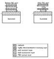
- FIGS. 1-8illustrate several example structures and their resulting etch profiles in cross-sectional schematic views
- FIG. 9is a schematic of the PEC etch set-up and includes two band diagrams illustrating the general principles of PEC etching (doping-selective and bandgap-selective);
- FIGS. 10( a )-( e )are cross-sectional schematics for each fabrication step used to make a microdisk
- FIG. 11is a scanning electron micrograph of the final microdisk structure
- FIG. 12includes photoluminescence spectra of unprocessed material and a 3.5 micron diameter microdisk
- FIGS. 13( a )-( e )are cross-sectional schematics for each fabrication step used to make a vertically oriented DBR.
- FIG. 14is a scanning electron microscope (SEM) image of the final DBR structure.
- PEC etchingis a viable method for producing specific geometries in the III-nitride material system, forming three-dimensional structures that would be extremely challenging to produce with gas-phase etching processes or more standard wet chemical etching.
- the existence of a controlled three-dimensional etch processcan give rise to numerous useful device geometries.
- an undercut geometryis desirable in several applications including but not limited to microdisk resonators, air-gap DBRs, semiconductor membranes and cantilevers, electrical and optical apertures, and in substrate removal.
- Microdisk resonatorstypically show high-quality optical modes, and reduced optical and electrical lasing thresholds.
- the invention described hereinprovides a method for fabricating high-quality, “mushroom-shaped” microdisk resonators in the nitride semiconductor system.
- Air-gap DBRshave several advantages over typical epitaxial or dielectric DBRs, including wider stopbands, higher reflectivity values per DBR period, and lower effective cavity lengths. They may be used as high-reflectivity mirrors in vertical cavity surface emitting lasers (VCSELs) and resonant cavity light emitting diodes (LEDs). This invention facilitates the fabrication of high-quality air-gap DBR structures in the nitride semiconductor system.
- VCSELsvertical cavity surface emitting lasers
- LEDsresonant cavity light emitting diodes
- Semiconductor membranesare frequently used for a variety of applications including MEMS and photonic crystals.
- the nitridesoffer unique optical and electrical material properties which are well suited for these applications.
- This inventionenables the fabrication of membrane devices in the nitride material system.
- Aperturesare commonly used in several optoelectronic and electronic devices to reduce current spreading and to achieve better optical confinement. This invention may be used to effectively achieve apertures in the nitride semiconductor system.
- Certain applicationssuch as high-power LEDs require the removal of the substrate for improved heat extraction.
- This inventionnot only makes substrate removal possible, but also allows for precise thickness control of the sub-mounted structure such as in a microcavity LED.
- This inventionmay therefore find application in practically all nitride-based electronic and optical devices.
- This disclosuredescribes a method of locally controlling the etch rate and etch susceptibility of a semiconductor layer by manipulating photo-induced carrier dynamics within the layer through selective cathode placement relative to the layer and/or by incorporating highly resistive or electron-blocking layers into the semiconductor multilayer structure.
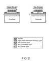
- the etch selectivity described aboveis achieved through appropriate choice of the following design elements. It is implicit that under the conditions considered, PEC etching is strictly a light-induced process. In the absence of light, no etching occurs in any of the layers.
- Light sourceThis can be any light source (coherent or incoherent), filtered or unfiltered, which emits photons with energy greater than the bandgap energy of the “PEC etched” or “etch-susceptible” layers under the conditions considered.
- PEC etched layerThis is a material layer which has a bandgap smaller than the energy of the incident light, is either n-type or unintentionally-doped, and which also has access to a conductive path for electrons, such that the photo-generated electrons can be collected before they recombine with the photo-generated holes, thereby allowing PEC etching to proceed in this layer under the conditions considered.
- Etch-susceptible layerThis is a material layer which has a bandgap smaller than the energy of the incident light and is either n-type or unintentionally-doped, but does not have access to a conductive path for electrons, such that the photo-generated electrons and holes recombine before etching can occur under the conditions considered.
- Etch-resistant layerThis is an electrically conductive material layer that either has a bandgap larger than the energy of the incident light or is p-type, such that is not etched under the conditions considered.
- Highly resistive/electron-blocking layerThis is an electrically resistive material layer that either has a bandgap larger than the energy of the incident light or is p-type, such that is not etched under the conditions considered. Such a layer impedes the extraction of electrons from the “etch-susceptible” layers, thereby altering the carrier dynamics in the “etch-susceptible” layers to inhibit etching under the conditions considered.
- CathodeThis is any highly conductive material that can be used to allow electrons to interact readily with the electrolyte under the conditions considered.
- ElectrolyteThis is an acidic or basic aqueous solution of the appropriate chemistry and concentration, which allows the appropriate reactions necessary for etching to occur in only the “PEC etched” layer, but has reaction rates slow enough to allow photo-generated electron-hole recombination to dominate in the “etch-susceptible” layer so as to reduce or prevent etching in this type of layer under the conditions considered.
- the substrate for the semiconductor layer depositioncan be any material compatible with the growth technique.
- the semiconductor materialmay be deposited on the substrate using any semiconductor growth method.
- the semiconductor materialcan include any well-designed combination of “etch-susceptible” layers, “etch-resistant” layers, “PEC etched” layers, or “highly resistive/electron-blocking” layers.
- the semiconductor materialis suitably processed as required, using an etch to expose the “PEC etched” layer or layers.
- the cathode materialis deposited and patterned on the material surface making contact with the appropriate layers so as to allow selective removal of only the “PEC etched” layer or layers.
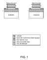
- FIGS. 1-8In order to illustrate the basic principles of this invention, several example structures and their resulting etch profiles are presented in cross-sectional schematic views in FIGS. 1-8 . These examples cover a range of layer configurations including structures with and without “highly resistive/electron-blocking layers”, with various cathode placements.
- the etch selectivityis dependent on the photo-generated carriers, as well as the appropriate conduction path for photo-generated electrons.
- the inefficient removal of electronsslows or inhibits etching in layers in which photo-generated electron-hole pairs recombine faster than they are able to interact with the electrolyte.
- the highly selective etch described in this inventionis precisely controlled by the use of PEC etching in conjunction with local control of the electrochemical component of the etch process (through the use of “highly resistive/electron-blocking layers” and selective cathode placement), and cannot be achieved with bandgap selective PEC etching alone.
- the examples in the preferred embodimentare limited to bandgap-selective lateral etching. However, the invention may also be applied to dopant-selective and/or defect-selective vertical and/or lateral PEC etching.
- FIG. 9A schematic of the PEC etch set-up and two band diagrams illustrating the general principles of PEC etching (doping-selective and bandgap-selective) are shown in FIG. 9 .
- FIGS. 10( a )-( e )cross-sectional schematics are shown for each fabrication step used to make a microdisk.
- the material structureis shown in FIG. 10( a ). Each layer is labeled with material composition and doping, as well as layer type.
- the material structureis grown by metalorganic chemical vapor deposition (MOCVD) on a sapphire substrate.
- MOCVDmetalorganic chemical vapor deposition
- a chlorine-based reactive ion etching (RIE) stepis used to transfer the photoresist pattern to the underlying material.
- the etch depthis approximately 440 nm, such that the entire thickness of the post region is exposed.
- the dry etch maskis removed. The dry-etched structure following mask removal is shown in FIG. 10( c ).
- the etched pillarsare masked with 20 micron diameter concentric circles of photoresist, while the region on which the Pt is to be deposited is left bare.
- the pillaris undercut using PEC etching.
- the structureis placed in a 0.004 M HCl electrolytic solution, under a 1000 W Xe lamp.
- the light from the lampis filtered with an unintentionally doped GaN filter, such that the output power density at 380 nm is 3.5 mW/cm2.
- the electrolyte solutionis stirred during etching.
- a lateral etch rate of 25-35 nm/minis achieved under these conditions.
- the complete undercut deviceis shown in FIG. 10( e ).
- FIG. 11A scanning electron micrograph of the final microdisk structure is shown in FIG. 11 . Note that due to the presence of the Al 0.2 Ga 0.8 N layer (or “highly resistive/electron-blocking” layer) we are able to selectively remove the post layer (or “PEC etched” layer), while leaving the lower-bandgap quantum well layers (or “etch-susceptible” layers) unetched.
- Photoluminescence spectra of unprocessed material and a 3.5 micron diameter microdiskare shown in FIG. 12 .
- the microdisk cavity created using the etching techniqueclearly still contains the quantum well active region.
- the FWHM (full-width half-maximum) of the emission peakis 0.1 nm and central wavelength is 414 nm, therefore a quality factor of about 4600 is achieved. This quality factor is much higher than previously reported measurements of nitride-based microdisks.
- DBRDistributed Bragg Reflector
- FIGS. 13( a )-( e )cross-sectional schematics are shown for each fabrication step used to make a vertically oriented DBR.
- the material structureis shown in FIG. 13( a ). Each layer is labeled with material composition and doping, as well as layer type. The material structure is grown by MOCVD on a sapphire substrate.
- a chlorine-based RIE stepis used to transfer the photoresist pattern to the underlying material.
- the etch depthis approximately 660 nm, such that the entire thickness of the post region is exposed.
- the dry etch maskis removed. The dry-etched structure following mask removal is shown in FIG. 13( c ).
- the pillarsare masked with a striped photoresist pattern such that the openings in the photoresist are aligned to the centers of the pillars.
- the cathode layersare deposited using angled, rotating electron beam evaporation.
- the cathodeis a bilayer of metal consisting of 10 nm Ti and 300 nm Au.
- a lift-off stepis performed leaving cathode material contacting the entire edge and sidewall of each pillar.
- the structure, following cathode deposition and lift-off,is shown in FIG. 13( d ).
- the structureis placed in a 0.004 M HCl electrolytic solution under a 1000 W Xe lamp.
- the light from the lampis filtered with a wafer of unintentionally doped GaN such that the output power density at 380 nm is 3.5 mW/cm2.
- the electrolyte solutionis stirred during etching.
- a lateral etch rate of 25-35 nm/minis achieved under these conditions.
- the complete undercut structureis shown in FIG. 13( e ).
- FIG. 14A scanning electron microscope (SEM) image of the final DBR structure is shown in FIG. 14 . Because the cathode was in direct contact with each of the “PEC etched” layers or the “etch-resistant” layers, each of these layers was etched to almost the same extent.
- Alternate substrate materialsincluding but not limited to r-plane sapphire (Al 2 O 3 ), c-plane silicon carbide (SiC), a-plane SiC, free-standing c-plane GaN, free-standing a-plane GaN, and epitaxial lateral overgrowth (ELOG) GaN on sapphire and SiC may be used.
- r-plane sapphireAl 2 O 3
- SiCc-plane silicon carbide
- SiCsilicon carbide
- ELOGepitaxial lateral overgrowth
- MBEmolecular beam epitaxy
- HVPEhydride vapor phase epitaxy
- a variety of different growth conditionsprecursor sources, gases, temperatures and pressures
- a wide range of compositions, dopant types and dopant concentrationsmay be used to produce the desired type of layer in the semiconductor structure.
- Alternate techniquesincluding but not limited to ion implantation, thermal diffusion, and ion damage may be employed to create the desired type of layer (etch-susceptible, etched, etch resistant or highly resistive/electron-blocking) in the semiconductor structure.
- Alternate etching techniquesincluding but not limited to ICP etching, PEC etching, and focused ion beam etching may be used to perform the vertical etch.
- Alternate metals and combinations thereofalloys or layered structures, metallic oxides, and degenerately doped layers may be employed to serve as the cathode during the bandgap-selective lateral PEC etching.
- Alternate light sourcesincluding but not limited to various broad spectrum sources (with or without filters) and lasers may be employed to carry out the bandgap-selective lateral PEC etching.
- This inventionpermits the uniform etching of specific layers (“PEC etched” layers) in a semiconductor structure through controlled collection of photo-generated carriers, while other specific layers (“etch susceptible” layers) in the same structure are left unetched even though they may contain photo-generated carriers during PEC etching.
- This inventionhas allowed for the fabrication of very high-quality “mushroom-shaped” microdisk resonators with quality factors orders of magnitude higher than previously reported in the nitride material system.
- This inventionhas allowed for the fabrication of high-quality vertically oriented air-gap DBR structures, which have not been previously reported in the nitride material system.
- This inventioncan also be used in several other applications including the fabrication of electrical and optical apertures, semiconductor membranes, cantilevers and photonic crystals, and for substrate removal in the nitride material system.
- Appendix BAbstract, proceedings paper and presentation slides by E. D. Haberer, C. Meier, R. Sharma, A. R. Stonas, S. P. DenBaars, S. Nakamura, and E. L. Hu, “Observation of high Q resonant modes in optically pumped GaN/InGaN microdisks fabricated using photoelectrochemical etching,” International on Workshop Nitride Semiconductors (IWNS), July 2004, Pittsburgh, Pa.
- IWNSInternational on Workshop Nitride Semiconductors
- Appendix CManuscript by E. D. Haberer, R. Sharma, C. Meier, A. R. Stonas, S. Nakamura, S. P. DenBaars, and E. L. Hu, “Free-standing, optically-pumped, GaN/InGaN microdisk lasers fabricated by photoelectrochemical etching,” submitted for publication in Applied Physics Letters in June 2004.
Landscapes
- Engineering & Computer Science (AREA)
- Physics & Mathematics (AREA)
- Chemical & Material Sciences (AREA)
- Condensed Matter Physics & Semiconductors (AREA)
- Optics & Photonics (AREA)
- General Physics & Mathematics (AREA)
- Nanotechnology (AREA)
- Biophysics (AREA)
- Microelectronics & Electronic Packaging (AREA)
- Power Engineering (AREA)
- Life Sciences & Earth Sciences (AREA)
- Electromagnetism (AREA)
- Computer Hardware Design (AREA)
- Crystallography & Structural Chemistry (AREA)
- Manufacturing & Machinery (AREA)
- Weting (AREA)
- Micromachines (AREA)
- Semiconductor Lasers (AREA)
- Led Devices (AREA)
Abstract
Description
Claims (8)
Priority Applications (5)
| Application Number | Priority Date | Filing Date | Title |
|---|---|---|---|
| US11/263,314US7550395B2 (en) | 2004-11-02 | 2005-10-31 | Control of photoelectrochemical (PEC) etching by modification of the local electrochemical potential of the semiconductor structure relative to the electrolyte |
| JP2007539343AJP4825218B2 (en) | 2004-11-02 | 2005-11-02 | Control of photoelectrochemical (PEC) etching by modifying the local electrochemical potential of the semiconductor structure relative to the electrolyte |
| EP05851344AEP1815504A1 (en) | 2004-11-02 | 2005-11-02 | Control of photoelectrochemical (pec) etching by modification of the local electrochemical potential of the semiconductor structure relative to the electrolyte |
| PCT/US2005/039862WO2006050469A1 (en) | 2004-11-02 | 2005-11-02 | Control of photoelectrochemical (pec) etching by modification of the local electrochemical potential of the semiconductor structure relative to the electrolyte |
| JP2010105978AJP2010212718A (en) | 2004-11-02 | 2010-04-30 | Control of photoelectrochemical (pec) etching by modification of local electrochemical potential of semiconductor structure relative to electrolyte |
Applications Claiming Priority (2)
| Application Number | Priority Date | Filing Date | Title |
|---|---|---|---|
| US62430804P | 2004-11-02 | 2004-11-02 | |
| US11/263,314US7550395B2 (en) | 2004-11-02 | 2005-10-31 | Control of photoelectrochemical (PEC) etching by modification of the local electrochemical potential of the semiconductor structure relative to the electrolyte |
Publications (2)
| Publication Number | Publication Date |
|---|---|
| US20060110926A1 US20060110926A1 (en) | 2006-05-25 |
| US7550395B2true US7550395B2 (en) | 2009-06-23 |
Family
ID=36026871
Family Applications (1)
| Application Number | Title | Priority Date | Filing Date |
|---|---|---|---|
| US11/263,314Active - Reinstated2027-01-11US7550395B2 (en) | 2004-11-02 | 2005-10-31 | Control of photoelectrochemical (PEC) etching by modification of the local electrochemical potential of the semiconductor structure relative to the electrolyte |
Country Status (4)
| Country | Link |
|---|---|
| US (1) | US7550395B2 (en) |
| EP (1) | EP1815504A1 (en) |
| JP (2) | JP4825218B2 (en) |
| WO (1) | WO2006050469A1 (en) |
Cited By (5)
| Publication number | Priority date | Publication date | Assignee | Title |
|---|---|---|---|---|
| US20080182420A1 (en)* | 2006-11-15 | 2008-07-31 | The Regents Of The University Of California | Ion beam treatment for the structural integrity of air-gap iii-nitride devices produced by the photoelectrochemical (pec) etching |
| US20100090240A1 (en)* | 2008-10-09 | 2010-04-15 | The Regents Of The University Of California | Photoelectrochemical etching for chip shaping of light emitting diodes |
| US20130248911A1 (en)* | 2012-03-22 | 2013-09-26 | Samsung Electronics Co., Ltd. | Light-emitting device including nitride-based semiconductor omnidirectional reflector |
| WO2014015337A3 (en)* | 2012-07-20 | 2015-07-16 | The Regents Of The University Of California | Gallium nitride vertical cavity laser fabrication method |
| US9773704B2 (en) | 2012-02-17 | 2017-09-26 | The Regents Of The University Of California | Method for the reuse of gallium nitride epitaxial substrates |
Families Citing this family (46)
| Publication number | Priority date | Publication date | Assignee | Title |
|---|---|---|---|---|
| CN100481544C (en)* | 2006-08-11 | 2009-04-22 | 晶元光电股份有限公司 | Method for manufacturing light emitting diode using electroless plating method |
| TWI319893B (en)* | 2006-08-31 | 2010-01-21 | Nitride semiconductor substrate, method for forming a nitride semiconductor layer and method for separating the nitride semiconductor layer from the substrate | |
| EP2286148A1 (en)* | 2008-05-12 | 2011-02-23 | The Regents of the University of California | Photoelectrochemical roughening of p-side-up gan-based light emitting diodes |
| JP2009283807A (en)* | 2008-05-26 | 2009-12-03 | Canon Inc | Structure including nitride semiconductor layer, composite substrate including nitride semiconductor layer, and method for manufacturing them |
| JP5161759B2 (en)* | 2008-12-26 | 2013-03-13 | 富士通株式会社 | Method for manufacturing compound semiconductor device |
| US8263500B2 (en)* | 2009-01-30 | 2012-09-11 | The Regents Of The University Of California | Photoelectrochemical etching for laser facets |
| JP5961557B2 (en) | 2010-01-27 | 2016-08-02 | イェイル ユニヴァーシティ | Conductivity-based selective etching for GaN devices and applications thereof |
| JP2011164299A (en)* | 2010-02-08 | 2011-08-25 | Univ Of Tokyo | Method of manufacturing optical waveguide resonator and method of manufacturing resonator circuit |
| US9293887B2 (en)* | 2011-06-17 | 2016-03-22 | California Institute Of Technology | Chip-based laser resonator device for highly coherent laser generation |
| TWI447950B (en)* | 2011-07-14 | 2014-08-01 | Lextar Electronics Corp | Leds and methods for manufacturing the same |
| TWI460885B (en)* | 2011-12-09 | 2014-11-11 | Univ Nat Chiao Tung | Semiconductor optoelectronic component with air dielectric layer and method for manufacturing air dielectric layer |
| US9583353B2 (en)* | 2012-06-28 | 2017-02-28 | Yale University | Lateral electrochemical etching of III-nitride materials for microfabrication |
| CN105283946A (en)* | 2013-03-14 | 2016-01-27 | 阿卜杜拉国王科技大学 | Defect-free monocrystalline thin layer |
| US9362715B2 (en) | 2014-02-10 | 2016-06-07 | Soraa Laser Diode, Inc | Method for manufacturing gallium and nitrogen bearing laser devices with improved usage of substrate material |
| US9379525B2 (en) | 2014-02-10 | 2016-06-28 | Soraa Laser Diode, Inc. | Manufacturable laser diode |
| US9368939B2 (en) | 2013-10-18 | 2016-06-14 | Soraa Laser Diode, Inc. | Manufacturable laser diode formed on C-plane gallium and nitrogen material |
| US9520695B2 (en) | 2013-10-18 | 2016-12-13 | Soraa Laser Diode, Inc. | Gallium and nitrogen containing laser device having confinement region |
| EP3097615B1 (en) | 2014-01-24 | 2020-03-11 | California Institute Of Technology | Stabilized microwave-frequency source |
| US9209596B1 (en)* | 2014-02-07 | 2015-12-08 | Soraa Laser Diode, Inc. | Manufacturing a laser diode device from a plurality of gallium and nitrogen containing substrates |
| US9871350B2 (en) | 2014-02-10 | 2018-01-16 | Soraa Laser Diode, Inc. | Manufacturable RGB laser diode source |
| US9520697B2 (en) | 2014-02-10 | 2016-12-13 | Soraa Laser Diode, Inc. | Manufacturable multi-emitter laser diode |
| US11095096B2 (en) | 2014-04-16 | 2021-08-17 | Yale University | Method for a GaN vertical microcavity surface emitting laser (VCSEL) |
| CN107078190B (en) | 2014-09-30 | 2020-09-08 | 耶鲁大学 | Methods for GaN Vertical Microcavity Surface Emitting Lasers (VCSELs) |
| US12126143B2 (en) | 2014-11-06 | 2024-10-22 | Kyocera Sld Laser, Inc. | Method of manufacture for an ultraviolet emitting optoelectronic device |
| US9246311B1 (en) | 2014-11-06 | 2016-01-26 | Soraa Laser Diode, Inc. | Method of manufacture for an ultraviolet laser diode |
| US11018231B2 (en) | 2014-12-01 | 2021-05-25 | Yale University | Method to make buried, highly conductive p-type III-nitride layers |
| US9653642B1 (en) | 2014-12-23 | 2017-05-16 | Soraa Laser Diode, Inc. | Manufacturable RGB display based on thin film gallium and nitrogen containing light emitting diodes |
| US9666677B1 (en) | 2014-12-23 | 2017-05-30 | Soraa Laser Diode, Inc. | Manufacturable thin film gallium and nitrogen containing devices |
| WO2016138291A1 (en) | 2015-02-26 | 2016-09-01 | California Institute Of Technology | Optical frequency divider based on an electro-optical-modulator frequency comb |
| US10554017B2 (en) | 2015-05-19 | 2020-02-04 | Yale University | Method and device concerning III-nitride edge emitting laser diode of high confinement factor with lattice matched cladding layer |
| US11437774B2 (en) | 2015-08-19 | 2022-09-06 | Kyocera Sld Laser, Inc. | High-luminous flux laser-based white light source |
| US10879673B2 (en) | 2015-08-19 | 2020-12-29 | Soraa Laser Diode, Inc. | Integrated white light source using a laser diode and a phosphor in a surface mount device package |
| US11437775B2 (en) | 2015-08-19 | 2022-09-06 | Kyocera Sld Laser, Inc. | Integrated light source using a laser diode |
| US10938182B2 (en) | 2015-08-19 | 2021-03-02 | Soraa Laser Diode, Inc. | Specialized integrated light source using a laser diode |
| BE1025681B1 (en) | 2018-03-23 | 2019-05-28 | Universite Catholique De Louvain | Method of processing a substrate and integrated circuit device |
| US11421843B2 (en) | 2018-12-21 | 2022-08-23 | Kyocera Sld Laser, Inc. | Fiber-delivered laser-induced dynamic light system |
| US11239637B2 (en) | 2018-12-21 | 2022-02-01 | Kyocera Sld Laser, Inc. | Fiber delivered laser induced white light system |
| US12152742B2 (en) | 2019-01-18 | 2024-11-26 | Kyocera Sld Laser, Inc. | Laser-based light guide-coupled wide-spectrum light system |
| US12000552B2 (en) | 2019-01-18 | 2024-06-04 | Kyocera Sld Laser, Inc. | Laser-based fiber-coupled white light system for a vehicle |
| US11884202B2 (en) | 2019-01-18 | 2024-01-30 | Kyocera Sld Laser, Inc. | Laser-based fiber-coupled white light system |
| JP7254639B2 (en)* | 2019-04-26 | 2023-04-10 | 住友化学株式会社 | Element manufacturing method |
| US11393693B2 (en) | 2019-04-26 | 2022-07-19 | Sciocs Company Limited | Structure manufacturing method and intermediate structure |
| US11228158B2 (en) | 2019-05-14 | 2022-01-18 | Kyocera Sld Laser, Inc. | Manufacturable laser diodes on a large area gallium and nitrogen containing substrate |
| US10903623B2 (en) | 2019-05-14 | 2021-01-26 | Soraa Laser Diode, Inc. | Method and structure for manufacturable large area gallium and nitrogen containing substrate |
| US12191626B1 (en) | 2020-07-31 | 2025-01-07 | Kyocera Sld Laser, Inc. | Vertically emitting laser devices and chip-scale-package laser devices and laser-based, white light emitting devices |
| JP7081000B2 (en)* | 2021-01-04 | 2022-06-06 | スタンレー電気株式会社 | Vertical resonator type light emitting element |
Citations (7)
| Publication number | Priority date | Publication date | Assignee | Title |
|---|---|---|---|---|
| US5773369A (en)* | 1996-04-30 | 1998-06-30 | The Regents Of The University Of California | Photoelectrochemical wet etching of group III nitrides |
| US5895223A (en) | 1997-12-10 | 1999-04-20 | Industrial Technology Research Institute | Method for etching nitride |
| US6306672B1 (en) | 1997-07-24 | 2001-10-23 | Samsung Electronics Co., Ltd. | Group III-V complex vertical cavity surface emitting laser diode and method for manufacturing the same |
| US20030045120A1 (en) | 2001-09-04 | 2003-03-06 | Hu Evelyn L. | Photoelectrochemical undercut etching of semiconductor material |
| US6605548B1 (en) | 1999-06-01 | 2003-08-12 | National Research Council Of Canada | Process for etching gallium nitride compound based semiconductors |
| US20030180980A1 (en) | 2001-12-21 | 2003-09-25 | Tal Margalith | Implantation for current confinement in nitride-based vertical optoelectronics |
| US7026255B2 (en)* | 2002-12-04 | 2006-04-11 | Thomas Wolff | Method and device for photo-electrochemically etching a semiconductor sample, especially gallium nitride |
Family Cites Families (3)
| Publication number | Priority date | Publication date | Assignee | Title |
|---|---|---|---|---|
| JPH08203862A (en)* | 1995-01-27 | 1996-08-09 | Matsushita Electric Ind Co Ltd | Etching method for nitride compound semiconductor |
| JP2002270572A (en)* | 2001-03-07 | 2002-09-20 | Mitsubishi Electric Corp | Semiconductor device manufacturing method and manufacturing apparatus used for the same |
| JP2003218087A (en)* | 2002-01-22 | 2003-07-31 | Mitsubishi Electric Corp | Method for manufacturing semiconductor device |
- 2005
- 2005-10-31USUS11/263,314patent/US7550395B2/enactiveActive - Reinstated
- 2005-11-02WOPCT/US2005/039862patent/WO2006050469A1/enactiveApplication Filing
- 2005-11-02JPJP2007539343Apatent/JP4825218B2/ennot_activeExpired - Fee Related
- 2005-11-02EPEP05851344Apatent/EP1815504A1/ennot_activeWithdrawn
- 2010
- 2010-04-30JPJP2010105978Apatent/JP2010212718A/enactivePending
Patent Citations (7)
| Publication number | Priority date | Publication date | Assignee | Title |
|---|---|---|---|---|
| US5773369A (en)* | 1996-04-30 | 1998-06-30 | The Regents Of The University Of California | Photoelectrochemical wet etching of group III nitrides |
| US6306672B1 (en) | 1997-07-24 | 2001-10-23 | Samsung Electronics Co., Ltd. | Group III-V complex vertical cavity surface emitting laser diode and method for manufacturing the same |
| US5895223A (en) | 1997-12-10 | 1999-04-20 | Industrial Technology Research Institute | Method for etching nitride |
| US6605548B1 (en) | 1999-06-01 | 2003-08-12 | National Research Council Of Canada | Process for etching gallium nitride compound based semiconductors |
| US20030045120A1 (en) | 2001-09-04 | 2003-03-06 | Hu Evelyn L. | Photoelectrochemical undercut etching of semiconductor material |
| US20030180980A1 (en) | 2001-12-21 | 2003-09-25 | Tal Margalith | Implantation for current confinement in nitride-based vertical optoelectronics |
| US7026255B2 (en)* | 2002-12-04 | 2006-04-11 | Thomas Wolff | Method and device for photo-electrochemically etching a semiconductor sample, especially gallium nitride |
Non-Patent Citations (15)
| Title |
|---|
| Ben-Yaacov et al., "AlGaN/GaN current aperture vertical electron transistors," Device Research Conference (Cat. No. 02TH8606), IEEE, 2002, pp. 31-32. |
| Edwards et al, "InGaN/GaN quantum well microcavities formed by laser lift-off and plasma etching," Wiley-VCH. Physica Status Solidi B-Basic Research, vol. 228, No. 1, pp. 91-94, 2001. |
| Gao Y. et al: "Al GaN/GaN current aperture vertical electron transistors fabricated by photoelectrochemical wet etching" Electronics Letters, IEE Stevenage, GB, vol. 39, No. 1, Jan. 9, 2003, pp. 148-149. |
| Haberer E. D. et al: "Removal of thick (> 100 nm) InGaN layers for optical devices using band-gap-selective photoelectrochemical etching" Applied Physics Letters, vol. 85, No. 5, Aug. 2, 2004, pp. 762-764. |
| Martin et al., "GaN microcavities formed by laser lift-off and plasma etching," Materials Science & Engineering B-Solid State Materials for Advanced Technology, vol. B93, pp. 98-101, 2002. |
| Martin et al., "Optical spectroscopy of GaN microcavities with thicknesses controlled using a plasma etchback," Applied Physics Letters, vol. 79, No. 19, pp. 3029-3031, Nov. 5, 2001. |
| Pearton, S. J.: A review of dry etching of GaN and related materials MRS Internet Journal of Nitride Semiconductor Research, vol. 5, No. 11, Nov. 16, 2000. (Retrieved from the Internet: URL:http:/ /nsr.mij.mrs.org./5/11/complete.html.). |
| Stonas A. R. et al: "Photoelectrochemical undercut etching for fabrication of GaN microelectromechanical systems" Journal of Vacuum Science and Technology. B, Micoelectronics and Nanometer Structures Processing, Measurement and Phenomena, vol. 19, No. 6, Nov. 2001, pp. 2838-2841. |
| Stonas et al., "Backside-illuminated photoelectrochemical etching for the fabrication of deeply undercut GaN structures," Applied Physics Letters, vol. 77, No. 16, pp. 2610-2612, Oct. 16, 2000. |
| Stonas et al., "Development of selective lateral photoelectrochemical etching of InGaN/GaN for lift-off applications," Applied Physics Letters, vol. 78, No. 13, pp. 1945-1947, Mar. 26, 2001. |
| Stonas et al., "Gallium Nitride-Based Micro-Opto-Electro-Mechanical Systems," in Electrical and Computer Engineering Department Santa Barbara: University of California, Santa Barbara, Dec. 2003, pp. 1-132. |
| Strittmatter et al., "Fabrication of GaN suspended microstructures," Applied Physics Letters, vol. 78, No. 21, pp. 3226-3228, May 21, 2001. |
| Wong et al., "Damage-free separation of GaN thin films from sapphire substrates," Applied Physics Letters, vol. 72, No. 5, pp. 599-601, Feb. 2, 1998. |
| Wong et al., "Structural and optical quality of GaN/metal/Si heterostructures fabricated by excimer laser lift-off," Applied Physics Lettes, vol. 75, No. 13, pp. 1887-1889, Sep. 27, 1999. |
| Youtsey et al., "Dopant-selective photoenhanced wet etching of GaN," Journal of Electronic Materials, vol. 27, No. 4, pp. 282-287, Nov. 4, 1998. |
Cited By (9)
| Publication number | Priority date | Publication date | Assignee | Title |
|---|---|---|---|---|
| US20080182420A1 (en)* | 2006-11-15 | 2008-07-31 | The Regents Of The University Of California | Ion beam treatment for the structural integrity of air-gap iii-nitride devices produced by the photoelectrochemical (pec) etching |
| US20100090240A1 (en)* | 2008-10-09 | 2010-04-15 | The Regents Of The University Of California | Photoelectrochemical etching for chip shaping of light emitting diodes |
| US8569085B2 (en) | 2008-10-09 | 2013-10-29 | The Regents Of The University Of California | Photoelectrochemical etching for chip shaping of light emitting diodes |
| US9773704B2 (en) | 2012-02-17 | 2017-09-26 | The Regents Of The University Of California | Method for the reuse of gallium nitride epitaxial substrates |
| US20130248911A1 (en)* | 2012-03-22 | 2013-09-26 | Samsung Electronics Co., Ltd. | Light-emitting device including nitride-based semiconductor omnidirectional reflector |
| US8941140B2 (en)* | 2012-03-22 | 2015-01-27 | Samsung Electronics Co., Ltd. | Light-emitting device including nitride-based semiconductor omnidirectional reflector |
| WO2014015337A3 (en)* | 2012-07-20 | 2015-07-16 | The Regents Of The University Of California | Gallium nitride vertical cavity laser fabrication method |
| US9136673B2 (en) | 2012-07-20 | 2015-09-15 | The Regents Of The University Of California | Structure and method for the fabrication of a gallium nitride vertical cavity surface emitting laser |
| US9640947B2 (en) | 2012-07-20 | 2017-05-02 | The Regents Of The University Of California | Structure and method for the fabrication of a gallium nitride vertical cavity surface emitting laser |
Also Published As
| Publication number | Publication date |
|---|---|
| US20060110926A1 (en) | 2006-05-25 |
| WO2006050469A1 (en) | 2006-05-11 |
| JP4825218B2 (en) | 2011-11-30 |
| JP2010212718A (en) | 2010-09-24 |
| EP1815504A1 (en) | 2007-08-08 |
| JP2008519442A (en) | 2008-06-05 |
Similar Documents
| Publication | Publication Date | Title |
|---|---|---|
| US7550395B2 (en) | Control of photoelectrochemical (PEC) etching by modification of the local electrochemical potential of the semiconductor structure relative to the electrolyte | |
| KR102467783B1 (en) | Methods and semiconductor structures for porous materials | |
| US8975615B2 (en) | Method of fabricating optical devices using laser treatment of contact regions of gallium and nitrogen containing material | |
| US9786810B2 (en) | Method of fabricating optical devices using laser treatment | |
| US11348908B2 (en) | Contact architectures for tunnel junction devices | |
| US9396943B2 (en) | Method for the reuse of gallium nitride epitaxial substrates | |
| TWI520206B (en) | Method for at least partially separating an epitaxial layer | |
| US9583353B2 (en) | Lateral electrochemical etching of III-nitride materials for microfabrication | |
| US20100316075A1 (en) | Optical Device Structure Using GaN Substrates for Laser Applications | |
| KR20170063919A (en) | A METHOD FOR GaN VERTICAL MICROCAVITY SURFACE EMITTING LASER (VCSEL) | |
| US9142935B2 (en) | Laser diodes with scribe structures | |
| KR20110110846A (en) | Photoelectrochemical Etching for Laser Facets | |
| Holder et al. | Demonstration of nonpolar GaN-based vertical-cavity surface-emitting lasers | |
| WO2025035077A1 (en) | Chemical etch assembly for uniform iii-nitride based etching | |
| Hjort | Ultraviolet vertical-cavity surface-emitting lasers and vertical microcavities for blue lasers |
Legal Events
| Date | Code | Title | Description |
|---|---|---|---|
| AS | Assignment | Owner name:REGENTS OF THE UNIVERSITY OF CALIFORNIA, THE, CALI Free format text:ASSIGNMENT OF ASSIGNORS INTEREST;ASSIGNORS:HU, EVELYN L.;NAKAMURA, SHUJI;HABERER, ELAINE D.;AND OTHERS;REEL/FRAME:017185/0749;SIGNING DATES FROM 20051021 TO 20051024 | |
| FEPP | Fee payment procedure | Free format text:PAT HOLDER CLAIMS SMALL ENTITY STATUS, ENTITY STATUS SET TO SMALL (ORIGINAL EVENT CODE: LTOS); ENTITY STATUS OF PATENT OWNER: SMALL ENTITY | |
| FPAY | Fee payment | Year of fee payment:4 | |
| REMI | Maintenance fee reminder mailed | ||
| LAPS | Lapse for failure to pay maintenance fees | ||
| STCH | Information on status: patent discontinuation | Free format text:PATENT EXPIRED DUE TO NONPAYMENT OF MAINTENANCE FEES UNDER 37 CFR 1.362 | |
| FP | Lapsed due to failure to pay maintenance fee | Effective date:20170623 | |
| FEPP | Fee payment procedure | Free format text:ENTITY STATUS SET TO UNDISCOUNTED (ORIGINAL EVENT CODE: BIG.); ENTITY STATUS OF PATENT OWNER: LARGE ENTITY | |
| FEPP | Fee payment procedure | Free format text:PETITION RELATED TO MAINTENANCE FEES FILED (ORIGINAL EVENT CODE: PMFP); ENTITY STATUS OF PATENT OWNER: LARGE ENTITY Free format text:SURCHARGE, PETITION TO ACCEPT PYMT AFTER EXP, UNINTENTIONAL (ORIGINAL EVENT CODE: M1558); ENTITY STATUS OF PATENT OWNER: LARGE ENTITY | |
| MAFP | Maintenance fee payment | Free format text:PAYMENT OF MAINTENANCE FEE, 8TH YEAR, LARGE ENTITY (ORIGINAL EVENT CODE: M1552); ENTITY STATUS OF PATENT OWNER: LARGE ENTITY Year of fee payment:8 | |
| PRDP | Patent reinstated due to the acceptance of a late maintenance fee | Effective date:20200220 | |
| FEPP | Fee payment procedure | Free format text:PETITION RELATED TO MAINTENANCE FEES GRANTED (ORIGINAL EVENT CODE: PMFG); ENTITY STATUS OF PATENT OWNER: LARGE ENTITY | |
| STCF | Information on status: patent grant | Free format text:PATENTED CASE | |
| FEPP | Fee payment procedure | Free format text:ENTITY STATUS SET TO SMALL (ORIGINAL EVENT CODE: SMAL); ENTITY STATUS OF PATENT OWNER: SMALL ENTITY | |
| MAFP | Maintenance fee payment | Free format text:PAYMENT OF MAINTENANCE FEE, 12TH YR, SMALL ENTITY (ORIGINAL EVENT CODE: M2553); ENTITY STATUS OF PATENT OWNER: SMALL ENTITY Year of fee payment:12 |