US7550370B2 - Method of forming thin SGOI wafers with high relaxation and low stacking fault defect density - Google Patents
Method of forming thin SGOI wafers with high relaxation and low stacking fault defect densityDownload PDFInfo
- Publication number
- US7550370B2 US7550370B2US10/597,066US59706604AUS7550370B2US 7550370 B2US7550370 B2US 7550370B2US 59706604 AUS59706604 AUS 59706604AUS 7550370 B2US7550370 B2US 7550370B2
- Authority
- US
- United States
- Prior art keywords
- layer
- sige
- sgoi
- sige layer
- stacking fault
- Prior art date
- Legal status (The legal status is an assumption and is not a legal conclusion. Google has not performed a legal analysis and makes no representation as to the accuracy of the status listed.)
- Expired - Fee Related, expires
Links
Images


Classifications
- H—ELECTRICITY
- H01—ELECTRIC ELEMENTS
- H01L—SEMICONDUCTOR DEVICES NOT COVERED BY CLASS H10
- H01L21/00—Processes or apparatus adapted for the manufacture or treatment of semiconductor or solid state devices or of parts thereof
- H01L21/02—Manufacture or treatment of semiconductor devices or of parts thereof
- H01L21/04—Manufacture or treatment of semiconductor devices or of parts thereof the devices having potential barriers, e.g. a PN junction, depletion layer or carrier concentration layer
- H01L21/18—Manufacture or treatment of semiconductor devices or of parts thereof the devices having potential barriers, e.g. a PN junction, depletion layer or carrier concentration layer the devices having semiconductor bodies comprising elements of Group IV of the Periodic Table or AIIIBV compounds with or without impurities, e.g. doping materials
- H01L21/20—Deposition of semiconductor materials on a substrate, e.g. epitaxial growth solid phase epitaxy
- H—ELECTRICITY
- H01—ELECTRIC ELEMENTS
- H01L—SEMICONDUCTOR DEVICES NOT COVERED BY CLASS H10
- H01L21/00—Processes or apparatus adapted for the manufacture or treatment of semiconductor or solid state devices or of parts thereof
- H01L21/02—Manufacture or treatment of semiconductor devices or of parts thereof
- H01L21/02104—Forming layers
- H01L21/02107—Forming insulating materials on a substrate
- H01L21/02225—Forming insulating materials on a substrate characterised by the process for the formation of the insulating layer
- H01L21/02227—Forming insulating materials on a substrate characterised by the process for the formation of the insulating layer formation by a process other than a deposition process
- H01L21/0223—Forming insulating materials on a substrate characterised by the process for the formation of the insulating layer formation by a process other than a deposition process formation by oxidation, e.g. oxidation of the substrate
- H01L21/02233—Forming insulating materials on a substrate characterised by the process for the formation of the insulating layer formation by a process other than a deposition process formation by oxidation, e.g. oxidation of the substrate of the semiconductor substrate or a semiconductor layer
- H01L21/02236—Forming insulating materials on a substrate characterised by the process for the formation of the insulating layer formation by a process other than a deposition process formation by oxidation, e.g. oxidation of the substrate of the semiconductor substrate or a semiconductor layer group IV semiconductor
- H—ELECTRICITY
- H01—ELECTRIC ELEMENTS
- H01L—SEMICONDUCTOR DEVICES NOT COVERED BY CLASS H10
- H01L21/00—Processes or apparatus adapted for the manufacture or treatment of semiconductor or solid state devices or of parts thereof
- H01L21/02—Manufacture or treatment of semiconductor devices or of parts thereof
- H01L21/02104—Forming layers
- H01L21/02107—Forming insulating materials on a substrate
- H01L21/02225—Forming insulating materials on a substrate characterised by the process for the formation of the insulating layer
- H01L21/02227—Forming insulating materials on a substrate characterised by the process for the formation of the insulating layer formation by a process other than a deposition process
- H01L21/02255—Forming insulating materials on a substrate characterised by the process for the formation of the insulating layer formation by a process other than a deposition process formation by thermal treatment
- H—ELECTRICITY
- H01—ELECTRIC ELEMENTS
- H01L—SEMICONDUCTOR DEVICES NOT COVERED BY CLASS H10
- H01L21/00—Processes or apparatus adapted for the manufacture or treatment of semiconductor or solid state devices or of parts thereof
- H01L21/02—Manufacture or treatment of semiconductor devices or of parts thereof
- H01L21/02104—Forming layers
- H01L21/02365—Forming inorganic semiconducting materials on a substrate
- H01L21/02367—Substrates
- H01L21/0237—Materials
- H01L21/02373—Group 14 semiconducting materials
- H01L21/02381—Silicon, silicon germanium, germanium
- H—ELECTRICITY
- H01—ELECTRIC ELEMENTS
- H01L—SEMICONDUCTOR DEVICES NOT COVERED BY CLASS H10
- H01L21/00—Processes or apparatus adapted for the manufacture or treatment of semiconductor or solid state devices or of parts thereof
- H01L21/02—Manufacture or treatment of semiconductor devices or of parts thereof
- H01L21/02104—Forming layers
- H01L21/02365—Forming inorganic semiconducting materials on a substrate
- H01L21/02436—Intermediate layers between substrates and deposited layers
- H01L21/02439—Materials
- H01L21/02441—Group 14 semiconducting materials
- H01L21/0245—Silicon, silicon germanium, germanium
- H—ELECTRICITY
- H01—ELECTRIC ELEMENTS
- H01L—SEMICONDUCTOR DEVICES NOT COVERED BY CLASS H10
- H01L21/00—Processes or apparatus adapted for the manufacture or treatment of semiconductor or solid state devices or of parts thereof
- H01L21/02—Manufacture or treatment of semiconductor devices or of parts thereof
- H01L21/02104—Forming layers
- H01L21/02365—Forming inorganic semiconducting materials on a substrate
- H01L21/02518—Deposited layers
- H01L21/02521—Materials
- H01L21/02524—Group 14 semiconducting materials
- H01L21/02532—Silicon, silicon germanium, germanium
- H—ELECTRICITY
- H01—ELECTRIC ELEMENTS
- H01L—SEMICONDUCTOR DEVICES NOT COVERED BY CLASS H10
- H01L21/00—Processes or apparatus adapted for the manufacture or treatment of semiconductor or solid state devices or of parts thereof
- H01L21/02—Manufacture or treatment of semiconductor devices or of parts thereof
- H01L21/02104—Forming layers
- H01L21/02365—Forming inorganic semiconducting materials on a substrate
- H01L21/02656—Special treatments
- H01L21/02664—Aftertreatments
- H—ELECTRICITY
- H01—ELECTRIC ELEMENTS
- H01L—SEMICONDUCTOR DEVICES NOT COVERED BY CLASS H10
- H01L21/00—Processes or apparatus adapted for the manufacture or treatment of semiconductor or solid state devices or of parts thereof
- H01L21/70—Manufacture or treatment of devices consisting of a plurality of solid state components formed in or on a common substrate or of parts thereof; Manufacture of integrated circuit devices or of parts thereof
- H01L21/71—Manufacture of specific parts of devices defined in group H01L21/70
- H01L21/76—Making of isolation regions between components
- H01L21/762—Dielectric regions, e.g. EPIC dielectric isolation, LOCOS; Trench refilling techniques, SOI technology, use of channel stoppers
- H01L21/7624—Dielectric regions, e.g. EPIC dielectric isolation, LOCOS; Trench refilling techniques, SOI technology, use of channel stoppers using semiconductor on insulator [SOI] technology
- H01L21/76251—Dielectric regions, e.g. EPIC dielectric isolation, LOCOS; Trench refilling techniques, SOI technology, use of channel stoppers using semiconductor on insulator [SOI] technology using bonding techniques
- H01L21/76256—Dielectric regions, e.g. EPIC dielectric isolation, LOCOS; Trench refilling techniques, SOI technology, use of channel stoppers using semiconductor on insulator [SOI] technology using bonding techniques using silicon etch back techniques, e.g. BESOI, ELTRAN
- H—ELECTRICITY
- H10—SEMICONDUCTOR DEVICES; ELECTRIC SOLID-STATE DEVICES NOT OTHERWISE PROVIDED FOR
- H10D—INORGANIC ELECTRIC SEMICONDUCTOR DEVICES
- H10D86/00—Integrated devices formed in or on insulating or conducting substrates, e.g. formed in silicon-on-insulator [SOI] substrates or on stainless steel or glass substrates
- H—ELECTRICITY
- H10—SEMICONDUCTOR DEVICES; ELECTRIC SOLID-STATE DEVICES NOT OTHERWISE PROVIDED FOR
- H10D—INORGANIC ELECTRIC SEMICONDUCTOR DEVICES
- H10D30/00—Field-effect transistors [FET]
- H10D30/60—Insulated-gate field-effect transistors [IGFET]
- H10D30/67—Thin-film transistors [TFT]
- H10D30/674—Thin-film transistors [TFT] characterised by the active materials
- H10D30/6741—Group IV materials, e.g. germanium or silicon carbide
- H10D30/6748—Group IV materials, e.g. germanium or silicon carbide having a multilayer structure or superlattice structure
- H—ELECTRICITY
- H10—SEMICONDUCTOR DEVICES; ELECTRIC SOLID-STATE DEVICES NOT OTHERWISE PROVIDED FOR
- H10D—INORGANIC ELECTRIC SEMICONDUCTOR DEVICES
- H10D30/00—Field-effect transistors [FET]
- H10D30/60—Insulated-gate field-effect transistors [IGFET]
- H10D30/751—Insulated-gate field-effect transistors [IGFET] having composition variations in the channel regions
- H—ELECTRICITY
- H10—SEMICONDUCTOR DEVICES; ELECTRIC SOLID-STATE DEVICES NOT OTHERWISE PROVIDED FOR
- H10D—INORGANIC ELECTRIC SEMICONDUCTOR DEVICES
- H10D86/00—Integrated devices formed in or on insulating or conducting substrates, e.g. formed in silicon-on-insulator [SOI] substrates or on stainless steel or glass substrates
- H10D86/01—Manufacture or treatment
Definitions
- the present inventiongenerally relates to silicon germanium (Si 1-x Ge x , for simplicity referred to as SiGe) on insulator (SGOI) structures and more particularly to an improved method of forming SGOI structures with a thin and highly relaxed SiGe layer, and with low stacking fault defect density.
- CMOScomplementary metal oxide semiconductor
- Si deposited on relaxed SiGeis tensily strained and used as channel material for both N-type field effect transistors (NFETs) and P-type field effect transistors (PFETs).
- NFETsN-type field effect transistors
- PFETsP-type field effect transistors
- the NFETshave significant mobility enhancement at strain of 0.6%; however, more than 1.2% of strain is required for significant PFET mobility enhancement.
- SOISi on Si on insulator
- BOXburied oxide
- stacking fault defects in the Si and SiGe materialcan cause source to drain shorts and need to be minimized.
- U.S. Patent Application Publication 2002/0185686describes a process for fabricating a SGOI layer by growing a pseudomorphic epitaxial SiGe layer on top of SOI, implanting ions of light elements beneath the layer, and then performing a relaxation annealing process.
- U.S. Patent Application Publication 2002/0168802describes a process for fabricating a combined SiGe/SOI structure, in which the top layer of SOI is converted to SiGe and then annealed.
- thermal mixingpseudomorphic SiGe film is deposited on SOI wafers, and a high temperature oxidation (1200° C.-1300° C.) intermixes SiGe with underlying Si, relaxes the SiGe, and makes the SiGe thinner at the same time.
- Geis rejected from the oxide at high temperatures, so the amount of Ge in SiGe layer is substantially conserved.
- a 600 ⁇ , 17% SiGe on SOIcan be mixed to 400 ⁇ , 25% SGOI, or to 1000 ⁇ , 10% SGOI provided that initial SOI thickness is more than 400 ⁇ .
- SGOI film after thermal mixingis normally not 100% relaxed.
- the 400 ⁇ 25% SGOIis only 60% relaxed, which gives about 0.6% strain for Si deposited on this substrate.
- This high concentration SiGe filmhas many additional material issues and CMOS process integration issues compared with lower concentration materials, and is not desired.
- SiGe with relatively low concentration but high relaxationis required.
- a method of forming an SGOI structurebegins by depositing a SiGe layer on an SOI wafer.
- the inventionperforms a thermal mixing process that intermixes the SiGe layer with the underlying Si layer and partially relaxes strain within the SiGe layer.
- the thermal mixing processis usually carried out in an oxidizing environment and the amount of oxidation can be used to control the SiGe thickness after the thermal mixing.
- the inventionthen thins the SiGe layer to a desired final thickness. This thinning process keeps the Ge concentration, the amount of relaxation, and stacking fault defect density unchanged. This way, the invention is able to obtain a thin SGOI film with high relaxation, and with low stacking fault defect density.
- a surface smoothing processis carried out after thinning.
- the inventiondeposits Si on the thin SGOI wafer.
- the process of thermally mixing the SiGe layercomprises heating the SiGe layer to approximately 1200° C.-1300° C. in an oxidizing environment. During such a high temperature oxidation process, Ge atoms are rejected from the oxide and accumulate in the SiGe layer under the oxide.
- the thinning processnon-selectively thins the SiGe layer such that Si and Ge within the SiGe layer are removed according to their existing molar concentrations. More specifically, the thinning process can be a high pressure oxidation (HIPOX) process conducted at a temperature less than 700° C., a steam oxidation process conducted at a temperature of less than 700° C., an HCl etching process, or an chemical mechanical polishing (CMP) process. If the oxidation thinning process is used, the SiGe layer is substantially smoothed by a smoothing process after thinning and has a surface roughness of less than 15 ⁇ , preferably less than 10 ⁇ .
- HIPOXhigh pressure oxidation
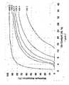
- FIG. 1shows relationship of the remaining strain in SGOI after thermal mixing and the SiGe thickness
- FIG. 2shows the percentage of SGOI relaxation dependence on the Ge concentration and the SiGe thickness
- FIG. 3shows relationship of the stacking fault defect density in SGOI and the SiGe thickness
- FIGS. 4-9are schematic diagrams (through cross sectional views) illustrating the basic processing steps that are employed in the present invention.
- FIG. 10is a flow diagram illustrating a preferred method of the invention.
- FIG. 1shows the relationship of the remaining strain in SGOI after thermal mixing and the SiGe thickness.
- the dash curveshows experimental data, and the solid curve shows theoretical data.
- FIG. 1shows that dislocation formation reduces strain in the SiGe film and that the film relaxes until strain energy is below the level necessary to form new dislocations.
- the theory and experimental datafit well down to SiGe thickness of 500 ⁇ . Below 500 ⁇ , experimental data shows more remaining strain, thus less relaxed than predicted by theory.
- FIG. 2shows the percentage of SGOI relaxation dependence on Ge concentration and SiGe thickness as predicted by theory. As pointed out earlier, experimental data shows less relaxation than predicted by theory when SiGe film thickness is less than 500 ⁇ . These data show that for a given Ge concentration, the percentage of relaxation increases when SiGe film thickness increases. For example, for 20% SiGe, the theory predicts 30% relaxation for 200 ⁇ SiGe film, and 80% relaxation for 1000 ⁇ SiGe film.
- FIG. 3shows the relationship of stacking fault defect density (a planar-type defect associated with an error in atomic order of the crystalline structure) in SGOI and the SiGe thickness found by the inventors.
- stacking fault defect densitya planar-type defect associated with an error in atomic order of the crystalline structure
- SiGe thicknessfound by the inventors.
- the stacking fault defect densityis reduced by one order of magnitude.
- the SGOIhas less than 1 ⁇ 10 4 /cm 2 (preferably less than 1 ⁇ 10 2 /cm 2 ) of stacking fault defects.
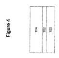
- the inventionfirst deposits a SiGe layer 104 on an SOI 102 and 100 , where 102 is Si layer and 100 is buried oxide (BOX).
- SiGe layer 104can be with uniform Ge concentration, or have Ge concentration variation along the film thickness, such as including a Si buffer layer or cap layer.
- the inventionperforms thermal mixing of the SiGe and Si layers in an oxidizing environment at temperature range of 1200° C.-1300° C., which intermixes the SiGe and Si, at the same time oxidizes and thins the intermixed SiGe layer, and at the same time partially relaxes strain within the SiGe layer.
- a partially relaxed SiGe layer 106is formed directly on top of BOX 100 , and an oxide layer 108 is formed on top of the SiGe layer.
- Some internal oxidationmay occur during thermal mixing; as a result, the thickness of BOX 100 may increase after thermal mixing.
- Geis rejected from the oxide, so the amount of Ge in the SiGe layer 106 is substantially same as the SiGe layer 104 in FIG. 4 .
- the inventionthen removes the oxide layer 108 by a hydrofluoric acid etch.
- An example of an etchant for this processis a 10:1 HF:H 2 O solution.
- the inventionnon-selectively thins the SiGe layer 106 to a desired final thickness; the thinned SiGe layer is illustrated as layer 110 in FIG. 7 .
- This non-selective thinningkeeps the germanium concentration, the amount of relaxation, and stacking fault defect density unchanged. In other words, the thinning process non-selectively thins the SiGe layer such that the Si and Ge within the relaxed SiGe layer are removed proportionately.
- the inventionis able to obtain a thin SGOI film with high relaxation and low stacking fault defect density. While this disclosure discusses four different processes to non-selectively thin the SiGe layer, one ordinarily skilled in the art would understand that additional methods could be used.
- a HIPOX process at a temperature range of 550° C.-700° C.is used to non-selectively oxidize SiGe layer 106 .
- the process pressureis typically at 1-50 ATM, preferably at 5-20 ATM. Steam is typically introduced to increase the oxidation rate. After oxidation, the oxide is removed by an HF etch.
- an atmospheric pressure or reduced pressure steam oxidation process at a temperature range of 550° C.-700° C.is used to non-selectively oxidize SiGe layer 106 . After oxidation, the oxide is removed by an HF etch.
- an in-situ HCl etch in epitaxy chamberis used to thin SiGe layer 106 .
- This etchingis done following a typical epitaxy pre-clean, and before strained Si deposition.
- the etch processis performed at pressure between 1-760 Torr, temperature between 700° C.-900° C., and HCl flow between 50 sccm-10 slm.
- CMPchemical mechanical polishing
- the SiGe layer 110thinned by oxidation methods, as described by the first and second methods, is typically very rough.
- RMS measured by AFMtypically shows 20-50 ⁇ surface roughness.
- a smoothing processis used to reduce the surface roughness of SiGe layer 110 to below 15 ⁇ , preferably to below 10 ⁇ .
- the following three smoothing methodscan be used in addition to others, as would be understood by those skilled in the art.
- a touch-up CMPis used to reduce the surface roughness to below 10 ⁇ .
- the SiGe removed during touch-up CMPis typically less than 200 ⁇ , preferably less than 100 ⁇ .
- an in-situ hydrogen bake and SiGe buffer layer before strained Si depositionis used to reduce the SiGe surface roughness to below 15 ⁇ , preferably below 10 ⁇ .
- the hydrogen bake processis typically performed at temperature range of 700° C.-900° C., preferably at 750° C.-850° C., at pressure of 1 Torr-300 Torr, preferably at 5 Torr-80 Torr, for 30 sec-300 sec, preferably 60 sec-120 sec.
- the SiGe bufferis grown for 20-500 ⁇ , preferably 50-200 ⁇ , at temperature of 550° C.-700° C. using SiH 4 and GeH 4 as source gas, or at temperature of 700° C.-850° C. using DCS and GeH 4 as source gas.
- an in-situ smoothening processis used by heating the wafer in a hydrogen environment with a mixture of gases of HCl, DCS and GeH 4 , at temperature of 700° C.-900° C.
- the processsmoothes the SiGe surface by performing a SiGe etching and depositing process.
- the inventiondeposits strained Si 112 on the thinned SGOI wafer.
- the Si layertypically has a thickness of 50-300 ⁇ .
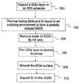
- FIG. 10shows the invention in flowchart form. More specifically, the invention first deposits a SiGe layer on an SOI wafer 300 . Next, the invention performs thermal mixing of the SiGe and Si layers 302 to form a partially relaxed SiGe on insulator. As mentioned above, the process of thermally mixing the SiGe and Si layers comprises heating the SiGe layer to approximately 1200° C.-1300° C. in an oxidizing environment. The invention then removes the oxide on SGOI using an HF etch 304 . A non-selective SiGe thinning process is then carried out to reduce the SiGe thickness down to the desired thickness 306 . This keeps the Ge concentration and the amount of relaxation unchanged regardless of the thickness of the SiGe layer.
- the SiGe surfaceis smoothed 308 . This way, the invention is able to obtain a thin SGOI film with high relaxation, and with low stacking fault defect density. Finally, the invention deposits Si on the thin SGOI wafer 310 .
- the present inventionis applicable to the manufacture of high-performance semiconductor devices which include SGOI films.
- the inventionhas been described in terms of a full process of making thick SGOI by thermal mixing and thinning the thick SGOI to obtain a thin SGOI with high relaxation and low stacking fault defect density.
- the SiGe thinning and smoothing techniques described in this inventioncan be applied to pre-formed SGOI wafers, such as SGOI wafers formed by film transferring technique.
- film transferring techniquesa partially or fully relaxed SiGe layer is first formed on a first wafer, and then transferred to a carrier wafer using wafer bonding, and an insulator layer is formed between the SiGe layer and the carrier wafer.
Landscapes
- Engineering & Computer Science (AREA)
- Microelectronics & Electronic Packaging (AREA)
- Condensed Matter Physics & Semiconductors (AREA)
- General Physics & Mathematics (AREA)
- Manufacturing & Machinery (AREA)
- Computer Hardware Design (AREA)
- Physics & Mathematics (AREA)
- Power Engineering (AREA)
- Chemical & Material Sciences (AREA)
- Materials Engineering (AREA)
- Recrystallisation Techniques (AREA)
- Drying Of Semiconductors (AREA)
- Formation Of Insulating Films (AREA)
Abstract
Description
Claims (11)
Applications Claiming Priority (1)
| Application Number | Priority Date | Filing Date | Title |
|---|---|---|---|
| PCT/US2004/001555WO2005078786A1 (en) | 2004-01-16 | 2004-01-16 | Method of forming thin sgoi wafers with high relaxation and low stacking fault defect density |
Publications (2)
| Publication Number | Publication Date |
|---|---|
| US20070128840A1 US20070128840A1 (en) | 2007-06-07 |
| US7550370B2true US7550370B2 (en) | 2009-06-23 |
Family
ID=34862309
Family Applications (1)
| Application Number | Title | Priority Date | Filing Date |
|---|---|---|---|
| US10/597,066Expired - Fee RelatedUS7550370B2 (en) | 2004-01-16 | 2004-01-16 | Method of forming thin SGOI wafers with high relaxation and low stacking fault defect density |
Country Status (7)
| Country | Link |
|---|---|
| US (1) | US7550370B2 (en) |
| EP (1) | EP1709671B1 (en) |
| JP (1) | JP4686480B2 (en) |
| KR (1) | KR100925310B1 (en) |
| CN (1) | CN100459072C (en) |
| AT (1) | ATE552611T1 (en) |
| WO (1) | WO2005078786A1 (en) |
Cited By (9)
| Publication number | Priority date | Publication date | Assignee | Title |
|---|---|---|---|---|
| US20110032541A1 (en)* | 2008-07-30 | 2011-02-10 | Nireco Corporation | Film thickness measuring device and film thickness measuring method |
| US9324843B2 (en) | 2014-09-05 | 2016-04-26 | International Business Machines Corporation | High germanium content silicon germanium fins |
| US9362311B1 (en) | 2015-07-24 | 2016-06-07 | Samsung Electronics Co., Ltd. | Method of fabricating semiconductor device |
| US9530669B1 (en)* | 2015-11-30 | 2016-12-27 | International Business Machines Corporation | Method of making a semiconductor device having a semiconductor material on a relaxed semiconductor including replacing a strained, selective etchable material, with a low density dielectric in a cavity |
| US9570298B1 (en) | 2015-12-09 | 2017-02-14 | International Business Machines Corporation | Localized elastic strain relaxed buffer |
| US9577043B2 (en) | 2014-10-10 | 2017-02-21 | Samsung Electronics Co., Ltd. | Semiconductor device and method for fabricating the same |
| US9698244B2 (en) | 2015-04-10 | 2017-07-04 | Samsung Electronics Co., Ltd. | Semiconductor devices and methods of fabricating the same |
| US9818761B2 (en) | 2015-06-25 | 2017-11-14 | International Business Machines Corporation | Selective oxidation for making relaxed silicon germanium on insulator structures |
| US10236205B2 (en)* | 2013-03-29 | 2019-03-19 | Jinan Jingzheng Electronics Co., Ltd. | Thin film and method for manufacturing thin film |
Families Citing this family (21)
| Publication number | Priority date | Publication date | Assignee | Title |
|---|---|---|---|---|
| FR2773261B1 (en) | 1997-12-30 | 2000-01-28 | Commissariat Energie Atomique | METHOD FOR THE TRANSFER OF A THIN FILM COMPRISING A STEP OF CREATING INCLUSIONS |
| US7550370B2 (en)* | 2004-01-16 | 2009-06-23 | International Business Machines Corporation | Method of forming thin SGOI wafers with high relaxation and low stacking fault defect density |
| JP2006080278A (en)* | 2004-09-09 | 2006-03-23 | Toshiba Ceramics Co Ltd | Strained silicon wafer and manufacturing method thereof |
| EP1763069B1 (en) | 2005-09-07 | 2016-04-13 | Soitec | Method for forming a semiconductor heterostructure |
| FR2891281B1 (en)* | 2005-09-28 | 2007-12-28 | Commissariat Energie Atomique | METHOD FOR MANUFACTURING A THIN FILM ELEMENT |
| US20070154637A1 (en)* | 2005-12-19 | 2007-07-05 | Rohm And Haas Electronic Materials Llc | Organometallic composition |
| DE102006020825A1 (en)* | 2006-05-04 | 2007-11-08 | Siltronic Ag | Process for producing a layered structure |
| JP5018066B2 (en)* | 2006-12-19 | 2012-09-05 | 信越半導体株式会社 | Method for manufacturing strained Si substrate |
| CN101388331B (en)* | 2008-10-31 | 2010-08-25 | 上海新傲科技股份有限公司 | Internal heating oxidation method for preparing silicon material on isolator |
| DE102009010883B4 (en)* | 2009-02-27 | 2011-05-26 | Amd Fab 36 Limited Liability Company & Co. Kg | Adjusting a non-silicon content in a semiconductor alloy during FET transistor fabrication by an intermediate oxidation process |
| FR2947098A1 (en) | 2009-06-18 | 2010-12-24 | Commissariat Energie Atomique | METHOD OF TRANSFERRING A THIN LAYER TO A TARGET SUBSTRATE HAVING A THERMAL EXPANSION COEFFICIENT DIFFERENT FROM THAT OF THE THIN LAYER |
| US20110086444A1 (en)* | 2009-10-14 | 2011-04-14 | Taiwan Semiconductor Manufacturing Company, Ltd. | Process for producing substrates free of patterns using an alpha stepper to ensure results |
| US8703551B2 (en)* | 2011-05-06 | 2014-04-22 | Globalfoundries Inc. | Process flow to reduce hole defects in P-active regions and to reduce across-wafer threshold voltage scatter |
| JP2013055231A (en)* | 2011-09-05 | 2013-03-21 | Shin Etsu Handotai Co Ltd | Epitaxial wafer manufacturing method |
| CN102290369B (en)* | 2011-09-22 | 2013-12-04 | 中国科学院上海微系统与信息技术研究所 | Thin GOI (germanium-on-insulator) wafer and preparation method thereof |
| US8883598B2 (en)* | 2012-03-05 | 2014-11-11 | Taiwan Semiconductor Manufacturing Co., Ltd. | Thin capped channel layers of semiconductor devices and methods of forming the same |
| US9608067B2 (en)* | 2015-03-30 | 2017-03-28 | International Business Machines Corporation | Hybrid aspect ratio trapping |
| CN106257631A (en)* | 2015-06-18 | 2016-12-28 | 中芯国际集成电路制造(上海)有限公司 | A kind of semiconductor device and manufacture method, electronic installation |
| FR3061803B1 (en)* | 2017-01-11 | 2019-08-16 | Soitec | FRONT-SIDE TYPE IMAGE SENSOR SUBSTRATE AND METHOD OF MANUFACTURING SUCH A SUBSTRATE |
| FR3061988B1 (en)* | 2017-01-13 | 2019-11-01 | Soitec | SURFACE MELTING METHOD OF SEMICONDUCTOR SUBSTRATE ON INSULATION |
| CN111551762A (en)* | 2020-05-14 | 2020-08-18 | 中国电子科技集团公司第二十四研究所 | Germanium epitaxial layer defect density detection method based on in-situ corrosion |
Citations (12)
| Publication number | Priority date | Publication date | Assignee | Title |
|---|---|---|---|---|
| US4409260A (en)* | 1979-08-15 | 1983-10-11 | Hughes Aircraft Company | Process for low-temperature surface layer oxidation of a semiconductor substrate |
| US5698869A (en) | 1994-09-13 | 1997-12-16 | Kabushiki Kaisha Toshiba | Insulated-gate transistor having narrow-bandgap-source |
| US6066576A (en)* | 1997-06-04 | 2000-05-23 | Micron Technology, Inc. | Method for forming oxide using high pressure |
| US6117750A (en) | 1997-12-29 | 2000-09-12 | France Telecom | Process for obtaining a layer of single-crystal germanium or silicon on a substrate of single-crystal silicon or germanium, respectively |
| US20020185686A1 (en) | 2001-06-12 | 2002-12-12 | International Business Machines Corporation | Relaxed SiGe layers on Si or silicon-on-insulator substrates by ion implantation and thermal annealing |
| US20030013280A1 (en)* | 2000-12-08 | 2003-01-16 | Hideo Yamanaka | Semiconductor thin film forming method, production methods for semiconductor device and electrooptical device, devices used for these methods, and semiconductor device and electrooptical device |
| US6551889B2 (en) | 2000-01-27 | 2003-04-22 | Sige Semiconductor, Inc. | Method of producing a SI-GE base heterojunction bipolar device |
| US20030089901A1 (en) | 2001-03-02 | 2003-05-15 | Fitzgerald Eugene A. | Relaxed silicon germanium platform for high speed cmos electronics and high speed analog circuits |
| US20040242006A1 (en)* | 2003-05-30 | 2004-12-02 | International Business Machines Corporation | SiGe lattice engineering using a combination of oxidation, thinning and epitaxial regrowth |
| US20040241460A1 (en)* | 2003-05-30 | 2004-12-02 | International Business Machines Corporation | Formation of silicon-Germanium-on-insulator (SGOI) by an integral high temperature SIMOX-Ge interdiffusion anneal |
| US20060054891A1 (en)* | 2004-09-13 | 2006-03-16 | International Business Machines Corporation | Method of creating defect free high Ge content (>25%) SiGe-on-insulator (SGOI) substrates using wafer bonding techniques |
| US20070128840A1 (en)* | 2004-01-16 | 2007-06-07 | International Business Machines Corporation | Method of forming thin sgoi wafers with high relaxation and low stacking fault defect density |
Family Cites Families (15)
| Publication number | Priority date | Publication date | Assignee | Title |
|---|---|---|---|---|
| US5298457A (en)* | 1993-07-01 | 1994-03-29 | G. I. Corporation | Method of making semiconductor devices using epitaxial techniques to form Si/Si-Ge interfaces and inverting the material |
| US5906951A (en)* | 1997-04-30 | 1999-05-25 | International Business Machines Corporation | Strained Si/SiGe layers on insulator |
| JP3884203B2 (en)* | 1998-12-24 | 2007-02-21 | 株式会社東芝 | Manufacturing method of semiconductor device |
| JP2001351869A (en)* | 2000-06-09 | 2001-12-21 | Mitsubishi Materials Silicon Corp | Silicon wafer and manufacturing method |
| US6524935B1 (en)* | 2000-09-29 | 2003-02-25 | International Business Machines Corporation | Preparation of strained Si/SiGe on insulator by hydrogen induced layer transfer technique |
| US6890835B1 (en)* | 2000-10-19 | 2005-05-10 | International Business Machines Corporation | Layer transfer of low defect SiGe using an etch-back process |
| US6448152B1 (en) | 2001-02-20 | 2002-09-10 | Silicon Genesis Corporation | Method and system for generating a plurality of donor wafers and handle wafers prior to an order being placed by a customer |
| JP2002289533A (en)* | 2001-03-26 | 2002-10-04 | Kentaro Sawano | Method for polishing surface of semiconductor, method for fabricating semiconductor device and semiconductor device |
| US6660607B2 (en)* | 2001-03-30 | 2003-12-09 | International Business Machines Corporation | Method for fabricating heterojunction bipolar transistors |
| US20020168802A1 (en)* | 2001-05-14 | 2002-11-14 | Hsu Sheng Teng | SiGe/SOI CMOS and method of making the same |
| JP4378904B2 (en)* | 2001-09-28 | 2009-12-09 | 株式会社Sumco | Manufacturing method of semiconductor substrate and manufacturing method of field effect transistor |
| JP2003158250A (en)* | 2001-10-30 | 2003-05-30 | Sharp Corp | SiGe / SOI CMOS and manufacturing method thereof |
| US6805962B2 (en)* | 2002-01-23 | 2004-10-19 | International Business Machines Corporation | Method of creating high-quality relaxed SiGe-on-insulator for strained Si CMOS applications |
| JP2004363199A (en)* | 2003-06-02 | 2004-12-24 | Sumitomo Mitsubishi Silicon Corp | Process for producing semiconductor substrate |
| JP4037803B2 (en)* | 2003-07-24 | 2008-01-23 | 株式会社東芝 | Method for manufacturing SGOI substrate |
- 2004
- 2004-01-16USUS10/597,066patent/US7550370B2/ennot_activeExpired - Fee Related
- 2004-01-16ATAT04703076Tpatent/ATE552611T1/enactive
- 2004-01-16CNCNB2004800405182Apatent/CN100459072C/ennot_activeExpired - Fee Related
- 2004-01-16EPEP04703076Apatent/EP1709671B1/ennot_activeExpired - Lifetime
- 2004-01-16JPJP2006549218Apatent/JP4686480B2/ennot_activeExpired - Fee Related
- 2004-01-16WOPCT/US2004/001555patent/WO2005078786A1/enactiveApplication Filing
- 2004-01-16KRKR1020067013849Apatent/KR100925310B1/ennot_activeExpired - Fee Related
Patent Citations (22)
| Publication number | Priority date | Publication date | Assignee | Title |
|---|---|---|---|---|
| US4409260A (en)* | 1979-08-15 | 1983-10-11 | Hughes Aircraft Company | Process for low-temperature surface layer oxidation of a semiconductor substrate |
| US5698869A (en) | 1994-09-13 | 1997-12-16 | Kabushiki Kaisha Toshiba | Insulated-gate transistor having narrow-bandgap-source |
| US6066576A (en)* | 1997-06-04 | 2000-05-23 | Micron Technology, Inc. | Method for forming oxide using high pressure |
| US6271152B1 (en)* | 1997-06-04 | 2001-08-07 | Micron Technology, Inc. | Method for forming oxide using high pressure |
| US6117750A (en) | 1997-12-29 | 2000-09-12 | France Telecom | Process for obtaining a layer of single-crystal germanium or silicon on a substrate of single-crystal silicon or germanium, respectively |
| US6429098B1 (en) | 1997-12-29 | 2002-08-06 | FRANCE TéLéCOM | Process for obtaining a layer of single-crystal germanium or silicon on a substrate of single-crystal silicon or germanium, respectively, and multilayer products obtained |
| US6551889B2 (en) | 2000-01-27 | 2003-04-22 | Sige Semiconductor, Inc. | Method of producing a SI-GE base heterojunction bipolar device |
| US7183229B2 (en)* | 2000-12-08 | 2007-02-27 | Sony Corporation | Semiconductor thin film forming method, production methods for semiconductor device and electrooptical device, devices used for these methods, and semiconductor device and electrooptical device |
| US20030013280A1 (en)* | 2000-12-08 | 2003-01-16 | Hideo Yamanaka | Semiconductor thin film forming method, production methods for semiconductor device and electrooptical device, devices used for these methods, and semiconductor device and electrooptical device |
| US20070087492A1 (en)* | 2000-12-08 | 2007-04-19 | Hideo Yamanaka | Method for forming semiconductor film, method for manufacturing semiconductor device and electrooptic device, apparatus for performing the same, and semiconductor device and electrooptic device |
| US20030089901A1 (en) | 2001-03-02 | 2003-05-15 | Fitzgerald Eugene A. | Relaxed silicon germanium platform for high speed cmos electronics and high speed analog circuits |
| US20020185686A1 (en) | 2001-06-12 | 2002-12-12 | International Business Machines Corporation | Relaxed SiGe layers on Si or silicon-on-insulator substrates by ion implantation and thermal annealing |
| US20040242006A1 (en)* | 2003-05-30 | 2004-12-02 | International Business Machines Corporation | SiGe lattice engineering using a combination of oxidation, thinning and epitaxial regrowth |
| US20050153487A1 (en)* | 2003-05-30 | 2005-07-14 | International Business Machines Corporation | Formation of silicon-germanium-on-insulator (SGOI) by an integral high temperature simox-Ge interdiffusion anneal |
| US7026249B2 (en)* | 2003-05-30 | 2006-04-11 | International Business Machines Corporation | SiGe lattice engineering using a combination of oxidation, thinning and epitaxial regrowth |
| US7084050B2 (en)* | 2003-05-30 | 2006-08-01 | International Business Machines Corporation | Formation of silicon-germanium-on-insulator (SGOI) by an integral high temperature SIMOX-Ge interdiffusion anneal |
| US6861158B2 (en)* | 2003-05-30 | 2005-03-01 | International Business Machines Corporation | Formation of silicon-germanium-on-insulator (SGOI) by an integral high temperature SIMOX-Ge interdiffusion anneal |
| US20040241460A1 (en)* | 2003-05-30 | 2004-12-02 | International Business Machines Corporation | Formation of silicon-Germanium-on-insulator (SGOI) by an integral high temperature SIMOX-Ge interdiffusion anneal |
| US20070128840A1 (en)* | 2004-01-16 | 2007-06-07 | International Business Machines Corporation | Method of forming thin sgoi wafers with high relaxation and low stacking fault defect density |
| US20060054891A1 (en)* | 2004-09-13 | 2006-03-16 | International Business Machines Corporation | Method of creating defect free high Ge content (>25%) SiGe-on-insulator (SGOI) substrates using wafer bonding techniques |
| US7235812B2 (en)* | 2004-09-13 | 2007-06-26 | International Business Machines Corporation | Method of creating defect free high Ge content (>25%) SiGe-on-insulator (SGOI) substrates using wafer bonding techniques |
| US20070218647A1 (en)* | 2004-09-13 | 2007-09-20 | International Business Machines Corporation | METHOD OF CREATING DEFECT FREE HIGH Ge CONTENT (> 25%) SiGe-ON-INSULATOR (SGOI) SUBSTRATES USING WAFER BONDING TECHNIQUES |
Cited By (11)
| Publication number | Priority date | Publication date | Assignee | Title |
|---|---|---|---|---|
| US20110032541A1 (en)* | 2008-07-30 | 2011-02-10 | Nireco Corporation | Film thickness measuring device and film thickness measuring method |
| US10236205B2 (en)* | 2013-03-29 | 2019-03-19 | Jinan Jingzheng Electronics Co., Ltd. | Thin film and method for manufacturing thin film |
| US9324843B2 (en) | 2014-09-05 | 2016-04-26 | International Business Machines Corporation | High germanium content silicon germanium fins |
| US9812530B2 (en) | 2014-09-05 | 2017-11-07 | International Business Machines Corporation | High germanium content silicon germanium fins |
| US9577043B2 (en) | 2014-10-10 | 2017-02-21 | Samsung Electronics Co., Ltd. | Semiconductor device and method for fabricating the same |
| US9698244B2 (en) | 2015-04-10 | 2017-07-04 | Samsung Electronics Co., Ltd. | Semiconductor devices and methods of fabricating the same |
| US9818761B2 (en) | 2015-06-25 | 2017-11-14 | International Business Machines Corporation | Selective oxidation for making relaxed silicon germanium on insulator structures |
| US9362311B1 (en) | 2015-07-24 | 2016-06-07 | Samsung Electronics Co., Ltd. | Method of fabricating semiconductor device |
| US9530669B1 (en)* | 2015-11-30 | 2016-12-27 | International Business Machines Corporation | Method of making a semiconductor device having a semiconductor material on a relaxed semiconductor including replacing a strained, selective etchable material, with a low density dielectric in a cavity |
| US9570298B1 (en) | 2015-12-09 | 2017-02-14 | International Business Machines Corporation | Localized elastic strain relaxed buffer |
| US9799513B2 (en) | 2015-12-09 | 2017-10-24 | International Business Machines Corporation | Localized elastic strain relaxed buffer |
Also Published As
| Publication number | Publication date |
|---|---|
| WO2005078786A1 (en) | 2005-08-25 |
| ATE552611T1 (en) | 2012-04-15 |
| CN1906742A (en) | 2007-01-31 |
| EP1709671A4 (en) | 2010-06-16 |
| KR100925310B1 (en) | 2009-11-04 |
| KR20060123471A (en) | 2006-12-01 |
| EP1709671A1 (en) | 2006-10-11 |
| US20070128840A1 (en) | 2007-06-07 |
| EP1709671B1 (en) | 2012-04-04 |
| JP4686480B2 (en) | 2011-05-25 |
| CN100459072C (en) | 2009-02-04 |
| JP2007518264A (en) | 2007-07-05 |
Similar Documents
| Publication | Publication Date | Title |
|---|---|---|
| US7550370B2 (en) | Method of forming thin SGOI wafers with high relaxation and low stacking fault defect density | |
| US7416909B2 (en) | Methods for preserving strained semiconductor substrate layers during CMOS processing | |
| US7439164B2 (en) | Methods of fabricating semiconductor structures having epitaxially grown source and drain elements | |
| CN101207016B (en) | Semiconductor heterostructure | |
| EP3739620B1 (en) | A silicon germanium-on-insulator structure | |
| US7022593B2 (en) | SiGe rectification process | |
| US7495266B2 (en) | Strained silicon-on-silicon by wafer bonding and layer transfer | |
| JP2701793B2 (en) | Method for manufacturing semiconductor device | |
| JP2003318110A (en) | Semiconductor substrate and its manufacturing method, semiconductor device manufacturing method | |
| US20050280081A1 (en) | Semiconductor devices having bonded interfaces and methods for making the same | |
| US7790566B2 (en) | Semiconductor surface treatment for epitaxial growth | |
| JP2006253605A (en) | Semiconductor substrate, semiconductor device, and manufacturing method thereof |
Legal Events
| Date | Code | Title | Description |
|---|---|---|---|
| AS | Assignment | Owner name:INTERNATIONAL BUSINESS MACHINES CORPORATION, NEW Y Free format text:ASSIGNMENT OF ASSIGNORS INTEREST;ASSIGNORS:CHEN, HUAJIE;BEDELL, STEPHEN W.;SADANA, DEVENDRA K.;AND OTHERS;REEL/FRAME:015003/0210 Effective date:20031218 | |
| AS | Assignment | Owner name:INTERNATIONAL BUSINESS MACHINES CORPORATION, NEW Y Free format text:ASSIGNMENT OF ASSIGNORS INTEREST;ASSIGNORS:CHEN, HUAJIE;BEDELL, STEPHEN W.;SADANA, DEVENDRA K.;AND OTHERS;REEL/FRAME:017945/0581;SIGNING DATES FROM 20060621 TO 20060706 | |
| FEPP | Fee payment procedure | Free format text:PAYOR NUMBER ASSIGNED (ORIGINAL EVENT CODE: ASPN); ENTITY STATUS OF PATENT OWNER: LARGE ENTITY | |
| REMI | Maintenance fee reminder mailed | ||
| FPAY | Fee payment | Year of fee payment:4 | |
| SULP | Surcharge for late payment | ||
| AS | Assignment | Owner name:GLOBALFOUNDRIES U.S. 2 LLC, NEW YORK Free format text:ASSIGNMENT OF ASSIGNORS INTEREST;ASSIGNOR:INTERNATIONAL BUSINESS MACHINES CORPORATION;REEL/FRAME:036550/0001 Effective date:20150629 | |
| AS | Assignment | Owner name:GLOBALFOUNDRIES INC., CAYMAN ISLANDS Free format text:ASSIGNMENT OF ASSIGNORS INTEREST;ASSIGNORS:GLOBALFOUNDRIES U.S. 2 LLC;GLOBALFOUNDRIES U.S. INC.;REEL/FRAME:036779/0001 Effective date:20150910 | |
| REMI | Maintenance fee reminder mailed | ||
| LAPS | Lapse for failure to pay maintenance fees | ||
| STCH | Information on status: patent discontinuation | Free format text:PATENT EXPIRED DUE TO NONPAYMENT OF MAINTENANCE FEES UNDER 37 CFR 1.362 | |
| FP | Lapsed due to failure to pay maintenance fee | Effective date:20170623 | |
| AS | Assignment | Owner name:GLOBALFOUNDRIES U.S. INC., NEW YORK Free format text:RELEASE BY SECURED PARTY;ASSIGNOR:WILMINGTON TRUST, NATIONAL ASSOCIATION;REEL/FRAME:056987/0001 Effective date:20201117 |