US7549209B2 - Method of fabricating a magnetic discrete track recording disk - Google Patents
Method of fabricating a magnetic discrete track recording diskDownload PDFInfo
- Publication number
- US7549209B2 US7549209B2US11/040,519US4051905AUS7549209B2US 7549209 B2US7549209 B2US 7549209B2US 4051905 AUS4051905 AUS 4051905AUS 7549209 B2US7549209 B2US 7549209B2
- Authority
- US
- United States
- Prior art keywords
- layer
- substrate
- zones
- embossable
- nip
- Prior art date
- Legal status (The legal status is an assumption and is not a legal conclusion. Google has not performed a legal analysis and makes no representation as to the accuracy of the status listed.)
- Expired - Fee Related, expires
Links
Images


Classifications
- G—PHYSICS
- G11—INFORMATION STORAGE
- G11B—INFORMATION STORAGE BASED ON RELATIVE MOVEMENT BETWEEN RECORD CARRIER AND TRANSDUCER
- G11B5/00—Recording by magnetisation or demagnetisation of a record carrier; Reproducing by magnetic means; Record carriers therefor
- G11B5/84—Processes or apparatus specially adapted for manufacturing record carriers
- G11B5/8404—Processes or apparatus specially adapted for manufacturing record carriers manufacturing base layers
- G—PHYSICS
- G11—INFORMATION STORAGE
- G11B—INFORMATION STORAGE BASED ON RELATIVE MOVEMENT BETWEEN RECORD CARRIER AND TRANSDUCER
- G11B5/00—Recording by magnetisation or demagnetisation of a record carrier; Reproducing by magnetic means; Record carriers therefor
- G11B5/84—Processes or apparatus specially adapted for manufacturing record carriers
- G11B5/855—Coating only part of a support with a magnetic layer
- G—PHYSICS
- G11—INFORMATION STORAGE
- G11B—INFORMATION STORAGE BASED ON RELATIVE MOVEMENT BETWEEN RECORD CARRIER AND TRANSDUCER
- G11B5/00—Recording by magnetisation or demagnetisation of a record carrier; Reproducing by magnetic means; Record carriers therefor
- G11B5/84—Processes or apparatus specially adapted for manufacturing record carriers
- G11B5/858—Producing a magnetic layer by electro-plating or electroless plating
- Y—GENERAL TAGGING OF NEW TECHNOLOGICAL DEVELOPMENTS; GENERAL TAGGING OF CROSS-SECTIONAL TECHNOLOGIES SPANNING OVER SEVERAL SECTIONS OF THE IPC; TECHNICAL SUBJECTS COVERED BY FORMER USPC CROSS-REFERENCE ART COLLECTIONS [XRACs] AND DIGESTS
- Y10—TECHNICAL SUBJECTS COVERED BY FORMER USPC
- Y10T—TECHNICAL SUBJECTS COVERED BY FORMER US CLASSIFICATION
- Y10T29/00—Metal working
- Y10T29/49—Method of mechanical manufacture
- Y10T29/49002—Electrical device making
- Y10T29/4902—Electromagnet, transformer or inductor
- Y10T29/49021—Magnetic recording reproducing transducer [e.g., tape head, core, etc.]
- Y10T29/49025—Making disc drive
Definitions
- Embodiments of this inventionrelate to the field of disk drives and, more specifically, to disks used in disk drive systems.
- a disk drive systemincludes one or more magnetic recording disks and control mechanisms for storing data on the disks.
- the disksare constructed of a substrate, that may be textured, and multiple film layers. In most systems, an aluminum-based substrate is used. However, alternative substrate materials such as glass have various performance benefits such that it may be desirable to use a glass substrate.
- One of the film layers on a diskis a magnetic layer used to store data. The reading and writing of data is accomplished by flying a read-write head over the disk to alter the properties of the disk's magnetic layer.
- the read-write headis typically a part of or affixed to a larger body that flies over the disk, referred to as a slider.
- Recording densityis a measure of the amount of data that may be stored in a given area of a disk.
- MRmagneto-resistive
- GMRgiant magneto-resistive
- DTRdiscrete track recording
- Such recessed zonesmay also store servo information.
- the recessed zonesseparate the raised zones from one another to inhibit or prevent the unintended storage of data in the recessed zones.
- DTR magnetic recording disksmay not have a desired “preferred” circumferential orientation of magnetic material in their magnetic recording films.
- “Preferred” circumferential orientation of the magnetic mediaaids in achieving optimal signal-to-noise ratio (SNR) and resolution to obtain the best possible performance from the magnetic media.
- SNRsignal-to-noise ratio
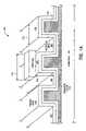
- FIG. 1Aillustrates a cross-sectional perspective view of one embodiment of a patterned disk and a write element of a head.
- FIG. 1Billustrates a cross-sectional perspective view of an alternative embodiment of a patterned disk.
- FIGS. 2A-2Gshow expanded cross sectional views illustrating an exemplary embodiment of a method of forming a discrete track recording pattern on a nickel-phosphorus layer.
- FIGS. 3A-3Fshow expanded cross sectional views illustrating another exemplary embodiment of a method of forming a discrete track recording pattern on a nickel-phosphorus layer.
- FIGS. 4A-4Gshow expanded cross sectional views illustrating an exemplary embodiment of a method of forming a discrete track recording pattern on a substrate.
- FIGS. 5A-5Fshow expanded cross sectional views illustrating another exemplary embodiment of a method of forming a discrete track recording pattern on a substrate.
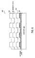
- FIG. 6is a cross section illustrating one embodiment of a recording disk having a patterned nickel-phosphorus layer.
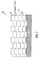
- FIG. 7is a cross section illustrating one embodiment of a recording disk having a patterned substrate.
- FIGS. 8A-8Bshow expanded cross sectional views illustrating an exemplary embodiment of a method of depositing a soft magnetic underlayer on a patterned substrate.
- FIG. 9is a cross section illustrating one embodiment of a recording disk having a soft magnetic underlayer deposited on a patterned substrate.
- FIG. 10illustrates one embodiment of a disk drive.
- one layer deposited or disposed above or below another layermay be directly in contact with the other layer or may have one or more intervening layers.
- one layer deposited or disposed between layersmay be directly in contact with the layers or may have one or more intervening layers.
- the apparatus and methods discussed hereinmay be used with various types of disks.
- the apparatus and methods discussed hereinmay be used with a magnetic recording disk.
- the apparatus and methods discussed hereinmay be used with other types of digital recording disks, for example, optical recording disks such as a compact disc (CD) and a digital-versatile-disk (DVD).
- CDcompact disc
- DVDdigital-versatile-disk
- a longitudinal magnetic recording disk having a nickel-phosphorus (NiP) underlayer with a discrete track recording patternis described.
- the discrete track recording patternprovides inter-track isolation within the NiP layer.
- the recording diskhas a substrate, a NiP layer disposed above the substrate and a magnetic recording layer disposed above the NiP layer.
- methods for patterning a NiP layer with a discrete track recording patternare described.
- the NiP layer, continuous throughout the discrete track recording pattern,may initially be imprinted with a stamper that forms an intermediate pattern relative the final discrete track recording pattern.
- a method of forming the discrete track recording patterninvolves etching (e.g., plasma, e-beam, chemical) the NiP layer in which portions of the NiP layer are removed to form the raised and recessed zones (e.g., data and non-data zones of a DTR pattern).
- etchinge.g., plasma, e-beam, chemical
- an additive processmay be used in which a material compatible with the NiP layer may be plated up on the NiP layer to form the discrete track recording pattern.
- the discrete track recording patterndoes not extend down into the disk substrate.
- a discrete track recording patternis formed in the substrate.
- the patterned substratemay be formed analogous to the subtractive or additive process for patterning the NiP layer.
- FIG. 1Aillustrates a cross-sectional perspective view of a patterned disk and a write element of a head.
- the disk 100includes multiple film layers that have been omitted for clarity of the following discussion.
- reading and writing of data on the disk 100is accomplished by flying, for example, a read-write head 110 over the disk 100 to alter the properties of the disk's magnetic layer 150 .
- the head 110is centered above a track of the rotating disk 100 .
- the recording head 110may be, for example, a dual element head having a read element for performing a read operation and a write element for performing a write operation.
- the disk 100includes a substrate 120 that may be textured, and multiple film layers disposed above the substrate 120 .
- the disks described hereinmay be manufactured with, by example, a glass substrate or a metal/metal alloy substrate.
- Glass substrates that may be usedinclude, for example, a silica containing glass such as borosilicate glass and aluminosilicate glass.
- Metal alloy substrates that may be usedinclude, for example, aluminum-magnesium (AlMg) substrates. In an alternative embodiment, other substrate materials including polymers and ceramics may be used.
- the multiple film layersinclude a NiP layer 130 and magnetic layer 150 .
- a discrete track recording patternis formed into the NiP layer 130 as discussed further below.
- a magnetic layer 150is disposed above the NiP layer 130 .
- the DTR patternincludes recessed zones 160 and raised zones 170 .
- the recessed zones 160have a depth 165 relative to the recording head 110 and/or raised zones 170 .
- the width 115 of the head 110is greater than the width 175 of the raised zones 170 such that portions of the head 110 extend over the recessed zones 160 during operation.
- the recessed zones 160are sufficiently separated by a distance 165 from the head 110 to inhibit storage of data by the head 110 in the magnetic layer 150 directly below the recessed zones 160 .
- the raised zones 170are sufficiently close to the head 110 to enable the writing of data in the magnetic layer 150 directly below the raised zones 170 .
- a width 175 of each raised zonemay be about 1250 angstroms ( ⁇ ) and a width of each recessed zone may be typically about 1 ⁇ 3 of the raised zone, or about 400 ⁇ .
- a depth 165 of each recessed zonemay be about 400 ⁇ .
- the raised and recessed zonesmay have a pitch between about 200-2000 ⁇ . Dimensions discussed above are exemplary and may have other values.
- the raised zones 170 of NiP layer 130correspond to the data tracks.
- Informationsuch as servo (head positioning) information may be stored in the recessed zones 160 .
- servo informationmay be interleaved with data in sectors on stored on the raised zones 170 .
- the raised zones 170 and recessed zones 160are typically formed as alternating concentric circles although other configurations (e.g., spiral) are contemplated.
- the recessed zones 160isolate the raised zones 170 (e.g., the data tracks) from one another, resulting in data tracks that are defined both physically and magnetically.
- the discrete track pattern formed in the NiP layer 130may include data islands as illustrated in FIG. 1B .
- Each of the data islands 190may hold a block of data (e.g., one bit or multiple bits) and are isolated form one another by the recessed zones.
- Such a configurationmay reduce the amount of noise (e.g., noise between tracks and between blocks of data or bits) that is sensed by the read head 110 .
- the recessed and raised zonesmay have alternate shapes that still isolate data blocks from recessed zones.
- a method to form a continuous NiP layer with a discrete track recording patternis described.
- the methodmay involve first imprinting an embossable layer disposed above the NiP layer followed by a subtractive or additive process to form the desired pattern.
- Imprinting the embossable layermay utilize lithography techniques, for example, nanoimprint lithography.
- FIGS. 2A-2Gshow expanded cross sectional views illustrating one embodiment of forming a discrete track recording pattern on a NiP layer of a longitudinal magnetic recording disk.
- the methodinvolves a subtractive process in which a layer or layers disposed on a disk substrate may be removed (e.g., through imprint lithography and etching) to expose a desired pattern on the NiP layer.
- the various layers illustrated in FIGS. 2A-2Gare exemplary and may not be scaled to representative sizes.
- the patterning processbegins with a disk-shaped substrate 205 .
- Disk substrate 205may be made of a number of materials including metals (e.g., aluminum), glass, silicon or other conventional disk substrate materials known in the art.
- substrate 205may be plated with a NiP layer 215 .
- NiP layer 215may be formed by electroplating, electroless plating, or by other methods known in the art.
- Plating disk substrate 205 with a rigid or metallic material such as NiPprovides mechanical support to disk substrate 205 for subsequent texturing, polishing, and/or patterning processes. Plating of disk substrate 205 may not be necessary, however, if disk substrate 205 is composed of a sufficiently rigid or hard material such as glass.
- NiP layer 215may be polished, for example, by a uniform etch. In alternative embodiments, other polishing techniques may be used. Polishing techniques are well known in the art; accordingly, a detailed discussion is not provided. Alternatively, NiP layer 215 may not be polished.
- NiP layer 215may be anisotropically textured with a pattern (e.g., cross-hatch, circumferential), by various methods such as mechanical texturing using fixed or free abrasive particles (e.g., diamond). Alternatively, other types of texturing methods, such as laser texturing, may be used.
- Certain types of texturing, on the intended data zones of a disk, before deposition of nucleation and magnetic layermay encourage preferred circumferential orientation of the magnetic media on a disk.
- Preferred circumferential orientation of the magnetic media on a diskaids in achieving optimal signal-to-noise (SNR) and resolution to obtain the best possible performance from the magnetic media.
- texturing of NiP layer 215may be performed after the discrete track recording pattern has been formed.
- disk substrate 205may then be coated with an embossable layer 220 , for example, a photoresist, an electron sensitive resist, or other embossable materials.
- embossable layer 220for example, a photoresist, an electron sensitive resist, or other embossable materials.
- Spin coating, dip coating, and spray coatingare just some methods of disposing embossable layer 220 on NiP layer 215 .
- Other coating methodssuch as sputtering and vacuum deposition (e.g., CVD) may be used.
- embossable layer materialssuch as dye polymer may be used for other examples, thermoplastics (e.g., amorphous, semi-crystalline, crystalline), thermosetting (e.g., epoxies, phenolics, polysiloxanes, ormosils, sol-gel) and radiation curable (e.g., UV curable, electron-beam curable) polymers.
- thermoplasticse.g., amorphous, semi-crystalline, crystalline
- thermosettinge.g., epoxies, phenolics, polysiloxanes, ormosils, sol-gel
- radiation curablee.g., UV curable, electron-beam curable
- embossable layer 220may have a thickness in the range of about 100-5000 ⁇ .
- Embossable layer 220may also be referred to as a “masking layer” and a “stencil layer.”
- embossable layer 220is imprinted with a pattern of recessed ( 222 , 224 , 226 ) and raised ( 221 , 223 , 225 ) zones.
- the stamping of embossable layer 220may utilize, for example, nanoimprint lithography techniques that are well known in the art.
- a stamper(not shown) bearing a discrete track recording pattern, may be used to imprint embossable layer 220 to form recessed zones ( 222 , 224 , 226 ) and raised zones ( 221 , 223 , 225 ).
- embossable layer 220Because of the thickness of the embossable layer 220 , the imprint of raised and recessed zones are not likely to press into NiP layer 215 . Alternatively, if embossable layer 220 is relatively thin, it may be stamped to leave very little embossable material in the recessed zones ( 222 , 224 , 226 ). Subsequently, embossable material in the recessed zones ( 222 , 224 , 226 ) may be removed to expose NiP layer 215 . The stamper used to pattern the embossable layer 220 has the inverse, or negative replica, of the desired pattern (i.e., the discrete track recording pattern on NiP layer 215 ) to be formed.
- the intermediate pattern in embossable layer 220may be etched to further define the alternating recessed zones ( 222 , 224 , 226 ) and raised zones ( 221 , 223 , 225 ) that form the basis for the discrete track recording pattern on NiP layer 215 .
- a series, or step-wise process of etching proceduresmay be performed on embossable layer 220 and NiP layer 215 to form the desired track pattern.
- Embossable layer 220serves as a stencil that exposes the NiP layer 215 in areas beneath the recessed zones ( 222 , 224 , 226 ) of the pattern formed by the stamper.
- plasma etchingis utilized to remove embossable layer 220 material in recessed zones ( 222 , 224 , 226 ) down to the NiP layer 215 .
- other etching methodsmay be used to remove embossable layer 220 material in at least the recessed zones, for example, using chemical etching, electron beam (e-beam) etching, ion-beam etching (passive or reactive) sputter etching, and plasma etching with reactive gases.
- embossable layer materialmay be removed from both the raised zones ( 221 , 223 , 225 ) and recessed zones ( 222 , 224 , 226 ) at approximately a similar rate.
- Chemical etchingwill remove the embossable layer 220 in both the recessed zones ( 222 , 224 , 226 ) and raised zones ( 221 , 223 , 225 ) until NiP layer 215 is exposed in the recessed zones ( 222 , 224 , 226 ), as illustrated by FIG. 2E .
- recessed zones ( 222 , 224 , 226 ) of NiP layer 215may be further etched (e.g., by chemical, e-beam, ion-beam, and sputter etching).
- the etching of recessed zones ( 222 , 224 , 226 )may not penetrate through NiP layer 215 to the disk substrate 205 such that NiP layer 215 forms a continuous pattern of recessed zones ( 222 , 224 , 226 ) and raised zones ( 221 , 223 , 225 ).
- the remaining embossable layer 220 on the raised zones ( 221 , 223 , 225 ) of the discrete track recording patternmay then be removed, for example, by the methods discussed above in relation to FIG. 2E , or by other methods such as polishing (e.g., fine, kiss, or coarse polishing).
- polishinge.g., fine, kiss, or coarse polishing
- the raised zones ( 221 , 223 , 225 ), corresponding to the data recording zones of the magnetic diskmay be textured, rather than texturing the entire NiP layer 215 prior to coating with embossable layer 220 as discussed above in relation to FIG. 2B .
- Any of the texturing methods described abovemay be used (e.g., mechanical and laser texturing).
- NiP layer 215may be textured earlier before any imprinting or etching (e.g., as described with respect to FIG. 2B , after NiP plating of disk substrate 205 ). It should also be noted that various cleaning and/or polishing operations may be performed between the stages discussed above.
- one or more polishing operationsmay be performed to remove asperities from the surface of one or more of the layers. Asperities residing on the surface of any layer may have negative effects on the performance of the manufactured disk.
- other layerse.g., a magnetic layer, lamination layer
- NiP layer 215may be disposed above NiP layer 215 to complete the disk manufacturing process.
- FIGS. 3A-3Fshow expanded cross sectional views illustrating an alternative embodiment of forming a discrete track recording pattern on a NiP layer of a longitudinal magnetic recording disk.
- This methodinvolves an additive process in which a material compatible or identical to material forming the initial NiP layer is added or plated to form the raised zones of the discrete track recording pattern.
- the various layers illustrated in FIGS. 3A-3Fare exemplary and not scaled to proper sizes so that the process of patterning the NiP layer may be described with clarity.
- FIGS. 3A-3Fare analogous to the subtractive process illustrated by FIGS. 2A-2G with respect to the stamping and etching of the embossable layer 320 disposed above NiP layer 315 .
- the processbegins with NiP layer 315 disposed on disk substrate 305 (e.g., by electro plating and electroless plating).
- the NiP plated disk substrate 305is not necessarily textured at this point. As will be apparent below, this method requires texturing of the final raised zones of NiP layer 315 after the discrete track recording pattern is formed.
- Disk substrate 305may be composed of materials similar to those discussed above with respect to the substrate 205 .
- disk substrate 305may then be coated with an embossable layer 320 , for example, a photoresist, an electron sensitive resist, or other embossable materials.
- an embossable layer 320for example, a photoresist, an electron sensitive resist, or other embossable materials.
- Spin coating, dip coating, and spray coatingare just some methods of disposing the embossable layer 320 on substrate 305 .
- thermoplasticse.g., amorphous, semi-crystalline, crystalline
- thermosettinge.g., epoxies, phenolics, polysiloxanes, ormosils, sol-gel
- radiation curable polymerse.g., UV curable, electron-beam curable
- a stamper(not shown) bearing a discrete track recording pattern, may be used to impress embossable layer 320 to form recessed zones ( 322 , 324 , 326 ) and raised zones ( 321 , 323 , 325 ). If the embossable layer 320 is thick relative to the depth of the pattern in the stamper, the imprint from the stamper is not likely to register deep enough to reach NiP layer 315 . Alternatively, if embossable layer 320 is relatively thin, it may be stamped to leave very little embossable material in the recessed zones ( 322 , 324 , 326 ).
- embossable material in the recessed zones ( 322 , 324 , 326 )may be removed to expose NiP layer 315 .
- the stamper used to pattern the embossable layer 320may have a pattern identical to the pattern to be formed on NiP layer 315 .
- embossable layer material in the recessed zones ( 322 , 324 , 326 )may be removed by a number of etching methods (e.g., by chemical, plasma, e-beam, ion-beam, or sputter etching), such that surface areas of NiP layer 315 are exposed.
- etching methodse.g., by chemical, plasma, e-beam, ion-beam, or sputter etching
- embossable layer materialmay be removed from both the raised zones ( 321 , 323 , 325 ) and recessed zones ( 322 , 324 , 326 ) at approximately a similar rate.
- Chemical etchingwill remove the embossable layer 320 in both the recessed zones ( 322 , 324 , 326 ) and raised zones ( 321 , 323 , 325 ) until NiP layer 315 is exposed in the recessed zones ( 322 , 324 , 326 ), as illustrated by FIG. 3D .
- recessed zones ( 322 , 324 , 326 )may be plated or deposited (e.g., electroplating) with a material identical to or compatible with NiP layer 315 , such that recessed zones ( 322 , 324 , 326 ) become filled to a level comparable to the top surface of raised zones ( 321 , 323 , 325 ).
- the remaining segments of embossable layer 320may be removed, for example, by chemical etching so that only NiP layer 315 remains.
- zones 322 , 324 , 326 that were once recessed zonesare now raised zones that form the data zones of the NiP layer 315 .
- zones 321 , 323 , 325 that formed the raised zonesare now the recessed zones positioned between raised data zones 322 , 324 , 326 of the DTR pattern as illustrated by FIG. 3F .
- raised zones 322 , 324 , 326 of FIG. 3Fmay be formed by first depositing a NiP material over the imprinted embossable layer 320 (e.g., at FIG. 3D ) by various deposition methods such as chemical vapor deposition (CVD), sputtering, and ion beam deposition.
- CVDchemical vapor deposition
- the embossable layer materialmay be selectively removed by any number of etching methods described herein (e.g., chemical etching). In doing so, any NiP material deposited above the embossable layer becomes “lifted off,” resulting in the raised zones ( 322 , 324 , 326 ) and recessed zones ( 321 , 323 , 325 ) of FIG. 3F .
- FIG. 3Fshows the final raised zones ( 322 , 324 , 326 ) textured.
- texturing NiP layer 315 prior to depositing embossable layer 320would not preserve the textured areas in the final raised zones ( 322 , 324 , 326 ).
- the texturing methods described abovemay be used (e.g., mechanical and laser texturing).
- various cleaning and/or polishing operationsmay be performed between the stages discussed above. For example, one or more polishing operations (e.g., fine/kiss, coarse) may be performed to remove asperities from the surface of one or more of the layers.
- polishing operationse.g., fine/kiss, coarse
- other layerse.g., a magnetic layer, lamination layer
- NiP layer 315may be disposed above NiP layer 315 to form a longitudinal or perpendicular magnetic recording disk.
- the process of forming a discrete track recording pattern illustrated in FIGS. 2A-2Gdiffers from the process illustrated and described in FIGS. 3A-3F in that the former forms the recessed zones of the NiP layer by etching into the NiP layer to remove material making up the NiP layer.
- the initial stamping of the embossable layerserves as a template corresponding to the raised and recessed zones.
- the initial recessed impressions formed by a stampere.g., recessed zones 322 , 324 , 326 shown in FIG. 3C
- the stamper utilized to form the impression shown in FIG. 3Cmay form wider recessed zones compared to the raised zones because ultimately, the recessed zones that become the raised data zones of the NiP layer should be wider than the recessed zones.
- FIGS. 4A-4Gshow expanded cross sectional views illustrating an exemplary embodiment of a method of forming a discrete track recording pattern on a substrate for a magnetic recording disk.
- the various layers illustrated in FIGS. 4A-4Gare exemplary and may not be scaled to representative sizes.
- materials such as glassmay be used for the disk's substrate.
- Substrate disks constructed of materials such as glassmay not have a NiP plating because the material itself provides mechanical support for subsequent texturing, polishing, and/or patterning processes. With such substrates the discrete track recording pattern may be formed directly in the substrate.
- the method of forming the DTR pattern in a substratemay be analogous to the subtractive method discussed above with respect to FIGS.
- the patterning processbegins with a disk-shaped (e.g., glass) substrate 405 .
- Disk substrate 405may then be polished and planarized.
- disk substrate 405may be polished, for example, by a uniform etch. In alternative embodiments, other polishing techniques may be used. Alternatively, disk substrate 405 may not be polished.
- disk substrate 405may be anisotropically textured with a pattern, by various methods as discussed above. Alternatively, as discussed below, texturing of disk substrate 405 may be performed after the discrete track recording pattern has been formed.
- disk substrate 405may then be coated with an embossable layer 420 , for example, with a photoresist, an electron sensitive resist, or other embossable materials.
- an embossable layer 420for example, with a photoresist, an electron sensitive resist, or other embossable materials.
- Spin coating, dip coating, and spray coatingare just some methods of disposing the embossable layer 420 on substrate 405 .
- Other coating methods and other embossable layer materialsas discussed above, may be used.
- embossable layer 420is imprinted with a pattern of recessed zones ( 422 , 424 , 426 ) and raised zones ( 421 , 423 , 425 ).
- the stamping of embossable layer 420may utilize, for example, nanoimprint lithography techniques that are well known in the art.
- a stamper(not shown) bearing a discrete track recording pattern, may be used to imprint embossable layer 420 to form recessed zones ( 422 , 424 , 426 ) and raised zones ( 421 , 423 , 425 ).
- the stamper used to pattern the embossable layer 420has the inverse, or negative replica, of the desired pattern (i.e., the discrete track recording pattern on substrate 405 ) to be formed.
- embossable layer 420may be etched to further define the alternating recessed zones ( 422 , 424 , 426 ) and raised zones ( 421 , 423 , 425 ) that form the basis for the discrete track recording pattern on substrate 405 .
- a series, or step-wise process of etching proceduresmay be performed on embossable layer 420 and substrate 405 to form the desired track pattern.
- Embossable layer 420serves as a stencil to expose the substrate 405 in areas beneath the recessed zones ( 422 , 424 , 426 ) of the pattern formed by the stamper.
- plasma etchingis utilized to remove embossable layer 420 material in recessed zones ( 422 , 424 , 426 ) down to the substrate 405 .
- other etching methodsmay be used to remove embossable layer 420 material in at least the recessed zones, for examples, chemical etching, electron beam (e-beam) etching, ion-beam etching (passive or reactive), sputter etching, and plasma etching with reactive gases.
- embossable layer materialmay be removed from both the raised zones ( 421 , 423 , 425 ) and recessed zones ( 422 , 424 , 426 ) at approximately a similar rate.
- Chemical etchingwill remove the embossable layer 420 in both the recessed zones ( 422 , 424 , 426 ) and raised zones ( 421 , 423 , 425 ) until substrate 405 is exposed in the recessed zones ( 422 , 424 , 426 ), as illustrated by FIG. 4E .
- recessed zones ( 422 , 424 , 426 ) of substrate 405may be further etched (e.g., by chemical, e-beam, ion-beam, and sputter etching).
- the etching of recessed zones ( 422 , 424 , 426 )may not penetrate completely through substrate 405 such that substrate 405 forms a continuous pattern of recessed zones ( 422 , 424 , 426 ) and raised zones ( 421 , 423 , 425 ).
- the remaining embossable layer 420 on the raised zones ( 421 , 423 , 425 ) of the discrete track recording patternmay then be removed, for example, by the methods discussed above in relation to FIG. 4E .
- the removal of embossable layer 420exposes the entire top surface of substrate 405 , as illustrated by FIG. 4G .
- raised zones ( 421 , 423 , 425 ), corresponding to the data recording zones of the magnetic diskmay be textured at this stage, rather than texturing the entire substrate 405 prior to coating with embossable layer 420 as discussed above in relation to FIG. 4B .
- the texturing methods described abovemay be used (e.g., mechanical and laser texturing).
- substrate 405may be textured before any imprinting or etching (e.g., as described with respect to FIG. 4B ).
- various cleaning and/or polishing operationsmay be performed between the various stages.
- layerse.g., a magnetic layer
- layersmay be disposed above substrate 405 to form a longitudinal or perpendicular magnetic recording disk.
- FIGS. 5A-5Fshow expanded cross sectional views illustrating an alternative embodiment of forming a discrete track recording pattern on a substrate of a magnetic recording disk. This method involves an additive process in which a material compatible or identical to material forming the substrate is added or plated to form the raised zones of the discrete track recording pattern.
- the various layers illustrated in FIGS. 5A-5Fare exemplary and not scaled to proper sizes so that the process of patterning the substrate may be described with clarity.
- FIGS. 5A-5Fis analogous to the subtractive process illustrated by FIGS. 4A-4G with respect to the stamping and etching of the embossable layer 520 disposed above substrate 505 .
- the processbegins with substrate 505 .
- substrate 505is not necessarily textured at this point.
- this methodrequires texturing of the final raised zones of substrate 505 after the discrete track recording pattern is formed
- disk substrate 505may then be coated with an embossable layer 520 , for example, with a photoresist, an electron sensitive resist, or other embossable materials.
- an embossable layer 520for example, with a photoresist, an electron sensitive resist, or other embossable materials.
- Spin coating, dip coating, and spray coatingare just some methods of disposing the embossable layer 520 on substrate 505 .
- Other coating methods and embossable layer materialsmay be used as discussed above.
- a stamper(not shown) bearing a discrete track recording pattern, may be used to impress embossable layer 520 to form recessed zones ( 522 , 524 , 526 ) and raised zones ( 521 , 523 , 525 ).
- embossable layer 520is thick relative to the depth of the pattern in the stamper, the imprint from the stamper is not likely to register deep enough to reach substrate 505 .
- embossable layer 520is relatively thin, it may be stamped to leave very little embossable material in the recessed zones ( 522 , 524 , 526 ). Subsequently, embossable material in the recessed zones ( 522 , 524 , 526 ) may be removed to expose substrate 505 .
- the stamper used to pattern the embossable layer 520may have a pattern identical to the pattern to be formed on substrate 505 .
- embossable layer material in the recessed zones ( 522 , 524 , 526 )may be removed by a number of etching methods (e.g., by chemical, plasma, e-beam, ion-beam, or sputter etching), such that surface areas of substrate 505 are exposed.
- etching methodse.g., by chemical, plasma, e-beam, ion-beam, or sputter etching
- embossable layer materialmay be removed from both the raised zones ( 521 , 523 , 525 ) and recessed zones ( 522 , 524 , 526 ) at approximately a similar rate.
- Chemical etchingwill remove the embossable layer 520 in both the recessed zones ( 522 , 524 , 526 ) and raised zones ( 521 , 523 , 525 ) until substrate 505 is exposed in the recessed zones ( 522 , 524 , 526 ), as illustrated by FIG. 5D .
- recessed zones ( 522 , 524 , 526 )may be plated (e.g., electroplating or electroless plating) with a material identical to or compatible with substrate 505 , such that recessed zones ( 522 , 524 , 526 ) become filled to a level comparable to the top surface of raised zones ( 521 , 523 , 525 ).
- the remaining segments of embossable layer 520may be removed, for example, by chemical etching so that only substrate 505 remains.
- zones 522 , 524 , 526 that were once recessed zonesare now raised zones that form the data zones of substrate 505 .
- zones 521 , 523 , 525 that formed the raised zonesare now the recessed zones positioned between raised data zones 522 , 524 , 526 of the DTR pattern, as illustrated by FIG. 5F .
- raised zones ( 522 , 524 , 526 ) of FIG. 5Fmay be formed by first depositing a substrate material over the imprinted embossable layer 520 (e.g., at FIG. 5D ) by various deposition methods as discussed above. Next, the substrate material may be selectively removed by any number of etching methods described herein (e.g., plasma etching). In doing so, any substrate material deposited above the embossable layer becomes “lifted off,” resulting in the raised zones ( 522 , 524 , 526 ) and recessed zones ( 521 , 523 , 525 ) of FIG. 5F .
- etching methodsdescribed herein
- FIG. 5Fshows the final raised zones ( 522 , 524 , 526 ) textured.
- texturing substrate 505 prior to depositing embossable layer 520would not preserve the textured areas in the final raised zones ( 522 , 524 , 526 ).
- the texturing methods described abovemay be used.
- various cleaning and/or polishing operationsmay be performed between the stages.
- substrate 505 now patterned and textured with a discrete track recording patternother layers (e.g., a magnetic layer, lamination layer) may be disposed above substrate 505 to form a longitudinal or perpendicular magnetic recording disk.
- FIG. 6is a cross section illustrating one embodiment of a longitudinal magnetic recording disk 600 having a patterned NiP layer 620 disposed above disk substrate 610 .
- a textured discrete track patternis generated on NiP layer 620 , as discussed above.
- additional layerssuch as a magnetic layer 630 may be formed above NiP layer 620 to generate a magnetic recording disk.
- one or more layers 625may also be disposed between NiP layer 620 and magnetic layer 630 (e.g., an underlayer and/or an intermediate layer) to facilitate a certain crystallographic growth within the magnetic layer 630 .
- an intermediate layer and/or an underlayermay be deposited on NiP layer 620 to provide a surface on which magnetic layer 630 may be epitaxially grown to control crystal morphology and orientation for obtaining a two dimensional isotropic media.
- These layersmay be composed of materials to provide reasonably good lattice match to the material used for the magnetic layer 630 .
- Such layersare known in the art; accordingly, a detailed discussion is not provided.
- the disk 600may also include one or more layers 640 on top of the magnetic layer 630 .
- a protection layere.g., layer 640
- Predominant materials for the protection layerare carbon-based materials, such as hydrogenated or nitrogenated carbon.
- a lubricantmay be placed on top of the protection layer to further improve tribological performance, for example, a perfluoropolyether or phosphazene lubricant. Protection and lubrication layers are known in the art; accordingly, a detailed discussion is not provided.
- FIG. 7is a cross section illustrating one embodiment of a longitudinal magnetic recording disk 700 having a patterned substrate 710 .
- a textured discrete track patternis generated on substrate 710 , as discussed above.
- additional layerssuch as a magnetic layer 730 may be formed above substrate 710 to generate a magnetic recording disk.
- one or more layers 720 , 725may also be disposed between substrate 710 and magnetic layer 730 (e.g., an underlayer and/or an intermediate layer) to facilitate a certain crystallographic growth within the magnetic layer 730 .
- an intermediate layer and/or an underlayermay be deposited on substrate to provide a surface on which magnetic layer 730 may be epitaxially grown to control crystal morphology and orientation for obtaining a two dimensional isotropic media.
- These layersmay be of materials to provide reasonably good lattice match to the material used for the magnetic layer 730 .
- Magnetic layersare known in the art; accordingly, a detailed discussion is not provided.
- the disk 700may also include one or more layers 740 on top of the magnetic layer 730 .
- a protection layere.g., layer 740
- a substrate having a discrete track recording patternmay be used in perpendicular magnetic recording systems.
- the recorded bitsare arranged as antiparallel magnets in relation to one another, and are recorded normal to the surface plane of the magnetic medium. Obeying the pull of magnetic poles, recordings are attracted in high recording density cohesion instead of demagnetizing.
- conventional longitudinal magnetic recording systemsdemagnetize under repulsive forces.
- a perpendicular magnetic recording systemtherefore, has a larger recording capacity compared to a longitudinal magnetic recording system.
- Perpendicular magnetic recording systemstypically include a hard magnetic recording layer and a soft magnetic underlayer which provide a flux path from the trailing write pole to the leading opposing pole of the writer.
- FIG. 8A-8Bshow expanded cross sectional views illustrating an exemplary embodiment of a method of depositing a soft magnetic underlayer on a patterned substrate.
- FIG. 8Ashows a substrate 805 having a discrete track recording pattern formed therein.
- the patterned substrate 805may be formed by the subtractive process described above with respect to FIGS. 4A-4G .
- the patterned substrate 805may be formed by the additive process described above with respect to FIGS. 5A-5F .
- patterned substrate 805may also be textured (e.g., as shown above by 405 , 505 ).
- FIG. 8Bshows a soft magnetic underlayer 810 deposited on patterned substrate 805 .
- Soft magnetic underlayer 810may be deposited thinly enough on substrate 805 to preserve the pattern of the recessed zones (i.e., track grooves).
- the soft magnetic underlayer 810may be disposed over substrate 805 by any one of the deposition methods described above.
- FIG. 9is a cross section illustrating one embodiment of a perpendicular magnetic recording disk 900 having a patterned substrate 910 .
- a discrete track patternis generated on substrate 910 , as discussed above.
- additional layerssuch as a magnetic layer 930 may be formed above substrate 910 to generate a perpendicular magnetic recording disk.
- One or more layers 925may also be disposed between substrate 910 and magnetic layer 930 (e.g., an intermediate layer) to facilitate a certain crystallographic growth within the magnetic layer 930 . These layers may be of materials to provide reasonably good lattice match to the material used for the magnetic layer 930 .
- the disk 900may also include one or more layers 940 on top of the magnetic layer 930 .
- a protection layere.g., layer 940
- CCScontact-start-stop
- the disk substrate 910 that is used to generate a perpendicular magnetic recording disk 900may be textured, for example, to improve signal to noise ratio (SNR) and thermal stability of the magnetic recording disk.
- SNRsignal to noise ratio
- the texturing of a substrate for both longitudinal and perpendicular magnetic recording disksmay improve SNR and thermal stability by enabling control of crystallite size and crystallite size variance in the film layers deposited over the substrate.
- a large contribution to the media noiseis generated from the inter-particle (or inter-crystalline) magnetic exchange interaction that may be suppressed by isolating the magnetic crystals from each other by one or more nonmagnetic elements or compounds.
- another source of intrinsic media noiseis the crystalline size and variance of the magnetic grain.
- the texturing of a substrate for both longitudinal and perpendicular magnetic recording disksmay improve control of crystallite size, spacing, and variance of the grains in the film layers (e.g., intermediate layer, underlayer, and/or nucleation layer) deposited over the substrate and, thereby, the magnetic layer.
- the soft magnetic underlayer disposed above the disk substratemay be polished and/or textured.
- the soft magnetic underlayermay be textured with a pattern, by various methods such as mechanical texturing using fixed or free abrasive particles (e.g., diamond).
- other types of texturing methodssuch as laser texturing, may be used to texture the soft magnetic underlayer.
- the texturing of the soft magnetic underlayermay be in addition to the texturing of a NiP layer disposed above the substrate.
- the substratemay be polished and/or textured.
- a thin NiP layermay be disposed on soft magnetic underlayer and polished and/or textured.
- a polished and/or textured NiP layermay be in addition to a (polished and/or textured) NiP layer disposed above the substrate.
- FIG. 10illustrates a disk drive having a disk (e.g., disk 600 700 , or 900 ).
- Disk drive 1000may include one or more of the disks 1030 to store datum.
- the disk(s) 1030resides on a spindle assembly 1060 that is mounted to drive housing 1080 .
- Datummay be stored along tracks in the magnetic recording layer of a disk.
- the reading and writing of datumis accomplished with head 1050 that is used to alter the properties of the magnetic layer.
- a spindle motor(not shown) rotates spindle assembly 1060 and, thereby, the disk 1030 to position head 1050 at a particular location along a desired disk track.
- the position of head 1050 relative to disk 600may be controlled by position control circuitry 1070 .
Landscapes
- Engineering & Computer Science (AREA)
- Manufacturing & Machinery (AREA)
- Manufacturing Of Magnetic Record Carriers (AREA)
- Magnetic Record Carriers (AREA)
- Recording Or Reproducing By Magnetic Means (AREA)
Abstract
Description
Claims (7)
Priority Applications (1)
| Application Number | Priority Date | Filing Date | Title |
|---|---|---|---|
| US11/040,519US7549209B2 (en) | 2002-11-27 | 2005-01-21 | Method of fabricating a magnetic discrete track recording disk |
Applications Claiming Priority (2)
| Application Number | Priority Date | Filing Date | Title |
|---|---|---|---|
| US10/306,182US20050036223A1 (en) | 2002-11-27 | 2002-11-27 | Magnetic discrete track recording disk |
| US11/040,519US7549209B2 (en) | 2002-11-27 | 2005-01-21 | Method of fabricating a magnetic discrete track recording disk |
Related Parent Applications (1)
| Application Number | Title | Priority Date | Filing Date |
|---|---|---|---|
| US10/306,182DivisionUS20050036223A1 (en) | 2002-11-27 | 2002-11-27 | Magnetic discrete track recording disk |
Publications (2)
| Publication Number | Publication Date |
|---|---|
| US20050120545A1 US20050120545A1 (en) | 2005-06-09 |
| US7549209B2true US7549209B2 (en) | 2009-06-23 |
Family
ID=32392465
Family Applications (2)
| Application Number | Title | Priority Date | Filing Date |
|---|---|---|---|
| US10/306,182AbandonedUS20050036223A1 (en) | 2002-11-27 | 2002-11-27 | Magnetic discrete track recording disk |
| US11/040,519Expired - Fee RelatedUS7549209B2 (en) | 2002-11-27 | 2005-01-21 | Method of fabricating a magnetic discrete track recording disk |
Family Applications Before (1)
| Application Number | Title | Priority Date | Filing Date |
|---|---|---|---|
| US10/306,182AbandonedUS20050036223A1 (en) | 2002-11-27 | 2002-11-27 | Magnetic discrete track recording disk |
Country Status (4)
| Country | Link |
|---|---|
| US (2) | US20050036223A1 (en) |
| JP (1) | JP2004178793A (en) |
| DE (1) | DE10352778A1 (en) |
| MY (1) | MY141147A (en) |
Cited By (88)
| Publication number | Priority date | Publication date | Assignee | Title |
|---|---|---|---|---|
| US20070041306A1 (en)* | 2002-11-27 | 2007-02-22 | Wachenschwanz David E | Perpendicular magnetic discrete track recording disk |
| US20090323219A1 (en)* | 2006-02-10 | 2009-12-31 | Showa Denko K.K. | Magnetic recording medium, method for production thereof and magnetic recording and reproducing device |
| US20100053813A1 (en)* | 2006-11-27 | 2010-03-04 | Masato Fukushima | Method for manufacturing magnetic recording medium and magnetic recording and reproducing apparatus |
| US20100128378A1 (en)* | 2008-10-29 | 2010-05-27 | Showa Denko K.K. | Method for manufacturing magnetic recording medium, magnetic recording medium, and magnetic recording-reproducing apparatus |
| US20100149680A1 (en)* | 2008-12-10 | 2010-06-17 | Showa Denko K.K. | Method of manufacturing magnetic recording medium, magnetic recording medium, and magnetic recording reproducing apparatus |
| US20100182717A1 (en)* | 2008-12-01 | 2010-07-22 | Showa Denko K.K. | Method for manufacturing magnetic recording medium and magnetic recording-reproducing apparatus |
| US20100196596A1 (en)* | 2007-09-14 | 2010-08-05 | Showa Denko K.K. | Double-sided coating apparatus and method for double-sided coating with coating solution |
| US20100232052A1 (en)* | 2007-07-30 | 2010-09-16 | Showa Denko K.K. | Process for producing magnetic recording medium and magnetic recording/reproduction apparatus |
| US20100239889A1 (en)* | 2007-10-19 | 2010-09-23 | Showa Denko K.K. | Method and apparatus for manufacturing resin stamper, imprint method, magnetic recording medium, and magnetic recording/reproducing apparatus |
| US20100271730A1 (en)* | 2007-12-03 | 2010-10-28 | Showa Denko K.K. | Method for producing magnetic recording medium and magnetic recording/reproducing apparatus |
| US20100277829A1 (en)* | 2007-12-26 | 2010-11-04 | Showa Denko K.K. | Method for producing magnetic recording medium, and magnetic recording/reproducing apparatus |
| US20100284108A1 (en)* | 2008-01-11 | 2010-11-11 | Showa Denko K.K. | Process for producing magnetic recording medium and magnetic recording and reproducing apparatus |
| US20100300884A1 (en)* | 2009-05-26 | 2010-12-02 | Wd Media, Inc. | Electro-deposited passivation coatings for patterned media |
| US20110007414A1 (en)* | 2008-02-28 | 2011-01-13 | Masato Fukushima | Magnetic recording medium, method of manufacturing magnetic recording medium, and magnetic recording/reproducing apparatus |
| US20110013311A1 (en)* | 2008-03-05 | 2011-01-20 | Masato Fukushima | Magnetic recording medium, method for producing magnetic recording medium , and magnetic recording/ reproducing apparatus |
| US20110027478A1 (en)* | 2008-03-31 | 2011-02-03 | Showa Denko K.K. | Double-side coating apparatus, method for coating double sides with coating solution, edge rinsing apparatus, and edge rinsing method |
| US20110032635A1 (en)* | 2008-04-04 | 2011-02-10 | Showa Denko K.K. | Magnetic recording medium and method for manufacturing the same, and magnetic recording reproducing apparatus |
| US20110051281A1 (en)* | 2008-01-17 | 2011-03-03 | Showa Denko K.K. | Magnetic recording medium and magnetic recording/reproducing apparatus |
| US20110059235A1 (en)* | 2008-11-07 | 2011-03-10 | Showa Denko K.K. | Method for producing magnetic recording medium and producing apparatus thereof |
| US20110056908A1 (en)* | 2008-05-13 | 2011-03-10 | Showa Denko K.K. | Method and apparatus for manufacturing magnetic recording medium |
| US20110109992A1 (en)* | 2008-05-15 | 2011-05-12 | Showa Denko K.K. | Method for manufacturing magnetic recording medium, magnetic recording medium, and magnetic recording and reproducing apparatus |
| US8828566B2 (en) | 2010-05-21 | 2014-09-09 | Wd Media (Singapore) Pte. Ltd. | Perpendicular magnetic recording disc |
| US8859118B2 (en) | 2010-01-08 | 2014-10-14 | Wd Media (Singapore) Pte. Ltd. | Perpendicular magnetic recording medium |
| US8867322B1 (en) | 2013-05-07 | 2014-10-21 | WD Media, LLC | Systems and methods for providing thermal barrier bilayers for heat assisted magnetic recording media |
| US8877359B2 (en) | 2008-12-05 | 2014-11-04 | Wd Media (Singapore) Pte. Ltd. | Magnetic disk and method for manufacturing same |
| US8908315B2 (en) | 2010-03-29 | 2014-12-09 | Wd Media (Singapore) Pte. Ltd. | Evaluation method of magnetic disk, manufacturing method of magnetic disk, and magnetic disk |
| US8941950B2 (en) | 2012-05-23 | 2015-01-27 | WD Media, LLC | Underlayers for heat assisted magnetic recording (HAMR) media |
| US8947987B1 (en) | 2013-05-03 | 2015-02-03 | WD Media, LLC | Systems and methods for providing capping layers for heat assisted magnetic recording media |
| US8951651B2 (en) | 2010-05-28 | 2015-02-10 | Wd Media (Singapore) Pte. Ltd. | Perpendicular magnetic recording disk |
| US8995078B1 (en) | 2014-09-25 | 2015-03-31 | WD Media, LLC | Method of testing a head for contamination |
| US8993134B2 (en) | 2012-06-29 | 2015-03-31 | Western Digital Technologies, Inc. | Electrically conductive underlayer to grow FePt granular media with (001) texture on glass substrates |
| US9001630B1 (en) | 2011-03-08 | 2015-04-07 | Western Digital Technologies, Inc. | Energy assisted magnetic recording medium capable of suppressing high DC readback noise |
| US9005782B2 (en) | 2008-03-30 | 2015-04-14 | WD Media, LLC | Magnetic disk and method of manufacturing the same |
| US9025264B1 (en) | 2011-03-10 | 2015-05-05 | WD Media, LLC | Methods for measuring media performance associated with adjacent track interference |
| US9029308B1 (en) | 2012-03-28 | 2015-05-12 | WD Media, LLC | Low foam media cleaning detergent |
| US9028985B2 (en) | 2011-03-31 | 2015-05-12 | WD Media, LLC | Recording media with multiple exchange coupled magnetic layers |
| US9034492B1 (en) | 2013-01-11 | 2015-05-19 | WD Media, LLC | Systems and methods for controlling damping of magnetic media for heat assisted magnetic recording |
| US9042053B1 (en) | 2014-06-24 | 2015-05-26 | WD Media, LLC | Thermally stabilized perpendicular magnetic recording medium |
| US9047903B2 (en) | 2008-03-26 | 2015-06-02 | Wd Media (Singapore) Pte. Ltd. | Perpendicular magnetic recording medium and process for manufacture thereof |
| US9047880B1 (en) | 2011-12-20 | 2015-06-02 | WD Media, LLC | Heat assisted magnetic recording method for media having moment keeper layer |
| US9064521B1 (en) | 2011-03-25 | 2015-06-23 | WD Media, LLC | Manufacturing of hard masks for patterning magnetic media |
| US9082447B1 (en) | 2014-09-22 | 2015-07-14 | WD Media, LLC | Determining storage media substrate material type |
| US9093100B2 (en) | 2008-03-17 | 2015-07-28 | Wd Media (Singapore) Pte. Ltd. | Magnetic recording medium including tailored exchange coupling layer and manufacturing method of the same |
| US9093122B1 (en) | 2013-04-05 | 2015-07-28 | WD Media, LLC | Systems and methods for improving accuracy of test measurements involving aggressor tracks written to disks of hard disk drives |
| US9142241B2 (en) | 2009-03-30 | 2015-09-22 | Wd Media (Singapore) Pte. Ltd. | Perpendicular magnetic recording medium and method of manufacturing the same |
| US9153268B1 (en) | 2013-02-19 | 2015-10-06 | WD Media, LLC | Lubricants comprising fluorinated graphene nanoribbons for magnetic recording media structure |
| US9159350B1 (en) | 2014-07-02 | 2015-10-13 | WD Media, LLC | High damping cap layer for magnetic recording media |
| US9177586B2 (en) | 2008-09-30 | 2015-11-03 | WD Media (Singapore), LLC | Magnetic disk and manufacturing method thereof |
| US9177585B1 (en) | 2013-10-23 | 2015-11-03 | WD Media, LLC | Magnetic media capable of improving magnetic properties and thermal management for heat-assisted magnetic recording |
| US9183867B1 (en) | 2013-02-21 | 2015-11-10 | WD Media, LLC | Systems and methods for forming implanted capping layers in magnetic media for magnetic recording |
| US9190094B2 (en) | 2013-04-04 | 2015-11-17 | Western Digital (Fremont) | Perpendicular recording media with grain isolation initiation layer and exchange breaking layer for signal-to-noise ratio enhancement |
| US9196283B1 (en) | 2013-03-13 | 2015-11-24 | Western Digital (Fremont), Llc | Method for providing a magnetic recording transducer using a chemical buffer |
| US9218850B1 (en) | 2014-12-23 | 2015-12-22 | WD Media, LLC | Exchange break layer for heat-assisted magnetic recording media |
| US9227324B1 (en) | 2014-09-25 | 2016-01-05 | WD Media, LLC | Mandrel for substrate transport system with notch |
| US9240204B2 (en) | 2010-05-21 | 2016-01-19 | Wd Media (Singapore) Pte. Ltd. | Perpendicular magnetic recording disc |
| US9257134B1 (en) | 2014-12-24 | 2016-02-09 | Western Digital Technologies, Inc. | Allowing fast data zone switches on data storage devices |
| US9269480B1 (en) | 2012-03-30 | 2016-02-23 | WD Media, LLC | Systems and methods for forming magnetic recording media with improved grain columnar growth for energy assisted magnetic recording |
| US9275669B1 (en) | 2015-03-31 | 2016-03-01 | WD Media, LLC | TbFeCo in PMR media for SNR improvement |
| US9280998B1 (en) | 2015-03-30 | 2016-03-08 | WD Media, LLC | Acidic post-sputter wash for magnetic recording media |
| US9296082B1 (en) | 2013-06-11 | 2016-03-29 | WD Media, LLC | Disk buffing apparatus with abrasive tape loading pad having a vibration absorbing layer |
| US9330685B1 (en) | 2009-11-06 | 2016-05-03 | WD Media, LLC | Press system for nano-imprinting of recording media with a two step pressing method |
| US9339978B1 (en) | 2009-11-06 | 2016-05-17 | WD Media, LLC | Press system with interleaved embossing foil holders for nano-imprinting of recording media |
| US9349404B2 (en) | 2010-05-28 | 2016-05-24 | Wd Media (Singapore) Pte. Ltd | Perpendicular magnetic recording disc |
| US9382496B1 (en) | 2013-12-19 | 2016-07-05 | Western Digital Technologies, Inc. | Lubricants with high thermal stability for heat-assisted magnetic recording |
| US9389135B2 (en) | 2013-09-26 | 2016-07-12 | WD Media, LLC | Systems and methods for calibrating a load cell of a disk burnishing machine |
| US9401300B1 (en) | 2014-12-18 | 2016-07-26 | WD Media, LLC | Media substrate gripper including a plurality of snap-fit fingers |
| US9406330B1 (en) | 2013-06-19 | 2016-08-02 | WD Media, LLC | Method for HDD disk defect source detection |
| US9406329B1 (en) | 2015-11-30 | 2016-08-02 | WD Media, LLC | HAMR media structure with intermediate layer underlying a magnetic recording layer having multiple sublayers |
| US9431045B1 (en) | 2014-04-25 | 2016-08-30 | WD Media, LLC | Magnetic seed layer used with an unbalanced soft underlayer |
| US9449633B1 (en) | 2014-11-06 | 2016-09-20 | WD Media, LLC | Smooth structures for heat-assisted magnetic recording media |
| US9447368B1 (en) | 2014-02-18 | 2016-09-20 | WD Media, LLC | Detergent composition with low foam and high nickel solubility |
| US9472227B2 (en) | 2010-06-22 | 2016-10-18 | Wd Media (Singapore) Pte. Ltd. | Perpendicular magnetic recording media and methods for producing the same |
| US9542968B1 (en) | 2010-08-20 | 2017-01-10 | WD Media, LLC | Single layer small grain size FePT:C film for heat assisted magnetic recording media |
| US9558778B2 (en) | 2009-03-28 | 2017-01-31 | Wd Media (Singapore) Pte. Ltd. | Lubricant compound for magnetic disk and magnetic disk |
| US9581510B1 (en) | 2013-12-16 | 2017-02-28 | Western Digital Technologies, Inc. | Sputter chamber pressure gauge with vibration absorber |
| US9607646B2 (en) | 2013-07-30 | 2017-03-28 | WD Media, LLC | Hard disk double lubrication layer |
| US9685184B1 (en) | 2014-09-25 | 2017-06-20 | WD Media, LLC | NiFeX-based seed layer for magnetic recording media |
| US9818442B2 (en) | 2014-12-01 | 2017-11-14 | WD Media, LLC | Magnetic media having improved magnetic grain size distribution and intergranular segregation |
| US9824711B1 (en) | 2014-02-14 | 2017-11-21 | WD Media, LLC | Soft underlayer for heat assisted magnetic recording media |
| US9822441B2 (en) | 2015-03-31 | 2017-11-21 | WD Media, LLC | Iridium underlayer for heat assisted magnetic recording media |
| US9990940B1 (en) | 2014-12-30 | 2018-06-05 | WD Media, LLC | Seed structure for perpendicular magnetic recording media |
| US10054363B2 (en) | 2014-08-15 | 2018-08-21 | WD Media, LLC | Method and apparatus for cryogenic dynamic cooling |
| US10083715B2 (en) | 2010-05-28 | 2018-09-25 | WD Media (Singapore) Pte.Ltd. | Method of manufacturing a perpendicular magnetic disc |
| US10115428B1 (en) | 2013-02-15 | 2018-10-30 | Wd Media, Inc. | HAMR media structure having an anisotropic thermal barrier layer |
| US10121506B1 (en) | 2015-12-29 | 2018-11-06 | WD Media, LLC | Magnetic-recording medium including a carbon overcoat implanted with nitrogen and hydrogen |
| US10236026B1 (en) | 2015-11-06 | 2019-03-19 | WD Media, LLC | Thermal barrier layers and seed layers for control of thermal and structural properties of HAMR media |
| US11074934B1 (en) | 2015-09-25 | 2021-07-27 | Western Digital Technologies, Inc. | Heat assisted magnetic recording (HAMR) media with Curie temperature reduction layer |
| US11139187B2 (en)* | 2019-07-05 | 2021-10-05 | Century Technology (Shenzhen) Corporation Limited | Adsorption device and transferring system having same |
Families Citing this family (31)
| Publication number | Priority date | Publication date | Assignee | Title |
|---|---|---|---|---|
| US7019924B2 (en)* | 2001-02-16 | 2006-03-28 | Komag, Incorporated | Patterned medium and recording head |
| US20050036223A1 (en)* | 2002-11-27 | 2005-02-17 | Wachenschwanz David E. | Magnetic discrete track recording disk |
| US20060190956A1 (en)* | 2002-12-30 | 2006-08-24 | Koninklijke Philips Electronics N.V. | Optical disc and apparatus for portable applications |
| US6967798B2 (en)* | 2003-12-19 | 2005-11-22 | Komag, Inc. | Magnetic recording disk having DTR patterned CSS zone |
| JP4111276B2 (en)* | 2004-02-26 | 2008-07-02 | Tdk株式会社 | Magnetic recording medium and magnetic recording / reproducing apparatus |
| US7355814B1 (en) | 2004-09-02 | 2008-04-08 | Maxtor Corporation | Disk texture located in load/unload zone of disk for cleaning contamination and disk lubricant from head ABS surface |
| US7684152B2 (en)* | 2004-09-24 | 2010-03-23 | Wd Media, Inc. | Method of mitigating eccentricity in a disk drive with DTR media |
| US7569490B2 (en)* | 2005-03-15 | 2009-08-04 | Wd Media, Inc. | Electrochemical etching |
| JP4594811B2 (en)* | 2005-06-28 | 2010-12-08 | 株式会社東芝 | Substrate for magnetic recording medium, magnetic recording medium, and magnetic recording apparatus |
| US7876529B1 (en)* | 2005-11-03 | 2011-01-25 | Seagate Technology Llc | Recording disk with antiferromagnetically coupled multilayer ferromagnetic island disposed in trench between discrete tracks |
| US8213118B2 (en)* | 2006-02-14 | 2012-07-03 | Showa Denko K.K. | Magnetic recording medium, method for production thereof and magnetic recording and reproducing device |
| JP2008041114A (en)* | 2006-08-01 | 2008-02-21 | Showa Denko Kk | Manufacturing method of magnetic recording medium, and magnetic recording and reproducing device |
| JP2008052860A (en) | 2006-08-28 | 2008-03-06 | Showa Denko Kk | Manufacturing method of magnetic recording medium and magnetic recording and reproducing device |
| JP4597933B2 (en)* | 2006-09-21 | 2010-12-15 | 昭和電工株式会社 | Manufacturing method of magnetic recording medium and magnetic recording / reproducing apparatus |
| JP4634354B2 (en)* | 2006-09-22 | 2011-02-16 | 昭和電工株式会社 | Method for manufacturing magnetic recording medium |
| JP4853519B2 (en)* | 2006-10-16 | 2012-01-11 | コニカミノルタオプト株式会社 | Substrate for magnetic recording medium for disc track discrete media or patterned media, manufacturing method of substrate for magnetic recording medium for disc track discrete media or patterned media, magnetic recording medium for disc track discrete media or patterned media, and Method for manufacturing magnetic recording medium for discrete track media or patterned media |
| JP2008152850A (en)* | 2006-12-15 | 2008-07-03 | Tdk Corp | Magnetic head, and magnetic recording and reproducing device |
| JP2008299964A (en) | 2007-05-31 | 2008-12-11 | Hitachi Ltd | Magnetic disk and manufacturing method thereof |
| JP4881908B2 (en)* | 2007-06-19 | 2012-02-22 | 昭和電工株式会社 | Magnetic recording medium manufacturing method and magnetic recording / reproducing apparatus |
| JP4843825B2 (en)* | 2007-09-21 | 2011-12-21 | 昭和電工株式会社 | Magnetic recording medium manufacturing method and magnetic recording / reproducing apparatus |
| CN101960559A (en)* | 2008-03-07 | 2011-01-26 | 昭和电工株式会社 | UV nanoimprint method, resin replica mold and method for producing the same, magnetic recording medium and method for producing the same, and magnetic recording/reproducing apparatus |
| JP2011034603A (en)* | 2008-03-31 | 2011-02-17 | Hoya Corp | Vertical magnetic recording medium |
| TW201006659A (en)* | 2008-05-16 | 2010-02-16 | Showa Denko Kk | Pattern forming method |
| JP5438917B2 (en) | 2008-05-21 | 2014-03-12 | 昭和電工株式会社 | Magnetic recording medium evaluation method and manufacturing method |
| TWI416514B (en)* | 2008-05-23 | 2013-11-21 | Showa Denko Kk | Laminate for manufacturing a resin mold, laminate, resin mold, and manufacturing method of magnetic recording medium |
| JP2010020844A (en)* | 2008-07-10 | 2010-01-28 | Showa Denko Kk | Method for producing magnetic recording medium, magnetic recording and reproducing device, and magnetic recording medium |
| JP2010020841A (en)* | 2008-07-10 | 2010-01-28 | Showa Denko Kk | In-line film forming apparatus and method for manufacturing magnetic recording medium |
| US7924519B2 (en)* | 2008-09-29 | 2011-04-12 | Wd Media, Inc. | Eccentricity determination for a disk |
| JP2011090724A (en) | 2009-10-20 | 2011-05-06 | Showa Denko Kk | Method of manufacturing magnetic recording medium and magnetic recording and reproducing apparatus |
| JP2011129227A (en) | 2009-12-21 | 2011-06-30 | Showa Denko Kk | Method for manufacturing magnetic recording medium, and magnetic recording and playback device |
| JP5698952B2 (en) | 2010-10-22 | 2015-04-08 | 昭和電工株式会社 | Magnetic recording medium manufacturing method and magnetic recording / reproducing apparatus |
Citations (81)
| Publication number | Priority date | Publication date | Assignee | Title |
|---|---|---|---|---|
| JPS6348610A (en) | 1986-08-15 | 1988-03-01 | Nec Corp | Magnetic recording medium |
| JPH0223517A (en) | 1988-07-12 | 1990-01-25 | Fujitsu Ltd | perpendicular magnetic recording medium |
| JPH03142707A (en) | 1989-10-27 | 1991-06-18 | Hitachi Ltd | Positioning system for discrete medium and magnetic storage |
| JPH03142702A (en) | 1989-10-30 | 1991-06-18 | Hitachi Ltd | Perpendicular magnetic recording device |
| US5029317A (en) | 1989-05-31 | 1991-07-02 | Hoya Corporation | Magnetic recording medium capable of recording information at a high recording density |
| EP0509361A2 (en) | 1991-04-16 | 1992-10-21 | Oki Electric Industry Co., Ltd. | Magnetic recording apparatus and magnetic recording medium with a film to be vertically magnetized sandwiched with soft magnetic films |
| US5259926A (en) | 1991-09-24 | 1993-11-09 | Hitachi, Ltd. | Method of manufacturing a thin-film pattern on a substrate |
| JPH06318302A (en) | 1993-03-11 | 1994-11-15 | Toshiba Corp | Magnetic recording / reproducing device |
| US5482785A (en) | 1992-10-13 | 1996-01-09 | Stormedia, Inc. | Magnetic recording medium having an intermediate layer comprising uniform size globules of Ag Sn peritectic alloy |
| US5482777A (en) | 1989-12-27 | 1996-01-09 | Nippon Zeon Co., Ltd. | Magnetic recording media and composition containing a specified polyurethane binder |
| US5512131A (en) | 1993-10-04 | 1996-04-30 | President And Fellows Of Harvard College | Formation of microstamped patterns on surfaces and derivative articles |
| US5537282A (en) | 1994-07-15 | 1996-07-16 | Treves; David | Data storage disk having improved tracking capability |
| US5568331A (en) | 1989-10-27 | 1996-10-22 | Hitachi, Ltd. | Method of head positioning and magnetic recording disk drive using the same |
| US5673156A (en) | 1993-06-21 | 1997-09-30 | Komag, Inc. | Hard disk drive system having virtual contact recording |
| US5738906A (en) | 1995-03-31 | 1998-04-14 | Ag Technology Co., Ltd. | Method for producing a magnetic disk |
| US5750270A (en) | 1995-02-07 | 1998-05-12 | Conner Peripherals, Inc. | Multi-layer magnetic recording media |
| JPH10149539A (en) | 1996-11-19 | 1998-06-02 | Sony Corp | Magnetic disk device |
| US5772905A (en) | 1995-11-15 | 1998-06-30 | Regents Of The University Of Minnesota | Nanoimprint lithography |
| US5786093A (en) | 1995-11-15 | 1998-07-28 | Sony Corporation | Magnetic recording medium having a backcoat composition with low chloride ion and sulfate ion extractables |
| US5820769A (en) | 1995-05-24 | 1998-10-13 | Regents Of The University Of Minnesota | Method for making magnetic storage having discrete elements with quantized magnetic moments |
| US5828536A (en) | 1996-01-24 | 1998-10-27 | Sony Corporation | Magnetic disk and magnetic disk device in which control data section of disk has structural relationship to slider and/or data section |
| US5940250A (en) | 1997-10-21 | 1999-08-17 | Maxtor Corporation | Disk drive head having a read wide/write narrow architecture |
| US5958544A (en) | 1996-03-15 | 1999-09-28 | Fuji Photo Film Co., Ltd. | Magnetic recording medium and process for producing the same |
| US5995309A (en) | 1995-03-06 | 1999-11-30 | Mitsubishi Denki Kabushiki Kaisha | Magnetic recording medium |
| US6013161A (en) | 1994-01-28 | 2000-01-11 | Komag, Incorporated | Thin film magnetic alloy having low noise, high coercivity and high squareness |
| JP2000099942A (en)* | 1999-10-29 | 2000-04-07 | Hitachi Ltd | Magnetic disk and magnetic disk substrate |
| US6103339A (en) | 1997-11-19 | 2000-08-15 | Trace Storage Technology Corporation | Light texture process of fabricating a magnetic recording media |
| US6104579A (en) | 1996-04-11 | 2000-08-15 | Sony Corporation | Magnetic disk head having data zone and control signal zones which generate different lifts when flown over by a head slider |
| WO2000048172A2 (en) | 1999-02-12 | 2000-08-17 | General Electric Company | Data storage media |
| US6120836A (en) | 1994-12-28 | 2000-09-19 | Fuji Photo Film Co., Ltd. | Process of producing a magnetic recording medium |
| US6123603A (en) | 1997-06-17 | 2000-09-26 | Showa Aluminum Corporation | Magnetic hard disc substrate and process for manufacturing the same |
| US6146755A (en)* | 1998-10-15 | 2000-11-14 | International Business Machines Corporation | High density magnetic recording medium utilizing selective growth of ferromagnetic material |
| US6150015A (en) | 1997-12-04 | 2000-11-21 | Komag, Incorporated | Ultra-thin nucleation layer for magnetic thin film media and the method for manufacturing the same |
| US6166885A (en) | 1995-09-08 | 2000-12-26 | Kao Corporation | Magnetic recording medium and method for producing the same |
| US6168845B1 (en) | 1999-01-19 | 2001-01-02 | International Business Machines Corporation | Patterned magnetic media and method of making the same using selective oxidation |
| US6309580B1 (en) | 1995-11-15 | 2001-10-30 | Regents Of The University Of Minnesota | Release surfaces, particularly for use in nanoimprint lithography |
| US20010053051A1 (en) | 2000-05-29 | 2001-12-20 | Fujitsu Limited | Thin film magnetic head and method of manufacturing the same |
| US20020042027A1 (en) | 1998-10-09 | 2002-04-11 | Chou Stephen Y. | Microscale patterning and articles formed thereby |
| US6381090B1 (en) | 1998-05-21 | 2002-04-30 | Komag, Incorporated | Hard disk drive head-media system having reduced stiction and low fly height |
| US6391213B1 (en) | 1999-09-07 | 2002-05-21 | Komag, Inc. | Texturing of a landing zone on glass-based substrates by a chemical etching process |
| US20020071214A1 (en) | 2000-07-27 | 2002-06-13 | Belser Karl Arnold | Perpendicular magnetic recording media with patterned soft magnetic underlayer |
| US6406611B1 (en)* | 1999-12-08 | 2002-06-18 | University Of Alabama In Huntsville | Nickel cobalt phosphorous low stress electroplating |
| US20020086184A1 (en) | 2000-12-29 | 2002-07-04 | Mei-Ling Wu | Exchange decoupled cobalt/noble metal perpendicular recording media |
| US6440520B1 (en) | 1999-07-09 | 2002-08-27 | International Business Machines Corporation | Patterned magnetic recording disk with substrate patterned by ion implantation |
| US20020132482A1 (en) | 2000-07-18 | 2002-09-19 | Chou Stephen Y. | Fluid pressure imprint lithography |
| US20020135939A1 (en) | 1999-02-10 | 2002-09-26 | Yoshimitsu Wada | Magnetic recording medium |
| US20020136927A1 (en) | 2001-03-22 | 2002-09-26 | Hiroyuki Hieda | Recording medium, method of manufacturing recording medium and recording apparatus |
| EP1258866A2 (en) | 2001-05-15 | 2002-11-20 | Fuji Photo Film Co., Ltd. | Magnetic transfer master medium |
| US20020186506A1 (en) | 2001-04-27 | 2002-12-12 | Sharp Kabushiki Kaisha | Magnetic recording medium and magnetic recording apparatus using same |
| US6510015B2 (en) | 1999-12-10 | 2003-01-21 | Seagate Technology Llc | Magnetic disc having physical servo patterns with a magnetic carrier, and method of making and using the same |
| US20030022024A1 (en) | 2001-02-16 | 2003-01-30 | David Wachenschwanz | Aluminum substrate disk having silica gel coating |
| US6518189B1 (en) | 1995-11-15 | 2003-02-11 | Regents Of The University Of Minnesota | Method and apparatus for high density nanostructures |
| US20030064251A1 (en) | 2001-07-31 | 2003-04-03 | Hiroyuki Uwazumi | Perpendicular magnetic recording medium |
| US20030080471A1 (en) | 2001-10-29 | 2003-05-01 | Chou Stephen Y. | Lithographic method for molding pattern with nanoscale features |
| US6572922B1 (en) | 2000-07-25 | 2003-06-03 | Seagate Technology Llc | Eliminating gel particle-related defects for obtaining sub-micron flyability over sol-gel—coated disk substrates |
| US6594103B1 (en) | 1999-11-12 | 2003-07-15 | Acorn Technologies, Inc. | Read channel generating absolute value servo signal |
| US6606208B2 (en) | 1996-07-22 | 2003-08-12 | Matsushita Electric Industrial Co., Ltd. | Master information carrier, method for producing the carrier, method and apparatus for writing information into magnetic record medium using the carrier |
| US20030162057A1 (en) | 2000-12-28 | 2003-08-28 | Hitachi Maxell, Ltd. | Magnetic recording medium, method for producing the same, and magnetic storage apparatus |
| US6617012B1 (en) | 2002-03-29 | 2003-09-09 | Seagate Technology Llc | Styrene-acrylonitrile as a resist for making patterned media |
| US6624957B1 (en) | 1995-12-21 | 2003-09-23 | Samsung Electronics Co., Ltd. | Circuit for controlling the write current of a magnetic disk recording apparatus and method for optimizing the write current |
| US6622907B2 (en)* | 2002-02-19 | 2003-09-23 | International Business Machines Corporation | Sacrificial seed layer process for forming C4 solder bumps |
| US6624976B2 (en) | 1996-06-26 | 2003-09-23 | Sony Corporation | Magnetic disc cartridge having a substrate with magnetized pit trains and a substrate with same coefficient of thermal expansion as hub |
| US6667118B1 (en) | 2000-09-05 | 2003-12-23 | Seagate Technology Llc | Texture-induced magnetic anisotropy of soft underlayers for perpendicular recording media |
| US20040058197A1 (en) | 2000-07-19 | 2004-03-25 | Kabushiki Kaisha Toshiba | Perpendicular magnetic recording medium and magnetic recording apparatus |
| US20040072036A1 (en) | 2002-09-30 | 2004-04-15 | Seagate Technology Llc | High moment directionally textured soft magnetic underlayer in a magnetic storage medium |
| US6738207B1 (en) | 1999-08-18 | 2004-05-18 | Seagate Technology Llc | Method for synchronizing the write current for magnetic recording with the bit islands on discrete bit patterned media |
| US20040101713A1 (en) | 2002-11-27 | 2004-05-27 | Wachenschwanz David E. | Perpendicular magnetic discrete track recording disk |
| US6748865B2 (en) | 2001-11-22 | 2004-06-15 | Kabushiki Kaisha Toshiba | Nano-imprinting method, magnetic printing method and recording medium |
| USRE38544E1 (en)* | 1994-01-28 | 2004-07-06 | Komag, Inc. | Thin film magnetic alloy having low noise, high coercivity and high squareness |
| US6814898B1 (en) | 2000-10-17 | 2004-11-09 | Seagate Technology Llc | Imprint lithography utilizing room temperature embossing |
| US20040224119A1 (en) | 2001-12-25 | 2004-11-11 | Fujitsu Limited | Magneto-optical recording medium |
| US20040265570A1 (en) | 2001-09-21 | 2004-12-30 | Migaku Takahashi | Vertical magnetic recording medium, its manufacturing method and apparatus, and magnetic recording apparatus |
| US20050036223A1 (en) | 2002-11-27 | 2005-02-17 | Wachenschwanz David E. | Magnetic discrete track recording disk |
| US6858319B2 (en) | 2000-09-29 | 2005-02-22 | Canon Kabushiki Kaisha | Magnetic recording medium including aluminum layer having holes and production method thereof |
| US20050249984A1 (en) | 2002-10-31 | 2005-11-10 | Showa Denko K.K. | Perpendicular magnetic recording medium, production process thereof, and perpendicular magnetic recording and reproducing apparatus |
| US20060006135A1 (en) | 2003-12-19 | 2006-01-12 | Homola Andrew M | Magnetic recording disk having DTR patterned CSS zone |
| US6999279B2 (en) | 2002-10-29 | 2006-02-14 | Imation Corp. | Perpendicular patterned magnetic media |
| US20060093863A1 (en) | 2004-10-29 | 2006-05-04 | Hitachi, Ltd. | Magnetic recording medium, manufacturing process thereof, and magnetic recording apparatus |
| US20060289382A1 (en) | 2005-06-24 | 2006-12-28 | Kabushiki Kaisha Toshiba | Method and apparatus for manufacturing patterned media |
| US7225528B2 (en) | 2003-10-28 | 2007-06-05 | Tdk Corporation | Method for manufacturing magnetic recording medium |
| US7394622B2 (en) | 2004-12-07 | 2008-07-01 | Seagate Technology Llc | Magnetic recording media with discrete tracks of magnetic material in a magnetically soft underlayer |
Family Cites Families (1)
| Publication number | Priority date | Publication date | Assignee | Title |
|---|---|---|---|---|
| US6376598B1 (en)* | 2000-06-15 | 2002-04-23 | Exxon Mobil Chemical Patents Inc. | Thermoplastic blend |
- 2002
- 2002-11-27USUS10/306,182patent/US20050036223A1/ennot_activeAbandoned
- 2003
- 2003-10-23MYMYPI20034044Apatent/MY141147A/enunknown
- 2003-11-12DEDE10352778Apatent/DE10352778A1/ennot_activeWithdrawn
- 2003-11-21JPJP2003392059Apatent/JP2004178793A/enactivePending
- 2005
- 2005-01-21USUS11/040,519patent/US7549209B2/ennot_activeExpired - Fee Related
Patent Citations (100)
| Publication number | Priority date | Publication date | Assignee | Title |
|---|---|---|---|---|
| JPS6348610A (en) | 1986-08-15 | 1988-03-01 | Nec Corp | Magnetic recording medium |
| JPH0223517A (en) | 1988-07-12 | 1990-01-25 | Fujitsu Ltd | perpendicular magnetic recording medium |
| US5029317A (en) | 1989-05-31 | 1991-07-02 | Hoya Corporation | Magnetic recording medium capable of recording information at a high recording density |
| US5568331A (en) | 1989-10-27 | 1996-10-22 | Hitachi, Ltd. | Method of head positioning and magnetic recording disk drive using the same |
| JPH03142707A (en) | 1989-10-27 | 1991-06-18 | Hitachi Ltd | Positioning system for discrete medium and magnetic storage |
| JPH03142702A (en) | 1989-10-30 | 1991-06-18 | Hitachi Ltd | Perpendicular magnetic recording device |
| US5482777A (en) | 1989-12-27 | 1996-01-09 | Nippon Zeon Co., Ltd. | Magnetic recording media and composition containing a specified polyurethane binder |
| EP0509361A2 (en) | 1991-04-16 | 1992-10-21 | Oki Electric Industry Co., Ltd. | Magnetic recording apparatus and magnetic recording medium with a film to be vertically magnetized sandwiched with soft magnetic films |
| US5259926A (en) | 1991-09-24 | 1993-11-09 | Hitachi, Ltd. | Method of manufacturing a thin-film pattern on a substrate |
| US5482785A (en) | 1992-10-13 | 1996-01-09 | Stormedia, Inc. | Magnetic recording medium having an intermediate layer comprising uniform size globules of Ag Sn peritectic alloy |
| JPH06318302A (en) | 1993-03-11 | 1994-11-15 | Toshiba Corp | Magnetic recording / reproducing device |
| US5673156A (en) | 1993-06-21 | 1997-09-30 | Komag, Inc. | Hard disk drive system having virtual contact recording |
| US5512131A (en) | 1993-10-04 | 1996-04-30 | President And Fellows Of Harvard College | Formation of microstamped patterns on surfaces and derivative articles |
| USRE38544E1 (en)* | 1994-01-28 | 2004-07-06 | Komag, Inc. | Thin film magnetic alloy having low noise, high coercivity and high squareness |
| US6013161A (en) | 1994-01-28 | 2000-01-11 | Komag, Incorporated | Thin film magnetic alloy having low noise, high coercivity and high squareness |
| US5537282A (en) | 1994-07-15 | 1996-07-16 | Treves; David | Data storage disk having improved tracking capability |
| US6120836A (en) | 1994-12-28 | 2000-09-19 | Fuji Photo Film Co., Ltd. | Process of producing a magnetic recording medium |
| US5750270A (en) | 1995-02-07 | 1998-05-12 | Conner Peripherals, Inc. | Multi-layer magnetic recording media |
| US5995309A (en) | 1995-03-06 | 1999-11-30 | Mitsubishi Denki Kabushiki Kaisha | Magnetic recording medium |
| US5738906A (en) | 1995-03-31 | 1998-04-14 | Ag Technology Co., Ltd. | Method for producing a magnetic disk |
| US5956216A (en) | 1995-05-24 | 1999-09-21 | Regents Of The University Of Minnesota | Magnetic storage having discrete elements with quantized magnetic moments |
| US5820769A (en) | 1995-05-24 | 1998-10-13 | Regents Of The University Of Minnesota | Method for making magnetic storage having discrete elements with quantized magnetic moments |
| US6166885A (en) | 1995-09-08 | 2000-12-26 | Kao Corporation | Magnetic recording medium and method for producing the same |
| US5786093A (en) | 1995-11-15 | 1998-07-28 | Sony Corporation | Magnetic recording medium having a backcoat composition with low chloride ion and sulfate ion extractables |
| US5772905A (en) | 1995-11-15 | 1998-06-30 | Regents Of The University Of Minnesota | Nanoimprint lithography |
| US6518189B1 (en) | 1995-11-15 | 2003-02-11 | Regents Of The University Of Minnesota | Method and apparatus for high density nanostructures |
| US20030170995A1 (en) | 1995-11-15 | 2003-09-11 | Chou Stephen Y. | Method and apparatus for high density nanostructures |
| US20030170996A1 (en) | 1995-11-15 | 2003-09-11 | Chou Stephen Y. | Method and apparatus for high density nanostructures |
| US6309580B1 (en) | 1995-11-15 | 2001-10-30 | Regents Of The University Of Minnesota | Release surfaces, particularly for use in nanoimprint lithography |
| US6624957B1 (en) | 1995-12-21 | 2003-09-23 | Samsung Electronics Co., Ltd. | Circuit for controlling the write current of a magnetic disk recording apparatus and method for optimizing the write current |
| US5828536A (en) | 1996-01-24 | 1998-10-27 | Sony Corporation | Magnetic disk and magnetic disk device in which control data section of disk has structural relationship to slider and/or data section |
| US5958544A (en) | 1996-03-15 | 1999-09-28 | Fuji Photo Film Co., Ltd. | Magnetic recording medium and process for producing the same |
| US6104579A (en) | 1996-04-11 | 2000-08-15 | Sony Corporation | Magnetic disk head having data zone and control signal zones which generate different lifts when flown over by a head slider |
| US6624976B2 (en) | 1996-06-26 | 2003-09-23 | Sony Corporation | Magnetic disc cartridge having a substrate with magnetized pit trains and a substrate with same coefficient of thermal expansion as hub |
| US6606208B2 (en) | 1996-07-22 | 2003-08-12 | Matsushita Electric Industrial Co., Ltd. | Master information carrier, method for producing the carrier, method and apparatus for writing information into magnetic record medium using the carrier |
| JPH10149539A (en) | 1996-11-19 | 1998-06-02 | Sony Corp | Magnetic disk device |
| US6426155B1 (en) | 1997-06-17 | 2002-07-30 | Showa Denko K.K. | Magnetic hard disc substrate and process for manufacturing the same |
| US6123603A (en) | 1997-06-17 | 2000-09-26 | Showa Aluminum Corporation | Magnetic hard disc substrate and process for manufacturing the same |
| US5940250A (en) | 1997-10-21 | 1999-08-17 | Maxtor Corporation | Disk drive head having a read wide/write narrow architecture |
| US6103339A (en) | 1997-11-19 | 2000-08-15 | Trace Storage Technology Corporation | Light texture process of fabricating a magnetic recording media |
| US6150015A (en) | 1997-12-04 | 2000-11-21 | Komag, Incorporated | Ultra-thin nucleation layer for magnetic thin film media and the method for manufacturing the same |
| US6381090B1 (en) | 1998-05-21 | 2002-04-30 | Komag, Incorporated | Hard disk drive head-media system having reduced stiction and low fly height |
| US20030034329A1 (en) | 1998-06-30 | 2003-02-20 | Chou Stephen Y. | Lithographic method for molding pattern with nanoscale depth |
| US20020167117A1 (en) | 1998-06-30 | 2002-11-14 | Regents Of The University Of Minnesota | Release surfaces, particularly for use in nanoimprint lithography |
| US20020042027A1 (en) | 1998-10-09 | 2002-04-11 | Chou Stephen Y. | Microscale patterning and articles formed thereby |
| US6146755A (en)* | 1998-10-15 | 2000-11-14 | International Business Machines Corporation | High density magnetic recording medium utilizing selective growth of ferromagnetic material |
| US20020164262A1 (en) | 1998-12-09 | 2002-11-07 | University Of Alabama In Huntsville And United States Government | Nickel cobalt phosphorous low stress electroplating |
| US6168845B1 (en) | 1999-01-19 | 2001-01-02 | International Business Machines Corporation | Patterned magnetic media and method of making the same using selective oxidation |
| US20020135939A1 (en) | 1999-02-10 | 2002-09-26 | Yoshimitsu Wada | Magnetic recording medium |
| US6665145B2 (en) | 1999-02-10 | 2003-12-16 | Tdk Corporation | Magnetic recording medium with unit minute recording portions |
| WO2000048172A2 (en) | 1999-02-12 | 2000-08-17 | General Electric Company | Data storage media |
| US6440520B1 (en) | 1999-07-09 | 2002-08-27 | International Business Machines Corporation | Patterned magnetic recording disk with substrate patterned by ion implantation |
| US6738207B1 (en) | 1999-08-18 | 2004-05-18 | Seagate Technology Llc | Method for synchronizing the write current for magnetic recording with the bit islands on discrete bit patterned media |
| US6391213B1 (en) | 1999-09-07 | 2002-05-21 | Komag, Inc. | Texturing of a landing zone on glass-based substrates by a chemical etching process |
| JP2000099942A (en)* | 1999-10-29 | 2000-04-07 | Hitachi Ltd | Magnetic disk and magnetic disk substrate |
| US6594103B1 (en) | 1999-11-12 | 2003-07-15 | Acorn Technologies, Inc. | Read channel generating absolute value servo signal |
| US6406611B1 (en)* | 1999-12-08 | 2002-06-18 | University Of Alabama In Huntsville | Nickel cobalt phosphorous low stress electroplating |
| US6510015B2 (en) | 1999-12-10 | 2003-01-21 | Seagate Technology Llc | Magnetic disc having physical servo patterns with a magnetic carrier, and method of making and using the same |
| US20010053051A1 (en) | 2000-05-29 | 2001-12-20 | Fujitsu Limited | Thin film magnetic head and method of manufacturing the same |
| US20020177319A1 (en) | 2000-07-18 | 2002-11-28 | Chou Stephen Y. | Fluid pressure bonding |
| US6482742B1 (en) | 2000-07-18 | 2002-11-19 | Stephen Y. Chou | Fluid pressure imprint lithography |
| US20020132482A1 (en) | 2000-07-18 | 2002-09-19 | Chou Stephen Y. | Fluid pressure imprint lithography |
| US20040058197A1 (en) | 2000-07-19 | 2004-03-25 | Kabushiki Kaisha Toshiba | Perpendicular magnetic recording medium and magnetic recording apparatus |
| US6713197B2 (en) | 2000-07-19 | 2004-03-30 | Kabushiki Kaisha Toshiba | Perpendicular magnetic recording medium and magnetic recording apparatus |
| US6572922B1 (en) | 2000-07-25 | 2003-06-03 | Seagate Technology Llc | Eliminating gel particle-related defects for obtaining sub-micron flyability over sol-gel—coated disk substrates |
| US6703099B2 (en) | 2000-07-27 | 2004-03-09 | Seagate Technology Llc | Perpendicular magnetic recording media with patterned soft magnetic underlayer |
| US20020071214A1 (en) | 2000-07-27 | 2002-06-13 | Belser Karl Arnold | Perpendicular magnetic recording media with patterned soft magnetic underlayer |
| US6667118B1 (en) | 2000-09-05 | 2003-12-23 | Seagate Technology Llc | Texture-induced magnetic anisotropy of soft underlayers for perpendicular recording media |
| US6858319B2 (en) | 2000-09-29 | 2005-02-22 | Canon Kabushiki Kaisha | Magnetic recording medium including aluminum layer having holes and production method thereof |
| US6814898B1 (en) | 2000-10-17 | 2004-11-09 | Seagate Technology Llc | Imprint lithography utilizing room temperature embossing |
| US20030162057A1 (en) | 2000-12-28 | 2003-08-28 | Hitachi Maxell, Ltd. | Magnetic recording medium, method for producing the same, and magnetic storage apparatus |
| US20020086184A1 (en) | 2000-12-29 | 2002-07-04 | Mei-Ling Wu | Exchange decoupled cobalt/noble metal perpendicular recording media |
| US20030022024A1 (en) | 2001-02-16 | 2003-01-30 | David Wachenschwanz | Aluminum substrate disk having silica gel coating |
| US20030179481A1 (en) | 2001-02-16 | 2003-09-25 | Mcneil Michael | Patterned medium |
| US7019924B2 (en) | 2001-02-16 | 2006-03-28 | Komag, Incorporated | Patterned medium and recording head |
| US20020136927A1 (en) | 2001-03-22 | 2002-09-26 | Hiroyuki Hieda | Recording medium, method of manufacturing recording medium and recording apparatus |
| US20020186506A1 (en) | 2001-04-27 | 2002-12-12 | Sharp Kabushiki Kaisha | Magnetic recording medium and magnetic recording apparatus using same |
| US20020187295A1 (en) | 2001-05-15 | 2002-12-12 | Fuji Photo Film Co., Ltd. | Magnetic transfer master medium |
| EP1258866A2 (en) | 2001-05-15 | 2002-11-20 | Fuji Photo Film Co., Ltd. | Magnetic transfer master medium |
| US20030064251A1 (en) | 2001-07-31 | 2003-04-03 | Hiroyuki Uwazumi | Perpendicular magnetic recording medium |
| US20040265570A1 (en) | 2001-09-21 | 2004-12-30 | Migaku Takahashi | Vertical magnetic recording medium, its manufacturing method and apparatus, and magnetic recording apparatus |
| US20030080471A1 (en) | 2001-10-29 | 2003-05-01 | Chou Stephen Y. | Lithographic method for molding pattern with nanoscale features |
| US20030080472A1 (en) | 2001-10-29 | 2003-05-01 | Chou Stephen Y. | Lithographic method with bonded release layer for molding small patterns |
| US6748865B2 (en) | 2001-11-22 | 2004-06-15 | Kabushiki Kaisha Toshiba | Nano-imprinting method, magnetic printing method and recording medium |
| US20040224119A1 (en) | 2001-12-25 | 2004-11-11 | Fujitsu Limited | Magneto-optical recording medium |
| US6622907B2 (en)* | 2002-02-19 | 2003-09-23 | International Business Machines Corporation | Sacrificial seed layer process for forming C4 solder bumps |
| US6617012B1 (en) | 2002-03-29 | 2003-09-09 | Seagate Technology Llc | Styrene-acrylonitrile as a resist for making patterned media |
| US20040072036A1 (en) | 2002-09-30 | 2004-04-15 | Seagate Technology Llc | High moment directionally textured soft magnetic underlayer in a magnetic storage medium |
| US6999279B2 (en) | 2002-10-29 | 2006-02-14 | Imation Corp. | Perpendicular patterned magnetic media |
| US20050249984A1 (en) | 2002-10-31 | 2005-11-10 | Showa Denko K.K. | Perpendicular magnetic recording medium, production process thereof, and perpendicular magnetic recording and reproducing apparatus |
| US20050120545A1 (en) | 2002-11-27 | 2005-06-09 | Wachenschwanz David E. | Magnetic discrete track recording disk |
| US20050036223A1 (en) | 2002-11-27 | 2005-02-17 | Wachenschwanz David E. | Magnetic discrete track recording disk |
| US20040101713A1 (en) | 2002-11-27 | 2004-05-27 | Wachenschwanz David E. | Perpendicular magnetic discrete track recording disk |
| US7147790B2 (en) | 2002-11-27 | 2006-12-12 | Komag, Inc. | Perpendicular magnetic discrete track recording disk |
| US20070041306A1 (en) | 2002-11-27 | 2007-02-22 | Wachenschwanz David E | Perpendicular magnetic discrete track recording disk |
| US7225528B2 (en) | 2003-10-28 | 2007-06-05 | Tdk Corporation | Method for manufacturing magnetic recording medium |
| US20060006135A1 (en) | 2003-12-19 | 2006-01-12 | Homola Andrew M | Magnetic recording disk having DTR patterned CSS zone |
| US20060093863A1 (en) | 2004-10-29 | 2006-05-04 | Hitachi, Ltd. | Magnetic recording medium, manufacturing process thereof, and magnetic recording apparatus |
| US7394622B2 (en) | 2004-12-07 | 2008-07-01 | Seagate Technology Llc | Magnetic recording media with discrete tracks of magnetic material in a magnetically soft underlayer |
| US20060289382A1 (en) | 2005-06-24 | 2006-12-28 | Kabushiki Kaisha Toshiba | Method and apparatus for manufacturing patterned media |
Non-Patent Citations (10)
| Title |
|---|
| D.J. Twisselmann et al. "In-Plane Anisotropy in CoCr(Ta,Pt)/Cr Films Deposited Onto Substrates with Controlled Topography", Mat. Res. Soc. Symp. Proc. vol. 517, 1998 Materials Research Society, p. 193-198. |
| Examination Report dated Oct. 31, 2008 from Malaysia Patent Application No. PI 20034044, 6 pages. |
| Japanese Patent Application No. 2002-285575, English Translation of Notice of the Reasons for Refusal, dated Oct. 31, 2006, 3 pages. |
| Japanese Patent Application No. 2002-285575, English Translation of the Final Decision of Rejection, dated Jun. 19, 2007, 3 pages. |
| Malaysian Search Report, Application No. PI20033891, dated Apr. 19, 2007, 1 page. |
| Merriam Webster's Collegiate Dictionary, 10th edition, 1997, title page, copyright page, p. 999. |
| Noboru Tohge et al. "Fine-Patterning On Glass Substrates by the Sol-Gel Method", Journal of Non-Crystalline Solids, Proceedings of the Fourth International Workshop on Glasses and Glass Ceramics from Gels, Jul. 13-15, 1987, p. 501-505. |
| S.E. Lambert et al., "Beyond Discrete Tracks: Other Aspects of Patterned Media", Journal of Applied Physics, Proceedings of the Thirty-Fifth Annual Conference on Magnetism and Magnetic Materials, Apr. 15, 1991, p. 4724-4727. |
| Tohge et al., "Patterning On Glass Substrates By The Sol-Gel Method", Journal of Non-Crystalline Solids 100:501-503, 1988. |
| White, "Patterned Media: A Viable Route to 50 Git/in2 and Up for magnetic Recording?" Dept. of Electrical Engineering, Stanford University, Stanford, CA 94305, 1996. |
Cited By (107)
| Publication number | Priority date | Publication date | Assignee | Title |
|---|---|---|---|---|
| US20070041306A1 (en)* | 2002-11-27 | 2007-02-22 | Wachenschwanz David E | Perpendicular magnetic discrete track recording disk |
| US7656615B2 (en)* | 2002-11-27 | 2010-02-02 | Wd Media, Inc. | Perpendicular magnetic recording disk with a soft magnetic layer having a discrete track recording pattern |
| US20090323219A1 (en)* | 2006-02-10 | 2009-12-31 | Showa Denko K.K. | Magnetic recording medium, method for production thereof and magnetic recording and reproducing device |
| US8389048B2 (en) | 2006-02-10 | 2013-03-05 | Showa Denko K.K. | Magnetic recording medium, method for production thereof and magnetic recording and reproducing device |
| US20100053813A1 (en)* | 2006-11-27 | 2010-03-04 | Masato Fukushima | Method for manufacturing magnetic recording medium and magnetic recording and reproducing apparatus |
| US8048323B2 (en) | 2006-11-27 | 2011-11-01 | Showa Denko K.K. | Method for manufacturing magnetic recording medium and magnetic recording and reproducing apparatus |
| US8336193B2 (en)* | 2007-07-30 | 2012-12-25 | Showa Denko K.K. | Process for making magnetic recording medium and magnetic recording-reproducing apparatus |
| US20100232052A1 (en)* | 2007-07-30 | 2010-09-16 | Showa Denko K.K. | Process for producing magnetic recording medium and magnetic recording/reproduction apparatus |
| US20100196596A1 (en)* | 2007-09-14 | 2010-08-05 | Showa Denko K.K. | Double-sided coating apparatus and method for double-sided coating with coating solution |
| US20100239889A1 (en)* | 2007-10-19 | 2010-09-23 | Showa Denko K.K. | Method and apparatus for manufacturing resin stamper, imprint method, magnetic recording medium, and magnetic recording/reproducing apparatus |
| US8999220B2 (en) | 2007-10-19 | 2015-04-07 | Showa Denko K.K. | Method and apparatus for manufacturing resin stamper, imprint method, magnetic recording medium, and magnetic recording/reproducing apparatus |
| US20100271730A1 (en)* | 2007-12-03 | 2010-10-28 | Showa Denko K.K. | Method for producing magnetic recording medium and magnetic recording/reproducing apparatus |
| US8394514B2 (en) | 2007-12-03 | 2013-03-12 | Showa Denko K.K. | Method for producing magnetic recording medium and magnetic recording/reproducing apparatus |
| US20100277829A1 (en)* | 2007-12-26 | 2010-11-04 | Showa Denko K.K. | Method for producing magnetic recording medium, and magnetic recording/reproducing apparatus |
| US8551349B2 (en) | 2007-12-26 | 2013-10-08 | Showa Denko K.K. | Method for producing magnetic recording medium, and magnetic recording/reproducing apparatus |
| US20100284108A1 (en)* | 2008-01-11 | 2010-11-11 | Showa Denko K.K. | Process for producing magnetic recording medium and magnetic recording and reproducing apparatus |
| US8414967B2 (en) | 2008-01-11 | 2013-04-09 | Showa Denko K.K. | Process for producing magnetic recording medium and magnetic recording and reproducing apparatus |
| US20110051281A1 (en)* | 2008-01-17 | 2011-03-03 | Showa Denko K.K. | Magnetic recording medium and magnetic recording/reproducing apparatus |
| US8120869B2 (en) | 2008-01-17 | 2012-02-21 | Showa Denko K.K. | Magnetic recording medium and magnetic recording/reproducing apparatus |
| US20110007414A1 (en)* | 2008-02-28 | 2011-01-13 | Masato Fukushima | Magnetic recording medium, method of manufacturing magnetic recording medium, and magnetic recording/reproducing apparatus |
| US8315018B2 (en) | 2008-02-28 | 2012-11-20 | Showa Denko K.K. | Magnetic recording medium, method of manufacturing magnetic recording medium, and magnetic recording/reproducing apparatus |
| US20110013311A1 (en)* | 2008-03-05 | 2011-01-20 | Masato Fukushima | Magnetic recording medium, method for producing magnetic recording medium , and magnetic recording/ reproducing apparatus |
| US8284520B2 (en) | 2008-03-05 | 2012-10-09 | Showa Denko K.K. | Magnetic recording medium, method for producing magnetic recording medium, and magnetic recording/reproducing apparatus |
| US9093100B2 (en) | 2008-03-17 | 2015-07-28 | Wd Media (Singapore) Pte. Ltd. | Magnetic recording medium including tailored exchange coupling layer and manufacturing method of the same |
| US9047903B2 (en) | 2008-03-26 | 2015-06-02 | Wd Media (Singapore) Pte. Ltd. | Perpendicular magnetic recording medium and process for manufacture thereof |
| US9005782B2 (en) | 2008-03-30 | 2015-04-14 | WD Media, LLC | Magnetic disk and method of manufacturing the same |
| US20110027478A1 (en)* | 2008-03-31 | 2011-02-03 | Showa Denko K.K. | Double-side coating apparatus, method for coating double sides with coating solution, edge rinsing apparatus, and edge rinsing method |
| US20110032635A1 (en)* | 2008-04-04 | 2011-02-10 | Showa Denko K.K. | Magnetic recording medium and method for manufacturing the same, and magnetic recording reproducing apparatus |
| US20110056908A1 (en)* | 2008-05-13 | 2011-03-10 | Showa Denko K.K. | Method and apparatus for manufacturing magnetic recording medium |
| US20110109992A1 (en)* | 2008-05-15 | 2011-05-12 | Showa Denko K.K. | Method for manufacturing magnetic recording medium, magnetic recording medium, and magnetic recording and reproducing apparatus |
| US8802188B2 (en) | 2008-05-15 | 2014-08-12 | Showa Denko K.K. | Method for manufacturing magnetic recording medium, magnetic recording medium, and magnetic recording and reproducing apparatus |
| US9177586B2 (en) | 2008-09-30 | 2015-11-03 | WD Media (Singapore), LLC | Magnetic disk and manufacturing method thereof |
| US9984715B2 (en) | 2008-09-30 | 2018-05-29 | WD Media, LLC | Magnetic disk and manufacturing method thereof |
| US8250736B2 (en) | 2008-10-29 | 2012-08-28 | Showa Denko K.K. | Method for manufacturing a magnetic recording medium |
| US20100128378A1 (en)* | 2008-10-29 | 2010-05-27 | Showa Denko K.K. | Method for manufacturing magnetic recording medium, magnetic recording medium, and magnetic recording-reproducing apparatus |
| US20110059235A1 (en)* | 2008-11-07 | 2011-03-10 | Showa Denko K.K. | Method for producing magnetic recording medium and producing apparatus thereof |
| US8303828B2 (en) | 2008-12-01 | 2012-11-06 | Showa Denko K.K. | Method for manufacturing magnetic recording medium and magnetic recording-reproducing apparatus |
| US20100182717A1 (en)* | 2008-12-01 | 2010-07-22 | Showa Denko K.K. | Method for manufacturing magnetic recording medium and magnetic recording-reproducing apparatus |
| US8877359B2 (en) | 2008-12-05 | 2014-11-04 | Wd Media (Singapore) Pte. Ltd. | Magnetic disk and method for manufacturing same |
| US20100149680A1 (en)* | 2008-12-10 | 2010-06-17 | Showa Denko K.K. | Method of manufacturing magnetic recording medium, magnetic recording medium, and magnetic recording reproducing apparatus |
| US9558778B2 (en) | 2009-03-28 | 2017-01-31 | Wd Media (Singapore) Pte. Ltd. | Lubricant compound for magnetic disk and magnetic disk |
| US9142241B2 (en) | 2009-03-30 | 2015-09-22 | Wd Media (Singapore) Pte. Ltd. | Perpendicular magnetic recording medium and method of manufacturing the same |
| US8980076B1 (en) | 2009-05-26 | 2015-03-17 | WD Media, LLC | Electro-deposited passivation coatings for patterned media |
| US20100300884A1 (en)* | 2009-05-26 | 2010-12-02 | Wd Media, Inc. | Electro-deposited passivation coatings for patterned media |
| US9330685B1 (en) | 2009-11-06 | 2016-05-03 | WD Media, LLC | Press system for nano-imprinting of recording media with a two step pressing method |
| US9339978B1 (en) | 2009-11-06 | 2016-05-17 | WD Media, LLC | Press system with interleaved embossing foil holders for nano-imprinting of recording media |
| US8859118B2 (en) | 2010-01-08 | 2014-10-14 | Wd Media (Singapore) Pte. Ltd. | Perpendicular magnetic recording medium |
| US8908315B2 (en) | 2010-03-29 | 2014-12-09 | Wd Media (Singapore) Pte. Ltd. | Evaluation method of magnetic disk, manufacturing method of magnetic disk, and magnetic disk |
| US9240204B2 (en) | 2010-05-21 | 2016-01-19 | Wd Media (Singapore) Pte. Ltd. | Perpendicular magnetic recording disc |
| US8828566B2 (en) | 2010-05-21 | 2014-09-09 | Wd Media (Singapore) Pte. Ltd. | Perpendicular magnetic recording disc |
| US10083715B2 (en) | 2010-05-28 | 2018-09-25 | WD Media (Singapore) Pte.Ltd. | Method of manufacturing a perpendicular magnetic disc |
| US8951651B2 (en) | 2010-05-28 | 2015-02-10 | Wd Media (Singapore) Pte. Ltd. | Perpendicular magnetic recording disk |
| US9349404B2 (en) | 2010-05-28 | 2016-05-24 | Wd Media (Singapore) Pte. Ltd | Perpendicular magnetic recording disc |
| US9472227B2 (en) | 2010-06-22 | 2016-10-18 | Wd Media (Singapore) Pte. Ltd. | Perpendicular magnetic recording media and methods for producing the same |
| US9542968B1 (en) | 2010-08-20 | 2017-01-10 | WD Media, LLC | Single layer small grain size FePT:C film for heat assisted magnetic recording media |
| US9001630B1 (en) | 2011-03-08 | 2015-04-07 | Western Digital Technologies, Inc. | Energy assisted magnetic recording medium capable of suppressing high DC readback noise |
| US9025264B1 (en) | 2011-03-10 | 2015-05-05 | WD Media, LLC | Methods for measuring media performance associated with adjacent track interference |
| US9064521B1 (en) | 2011-03-25 | 2015-06-23 | WD Media, LLC | Manufacturing of hard masks for patterning magnetic media |
| US9028985B2 (en) | 2011-03-31 | 2015-05-12 | WD Media, LLC | Recording media with multiple exchange coupled magnetic layers |
| US9047880B1 (en) | 2011-12-20 | 2015-06-02 | WD Media, LLC | Heat assisted magnetic recording method for media having moment keeper layer |
| US9029308B1 (en) | 2012-03-28 | 2015-05-12 | WD Media, LLC | Low foam media cleaning detergent |
| US9269480B1 (en) | 2012-03-30 | 2016-02-23 | WD Media, LLC | Systems and methods for forming magnetic recording media with improved grain columnar growth for energy assisted magnetic recording |
| US8941950B2 (en) | 2012-05-23 | 2015-01-27 | WD Media, LLC | Underlayers for heat assisted magnetic recording (HAMR) media |
| US8993134B2 (en) | 2012-06-29 | 2015-03-31 | Western Digital Technologies, Inc. | Electrically conductive underlayer to grow FePt granular media with (001) texture on glass substrates |
| US9034492B1 (en) | 2013-01-11 | 2015-05-19 | WD Media, LLC | Systems and methods for controlling damping of magnetic media for heat assisted magnetic recording |
| US10115428B1 (en) | 2013-02-15 | 2018-10-30 | Wd Media, Inc. | HAMR media structure having an anisotropic thermal barrier layer |
| US9153268B1 (en) | 2013-02-19 | 2015-10-06 | WD Media, LLC | Lubricants comprising fluorinated graphene nanoribbons for magnetic recording media structure |
| US9183867B1 (en) | 2013-02-21 | 2015-11-10 | WD Media, LLC | Systems and methods for forming implanted capping layers in magnetic media for magnetic recording |
| US9196283B1 (en) | 2013-03-13 | 2015-11-24 | Western Digital (Fremont), Llc | Method for providing a magnetic recording transducer using a chemical buffer |
| US9190094B2 (en) | 2013-04-04 | 2015-11-17 | Western Digital (Fremont) | Perpendicular recording media with grain isolation initiation layer and exchange breaking layer for signal-to-noise ratio enhancement |
| US9093122B1 (en) | 2013-04-05 | 2015-07-28 | WD Media, LLC | Systems and methods for improving accuracy of test measurements involving aggressor tracks written to disks of hard disk drives |
| US8947987B1 (en) | 2013-05-03 | 2015-02-03 | WD Media, LLC | Systems and methods for providing capping layers for heat assisted magnetic recording media |
| US8867322B1 (en) | 2013-05-07 | 2014-10-21 | WD Media, LLC | Systems and methods for providing thermal barrier bilayers for heat assisted magnetic recording media |
| US9296082B1 (en) | 2013-06-11 | 2016-03-29 | WD Media, LLC | Disk buffing apparatus with abrasive tape loading pad having a vibration absorbing layer |
| US9406330B1 (en) | 2013-06-19 | 2016-08-02 | WD Media, LLC | Method for HDD disk defect source detection |
| US9607646B2 (en) | 2013-07-30 | 2017-03-28 | WD Media, LLC | Hard disk double lubrication layer |
| US9389135B2 (en) | 2013-09-26 | 2016-07-12 | WD Media, LLC | Systems and methods for calibrating a load cell of a disk burnishing machine |
| US9177585B1 (en) | 2013-10-23 | 2015-11-03 | WD Media, LLC | Magnetic media capable of improving magnetic properties and thermal management for heat-assisted magnetic recording |
| US9581510B1 (en) | 2013-12-16 | 2017-02-28 | Western Digital Technologies, Inc. | Sputter chamber pressure gauge with vibration absorber |
| US9382496B1 (en) | 2013-12-19 | 2016-07-05 | Western Digital Technologies, Inc. | Lubricants with high thermal stability for heat-assisted magnetic recording |
| US9824711B1 (en) | 2014-02-14 | 2017-11-21 | WD Media, LLC | Soft underlayer for heat assisted magnetic recording media |
| US9447368B1 (en) | 2014-02-18 | 2016-09-20 | WD Media, LLC | Detergent composition with low foam and high nickel solubility |
| US9431045B1 (en) | 2014-04-25 | 2016-08-30 | WD Media, LLC | Magnetic seed layer used with an unbalanced soft underlayer |
| US9042053B1 (en) | 2014-06-24 | 2015-05-26 | WD Media, LLC | Thermally stabilized perpendicular magnetic recording medium |
| US9159350B1 (en) | 2014-07-02 | 2015-10-13 | WD Media, LLC | High damping cap layer for magnetic recording media |
| US10054363B2 (en) | 2014-08-15 | 2018-08-21 | WD Media, LLC | Method and apparatus for cryogenic dynamic cooling |
| US9082447B1 (en) | 2014-09-22 | 2015-07-14 | WD Media, LLC | Determining storage media substrate material type |
| US9227324B1 (en) | 2014-09-25 | 2016-01-05 | WD Media, LLC | Mandrel for substrate transport system with notch |
| US8995078B1 (en) | 2014-09-25 | 2015-03-31 | WD Media, LLC | Method of testing a head for contamination |
| US9685184B1 (en) | 2014-09-25 | 2017-06-20 | WD Media, LLC | NiFeX-based seed layer for magnetic recording media |
| US9449633B1 (en) | 2014-11-06 | 2016-09-20 | WD Media, LLC | Smooth structures for heat-assisted magnetic recording media |
| US9818442B2 (en) | 2014-12-01 | 2017-11-14 | WD Media, LLC | Magnetic media having improved magnetic grain size distribution and intergranular segregation |
| US10783915B2 (en) | 2014-12-01 | 2020-09-22 | Western Digital Technologies, Inc. | Magnetic media having improved magnetic grain size distribution and intergranular segregation |
| US9401300B1 (en) | 2014-12-18 | 2016-07-26 | WD Media, LLC | Media substrate gripper including a plurality of snap-fit fingers |
| US9218850B1 (en) | 2014-12-23 | 2015-12-22 | WD Media, LLC | Exchange break layer for heat-assisted magnetic recording media |
| US9257134B1 (en) | 2014-12-24 | 2016-02-09 | Western Digital Technologies, Inc. | Allowing fast data zone switches on data storage devices |
| US9990940B1 (en) | 2014-12-30 | 2018-06-05 | WD Media, LLC | Seed structure for perpendicular magnetic recording media |
| US9280998B1 (en) | 2015-03-30 | 2016-03-08 | WD Media, LLC | Acidic post-sputter wash for magnetic recording media |
| US9822441B2 (en) | 2015-03-31 | 2017-11-21 | WD Media, LLC | Iridium underlayer for heat assisted magnetic recording media |
| US9275669B1 (en) | 2015-03-31 | 2016-03-01 | WD Media, LLC | TbFeCo in PMR media for SNR improvement |
| US11074934B1 (en) | 2015-09-25 | 2021-07-27 | Western Digital Technologies, Inc. | Heat assisted magnetic recording (HAMR) media with Curie temperature reduction layer |
| US10236026B1 (en) | 2015-11-06 | 2019-03-19 | WD Media, LLC | Thermal barrier layers and seed layers for control of thermal and structural properties of HAMR media |
| US9406329B1 (en) | 2015-11-30 | 2016-08-02 | WD Media, LLC | HAMR media structure with intermediate layer underlying a magnetic recording layer having multiple sublayers |
| US10121506B1 (en) | 2015-12-29 | 2018-11-06 | WD Media, LLC | Magnetic-recording medium including a carbon overcoat implanted with nitrogen and hydrogen |
| US11139187B2 (en)* | 2019-07-05 | 2021-10-05 | Century Technology (Shenzhen) Corporation Limited | Adsorption device and transferring system having same |
| US20210398832A1 (en)* | 2019-07-05 | 2021-12-23 | Century Technology (Shenzhen) Corporation Limited | Adsorption device, method for making same, and transferring system having same |
| US11676839B2 (en)* | 2019-07-05 | 2023-06-13 | Century Technology (Shenzhen) Corporation Limited | Method for making adsorption device |
Also Published As
| Publication number | Publication date |
|---|---|
| JP2004178793A (en) | 2004-06-24 |
| US20050036223A1 (en) | 2005-02-17 |
| DE10352778A1 (en) | 2004-06-24 |
| US20050120545A1 (en) | 2005-06-09 |
| MY141147A (en) | 2010-03-15 |
Similar Documents
| Publication | Publication Date | Title |
|---|---|---|
| US7549209B2 (en) | Method of fabricating a magnetic discrete track recording disk | |
| US7608193B2 (en) | Perpendicular magnetic discrete track recording disk | |
| US7597792B2 (en) | Magnetic recording disk having DTR patterned CSS zone | |
| JP4427392B2 (en) | Magnetic recording medium, method for manufacturing the same, and magnetic recording / reproducing apparatus | |
| US6703099B2 (en) | Perpendicular magnetic recording media with patterned soft magnetic underlayer | |
| JP4597933B2 (en) | Manufacturing method of magnetic recording medium and magnetic recording / reproducing apparatus | |
| US7629021B2 (en) | Method for producing a stamper | |
| JP2008052860A (en) | Manufacturing method of magnetic recording medium and magnetic recording and reproducing device | |
| JP2007226862A (en) | Magnetic recording medium, its manufacturing method, and magnetic recording and reproducing device | |
| JP2007273067A (en) | Magnetic recording medium, method for production thereof, and magnetic recording/reproducing device | |
| JP4488236B2 (en) | Magnetic recording medium manufacturing method and magnetic recording / reproducing apparatus | |
| JP2006127681A (en) | Magnetic recording medium, method for manufacturing the same, and magnetic recording / reproducing apparatus | |
| CN100433135C (en) | Magnetic recording media, substrate for magnetic recording media, and magnetic recording apparatus | |
| JP2012195046A (en) | Patterned perpendicular magnetic recording medium with ultrathin oxide film and reduced switching field distribution | |
| JP4032050B2 (en) | Magnetic recording medium and method for manufacturing the same | |
| JP4031456B2 (en) | Magnetic recording medium and magnetic storage medium manufacturing method | |
| JP4853293B2 (en) | Patterned media manufacturing method | |
| US8298611B2 (en) | Discrete track media | |
| KR100629034B1 (en) | Magnetic recording medium with patterned substrate | |
| JP2006079805A (en) | Magnetic recording medium and manufacturing method thereof, and magnetic recording and reproducing apparatus | |
| JP4927778B2 (en) | Method for manufacturing magnetic recording medium | |
| JP2006155863A (en) | Perpendicular magnetic recording medium, its manufacturing method, and magnetic recording and reproducing apparatus | |
| JP2004185689A (en) | Magnetic recording medium, method of manufacturing magnetic recording medium, and magnetic recording device | |
| JP2006079807A (en) | Perpendicular magnetic recording medium, its manufacturing method, and magnetic recording and reproducing apparatus | |
| JP2011146108A (en) | Method for manufacturing magnetic recording medium, magnetic recording medium, and magnetic recording and reproducing device |
Legal Events
| Date | Code | Title | Description |
|---|---|---|---|
| AS | Assignment | Owner name:WD MEDIA, INC., CALIFORNIA Free format text:MERGER;ASSIGNOR:KOMAG, INC.;REEL/FRAME:020257/0216 Effective date:20070905 Owner name:WD MEDIA, INC.,CALIFORNIA Free format text:MERGER;ASSIGNOR:KOMAG, INC.;REEL/FRAME:020257/0216 Effective date:20070905 | |
| AS | Assignment | Owner name:KOMAG, INC., CALIFORNIA Free format text:ASSIGNMENT OF ASSIGNORS INTEREST;ASSIGNORS:WACHENSCHWANZ, DAVID E.;BERTERO, GERARDO A.;TREVES, DAVID;AND OTHERS;REEL/FRAME:020440/0103;SIGNING DATES FROM 20030102 TO 20030110 | |
| STCF | Information on status: patent grant | Free format text:PATENTED CASE | |
| FPAY | Fee payment | Year of fee payment:4 | |
| AS | Assignment | Owner name:JPMORGAN CHASE BANK, N.A., AS COLLATERAL AGENT, ILLINOIS Free format text:SECURITY AGREEMENT;ASSIGNOR:WD MEDIA, LLC;REEL/FRAME:038709/0879 Effective date:20160512 Owner name:U.S. BANK NATIONAL ASSOCIATION, AS COLLATERAL AGENT, CALIFORNIA Free format text:SECURITY AGREEMENT;ASSIGNOR:WD MEDIA, LLC;REEL/FRAME:038709/0931 Effective date:20160512 Owner name:JPMORGAN CHASE BANK, N.A., AS COLLATERAL AGENT, ILLINOIS Free format text:SECURITY AGREEMENT;ASSIGNOR:WD MEDIA, LLC;REEL/FRAME:038710/0383 Effective date:20160512 Owner name:U.S. BANK NATIONAL ASSOCIATION, AS COLLATERAL AGEN Free format text:SECURITY AGREEMENT;ASSIGNOR:WD MEDIA, LLC;REEL/FRAME:038709/0931 Effective date:20160512 Owner name:JPMORGAN CHASE BANK, N.A., AS COLLATERAL AGENT, IL Free format text:SECURITY AGREEMENT;ASSIGNOR:WD MEDIA, LLC;REEL/FRAME:038709/0879 Effective date:20160512 Owner name:JPMORGAN CHASE BANK, N.A., AS COLLATERAL AGENT, IL Free format text:SECURITY AGREEMENT;ASSIGNOR:WD MEDIA, LLC;REEL/FRAME:038710/0383 Effective date:20160512 | |
| FPAY | Fee payment | Year of fee payment:8 | |
| AS | Assignment | Owner name:WD MEDIA, LLC, CALIFORNIA Free format text:RELEASE BY SECURED PARTY;ASSIGNOR:U.S. BANK NATIONAL ASSOCIATION, AS COLLATERAL AGENT;REEL/FRAME:045501/0672 Effective date:20180227 | |
| AS | Assignment | Owner name:WD MEDIA, LLC, CALIFORNIA Free format text:CHANGE OF NAME;ASSIGNOR:WD MEDIA, INC;REEL/FRAME:047112/0758 Effective date:20111230 | |
| AS | Assignment | Owner name:WESTERN DIGITAL TECHNOLOGIES, INC., CALIFORNIA Free format text:ASSIGNMENT OF ASSIGNORS INTEREST;ASSIGNOR:WD MEDIA, LLC;REEL/FRAME:049084/0826 Effective date:20190423 | |
| FEPP | Fee payment procedure | Free format text:MAINTENANCE FEE REMINDER MAILED (ORIGINAL EVENT CODE: REM.); ENTITY STATUS OF PATENT OWNER: LARGE ENTITY | |
| LAPS | Lapse for failure to pay maintenance fees | Free format text:PATENT EXPIRED FOR FAILURE TO PAY MAINTENANCE FEES (ORIGINAL EVENT CODE: EXP.); ENTITY STATUS OF PATENT OWNER: LARGE ENTITY | |
| STCH | Information on status: patent discontinuation | Free format text:PATENT EXPIRED DUE TO NONPAYMENT OF MAINTENANCE FEES UNDER 37 CFR 1.362 | |
| FP | Lapsed due to failure to pay maintenance fee | Effective date:20210623 | |
| AS | Assignment | Owner name:WESTERN DIGITAL TECHNOLOGIES, INC., CALIFORNIA Free format text:RELEASE OF SECURITY INTEREST AT REEL 038710 FRAME 0383;ASSIGNOR:JPMORGAN CHASE BANK, N.A.;REEL/FRAME:058965/0410 Effective date:20220203 Owner name:WD MEDIA, LLC, CALIFORNIA Free format text:RELEASE OF SECURITY INTEREST AT REEL 038710 FRAME 0383;ASSIGNOR:JPMORGAN CHASE BANK, N.A.;REEL/FRAME:058965/0410 Effective date:20220203 |