US7549098B2 - Redundancy programming for a memory device - Google Patents
Redundancy programming for a memory deviceDownload PDFInfo
- Publication number
- US7549098B2 US7549098B2US11/612,628US61262806AUS7549098B2US 7549098 B2US7549098 B2US 7549098B2US 61262806 AUS61262806 AUS 61262806AUS 7549098 B2US7549098 B2US 7549098B2
- Authority
- US
- United States
- Prior art keywords
- fail
- register
- repair
- record
- memory
- Prior art date
- Legal status (The legal status is an assumption and is not a legal conclusion. Google has not performed a legal analysis and makes no representation as to the accuracy of the status listed.)
- Expired - Fee Related, expires
Links
- 238000012360testing methodMethods0.000claimsabstractdescription81
- 238000000034methodMethods0.000claimsabstractdescription36
- 230000008439repair processEffects0.000claimsdescription71
- 238000003491arrayMethods0.000claimsdescription5
- 230000002950deficientEffects0.000claimsdescription3
- 230000003068static effectEffects0.000claimsdescription2
- FUYLLJCBCKRIAL-UHFFFAOYSA-N4-methylumbelliferone sulfateChemical compoundC1=C(OS(O)(=O)=O)C=CC2=C1OC(=O)C=C2CFUYLLJCBCKRIAL-UHFFFAOYSA-N0.000description31
- 238000010586diagramMethods0.000description4
- 230000006870functionEffects0.000description3
- 238000012986modificationMethods0.000description2
- 230000004048modificationEffects0.000description2
- 230000008569processEffects0.000description2
- 230000009467reductionEffects0.000description2
- XUIMIQQOPSSXEZ-UHFFFAOYSA-NSiliconChemical compound[Si]XUIMIQQOPSSXEZ-UHFFFAOYSA-N0.000description1
- 230000008520organizationEffects0.000description1
- 230000008707rearrangementEffects0.000description1
- 229910052710siliconInorganic materials0.000description1
- 239000010703siliconSubstances0.000description1
- 238000006467substitution reactionMethods0.000description1
Images


Classifications
- G—PHYSICS
- G11—INFORMATION STORAGE
- G11C—STATIC STORES
- G11C29/00—Checking stores for correct operation ; Subsequent repair; Testing stores during standby or offline operation
- G11C29/04—Detection or location of defective memory elements, e.g. cell constructio details, timing of test signals
- G11C29/08—Functional testing, e.g. testing during refresh, power-on self testing [POST] or distributed testing
- G11C29/12—Built-in arrangements for testing, e.g. built-in self testing [BIST] or interconnection details
- G11C29/44—Indication or identification of errors, e.g. for repair
- G—PHYSICS
- G11—INFORMATION STORAGE
- G11C—STATIC STORES
- G11C29/00—Checking stores for correct operation ; Subsequent repair; Testing stores during standby or offline operation
- G11C29/04—Detection or location of defective memory elements, e.g. cell constructio details, timing of test signals
- G11C29/08—Functional testing, e.g. testing during refresh, power-on self testing [POST] or distributed testing
- G11C29/12—Built-in arrangements for testing, e.g. built-in self testing [BIST] or interconnection details
- G11C2029/1208—Error catch memory
- G—PHYSICS
- G11—INFORMATION STORAGE
- G11C—STATIC STORES
- G11C29/00—Checking stores for correct operation ; Subsequent repair; Testing stores during standby or offline operation
- G11C29/70—Masking faults in memories by using spares or by reconfiguring
- G11C29/72—Masking faults in memories by using spares or by reconfiguring with optimized replacement algorithms
Definitions
- the present inventionrelates to a method and apparatus for testing and redundancy allocation for defective array rows and columns of one or more memory arrays of an integrated circuit.
- a first aspect of the present inventionis a method of implementing redundancy programming in an integrated circuit chip having one or more memory macros and an automatic built-in self-test circuit, the method comprising: (a) sending a test pattern to the memory macro from the automatic built-in self-test circuit; (b) sending an expected test pattern based on the test pattern to a fail register and writing the test pattern into a memory array of a memory macro of the one or more memory macros; (c) in a standard mode, reading out a resultant pattern from the memory array and sending the resultant pattern from the memory array to the fail register, the fail register comparing the resultant pattern with the expected pattern and generating a current fail record based on the comparison in the fail register if the resultant pattern does not match the expected pattern, the current fail record comprising a type of fail field, a wordline address field and a data field as wide as the number of columns in the memory array and indicating which bits of the test pattern failed; (d) storing the current fail record in the fail register if another fail record
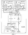
- FIG. 1is a schematic circuit diagram of an integrated circuit chip according to embodiments of the present invention.
- FIG. 2is a flow diagram of the operation of the circuit of FIG. 1 .
- FIG. 1is a schematic circuit diagram of an integrated circuit chip according to embodiments of the present invention.
- an integrated circuit chip 100includes two exemplary memory macros 105 A and 105 B.
- Memory macro 105 Aincludes a memory cell array 110 A comprising memory cells arranged in rows and columns, a repair register 115 A (which includes support and logic circuits) and a MUX 125 A.
- the rows and columns of memory cell array 110 Ainclude normal rows and columns and spare (or redundant) rows and columns. Generally rows are addressable as wordlines and columns as bitlines.
- a write bus 135 Ais connected to the I/O circuits of memory cell array 110 A, to repair register 115 A and to a first data input of MUX 125 A.
- the I/O circuits of memory cell array 110 A and a second data input of MUX 125 Aare connected by a read bus 140 A.
- Write buscarries both wordline and bitline addresses and column or bitline data, however only the column data is delivered to MUX 125 A (the branch of bus 135 A connected to MUX 125 A is a sub-bus).
- Read bus 140 Acarries only column or bitline data.
- Repair register 115 Ais connected to memory cell array 110 A by a bus 145 A to allow repair commands generated in the repair register to be transferred and implemented in memory cell array 110 A.
- Repair register 115 Ais connected to the switch input of MUX 125 A and can send a “HIT” signal 150 A which switches the output of MUX 125 A from read bus 140 A to write bus 135 A. This effectively redirects data on write bus 135 A back to the test circuits as described infra.
- Integrated circuit 100also includes an optional second memory macro 105 B, which is similar to memory macro 105 A.
- memory cell array 110 Bmay be the same array size (number of memory cells) or a different array size from memory cell array 110 A.
- Memory cell array 110 Bmay be the same array shape (number of rows and columns) or a different array shape as memory cell array 110 A.
- Memory cell array 110 Bmay be of the same type of memory or a different type of memory as memory cell array 110 A. Examples of types of memory include but are not limited to static random access memory (SRAM) and dynamic random access memory (DRAM).
- SRAMstatic random access memory
- DRAMdynamic random access memory
- Integrated circuit chip 100may include an optional error correction circuit (ECC) 155 .
- ECC 155When ECC 155 is included, the ECC unit includes a pass through function that is invoked in both operating modes (discussed infra) of the invention.
- Integrated circuit chip 100also includes a fail register 160 , an automatic built-in self-test (ABIST) macro 165 , a test/repair MUX 170 . a read MUX 175 and a write MUX 180 .
- ECC 155is connected to fail register 160 via a bus 185 .
- ABIST 165is connected to fail register 160 by a bus 190 and to a first data input of MUX 170 by a bus 195 .
- Fail register 160is connected to a second data input of MUX 170 by a bus 200 .
- the data output of MUX 170is connected to ECC 155 by a bus 205 .
- Buses 185 and 205are buses in the logic path connecting the memory macros to other circuits in integrated circuit 100 as opposed to being dedicated test buses. However test buses may be used.
- Buses 135 A and 135 Bare connected to respective data outputs of MUX 180 and buses 210 A and 210 B connect respective data outputs of MUXes 125 A and 125 B to data inputs of MUX 175 .
- the data output of MUX 175is connected to ECC 155 by a bus 210 and the data input of MUX 180 is connected to ECC 155 by a bus 215 .
- the switch inputs of MUXes 175 and 180are connected to ECC 155 by a bus 220 .
- the pass through function of ECC 155passes records/data on bus 205 to bus 215 unaltered and passes records/data on bus 210 to bus 185 unaltered.
- Test datais a pattern of bits that is written to the columns (bitlines) of memory arrays during test and resultant data is a pattern of bits read out of columns (bitlines) of the memory arrays after a period of test time.
- An expected patternis a pattern that will be read out of a memory array after writing a test pattern if the memory is working correctly.
- a repair recordincludes a memory macro ID field (if there are more than one memory macros), a type of fail field (wordline or bitline), a wordline address field and a data field as wide as the number of columns (bitlines, not counting redundant bitlines) in the memory array of the memory macro and indicating which bits failed. The data field indicates which bits are failing.
- ABIST 165generates a test pattern of bits that is sent to MUX 170 and presented to ECC 155 .
- ABISTalso sends an expected pattern of bits to fail register 160 .
- ECC 155sends a resultant pattern of bits to fail register 160 .
- Fail register 160generates fail record that is sent to MUX 170 and presented to ECC 155 .
- Fail registergenerates the fail record by comparing resultant patterns to expected patterns. Details of this process are described in U.S. Pat. No. 5,805,789 issued to Huott et al. on Sep. 8, 1998 and hereby incorporated by reference.
- the number of records that can be stored in fail register 160is half or less than the number of records that can be stored in repair register 115 A or repair register 115 B. Therefore an enhanced mode is provided, which is useful when the fail register 160 is significantly smaller than the repair registers 115 A and 115 B and the fail register must be cycled two or more times to complete testing of a memory cell array.
- repair registers 115 A and 115 Bsend a hit signal to respective MUXes 125 A and 125 B to redirect the entire test pattern to MUX 175 .
- the expected patternmust be the same as the test pattern. Since comparing a test pattern with itself will result in a passing test, fail register 160 will not generate another (redundant) repair record.
- fail register 160Since comparing a test pattern with itself will result in a passing test, fail register 160 will not generate another (redundant) repair record. Enhanced mode can be disabled or the circuits physically not present (in some or all of the memory macros) in an alternative embodiment of the present invention. For example, if the memory macro is small, then the repair register may be smaller than the fail register.
- FIG. 2is a flow diagram of the operation of the circuit of FIG. 1 .
- the methodstarts in step 290 .
- step 290if the testing is initializing then the method proceeds directly to step 300 otherwise it is determined if further testing is to be performed. If further testing is to be performed then the method proceeds to step 300 , otherwise the method proceeds to step 345 (via connector “A”).
- step 300ABIST sends a test pattern to a selected wordline of the memory macro.
- step 305ABIST sends an expected pattern to the fail register (in enhanced mode the expected pattern must be the same as the test pattern).
- step 310ABIST sends a read command to the memory macro.
- step 312which mode the test is being performed in is determined.
- step 315the memory macro sends a resultant pattern to the fail register.
- step 320the fail register compares the received and expected patterns and generates a data field of current fail record.
- step 325if a fail is detected (resultant and expected patterns don't match), the method proceeds to step 330 (unless all patterns have been used and testing is complete, in which case testing of the memory macro is complete) otherwise it loops back to step 300 for another test pattern.
- step 330it is determined if another fail record for the selected wordline already exists in the fail register. If another fail record for the current wordline does not exist the method proceeds to step 335 otherwise it loops back to step 300 for another test pattern (unless all patterns have been used and testing is complete, in which case testing of the memory macro is complete).
- step 335it is determined if the fail type should be changed from wordline to bitline. If the data field of the current fail record matches the data field of any other fail record in the fail register and the number of failing bits in the current fail record is less than a preset number of bits but at least equal to one, then the fail type field is changed from a wordline fail to a bitline fail and the fail record entered in the fail register.
- the present number of bitsmay range from 2 to the number of redundant bitlines available in the memory cell array. Generally, the present number will be small. In one example the present number is 1, 2 or 3. In one example, the present number is equal to about 10% of the number of redundant bitlines available. The method then proceeds to step 340 .
- step 340it is determined if the fail register is full. If the fail register is not full and an existing wordline fail was not changed to a bitline fail then a wordline fail record is created and the method loops back to step 300 . If the fail register is full the method proceeds to step 345 . In step 345 the fail register instructs ABIST to pause testing and send the fail records to the repair register and the method proceeds to step 350 .
- step 350the first/next fail record is received from the fail register and it is determined if the first (or next) fail record fail type field indicates a wordline or a bitline fail. If a wordline fail is indicated the method proceeds to step 360 otherwise to step 365 . In step 360 the repair register ignores the data field of the record, stores the fail record and issues a repair wordline command to the repair register. The method then proceeds to step 370 . In step 370 it is determined if another fail record is to be received from the fail register. If so, then the method loops back to step 350 , otherwise the method proceeds to step 375 .
- step 365the repair register ignores the wordline field of the record, stores repair record and issues a repair bitline command to the redundancy register.
- the methodthen proceeds to step 370 .
- step 370it is determined if another fail record is to be received from the fail register. If so, then the method loops back to step 350 , otherwise the method proceeds to step 375 .
- step 375it is determined if more testing of the memory macro is to be performed. If so, then the method loops back to step 300 , otherwise the method terminates or proceeds to testing another memory macro.
- Steps 385 through 400are performed only in enhanced mode.
- step 385up to three comparisons between the current fail record from fail register 160 (see FIG. 1 ) and the repair records of repair register 115 A/ 115 B are performed against three different sets of criteria in the following sequence. First, if the wordline address of the current test pattern matches any wordline address of any wordline repair record in said repair register then in step 390 the current test pattern to is returned to fail register 160 in step 320 .
- the expected pattern and said current test patternare the same pattern.
- a modified resultant patternis generated in repair register 115 A/ 115 B and returned to fail register 160 in step 320 .
- the modified resultant patternis generated by replacing the values of bits in positions of the resultant pattern corresponding to failing bit positions marked in the bitline repair record with the value of bits in the corresponding bit positions of the current test pattern.
- the resultant test patternis returned to fail register 160 in step 320 .
- Steps 300 through 400will repeat for each memory macro to be tested.
- the embodiments of the present inventionprovide a method and apparatus to reduce the area impact of test circuits of embedded memory macros without significant reduction in test coverage or increase in test time.
Landscapes
- For Increasing The Reliability Of Semiconductor Memories (AREA)
- Tests Of Electronic Circuits (AREA)
Abstract
Description
Claims (8)
Priority Applications (2)
| Application Number | Priority Date | Filing Date | Title |
|---|---|---|---|
| US11/612,628US7549098B2 (en) | 2006-12-19 | 2006-12-19 | Redundancy programming for a memory device |
| US12/046,508US7954028B2 (en) | 2006-12-19 | 2008-03-12 | Structure for redundancy programming of a memory device |
Applications Claiming Priority (1)
| Application Number | Priority Date | Filing Date | Title |
|---|---|---|---|
| US11/612,628US7549098B2 (en) | 2006-12-19 | 2006-12-19 | Redundancy programming for a memory device |
Related Child Applications (1)
| Application Number | Title | Priority Date | Filing Date |
|---|---|---|---|
| US12/046,508Continuation-In-PartUS7954028B2 (en) | 2006-12-19 | 2008-03-12 | Structure for redundancy programming of a memory device |
Publications (2)
| Publication Number | Publication Date |
|---|---|
| US20080148114A1 US20080148114A1 (en) | 2008-06-19 |
| US7549098B2true US7549098B2 (en) | 2009-06-16 |
Family
ID=39529081
Family Applications (1)
| Application Number | Title | Priority Date | Filing Date |
|---|---|---|---|
| US11/612,628Expired - Fee RelatedUS7549098B2 (en) | 2006-12-19 | 2006-12-19 | Redundancy programming for a memory device |
Country Status (1)
| Country | Link |
|---|---|
| US (1) | US7549098B2 (en) |
Cited By (2)
| Publication number | Priority date | Publication date | Assignee | Title |
|---|---|---|---|---|
| US20080282120A1 (en)* | 2007-05-11 | 2008-11-13 | Macronix International Co., Ltd. | Memory structure, repair system and method for testing the same |
| US9081060B2 (en) | 2013-10-04 | 2015-07-14 | Qualcomm Incorporated | Buffer testing for reconfigurable instruction cell arrays |
Families Citing this family (5)
| Publication number | Priority date | Publication date | Assignee | Title |
|---|---|---|---|---|
| US8495423B2 (en)* | 2009-08-11 | 2013-07-23 | International Business Machines Corporation | Flash-based memory system with robust backup and restart features and removable modules |
| US8117498B1 (en)* | 2010-07-27 | 2012-02-14 | Advanced Micro Devices, Inc. | Mechanism for maintaining cache soft repairs across power state transitions |
| KR101862379B1 (en) | 2013-04-19 | 2018-07-05 | 삼성전자주식회사 | Memory device with error correction code and redundancy repair operations |
| CN111863108A (en)* | 2019-04-29 | 2020-10-30 | 北京兆易创新科技股份有限公司 | Method and device for repairing storage unit in NOR flash memory |
| KR20240122176A (en)* | 2023-02-03 | 2024-08-12 | 삼성전자주식회사 | Memory repair circuit, memory repair method, and memory device |
Citations (12)
| Publication number | Priority date | Publication date | Assignee | Title |
|---|---|---|---|---|
| US5805789A (en) | 1995-12-14 | 1998-09-08 | International Business Machines Corporation | Programmable computer system element with built-in self test method and apparatus for repair during power-on |
| US5859804A (en) | 1991-10-16 | 1999-01-12 | International Business Machines Corporation | Method and apparatus for real time two dimensional redundancy allocation |
| US5920515A (en) | 1997-09-26 | 1999-07-06 | Advanced Micro Devices, Inc. | Register-based redundancy circuit and method for built-in self-repair in a semiconductor memory device |
| US6178126B1 (en) | 2000-03-23 | 2001-01-23 | International Business Machines Corporation | Memory and system configuration for programming a redundancy address in an electric system |
| US20020157051A1 (en) | 2001-04-24 | 2002-10-24 | International Business Machines Corporation | Method and apparatus for ABIST diagnostics |
| US6505317B1 (en)* | 2000-03-24 | 2003-01-07 | Sun Microsystems, Inc. | System and method for testing signal interconnections using built-in self test |
| US6574757B1 (en) | 2000-01-28 | 2003-06-03 | Samsung Electronics Co., Ltd. | Integrated circuit semiconductor device having built-in self-repair circuit for embedded memory and method for repairing the memory |
| US6934900B1 (en)* | 2001-06-25 | 2005-08-23 | Global Unichip Corporation | Test pattern generator for SRAM and DRAM |
| US7050343B2 (en) | 2003-02-27 | 2006-05-23 | Stmicroelectronics S.R.L. | Built-in testing methodology in flash memory |
| US7064990B1 (en) | 2005-02-09 | 2006-06-20 | International Business Machines Corporation | Method and apparatus for implementing multiple column redundancy for memory |
| US7089474B2 (en) | 2004-02-27 | 2006-08-08 | International Business Machines Corporation | Method and system for providing interactive testing of integrated circuits |
| US20080126901A1 (en)* | 2006-11-27 | 2008-05-29 | Taiwan Semiconductor Manufacturing Co., Ltd. | Memory with improved bist |
Family Cites Families (1)
| Publication number | Priority date | Publication date | Assignee | Title |
|---|---|---|---|---|
| US5707703A (en)* | 1994-03-10 | 1998-01-13 | Minnesota Mining And Manufacturing Company | Refastenable tube and cable restraint for medical use |
- 2006
- 2006-12-19USUS11/612,628patent/US7549098B2/ennot_activeExpired - Fee Related
Patent Citations (12)
| Publication number | Priority date | Publication date | Assignee | Title |
|---|---|---|---|---|
| US5859804A (en) | 1991-10-16 | 1999-01-12 | International Business Machines Corporation | Method and apparatus for real time two dimensional redundancy allocation |
| US5805789A (en) | 1995-12-14 | 1998-09-08 | International Business Machines Corporation | Programmable computer system element with built-in self test method and apparatus for repair during power-on |
| US5920515A (en) | 1997-09-26 | 1999-07-06 | Advanced Micro Devices, Inc. | Register-based redundancy circuit and method for built-in self-repair in a semiconductor memory device |
| US6574757B1 (en) | 2000-01-28 | 2003-06-03 | Samsung Electronics Co., Ltd. | Integrated circuit semiconductor device having built-in self-repair circuit for embedded memory and method for repairing the memory |
| US6178126B1 (en) | 2000-03-23 | 2001-01-23 | International Business Machines Corporation | Memory and system configuration for programming a redundancy address in an electric system |
| US6505317B1 (en)* | 2000-03-24 | 2003-01-07 | Sun Microsystems, Inc. | System and method for testing signal interconnections using built-in self test |
| US20020157051A1 (en) | 2001-04-24 | 2002-10-24 | International Business Machines Corporation | Method and apparatus for ABIST diagnostics |
| US6934900B1 (en)* | 2001-06-25 | 2005-08-23 | Global Unichip Corporation | Test pattern generator for SRAM and DRAM |
| US7050343B2 (en) | 2003-02-27 | 2006-05-23 | Stmicroelectronics S.R.L. | Built-in testing methodology in flash memory |
| US7089474B2 (en) | 2004-02-27 | 2006-08-08 | International Business Machines Corporation | Method and system for providing interactive testing of integrated circuits |
| US7064990B1 (en) | 2005-02-09 | 2006-06-20 | International Business Machines Corporation | Method and apparatus for implementing multiple column redundancy for memory |
| US20080126901A1 (en)* | 2006-11-27 | 2008-05-29 | Taiwan Semiconductor Manufacturing Co., Ltd. | Memory with improved bist |
Cited By (2)
| Publication number | Priority date | Publication date | Assignee | Title |
|---|---|---|---|---|
| US20080282120A1 (en)* | 2007-05-11 | 2008-11-13 | Macronix International Co., Ltd. | Memory structure, repair system and method for testing the same |
| US9081060B2 (en) | 2013-10-04 | 2015-07-14 | Qualcomm Incorporated | Buffer testing for reconfigurable instruction cell arrays |
Also Published As
| Publication number | Publication date |
|---|---|
| US20080148114A1 (en) | 2008-06-19 |
Similar Documents
| Publication | Publication Date | Title |
|---|---|---|
| US6667918B2 (en) | Self-repair of embedded memory arrays | |
| US5987632A (en) | Method of testing memory operations employing self-repair circuitry and permanently disabling memory locations | |
| KR102117633B1 (en) | Self repair device | |
| US5631868A (en) | Method and apparatus for testing redundant word and bit lines in a memory array | |
| US7284166B2 (en) | Programmable multi-mode built-in self-test and self-repair structure for embedded memory arrays | |
| US7490274B2 (en) | Method and apparatus for masking known fails during memory tests readouts | |
| US6259637B1 (en) | Method and apparatus for built-in self-repair of memory storage arrays | |
| US7474575B2 (en) | Apparatus for testing a memory of an integrated circuit | |
| US7549098B2 (en) | Redundancy programming for a memory device | |
| US20080022149A1 (en) | Enabling memory redundancy during testing | |
| KR101967270B1 (en) | Memory device and method for testing the same | |
| US7954028B2 (en) | Structure for redundancy programming of a memory device | |
| US6634003B1 (en) | Decoding circuit for memories with redundancy | |
| US6247153B1 (en) | Method and apparatus for testing semiconductor memory device having a plurality of memory banks | |
| US20060253723A1 (en) | Semiconductor memory and method of correcting errors for the same | |
| US6256243B1 (en) | Test circuit for testing a digital semiconductor circuit configuration | |
| US7518918B2 (en) | Method and apparatus for repairing embedded memory in an integrated circuit | |
| JP2005100542A (en) | Semiconductor memory device and test method thereof | |
| US7159156B2 (en) | Memory chip with test logic taking into consideration the address of a redundant word line and method for testing a memory chip | |
| KR20080010868A (en) | RAM testing and troubleshooting system | |
| JP4215723B2 (en) | Integrated circuit | |
| KR100959055B1 (en) | Internal memory device and system with integrated programmable self-test and its self-healing method | |
| US8458545B2 (en) | Method and apparatus for testing of a memory with redundancy elements | |
| US20070118778A1 (en) | Method and/or apparatus to detect and handle defects in a memory |
Legal Events
| Date | Code | Title | Description |
|---|---|---|---|
| AS | Assignment | Owner name:INTERNATIONAL BUSINESS MACHINES CORPORATION, NEW Y Free format text:ASSIGNMENT OF ASSIGNORS INTEREST;ASSIGNOR:BARTH, JOHN EDWARD, JR.;REEL/FRAME:018652/0144 Effective date:20061219 | |
| AS | Assignment | Owner name:INTERNATIONAL BUSINESS MACHINES CORPORATION, NEW Y Free format text:CORRECTIVE ASSIGNMENT TO ADD AN ASSIGNOR ON A DOCUMENT PREVIOUSLY RECORDED ON REEL 018652 FRAME 0144;ASSIGNORS:BARTH, JOHN EDWARD, JR.;GORMAN, KEVIN WILLIAM;REEL/FRAME:018751/0902 Effective date:20061219 | |
| FEPP | Fee payment procedure | Free format text:PAYOR NUMBER ASSIGNED (ORIGINAL EVENT CODE: ASPN); ENTITY STATUS OF PATENT OWNER: LARGE ENTITY | |
| REMI | Maintenance fee reminder mailed | ||
| LAPS | Lapse for failure to pay maintenance fees | ||
| STCH | Information on status: patent discontinuation | Free format text:PATENT EXPIRED DUE TO NONPAYMENT OF MAINTENANCE FEES UNDER 37 CFR 1.362 | |
| FP | Lapsed due to failure to pay maintenance fee | Effective date:20130616 | |
| AS | Assignment | Owner name:GLOBALFOUNDRIES U.S. 2 LLC, NEW YORK Free format text:ASSIGNMENT OF ASSIGNORS INTEREST;ASSIGNOR:INTERNATIONAL BUSINESS MACHINES CORPORATION;REEL/FRAME:036550/0001 Effective date:20150629 | |
| AS | Assignment | Owner name:GLOBALFOUNDRIES INC., CAYMAN ISLANDS Free format text:ASSIGNMENT OF ASSIGNORS INTEREST;ASSIGNORS:GLOBALFOUNDRIES U.S. 2 LLC;GLOBALFOUNDRIES U.S. INC.;REEL/FRAME:036779/0001 Effective date:20150910 |