US7549013B2 - Increasing the memory performance of flash memory devices by writing sectors simultaneously to multiple flash memory devices - Google Patents
Increasing the memory performance of flash memory devices by writing sectors simultaneously to multiple flash memory devicesDownload PDFInfo
- Publication number
- US7549013B2 US7549013B2US11/404,570US40457006AUS7549013B2US 7549013 B2US7549013 B2US 7549013B2US 40457006 AUS40457006 AUS 40457006AUS 7549013 B2US7549013 B2US 7549013B2
- Authority
- US
- United States
- Prior art keywords
- information
- sectors
- sector
- user data
- bytes
- Prior art date
- Legal status (The legal status is an assumption and is not a legal conclusion. Google has not performed a legal analysis and makes no representation as to the accuracy of the status listed.)
- Expired - Fee Related, expires
Links
Images


Classifications
- G—PHYSICS
- G06—COMPUTING OR CALCULATING; COUNTING
- G06F—ELECTRIC DIGITAL DATA PROCESSING
- G06F3/00—Input arrangements for transferring data to be processed into a form capable of being handled by the computer; Output arrangements for transferring data from processing unit to output unit, e.g. interface arrangements
- G06F3/06—Digital input from, or digital output to, record carriers, e.g. RAID, emulated record carriers or networked record carriers
- G06F3/0601—Interfaces specially adapted for storage systems
- G06F3/0602—Interfaces specially adapted for storage systems specifically adapted to achieve a particular effect
- G06F3/061—Improving I/O performance
- G06F3/0613—Improving I/O performance in relation to throughput
- G—PHYSICS
- G06—COMPUTING OR CALCULATING; COUNTING
- G06F—ELECTRIC DIGITAL DATA PROCESSING
- G06F12/00—Accessing, addressing or allocating within memory systems or architectures
- G06F12/02—Addressing or allocation; Relocation
- G06F12/0223—User address space allocation, e.g. contiguous or non contiguous base addressing
- G06F12/023—Free address space management
- G06F12/0238—Memory management in non-volatile memory, e.g. resistive RAM or ferroelectric memory
- G06F12/0246—Memory management in non-volatile memory, e.g. resistive RAM or ferroelectric memory in block erasable memory, e.g. flash memory
- G—PHYSICS
- G06—COMPUTING OR CALCULATING; COUNTING
- G06F—ELECTRIC DIGITAL DATA PROCESSING
- G06F3/00—Input arrangements for transferring data to be processed into a form capable of being handled by the computer; Output arrangements for transferring data from processing unit to output unit, e.g. interface arrangements
- G06F3/06—Digital input from, or digital output to, record carriers, e.g. RAID, emulated record carriers or networked record carriers
- G06F3/0601—Interfaces specially adapted for storage systems
- G06F3/0628—Interfaces specially adapted for storage systems making use of a particular technique
- G06F3/0638—Organizing or formatting or addressing of data
- G06F3/064—Management of blocks
- G—PHYSICS
- G06—COMPUTING OR CALCULATING; COUNTING
- G06F—ELECTRIC DIGITAL DATA PROCESSING
- G06F3/00—Input arrangements for transferring data to be processed into a form capable of being handled by the computer; Output arrangements for transferring data from processing unit to output unit, e.g. interface arrangements
- G06F3/06—Digital input from, or digital output to, record carriers, e.g. RAID, emulated record carriers or networked record carriers
- G06F3/0601—Interfaces specially adapted for storage systems
- G06F3/0668—Interfaces specially adapted for storage systems adopting a particular infrastructure
- G06F3/0671—In-line storage system
- G06F3/0673—Single storage device
- G06F3/0679—Non-volatile semiconductor memory device, e.g. flash memory, one time programmable memory [OTP]
- G—PHYSICS
- G11—INFORMATION STORAGE
- G11C—STATIC STORES
- G11C16/00—Erasable programmable read-only memories
- G11C16/02—Erasable programmable read-only memories electrically programmable
- G11C16/06—Auxiliary circuits, e.g. for writing into memory
- G11C16/08—Address circuits; Decoders; Word-line control circuits
- G—PHYSICS
- G11—INFORMATION STORAGE
- G11C—STATIC STORES
- G11C16/00—Erasable programmable read-only memories
- G11C16/02—Erasable programmable read-only memories electrically programmable
- G11C16/06—Auxiliary circuits, e.g. for writing into memory
- G11C16/10—Programming or data input circuits
- G11C16/102—External programming circuits, e.g. EPROM programmers; In-circuit programming or reprogramming; EPROM emulators
- G—PHYSICS
- G11—INFORMATION STORAGE
- G11C—STATIC STORES
- G11C29/00—Checking stores for correct operation ; Subsequent repair; Testing stores during standby or offline operation
- G11C29/70—Masking faults in memories by using spares or by reconfiguring
- G11C29/76—Masking faults in memories by using spares or by reconfiguring using address translation or modifications
- G11C29/765—Masking faults in memories by using spares or by reconfiguring using address translation or modifications in solid state disks
- G—PHYSICS
- G11—INFORMATION STORAGE
- G11C—STATIC STORES
- G11C29/00—Checking stores for correct operation ; Subsequent repair; Testing stores during standby or offline operation
- G11C29/70—Masking faults in memories by using spares or by reconfiguring
- G11C29/78—Masking faults in memories by using spares or by reconfiguring using programmable devices
- G11C29/80—Masking faults in memories by using spares or by reconfiguring using programmable devices with improved layout
- G11C29/816—Masking faults in memories by using spares or by reconfiguring using programmable devices with improved layout for an application-specific layout
- G11C29/82—Masking faults in memories by using spares or by reconfiguring using programmable devices with improved layout for an application-specific layout for EEPROMs
- G—PHYSICS
- G06—COMPUTING OR CALCULATING; COUNTING
- G06F—ELECTRIC DIGITAL DATA PROCESSING
- G06F11/00—Error detection; Error correction; Monitoring
- G06F11/07—Responding to the occurrence of a fault, e.g. fault tolerance
- G06F11/08—Error detection or correction by redundancy in data representation, e.g. by using checking codes
- G06F11/10—Adding special bits or symbols to the coded information, e.g. parity check, casting out 9's or 11's
- G06F11/1008—Adding special bits or symbols to the coded information, e.g. parity check, casting out 9's or 11's in individual solid state devices
- G06F11/1068—Adding special bits or symbols to the coded information, e.g. parity check, casting out 9's or 11's in individual solid state devices in sector programmable memories, e.g. flash disk
Definitions
- This inventionrelates to the field of digital systems, such as personal computers and digital cameras, employing nonvolatile memory as mass storage, for use in replacing hard disk storage or conventional film. More particularly, this invention relates to an architecture for increasing the performance of such digital systems by increasing the rate at which digital information is read from and written to the nonvolatile memory.
- nonvolatile memorysuch as flash or EEPROM memory
- flash or EEPROM memorymany digital systems have replaced conventional mass storage devices with flash and/or EEPROM memory devices.
- PCspersonal computers
- solid state storage devicesfor mass storage purposes in place of conventional hard disks.
- Digital camerasemploy solid state storage devices in cards to replace conventional films.
- FIG. 1shows a prior art memory system 10 including a controller 12 , which is generally a semiconductor (or integrated circuit) device, coupled to a host 14 which may be a PC or a digital camera.
- the controller 12is further coupled to a nonvolatile memory bank 16 .
- Host 14writes and reads information, organized in sectors, to and from memory bank 16 which includes a first nonvolatile memory chip 18 and a second nonvolatile memory chip 20 .
- Chip 18includes: an I/O register 22 having a port 24 connected to a port 26 of controller 12 via a first bus 28 which includes 8 bit lines; and a storage area 30 coupled with I/O register 22 .
- Chip 20includes: an I/O register 32 having a port 34 connected to a port 36 of controller 12 via a second bus 38 which includes 8 bit lines; and a storage area 40 coupled with I/O register 32 .
- the first and second buses 28 , 38are used to transmit data, address, and command signals between the controller and the memory chips 18 and 20 .
- the least significant 8 bits (LSBs) of 16 bits of informationare provided to chip 18 via the first bus 28
- MSBsmost significant 8 bits
- Memory bank 16includes a plurality of block locations 42 each of which includes a plurality of memory row locations.
- Each block location of the memory bankis comprised of a first sub-block 44 located in the first non-volatile memory chip, and a corresponding second sub-block 46 located in the second non-volatile memory chip.
- Each memory row locationincludes a first row-portion 48 and a corresponding second row-portion 50 .
- each of the first and second row-portions 48 and 50includes storage for 256 bytes of data information plus an additional 8 bytes of storage space for overhead information.
- a sectorincludes 512 bytes of user data and 16 bytes of non-user data (the latter commonly referred to as overhead information)
- 256 bytes of the user data and 8 bytes of the overhead information of the sectormay be maintained in the first row portion 48 of chip 18 and the remaining 256 bytes of user data and remaining 8 bytes of overhead information of the same sector may be maintained in the second row portion 50 of chip 20 .
- half of a sectoris stored in a memory row location 48 of chip 18 and the other half of the sector is stored in memory row location 50 of chip 20 .
- half of the overhead information of each stored sectoris maintained by chip 18 and the other half by chip 20 .
- reading and writing data to flash memory chips 18 and 20is time consuming.
- Writing data to the flash memory chipsis particularly time consuming because data must be latched in I/O registers 22 and 32 , which are loaded 1 byte at a time via the first and second buses, and then transferred from the I/O registers 22 and 32 to the memory cells of the flash memory chips 18 and 20 respectively.
- the time required to transfer data from the I/O registers to memory, per byte of data,is proportional to the size of the I/O registers and the size of the flash memory chip.
- controller 12writes a single sector of information to memory bank 16 by: (1) transmitting a write command signal to each of chips 18 and 20 via buses 28 and 38 simultaneously; (2) transmitting address data to chips 18 and 20 specifying corresponding sub-blocks 44 and 46 of the chips via buses 28 and 38 simultaneously; and (3) sequentially transmitting a byte of user data to each of chips 18 and 20 via buses 28 and 38 simultaneously for storage in the corresponding sub-blocks 44 and 46 .
- the problem with such prior art systemsis that while two bytes of information are written and read at a time, only one sector of information is accommodated at a time by the memory bank 16 during a write command initiated by the host 14 .
- FIG. 2Another prior art digital system 60 is shown in FIG. 2 to include a controller 62 coupled to a host 64 , and a nonvolatile memory bank 66 for storing and reading information organized in sectors to and from nonvolatile memory chip 68 , included in the memory bank 66 . While not shown, more chips may be included in the memory bank, although the controller, upon command by the host, stores an entire sector in one chip.
- a blocksuch as block 0 , includes 16 sectors S 0 , S 1 , . . . , S 15 .
- an I/O register 70Also included in the chip 68 is included in the chip 68 , which includes 512 bytes plus 16 bytes, a total of 528 bytes, of storage space.
- the controllertransfers information between host 64 and memory 66 a byte at-a-time.
- a sector of 512 bytes of user data plus 16 bytes of overhead informationis temporarily stored in the I/O register during a write operation and then transferred to one of the blocks within the memory device for storage thereof.
- a sector of informationis read from one of the blocks of the memory device and then stored in the I/O register for transfer to the controller.
- An important problem with the prior art architecture of FIG. 2is that while a total of 528 bytes may be stored in the I/O register 36 , only one byte of sector information may be transferred at a time between the controller and the memory bank thereby impeding the overall performance of the system.
- LBA to PBA mapping informationfor translating a host-provided logical block address (LBA) identifying a sector of information to a physical block address (PBA) identifying the location of a sector within the memory bank.
- LBAhost-provided logical block address
- PBAphysical block address
- This mapping informationmay generally be included in volatile memory, such as a RAM, within the controller, although it may be maintained outside of the controller.
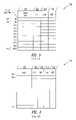
- FIG. 3shows a table diagram illustrating an example of an LBA-PBA map 300 defined by rows and columns, with each row 302 being uniquely identified, addressed, by a value equal to that of the LBA received from the host divided by 16.
- the row numbers of FIG. 3are shown using hexadecimal notation. Thus, for example, row 10H (in Hex.) has an address value equal to 16 in decimal.
- Each row 302 of map 300includes a storage location field 304 for maintaining a virtual PBA value, an ‘old’ flag field 306 , a ‘used’ flag field 308 , and a ‘defect’ flag field 310 .
- the flag fieldsprovide information relating to the status of a block of information maintained within the memory bank (in FIGS. 1 and 2 ).
- the virtual PBA field 304stores information regarding the location of the block within the memory bank.
- FIG. 4shows a table diagram illustrating an exemplary format for storage of a sector of data maintained in a memory bank.
- the virtual PBA field 304( FIG. 3 ) provides information regarding the location of a block 400 of information with each block having a plurality of sectors 402 .
- Each sector 402is comprised of a user data field 404 , an ECC field 406 , an ‘old’ flag field 408 , a ‘used’ flag field 410 and a ‘defect’ flag field 412 .
- table 300occupies much ‘real estate’ and since it is commonly comprised of RAM technology, which is in itself costly and generally kept within the controller, there is substantial costs associated with its manufacturing. Furthermore, as each row of table 300 is associated with one block of information, the larger the number of blocks of information, the larger the size of the table, which is yet an additional cost for manufacturing the controller and therefore the digital system employing such a table.
- the present inventionincludes a digital system having a controller semiconductor device coupled to a host and a nonvolatile memory bank including a plurality of nonvolatile memory devices.
- the controllertransfers information, organized in sectors, with each sector including a user data portion and an overhead portion, between the host and the nonvolatile memory bank and stores and reads two bytes of information relating to the same sector simultaneously within two nonvolatile memory devices.
- Each nonvolatile memory deviceis defined by a row of memory locations wherein corresponding rows of at least two semiconductor devices maintain two sectors of information therein with the overhead information relating to the two sectors maintained in one of the memory rows of the nonvolatile memory device.
- Each 32 sectors of informationdefines a block identified by a virtual physical block address with a block of information expanding between two memory devices wherein an even and an odd byte of a sector is simultaneously read from or written to two nonvolatile memory devices.
- the controllerstores an entire sector of information within a single nonvolatile memory device and reads from or writes to, a sector of information by processing corresponding bytes of at least two sectors in two nonvolatile memory devices simultaneously.
- FIG. 1is a block diagram of a prior art memory system in which a single sector of information is written, two bytes at a time during a write operation, to a memory bank including two memory units each having capacity to store 256 bytes of user data in a single row location.
- FIG. 2is a block diagram of a prior art memory system in which a single sector of information is written, one byte at a time during a write operation, to a memory bank including at least one memory unit having capacity to store 512 bytes of user data in a single row location.
- FIG. 3is a table diagram illustrating an exemplary map for translating a host-provided logical block address (LBA) identifying a sector of information to a physical block address (PBA) identifying a location for the sector within a memory bank.
- LBAhost-provided logical block address
- PBAphysical block address
- FIG. 4is a table diagram illustrating an exemplary format for storage of a sector of data maintained in a memory bank.
- FIG. 5is a generalized block diagram of a memory system in accordance with the present invention in which two sectors of information are written, two bytes at a time during a single write operation, to a memory bank including at least two memory units each having capacity to store 512 bytes of user data in a single row location.
- FIG. 6is a detailed block diagram of the memory system of FIG. 5 .
- FIG. 7is a table diagram generally illustrating a memory storage format for storing a block, including 32 sectors, of information in a memory bank including two non-volatile memory units wherein an even sector and an odd sector are stored in a single memory row location and wherein even data bytes of both sectors are stored in a row portion located in a first of the memory units and odd data bytes of both sectors are stored in a second row portion located in the second of the memory units.
- FIG. 8Ais a table diagram generally illustrating organization of an exemplary LBA-PBA map for use in accordance with the present invention.
- FIG. 8Bshows a block diagram illustrating formats of address information identifying sectors and associated blocks of information in accordance with the present invention.
- FIG. 9is a timing diagram illustrating the timing of control, address, and data signals for a write operation performed by the memory system of FIG. 6 wherein two sectors of information are simultaneously written, during a single write operation, to a memory bank having the memory storage format illustrated in FIG. 7 .
- FIG. 10is a table diagram illustrating a memory bank having a memory storage format as depicted in FIG. 7 wherein a single sector is written to a particular memory row location of the memory bank.
- FIG. 11is a table diagram illustrating a memory bank having an alternative memory storage format as depicted in FIG. 7 wherein a single sector is written to a particular memory row location of the memory bank.
- FIGS. 12 , 12 - 1 and 12 - 2are flowcharts illustrating a process of simultaneously writing two sectors of information to two memory units during a single write operation in accordance with the present invention.
- FIG. 12 ashows a flow chart of the steps performed in executing the defect management routine of FIG. 12 .
- FIG. 13is a table diagram generally illustrating an alternative memory storage format for storing a block, including 32 sectors, of information in a memory bank including two non-volatile memory units wherein an even sector and an odd sector are stored in a single memory row location and wherein an even sector is stored in a first row portion located in a first of the two memory units and an odd sector is stored in a second row portion located in the second of the two memory units.
- FIG. 14shows a timing diagram illustrating the timing of control, address, and data signals for a process of erasing a block of a memory bank in accordance with principles of the present invention.
- FIG. 15is a flowchart illustrating a process of erasing a block, including a first sub-block stored in a first memory unit and a second sub-block stored in a second memory unit, in accordance with the present invention.
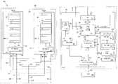
- FIG. 5shows a generalized block diagram at 500 of a memory system in accordance with principles of the present invention.
- the systemincludes a memory card 502 coupled to a host system 504 .
- host 504is a digital camera and memory card 502 is a digital film card
- host 504is a personal computer system and memory card 502 is a PCMCIA card.
- Memory card 502includes: a non-volatile memory bank 506 including a plurality of non-volatile memory units 508 for storing sectors of information organized in blocks; a memory controller 510 coupled to the memory bank via a memory bus 512 , and coupled to the host 504 via a host bus 514 .
- Memory controller 510controls transfer of sector-organized information between host 504 and memory bank 506 . Each sector of information includes a user data portion and an overhead portion. The memory controller performs write and read operations, in accordance with the present invention, to and from the memory units of the memory bank as further explained below.
- the non-volatile memory bank 506may include any number of non-volatile memory units 508 while in a preferred embodiment, the non-volatile memory bank has an even number of memory units. Also in the preferred embodiment, each of the non-volatile memory units is a flash memory integrated circuit device.
- FIG. 6shows a detailed block diagram at 600 of the memory system of FIG. 5 .
- Controller 510is shown to include: a host interface 610 connected to the host 504 via host bus 514 for transmitting address, data, and control signals between the controller and the host; a data buffer 614 having a port 616 coupled to a port 618 of the host interface; a microprocessor 620 having a port 622 coupled to a port 624 of the host interface; a code storage unit 626 having a port 628 coupled to a port 630 of the microprocessor; a boot ROM unit 632 having a port 634 coupled to port 630 of the microprocessor and to port 628 of the code storage unit; a space manager 636 having a port 638 coupled to a port 640 of the microprocessor; a flash state machine 642 including a port 644 coupled to a port 646 of the microprocessor, a port 648 coupled to a port 650 of the space manager, and a port 645 coupled to a port
- memory bank 506includes two non-volatile memory units (although additional memory units may be included, only two are shown for simplicity); a first flash memory chip 670 designated FLASH 0 and a second flash memory chip 672 designated FLASH 1 .
- First flash memory chip 670includes a first input/output register (first I/O register) 671 and a storage area 669 .
- Second flash memory chip 672includes a second input/output register (second I/O register) 673 and a storage area 674 .
- Memory bus 512is used to transmit address, data, and control signals between the controller 510 and memory bank 506 .
- Memory bus 512includes a flash bus 675 connected to a port 676 of memory I/O unit 652 for transmitting address, data, and command signals between flash memory chips 670 , 672 and the memory I/O unit 652 .
- Flash bus 675includes 16 bit lines, 8 bit lines of which form a first bus 680 connected to a port 682 of I/O register 671 of the first flash memory chip, and another 8 bit lines of which form a second bus 684 connected to a port 686 of I/O register 673 of the second flash memory chip.
- Memory bus 512also includes: a control bus 690 which connects a control signal (CTRL signal) output 692 of the flash state machine 642 to an input 694 of the first flash memory chip and to an input 696 of the second flash memory chip; a chip enable line 698 which connects a chip enable (CE) output 700 of the flash state machine 642 to an enable input 702 of the first flash memory chip and to enable an input 704 of the second flash memory chip; and a ready/busy signal (FRDY-BSY* signal) line 706 which connects an output 708 of the first flash memory chip and an output 710 of the second flash memory chip to an input 712 of the flash state machine 642 .
- CTRL signalcontrol signal
- CEchip enable
- FRDY-BSY* signalready/busy signal
- Microprocessor 620executes program instructions (or code) stored in ROM 632 , and at other times, such as during operation of the memory system, the microprocessor executes code that is stored in code storage unit 626 , which may be either a volatile, i.e., read-and-write memory (RAM) or a non-volatile, i.e., EEPROM, type of memory storage. Prior to the execution of program code from code storage unit 626 , the program code may be stored in the memory bank 506 and later downloaded to the code storage unit for execution thereof. During initialization, the microprocessor 620 can execute instructions from ROM 632 .
- Sector-organized informationincluding user data and overhead information, is received at host interface 610 from host 504 via host bus 514 and provided to the data buffer 614 for temporary storage therein. Sectors of information stored in the data buffer are retrieved under control of flash state machine 642 and provided to memory bank 506 in a manner further described below. It is common in the industry for each sector to include 512 bytes of user data plus overhead information. Although a sector may include other numbers of bytes of information, in the preferred embodiment, a sector has 512 bytes of user data and 16 bytes of overhead information.
- ECC logic block 660includes circuitry for performing error coding and correction on the sector-organized information. ECC logic block 660 performs error detection and/or correction operations on the user data portions of each sector stored in the flash memory chips 670 , 672 or data received from host 504 .
- the space manager 636finds a next unused (or free) non-volatile memory location within the memory bank for storing a block of information with each block including multiple sectors of information.
- a blockincludes 32 sectors although, alternatively a block may be defined to include another number of sectors such as, for example, 16.
- the physical address of a storage block located within memory bank 506referred to as a virtual physical block address (virtual PBA)
- the physical block address of a sector of information located within the memory bank 506referred to as an actual physical block address (actual PBA)
- LBAlogical block address
- Space manager 636includes a space manager memory unit, which is preferably a volatile memory unit, for storing an LBA-PBA map for translating a modified version of the host-provided LBAs to virtual PBAs as further explained below.
- the space managerincludes a space manager RAM unit (SPM RAM unit) 720 for storing the LBA-PBA map under the control of a space manager controller (SPM controller) 724 which is coupled to the SPM RAM unit.
- SPM RAM unitspace manager RAM unit
- SPM controllerspace manager controller
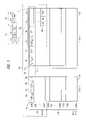
- FIG. 7shows a table diagram generally illustrating organization of user data, error correction information, and flag information stored in memory bank 506 in accordance with an embodiment of the present invention.
- Memory bank 506includes a plurality of M blocks 727 designated BLCK 0 , BLCK 1 , BLCK(M ⁇ 1), each having a virtual physical block addresses (PBA).
- Each block 727 of memory bank 506is comprised of a first sub-block 730 of first flash memory chip 670 , and a corresponding second sub-block 731 of second flash memory chip 672 .
- Corresponding sub-blocks 730 , 731which together form a block, are identified by the same virtual PBA.
- Each memory row location 728includes a first row-portion 732 and a corresponding second row-portion 733
- each of the first and second row-portions 732 , 733includes storage for 512 bytes of data information plus additional storage space for other information.
- the storage of information in the first row-portions 732 of the first flash memory chipis accomplished in a manner dissimilar from that in the second row-portions 733 of the second flash memory chip.
- Each of the first row-portions 732includes: a first even sector field 734 for storing even data bytes D 0 , D 2 , D 4 , . . . D 510 of an even sector (S 0 , S 2 , S 4 , . . . ) of information; a first spare field 736 ; a first odd sector field 738 for storing even data bytes D 0 , D 2 , D 4 , . . . D 510 of an odd sector (S 1 , S 3 , S 5 , . . . ) of data; and a second spare field 740 .
- Each of the second row-portions 733includes: a second even sector field 742 for storing odd data bytes D 1 , D 3 , D 5 , . . . D 511 of the even sector of data which has it's corresponding even data bytes stored in first even sector field 734 ; a first error correction field 744 for storing error correction information corresponding to the even sector of information stored collectively in fields 734 and 742 ; a second odd sector field 746 for storing odd data bytes of the odd sector of information which has it's even data bytes stored in first odd sector field 738 ; a second error correction field 748 for storing ECC information corresponding to the odd sector of information stored collectively in fields 738 and 746 ; a block address field 750 ; and a flag field 752 .
- Fields 734 and 742form an even sector location while fields 738 and 746 form an odd sector location. It is understood in the present invention that fields 734 and 742 could alternatively form an odd sector location while fields 738 and 746 could alternatively form an even sector location, and that fields 734 and 738 could alternatively be used to store odd data bytes while fields 742 and 746 could alternatively be used to store even data bytes. Additionally, first row-portion 732 could alternatively be used for storing the overhead information relating to the sectors stored in the memory row location 728 .
- Flag field 752is used for storing flag information which is used by controller 510 ( FIG. 6 ) during access operations as further explained below.
- Block address field 750is used for storing a modified version of a host-provided LBA value which is assigned to a block, as further described below. Only a single block address entry is required in the block address field per block.
- a modified host-provided LBA valueis entered in block address field 759 of the Nth row, ROW 15 , of the row locations 728 of each block 727 .
- the controller 510accesses an even sector of information stored collectively in the first and second flash memory chips by simultaneously accessing first and second even sector fields 734 , 742 of corresponding row-portions of the first and second flash memory chips via the first and second split buses 680 , 684 ( FIG. 6 ), respectively.
- the first and second split buses 680 , 684include lines coupled to receive the even and odd data bytes respectively of a sector of information.
- the controller 510 ( FIG. 6 )accesses an odd sector of information stored collectively in the first and second flash memory chips by simultaneously accessing the first and second odd sector fields 738 , 746 via the first and second split buses 680 , 684 ( FIG. 6 ), respectively.
- the split buses 680 , 684( FIG. 6 ) also provide for: transmission of ECC information between the flash memory chips and the flash state machine 642 and ECC logic unit 660 of the memory controller 510 ; and transmission of address information from flash state machine 642 to the flash memory chips.
- Controller 510monitors the status of blocks 727 of memory bank 506 using the space manager 636 .
- controller 510monitors the status of each block location 727 of the memory bank using block level flags including a used/free block flag and a defect block flag stored in a used flag location 754 and a defect flag location 756 respectively of the flag field 752 .
- Block level flagsprovide information concerning the status of a whole block 727 of the memory bank and therefore, only a single block level flag entry is required in the flag locations 754 and 756 per block.
- the used/new block flagindicates whether the corresponding block 727 is currently being “used” to store information or whether it is available (or free) to store information.
- the defect block flagindicates whether the corresponding block 727 is defective.
- controller 510monitors the status of each memory row location 728 of the memory bank using flags including a used/free row flag stored in the used flag location 754 , a defect row flag stored in the defect flag location 756 , an old row flag stored in an old flag location 758 of the flag field 752 , an even sector move flag stored in an even sector move flag location 760 , and an odd sector move flag stored in an odd sector move flag location 762 .
- the used/new flagindicates whether the corresponding memory row location 728 is currently being “used” to store information or whether it is available (or free) to store information.
- the defect flagindicates whether the memory block 727 is defective.
- locations 758 , 754 , and 756are included in a single 3-bit flag location 764 .
- the even and odd sector move flag locations 760 , 762store values indicating whether the corresponding even and odd sectors stored in the non-volatile memory sector location have been moved to another location within the non-volatile memory bank 506 ( FIG. 6 ). For example, if an even sector of information stored collectively in a particular pair of even sector fields 734 , 742 of a row location 728 has been moved to another pair of even sector fields in the non-volatile memory bank 506 , the value in the corresponding even sector move flag location 760 is set.
- locations 760 and 762are formed by a single 2-bit move-flag location 766 .
- FIG. 8Ashows a table diagram generally illustrating organization of an exemplary LBA-PBA map at 800 , which is stored in SPM RAM 720 ( FIG. 6 ), for translating a modified version of the host-provided LBA's to PBA's.
- the modified host-provided LBAis derived by dividing the host-provided LBA by the number of sectors with a block, as explained in more detail below.
- the depicted LBA-PBA mapincludes: a plurality of map row locations 802 which are addressable by a modified host-provided LBA or by a virtual PBA; a virtual PBA field 804 for storing a virtual PBA value identifying a block 727 ( FIG.
- the actual PBAspecifies the location of a sector of information in the memory bank and the virtual PBA specifies the location of a block 727 ( FIG. 7 ) in the memory bank.
- Virtual PBA valuesare retrieved by space manager 636 ( FIG. 7 ) from the depicted map and transferred to port 648 of the flash state machine 642 for use in addressing blocks within memory bank 506 .
- FIG. 8Bshows a block diagram illustrating a host-provided-LBA format 810 and an actual PBA format 820 .
- LBA format 810includes “offset bits” 812 , which comprise the least significant bits of the host-provided LBA value.
- each block 727( FIG. 7 ) includes memory space for storing 32 sectors of information, each sector includes 512 bytes of user data and 16 bytes of overhead information. Because each block 727 ( FIG. 7 ) includes 32 sectors in the preferred embodiment, five offset bits 812 are required to identify each of the 32 sectors in each block.
- the translation of the host-provided-LBA to actual and virtual PBA valuesis performed by first masking the five least significant “offset” bits 812 , of the host-provided-LBA, shifting the result to the right by 5 bits and using the shifted value as a modified host-provided LBA value or an “LBA-map-value” to address a map row location 802 in the LBA-PBA map 800 ( FIG. 8A ). This, in effect, is dividing the host-provided LBA by 32.
- the actual PBA value 820which specifies the location of a sector within a block of the memory bank, is formed by concatenating offset bits 812 of the LBA value with a virtual PBA 822 value stored in the corresponding field 804 ( FIG. 8A ) of the LBA-PBA map. That is, the virtual PBA value 822 is used to identify a block within the memory bank and the five remaining offset bits 812 are used to address a sector within the identified block.
- the virtual PBA value stored in the virtual PBA field 804 of each map row location 802is set to an all ‘1’s state.
- the virtual PBA value stored in the corresponding virtual PBA field 804 of the corresponding map row locationis modified by the space manager controller 724 ( FIG. 6 ) to specify a new virtual PBA value.
- the old virtual PBA value(the virtual PBA value corresponding to the erased block), rather than a modified version of the host-provided LBA, is used to address the SPM RAM 720 ( FIG.
- FIG. 9shows a timing diagram illustrating the timing of control, address, and data signals for a write operation performed by memory system 600 ( FIG. 6 ) wherein two sectors of information are simultaneously written in the non-volatile memory bank 506 ( FIG. 6 ) during a single write operation.
- the diagramincludes: a wave form 902 representing a first flash signal which transmits time multiplexed command, address, and data information from flash state machine 642 ( FIG. 6 ) of the controller via bus 680 ( FIG. 6 ) to port 682 of the first flash memory chip; a wave form 904 representing a second flash signal which transmits time multiplexed command, address, and data signals from the flash state machine via bus 684 ( FIG. 6 ) to port 686 of the second flash memory chip; a time line 905 ; and a plurality of control signal wave forms.
- the control signal wave formsinclude: a wave form 906 representing a command line enable signal (CLE signal) transmitted from flash state machine 642 ( FIG. 6 ) to the first and second flash memory chips via control bus 690 ( FIG. 6 ); a wave form 908 representing an address line enable signal (ALE signal) transmitted from the flash state machine to the flash memory chips via the control bus; a wave form 910 representing a write enable signal (WE signal) transmitted from the flash state machine to the flash memory chips via the control bus; a wave form 912 representing a read enable signal (RE signal) transmitted from the flash state machine to the memory chips via the control bus; a wave form 914 representing a flash chip enable signal (FCE* signal) transmitted from chip enable signal output 700 ( FIG.
- CLE signalcommand line enable signal
- ALE signaladdress line enable signal
- WE signalwrite enable signal
- RE signalread enable signal
- FCE* signalflash chip enable signal
- a wave form 916 representing a flash ready/busy signal(FRDY_BSY* signal) transmitted from outputs 708 and 710 ( FIG. 6 ) of the first and second flash memory chips to the flash state machine via flash ready/busy signal line 706 .
- the write operationcommences at a time to at which the FCE* signal (wave form 914 ) transitions from a HIGH state to a LOW state thereby enabling the first and second flash memory chips to begin receiving command, address, data, and control signals.
- the FRDY_BSY* signal(wave form 916 ), transmitted from the flash memory chips to input 712 of the flash state machine ( FIG. 6 ), is already activated indicating that the first and second flash memory chips are ready to receive access commands.
- the CLE signal(wave form 906 ) is activated, transitioning from a LOW state to a HIGH state, thereby enabling the first and second flash memory chips to read command signals.
- the first and second flash signals(wave forms 902 and 904 ) simultaneously transmit a serial data shift-in command signal 80 H to the first and second flash memory chips via the first and second first split buses 680 and 684 respectively.
- the WE signal(wave form 910 ) transitions from a HIGH state to a LOW state thereby enabling the first and second flash memory chips to read the serial data command signals 80 H.
- the CLE signal(wave form 906 ) is deactivated, transitioning back to the LOW state, thereby disabling the flash memory chips from reading command signals.
- the ALE signal(wave form 908 ) is activated, transitioning from a LOW state to a HIGH state, thereby enabling the first and second flash memory chips to read packets of address information.
- the first and second flash signals(wave forms 902 and 904 ) each transmit first, second, and third address packets ADD 0 , ADD 1 , and ADD 2 respectively to the first and second flash memory chips.
- the ALE signal(wave form 908 ) is deactivated, transitioning from the HIGH state to a LOW state, thereby disabling the first and second flash memory chips from reading address information.
- the WE signaltransitions from a HIGH state to a LOW state thereby enabling the first and second flash memory chips to read the read the first, second, and third address packets ADD 0 , ADD 1 , and ADD 2 respectively.
- the three address packets ADD 0 , ADD 1 , and ADD 2specify a row-portion 732 , 733 within a first sub-block 730 ( FIG. 16 ).
- the first and second flash signalsbegin simultaneously transmitting interleaved even and odd data bytes wherein the even and odd bytes form one sector of information.
- the even bytesare transmitted to the first flash memory chip via bus 680 ( FIG. 6 ) and the odd sector bytes are transmitted to the second flash memory chip via bus 684 ( FIG. 6 ).
- the even data bytes D 0 , D 2 , D 4 , . . . D 510 of the even sectorare received by the first flash chip and stored in the first even sector field 734 ( FIG. 16 ) of the corresponding location 732 of the first flash memory chip.
- the write enable signal WE*(Wave form 910 ) is activated.
- the odd data bytes D 1 , D 3 , D 5 , . . . D 511 of the even sectorare received by the second flash chip and stored in the second even sector field 742 ( FIG. 16 ) of the corresponding location 733 thereof with each byte being stored when the WE* signal is activated.
- the first and second flash signals(wave forms 902 and 904 ) complete transmission of the interleaved even and odd data bytes of the even sector:
- the first flash signal(wave form 902 ) transmits four packets of filler information (FFH, hexadecimal F, equivalent binary value “1111,” decimal value “15”) to the first flash memory chip via the first split bus 680 ( FIG. 6 ) while the second flash signal (wave form 904 ) transmits error correction codes (ECC) to the second flash memory chip via the second split bus 684 ( FIG. 6 ).
- the filler information FFH transmitted during this time periodis received by the first flash memory chip and stored in the first spare field 736 ( FIG. 16 ).
- the error correction code transmitted during this time periodis received by the second flash memory chip and stored in the first error correction field 744 ( FIG. 16 ) of the nonvolatile memory section 733 of the second flash memory chip.
- This error correction codegenerated by ECC logic unit 660 ( FIG. 16 ), relates to the even sector transmitted during the preceding time interval between time t 10 and t 11 .
- the first and second flash signalsbegin simultaneously transmitting interleaved even and odd data bytes, synchronous with the write enable signal WE* (wave form 910 ), of an odd sector to the first and second flash memory chips via the first and second first split buses 680 and 684 ( FIG. 6 ) respectively.
- the even data bytes D 0 , D 2 , D 4 , . . . D 510 of the odd sectorare received by the first flash chip and stored to the first odd sector field 738 ( FIG. 16 ) of the corresponding location 732 of the first flash memory chip.
- the D 511 of the odd sectorare received by the second flash memory chip and stored to the second odd sector field 746 ( FIG. 16 ) of the corresponding location 733 of the second flash memory chip.
- the first and second flash signals(wave forms 902 and 904 ) complete transmission of the interleaved even and odd data bytes of the odd sector.
- the first flash signal(wave form 902 ) transmits no information to the first flash memory chip thereby maintaining the value in corresponding storage location bytes of the first flash memory chip at FFH (hexadecimal) or all 1's in binary.
- the second flash signal(wave form 904 ) transmits error correction codes (ECC) to the second flash memory chip via the second split bus 684 ( FIG. 6 ).
- ECCerror correction codes
- the error correction code transmitted during this time periodis received by the second flash memory chip and stored to the second error correction field 748 ( FIG. 16 ) of the nonvolatile memory section 733 of the second flash memory chip.
- This error correction codegenerated by ECC logic unit 660 ( FIG. 16 ), relates to the odd sector transmitted during the preceding time interval between time t 11 and t 12 .
- the first and second flash signalseach transmit a read command signal 70 H to the first and second first and second flash memory chips via the first and second split buses 680 and 684 respectively.
- the WE signaltransitions from a HIGH state to a LOW state thereby enabling the first and second flash memory chips to read the read command signals 70 H.
- the CLE signal(wave form 906 ) is deactivated, transitioning back to the LOW state, thereby disabling the flash memory chips from reading command signals.
- the first and second flash signals(wave forms 902 and 904 ) each transmit a status command signal STATUS to the first and second first and second flash memory chips via the first and second split buses 680 and 684 respectively.
- the WE signal(wave form 910 ) transitions from a HIGH state to a LOW state thereby enabling the first and second flash memory chips to read the read command signals 70 H.
- FIG. 10shows a table diagram generally illustrating the memory storage format, as depicted in FIG. 7 , for storing a block of information in memory bank 506 ( FIG. 6 ) wherein a single sector is written to a particular memory row location of the memory bank.
- a memory row location 728 designated ROW 1has an even sector S 2 and an odd sector S 3 stored therein in accordance with the format described above in reference to FIG. 7 .
- a memory row location 728 designated ROW 2has a single even sector S 4 stored in the first and second even sector fields 734 and 742 of a corresponding pair of row-portions of the first and second flash memory chips 670 , 672 . Because no odd sector is required to be stored in this case, fields 736 , 738 , 746 , 748 , 750 , and 752 are shown to be erased.
- FIG. 11shows a table diagram illustrating the alternative memory storage format, as depicted in FIG. 7 , for storing a block of information in memory bank 506 ( FIG. 6 ) wherein a single sector is written to a particular memory row location of the memory bank.
- field 764is a three bit field which is used for storing the old row flag in the first bit place, the used/free row flag in the second bit place, and the defect row flag in the third bit place.
- field 766is a two bit field which is used for storing the even sector move flag in the first bit place and the odd sector move flag in the second bit place.
- the memory row location designated ROW 1having sectors S 2 and S 4 stored therein, has a value “00” stored in field 766 indicating that both sectors have been moved elsewhere in the memory bank.
- the memory row location designated ROW 2having a single even sector S 4 stored in the first and second even sector fields 734 and 742 , has a value “01” stored in field 766 indicating that the information in S 4 has been updated and now resides elsewhere in the memory bank.
- a value of logic state “0”generally indicates that moved sectors have been updated by the host. Therefore, when the remaining sectors are moved from the old block which was not updated by the host, it can be determined that these sectors are not to be overwritten by the old data during the move.
- a memory location 728 designated ROW 1has an even sector S 2 and an odd sector S 3 stored therein in accordance with the format described above in reference to FIG. 7 .
- a memory location 728 designated ROW 2has a single even sector S 4 stored in the first and second even sector fields 734 and 742 of a corresponding pair of row-portions of the first and second flash memory chips 670 , 672 . Because no odd sector is required to be stored in this case, fields 736 , 738 , 746 , 748 , 750 , and 752 are shown to be erased.
- FIG. 12is a flowchart illustrating a process of simultaneously writing two sectors of information to two memory units during a single write operation in accordance with the present invention.
- the memory controller 510receives host addressing information from host 504 which specifies addresses for one or more sector locations, in the form of a logical block address (host-provided LBA) or in the form of cylinder head sector (CHS) information. If the host addressing information is in the form of CHS information, the controller translates the CHS information to LBA information. As mentioned, the sectors are organized in blocks and therefore, the host-provided LBA's may correspond to sectors of more than one block. This information is used by microprocessor 620 ( FIG. 6 ) as will be further discussed below.
- host-provided LBAlogical block address
- CHScylinder head sector
- Microprocessor 620executes instructions, which are stored in code storage unit 626 ( FIG. 6 ) to carry out the depicted process.
- a sector count valueis set equal to the number of sector locations of a current block, being addressed by the host wherein a sector location may, for example, be comprised of fields 734 and 742 ( FIG. 7 ) or fields 738 and 746 ( FIG. 7 ) of the memory bank.
- the microprocessordetermines at 1206 whether or not each of the sector locations specified by the host-provided LBA values has been accessed by the host before. This determination is made by reading the contents of the corresponding virtual PBA field 804 ( FIG.
- step 1210If it is determined that one or more sector locations, of the current block, specified by the host-provided-LBA's have been accessed previously by the host, the write process proceeds to step 1210 in which microprocessor 620 ( FIG. 6 ) sets the corresponding one of the move flags 760 , 762 ( FIG. 7 ) corresponding to the current sector location, and the write process proceeds to step 1208 .
- maintaining the ‘move’ flag in non-volatile memoryis optional and may be entirely eliminated without departing from the scope and spirit of the present invention.
- the microprocessormaintains the status of sectors as to whether or not they have been moved to other blocks. This is done by keeping track of two values for each block.
- One valueis the starting sector location within a block where sectors have been moved and the second value is the number sectors within the block that have been moved. With these two values, status information as to whether or not and which sectors of a block have been moved to other block(s) may be reconstructed.
- step 1206If it is determined, at step 1206 , that none of the sector locations of the current block specified by the host-provided-LBA have been previously accessed, the write process proceeds directly to step 1208 .
- step 1208the space manager 636 ( FIG. 6 ) of the controller searches for a free (or unused) block, such as block 727 ( FIG. 7 ) located within the nonvolatile memory bank, each free block being identified by a specific virtual PBA value.
- the microprocessordetermines at 1212 whether a free block is located, and if not, an error is reported by the controller 510 ( FIG. 6 ) to the host indicating that the nonvolatile memory bank is unable to accommodate further storage of information. As this can result in a fatal system error, the inventors of the present invention have exercised great care in preventing this situation from occurring.
- step 1214microprocessor 620 prompts space manager 636 ( FIG. 6 ) to assign a virtual PBA value 822 ( FIG. 8B ) to the free block found in step 1208 .
- This virtual PBA valueis stored in the LBA-PBA map 800 ( FIG. 8A ) in a map row location 802 ( FIG. 8A ) identified by the masked bits 814 ( FIG. 8B ) of the host-provided LBA corresponding to the current block.
- the masked bits 814FIG.
- the microprocessordetermines whether the actual PBA value is an even or odd value.
- the host-provided LBAmay be checked in place of the actual PBA value to determine whether this value is odd or even.
- each sectorincludes 512 bytes of user data and 16 bytes of overhead information.
- the microprocessorwaits until such a transfer is completed, as shown by the ‘NO’ branch loop at 1232 .
- the microprocessorinitiates the writing of the two sectors that have been temporarily saved to the data buffer to the memory bank 506 ( FIG. 6 ) by issuing a write command, followed by address and data information.
- the write operation at step 1234is performed according to the method and apparatus discussed above relative to FIGS. 7 and 9 .
- step 1235Upon completion of writing two sectors of information, the write operation is verified at 1235 . If information was not correctly programmed into the sectors at step 1234 , the process continues to step 1237 where a defect management routine is performed, as will be discussed in greater detail below. After execution of the defect management routine, the sector count is decremented by two at step 1236 . At 1235 , if the write operation was verified as being successful, step 1236 is executed and no defect management is necessary. The microprocessor then determines at 1238 whether the sector count is equal to zero and if so, it is assumed that no more sectors remain to be written and the process proceeds to 1228 . If, however, more sectors need to be written the process proceeds to step 1240 at which the host-provided LBA is incremented by two to point to the next sector that is to be written.
- the microprocessordetermines whether the last sector of the block has been reached.
- the block boundaryis determined by comparing the ‘offset’ value of the current LBA to the number of sectors in a block, and if those values are equal, a block boundary is reached. For example, in the preferred embodiment, since a block includes 32 sectors, the ‘offset’ value of the current LBA is compared against ‘32’ (in decimal notation). If alternatively, a block is defined to have other than 32 sectors, such as 16 sectors, the latter is compared against the ‘offset’. If a block boundary in the nonvolatile memory is reached, the write process continues from step 1206 where the virtual PBA value corresponding to the current LBA value is checked for an all ‘1’s condition and so on. If a block boundary is not reached at step 1242 , the write process continues from step 1218 .
- the microprocessorproceeds to determine at 1220 whether data buffer 614 ( FIG. 6 ) has received at least one sector of information from the host. If not, the microprocessor waits until one sector of information is transferred from the host to the data buffer 614 . Upon receipt of one sector of information, writing of the next sector is initiated and performed at step 1222 according to the method and apparatus discussed above relative to FIGS. 10 and 11 . Upon completion of writing a sector of information, the write operation is verified at 1223 . If information was not correctly programmed into the sector at step 1222 , the process continues to step 1225 where a defect management routine is performed, as will be discussed in greater detail below.
- step 1224the sector count is decremented by one. If at 1223 , it is determined that the write operation was correctly performed, the process continues to step 1224 and no defect management routine is executed. At 1226 , the microprocessor determines whether the sector count is equal to zero and, if not, the host-provided LBA is incremented by one and the write process continues to step 1242 where the microprocessor checks for a block boundary as explained above.
- step 1226If at step 1226 , as in step 1238 , it is determined that no more sectors remain to be written, i.e. the sector count is zero, the depicted process proceeds to 1228 at which the microprocessor determines whether the move flag is set. As noted above, the move flag would be set at step 1210 if it was determined at 1206 that an LBA was being re-accessed by the host.
- the write processends. However, upon a determined at 1228 that the move flag is set, the block is updated. That is, those sectors of the current block that were not accessed are moved to corresponding sector locations in the block within memory bank 506 identified by the virtual PBA value assigned in step 1214 to the free block found in step 1208 . This is perhaps best understood by an example.
- the microprocessor at step 1206determines that these block locations are being re-accessed and the move flag at 1210 is set. Furthermore, at step 1230 , after the sectors, identified by host-provided LBAs 3 , 4 , and 5 , have been written to corresponding sectors of the block identified by virtual PBA “8”, sectors in the block identified by virtual PBA “3” that were not re-accessed during the write operation are moved from the block identified by virtual PBA “3” to corresponding sector locations of the block identified by virtual PBA “8” and the block identified by virtual PBA “3” is thereafter erased.
- Step 1230may be implemented in many ways.
- the inventors of the present inventiondisclose various methods and apparatus which may be alternatively employed for performing the move operation of step 1230 .
- patent application Ser. No. 08/946,331 entitled “Moving Sequential Sectors Within a Block of Information In a Flash Memory Mass Storage Architecture”, filed on Oct. 7, 1997, and Ser. No. 08/831,266 entitled “Moving Sectors Within a Block of Information In a Flash Memory Mass Storage Architecture”, filed on Mar. 31, 1997the disclosures of which are herein incorporated by reference.
- FIG. 12 ashows the steps performed by the microprocessor if the defect management routine at steps 1237 and 1225 (in FIG. 12 ) is executed.
- the block management routineis executed when the write operation is not successfully verified; the block(s) being programmed is in some way defective and a different area in the nonvolatile memory, i.e. another block need be located for programming therein.
- the block that was being unsuccessfully programmedis marked as “defective” by setting the “defect” flags 756 (in FIG. 7 ).
- the space manager within the controlleris commanded to find a free block.
- the information that would have been programmed at steps 1234 ′ and 1222 (in FIG. 12 ) i.e. the block marked “defective”is programmed into corresponding sector locations within the free block found in step 1602 .
- the block marked “defective”is checked for the presence of any sector information that was previously written thereto successfully. If any such sectors exist, at step 1608 , these previously-programmed sectors are moved to the free block, as is additional block information in the process of FIG. 12 .
- FIG. 13shows a table diagram generally illustrating a memory storage format for storing a block, including 32 sectors, of information in memory bank 506 in accordance with an alternative embodiment of the present invention.
- memory bank 506includes a plurality of M blocks 1302 designated BLCK 0 , BLCK 1 , BLCK(M ⁇ 1) each having a physical block addresses (PBA).
- Each block 1302 of memory bank 506is comprised of a first sub-block 1306 of first flash memory chip 670 , and a corresponding second sub-block 1308 of second flash memory chip 672 wherein the corresponding sub-blocks are identified by the same virtual PBA.
- Each memory row location 1304includes a first row-portion 1310 and a corresponding second row-portion 1312 .
- each of the first and second row-portions 1310 , 1312includes storage for 512 bytes of data information plus additional storage space for error correction information (ECC information) and flag information.
- ECC informationerror correction information
- Each of the first row-portions 1310includes an even sector field 1314 for storing an even sector (S 0 , S 2 , S 4 , . . . ) of information, and an even sector error correction field 1316 for storing error correction information corresponding to the even sector stored in field 1314 .
- Each of the second row-portions 1312includes an odd sector field 1318 for storing an odd sector (S 1 , S 3 , S 5 , . . . ) of information, an odd sector error correction field 1320 for storing error correction information corresponding to the odd sector stored in 1318 , a block address field 1322 , and a flag field 1324 . It is understood in the present invention that field 1314 could alternatively be used to store an odd sector while field 1318 could alternatively be used to store an even sector. Also, first row-portion 1310 could alternatively be used for storing the block address and flags.
- Flag field 1324is used for storing flag information which is used by controller 510 ( FIG. 6 ) during access operations as further explained below.
- Block address field 1322is used for storing the block address permanently assigned to block 1302 , such as “0” for BLCK 0 . Only a single block address entry is required in the block address field per block. In a preferred embodiment, a block address entry is entered in block address field 1322 of the last row 1304 , which is row 15 .
- the first and second split buses 680 , 684include lines coupled to receive data bytes of the even and odd sectors respectively.
- the controller 510FIG. 6
- the split buses 680 , 684( FIG. 6 ) also provide for: transmission of ECC information between the flash memory chips and the flash state machine 642 and ECC logic unit 660 of the memory controller 510 ; and transmission of address information from flash state machine 642 to the flash memory chips.
- FIG. 14shows a timing diagram illustrating the timing of control signals, address signals, and data signals for an erase operation of the memory system of FIG. 6 .
- the diagramincludes: the wave form 902 representing the first flash signal which transmits time multiplexed command, address, and data information from the flash state machine 642 ( FIG. 6 ) via first split bus 680 ( FIG. 6 ) to the first flash memory chip; the wave form 904 representing the second flash signal which transmits time multiplexed command, address, and data signals transmitted from the flash state machine via second split bus 684 ( FIG. 6 ) to the second flash memory chip; a time line 1450 ; and a plurality of control signal wave forms.
- control signal wave formsinclude: wave form 906 representing the command line enable (CLE) signal; wave form 908 representing the address line enable (ALE) signal; wave form 910 representing the write enable (WE) signal; wave form 912 representing the read enable (RE) signal; wave form 914 representing the flash chip enable (FCE*) signal; and wave form 916 representing the flash ready/busy signal (FRDY_BSY* signal).
- the erase operationcommences at a time E 0 at which the FCE* signal (wave form 914 ) transitions from a HIGH state to a LOW state thereby enabling the first and second flash memory chips to begin receiving command, address, and data signals.
- the CLE signal(wave form 906 ) is activated, transitioning from a LOW state to a HIGH state, thereby enabling the first and second flash memory chips to read command signals.
- the first and second flash signals(wave forms 902 and 904 ) each transmit a command signal.
- the first flash signal (wave form 902 )transmits an ‘erase set’ command, 60 H, via the first split bus 680 ( FIG.
- the second flash signal(wave form 904 ) transmits a read status command signal 70 H via the second split bus 684 ( FIG. 6 ) to the second flash memory chip.
- the WE signal(wave form 910 ) transitions from a HIGH state to a LOW state thereby enabling the first and second flash memory chips to read the command signals 60 H and 70 H.
- the CLE signal(wave form 906 ) is deactivated, transitioning back to the LOW state, thereby disabling the flash memory chips from reading command signals.
- the ALE signal(wave form 908 ) is activated, transitioning from a LOW state to a HIGH state, thereby enabling the first and second flash memory chips to read packets of address information.
- the first flash signal(wave form 902 ) transmits first and second address packets ADD 0 and ADD 1 respectively to the first flash memory chip wherein the first and second address packets ADD 0 and ADD 1 specify a sub-block 730 ( FIG. 7 ) of the first flash memory chip 670 of the memory bank.
- the ALE signal(wave form 908 ) is deactivated.
- the WE signal(wave form 910 ) transitions to the LOW state to enable the flash memory chip to read the address packets.
- the CLE signal(wave form 906 ) is again activated to enable the first and second memory chips to read command signals.
- the first flash signal(wave form 902 ) transmits DOH, which is an ‘erase confirm command’ to the first flash memory chip. This command; as sampled by the CLE signal, actually initiates the erase operation within the flash chips, after which, the contents of data fields 734 and 738 of each memory row portion 732 of the addressed sub-block 730 ( FIG. 7 ) of the first flash memory chip 670 are erased, i.e. set to an “all 1's” state.
- the FRDY-BSY* signaltransitions from a HIGH state to a LOW state to indicate to the flash state machine 642 ( FIG. 6 ) that at least one of the flash memory chips is busy.
- the CLE signal(wave form 906 ) is activated to enable the first and second flash memory chips to read command signals.
- the first and second flash signals(wave forms 902 and 904 ) each transmit a command signal.
- the first flash signal(wave form 902 ) transmits a read command signal 70 H via the first split bus 680 ( FIG. 6 ) to the first flash memory chip while the second flash signal (wave form 904 ) transmits an erase command signal 60 H via the second split bus 684 ( FIG. 6 ) to the second flash memory chip.
- the WE signaltransitions to the LOW state to enable the first and second flash memory chips to read the command signals 60 H and 70 H.
- the CLE signal(wave form 906 ) is deactivated to disable the flash memory chips from reading command signals and the ALE signal (wave form 908 ) is activated thereby enabling the first and second flash memory chips to read packets of address information.
- the second flash signal(wave form 904 ) transmits first and second address packets ADD 0 and ADD 1 respectively to the second flash memory chip wherein the first and second address packets ADD 0 and ADD 1 specify a sub-block 731 ( FIG. 7 ) of the second flash memory chip 672 of the memory bank.
- the ALE signal(wave form 908 ) is deactivated.
- the WE signal(wave form 910 ) enables the flash memory chips to read the address packets.
- the CLE signal(wave form 906 ) is again activated to enable the first and second memory chips to read command signals.
- the first flash signal(wave form 902 ) transmits DOH to the first flash memory chip to erase the contents of data fields 734 and 738 of each memory row portion 732 of the specified block and thereby set them to an “all 1's” state.
- the memory controllererases an addressed sub-block 730 ( FIG. 7 ) of the first flash memory chip 670 . Also, during a time interval TEB 2 , between the times E 11 and E 20 , the memory controller erases a corresponding addressed sub-block 731 ( FIG. 7 ) of the second flash memory chip 672 .
- the FRDY_BSY* signaltransitions from a LOW state to a HIGH state to indicate to the flash state machine 642 ( FIG. 6 ) that both of the flash memory chips are finished with the erase operation.
- the first and second flash signals(wave forms 902 and 904 ) each transmit a read status command signal 70 H to the first and second flash memory chips respectively. While the read command signals 70 H are active, the WE signal (wave form 910 ) transitions to the LOW state thereby enabling the first and second flash memory chips to read the read command signals 70 H.
- the first and second flash signals(wave forms 902 and 904 ) both transmit a status data back to the controller.
- the entire block 727 ( FIG. 7 ) within the chipsis marked defective by setting the contents of the defect flag 756 ( FIG. 7 ) in the second flash memory chip 672 .
- FIG. 15is a flowchart illustrating a process of erasing a block, including a first sub-block stored in a first memory unit and a second sub-block stored in a second memory unit, in accordance with the present invention.
- Microprocessor 620FIG. 6
- step 1502microprocessor 620 ( FIG. 6 ) loads a block address to be erased.
- step 1504the microprocessor initiates the erase operations described above in reference to the timing diagram at 1400 ( FIG. 14 ).
- the microprocessordetermines whether the erase operation is finished by reading the flash ready/busy (FRDY_BSY*) signal (wave form 916 of FIG. 14 ) which transitions from a LOW state to a HIGH state to indicate to the flash state machine 642 ( FIG. 6 ) that both of the flash memory chips are finished with the erase operation.
- the microprocessorreads the status of the flash chips 670 , 672 ( FIG. 6 ).
- the microprocessordetermines whether the erase operation performed in step 1504 was successful in both of the flash chips 670 , 672 ( FIG. 6 ) and, if so, the process ends. If it is determined that the erase operation performed in step 1504 was not successful in both of the flash chips, then the microprocessor marks the block in both of the flash chips 670 , 672 defective.
Landscapes
- Engineering & Computer Science (AREA)
- Theoretical Computer Science (AREA)
- Physics & Mathematics (AREA)
- General Engineering & Computer Science (AREA)
- General Physics & Mathematics (AREA)
- Human Computer Interaction (AREA)
- Techniques For Improving Reliability Of Storages (AREA)
- Read Only Memory (AREA)
Abstract
Description
Claims (30)
Priority Applications (4)
| Application Number | Priority Date | Filing Date | Title |
|---|---|---|---|
| US11/404,570US7549013B2 (en) | 1995-07-31 | 2006-04-13 | Increasing the memory performance of flash memory devices by writing sectors simultaneously to multiple flash memory devices |
| US12/470,944US8078797B2 (en) | 1995-07-31 | 2009-05-22 | Increasing the memory performance of flash memory devices by writing sectors simultaneously to multiple flash memory devices |
| US13/323,144US8397019B2 (en) | 1995-07-31 | 2011-12-12 | Memory for accessing multiple sectors of information substantially concurrently |
| US13/793,036US9026721B2 (en) | 1995-07-31 | 2013-03-11 | Managing defective areas of memory |
Applications Claiming Priority (10)
| Application Number | Priority Date | Filing Date | Title |
|---|---|---|---|
| US08/509,706US5845313A (en) | 1995-07-31 | 1995-07-31 | Direct logical block addressing flash memory mass storage architecture |
| US08/831,266US5907856A (en) | 1995-07-31 | 1997-03-31 | Moving sectors within a block of information in a flash memory mass storage architecture |
| US08/946,331US5930815A (en) | 1995-07-31 | 1997-10-07 | Moving sequential sectors within a block of information in a flash memory mass storage architecture |
| US09/030,697US6081878A (en) | 1997-03-31 | 1998-02-25 | Increasing the memory performance of flash memory devices by writing sectors simultaneously to multiple flash memory devices |
| US09/487,865US6202138B1 (en) | 1995-07-31 | 2000-01-20 | Increasing the memory performance of flash memory devices by writing sectors simultaneously to multiple flash memory devices |
| US09/705,474US6397314B1 (en) | 1995-07-31 | 2000-11-02 | Increasing the memory performance of flash memory devices by writing sectors simultaneously to multiple flash memory devices |
| US10/071,972US6757800B1 (en) | 1995-07-31 | 2002-02-05 | Increasing the memory performance of flash memory devices by writing sectors simultaneously to multiple flash memory devices |
| US10/152,969US6728851B1 (en) | 1995-07-31 | 2002-05-20 | Increasing the memory performance of flash memory devices by writing sectors simultaneously to multiple flash memory devices |
| US10/832,421US7111140B2 (en) | 1995-07-31 | 2004-04-26 | Increasing the memory performance of flash memory devices by writing sectors simultaneously to multiple flash memory devices |
| US11/404,570US7549013B2 (en) | 1995-07-31 | 2006-04-13 | Increasing the memory performance of flash memory devices by writing sectors simultaneously to multiple flash memory devices |
Related Parent Applications (1)
| Application Number | Title | Priority Date | Filing Date |
|---|---|---|---|
| US10/832,421ContinuationUS7111140B2 (en) | 1995-07-31 | 2004-04-26 | Increasing the memory performance of flash memory devices by writing sectors simultaneously to multiple flash memory devices |
Related Child Applications (1)
| Application Number | Title | Priority Date | Filing Date |
|---|---|---|---|
| US12/470,944ContinuationUS8078797B2 (en) | 1995-07-31 | 2009-05-22 | Increasing the memory performance of flash memory devices by writing sectors simultaneously to multiple flash memory devices |
Publications (2)
| Publication Number | Publication Date |
|---|---|
| US20070266201A1 US20070266201A1 (en) | 2007-11-15 |
| US7549013B2true US7549013B2 (en) | 2009-06-16 |
Family
ID=32111183
Family Applications (8)
| Application Number | Title | Priority Date | Filing Date |
|---|---|---|---|
| US10/152,969Expired - Fee RelatedUS6728851B1 (en) | 1995-07-31 | 2002-05-20 | Increasing the memory performance of flash memory devices by writing sectors simultaneously to multiple flash memory devices |
| US10/832,421Expired - Fee RelatedUS7111140B2 (en) | 1995-07-31 | 2004-04-26 | Increasing the memory performance of flash memory devices by writing sectors simultaneously to multiple flash memory devices |
| US11/348,724Expired - Fee RelatedUS7263591B2 (en) | 1995-07-31 | 2006-02-06 | Increasing the memory performance of flash memory devices by writing sectors simultaneously to multiple flash memory devices |
| US11/404,577Expired - Fee RelatedUS7424593B2 (en) | 1995-07-31 | 2006-04-13 | Increasing the memory performance of flash memory devices by writing sectors simultaneously to multiple flash memory devices |
| US11/404,570Expired - Fee RelatedUS7549013B2 (en) | 1995-07-31 | 2006-04-13 | Increasing the memory performance of flash memory devices by writing sectors simultaneously to multiple flash memory devices |
| US12/470,944Expired - Fee RelatedUS8078797B2 (en) | 1995-07-31 | 2009-05-22 | Increasing the memory performance of flash memory devices by writing sectors simultaneously to multiple flash memory devices |
| US13/323,144Expired - Fee RelatedUS8397019B2 (en) | 1995-07-31 | 2011-12-12 | Memory for accessing multiple sectors of information substantially concurrently |
| US13/793,036Expired - Fee RelatedUS9026721B2 (en) | 1995-07-31 | 2013-03-11 | Managing defective areas of memory |
Family Applications Before (4)
| Application Number | Title | Priority Date | Filing Date |
|---|---|---|---|
| US10/152,969Expired - Fee RelatedUS6728851B1 (en) | 1995-07-31 | 2002-05-20 | Increasing the memory performance of flash memory devices by writing sectors simultaneously to multiple flash memory devices |
| US10/832,421Expired - Fee RelatedUS7111140B2 (en) | 1995-07-31 | 2004-04-26 | Increasing the memory performance of flash memory devices by writing sectors simultaneously to multiple flash memory devices |
| US11/348,724Expired - Fee RelatedUS7263591B2 (en) | 1995-07-31 | 2006-02-06 | Increasing the memory performance of flash memory devices by writing sectors simultaneously to multiple flash memory devices |
| US11/404,577Expired - Fee RelatedUS7424593B2 (en) | 1995-07-31 | 2006-04-13 | Increasing the memory performance of flash memory devices by writing sectors simultaneously to multiple flash memory devices |
Family Applications After (3)
| Application Number | Title | Priority Date | Filing Date |
|---|---|---|---|
| US12/470,944Expired - Fee RelatedUS8078797B2 (en) | 1995-07-31 | 2009-05-22 | Increasing the memory performance of flash memory devices by writing sectors simultaneously to multiple flash memory devices |
| US13/323,144Expired - Fee RelatedUS8397019B2 (en) | 1995-07-31 | 2011-12-12 | Memory for accessing multiple sectors of information substantially concurrently |
| US13/793,036Expired - Fee RelatedUS9026721B2 (en) | 1995-07-31 | 2013-03-11 | Managing defective areas of memory |
Country Status (1)
| Country | Link |
|---|---|
| US (8) | US6728851B1 (en) |
Cited By (26)
| Publication number | Priority date | Publication date | Assignee | Title |
|---|---|---|---|---|
| US20080184086A1 (en)* | 2007-01-29 | 2008-07-31 | Sun Kwon Kim | Semiconductor memory system performing data error correction using flag cell array of buffer memory |
| US20100103319A1 (en)* | 2008-10-29 | 2010-04-29 | Myson Century, Inc. | On-screen display circuit and method for controlling the same |
| US20110016233A1 (en)* | 2009-07-17 | 2011-01-20 | Ross John Stenfort | System, method, and computer program product for inserting a gap in information sent from a drive to a host device |
| US20110066808A1 (en)* | 2009-09-08 | 2011-03-17 | Fusion-Io, Inc. | Apparatus, System, and Method for Caching Data on a Solid-State Storage Device |
| US20110083047A1 (en)* | 2009-10-05 | 2011-04-07 | Ross John Stenfort | System, method, and computer program product for sending failure information from a serial ata (sata) solid state drive (ssd) to a host device |
| US8189407B2 (en) | 2006-12-06 | 2012-05-29 | Fusion-Io, Inc. | Apparatus, system, and method for biasing data in a solid-state storage device |
| US8316277B2 (en) | 2007-12-06 | 2012-11-20 | Fusion-Io, Inc. | Apparatus, system, and method for ensuring data validity in a data storage process |
| US8443134B2 (en) | 2006-12-06 | 2013-05-14 | Fusion-Io, Inc. | Apparatus, system, and method for graceful cache device degradation |
| US8489817B2 (en) | 2007-12-06 | 2013-07-16 | Fusion-Io, Inc. | Apparatus, system, and method for caching data |
| US8516166B2 (en) | 2009-07-20 | 2013-08-20 | Lsi Corporation | System, method, and computer program product for reducing a rate of data transfer to at least a portion of memory |
| US8706968B2 (en) | 2007-12-06 | 2014-04-22 | Fusion-Io, Inc. | Apparatus, system, and method for redundant write caching |
| US20140189201A1 (en)* | 2012-12-31 | 2014-07-03 | Krishnamurthy Dhakshinamurthy | Flash Memory Interface Using Split Bus Configuration |
| US8782344B2 (en) | 2012-01-12 | 2014-07-15 | Fusion-Io, Inc. | Systems and methods for managing cache admission |
| US8825937B2 (en) | 2011-02-25 | 2014-09-02 | Fusion-Io, Inc. | Writing cached data forward on read |
| US8930606B2 (en) | 2009-07-02 | 2015-01-06 | Lsi Corporation | Ordering a plurality of write commands associated with a storage device |
| US8966184B2 (en) | 2011-01-31 | 2015-02-24 | Intelligent Intellectual Property Holdings 2, LLC. | Apparatus, system, and method for managing eviction of data |
| US9104599B2 (en) | 2007-12-06 | 2015-08-11 | Intelligent Intellectual Property Holdings 2 Llc | Apparatus, system, and method for destaging cached data |
| US9116823B2 (en) | 2006-12-06 | 2015-08-25 | Intelligent Intellectual Property Holdings 2 Llc | Systems and methods for adaptive error-correction coding |
| US9170754B2 (en) | 2007-12-06 | 2015-10-27 | Intelligent Intellectual Property Holdings 2 Llc | Apparatus, system, and method for coordinating storage requests in a multi-processor/multi-thread environment |
| US9251052B2 (en) | 2012-01-12 | 2016-02-02 | Intelligent Intellectual Property Holdings 2 Llc | Systems and methods for profiling a non-volatile cache having a logical-to-physical translation layer |
| US9251086B2 (en) | 2012-01-24 | 2016-02-02 | SanDisk Technologies, Inc. | Apparatus, system, and method for managing a cache |
| US9495241B2 (en) | 2006-12-06 | 2016-11-15 | Longitude Enterprise Flash S.A.R.L. | Systems and methods for adaptive data storage |
| US9519540B2 (en) | 2007-12-06 | 2016-12-13 | Sandisk Technologies Llc | Apparatus, system, and method for destaging cached data |
| US9767032B2 (en) | 2012-01-12 | 2017-09-19 | Sandisk Technologies Llc | Systems and methods for cache endurance |
| US10019353B2 (en) | 2012-03-02 | 2018-07-10 | Longitude Enterprise Flash S.A.R.L. | Systems and methods for referencing data on a storage medium |
| US10102117B2 (en) | 2012-01-12 | 2018-10-16 | Sandisk Technologies Llc | Systems and methods for cache and storage device coordination |
Families Citing this family (259)
| Publication number | Priority date | Publication date | Assignee | Title |
|---|---|---|---|---|
| US6728851B1 (en)* | 1995-07-31 | 2004-04-27 | Lexar Media, Inc. | Increasing the memory performance of flash memory devices by writing sectors simultaneously to multiple flash memory devices |
| US5845313A (en) | 1995-07-31 | 1998-12-01 | Lexar | Direct logical block addressing flash memory mass storage architecture |
| US8171203B2 (en)* | 1995-07-31 | 2012-05-01 | Micron Technology, Inc. | Faster write operations to nonvolatile memory using FSInfo sector manipulation |
| US6978342B1 (en) | 1995-07-31 | 2005-12-20 | Lexar Media, Inc. | Moving sectors within a block of information in a flash memory mass storage architecture |
| US8037234B2 (en)* | 2003-12-02 | 2011-10-11 | Super Talent Electronics, Inc. | Command queuing smart storage transfer manager for striping data to raw-NAND flash modules |
| US8266367B2 (en)* | 2003-12-02 | 2012-09-11 | Super Talent Electronics, Inc. | Multi-level striping and truncation channel-equalization for flash-memory system |
| US8341332B2 (en)* | 2003-12-02 | 2012-12-25 | Super Talent Electronics, Inc. | Multi-level controller with smart storage transfer manager for interleaving multiple single-chip flash memory devices |
| US8452912B2 (en)* | 2007-10-11 | 2013-05-28 | Super Talent Electronics, Inc. | Flash-memory system with enhanced smart-storage switch and packed meta-data cache for mitigating write amplification by delaying and merging writes until a host read |
| US7102671B1 (en) | 2000-02-08 | 2006-09-05 | Lexar Media, Inc. | Enhanced compact flash memory card |
| US7167944B1 (en) | 2000-07-21 | 2007-01-23 | Lexar Media, Inc. | Block management for mass storage |
| DE10064356A1 (en)* | 2000-12-21 | 2002-07-11 | Claas Selbstfahr Erntemasch | Device and method for conveying crops in agricultural machines |
| GB0123417D0 (en)* | 2001-09-28 | 2001-11-21 | Memquest Ltd | Improved data processing |
| GB0123410D0 (en)* | 2001-09-28 | 2001-11-21 | Memquest Ltd | Memory system for data storage and retrieval |
| GB0123415D0 (en) | 2001-09-28 | 2001-11-21 | Memquest Ltd | Method of writing data to non-volatile memory |
| GB0123421D0 (en)* | 2001-09-28 | 2001-11-21 | Memquest Ltd | Power management system |
| GB0123416D0 (en)* | 2001-09-28 | 2001-11-21 | Memquest Ltd | Non-volatile memory control |
| DE60332091D1 (en)* | 2002-01-31 | 2010-05-27 | Panasonic Corp | INFORMATION PROCESSING DEVICE, MEMORY MANAGEMENT DEVICE, MEMORY MANAGEMENT PROCESS AND INFORMATION PROCESSING METHOD |
| US7231643B1 (en) | 2002-02-22 | 2007-06-12 | Lexar Media, Inc. | Image rescue system including direct communication between an application program and a device driver |
| US6941411B2 (en)* | 2002-08-21 | 2005-09-06 | Micron Technology, Inc. | Non-contiguous address erasable blocks and command in flash memory |
| US6900761B2 (en)* | 2003-04-03 | 2005-05-31 | Optistreams, Inc. | Automated portable remote robotic transceiver with directional antenna |
| US6982892B2 (en)* | 2003-05-08 | 2006-01-03 | Micron Technology, Inc. | Apparatus and methods for a physical layout of simultaneously sub-accessible memory modules |
| US6906961B2 (en) | 2003-06-24 | 2005-06-14 | Micron Technology, Inc. | Erase block data splitting |
| US8356158B2 (en)* | 2003-07-15 | 2013-01-15 | Broadcom Corporation | Mini-translation lookaside buffer for use in memory translation |
| US20090193184A1 (en)* | 2003-12-02 | 2009-07-30 | Super Talent Electronics Inc. | Hybrid 2-Level Mapping Tables for Hybrid Block- and Page-Mode Flash-Memory System |
| US7275686B2 (en) | 2003-12-17 | 2007-10-02 | Lexar Media, Inc. | Electronic equipment point-of-sale activation to avoid theft |
| US7484070B1 (en) | 2004-01-09 | 2009-01-27 | Conexant Systems, Inc. | Selective memory block remapping |
| KR100608592B1 (en)* | 2004-01-27 | 2006-08-03 | 삼성전자주식회사 | Apparatus and method for managing data in flash memory |
| US7136973B2 (en)* | 2004-02-04 | 2006-11-14 | Sandisk Corporation | Dual media storage device |
| US7127549B2 (en)* | 2004-02-04 | 2006-10-24 | Sandisk Corporation | Disk acceleration using first and second storage devices |
| WO2005081891A2 (en)* | 2004-02-23 | 2005-09-09 | Lexar Media, Inc. | Secure compact flash |
| US20110179219A1 (en)* | 2004-04-05 | 2011-07-21 | Super Talent Electronics, Inc. | Hybrid storage device |
| US20110145489A1 (en)* | 2004-04-05 | 2011-06-16 | Super Talent Electronics, Inc. | Hybrid storage device |
| US7725628B1 (en) | 2004-04-20 | 2010-05-25 | Lexar Media, Inc. | Direct secondary device interface by a host |
| US7370166B1 (en) | 2004-04-30 | 2008-05-06 | Lexar Media, Inc. | Secure portable storage device |
| US7464306B1 (en)* | 2004-08-27 | 2008-12-09 | Lexar Media, Inc. | Status of overall health of nonvolatile memory |
| US7594063B1 (en)* | 2004-08-27 | 2009-09-22 | Lexar Media, Inc. | Storage capacity status |
| US7371461B2 (en)* | 2005-01-13 | 2008-05-13 | International Business Machines Corporation | Multilayer hardmask scheme for damage-free dual damascene processing of SiCOH dielectrics |
| US7187583B2 (en)* | 2005-01-25 | 2007-03-06 | Phison Electronics Corp. | Method for reducing data error when flash memory storage device using copy back command |
| US9104315B2 (en) | 2005-02-04 | 2015-08-11 | Sandisk Technologies Inc. | Systems and methods for a mass data storage system having a file-based interface to a host and a non-file-based interface to secondary storage |
| US9384818B2 (en) | 2005-04-21 | 2016-07-05 | Violin Memory | Memory power management |
| US8200887B2 (en) | 2007-03-29 | 2012-06-12 | Violin Memory, Inc. | Memory management system and method |
| US8452929B2 (en) | 2005-04-21 | 2013-05-28 | Violin Memory Inc. | Method and system for storage of data in non-volatile media |
| US9582449B2 (en) | 2005-04-21 | 2017-02-28 | Violin Memory, Inc. | Interconnection system |
| CN103116565A (en) | 2005-04-21 | 2013-05-22 | 提琴存储器公司 | Configurable switching element, interconnection network and interconnection method among networks |
| US9286198B2 (en) | 2005-04-21 | 2016-03-15 | Violin Memory | Method and system for storage of data in non-volatile media |
| ITMI20050780A1 (en)* | 2005-04-29 | 2006-10-30 | St Microelectronics Srl | METHOD OF MEMORIZATION OF A NON-VOLATILE MEMORY CELL ARRAY WITH ERROR CORRECTION CODE AND ITS DEVICE |
| US7627733B2 (en)* | 2005-08-03 | 2009-12-01 | Sandisk Corporation | Method and system for dual mode access for storage devices |
| US7652922B2 (en) | 2005-09-30 | 2010-01-26 | Mosaid Technologies Incorporated | Multiple independent serial link memory |
| US20070076502A1 (en) | 2005-09-30 | 2007-04-05 | Pyeon Hong B | Daisy chain cascading devices |
| US11948629B2 (en) | 2005-09-30 | 2024-04-02 | Mosaid Technologies Incorporated | Non-volatile memory device with concurrent bank operations |
| KR101293365B1 (en)* | 2005-09-30 | 2013-08-05 | 모사이드 테크놀로지스 인코퍼레이티드 | Memory with output control |
| US8069318B2 (en)* | 2005-12-01 | 2011-11-29 | Urenschi Assets Limited Liability Company | High performance data rate system for flash devices |
| US7606992B1 (en)* | 2005-12-01 | 2009-10-20 | Chris Karabatsos | High performance data rate system for flash devices |
| WO2007066326A2 (en)* | 2005-12-09 | 2007-06-14 | Sandisk Il Ltd. | Method for flash-memory management |
| US7747837B2 (en)* | 2005-12-21 | 2010-06-29 | Sandisk Corporation | Method and system for accessing non-volatile storage devices |
| US7793068B2 (en)* | 2005-12-21 | 2010-09-07 | Sandisk Corporation | Dual mode access for non-volatile storage devices |
| US7769978B2 (en)* | 2005-12-21 | 2010-08-03 | Sandisk Corporation | Method and system for accessing non-volatile storage devices |
| US20070294467A1 (en)* | 2006-06-20 | 2007-12-20 | Kwok-Yan Leung | Multi-Channel Flash Memory Data Access Method |
| JP4182993B2 (en)* | 2006-06-30 | 2008-11-19 | Tdk株式会社 | MEMORY CONTROLLER, FLASH MEMORY SYSTEM HAVING MEMORY CONTROLLER, AND FLASH MEMORY CONTROL METHOD |
| US7606845B2 (en)* | 2006-07-13 | 2009-10-20 | International Business Machines Corporation | Apparatus, systems, and method for concurrent storage to an active data file storage pool, copy pool, and next pool |
| EP2045722A4 (en)* | 2006-07-20 | 2010-07-21 | Nec Corp | Memory access control device, memory access control method, data storage method, and memory access control program |
| US7904639B2 (en) | 2006-08-22 | 2011-03-08 | Mosaid Technologies Incorporated | Modular command structure for memory and memory system |
| JP2010506284A (en)* | 2006-10-04 | 2010-02-25 | マーベル ワールド トレード リミテッド | Flash memory control interface |
| US8364881B2 (en)* | 2006-10-04 | 2013-01-29 | Marvell World Trade Ltd. | Flash memory controller and methods of programming and reading flash memory devices using the controller |
| US8028186B2 (en) | 2006-10-23 | 2011-09-27 | Violin Memory, Inc. | Skew management in an interconnection system |
| US7999817B1 (en) | 2006-11-02 | 2011-08-16 | Nvidia Corporation | Buffering unit to support graphics processing operations |
| US8139071B1 (en)* | 2006-11-02 | 2012-03-20 | Nvidia Corporation | Buffering unit to support graphics processing operations |
| US7646636B2 (en)* | 2007-02-16 | 2010-01-12 | Mosaid Technologies Incorporated | Non-volatile memory with dynamic multi-mode operation |
| US8086785B2 (en)* | 2007-02-22 | 2011-12-27 | Mosaid Technologies Incorporated | System and method of page buffer operation for memory devices |
| WO2008101316A1 (en)* | 2007-02-22 | 2008-08-28 | Mosaid Technologies Incorporated | Apparatus and method for using a page buffer of a memory device as a temporary cache |
| US9632870B2 (en) | 2007-03-29 | 2017-04-25 | Violin Memory, Inc. | Memory system with multiple striping of raid groups and method for performing the same |
| US11010076B2 (en) | 2007-03-29 | 2021-05-18 | Violin Systems Llc | Memory system with multiple striping of raid groups and method for performing the same |
| US8140908B2 (en)* | 2007-06-22 | 2012-03-20 | Microsoft Corporation | System and method of client side analysis for identifying failing RAM after a user mode or kernel mode exception |
| US8122322B2 (en) | 2007-07-31 | 2012-02-21 | Seagate Technology Llc | System and method of storing reliability data |
| US8365040B2 (en) | 2007-09-20 | 2013-01-29 | Densbits Technologies Ltd. | Systems and methods for handling immediate data errors in flash memory |
| TWI376603B (en)* | 2007-09-21 | 2012-11-11 | Phison Electronics Corp | Solid state disk storage system with a parallel accessing architecture and a solid state disk controller |
| US8694715B2 (en) | 2007-10-22 | 2014-04-08 | Densbits Technologies Ltd. | Methods for adaptively programming flash memory devices and flash memory systems incorporating same |
| US8321625B2 (en) | 2007-12-05 | 2012-11-27 | Densbits Technologies Ltd. | Flash memory device with physical cell value deterioration accommodation and methods useful in conjunction therewith |
| US8359516B2 (en) | 2007-12-12 | 2013-01-22 | Densbits Technologies Ltd. | Systems and methods for error correction and decoding on multi-level physical media |
| US9495116B2 (en)* | 2007-12-26 | 2016-11-15 | Sandisk Il Ltd. | Storage device coordinator and a host device that includes the same |
| US8762620B2 (en)* | 2007-12-27 | 2014-06-24 | Sandisk Enterprise Ip Llc | Multiprocessor storage controller |
| WO2009118720A2 (en) | 2008-03-25 | 2009-10-01 | Densbits Technologies Ltd. | Apparatus and methods for hardware-efficient unbiased rounding |
| US20090307389A1 (en)* | 2008-06-10 | 2009-12-10 | Sandisk Corporation | Switchable access states for non-volatile storage devices |
| US8843691B2 (en) | 2008-06-25 | 2014-09-23 | Stec, Inc. | Prioritized erasure of data blocks in a flash storage device |
| US8139390B2 (en)* | 2008-07-08 | 2012-03-20 | Mosaid Technologies Incorporated | Mixed data rates in memory devices and systems |
| EP2175455B1 (en)* | 2008-10-13 | 2012-12-12 | Vodafone Holding GmbH | Method for providing controlled access to a memory card and memory card |
| US8452934B2 (en)* | 2008-12-16 | 2013-05-28 | Sandisk Technologies Inc. | Controlled data access to non-volatile memory |
| US8180995B2 (en) | 2009-01-21 | 2012-05-15 | Micron Technology, Inc. | Logical address offset in response to detecting a memory formatting operation |
| US8924819B2 (en)* | 2009-01-23 | 2014-12-30 | Macronix International Co., Ltd. | Memory device and operation method thereof |
| US8819385B2 (en) | 2009-04-06 | 2014-08-26 | Densbits Technologies Ltd. | Device and method for managing a flash memory |
| US8458574B2 (en) | 2009-04-06 | 2013-06-04 | Densbits Technologies Ltd. | Compact chien-search based decoding apparatus and method |
| CN102576330B (en) | 2009-06-12 | 2015-01-28 | 提琴存储器公司 | Storage system with persistent garbage collection mechanism |
| US8995197B1 (en) | 2009-08-26 | 2015-03-31 | Densbits Technologies Ltd. | System and methods for dynamic erase and program control for flash memory device memories |
| US9330767B1 (en) | 2009-08-26 | 2016-05-03 | Avago Technologies General Ip (Singapore) Pte. Ltd. | Flash memory module and method for programming a page of flash memory cells |
| WO2011031899A2 (en) | 2009-09-09 | 2011-03-17 | Fusion-Io, Inc. | Apparatus, system, and method for power reduction in a storage device |
| US9021158B2 (en) | 2009-09-09 | 2015-04-28 | SanDisk Technologies, Inc. | Program suspend/resume for memory |
| US9223514B2 (en) | 2009-09-09 | 2015-12-29 | SanDisk Technologies, Inc. | Erase suspend/resume for memory |
| US8730729B2 (en) | 2009-10-15 | 2014-05-20 | Densbits Technologies Ltd. | Systems and methods for averaging error rates in non-volatile devices and storage systems |
| US8724387B2 (en) | 2009-10-22 | 2014-05-13 | Densbits Technologies Ltd. | Method, system, and computer readable medium for reading and programming flash memory cells using multiple bias voltages |
| US8769188B2 (en)* | 2009-11-18 | 2014-07-01 | Mediatek Inc. | Nonvolatile memory controller and method for writing data to nonvolatile memory |
| US8626988B2 (en)* | 2009-11-19 | 2014-01-07 | Densbits Technologies Ltd. | System and method for uncoded bit error rate equalization via interleaving |
| US8495471B2 (en)* | 2009-11-30 | 2013-07-23 | International Business Machines Corporation | Solid-state storage system with parallel access of multiple flash/PCM devices |
| US9037777B2 (en) | 2009-12-22 | 2015-05-19 | Densbits Technologies Ltd. | Device, system, and method for reducing program/read disturb in flash arrays |
| WO2011090500A1 (en)* | 2010-01-19 | 2011-07-28 | Rether Networks Inc. | Random write optimization techniques for flash disks |
| US8365041B2 (en) | 2010-03-17 | 2013-01-29 | Sandisk Enterprise Ip Llc | MLC self-raid flash data protection scheme |
| US8745317B2 (en) | 2010-04-07 | 2014-06-03 | Densbits Technologies Ltd. | System and method for storing information in a multi-level cell memory |
| KR101083054B1 (en)* | 2010-05-24 | 2011-11-16 | 엘아이지넥스원 주식회사 | Flash memory overwriting method and device |
| US8468431B2 (en) | 2010-07-01 | 2013-06-18 | Densbits Technologies Ltd. | System and method for multi-dimensional encoding and decoding |
| US8964464B2 (en) | 2010-08-24 | 2015-02-24 | Densbits Technologies Ltd. | System and method for accelerated sampling |
| US8984216B2 (en) | 2010-09-09 | 2015-03-17 | Fusion-Io, Llc | Apparatus, system, and method for managing lifetime of a storage device |
| US9063878B2 (en) | 2010-11-03 | 2015-06-23 | Densbits Technologies Ltd. | Method, system and computer readable medium for copy back |
| KR101936311B1 (en)* | 2010-12-03 | 2019-01-09 | 삼성전자주식회사 | Method of processing data |
| US8850100B2 (en) | 2010-12-07 | 2014-09-30 | Densbits Technologies Ltd. | Interleaving codeword portions between multiple planes and/or dies of a flash memory device |
| US9218278B2 (en) | 2010-12-13 | 2015-12-22 | SanDisk Technologies, Inc. | Auto-commit memory |
| US10817502B2 (en) | 2010-12-13 | 2020-10-27 | Sandisk Technologies Llc | Persistent memory management |
| US9047178B2 (en) | 2010-12-13 | 2015-06-02 | SanDisk Technologies, Inc. | Auto-commit memory synchronization |
| CN103262054B (en) | 2010-12-13 | 2015-11-25 | 桑迪士克科技股份有限公司 | For automatically submitting device, the system and method for storer to |
| US10817421B2 (en) | 2010-12-13 | 2020-10-27 | Sandisk Technologies Llc | Persistent data structures |
| US9208071B2 (en) | 2010-12-13 | 2015-12-08 | SanDisk Technologies, Inc. | Apparatus, system, and method for accessing memory |
| CN102566937A (en)* | 2010-12-30 | 2012-07-11 | 慧荣科技股份有限公司 | Flash memory device and operation method thereof |
| JP5605238B2 (en)* | 2011-01-25 | 2014-10-15 | ソニー株式会社 | Memory system and operation method thereof |
| WO2012109677A2 (en) | 2011-02-11 | 2012-08-16 | Fusion-Io, Inc. | Apparatus, system, and method for managing operations for data storage media |
| US9003104B2 (en) | 2011-02-15 | 2015-04-07 | Intelligent Intellectual Property Holdings 2 Llc | Systems and methods for a file-level cache |
| US9201677B2 (en) | 2011-05-23 | 2015-12-01 | Intelligent Intellectual Property Holdings 2 Llc | Managing data input/output operations |
| US8874823B2 (en) | 2011-02-15 | 2014-10-28 | Intellectual Property Holdings 2 Llc | Systems and methods for managing data input/output operations |
| US8990665B1 (en) | 2011-04-06 | 2015-03-24 | Densbits Technologies Ltd. | System, method and computer program product for joint search of a read threshold and soft decoding |
| US8699293B2 (en) | 2011-04-27 | 2014-04-15 | Sandisk 3D Llc | Non-volatile storage system with dual block programming |
| US9396106B2 (en) | 2011-05-12 | 2016-07-19 | Avago Technologies General Ip (Singapore) Pte. Ltd. | Advanced management of a non-volatile memory |
| US8996790B1 (en) | 2011-05-12 | 2015-03-31 | Densbits Technologies Ltd. | System and method for flash memory management |
| US9195592B1 (en) | 2011-05-12 | 2015-11-24 | Densbits Technologies Ltd. | Advanced management of a non-volatile memory |
| US9110785B1 (en) | 2011-05-12 | 2015-08-18 | Densbits Technologies Ltd. | Ordered merge of data sectors that belong to memory space portions |
| US9372792B1 (en) | 2011-05-12 | 2016-06-21 | Avago Technologies General Ip (Singapore) Pte. Ltd. | Advanced management of a non-volatile memory |
| US9501392B1 (en) | 2011-05-12 | 2016-11-22 | Avago Technologies General Ip (Singapore) Pte. Ltd. | Management of a non-volatile memory module |
| JP5451682B2 (en)* | 2011-05-20 | 2014-03-26 | 株式会社東海理化電機製作所 | Flash memory device |
| US8910020B2 (en) | 2011-06-19 | 2014-12-09 | Sandisk Enterprise Ip Llc | Intelligent bit recovery for flash memory |
| US8909982B2 (en) | 2011-06-19 | 2014-12-09 | Sandisk Enterprise Ip Llc | System and method for detecting copyback programming problems |
| US8886963B2 (en)* | 2011-09-15 | 2014-11-11 | Apple Inc. | Secure relocation of encrypted files |
| US9778877B1 (en) | 2011-11-02 | 2017-10-03 | Rambus Inc. | High capacity, high performance memory system |
| US8938658B2 (en) | 2011-11-07 | 2015-01-20 | Sandisk Enterprise Ip Llc | Statistical read comparison signal generation for memory systems |
| US8954822B2 (en) | 2011-11-18 | 2015-02-10 | Sandisk Enterprise Ip Llc | Data encoder and decoder using memory-specific parity-check matrix |
| US8924815B2 (en) | 2011-11-18 | 2014-12-30 | Sandisk Enterprise Ip Llc | Systems, methods and devices for decoding codewords having multiple parity segments |
| US9048876B2 (en) | 2011-11-18 | 2015-06-02 | Sandisk Enterprise Ip Llc | Systems, methods and devices for multi-tiered error correction |
| US9116812B2 (en) | 2012-01-27 | 2015-08-25 | Intelligent Intellectual Property Holdings 2 Llc | Systems and methods for a de-duplication cache |
| US10359972B2 (en) | 2012-08-31 | 2019-07-23 | Sandisk Technologies Llc | Systems, methods, and interfaces for adaptive persistence |
| US8996788B2 (en) | 2012-02-09 | 2015-03-31 | Densbits Technologies Ltd. | Configurable flash interface |
| US8947941B2 (en) | 2012-02-09 | 2015-02-03 | Densbits Technologies Ltd. | State responsive operations relating to flash memory cells |
| US8996793B1 (en) | 2012-04-24 | 2015-03-31 | Densbits Technologies Ltd. | System, method and computer readable medium for generating soft information |
| US8838937B1 (en) | 2012-05-23 | 2014-09-16 | Densbits Technologies Ltd. | Methods, systems and computer readable medium for writing and reading data |
| US8879325B1 (en) | 2012-05-30 | 2014-11-04 | Densbits Technologies Ltd. | System, method and computer program product for processing read threshold information and for reading a flash memory module |
| US10339056B2 (en) | 2012-07-03 | 2019-07-02 | Sandisk Technologies Llc | Systems, methods and apparatus for cache transfers |
| US9612966B2 (en) | 2012-07-03 | 2017-04-04 | Sandisk Technologies Llc | Systems, methods and apparatus for a virtual machine cache |
| US9699263B1 (en) | 2012-08-17 | 2017-07-04 | Sandisk Technologies Llc. | Automatic read and write acceleration of data accessed by virtual machines |
| US9921954B1 (en) | 2012-08-27 | 2018-03-20 | Avago Technologies General Ip (Singapore) Pte. Ltd. | Method and system for split flash memory management between host and storage controller |
| US9368225B1 (en) | 2012-11-21 | 2016-06-14 | Avago Technologies General Ip (Singapore) Pte. Ltd. | Determining read thresholds based upon read error direction statistics |
| US9501398B2 (en) | 2012-12-26 | 2016-11-22 | Sandisk Technologies Llc | Persistent storage device with NVRAM for staging writes |
| US9239751B1 (en) | 2012-12-27 | 2016-01-19 | Sandisk Enterprise Ip Llc | Compressing data from multiple reads for error control management in memory systems |
| US9612948B2 (en) | 2012-12-27 | 2017-04-04 | Sandisk Technologies Llc | Reads and writes between a contiguous data block and noncontiguous sets of logical address blocks in a persistent storage device |
| US9003264B1 (en) | 2012-12-31 | 2015-04-07 | Sandisk Enterprise Ip Llc | Systems, methods, and devices for multi-dimensional flash RAID data protection |
| US9454420B1 (en) | 2012-12-31 | 2016-09-27 | Sandisk Technologies Llc | Method and system of reading threshold voltage equalization |
| US9069659B1 (en) | 2013-01-03 | 2015-06-30 | Densbits Technologies Ltd. | Read threshold determination using reference read threshold |
| US9329928B2 (en) | 2013-02-20 | 2016-05-03 | Sandisk Enterprise IP LLC. | Bandwidth optimization in a non-volatile memory system |
| US9214965B2 (en) | 2013-02-20 | 2015-12-15 | Sandisk Enterprise Ip Llc | Method and system for improving data integrity in non-volatile storage |
| US9007860B2 (en) | 2013-02-28 | 2015-04-14 | Micron Technology, Inc. | Sub-block disabling in 3D memory |
| US9870830B1 (en) | 2013-03-14 | 2018-01-16 | Sandisk Technologies Llc | Optimal multilevel sensing for reading data from a storage medium |
| US9009576B1 (en) | 2013-03-15 | 2015-04-14 | Sandisk Enterprise Ip Llc | Adaptive LLR based on syndrome weight |
| US9842053B2 (en) | 2013-03-15 | 2017-12-12 | Sandisk Technologies Llc | Systems and methods for persistent cache logging |
| US8947972B2 (en) | 2013-03-15 | 2015-02-03 | Sandisk 3D Llc | Dynamic address grouping for parallel programming in non-volatile memory |
| US9244763B1 (en) | 2013-03-15 | 2016-01-26 | Sandisk Enterprise Ip Llc | System and method for updating a reading threshold voltage based on symbol transition information |
| US8947944B2 (en) | 2013-03-15 | 2015-02-03 | Sandisk 3D Llc | Program cycle skip evaluation before write operations in non-volatile memory |
| US9367246B2 (en) | 2013-03-15 | 2016-06-14 | Sandisk Technologies Inc. | Performance optimization of data transfer for soft information generation |
| US9092350B1 (en) | 2013-03-15 | 2015-07-28 | Sandisk Enterprise Ip Llc | Detection and handling of unbalanced errors in interleaved codewords |
| US9136877B1 (en) | 2013-03-15 | 2015-09-15 | Sandisk Enterprise Ip Llc | Syndrome layered decoding for LDPC codes |
| US9236886B1 (en) | 2013-03-15 | 2016-01-12 | Sandisk Enterprise Ip Llc | Universal and reconfigurable QC-LDPC encoder |
| US10049037B2 (en) | 2013-04-05 | 2018-08-14 | Sandisk Enterprise Ip Llc | Data management in a storage system |
| US9170941B2 (en) | 2013-04-05 | 2015-10-27 | Sandisk Enterprises IP LLC | Data hardening in a storage system |
| US9159437B2 (en) | 2013-06-11 | 2015-10-13 | Sandisk Enterprise IP LLC. | Device and method for resolving an LM flag issue |
| US9136876B1 (en) | 2013-06-13 | 2015-09-15 | Densbits Technologies Ltd. | Size limited multi-dimensional decoding |
| US9384126B1 (en) | 2013-07-25 | 2016-07-05 | Sandisk Technologies Inc. | Methods and systems to avoid false negative results in bloom filters implemented in non-volatile data storage systems |
| US9524235B1 (en) | 2013-07-25 | 2016-12-20 | Sandisk Technologies Llc | Local hash value generation in non-volatile data storage systems |
| US9043517B1 (en) | 2013-07-25 | 2015-05-26 | Sandisk Enterprise Ip Llc | Multipass programming in buffers implemented in non-volatile data storage systems |
| US9361221B1 (en) | 2013-08-26 | 2016-06-07 | Sandisk Technologies Inc. | Write amplification reduction through reliable writes during garbage collection |
| US9639463B1 (en) | 2013-08-26 | 2017-05-02 | Sandisk Technologies Llc | Heuristic aware garbage collection scheme in storage systems |
| US9519577B2 (en) | 2013-09-03 | 2016-12-13 | Sandisk Technologies Llc | Method and system for migrating data between flash memory devices |
| US9442670B2 (en) | 2013-09-03 | 2016-09-13 | Sandisk Technologies Llc | Method and system for rebalancing data stored in flash memory devices |
| KR20150038825A (en)* | 2013-09-30 | 2015-04-09 | 에스케이하이닉스 주식회사 | Semiconductor integrated circuit |
| US9158349B2 (en) | 2013-10-04 | 2015-10-13 | Sandisk Enterprise Ip Llc | System and method for heat dissipation |
| US9323637B2 (en) | 2013-10-07 | 2016-04-26 | Sandisk Enterprise Ip Llc | Power sequencing and data hardening architecture |
| US9413491B1 (en) | 2013-10-08 | 2016-08-09 | Avago Technologies General Ip (Singapore) Pte. Ltd. | System and method for multiple dimension decoding and encoding a message |
| US9786388B1 (en) | 2013-10-09 | 2017-10-10 | Avago Technologies General Ip (Singapore) Pte. Ltd. | Detecting and managing bad columns |
| US9397706B1 (en) | 2013-10-09 | 2016-07-19 | Avago Technologies General Ip (Singapore) Pte. Ltd. | System and method for irregular multiple dimension decoding and encoding |
| US9348694B1 (en) | 2013-10-09 | 2016-05-24 | Avago Technologies General Ip (Singapore) Pte. Ltd. | Detecting and managing bad columns |
| US9711225B2 (en) | 2013-10-16 | 2017-07-18 | Sandisk Technologies Llc | Regrouping and skipping cycles in non-volatile memory |
| US9442662B2 (en) | 2013-10-18 | 2016-09-13 | Sandisk Technologies Llc | Device and method for managing die groups |
| US9298608B2 (en) | 2013-10-18 | 2016-03-29 | Sandisk Enterprise Ip Llc | Biasing for wear leveling in storage systems |
| US9436831B2 (en) | 2013-10-30 | 2016-09-06 | Sandisk Technologies Llc | Secure erase in a memory device |
| US9263156B2 (en) | 2013-11-07 | 2016-02-16 | Sandisk Enterprise Ip Llc | System and method for adjusting trip points within a storage device |
| US9244785B2 (en) | 2013-11-13 | 2016-01-26 | Sandisk Enterprise Ip Llc | Simulated power failure and data hardening |
| US9152555B2 (en) | 2013-11-15 | 2015-10-06 | Sandisk Enterprise IP LLC. | Data management with modular erase in a data storage system |
| US9703816B2 (en) | 2013-11-19 | 2017-07-11 | Sandisk Technologies Llc | Method and system for forward reference logging in a persistent datastore |
| US9520197B2 (en) | 2013-11-22 | 2016-12-13 | Sandisk Technologies Llc | Adaptive erase of a storage device |
| US9280429B2 (en) | 2013-11-27 | 2016-03-08 | Sandisk Enterprise Ip Llc | Power fail latching based on monitoring multiple power supply voltages in a storage device |
| US9520162B2 (en) | 2013-11-27 | 2016-12-13 | Sandisk Technologies Llc | DIMM device controller supervisor |
| US9122636B2 (en) | 2013-11-27 | 2015-09-01 | Sandisk Enterprise Ip Llc | Hard power fail architecture |
| US9582058B2 (en) | 2013-11-29 | 2017-02-28 | Sandisk Technologies Llc | Power inrush management of storage devices |
| US9250676B2 (en) | 2013-11-29 | 2016-02-02 | Sandisk Enterprise Ip Llc | Power failure architecture and verification |
| US9092370B2 (en) | 2013-12-03 | 2015-07-28 | Sandisk Enterprise Ip Llc | Power failure tolerant cryptographic erase |
| US9235245B2 (en) | 2013-12-04 | 2016-01-12 | Sandisk Enterprise Ip Llc | Startup performance and power isolation |
| US9129665B2 (en) | 2013-12-17 | 2015-09-08 | Sandisk Enterprise Ip Llc | Dynamic brownout adjustment in a storage device |
| US9536612B1 (en) | 2014-01-23 | 2017-01-03 | Avago Technologies General Ip (Singapore) Pte. Ltd | Digital signaling processing for three dimensional flash memory arrays |
| US10120792B1 (en) | 2014-01-29 | 2018-11-06 | Avago Technologies General Ip (Singapore) Pte. Ltd. | Programming an embedded flash storage device |
| WO2015116100A1 (en)* | 2014-01-30 | 2015-08-06 | Hewlett-Packard Development Company, L.P. | Managing data using a number of non-volatile memory arrays |
| US9549457B2 (en) | 2014-02-12 | 2017-01-17 | Sandisk Technologies Llc | System and method for redirecting airflow across an electronic assembly |
| US9497889B2 (en) | 2014-02-27 | 2016-11-15 | Sandisk Technologies Llc | Heat dissipation for substrate assemblies |
| US9703636B2 (en) | 2014-03-01 | 2017-07-11 | Sandisk Technologies Llc | Firmware reversion trigger and control |
| US9666244B2 (en) | 2014-03-01 | 2017-05-30 | Fusion-Io, Inc. | Dividing a storage procedure |
| US9348377B2 (en) | 2014-03-14 | 2016-05-24 | Sandisk Enterprise Ip Llc | Thermal isolation techniques |
| US9519319B2 (en) | 2014-03-14 | 2016-12-13 | Sandisk Technologies Llc | Self-supporting thermal tube structure for electronic assemblies |
| US9485851B2 (en) | 2014-03-14 | 2016-11-01 | Sandisk Technologies Llc | Thermal tube assembly structures |
| US9519546B2 (en)* | 2014-03-17 | 2016-12-13 | Dell Products L.P. | Striping cache blocks with logical block address scrambling |
| US9390814B2 (en) | 2014-03-19 | 2016-07-12 | Sandisk Technologies Llc | Fault detection and prediction for data storage elements |
| US9454448B2 (en) | 2014-03-19 | 2016-09-27 | Sandisk Technologies Llc | Fault testing in storage devices |
| US9448876B2 (en) | 2014-03-19 | 2016-09-20 | Sandisk Technologies Llc | Fault detection and prediction in storage devices |
| US9390021B2 (en) | 2014-03-31 | 2016-07-12 | Sandisk Technologies Llc | Efficient cache utilization in a tiered data structure |
| US9626400B2 (en) | 2014-03-31 | 2017-04-18 | Sandisk Technologies Llc | Compaction of information in tiered data structure |
| US9626399B2 (en) | 2014-03-31 | 2017-04-18 | Sandisk Technologies Llc | Conditional updates for reducing frequency of data modification operations |
| US9697267B2 (en) | 2014-04-03 | 2017-07-04 | Sandisk Technologies Llc | Methods and systems for performing efficient snapshots in tiered data structures |
| US9542262B1 (en) | 2014-05-29 | 2017-01-10 | Avago Technologies General Ip (Singapore) Pte. Ltd. | Error correction |
| US10656840B2 (en) | 2014-05-30 | 2020-05-19 | Sandisk Technologies Llc | Real-time I/O pattern recognition to enhance performance and endurance of a storage device |
| US9645749B2 (en) | 2014-05-30 | 2017-05-09 | Sandisk Technologies Llc | Method and system for recharacterizing the storage density of a memory device or a portion thereof |
| US9703491B2 (en) | 2014-05-30 | 2017-07-11 | Sandisk Technologies Llc | Using history of unaligned writes to cache data and avoid read-modify-writes in a non-volatile storage device |
| US8891303B1 (en) | 2014-05-30 | 2014-11-18 | Sandisk Technologies Inc. | Method and system for dynamic word line based configuration of a three-dimensional memory device |
| US10114557B2 (en) | 2014-05-30 | 2018-10-30 | Sandisk Technologies Llc | Identification of hot regions to enhance performance and endurance of a non-volatile storage device |
| US9070481B1 (en) | 2014-05-30 | 2015-06-30 | Sandisk Technologies Inc. | Internal current measurement for age measurements |
| US9093160B1 (en) | 2014-05-30 | 2015-07-28 | Sandisk Technologies Inc. | Methods and systems for staggered memory operations |
| US10146448B2 (en) | 2014-05-30 | 2018-12-04 | Sandisk Technologies Llc | Using history of I/O sequences to trigger cached read ahead in a non-volatile storage device |
| US10162748B2 (en) | 2014-05-30 | 2018-12-25 | Sandisk Technologies Llc | Prioritizing garbage collection and block allocation based on I/O history for logical address regions |
| US10372613B2 (en) | 2014-05-30 | 2019-08-06 | Sandisk Technologies Llc | Using sub-region I/O history to cache repeatedly accessed sub-regions in a non-volatile storage device |
| US10656842B2 (en) | 2014-05-30 | 2020-05-19 | Sandisk Technologies Llc | Using history of I/O sizes and I/O sequences to trigger coalesced writes in a non-volatile storage device |
| US9652381B2 (en) | 2014-06-19 | 2017-05-16 | Sandisk Technologies Llc | Sub-block garbage collection |
| US9892033B1 (en) | 2014-06-24 | 2018-02-13 | Avago Technologies General Ip (Singapore) Pte. Ltd. | Management of memory units |
| US9584159B1 (en) | 2014-07-03 | 2017-02-28 | Avago Technologies General Ip (Singapore) Pte. Ltd. | Interleaved encoding |
| US9972393B1 (en) | 2014-07-03 | 2018-05-15 | Avago Technologies General Ip (Singapore) Pte. Ltd. | Accelerating programming of a flash memory module |
| US9449702B1 (en) | 2014-07-08 | 2016-09-20 | Avago Technologies General Ip (Singapore) Pte. Ltd. | Power management |
| US9443601B2 (en) | 2014-09-08 | 2016-09-13 | Sandisk Technologies Llc | Holdup capacitor energy harvesting |
| US9524211B1 (en) | 2014-11-18 | 2016-12-20 | Avago Technologies General Ip (Singapore) Pte. Ltd. | Codeword management |
| CN104317734A (en)* | 2014-11-28 | 2015-01-28 | 迈普通信技术股份有限公司 | Memory allocation method and device applicable to SLAB |
| US9933950B2 (en) | 2015-01-16 | 2018-04-03 | Sandisk Technologies Llc | Storage operation interrupt |
| US10305515B1 (en) | 2015-02-02 | 2019-05-28 | Avago Technologies International Sales Pte. Limited | System and method for encoding using multiple linear feedback shift registers |
| CN107408404B (en)* | 2015-02-06 | 2021-02-12 | 美光科技公司 | Apparatus and methods for memory devices as storage of program instructions |
| US9564215B2 (en) | 2015-02-11 | 2017-02-07 | Sandisk Technologies Llc | Independent sense amplifier addressing and quota sharing in non-volatile memory |
| US10628255B1 (en) | 2015-06-11 | 2020-04-21 | Avago Technologies International Sales Pte. Limited | Multi-dimensional decoding |
| US9851921B1 (en) | 2015-07-05 | 2017-12-26 | Avago Technologies General Ip (Singapore) Pte. Ltd. | Flash memory chip processing |
| CN105138294B (en)* | 2015-09-14 | 2017-12-05 | 北京联想核芯科技有限公司 | A kind of hard disc apparatus and information processing method |
| US9954558B1 (en) | 2016-03-03 | 2018-04-24 | Avago Technologies General Ip (Singapore) Pte. Ltd. | Fast decoding of data stored in a flash memory |
| JP7074453B2 (en) | 2017-10-30 | 2022-05-24 | キオクシア株式会社 | Memory system and control method |
| JP7074454B2 (en) | 2017-10-30 | 2022-05-24 | キオクシア株式会社 | Computer system and control method |
| TWI693517B (en)* | 2018-11-16 | 2020-05-11 | 慧榮科技股份有限公司 | Method for performing storage space management, and associated data storage device and controller thereof |
| US11271002B2 (en) | 2019-04-12 | 2022-03-08 | Micron Technology, Inc. | Methods used in forming a memory array comprising strings of memory cells |
| TWI762281B (en)* | 2021-04-26 | 2022-04-21 | 華邦電子股份有限公司 | Memory control logic and method of re-directing memory addresses |
Citations (270)
| Publication number | Priority date | Publication date | Assignee | Title |
|---|---|---|---|---|
| US4099069A (en) | 1976-10-08 | 1978-07-04 | Westinghouse Electric Corp. | Circuit producing a common clear signal for erasing selected arrays in a mnos memory system |
| US4130900A (en) | 1976-04-26 | 1978-12-19 | Tokyo Shibaura Electric Co., Ltd. | Memory with common read/write data line and write-in latch circuit |
| US4210959A (en) | 1978-05-10 | 1980-07-01 | Apple Computer, Inc. | Controller for magnetic disc, recorder, or the like |
| US4309627A (en) | 1978-04-14 | 1982-01-05 | Kabushiki Kaisha Daini Seikosha | Detecting circuit for a power source voltage |
| US4355376A (en) | 1980-09-30 | 1982-10-19 | Burroughs Corporation | Apparatus and method for utilizing partially defective memory devices |
| US4398248A (en) | 1980-10-20 | 1983-08-09 | Mcdonnell Douglas Corporation | Adaptive WSI/MNOS solid state memory system |
| US4405952A (en) | 1978-05-26 | 1983-09-20 | Cii Honeywell Bull | Apparatus for detecting faulty sectors and for allocating replacement sectors in a magnetic disc memory |
| US4414627A (en) | 1978-07-03 | 1983-11-08 | Nippon Electric Co., Ltd. | Main memory control system |
| JPS58215795A (en) | 1982-06-08 | 1983-12-15 | Toshiba Corp | Non-volatile memory device |
| JPS58215794A (en) | 1982-06-08 | 1983-12-15 | Toshiba Corp | Non-volatile memory device |
| WO1984000628A1 (en) | 1982-07-30 | 1984-02-16 | Western Electric Co | Management of defects in storage media |
| JPS5945695A (en) | 1982-09-07 | 1984-03-14 | Fujitsu Ltd | Ic memory |
| US4450559A (en) | 1981-12-24 | 1984-05-22 | International Business Machines Corporation | Memory system with selective assignment of spare locations |
| US4456971A (en) | 1981-02-09 | 1984-06-26 | Sony Corporation | Semiconductor RAM that is accessible in magnetic disc storage format |
| US4468730A (en) | 1981-11-27 | 1984-08-28 | Storage Technology Corporation | Detection of sequential data stream for improvements in cache data storage |
| JPS59162695A (en) | 1983-03-07 | 1984-09-13 | Nec Corp | Storage device |
| US4473878A (en) | 1981-11-23 | 1984-09-25 | Motorola, Inc. | Memory management unit |
| US4476526A (en) | 1981-11-27 | 1984-10-09 | Storage Technology Corporation | Cache buffered memory subsystem |
| US4525839A (en) | 1981-10-30 | 1985-06-25 | Hitachi, Ltd. | Method of controlling storage device |
| US4532590A (en) | 1980-04-25 | 1985-07-30 | Data General Corporation | Data processing system having a unique address translation unit |
| JPS60212900A (en) | 1984-04-09 | 1985-10-25 | Nec Corp | Semiconductor fixed memory |
| JPS6196598A (en) | 1984-10-17 | 1986-05-15 | Fuji Electric Co Ltd | Electrically erasable P-ROM count data storage method |
| US4609833A (en) | 1983-08-12 | 1986-09-02 | Thomson Components-Mostek Corporation | Simple NMOS voltage reference circuit |
| US4616311A (en) | 1980-10-03 | 1986-10-07 | Tokyo Shibaura Denki Kabushiki Kaisha | Data processing system |
| US4654847A (en) | 1984-12-28 | 1987-03-31 | International Business Machines | Apparatus for automatically correcting erroneous data and for storing the corrected data in a common pool alternate memory array |
| EP0220718A2 (en) | 1985-10-29 | 1987-05-06 | Toppan Printing Co., Ltd. | IC card |
| EP0243503A1 (en) | 1985-10-28 | 1987-11-04 | Matsushita Electric Industrial Co., Ltd. | Data recording/regenerating device |
| US4710871A (en) | 1982-11-01 | 1987-12-01 | Ncr Corporation | Data transmitting and receiving apparatus |
| JPS62283496A (en) | 1986-05-31 | 1987-12-09 | Canon Inc | Programmable read-only memory write count management method |
| JPS62283497A (en) | 1986-05-31 | 1987-12-09 | Canon Inc | Memory write control method |
| SU1388877A1 (en) | 1986-09-16 | 1988-04-15 | Таганрогский радиотехнический институт им.В.Д.Калмыкова | Device for addressing storage units |
| US4746998A (en) | 1985-11-20 | 1988-05-24 | Seagate Technology, Inc. | Method for mapping around defective sectors in a disc drive |
| SU1408439A1 (en) | 1986-10-20 | 1988-07-07 | Предприятие П/Я В-2129 | Addressing device for automatic configuration of computer memory |
| US4757474A (en) | 1986-01-28 | 1988-07-12 | Fujitsu Limited | Semiconductor memory device having redundancy circuit portion |
| JPS63183700A (en) | 1987-01-26 | 1988-07-29 | Mitsubishi Electric Corp | EEPROM access method |
| US4774700A (en) | 1985-03-12 | 1988-09-27 | Matsushita Electric Industrial Co., Ltd. | Information recording and reproducing apparatus with detection and management of defective sectors |
| US4780855A (en) | 1984-06-21 | 1988-10-25 | Nec Corporation | System for controlling a nonvolatile memory having a data portion and a corresponding indicator portion |
| US4788665A (en) | 1984-09-26 | 1988-11-29 | Hitachi, Ltd. | Semiconductor memory |
| US4797543A (en) | 1985-07-31 | 1989-01-10 | 501 Toppan Moore Company, Ltd. | Selectable data readout IC card |
| US4800520A (en) | 1985-10-29 | 1989-01-24 | Kabushiki Kaisha Toshiba | Portable electronic device with garbage collection function |
| US4829169A (en) | 1985-07-01 | 1989-05-09 | Toppan Moore Company, Inc. | IC card having state marker for record access |
| JPH01138694A (en) | 1987-11-25 | 1989-05-31 | Nec Corp | Memory device |
| US4843224A (en) | 1987-06-12 | 1989-06-27 | Oki Electric Industry Co., Ltd. | IC card |
| SU1515164A1 (en) | 1988-01-12 | 1989-10-15 | Предприятие П/Я Г-4493 | Device for addressing a memory |
| US4896262A (en) | 1984-02-24 | 1990-01-23 | Kabushiki Kaisha Meidensha | Emulation device for converting magnetic disc memory mode signal from computer into semiconductor memory access mode signal for semiconductor memory |
| SU1541619A1 (en) | 1988-05-30 | 1990-02-07 | Предприятие П/Я Г-4173 | Device for shaping address |
| US4914529A (en) | 1988-07-18 | 1990-04-03 | Western Digital Corp. | Data disk defect handling using relocation ID fields |
| US4920518A (en) | 1985-04-23 | 1990-04-24 | Hitachi, Ltd. | Semiconductor integrated circuit with nonvolatile memory |
| US4924331A (en) | 1985-11-20 | 1990-05-08 | Seagate Technology, Inc. | Method for mapping around defective sectors in a disc drive |
| SU1573458A2 (en) | 1988-09-26 | 1990-06-23 | Войсковая Часть 32103 | Addressing device |
| US4943745A (en) | 1987-11-25 | 1990-07-24 | Kabushiki Kaisha Toshiba | Delay circuit for semiconductor integrated circuit devices |
| US4953122A (en) | 1986-10-31 | 1990-08-28 | Laserdrive Ltd. | Pseudo-erasable and rewritable write-once optical disk memory system |
| EP0392895A2 (en) | 1989-04-13 | 1990-10-17 | Sundisk Corporation | Flash EEprom system |
| US4970642A (en) | 1987-09-14 | 1990-11-13 | Hudson Soft Co. Ltd. | An apparatus for accessing a memory |
| US4970727A (en) | 1987-11-17 | 1990-11-13 | Mitsubishi Denki Kabushiki Kaisha | Semiconductor integrated circuit having multiple self-test functions and operating method therefor |
| EP0424191A2 (en) | 1989-10-17 | 1991-04-24 | Sundisk Corporation | Device and method for defect handling in semi-conductor memory |
| JPH03228377A (en) | 1990-02-02 | 1991-10-09 | Toshiba Corp | Semiconductor device |
| SU1686449A2 (en) | 1989-10-23 | 1991-10-23 | Войсковая Часть 32103 | Addressing device |
| US5070474A (en) | 1988-07-26 | 1991-12-03 | Disk Emulation Systems, Inc. | Disk emulation system |
| JPH0457295A (en) | 1990-06-22 | 1992-02-25 | Nec Corp | Electrically writable/erasable memory circuit |
| US5093785A (en) | 1985-11-30 | 1992-03-03 | Kabushiki Kaisha Toshiba | Portable electronic device with memory having data pointers and circuitry for determining whether a next unwritten memory location exist |
| EP0489204A1 (en) | 1990-12-04 | 1992-06-10 | Hewlett-Packard Limited | Reprogrammable data storage device |
| GB2251323A (en) | 1990-12-31 | 1992-07-01 | Intel Corp | Disk emulation for a non-volatile semiconductor memory |
| JPH04254994A (en) | 1991-02-06 | 1992-09-10 | Toshiba Corp | Nonvolatile semiconductor storage device |
| JPH04268284A (en) | 1991-02-22 | 1992-09-24 | Fuji Photo Film Co Ltd | Memory card |
| JPH04278297A (en) | 1991-03-07 | 1992-10-02 | Toshiba Corp | Non-volatile semiconductor memory device |
| JPH04332999A (en) | 1991-05-07 | 1992-11-19 | Hitachi Koki Co Ltd | Method of using memory |
| US5168465A (en) | 1988-06-08 | 1992-12-01 | Eliyahou Harari | Highly compact EPROM and flash EEPROM devices |
| EP0522780A2 (en) | 1991-07-12 | 1993-01-13 | International Business Machines Corporation | Control method for a computer memory device |
| US5198380A (en) | 1988-06-08 | 1993-03-30 | Sundisk Corporation | Method of highly compact EPROM and flash EEPROM devices |
| JPH05128877A (en) | 1991-11-07 | 1993-05-25 | Mitsubishi Electric Corp | Nonvolatile semiconductor memory device |
| EP0544252A2 (en) | 1991-11-28 | 1993-06-02 | Fujitsu Limited | Data management system for programming-limited type semiconductor memory and IC memory card having the data management system |
| US5218695A (en) | 1990-02-05 | 1993-06-08 | Epoch Systems, Inc. | File server system having high-speed write execution |
| US5220518A (en) | 1990-06-07 | 1993-06-15 | Vlsi Technology, Inc. | Integrated circuit memory with non-binary array configuration |
| US5226168A (en) | 1989-04-25 | 1993-07-06 | Seiko Epson Corporation | Semiconductor memory configured to emulate floppy and hard disk magnetic storage based upon a determined storage capacity of the semiconductor memory |
| US5227714A (en) | 1991-10-07 | 1993-07-13 | Brooktree Corporation | Voltage regulator |
| US5253351A (en) | 1988-08-11 | 1993-10-12 | Hitachi, Ltd. | Memory controller with a cache memory and control method of cache memory including steps of determining memory access threshold values |
| JPH05282883A (en) | 1992-03-31 | 1993-10-29 | Toshiba Corp | Nonvolatile semiconductor memory |
| US5267218A (en) | 1992-03-31 | 1993-11-30 | Intel Corporation | Nonvolatile memory card with a single power supply input |
| US5268318A (en) | 1988-06-08 | 1993-12-07 | Eliyahou Harari | Highly compact EPROM and flash EEPROM devices |
| US5268870A (en) | 1988-06-08 | 1993-12-07 | Eliyahou Harari | Flash EEPROM system and intelligent programming and erasing methods therefor |
| US5270979A (en) | 1991-03-15 | 1993-12-14 | Sundisk Corporation | Method for optimum erasing of EEPROM |
| JPH0636578A (en) | 1992-07-14 | 1994-02-10 | Sony Corp | Eeprom |
| US5293560A (en) | 1988-06-08 | 1994-03-08 | Eliyahou Harari | Multi-state flash EEPROM system using incremental programing and erasing methods |
| US5303198A (en) | 1990-09-28 | 1994-04-12 | Fuji Photo Film Co., Ltd. | Method of recording data in memory card having EEPROM and memory card system using the same |
| US5305276A (en) | 1991-09-11 | 1994-04-19 | Rohm Co., Ltd. | Non-volatile IC memory |
| US5305278A (en) | 1990-12-18 | 1994-04-19 | Mitsubishi Denki Kabushiki Kaisha | Semiconductor memory device having block write function |
| JPH06124231A (en) | 1992-10-14 | 1994-05-06 | Toshiba Corp | Semiconductor filing device |
| JPH06124175A (en) | 1992-08-28 | 1994-05-06 | Sharp Corp | Semiconductor disk device |
| JPH06131889A (en) | 1992-10-14 | 1994-05-13 | Toshiba Corp | Semiconductor filing device |
| JPH06132747A (en) | 1992-10-20 | 1994-05-13 | Fujitsu Ltd | Semiconductor device |
| US5315558A (en) | 1991-10-25 | 1994-05-24 | Vlsi Technology, Inc. | Integrated circuit memory with non-binary array configuration |
| US5315541A (en) | 1992-07-24 | 1994-05-24 | Sundisk Corporation | Segmented column memory array |
| JPH06149395A (en) | 1992-11-12 | 1994-05-27 | Nec Corp | Semiconductor device |
| US5329491A (en) | 1993-06-30 | 1994-07-12 | Intel Corporation | Nonvolatile memory card with automatic power supply configuration |
| US5337275A (en) | 1992-10-30 | 1994-08-09 | Intel Corporation | Method for releasing space in flash EEPROM memory array to allow the storage of compressed data |
| US5341341A (en) | 1992-03-26 | 1994-08-23 | Nec Corporation | Dynamic random access memory device having addressing section and/or data transferring path arranged in pipeline architecture |
| US5341339A (en) | 1992-10-30 | 1994-08-23 | Intel Corporation | Method for wear leveling in a flash EEPROM memory |
| US5341330A (en) | 1992-10-30 | 1994-08-23 | Intel Corporation | Method for writing to a flash memory array during erase suspend intervals |
| EP0613151A2 (en) | 1993-02-26 | 1994-08-31 | Kabushiki Kaisha Toshiba | Semiconductor memory system including a flash EEPROM |
| WO1994020906A1 (en) | 1993-03-08 | 1994-09-15 | M-Systems Ltd. | Flash file system |
| JPH06266596A (en) | 1993-03-11 | 1994-09-22 | Hitachi Ltd | Flash memory file storage device and information processor |
| US5353256A (en) | 1993-06-30 | 1994-10-04 | Intel Corporation | Block specific status information in a memory device |
| EP0619541A2 (en) | 1993-04-08 | 1994-10-12 | Hitachi, Ltd. | Flash memory control method and information processing system therewith |
| US5357475A (en) | 1992-10-30 | 1994-10-18 | Intel Corporation | Method for detaching sectors in a flash EEPROM memory array |
| US5359569A (en) | 1991-10-29 | 1994-10-25 | Hitachi Ltd. | Semiconductor memory |
| US5365127A (en) | 1993-10-18 | 1994-11-15 | Hewlett-Packard Company | Circuit for conversion from CMOS voltage levels to shifted ECL voltage levels with process compensation |
| US5371702A (en) | 1992-03-05 | 1994-12-06 | Kabushiki Kaisha Toshiba | Block erasable nonvolatile memory device |
| US5381539A (en) | 1992-06-04 | 1995-01-10 | Emc Corporation | System and method for dynamically controlling cache management |
| US5382839A (en) | 1992-09-16 | 1995-01-17 | Mitsubishi Denki Kabushiki Kaisha | Power supply control circuit for use in IC memory card |
| US5384743A (en) | 1992-03-06 | 1995-01-24 | Sgs-Thomson Microelectronics, S.A. | Structure and method for flash eprom memory erasable by sectors |
| US5388083A (en) | 1993-03-26 | 1995-02-07 | Cirrus Logic, Inc. | Flash memory mass storage architecture |
| US5396468A (en) | 1991-03-15 | 1995-03-07 | Sundisk Corporation | Streamlined write operation for EEPROM system |
| JPH0793499A (en) | 1993-09-20 | 1995-04-07 | Hitachi Ltd | Memory card |
| US5406527A (en) | 1992-06-26 | 1995-04-11 | Kabushiki Kaisha Toshiba | Partial write transferable multiport memory |
| US5422842A (en) | 1993-07-08 | 1995-06-06 | Sundisk Corporation | Method and circuit for simultaneously programming and verifying the programming of selected EEPROM cells |
| US5422856A (en) | 1993-03-04 | 1995-06-06 | Hitachi, Ltd. | Non-volatile memory programming at arbitrary timing based on current requirements |
| US5428579A (en)* | 1992-03-31 | 1995-06-27 | Intel Corporation | Flash memory card with power control register and jumpers |
| US5428621A (en) | 1992-09-21 | 1995-06-27 | Sundisk Corporation | Latent defect handling in EEPROM devices |
| US5430682A (en) | 1993-01-22 | 1995-07-04 | Nec Corporation | Semiconductor integrated circuit device having internal step-down power voltage generator with auxiliary current path for keeping step-down power voltage constant |
| US5430859A (en) | 1991-07-26 | 1995-07-04 | Sundisk Corporation | Solid state memory system including plural memory chips and a serialized bus |
| US5431330A (en) | 1992-06-11 | 1995-07-11 | Emitec Gesellschaft Fuer Emissionstechnologie Mbh | Method and apparatus for applying brazing material to a metal honeycomb body |
| EP0663636A1 (en) | 1994-01-12 | 1995-07-19 | Sun Microsystems, Inc. | Logically addressable physical memory for a virtual memory computer system that supports multiple page sizes |
| US5438573A (en) | 1991-09-13 | 1995-08-01 | Sundisk Corporation | Flash EEPROM array data and header file structure |
| US5465235A (en) | 1993-09-02 | 1995-11-07 | Kabushiki Kaisha Toshiba | Non-volatile memory device with a sense amplifier capable of copying back |
| US5465338A (en) | 1993-08-24 | 1995-11-07 | Conner Peripherals, Inc. | Disk drive system interface architecture employing state machines |
| JPH07311708A (en) | 1994-05-18 | 1995-11-28 | Fuji Film Micro Device Kk | Memory card |
| US5473765A (en) | 1994-01-24 | 1995-12-05 | 3Com Corporation | Apparatus for using flash memory as a floppy disk emulator in a computer system |
| US5479638A (en) | 1993-03-26 | 1995-12-26 | Cirrus Logic, Inc. | Flash memory mass storage architecture incorporation wear leveling technique |
| US5485595A (en) | 1993-03-26 | 1996-01-16 | Cirrus Logic, Inc. | Flash memory mass storage architecture incorporating wear leveling technique without using cam cells |
| JPH0818018A (en) | 1994-06-29 | 1996-01-19 | Toshiba Corp | Nonvolatile semiconductor memory device |
| US5490117A (en) | 1993-03-23 | 1996-02-06 | Seiko Epson Corporation | IC card with dual level power supply interface and method for operating the IC card |
| GB2291990A (en) | 1995-09-27 | 1996-02-07 | Memory Corp Plc | Flash-memory management system |
| GB2291991A (en) | 1995-09-27 | 1996-02-07 | Memory Corp Plc | Disk drive emulation with a block-erasable memory |
| JPH0869696A (en) | 1994-08-31 | 1996-03-12 | Toshiba Corp | Semiconductor memory device |
| US5504760A (en) | 1991-03-15 | 1996-04-02 | Sandisk Corporation | Mixed data encoding EEPROM system |
| US5508971A (en) | 1994-10-17 | 1996-04-16 | Sandisk Corporation | Programmable power generation circuit for flash EEPROM memory systems |
| US5513138A (en) | 1993-05-13 | 1996-04-30 | Ricoh Co., Ltd. | Memory card having a plurality of EEPROM chips |
| US5519847A (en) | 1993-06-30 | 1996-05-21 | Intel Corporation | Method of pipelining sequential writes in a flash memory |
| US5523980A (en) | 1993-12-28 | 1996-06-04 | Kabushiki Kaisha Toshiba | Semiconductor memory device |
| US5530828A (en) | 1992-06-22 | 1996-06-25 | Hitachi, Ltd. | Semiconductor storage device including a controller for continuously writing data to and erasing data from a plurality of flash memories |
| US5530938A (en) | 1992-02-05 | 1996-06-25 | Seiko Instruments Inc. | Non-volatile memory card device having flash EEPROM memory chips with designated spare memory chips and the method of rewriting data into the memory card device |
| US5532962A (en) | 1992-05-20 | 1996-07-02 | Sandisk Corporation | Soft errors handling in EEPROM devices |
| US5534456A (en) | 1994-05-25 | 1996-07-09 | Sandisk Corporation | Method of making dense flash EEPROM cell array and peripheral supporting circuits formed in deposited field oxide with sidewall spacers |
| US5535328A (en) | 1989-04-13 | 1996-07-09 | Sandisk Corporation | Non-volatile memory system card with flash erasable sectors of EEprom cells including a mechanism for substituting defective cells |
| US5541551A (en) | 1994-12-23 | 1996-07-30 | Advinced Micro Devices, Inc. | Analog voltage reference generator system |
| US5544356A (en) | 1990-12-31 | 1996-08-06 | Intel Corporation | Block-erasable non-volatile semiconductor memory which tracks and stores the total number of write/erase cycles for each block |
| GB2297637A (en) | 1995-01-31 | 1996-08-07 | Mitsubishi Electric Corp | Semiconductor disk device |
| US5552698A (en) | 1995-06-29 | 1996-09-03 | United Microelectronics Corp. | Voltage supply system for IC chips |
| US5554553A (en) | 1988-06-08 | 1996-09-10 | Harari; Eliyahou | Highly compact EPROM and flash EEPROM devices |
| US5566314A (en) | 1993-08-30 | 1996-10-15 | Lucent Technologies Inc. | Flash memory device employing unused cell arrays to update files |
| US5572466A (en) | 1992-10-06 | 1996-11-05 | Kabushiki Kaisha Toshiba | Flash memory chips |
| US5579502A (en) | 1991-08-09 | 1996-11-26 | Kabushiki Kaisha Toshiba | Memory card apparatus using EEPROMS for storing data and an interface buffer for buffering data transfer between the EEPROMS and an external device |
| US5581723A (en) | 1993-02-19 | 1996-12-03 | Intel Corporation | Method and apparatus for retaining flash block structure data during erase operations in a flash EEPROM memory array |
| US5592415A (en) | 1992-07-06 | 1997-01-07 | Hitachi, Ltd. | Non-volatile semiconductor memory |
| US5596713A (en)* | 1993-12-08 | 1997-01-21 | Zenith Data Systems Corporation | Method to prevent data loss in an electrically erasable read only memory |
| US5596526A (en) | 1995-08-15 | 1997-01-21 | Lexar Microsystems, Inc. | Non-volatile memory system of multi-level transistor cells and methods using same |
| US5598370A (en) | 1993-02-24 | 1997-01-28 | International Business Machines Corporation | Nonvolatile memory with cluster-erase flash capability and solid state file apparatus using the same |
| US5603001A (en) | 1994-05-09 | 1997-02-11 | Kabushiki Kaisha Toshiba | Semiconductor disk system having a plurality of flash memories |
| US5606660A (en) | 1994-10-21 | 1997-02-25 | Lexar Microsystems, Inc. | Method and apparatus for combining controller firmware storage and controller logic in a mass storage system |
| US5611067A (en) | 1992-03-31 | 1997-03-11 | Kabushiki Kaisha Toshiba | Nonvolatile semiconductor memory device having means for selective transfer of memory block contents and for chaining together unused memory blocks |
| GB2304428A (en) | 1995-08-18 | 1997-03-19 | Mitsubishi Electric Corp | Flash memory device |
| JPH09147581A (en) | 1995-11-21 | 1997-06-06 | Hitachi Ltd | Semiconductor memory device and data processing device |
| US5640528A (en) | 1991-10-24 | 1997-06-17 | Intel Corporation | Method and apparatus for translating addresses using mask and replacement value registers |
| US5648929A (en) | 1995-03-23 | 1997-07-15 | Mitsubishi Electric Semiconductor Software Co., Ltd. | Flash memory card |
| US5663901A (en) | 1991-04-11 | 1997-09-02 | Sandisk Corporation | Computer memory cards using flash EEPROM integrated circuit chips and memory-controller systems |
| US5723990A (en) | 1995-06-21 | 1998-03-03 | Micron Quantum Devices, Inc. | Integrated circuit having high voltage detection circuit |
| US5734567A (en) | 1992-11-06 | 1998-03-31 | Siemens Aktiengesellschaft | Diagnosis system for a plant |
| US5745418A (en) | 1996-11-25 | 1998-04-28 | Macronix International Co., Ltd. | Flash memory mass storage system |
| US5754567A (en) | 1996-10-15 | 1998-05-19 | Micron Quantum Devices, Inc. | Write reduction in flash memory systems through ECC usage |
| US5758100A (en) | 1996-07-01 | 1998-05-26 | Sun Microsystems, Inc. | Dual voltage module interconnect |
| US5757712A (en) | 1996-07-12 | 1998-05-26 | International Business Machines Corporation | Memory modules with voltage regulation and level translation |
| US5761117A (en) | 1995-08-31 | 1998-06-02 | Sanyo Electric Co., Ltd. | Non-volatile multi-state memory device with memory cell capable of storing multi-state data |
| US5768195A (en) | 1993-09-24 | 1998-06-16 | Kabushiki Kaisha Toshiba | Semiconductor memory device |
| US5768190A (en) | 1991-09-24 | 1998-06-16 | Kabushiki Kaisha Toshiba | Electrically erasable and programmable non-volatile semiconductor memory with automatic write-verify controller |
| US5773901A (en) | 1995-07-21 | 1998-06-30 | Kantner; Edward A. | Universal PC card host |
| US5778418A (en) | 1991-09-27 | 1998-07-07 | Sandisk Corporation | Mass computer storage system having both solid state and rotating disk types of memory |
| US5781478A (en) | 1995-11-13 | 1998-07-14 | Kabushiki Kaisha Toshiba | Nonvolatile semiconductor memory device |
| US5787484A (en) | 1996-08-08 | 1998-07-28 | Micron Technology, Inc. | System and method which compares data preread from memory cells to data to be written to the cells |
| US5787445A (en) | 1996-03-07 | 1998-07-28 | Norris Communications Corporation | Operating system including improved file management for use in devices utilizing flash memory as main memory |
| US5799168A (en) | 1996-01-05 | 1998-08-25 | M-Systems Flash Disk Pioneers Ltd. | Standardized flash controller |
| USRE35881E (en) | 1989-10-31 | 1998-08-25 | Microsoft Corporation | Method and system for traversing linked list record based upon write-once predetermined bit value of secondary pointers |
| US5802551A (en) | 1993-10-01 | 1998-09-01 | Fujitsu Limited | Method and apparatus for controlling the writing and erasing of information in a memory device |
| US5809558A (en) | 1994-09-29 | 1998-09-15 | Intel Corporation | Method and data storage system for storing data in blocks without file reallocation before erasure |
| US5809560A (en) | 1995-10-13 | 1998-09-15 | Compaq Computer Corporation | Adaptive read-ahead disk cache |
| US5818781A (en) | 1995-11-13 | 1998-10-06 | Lexar | Automatic voltage detection in multiple voltage applications |
| US5818350A (en) | 1995-04-11 | 1998-10-06 | Lexar Microsystems Inc. | High performance method of and system for selecting one of a plurality of IC chip while requiring minimal select lines |
| US5822781A (en) | 1992-10-30 | 1998-10-13 | Intel Corporation | Sector-based storage device emulator having variable-sized sector |
| US5822245A (en) | 1997-03-26 | 1998-10-13 | Atmel Corporation | Dual buffer flash memory architecture with multiple operating modes |
| US5822252A (en) | 1996-03-29 | 1998-10-13 | Aplus Integrated Circuits, Inc. | Flash memory wordline decoder with overerase repair |
| US5831929A (en) | 1997-04-04 | 1998-11-03 | Micron Technology, Inc. | Memory device with staggered data paths |
| US5835935A (en) | 1995-09-13 | 1998-11-10 | Lexar Media, Inc. | Method of and architecture for controlling system data with automatic wear leveling in a semiconductor non-volatile mass storage memory |
| US5838614A (en) | 1995-07-31 | 1998-11-17 | Lexar Microsystems, Inc. | Identification and verification of a sector within a block of mass storage flash memory |
| US5845313A (en) | 1995-07-31 | 1998-12-01 | Lexar | Direct logical block addressing flash memory mass storage architecture |
| US5847552A (en) | 1995-01-24 | 1998-12-08 | Dell Usa, L.P. | Integrated circuit with determinate power source control |
| US5860124A (en) | 1996-09-30 | 1999-01-12 | Intel Corporation | Method for performing a continuous over-write of a file in nonvolatile memory |
| US5860083A (en) | 1996-11-26 | 1999-01-12 | Kabushiki Kaisha Toshiba | Data storage system having flash memory and disk drive |
| US5862099A (en) | 1996-02-15 | 1999-01-19 | Integrated Silicon Solution, Inc. | Non-volatile programmable memory having a buffering capability and method of operation thereof |
| US5890192A (en) | 1996-11-05 | 1999-03-30 | Sandisk Corporation | Concurrent write of multiple chunks of data into multiple subarrays of flash EEPROM |
| US5901086A (en) | 1996-12-26 | 1999-05-04 | Motorola, Inc. | Pipelined fast-access floating gate memory architecture and method of operation |
| US5907856A (en) | 1995-07-31 | 1999-05-25 | Lexar Media, Inc. | Moving sectors within a block of information in a flash memory mass storage architecture |
| US5909586A (en) | 1996-11-06 | 1999-06-01 | The Foxboro Company | Methods and systems for interfacing with an interface powered I/O device |
| US5920884A (en) | 1996-09-24 | 1999-07-06 | Hyundai Electronics America, Inc. | Nonvolatile memory interface protocol which selects a memory device, transmits an address, deselects the device, subsequently reselects the device and accesses data |
| US5928370A (en) | 1997-02-05 | 1999-07-27 | Lexar Media, Inc. | Method and apparatus for verifying erasure of memory blocks within a non-volatile memory structure |
| US5930815A (en) | 1995-07-31 | 1999-07-27 | Lexar Media, Inc. | Moving sequential sectors within a block of information in a flash memory mass storage architecture |
| US5933846A (en) | 1994-11-24 | 1999-08-03 | Nec Corporation | Rewritable ROM file device having read/write buffer access control via copy of rewritable area |
| US5937425A (en) | 1997-10-16 | 1999-08-10 | M-Systems Flash Disk Pioneers Ltd. | Flash file system optimized for page-mode flash technologies |
| US5953737A (en) | 1997-03-31 | 1999-09-14 | Lexar Media, Inc. | Method and apparatus for performing erase operations transparent to a solid state storage system |
| US5956473A (en) | 1996-11-25 | 1999-09-21 | Macronix International Co., Ltd. | Method and system for managing a flash memory mass storage system |
| US5959926A (en) | 1996-06-07 | 1999-09-28 | Dallas Semiconductor Corp. | Programmable power supply systems and methods providing a write protected memory having multiple interface capability |
| US5966727A (en) | 1996-07-12 | 1999-10-12 | Dux Inc. | Combination flash memory and dram memory board interleave-bypass memory access method, and memory access device incorporating both the same |
| US5987563A (en) | 1992-02-20 | 1999-11-16 | Fujitsu Limited | Flash memory accessed using only the logical address |
| US5986933A (en) | 1996-12-17 | 1999-11-16 | Kabushiki Kaisha Toshiba | Semiconductor memory device having variable number of selected cell pages and subcell arrays |
| US5987573A (en) | 1996-02-06 | 1999-11-16 | Tokyo Electron Limited | Memory apparatus and memory control method |
| US5991849A (en) | 1996-04-10 | 1999-11-23 | Sanyo Electric Co., Ltd | Rewriting protection of a size varying first region of a reprogrammable non-volatile memory |
| US6011322A (en) | 1997-07-28 | 2000-01-04 | Sony Corporation | Apparatus and method for providing power to circuitry implementing two different power sources |
| US6011323A (en) | 1997-09-30 | 2000-01-04 | International Business Machines Corporation | Apparatus, method and article of manufacture providing for auxiliary battery conservation in adapters |
| US6018265A (en) | 1997-12-10 | 2000-01-25 | Lexar Media, Inc. | Internal CMOS reference generator and voltage regulator |
| US6021408A (en) | 1996-09-12 | 2000-02-01 | Veritas Software Corp. | Methods for operating a log device |
| US6026020A (en) | 1992-03-17 | 2000-02-15 | Hitachi, Ltd. | Data line disturbance free memory block divided flash memory and microcomputer having flash memory therein |
| US6026027A (en) | 1994-01-31 | 2000-02-15 | Norand Corporation | Flash memory system having memory cache |
| US6035357A (en) | 1996-06-07 | 2000-03-07 | Kabushiki Kaisha Toshiba | IC card compatible with different supply voltages, IC card system comprising the same, and IC for the IC card |
| US6034897A (en) | 1999-04-01 | 2000-03-07 | Lexar Media, Inc. | Space management for managing high capacity nonvolatile memory |
| US6040997A (en) | 1998-03-25 | 2000-03-21 | Lexar Media, Inc. | Flash memory leveling architecture having no external latch |
| US6047352A (en) | 1996-10-29 | 2000-04-04 | Micron Technology, Inc. | Memory system, method and predecoding circuit operable in different modes for selectively accessing multiple blocks of memory cells for simultaneous writing or erasure |
| US6055184A (en) | 1998-09-02 | 2000-04-25 | Texas Instruments Incorporated | Semiconductor memory device having programmable parallel erase operation |
| US6055188A (en) | 1997-04-30 | 2000-04-25 | Kabushiki Kaishi Toshiba | Nonvolatile semiconductor memory device having a data circuit for erasing and writing operations |
| US6072796A (en) | 1995-06-14 | 2000-06-06 | Avid Technology, Inc. | Apparatus and method for accessing memory in a TDM network |
| US6076137A (en) | 1997-12-11 | 2000-06-13 | Lexar Media, Inc. | Method and apparatus for storing location identification information within non-volatile memory devices |
| US6081878A (en) | 1997-03-31 | 2000-06-27 | Lexar Media, Inc. | Increasing the memory performance of flash memory devices by writing sectors simultaneously to multiple flash memory devices |
| US6081447A (en) | 1991-09-13 | 2000-06-27 | Western Digital Corporation | Wear leveling techniques for flash EEPROM systems |
| US6084483A (en) | 1999-03-10 | 2000-07-04 | Lexar Media, Inc. | Internal oscillator circuit including a ring oscillator controlled by a voltage regulator circuit |
| EP0897579B1 (en) | 1996-05-10 | 2000-07-26 | Memory Corporation plc | Memory device |
| US6097666A (en) | 1997-11-06 | 2000-08-01 | Kabushiki Kaisha Toshiba | Nonvolatile semiconductor memory device whose addresses are selected in a multiple access |
| US6122195A (en) | 1997-03-31 | 2000-09-19 | Lexar Media, Inc. | Method and apparatus for decreasing block write operation times performed on nonvolatile memory |
| US6125435A (en) | 1995-09-13 | 2000-09-26 | Lexar Media, Inc. | Alignment of cluster address to block addresses within a semiconductor non-volatile mass storage memory |
| US6134145A (en) | 1998-06-23 | 2000-10-17 | Sandisk Corporation | High data rate write process for non-volatile flash memories |
| US6141249A (en) | 1999-04-01 | 2000-10-31 | Lexar Media, Inc. | Organization of blocks within a nonvolatile memory unit to effectively decrease sector write operation time |
| EP0891580B1 (en) | 1996-04-02 | 2000-11-15 | Memory Corporation plc | Data storage devices |
| US6173362B1 (en) | 1996-12-24 | 2001-01-09 | Kabushiki Kaisha Toshiba | Storage system with selective optimization of data location |
| US6181118B1 (en) | 1999-06-24 | 2001-01-30 | Analog Devices, Inc. | Control circuit for controlling a semi-conductor switch for selectively outputting an output voltage at two voltage levels |
| US6182162B1 (en) | 1998-03-02 | 2001-01-30 | Lexar Media, Inc. | Externally coupled compact flash memory card that configures itself one of a plurality of appropriate operating protocol modes of a host computer |
| US6226708B1 (en) | 1997-08-18 | 2001-05-01 | Texas Instruments Incorporated | Method and system for efficiently programming non-volatile memory |
| US6262918B1 (en) | 1999-04-01 | 2001-07-17 | Lexar Media, Inc. | Space management for managing high capacity nonvolatile memory |
| US6279069B1 (en) | 1996-12-26 | 2001-08-21 | Intel Corporation | Interface for flash EEPROM memory arrays |
| US6279114B1 (en) | 1998-11-04 | 2001-08-21 | Sandisk Corporation | Voltage negotiation in a single host multiple cards system |
| US6285607B1 (en) | 1998-03-27 | 2001-09-04 | Memory Corporation Plc | Memory system |
| US6345367B1 (en) | 1996-07-11 | 2002-02-05 | Memory Corporation Plc | Defective memory block handling system by addressing a group of memory blocks for erasure and changing the content therewith |
| US6374337B1 (en) | 1998-11-17 | 2002-04-16 | Lexar Media, Inc. | Data pipelining method and apparatus for memory control circuit |
| US6411546B1 (en) | 1997-03-31 | 2002-06-25 | Lexar Media, Inc. | Nonvolatile memory using flexible erasing methods and method and system for using same |
| US6490649B2 (en) | 1998-11-10 | 2002-12-03 | Lexar Media, Inc. | Memory device |
| GB2348991B (en) | 1998-01-22 | 2002-12-31 | Memory Corp Plc | Flash memory system |
| US20030033471A1 (en) | 2001-08-07 | 2003-02-13 | Chun-Hung Lin | Window-based flash memory storage system and management and access methods thereof |
| US6567307B1 (en) | 2000-07-21 | 2003-05-20 | Lexar Media, Inc. | Block management for mass storage |
| US6578127B1 (en) | 1996-04-02 | 2003-06-10 | Lexar Media, Inc. | Memory devices |
| GB2384337A (en) | 2001-09-28 | 2003-07-23 | Lexar Media Inc | System for handling data to stored in flash memory such that the identity of the bytes of data is hidden |
| GB2384883A (en) | 2001-09-28 | 2003-08-06 | Lexar Media Inc | Non-volatile memory control |
| US6711059B2 (en) | 2001-09-28 | 2004-03-23 | Lexar Media, Inc. | Memory controller |
| US6725321B1 (en) | 1999-02-17 | 2004-04-20 | Lexar Media, Inc. | Memory system |
| US6728851B1 (en) | 1995-07-31 | 2004-04-27 | Lexar Media, Inc. | Increasing the memory performance of flash memory devices by writing sectors simultaneously to multiple flash memory devices |
| EP0978040B1 (en) | 1996-06-21 | 2004-05-06 | Lexar Media, Inc. | Memory device |
| US6757800B1 (en) | 1995-07-31 | 2004-06-29 | Lexar Media, Inc. | Increasing the memory performance of flash memory devices by writing sectors simultaneously to multiple flash memory devices |
| US6898662B2 (en) | 2001-09-28 | 2005-05-24 | Lexar Media, Inc. | Memory system sectors |
| US6950918B1 (en) | 2002-01-18 | 2005-09-27 | Lexar Media, Inc. | File management of one-time-programmable nonvolatile memory devices |
| US6957295B1 (en) | 2002-01-18 | 2005-10-18 | Lexar Media, Inc. | File management of one-time-programmable nonvolatile memory devices |
| GB2384338B (en) | 2001-09-28 | 2005-11-09 | Lexar Media Inc | Memory system for data storage and retrieval |
| US6973519B1 (en) | 2003-06-03 | 2005-12-06 | Lexar Media, Inc. | Card identification compatibility |
| GB2384072B (en) | 2001-09-28 | 2005-12-07 | Lexar Media Inc | Method of writing data to non-volatile memory |
| US6978342B1 (en) | 1995-07-31 | 2005-12-20 | Lexar Media, Inc. | Moving sectors within a block of information in a flash memory mass storage architecture |
| GB2411499B (en) | 2001-09-28 | 2006-02-08 | Lexar Media Inc | Method of writing data to non-volatile memory |
Family Cites Families (97)
| Publication number | Priority date | Publication date | Assignee | Title |
|---|---|---|---|---|
| US3633175A (en) | 1969-05-15 | 1972-01-04 | Honeywell Inc | Defect-tolerant digital memory system |
| CA1030686A (en) | 1973-06-20 | 1978-05-02 | James R. Gross | Absorbent articles and methods for their preparation |
| US4006457A (en) | 1975-02-18 | 1977-02-01 | Motorola, Inc. | Logic circuitry for selection of dedicated registers |
| US4013902A (en) | 1975-08-06 | 1977-03-22 | Honeywell Inc. | Initial reset signal generator and low voltage detector |
| US4250570B1 (en) | 1976-07-15 | 1996-01-02 | Intel Corp | Redundant memory circuit |
| US4354253A (en) | 1976-12-17 | 1982-10-12 | Texas Instruments Incorporated | Bubble redundancy map storage using non-volatile semiconductor memory |
| JPS5821595Y2 (en) | 1977-10-18 | 1983-05-07 | 株式会社鶴見製作所 | Detachable structure in removable aeration equipment |
| DE2828855C2 (en) | 1978-06-30 | 1982-11-18 | Siemens AG, 1000 Berlin und 8000 München | Non-volatile memory that can be electrically reprogrammed word by word as well as a method for deleting or writing to or in such a memory (s) |
| US4295205A (en) | 1978-10-16 | 1981-10-13 | Kunstadt George H | Solid state mass memory system compatible with rotating disc memory equipment |
| JPS5821594Y2 (en) | 1979-12-27 | 1983-05-07 | 株式会社 西原環境衛生研究所 | Air ration device |
| US4281398A (en) | 1980-02-12 | 1981-07-28 | Mostek Corporation | Block redundancy for memory array |
| IN155448B (en) | 1980-03-19 | 1985-02-02 | Int Computers Ltd | |
| DE3032630C2 (en) | 1980-08-29 | 1983-12-22 | Siemens AG, 1000 Berlin und 8000 München | Semiconductor memory from memory modules with redundant memory areas and method for its operation |
| JPS5760409A (en) | 1980-09-30 | 1982-04-12 | Fanuc Ltd | Loading system of numerical control device |
| US4380066A (en) | 1980-12-04 | 1983-04-12 | Burroughs Corporation | Defect tolerant memory |
| JPS57130298A (en) | 1981-02-06 | 1982-08-12 | Hitachi Ltd | Semiconductor integrated circuit memory and relieving method for its fault |
| US4422161A (en) | 1981-10-08 | 1983-12-20 | Rca Corporation | Memory array with redundant elements |
| US4493075A (en) | 1982-05-17 | 1985-01-08 | National Semiconductor Corporation | Self repairing bulk memory |
| US4479214A (en) | 1982-06-16 | 1984-10-23 | International Business Machines Corporation | System for updating error map of fault tolerant memory |
| JPS5949022A (en) | 1982-09-13 | 1984-03-21 | Toshiba Corp | Multi-value logical circuit |
| GB2129585B (en) | 1982-10-29 | 1986-03-05 | Inmos Ltd | Memory system including a faulty rom array |
| US4527251A (en) | 1982-12-17 | 1985-07-02 | Honeywell Information Systems Inc. | Remap method and apparatus for a memory system which uses partially good memory devices |
| US4672240A (en) | 1983-02-07 | 1987-06-09 | Westinghouse Electric Corp. | Programmable redundancy circuit |
| US4612640A (en) | 1984-02-21 | 1986-09-16 | Seeq Technology, Inc. | Error checking and correction circuitry for use with an electrically-programmable and electrically-erasable memory array |
| US4617651A (en) | 1984-02-22 | 1986-10-14 | Seeq Technology, Inc. | Redundancy circuit for use in a semiconductor memory array |
| US4642759A (en) | 1984-04-02 | 1987-02-10 | Targa Electronics Systems Inc. | Bubble memory disk emulation system |
| US4617624A (en) | 1984-04-16 | 1986-10-14 | Goodman James B | Multiple configuration memory circuit |
| US4727475A (en) | 1984-05-18 | 1988-02-23 | Frederick Kiremidjian | Self-configuring modular computer system with automatic address initialization |
| US4786600A (en)* | 1984-05-25 | 1988-11-22 | The Trustees Of Columbia University In The City Of New York | Autocatalytic replication of recombinant RNA |
| JPS6150293A (en) | 1984-08-17 | 1986-03-12 | Fujitsu Ltd | Semiconductor memory |
| US4796233A (en) | 1984-10-19 | 1989-01-03 | Fujitsu Limited | Bipolar-transistor type semiconductor memory device having redundancy configuration |
| JPS6196598U (en) | 1984-11-30 | 1986-06-21 | ||
| EP0198935A1 (en) | 1985-04-23 | 1986-10-29 | Deutsche ITT Industries GmbH | Electrically erasable programmable redundant semiconductor memory |
| US4710870A (en)* | 1985-07-10 | 1987-12-01 | Bell Communications Research, Inc. | Central computer backup system utilizing localized data bases |
| FR2591008B1 (en) | 1985-11-30 | 1991-05-17 | Toshiba Kk | PORTABLE ELECTRONIC DEVICE |
| US4718041A (en) | 1986-01-09 | 1988-01-05 | Texas Instruments Incorporated | EEPROM memory having extended life |
| KR950008676B1 (en) | 1986-04-23 | 1995-08-04 | 가부시기가이샤 히다찌세이사꾸쇼 | Semiconductor memory device and defect repair method thereof |
| JPH07114499B2 (en) | 1986-12-24 | 1995-12-06 | 株式会社日立製作所 | Data encoding method |
| KR890001847B1 (en) | 1986-05-07 | 1989-05-25 | 삼성전자 주식회사 | Semiconductor memory devices |
| US4740882A (en) | 1986-06-27 | 1988-04-26 | Environmental Computer Systems, Inc. | Slave processor for controlling environments |
| US4785425A (en) | 1987-02-27 | 1988-11-15 | Emhart Industries, Inc. | Electronic locking system |
| US4949240A (en) | 1987-03-13 | 1990-08-14 | Kabushiki Kaisha Toshiba | Data storage system having circuitry for dividing received data into sequential wards each stored in storage region identified by chain data |
| JPH0636578Y2 (en) | 1987-04-10 | 1994-09-21 | 日本電気株式会社 | Semiconductor integrated circuit |
| GB2205667B (en) | 1987-06-12 | 1991-11-06 | Ncr Co | Method of controlling the operation of security modules |
| US4814903A (en) | 1987-06-29 | 1989-03-21 | International Business Machines Corporation | Alternate storage areas in magnetooptical media |
| JPS6454543A (en) | 1987-08-25 | 1989-03-02 | Mitsubishi Electric Corp | Information processor |
| JPS6472228A (en) | 1987-09-14 | 1989-03-17 | Hitachi Maxell | Semiconductor file storage device |
| JPH0778997B2 (en) | 1987-10-30 | 1995-08-23 | 株式会社東芝 | Non-volatile semiconductor memory |
| US5053990A (en) | 1988-02-17 | 1991-10-01 | Intel Corporation | Program/erase selection for flash memory |
| US4949309A (en) | 1988-05-11 | 1990-08-14 | Catalyst Semiconductor, Inc. | EEPROM utilizing single transistor per cell capable of both byte erase and flash erase |
| US5095344A (en) | 1988-06-08 | 1992-03-10 | Eliyahou Harari | Highly compact eprom and flash eeprom devices |
| US5043940A (en) | 1988-06-08 | 1991-08-27 | Eliyahou Harari | Flash EEPROM memory systems having multistate storage cells |
| JP2685825B2 (en) | 1988-08-12 | 1997-12-03 | 株式会社東芝 | Non-volatile semiconductor memory |
| JPH0283892A (en) | 1988-09-20 | 1990-03-23 | Fujitsu Ltd | semiconductor storage device |
| JPH0793499B2 (en) | 1989-01-10 | 1995-10-09 | キヤノン株式会社 | Hole drilling method using laser |
| US5172338B1 (en) | 1989-04-13 | 1997-07-08 | Sandisk Corp | Multi-state eeprom read and write circuits and techniques |
| US5163021A (en) | 1989-04-13 | 1992-11-10 | Sundisk Corporation | Multi-state EEprom read and write circuits and techniques |
| JPH02308738A (en) | 1989-05-22 | 1990-12-21 | Masao Shiotani | Fish reef for lobster |
| US5003591A (en) | 1989-05-25 | 1991-03-26 | General Instrument Corporation | Functionally modifiable cable television converter system |
| FR2647941B1 (en) | 1989-06-06 | 1991-08-30 | Gemplus Card Int | MEMORY POINT ERASING METHOD, DEVICE FOR ITS IMPLEMENTATION, AND ITS USE IN A NON-POWERED MEMORY DEVICE |
| CA2010122A1 (en) | 1989-06-21 | 1990-12-21 | Makoto Sakamoto | Integrated circuit including programmable circuit |
| US5134589A (en) | 1989-10-30 | 1992-07-28 | Mitsubishi Denki Kabushiki Kaisha | Semiconductor memory device having a flash write function |
| US5198360A (en)* | 1990-01-19 | 1993-03-30 | Eli Lilly And Company | Dna sequence conferring a plaque inhibition phenotype |
| US5283762A (en) | 1990-05-09 | 1994-02-01 | Mitsubishi Denki Kabushiki Kaisha | Semiconductor device containing voltage converting circuit and operating method thereof |
| US5283882A (en) | 1991-02-22 | 1994-02-01 | Unisys Corporation | Data caching and address translation system with rapid turnover cycle |
| US5268928A (en) | 1991-10-15 | 1993-12-07 | Racal-Datacom, Inc. | Data modem with remote firmware update |
| JP2716906B2 (en) | 1992-03-27 | 1998-02-18 | 株式会社東芝 | Nonvolatile semiconductor memory device |
| US5479633A (en) | 1992-10-30 | 1995-12-26 | Intel Corporation | Method of controlling clean-up of a solid state memory disk storing floating sector data |
| US5343086A (en) | 1992-11-06 | 1994-08-30 | Intel Corporation | Automatic voltage detector control circuitry |
| US5280198A (en) | 1992-11-06 | 1994-01-18 | Intel Corporation | Power supply level detector |
| JP3101107B2 (en) | 1992-12-24 | 2000-10-23 | 三菱電機株式会社 | Deflection yoke |
| JPH06196598A (en) | 1992-12-25 | 1994-07-15 | Oki Electric Ind Co Ltd | Mounting structure for semiconductor chip |
| US5586285A (en) | 1993-02-19 | 1996-12-17 | Intel Corporation | Method and circuitry for increasing reserve memory in a solid state memory disk |
| US5559980A (en)* | 1993-03-18 | 1996-09-24 | Lucent Technologies Inc. | Method and apparatus for detecting references to deallocated memory in a dynamic memory allocation system |
| JP3228377B2 (en) | 1993-07-19 | 2001-11-12 | 東京電力株式会社 | Molten carbonate fuel cell cathode and method for suppressing its dissolution |
| US5523915A (en)* | 1993-08-03 | 1996-06-04 | Casio Computer Co., Ltd. | Data storage system |
| US5430402A (en) | 1993-09-10 | 1995-07-04 | Intel Corporation | Method and apparatus for providing selectable sources of voltage |
| US5363335A (en) | 1993-09-28 | 1994-11-08 | Intel Corporation | Nonvolatile memory with automatic power supply configuration |
| JPH0818018B2 (en) | 1993-11-29 | 1996-02-28 | 英和 室谷 | Method and apparatus for controlling hydrogen sulfide in sewage by chemical injection |
| JPH07261883A (en) | 1994-02-07 | 1995-10-13 | Mitsubishi Electric Corp | Semiconductor integrated circuit device for power supply control |
| US5537631A (en)* | 1994-03-21 | 1996-07-16 | Current Logic Systems, Inc. | Memory management technique for defective memory |
| US5495453A (en) | 1994-10-19 | 1996-02-27 | Intel Corporation | Low power voltage detector circuit including a flash memory cell |
| JPH08132747A (en) | 1994-11-04 | 1996-05-28 | Dainippon Printing Co Ltd | Thermal transfer image receiving sheet and its gloss control method |
| JP4254994B2 (en) | 1995-05-29 | 2009-04-15 | 株式会社日立製作所 | Analytical equipment using a disposable reaction vessel |
| US5644531A (en)* | 1995-11-01 | 1997-07-01 | Advanced Micro Devices, Inc. | Program algorithm for low voltage single power supply flash memories |
| US6011849A (en)* | 1997-08-28 | 2000-01-04 | Syndata Technologies, Inc. | Encryption-based selection system for steganography |
| DE69823875T2 (en) | 1997-10-08 | 2005-04-21 | Hewlett Packard Co | ORIENTATION METHOD FOR LIQUID CRYSTAL DEVICE AND METHOD FOR MANUFACTURING THIS DEVICE |
| JP3714969B2 (en)* | 1998-03-02 | 2005-11-09 | レクサー・メディア・インコーポレイテッド | Flash memory card with improved operating mode detection and user-friendly interfacing system |
| JP2000216724A (en)* | 1999-01-26 | 2000-08-04 | Mitsubishi Electric Corp | Mobile communication system and communication method therefor |
| US6041001A (en)* | 1999-02-25 | 2000-03-21 | Lexar Media, Inc. | Method of increasing data reliability of a flash memory device without compromising compatibility |
| JP4268284B2 (en) | 1999-09-20 | 2009-05-27 | 積水化学工業株式会社 | Photocurable resin composition, liquid crystal inlet sealing agent and liquid crystal display cell |
| JP4332999B2 (en) | 2000-06-08 | 2009-09-16 | 株式会社デンソー | Quiz game device and navigation device with quiz game function |
| US6721843B1 (en)* | 2000-07-07 | 2004-04-13 | Lexar Media, Inc. | Flash memory architecture implementing simultaneously programmable multiple flash memory banks that are host compatible |
| US6772274B1 (en)* | 2000-09-13 | 2004-08-03 | Lexar Media, Inc. | Flash memory system and method implementing LBA to PBA correlation within flash memory array |
| US7484831B2 (en)* | 2004-05-27 | 2009-02-03 | Silverbrook Research Pty Ltd | Printhead module having horizontally grouped firing order |
| US7489548B2 (en)* | 2006-12-29 | 2009-02-10 | Sandisk Corporation | NAND flash memory cell array with adaptive memory state partitioning |
| JP5128877B2 (en) | 2007-08-28 | 2013-01-23 | 三協立山株式会社 | Opening device |
- 2002
- 2002-05-20USUS10/152,969patent/US6728851B1/ennot_activeExpired - Fee Related
- 2004
- 2004-04-26USUS10/832,421patent/US7111140B2/ennot_activeExpired - Fee Related
- 2006
- 2006-02-06USUS11/348,724patent/US7263591B2/ennot_activeExpired - Fee Related
- 2006-04-13USUS11/404,577patent/US7424593B2/ennot_activeExpired - Fee Related
- 2006-04-13USUS11/404,570patent/US7549013B2/ennot_activeExpired - Fee Related
- 2009
- 2009-05-22USUS12/470,944patent/US8078797B2/ennot_activeExpired - Fee Related
- 2011
- 2011-12-12USUS13/323,144patent/US8397019B2/ennot_activeExpired - Fee Related
- 2013
- 2013-03-11USUS13/793,036patent/US9026721B2/ennot_activeExpired - Fee Related
Patent Citations (330)
| Publication number | Priority date | Publication date | Assignee | Title |
|---|---|---|---|---|
| US4130900A (en) | 1976-04-26 | 1978-12-19 | Tokyo Shibaura Electric Co., Ltd. | Memory with common read/write data line and write-in latch circuit |
| US4099069A (en) | 1976-10-08 | 1978-07-04 | Westinghouse Electric Corp. | Circuit producing a common clear signal for erasing selected arrays in a mnos memory system |
| US4309627A (en) | 1978-04-14 | 1982-01-05 | Kabushiki Kaisha Daini Seikosha | Detecting circuit for a power source voltage |
| US4210959A (en) | 1978-05-10 | 1980-07-01 | Apple Computer, Inc. | Controller for magnetic disc, recorder, or the like |
| US4405952A (en) | 1978-05-26 | 1983-09-20 | Cii Honeywell Bull | Apparatus for detecting faulty sectors and for allocating replacement sectors in a magnetic disc memory |
| US4414627A (en) | 1978-07-03 | 1983-11-08 | Nippon Electric Co., Ltd. | Main memory control system |
| US4532590A (en) | 1980-04-25 | 1985-07-30 | Data General Corporation | Data processing system having a unique address translation unit |
| US4355376A (en) | 1980-09-30 | 1982-10-19 | Burroughs Corporation | Apparatus and method for utilizing partially defective memory devices |
| US4616311A (en) | 1980-10-03 | 1986-10-07 | Tokyo Shibaura Denki Kabushiki Kaisha | Data processing system |
| US4398248A (en) | 1980-10-20 | 1983-08-09 | Mcdonnell Douglas Corporation | Adaptive WSI/MNOS solid state memory system |
| US4456971A (en) | 1981-02-09 | 1984-06-26 | Sony Corporation | Semiconductor RAM that is accessible in magnetic disc storage format |
| US4525839A (en) | 1981-10-30 | 1985-06-25 | Hitachi, Ltd. | Method of controlling storage device |
| US4473878A (en) | 1981-11-23 | 1984-09-25 | Motorola, Inc. | Memory management unit |
| US4476526A (en) | 1981-11-27 | 1984-10-09 | Storage Technology Corporation | Cache buffered memory subsystem |
| US4468730A (en) | 1981-11-27 | 1984-08-28 | Storage Technology Corporation | Detection of sequential data stream for improvements in cache data storage |
| US4450559A (en) | 1981-12-24 | 1984-05-22 | International Business Machines Corporation | Memory system with selective assignment of spare locations |
| JPS58215794A (en) | 1982-06-08 | 1983-12-15 | Toshiba Corp | Non-volatile memory device |
| JPS58215795A (en) | 1982-06-08 | 1983-12-15 | Toshiba Corp | Non-volatile memory device |
| US4498146A (en) | 1982-07-30 | 1985-02-05 | At&T Bell Laboratories | Management of defects in storage media |
| WO1984000628A1 (en) | 1982-07-30 | 1984-02-16 | Western Electric Co | Management of defects in storage media |
| JPS5945695A (en) | 1982-09-07 | 1984-03-14 | Fujitsu Ltd | Ic memory |
| US4710871A (en) | 1982-11-01 | 1987-12-01 | Ncr Corporation | Data transmitting and receiving apparatus |
| JPS59162695A (en) | 1983-03-07 | 1984-09-13 | Nec Corp | Storage device |
| US4609833A (en) | 1983-08-12 | 1986-09-02 | Thomson Components-Mostek Corporation | Simple NMOS voltage reference circuit |
| US4896262A (en) | 1984-02-24 | 1990-01-23 | Kabushiki Kaisha Meidensha | Emulation device for converting magnetic disc memory mode signal from computer into semiconductor memory access mode signal for semiconductor memory |
| JPS60212900A (en) | 1984-04-09 | 1985-10-25 | Nec Corp | Semiconductor fixed memory |
| US4780855A (en) | 1984-06-21 | 1988-10-25 | Nec Corporation | System for controlling a nonvolatile memory having a data portion and a corresponding indicator portion |
| US4788665A (en) | 1984-09-26 | 1988-11-29 | Hitachi, Ltd. | Semiconductor memory |
| JPS6196598A (en) | 1984-10-17 | 1986-05-15 | Fuji Electric Co Ltd | Electrically erasable P-ROM count data storage method |
| US4654847A (en) | 1984-12-28 | 1987-03-31 | International Business Machines | Apparatus for automatically correcting erroneous data and for storing the corrected data in a common pool alternate memory array |
| US4774700A (en) | 1985-03-12 | 1988-09-27 | Matsushita Electric Industrial Co., Ltd. | Information recording and reproducing apparatus with detection and management of defective sectors |
| US4920518A (en) | 1985-04-23 | 1990-04-24 | Hitachi, Ltd. | Semiconductor integrated circuit with nonvolatile memory |
| US4829169A (en) | 1985-07-01 | 1989-05-09 | Toppan Moore Company, Inc. | IC card having state marker for record access |
| US4797543A (en) | 1985-07-31 | 1989-01-10 | 501 Toppan Moore Company, Ltd. | Selectable data readout IC card |
| EP0243503A1 (en) | 1985-10-28 | 1987-11-04 | Matsushita Electric Industrial Co., Ltd. | Data recording/regenerating device |
| EP0220718A2 (en) | 1985-10-29 | 1987-05-06 | Toppan Printing Co., Ltd. | IC card |
| US4800520A (en) | 1985-10-29 | 1989-01-24 | Kabushiki Kaisha Toshiba | Portable electronic device with garbage collection function |
| US4748320A (en) | 1985-10-29 | 1988-05-31 | Toppan Printing Co., Ltd. | IC card |
| US4746998A (en) | 1985-11-20 | 1988-05-24 | Seagate Technology, Inc. | Method for mapping around defective sectors in a disc drive |
| US4924331A (en) | 1985-11-20 | 1990-05-08 | Seagate Technology, Inc. | Method for mapping around defective sectors in a disc drive |
| US5093785A (en) | 1985-11-30 | 1992-03-03 | Kabushiki Kaisha Toshiba | Portable electronic device with memory having data pointers and circuitry for determining whether a next unwritten memory location exist |
| US4757474A (en) | 1986-01-28 | 1988-07-12 | Fujitsu Limited | Semiconductor memory device having redundancy circuit portion |
| JPS62283496A (en) | 1986-05-31 | 1987-12-09 | Canon Inc | Programmable read-only memory write count management method |
| JPS62283497A (en) | 1986-05-31 | 1987-12-09 | Canon Inc | Memory write control method |
| SU1388877A1 (en) | 1986-09-16 | 1988-04-15 | Таганрогский радиотехнический институт им.В.Д.Калмыкова | Device for addressing storage units |
| SU1408439A1 (en) | 1986-10-20 | 1988-07-07 | Предприятие П/Я В-2129 | Addressing device for automatic configuration of computer memory |
| US4953122A (en) | 1986-10-31 | 1990-08-28 | Laserdrive Ltd. | Pseudo-erasable and rewritable write-once optical disk memory system |
| JPS63183700A (en) | 1987-01-26 | 1988-07-29 | Mitsubishi Electric Corp | EEPROM access method |
| US4843224A (en) | 1987-06-12 | 1989-06-27 | Oki Electric Industry Co., Ltd. | IC card |
| US4970642A (en) | 1987-09-14 | 1990-11-13 | Hudson Soft Co. Ltd. | An apparatus for accessing a memory |
| US4970727A (en) | 1987-11-17 | 1990-11-13 | Mitsubishi Denki Kabushiki Kaisha | Semiconductor integrated circuit having multiple self-test functions and operating method therefor |
| JPH01138694A (en) | 1987-11-25 | 1989-05-31 | Nec Corp | Memory device |
| US4943745A (en) | 1987-11-25 | 1990-07-24 | Kabushiki Kaisha Toshiba | Delay circuit for semiconductor integrated circuit devices |
| SU1515164A1 (en) | 1988-01-12 | 1989-10-15 | Предприятие П/Я Г-4493 | Device for addressing a memory |
| SU1541619A1 (en) | 1988-05-30 | 1990-02-07 | Предприятие П/Я Г-4173 | Device for shaping address |
| US5268318A (en) | 1988-06-08 | 1993-12-07 | Eliyahou Harari | Highly compact EPROM and flash EEPROM devices |
| US5712819A (en) | 1988-06-08 | 1998-01-27 | Harari; Eliyahou | Flash EEPROM system with storage of sector characteristic information within the sector |
| US5568439A (en) | 1988-06-08 | 1996-10-22 | Harari; Eliyahou | Flash EEPROM system which maintains individual memory block cycle counts |
| US5642312A (en) | 1988-06-08 | 1997-06-24 | Harari; Eliyahou | Flash EEPROM system cell array with more than two storage states per memory cell |
| US5168465A (en) | 1988-06-08 | 1992-12-01 | Eliyahou Harari | Highly compact EPROM and flash EEPROM devices |
| US5544118A (en) | 1988-06-08 | 1996-08-06 | Harari; Eliyahou | Flash EEPROM system cell array with defect management including an error correction scheme |
| US5554553A (en) | 1988-06-08 | 1996-09-10 | Harari; Eliyahou | Highly compact EPROM and flash EEPROM devices |
| US5293560A (en) | 1988-06-08 | 1994-03-08 | Eliyahou Harari | Multi-state flash EEPROM system using incremental programing and erasing methods |
| US5198380A (en) | 1988-06-08 | 1993-03-30 | Sundisk Corporation | Method of highly compact EPROM and flash EEPROM devices |
| US5583812A (en) | 1988-06-08 | 1996-12-10 | Harari; Eliyahou | Flash EEPROM system cell array with more than two storage states per memory cell |
| US5434825A (en) | 1988-06-08 | 1995-07-18 | Harari; Eliyahou | Flash EEPROM system cell array with more than two storage states per memory cell |
| US5268870A (en) | 1988-06-08 | 1993-12-07 | Eliyahou Harari | Flash EEPROM system and intelligent programming and erasing methods therefor |
| US4914529A (en) | 1988-07-18 | 1990-04-03 | Western Digital Corp. | Data disk defect handling using relocation ID fields |
| US5070474A (en) | 1988-07-26 | 1991-12-03 | Disk Emulation Systems, Inc. | Disk emulation system |
| US5253351A (en) | 1988-08-11 | 1993-10-12 | Hitachi, Ltd. | Memory controller with a cache memory and control method of cache memory including steps of determining memory access threshold values |
| SU1573458A2 (en) | 1988-09-26 | 1990-06-23 | Войсковая Часть 32103 | Addressing device |
| US5418752A (en) | 1989-04-13 | 1995-05-23 | Sundisk Corporation | Flash EEPROM system with erase sector select |
| US5535328A (en) | 1989-04-13 | 1996-07-09 | Sandisk Corporation | Non-volatile memory system card with flash erasable sectors of EEprom cells including a mechanism for substituting defective cells |
| EP0617363A2 (en) | 1989-04-13 | 1994-09-28 | Sundisk Corporation | Defective cell substitution in EEprom array |
| EP0392895A2 (en) | 1989-04-13 | 1990-10-17 | Sundisk Corporation | Flash EEprom system |
| US5602987A (en) | 1989-04-13 | 1997-02-11 | Sandisk Corporation | Flash EEprom system |
| US5936971A (en) | 1989-04-13 | 1999-08-10 | Sandisk Corporation | Multi-state flash EEprom system with cache memory |
| US5719808A (en) | 1989-04-13 | 1998-02-17 | Sandisk Corporation | Flash EEPROM system |
| US5226168A (en) | 1989-04-25 | 1993-07-06 | Seiko Epson Corporation | Semiconductor memory configured to emulate floppy and hard disk magnetic storage based upon a determined storage capacity of the semiconductor memory |
| US5200959A (en) | 1989-10-17 | 1993-04-06 | Sundisk Corporation | Device and method for defect handling in semi-conductor memory |
| EP0424191A2 (en) | 1989-10-17 | 1991-04-24 | Sundisk Corporation | Device and method for defect handling in semi-conductor memory |
| SU1686449A2 (en) | 1989-10-23 | 1991-10-23 | Войсковая Часть 32103 | Addressing device |
| USRE35881E (en) | 1989-10-31 | 1998-08-25 | Microsoft Corporation | Method and system for traversing linked list record based upon write-once predetermined bit value of secondary pointers |
| JPH03228377A (en) | 1990-02-02 | 1991-10-09 | Toshiba Corp | Semiconductor device |
| US5218695A (en) | 1990-02-05 | 1993-06-08 | Epoch Systems, Inc. | File server system having high-speed write execution |
| US5220518A (en) | 1990-06-07 | 1993-06-15 | Vlsi Technology, Inc. | Integrated circuit memory with non-binary array configuration |
| JPH0457295A (en) | 1990-06-22 | 1992-02-25 | Nec Corp | Electrically writable/erasable memory circuit |
| US5303198A (en) | 1990-09-28 | 1994-04-12 | Fuji Photo Film Co., Ltd. | Method of recording data in memory card having EEPROM and memory card system using the same |
| EP0489204A1 (en) | 1990-12-04 | 1992-06-10 | Hewlett-Packard Limited | Reprogrammable data storage device |
| US5305278A (en) | 1990-12-18 | 1994-04-19 | Mitsubishi Denki Kabushiki Kaisha | Semiconductor memory device having block write function |
| GB2251323A (en) | 1990-12-31 | 1992-07-01 | Intel Corp | Disk emulation for a non-volatile semiconductor memory |
| US5544356A (en) | 1990-12-31 | 1996-08-06 | Intel Corporation | Block-erasable non-volatile semiconductor memory which tracks and stores the total number of write/erase cycles for each block |
| JPH04254994A (en) | 1991-02-06 | 1992-09-10 | Toshiba Corp | Nonvolatile semiconductor storage device |
| JPH04268284A (en) | 1991-02-22 | 1992-09-24 | Fuji Photo Film Co Ltd | Memory card |
| JPH04278297A (en) | 1991-03-07 | 1992-10-02 | Toshiba Corp | Non-volatile semiconductor memory device |
| US5504760A (en) | 1991-03-15 | 1996-04-02 | Sandisk Corporation | Mixed data encoding EEPROM system |
| US5396468A (en) | 1991-03-15 | 1995-03-07 | Sundisk Corporation | Streamlined write operation for EEPROM system |
| US5369615A (en) | 1991-03-15 | 1994-11-29 | Sundisk Corporation | Method for optimum erasing of EEPROM |
| US5270979A (en) | 1991-03-15 | 1993-12-14 | Sundisk Corporation | Method for optimum erasing of EEPROM |
| US5663901A (en) | 1991-04-11 | 1997-09-02 | Sandisk Corporation | Computer memory cards using flash EEPROM integrated circuit chips and memory-controller systems |
| JPH04332999A (en) | 1991-05-07 | 1992-11-19 | Hitachi Koki Co Ltd | Method of using memory |
| EP0522780B1 (en) | 1991-07-12 | 1997-11-26 | International Business Machines Corporation | Control method for a computer memory device |
| EP0522780A2 (en) | 1991-07-12 | 1993-01-13 | International Business Machines Corporation | Control method for a computer memory device |
| US5524230A (en) | 1991-07-12 | 1996-06-04 | International Business Machines Incorporated | External information storage system with a semiconductor memory |
| US5430859A (en) | 1991-07-26 | 1995-07-04 | Sundisk Corporation | Solid state memory system including plural memory chips and a serialized bus |
| US5579502A (en) | 1991-08-09 | 1996-11-26 | Kabushiki Kaisha Toshiba | Memory card apparatus using EEPROMS for storing data and an interface buffer for buffering data transfer between the EEPROMS and an external device |
| US5305276A (en) | 1991-09-11 | 1994-04-19 | Rohm Co., Ltd. | Non-volatile IC memory |
| US5471478A (en) | 1991-09-13 | 1995-11-28 | Sundisk Corporation | Flash EEPROM array data and header file structure |
| US6081447A (en) | 1991-09-13 | 2000-06-27 | Western Digital Corporation | Wear leveling techniques for flash EEPROM systems |
| US5438573A (en) | 1991-09-13 | 1995-08-01 | Sundisk Corporation | Flash EEPROM array data and header file structure |
| US5768190A (en) | 1991-09-24 | 1998-06-16 | Kabushiki Kaisha Toshiba | Electrically erasable and programmable non-volatile semiconductor memory with automatic write-verify controller |
| US5778418A (en) | 1991-09-27 | 1998-07-07 | Sandisk Corporation | Mass computer storage system having both solid state and rotating disk types of memory |
| US5227714A (en) | 1991-10-07 | 1993-07-13 | Brooktree Corporation | Voltage regulator |
| US5640528A (en) | 1991-10-24 | 1997-06-17 | Intel Corporation | Method and apparatus for translating addresses using mask and replacement value registers |
| US5315558A (en) | 1991-10-25 | 1994-05-24 | Vlsi Technology, Inc. | Integrated circuit memory with non-binary array configuration |
| US5515333A (en) | 1991-10-29 | 1996-05-07 | Hitachi, Ltd. | Semiconductor memory |
| US5359569A (en) | 1991-10-29 | 1994-10-25 | Hitachi Ltd. | Semiconductor memory |
| JPH05128877A (en) | 1991-11-07 | 1993-05-25 | Mitsubishi Electric Corp | Nonvolatile semiconductor memory device |
| EP0544252A2 (en) | 1991-11-28 | 1993-06-02 | Fujitsu Limited | Data management system for programming-limited type semiconductor memory and IC memory card having the data management system |
| EP0686976A2 (en) | 1991-11-28 | 1995-12-13 | Fujitsu Limited | Data management system for programming-limited type semiconductor memory and IC memory card having the data management system |
| US5530938A (en) | 1992-02-05 | 1996-06-25 | Seiko Instruments Inc. | Non-volatile memory card device having flash EEPROM memory chips with designated spare memory chips and the method of rewriting data into the memory card device |
| US5987563A (en) | 1992-02-20 | 1999-11-16 | Fujitsu Limited | Flash memory accessed using only the logical address |
| US5371702A (en) | 1992-03-05 | 1994-12-06 | Kabushiki Kaisha Toshiba | Block erasable nonvolatile memory device |
| US5384743A (en) | 1992-03-06 | 1995-01-24 | Sgs-Thomson Microelectronics, S.A. | Structure and method for flash eprom memory erasable by sectors |
| US6026020A (en) | 1992-03-17 | 2000-02-15 | Hitachi, Ltd. | Data line disturbance free memory block divided flash memory and microcomputer having flash memory therein |
| US5341341A (en) | 1992-03-26 | 1994-08-23 | Nec Corporation | Dynamic random access memory device having addressing section and/or data transferring path arranged in pipeline architecture |
| US5428579A (en)* | 1992-03-31 | 1995-06-27 | Intel Corporation | Flash memory card with power control register and jumpers |
| JPH05282883A (en) | 1992-03-31 | 1993-10-29 | Toshiba Corp | Nonvolatile semiconductor memory |
| US5267218A (en) | 1992-03-31 | 1993-11-30 | Intel Corporation | Nonvolatile memory card with a single power supply input |
| US5611067A (en) | 1992-03-31 | 1997-03-11 | Kabushiki Kaisha Toshiba | Nonvolatile semiconductor memory device having means for selective transfer of memory block contents and for chaining together unused memory blocks |
| US5532962A (en) | 1992-05-20 | 1996-07-02 | Sandisk Corporation | Soft errors handling in EEPROM devices |
| US5381539A (en) | 1992-06-04 | 1995-01-10 | Emc Corporation | System and method for dynamically controlling cache management |
| US5431330A (en) | 1992-06-11 | 1995-07-11 | Emitec Gesellschaft Fuer Emissionstechnologie Mbh | Method and apparatus for applying brazing material to a metal honeycomb body |
| US5530828A (en) | 1992-06-22 | 1996-06-25 | Hitachi, Ltd. | Semiconductor storage device including a controller for continuously writing data to and erasing data from a plurality of flash memories |
| US5809515A (en) | 1992-06-22 | 1998-09-15 | Hitachi, Ltd. | Semiconductor storage device in which instructions are sequentially fed to a plurality of flash memories to continuously write and erase data |
| US5406527A (en) | 1992-06-26 | 1995-04-11 | Kabushiki Kaisha Toshiba | Partial write transferable multiport memory |
| US5592415A (en) | 1992-07-06 | 1997-01-07 | Hitachi, Ltd. | Non-volatile semiconductor memory |
| JPH0636578A (en) | 1992-07-14 | 1994-02-10 | Sony Corp | Eeprom |
| US5315541A (en) | 1992-07-24 | 1994-05-24 | Sundisk Corporation | Segmented column memory array |
| JPH06124175A (en) | 1992-08-28 | 1994-05-06 | Sharp Corp | Semiconductor disk device |
| US5382839A (en) | 1992-09-16 | 1995-01-17 | Mitsubishi Denki Kabushiki Kaisha | Power supply control circuit for use in IC memory card |
| US5428621A (en) | 1992-09-21 | 1995-06-27 | Sundisk Corporation | Latent defect handling in EEPROM devices |
| US5572466A (en) | 1992-10-06 | 1996-11-05 | Kabushiki Kaisha Toshiba | Flash memory chips |
| JPH06124231A (en) | 1992-10-14 | 1994-05-06 | Toshiba Corp | Semiconductor filing device |
| JPH06131889A (en) | 1992-10-14 | 1994-05-13 | Toshiba Corp | Semiconductor filing device |
| JPH06132747A (en) | 1992-10-20 | 1994-05-13 | Fujitsu Ltd | Semiconductor device |
| US5341339A (en) | 1992-10-30 | 1994-08-23 | Intel Corporation | Method for wear leveling in a flash EEPROM memory |
| US5357475A (en) | 1992-10-30 | 1994-10-18 | Intel Corporation | Method for detaching sectors in a flash EEPROM memory array |
| US5822781A (en) | 1992-10-30 | 1998-10-13 | Intel Corporation | Sector-based storage device emulator having variable-sized sector |
| US5341330A (en) | 1992-10-30 | 1994-08-23 | Intel Corporation | Method for writing to a flash memory array during erase suspend intervals |
| US5337275A (en) | 1992-10-30 | 1994-08-09 | Intel Corporation | Method for releasing space in flash EEPROM memory array to allow the storage of compressed data |
| US5734567A (en) | 1992-11-06 | 1998-03-31 | Siemens Aktiengesellschaft | Diagnosis system for a plant |
| JPH06149395A (en) | 1992-11-12 | 1994-05-27 | Nec Corp | Semiconductor device |
| US5430682A (en) | 1993-01-22 | 1995-07-04 | Nec Corporation | Semiconductor integrated circuit device having internal step-down power voltage generator with auxiliary current path for keeping step-down power voltage constant |
| US5581723A (en) | 1993-02-19 | 1996-12-03 | Intel Corporation | Method and apparatus for retaining flash block structure data during erase operations in a flash EEPROM memory array |
| US5598370A (en) | 1993-02-24 | 1997-01-28 | International Business Machines Corporation | Nonvolatile memory with cluster-erase flash capability and solid state file apparatus using the same |
| EP0613151A2 (en) | 1993-02-26 | 1994-08-31 | Kabushiki Kaisha Toshiba | Semiconductor memory system including a flash EEPROM |
| US5422856A (en) | 1993-03-04 | 1995-06-06 | Hitachi, Ltd. | Non-volatile memory programming at arbitrary timing based on current requirements |
| US5404485A (en) | 1993-03-08 | 1995-04-04 | M-Systems Flash Disk Pioneers Ltd. | Flash file system |
| WO1994020906A1 (en) | 1993-03-08 | 1994-09-15 | M-Systems Ltd. | Flash file system |
| US6272610B1 (en) | 1993-03-11 | 2001-08-07 | Hitachi, Ltd. | File memory device using flash memories, and an information processing system using the same |
| JPH06266596A (en) | 1993-03-11 | 1994-09-22 | Hitachi Ltd | Flash memory file storage device and information processor |
| US5490117A (en) | 1993-03-23 | 1996-02-06 | Seiko Epson Corporation | IC card with dual level power supply interface and method for operating the IC card |
| US5485595A (en) | 1993-03-26 | 1996-01-16 | Cirrus Logic, Inc. | Flash memory mass storage architecture incorporating wear leveling technique without using cam cells |
| US5388083A (en) | 1993-03-26 | 1995-02-07 | Cirrus Logic, Inc. | Flash memory mass storage architecture |
| US5479638A (en) | 1993-03-26 | 1995-12-26 | Cirrus Logic, Inc. | Flash memory mass storage architecture incorporation wear leveling technique |
| EP0691008B1 (en) | 1993-03-26 | 2002-11-27 | Lexar Media, Inc. | Flash memory mass storage architecture |
| US5530673A (en) | 1993-04-08 | 1996-06-25 | Hitachi, Ltd. | Flash memory control method and information processing system therewith |
| US6275436B1 (en) | 1993-04-08 | 2001-08-14 | Hitachi, Ltd | Flash memory control method and apparatus processing system therewith |
| EP0619541A2 (en) | 1993-04-08 | 1994-10-12 | Hitachi, Ltd. | Flash memory control method and information processing system therewith |
| US5513138A (en) | 1993-05-13 | 1996-04-30 | Ricoh Co., Ltd. | Memory card having a plurality of EEPROM chips |
| US5329491A (en) | 1993-06-30 | 1994-07-12 | Intel Corporation | Nonvolatile memory card with automatic power supply configuration |
| US5519847A (en) | 1993-06-30 | 1996-05-21 | Intel Corporation | Method of pipelining sequential writes in a flash memory |
| US5353256A (en) | 1993-06-30 | 1994-10-04 | Intel Corporation | Block specific status information in a memory device |
| US5422842A (en) | 1993-07-08 | 1995-06-06 | Sundisk Corporation | Method and circuit for simultaneously programming and verifying the programming of selected EEPROM cells |
| US5495442A (en) | 1993-07-08 | 1996-02-27 | Sandisk Corporation | Method and circuit for simultaneously programming and verifying the programming of selected EEPROM cells |
| US5532964A (en) | 1993-07-08 | 1996-07-02 | Sandisk Corporation | Method and circuit for simultaneously programming and verifying the programming of selected EEPROM cells |
| US5465338A (en) | 1993-08-24 | 1995-11-07 | Conner Peripherals, Inc. | Disk drive system interface architecture employing state machines |
| US5566314A (en) | 1993-08-30 | 1996-10-15 | Lucent Technologies Inc. | Flash memory device employing unused cell arrays to update files |
| US5465235A (en) | 1993-09-02 | 1995-11-07 | Kabushiki Kaisha Toshiba | Non-volatile memory device with a sense amplifier capable of copying back |
| JPH0793499A (en) | 1993-09-20 | 1995-04-07 | Hitachi Ltd | Memory card |
| US5768195A (en) | 1993-09-24 | 1998-06-16 | Kabushiki Kaisha Toshiba | Semiconductor memory device |
| US6125424A (en) | 1993-10-01 | 2000-09-26 | Fujitsu Limited | Method of writing, erasing, and controlling memory and memory device having erasing and moving components |
| US5802551A (en) | 1993-10-01 | 1998-09-01 | Fujitsu Limited | Method and apparatus for controlling the writing and erasing of information in a memory device |
| EP0722585B1 (en) | 1993-10-04 | 2002-05-22 | Lexar Media, Inc. | Flash memory with reduced erasing and overwriting |
| US5365127A (en) | 1993-10-18 | 1994-11-15 | Hewlett-Packard Company | Circuit for conversion from CMOS voltage levels to shifted ECL voltage levels with process compensation |
| US5596713A (en)* | 1993-12-08 | 1997-01-21 | Zenith Data Systems Corporation | Method to prevent data loss in an electrically erasable read only memory |
| US5523980A (en) | 1993-12-28 | 1996-06-04 | Kabushiki Kaisha Toshiba | Semiconductor memory device |
| EP0663636A1 (en) | 1994-01-12 | 1995-07-19 | Sun Microsystems, Inc. | Logically addressable physical memory for a virtual memory computer system that supports multiple page sizes |
| US5473765A (en) | 1994-01-24 | 1995-12-05 | 3Com Corporation | Apparatus for using flash memory as a floppy disk emulator in a computer system |
| US6026027A (en) | 1994-01-31 | 2000-02-15 | Norand Corporation | Flash memory system having memory cache |
| US5603001A (en) | 1994-05-09 | 1997-02-11 | Kabushiki Kaisha Toshiba | Semiconductor disk system having a plurality of flash memories |
| JPH07311708A (en) | 1994-05-18 | 1995-11-28 | Fuji Film Micro Device Kk | Memory card |
| US5534456A (en) | 1994-05-25 | 1996-07-09 | Sandisk Corporation | Method of making dense flash EEPROM cell array and peripheral supporting circuits formed in deposited field oxide with sidewall spacers |
| JPH0818018A (en) | 1994-06-29 | 1996-01-19 | Toshiba Corp | Nonvolatile semiconductor memory device |
| JPH0869696A (en) | 1994-08-31 | 1996-03-12 | Toshiba Corp | Semiconductor memory device |
| US5809558A (en) | 1994-09-29 | 1998-09-15 | Intel Corporation | Method and data storage system for storing data in blocks without file reallocation before erasure |
| US5693570A (en) | 1994-10-17 | 1997-12-02 | Sandisk Corporation | Process for manufacturing a programmable power generation circuit for flash EEPROM memory systems |
| US5508971A (en) | 1994-10-17 | 1996-04-16 | Sandisk Corporation | Programmable power generation circuit for flash EEPROM memory systems |
| US5563825A (en) | 1994-10-17 | 1996-10-08 | Sandisk Corporation | Programmable power generation circuit for flash eeprom memory systems |
| US5592420A (en) | 1994-10-17 | 1997-01-07 | Sandisk Corporation | Programmable power generation circuit for flash EEPROM memory systems |
| US5606660A (en) | 1994-10-21 | 1997-02-25 | Lexar Microsystems, Inc. | Method and apparatus for combining controller firmware storage and controller logic in a mass storage system |
| US5933846A (en) | 1994-11-24 | 1999-08-03 | Nec Corporation | Rewritable ROM file device having read/write buffer access control via copy of rewritable area |
| US5541551A (en) | 1994-12-23 | 1996-07-30 | Advinced Micro Devices, Inc. | Analog voltage reference generator system |
| US5847552A (en) | 1995-01-24 | 1998-12-08 | Dell Usa, L.P. | Integrated circuit with determinate power source control |
| GB2297637A (en) | 1995-01-31 | 1996-08-07 | Mitsubishi Electric Corp | Semiconductor disk device |
| US5648929A (en) | 1995-03-23 | 1997-07-15 | Mitsubishi Electric Semiconductor Software Co., Ltd. | Flash memory card |
| US5818350A (en) | 1995-04-11 | 1998-10-06 | Lexar Microsystems Inc. | High performance method of and system for selecting one of a plurality of IC chip while requiring minimal select lines |
| US6072796A (en) | 1995-06-14 | 2000-06-06 | Avid Technology, Inc. | Apparatus and method for accessing memory in a TDM network |
| US5723990A (en) | 1995-06-21 | 1998-03-03 | Micron Quantum Devices, Inc. | Integrated circuit having high voltage detection circuit |
| US5552698A (en) | 1995-06-29 | 1996-09-03 | United Microelectronics Corp. | Voltage supply system for IC chips |
| US5773901A (en) | 1995-07-21 | 1998-06-30 | Kantner; Edward A. | Universal PC card host |
| US5930815A (en) | 1995-07-31 | 1999-07-27 | Lexar Media, Inc. | Moving sequential sectors within a block of information in a flash memory mass storage architecture |
| US6172906B1 (en) | 1995-07-31 | 2001-01-09 | Lexar Media, Inc. | Increasing the memory performance of flash memory devices by writing sectors simultaneously to multiple flash memory devices |
| US6115785A (en) | 1995-07-31 | 2000-09-05 | Lexar Media, Inc. | Direct logical block addressing flash memory mass storage architecture |
| US6912618B2 (en) | 1995-07-31 | 2005-06-28 | Lexar Media, Inc. | Direct logical block addressing flash memory mass storage architecture |
| US6128695A (en) | 1995-07-31 | 2000-10-03 | Lexar Media, Inc. | Identification and verification of a sector within a block of mass storage flash memory |
| US6757800B1 (en) | 1995-07-31 | 2004-06-29 | Lexar Media, Inc. | Increasing the memory performance of flash memory devices by writing sectors simultaneously to multiple flash memory devices |
| US6978342B1 (en) | 1995-07-31 | 2005-12-20 | Lexar Media, Inc. | Moving sectors within a block of information in a flash memory mass storage architecture |
| US5838614A (en) | 1995-07-31 | 1998-11-17 | Lexar Microsystems, Inc. | Identification and verification of a sector within a block of mass storage flash memory |
| US5845313A (en) | 1995-07-31 | 1998-12-01 | Lexar | Direct logical block addressing flash memory mass storage architecture |
| US6145051A (en) | 1995-07-31 | 2000-11-07 | Lexar Media, Inc. | Moving sectors within a block of information in a flash memory mass storage architecture |
| US6728851B1 (en) | 1995-07-31 | 2004-04-27 | Lexar Media, Inc. | Increasing the memory performance of flash memory devices by writing sectors simultaneously to multiple flash memory devices |
| US6202138B1 (en) | 1995-07-31 | 2001-03-13 | Lexar Media, Inc | Increasing the memory performance of flash memory devices by writing sectors simultaneously to multiple flash memory devices |
| US6223308B1 (en) | 1995-07-31 | 2001-04-24 | Lexar Media, Inc. | Identification and verification of a sector within a block of mass STO rage flash memory |
| US6230234B1 (en) | 1995-07-31 | 2001-05-08 | Lexar Media, Inc. | Direct logical block addressing flash memory mass storage architecture |
| US6393513B2 (en) | 1995-07-31 | 2002-05-21 | Lexar Media, Inc. | Identification and verification of a sector within a block of mass storage flash memory |
| US5907856A (en) | 1995-07-31 | 1999-05-25 | Lexar Media, Inc. | Moving sectors within a block of information in a flash memory mass storage architecture |
| US6397314B1 (en) | 1995-07-31 | 2002-05-28 | Lexar Media, Inc. | Increasing the memory performance of flash memory devices by writing sectors simultaneously to multiple flash memory devices |
| US5924113A (en) | 1995-07-31 | 1999-07-13 | Lexar Media, Inc. | Direct logical block addressing flash memory mass storage architecture |
| US5596526A (en) | 1995-08-15 | 1997-01-21 | Lexar Microsystems, Inc. | Non-volatile memory system of multi-level transistor cells and methods using same |
| GB2304428A (en) | 1995-08-18 | 1997-03-19 | Mitsubishi Electric Corp | Flash memory device |
| US5761117A (en) | 1995-08-31 | 1998-06-02 | Sanyo Electric Co., Ltd. | Non-volatile multi-state memory device with memory cell capable of storing multi-state data |
| US5835935A (en) | 1995-09-13 | 1998-11-10 | Lexar Media, Inc. | Method of and architecture for controlling system data with automatic wear leveling in a semiconductor non-volatile mass storage memory |
| US6125435A (en) | 1995-09-13 | 2000-09-26 | Lexar Media, Inc. | Alignment of cluster address to block addresses within a semiconductor non-volatile mass storage memory |
| EP0852766B1 (en) | 1995-09-27 | 2001-05-09 | Memory Corporation plc | Memory systems |
| GB2291990A (en) | 1995-09-27 | 1996-02-07 | Memory Corp Plc | Flash-memory management system |
| US6069827A (en) | 1995-09-27 | 2000-05-30 | Memory Corporation Plc | Memory system |
| GB2291991A (en) | 1995-09-27 | 1996-02-07 | Memory Corp Plc | Disk drive emulation with a block-erasable memory |
| EP0852765B1 (en) | 1995-09-27 | 2001-09-19 | Memory Corporation plc | Memory management |
| US5809560A (en) | 1995-10-13 | 1998-09-15 | Compaq Computer Corporation | Adaptive read-ahead disk cache |
| US5818781A (en) | 1995-11-13 | 1998-10-06 | Lexar | Automatic voltage detection in multiple voltage applications |
| EP0861468B1 (en) | 1995-11-13 | 2003-04-02 | Lexar Media, Inc. | Automatic voltage detection in multiple voltage applications |
| US5781478A (en) | 1995-11-13 | 1998-07-14 | Kabushiki Kaisha Toshiba | Nonvolatile semiconductor memory device |
| JPH09147581A (en) | 1995-11-21 | 1997-06-06 | Hitachi Ltd | Semiconductor memory device and data processing device |
| US5799168A (en) | 1996-01-05 | 1998-08-25 | M-Systems Flash Disk Pioneers Ltd. | Standardized flash controller |
| US5987573A (en) | 1996-02-06 | 1999-11-16 | Tokyo Electron Limited | Memory apparatus and memory control method |
| US5862099A (en) | 1996-02-15 | 1999-01-19 | Integrated Silicon Solution, Inc. | Non-volatile programmable memory having a buffering capability and method of operation thereof |
| US5787445A (en) | 1996-03-07 | 1998-07-28 | Norris Communications Corporation | Operating system including improved file management for use in devices utilizing flash memory as main memory |
| US5822252A (en) | 1996-03-29 | 1998-10-13 | Aplus Integrated Circuits, Inc. | Flash memory wordline decoder with overerase repair |
| US6578127B1 (en) | 1996-04-02 | 2003-06-10 | Lexar Media, Inc. | Memory devices |
| EP0891580B1 (en) | 1996-04-02 | 2000-11-15 | Memory Corporation plc | Data storage devices |
| US6467021B1 (en) | 1996-04-02 | 2002-10-15 | Memquest, Inc. | Data storage system storing data of varying block size |
| US5991849A (en) | 1996-04-10 | 1999-11-23 | Sanyo Electric Co., Ltd | Rewriting protection of a size varying first region of a reprogrammable non-volatile memory |
| EP0897579B1 (en) | 1996-05-10 | 2000-07-26 | Memory Corporation plc | Memory device |
| US6035357A (en) | 1996-06-07 | 2000-03-07 | Kabushiki Kaisha Toshiba | IC card compatible with different supply voltages, IC card system comprising the same, and IC for the IC card |
| US5959926A (en) | 1996-06-07 | 1999-09-28 | Dallas Semiconductor Corp. | Programmable power supply systems and methods providing a write protected memory having multiple interface capability |
| EP0978040B1 (en) | 1996-06-21 | 2004-05-06 | Lexar Media, Inc. | Memory device |
| US5758100A (en) | 1996-07-01 | 1998-05-26 | Sun Microsystems, Inc. | Dual voltage module interconnect |
| EP0910826B1 (en) | 1996-07-11 | 2002-06-12 | MemQuest, Inc | Block erasable memory system defect handling |
| US6345367B1 (en) | 1996-07-11 | 2002-02-05 | Memory Corporation Plc | Defective memory block handling system by addressing a group of memory blocks for erasure and changing the content therewith |
| US5966727A (en) | 1996-07-12 | 1999-10-12 | Dux Inc. | Combination flash memory and dram memory board interleave-bypass memory access method, and memory access device incorporating both the same |
| US5757712A (en) | 1996-07-12 | 1998-05-26 | International Business Machines Corporation | Memory modules with voltage regulation and level translation |
| US5787484A (en) | 1996-08-08 | 1998-07-28 | Micron Technology, Inc. | System and method which compares data preread from memory cells to data to be written to the cells |
| US6021408A (en) | 1996-09-12 | 2000-02-01 | Veritas Software Corp. | Methods for operating a log device |
| US5920884A (en) | 1996-09-24 | 1999-07-06 | Hyundai Electronics America, Inc. | Nonvolatile memory interface protocol which selects a memory device, transmits an address, deselects the device, subsequently reselects the device and accesses data |
| US5860124A (en) | 1996-09-30 | 1999-01-12 | Intel Corporation | Method for performing a continuous over-write of a file in nonvolatile memory |
| US5754567A (en) | 1996-10-15 | 1998-05-19 | Micron Quantum Devices, Inc. | Write reduction in flash memory systems through ECC usage |
| US6047352A (en) | 1996-10-29 | 2000-04-04 | Micron Technology, Inc. | Memory system, method and predecoding circuit operable in different modes for selectively accessing multiple blocks of memory cells for simultaneous writing or erasure |
| US5890192A (en) | 1996-11-05 | 1999-03-30 | Sandisk Corporation | Concurrent write of multiple chunks of data into multiple subarrays of flash EEPROM |
| US5909586A (en) | 1996-11-06 | 1999-06-01 | The Foxboro Company | Methods and systems for interfacing with an interface powered I/O device |
| US5956473A (en) | 1996-11-25 | 1999-09-21 | Macronix International Co., Ltd. | Method and system for managing a flash memory mass storage system |
| US5745418A (en) | 1996-11-25 | 1998-04-28 | Macronix International Co., Ltd. | Flash memory mass storage system |
| US5933368A (en) | 1996-11-25 | 1999-08-03 | Macronix International Co., Ltd. | Flash memory mass storage system |
| US5860083A (en) | 1996-11-26 | 1999-01-12 | Kabushiki Kaisha Toshiba | Data storage system having flash memory and disk drive |
| US5986933A (en) | 1996-12-17 | 1999-11-16 | Kabushiki Kaisha Toshiba | Semiconductor memory device having variable number of selected cell pages and subcell arrays |
| US6173362B1 (en) | 1996-12-24 | 2001-01-09 | Kabushiki Kaisha Toshiba | Storage system with selective optimization of data location |
| US5901086A (en) | 1996-12-26 | 1999-05-04 | Motorola, Inc. | Pipelined fast-access floating gate memory architecture and method of operation |
| US6279069B1 (en) | 1996-12-26 | 2001-08-21 | Intel Corporation | Interface for flash EEPROM memory arrays |
| US5928370A (en) | 1997-02-05 | 1999-07-27 | Lexar Media, Inc. | Method and apparatus for verifying erasure of memory blocks within a non-volatile memory structure |
| US5822245A (en) | 1997-03-26 | 1998-10-13 | Atmel Corporation | Dual buffer flash memory architecture with multiple operating modes |
| US6411546B1 (en) | 1997-03-31 | 2002-06-25 | Lexar Media, Inc. | Nonvolatile memory using flexible erasing methods and method and system for using same |
| US6081878A (en) | 1997-03-31 | 2000-06-27 | Lexar Media, Inc. | Increasing the memory performance of flash memory devices by writing sectors simultaneously to multiple flash memory devices |
| US6151247A (en) | 1997-03-31 | 2000-11-21 | Lexar Media, Inc. | Method and apparatus for decreasing block write operation times performed on nonvolatile memory |
| US5953737A (en) | 1997-03-31 | 1999-09-14 | Lexar Media, Inc. | Method and apparatus for performing erase operations transparent to a solid state storage system |
| US6587382B1 (en) | 1997-03-31 | 2003-07-01 | Lexar Media, Inc. | Nonvolatile memory using flexible erasing methods and method and system for using same |
| US6122195A (en) | 1997-03-31 | 2000-09-19 | Lexar Media, Inc. | Method and apparatus for decreasing block write operation times performed on nonvolatile memory |
| US5831929A (en) | 1997-04-04 | 1998-11-03 | Micron Technology, Inc. | Memory device with staggered data paths |
| US6055188A (en) | 1997-04-30 | 2000-04-25 | Kabushiki Kaishi Toshiba | Nonvolatile semiconductor memory device having a data circuit for erasing and writing operations |
| US6011322A (en) | 1997-07-28 | 2000-01-04 | Sony Corporation | Apparatus and method for providing power to circuitry implementing two different power sources |
| US6226708B1 (en) | 1997-08-18 | 2001-05-01 | Texas Instruments Incorporated | Method and system for efficiently programming non-volatile memory |
| US6011323A (en) | 1997-09-30 | 2000-01-04 | International Business Machines Corporation | Apparatus, method and article of manufacture providing for auxiliary battery conservation in adapters |
| US5937425A (en) | 1997-10-16 | 1999-08-10 | M-Systems Flash Disk Pioneers Ltd. | Flash file system optimized for page-mode flash technologies |
| US6097666A (en) | 1997-11-06 | 2000-08-01 | Kabushiki Kaisha Toshiba | Nonvolatile semiconductor memory device whose addresses are selected in a multiple access |
| US6018265A (en) | 1997-12-10 | 2000-01-25 | Lexar Media, Inc. | Internal CMOS reference generator and voltage regulator |
| US6327639B1 (en) | 1997-12-11 | 2001-12-04 | Lexar Media, Inc. | Method and apparatus for storing location identification information within non-volatile memory devices |
| US6076137A (en) | 1997-12-11 | 2000-06-13 | Lexar Media, Inc. | Method and apparatus for storing location identification information within non-volatile memory devices |
| US6813678B1 (en) | 1998-01-22 | 2004-11-02 | Lexar Media, Inc. | Flash memory system |
| GB2348991B (en) | 1998-01-22 | 2002-12-31 | Memory Corp Plc | Flash memory system |
| US6182162B1 (en) | 1998-03-02 | 2001-01-30 | Lexar Media, Inc. | Externally coupled compact flash memory card that configures itself one of a plurality of appropriate operating protocol modes of a host computer |
| US6040997A (en) | 1998-03-25 | 2000-03-21 | Lexar Media, Inc. | Flash memory leveling architecture having no external latch |
| GB2351822B (en) | 1998-03-27 | 2003-01-22 | Memory Corp Plc | Memory system |
| US6285607B1 (en) | 1998-03-27 | 2001-09-04 | Memory Corporation Plc | Memory system |
| US6134145A (en) | 1998-06-23 | 2000-10-17 | Sandisk Corporation | High data rate write process for non-volatile flash memories |
| US6055184A (en) | 1998-09-02 | 2000-04-25 | Texas Instruments Incorporated | Semiconductor memory device having programmable parallel erase operation |
| US6279114B1 (en) | 1998-11-04 | 2001-08-21 | Sandisk Corporation | Voltage negotiation in a single host multiple cards system |
| US6490649B2 (en) | 1998-11-10 | 2002-12-03 | Lexar Media, Inc. | Memory device |
| US6374337B1 (en) | 1998-11-17 | 2002-04-16 | Lexar Media, Inc. | Data pipelining method and apparatus for memory control circuit |
| EP1157328B1 (en) | 1999-02-17 | 2005-05-04 | Lexar Media, Inc. | Memory system |
| US6725321B1 (en) | 1999-02-17 | 2004-04-20 | Lexar Media, Inc. | Memory system |
| US6084483A (en) | 1999-03-10 | 2000-07-04 | Lexar Media, Inc. | Internal oscillator circuit including a ring oscillator controlled by a voltage regulator circuit |
| US6262918B1 (en) | 1999-04-01 | 2001-07-17 | Lexar Media, Inc. | Space management for managing high capacity nonvolatile memory |
| US6034897A (en) | 1999-04-01 | 2000-03-07 | Lexar Media, Inc. | Space management for managing high capacity nonvolatile memory |
| US6134151A (en) | 1999-04-01 | 2000-10-17 | Lexar Media, Inc. | Space management for managing high capacity nonvolatile memory |
| US6141249A (en) | 1999-04-01 | 2000-10-31 | Lexar Media, Inc. | Organization of blocks within a nonvolatile memory unit to effectively decrease sector write operation time |
| US6181118B1 (en) | 1999-06-24 | 2001-01-30 | Analog Devices, Inc. | Control circuit for controlling a semi-conductor switch for selectively outputting an output voltage at two voltage levels |
| US6567307B1 (en) | 2000-07-21 | 2003-05-20 | Lexar Media, Inc. | Block management for mass storage |
| US20030033471A1 (en) | 2001-08-07 | 2003-02-13 | Chun-Hung Lin | Window-based flash memory storage system and management and access methods thereof |
| GB2384883A (en) | 2001-09-28 | 2003-08-06 | Lexar Media Inc | Non-volatile memory control |
| US6751155B2 (en) | 2001-09-28 | 2004-06-15 | Lexar Media, Inc. | Non-volatile memory control |
| US6898662B2 (en) | 2001-09-28 | 2005-05-24 | Lexar Media, Inc. | Memory system sectors |
| US6711059B2 (en) | 2001-09-28 | 2004-03-23 | Lexar Media, Inc. | Memory controller |
| GB2384338B (en) | 2001-09-28 | 2005-11-09 | Lexar Media Inc | Memory system for data storage and retrieval |
| GB2384072B (en) | 2001-09-28 | 2005-12-07 | Lexar Media Inc | Method of writing data to non-volatile memory |
| GB2384337A (en) | 2001-09-28 | 2003-07-23 | Lexar Media Inc | System for handling data to stored in flash memory such that the identity of the bytes of data is hidden |
| GB2411499B (en) | 2001-09-28 | 2006-02-08 | Lexar Media Inc | Method of writing data to non-volatile memory |
| US7000064B2 (en) | 2001-09-28 | 2006-02-14 | Lexar Media, Inc. | Data handling system |
| US6950918B1 (en) | 2002-01-18 | 2005-09-27 | Lexar Media, Inc. | File management of one-time-programmable nonvolatile memory devices |
| US6957295B1 (en) | 2002-01-18 | 2005-10-18 | Lexar Media, Inc. | File management of one-time-programmable nonvolatile memory devices |
| US6973519B1 (en) | 2003-06-03 | 2005-12-06 | Lexar Media, Inc. | Card identification compatibility |
Non-Patent Citations (36)
| Title |
|---|
| 1992 Symposium of VLSI Circuits Digest of Technical Papers, "EEPROM for Solid State Disk Applications", S. Mehoura et al. SunDisk Corporation, Santa Clara, CA. R.W. Gregor et al., AT&T Bell Laboratories, Allentown, PA, pp. 24 and 25. |
| 35Nonvolatile Memory Technology Review, A Time of Change, Proceedings 1993 Conference, Jun. 22-24, 1993, Linthicum Heights, MD USA. |
| Anthony Cataldo, New flash enhancements up ante. (Intel's 28F400BV-120 and 28F004BV-120, Atmel's AT29BV010 and AT29BV020, and Samsung Semiconductor's KM29V32000 *flash* memory* devices)(Product Announcement), article, Mar. 13, 1995, 4 pgs., Electronic News, v.41, n.2056, The Gale Group. |
| Book- Computer Architecture and Parallel Processing, Kai Hwang & Faye A. Briggs, McGraw-Hill Book Co., Copyright 1984, p. 64. |
| Brian Dipert and Markus Levy, Designing with Flash Memory, book, Apr. 1994, 445 pgs., Annabooks, San Diego, USA. |
| Dan Auclair, Optimal Solid State Disk Architecture For Portable Computers, symposium, Jul. 9, 1991, 7 pgs., SunDisk Corporation. |
| Dave Bursky, Innovative flash memories match DRAM densites: available with a choice of features, flash memories are finding homes in many systems (includes related articles on the origins of flash, and on the differences between NAND and NOR flash memories), article, May 16, 1994, 9 pgs., Electronic Design, v.42, n.10, The Gale Group. |
| Henry G. Baker, Memory Management, book, 1995, 19 pgs., Springer-Verlag Berlin Heidelberg, Germany. |
| Hiroshi Nakamura, Junichi Miyamoto, Kenichi Imamiya and Yoshihisa Iwata, A Novel Sense Amplifier for Flexible Voltage Operation NAND Flash Memories, symposium, 1995, VLSI Circuits Digest of Technical Papers., 2 pgs. |
| Hiroshi Nakamura, Junichi Miyamoto, Kenichi Imamiya, Yoshihisa Iwata, Yoshihisa Sugiura and Hideko Oodaira, A Novel Sensing Scheme with On-Chip Page Copy for Flexible Voltage NAND Flash Memories, article, Jun. 1996, 9 pgs.., vol. E79-C, No. 6. |
| Jason Gait, The Optical File Cabinet: A Random-Access File System for Write-Once Optical Disks, article, Jun. 1988, 12 pgs., Beaverton, Oregon. |
| Kai Hwang and Faye A. Briggs, Computer Architecture and Parallel Processing, book, 1984, McGraw-Hill, Inc., 2 pgs., US. |
| Magazine-"State of the Art : Magnetic VS. Optical Store Data ina Flash", by Walter Lahti and Dean McCarron, Byte magazine dated Nov. 1, 1990.311, vol. 15, No. 12. |
| Magazine-Technology Updates, Integrated Cirrcuits, "1-Mbit flash memories seek their role in system design", Ron Wilson, Senior Editor, Computer Design magazine 28 Mar. 1, 1989, No. 5, Tulsa OK, US, pp. 30 and 32 . . . . |
| Mendel Rosenblum and John K. Ousterhout, The Design and Implementation of a Log-Structured File System, article, 1991, 15 pgs., Berkeley, USA. |
| Michael Wu and Wily Zwaenepoel, A Non-Volatile, Main Memory Storage System, 12 pgs., 1994, ACM, San Jose, CA USA. |
| Ramon Caceres, Fred Doublis, Kai Li and Brian Marsh, Operationg System Implications of Solid-State Mobile Computers, article, 7 pgs., Oct. 1993, Workshop on Workstation Operting Systems. |
| Ron Wilson, Integrated Circuits; 1-Mbit flash memories seek their role in system design, article, Mar. 1, 1989, 2 pgs., No. 6, Tulsa, OK. |
| Ross S. Finlayson and David R. Cheriton, An Extended File Service Exploiting Write-Once Storage, article, 1987, 10 pgs. ACM. |
| S. Mehroura, J.H. Yuan, R.A. Cemea, W.Y. Chien, D.C. Guteman, G. Samachisa, R.D. Noman, M. Mofidi, W.Lee, Y. Fong, A. Mihnea , E. Hann, R.W. Gregor, E.P. Eberhardt, J.R. Radosevich, K.R. Stiles, R.A. Kohler, C.W. Leung, and T.J. Mulrooney, Serial 9Mb F EEPROM for Solid State Disk Applications, symposium, 1992, 2 pgs., Mountain View, CA. |
| Sam Weber, *Flash* modules' portability, reusability, small size valued for a host of APPs-Consumer formats flocking to *flash*, article, Jul. 22, 1996, 9 pgs., Electronic Engineering Times, n.911, CMP Media. |
| Sape J. Mullender and Andrew S. Tanenbaum, A Distributed File Service Based on Optimistic Concurrency Control, article, 1985, 12 pgs., ACM. |
| Science Forum, Inc., Flash Memory Symposium '95,symposium, 1995, 13 pgs.; Hongo,Bunkyo-ku, Tokyo. |
| Stan Baker, But Integration Calls for Hardware, Software Changes: Flash: designers face the dawn of a new memory age, article, Sep. 12, 2003, 5 pgs., Electronic Engineering Times, 1990, N.619, 41, CMP Media. |
| Steven H. Leibson, Nonvolatile, in-circuit-reprogrammable memories, article, Jan. 3, 1991, 12 pgs., EDN, Circle No. 12. |
| Takaaki Nozaki, Toshiaki Tanaka, Yoshiro Kijiya, Eita Kinoshita, Tatsuo Tsuchiya and Yutaka Hayashi, A1-Mb EEPROM with MONOS Memory Cell for Semiconductor Disk Application, article, 1991, 5 pgs., Journal Of Solid -State Circuits, vol. 26. No. 4. |
| Toshiba Corporation, SMIL (Smartmedia Interface Library) Hardware Edition Version 1.00, Jul. 1, 2000, 36 pgs., Data Book. |
| Toshiba Corporation, SMIL (Smartmedia Interface Library) Software Edition Version 1.00, Jul. 1, 2000, 136 pgs., Data Book. |
| Toshiba, MOS Memory (Non-Volatile), 1995, Data Book. |
| Toshiba, MOS Memory )Non-Volatile), 1996, 279 pgs., Data Book. |
| Toshiba, Toshiba MOS Digital Integrated Circuit Silicon Gate CMOS, (TC58NS512DC) Mar. 21, 2001, 43 pgs., Data Book. |
| Toshiba, Toshiba MOS Digital Integrated Circuit Silicon Gate, (TC58512FT), Mar. 5, 2001, 43 pgs., Data Book. |
| Toshiba, Toshiba MOS Digital Integrated Circuit Silicon Gate, (TC58DVG02A1FT00), Jan. 10, 2003, 44 pgs., Data Book. |
| Toshiba, Toshiba MOS Digital Integrated Circuit Silicon Gate, (TC58DVM92A1FT00), Jan. 10, 2003, 44 pgs., Data Book. |
| Toshiba, Toshiba MOS Digital Integrated Circuit Silicon Gate, (TH58100FT), Mar. 5, 2001, 43 pgs., Data Book. |
| Walter Lahti and Dean McCarron, State of the Art: Magnetic VS. Optical Store Data in a Flash, article, 1990, 7 pgs., vol. 15, No. 12, McGraw-Hill, Inc., US. |
Cited By (52)
| Publication number | Priority date | Publication date | Assignee | Title |
|---|---|---|---|---|
| US9519594B2 (en) | 2006-12-06 | 2016-12-13 | Sandisk Technologies Llc | Apparatus, system, and method for solid-state storage as cache for high-capacity, non-volatile storage |
| US9495241B2 (en) | 2006-12-06 | 2016-11-15 | Longitude Enterprise Flash S.A.R.L. | Systems and methods for adaptive data storage |
| US11960412B2 (en) | 2006-12-06 | 2024-04-16 | Unification Technologies Llc | Systems and methods for identifying storage resources that are not in use |
| US11847066B2 (en) | 2006-12-06 | 2023-12-19 | Unification Technologies Llc | Apparatus, system, and method for managing commands of solid-state storage using bank interleave |
| US11640359B2 (en) | 2006-12-06 | 2023-05-02 | Unification Technologies Llc | Systems and methods for identifying storage resources that are not in use |
| US11573909B2 (en) | 2006-12-06 | 2023-02-07 | Unification Technologies Llc | Apparatus, system, and method for managing commands of solid-state storage using bank interleave |
| US9824027B2 (en) | 2006-12-06 | 2017-11-21 | Sandisk Technologies Llc | Apparatus, system, and method for a storage area network |
| US9575902B2 (en) | 2006-12-06 | 2017-02-21 | Longitude Enterprise Flash S.A.R.L. | Apparatus, system, and method for managing commands of solid-state storage using bank interleave |
| US8189407B2 (en) | 2006-12-06 | 2012-05-29 | Fusion-Io, Inc. | Apparatus, system, and method for biasing data in a solid-state storage device |
| US8266496B2 (en) | 2006-12-06 | 2012-09-11 | Fusion-10, Inc. | Apparatus, system, and method for managing data using a data pipeline |
| US8285927B2 (en) | 2006-12-06 | 2012-10-09 | Fusion-Io, Inc. | Apparatus, system, and method for solid-state storage as cache for high-capacity, non-volatile storage |
| US9454492B2 (en) | 2006-12-06 | 2016-09-27 | Longitude Enterprise Flash S.A.R.L. | Systems and methods for storage parallelism |
| US9116823B2 (en) | 2006-12-06 | 2015-08-25 | Intelligent Intellectual Property Holdings 2 Llc | Systems and methods for adaptive error-correction coding |
| US8443134B2 (en) | 2006-12-06 | 2013-05-14 | Fusion-Io, Inc. | Apparatus, system, and method for graceful cache device degradation |
| US8482993B2 (en) | 2006-12-06 | 2013-07-09 | Fusion-Io, Inc. | Apparatus, system, and method for managing data in a solid-state storage device |
| US9734086B2 (en) | 2006-12-06 | 2017-08-15 | Sandisk Technologies Llc | Apparatus, system, and method for a device shared between multiple independent hosts |
| US8756375B2 (en) | 2006-12-06 | 2014-06-17 | Fusion-Io, Inc. | Non-volatile cache |
| US8533569B2 (en) | 2006-12-06 | 2013-09-10 | Fusion-Io, Inc. | Apparatus, system, and method for managing data using a data pipeline |
| US8055978B2 (en)* | 2007-01-29 | 2011-11-08 | Samsung Electronics Co., Ltd. | Semiconductor memory system performing data error correction using flag cell array of buffer memory |
| US20080184086A1 (en)* | 2007-01-29 | 2008-07-31 | Sun Kwon Kim | Semiconductor memory system performing data error correction using flag cell array of buffer memory |
| US9104599B2 (en) | 2007-12-06 | 2015-08-11 | Intelligent Intellectual Property Holdings 2 Llc | Apparatus, system, and method for destaging cached data |
| US9600184B2 (en) | 2007-12-06 | 2017-03-21 | Sandisk Technologies Llc | Apparatus, system, and method for coordinating storage requests in a multi-processor/multi-thread environment |
| US8706968B2 (en) | 2007-12-06 | 2014-04-22 | Fusion-Io, Inc. | Apparatus, system, and method for redundant write caching |
| US9519540B2 (en) | 2007-12-06 | 2016-12-13 | Sandisk Technologies Llc | Apparatus, system, and method for destaging cached data |
| US8316277B2 (en) | 2007-12-06 | 2012-11-20 | Fusion-Io, Inc. | Apparatus, system, and method for ensuring data validity in a data storage process |
| US8489817B2 (en) | 2007-12-06 | 2013-07-16 | Fusion-Io, Inc. | Apparatus, system, and method for caching data |
| US9170754B2 (en) | 2007-12-06 | 2015-10-27 | Intelligent Intellectual Property Holdings 2 Llc | Apparatus, system, and method for coordinating storage requests in a multi-processor/multi-thread environment |
| US20100103319A1 (en)* | 2008-10-29 | 2010-04-29 | Myson Century, Inc. | On-screen display circuit and method for controlling the same |
| US8930606B2 (en) | 2009-07-02 | 2015-01-06 | Lsi Corporation | Ordering a plurality of write commands associated with a storage device |
| US8140712B2 (en) | 2009-07-17 | 2012-03-20 | Sandforce, Inc. | System, method, and computer program product for inserting a gap in information sent from a drive to a host device |
| US20110016233A1 (en)* | 2009-07-17 | 2011-01-20 | Ross John Stenfort | System, method, and computer program product for inserting a gap in information sent from a drive to a host device |
| US8516166B2 (en) | 2009-07-20 | 2013-08-20 | Lsi Corporation | System, method, and computer program product for reducing a rate of data transfer to at least a portion of memory |
| US8719501B2 (en) | 2009-09-08 | 2014-05-06 | Fusion-Io | Apparatus, system, and method for caching data on a solid-state storage device |
| US20110066808A1 (en)* | 2009-09-08 | 2011-03-17 | Fusion-Io, Inc. | Apparatus, System, and Method for Caching Data on a Solid-State Storage Device |
| US8453018B2 (en)* | 2009-10-05 | 2013-05-28 | Lsi Corporation | Sending failure information from a solid state drive (SSD) to a host device |
| US8108737B2 (en)* | 2009-10-05 | 2012-01-31 | Sandforce, Inc. | System, method, and computer program product for sending failure information from a serial ATA (SATA) solid state drive (SSD) to a host device |
| US20110083047A1 (en)* | 2009-10-05 | 2011-04-07 | Ross John Stenfort | System, method, and computer program product for sending failure information from a serial ata (sata) solid state drive (ssd) to a host device |
| US9489249B2 (en)* | 2009-10-05 | 2016-11-08 | Seagate Technology Llc | Sending failure information from a solid state drive (SSD) to a host drive |
| US8782473B2 (en)* | 2009-10-05 | 2014-07-15 | Lsi Corporation | Sending failure information from a solid state drive (SSD) to a host device |
| US20130254597A1 (en)* | 2009-10-05 | 2013-09-26 | Lsi Corporation | Sending failure information from a solid state drive (ssd) to a host device |
| US20150113335A1 (en)* | 2009-10-05 | 2015-04-23 | Lsi Corporation | Sending failure information from a solid state drive (ssd) to a host device |
| US8966184B2 (en) | 2011-01-31 | 2015-02-24 | Intelligent Intellectual Property Holdings 2, LLC. | Apparatus, system, and method for managing eviction of data |
| US9092337B2 (en) | 2011-01-31 | 2015-07-28 | Intelligent Intellectual Property Holdings 2 Llc | Apparatus, system, and method for managing eviction of data |
| US8825937B2 (en) | 2011-02-25 | 2014-09-02 | Fusion-Io, Inc. | Writing cached data forward on read |
| US9141527B2 (en) | 2011-02-25 | 2015-09-22 | Intelligent Intellectual Property Holdings 2 Llc | Managing cache pools |
| US9767032B2 (en) | 2012-01-12 | 2017-09-19 | Sandisk Technologies Llc | Systems and methods for cache endurance |
| US10102117B2 (en) | 2012-01-12 | 2018-10-16 | Sandisk Technologies Llc | Systems and methods for cache and storage device coordination |
| US9251052B2 (en) | 2012-01-12 | 2016-02-02 | Intelligent Intellectual Property Holdings 2 Llc | Systems and methods for profiling a non-volatile cache having a logical-to-physical translation layer |
| US8782344B2 (en) | 2012-01-12 | 2014-07-15 | Fusion-Io, Inc. | Systems and methods for managing cache admission |
| US9251086B2 (en) | 2012-01-24 | 2016-02-02 | SanDisk Technologies, Inc. | Apparatus, system, and method for managing a cache |
| US10019353B2 (en) | 2012-03-02 | 2018-07-10 | Longitude Enterprise Flash S.A.R.L. | Systems and methods for referencing data on a storage medium |
| US20140189201A1 (en)* | 2012-12-31 | 2014-07-03 | Krishnamurthy Dhakshinamurthy | Flash Memory Interface Using Split Bus Configuration |
Also Published As
| Publication number | Publication date |
|---|---|
| US7263591B2 (en) | 2007-08-28 |
| US20130262802A1 (en) | 2013-10-03 |
| US20040199714A1 (en) | 2004-10-07 |
| US7111140B2 (en) | 2006-09-19 |
| US7424593B2 (en) | 2008-09-09 |
| US20060155923A1 (en) | 2006-07-13 |
| US20120084494A1 (en) | 2012-04-05 |
| US8397019B2 (en) | 2013-03-12 |
| US20090235017A1 (en) | 2009-09-17 |
| US20070266201A1 (en) | 2007-11-15 |
| US20060195651A1 (en) | 2006-08-31 |
| US9026721B2 (en) | 2015-05-05 |
| US6728851B1 (en) | 2004-04-27 |
| US8078797B2 (en) | 2011-12-13 |
Similar Documents
| Publication | Publication Date | Title |
|---|---|---|
| US7549013B2 (en) | Increasing the memory performance of flash memory devices by writing sectors simultaneously to multiple flash memory devices | |
| US6397314B1 (en) | Increasing the memory performance of flash memory devices by writing sectors simultaneously to multiple flash memory devices | |
| US6757800B1 (en) | Increasing the memory performance of flash memory devices by writing sectors simultaneously to multiple flash memory devices | |
| US6262918B1 (en) | Space management for managing high capacity nonvolatile memory | |
| US6034897A (en) | Space management for managing high capacity nonvolatile memory | |
| US5953737A (en) | Method and apparatus for performing erase operations transparent to a solid state storage system | |
| US9032134B2 (en) | Methods of operating a memory system that include outputting a data pattern from a sector allocation table to a host if a logical sector is indicated as being erased |
Legal Events
| Date | Code | Title | Description |
|---|---|---|---|
| AS | Assignment | Owner name:LEXAR MEDIA, INC., CALIFORNIA Free format text:ASSIGNMENT OF ASSIGNORS INTEREST;ASSIGNORS:ESTAKHRI, PETRO;IMAN, BERHANU;REEL/FRAME:017792/0418 Effective date:20060412 | |
| FEPP | Fee payment procedure | Free format text:PAYOR NUMBER ASSIGNED (ORIGINAL EVENT CODE: ASPN); ENTITY STATUS OF PATENT OWNER: LARGE ENTITY | |
| AS | Assignment | Owner name:MICRON TECHNOLOGY, INC., IDAHO Free format text:MERGER;ASSIGNOR:LEXAR MEDIA, INC.;REEL/FRAME:026024/0131 Effective date:20060621 | |
| FPAY | Fee payment | Year of fee payment:4 | |
| AS | Assignment | Owner name:MICRON TECHNOLOGY, INC., IDAHO Free format text:MERGER;ASSIGNOR:LEXAR MEDIA, INC.;REEL/FRAME:030588/0368 Effective date:20070530 | |
| AS | Assignment | Owner name:U.S. BANK NATIONAL ASSOCIATION, AS COLLATERAL AGENT, CALIFORNIA Free format text:SECURITY INTEREST;ASSIGNOR:MICRON TECHNOLOGY, INC.;REEL/FRAME:038669/0001 Effective date:20160426 Owner name:U.S. BANK NATIONAL ASSOCIATION, AS COLLATERAL AGEN Free format text:SECURITY INTEREST;ASSIGNOR:MICRON TECHNOLOGY, INC.;REEL/FRAME:038669/0001 Effective date:20160426 | |
| AS | Assignment | Owner name:MORGAN STANLEY SENIOR FUNDING, INC., AS COLLATERAL AGENT, MARYLAND Free format text:PATENT SECURITY AGREEMENT;ASSIGNOR:MICRON TECHNOLOGY, INC.;REEL/FRAME:038954/0001 Effective date:20160426 Owner name:MORGAN STANLEY SENIOR FUNDING, INC., AS COLLATERAL Free format text:PATENT SECURITY AGREEMENT;ASSIGNOR:MICRON TECHNOLOGY, INC.;REEL/FRAME:038954/0001 Effective date:20160426 | |
| REMI | Maintenance fee reminder mailed | ||
| AS | Assignment | Owner name:U.S. BANK NATIONAL ASSOCIATION, AS COLLATERAL AGENT, CALIFORNIA Free format text:CORRECTIVE ASSIGNMENT TO CORRECT THE REPLACE ERRONEOUSLY FILED PATENT #7358718 WITH THE CORRECT PATENT #7358178 PREVIOUSLY RECORDED ON REEL 038669 FRAME 0001. ASSIGNOR(S) HEREBY CONFIRMS THE SECURITY INTEREST;ASSIGNOR:MICRON TECHNOLOGY, INC.;REEL/FRAME:043079/0001 Effective date:20160426 Owner name:U.S. BANK NATIONAL ASSOCIATION, AS COLLATERAL AGEN Free format text:CORRECTIVE ASSIGNMENT TO CORRECT THE REPLACE ERRONEOUSLY FILED PATENT #7358718 WITH THE CORRECT PATENT #7358178 PREVIOUSLY RECORDED ON REEL 038669 FRAME 0001. ASSIGNOR(S) HEREBY CONFIRMS THE SECURITY INTEREST;ASSIGNOR:MICRON TECHNOLOGY, INC.;REEL/FRAME:043079/0001 Effective date:20160426 | |
| LAPS | Lapse for failure to pay maintenance fees | ||
| STCH | Information on status: patent discontinuation | Free format text:PATENT EXPIRED DUE TO NONPAYMENT OF MAINTENANCE FEES UNDER 37 CFR 1.362 | |
| FP | Lapsed due to failure to pay maintenance fee | Effective date:20170616 | |
| AS | Assignment | Owner name:MICRON TECHNOLOGY, INC., IDAHO Free format text:RELEASE BY SECURED PARTY;ASSIGNOR:U.S. BANK NATIONAL ASSOCIATION, AS COLLATERAL AGENT;REEL/FRAME:047243/0001 Effective date:20180629 | |
| AS | Assignment | Owner name:MICRON TECHNOLOGY, INC., IDAHO Free format text:RELEASE BY SECURED PARTY;ASSIGNOR:MORGAN STANLEY SENIOR FUNDING, INC., AS COLLATERAL AGENT;REEL/FRAME:050937/0001 Effective date:20190731 |